1
Chapter 2
Memory Maps
2.1
Overview
The following sections describe the memory maps for the MVME4100. Refer to the MPC8548E
Reference Manual for additional details and/or programming information.
2.1.1
Default Processor Memory Map
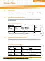
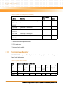
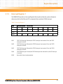
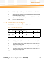
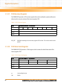
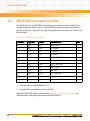
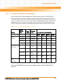
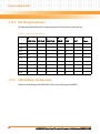
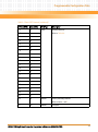
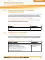
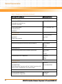
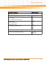
The following table describes a default memory map from the point of view of the processor
after a processor reset.
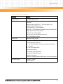
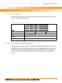
Table 2-1 Default Processor Address Map
Processor Address
Start
End
Size
Definition
Notes
0000 0000
FF6F FFFF
4087 M
Not mapped
FF70 0000
FF7F FFFF
1M
MPC8548E CCSR Registers
FF80 0000
FFFF FFFF
8M
Flash
1
1. The e500 core fetches the first instruction from FFFF FFFC following a reset.
2.1.2
Suggested Processor Memory Map
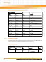
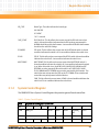
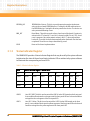
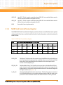
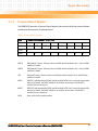
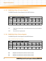
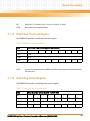
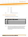
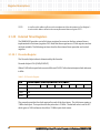
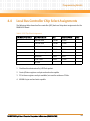
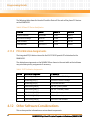
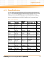
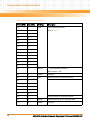
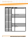
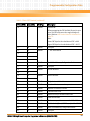
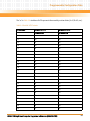
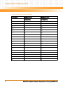
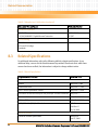
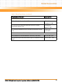
The following table describes a suggested physical memory map from the point of view of the
processor. This table reflects the address map implemented by the board level firmware at
release time.
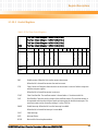
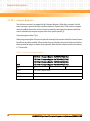
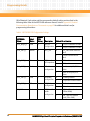
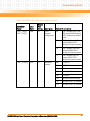
Table 2-2 Suggested Processor Address Map
Processor Address
Start
End
Size
Definition
0000 0000
top_dram - 1
dram_size
System Memory
(2 GB max)
(on-board DRAM)
8000 0000
CFFF FFFF
1.25 GB
PCI 0 Memory Space / VME
D000 0000
DFFF FFFF
256 MB
PCI 1 Memory Space
MVME4100 Single Board Computer Programmer’s Reference (6806800H19B)
21