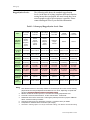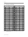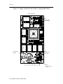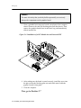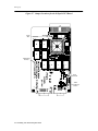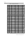
1
Eclipse3 Series
User’s Manual
Graphics Boards for PMC, PCI and CompactPCI
Compatible Computers
Rastergraf
Rastergraf, Inc.
1804-P SE First St.
Redmond, OR 97756
(541) 923-5530
FAX (541) 923-6475
web: http://www.rastergraf.com
Release 2.0
March 5, 2008
Table of Contents
INTRODUCTION...................................................................................... Introduction-1
GETTING HELP .........................................................................................................................Introduction-2
BOARD REVISIONS ...................................................................................................................Introduction-2
NOTICES ...................................................................................................................................Introduction-3
CONVENTIONS USED IN THIS MANUAL ....................................................................................Introduction-4
CHAPTER 1 GENERAL INFORMATION .............................................................. 1-1
1.1
1.2
1.3
1.3
1.4
1.5
1.6
1.7
INTRODUCTION ................................................................................................................................... 1-1
FUNCTIONAL DESCRIPTION ................................................................................................................. 1-2
ADDITIONAL REFERENCES .................................................................................................................. 1-6
ADDITIONAL REFERENCES .................................................................................................................. 1-7
SPECIFICATIONS FOR THE ECLIPSE3 .................................................................................................... 1-8
ECLIPSE3 CONNECTORS AND CABLES ............................................................................................... 1-14
MONITOR REQUIREMENTS ................................................................................................................ 1-23
CONFIGURATION INFORMATION ....................................................................................................... 1-24
CHAPTER 2 INSTALLING YOUR PERITEK GRAPHICS BOARD ................... 2-1
2.1 INTRODUCTION ................................................................................................................................... 2-1
2.2 UNPACKING YOUR BOARD ................................................................................................................. 2-2
2.3 PREPARING FOR INSTALLATION .......................................................................................................... 2-3
2.4 ECLIPSE3PMC GRAPHICS BOARD INSTALLATION .............................................................................. 2-5
2.5 ECLIPSE3PCI BOARD INSTALLATION ................................................................................................ 2-10
2.6 ECLIPSE3CPCI BOARD INSTALLATION ............................................................................................. 2-13
2.7 FINISHING THE INSTALLATION .......................................................................................................... 2-16
2.8 USING AN ECLIPSE3 BOARD IN A PC................................................................................................. 2-17
2.9 USING AN ECLIPSE3 BOARD IN A SPARC CPU ................................................................................ 2-20
2.10 USING AN ECLIPSE3 BOARD IN A POWERPC ................................................................................... 2-25
2.11 FINAL CHECKS ................................................................................................................................ 2-25
CHAPTER 3 PROGRAMMING ON-BOARD DEVICES ....................................... 3-1
3.1 INTRODUCTION ................................................................................................................................... 3-1
3.2 BOREALIS GRAPHICS ACCELERATOR .................................................................................................. 3-3
3.3 BOREALIS CLOCKS............................................................................................................................ 3-10
3.4 SYNCHRONOUS GRAPHICS RAM (SGRAM)..................................................................................... 3-11
3.5 ECLIPSE3 OPTIONAL FEATURES REGISTER ....................................................................................... 3-12
3.6 VIDEO TIMING PARAMETERS ............................................................................................................ 3-13
3.7 SYSTEM MANAGEMENT DEVICES AND FUNCTIONS........................................................................... 3-18
3.8 TALK TO ME THROUGH I2C.............................................................................................................. 3-19
3.9 DVI DIGITAL VIDEO OUTPUT ........................................................................................................... 3-20
3.10 FLASH EEPROM ............................................................................................................................ 3-22
3.11 SERIAL EEPROM ........................................................................................................................... 3-22
3.12 INTERRUPTS .................................................................................................................................... 3-22
CHAPTER 4 TROUBLESHOOTING........................................................................ 4-1
INTRODUCTION .......................................................................................................................................... 4-1
4.1 GENERAL PROCEDURES ...................................................................................................................... 4-2
4.2 DEALING WITH THE PCI BUS .............................................................................................................. 4-3
4.3 MAINTENANCE, WARRANTY, AND SERVICE ....................................................................................... 4-3
Rastergraf
Figures and Tables
Table 1-1
Table 1-2
Table 1-3
Table 1-3
Table 1-4
Table 1-5
Table 1-6
Table 1-7
Table 2-1
Table 2-2
Table 2-3
Table 3-1
Table 3-2
Table 3-3
Table 3-4
Table 3-5
Eclipse3 SDL Platform Display Timing Specifications................................. 1-9
Eclipse3 FCode/Solaris Platform Display Timing Specifications................ 1-10
Eclipse3 VGA/Windows Platform Display Timing Specifications ............. 1-10
Rastergraf Ruggedization Levels Chart........................................................ 1-13
Analog (VGA) Video Connector Pinout ...................................................... 1-16
DVI-I Connector Pinout ............................................................................... 1-17
Eclipse3 Software......................................................................................... 1-24
Common Eclipse3 Configurations ............................................................... 1-24
x86 Supported Video Modes ........................................................................ 2-19
FCode Supported Display Modes................................................................. 2-22
FCode Sync Output Modes .......................................................................... 2-23
Borealis Configuration Settings ..................................................................... 3-9
Eclipse3 ACR Register Bit Assignments ..................................................... 3-12
Standard Graphics Display Formats............................................................. 3-13
Eclipse3 Video Timing Parameter Request Form ........................................ 3-17
I2C Device Addresses ................................................................................... 3-19
Figure 1-1
Figure 1-2
Figure 2-1
Figure 2-2
Figure 2-3
Figure 2-4
Figure 2-5
Figure 2-6
Figure 2-7
Figure 2-8
Figure 3-1
Figure 3-2
Figure 3-3
Figure 3-4
Figure 3-5
Borealis Block Diagram................................................................................ 1-4
DVI Digital Video Block Digram ................................................................. 1-5
Jumper Locations for the Fab Rev 1.2 Eclipse3PMC Board ........................ 2-6
Installation of a PMC Module into an Emerson MVME2604 ...................... 2-7
Installation of a PMC Module into the PMB-C ............................................ 2-8
Installation of the PMC Module into an Emerson CPV3060........................ 2-9
Jumper Locations for the Eclipse3PCI Board............................................. 2-11
Installation of a PCI Module into an Emerson MTX.................................. 2-12
Jumper Locations for the Eclipse3CPCI Board .......................................... 2-14
Installing a CompactPCI Board .................................................................. 2-15
Borealis Block Diagram................................................................................ 3-4
Internal RAMDAC Block Diagram .............................................................. 3-7
Video Display Timing Fields ...................................................................... 3-15
THC63DV164 Block Diagram ................................................................... 3-20
THC63DV164 RGB to 24-bit TMDS Mapping Diagram........................... 3-21
Rastergraf
Introduction
This manual provides information about how to configure, install, and
program the Rastergraf Eclipse3 128-bit graphics display controllers.
Software support is available for Solaris, Linux, VxWorks, LynxOS, and
Windows 2000 and XP. They are available for PMC PCI, and
CompactPCI compatible computers.
This manual is broken down into four chapters:
Chapter 1: General Information
Chapter 2: Installing the Graphics Board
Chapter 3: Programming Devices and Memories
Chapter 4: Troubleshooting
Chapter 1 provides background material about the graphics boards.
Understanding the information in the chapter, however, is not essential for
the hardware or software installation. If you want to perform the
installation as quickly as possible, start with Chapter 2. If you have
problems installing the hardware, refer to Chapter 4 for help.
Introduction - 1
Rastergraf
Getting Help
This installation manual gives specific steps to take to install your
Rastergraf graphics board. There are, however, variables specific to your
computer configuration and monitor that this manual cannot address.
Normally, the default values given in this manual will work. If you have
trouble installing or configuring your system, first read Chapter 4,
“Troubleshooting”. If this information does not enable you to solve your
problems, do one of the following:
1)
call Rastergraf technical support at (541) 923-5530
2)
fax your questions to
(541) 923-6475
3)
send E-mail to
[email protected].
If your problem is monitor related, Rastergraf technical support will need
detailed information about your monitor.
Board Revisions
This manual applies to the following board revision levels:
Eclipse3PMC Fab Rev 1.2A
Eclipse3CPCI Fab Rev 1
Eclipse3PCI Fab Rev 0
Manual Revisions
Introduction - 2
Revision 1.0 March 19, 2001
First released version
Revision 1.1 March 25, 2001
Revisions
Revision 1.2 June 15, 2001
Minor revisions
Revision 1.3 June 25, 2001
Minor revisions
Revision 1.4 May 14, 2002
Updates for PMC 1.2
Revision 1.5 May 17, 2002
A few more changes
Revision 1.6 May 17, 2002
Release
Revision 1.7 May 17, 2002
Minor revisions
Revision 1.8 August 22, 2002
Noted Fab Rev 1.2a change for
M66EN
Revision 2.0 February 11, 2008
Created Rastergraf version. Many
detail changes
Rastergraf
Notices
Information contained in this manual is disclosed in confidence and may
not be duplicated in full or in part by any person without prior approval of
Rastergraf. Its sole purpose is to provide the user with adequately detailed
documentation to effectively install and operate the equipment supplied.
The use of this document for any other purpose is specifically prohibited.
The information in this document is subject to change without notice. The
specifications of the Eclipse3 graphics boards and other components
described in this manual are subject to change without notice. Although it
regrets them, Rastergraf assumes no responsibility for any errors or
omissions that may occur in this manual. Customers are advised to verify
all information contained in this document.
The electronic equipment described herein generates, uses, and may
radiate radio frequency energy, which can cause radio interference.
Rastergraf assumes no liability for any damages caused by such
interference.
Rastergraf products are not authorized for any use as critical components
in flight safety or life support equipment without the written consent of the
president of Rastergraf, Inc.
These products have been designed to operate in user-provided PMC,
CPCI, and PCI-compatible computers. Connection of incompatible
hardware is likely to cause serious damage. Rastergraf assumes no liability
for any damages caused by such incompatibility.
Rastergraf assumes no responsibility for the use or reliability of software
or hardware that is not supplied by Rastergraf, or which has not been
installed in accordance with this manual.
The Eclipse3 graphics boards are manufactured and sold under license
from Curtiss-Wright Controls Embedded Computing (CWCEC). Contact
Rastergraf, Inc. for additional information.
Rastergraf is a trademark of Rastergraf, Inc.
All other trademarks and copyrights are the property of their respective
owners.
Copyright © 2008 by Rastergraf, Inc.
Introduction - 3
Rastergraf
Conventions Used In This Manual
The following list summarizes the conventions used throughout this
manual.
Code
fragments
Commands or
program names
System prompts
and commands
Keyboard usage
Note
Note boxes contain information either specific to
one or more platforms, or interesting, background
information that is not essential to the installation.
Caution
Caution boxes warn you about actions that can
cause damage to your computer or its software.
Warning!
Warning! boxes warn you about actions that can
cause bodily or emotional harm.
.
Introduction - 4
Code fragments, file, directory or path names and
user/computer dialogs in the manual are presented
in the courier typeface.
Commands, or the names of executable programs,
except those in code fragments, are in bold.
Commands in code fragments are preceded by the
system prompt, a percentage sign (%), the standard
prompt in UNIX’s C shell, or the hash-mark (#),
the standard UNIX prompt for the Super-User.
<CR> stands for the key on your keyboard labeled
“RETURN” or “ENTER”
Rastergraf
Chapter 1
General Information
1.1 Introduction
The Rastergraf Eclipse3 is part of Rastergraf ’s broad line of graphics
modules for use in PMC, PCI, VME, and CompactPCI computers.
For information about all of Rastergraf ’s products, please contact
Rastergraf Worldwide Sales at (541) 923-5530 or consult Rastergraf ’s
web page at http://www.rastergraf.com.
The Eclipse3 uses a Rastergraf Borealis 2D/3D 128-bit graphics
accelerator. It features UVGA compatibility, an OpenGL pipeline, and can
address up to 32 MB of on-board SGRAM.
The Eclipse3 boards are available with either a standard VGA connector
or a DVI-I connector. When provided with the DVI-I connector, a DVI
transmitter provides 24-bit digital output encoded onto four TMDS
differential signal pairs.
The Eclipse3 boards can function as the system VGA controller and
includes an on-board flash PROM loaded with VGA BIOS for Windows
and Linux and/or OpenBoot FCode for Sun Solaris.
General Information 1-1
Rastergraf
1.2 Functional Description
As an aid to understanding the Eclipse3, a block diagram is provided at the
end of this section. The feature set includes:
• 128-bit Rastergraf Borealis 2D/3D Graphics Controller
• 33/66 MHz 32-bit PCI bus
• Embedded VGA controller
• Quad-Image BIOS supports FCode, VGA, DVI, and Sync-On-Green
• Up to 1920 x 1200 displayable analog resolution
• Up to 1280 x 1024 displayable digital (DVI) resolution
• Up to 32 MB high speed SGRAM supports multiple display pages
• Hardware pan, zoom, and scroll and bitmapped cursors
• Optional DVI Digital Output
• Non-interlaced, high refresh rate, and Sync-On-Green displays
• Optional three status LEDs (controlled by host software)
• Optional 2 Kb serial EEPROM
• Optional LM75 thermal sensor
• Optional 3.3V Regulator for systems without local 3.3V
• User selectable Sync-On-Green boot mode
• Two connector choices:
• Standard HD-15 VGA connector for RGBHV (only)
• DVI-I connector with RGBHV and DVI digital ports
• Three different PCB form factors:
• PMC single-wide module
• PCI (short)
• CompactPCI 3U board with either 3U or 6U faceplate
• Optional rear-panel I/O configuration for CompactPCI
• Ruggedized version (conformal coating and extended temperature)
• SDL Graphics Subroutine Package
• Sun/Solaris DDX 2D and 3D X Window System Servers
• Xfree86 Version 4.2 X Window System Server
• Windows 2K/XP drivers
1-2 General Information
Rastergraf
1.2.1 Borealis Graphics Controller
The Rastergraf Borealis 2D/3D graphics controller chip is a 128-bit
graphics controller with accelerated 2D and 3D patterned lines and shaded
triangles, Z buffer, and 3D volume clipping. It provides a high
performance 33/66 MHz PCI 2.1 compliant interface with no additional
external logic required.
Key Borealis Device Features
•
•
•
•
•
•
•
•
•
•
•
•
•
•
•
•
•
•
•
•
•
•
•
•
•
•
•
•
•
•
•
•
•
•
33/66 MHz PCI Interface
PCI Bus Master Event Notification
100 MHz SGRAM Memory Controller with Block Writes
Texture Mapping Capabilities
Perspective Correction
Point Sampling, Bilinear and Trilinear filtering
Full Level-of-Detail Per-Pixel MIP Mapping
Separate Texture Mipmapping Minification and Magnification filtering
Full OpenGL Texture Decal, Blend and Modulation Modes
RGB Modulation Lighting Effects
Support Palletized Textures: 1, 2, 4 and 8 bit
Support Non-Palette Textures: 8, 16, and 32 bit
Floating-point Triangle Setup with Vertex Level Commands
Flat and Gouraud Shaded line drawing, with patterning
Table and Vertex Fog
Specular Highlighting
Full Alpha blending
Alpha Compare Testing
3D Color Keying with Color Range Support
Backface Culling
Bilinearly Filtered Scaling
Power of 2 Display Zooming
Support 8, 16, 32 bits per pixels Destination Format
16 and 24 bit per pixel Z Buffer Support
Hardware 3D Volume Clipping
16-bit Logical Addressing in both X and Y
Two configurable frame buffer windows
Transparent BLT and Two operand BitBLT
Display List Processor
Color Space Converter: YUV-RGB Conversion
VGA
250 MHz RAMDAC
0.35 micron 3.3 volt CMOS process
388 PBGA (Plastic Ball Grid Array)
General Information 1-3
Rastergraf
The Borealis design is based on technology licensed by Rastergraf from
S3/Number Nine. The chip itself is manufactured for Rastergraf by LSI
Logic using LSI’s .35u G-10P ASIC process.
The Borealis graphics controller is implemented using a highly pipelined
graphic processor architecture. This architecture allows for high
performance 2D and 3D rendering. After a sequence of commands and
parameters are written, the Borealis executes the selected command
without any further host processor intervention. A Display List Processor
enables the Borealis to repetitively execute strings of commands.
The Borealis supports a local frame buffer with up to 32 MB SGRAM
using a 128-bit wide data bus. The frame buffer may be accessed as linear
buffers through the frame buffer interface or through the drawing engine.
The large local buffer may be used as a display buffer, as well as offscreen memory to be used for the storage and manipulation of bitmaps,
texture maps, Z buffering or fonts.
Figure 1-1 Borealis Block Diagram
CS[0,2]
DQM[15:0]
Linear
Windows
Controller
ADR[11:0]
WE
RAS
Display
List
Processor
AD[31:0]
Memory
SF
PA[7:0]
BE[3:0]
CNTRL[6:0]
Host Bus
Interface
PD[7:0]
2D/3D
Drawing
Engine
CJ[15:0]
MCLK
HBCLK
RST
CAS
Controller
VGA
PXD[127:0]
HSYNC
VSYNC
Internal
RAMDAC
BLANK
CRT
Controller
RED
GREEN
BLUE
CRTclk
DDC, DDA
1-4 General Information
Rastergraf
1.2.2 DVI Digital Output
The Eclipse3 may be ordered with a DVI-compliant transmitter which
provides high quality 24-bit true color digital output over twisted pair
cables up to 5 meters in length. This length may be increased by using
shielded twin-ax or fiber-optic cables. Displays ranging up to 1600 x 1200
are supported. Three TMDS data channels send data at 1.65 Gbps per
channel. Connections to the Eclipse3 are made through the front DVI-I
connector.
Figure 1-2 DVI Digital Video Block Digram
1.2.3 Software Support
Rastergraf software support is available for many operating systems.
Support for multiple display heads is included. The software packages are:
SDL Graphics Subroutine Library
Windows 2000/XP Drivers
Sun/Solaris Accelerated 2D and 3D DDX X Window System Server
Complete X Windows X11R6 server based on Xfree86 Version 4.2
Quad-Image-BIOS supports all combinations of FCode, VGA, DVI, and
Sync-On-Green.
General Information 1-5
1-6 General Information
VGA
RAMDAC
33/66 MHz
PCI 2.1
32 bit
Drawing
Engine
Display
List
Processor
Setup
Engine
PCI/PMC
Host
Bus
Interface
128
Peritek
Borealis 3D
Graphics
Accelerator
128 KB
BIOS
EEPROM
8
8
Control
Logic
LM75
Thermal
Sensor
Figure 1-3 Eclipse3 Block Diagram
CRT
Controller
SGRAM
Controller
128
16-32 MB
Display
Memory
I2C
R
G
B
H
V
Serial
EEPROM
PanelLink
Digital
Output
T
M
D
S
V
G
A
D
V
I
Rastergraf
Host PCI Bus
Rastergraf
1.3 Additional References
You can find Rastergraf documentation and technical literature on the
Rastergraf web page (http://www.rastergraf.com).
The CompactPCI Specification – PICMG R2.0 R3.0, the CompactPCI
Hot Swap Specification – PICMG 2.1 R2.0 and the CompactPCI Hot
Swap Infrastructure Interface Specification PICMG 2.12 R1.0 standards
and other information are available from PICMG:
Web Page:
https://www.picmg.org/index.stm
The PCI Local Bus 2.2 Specification is maintained by the PCI Special
Interest Group (PCISIG)
Web Page:
http://www.pcisig.com/home
Graphics Textbooks
Fundamentals of Interactive Computer Graphics
Addison Wesley, 1993.
Foley and Van Dam
Principles of Interactive Computer Graphics
McGraw-Hill, 1979
Newman and Sproull
General Information 1-7
Rastergraf
1.4 Specifications for the Eclipse3
The Eclipse3 are available in several configurations:
Analog:
Borealis graphics controller and 16 or 32 MB display
memory
DVI:
Borealis graphics controller and 16 or 32 MB display
memory and DVI-I DVI/VGA connector. Note that the
Eclipse3CPCI and Eclipse3PCI have both VGA and DVI-I
connectors.
Special Order:
LEDs, LM75 thermal sensor, Serial EEPROM, Conformal
Coating, Extended Temperature. Rear Panel I/O (CPCI J2).
Standard Features for Eclipse3 Boards
Graphics Processor:
Rastergraf Borealis 2D/3D High Performance 128-Bit
Graphics Processor has vector and pixblt functions and
programmable video timing. It supports SGRAM color and
write-per-bit register functions and includes a VGA core.
The maximum supported frequencies are 250 MHz for the
pixel clock and 100 MHz for the memory clock.
Display Memory:
Display memory is 16 MB or 32 MB of 128-bits/word, byte
addressable, no-wait state SGRAM.
16 MB of SGRAM gives eight pages of 1600 x 1200 using
8-bit pixels, four pages using 16-bit pixels, or two pages
using 32 bpp. 24 bpp packed pixel mode is not supported.
EEPROM Memory:
128 KB Flash EEPROM contains the Rastergraf Quad
Image BIOS (QIB) that supports SPARC FCode, VGA
BIOS, DVI, and Sync-On-Green (SOG). A user jumper
enables the QIB to select SOG.
Graphics Display:
The Borealis chip has an internal 250 MHz RAMDAC. It
has a 256 entry Look Up Table (LUT), which is converts 8bit pixels into full 24-bit RGB pixels. The RAMDAC has a
programmable four color bit-mapped 64 x 64 cursor. It
supports VGA and common non-interlaced displays
ranging from 640 x 480 up to 1920 x 1200. Signature
registers enable display analysis for end to end testing.
The pixel size can be 8, 15, 16, or 32-bits. For 15 and 16
bpp, the pixel is divided into Red, Green, and Blue: 5:5:5 or
5:6:5. For 32 bpp, pixel is divided into Red, Green, and
Blue (bits 24-31 are unused): 8:8:8:8.
1-8 General Information
Rastergraf
Scroll, Pan, and Zoom:
Scroll - single line (smooth scroll).
Pan - anywhere on 16 byte boundaries
Zoom: horizontal: 2, 4, 8, 16, vertical: 2, 3 ,...,15, 16
Digital Output (Optional):
The Eclipse3 can supply a digital output using a THine
THC63DV164 DVI encoder. The Borealis Video Out Bus,
which supplies TTL level RGB and Sync, is sampled and
multiplexed and driven onto 4 differential pairs.
Because of the high frequency nature of the TMDS signals,
it is vital that matched length, shielded pair cable be used
for DVI connections.
The standard front panel analog VGA connector is replaced
by a DVI-I connector. This connector supplies both the
digital DVI (TMDS) signals and VGA. Rastergraf can
supply an adapter that allows a standard VGA cable to be
used when a DVI display is not desired or available.
Composite Video Signal:
A jumper can be installed to select Sync-On-Green
operation on boot-up. The signal has the following
approximate values:
1 Volt peak to peak consisting of:
660 mV Reference White +
54 mV Reference Black +
286 mV Sync Level
Display Timing:
The Borealis chip display timing is programmable. The
following tables provide the timing values provided by
Rastergraf software.
Table 1-1 Eclipse3 SDL Platform Display Timing Specifications
Active
Display
Analog/
DVI
Format
Bits per
Pixel
Vertical
Refresh
Horizontal
Refresh
Pixel
Clock
640 x 480
Both
VGA
8, 16, 32
60 Hz
31.55 KHz
27 MHz
800 x 600
Both
SVGA
8, 16, 32
60 Hz
39.35 KHz
42 MHz
1024 x 768
Both
UVGA
8, 16, 32
70 Hz
58.86 KHz
80.52 MHz
1152 x 900
Both
Sun
8, 16, 32
66 Hz
64.92 KHz
99.72 MHz
1280 x 1024
Both
SXGA
8, 16, 32
74 Hz
82.86 KHz
141.5 MHz
1600 x 1200
Both
UXGA
8, 16, 32
60 Hz
75 KHz
162.0 MHz
1920 x 1200
Analog
WUXGA
8, 16, 32
60 Hz
75 KHz
194.4 MHz
General Information 1-9
Rastergraf
Table 1-2 Eclipse3 FCode/Solaris Platform Display Timing Specifications
Active
Display
Analog/
DVI
Bits per
Pixel
Vertical
Refresh
Horizontal
Refresh
Pixel
Clock
640 x 480
Both
8
9
8, 16, 32
60 Hz
75 Hz
31.5 KHz
37.5 KHz
25.2 MHz
31.5 MHz
800 x 600
Both
6
7
8, 16, 32
60 Hz
75 Hz
37.9 KHz
46.9 KHz
40 MHz
49.5 MHz
1024 x 768
Both
0
1
8, 16, 32
60 Hz
75 Hz
48.4 KHz
60.0 KHz
65.0 MHz
78.8 MHz
1152 x 864
Both
2
3
8, 16, 32
60 Hz
75 Hz
56.7 KHz
67.5 KHz
87.1 MHz
108 MHz
1152 x 900
Both
a
b
8, 16, 32
60 Hz
75 Hz
59.0 KHz
73.8 KHz
90.7 MHz
114.5 MHz
1280 x 1024
Both
Analog
4
5
8, 16, 32
60 Hz
75 Hz
64.0 KHz
80.0 KHz
108 MHz
135 MHz
1600 x 1200
Both
c
8, 16, 32
60 Hz
75 KHz
162.0 MHz
1920 x 1200
Analog
d
8, 16, 32
60 Hz
75 KHz
194.4 MHz
Index
Table 1-3 Eclipse3 VGA/Windows Platform Display Timing Specifications
Active
Display
640 x 480
800 x 600
Analog/
DVI
VESA
Format
Both
n/a
VGA
VGA
VGA
Both
SVGA
Bits per
Pixel
Vertical
Refresh
Horizontal
Refresh
Pixel
Clock
8, 16, 32
60 Hz
72 Hz
75 Hz
85 Hz
31.5 KHz
37.9 KHz
37.5 KHz
43.4 KHz
25.175 MHz
31.5 MHz
31.5 MHz
36 MHz
8, 16, 32
60 Hz
72 Hz
75 Hz
85 Hz
37.9 KHz
48.1 KHz
46.9 KHz
53.7 KHz
40 MHz
50 MHz
49.5 MHz
56.25 MHz
48.4 KHz
56.5 KHz
60.0 KHz
68.7 KHz
65 MHz
75 MHz
78.75 MHz
94.5 MHz
1024 x 768
Both
UVGA
8, 16, 32
60 Hz
70 Hz
75 Hz
85 Hz
1152 x 864
Both
Sun
8, 16, 32
75 Hz
67.5 KHz
108 MHz
1280 x 1024
Both
Analog
Analog
SXGA
8, 16, 32
60 Hz
75 Hz
85 Hz
64 KHz
80 KHz
91.1 KHz
108 MHz
135 MHz
157.5 MHz
1600 x 1200
Both
Analog
Analog
Analog
UXGA
8, 16, 32
60 Hz
70 Hz
75 Hz
85 Hz
75 KHz
87.5 KHz
93.8 KHz
106.3 KHz
162 MHz
189 MHz
202.5 MHz
229.5 MHz
1920 x 1200
Analog
GTF
(WUXGA)
8, 16, 32
60 Hz
75 KHz
194.4 MHz
1-10 General Information
Rastergraf
Fuse Element:
The +5V supplied to the front panel connectors is protected
by a Positive Temperature Coefficient (PTC) resistor. It
resets automatically when the overload is removed.
Local I2C Channel:
The Eclipse3 uses I2C, a 2 wire serial bus, to control the
following on-board devices:
THC63DV164 DVI transmitter (optional)
LM75 thermal sensor (optional)
AT24C02 2 Kb serial EEPROM (optional)
DDC2B display monitor control
Power-management:
With the proper software, the Borealis can power-down
unused functions and the VESA standard DDC2B lines
control the monitor.
PCI Bus Access:
Programmable Bus Address Registers (BARs) in the
Borealis map control and drawing engine registers, and
display memory through its 33/66 MHz PCI interface.
PCI bus Interrupts:
The Borealis can interrupt the PCI bus on the INTA line.
Bus Loading:
One PCI 2.1 compatible load
Module Size:
PMC:
IEEE 1386-2001,
149 mm x 74 mm, 32-bit, 33/66 MHz, J1/J2
CompactPCI: PICMG 2.0 Rev 3, IEEE 1101.10,
3U form factor w/ ESD strip,
32-bit, 33/66 MHz, J1 only, no hotswap.
3U and 6U front panel options.
Optional rear-panel module connecting to
CPCI J2 is standard 3U rear I/O format.
3U and 6U rear panel options.
PCI:
short PCI, 32-bit, 33/66 MHz, 64-bit
connector set is used for improved power
and ground distribution
PCI Subsystem Vendor ID: 0x10F0 (CW Vendor Code)
PCI Subsystem Device ID:
0x0003 for 16 MB boards, 0x0007 for 32 MB boards
Power Requirements:
Standard versions REQUIRE that the PMC, CompactPCI,
or PCI bus connectors supply both +5V and +3.3V. A
location for a local 3.3V regulator is provided on the PMC
and PCI boards for systems which do not supply 3.3V to
the backplane.
+5V +/- 5%, 0.2 A max
+3.3V +/- 5%, 1.2 A max
PCI Bus pin PRSNT1# is set low, indicating 7.5W max.
General Information 1-11
Rastergraf
Environment:
Temperature:
Humidity:
Enhanced Status:
0 to 70 degrees C, operating
-55 to +85 degrees C, storage
5% to 90%, non-condensing
Special order features include:
Three LEDs that can be driven by host CPU software.
A 2Kb Serial EEPROM stores the serial number, display
timing information, and customer specific parameters.
An LM75 thermal sensor provides limit flags and real-time
temperature read-back.
Ruggedization Option:
Rastergraf offers semi-ruggedized versions of the Eclipse3
boards include a MIL-compliant silicone or acrylic
conformal coating and extended temperature testing.
Rastergraf board designs use standard distribution
commercial temperature range parts. No formal component
tracking is maintained. .
Boards are protected with either Acrylic (MillerStephenson MS-475) or Silicone (Miller-Stephenson MS460) or equivalent and are MIL-I-46058C, Type SR and
MIL-T-152B compliant. The board is tested under extended
temperature conditions as shown on the next page.
1-12 General Information
Rastergraf
Ruggedization Levels:
The following table shows the standard ruggedization
levels. At the time of writing, complete shock and vibration
testing has not been performed, but some boards have been
tested enough to expect full acceptance is possible. Please
contact Rastergraf Sales if you need this information.
Table 1-3 Rastergraf Ruggedization Levels Chart
Spec
Air-Cooled
Level 0
Air-Cooled
Level 50
Air-Cooled
Level 100
Air-Cooled
Level 200
Conductioncooled
Level 100
Conductioncooled
Level 200
Applicable
Graphics
Board(s)
Argus
Gemini
Sirena
Eclipse3
Topaz
Garnet
Gemini
Sirena
Eclipse3
Topaz
Garnet
Gemini
Sirena
Eclipse3
Topaz
Garnet
Eclipse3
Topaz
Garnet
Garnet
Garnet
-20°C to 65°C
-40°C to 71°C
-40°C to 85°C
-40°C to 71°C
-40°C to 85°C
Operating
Temperature 0°C to 50°C
(4, 6)
Storage
-40°C to 85°C -40°C to 85°C -55°C to 125°C -55°C to 125°C -55°C to 125°C -55°C to 125°C
Humidity 0 to 95% non- 0 to 100% non- 0 to 100% non- 0 to 100% non- 0 to 100% non- 0 to 100% nonOperating condensing
condensing
condensing
condensing
condensing
condensing
Humidity
Storage
0 to 95%
condensing
0 to 100%
condensing
0 to 100%
condensing
0 to 100%
condensing
0 to 100%
condensing
0 to 100%
condensing
Vibration
Sine (1)
2 g peak
15-2 kHz
2 g peak
15-2 kHz
10 g peak
15-2 kHz
10 g peak
15-2 kHz
10 g peak
15-2 kHz
10 g peak
15-2 kHz
Vibration
Random (2)
0.01 g2/Hz
15-2 kHz
0.02 g2/Hz
15-2 kHz
0.04 g2/Hz
15-2 kHz
0.04 g2/Hz
15-2 kHz
0.1 g2/Hz
15-2 kHz
0.1 g2/Hz
15 Hz-2 kHz
Shock (3)
20 g peak
20 g peak
30 g peak
30 g peak
40 g peak
40 g peak
Conformal
Coat (5)
optional
optional
optional
optional
yes
yes
Order
Option (7)
/CA or /CS
/A5A or /A5S
/A1A or /A1S
/A2A or /A2S
/C1A or /C1S
/C2A or /C2S
Notes:
1. Sine vibration based on a sine sweep duration of 10 minutes per axis in each of three mutually
perpendicular axes. May be displacement limited from 15 to 44 Hz, depending on specific test
equipment. Shock and Vibration values not completely verified.
2. Random vibration 60 minutes per axis, in each of three mutually perpendicular axes.
3. Three hits in each axis, both directions, 1/2 sine and saw tooth. Total 36 hits.
4. Standard air-flow is 8 cfm at sea level. Some higher-powered products may require additional
airflow. Consult the factory for details.
5. Conformal coating type to be specified by customer. Consult the factory for details.
6. Temperature is measured at the card interior (not at edge).
7. Last letter in ordering option: A for Acrylic Conformal Coating, S for Silicone Conformal Coating
General Information 1-13
Rastergraf
1.5 Eclipse3 Connectors and Cables
There are two possible connector locations on the front panel of the
Eclipse3 graphics boards.
Note:
Due to front panel space limitations, the PMC board can have either the
VGA or the DVI connector installed. The PCI and CompactPCI boards
have both installed.
The Eclipse3 “Standard” versions use a standard 15-pin VGA compatible
connector. RGBHV (Red, Green, Blue, and Horizontal and Vertical sync)
and DDC/DDA monitor control signals are supplied.
The Eclipse3 DVI option use a DVI-I 29-pin connector. This connector
supplies: RGBHV (Red, Green, Blue, and Horizontal and Vertical sync),
DDC/DDA monitor control signals, as well as DVI digital video output.
An adapter connector (Molex 88741-8700, available from Digikey) is
available from Rastergraf that adapts the DVI-I to a standard VGA
connector.
The CPCI rear-panel I/O option includes a rear I/O module with VGA
and/or DVI connectors mounted to either a 3U or 6U panel.
The following sections detail the applicable pinout information.
Connector
Description
Section
15-pin D-Sub
VGA
1.5.1
29-pin DVI-I
DVI-I Connector
1.5.2
2 x 64 PMC
PMC Connections (J1 and J2)
1.5.3
1 x 96 PCI
PCI Connections (32/64)
1.5.4
1 x 125 2 mm
CompactPCI Connection (J1)
1.5.5
1 x 110 2 mm
Optional CompactPCI Connection (J2)
1.5.6
1-14 General Information
Rastergraf
1.5.1 VGA Connector
The graphics board analog output is provided on a standard VGA style
compressed 15 pin D-Sub. Alternatively, when the DVI-I connector is
used (see Section 1.5.2), an adapter (Molex 88741-8700) can be used to
supply analog video to a standard VGA computer side connector.
In either case, an “Autoscan” type monitor is used. You must use the
correct initialization, since a VGA monitor depends on the sync polarities
to determine operating frequency. The polarity of the Vertical/Composite
Sync and Horizontal Sync are controlled by the Borealis graphics
controller chip (see Section 4.5). See the Note in Section 2.9.2
concerning composite sync on green and RGBHV video out modes. If
you have problems, please contact Rastergraf for assistance.
The R, G, and B video outputs are driven by the Borealis graphics
controller chip which is capable of driving terminated cable (75 ohms) to
standard RS-330/IRE levels. Cable length should be limited to 50 feet
unless you use low loss RG-59.
Rastergraf has used an outside cable shop to build production cables:
Lynn Products, Inc.
http://www.lynnprod.com
If you really want to roll you own, the PMC board side connector is an
AMP 177802-3. The CompactPCI and PCI board side connector is an
Adam-Tech HDL15-SLB. Be sure to use 75 ohm coax for the R, G, B.
You can use TP or coax on H, and V. A cable that would work is Mogami
W3206-8 (http://www.mars-cam.com/ccd/mogami/digital3.html).
The following table provides the cable connection information:
General Information 1-15
Rastergraf
Table 1-4 Analog (VGA) Video Connector Pinout
VGA
Pin
Description
Ground Type
1
Red
75 ohm Coax with pin 6
2
Green
75 ohm Coax with pin 7
3
Blue
75 ohm Coax with pin 8
4
not used
5
DDC Ground
Circuit Ground
6
Red Ground
Circuit Ground
7
Green Ground
Circuit Ground
8
Blue Ground
Circuit Ground
9
Fused +5 Volts,
.25A max
10
Sync Ground
Circuit Ground
11
Ground
Circuit Ground
12
DDCDA
Twisted Pair with GND to pin 10
13
HSYNC
Twisted Pair with GND to pin 5
14
VSYNC
Twisted Pair with GND to pin 10
15
DDCCK
Twisted Pair with GND to pin 5
-
Connector Shell
Chassis Ground
-
Outer Shield
(Cable Jacket)
Chassis Ground
Cable Type
Warning:
The Chassis Ground MUST NOT BE CONNECTED to Circuit Ground.
1-16 General Information
Rastergraf
1.5.2 DVI-I Connector
The DVI front panel connector is a DVI-I (analog/digital)
(http://www.ddwg.org/) connector. DVI uses the DVI TMDS encoded
data format, which allows longer data cables and reduces emitted noise.
Each of the three differential pairs carries nine digital video (TTL) lines. A
separate pair carries the PLL clock for the TMDS system. TMDS requires
that the length of all pairs must be closely matched. The Borealis boards
use a THine THC63DV164 DVI transmitter. Data sheets and application
notes are available on the THine web page (http://www.thine.co.jp).
You can access the VGA from the DVI-I connector with an adapter
(Molex 88741-8700, available from Digikey). It supplies analog video
(only) to a standard VGA connector. There is no split-off for DVI. You
can also get cables and/or adapters that provide both analog and digital or
just analog or digital.
Rastergraf strongly urges you to obtain commercially manufactured cables
and/or adapters that are available from Rastergraf, Molex, and other
suppliers. But, if you really want to roll you own, the board side connector
part number is Molex 74320-1004 with Molex 71781-0001 (or equivalent)
jackposts with Loctite. A cable that would work is Mogami W3206-8
(http://www.mars-cam.com/ccd/mogami/digital6.html).
Table 1-5 DVI-I Connector Pinout
DVI-I Pin
1
2
3
6
7
8
9
10
11
14
15
17
18
19
22
23
24
4, 5, 12, 13, 16, 20, 21
C1
C2
C3
C4
C5
Description
DVI_TX2L
DVI_TX2H
DVI_TX2 Shield/Ground
DDCCK
DDCDA
Vertical Sync
DVI_TX1L
DVI_TX1H
DVI_TX1 Shield/Ground
Fused +5 Volts, .25A max
Ground
DVI_TX0L
DVI_TX0H
DVI_TX0 Shield/Ground
DVI_TXC Shield/Ground
DVI_TXCH
DVI_TXCL
n/c
Red
Green
Blue
Horizontal Sync
Analog Ground
General Information 1-17
Rastergraf
1.5.3 Connections to the PMC Bus
J11
1
3
5
7
9
11
13
15
17
19
21
23
25
27
29
31
33
35
37
39
41
43
45
47
49
51
53
55
57
59
61
63
n/c
GND
n/c
BUSMODE1L
n/c
GND
PCICLK
GND
PMCREQL
byp (Vio)
AD28H
AD25H
GND
AD22H
AD19H
byp (Vio)
FRAMEL
GND
DEVSELL
GND
n/c
PAR
byp (Vio)
AD12H
AD09H
GND
AD06H
AD04H
byp (Vio)
AD02H
AD00H
GND
J12
n/c
PINTAL
n/c
VCC (5V)
n/c
n/c
GND
PMCGNTL
VCC (5V)
AD31H
AD27H
GND
C/BE3L
AD21H
VCC (5V)
AD17H
GND
IRDYL
VCC (5V)
n/c
n/c
GND
AD15H
AD11H
VCC (5V)
C/BE0L
AD05
GND
AD03H
AD01H
VCC (5V)
n/c
2
4
6
8
10
12
14
16
18
20
22
24
26
28
30
32
34
36
38
40
42
44
46
48
50
52
54
56
58
60
62
64
1
3
5
7
9
11
13
15
17
19
21
23
25
27
29
31
33
35
37
39
41
43
45
47
49
51
53
55
57
59
61
63
n/c
n/c
n/c
GND
n/c
BUSMODE2L
PCIRSTL
VDD (3.3V)
n/c
AD30H
GND
AD24H
IDSEL
VDD (3.3V)
AD18H
AD16H
GND
TRDYL
GND
n/c
VDD (3.3V)
C/BE1L
AD14
M66EN
AD08H
AD07H
VDD (3.3V)
n/c
n/c
GND
n/c
GND
n/c
n/c
GND
n/c
n/c
VDD (3.3V)
BUSMODE3L
BUSMODE4L
GND
AD29H
AD26H
VDD (3.3V)
AD23H
AD20H
GND
C/BE2L
n/c
VDD (3.3V)
STOPL
GND
n/c
GND
AD13H
AD10H
VDD (3.3V)
n/c
n/c
GND
n/c
n/c
VDD (3.3V)
n/c
2
4
6
8
10
12
14
16
18
20
22
24
26
28
30
32
34
36
38
40
42
44
46
48
50
52
54
56
58
60
62
64
Notes: byp means the pin is connected to a bypass capacitor on the graphics board but
is otherwise not used.
1-18 General Information
Rastergraf
1.5.4 Connections to the PCI Bus
SIDE A
1
2
3
4
5
6
7
8
9
10
11
12
13
14
15
16
17
18
19
20
21
22
23
24
25
26
27
28
29
30
31
32
n/c
n/c
n/c
JTAGTDIOH
VCC (5V)
PINTAL
n/c
VCC (5V)
n/c
byp (Vio)
n/c
keyway
keyway
n/c
PPCIRSTL
byp (Vio)
PCIGNTL
GND
n/c
PAD30H
VDD (3.3V)
PAD28H
PAD26H
GND
PAD24H
PIDSELH
VDD (3.3V)
PAD22H
PAD20H
GND
PAD18H
PAD16H
SIDE B
n/c
n/c
GND
JTAGTDIOH
VCC (5V)
VCC (5V)
n/c
n/c
PRSNT1L
n/c
PRSNT2L
keyway
keyway
n/c
GND
PPCICLK
GND
PCIGNTL
byp (Vio)
PAD31H
PAD29H
GND
PAD27H
PAD25H
VDD (3.3V)
PCBE3L
PAD23H
GND
PAD21H
PAD19H
VDD (3.3V)
PAD17H
SIDE A
1
2
3
4
5
6
7
8
9
10
11
12
13
14
15
16
17
18
19
20
21
22
23
24
25
26
27
28
29
30
31
32
33
34
35
36
37
38
39
40
41
42
43
44
45
46
47
48
49
50
51
52
53
54
55
56
57
58
59
60
61
62
63
64
VDD (3.3V)
PFRAMEL
GND
PTRDYL
GND
PSTOPL
VDD (3.3V)
n/c
n/c
GND
PPARH
PAD15H
VDD (3.3V)
PAD13H
PAD11H
GND
PAD09H
keyway
keyway
PCBE0L
VDD (3.3V)
PAD06H
PAD04H
GND
PAD02H
PAD00H
byp (Vio)
n/c
VCC (5V)
VCC (5V)
GND
n/c
SIDE B
PCBE2L
GND
PIRDYL
VDD (3.3V)
PDEVSELL
GND
n/c
n/c
VDD (3.3V)
n/c
VDD (3.3V)
PCBE1L
PAD14H
GND
PAD12H
PAD10H
n/c
keyway
keyway
PAD08H
PAD07H
VDD (3.3V)
PAD05H
PAD03H
GND
PAD01H
byp (Vio)
n/c
VCC (5V)
VCC (5V)
n/c
GND
33
34
35
36
37
38
39
40
41
42
43
44
45
46
47
48
49
50
51
52
53
54
55
56
57
58
59
60
61
62
63
64
Note: byp means the pin is connected to a bypass capacitor on the graphics board but is
otherwise not used
General Information 1-19
Rastergraf
1.5.4 Connections to the PCI Bus (continued)
SIDE A
65
66
67
68
69
70
71
72
73
74
75
76
77
78
79
80
81
82
83
84
85
86
87
88
89
90
91
92
93
94
n/c
byp (Vio)
n/c
n/c
GND
n/c
n/c
GND
n/c
n/c
byp (Vio)
n/c
n/c
GND
n/c
n/c
GND
n/c
n/c
byp (Vio)
n/c
n/c
GND
n/c
n/c
GND
n/c
n/c
GND
n/c
SIDE B
n/c
n/c
GND
n/c
n/c
byp (Vio)
n/c
n/c
GND
n/c
n/c
GND
n/c
n/c
byp (Vio)
n/c
n/c
GND
n/c
n/c
GND
n/c
n/c
byp (Vio)
n/c
n/c
GND
n/c
n/c
GND
65
66
67
68
69
70
71
72
73
74
75
76
77
78
79
80
81
82
83
84
85
86
87
88
89
90
91
92
93
94
Note: byp means the pin is connected to a bypass capacitor on the graphics board but is
otherwise not used
1-20 General Information
Rastergraf
1.5.5 J1 Connections to the CompactPCI Bus
A
B
C
D
1
VCC (5V)
1
byp (-12V)
1
n/c
1
2
3
4
5
6
7
8
9
10
11
12
13
14
15
16
17
18
19
20
21
22
23
24
n/c
INTA#
n/c
n/c
PCIREQ#
AD[30]
AD[26]
CBE[3]#
AD[21]
AD[18]
keyway
keyway
keyway
VDD (3.3V)
DEVSEL#
VDD (3.3V)
n/c
VDD (3.3V)
AD[12]
VDD (3.3V)
AD[07]
VDD (3.3V)
AD[01]
2
3
4
5
6
7
8
9
10
11
12
13
14
15
16
17
18
19
20
21
22
23
24
VCC (5V)
n/c
GND
n/c
GND
AD[29]
GND
IDSEL
GND
AD[17]
keyway
keyway
keyway
FRAME#
GND
n/c
GND
AD[15]
GND
AD[09]
GND
AD[04]
VCC (5V)
2
3
4
5
6
7
8
9
10
11
12
13
14
15
16
17
18
19
20
21
22
23
24
n/c
n/c
byp (Vio)
PCIRSTL
VDD (3.3V)
AD[28]
byp (Vio)
AD[23]
VDD (3.3V)
AD[16]
keyway
keyway
keyway
IRDY#
byp (Vio)
n/c
VDD (3.3V)
AD[14]
byp (Vio)
AD[08]
VDD (3.3V)
AD[03]
byp (Vio)
2
3
4
5
6
7
8
9
10
11
12
13
14
15
16
17
18
19
20
21
22
23
24
25
VCC (5V)
25
n/c
25
n/c
25
E
byp (+12V)
TDIOH
VCC (5V)
n/c
GND
PCICLK
GND
AD[25]
GND
AD[20]
GND
keyway
keyway
keyway
GND
STOP#
GND
PAR
GND
AD[11]
n/c
AD[06]
VCC (5V)
AD[00]
VDD (3.3V)
1
2
3
4
5
6
7
8
9
10
11
12
13
14
15
16
17
18
19
20
21
22
23
24
25
VCC
(5V)
TDIOH
n/c
n/c
GNT#
AD[31]
AD[27]
AD[24]
AD[22]
AD[19]
CBE[2]#
keyway
keyway
keyway
TRDY#
n/c
n/c
CBE[1]#
AD[13]
AD[10]
CBE[0]#
AD[05]
AD[02]
n/c
VCC
(5V)
Note: byp means the pin is connected to a bypass capacitor on the
graphics board but is otherwise not used.
General Information 1-21
Rastergraf
1.5.5 J2 Connections to the CompactPCI Bus (optional)
1
2
3
4
5
6
7
8
9
10
11
12
13
14
15
16
17
18
19
20
21
22
Z
A
B
C
D
E
F
GND
GND
GND
GND
GND
GND
GND
GND
GND
GND
GND
GND
GND
GND
GND
GND
GND
GND
GND
GND
GND
GND
PK_GND
RIO_TX2L
RIO_TX2H
VIO
GND
VCC
GND
RIO_BVSYNC
RIO_DDCH
RIO_TX1L
RIO_TX1H
GND
PK_GND
RIO_TX0L
RIO_TX0H
GND
GND
GND
GND
GND
GND
GND
GND
GND
GND
GND
GND
GND
GND
GND
GND
GND
GND
GND
GND
GND
GND
RIO_BHSYNC
VIO
GND
GND
VIO
GND
GND
VIO
GND
GND
VIO
GND
GND
VIO
GND
RIO_BLU
GND
RIO_GRN
GND
GND
GND
GND
RIO_TXCH
RIO_TXCL
n/c
GND
GND
GND
n/c
RIO_RED
RIO_DDAH
GND
n/c
n/c
n/c
Note: byp means the pin is connected to a bypass capacitor on the
graphics board but is otherwise not used
Pins used for Rear Panel I/O are used in Slot 1. This board MUST
NOT be installed in Slot 1.
PK_GND are grounds that are added by Rastergraf.
1-22 General Information
Rastergraf
1.6 Monitor Requirements
Rastergraf graphics boards can be used with a variety of monitors. For
best performance a monitor should have the following features:
• VGA compatible 5 Wire RGB with separate TTL horizontal and
vertical sync or 3 Wire RGB with sync on green (see note below)
• Switchable Termination (for monitor loopthrough)
• Height, pincushion, width, phase, and position controls
• Autotracking horizontal and vertical synchronization
• See tables in Section 1.4 (above) for basic timing requirements
Notes
The Eclipse3 software defaults to standard Multiscan 5-wire RGBHV
(VGA compatible) settings. If you require Sync On Green, be sure to
install SYNC ON GREEN jumper.
Eclipse3 graphics boards DO NOT support interlaced operation.
General Information 1-23
Rastergraf
1.7 Configuration Information
The basic graphics board includes:
•
•
•
•
•
Rastergraf Borealis Graphics Processor with 8, 16, or 32 bit/pixel
16 MB SGRAM
hardware interrupts, pan, scroll, and zoom and cursors
analog video outputs
Quad Image BIOS supports VGA, FCode, DVI, and Sync on Green
(SOG)
An on-board 3.3V regulator can be provided on the PMC and PCI boards
for systems which do not supply 3.3V to the backplane. CPCI backplanes
always have 3.3V. Please contact Rastergraf for more information about
this and other special configurations.
Table 1-6 Eclipse3 Software
Operating
System
Rastergraf
OpenGL and/or
Version
Software
DirectX
DVI,
SOG
BIOS
Solaris 2.6 - 10
DDX
3.0
no
yes
FCode
Solaris 2.6 - 10
GLDX
1.0
OpenGL
n/a
FCode
Linux
Xfree86
4.2
OpenGL
yes
VGA
VxWorks
SDL
3.x
no
yes
VGA
LynxOS
SDL
3.x
no
yes
VGA
Linux
SDL
3.x
no
yes
VGA
Windows 2K, XP
2K, XP
5.x
OpenGL, DirectX
yes
VGA
Table 1-7 Common Eclipse3 Configurations
Bus Type
32 MB
DVI Rear I/O
Option Option Option
3U/6U
Option
Local 3.3V Semi-rugged
Option
Option
PMC, PCI
/32MB
/DVI
n/a
n/a
/V
See Table 1-3
CPCI
/32MB
/DVI
/RIO
/3U or /6U
n/a
See Table 1-3
Note: Please contact Rastergraf for complete Model number
information.
1-24 General Information
Rastergraf
Chapter 2
Installing Your Peritek
Graphics Board
2.1 Introduction
There are 2 steps involved in getting your Rastergraf Graphics board to
work in your system:
• Unpack and install the Rastergraf graphics board.
• Install the software
This chapter shows you how to install the Rastergraf graphics board in
your computer. Your Rastergraf software User’s Manual (e.g. SDL)
provides instructions on how to install the software.
Installing Your Peritek Graphics Board 2-1
Rastergraf
2.2 Unpacking Your Board
When you unpack your board, inspect the contents to see if any damage
occurred in shipping. If there has been physical damage, file a claim with
the carrier at once and contact Rastergraf for information regarding repair
or replacement. Do not attempt to use damaged equipment.
Caution
Be careful not to remove the board from its antistatic bag or container
until you are ready to install it. It is preferable to wear a grounded wrist
strap whenever handling computer boards.
Some operating systems require that you reboot your system after
installing a device driver, because only after the reboot will your system
utilize the driver and recognize the board. If yours is such an operating
system, you might like to install your Rastergraf software before installing
the board since you will have to shut down the computer to install the
board anyway. If you want to install the software before shutting down the
computer, proceed to the correct part of the relevant software manual and
return to this chapter afterwards.
2-2 Installing Your Peritek Graphics Board
Rastergraf
2.3 Preparing for Installation
The Eclipse3 includes three different board form factors: PMC, PCI, and
CompactPCI. In order to ease the procedure, there follows individual
sections that deal with each board type. There really aren’t any model
dependencies that affect the board installation.
2.3.1 Interrupt Settings
The Eclipse3 boards use the PCI/PMC/CPCI INTA interrupt request line
for the particular slot it is plugged into. In some computers, each slot may
map its local interrupt lines to a permuted set of INTA-INTD, which
means that the board will show up on a different interrupt line according
to the slot it is plugged into. The device driver will usually notice this and
compensate for it. In any case, the user has no direct control (e.g. jumpers)
over what interrupt line the graphics board will use.
2.3.2 Address Settings
Since the PCI bus and the Eclipse3 are configured by the operating system
and/or BIOS while booting up, there aren’t any address jumpers. The
address settings are programmable and are set up by the Eclipse3 software
as a result of information supplied by the OS at boot time. Refer to the
Rastergraf software User’s Manuals for more information.
The software sets up the BARs (Base Address Registers) in the Rastergraf
Borealis Graphics Processor that enable access to its control registers,
internal RAMDAC, DDC2B/ I2C control lines, and SGRAM.
The Rastergraf Eclipse3 device driver will load the BARs if the O/S or
BIOS did not. If you can determine the actual PCI base address, you might
even be able to probe the address spaces with an on-line debugger once
the driver code has run. Section 3.3 has details on how the Borealis
controls access to the on-board registers.
The ability to probe the board is dependent on the CPU memory map as
implemented by the system OS and the address ranges of the PCI bus as
determined by the CPU hardware. These things change from OS to OS,
board to board, and vendor to vendor, making it a difficult task. Most
likely, if you use Rastergraf supplied software, the board will show up and
you will get pictures.
Installing Your Peritek Graphics Board 2-3
Rastergraf
2.3.3 Changing the Jumpers
In the following subsections, please refer Figure 2-1 in Section 2.4 for
PMC, Figure 2-5 in Section 2.5 for PCI, and Figure 2-7 in Section 2.6 for
CompactPCI for to the parts layouts and jumper locations.
JP201: VGA PCI Device Jumper
JP201 selects the board to respond either as a PCI sub-class “VGA
Controller Device” (default) or as an “Other Display Controller” (jumper
installed). You may need to install this jumper on the second board when
you have two Eclipse3 boards installed in a PC compatible machine to
prevent the system BIOS from loading the Eclipse3 BIOS code twice.
JP101: Sync-On-Green Select Jumper
The Eclipse3 has the Rastergraf Quad Image BIOS (QIB) PROM, which
supports FCode, VGA, DVI, and Sync-On-Green (SOG). The firmware
can “determine” the need to run FCode or VGA and if the DVI monitor is
plugged in, it will select DVI mode without user intervention. However, a
separate jumper is needed to “tell” the firmware that SOG is required.
Normally, if SOG is requested prior to order shipment, JP101 is installed
at the factory. But, if it has been omitted, then install JP101 to enable
SOG.
JP202 (PMC): Reserved Jumper
JP202 is a factory use only jumper. Please do not attempt to use it.
JP233 (PCI): Local 3.3V Regulator Enable
If the graphics board was built with the optional local 3.3V regulator,
install JP233 to enable the regulator to supply power to the graphics board
when the PCI backplane only has 5V.
JP102 (CompactPCI) Frame Ground to Chassis Ground Jumpers
Ordinarily, frame ground and chassis ground are isolated from each other.
Install JP102 to connect them together.
Note:
Make sure before installing the jumper that this does not expose the
system to any electrical hazards.
2-4 Installing Your Peritek Graphics Board
Rastergraf
2.4 Eclipse3PMC Graphics Board Installation
The Eclipse3PMC board can plug into any 32-bit, 66 MHz, 5V or 3.3V
signaling IEEE 1386-2001 compatible single module PMC location. Such
locations are most commonly found on VME and CompactPCI computers.
The Eclipse3PMC can be installed in PCI and CompactPCI backplanes by
using a Rastergraf PMA-P or PMA-C passive bus adapter. Rastergraf also
supplies active carriers for PCI, the PMB-P, and a CompactPCI carrier, the
PMB-C, which can hold two PMC boards. Of course, you could also just
use an Eclipse3CPCI or Eclipse3PCI.
Note:
Older VME host or carrier boards may not supply 3.3V to the PMC
connectors and the Eclipse3 PMC boards require both 3.3V and 5V. By
special order, Rastergraf can supply the graphics board with a local 3.3V
regulator installed. Please contact Rastergraf for assistance.
Installing the PMC Graphics Board
Note:
Refer to Section 2.3.3 for the settings for JP101 and JP201.
1. Shut down the operating system and turn off the power.
Warning!
Never open the computer without turning off the power supply. Unless
internal AC wiring is exposed, leave the power cord plugged in, so as to
ground the computer chassis. You can easily get shocked, ruin computer
parts or both unless you turn off the power. Even with power switched off,
lethal voltages can exist in the equipment.
Installing Your Peritek Graphics Board 2-5
Rastergraf
Figure 2-1 Jumper Locations for the Fab Rev 1.2 Eclipse3PMC Board
JP202 - Reserved
JP201
VGA Sub-class
Device Enable
Fab Revision
Number
JP203
Optional Local
3.3V Power
JP101
Sync-On-Green
Jumper
2-6 Installing Your Peritek Graphics Board
Rastergraf
2. Open the computer and remove the CPU board onto which the
graphics PMC board is to be installed. Identify an empty PMC location
(generally there are one or two on a given CPU board). The graphics
PMC board is a Universal PMC/PCI device and can be plugged into a
PMC port which uses either 5V or 3.3V signaling.
3. Take care to optimize airflow by blocking off unused slots in the card
cage, and arrange the boards to permit optimum airflow through them.
Caution
The static electricity that your body builds up normally can seriously
damage the components on the graphics board.
Figure 2-2 Installation of a PMC Module into an Emerson MVME2604
Installing Your Peritek Graphics Board 2-7
Rastergraf
Figure 2-3 Installation of a PMC Module into the PMB-C
t1
lo
CS
PM
t0
lo
CS
PM
2-8 Installing Your Peritek Graphics Board
Rastergraf
Figure 2-4 Installation of the PMC Module into an Emerson CPV3060
4. Touch a metal part of the computer chassis, remove the graphics board
from its anti static bag, and immediately slip it into the slot. After
ensuring that the board is seated correctly, install the mounting screws
(two near the front and two near the PMC connectors).
Note
Sometimes the graphics board front panel can hang up going into the
carrier front panel hole. This can be because there is a little rubber EMI
gasket that is installed in a slot cut into the graphics board front panel. If
the hole in the carrier board is “on the small side” it can be difficult if not
impossible to install the graphics board. In this case, you will have to
remove and discard the gasket.
5. Close the computer.
Now, go to Section 2.7.
Installing Your Peritek Graphics Board 2-9
Rastergraf
2.5 Eclipse3PCI Board Installation
The Eclipse3PCI board is “Universal PCI” device and is designed to plug
into any standard PCI 2.2 specification compatible backplane. Although it
is a 32-bit device, it includes the 64-bit expansion connector to take
advantage of the extra power and ground pins (no signals are used). It can
be plugged into a slot which uses either 5V or 3.3V signaling protocol.
Note:
The Eclipse3PCI boards require both 3.3V and 5V. Most AT style
motherboards do not supply 3.3V to the PCI connectors. If the computer is
listed as PCI 2.0 or 2.1 compliant, it probably does not supply 3.3V.
By special order, Rastergraf can supply the graphics board with a local
3.3V regulator installed. Please contact Rastergraf for assistance.
Installing the PCI Graphics Board
Note:
Refer to Section 2.3.3 for the settings for JP101, JP201, and JP233.
1. Shut down the operating system and turn off the power.
Warning!
Never open the computer without turning off the power supply. Unless
internal AC wiring is exposed, leave the power cord plugged in, so as to
ground the computer chassis. You can easily get shocked, ruin computer
parts or both unless you turn off the power. Even with power switched off,
lethal voltages can exist in the equipment.
2. Open the computer and find an empty PCI slot.
When installing the card you have to watch out because the slot (see
Figure 2-5) between the 32-bit and 64-bit parts of the PCB connector
is quite narrow. PCs sometimes have PCI connectors that have overly
thick moldings, requiring the slot to be widened. Should you encounter
this problem, please contact Rastergraf for assistance.
2-10 Installing Your Peritek Graphics Board
Rastergraf
Figure 2-5 Jumper Locations for the Eclipse3PCI Board
32/64 bit
PCI slot
JP201
VGA
JP101
Flash Bank
Fab Revision
Number
JP233
Local 3.3
Installing Your Peritek Graphics Board 2-11
Rastergraf
Caution
The static electricity that your body builds up normally can seriously
damage the components on the graphics board.
3. Wear a grounded wrist strap and touch a metal part of the computer
chassis. Remove the card slot blocking plate from the chassis. Then,
remove the graphics board from its anti static bag, and immediately
slide it into the slot.
Figure 2-6 Installation of a PCI Module into an Emerson MTX
4. After making sure the board is seated correctly, install the screw into
the place where the blocking plate was and which (now) holds the
graphics board’s front panel
5. Close the computer.
Now, go to Section 2.7
2-12 Installing Your Peritek Graphics Board
Rastergraf
2.6 Eclipse3CPCI Board Installation
The Eclipse3CPCI board can plug into any 32-bit, 5V or 3.3V signaling
CompactPCI 3U or 6U slot. Although the board is usually supplied with a
6U faceplate, a 3U faceplate is also available. The board uses only the J1
connector unless the Rear I/O option is included.
Installing the Graphics Board
Note:
Refer to Section 2.3.3 for the settings for JP101, JP102, and JP201.
1. Shut down the operating system and turn off the power.
Warning!
Never open the computer without turning off the power supply. Unless
internal AC wiring is exposed, leave the power cord plugged in, so as to
ground the computer chassis. You can easily get shocked, ruin computer
parts or both unless you turn off the power. Even with power switched off,
lethal voltages can exist in the equipment.
2. Open the computer and identify the empty slot in the card cage that is
closest to the CPU. Do not leave any slots empty between the graphics
board and the CPU.
The Eclipse3CPCI board is a Universal PCI device and can be plugged
into a slot which uses either 5V or 3.3V signaling protocol. Therefore,
a J1 connector signaling key plug is not necessary.
3. In the interest of allowing air flow, and if you have a choice, block off
any unused slots in the cardcage so that fan air will not flow through
them.
Installing Your Peritek Graphics Board 2-13
Rastergraf
Figure 2-7 Jumper Locations for the Eclipse3CPCI Board
JP201
VGA
Fab Revision
Number
JP101
Flash Bank
JP102
Frame/Chassis
Ground
2-14 Installing Your Peritek Graphics Board
Rastergraf
Caution
The static electricity that your body builds up normally can seriously
damage the components on the graphics board.
4. Wear a grounded wrist strap. Touch a metal part of the computer
chassis, remove the graphics board from its anti static bag, and
immediately slide it into the slot.
Figure 2-8 Installing a CompactPCI Board
5. After making sure the board is seated correctly, lever the card in with
the injector(s) and tighten the screwlock on each end of the faceplate.
Now, go to Section 2.7.
Installing Your Peritek Graphics Board 2-15
Rastergraf
2.7 Finishing the Installation
2.7.1 Connecting to the Monitor
If you have an Eclipse3 Standard version board, plug a VGA cable into the
VGA compatible front panel connector.
If you have an DVI option board, use either a Rastergraf supplied breakout
cable or your own cable solution and plug into the DVI-I connector on the
graphics board’s front panel. You can use either a VGA (analog) or digital
(DVI) compatible monitor.
In either case, be sure to snug the connector’s thumbscrews down, as it
may otherwise work loose and cause unreliable operation. Make sure that
the 75 ohm switch on the monitor, if there is one, is turned on.
2.7.2 Checking your Display
Note
The Eclipse3 boards can supply 3 Wire (RGB with sync on green, BNC
connectors) or 5 Wire Video (RGBHV, VGA connector). Rastergraf
software defaults to 5 Wire Video (NO sync on green).
Be aware that if you connect a board that has video parameters set up for
sync on green to a VGA compatible monitor you will get a green
background on the display.
Another minor detail:
The Eclipse3 board may, depending on its original configuration as
supplied by Rastergraf, have its BIOS PROM programmed with VGA
BIOS, Sun SPARC compatible FCode, or, most commonly, both.
In the two former cases, obviously you can only use the board in a PC or
SPARC, respectively. In the latter case, you should be able to use the
board in either a PC or SPARC, and the system BIOS or OpenBoot should
figure out what to do.
Now, turn on the power and check your monitor’s display and proceed.
2-16 Installing Your Peritek Graphics Board
Rastergraf
2.8 Using an Eclipse3 Board in a PC
2.8.1 Multiboard Operation
The Windows 2000 and Windows XP drivers and Linux SDL and X Free
86 4.2 support multihead operation.
Single Graphics Board
If you are using a PC and the Rastergraf board is to be the system display
(and you don't have another VGA controller installed), the system BIOS
should find the Rastergraf board, and initialize the display.
Multiple Graphics Boards
If you do have another VGA board in the system, the order in which the
boards are plugged into the backplane or motherboard will determine
which board will be used for the system display. If the BIOS picks the
wrong one, turn off the computer and swap the boards' positions.
If your system has a non-removable VGA controller and you want to use
the Rastergraf board as the system display you may have a problem. If the
BIOS starts up using the built-in VGA, you may be able to disable it with
a BIOS setting. Otherwise, contact the system board manufacturer. Failing
these things, you are probably out of luck.
2.8.2 Rastergraf Quad Image BIOS VGA Image
The Rastergraf E3 boards feature four 32KB BIOS images, suitable for
both x86 (Windows, DOS, Linux) and FCode (Sun). The images conform
to the PCI R2.2 Expansion ROM specification. The PROM is organized as
VGA, FCode, VGA with Sync-On-Green, and FCode with Sync-OnGreen for a total size of 128KB. For maximum compatibility with noncompliant systems the x86 image precedes the FCode image.
The Sync-On-Green jumper selects the one or the other half of the PROM.
On boot up the system BIOS locates and runs the appropriate ROM code.
Note: not all E3 boards have the jumper pins installed. Check with your
sales representative if you need this feature.
Installing Your Peritek Graphics Board 2-17
Rastergraf
x86 Image Features:
Support for the 16 standard DOS modes as well as 25 extended VESA
modes. See the complete list below. Other extended VESA modes may be
added in the future. All standard DOS, VESA and VESA32 functions are
supported including DVI, refresh rate, power management and DDC.
The Sync-On-Green modes supports the standard DOS modes with
"XOR" composite sync and VESA modes with true serrated / equalized
composite sync with pedestal. This is a separate image, selectable by the
JP101 jumper.
The BIOS code will search for and initialize the DVI chip, if that option is
installed on the E3 board. The DVI output is simultaneous with the analog
output, so either monitor plugged into the E3 will work. In the case of
Sync-On-Green image and the E3 has the DVI option installed and a DVI
monitor is connected then the Sync-On-Green will be disabled, as it is not
compatible with DVI. If a DVI monitor is not detected Sync-On-Green
will not be disabled, but if a DVI monitor is later connected it may not
display properly.
During boot, the BIOS will display a message screen for 10 seconds
before relinquishing control back to the system BIOS. This screen will
identify the Borealis board BIOS, the revision and build date, and
copyright Rastergraf Corp. Additional messages will be displayed if a DVI
option is found, if a DVI monitor is connected, if it is a Sync-On- Green
image, if the Sync-On-Green is disabled due to a DVI monitor being
detected, and a warning if the motherboard is found to not be fully PCI
compliant. Other diagnostic messages may be added in the future.
A TSR image is also available. In the case of booting DOS this allows
switching to a different (e.g. more current) version after boot, or switching
to or from Sync-on-Green mode. This is recommended for testing only,
the longer term action is to reprogram the image, which can be done at the
factory, or in the field in some cases.
Note that both analog (RGB) and DVI are supported by the BIOS code.
Connection to a DVI monitor is detected and the appropriate register
values are set without the need to have the user set any special flags or
jumpers.
2-18 Installing Your Peritek Graphics Board
Rastergraf
Table 2-1 x86 Supported Video Modes
Type
DOS
DOS
DOS
DOS
DOS
DOS
DOS
DOS
DOS
DOS
DOS
DOS
DOS
Code
0x00,1
0x02,3
0x04,5
0x06
0x07
0x0D
0x0E
0x0F
0x10
0x11
0x12
0x13
0x6A
Type
VESA
VESA
VESA
VESA
VESA
VESA
VESA
VESA
VESA
VESA
VESA
VESA
VESA
VESA
VESA
VESA
VESA
VESA
VESA
VESA
VESA
VESA
VESA
VESA
VESA
Code
0x0100
0x0101
0x0103
0x0105
0x0107
0x0110
0x0111
0x0112
0x0113
0x0114
0x0115
0x0116
0x0117
0x0118
0x0119
0x011a
0x011b
0x0120
0x0121
0x0122
0x0123
0x0124
0x0125
0x0126
0x0127
Text
40x25
80x25
40x25
80x25
80x25
40x25
80x25
80x25
80x25
80x30
80x30
40x25
--
Graphics
-320x200
640x200
-320x200
640x200
640x350
640x200
640x480
640x480
320x200
800x600
Graphics
640 x 400
640 x 480
800 x 600
1024 x 768
1280 x 1024
640 x 480
640 x 480
640 x 480
800 x 600
800 x 600
800 x 600
1024 x 768
1024 x 768
1024 x 768
1280 x 1024
1280 x 1024
1280 x 1024
1600 x 1200
1600 x 1200
1600 x 1200
1600 x 1200
1152 x 864
1152 x 864
1152 x 864
1152 x 864
Color Range
4 bits per pixel
2 bits per pixel
4 bits per pixel
monochrome
monochrome
4 bits per pixel
4 bits per pixel
monochrome
4 bits per pixel
monochrome
4 bits per pixel
8 bits per pixel
4 bits per pixel
PC Mode
CGA
CGA
CGA
CGA
MDA
EGA
EGA
EGA
EGA
VGA
VGA
VGA
SVGA
Color Range
PC Type
8 bits per pixel
-8 bits per pixel
VGA
8 bits per pixel
SVGA
8 bits per pixel
UVGA
8 bits per pixel
SXGA
15 bits per pixel
VGA
16 bits per pixel
VGA
32 bits per pixel
VGA
15 bits per pixel SVGA
16 bits per pixel SVGA
32 bits per pixel SVGA
15 bits per pixel UVGA
16 bits per pixel UVGA
32 bits per pixel UVGA
15 bits per pixel SXGA
16 bits per pixel SXGA
32 bits per pixel SXGA
8 bits per pixel
UXGA
15 bits per pixel UXGA
16 bits per pixel UXGA
32 bits per pixel UXGA
8 bits per pixel
Sun
15 bits per pixel
Sun
16 bits per pixel
Sun
32 bits per pixel
Sun
Installing Your Peritek Graphics Board 2-19
Rastergraf
2.9 Using an Eclipse3 Board in a SPARC CPU
2.9.1 Multiboard Operation
The Rastergraf loadable DDX module supports multihead operation under
Solaris 8 with Xinerama.
If you are running on a Sun system, you should have the Rastergraf
OpenBoot FCode image loaded into the graphics board. This will enable
OpenBoot to correctly identify the graphics board on startup and use it as
the console.
Single Graphics Board
If the Rastergraf board is to be the system display (and you don't have
another display board installed), OpenBoot should find the Rastergraf
board, and initialize the display.
Multiple Graphics Boards
If you do have another display board in the system, the order in which the
boards are plugged into the backplane or motherboard will determine
which board will be used for the system display. If OpenBoot picks the
wrong one, swap cables or turn power off and swap the boards' positions.
If your system has a non-removable VGA controller and you want to use
the Rastergraf board as the system display you may have a problem. If
OpenBoot starts up using the built-in VGA, you may be able to disable it
with an OpenBoot EEPROM setting. Otherwise, contact the system board
manufacturer. Failing these things, you are probably out of luck.
2.9.2 Using OpenBoot and the Rastergraf FCode on Eclipse3
Eclipse3 has the capability to function as a console device using the
embedded OpenBoot FCode firmware programmed into the Eclipse3
board.
The display defaults to 1152 x 864 @ 60hz, 8 bits per pixel with separate
horizontal and vertical sync signals and black text on a white background.
Please skip to Section 2.13 if you do not wish to change the default
(startup) appearance of the display.
Note that both analog (RGB) and DVI are supported by the BIOS code.
Connection to a DVI monitor is detected and the appropriate register
values are set without the need to have the user set any special flags or
jumpers.
2-20 Installing Your Peritek Graphics Board
Rastergraf
2.9.2.1 Getting Ready to Make the Changes
If you are running Solaris, shutdown and halt the CPU until the OpenBoot
prompt (ok) appears.
Then, disable the CPU from automatically booting until the configuration
process is completed:
ok setenv auto-boot? false
Set the OpenBoot input and output devices to recognize Eclipse.
ok setenv input-device keyboard
ok setenv output-device screen
2.9.2.2 NVEDIT Command Summary
The next section makes use of the OpenBoot nvedit utility to change the
default settings for the Rastergraf FCode that are maintained in the
nvramrc file by OpenBoot.
NVEDIT Commands
Ctrl-N
Go to the next line
Ctrl-P
Go to the previous line
Ctrl-A
Go to the beginning of a line
Ctrl-L
List the entire contents
Ctrl-K
Deletes a line
Ctrl-C
Exits the editor
Hitting the <Enter> key while in nvedit causes a new empty line to be
inserted in the nvramrc.
Important Note: in order for the changes that have been made in nvram
to take effect some processor boards (e.g., the Themis UltraSparcII) may
require the following to be added as the last line of the nvramrc.
probe-all install-console banner
Installing Your Peritek Graphics Board 2-21
Rastergraf
2.9.2.3 Setting the Console Resolution
The initial system default console resolution of the Eclipse3 is 8 bits per
pixel, 1152 x 864 @ 60Hz. The Eclipse3 is capable of supporting
additional console mode resolutions (all are 8 bpp) as shown in the
following table:
Table 2-2 FCode Supported Display Modes
Index
0
1
2*
3
4
5
6
7
8
9
a
b
c
d
Graphics
Refresh Rate
1024 x 768
1024 x 768
1152 x 864
1152 x 864
1280 x 1024
1280 x 1024
800 x 600
800 x 600
60 Hz
75 Hz
60 Hz
75 Hz
60 Hz
75 Hz
60 Hz
75 Hz
60 Hz
75 Hz
60 Hz
75 Hz
60 Hz
60 Hz
640 x 480
640 x 480
1152 x 900
1152 x 900
1600 x 1200
1920 x 1200
PC Type
UVGA
UVGA
Sun
Sun
SXGA
SXGA
SVGA
SVGA
VGA
VGA
Sun (old)
Sun (old)
UXGA
WUXGA
Index * - initial system default
To change the startup console display mode, identify the desired graphics
resolution and refresh rate and enter the corresponding index value (e.g, 6
is the index value for 800 x 600 @ 60hz) in place of the word index, as
shown in the below.
[at the ok prompt]
type
nvedit
receive 0:
[if, instead, you receive 0: and some text, type <ctrl-k> to clear the line]
type
index constant eclipse3-console-mode <return>
receive 1:
[if, instead, you receive 1: and some text, just ignore it]
type
^C
receive ok
type
nvstore
receive ok
2-22 Installing Your Peritek Graphics Board
Rastergraf
2.9.2.4 Setting the Sync Mode
The initial system default sync signal output type of Eclipse3 is separate,
positive polarity. Eclipse3 is capable of generating additional sync output
signals as shown in the following table:
Table 2-3 FCode Sync Output Modes
Mode
0*
1
2
3
4
5
6
7
Sync
Mode
Horizontal
Polarity
Vertical
Polarity
negative
negative
negative
negative
negative
Blanking
Pedestal
n/a
n/a
n/a
n/a
n/a
Separate
Separate
Separate
Separate
Composite
Reserved
Sync on Green
Sync on Green
positive
positive
negative
Reserved
Reserved
Reserved
Reserved
negative
negative
negative
negative
yes
no
yes
yes
positive
positive
Install
JP101
no
no
no
no
no
I* - initial system default
If you do not wish to change the display mode, please skip to the next
section.
To change the startup sync output mode, identify the desired sync output
mode and enter the corresponding index value (e.g, 6 is the index value for
Sync On Green with Blanking Pedestal) in place of the word mode, as
shown below.
[at the ok prompt]
type
nvedit
receive 0: <index> constant eclipse3-console-mode
[if, instead, you receive 0: but no text, it means that the console mode is not set]
type
<return>
receive 1:
[if, instead, you receive 1: and some text, type <ctrl-k> to clear the line]
type
mode constant eclipse3-console-sync <return>
receive 2:
[if, instead, you receive 2: and some text, just ignore it]
type
^C
receive ok
type
nvstore
receive ok
Installing Your Peritek Graphics Board 2-23
Rastergraf
2.9.2.5 Setting the Console Background and Text Display Appearance
The initial system default console background and text display appearance
is Black Text on a White Background.. Alternatively, White Text on a
Black Background (it will look like this: Eclipse3).
To change the appearance, enter the new mode (0 for Black Text, 1 for
White Text) in place of the word appear, as shown below.
[at the ok prompt]
type
nvedit
receive 0: <index> constant eclipse3-console-mode
[if, instead, you receive 0: but no text, it means that the console mode is not set]
type
<return>
receive 1: <mode> constant eclipse3-console-sync
[if, instead, you receive 1: but no text, it means that the console sync is not set]
type
<return>
receive 2:
[if, instead, you receive 2: and some text, type <ctrl-k> to clear the line]
type
appear constant eclipse3-console-background <return>
receive 3:
[if, instead, you receive 3: and some text, just ignore it]
type
^C
receive ok
type
nvstore
receive ok
2.9.2.6 Activating Eclipse3 Console Mode Features
To display the nvramrc contents:
[at the ok prompt]
type
printenv nvramrc
receive 0: <index> constant eclipse3-console-mode
receive 1: <mode> constant eclipse3-console-sync
receive 1: <appear> constant eclipse3-console-background
<index>, <mode> and <appear> will be the values you entered. Now,
make OpenBoot to use the information contained within nvram:
type
receive
type
receive
type
^C
ok
setenv use-nvramrc? true
ok
reset
2-24 Installing Your Peritek Graphics Board
Rastergraf
2.10 Using an Eclipse3 Board in a PowerPC
If the CPU's on-board firmware is VGA aware, it should initialize the
graphics board and use it as the system console. However, many PowerPC
(PPC) based computers don't have generic VGA support. Newer ones are
not "chrp" or "prep" compliant anymore, so they don't know about FCode.
Your best bet is to use a board with a VGA BIOS in it.
Otherwise, you will have to boot using a serial terminal and only after the
graphics software has been installed and run will you see anything.
2.11 Final Checks
If you are running in a PC, then you should get the usual PC displays. If
you have multiple graphics boards installed, only one will be initialized by
the BIOS. Once you have installed the Windows NT/2K/XP multihead
drivers and reboot, all screens will be initialized as the OS boots.
In the case of X Windows, your monitor should display a uniform stippled
raster and a cross-hair cursor, which is controlled by the mouse. If you
have multiple graphics boards installed, all screens will be initialized and
display the stipple once you have the server installed and running.
For SDL, demo programs are provided that may be run to put test patterns
on the screen(s).
Pictures!
Once you have a picture on the screen, you may need to adjust the width,
height, brightness, contrast, and hold controls on your monitor to get a
good, centered image. If these controls don’t adjust the image properly,
the parameters used to set the graphics timing registers might be wrong. If
you have any trouble with any part of the installation call or email
Rastergraf for assistance, or refer to Chapter 4.
Installing Your Peritek Graphics Board 2-25
Rastergraf
Chapter 3
Programming On-board
Devices
3.1 Introduction
This chapter covers the special programming features of the individual
devices used on the Eclipse3. It is intended to supply information unique
to the board or to the application of a particular chip. Section 1.3 provides
a list of appropriate publications that include manufacturer’s data sheets
and manuals.
Rastergraf offers a variety of software to support the Eclipse3 graphics
boards in Solaris, Windows 2000, and XP, VxWorks, and Linux. These
offerings are covered in detail on the Rastergraf web page.
Programming On-board Devices 3-1
Rastergraf
Note
Please read these sections before starting on this chapter:
Section 1.2
Chapter 2
Functional description of the Eclipse3 boards.
Installation
This chapter includes the following other sections:
3.2
3.3
3.4
3.5
3.6
3.7
3.8
3.9
3.10
3.11
3.12
Borealis Graphics Accelerator
Synchronous Graphics RAM (SGRAM)
Borealis Clocks
Video Timing Parameters
Eclipse3 Auxiliary Registers
System Management Devices
Talk to Me Through I2C
DVI Digital Video Output
Flash EEPROM
Serial EEPROM
Interrupts
Because the Eclipse3 is mostly an assembly of “black box” parts, there
isn’t a lot of external logic that has to be documented. Thus, the following
sections don’t actually provide much programming information, as the
chip documentation and SDL device support cover that pretty well. The
sections summarize the devices and include some “hints and kinks”.
You can refer to the Rastergraf web site for complete documentation.
You can also license the Rastergraf SDL source code itself.
The following sections assume that you have read Section I.2 and have
some knowledge of video, graphics, the PCI bus and the I2C protocol. For
detailed information concerning operation of the PCI bus, please refer to
the Section 1.3, Additional References.
3-2 Programming On-board Devices
Rastergraf
3.2 Borealis Graphics Accelerator
Note
The Borealis Technical Manual is available from Rastergraf under NDA.
3.2.1 Introduction
This section describes the architecture and includes a block diagram for
Borealis high performance graphics controller, which includes a 33/66
MHz PCI compliant interface with no additional external logic required.
Please see the following page for a Block Diagram of the Borealis.
Software may interact with Borealis by directly manipulating pixels
through the frame buffer interface or by the Borealis3D’s highly pipelined
graphic processor architecture. This architecture allows for high
performance 2D and 3D Rendering. After a sequence of commands and
parameters are written, Borealis executes the selected command without
any further host processor intervention.
3.2.2 Host Bus Interface
The Host Bus Interface provides an interface to the PCI system bus. It
implements a full PCI slave interface, responding to reads and writes of
configuration, memory, and I/O cycles. It also implements a PCI master
interface for specific memory writes. It also generates peripheral bus
control for flash EPROM.
3.2.3 Frame Buffer
Borealis supports one local frame buffer of up to 32 MB with a data bus
width of 128 bits to SGRAM memory. The local buffer may be used as a
display buffer, as well as off-screen memory to be used for the storage and
manipulation of bitmaps, texture maps, Z buffering or fonts. The buffer
may be accessed as a linear buffer through the Frame Buffer interface or
through the drawing engine.
.
Programming On-board Devices 3-3
Rastergraf
Block Diagram
Borealis is partitioned into the following functional sections:
•
•
•
•
•
•
•
Host Bus Interface
Aperture Controller
Drawing Engine
CRT Controller
Memory Controller
Internal VGA
Internal RAMDAC
CS[0,2]
DQM[15:0]
Linear
Windows
ADR[11:0]
Controller
WE
RAS
Display
List
AD[31:0]
Memory
SF
Processor
BE[3:0]
CNTRL[6:0]
CAS
Controller
PA[7:0]
Host Bus
Interface
PD[7:0]
2D/3D
Drawing
CJ[15:0]
Engine
MCLK
HBCLK
RST
VGA
PXD[127:0]
HSYNC
VSYNC
Internal
RAMDAC
BLANK
CRT
Controller
RED
GREEN
BLUE
CRTclk
DDC, DDA
Figure 3-1 Borealis Block Diagram
3-4 Programming On-board Devices
Rastergraf
3.2.4 Linear Windows Controller
The Linear Windows Controller provides address decoding, address
translation, color space conversion between the host interface and the local
memory system. It also provides a mechanism for caching reads and
writes from the host bus to the local buffers. In write mode, up to eight 32
bit words may be written to the host bus cache. The cache continuously
monitors the address of each word written to determine if they are in the
same page. If the words are not in the same page, or if the cache word
count reaches eight, the cache will request the required number of memory
writes from the Memory Controller. At this time the cache controller
swaps access to its second cache and continues to accept host writes. If
another page fault is detected during the secondary cache fill, a system
stall will occur. This situation can be avoided by testing the cache and by
doing cache line fills. During reads latency will be incurred for initial
accesses or any page fault conditions. Software should make an effort to
maintain scan line coherency during any access to the local buffers for
optimal performance.
3.2.5 Drawing Engine
The Drawing Engine provides all the required logic to implement
BITBLT, LINE, LINE_3D, TRIAN_3D, and HOST XFER commands.
The Drawing Engine, when triggered, transfers command and parameter
information from the host accessible registers to its own local working
registers where it begins its setup phase. When the Drawing Engine is
done with its setup, it begins the execution of a specific algorithm for the
associated command.
For non-rendering commands, after the setup phase, the Drawing Engine
begins requesting memory access from the Memory Controller. For 2D
and/or 3D rendering commands, the object is piped through the
algorithmic rendering engine which begins requesting memory access
from the Memory Controller as soon as the first pixel/texel is generated.
Up to 2 rendering commands can be piped through the rendering engine at
the same time.
If read data is requested, the memory controller will control the loading of
the data into the Drawing Data path and will notify the Drawing Engine
that the data is now available. If write data is requested, the data will have
been previously setup in the drawing data path and the Memory Controller
will control the output of that data to the selected memory buffer.
Programming On-board Devices 3-5
Rastergraf
3.2.6 Display List Processor
The Display List Processor (DLP) is used to feed a set of commands to the
Drawing Engine. The DLP uses a 128-bit instruction word. The instruction
formats allow for each word to write up to three Drawing Engine registers
or two text glyphs. There is a four register mode which only writes XY0,
XY1, XY2, and XY3. This mode cannot be mixed with any other mode.
3.2.7 CRT Controller
The CRT Controller provides programmable CRT timing signals:
horizontal, vertical blanks and syncs. It is also responsible for generating
requests to the memory controller for screen refresh cycles. A free running
frame counter which generates interrupts to the Host is also provided. This
is useful for synchronizing bit map copies. CRT Controller also provides
display refresh data for the internal RAMDAC.
3.2.8 Memory Controller
The Memory Controller arbitrates and controls all access to the local
memory buffer by the Host Interface, the CRT controller, and the Drawing
Engine. This unit provides support for SGRAM memory.
3.2.9 VGA Core
The Borealis incorporates an IBM-compatible VGA core. The VGA core
implements the standard VGA register set for the various VGA
components (CRT controller, sequencer, graphics controller, attribute
controller, etc.) and is capable generating the standard VGA modes (00h 07h, 00h - 13h). The control of memory and CRT signals can be switched
between the VGA core and the Borealis. The VGA memory space is
shared with the Borealis frame buffer and is sparsely mapped within it.
3-6 Programming On-board Devices
Rastergraf
3.2.10 Internal RAMDAC and PLL Clock Generators
The RAMDAC transforms the raw data from the CRT controller into
signals that an analog or digital monitor can understand. In the process, it
can add gamma correction and a high resolution cursor. The RAMDAC
also provides two programmable clocks which can range from 25 MHz to
250 MHz: one for the memory controller, and the other for the pixel data.
Feature Summary
•
•
•
•
•
•
•
•
•
•
•
•
•
•
250 MHz operation
128-bit > 64-bit multiplexer from the pixel FIFO
Fine-grained PLL programming optimizes display
Pixel re-synchronization ensures integrity of all display modes
Large Screen ISO-compliant refresh rates
8/15/16/32-bits per pixel
32 bpp Direct Color Gamma correction
256-shade gray scale
Three 256x8 color palette RAMs
Triple monotonic 8-bit DACs
64x64/32x32 translucent hardware cursor
100 MHz 8-bit VGA data input
On-chip diagnostic functions
Power-down modes
Figure 3-2 Internal RAMDAC Block Diagram
Programming On-board Devices 3-7
Rastergraf
3.2.11 Coordinate System
The screen coordinate system has its origin at the upper left hand corner of
the screen, with the X coordinates incrementing left to right and the Y
coordinates incrementing top to bottom. The coordinate system for a 1280
by 1024 display is shown in below.
(0,0)
(0,1023)
(1279,0)
(1279,1023)
Everything performed in X-Y space is done using 16-bit 2's complement
integers. This includes: destination X and Y coordinates, registers that are
specified in XY format, and arithmetic operations.
Rendering commands use X and Y coordinates that are specified in IEEE
Single Precision Floating Point (ISPFP) format and then converted to 16bit 2's complement integers.
In all cases, no overflows will be detected or reported. Care must be
taken for drawing operations not to exceed the 16 bit coordinate space.
The display buffer is accessed in this format by specifying the coordinate,
the source and/or destination space origin, and the buffer pitch. From this
organization it can be seen that the pitch of the display buffer can be
changed on a command by command basis.
The Z buffer can be either 16 bits in 16 bpp mode or 24 bits (packed into
the lower 3 bytes of a 4 byte DWORD) in 32 bpp mode. As with the
display buffer, the Z buffer can be accessed by specifying the Z buffer
origin, Z buffer pitch and the (x,y) coordinate of the Z buffer. The Z
values goes through an ISPFP setup engine and are converted to the
appropriate format (16 or 24 bits) before it is stored into the Z buffer.
3-8 Programming On-board Devices
Rastergraf
3.2.12 Borealis Build Options and Power-up Settings
The Borealis is a “Plug and Pray” device, whose operation depends on the
software. Except as documented in Section 2.3.3, there are no user
jumpers.
The Technical Manual documents a number of register preloads and
functional settings that are determined by 0 ohm resistors installed during
manufacturing and read by the Borealis on power up.
Note: Software cannot override the values set by the 0 ohm resistors.
Please contact Rastergraf if it is necessary to change a value.
Table 3-1 Borealis Configuration Settings
CJ
In/Out
Function
31
30
in
out
in
in
out
in
in
in
in
in
in
out
PCIBAR 0, 1
address size
29
JP201
27
26
25
24
23
22-20
19
18
17
16
15-13
12
11-8
7-4
3-0
out
in
in
in
in
in
out
in
out
in
Default
SGRAM density
16 MB video memory
32 MB video memory
Enabled
VGA
“Other Device”
32 Mb x 32 bit wide
Internal RAMDAC
Enable SGRAM
Enable PCI
Subsystem ID
Enabled
Enabled
Enabled
Subsystem ID Code
BIOS PROM enable
PCI device sub class
CJ19 out for 16 MB Board
CJ19 in for 32 MB Board
16 MB video memory
32 MB video memory
Enable Sub. Vendor ID
Subsystem Vendor ID
Enabled
Rastergraf
PCI Vendor ID
0x10F0
Programming On-board Devices 3-9
Rastergraf
3.3 Borealis Clocks
The Eclipse3 boards have several clocks.
DECLK is the Borealis Drawing Engine clock and is generated by the
CY2292 clock synthesizer. A two frequency select allows the DECLK to
be set to 75, 80, 90, or 100 MHz, depending on the operating conditions of
the system. The default is 75 MHz.
REFCLK is the Borealis PLL reference clock, and is generated by the
CY2292 clock synthesizer. It is fixed at 37.5 MHz.
LDCLK is generated by the Borealis internal video clock PLL. It is an
auxiliary clock output (from the Borealis) and is used as the pixel clock
for the digital output. One pixel is output for each edge of LDCLK.
SECLK is the Borealis Setup Engine clock. Its source is selected under
program control using a register in the Borealis. The choices include the
PCI bus clock and MCLK/2.
VCLK is the Borealis video (pixel) clock and is generated by a PLL
internal to the Borealis. It uses the REFCLK as its PLL reference. The
pixel frequency can be set to between 25 MHz and 250 MHz.
MCLK is the Borealis memory clock for the Borealis memory controller
and SGRAM interface. and is generated by a independent PLL internal to
the Borealis. It uses the REFCLK as its PLL reference. The frequency can
be set to between 25 MHz and 250 MHz, although the usable memory
frequency limit is about 125 MHz.
When the Eclipse3 powers up, MCLK is REFCLK and VCLK is
undefined. Once the VGA BIOS (or, if in a non-PC environment, the
Eclipse3 graphics software) is executed, the MCLK and VCLK PLLs can
be programmed to select higher frequencies in accordance to the desired
display format and memory timing.
A consequence of the multi-clock nature of the Borealis is that if you read
a register driven by the pixel clock (e.g. VCOUNT), you may get erratic
results because the host bus interface uses a different clock. You have to
read the register twice, read the comparison flag or use interrupts to get
correct results. The reason for this is simple: the VCOUNT register can
change state in the middle of a Borealis host read cycle. Its operations are
totally asynchronous to the Borealis PCI bus interface clock.
3-10 Programming On-board Devices
Rastergraf
3.4 Synchronous Graphics RAM (SGRAM)
The display memory chips are expressly designed for high speed graphics
applications. These devices are called Synchronous Graphics RAMs
(SGRAMs).
The SGRAM replaces the previously used Video RAM, which had a twoport design with separate video output that drove an external RAMDAC.
While the VRAM was potentially able to supply substantially better
performance than the SGRAM, the price pressures of the PC market made
it too expensive.
The SGRAM is a single port device: the random access and video refresh
access data all come out on the same data lines, and are routed through the
graphics controller. The SGRAM can be built on the same fab line as
SDRAM, and, by adding a few graphics-oriented features, combined with
building the RAMDAC into the graphics controller, provides a more cost
effective solution at a small performance penalty.
The video refresh reads a block of video data into a FIFO in the Borealis
which eventually passes the data to the on-chip RAMDAC. Depending on
the horizontal line pixel count, the video refresh transfer operation may
have to be repeated several times during the raster line time to keep the
FIFO filled. The SGRAM is available for random access operations at all
other times. There is a small additional overhead time for memory refresh,
which occurs about once every 15 us. The SGRAM availability for
random access is about 75%. The Borealis uses 32 Mb Samsung
K4G323222A-2x512K x 32 SGRAM.
Write-per-bit Registers
SGRAM has a write-per-bit feature that allows bit planes to be selectively
write enabled. This feature allows the Borealis to perform write operations
instead of read-modify-write operations, which can be a significant
performance enhancement. When updated, the Borealis write-per-bit
register contents are automatically stored in the SGRAM using the
persistent write-per-bit function.
SGRAM Color Register and Block Fill Special Function
The Borealis can use the SGRAM block write and color register special
functions. The color register is used in conjunction with the SGRAM
block fill mode to enable up to 8 adjacent 32-bit locations in the SGRAM
to be written in one cycle. In this way, one can quickly replicate 1-D and
2-D patterns in memory at many times the single pixel rate. Using block
write, up to 128 (16 byte data bus * 8 locations/block) 8-bit pixels can be
written in each 10 ns page mode cycle, resulting in a 12.8 Gpixel/sec FILL
time.
Programming On-board Devices 3-11
Rastergraf
Display Memory Size
The pixel size is programmable to 8, 15, 16, or 32 bpp. The SGRAM on
the Borealis is either 16 MB or 32 MB, where a MB = 1024 * 1024 bytes.
Calculate the possible display formats based on these values.
Note that you can render into SGRAM that is not being used in the active
display, and by changing the starting address register in the Borealis pan
to it so it is visible or BitBLT the Pixmap data to a static display window.
3.5 Eclipse3 Optional Features Register
Although most functions on the Eclipse3 are self-contained, it is necessary
to maintain a few extra control bits for supplementary features. Using the
Micrel MIC74 I2C 8-bit I/O register, the graphics board supports an
auxiliary register.
All bits come up tristate and have pullups except I2CMUX which has a
pull down.
Table 3-2 Eclipse3 ACR Register Bit Assignments
Bit Mnemonic
Value
Function
Description
0
REDLED
0
1
on
off
Red LED
1
AMBLED
0
1
on
off
Amber LED
2
GRNLED
0
1
on
off
Green LED
3
I2CMUX
1
0
local
monitor
Switches the Borealis DDC2B/I2C
control lines between local devices
(THC63DV164, Serial EEPROM, and
LM75) and the display monitor.
5, 4
--
not used
--
6
PBSEL
0
1
high bank
low bank
Selects between the high and low 64
KB of Flash PROM when JP101 is not
installed.
JP101( installed) overrides this bit
(forces low).
7
--
-
3-12 Programming On-board Devices
-
not used
Rastergraf
3.6 Video Timing Parameters
The Borealis must be programmed to generate the proper video timing for
the hardware configuration and display format. Rastergraf ’s SDL
subroutine library package accepts display format (e.g. 1600 x 1200, 32
bpp) and refresh requirements (e.g. 67 Hz vertical refresh) as parameters
to a function call. The software then provides (and loads) a best fit timing
profile for the Borealis graphics chip.
Similar display format information is provided in a configuration file for
Rastergraf ’s PX Windows server.
Does your Display have a Green Cast to it?
By default, the Eclipse3 supplies video in separate (five wire video
RGBHV) video format. If you hook the Eclipse3 up to a multiscan
monitor with a regular VGA cable then you will be giving RGBHV to the
monitor. Be sure to not select sync-on-green in the Eclipse3 video
parameters or you will get a green cast to the image.
Table 3-3 Standard Graphics Display Formats
Format Name
Pixel
Resolution
Aspect Ratio
QXGA
2048 x 1536
4:3
WUXGA
1920 x 1200
8:5 (HDTV)
UXGA
1600 x 1200
4:3
SXGA+
1400 x 1050
4:3
SXGA
1280 x 1024
5:4
QVGA
1280 x 960
4:3
XGA
1024 x 768
4:3
SVGA
800 x 600
4:3
VGA
640 x 480
4:3
Programming On-board Devices 3-13
Rastergraf
3.6.1 Application Note: Adjusting the Timing Parameters
Most monitors have adjustments for Horizontal Frequency, Horizontal
Position, Horizontal Size, Vertical Frequency, Vertical Position and
Vertical Size. It is recommended that the monitor adjustments be tried
before trying monitor settings not in accord with the monitor data sheet.
Rastergraf ’s SDL software allows you to define the timing parameters in
one of two ways:
a) you tell SDL that you are using a multiscan monitor. You specify the
display active width and height (e.g. 1600 x 1200) and the Vertical
Frequency, and the program figures out the rest.
b) you tell SDL exactly what you want the timing to be. You specify:
•
•
•
•
•
•
•
•
vertical frequency in Hz
vertical blanking in milliseconds (ms)
vertical front porch in ms
vertical sync width in ms
horizontal blanking in microseconds (us)
horizontal front porch in us
horizontal sync width in us
display width and height
The program derives the horizontal frequency from this information.
Ordinarily, you should be able to use the monitor’s data sheet to obtain a
satisfactory display. However, it may be that adjustments are required.
This section gives you some advice on how to do this. You can also send
Rastergraf a filled-in copy of the parameters sheet which follows this
section.
Declaration
Rastergraf is dedicated to making your application work. We can assist in
determining special video timing parameters for specific monitors and
other output devices. If you need help it would be very useful if you can
gather the data requested in the following form before calling us.
3-14 Programming On-board Devices
Rastergraf
Figure 3-3 Video Display Timing Fields
Horizontal Border
Horizontal Blank
Horizontal Retrace
Horizontal Blank
Active Display Area
Horizontal Border
Vertical Total
Vertical Blanking End
Vertical Retrace End
Vertical Retrace Start
Vertical Blanking Start
Vertical Display End
Horizontal Total
Horizontal Blanking End
Horizontal Retrace End
Horizontal Retrace Start
Horizontal Blanking Start
Horizontal Display End
Vertical Border
Vertical Blank
Vertical Retrace
Vertical Blank
Vertical Border
To change the horizontal frequency:
The horizontal frequency is also known as horizontal refresh or scan rate.
Indications that the horizontal frequency needs to be changed are an
unviewable picture with diagonal lines or no picture at all. Similar
symptoms can be caused by no sync at all, so make sure that the cables are
connected. When the sync is incorrect, the number of diagonal lines is an
indication of how close to the correct horizontal frequency you are: fewer
lines are closer, more lines are farther. Changing the horizontal frequency
will also affect the vertical frequency. Decreasing the horizontal frequency
will generally result in a wider picture.
To change the horizontal position:
To shift the image left increase the horizontal front porch by the same
amount. Perform the converse procedure to move the image to the right.
Programming On-board Devices 3-15
Rastergraf
To change the vertical frequency:
The vertical frequency is also known as vertical refresh rate or vertical
scan rate. Indications that the vertical frequency needs to be changed are a
picture which rolls up or down. Sometimes the appearance is of multiple
pictures, one on top of another, with multiple horizontal lines. A very slow
vertical frequency will cause the image to flicker. Some monitors display
no picture when the vertical frequency is out of its bandwidth. Since the
same symptoms can be caused by no sync at all, make sure that the cable
is connected correctly and that the monitor is configured correctly.
To change the vertical position:
To shift the image up increase the vertical front porch by the same
amount. Perform the converse procedure to move the image downward.
To change the height of the image:
There are two ways to change the height (vertical size) of the image.
1) Change the number of lines. The image aspect ratio remains the same.
2) Change the vertical frequency but keep the horizontal the same.
Decreasing the vertical frequency will result in a shorter image,
increasing it will result in a taller image.
To change the width of the image:
The best way to change the width of the image is to change the pixel clock
frequency. If you want to change the pixel clock but not any other timing
parameters, then increasing the frequency will result in a narrower image
and decreasing it will result in a wider image While there are ways to
change the width (horizontal size) of the image without changing the pixel
clock, they affect other timing parameters and can lead to complications.
Note:
To keep the timing intervals the same when changing the pixel clock you
have to enter new horizontal timing parameters.
3.6.2 Pan and Scroll
Panning and scrolling (also called roaming) are techniques used to provide
a window into a larger memory than can be displayed. The display X (pan)
and Y (scroll) starting points are changed, allowing new data areas to be
displayed. A 16 MB board with a 1280 x 1024 x 8 bpp format gives you
almost thirteen full screens to roam around in.
3-16 Programming On-board Devices
Rastergraf
3.6.3 Request for Help in Determining Video Timing Values
Use the following table to request help when you have a non-standard
video timing requirement.
Table 3-4 Eclipse3 Video Timing Parameter Request Form
Submit to:
Rastergraf Technical Support
Fax (541) 923-6475 or email: [email protected]
Company Information
Company Name_______________________________
Contact______________________________________
Phone Number_____________________
Fax Number________________________
email______________________________
Monitor Information
Monitor Brand____________________ Model Number__________________
Eclipse3 Information
Model Number____________________ Serial Number__________________
Horizontal Timing Information
Note: Horizontal timings may be given in pixel units (if given) or time units.
Horizontal Pixels per Line Displayed____________________
Pixel Time or Frequency (optional)____________________
Horizontal Total Line Time or Frequency____________________
Horizontal Front Porch____________________
Horizontal Sync Width____________________
Horizontal Back Porch____________________
Vertical Timing Information
Note: Vertical timings may be given in line units or time units.
Vertical Lines Displayed__________
Vertical Lines Total or Frequency (Field Rate)_________
Vertical Front Porch____________________
Vertical Sync Width____________________
Vertical Back Porch____________________
Sync Information
Sync Polarity (+ or -): Composite:_____
Horizontal:_____ Vertical:_____
Additional Notes
_____________________________________________________________
_____________________________________________________________
_____________________________________________________________
_____________________________________________________________
Programming On-board Devices 3-17
Rastergraf
3.7 System Management Devices and Functions
The Eclipse3 Extended Features version boards have devices that are
specifically intended to assist in system management. These include:
• A National Semiconductor LM75 I2C temperature sensor located near
the Borealis chip provides local temperature measurements. You can
obtain the data sheet and collateral information for the LM75 from the
technical document section on the Rastergraf web site;
• Three LEDs, which can be driven by system software to alert and/or
inform the user. The are controlled by the Borealis Auxiliary Register;
• A 2 Kb I2C Serial EEPROM which can be used by system software to
store data such as serial number and software revision;
In addition, there are features of the Borealis chip that are useful:
• Power management control registers allow various parts of the chip to
be put powered down without making the chip entirely useless;
• Signature registers in the RAMDAC can be are used to confirm that a
test pattern in display memory will pass correctly through the Borealis
all the way to the DAC inputs. This is useful as a Built In Self Test
(BIST) function;
• When the board is properly connected to a monitor and a test image is
displayed on the monitor, a certain level voltage will be developed at
the DAC outputs that drive the monitor. A simple A/D reads the voltage
and confirms that the DAC output is above a certain threshold level;
• The I2C-based DDC2B protocol is used to control the display monitor.
DDC2B is a VESA standard (http://www.vesa.org/) which allows the
frame buffer to read the Additional Display Identification Data (EDID)
from the monitor. The EDID includes resolutions supported, maximum
width and refresh, and sync type .
• Frequency select bits for the Borealis Drawing Engine and the
programmable Memory Clock PLL allow the system to optimize
operating frequencies for the Borealis as a function of system
temperature.
Please contact Rastergraf for more information if you wish to utilize any
or all of these features.
3-18 Programming On-board Devices
Rastergraf
3.8 Talk To Me Through I2C
The Borealis chip has a control register that is used to implement the I2C
protocol, a 2 wire serial bus designed Philips Semiconductor. The Borealis
is the I2C master and it controls the bus through the DDC control register
in the Borealis chip. The I2C bus supports specific “start”, “stop” and
“acknowledge” states, so it is possible to probe for these devices and
determine whether they exist.
I2C is used to control the following devices:
Micrel MIC74 8-bit I/O register (optional)
THC63DV164 DVI digital video encoder/transmitter (optional)
LM75 thermal sensor (optional)
AT24C02 2 Kbit serial EEPROM
the Display Monitor
An I2C device is determined by a combination of device internal bits (bits
4-7) and (usually) three pins that are wired by the board designer (bits 1-3)
Bit 0 is used to denote a Read (1) or Write (0) operation.
Because the Eclipse3 board serial EEPROM and the Display Monitor have
a common I2C address (and this is not allowed) there is a 2 way
multiplexer on the Borealis board (see Section 3.5) that selects between
on-board I2C devices and the Display Monitor.
The LM75 must be read in 2 byte increments, otherwise it will hang the
I2C bus. Since most vendors combine the R/W bit with the actual I2C
address (e.g. write @ 0x88, read @ 0x89), the following table uses that
convention.
Table 3-5 I2C Device Addresses
Device
MIC74
THC63DV164
LM75
AT24C02
Display Monitor
R/W
Binary
Hex
I2CMUX
W
R
W
R
W
R
W
R
W
R
0100 0000
0100 0001
0111 0000
0111 0001
1001 1100
1001 1101
1010 1000
1010 1001
1010 1000
1010 1001
0x40
0x41
0x70
0x71
0x9C
0x9D
0xA8
0xA9
0xA8
0xA9
x
x
1
1
1
1
1
1
0
0
Programming On-board Devices 3-19
Rastergraf
3.9 DVI Digital Video Output
General Description
The Thine THC63DV164 transmitter uses DVI® Digital technology to
support displays ranging from 640 x 480 up to 1280 x 1024 resolutions in
a single link interface. As used on the Eclipse3, the THC63DV164
transmitter is connected to the Borealis using the 24-bit mode, one pixel
per clock edge interface. The THC63DV164 is programmed though an I2C
slave interface. It supports Receiver and Hot Plug Detection for a variety
of power management options. You can obtain the data sheet for the
THC63DV164 from the technical document section on the Rastergraf web
site
Features
•
•
•
•
•
Scaleable Bandwidth: 25 - 110 Mpixels/sec (VGA to SXGA)
I2C Slave Programming Interface
De-skewing option: varies clock to data timing
Supports cable length over 5m with twisted pair, fiber-optics ready
DVI 1.0 compatible
TX2[1:0]
TX1[1:0]
PanelLink
Digital
core
Registers
&
Configuration
Logic Block
I2C
Slave
Machine
TX0[1:0]
MSEN
TXC[1:0]
Figure 3-4 THC63DV164 Block Diagram
EXT_RES
3-20 Programming On-board Devices
IDCK-
IDCK+
VSYNC
HSYNC
DE
D[23:0]
DK[3:1]
CTL[3:1]
BSEL
DKEN
DSEL
PD
EDGE
PFEN
HTPLG
ISEL/RST
A[3:1]
SCL
SDA
Data Capture
Logic Block
VREF
Rastergraf
Figure 3-5 THC63DV164 RGB to 24-bit TMDS Mapping Diagram
24-bit Input Mode (BSEL = 1)
DE
D[23:0]
P0
P1
PN-1
PN
IDCK+
DSEL = 0, EDGE = 0
IDCK+
DSEL = 0, EDGE = 1
IDCK+
DSEL = 1
First Latching Edge
24-bit Mode Data Mapping1,2,3
Pin Name
D23
D22
D21
D20
D19
D18
D17
D16
D15
D14
D13
D12
D11
D10
D9
D8
D7
D6
D5
D4
D3
D2
D1
D0
Notes:
P0
R0[7]
R0[6]
R0[5]
R0[4]
R0[3]
R0[2]
R0[1]
R0[0]
G0[7]
G0[6]
G0[5]
G0[4]
G0[3]
G0[2]
G0[1]
G0[0]
B0[7]
B0[6]
B0[5]
B0[4]
B0[3]
B0[2]
B0[1]
B0[0]
P1
R1[7]
R1[6]
R1[5]
R1[4]
R1[3]
R1[2]
R1[1]
R1[0]
G1[7]
G1[6]
G1[5]
G1[4]
G1[3]
G1[2]
G1[1]
G1[0]
B1[7]
B1[6]
B1[5]
B1[4]
B1[3]
B1[2]
B1[1]
B1[0]
P2
R2[7]
R2[6]
R2[5]
R2[4]
R2[3]
R2[2]
R2[1]
R2[0]
G2[7]
G2[6]
G2[5]
G2[4]
G2[3]
G2[2]
G2[1]
G2[0]
B2[7]
B2[6]
B2[5]
B2[4]
B2[3]
B2[2]
B2[1]
B2[0]
1 In
2
the figure, clock edges represented by arrows signify the latching edge.
Color Pixel Components: R = RED, G = GREEN, B = BLUE
significance within a color: [7:0] = [MSB:LSB]
3 Bit
Programming On-board Devices 3-21
Rastergraf
3.10 Flash EEPROM
The Eclipse3 has a 128 KB Flash EEPROM. It can be updated in the field
using a special updater program. The code in the PROM cannot be directly
executed by the CPU. It must be read by the host CPU into its memory
and executed from there.
The Borealis accesses the PROM data through the Flash EPROM data
port. The multiplexed address bits contain both the high and low order
address lines for the PROM. The high order lines appear first and so must
be latched externally.
Although in most cases the standard BIOS PROM would be 64 KB, a 128
KB is used on the Eclipse3 in order to accommodate both Windows VGA
BIOS and SPARC FCode. See Section 2.3.3 for more information.
3.11 Serial EEPROM
The graphics board includes an IC position for an Atmel AT24C02 (or
equivalent) 2 Kb (256 bytes) I2C Serial Electrically Erasable
Programmable Read Only Memory (EEPROM). The programming of the
Serial EEPROM is done through control lines on the Borealis chip.
Rastergraf reserves the first 128 bytes of the 256 byte Serial EEPROM for
internal use. The remaining 128 bytes are left for user data. The use of the
serial EEPROM on the Eclipse3 does not currently have formal Rastergraf
software support.
3.12 Interrupts
There is not a lot to say about interrupts for the Eclipse3. The Borealis
chip is connected to the INTA line. The interrupt is controlled through the
control registers in the chip itself. See Section 2.3.2 for more comments
about Interrupts. Note that if the LM75 Temperature Sensor is installed, it
too can cause an interrupt on the INTA line.
What happens on that line at the other end (CPU side) is beyond the scope
of this manual. In most cases, the interrupts are combined with other PCI
slots, and the software will have to poll all PCI devices to see who made
the interrupt.
3-22 Programming On-board Devices
Rastergraf
Chapter 4
Troubleshooting
Introduction
This chapter contains information which should assist you in tracking
down installation and functional problems with your board.
4.1 General procedures
4.2 Dealing with the PCI bus
4.3 Maintenance, Warranty, and Service
Rastergraf
4.1 General Procedures
The Eclipse3 boards were designed with reliability and durability in mind.
Nevertheless, it may happen that a problem will occur. This section is
devoted to aiding the user in tracking down the problem efficiently and
quickly.
You may be able to locate minor problems without technical assistance. If
the problem can not be remedied, Rastergraf can then issue a Return
Material Authorization (RMA) so that the board can be returned to the
factory for quick repair.
It can happen that installing a new board will overload the computer’s
power supply if the power supply margins are exceeded. The first step in
ascertaining if this is the problem is to calculate a power supply budget.
This involves adding up the power requirements of each board in the
system to see if you are within specification. Consult your computer’s
technical manual for information on how to correctly determine this. A
typical Eclipse3 will draw a total of less than 1 amps at +5 and +3.3 Volts.
When attempting to verify that the power supply is working properly, it is
not unusual to unplug everything and measure the supply without a load.
While this practice is acceptable for linear supplies, switching supplies
(which are very commonly used in computers) require a certain load
before proper regulation is achieved. Typically, at least 5 Amps must be
drawn from the +5 Volt supply before the +12 volt supplies will give the
proper readings.
It can also happen that if you build your own cables and you short +5 to
ground on the Eclipse3 front panel connector you may trigger the autoresetting fuse which protect power supply pins when an overload occurs.
The fuse resets automatically when an overload is removed.
Note
If the board is not functioning, check that +3.3V is supplied on the host
side connectors. The Eclipse3 boards REQUIRE both +3.3V and +5V.
The PMC and PCI boards can be supplied with a local +3.3V regulator, so
if there is no way to supply +3.3V on the backplane, there is a way out.
Please contact Rastergraf if you need to do this.
4-2 Troubleshooting
Rastergraf
4.2 Dealing with the PCI Bus
Because of the nature of the PCI protocol and the way support has been
implemented in the Operating Systems for PCI bus devices such as the
Eclipse3, it is not possible to follow the same debugging strategies.
In fact, there are no address jumpers for these boards. Everything is
configured in software through a set of on-board registers, which control
the characteristics of the board as required by the PCI Specification.
The information used to program these registers is supplied to Operating
System (OS) specific functions by Rastergraf ’s software. Ordinarily,
several address map translations occur, including the CPU physical and
virtual address maps and the CPU to PCI bridge address map.
While x86 systems generally follow the standards required to meet PC
compatibility and mask these details, PowerPC systems do not. Among
PowerPC vendors, there are no standards which ensure interoperability
among CPU boards, even when they use the same CPU and PCI bridge.
Therefore, if you plan to use an Eclipse3 graphics board in a PowerPC
based system, it is vital to ensure that Rastergraf can vouch for the board’s
operation before you order the board. Otherwise, you may go crazy trying
to figure out why it doesn’t work. Please contact us
([email protected] or 541-923-5530) if you have problems.
4.3 Maintenance, Warranty, and Service
Maintenance
The Eclipse3 requires no regular service, but if used in a particularly dirty
environment, periodic cleaning with dry compressed air is recommended.
Because of the heat generated by normal operation of the graphics board
and other boards in the system, forced crossflow ventilation is required. If
forced ventilation is not used IC temperatures can rise to 60 degrees C or
higher. Such high temperature operation causes IC failures and reduced
MTBF. With proper forced air cooling IC temperatures will be less than
35 degrees C.
Warranty
The Eclipse3 graphics boards are warranted to be free from defects in
material or manufacture for a period of 12 months from date of shipment
from the factory. Rastergraf ’s obligation under this warranty is limited to
replacing or repairing (at its option) any board which is returned to the
factory within this warranty period and is found by Rastergraf to be
Rastergraf
defective in proper usage. This warranty does not apply to modules which
have been subjected to mechanical abuse, electrical abuse, overheating, or
other improper usage. This warranty is made in lieu of all other warranties
expressed or implied. All warranty repair work will be done at the
Rastergraf factory.
Return Policy
Before returning a module the customer must first request a Return
Material Authorization (RMA) number from the factory. The RMA
number must be enclosed with the module when it is packed for shipment.
A written description of the trouble should also be included.
Customer should prepay shipping charges to the factory. Rastergraf will
prepay return shipping charges to the customer. Repair work is normally
done within ten working days from receipt of module.
Out of Warranty Service
Factory service is available for modules which are out of warranty or
which have sustained damage making them ineligible for warranty repair.
A flat fee will be charged for normal repairs and must be covered by a
valid purchase order. If extensive repairs are required, Rastergraf will
request authorization for an estimated time and materials charge. If
replacement is required, additional authorization will be requested.
All repair work will be done at the Rastergraf factory in Redmond,
Oregon, unless otherwise designated by Rastergraf.
4-4 Troubleshooting
Rastergraf
Index
5 wire VGA monitors, 2-16
ACE Series, 0-1, 1-1, 1-2, 1-5, 1-8, 1-9, 110, 1-14, 1-23, 1-24, 2-3, 2-4, 2-5, 2-6, 210, 2-11, 2-13, 2-14, 2-16, 2-17, 2-20, 3-1,
3-2, 3-10, 3-12, 3-13, 3-17, 3-18, 3-19, 320, 3-22, 4-2, 4-3
Additional References, 1-7
Adjusting the Video Timing, 3-14
Aperture controller, 3-4
AT24C02, 1-11, 3-19, 3-22
Aurora3, 0-1
Checking your Display, 2-16
color register, 3-11
CompactPCI, 0-1, 1-1, 1-2, 1-11, 2-3, 2-5,
2-13, 2-14, 2-15
Configuration Information, 1-24
conventions used in manual, 0-4
Corona3, 0-1
CRT, 3-6
CRT controller, 3-4
description, 3-6
DAC, 3-6
Drawing engine, 3-4
description, 3-5
Drawing engine commands
3D triangle, 1-4
Eclipse3, 0-1
Flash EEPROM, 3-22
Frame buffer, 3-3
fuse, 4-2
General Specifications, 1-8
Host bus interface, 3-4
description, 3-3
initial testing, 2-2
Internal RAMDAC, 3-4
Internal VGA, 3-4
interrupts, 3-22
Linear windows controller
description, 3-5
Linux, 0-1, 3-1
LM75, 1-11, 1-12, 3-18, 3-19
Maintenance, 4-3
Memory controller
description, 3-6
Monitor Requirements, 1-23
pan, 3-16
PanelLink, 1-1, 1-9, 1-11, 3-19
PCI, 0-1, 1-1, 1-2, 1-3, 1-11, 1-24, 2-3, 25, 2-7, 2-10, 2-11, 2-12, 2-13, 3-2, 3-3, 39, 3-10, 3-22, 4-1, 4-3
PCI bus
installation, 2-10
PMC, 0-1, 1-2, 1-11, 1-14, 1-18, 1-19, 120, 1-21, 1-22, 1-24, 2-3, 2-4, 2-5, 2-6, 27, 2-8, 2-9
PMC bus
installation, 2-3
RAMDAC, 3-3
Refresh cycle, 3-6
Return Policy, 4-4
RMA, 4-2, 4-4
Screen coordinate system, 3-8
scroll, 3-16
Serial EEPROM, 3-22
Service, 4-4
SGRAM, 1-4, 3-3, 3-6
Solaris, 0-1, 1-1, 1-5, 1-24, 3-1
System architecture, 3-3
technical support, 0-2
THC63DV164, 1-9, 1-11, 3-19, 3-20
TMDS, 1-1, 1-9
unpacking your graphics board, 2-2
Video connector, 1-15
video timing parameters, 3-13
Warranty, 4-3
Windows 2000, 0-1, 1-2
Windows NT, 1-2, 3-1
writemask register, 3-11