1
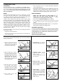
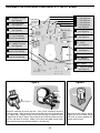
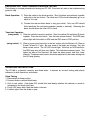
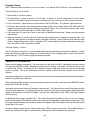
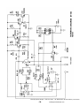
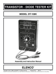
DIODE / TRANSISTOR TESTER KIT
MODEL DT-100K
99 Washington Street
Melrose, MA 02176
Phone 781-665-1400
Toll Free 1-800-517-8431
Visit us at www.TestEquipmentDepot.com
Assembly and Instruction Manual
Elenco Electronics, Inc.
®
DT-100 PARTS LIST
If you are a student, and any parts are missing or damaged, please see instructor or bookstore.
If you purchased this diode/transistor tester kit from a distributor, catalog, etc., please contact Elenco®
Electronics (address/phone/e-mail is at the back of this manual) for additional assistance, if needed. DO NOT
contact your place of purchase as they will not be able to help you.
RESISTORS
Qty.
r1
r2
r2
r1
r1
r1
r1
r2
r1
r1
r1
r1
Symbol
R14
R5, R6
R1, R10
R13
R7
R12
R8
R2, R3
R9
R11
R4
R15
Value
100Ω 5% 1/4W
220Ω 5% 1/4W
330Ω 5% 1/4W
1kΩ 5% 1/4W
5.6kΩ 5% 1/4W
10kΩ 5% 1/4W
18kΩ 5% 1/4W
33kΩ 5% 1/4W
47kΩ 5% 1/4W
100kΩ 5% 1/4W
330kΩ 5% 1/4W
100kΩ 5% 1/4W
Qty.
r1
r3
r2
Symbol
C6
C2, C3, C5
C1, C4
Value
.001μF (102)
.01μF (103)
10μF
Color Code
brown-black-brown-gold
red-red-brown-gold
orange-orange-brown-gold
brown-black-red-gold
green-blue-red-gold
brown-black-orange-gold
brown-gray-orange-gold
orange-orange-orange-gold
yellow-violet-orange-gold
brown-black-yellow-gold
orange-orange-yellow-gold
Variable
Part #
131000
132200
133300
141000
145600
151000
151800
153300
154700
161000
163300
192611
CAPACITORS
Description
Discap
Discap
Electrolytic
Part #
231036
241031
271045
SEMICONDUCTORS
Qty.
r1
r1
r4
r1
r5
Symbol
D1
Q5
Q1-Q4
IC1
L1-L5
Value
1N4001
MPS A70
2N3904
555
Qty.
r1
r1
r2
r1
r1
r1
r1
r5
r4
r4
r1
r1
r1
Description
PC Board
Switch Push Button
Switch DPDT
Battery Snap
Panel Front
Knob
Case
Spacer LED
Screw M3 x 0.5 x 5mm
Screw Self-Tapping
7mm Hex Pot Nut
8mm x 14mm Washer
Lockwasher 5/16”
Description
Diode
Transistor
Transistor
Integrated Circuit
LED (Light Emitting Diode)
Part #
314001
320070
323904
330555
350002
MISCELLANEOUS
Qty.
r1
r1
r1
r1
r1
r1
r 4”
r1
r1
r1
r1
r1
r1
Part#
511100
540001
541111
590098
614100
622009
623240
624111
640300
643652
644101
645101
646101
-1-
Description
Socket 8-Pin IC
Transistor Socket
Alligator Clip Black
Alligator Clip Red
Alligator Clip Green
Alligator Clip Yellow
Double Sided Tape
Wire Black 15”
Wire Red 15”
Wire Yellow 15”
Wire Green 15”
Wire Blue 3”
Solder Tube Lead-Free
Part #
664008
664500
680001
680002
680003
680004
740004
813110
813210
813410
813510
814620
9LF99
CONSTRUCTION
Introduction
• Turn off iron when not in use or reduce temperature setting when
using a soldering station.
The most important factor in assembling your DT-100K Diode /
Transistor Kit is good soldering techniques. Using the proper soldering
iron is of prime importance. A small pencil type soldering iron of 25 - 40
watts is recommended. The tip of the iron must be kept clean at all
times and well-tinned.
• Tips should be cleaned frequently to remove oxidation before it becomes
impossible to remove. Use Dry Tip Cleaner (Elenco® #SH-1025) or Tip
Cleaner (Elenco® #TTC1). If you use a sponge to clean your tip, then use
distilled water (tap water has impurities that accelerate corrosion).
Solder
Safety Procedures
For many years leaded solder was the most common type of solder
used by the electronics industry, but it is now being replaced by leadfree solder for health reasons. This kit contains lead-free solder, which
contains 99.3% tin, 0.7% copper, and has a rosin-flux core.
• Always wear safety glasses or safety goggles to
protect your eyes when working with tools or
soldering iron, and during all phases of testing.
• Be sure there is adequate ventilation when soldering.
Lead-free solder is different from lead solder: It has a higher melting
point than lead solder, so you need higher temperature for the solder to
flow properly. Recommended tip temperature is approximately 700OF;
higher temperatures improve solder flow but accelerate tip decay. An
increase in soldering time may be required to achieve good results.
Soldering iron tips wear out faster since lead-free solders are more
corrosive and the higher soldering temperatures accelerate corrosion,
so proper tip care is important. The solder joint finish will look slightly
duller with lead-free solders.
'
• Locate soldering iron in an area where you do not have to go around
it or reach over it. Keep it in a safe area away from the reach of
children.
• Do not hold solder in your mouth. Solder is a toxic substance.
Wash hands thoroughly after handling solder.
Assemble Components
In all of the following assembly steps, the components must be installed
on the top side of the PC board unless otherwise indicated. The top
legend shows where each component goes. The leads pass through the
corresponding holes in the board and are soldered on the foil side.
Use only rosin core solder.
Use these procedures to increase the life of your soldering iron tip when
using lead-free solder:
• Keep the iron tinned at all times.
• Use the correct tip size for best heat transfer. The conical tip is the
most commonly used.
DO NOT USE ACID CORE SOLDER!
What Good Soldering Looks Like
Types of Poor Soldering Connections
A good solder connection should be bright, shiny, smooth, and uniformly
flowed over all surfaces.
Soldering Iron
1. Solder all components from the
copper foil side only. Push the
soldering iron tip against both the
lead and the circuit board foil.
Rosin
Component Lead
1. Insufficient heat - the solder will
not flow onto the lead as shown.
Foil
Soldering iron positioned
incorrectly.
Circuit Board
2. Apply a small amount of solder to
the iron tip. This allows the heat to
leave the iron and onto the foil.
Immediately apply solder to the
opposite side of the connection,
away from the iron. Allow the
heated component and the circuit
foil to melt the solder.
3. Allow the solder to flow around
the connection. Then, remove
the solder and the iron and let the
connection cool. The solder
should have flowed smoothly and
not lump around the wire lead.
Soldering Iron
2. Insufficient solder - let the
solder flow over the connection
until it is covered.
Use just enough solder to cover
the connection.
Solder
Foil
Solder
Gap
Component Lead
Solder
3. Excessive solder - could make
connections that you did not
intend to between adjacent foil
areas or terminals.
Soldering Iron
Solder
Foil
4. Solder bridges - occur when
solder runs between circuit paths
and creates a short circuit. This is
usually caused by using too much
solder.
To correct this, simply drag your
soldering iron across the solder
bridge as shown.
4. Here is what a good solder
connection looks like.
-2-
Soldering Iron
Foil
Drag
ASSEMBLE THE FOLLOWING COMPONENTS TO THE PC BOARD
R4 - 330kΩ Resistor
(org-org-yel-gold)
R1 - 330Ω Resistor
(org-org-brn-gold)
J1 - Jumper Wire
(see Figure A)
R3 - 33kΩ Resistor
R2 - 33kΩ Resistor
(org-org-org-gold)
R5 - 220Ω Resistor
R6 - 220Ω Resistor
(red-red-brn-gold)
R9 - 47kΩ Resistor
(yel-vio-org-gold)
R13 - 1kΩ Resistor
(brn-blk-red-gold)
R8 - 18kΩ Resistor
(brn-gray-org-gold)
R12 - 10kΩ Resistor
(brn-blk-org-gold)
R7 - 5.6kΩ Resistor
(grn-blue-red-gold)
R11 - 100kΩ Resistor
(brn-blk-yel-gold)
R10 - 330Ω Resistor
(org-org-brn-gold)
R14 - 100Ω Resistor
(brn-blk-brn-gold)
SAVE 3 CUT-OFF
RESISTOR LEADS
Figure A
Figure B
Figure C
Jumper Wire
Flat
Form jumper wire
from a discarded
resistor lead.
Figure D
Flat
Spacer
Mount with the flat side of
LED as shown in the top
legend of the PC board.
Polarity
Mark
Mount with the flat side of the
transistor as shown on the top legend
of the PC board. Leave 1/8” between
the part and PC board.
Figure E
Insert the IC socket
into the PC board
with the notch in the
direction shown on
the
top
legend.
Solder the IC socket
into place. Insert the
IC into the socket with
the notch in the same
direction as the notch
on the socket.
(–)
(+)
Be sure that the positive lead is in the correct hole
as shown on the PC board. Bend the electrolytic
over and solder into place.
Warning: If the capacitor is connected with
incorrect polarity, it may heat up and either leak
or cause the capacitor to explode.
Band
Figure F
Notch
D1
Diodes have polarity, so be sure that the band is
in the correct direction, as shown on the top
legend of the PC board.
-3-
ASSEMBLE THE FOLLOWING COMPONENTS TO THE PC BOARD
L1
L4
L2
L5
L3
Q1 - 2N3904 Transistor
(see Figure B)
C1 - 10μF Electrolytic
(see Figure C)
Q5 - MPS A70 Transistor
(see Figure B)
- LED & Spacer
- LED & Spacer
- LED & Spacer
- LED & Spacer
- LED & Spacer
(see Figure D)
Q4 - 2N3904 Transistor
(see Figure B)
C3 - .01μF Capacitor
C2 - .01μF Capacitor
(may be marked 103)
C4 - 10μF Electrolytic
(see Figure C)
8-Pin IC Socket
IC1 - 555 IC
(see Figure E)
Q2 - 2N3904 Transistor
Q3 - 2N3904 Transistor
(see Figure B)
D1 - 1N4001 Diode
(see Figure F)
C6 - .001μF Capacitor
(may be marked 102)
SW2 - Switch
C5 - .01μF Capacitor
(may be marked 103)
R15 - 100k Pot
(see Figure G)
SW1 - Switch
S1 - Transistor Socket
(see Figure H)
Figure H
Figure G
Bare Wire
Key
Pad
Bend Tab Over
Bend the mounting tab on the pot over. Place a 5/16” lockwasher onto the
shaft of the pot. Insert the shaft of the pot into the hole in the PC board from
the copper side. Position the pot so that the three lugs are above the three
copper pads on the PC board. Secure the pot to the PC board with the 7mm
pot nut and 8mm flat washer. Solder a bare wire (discarded resistor lead)
from the pot lug to the pad directly below on all three lugs.
-4-
Match key on the socket to the top
legend on the PC board. Mount
with 3/16” of space between the
socket and PC board.
FINAL ASSEMBLY
r Install the push button switch to the front
panel in the hole marked “TEST”. Fasten
switch in place with the 1/4” nut. Tighten the
nut with pliers (be careful not to scratch the
panel).
Blue
r Strip the insulation off both ends of the blue
wire to expose 1/4” of bare wire. Solder one
end to the hole on the copper side of the PC
board, as shown in Figure I. Solder the other
end of the wire to a lug on the push button
switch.
Switch
Red
r Solder the red wire from the battery snap to
the other lug on the push button switch, as
shown in Figure I.
Black
Battery Snap
r Insert the black wire from the battery snap
into the pad on the PC board from the copper
side. Solder the wire in place, as shown in
Figure I.
Figure I
r Strip 1/4” insulation off both ends of the red wire. Insert one end into pad “D” on the copper side of
the PC board and solder the wire into place. Tie a knot 2 1/2” from soldered end of wire. Pull the
free end through the hole of the front panel marked “DIODE”, see Figure J.
r Strip 1/4” insulation off both ends of the black
wire and insert one end into pad “E” on the
copper side of the PC board and solder the
wire into place. Tie a knot 2 1/2” from the
soldered end of the wire. Pull the free end
through the hole of the front panel marked
“E”, see Figure J.
Figure J
r Strip 1/4” insulation off both ends of the yellow
wire and insert one end into pad “B” on the
copper side of the PC board and soldered end
of the wire. Pull the free end through the hole
of the front panel marked “B”, see Figure J.
D
B
E
C
Knot
r Strip 1/4” insulation off both ends of the green
wire and insert one end into pad “C” on the
copper side of the PC board and solder wire
into place. Tie a knot 2 1/2” from soldered
end of wire. Pull the free end through the hole
of the front panel marked “C”, see Figure J.
Red
“Diode”
-5-
Black
“E”
Yellow
“B”
Green
“C”
r Mount the front panel to the switches on the PC
board using four M3 x 0.5 x 5mm screws (see
Figure K).
r Remove the colored boots from the four alligator
clips (to remove the boots, clip the alligator clip onto
a pencil and slide the boot off). Slide each boot onto
the four corresponding colored wires (black boot
onto black wire, etc.).
M3 x 0.5 x
5mm Screws
Panel
r Solder an alligator clip to each wire as shown in
Figure L. Slide the boots back onto the clips.
PCB
r Turn the shaft of the base current control fully
counter-clockwise. Align the marker line on the
knob with “0” on the front panel, see Figure M. Push
the knob onto the shaft.
Figure K
r Cut two 2” pieces of double sided tape, peel off the
protective backing on one side and place next to
each other on the inside bottom of the case in the
position shown in Figure N.
r Obtain a 9 volt battery (alkaline preferred). Remove
the backing on the tape and mount the battery onto
the tape, as shown in Figure N.
Figure L
Bend tabs over wire
Clip
Boot
r Press the battery snap onto the battery terminals.
r Mount the assembled panel into the case, using four
self-tapping screws.
Figure M
Your transistor/diode tester is now completed and
ready for testing.
Figure N
Tape
9V
-6-
CHECKING OUT YOUR TRANSISTOR/DIODE TESTER
The following is a simple procedure for testing your DT-100. If the tests fail, refer to the troubleshooting
guide for help.
Diode Operation: 1.) Place the switch in the diode position. Short the black and red leads together
and push in the test button. The diode test LEDs should alternately go on at
about a 1Hz rate.
2.) Connect the red and black leads to any good diode. Only one LED should
flash identifying the red lead connection (anode or cathode). Reversing the
leads should cause the other LED to flash.
Transistor Operation:
(using leads) 1.) Place the switch in transistor position. Short the yellow (B) and black (E) leads
together. Press the test button. Vary the base current control. The NPN lamp
should light with the switch in NPN and the PNP when in PNP position.
(using socket) 2.) Place a known good transistor in the test socket with the Emitter in E, Base in
B and Collector in C pins. Be sure none of the leads are shorting. Vary the
base current control. The OK LED should light. Note that on NPN transistor,
the NPN lamp also will glow very slightly. This indicates the base current. The
higher the beta of the transistor, the lower the base current, and thus, lower
intensity. The base current control should be adjusted for the lowest setting with
the OK lamp glowing.
OPERATING INSTRUCTIONS
The DT-100 is a dynamic transistor and diode tester. It features an in-circuit testing and polarity
indicators for both transistors and diodes.
Diode Testing
1. Place switch in diode position.
2. Connect diode to red and black leads.
3. Push in test switch. One diode LED should blink and identify whether the cathode or anode is
connected to the diode (red) lead.
4. If both LED lamps blink, then the diode is shorted.
5. If neither lights, then the diode is open.
-7-
Transistor Testing
The DT-100 can measure transistors in or out of circuit. It will identify NPN or PNP by a simple adjustment.
Transistor testing - Out of Circuit
1. Place switch in transistor position.
2. Place transistor in socket or attach to C, B, E leads. If collector C, base B and emitter E are not known,
assume B is the center lead on small plastic transistors and C the metal case or tab on power transistors.
3. Push in test button. Adjust the base current control so that OK LED lights. This indicates a good transistor.
4. If OK lamp does not light, then adjust the base current control co that either NPN or PNP LED lights. This
happens at minimum or maximum position of the control setting. This will indicate transistor type. Place
switch to NPN if the NPN lamp lights, to PNP if PNP lamp is lit.
5. If no lamps light, the transistor is open or we have not identified the base lead. Repeat assuming another
lead as base.
6. When the transistor is shown to be OK, the base current control gives an indication of transistor beta. The
lower the setting relative to another transistor, the higher the beta. Lamps NPN and PNP measure base
current. Higher base current results in a brighter LED. It also indicates if current is entering or leaving the
base, thus NPN or PNP respectively will light.
Transistor Testing - In Circuit
The DT-100 will test transistors in circuit provided the base biasing resistance is greater than 100 ohms. Simply
follow the previous procedure for testing out of circuit transistors. Do not apply power to circuit of transistor or
diode under test. The DT-100 will supply the necessary power.
THEORY OF OPERATION
Note the circuit diagram on page 10. The test transistor in this circuit is a NPN. Adjusting the variable resistor
will cause the NPN LED to light, indicating that base current is flowing. The output of the test transistor is fed
to amplifier Q2 and Q3. The output of Q2 is fed back in phase to the base of the test transistor causing the
circuit to oscillate. Part of the oscillations are fed to a power rectifier Q5 which switches on the OK LED
indicator.
The design configuration is such that in-circuit transistors can be measured provided that the base and collector
resistors are greater than 100 ohms.
When measuring PNP transistors, the power supplied to the test transistor is reversed via the NPN/PNP switch,
therefore the PNP LED will light.
Varying the base current control will reduce the base current. The lower the base current, the higher the gain
of the transistor under test. Comparative tests of two transistors gain (beta) can be made by observing the dial
setting or the intensity of the base LED diode. The lower the setting with the PNP LED lit, the higher the beta
of that transistor.
On diode operation, power is applied to IC1. This causes the circuit to oscillate at about a 1Hz rate. Placing a
diode in series with the LED indicators will cause a current to flow depending on the direction of the diode. Thus,
the red test lead will identify the cathode or anode of the diode via the LED readout. Transistor Q4 reverses the
current flow in this circuit.
All types of diodes may be tested: Silicon, germanium, LEDs or zeners over 6 volts. Zener diodes under 6V
causes the second LED to glow at lower intensity, indicating that zener breakdown has occurred.
-8-
TROUBLESHOOTING GUIDE
If any problems occur, first check your wiring and soldering. Keep in mind that most problems are due
to poor soldering or wiring errors. Be sure that there are no solder shorts, poor connections or wiring
errors. Check that the battery is connected. Be sure that the transistors are in correctly. Check the
LEDs. The LED leads are hard to identify and can easily be wired backwards. The following is a guide
to help solve most problems.
Diode Position: Red and black leads shorted together. LEDs should alternately blink at 1Hz rate.
A. LEDs do not blink. Check that IC1 is in correctly. Check wiring around IC1.
B. Only one LED blinks. Check for open LED. Check transistor Q4.
C. Both LEDs blink together. One LED is in backwards.
Transistor Position Using Leads: B&E test leads shorted together. Rotate base current from
minimum to maximum. NPN LED should light up when switched to NPN and PNP LED should light
when in PNP position. OK LED should not light.
A. No LEDs light. Check that the battery is connected properly. Check for open circuit at R15, B or
E leads.
B. Only one LED lights. Check wiring and soldering. Check for open LED.
C. Both LEDs light at the same time. LED is in backwards.
Transistor Position Using Socket: Put the good NPN transistor into the test socket. Switch SW1 to
NPN position. Rotate base current control. The OK lamp should light. If not, check the following:
A.
B.
C.
D.
E.
No test leads are shorting together.
The NPN LED should be lit. If not, then refer to I.
Components around transistors Q1 to Q5 are in properly. Be sure no soldering errors exist.
Transistors are not in backwards.
Touch the collector of Q1 with the black (E) test leads. The OK LED should light. If not, then the
LED is either open or in backwards.
F. Look for a possible defective transistor or other component.
-9-
Test Equipment Depot - 800.517.8431 - 99 Washington Street Melrose, MA 02176
-10-
TestEquipmentDepot.com