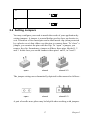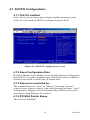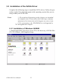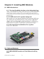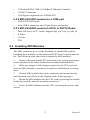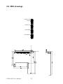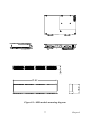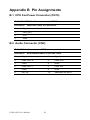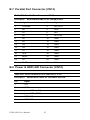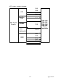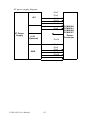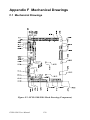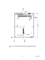
1
PCM-9386
Celeron® M 3.5" SBC with MIO/
VGA/LCD/LVDS Ethernet/USB2.0
and SSD
User Manual
Copyright
This document is copyrighted, © 2006. All rights are reserved. The original manufacturer reserves the right to make improvements to the products
described in this manual at any time without notice.
No part of this manual may be reproduced, copied, translated or transmitted in any form or by any means without the prior written permission of
the original manufacturer. Information provided in this manual is
intended to be accurate and reliable. However, the original manufacturer
assumes no responsibility for its use, nor for any infringements upon the
rights of third parties that may result from such use.
Acknowledgements
Award is a trademark of Award Software International, Inc.
VIA is a trademark of VIA Technologies, Inc.
IBM, PC/AT, PS/2 and VGA are trademarks of International Business
Machines Corporation.
Intel, Pentium, Celeron, and MMX are registered trademarks of Intel Corporation.
Microsoft Windows® is a registered trademark of Microsoft Corp.
RTL is a trademark of Realtek Semi-Conductor Co., Ltd.
ESS is a trademark of ESS Technology, Inc.
UMC is a trademark of United Microelectronics Corporation.
SMI is a trademark of Silicon Motion, Inc.
Creative is a trademark of Creative Technology LTD.
All other product names or trademarks are properties of their respective
owners.
For more information on this and other Advantech products, please visit
our websites at:
http://www.advantech.com
http://www.advantech.com/eplatform
For technical support and service, please visit our support website at:
http://www.advantech.com/support
This manual is for the PCM-9386.
Part No. 2006938612
3rd Edition
Printed in Taiwan
Nov. 2006
PCM-9386 User Manual
ii
Packing List
Before you begin installing your card, please make sure that the following
materials have been shipped:
• 1 PCM-9386 SBC
• 1 Startup manual
• 1 Utility CD
• 1 mini jumper pack
p/n: 9689000002
• 1 Audio cable
p/n: 1703100152
• 1 IDE 44 pin cable
p/n: 1701440351
• 1 USB 2 port Cable
p/n: 1703100121
• 1 Parallel port cable
p/n: 1700260250
• 1 Keyboard/Mouse cable
p/n: 1700060202
• 1 FDD adapter for slim FDD and FDD p/n: 9681000044
• 1 Cable for Slim FDD
p/n: 1701260125
• 1 Flat cable for FDD
p/n: 1701340700
• 1 embedded COM port cable
p/n: 1701140201
• 1 ATX power cable 20P-12P cable p/n: 1700000265
If any of these items are missing or damaged, contact your distributor or
sales representative immediately.
Model No. List
Description
• PCM-9386F-M0A2E 3.5" SBC with ULV Celeron M 600 MHz (0 L2)
VGA, LVDS, LAN, USB
• PCM-9386F-S0A2E 3.5" SBC with ULV Celeron M 1.0 GHz (0 L2)
VGA, LVDS, LAN, USB
• PCM-9386S-50A2E PCM-9386F-S0A2E w/MIO-6250, XPe
OS,512MB CF, 512MB RAM
• PCM-9386S-54A2E PCM-9386F-S0A2E w/MIO-6254, XPe
OS,512MB CF, 512MB RAM
iii
Additional Information and Assistance
1.Visit the Advantech web site at www.advantech.com where you can
find the latest information about the product.
2.Contact your distributor, sales representative, or Advantech's customer
service center for technical support if you need additional assistance.
Please have the following information ready before you call:
•Product name and serial number
•Description of your peripheral attachments
•Description of your software (operating system, version, application
software, etc.)
•A complete description of the problem
•The exact wording of any error messages
PCM-9386 User Manual
iv
This device complies with the requirements in part
15 of the FCC rules: Operation is subject to the following two conditions:
1.This device may not cause harmful interference,
and
2.This device must accept any interference
received, including interference that may cause
undesired operation
This equipment has been tested and found to comply with the limits for a Class A digital device, pursuant to Part 15 of the FCC Rules. These limits are
designed to provide reasonable protection against
harmful interference when the equipment is operated in a commercial environment. This equipment
generates, uses, and can radiate radio frequency
energy and, if not installed and used in accordance
with the instruction manual, may cause harmful
interference to radio communications. Operation of
this device in a residential area is likely to cause
harmful interference in which case the user will be
required to correct the interference at his/her own
expense. The user is advised that any equipment
changes or modifications not expressly approved
by the party responsible for compliance would void
the compliance to FCC regulations and therefore,
the user's authority to operate the equipment.
Caution!
Achtung!
There is a danger of a new battery exploding if it is
incorrectly installed. Do not attempt to recharge,
force open, or heat the battery. Replace the battery
only with the same or equivalent type recommended by the manufacturer. Discard used batteries according to the manufacturer’s instructions
v
PCM-9386 User Manual
vi
Contents
Chapter
1 Introduction ......................................................2
1.1
1.2
1.3
Introduction ....................................................................... 2
Features ............................................................................. 2
Specifications .................................................................... 3
1.3.1
1.3.2
1.3.3
1.3.4
1.3.5
1.4
Standard 3.5" Biscuit SBC Functions............................. 3
VGA/LVDS Interface ..................................................... 3
Ethernet Interface............................................................ 4
Audio Function ............................................................... 4
Mechanical and Environmental ...................................... 4
Board layout: dimensions.................................................. 5
Figure 1.1:Board layout: Dimensions (Component Side)
.............................................................................5
Figure 1.2:Board layout: Dimensions (Solder Side)....... 6
Chapter
2 Installation ........................................................8
2.1
Jumpers.............................................................................. 8
2.1.1
Jumper Location ............................................................ .8
Table 2.1:Jumpers........................................................... 8
Table 2.2:Audio Power Selector(J1)............................... 9
Table 2.3:COM2 Mode Setting(J3/J4/J5)....................... 9
Table 2.4:LCD Power Setting (J6) ................................. 9
Table 2.5:Audio Enable/Disable (J7).............................. 9
Table 2.6:AT/ATX Power Setting (J8)........................... 9
Table 2.7:CMOS clear .................................................. 10
2.2
Connectors....................................................................... 11
2.3
Locating Connectors ........................................................... 12
Table 2.8:Connectors .................................................... 11
Figure 2.1:Connectors (component side)...................... 12
Figure 2.2:Connectors (solder side).............................. 12
2.4
2.5
2.6
Setting Jumpers ............................................................... 17
Installing SO-DIMM ....................................................... 18
IDE, CDROM hard drive connector (CN6) .................... 18
2.6.1
2.7
2.7.1
2.8
CompactFlash (CN21) .................................................. 19
Floppy Disk Drive connector (CN20)............................. 19
2.8.1
2.9
2.10
2.11
Connecting the hard drive............................................. 19
Solid State Disk............................................................... 19
Connecting the floppy disk drive.................................. 19
Parallel port connector (CN13) ....................................... 20
Keyboard and PS/2 mouse connector (CN14) ................ 20
Power & HDD LED Connector (CN10) ......................... 21
2.11.1 Power & HDD LED Connector(CN10)........................ 21
vii
2.11.2 Power Reset button (S2) ............................................... 21
2.12
Power connectors (CN3) ................................................. 21
2.12.1 Main power connector, +5 V, +12 V (CN3)................. 21
2.12.2 Fan power supply connector (CN15)............................ 21
2.13
Audio interfaces (CN2) ................................................... 21
2.13.1 Audio connector (CN2) ................................................ 21
2.14
COM port connector (CN8,CN19).................................. 21
2.14.1 COM2 RS-232/422/485 setting (J3/J4/J5).................... 22
Table 2.9: J3/J4/J5: COM2 RS-232/422/485 select...... 22
2.15
VGA/LCD/LVDS interface connections ........................ 22
2.15.1 CRT display connector (CN18) .................................... 22
2.15.2 LVDS LCD panel connector (CN1) ............................. 22
2.16
Ethernet configuration..................................................... 22
2.16.1 100Base-T/1000Base-T connector (CN12) .................. 22
2.16.2 Network boot (Depends on Ethernet Controller).......... 23
2.17
2.18
2.19
2.20
2.21
Watchdog timer configuration ........................................ 23
USB connectors (CN5,CN9) ........................................... 23
GPIO (General Purpose Input Output) (CN7)................. 23
MIO Connector (CN4) .................................................... 23
SMBus connector (default); SIR (optional) (CN11) ....... 24
2.21.1 SMBus .......................................................................... 24
2.21.2 SIR ............................................................................... 24
Chapter
3 Chipset Software Installation Utility............26
3.1
3.2
3.3
Chapter
Before you begin ............................................................. 26
Introduction ..................................................................... 26
Installing the CSI Utility ................................................. 27
4 Award BIOS Setup.........................................32
4.1
Introduction ..................................................................... 32
4.1.1
CMOS RAM Auto-backup and Restore ....................... 32
4.2
Entering Setup ................................................................. 33
4.3
Standard CMOS Setup .................................................... 34
4.4
Advanced BIOS Features ................................................ 35
Figure 4.1:Award BIOS Setup initial screen ................ 33
Figure 4.2:Standard CMOS features screen ................. 34
4.4.1
4.4.2
4.4.3
4.4.4
4.4.5
4.4.6
4.4.7
4.4.8
PCM-9386 User Manual
Figure 4.3:Advanced BIOS features screen.................. 35
Virus Warning............................................................... 35
L1 & L2 Cache ............................................................. 35
Quick Power On Self Test ............................................ 35
First/Second/Third/Other Boot Device......................... 36
Swap Floppy Drive ....................................................... 36
Boot UP Floppy Seek ................................................... 36
Boot Up NumLock Status............................................. 36
Gate A20 Option........................................................... 36
viii
4.4.9
4.4.10
4.4.11
4.4.12
4.4.13
4.4.14
4.5
Integrated Peripherals...................................................... 37
4.5.1
4.5.2
4.5.3
4.5.4
4.5.5
4.5.6
4.5.7
4.5.8
4.5.9
4.5.10
4.5.11
4.5.12
4.5.13
4.5.14
4.5.15
4.5.16
4.5.17
4.5.18
4.6
IDE Master/Slave PIO/UDMA Mode,.......................... 37
On-Chip Secondary PCI IDE........................................ 38
Figure 4.4:Integrated peripherals.................................. 38
USB Controller ............................................................. 38
USB Keyboard/Mouse Support .................................... 38
AC97 Audio.................................................................. 38
Init Display First ........................................................... 38
Onboard LAN Control .................................................. 38
IDE HDD Block Mode ................................................. 39
Onboard FDC Controller .............................................. 39
Onboard Serial Port ...................................................... 39
UART Mode Select ...................................................... 39
RxD, TxD Active.......................................................... 39
IR Transmission Delay ................................................. 39
UR2 Duplex Mode........................................................ 39
Onboard Parallel Port.................................................... 39
Parallel Port Mode ........................................................ 39
EPP Mode Select .......................................................... 40
ECP Mode Use DMA ................................................... 40
Power Management Setup............................................... 40
4.6.1
4.6.2
4.6.3
4.6.4
4.6.5
4.6.6
4.6.7
4.6.8
4.6.9
4.6.10
4.6.11
4.6.12
4.6.13
4.6.14
4.7
Typematic Rate Setting................................................. 36
Typematic Rate (Chars/Sec) ......................................... 36
Typematic Delay (msec)............................................... 36
Security Option ............................................................. 36
APIC Mode ................................................................... 37
MPS Version Control For OS....................................... 37
Figure 4.5:Power management setup screen................. 40
Power-Supply Type ...................................................... 40
ACPI function ............................................................... 40
Power Management ...................................................... 41
Video Off In Suspend ................................................... 41
Modem Use IRQ........................................................... 41
HDD Power Down........................................................ 41
Soft-Off by PWR-BTTN .............................................. 41
CPU THRM-Throttling................................................. 41
PowerOn By LAN ........................................................ 41
PowerOn By Modem .................................................... 42
PowerOn By Alarm ...................................................... 42
Primary IDE 0 (1) and Secondary IDE 0 (1) ................ 42
FDD, COM, LPT PORT ............................................... 42
PCI PIRQ [A-D]# ......................................................... 42
PnP/PCI Configurations .................................................. 43
4.7.1
PnP OS Installed ........................................................... 43
Figure 4.6:PnP/PCI configurations screen.................... 43
ix
4.7.2
4.7.3
4.7.4
4.8
4.9
4.10
Chapter
Password Setting ............................................................. 44
Save & Exit Setup ........................................................... 44
Exit Without Saving ........................................................ 45
5 PCI SVGA/LCD Setup ..................................48
5.1
Introduction ..................................................................... 48
5.1.1
5.1.2
5.1.3
5.2
5.2.2
5.3
Introduction ..................................................................... 58
Driver installation............................................................ 58
6.2.1
6.2.2
Before you begin........................................................... 58
Windows 98 drivers ...................................................... 59
7 Ethernet Interface ..........................................62
7.1
7.2
Introduction ..................................................................... 62
Installation of Ethernet driver ......................................... 62
7.2.1
7.2.2
7.3
Chapter
Installation of Windows 98/2000.................................. 52
Further Information ......................................................... 55
6 Audio Setup.....................................................58
6.1
6.2
Chapter
LG LM 150x06 (1024x768 LVDS LCD) ..................... 50
Table 5.1:Connections to LCD/Flat Panel (CN1)......... 50
AU M170EG01 (1280x1024 TFT LCD @ 48bit) ........ 51
Table 5.2:Connections to AU M170EG01 (CN1) ........ 51
Installation of the SVGA Driver ..................................... 52
5.3.1
5.4
CMOS setting for panel type ........................................ 48
Display type .................................................................. 48
Dual Independent Display ............................................ 48
Connections to Two Standard LCDs............................... 50
5.2.1
Chapter
Reset Configuration Data.............................................. 43
Resources controlled by:............................................... 43
PCI/VGA Palette Snoop ............................................... 43
Installation for Windows 98 ......................................... 62
Installation for Windows 2000 ..................................... 66
Further information ......................................................... 71
8 Installing MIO Modules ................................74
8.1
MIO Introduction ............................................................ 74
8.1.1
8.1.2
8.1.3
8.2
The best flexibility interface in the Embedded App ..... 74
A SBC short cut to system design-win ......................... 74
The best board combination for a system ..................... 74
Optional Modules............................................................ 74
8.2.1
MIO-6250 MIO module w/3 Fast Ethernet with by pass .
..........................................................................................74
8.2.2 MIO-6253 MIO module for 4 COM port ..................... 75
8.2.3 MIO-6254 MIO module for DVO to DVI/TV/Audio .. 75
8.3
8.4
Installing MIO Modules .................................................. 75
MIO drawings ................................................................. 76
PCM-9386 User Manual
x
Figure 8.1:MIO module mounting diagram.................. 77
Table 8.1:MIO connectors ............................................ 78
Appendix A Programming GPIO & Watchdog Timer ....82
A.1
Supported GPIO Register................................................ 82
A.1.1
A.1.2
A.2
GPIO Registers ............................................................. 82
GPIO Example program-1 ............................................ 83
Watchdog programming.................................................. 85
Appendix B Pin Assignments .............................................88
B.1
CPU Fan Power Connector (CN15) ................................ 88
B.2
Audio Connector (CN2) .................................................. 88
B.3
Main Power Connector (CN3) ........................................ 89
B.4
Keyboard and PS/2 Mouse Connector (CN14) ............... 89
B.5
Floppy Disk Drive Connector (CN20) ............................ 90
B.6
IDE Hard Drive Connector (CN6) .................................. 91
B.7
Parallel Port Connector (CN13) ..................................... 92
B.8
Power & HDD LED Connector (CN10) ......................... 92
B.9
USB Connector (CN5) .................................................... 93
B.10
LCD Inverter Backlight Connector (CN17).................... 93
B.11
LVDS Connector (CN1).................................................. 94
B.12
COM2 RS232/422/485 series port (CN8)....................... 95
Table B.1:CPU Fan Power connector (CN15).............. 88
Table B.2:Audio connector (CN2)................................ 88
Table B.3:Main Power Connector (CN3) ..................... 89
Table B.4:Keyboard and mouse connector (CN14)...... 89
Table B.5:Floppy Disk Drive Connector (CN20)......... 90
Table B.6:IDE HDD connector (CN6) ......................... 91
Table B.7:Parallel Port Connector (CN13)................... 92
Table B.8:Power & HDD LED Connector (CN10)...... 92
Table B.9:USB Connector (CN5)................................. 93
Table B.10:LCD Inverter Backlight Conn. (CN17) ..... 93
Table B.11:LVDS Connector (CN1) ............................ 94
Table B.12:COM2 RS-232/422/485 series port ........... 95
B.12.1 CN8, COM2 RS422/485 - transfer to 2nd internal RS-232
..........................................................................................95
B.12.2 CN8, 2nd internal RS-232 - transfer to COM2 RS-422/
485....................................................................................95
B.13
CompactFlash Card Connector (CN21) ......................... 96
B.14
SMBus Connector (default); IrDA (optional) (CN11) .... 97
Table B.13:CompactFlash Card Connector (CN21)..... 96
Table B.14:SMBUS connector (Default); IrDA connector
(Optional) (CN11).............................................97
B.15
MIO interface (CN4)...................................................... .97
Table B.15:MIO connectors ......................................... 97
xi
B.16
GPIO Connector (CN7)................................................. 101
B.17
USB2 Connector (CN9) ................................................ 101
B.18
Print Port (CN13) .......................................................... 102
Table B.16:GPIO connector (CN7) ............................ 101
Table B.17:USB2 connector (CN9)............................ 101
Table B.18:Print Port (CN13)..................................... 102
Appendix C
System Assignments ....................................104
C.1
System I/O Ports............................................................ 104
C.2
1st MB memory map..................................................... 105
C.3
DMA channel assignments............................................ 106
C.4
Interrupt assignments .................................................... 107
Table C.1:System I/O ports ........................................ 104
Table C.2:1st MB memory map ................................. 105
Table C.3:DMA channel assignments ........................ 106
Table C.4:Interrupt assignments ................................. 107
Appendix D AT/ATX Power setting ................................110
D.1
Introduction ................................................................... 110
Table D.1:Power Connector ....................................... 110
Appendix E Optional Kit ..................................................116
E.1 Embedded OS................................................................ 116
E.2 Optional Kit................................................................... 116
E.3 Assembly for CPU and cooling for PCM-9386, uFCPGA
type CPU, please follow the following assembly information...116
Appendix F Mechanical Drawings...................................120
F.1
Mechanical Drawings.................................................... 120
Figure F.1:PCM-9380/9386 Mech Drawing (Component)
.........................................................................120
Figure F.2:PCM-9380/9386 Mech Drawing (Solder Side)
.........................................................................121
PCM-9386 User Manual
xii
CHAPTER
1
General Information
This chapter gives background information on the PCM-9386.
Sections include:
• Introduction
• Features
• Specifications
• Board layout and dimensions
Chapter 1 Introduction
1.1 Introduction
The PCM-9386 is a 3.5” SBC (Single Board Computing) with a high performance and lower power based on Celeron M processors.
The PCM-9386, in conjunction with Intel 852GM chipset and Intel CPU
Celerom M 600MHz (with 0 L2 cache), or Celeron M 1.0GHz (with
512K L2 cache), supports three USB 2.0 compatible ports, a PCI Fast or
Gigabit (optional). Ethernet interface, 2 Channel LVDS interface, and one
MIO expansion connector, and accommodate up to 1GB of DDR RAM
memory.
The PCM-9386’s board can be easier stacking on series MIO modules for
different application market requirement.
MIO (module I/O) is an open pin definition from Advantech. MIO interface integrate the most popular interface in the world in a high-density
160-pin connector, these popular interface include, integrated PCI 2.0,
LPC, USB2.0, SMBus, AC97 and DVO bus. With MIO (module I/O)
interface can do the great help a board level engineer to speed up the system project design. More details describe in Appendix B.
1.2 Features
• Embedded Intel ULV Celeron M 600MHz Processor or ULV Celeron M 1.0GHz Processor
• Supports DDR memory
• Supports 1000Base-T Ethernet
• Supports 2 channel 2 x18-bit LVDS LCD display (2 x 24-bit
optional)
• Supports 3 x USB 2.0 port
• Supports MIO expansion
PCM-9386 User Manual
2
1.3 Specifications
1.3.1 Standard 3.5" Biscuit SBC Functions
• CPU:Embedded Intel ULV Celeron M 600 MHz (512k L2 cache)
Embedded Intel ULV Celeron M 1.0 GHz (0 L2 cache)
• System Memory: 1x SODIMM socket, supports Double Data Rate
(DDR) 128 MB to 1GB, accepts 128/256/512/1000 MB DDR200/
266 DRAM
• 2nd Cache Memory: Depends on CPU type from 0 to 512KB
• System Chipset: Intel 852GM GMCH/ICH4 chipset
• BIOS: AWARD 4Mbit Flash BIOS
• Watchdog timer: 255 levels timer interval
• Expansion Interface: MIO Interface, integrated PCI 2.0, LPC,
USB2.0, SMBus, AC97 and DVO Bus.
• Battery: Lithium 3V/196 mAH
• Power management: Supports power saving modes, including Normal/
Standby/Suspend modes. APM 1.2, ACPI compliant, wake on LAN,
and modem ring-in functions
• Enhanced IDE interface: One channel supports up to
four EIDE devices. BIOS auto-detect, PIO Mode 3 or
Mode 4, supports UDMA 33 mode
• FDD Interface: Supports up to one FDD
• Serial ports: Two serial RS-232 ports, COM1: RS-232,
COM2: RS-232/422/485 (2nd internal RS-232 optional)
• Parallel port: One parallel port, supports SPP/EPP/ECP mode
• Keyboard/mouse connector: Supports one standard PC/AT keyboard
and a PS/2 mouse
• Audio: Supports AC97 Audio stereo sound
• USB: Three USB 2.0 compliant universal serial bus ports
• Solid State Disk (SSD): Supports one 50-pin socket for CFC type I/II
• IrDA: 115kbps, SIR, IrDA 1.0 complaint (optional)
• GPIO: 8 bit general purpose Input / Output
• SMBus: System Management Bus for advanced monitoring/control
interface
1.3.2 VGA/LVDS Interface
• Chipset: Intel 852GM Graphic Memory Control Hub (GMCH)
• Memory Size: Optimized Shared Memory Architecture, supports 64MB frame
buffer using system memory
• Resolution: CRT display Mode: pixel resolution up to 1600 x 1200
@85-Hz
3
Chapter 1
• LVDS Interface: Up to UXGA panel resolution with frequency range
from 25MHz to 112MHz
• TTL LCD: optional, supported by PCM-3540R module
• LVDS LCD: Supports 2 channel 2 x 18-bits LVDS LCD Panel (2 x 24bit optional), 16:9 wide screen panel supported
• TV-out: optional, by MIO-6254 module
• Dual Independent Display: Supports three dual independent mode:
CRT+LVDS
CRT + DVI (w/MIO-6254)
LVDS + DVI (w/MIO-6254)
1.3.3 Ethernet Interface
• Chipset supports: Intel 82551QM (10/100Mbps) (with Wake on LAN)
10/100/1000Mbps - Intel 82541PI (Optional)
• Interface: RJ45 connector
• Standard IEEE 802.3 z/ab (1000BASE-T) or IEEE 802.3u
(100 BASE-T) protocol compatible
• Built-in boot ROM.
1.3.4 Audio Function
• Chipset: IntelR 82801DB I/O Controller Hub 4 (ICH4) & ALC203
codec chipset
• Audio controller: Supports AC97 3D Audio stereo sound
• Audio interface: Microphone in, line in, line out
1.3.5 Mechanical and Environmental
• Dimensions: 145 x 102 mm (5.9"x 4.2")
Mechanical Drawing (dxf file) is available.
• Power Supply Type: AT/ATX
• Power Requirement: +5V ±5%, +12V ±5% (Optional), +5V standby
for ATX mode, or supports single +5V power only
• Power Consumption:
(ULV Celeron M 600 MHz @ 256 MB DDR266)
Max (HCT): +5 V @ 2.0 A, +12 V @ 0.02 A
• Operating temperature: 0 ~ 60°C (32 ~ 140°F)
• Operating Humidity: 10% ~ 90% relative humidity, non-condensing
• Weight: 0.85 kg (reference weight of total package)
PCM-9386 User Manual
4
1.4 Board layout: dimensions
Figure 1.1: Board layout: Dimensions (Component Side)
5
Chapter 1
Figure 1.2: Board layout: Dimensions (Solder Side)
PCM-9386 User Manual
6
CHAPTER
2
Installation
This chapter explains the setup procedures of the PCM-9386 hardware,
including instructions on setting jumpers and connecting peripherals,
switches and indicators. Be sure to read
all safety precautions before you begin
the installation procedure.
Chapter 2 Installation
2.1 Jumpers
The PCM-9386 has a number of jumpers that allow you to configure your
system to suit your application. The table below lists the functions of the
various jumpers.
2.1.1 Jumper Location
J7
J8
J6
J1
S1
J3
J5
J4
Table 2.1: Jumpers
Label
Function
J1
Audio Power Source
J3/J4/J5
COM2 Setting
J6
LCD Power Setting
J7
Audio Enable/Disable
J8
AT/ATX Power Setting
S1
Clear CMOS
S2
Reset button
PCM-9386 User Manual
8
Jumper Settings
Table 2.2: Audio Power Selector(J1)
Setting
Function
1-2(default)
2-3
Audio Power form 12V
Audio Power from 5V
Table 2.3: COM2 Mode Setting(J3/J4/J5)
Setting
Function
J3(1-2)(default) RS232
J4(1-2)
RS422
J5(1-2)
RS485
Table 2.4: LCD Power Setting (J6)
Setting
Function
1-2
2-3(default)
+5V
+3.3V
Table 2.5: Audio Enable/Disable (J7)
Setting
Function
Open(default)
Close
Enable
Disable
Table 2.6: AT/ATX Power Setting (J8)
Setting
Function
Open
AT Power (*)
Close(default)
ATX Power
* While use AT power, the standby power connector should be connected to 5V.
9
Chapter 2
Warning!
To avoid damaging the computer, always turn
off the power supply before setting “Clear
CMOS.” Before turning on the power supply,
set the jumper back to “3.0 V Battery On.”
This jumper is used to erase CMOS data and reset system BIOS information.
The procedure for clearing CMOS is:
1.
Turn off the system.
2.
Short pin 2 and pin 3.
3.
Return jumper to pins 1 and 2.
4.
Turn on the system. The BIOS is now reset to its default setting
Table 2.7: CMOS clear
Condition
Result
unpressed*
Normal
pushed
Clear CMOS
* default setting
PCM-9386 User Manual
10
2.2 Connectors
On-board connectors link the PCM-9386 to external devices such as hard
disk drives, a keyboard, or floppy drives. The table below lists the function of each of the board’s connectors.
Table 2.8: Connectors
Label
Function
CN1
LVDS Connector
CN2
Audio Connector
CN3
Power Connector
CN4
MIO Connector
CN5
Internal USB Connector (Channel 0,1) USB0/1 Connector
CN6
Primary IDE Connector
CN7
GPIO Connector
CN8
COM2 Connector
CN9
External USB Connector (Channel2) Connector
CN10
HD LED & Power LED Connector
CN11
SMBus connector (Optional: SIR)
CN12
LAN Connector
CN13
Print Port Connector
CN14
Keyboard /Mouse Connector
CN15
Fan Power Connector
CN16
Power Switch Connector
CN17
Inverter Power Connector
CN18
CRT Connector
CN19
COM1 Connector
CN20
Floppy Disck Drive (FDD) Connector
CN21
CF Connector
11
Chapter 2
2.3 Locating Connectors
Figure 2.1: Connectors (component side)
Figure 2.2: Connectors (solder side)
PCM-9386 User Manual
12
In order to configure each connector easily see Fig.2.1 and Fig 2.2 connector drawings with detailed pin numbers and locations.
Location
Dimension
CN1
2
31
CN2
3 1
2
CN3
3
1
2
CN4
CN5
1
3
13
2
Chapter 2
CN6
1
3
2
CN7
CN8
2
1 3
CN9
32 1
CN10
1
2
3
CN11
3
2
1
PCM-9386 User Manual
14
CN12
4
2
3
1
CN13
2
1 3
CN14
6 4 2 1 3 5
CN15
3
2
1
CN16
1
2
CN17
1
3
2
CN18
5 14 9 3 12 7 1
17 1510 4 13 8 2 11 6
15
16
Chapter 2
CN19
10
1
6
2
7
3
8
4
9
5
11
CN21
282726
32 1
J1
3
2
1
J2
2
1 3
J3/J4/J5
J6
3
2
1
PCM-9386 User Manual
16
J7
2
1
2
1
J8
2.4 Setting Jumpers
You may configure your card to match the needs of your application by
setting jumpers. A jumper is a metal bridge used to close an electric circuit. It consists of two metal pins and a small metal clip (often protected
by a plastic cover) that slides over the pins to connect them. To “close” a
jumper, you connect the pins with the clip. To “open” a jumper, you
remove the clip. Sometimes a jumper will have three pins, labeled 1, 2
and 3. In this case you would connect either pins 1 and 2, or 2 and 3.
open
closed
closed 2-3
The jumper settings are schematically depicted in this manual as follows:.
open
closed
closed 2-3
A pair of needle-nose pliers may be helpful when working with jumpers.
17
Chapter 2
If you have any doubts about the best hardware configuration for your
application, contact your local distributor or sales representative before
you make any changes.
Generally, you simply need a standard cable to make most connections.
2.5 Installing SO-DIMM
Module Key Aligned
With housing Key
2
Housing
Card Slot
PC Board
1
Module Tilted
Approximately 25
3
Module Latching
Ledge(TO Engage
Edge of Module)
The procedures for installing SODIMMs are described below. Please follow these steps carefully. You can install SDRAM memory modules
using 200-pin SODIMMs (Small Outline Dual In-line Memory Modules).
1.
Ensure that all power supplies to the system are switched off.
2.
Tilt the SODIMM card approximately 25o above the board, and
move it in the direction of the housing card slot. Make sure that the key in
the module and the key in the housing are aligned.
3.
Push the module into the socket until the module bottoms. There
should be a slight insertion force to engage the module into the contacts.
2.6 IDE, CDROM hard drive connector (CN6)
The board provides 1 IDE channels which you can attach up to two
Enhanced Integrated Device Electronics hard disk drives or CDROM to
the board’s internal controller. Its IDE controller uses a PCI interface.
PCM-9386 User Manual
18
This advanced IDE controller supports faster data transfer, PIO mode 3,
mode 4 and up to UDMA/33.
2.6.1 Connecting the hard drive
Connecting drives is done in a daisy-chain fashion. This package includes
One 44PIN IDE cable that can connect to 1.8" and 2.5" drives.
1.
Connect one end of the cable to Hard Drive connector. Make sure
that the red (or blue) wire corresponds to pin 1 on the connector,
which is labeled on the board (on the right side).
2.
Plug the other end of the cable into the Enhanced IDE hard drive,
with pin 1 on the cable corresponding to pin 1 on the hard drive.
(See your hard drive’s documentation for the location of the connector.)
If desired, connect a second drive as described above.
Unlike floppy drives, IDE hard drives can connect to either end of the
cable. If you install two drives, you will need to set one as the master and
one as the slave by using jumpers on the drives. If you install only one
drive, set it as the master.
2.7 Solid State Disk
The board provides a CompactFlash™ card type I/II socket.
2.7.1 CompactFlash (CN21)
The CompactFlash card shares a secondary IDE channel which can be
enabled/disabled via the BIOS settings.
2.8 Floppy Disk Drive connector (CN20)
You can attach up to two floppy drives to the board. You can use 3.5”
(720 KB, 1.44 MB, and 2.88 MB) drives.
A 26-pin FPC connector cable is required for a dual-drive system. On one
end of the cable is a 26-pin FPC-cable connector. On the other end are
two sets of floppy disk drive connectors. Each set consists of a 26-pin
FPC-cable connector (usually used for 3.5” drives).
2.8.1 Connecting the floppy disk drive
1.
Plug the 26-pin FPC-cable the board’s Floppy drive connector.
Make sure that the red wire corresponds to pin one on the connector.
19
Chapter 2
2.
Attach the appropriate connector on the other end of the cable to
the floppy drive(s). You can use only one connector in the set. The
set on the end (after the twist in the cable) connects to the A: drive.
The set in the middle connects to the B: drive.
If you are connecting a 3.5” floppy drive, you may have trouble determining which pin is number one. Look for a number printed on the circuit
board indicating pin number one. In addition, the connector on the floppy
drive may have a slot. When the slot is up, pin number one should be on
the right. Check the documentation that came with the drive for more
information.
If you desire, connect the B: drive to the connectors in the middle of the
cable as described above.
In case you need to make your own cable, you can find the pin assignments for the board’s connector in Appendix C.
2.9 Parallel port connector (CN13)
Normally, the parallel port is used to connect the card to a printer. The
board includes a multi-mode (ECP/EPP/SPP) parallel port accessed via
CN13 and a 26-pin flat-cable connector. You will need an adapter cable if
you use a traditional DB-25 connector. The adapter cable has a 26-pin
connector on one end, and a DB-25 connector on the other.
The parallel port is designated as LPT1, and can be disabled or changed to
LPT2 or LPT3 in the system BIOS setup.
The parallel port interrupt channel is designated to be IRQ7.
You can select ECP/EPP DMA channel via BIOS setup.
2.10 Keyboard and PS/2 mouse connector (CN14)
The board provides a keyboard connector that supports both a keyboard
and a PS/2 style mouse. In most cases, especially in embedded applications, a keyboard is not used. If the keyboard is not present, the standard
PC/AT BIOS will report an error or fail during power-on self-test (POST)
after a reset. The board’s BIOS standard setup menu allows you to select
“All, But Keyboard” under the “Halt On” selection. This allows no-keyboard operation in embedded system applications, without the system
halting under POST.
PCM-9386 User Manual
20
2.11 Power & HDD LED Connector (CN10)
Next, you may want to install external switches to monitor and control the
board. These features are optional: install them only if you need them.
The Power & HDD LED connector is 6-pin Wafer box connector. It provides connections for a power and hard disk access indicator.
2.11.1 Power & HDD LED Connector(CN10)
The HDD LED indicator for hard disk access is an active low signal (24
mA sink rate). Power supply activity LED indicator.
2.11.2 Power Reset button (S2)
Momentarily pressing the reset button will activate a reset. The switch
should be rated for 10 mA, 5 V.
2.12 Power connectors (CN3)
2.12.1 Main power connector, +5 V, +12 V (CN3)
Supplies main power to the PCM-9386 (+5 V), and to devices that require
+12 V.
2.12.2 Fan power supply connector (CN15)
Provides +5V power supply to CPU cooling fan.
2.13 Audio interfaces (CN2)
2.13.1 Audio connector (CN2)
The board provides all major audio signals on a 10-pin cable connector,
These audio signals include Microphone in (mono), Line in (stereo) and
Line out (stereo).
2.14 COM port connector (CN8,CN19)
The board provides two serial ports (COM1: RS-232; COM2: RS-232/
422/485) in one DB-9 connector (COM1) and one 14-pin dual-inline,
male header. It provides connections for serial devices (a mouse, etc.) or a
communication network. You can find the pin assignments for the COM
port connector in Appendix C.
For COM2, CN19, the default setting is to be used as one internal COM
port with RS-232/422/485. The optional function is to used as two internal RS-232 with different BOM and cable.
21
Chapter 2
2.14.1 COM2 RS-232/422/485 setting (J3/J4/J5)
COM2 can be configured to operate in RS-232, RS-422, or RS-485 mode.
This is done via J3/J4/J5
Table 2.9: J3/J4/J5: COM2 RS-232/422/485 select
Setting
Function
J3 (1-2)(J4,J5 open)
RS-232
J4 (1-2)(J3,J5 open)
RS-422
J5 (1-2)(J3, J4 open)
RS-485
2.15 VGA/LCD/LVDS interface connections
The board’s PCI SVGA interface can drive conventional CRT displays
and is capable of driving a wide range of flat panel displays, including
passive LCD and active LCD displays. The board has two connectors to
support these displays: one for standard CRT VGA monitors, one for flat
panel displays, and one for LVDS type LCD panels.
Note: Plugging in the LAN cable, triggers an update of the LAN status
LEDs. Unplugging the LAN cable doesn.t trigger an update of the LAN
status LEDs. After the LAN cable is removed, the LAN status LEDs continue to show the old status
2.15.1 CRT display connector (CN18)
The CRT display connector is a 15-pin D-SUB connector used for conventional CRT displays.
2.15.2 LVDS LCD panel connector (CN1)
The board supports 2 channel 36-bit (48-bit optional) LVDS LCD panel
displays. Users can connect to either an 36-bit or 48-bit LVDS LCD on it.
2.16 Ethernet configuration
The board is equipped with a high performance 32-bit PCI-bus Ethernet
interface which is fully compliant with IEEE 802.3U 10/100Mbps and
IEEE 802.3 z/ab 1000BASE-T standards. It is supported by all major network operating systems.
2.16.1 100Base-T/1000Base-T connector (CN12)
100Base-T connections are made via the on-board RJ-45 connector
PCM-9386 User Manual
22
2.16.2 Network boot (Depends on Ethernet Controller)
The Network Boot feature can be utilized by incorporating the Boot
ROM image files for the appropriate network operating system. The Boot
ROM BIOS files are included in the system BIOS, which is on the utility
CD disc.
2.17 Watchdog timer configuration
An on-board watchdog timer reduces the chance of disruptions which
EMP (electro-magnetic pulse) interference can cause. This is an invaluable protective device for standalone or unmanned applications. Setup
involves one jumper and running the control software (refer to Appendix
A).
2.18 USB connectors (CN5,CN9)
The board provides up to three USB (Universal Serial Bus) ports. This
gives complete Plug and Play, and hot attach/detach for up to 127 external
devices. The USB interfaces comply with USB specification Rev. 2.0
which supports 480Mbps transfer rate, and are fuse protected.
The USB interface is accessed through one 5 x 2-pin flat-cable connectors, CN5 (USB0, 1). You will need an adapter cable if you use a standard
USB connector. The adapter cable has a 5 x 2-pin connector on one end
and a USB connector on the other.
Also, There's one USB2.0 jack on CN9 for convenient connecting USB
device.
The USB interfaces can be disable in the system BIOS setup.
2.19 GPIO (General Purpose Input Output) (CN7)
The board supports 10-bit GPIO through GPIO connector. The 10 digital
in- and out-puts can be programmed to read or control devices, with input
or out- put defined. The default setting is 5 bits input and 5 bits output.
2.20 MIO Connector (CN4)
Please refer to Chapter 8.
23
Chapter 2
2.21 SMBus connector (default); SIR (optional) (CN11)
2.21.1 SMBus
The board can support SMBus as default value through CN11 connector.
SMBus is the System management Bus and usually used it for low-speed
system management communications. This Board supports SMBus for
advantech embedded API - SUSI (Secured and Unified Smart Interface).
It allows a developer to interface a windows XP or CE PC to a downstream embedded system environment and transfer serial messages using
the SMBus protocols. You will be able to control multiple device simultaneouusly.
2.21.2 SIR
The board provides an IrDA port for transfer rates of 115kbps.This connector supports the optional wireless infrared transmitting and receiving
module, which is mounted on the system case. Configuration of the module is done through BIOS setup.
PCM-9386 User Manual
24
CHAPTER
3
Chipset Software
Installation Utility
25
Chapter 3
Chapter 3 Chipset Software Installation
Utility
3.1 Before you begin
To facilitate the installation of the enhanced display device drivers and
utility software, you should read the instructions in this chapter carefully
before you attempt installation. The device drivers for the AIMB-340
board are located on the software installation CD. The auto-run function
of the driver CD will guide and link you to the utilities and device drivers
under a Windows system. The Intel® Chipset Software Installation Utility is not required on any systems running Windows NT 4.0. Updates are
provided via Service Packs from Microsoft*.
Note:
The files on the software installation CD are
compressed. Do not attempt to install the drivers by copying the files manually. You must use
the supplied SETUP program to install the drivers.
Before you begin, it is important to note that most display drivers need to
have the relevant software application already installed in the system
prior to installing the enhanced display drivers. In addition, many of the
installation procedures assume that you are familiar with both the relevant software applications and operating system commands. Review the
relevant operating system commands and the pertinent sections of your
application software’s user manual before performing the installation.
3.2 Introduction
The Intel® Chipset Software Installation (CSI) utility installs to the target
system the Windows INF files that outline to the operating system how
the chipset components will be configured. This is needed for the proper
functioning of the following features:
• Core PCI and ISA PnP services.
• USB 1.1 support (USB 2.0 driver needs to be installed separately)
• Identification of Intel® chipset components in the Device Manager.
• Integrates superior video features. These include filtered sealing of
PCM-9386 User Manual
26
720 pixel DVD content, and MPEG-2 motion compensation for software DVD
Note:
This utility is used for the following versions of
Windows system, and it has to be installed
before installing all the other drivers:
Windows 98SE
Windows 2000
Windows XP
3.3 Installing the CSI Utility
1.
Insert the driver CD into your system’s CD-ROM drive. In a few
seconds, the cd main menu appears. Move to "\\PCM9386\1_FIRST_INST". And click "INFINST_ENU" icon.
27
Chapter 3
2.
Click “Next” when you see the following message.
3.
Click "Yes" when you see the following message.
PCM-9386 User Manual
28
4.
Click "Next" when you see the following message.
5.
When the following message appears, click "Finish" to complete
the installation and restart Windows.
29
Chapter 3
PCM-9386 User Manual
30
CHAPTER
4
Award BIOS Setup
31
Chapter 4
Chapter 4 Award BIOS Setup
4.1 Introduction
Award’s BIOS ROM has a built-in setup program that allows users to
modify the basic system configuration. This type of information is stored
in battery-backed memory (CMOS RAM) so that it retains the setup
information when the power is turned off.
4.1.1 CMOS RAM Auto-backup and Restore
The CMOS RAM is powered by an onboard button cell battery. When
you finish BIOS setup, the data in CMOS RAM will be automatically
backed up to Flash ROM. If operation in harsh industrial environment
cause a soft error, BIOS will recheck the data in CMOS RAM and automatically restore the original data in Flash ROM to CMOS RAM for
booting.
Note:
If you intend to change the CMOS setting without restoring the previous backup, you have to
click on "DEL" within two seconds of the
"CMOS checksum error..." display screen message appearing. Then enter the "Setup" screen
to modify the data. If the "CMOS checksum
error..."message appears again and again,
please check to see if you need to replace the
battery in your system.
PCM-9386 User Manual
32
4.2 Entering Setup
Turn on the computer and check for the “patch code”. If there is a number
assigned to the patch code, it means that the BIOS supports your CPU.
If there is no number assigned to the patch code, please contact Advantech’s applications engineer to obtain an up-to-date patch code file. This
will ensure that your CPU’s system status is valid. After ensuring that you
have a number assigned to the patch code, press <Del> to allow you to
enter the setup.
Figure 4.1: Award BIOS Setup initial screen
33
Chapter 4
4.3 Standard CMOS Setup
Choose the “Standard CMOS Features” option from the “Initial Setup
Screen” menu, and the screen below will be displayed. This menu allows
users to configure system components such as date, time, hard disk drive,
floppy drive, display, and memory.
Figure 4.2: Standard CMOS features screen
PCM-9386 User Manual
34
4.4 Advanced BIOS Features
The “Advanced BIOS Features” screen appears when choosing the
“Advanced BIOS Features” item from the “Initial Setup Screen” menu. It
allows the user to configure the PCM-9386 according to his particular
requirements. Below are some major items that are provided in the
Advanced BIOS Features screen. A quick booting function is provided
for your convenience. Simply enable the Quick Booting item to save
yourself valuable time.
Figure 4.3: Advanced BIOS features screen
4.4.1 Virus Warning
If enabled, a warning message and alarm beep activates if someone
attempts to write here. The commands are “Enabled” or “Disabled.”
4.4.2 L1 & L2 Cache
Enabling this feature speeds up memory access. The commands are
“Enabled” or “Disabled.”
4.4.3 Quick Power On Self Test
This option speeds up the Power-On Self Test (POST) conducted as soon
as the computer is turned on. When enabled, BIOS shortens or skips some
of the items during the test. When disabled, the computer conducts normal POST procedures.
35
Chapter 4
4.4.4 First/Second/Third/Other Boot Device
The BIOS tries to load the OS with the devices in the sequence selected.
Choices are: Floppy, LS/ZIP, HDD, SCSI, CDROM, LAN, Disabled.
4.4.5 Swap Floppy Drive
Logical name assignments of floppy drives can be swapped if there is
more than one floppy drive. The commands are “Enabled” or “Disabled.”
4.4.6 Boot UP Floppy Seek
Selection of the command “Disabled” will speed the boot up. Selection of
“Enabled” searches disk drives during boot up.
4.4.7 Boot Up NumLock Status
This feature selects the “power on” state for NumLock. The commands
are “Enabled” or “Disabled.”
4.4.8 Gate A20 Option
Normal:
A pin in keyboard controller controls GateA20
Fast (Default):
Chipest controls GateA20.
4.4.9 Typematic Rate Setting
The typematic rate is the rate key strokes repeat as determined by the keyboard controller. The commands are “Enabled” or “Disabled.” Enabling
allows the typematic rate and delay to be selected.
4.4.10 Typematic Rate (Chars/Sec)
BIOS accepts the following input values (characters/second) for typematic rate: 6, 8, 10, 12, 15, 20, 24, 30.
4.4.11 Typematic Delay (msec)
Typematic delay is the time interval between the appearance of two consecutive characters, when holding down a key. The input values for this
category are: 250, 500, 750, 1000 (msec).
4.4.12 Security Option
This setting determines whether the system will boot up if the
password is denied. Access to Setup is always limited.
System
The system will not boot, and access to Setup will be denied
if the correct password is not entered at the prompt.
PCM-9386 User Manual
36
Setup
The system will boot, but access to Setup will be denied if
the correct password is not entered at the prompt.
Note:
To disable security, select “PASSWORD SETTING” in the main menu. At this point, you will
be asked to enter a password. Simply press
<Enter> to disable security. When security is
disabled, the system will boot, and you can
enter Setup freely.
4.4.13 APIC Mode
This setting allows selecting an OS with greater than 64MB of RAM.
Commands are “Non-OS2” or “OS2.”
4.4.14 MPS Version Control For OS
This reports if an FDD is available for Windows 95. The commands are
“Yes” or “No.”
4.5 Integrated Peripherals
4.5.1 IDE Master/Slave PIO/UDMA Mode,
IDE Primary (Secondary) Master/Slave PIO/UDMA Mode (Auto) Each
channel (Primary and Secondary) has both a master and a slave, making
four IDE devices possible. Because each IDE device may have a different
Mode timing (0, 1, 2, 3, 4), it is necessary for these to be independent.
The default setting “Auto” will allow autodetection to ensure optimal performance.
37
Chapter 4
4.5.2 On-Chip Secondary PCI IDE
If you enable IDE HDD Block Mode, the enhanced IDE driver will be
enabled. Leave IDE HDD Block Mode on the default setting.
Figure 4.4: Integrated peripherals
4.5.3 USB Controller
Select Enabled if your system contains a Universal Serial Bus (USB) controller and you have USB peripherals. The choices: Enabled, Disabled.
4.5.4 USB Keyboard/Mouse Support
Select Enabled if user plan to use an USB keyboard. The choice: Enabled,
Disable.
4.5.5 AC97 Audio
Select Disable if you do not want to use AC-97 audio. Option is Auto,
Disable.
4.5.6 Init Display First
This item allows you to choose which one to activate first, PCI Slot or onchip VGA. The choices: PCI Slot, Onboard.
4.5.7 Onboard LAN Control
Option is Enable and Disable. Select Disable if user does not want to use
onboard LAN controller1.
PCM-9386 User Manual
38
4.5.8 IDE HDD Block Mode
You can enable the Primary IDE channel and/or the Secondary IDE channel. Any channel not enabled is disabled. This field is for systems with
only SCSI drives.
4.5.9 Onboard FDC Controller
When enabled, this field allows you to connect your floppy disk drives to
the onboard floppy disk drive connector instead of a separate controller
card. If you want to use a different controller card to connect the floppy
disk drives, set this field to Disabled.
4.5.10 Onboard Serial Port
For settings reference the Appendix for the serial resource allocation,
and Disabled for the on-board serial connector
4.5.11 UART Mode Select
This item allows you to select UART mode. The choices: IrDA, ASKIR,
Normal.
4.5.12 RxD, TxD Active
This item allows you to determine the active of RxD, TxD. The Choices:
“Hi, Hi,” “Lo, Lo,” “Lo, Hi,” “Hi, Lo.”
4.5.13 IR Transmission Delay
This item allows you to enable/disable IR transmission delay. The
choices: Enabled, Disabled.
4.5.14 UR2 Duplex Mode
This item allows you to select the IR half/full duplex function. The
choices: Half, Full.
4.5.15 Onboard Parallel Port
This field sets the address of the on-board parallel port connector. You
can select either 3BCH/IRQ7, 378H/IRQ7, 278H/IRQ5 or Disabled. If
you install an I/O card with a parallel port, make sure there is no conflict
in the address assignments. The CPU card can support up to three parallel
ports, as long as there are no conflicts for each port.
4.5.16 Parallel Port Mode
This field allows you to set the operation mode of the parallel port. The
setting “Normal” allows normal speed operation, but in one direction
only. “EPP” allows bidirectional parallel port operation at maximum
speed. “ECP” allows the parallel port to operate in bi-directional mode
and at a speed faster than the maximum data transfer rate. “ECP + EPP”
allows normal speed operation in a two-way mode.
39
Chapter 4
4.5.17 EPP Mode Select
This field allows you to select EPP port type 1.7 or 1.9. The choices:
EPP1.7, 1.9.
4.5.18 ECP Mode Use DMA
This selection is available only if you select “ECP” or “ECP + EPP” in
the Parallel Port Mode field. In ECP Mode Use DMA, you can select
DMA channel 1, DMA channel 3, or Disable. Leave this field on the
default setting.
4.6 Power Management Setup
The power management setup controls the CPU card’s “green” features to
save power. The following screen shows the manufacturer’s defaults:
Figure 4.5: Power management setup screen
4.6.1 Power-Supply Type
Choose AT or ATX power supply
4.6.2 ACPI function
The choice: Enabled, Disabled.
PCM-9386 User Manual
40
4.6.3 Power Management
This category allows you to select the type (or degree) of power saving
and is directly related to the following modes:
1. HDD Power Down
2. Suspend Mode
There are four selections for Power Management, three of which have
fixed mode settings.
Min. Power Saving
Minimum power management., Suspend Mode = 1 hr.,
and HDD Power Down = 15 min.
Max. Power Saving
Maximum power management., Suspend Mode = 1 min.,
and HDD Power Down = 1 min.
User Defined
(Default)
Allows you to set each mode individually. When not disabled, each of the ranges are from 1 min. to 1 hr. except
for HDD Power Down which ranges from 1 min. to 15 min.
and disable.
4.6.4 Video Off In Suspend
When system is in suspend, video will turn off.
4.6.5 Modem Use IRQ
This determines the IRQ in which the MODEM can use.The choices: 3, 4,
5, 7, 9, 10, 11, NA.
4.6.6 HDD Power Down
You can choose to turn the HDD off after one of the time intervals listed,
or when the system is in “suspend” mode. If the HDD is in a power saving mode, any access to it will wake it up.
4.6.7 Soft-Off by PWR-BTTN
If you choose “Instant-Off”, then pushing the ATX soft power switch button once will switch the system to “system off” power mode. You can
choose “Delay 4 sec.” If you do, then pushing the button for more than 4
seconds will turn off the system, whereas pushing the button momentarily
(for less than 4 seconds) will switch the system to “suspend” mode.
4.6.8 CPU THRM-Throttling
This field allows you to select the CPU THRM-Throttling rate. The
choices: 12.5%, 25.0%, 37.5%, 50.0%, 62.5%, 75.0%, 87.5%.
4.6.9 PowerOn By LAN
This item allows you to wake up the system via LAN from the remotehost. The choices: Enabled, Disabled.
41
Chapter 4
4.6.10 PowerOn By Modem
When Enabled, an input signal on the serial Ring Indicator (RI) line (in
other words, an incoming call on the modem) awakens the system from a
soft off state. The choices: Enabled, Disabled.
4.6.11 PowerOn By Alarm
When Enabled, your can set the date and time at which the RTC (realtime clock) alarm awakens the system from Suspend mode. The choices:
Enabled, Disabled.
4.6.12 Primary IDE 0 (1) and Secondary IDE 0 (1)
When Enabled, the system will resume from suspend mode if Primary
IDE 0 (1) or Secondary IDE 0 (1) is active. The choice: Enabled, Disabled.
4.6.13 FDD, COM, LPT PORT
When Enabled, the system will resume from suspend mode if FDD, COM
port, or LPT port is active. The choice: Enabled, Disabled.
4.6.14 PCI PIRQ [A-D]#
When Enabled, the system will resume from suspend mode if interrupt
occurs. The choice: Enabled, Disabled.
PCM-9386 User Manual
42
4.7 PnP/PCI Configurations
4.7.1 PnP OS Installed
Select Yes if you are using a plug and play capable operating system.
Select No if you need the BIOS to configure non-boot device
Figure 4.6: PnP/PCI configurations screen
4.7.2 Reset Configuration Data
Default is Disable. Select Enable to reset Extended System Configuration
Data (ESCD) if you have installed a new add-on and system econfiguration has caused such a conflict that OS cannot boot.
4.7.3 Resources controlled by:
The commands here are “Auto” or “Manual.” Choosing “manual”
requires you to choose resources from each following sub-menu. “Auto”
automatically configures all of the boot and Plug and Play devices but
you must be using Windows 95 or above.
4.7.4 PCI/VGA Palette Snoop
This is left at “Disabled.”
43
Chapter 4
4.8 Password Setting
To change the password:
1.
Choose the “Set Password” option from the “Initial Setup Screen”
menu and press <Enter>.
The screen will display the following message:
Please Enter Your Password
Press <Enter>.
2.
If the CMOS is good or if this option has been used to change the
default password, the user is asked for the password stored in the CMOS.
The screen will display the following message:
Please Confirm Your Password
Enter the current password and press <Enter>.
3.
After pressing <Enter> (ROM password) or the current password
(user-defined), you can change the password stored in the CMOS. The
password must be no longer than eight (8) characters.
Remember, to enable the password setting feature, you must first select
either “Setup” or “System” from the “Advanced BIOS Features” menu.
4.9 Save & Exit Setup
If you select this and press <Enter>, the values entered in the setup utilities will be recorded in the CMOS memory of the chipset. The microprocessor will check this every time you turn your system on and compare
this to what it finds as it checks the system. This record is required for the
system to operate.
PCM-9386 User Manual
44
4.10 Exit Without Saving
Selecting this option and pressing <Enter> lets you exit the setup program
without recording any new values or changing old ones.
45
Chapter 4
PCM-9386 User Manual
46
CHAPTER
5
PCI SVGA/LCD Setup
This chapter details the software configuration information. It shows you
how to configure the card to match
your application requirements. The
AWARD System BIOS is covered in
Chapter 4.
Sections include:
• Installation of SVGA drivers
-for Windows 98
-for Windows NT/2000/XP
• Connections for standard LCDs
• Further information
Chapter 5 PCI SVGA/LCD Setup
5.1 Introduction
The board has an onboard Intel 852GM chipset for its AGP/SVGA controller. It supports LVDS LCD displays and conventional analog CRT
monitors with 64MB frame buffer shared with system memory. The VGA
controller can drive CRT displays with resolutions up to 1600 x
1200@85-Hz and support 2 channel LVDS display mode up to UXGA
panel resolution with
frequency range from 25-MHz to 112-MHz
5.1.1 CMOS setting for panel type
The board's system BIOS and custom drivers are located in a 512 Kbyte,
Flash ROM device, designated U29. A single Flash chip holds the system
BIOS, VGA BIOS and network Boot ROM image. The display can be
configured via CMOS settings. This method minimized the number of
chips and different type of LCD panels, please choose "panel type" from
the "intergrated peripherals" menu in CMOS setting.
5.1.2 Display type
The board can be set in one of three configurations: on a CRT, on a flat
panel display, or on both dual independent display. The system is initially
set to dual display mode. If you want to enable the CRT display only or
the flat panel display only, please contact Intel Corporation or our sales
representative for detailed information.
5.1.3 Dual Independent Display
The board uses a Intel 852GM controller that is
capable of providing multiple views and simultaneous display with mixed
video and graphics on a flat panel and CRT.
To set up dual display under Windows 98, Windows NT/2000/XP follow
these steps:
1. Select “Windows98”, “Control panel”, "Setting", "Advanced", "Graphics Properties" "Device".
PCM-9386 User Manual
48
2. Select “1” for current display, or “2” for second display.
3. Enable “Extend my Windows desktop onto this monitor”.
4. Click “OK”.
49
Chapter 5
5.2 Connections to Two Standard LCDs
The following tables illustrate typical LCD connection pinouts for the
PCM-9386.
5.2.1 LG LM 150x06 (1024x768 LVDS LCD)
Table 5.1: Connections to LCD/Flat Panel (CN1)
LCD Connector
Flat Panel Connector
Unipac-UB104S01
DF-13 4OP
Pin
Function
Pin
Function
1
VCC
1
+5V
2
VCC
2
+5V
3
GND
3
GND
4
GND
4
GND
5
RxIN0-
7
LVDS_YAM0R
6
RxIN0+
9
LVDS_YAP0R
7
GND
11
GND
8
RxIN1-
13
LVDS_YAM1R
9
RxIN1+
15
LVDS_YAP1R
10
GND
17
GND
11
RxIN2-
19
LVDS_YAM2R
12
RxIN2+
21
LVDS_YAP2R
13
GND
23
GND
14
CKIN-
25
LVDS_CLKAMR
15
CKIN+
27
LVDS_CLKAPR
16
GND
29
GND
17
NC
NC
18
NC
NC
19
GND
33
GND
20
GND
34
GND
* LCD connector type: HRS DF 19K-20P-1H or compatible
PCM-9386 User Manual
50
5.2.2 AU M170EG01 (1280x1024 TFT LCD @ 48bit)
Table 5.2: Connections to AU M170EG01 (CN1)
AU M170EG01
PCM-9386 CN1
Pin
Function
Pin
Function
1
RxOIN0-
7
LVDS_YAM0
2
RxOIN0+
9
LVDS_YAP0
3
RxOIN1-
13
LVDS_YAM1
4
RxOIN1+
15
LVDS_YAP1
5
RxOIN2-
19
LVDS_YAM2
6
RxOIN2+
21
LVDS_YAP2
7
VSS
11
GND
8
RxOCLKIN-
25
LVDS_CLKAM
9
RxOCLKIN+
27
LVDS_CLKAP
10
RxOIN3-
35
LVDS_YAM3
11
RxOIN3+
37
LVDS_YAP3
12
RxEIN0-
8
LVDS_YBM0
13
RxEIN0+
10
LVDS_YBP0
14
VSS
17
GND
15
RxEIN1-
14
LVDS_YBM1
16
RxEIN1+
16
LVDS_YBP1
17
VSS
23
GND
18
RxEIN2-
20
LVDS_YBM2
19
RxEIN2+
22
LVDS_YBP2
20
RxECLKIN-
26
LVDS_CLKBM
21
RxECLKIN+
28
LVDS_CLKBP
22
RxEIN3-
36
LVDS_YBM3
23
RxEIN3+
38
LVDS_YBP3
24
VSS
29
GND
25
VSS
30
GND
26
NC
27
VSS
33
GND
28
VCC
1
LCD VDD (+5V)
29
VCC
2
LCD VDD (+5V)
30
VCC
NC
51
Chapter 5
5.3 Installation of the SVGA Driver
Complete the following steps to install the SVGA driver. Follow the procedures in the flow chart that apply to the operating system that you are
using within your PCM-9386.
Notes:
1. The windows illustrations in this chapter are intended
as examples only. Please follow the listed steps, and pay
attention to the instructions which appear on your screen.
2. For convenience, the CD-ROM drive is designated as
"D" throughout this chapter.
5.3.1 Installation of Windows 98/2000
1. Find Win98/2000 VGA driver from CD at the directory of PCM-9386
CD, VGA\Win9x_ME\Graphics\Setup
PCM-9386 User Manual
52
2. Or, find Win2000 VGA driver from CD at the directory of PCM-9386
CD-ROM, VGA\win2k_xp1332.
53
Chapter 5
3. Double click "setup" and "next" into setup wizard.
PCM-9386 User Manual
54
4.Restart computer when installation finished.
5.4 Further Information
For further information about the AGP/VGA installation in your PCM9386, including driver updates, troubleshooting guides and FAQ lists,
visit the following web resources:
Intel website: www.intel.com
Advantech websites: www.advantech.com
www.advantech.com.tw
55
Chapter 5
PCM-9386 User Manual
56
CHAPTER
6
Audio Setup
The PCM-9386 is equipped with an
audio interface that records and plays
back CD-quality audio. This chapter
provides instructions for installing the
software drivers included on the audio
driver diskettes.
Chapter 6 Audio Setup
6.1 Introduction
The PCM-9386’s on-board audio interface provides high-quality stereo
sound and FM music synthesis (ESFM) by using the Intel ICH4 audio
controller. The audio interface can record, compress, and play back voice,
sound, and music with built-in mixer control.
6.2 Driver installation
6.2.1 Before you begin
Please read the instructions in this chapter carefully before you attempt
installation. The audio drivers for the board are located on the audio
driver CD. Run the supplied SETUP program to install the drivers; don’t
copy the files manually.
Note:
The files on the software installation diskette
are compressed. Do not attempt to install the
drivers by copying the files manually. You must
use the supplied SETUP program to install the
drivers.
PCM-9386 User Manual
58
6.2.2 Windows 98 drivers
1.
Find Win98/2000 Audio driver folder from CD at the directory of
PCM-9386 CD, click "setup" to start the installation process.
59
Chapter 6
2.
Click "yes" to reboot your computer.
PCM-9386 User Manual
60
CHAPTER
7
Ethernet Interface
This chapter provides information on
Ethernet configuration.
Sections include:
• Introduction
• Installation of Ethernet drivers for
Windows 98/2000/NT
• Further information
Chapter 7 Ethernet Interface
7.1 Introduction
The PCM-9386 is equipped with a high performance 32-bit Ethernet
chipset which is fully compliant with IEEE 802.3 100 Mbps CSMA/CD
standards. It is supported by major network operating systems. It is also
both 1000Base-T and 100Base-T compatible. The network boot feature
can be utilized by incorporating the boot ROM image files for the appropriate network operating system. The boot ROM BIOS files are combined
with system BIOS, which can be enabled/disabled in the BIOS setup.
7.2 Installation of Ethernet driver
Before installing the Ethernet driver, note the procedures below. You
must know which operating system you are using in your PCM-9386
Series, and then refer to the corresponding installation flow chart. Then
just follow the steps described in the flow chart. You will quickly and
successfully complete the installation, even if you are not familiar with
instructions for MS-DOS or Windows.
Note:
The windows illustrations in this chapter are
examples only. Follow the steps and pay attention to the instructions which appear on your
screen.
7.2.1 Installation for Windows 98
1.
a. Select "Start", "Settings". "Control Panel".
PCM-9386 User Manual
62
b. Double click "Network".
2.
a. Click "Add New Hardware" and prepare to install network functions.
63
Chapter 7
3.
a. Select the "Adapter" item to add the Ethernet card.
4.
a. Click "Have Disk" to install the driver.
5.
a. Insert the CD into the D: drive
b. Fill in "E:\3_LAN\82551ER\W9X&W2K”
c. Click "OK"
PCM-9386 User Manual
64
6.
a. Choose the " Choose the "Intel(R) GD82559ER PCI Adapter"
item.
b. Click "Next".
7.
a. Make sure the configurations of relative items are set correctly.
b. Click "Finish" to reboot.
65
Chapter 7
7.2.2 Installation for Windows 2000
1.
a. Select "Start", "Settings". "Control Panel".
b. Double click "Network".
PCM-9386 User Manual
66
2.
Click “Add new hardware wizard” and prepare to install network
function
67
Chapter 7
3.
Choose Hardware Device “Ethernet Controller”
PCM-9386 User Manual
68
4.
Insert the CD into D: drive
a. Fill in the Find the LAN chipset folder at the directory of PCM-9386
win2000 folder from CD ROM drive
b. Click “OK”.
5.
Choose the "Intel(R) GD82559ER PCI Adapter" item
69
Chapter 7
Click “Next”
6
a. Make sure the configurations of relative items are set correctly
PCM-9386 User Manual
70
b. Click “OK”
7.3 Further information
Intel website: www.intel.com
Advantech websites:www.advantech.com
www.advantech.com.tw
71
Chapter 7
PCM-9386 User Manual
72
CHAPTER
8
Installing MIO Modules
This appendix gives instructions for
installing MIO modules.
Chapter 8 Installing MIO Modules
8.1 MIO Introduction
8.1.1 The best flexibility interface in the Embedded App
Today is an Embedded any where world, and a lot of standard Embedded
single board computer cannot 100% to meet application specification
because there are not a flexible interface to do expansion form the system
point of view.
8.1.2 A SBC short cut to system design-win
MIO (module I/O) is an open pin definition from Advantech. MIO interface integrate the most popular interface in the world in a high-density
160-pin connector, these popular interface include, PCI, USB, DVO,
SMBus, LPC, AC97.With MIO (module I/O) interface can do the great
help a board level engineer to speed up the system project design.
8.1.3 The best board combination for a system
PCM-9386 + MIO-6254
8.2 Optional Modules
8.2.1 MIO-6250 MIO module w/3 Fast Ethernet with by
pass
PCM-9386 User Manual
74
•
3* Realtek RTL8139DL 10/100BaseT Ethernet Controller
•
3* RJ45 Connectors
•
LAN Bypass supported on LAN2&LAN3
8.2.2 MIO-6253 MIO module for 4 COM port
•
4 RS-232/422/485 ports
•
with 4 DB-9 connectors and 1*5pin-2arries pin headers
8.2.3 MIO-6254 MIO module for DVO to DVI/TV/Audio
•
Dual 6W Stereo AC97 Audio, Support Spk_out, Line_In, Mic_In
•
S-Video
•
C-Video
•
DVI
8.3 Installing MIO Modules
The MIO connectors give you the flexibility to attach MIO modules.
Installing these modules on the main board/CPU board is quick and simple. The following steps show how to mount the MIO modules:
1.
Remove the main board/CPU board from your system, paying particular attention to the safety instructions already mentioned above.
2.
Make any jumper or link changes required to the CPU card now.
Once the MIO module is mounted you may have difficulty in accessing
these.
3.
Normal MIO modules have male connectors and mount directly
onto the main card. (Refer to the diagram on the following page.)
4.
Mount the MIO module onto the CPU card by pressing the module
firmly but carefully onto the mounting connectors.
5.
Secure the MIO module onto the CPU card using the spacers and
screws.
75
Chapter 8
8.4 MIO drawings
USB Rev 2.0
LPC I/O
PCI Rev 2.2
AC97 Audio
DVO Display
PCM-9386 User Manual
76
Figure 8.1: MIO module mounting diagram
77
Chapter 8
Table 8.1: MIO connectors
Pin
Net Name
Interface
Pin
Net Name
Interface
A1
USB_OC#4
USB
B1
I2CCLK
I2C
I2C
A2
USB_4N
USB
B2
I2CDAT
A3
USB_4P
USB
B3
Global Reset
A4
GND
Power
B4
PWROK_5V
A5
LPC_CLK48M
LPC
B5
GPIO
A6
GPIO
B6
LPC_FRAME#
LPC
A7
GPIO
B7
LPC_AD0
LPC
A8
LPC_SUSCLK
LPC
B8
LPC_AD1
LPC
A9
LPC_DRQ#0
LPC
B9
LPC_AD2
LPC
A10
IOCHRDY
LPC
B10
LPC_AD3
LPC
A11
AD0
PCI
B11
DEVSEL#
PCI
A12
AD1
PCI
B12
TRDY#
PCI
A13
AD2
PCI
B13
IRDY#
PCI
A14
AD3
PCI
B14
LOCK#
PCI
A15
AD4
PCI
B15
FRAME#
PCI
A16
AD5
PCI
B16
CBE#2
PCI
A17
AD6
PCI
B17
AD16
PCI
A18
AD7
PCI
B18
AD17
PCI
A19
CBE#0
PCI
B19
AD18
PCI
A20
AD8
PCI
B20
AD19
PCI
A21
AD9
PCI
B21
AD20
PCI
A22
AD10
PCI
B22
AD21
PCI
A23
AD11
PCI
B23
AD22
PCI
A24
AD12
PCI
B24
AD23
PCI
A25
AD13
PCI
B25
CBE#3
PCI
A26
AD14
PCI
B26
AD24
PCI
A27
AD15
PCI
B27
AD25
PCI
A28
CBE#1
PCI
B28
AD26
PCI
A29
PAR
PCI
B29
AD27
PCI
A30
SERR#
PCI
B30
AD28
PCI
A31
PERR#
PCI
B31
AD29
PCI
PCM-9386 User Manual
78
Table 8.1: MIO connectors
A32
STOP#
PCI
B32
AD30
PCI
A33
PME#
PCI
B33
AD31
PCI
A34
INTA#
PCI
B34
INTC#
PCI
A35
INTB#
PCI
B35
INTD#
PCI
A36
REQ0
PCI
B36
GNT0
PCI
A37
REQ1
PCI
B37
GNT1
PCI
A38
REQ2
PCI
B38
GNT2
PCI
A39
REQA
PCI
B39
PCIRST
PCI
A40
GNTA
PCI
B40
Ring
PCI
A41
CLK0
PCI
B41
Serial IRQ
PCI
A42
CLK1
PCI
B42
Reserved
A43
CLK2
PCI
B43
Reserved
A44
V_BAT
Power
B44
Reserved
A45
Reserved
B45
Reserved
A46
AC97_RST#
AC97
B46
AC97_SDIN0
AC97
A47
AC97_SYNC
AC97
B47
AC97_BITCLK
AC97
A48
AC97_SDIN1
AC97
B48
AC97_SDOUT
AC97
A49
DVO_Detect
DVO
B49
Reserved
A50
DVOBD11
DVO
B50
MDVICLK
DVO
A51
DVOBD10
DVO
B51
MDVIDATA
DVO
A52
DVOBD9
DVO
B52
MI2CCLK
DVO
A53
DVOBD8
DVO
B53
MI2CDATA
DVO
A54
DVOBD7
DVO
B54
DVOCFLDSTL
DVO
A55
DVOBD6
DVO
B55
DVOCBLANK#
DVO
A56
GND
GND
B56
DVOCVSYNC
DVO
A57
DVOBCLK
DVO
B57
DVOCHSYNC
DVO
A58
DVOBCLK#
DVO
B58
DVOCD11
DVO
A59
GND
GND
B59
DVOCD10
DVO
A60
DVOBD5
DVO
B60
DVOCD9
DVO
A61
DVOBD4
DVO
B61
DVOCD8
DVO
A62
DVOBD3
DVO
B62
DVOCD7
DVO
A63
DVOBD2
DVO
B63
DVOCD6
DVO
79
Chapter 8
Table 8.1: MIO connectors
A64
DVOBD1
DVO
B64
DVOCD5
DVO
A65
DVOBD0
DVO
B65
DVOCD4
DVO
A66
DVOBHSYNC
DVO
B66
DVOCD3
DVO
A67
DVOBVSYNC
DVO
B67
DVOCD2
DVO
A68
DVOBBLANK#
DVO
B68
DVOCD1
DVO
A69
DVOBFLDSTL
DVO
B69
DVOCD0
DVO
A70
DVO_VREF
DVO
B70
PCIRST
DVO
A71
DVOBCCLKINT
DVO
B71
MDDCCLK
DVO
A72
DVOBCINTR#
DVO
B72
MDDCDATA
DVO
A73
ADDID1
DVO
B73
ADDID7
DVO
A74
GND
GND
B74
ADDID6
DVO
A75
DVOCCLK
DVO
B75
ADDID5
DVO
A76
DVOCCLK#
DVO
B76
ADDID4
DVO
A77
GND
GND
B77
ADDID3
DVO
A78
ADDID0
DVO
B78
ADDID2
DVO
A79
VCC
Power
B79
VCC12
Power
A80
VCC
Power
B80
VCCSB
Power
PCM-9386 User Manual
80
Appendix
A
Programming the GPIO
and Watchdog Timer
The PCM-9386 is equipped with a
watchdog timer that resets the CPU or
generates an interrupt if processing
comes to a standstill for any reason.
This feature ensures system reliability
in industrial standalone or unmanned
environments.
81
Appendix A
Appendix A Programming GPIO &
Watchdog Timer
A.1 Supported GPIO Register
Bellow are detailed description of the GPIO addresses and programming
sample.
A.1.1 GPIO Registers
CRF0 (GP10-GP17 I/O selection register. Default 0xFF)
When set to a '1', respective GPIO port is programmed as an input port.
When set to a '0', respective GPIO port is programmed as an output port.
CRF1 (GP10-GP17 data register. Default 0x00)
If a port is programmed to be an output port, then its respective bit can be
read/written.
If a port is programmed to be an input port, then its respective bit can
only be read.
CRF2 (GP10-GP17 inversion register. Default 0x00)
When set to a '1', the incoming/outgoing port value is inverted.
When set to a '0', the incoming/outgoing port value is the same as in data
register.
Extended Function Index Registers (EFIRs)
The EFIRs are write-only registers with port address 2Eh or 4Eh on PC/
AT systems.
Extended Function Data Registers (EFDRs)
the EFDRs are read/write registers with port address 2Fh or 4Fh on PC/
AT systems.
PCM-9386 User Manual
82
A.1.2 GPIO Example program-1
-----------------------------------------------Enter the extended function mode, interruptible double-write
-----------------------------------------------MOV DX,2EH
MOV AL,87H
OUT DX,AL
OUT DX,AL
--------------------------------------------------------------Configurate logical device 7(GP10~GP17), configuration register
CRF0,CRF1,CRF2
--------------------------------------------------------------MOV DX,2EH
MOV AL,07H ; point to Logical Device Number Reg.
OUT DX,AL
MOV DX,2FH
MOV AL,07H ; select logical device 7
OUT DX,AL ;
MOV DX,2EH
MOV AL,F0
OUT DX,AL
MOV DX,2FH
MOV AL,00H ; 01:Input 00:output for GP10~GP17
OUT DX,AL
MOV DX,2EH
MOV AL,F2H ;
OUT DX,AL
MOV DX,2FH
MOV AL,00H
;Set GPIO is normal not inverter
OUT DX,AL;
MOV DX,2EH
MOV AL,F1H
83
Appendix A
OUT DX,AL
MOV DX,2FH
MOV AL,??H ; Put the output value into AL
OUT DX,AL
-----------------------------------------Exit extended function mode |
-----------------------------------------MOV DX,2EH
MOV AL,AAH
OUT DX,AL
PCM-9386 User Manual
84
A.2 Watchdog programming
Bellow is a sample of programming code for controlling the Watchdog
Timer function.
----------------------------------------------------------------------------------Enter the extended function mode, interruptible double-write |
----------------------------------------------------------------------------------MOV DX,2EH
MOV AL,87H
OUT DX,AL
OUT DX,AL
----------------------------------------------------------------------------Configurate logical device 8, configuration register CRF6 |
----------------------------------------------------------------------------MOV DX,2EH
MOV AL,07H ; point to Logical Device Number Reg.
OUT DX,AL
MOV DX,2FH
MOV AL,08H ; select logical device 8
OUT DX,AL ;
MOV DX,2EH
MOV AL,30H ;Set watch dog activate or inactivate
OUT DX,AL
MOV DX,2FH
MOV AL,01H ; 01:activate 00:inactivate
OUT DX,AL ;
MOV DX,2EH
MOV AL,F5H ; Setting counter unit is second
OUT DX,AL
MOV DX,2FH
MOV AL,00H
OUT DX,AL;
85
Appendix A
MOV DX,2EH
MOV AL,F6H
OUT DX,AL
MOV DX,2FH
MOV AL,05H ; Set 5 seconds
OUT DX,AL
;-----------------------------------------; Exit extended function mode |
;-----------------------------------------MOV DX,2EH
MOV AL,AAH
OUT DX,AL
PCM-9386 User Manual
86
Appendix
B
Pin Assignments
This appendix contains information
of a detailed or specialized nature. It
includes:
• CPU Fan Power Connector
• Ethernet 10/100Base-T Connector
• Audio Connector
• Main Power Connector
• Keyboard and PS/2 Mouse Connector
• Floppy Drive Connector
• IDE (1st and 2nd) HDD Connector
• Parallel Port Connector
• Power & HDD LED,
• USB Connector
• Backlight Connector
• CRT Display Connector
• Flat Panel Connector
• Ext. Flat Panel Connector
• LCD Signal Mapping
• Peripheral power connector
• LVDS Interface Connector
• COM1 RS232 series port
• COM2 RS-232/422/485 serial port
• CompactFlash Card Connector
• ATX Power Feature Connector
• SMBus connector
• GPIO connector
Appendix B Pin Assignments
B.1 CPU Fan Power Connector (CN15)
Table B.1: CPU Fan Power connector (CN15)
Description
Wafer Box 2.0mm 3P 180D w/Lock
Pin
Signal
1
FAN_DET
2
VCC
3
GND
B.2 Audio Connector (CN2)
Table B.2: Audio connector (CN2)
Description
BOX HEADER SMD 5*2 180D (M) 2.0mm
Pin
Signal
1
LINE OUT R
2
LINE IN R
3
GND
4
GND
5
LINE OUT L
6
LINE IN L
7
GND
8
GND
9
MIC IN
10
Reserved for MIC2
PCM-9386 User Manual
Pin
88
Signal
B.3 Main Power Connector (CN3)
Table B.3: Main Power Connector (CN3)
Description
Power CONN. 6*2 180D
Pin
Signal
Pin
Signal
1
GND
2
GND
3
VCC
4
GND
5
VCC
6
VCCSB
7
GND
8
PWR_PSON#
9
VCC
10
GND
11
VCC
12
+12V
B.4 Keyboard and PS/2 Mouse Connector (CN14)
Table B.4: Keyboard and mouse connector (CN14)
Description
MINI DIN 6P Short body W/Shielding
Pin
Signal
1
KB DATA
2
MS DATA
3
GND
4
VCC
5
KB CLOCK
6
MS CLOCK
89
Appendix B
B.5 Floppy Disk Drive Connector (CN20)
Table B.5: Floppy Disk Drive Connector (CN20)
Description
FPC ZIF SKT PD17-26PIN W/LOCK
Pin
Signal
Pin
Signal
1
+5V
2
INDEX
3
+5V
4
Disk Select A
5
+5V
6
Disk Change
7
NC
8
NC
9
NC
10
Motor 0
11
NC
12
Direction
13
NC
14
STEP
15
GND
16
Write Data
17
GND
18
Write Enable
19
GND
20
TRACK 0
21
GND
22
Write Protect
23
GND
24
Read Data
25
GND
26
Head Select
PCM-9386 User Manual
90
B.6 IDE Hard Drive Connector (CN6)
Table B.6: IDE HDD connector (CN6)
Description
BOX HEADER SMD 22*2P 180 D(M) 2.0mm IDIOT-PROOF
Pin
Signal
Pin
Signal
1
IDE RESET
2
GND
3
DATA 7
4
DATA 8
5
DATA 6
6
DATA 9
7
DATA 5
8
DATA 10
9
DATA 4
10
DATA 11
11
DATA 3
12
DATA 12
13
DATA 2
14
DATA 13
15
DATA 1
16
DATA 14
17
DATA 0
18
DATA 15
19
GND
20
N/C
21
DRQ
22
GND
23
IO WRITE
24
GND
25
IO READ
26
GND
27
HD READY
28
N/C
29
HDACK 0
30
GND
31
IDE IRQ
32
IOCS16
33
ADDR 1
34
N/C
35
ADDR 0
36
ADDR 2
37
HARD DISK SELECT
0
38
HARD DISK SELECT
1*
39
IDE ACTIVE
40
GND
41
Vcc
42
Vcc
43
GND
44
NC
91
Appendix B
B.7 Parallel Port Connector (CN13)
Table B.7: Parallel Port Connector (CN13)
Description
BOX HEADER SMD 13*2P 180D(M) 2.0mm
Pin
Signal
Pin
Signal
1
STROBE
2
AUTOFD
3
D0
4
ERR
5
D1
6
INIT
7
D2
8
SLCTINI
9
D3
10
GND
11
D4
12
GND
13
D5
14
GND
15
D6
16
GND
17
D7
18
GND
19
ACK
20
GND
21
BUSY
22
GND
23
PE
24
GND
25
SLCT
26
N/C
B.8 Power & HDD LED Connector (CN10)
Table B.8: Power & HDD LED Connector (CN10)
Description
WAFER BOX 2.0mm 6P 180D MALE W/LOCK
Pin
Signal
1
+5V
2
GND
3
power LED+ (+5V)
4
power LED- (GND)
5
HDD LED +
6
HDD LED -
PCM-9386 User Manual
92
B.9 USB Connector (CN5)
Table B.9: USB Connector (CN5)
Description
PIN HEADER 5*2P 180D(M) 2.0mm SMD IDIOT-PROOF
Pin
Signal
Pin
Signal
1
VCC
2
VCC
3
USB_P0-
4
USB_P1-
5
USB_P0+
6
USB_P1+
7
GND
8
GND
9
GND
10
NC
B.10 LCD Inverter Backlight Connector (CN17)
Table B.10: LCD Inverter Backlight Conn. (CN17)
Part Number
1653003260
Description
PIN HEADER 3*2P 180D SMDMALE SQUARE PIN 2.0mm
Pin
Signal
1
+12 V
2
(ENABKL)
3
(VBR)
4
(+5V)
5
(GND)
6
NC
93
Appendix B
B.11 LVDS Connector (CN1)
Table B.11: LVDS Connector (CN1)
Description
*CONN. DF13-40DP-1.25V
Pin
Signal
Pin
Signal
1
VDDSAFE5
2
VDDSAFE5
3
GND
4
GND
5
VDDSAFE3
6
VDDSAFE3
7
LVDS_YAM0
8
LVDS_YBM0
9
LVDS_YAP0
10
LVDS_YBP0
11
GND
12
GND
13
LVDS_YAM1
14
LVDS_YBM1
15
LVDS_YAP1
16
LVDS_YBP1
17
GND
18
GND
19
LVDS_YAM2
20
LVDS_YBM2
21
LVDS_YAP2
22
LVDS_YBP2
23
GND
24
GND
25
LVDS_CLKAM
26
LVDS_CLKBM
27
LVDS_CLKAP
28
LVDS_CLKBP
29
GND
30
GND
31
LVDS_DCLK
32
LVDS_DDAT
33
GND
34
GND
35
LVDS_YAM3
36
LVDS_YBM3
37
LVDS_YAP3
38
LVDS_YBP3
39
NC
40
NC
Note:
The model number of the CN1 socket is
DF13A-40DP-1.25V (Hirose Electric Co., Ltd.)
PCM-9386 User Manual
94
B.12 COM2 RS232/422/485 series port (CN8)
Table B.12: COM2 RS-232/422/485 series port
Description
BOX HEADER SMD 7*2P 180D MALE 2.0mm
Pin
RS-232 port
RS-422 port
RS-485 port
1
DCD
N/C
N/C
2
DSR
N/C
N/C
3
RXD
N/C
N/C
4
RTS
N/C
N/CN/C
5
TxD
N/C
N/C
6
CTS
N/C
N/C
7
DTR
N/C
N/C
8
RI
N/C
N/C
9
GND
N/C
N/C
10
GND
N/C
N/C
11
N/C
TxD-+
DATA+
12
N/C
TxD-
DATA-
13
N/C
RxD+
N/C
14
N/C
RxD-
N/C
B.12.1 CN8, COM2 RS422/485 - transfer to 2nd internal
RS-232
Del R536, R537
Add R538, R539
B.12.2 CN8, 2nd internal RS-232 - transfer to COM2 RS422/485
Del R538, R539
Add R536, R537
95
Appendix B
B.13 CompactFlash Card Connector (CN21)
Table B.13: CompactFlash Card Connector (CN21)
Description
HEADER for CF type II 50P 90D(M)SMD 3M W/O Ejector
Pin
Signal
Pin
Signal
1
GND
2
D03
3
D04
4
D05
5
D06
6
D07
7
*CS0
8
A10
9
*ATA SEL
10
A09
11
A08
12
A07
13
+5 V
14
A06
15
A05
16
A04
17
A03
18
A02
19
A01
20
A00
21
D00
22
D01
23
D02
24
-IOCS16
25
*CD2
26
-CD1
27
D11
28
D12
29
D13
30
D14
31
D15
32
-CS1
33
*VS1
34
-IORD
35
*IOWR
36
-WE
37
INTRQ
38
+5 V
39
*CSEL
40
-VS2
41
*RESER
42
IORDY
43
*INPACK
44
-REG
45
*DASP
46
-PDIAG
47
D08
48
D09
49
D10
50
GND
* low active
PCM-9386 User Manual
96
B.14 SMBus Connector (default); IrDA (optional)
(CN11)
Table B.14: SMBUS connector (Default); IrDA connector (Optional)
(CN11)
Part Number 1655305020
Description
WAFER BOX 2.0mm 5P 180D MALE W/LOCK
Pin
Pin name
Pin name
1
+5V
2
SMBCLK_STBY (Default I)
IR_CIRRX (Optional)
3
SMBDATA_STBY (Default)
IR_IRRX (Optional)
4
GND
5
IR_IRTX
B.15 MIO interface (CN4)
Table B.15: MIO connectors
Description
B/B CONN. 80P SMD 0.8mm 180D QSE-080-01-F-D-A
Pin
Net Name
Interface
Pin
Net Name
Interface
A1
USB_OC#4
USB
B1
I2CCLK
I2C
A2
USB_4N
USB
B2
I2CDAT
I2C
A3
USB_4P
USB
B3
Global Reset
A4
GND
Power
B4
PWROK_5V
A5
LPC_CLK48M
LPC
B5
GPIO
A6
GPIO
B6
LPC_FRAME#
LPC
A7
GPIO
B7
LPC_AD0
LPC
A8
LPC_SUSCLK
LPC
B8
LPC_AD1
LPC
A9
LPC_DRQ#0
LPC
B9
LPC_AD2
LPC
A10
IOCHRDY
LPC
B10
LPC_AD3
LPC
A11
AD0
PCI
B11
DEVSEL#
PCI
A12
AD1
PCI
B12
TRDY#
PCI
A13
AD2
PCI
B13
IRDY#
PCI
97
Appendix B
Table B.15: MIO connectors
A14
AD3
PCI
B14
LOCK#
PCI
A15
AD4
PCI
B15
FRAME#
PCI
A16
AD5
PCI
B16
CBE#2
PCI
A17
AD6
PCI
B17
AD16
PCI
A18
AD7
PCI
B18
AD17
PCI
A19
CBE#0
PCI
B19
AD18
PCI
A20
AD8
PCI
B20
AD19
PCI
A21
AD9
PCI
B21
AD20
PCI
A22
AD10
PCI
B22
AD21
PCI
A23
AD11
PCI
B23
AD22
PCI
A24
AD12
PCI
B24
AD23
PCI
A25
AD13
PCI
B25
CBE#3
PCI
A26
AD14
PCI
B26
AD24
PCI
A27
AD15
PCI
B27
AD25
PCI
A28
CBE#1
PCI
B28
AD26
PCI
A29
PAR
PCI
B29
AD27
PCI
A30
SERR#
PCI
B30
AD28
PCI
A31
PERR#
PCI
B31
AD29
PCI
A32
STOP#
PCI
B32
AD30
PCI
A33
PME#
PCI
B33
AD31
PCI
A34
INTA#
PCI
B34
INTC#
PCI
A35
INTB#
PCI
B35
INTD#
PCI
A36
REQ0
PCI
B36
GNT0
PCI
A37
REQ1
PCI
B37
GNT1
PCI
A38
REQ2
PCI
B38
GNT2
PCI
A39
REQA
PCI
B39
PCIRST
PCI
A40
GNTA
PCI
B40
Ring
PCI
A41
CLK0
PCI
B41
Serial IRQ
PCI
A42
CLK1
PCI
B42
Reserved
A43
CLK2
PCI
B43
Reserved
A44
V_BAT
Power
A45
Reserved
PCM-9386 User Manual
98
B44
Reserved
B45
Reserved
Table B.15: MIO connectors
A46
AC97_RST#
AC97
B46
AC97_SDIN0
AC97
A47
AC97_SYNC
AC97
B47
AC97_BITCLK
AC97
A48
AC97_SDIN1
AC97
B48
AC97_SDOUT
AC97
A49
DVO_Detect
DVO
B49
Reserved
A50
DVOBD11
DVO
B50
MDVICLK
DVO
A51
DVOBD10
DVO
B51
MDVIDATA
DVO
A52
DVOBD9
DVO
B52
MI2CCLK
DVO
A53
DVOBD8
DVO
B53
MI2CDATA
DVO
A54
DVOBD7
DVO
B54
DVOCFLDSTL
DVO
A55
DVOBD6
DVO
B55
DVOCBLANK#
DVO
A56
GND
GND
B56
DVOCVSYNC
DVO
A57
DVOBCLK
DVO
B57
DVOCHSYNC
DVO
A58
DVOBCLK#
DVO
B58
DVOCD11
DVO
A59
GND
GND
B59
DVOCD10
DVO
A60
DVOBD5
DVO
B60
DVOCD9
DVO
A61
DVOBD4
DVO
B61
DVOCD8
DVO
A62
DVOBD3
DVO
B62
DVOCD7
DVO
A63
DVOBD2
DVO
B63
DVOCD6
DVO
A64
DVOBD1
DVO
B64
DVOCD5
DVO
A65
DVOBD0
DVO
B65
DVOCD4
DVO
A66
DVOBHSYNC
DVO
B66
DVOCD3
DVO
A67
DVOBVSYNC
DVO
B67
DVOCD2
DVO
A68
DVOBBLANK#
DVO
B68
DVOCD1
DVO
A69
DVOBFLDSTL
DVO
B69
DVOCD0
DVO
A70
DVO_VREF
DVO
B70
PCIRST
DVO
A71
DVOBCCLKINT
DVO
B71
MDDCCLK
DVO
A72
DVOBCINTR#
DVO
B72
MDDCDATA
DVO
A73
ADDID1
DVO
B73
ADDID7
DVO
A74
GND
GND
B74
ADDID6
DVO
A75
DVOCCLK
DVO
B75
ADDID5
DVO
A76
DVOCCLK#
DVO
B76
ADDID4
DVO
99
Appendix B
Table B.15: MIO connectors
A77
GND
GND
B77
ADDID3
DVO
A78
ADDID0
DVO
B78
ADDID2
DVO
A79
VCC
Power
B79
VCC12
Power
A80
VCC
Power
B80
VCCSB
Power
PCM-9386 User Manual
100
B.16 GPIO Connector (CN7)
Table B.16: GPIO connector (CN7)
Part Number
1653005261
Footprint
JH5X2S-2M
Description
PIN HEADER 5*2P 180D(M) 2.0mm SMD
Pin
Pin Name
Pin
Pin Name
1
VCC
2
GPIO4
3
GPIO0
4
GPIO5
5
GPIO1
6
GPIO6
7
GPIO2
8
GPIO7
9
GPIO3
10
GND
B.17 USB2 Connector (CN9)
Table B.17: USB2 connector (CN9)
Part Number
1654904105
Footprint
USB-V-4A
Description
PIN HEADER 5*2P 180D(M) 2.0mm SMD IDIOT-PROOF
Pin
Pin Name
Pin
Pin Name
1
VCC
2
D-
3
D+
4
GND
5
GND
6
GND
7
GND
101
Appendix B
B.18 Print Port (CN13)
Table B.18: Print Port (CN13)
Part Number
1653213260
Footprint
BH13X2SV
Description
BOX HEADER 13*2P 180D(M) 2.0mm SMD
Pin
Pin Name
Pin
Pin Name
1
STROBE
2
AUTOFD
3
D0
4
ERROR
5
D1
6
INIT
7
D2
8
SLCTINI
9
D3
10
GND
11
D4
12
GND
13
D5
14
GND
15
D6
16
GND
17
D7
18
GND
19
ACK
20
GND
21
BUSY
22
GND
23
PE
24
GND
25
SLCT
26
N/C
PCM-9386 User Manual
102
Appendix
C
System Assignments
This appendix contains information of a detailed
nature. It includes:
• System I/O ports
• 1st MB memory map
• DMA channel assignments
• Interrupt assignments
Appendix C System Assignments
C.1 System I/O Ports
Table C.1: System I/O ports
Addr. range (Hex)
Device
000-01F
DMA controller
020-021
Interrupt controller 1, master
040-05F
8254 timer
060-06F
8042 (keyboard controller)
070-07F
Real-time clock, non-maskable interrupt (NMI)mask
080-09F
DMA page register
0A0-0BF
Interrupt controller 2
0C0-0DF
DMA controller
0F0
Clear math co-processor
0F1
Reset math co-processor
0F8-0FF
Math co-processor
1F0-1F8
Fixed disk
200-207
Reserved (Game I/O)
278-27F
Reserved (Parallel port 2,LTP3)
2E8-2EF
Reserved (Series port 4)
2F8-2FF
Serial port 2
300-31F
Prototype card
360-36F
Reserved
378-37F
Parallel printer port 1 (LPT 2)
380-38F
SDLC, bisynchronous 2
3A0-3AF
Bisynchronous 1
3B0-3BF
Monochrome display and printer adapter (LPT1)
3C0-3CF
Reserved
3D0-3DF
Color/graphics monitor adapter
3E8-3EF
Reserved (Series port 3)
3F0-3F7
Diskette controller
3F8-3FF
Serial port 1
PCM-9386 User Manual
104
Table C.1: System I/O ports
Addr. range (Hex)
Device
* PNP audio I/O map range from 220 ~ 250H (16 bytes)
MPU-401 select from 300 ~ 330H (2 bytes)
C.2 1st MB memory map
Table C.2: 1st MB memory map
Addr. range (Hex)
Device
F0000h - FFFFFh
System ROM
*CC000h - EFFFFh
Unused (reserved for Ethernet ROM)
C0000h - CBFFFh
Expansion ROM (for VGA BIOS)
B8000h - BFFFFh
CGA/EGA/VGA text
B0000h - B7FFFh
Unused
A0000h - AFFFFh
EGA/VGA graphics
00000h - 9FFFFh
Base memory
* If Ethernet boot ROM is disabled (Ethernet ROM occupies about 16 KB)
* E0000 - EFFFF is reserved for BIOS POST
105
Chapter C
C.3 DMA channel assignments
Table C.3: DMA channel assignments
Channel
Function
0
Available
1
Available (audio)
2
Floppy disk (8-bit transfer)
3
Available (parallel port)
4
Cascade for DMA controller 1
5
Available
6
Available
7
Available
* Audio DMA select 1, 3, or 5
** Parallel port DMA select 1 (LPT2) or 3 (LPT1)
PCM-9386 User Manual
106
C.4 Interrupt assignments
Table C.4: Interrupt assignments
Interrupt#
Interrupt source
IRQ 0
Interval timer
IRQ 1
Keyboard
IRQ 2
Interrupt from controller 2 (cascade)
IRQ 3
COM2
IRQ 4
COM1
IRQ 5
Reserved (COM4)
IRQ 6
FDD
IRQ 7
LPT1
IRQ 8
RTC
IRQ 9
Reserved (audio)
IRQ 10
Reserved (COM3)
IRQ 11
Reserved for watchdog timer
IRQ 12
PS/2 mouse
IRQ 13
INT from co-processor
IRQ 14
Primary IDE
IRQ 15
Secondary IDE for CFC
* Ethernet interface IRQ select: 9, 11, 15
* PNP audio IRQ select: 9, 11, 15
* PNP USB IRQ select: 9, 11, 15
* PNP ACPI IRQ select: 9, 11, 15
107
Chapter C
PCM-9386 User Manual
108
Appendix
D
AT/ATX Power setting
109
Appendix D
Appendix D AT/ATX Power setting
D.1 Introduction
PCM-9386 supports 2 kinds of power mode to boot up system. One is
ATX mode, the other is AT mode. ATX should connect standby power
and power supply on# signal to turn on main power supply. AT power
doesnít have those two pins and the pin 6 of PCM-9386 power connector
(CN3) needs to be connected to 5 voltage for properly boot up.
The power connector table & Power supply diagram tables are as bellow:
Table D.1: Power Connector
Power Connector (CN3)
Power Type: ATX
Power Type: AT
Pin 1: GND
GND
GND
Pin 2: GND
GND
GND
Pin 3: VCC
+5V
+5V
Pin 4: GND
GND
GND
Pin 5: VCC
+5V
+5V
Pin 6:VCCSB
Standby +5V
+5V
Pin 7: GND
GND
GND
Pin 8: PWR_PSON#
PWR_PSON#
NC
Pin 9: VCC
+5V
+5V
Pin 10: GND
GND
GND
Pin 11: VCC
+5V
+5V
Pin 12: +12V
+12V(Optional)
+12V(Optional)
PCM-9386 User Manual
110
ATX power supply diagram
ATX Power
Supply
+5V
Pin3
Pin5
Pin9
Pin11
Standby
+5V
Pin6
PSON#
Pin8
+12V
(Optional)
Pin12
GND
Pin1
Pin2
Pin4
Pin7
Pin10
111
PCM-9380
PCM-9381
PCM-9386
PCM-9387
Power
Connector
Appendix D
AT power supply diagram
Pin3
Pin5
Pin9
Pin11
Pin6
+5V
Pin8
AT Power
Supply
+12V
(Optional)
Pin12
Pin1
Pin2
Pin4
Pin7
Pin10
GND
PCM-9386 User Manual
112
PCM-9380
PCM-9381
PCM-9386
PCM-9387
Power
Connector
Appendix
Optional Kit
E
Appendix E Optional Kit
E.1 Embedded OS
• 2070000584 Win CE 4.2 P-M Core Image, PCM-938x, 2 COM,
English, V1.10 (17.2MB) (Optional)
• 2070000585 Win CE 4.2 P-M Pro Image, PCM-938x, 2 COM,
English, V1.10 (29.1MB) (Optional)
• 2070000586 Win CE 4.2 P-M Plus Image, PCM-938x, 2 COM,
English, V1.10 (29.9MB) (Optional)
• 2070000765 Image CE 5.0 Pro Plus EN for P-M with 2COM
• 2070000605 Win XPE SP2 Image, PCM-938x, English, V2.10,
(440MB), (Optional)
E.2 Optional Kit
• 1700000410 CABLE DVI-26P/DF13-20P 20cm
• 1700002532 FLAT cable 14P/5P for internal COM1 RS-232 20cm
• 1700002595 PCI to ISA bridge connector (for PC/104 module)
E.3 Assembly for CPU and cooling for PCM-9386,
uFCPGA type CPU, please follow the following assembly information
Product Part Number:
PCM-9380F-00A1(E); PCM-9380F-00A2E
PCM-9380FG-00A1(E);PCM-9380FG-00A2E
PCM-9381F-00A1(E);PCM-9381F-00A2E
PCM-9381FG-00A1(E);PCM-9381FG-00A2E
CPU type: uFCPGA
Cooling Part number: 1750000287
PCM-9386 User Manual
116
This cooling heatsink is designed for both PCM-9380 and PCM-9381.
While stacking the PCI-104 module or MIO module, you need to remove
the unnecessary spacer as below:
1.For the PCM9380 series, the left spacer should be removed.
2.For the PCM9381 series, the right spacer should be removed.
117
Appendix E
PCM-9386 User Manual
118
Appendix
F
Mechanical Drawings
Appendix F Mechanical Drawings
F.1 Mechanical Drawings
Figure F.1: PCM-9380/9386 Mech Drawing (Component)
PCM-9386 User Manual
120
Figure F.2: PCM-9380/9386 Mech Drawing (Solder Side)
121
Appendix F
PCM-9386 User Manual
122