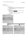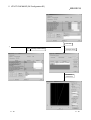
1
MITSUBISHI ELECTRIC
MELSEC System Q
Programmable Logic Controllers
User's Manual
Q64AD-GH, Q62AD-DGH
Channel Isolated High-Res.
Analog-Digital Converter Modules
Art. no.: 146547
01 08 2004
SH (NA)-080277
Version E
MITSUBISHI ELECTRIC
INDUSTRIAL AUTOMATION
• SAFETY PRECAUTIONS •
(Always read these instructions before using this equipment.)
Before using this product, please read this manual and the relevant manuals introduced in this manual
carefully and pay full attention to safety to handle the product correctly.
The instructions given in this manual are concerned with this product. For the safety instructions of the
PLC system, please read the user's manual for the CPU module to use.
In this manual, the safety instructions are ranked as "DANGER" and "CAUTION".
DANGER
Indicates that incorrect handling may cause hazardous conditions,
resulting in death or severe injury.
! CAUTION
Indicates that incorrect handling may cause hazardous conditions,
resulting in medium or slight personal injury or physical damage.
!
Note that the ! CAUTION level may lead to a serious consequence according to the circumstances.
Always follow the instructions of both levels because they are important to personal safety.
Please store this manual in a safe place and make it accessible when required. Always forward it to the
end user.
[DESIGN PRECAUTION]
!
DANGER
• Do not write data into the "system area" of the buffer memory of intelligent function modules.
Also, do not use any "prohibited to use" signals as an output signal to an intelligent function
module from the PLC CPU.
Writing data into the "system area" or outputting a signal for "prohibited to use" may cause a
PLC system malfunction.
!
CAUTION
• Do not bunch the control wires or communication cables with the main circuit or power wires, or
install them close to each other.
They should be installed 100mm(3.9inch) or more from each other.
Not doing so could result in noise that may cause malfunction.
A-1
A-1
[INSTALLATION PRECAUTIONS]
!
CAUTION
• Use the PLC in an environment that meets the general specifications contained in the user's
manual of the CPU module to use.
Using this PLC in an environment outside the range of the general specifications may cause
electric shock, fire, malfunction, and damage to or deterioration of the product.
• While pressing the installation lever located at the bottom of module, insert the module fixing tab
into the fixing hole in the base unit until it stops. Then, securely mount the module with the fixing
hole as a supporting point.
Improper installation may result in malfunction, breakdown or the module coming loose and
dropping.
Securely fix the module with screws if it is subject to vibration during use.
• Tighten the screws within the range of specified torque.
If the screws are loose, it may cause the module to fallout, short circuits, or malfunction.
If the screws are tightened too much, it may cause damage to the screw and/or the module,
resulting in fallout, short circuits or malfunction.
• Switch all phases of the external power supply off when mounting or removing the module.
Not doing so may cause damage to the module.
In the system where a CPU module supporting the online module change is used and on the
MELSECNET/H remote I/O stations, modules can be replaced online (during energizing).
However, there are some restrictions on replaceable modules and the replacement procedures
are predetermined for each module.
For details, refer to the chapter of the online module change in this manual.
• Do not directly touch the conductive area or electronic components of the module.
Doing so may cause malfunction or failure in the module.
[WIRING PRECAUTIONS]
!
CAUTION
• Always ground the FG terminal of the Q62AD-DGH.
Not doing so can cause an electric shock or malfunction.
• When turning on the power and operating the module after wiring is completed, always attach
the terminal cover that comes with the product.
There is a risk of electric shock if the terminal cover is not attached.
• Tighten the terminal screws within the range of specified torque.
If the terminal screws are loose, it may result in short circuits or malfunction.
If the terminal screws are tightened too much, it may cause damage to the screw and/or the
module, resulting in short circuits or malfunction.
• Be careful not to let foreign matter such as sawdust or wire chips get inside the module.
They may cause fires, failure or malfunction.
• The top surface of the module is covered with protective film to prevent foreign objects such as
cable offcuts from entering the module when wiring.
Do not remove this film until the wiring is complete.
Before operating the system, be sure to remove the film to provide adequate ventilation.
A-2
A-2
[STARTING AND MAINTENANCE PRECAUTIONS]
!
CAUTION
• Do not disassemble or modify the modules.
Doing so could cause failure, malfunction injury or fire.
• Switch all phases of the external power supply off when mounting or removing the module.
Not doing so may cause failure or malfunction of the module.
In the system where a CPU module supporting the online module change is used and on the
MELSECNET/H remote I/O stations, modules can be replaced online (during energizing).
However, there are some restrictions on replaceable modules and the replacement procedures
are predetermined for each module.
For details, refer to the chapter of the online module change in this manual.
• Do not mount/remove the module onto/from base unit more than 50 times (IEC 61131-2compliant), after the first use of the product.
Failure to do so may cause the module to malfunction due to poor contact of connector.
• Do not touch the connector while the power is on.
Doing so may cause malfunction.
• Switch all phases of the external power supply off when cleaning or retightening the terminal
screws and module installation screws.
Not doing so may cause failure or malfunction of the module.
If the screws are loose, it may cause the module to fallout, short circuits, or malfunction.
If the screws are tightened too much, it may cause damages to the screws and/or the module,
resulting in the module falling out, short circuits or malfunction.
• Always make sure to touch the grounded metal to discharge the electricity charged in the body,
etc., before touching the module.
Failure to do so may cause a failure or malfunctions of the module.
[DISPOSAL PRECAUTIONS]
!
CAUTION
• When disposing of this product, treat it as industrial waste.
A-3
A-3
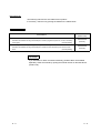
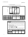
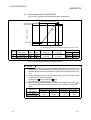
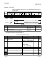
REVISIONS
The manual number is given on the bottom left of the back cover.
Print Date
May, 2002
Feb., 2003
May, 2003
Manual Number
Revision
SH (NA)-080277-A First edition
SH (NA)-080277-B Correction
Safety precautions, Section 2.1, 3.4.1, 3.4.23, 4.4.2, 5.1, 5.5.2, 5.6.1,
5.6.3, 6.3.2, 6.5.2, 7.3.4, 7.3.6, 7.4, Appendix 1.2, Appendix 1.3
SH (NA)-080277-C Addition
Section 2.3
Correction
Section 2.2, 3.4.1, 3.4.22, 3.4.23, 4.5, 4.6, 4.6.1, 4.6.2, 5.3.1
May, 2004
SH (NA)-080277-D
Correction
Section 2.2, 2.3, 3.1.1, 3.1.3, 3.2.1, 7.1, 7.3.1 to 7.3.6, 8.2.6
Aug., 2004
SH (NA)-080277-E
Addition
Section 5.6.3, 5.7, 5.8
Correction
Section 1.1, 5.1, 5.2.1, 5.2.2, 5.3.1, 5.3.2, 5.3.3, 5.6.1, 5.6.2,
Appendix 1.3
Japanese Manual Version SH-080262-F
This manual confers no industrial property rights or any rights of any other kind, nor does it confer any patent
licenses. Mitsubishi Electric Corporation cannot be held responsible for any problems involving industrial property
rights which may occur as a result of using the contents noted in this manual.
2002 MITSUBISHI ELECTRIC CORPORATION
A-4
A-4
INTRODUCTION
Thank you for purchasing the MELSEC-Q series PLC.
Before using the equipment, please read this manual carefully to develop full familiarity with the functions
and performance of the Q series PLC you have purchased, so as to ensure correct use.
Please forward a copy of this manual to the end user.
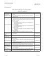
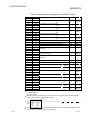
CONTENTS
SAFETY PRECAUTIONS..............................................................................................................................A- 1
REVISIONS ....................................................................................................................................................A- 4
INTRODUCTION............................................................................................................................................A- 5
CONTENTS....................................................................................................................................................A- 5
About Manuals ...............................................................................................................................................A- 9
Conformation to the EMC Directive and Low Voltage Instruction ................................................................A-10
About the Generic Terms and Abbreviations ................................................................................................A-11
Product Structure ...........................................................................................................................................A-12
1 OVERVIEW
1- 1 to 1- 3
1.1 Features .................................................................................................................................................. 1- 1
2 SYSTEM CONFIGURATION
2- 1 to 2- 4
2.1 Applicable Systems................................................................................................................................. 2- 1
2.2 How to Check the Function Version, Serial Number, Product Information and Software Version ...... 2- 3
2.3 Cautions for Power Supply from Q61P-A1/A2 to Q64AD-GH............................................................... 2- 4
3 SPECIFICATIONS
3- 1 to 3-49
3.1 Performance Specifications .................................................................................................................... 3- 1
3.1.1 Performance specifications list ........................................................................................................ 3- 1
3.1.2 I/O conversion characteristic............................................................................................................ 3- 4
3.1.3 Accuracy........................................................................................................................................... 3- 9
3.2 Function List ............................................................................................................................................ 3-10
3.2.1 A/D conversion methods.................................................................................................................. 3-11
3.2.2 Maximum and minimum values hold function ................................................................................. 3-13
3.2.3 Input signal error detection function ................................................................................................ 3-13
3.2.4 Warning output function ................................................................................................................... 3-14
3.2.5 A/D conversion starting time setting function (Q62AD-DGH only) ................................................. 3-18
3.3 I/O Signals for the PLC CPU .................................................................................................................. 3-19
3.3.1 List of I/O signals .............................................................................................................................. 3-19
3.3.2 Details of I/O signals ........................................................................................................................ 3-21
3.4 Buffer Memory......................................................................................................................................... 3-28
3.4.1 Buffer memory assignment.............................................................................................................. 3-28
3.4.2 A/D conversion enable/disable setting (buffer memory address 0: Un\G0)................................... 3-36
3.4.3 CH Average time/Average number of times/Move average/Time constant settings
(buffer memory addresses 1 to 4: Un\G1 to Un\G4)....................................................................... 3-37
3.4.4 CH A/D conversion starting time setting
(buffer memory addresses 5, 6: Un\G5, Un\G6) (Q62AD-DGH only) ............................................ 3-37
A-5
A-5
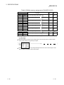
3.4.5 Averaging process specification (buffer memory address 9: Un\G9)............................................. 3-38
3.4.6 A/D conversion completed flag (buffer memory address 10: Un\G10) .......................................... 3-39
3.4.7 CH digital output value (16bit) (buffer memory addresses 11 to 14: Un\G11 to Un\G14).......... 3-39
3.4.8 Write data error codes (buffer memory address 19: Un\G19) ........................................................ 3-40
3.4.9 Setting range (buffer memory address 20: Un\G20)....................................................................... 3-40
3.4.10 Offset/gain setting mode (buffer memory addresses 22, 23: Un\G22, Un\G23) ......................... 3-41
3.4.11 CH maximum value/minimum value storage area (16bit)
(buffer memory addresses 30 to 37: Un\G30 to Un\G37) ............................................................ 3-41
3.4.12 Input signal error detection/warning output settings (buffer memory address 47: Un\G47)........ 3-42
3.4.13 Warning output flag (buffer memory address 48 :Un\G48) .......................................................... 3-42
3.4.14 Input signal error detection flag (buffer memory address 49: Un\G49)........................................ 3-43
3.4.15 CH digital output value (32bit) (buffer memory addresses 54 to 61: Un\G54 to Un\G61)........ 3-43
3.4.16 CH maximum value/minimum value storage area (32bit)
(buffer memory addresses 62 to 77: Un\G62 to Un\G77) ............................................................ 3-44
3.4.17 CH process alarm upper/lower limit value
(buffer memory addresses 86 to 117: Un\G86 to Un\G117) ........................................................ 3-44
3.4.18 CH rate alarm warning detection period
(buffer memory addresses 118 to 121: Un\G118 to Un\G121) .................................................... 3-45
3.4.19 CH rate alarm upper/lower limit value
(buffer memory addresses 122 to 137: Un\G122 to Un\G137) .................................................... 3-46
3.4.20 CH input signal error detection setting value
(buffer memory addresses 138 to 141: Un\G138 to Un\G141) .................................................... 3-47
3.4.21 Mode switching setting (buffer memory addresses 158, 159: Un\G158, Un\G159).................... 3-48
3.4.22 Pass data classification setting (buffer memory addresses 200: Un\G200) (Q64AD-GH only).. 3-48
3.4.23 Industrial shipment settings and user range settings offset/gain value
(buffer memory addresses 202 to 233: Un\G202 to Un\G233) .................................................... 3-49
4 SETUP AND PROCEDURES BEFORE OPERATION
4- 1 to 4-17
4.1 Handling Precautions.............................................................................................................................. 4- 1
4.2 Setup and Procedures before Operation ............................................................................................... 4- 2
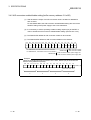
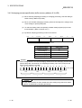
4.3 Part Identification Nomenclature ............................................................................................................ 4- 3
4.4 Wiring....................................................................................................................................................... 4- 5
4.4.1 Wiring precautions............................................................................................................................ 4- 5
4.4.2 External wiring .................................................................................................................................. 4- 6
4.5 Switch Setting for Intelligent Function Module ....................................................................................... 4- 8
4.6 Offset/Gain Settings ................................................................................................................................ 4-10
4.6.1 Offset/Gain Settings (Q64AD-GH)................................................................................................... 4-10
4.6.2 Offset/Gain Settings (Q62AD-DGH)................................................................................................ 4-14
4.6.3 A/D conversion value storage during offset/gain setting................................................................. 4-17
5 UTILITY PACKAGE (GX Configurator-AD)
5- 1 to 5-31
5.1 Utility Package Functions........................................................................................................................ 55.2 Installing and Uninstalling the Utility Package........................................................................................ 55.2.1 User precautions .............................................................................................................................. 55.2.2 Operating environment..................................................................................................................... 5-
A-6
A-6
1
2
2
4
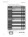
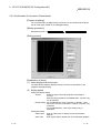
5.3 Explanation of Utility Package Operation............................................................................................... 5- 5
5.3.1 How to perform common utility package operations....................................................................... 5- 5
5.3.2 Operation overview .......................................................................................................................... 5- 8
5.3.3 Starting the intelligent function module utility .................................................................................. 5-10
5.4 Initial Setting............................................................................................................................................ 5-13
5.5 Automatic Refresh Setting ...................................................................................................................... 5-15
5.6 Monitor/Test ............................................................................................................................................ 5-17
5.6.1 Monitor/test screen........................................................................................................................... 5-17
5.6.2 Offset/gain setting operation ............................................................................................................ 5-20
5.6.3 Confirmation of Conversion Characteristic....................................................................................... 5-21
5.6.4 Pass data (Q64AD-GH) .................................................................................................................... 5-23
5.6.5 Pass data (Q62AD-DGH).................................................................................................................. 5-25
5.7 FB Conversion of Initial Setting/Auto Refresh Setting ............................................................................ 5-26
5.8 Usage of FB ............................................................................................................................................. 5-27
5.8.1 Outline................................................................................................................................................ 5-27
5.8.2 Paste an FB to a Sequence Program............................................................................................... 5-29
5.8.3 Convert (Compile) a Sequence Program ......................................................................................... 5-30
6 PROGRAMMING
6- 1 to 6-23
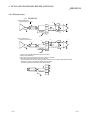
6.1 Programming Procedure......................................................................................................................... 6- 1
6.2 For Use in Normal System Configuration (Q64AD-GH) ........................................................................ 6- 2
6.2.1 Programming Example Using the Utility Package .......................................................................... 6- 3
6.2.2 Programming Example without Using the Utility Package.............................................................. 6- 5
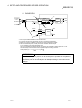
6.3 For Use in Remote I/O Network (Q64AD-GH)....................................................................................... 6- 7
6.3.1 Programming Example Using the Utility Package .......................................................................... 6- 8
6.3.2 Programming Example without Using the Utility Package.............................................................. 6-11
6.4 For Use in Normal System Configuration (Q62AD-DGH) ..................................................................... 6-14
6.4.1 Programming Example Using the Utility Package .......................................................................... 6-15
6.4.2 Programming Example without Using the Utility Package.............................................................. 6-17
6.5 For Use in Remote I/O Network (Q62AD-DGH) .................................................................................... 6-18
6.5.1 Programming Example Using the Utility Package .......................................................................... 6-19
6.5.2 Programming Example without Using the Utility Package.............................................................. 6-21
7 ONLINE MODULE CHANGE
7- 1 to 7-36
7.1 Online Module Change Conditions......................................................................................................... 7- 2
7.2 Online Module Change Operations ........................................................................................................ 7- 3
7.3 Online Module Change Procedure ......................................................................................................... 7- 4
7.3.1 When industrial shipment setting is used and initial setting was made with
GX Configurator-AD ......................................................................................................................... 7- 4
7.3.2 When industrial shipment setting is used and initial setting was made with sequence program.. 7- 9
7.3.3 When user range setting is used and initial setting was made with GX Configurator-AD
(other system is available) ............................................................................................................... 7-14
7.3.4 When user range setting is used and initial setting was made with GX Configurator-AD
(other system is unavailable) ........................................................................................................... 7-19
7.3.5 When user range setting is used and initial setting was made with sequence program
(other system is available) ............................................................................................................... 7-25
A-7
A-7
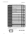
7.3.6 When user range setting is used and initial setting was made with sequence program
(other system is unavailable) ........................................................................................................... 7-30
7.4 Range Reference Table.......................................................................................................................... 7-35
7.5 Precautions for Online Module Change ................................................................................................. 7-36
8 TROUBLESHOOTING
8- 1 to 8- 6
8.1 Error Code List ........................................................................................................................................ 88.2 Troubleshooting ...................................................................................................................................... 88.2.1 When the "RUN" LED is flashing or turned off................................................................................ 88.2.2 When the "ERR." LED is on or flashing........................................................................................... 88.2.3 When the "ALM" LED is on or flashing............................................................................................ 88.2.4 When the digital output values cannot be read............................................................................... 88.2.5 When A/D conversion completed flag does not turn ON during use in normal mode ................... 88.2.6 Checking the A/D converter module status using GX Developer system monitor ........................ 8APPENDIX
1
3
3
3
3
4
5
5
App.- 1 to App.-14
Appendix 1 Dedicated Instruction List .....................................................................................................App.- 1
Appendix 1.1 OFFGAN ........................................................................................................................App.- 2
Appendix 1.2 OGLOAD........................................................................................................................App.- 4
Appendix 1.3 OGSTOR........................................................................................................................App.- 8
Appendix 2 Performance Comparison between Q64AD-GH and Q64AD.............................................App.-13
Appendix 3 External Dimensions.............................................................................................................App.-14
INDEX
A-8
Index- 1 to Index- 3
A-8
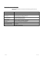
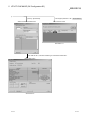
About Manuals
The following manuals are also related to this product.
If necessary, order them by quoting the details in the tables below.
Related Manuals
Manual Name
GX Developer Version 8 Operating Manual
Describes the methods of using GX Developer to create a program and print out, monitor, and debug
the program.
(Sold separately)
GX Developer Version 8 Operating Manual (Function Block)
Describes the methods of using GX Developer to create a function block and print out the function
block.
(Sold separately)
Manual Number
(Model Code)
SH-080373E
(13JU41)
SH-080376E
(13JU44)
REMARK
If you would like to obtain a manual individually, printed matters are available
separately. Order the manual by quoting the manual number on the table above
(model code).
A-9
A-9
Conformation to the EMC Directive and Low Voltage Instruction
For details on making Mitsubishi PLC conform to the EMC directive and low voltage
instruction when installing it in your product, please see Chapter 3, "EMC Directive
and Low Voltage Instruction" of the User's Manual (Hardware) of the PLC CPU to
use.
The CE logo is printed on the rating plate on the main body of the PLC that conforms
to the EMC directive and low voltage instruction.
By making this product conform to the EMC directive and low voltage instruction, it is
not necessary to make those steps individually.
A - 10
A - 10
About the Generic Terms and Abbreviations
Unless otherwise specified, this manual uses the following general terms and
abbreviations.
Abbreviation/general terms
Description of the abbreviation/general terms
A/D converter module
Generic term for Q64AD-GH and Q62AD-DGH
DOS/V personal computer
IBM PC/AT or compatible computer with DOS/V.
GX Developer
GX Configurator-AD
QCPU (Q mode)
®
Generic product name of the product types SWnD5C-GPPW-E, SWnD5C-GPPW-EA,
SWnD5C-GPPW-EV and SWnD5C-GPPW-EVA.
"n" in the model name is 4 or greater.
Generic term for analog-digital converter module setting and monitor tool GX
Configurator-AD (SW2D5C-QADU-E)
Generic term for Q00JCPU, Q00CPU, Q01CPU, Q02CPU, Q02HCPU, Q06HCPU,
Q12HCPU, Q25HCPU, Q12PHCPU, Q25PHCPU
QnPHCPU
Generic term for Q12PHCPU and Q25PHCPU.
Personal computer
Generic term for DOS/V personal computer
Industrial shipment setting
Generic term for analog input ranges 0 to 10V, 0 to 5V, 1 to 5V, -10 to 10V, 0 to 20mA
and 4 to 20mA
FB
Abbreviation of function block.
A - 11
A - 11
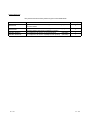
Product Structure
The product structure of this product is given in the table below.
Model code
Q64AD-GH
Q62AD-DGH
Product name
Quantity
Type Q64AD-GH Channel Isolated High Resolution Analog-Digital
Converter Module
Type Q62AD-DGH Channel Isolated High Resolution Analog-Digital
Converter Module (with Signal Conditioning Function)
1
1
SW2D5C-QADU-E
GX Configurator-AD Version 2 (1-license product)
(CD-ROM)
1
SW2D5C-QADU-EA
GX Configurator-AD Version 2 (Multiple-license product)
(CD-ROM)
1
A - 12
A - 12
1 OVERVIEW
MELSEC-Q
1 OVERVIEW
This User's Manual describes the specifications, handling and programming methods
for the type Q64AD-GH channel isolated high resolution analog-digital converter
module (hereinafter referred to as the Q64AD-GH) and type Q62AD-DGH channel
isolated high resolution analog-digital converter module (with signal conditioning
function) (hereinafter referred to as the Q62AD-DGH), which are used with the
MELSEC-Q series CPU modules.
The Q62AD-DGH is exclusively used for current input.
In this manual, the Q64AD-GH and Q62AD-DGH are collectively referred to as the A/D
converter modules.
1.1 Features
(1) Channel isolated
The channels are isolated.
The Q62AD-DGH is also isolated between the external supply power and
channels.
(2) High resolution
The resolution is as high as 32-bit signed binary (data part is 16 bits long). (When
the -10V to +10V range is selected)
(3) Power supply to 2-wire transmitter (Q62AD-DGH only)
Supplying power to the 2-wire transmitter, the Q62AD-DGH does not require the
power supply for the 2-wire transmitter.
Supply power can be switched ON/OFF channel-by-channel by the A/D
conversion enable/disable setting.
(4) Module protection provided by short-circuit protection circuit
(Q62AD-DGH only)
If an excessive current flows into the module due to a short circuit of the wiring,
the short-circuit protection circuit limits the current to within 25 to 35mA,
protecting the module.
(5) Analog input check by check terminals (Q62AD-DGH only)
Measurement of a voltage at the check terminals allows the mA of the 2-wire
transmitter output to be checked without the wiring being disconnected.
(6) High accuracy
1
The reference accuracy
is as high as ±0.05% and the temperature coefficient
is as high as ±71.4ppm/°C.
1 Accuracy of offset/gain setting at ambient temperature
2 Accuracy per temperature change of 1°C
Example) Accuracy when the temperature varies from 25°C to 30°C
0.05% (reference accuracy) + 0.00714%/°C (temperature
coefficient) 5°C (temperature variation difference) = 0.0857%
1-1
1-1
2
1
1 OVERVIEW
MELSEC-Q
(7) Changing the input range
The input range 3 can easily be set from the GX Developer.
3 Input range refers to the type of offset/gain settings. The most frequently
used range is set as the default but the user can also set the offset/gain.
1
(8) A/D conversion system
There are the following five A/D conversion systems.
(a) Sampling processing
Analog input values are converted into digital values one by one on a
channel basis and the digital output value is output at every conversion.
(b) Averaging processing
1) Time averaging
A/D conversion is averaged in terms of time on a channel basis and a
digital average value is output.
2) Count averaging
A/D conversion is averaged in terms of count on a channel basis and a
digital average value is output.
3) Move averaging
The specified number of digital output values measured per sampling
time are averaged.
(c) Primary delay filter
A digital output value is smoothed according to the preset time constant.
(9) Input signal error detection function
The voltage/current outside the setting range is detected.
(10) Warning output
There are the following two warning outputs.
(a) Process alarm
A warning is output if a digital output value falls outside the setting range.
(b) Rate alarm
A warning is output if the varying rate of a digital output value falls outside
the preset varying rate range.
(11) Online module change
The module can be changed without the system being stopped.
Further, the dedicated instruction (G. OGLOAD, G. OGSTOR), write to the buffer
memory, or turning ON the Y signal enables "inheritance of offset/gain settings to
the new A/D converter module replacing the old one changed online" and
"transfer of offset/gain settings to the other A/D converter module mounted on the
other slot". (These apply to the modules of the same model.)
1-2
1-2
1 OVERVIEW
MELSEC-Q
(12) Offset/gain setting
GX Configurator-AD, dedicated instruction (G. OFFGAN) or mode switching
setting allows a shift to the offset/gain setting mode easily.
(13) Easy settings using the utility package
A utility package is sold separately (GX Configurator-AD).
The utility package is not a required item, however, it is useful for on-screen
setting of the intelligent function module parameters (initial setting/auto refresh
setting). In addition, FB 1 can be generated automatically from the intelligent
function module parameters that have been set up and used in a sequence
program.
1: FB is the function for making a circuit block used in a sequence program
repeatedly a part (FB) to use it in the sequence program.
This function can improve the efficiency of program development and
minimize program bugs to improve program qualities.
For the details of FB, refer to "GX Developer Version 8 Operating Manual
(Function Block)."
1-3
1-3
2 SYSTEM CONFIGURATION
MELSEC-Q
2 SYSTEM CONFIGURATION
2.1 Applicable Systems
This section describes the system configuration for the A/D converter module.
2
(1) Applicable module and the number of modules that can be installed
The following are the CPU module and network module (for remote I/O stations)
in which the A/D converter module can be installed and the number of modules
that can be installed.
Applicable module
CPU module
Network module
Number of modules that
can be installed
Q00JCPU
Maximum 16
Q00CPU
Q01CPU
Maximum 24
Q02CPU
Q02HCPU
Q06HCPU
Q12HCPU
Q25HCPU
Maximum 64
Q12PHCPU
Q25PHCPU
Maximum 64
QJ72LP25-25
QJ72BR15
QJ72LP25G
Maximum 64
Remarks
( 1)
Can be installed in Q mode only
( 1)
( 1)
MELSECNET/H Remote I/O
station ( 2)
1 See User's Manual (Function Explanation, Program Fundamentals) for the CPU module to use.
2 See Q Corresponding MELSECNET/H Network System Reference Manual (Remote I/O
network).
(2) Base Unit in which the converter module can be installed
The A/D converter module can be installed in any I/O slot ( 3) of the base unit.
However, a power shortage may occur depending on the combination with other
installed modules and the number of modules used, so always take into
consideration the power supply capacity when installing modules.
3 Limited to the range of the number of I/O points in the CPU module and network module (for
remote I/O stations).
(3) Compatibility with a multiple PLC system
First read the QCPU (Q mode) user's manual (Function Explanation, Program
Fundamentals) if the A/D converter module is used with a multiple PLC system.
(a) Compatible A/D converter module
Use an A/D converter module with function version B or higher if using the
module in a multiple PLC system.
(b) Intelligent function module parameters
Perform PLC write of the intelligent function module parameters to the
control PLC of the A/D converter module only.
2-1
2-1
2 SYSTEM CONFIGURATION
MELSEC-Q
(4) Compatibility with online module change
To make an online module change, use the A/D converter module of function
version C or later.
POINT
The A/D converter module does not have the products of function versions A and B.
The products of function version C include the functions of the products of function
versions A and B.
2
(5) Q64AD-GH compatible software packages
The following table indicates the compatibility of the systems using the Q64ADGH with the software packages.
GX Developer is required when the Q64AD-GH is used.
Software Version
GX Developer
Single PLC system
Version 7 or later
Multiple PLC system
Version 8 or later
Q02/Q02H/Q06H/
Single PLC system
Version 4 or later
Q12H/Q25HCPU
Multiple PLC system
Version 6 or later
Q00J/Q00/Q01CPU
4
Version 1.14Q or later
Single PLC system
Q12PH/Q25PHCPU
GX Configurator-AD
Version 7.10L or later
Multiple PLC system
If installed in a MELSECNET/H remote I/O
station
Version 6 or later
4 When using the pass data, use the product of Version 1.16S or later.
(6) Q62AD-DGH compatible software packages
The following table indicates the compatibility of the systems using the Q62ADDGH with the software packages.
GX Developer is required when the Q62AD-DGH is used.
Software Version
GX Developer
Single PLC system
Version 7 or later
Multiple PLC system
Version 8 or later
Q02/Q02H/Q06H/
Single PLC system
Version 4 or later
Q12H/Q25HCPU
Multiple PLC system
Version 6 or later
Q00J/Q00/Q01CPU
Version 1.14Q or later
Single PLC system
Q12PH/Q25PHCPU
Multiple PLC system
If installed in a MELSECNET/H remote I/O
station
2-2
GX Configurator-AD
Version 7.10L or later
Version 6 or later
2-2
2 SYSTEM CONFIGURATION
MELSEC-Q
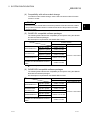
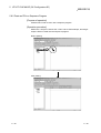
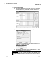
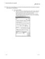
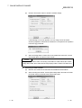
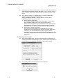
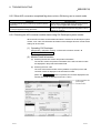
2.2 How to Check the Function Version, Serial Number, Product Information and Software
Version
This section describes how to check the function version, serial number, product
information of the A/D converter module and the software version of GX ConfiguratorAD.
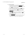
(1) How to check the function version, serial number and product
information of the A/D converter module
(a) To check the function version and serial number using the "SERIAL column
of the rating plate" located on the side of the module
Serial No. (First 6 digits)
Function version
Conformed standard
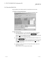
(b) To check the function version and product information using GX Developer
Refer to Section 8.2.6 of this manual.
(2) How to check the GX Configurator-AD software version
The GX Configurator-AD software version can be checked in GX Developer's
"Product information" screen.
[Startup procedure]
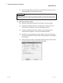
GX Developer
"Help"
Product information
Software version
(In the case of GX Developer Version 7)
2-3
2-3
2 SYSTEM CONFIGURATION
MELSEC-Q
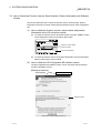
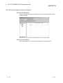
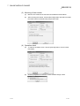
REMARK
The version indication for the GX Configurator-AD has been changed as shown
below from the SW0D5C-QADU-E 50F upgrade product.
Previous product
Upgrade and subsequent versions
GX Configurator-AD Version 1.10L
SW0D5C-QADU-E 50F
2.3 Cautions for Power Supply from Q61P-A1/A2 to Q64AD-GH
When using the Q61P-A1/A2 and Q64AD-GH in combination, it is required to use them
within the range in Table 2.1.
This requirement applies to the case where the Q64AD-GH satisfies any of the
following conditions.
The first six digits of serial number are "050914" or earlier.
The first five digits of "Product information" number are "05081" or earlier.
If it satisfies the above conditions but does not meet the ones outlined in Table 2.1,
carry out the following:
Replace the power supply module with the Q64P.
Mount the Q64AD-GH to another base unit.
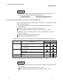
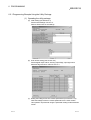
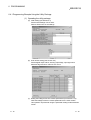
Table 2.1 Conditions for Use of Q61P-A1/A2 and Q64AD-GH in Combination
No. of Q64AD-GH
Conditions
modules
Available power supply
Q61P-A1/A2
Q64P
Total current consumption of all modules on the same
3 or less
base is 5.0A or less.
Total current consumption of all modules on the same
base exceeds 5.0A.
Module other than the Q64AD-GH is not mounted on
the same base.
4
Module other than the Q64AD-GH is mounted on the
same base.
5 or more
—
If the modules are used outside the condition range given in Table 2.1, the "POWER" LED of
the power supply module may flicker and the PLC CPU system may not start.
REMARK
When the Q64AD-GH satisfies any of the following conditions, the above precaution
does not apply.
The first six digits of serial number are "051217" or later.
The first five digits of "Product information" number are "05082" or later.
2-4
2-4
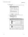
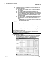
3 SPECIFICATIONS
MELSEC-Q
3 SPECIFICATIONS
The description of this chapter and later is based on the Q64AD-GH.
3.1 Performance Specifications
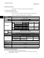
3.1.1 Performance specifications list
Table 3.1 shows the performance specifications of the A/D converter modules.
Table 3.1 Performance Specifications of Q64AD-GH
3
Model name
Item
Number of analog input
points
Voltage
Analog input
Current
Q64AD-GH
4 points (4 channels)
-10 to 10VDC (Input resistance 1 M )
0 to 20mADC (Input resistance 250 )
16-bit signed binary (-32768 to 32767)
32-bit signed binary (-65536 to 65535)
Digital output
Input
I/O characteristics,
maximum resolution
Accuracy
Reference
(Accuracy
accuracy 1
relative to
digital output Temperature
value)
coefficient 3
Common mode
characteristic
Conversion speed
Absolute maximum input
Analog input range
0 to 10V
0 to 5V
1 to 5V
Voltage
Users input range (Uni-polar)
-10 to 10V
Users input range (Bi-polar)
0 to 20mA
Current
4 to 20mA
Users input range (Uni-polar)
Maximum number of writes
for E2PROM
Number of I/O occupied
points
Connected terminal
Applicable wire size
Applicable solderless
terminals
Internal current
consumption (5VDC)
Weight
Digital output value Digital output value
(32-bit)
(16-bit)
0 to 64000
0 to 32000
-64000 to 64000
-32000 to 32000
0 to 64000
0 to 32000
±0.05%
Digital output value (32-bit) : ±32digit
Digital output value (16-bit) : ±16digit
2
2
±71.4ppm/°C (0.00714%/°C)
Common mode voltage Input-Common ground (input voltage 0V): 1780VAC
Common mode voltage rejection ratio (VCM < 1780V): 60Hz 105dB, 50Hz 107dB
10ms/4 channels
Voltage: ± 15V Current: ± 30mA
Specific isolated area
Isolation specifications
Maximum resolution
32-bit
16-bit
156.3µV
312.6µV
78.2µV
156.4µV
62.5µV
125.0µV
47.4µV
94.8µV
156.3µV
312.6µV
47.4µV
94.8µV
312.5nA
625.0nA
250.0nA
500.0nA
151.6nA
303.2nA
Between I/O terminal and
PLC power supply
Between analog input
channels
Isolation method
Photocoupler isolation
Transformer isolation
Dielectric withstand
voltage
1780VAC rms/3 cycles
(elevation 2000m)
500VDC 10M
more
or
100,000
16 points
18 points terminal block
0.3 to 0.75mm2
R1.25-3 (Solderless terminals with sleeves are not applicable)
0.89A
0.20kg
1: Accuracy of offset/gain setting at ambient temperature
2: "digit" indicates a digital output value.
3: Accuracy per temperature change of 1°C
Example) Accuracy when temperature changes from 25 to 30°C
0.05% (reference accuracy) + 0.00714 %/°C (temperature coefficient)
change difference) = 0.0857%
3-1
Insulation resistance
5°C (temperature
3-1
3 SPECIFICATIONS
MELSEC-Q
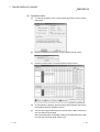
Table 3.2 Performance Specifications of Q62AD-DGH
Model name
Q62AD-DGH
Item
Number of
analog input
Input
specification points
Analog input
Connecting
Supply voltage
with 2-wire
Supply
Maximum
transmitter
power
supply current
specification Short-circuit
protection
Check terminals
2 points (2 channels)
4 to 20mADC
24mADC
Available
Limit current: 25 to 35mA
Available
16-bit signed binary (-768 to 32767)
32-bit signed binary (-1536 to 65535)
Digital output
I/O characteristics, Maximum resolution
Analog input range
Maximum resolution
32-bit
16-bit
4 to 20mA
Users range setting
250.0nA
151.6nA
Accuracy
Reference accuracy 1
(Accuracy
relative to
digital output
Temperature coefficient 3
value)
Conversion speed
Isolation specifications
Maximum number of writes for
E2PROM
Number of I/O occupied points
Connected terminal
Applicable wire size
Applicable solderless terminals
External supply power
Internal current consumption (5VDC)
Weight
4(Input resistance 250 )
26±2VDC
3
Digital output value Digital output value
(32-bit)
(16-bit)
500.0nA
303.2nA
0 to 64000
±0.05%
Digital output value (32-bit): ±32digit
Digital output value (16-bit): ±16digit
0 to 32000
2
2
±71.4ppm/°C (0.00714 %/°C)
10ms/2 channels
Specific isolated area
Isolation method
Between I/O terminal and
PLC power supply
Between analog input
channels
Between external supply
power and analog input
Photocoupler
isolation
Transformer
isolation
Transformer
isolation
Dielectric withstand
voltage
Insulation
resistance
1780VAC rms/3 cycles
500VDC
(elevation 2000m)
10M or more
100,000
16 points
18 points terminal block
0.3 to 0.75mm2
R1.25-3 (Solderless terminals with sleeves are not applicable)
24VDC +20%, -15%
Ripple, spike within 500mVP-P
Inrush current : 5.5A, within 200µs
0.36A
0.22A
0.19kg
1: Accuracy of offset/gain setting at ambient temperature
Q62AD-DGH needs to be powered on 30 minutes prior to operation for compliance to the specification
(accuracy).
2: "digit" indicates a digital output value.
3: Accuracy per temperature change of 1°C
Example) Accuracy when temperature changes from 25 to 30°C
0.05% (reference accuracy) + 0.00714 %/°C (temperature coefficient) 5°C (temperature
change difference) = 0.0857%
4: User range setting is 2 to 24mA.
3-2
3-2
3 SPECIFICATIONS
MELSEC-Q
REMARK
See the user’s manual for the CPU module being used for general specifications of
the A/D converter modules.
3-3
3-3
3 SPECIFICATIONS
MELSEC-Q
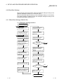
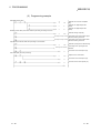
3.1.2 I/O conversion characteristic
The I/O conversion characteristic represents the angle formed by a straight line
connecting the "offset value" and "gain value" when the analog signals (voltage or
current input) from outside the PLC are converted to digital values.
Offset value
The offset value denotes the analog input value (voltage or current) that makes the
digital output value 0.
Gain value
The gain value denotes the analog input value (voltage or current) that makes the
digital output value:
32000 (16 bits)
64000 (32 bits)
3-4
3-4
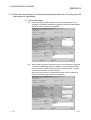
3 SPECIFICATIONS
MELSEC-Q
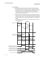
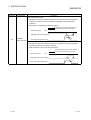
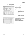
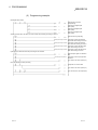
(1) Input characteristics of Q64AD-GH
(a) Voltage input characteristic
Fig. 3.1 shows a graph of the voltage input characteristic.
Analog input practical range
65535(32767)
64000(32000)
Digital output value
3)4)
2)
1)
0
-1536(-768)
1
-64000(-32000)
-65536(-32768)
-15
-10
0
5
-5
Analog input voltage (V)
10
15
The value within parentheses indicates the digital output value (16 bits).
Analog input
Offset
Gain
range setting
value
value
1)
1 to 5V
1V
5V
2)
0 to 5V
0V
5V
3)
-10 to 10V
0V
10V
4)
0 to 10V
0V
10V
1
1
1
1
Number
—
—
User range setting
(Uni-polar)
User range setting
(Bi-polar)
Digital output value Digital output value
(32 bits) 2
(16 bits) 2
0 to 64000
0 to 32000
-64000 to 64000
-32000 to 32000
0 to 64000
0 to 32000
-64000 to 64000
-32000 to 32000
Maximum resolution
32 bits
16 bits
62.5µV
125.0µV
78.2µV
156.4µV
156.3µV
312.6µV
47.4µV
94.8µV
Fig. 3.1 Voltage input characteristic of Q64AD-GH
3-5
3-5
3 SPECIFICATIONS
MELSEC-Q
POINT
(1) Set within the analog input range and digital output range for each input range.
If these ranges are exceeded, the maximum resolution and accuracy may not
fall within the performance specifications. (Avoid use in the dotted area of Fig.
3.1.)
(2) Do not input an analog input voltage of more than ± 15 V. The input elements
may be damaged.
(3) Set the offset/gain values for the user setting range 1 within a range in which
the following conditions are satisfied.
(a) Offset value, gain value setting range: -10V to 10V
(b) { (gain value) - (offset value) } > 3.030V
(4) When an analog value that exceeds the range for the digital output value 2 is
entered, the digital output value will be fixed at the maximum or minimum value.
Analog input
Digital output value (32 bits)
range setting
Minimum
1 to 5V
0 to 5V
-10 to 10V
Minimum
-1536
-768
-65536
-32768
0 to 10V
User range setting
Maximum
Digital output value (16 bits)
-1536
65535
-768
Maximum
32767
(Uni-polar)
User range setting
(Bi-polar)
3-6
-65536
-32768
3-6
3 SPECIFICATIONS
MELSEC-Q
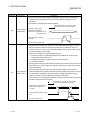
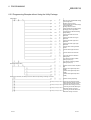
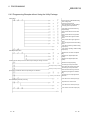
(b) Current input characteristic
Fig. 3.2 shows a graph of the current input characteristic.
Analog input practical range
Digital output value
65535(32767)
64000(32000)
1)
2)
0
-1536(-768)
4
-10
0
10
20
30
Analog input voltage (mA)
The value within parentheses indicates the digital output value (16 bits).
Number
Analog input
range setting
Offset
value
Gain
value
1)
4 to 20mA
4mA
20mA
2)
0 to 20mA
0mA
20mA
—
User range setting
(Uni-polar)
1
Digital output value Digital output value
(16 bits) 2
(32 bits) 2
0 to 64000
0 to 32000
1
Maximum resolution
32 bits
16 bits
250.0nA
500.0nA
312.5nA
625.0nA
151.6nA
303.2nA
Fig. 3.2 Current input characteristic of Q64AD-GH
POINT
(1) Set within the analog input range and digital output range for each input range.
If these ranges are exceeded, the maximum resolution and accuracy may not
fall within the performance specifications. (Avoid use in the dotted area of Fig.
3.2.)
(2) Do not input an analog input current of more than ± 30 mA. A breakdown may
result due to overheating.
(3) Set the offset/gain values for the user setting range 1 within a range in which
the following conditions are satisfied.
(a) Gain value 20mA, offset value 0mA
(b) { (gain value) - (offset value) } > 9.70mA
(4) When an analog value that exceeds the range of the digital output value 2 is
entered, the digital output value will be fixed at the maximum or minimum
value.
Analog input
range setting
Digital output value (32 bits)
Digital output value (16 bits)
Minimum
Maximum
Minimum
Maximum
-1536
65535
-768
32767
4 to 20mA
0 to 20mA
User range setting
(Uni-polar)
3-7
3-7
3 SPECIFICATIONS
MELSEC-Q
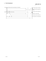
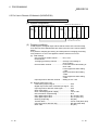
(2) Input characteristic of Q62AD-DGH
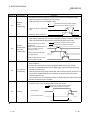
Fig. 3.3 shows a graph of the Q62AD-DGH input characteristic.
Analog input practical range
65535(32767)
64000(32000)
Digital output value
1)
0
-1536(-768)
4
-10
0
Analog input
range setting
Offset
value
Gain
value
1)
4 to 20mA
4mA
20mA
—
User range setting
Number
1
1
10
20 24
30
Analog input current (mA)
The value within parentheses indicates the digital output value (16 bits).
Digital output value Digital output value
(16 bits) 2
(32 bits) 2
0 to 64000
0 to 32000
Maximum resolution
32 bits
16 bits
250.0nA
500.0nA
151.6nA
303.2nA
Fig. 3.3 Input characteristic of Q62AD-DGH
POINT
(1) Set within the analog input range and digital output range for each input range.
If these ranges are exceeded, the maximum resolution and accuracy may not
fall within the performance specifications. (Avoid use in the dotted area of Fig.
3.3.)
(2) Set the offset/gain values for the user setting range 1 within a range in which
the following conditions are satisfied.
(a) Gain value 24mA, offset value 2mA
(b) { (gain value) - (offset value) } > 9.70mA
(3) When an analog value that exceeds the range of the digital output value 2 is
entered, the digital output value will be fixed at the maximum or minimum
value.
Analog input
range setting
4 to 20mA
User range setting
3-8
Digital output value (32 bits)
Digital output value (16 bits)
Minimum
Maximum
Minimum
Maximum
-1536
65535
-768
32767
3-8
3 SPECIFICATIONS
MELSEC-Q
3.1.3 Accuracy
The reference accuracy is the accuracy at the ambient temperature for offset/gain
setting.
The temperature coefficient is the accuracy per temperature variation of 1°C.
The reference accuracy is the accuracy relative to the maximum value of the digital
output value.
If you change the offset/gain setting or input range to change the input characteristic,
the reference accuracy and temperature coefficient do not vary and kept within the
ranges given in the performance specifications.
Example) Accuracy when the temperature varies from 25°C to 30°C
0.05% (reference accuracy) + 0.00714%/°C (temperature coefficient)
(temperature variation difference) = 0.0857%
3-9
5°C
3-9
3 SPECIFICATIONS
MELSEC-Q
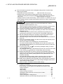
3.2 Function List
Table 3.3 lists the functions of the A/D converter modules.
Table 3.3 Function list
Item
Function
Reference section
(1) Specifies whether to enable or disable the A/D conversion for each
A/D conversion
enable/disable setting
channel.
(2) The conversion speed is 10ms regardless of the number of conversion
Section 3.4.2
enabled channels.
(1) Sampling processing
The A/D conversion for analog input values is performed successively for
each channel, and the digital output value is output upon each conversion.
(2) Averaging processing
(a) Time averaging
A/D conversion is averaged in terms of time on a channel basis and a
digital average value is output.
A/D conversion method
(b) Count averaging
Section 3.2.1
A/D conversion is averaged in terms of count on a channel basis and a
digital average value is output.
(c) Move averaging
The specified number of digital output values measured per sampling time
are averaged.
(3) Primary delay filter
A digital output value is smoothed according to the preset time constant.
Maximum and
minimum values hold
(1) The maximum and minimum values of the digital output values is retained
in the module.
Section 3.2.2
function
Input signal error
(1) The voltage/current outside the setting range is detected.
detection function
Section 3.2.3
(1) Process alarm
A warning is output if a digital output value falls outside the setting range.
Warning output function (2) Rate alarm
Section 3.2.4
A warning is output if the varying rate of a digital output value falls outside
the preset varying rate range.
A/D conversion starting (1) Setting the A/D conversion starting time allows A/D conversion to be
time setting function
started at the point when the output of the 2-wire transmitter stabilizes.
Section 3.2.5
(Q62AD-DGH only)
Supply power ON/OFF
function
(Q62AD-DGH only)
(1) The power supply to the 2-wire transmitter can be switched ON/OFF
channel by channel.
(2) Power is supplied to the channel set for "Conversion enable" in the A/D
conversion enable/disable setting (buffer memory address 0: Un\G0).
Online module change (1) The module can be changed without the system being stopped.
3 - 10
Section 3.4.2
Chapter 7
3 - 10
3 SPECIFICATIONS
MELSEC-Q
3.2.1 A/D conversion methods
(1) Sampling processing
A/D conversion is performed successively for the analog input value, and the
converted digital output values are stored in the buffer memory.
The conversion speed is 10ms regardless of the number of conversion enabled
channels.
(2) Averaging processing
(a) Time averaging
A/D conversion is made for the preset period of time, the sum of values other
than the maximum and minimum values is averaged, and the result is stored
into the buffer memory.
The processing count within the set time is uniform independently of the
number of used channels (number of channels set for A/D conversion enable).
Processing count = set time/10 (times)
[Example] When the averaging processing time is set to 42ms
42/10 = 4.2 (times) ... Fractional portion is dropped.
(b) Count averaging
A/D conversion is made the preset number of times, the sum of values other
than the maximum and minimum values is averaged, and the result is stored
into the buffer memory.
The time when the count-based average value is stored into the buffer
memory is uniform independently of the number of used channels (number
of channels set for A/D conversion enable).
Processing time = set count
10 (ms)
[Example] When the averaging processing count is set to 5 times
5 10 = 50 (ms)
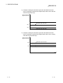
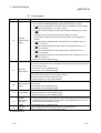
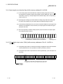
(c) Move averaging
The specified count of digital output values imported per sampling time are
averaged to find a value, which is then stored into the buffer memory.
Since average processing is performed with data shifted per sampling, the
most recent digital output value is available.
Move averaging processing at the preset count of 4 times
A/D conversion
value
64000
Sampling time
3)
2)
4)
5)
6)
1)
7)
8)
9)
12)
10) 11)
Buffer memory
32000
First storage
Second storage
Third storage
0
A/D conversion completed flag ON
Digital output
value
Time [ms]
Data transition inside buffer memory
3 - 11
First storage
Second storage
Third storage
1)+2)+3)+4)
2)+3)+4)+5)
3)+4)+5)+6)
4
4
4
3 - 11
3 SPECIFICATIONS
MELSEC-Q
(3) Primary delay filter
A digital value whose transient noise has been smoothed is output according to
the preset time constant.
The degree of smoothing varies with the time constant setting.
The relational expression of the time constant and digital output value is indicated
below.
[If n = 1]
Yn = 0
[If n = 2]
t
(yn - yn-1)
Yn = yn-1 +
t + TA
[If n 3]
t
(yn - Yn-1)
Yn = Yn-1 +
t + TA
Yn: Current digital output value
yn: Pre-smoothing digital output value
Yn-1: Immediately preceding
Yn-1: Immediately preceding digital
output value
pre-smoothing digital output value
n: Sampling count
t: A/D conversion time (0.01s)
TA: Time constant (s)
The A/D conversion completed flag turns ON when n 2.
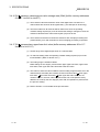
[Example 1] Digital output value when the analog input value varied from 0 to 1V
The variation of the digital output value at the time constant setting
of 1000ms (1s) is as shown below.
1000ms (1s) after the analog input value has reached 1V, the digital
output value reaches 63.2% of the value attained when the sampling
processing is selected.
Digital output value
12000
1
10000
0.8
8000
0.6
6000
0.4
4000
0.2
2000
0
0
1000
Digital output value
Analog input value (V)
Analog input value
1.2
0
Elapsed time (ms)
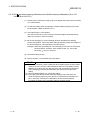
[Example 2] Digital output value when the variation of the analog input value has
a ringing waveform
The variations of the digital output values at the time constant setting
of 2000ms (2s), at the time constant setting of 1000ms (1s), and at
the move averaging processing of 16 times are as shown below.
Analog input value
Digital output value
(time constant setting: 1000ms)
Digital output value
(move averaging processing: 16 times)
Digital output value
(time constant setting: 2000ms)
12000
1
0.8
8000
0.6
6000
0.4
4000
0.2
2000
0
0
3 - 12
10000
0
Elapsed time (ms)
3 - 12
Digital output value
Analog input value (V)
1.2
3 SPECIFICATIONS
MELSEC-Q
3.2.2 Maximum and minimum values hold function
(1) The maximum and minimum values are held in the buffer memory channel by
channel.
(2) The maximum and minimum values are cleared to 0 when the maximum
value/minimum value reset request (YD) or operating condition setting request
(Y9) is turned ON, and new maximum and minimum values are stored when
conversion is started.
(3) Since the area for storing the maximum and minimum values can be rewritten with
the sequence program, the maximum and minimum values within a specific period
of time can be checked.
3.2.3 Input signal error detection function
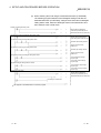
(1) If the input voltage/current rose to or above the input signal error detection upper
limit value or fell to or below the lower limit value, the input signal error detection
flag (buffer memory address 49: Un\G49) and input signal error detection signal
(XC) turn ON and the ALM LED flickers to indicate the error.
(2) The digital output value of the channel where the input signal error detection flag
(buffer memory address 49: Un\G49) turned ON is held as immediately before
detection of the error, and the A/D conversion completed flag (buffer memory
address 10: Un\G10) of the corresponding channel turns OFF.
(3) By bringing the analog input value within the setting range and then turning ON
the error clear request (YF), the input signal error detection flag (buffer memory
address 49: Un\G49) and input signal error detection signal (XC) turn OFF.
(4) When the analog input value returns to within the setting range, A/D conversion is
resumed independently of whether the input signal error detection flag (buffer
memory address 49: Un\G49) and input signal error detection signal (XC) are
reset or not, the A/D conversion completed flag (buffer memory address 10:
Un\G10) of the corresponding channel turns ON again after the first updating.
(The ERR. LED remains flickering.)
Analog input value
Error detection
Upper limit
value
CH1 analog
input value
Input value
normal
Lower limit
value
Time
CH1 input signal error detection flag
(Buffer memory address 49, b0)
Input signal error detection signal (XC)
CH1 A/D conversion completed flag
(Buffer memory address 10, b0)
Error clear request (YF)
3 - 13
3 - 13
3 SPECIFICATIONS
MELSEC-Q
(5) This function is executed at every sampling processing.
(6) Perform the following procedure to use this function.
1) Set the input signal error detection setting value for the corresponding channel.
2) Enable the A/D conversion of the corresponding channel.
3) Enable the input signal error detection of the corresponding channel.
4) Turn ON the operating condition setting request (Y9).
3.2.4 Warning output function
(1) Process alarm
(a) If the detected digital output value rose to or above the process alarm upper
upper limit value or fell to or below the process alarm lower lower limit value
and entered the warning output range zone, the warning output flag (buffer
memory address 48: Un\G48) and warning output signal (X8) turn ON and
the ALM LED is lit to indicate the warning.
(b) If, after the output of the warning, the detected digital output value fell below
the process alarm upper lower limit value or rose above the process alarm
lower upper limit value and returned to within the setting range, "0" is stored
into the bit position corresponding to the channel number of the warning
output flag (buffer memory address 48: Un\G48).
The warning output signal (X8) turns OFF only when all channels return to
within the setting range.
Digital output value
Upper upper
limit value
Warning
occurrence
Upper lower
limit value
Warning output range zone
Warning output range outside zone
Included
Warning
occurrence
Warning cancel
Warning cancel
CH1 digital output
value
Lower upper
limit value CH2 digital
Warning cancel
output value
Lower lower
limit value
Warning
occurrence
Time
CH1 process alarm upper limit value
(Buffer memory address 48, b0)
CH1 process alarm lower limit value
(Buffer memory address 48, b1)
CH2 process alarm upper limit value
(Buffer memory address 48, b2)
Warning output signal (X8)
(c) When time or count averaging is specified, this function is executed at
intervals of the preset averaging time or averaging count.
When any other A/D conversion system (sampling processing, move
averaging, primary delay filter) is specified, this function is executed at
intervals of the sampling time.
3 - 14
3 - 14
3 SPECIFICATIONS
MELSEC-Q
(2) Rate alarm
(a) If the digital output value sampled at intervals of the rate alarm warning
detection period indicated a varying rate equal to or greater than the rate
alarm upper limit value or a varying rate equal to or less than the rate alarm
lower limit value, the warning output flag (buffer memory address 48:
Un\G48) and warning output signal (X8) turn ON and the ALM LED is lit to
indicate the warning of the rate alarm.
(b) If, after the output of the warning, the varying rate fell below the rate alarm
upper limit value or rose above the rate alarm lower limit value and returned
to within the setting range, "0" is stored into the bit position corresponding to
the channel number of the warning output flag (buffer memory address 48:
Un\G48).
The warning output signal (X8) turns OFF only when all channels return to
within the setting range.
CH1 digital
output value
Rate alarm
warning detection
period
Digital output value
CH2 digital
output value
Varying rate (%) of
digital output value
Rate alarm
warning detection
period
Varying rate of
CH2 digital
output value
Time
Rate alarm
upper limit
value
Rate alarm
lower limit
value
Varying rate of
CH1 digital
output value
Time
CH1 rate alarm upper limit value
(Buffer memory address 48, b8)
CH1 rate alarm lower limit value
(Buffer memory address 48, b9)
CH2 rate alarm lower limit value
(Buffer memory address 48, b11)
Warning output signal (X8)
3 - 15
3 - 15
3 SPECIFICATIONS
MELSEC-Q
(c) Set the rate alarm upper limit value/lower limit value in 0.1%/s increments
relative to the maximum value (64000) of the digital output value.
The setting range is -65536 to 65535 (-6553.6% to 6553.5%).
(d) The setting range of the rate alarm warning detection period is 10 to
5000ms.
When the period is set to 5000ms, the digital values are compared at
intervals of 5 seconds to detect the varying rate.
(e) The rate alarm is judged by converting the rate alarm upper/lower limit value
into the digit value per rate alarm warning detection period.
The conversion expression of the value used to make judgment per rate
alarm warning detection period is as follows.
Value used to make judgment per rate alarm warning detection period [digit]
=rate alarm upper limit value or lower limit value 0.001 64000 rate
alarm warning detection period ÷ 1000
Example
When the varying rate upper limit value of channel 1 is set to 30%/s (300 is
stored into the buffer memory) and the rate alarm warning detection period of
channel 1 is 10ms, the current and previous values are compared at intervals of
10ms and whether or not the value has varied 0.3% (192 digits) or more in 10ms
is judged.
300 0.001 64000 10÷1000=192(digit)
(f) The rate alarm is useful to watch the varying rate of the digital output value in
the limited range.
1) Example of setting the rate alarm upper limit value/lower limit value
when it is desired to watch that the digital output value is at the rise rate
within the specified range
Varying rate (%) of
digital output value
Rate alarm upper limit value
+30%
+20%
Rate alarm lower limit value
0
Time
3 - 16
3 - 16
3 SPECIFICATIONS
MELSEC-Q
2) Example of setting the rate alarm upper limit value/lower limit value
when it is desired to watch that the digital output value is at the fall rate
within the specified range
Varying rate (%) of
digital output value
0
Rate alarm upper limit value
-20%
-30%
Rate alarm lower limit value
Time
3) Example of setting the rate alarm upper limit value/lower limit value
when it is desired to watch that the digital output value is at the varying
rate within the specified range
Varying rate (%) of
digital output value
Rate alarm upper limit value
+10%
0
-10%
Rate alarm lower limit value
Time
3 - 17
3 - 17
3 SPECIFICATIONS
MELSEC-Q
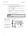
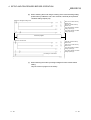
3.2.5 A/D conversion starting time setting function (Q62AD-DGH only)
(1) As the A/D conversion starting time, set the "time necessary from when the used
2-wire transmitter powers on until its output stabilizes".
This setting allows A/D conversion processing to be started as soon as the output
of the 2-wire transmitter stabilizes.
(2) Set the time to the CH A/D conversion starting time setting (buffer memory
addresses 5, 6: Un\G5, Un\G6).
(3) The following indicates the time until the A/D conversion completed flag (buffer
memory addresses 10: Un\G10) turns ON when the A/D conversion starting time
has been set.
(A/D conversion starting time) + (A/D conversion pre-processing: Approx. 150 to
165ms) + (A/D conversion processing: 10ms)
POINT
Set the A/D conversion starting time in consideration of the time necessary from
when the 2-wire transmitter powers on until its output stabilizes and the warm-up
time of the 2-wire transmitter.
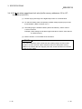
[Example] When the time necessary from when the 2-wire transmitter powers on until its output stabilizes is 500ms
A/D conversion enable/disable setting
(Power supply to 2-wire transmitter
ON/OFF)
(Buffer memory address 0: Un\G0)
A/D conversion enable
Power ON
When A/D conversion starting time is 0ms,
A/D conversion processing starts at this point.
26V power supply to 2-wire transmitter
Max.
20ms
When A/D conversion starting time is 500ms,
A/D conversion processing starts at this point.
500ms
Approx.150 to 165ms ON
Analog output of 2-wire transmitter
A/D conversion completed flag when A/D
conversion starting time is set to 500ms
(Buffer memory address 10: Un\G10)
A/D conversion completed flag when A/D
conversion starting time is set to 0ms
(Buffer memory address 10: Un\G10)
3 - 18
(A/D conversion
starting time)
Approx.
150 to 165ms
(A/D conversion
pre-processing)
(A/D conversion
pre-processing)
10ms
(A/D conversion
processing time)
ON
10ms (A/D conversion processing time)
3 - 18
3 SPECIFICATIONS
MELSEC-Q
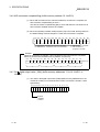
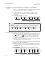
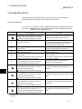
3.3 I/O Signals for the PLC CPU
3.3.1 List of I/O signals
Table 3.4 lists the I/O signals of the Q64AD-GH.
Table 3.5 lists the I/O signals of the Q62AD-DGH.
Note that I/O numbers (X/Y) shown in this chapter and thereafter are the values when
the start I/O number for the A/D converter module is set to 0.
Table 3.4 List of I/O signal (Q64AD-GH)
Signal direction CPU Module
Device No. (Input)
X0
Q64AD-GH
Signal name
Signal direction CPU Module
Device No. (Output)
Module ready
Q64AD-GH
Signal name
Y0
X1
Y1
X2
Y2
X3
Y3
Use prohibited
X4
1
Y4
X5
Y5
X6
Y6
X7
Y7
Use prohibited
1
X8
Warning output signal
Y8
X9
Operating condition setting completed flag
Y9
Operating condition setting request
XA
Offset/gain setting mode flag
YA
User range writing request
XB
Channel change completed flag
YB
XC
Input signal error detection signal
YC
Channel change request
Use prohibited 1
XD
Maximum value/minimum value reset
completed flag
YD
Maximum value/minimum value reset
XE
A/D conversion completed flag
YE
request
Use prohibited
XF
Error flag
YF
Error clear request
1
POINT
1 These signals cannot be used by the user since they are for system use only.
If these are turned ON/OFF by the sequence program, the functioning of the
A/D converter module cannot be guaranteed.
3 - 19
3 - 19
3 SPECIFICATIONS
MELSEC-Q
Table 3.5 List of I/O signal (Q62AD-DGH)
Signal direction CPU Module
Device No. (Input)
X0
Q62AD-DGH
Signal name
Signal direction CPU Module
Device No. (Output)
Module ready
Q62AD-DGH
Signal name
Y0
X1
Y1
X2
Y2
X3
Y3
Use prohibited
X4
1
Y4
X5
Y5
X6
Y6
X7
Y7
X8
Warning output signal
Use prohibited
1
Y8
X9
Operating condition setting completed flag
Y9
Operating condition setting request
XA
Offset/gain setting mode flag
YA
User range writing request
XB
Channel change completed flag
YB
Channel change request
YC
Offset/gain change request
XC
XD
Input signal error detection signal
Offset/gain change completed flag
Maximum value/minimum value reset
completed flag
YD
Maximum value/minimum value reset
XE
A/D conversion completed flag
YE
request
Use prohibited
XF
Error flag
YF
Error clear request
1
POINT
1 These signals cannot be used by the user since they are for system use only.
If these are turned ON/OFF by the sequence program, the functioning of the
A/D converter module cannot be guaranteed.
3 - 20
3 - 20
3 SPECIFICATIONS
MELSEC-Q
3.3.2 Details of I/O signals
I/O signals for the A/D converter modules are explained in detail below.
(1) Input signals
Device No.
Signal Name
Description
(1) When the PLC CPU is powered on or reset, this signal turns on once the preparation for
A/D conversion has been completed, and A/D conversion processing is then performed.
X0
Module ready
(2) In either of the following states, the Module ready (X0) turns OFF.
• During offset/gain setting mode (A/D conversion processing is performed.)
• When the A/D converter module has a watchdog timer error 1 (A/D conversion
processing is not performed.)
(1) The Warning output signal (X8) turns ON at detection of a process alarm or rate alarm.
(a) Process alarm
1) This signal turns ON when the digital output value falls outside the setting range
set to the process alarm upper/lower limit values (buffer memory addresses 86
to 117: Un\G86 to Un\G117) on any of the channels enabled for A/D conversion
after the process alarm function has been made valid.
2) As soon as the digital output values return to within the setting ranges on all
channels enabled for A/D conversion, this signal turns OFF automatically and
the ALM LED is also extinguished.
(b) Rate alarm
1) This signal turns ON when the varying rate of the digital output value falls
X8
Warning output
signal
outside the varying rate range set to the rate alarm upper/lower limit values
(buffer memory addresses 122 to 137: Un\G122 to Un\G137) on any of the
channels enabled for A/D conversion after the rate alarm function has been
made valid.
2) As soon as the varying rates of the digital output values return to within the
preset varying ranges on all channels enabled for A/D conversion, this signal
turns OFF automatically and the ALM LED is also extinguished.
Performed by the A/D converter module
Performed by the sequence program
Warning output flag
(Buffer memory address 48: Un\G48)
0
Warning occurrence
(Process alarm, rate alarm)
0
Warning output signal (X8)
1 A watchdog timer error occurs when the program calculations are not completed within the
scheduled time due to malfunctions of A/D converter module hardware.
When a watchdog timer error occurs, the RUN LED for the A/D converter module turns off.
3 - 21
3 - 21
3 SPECIFICATIONS
Device No.
MELSEC-Q
Signal Name
Description
(1) This signal is used as an interlock condition to turn ON/OFF the Operating condition
setting request (Y9) when any of the following settings has been changed.
• A/D conversion enable/disable setting (buffer memory address 0: Un\G0)
• CH
Average time/Average number of times/Move average/Time constant settings
(buffer memory addresses 1 to 4: Un\G1 to Un\G4)
• CH
A/D conversion starting time setting (buffer memory addresses 5, 6: Un\G5,
Un\G6)
• Averaging process specification (buffer memory address 9: Un\G9)
• Input signal error detection/warning output settings (buffer memory address 47:
Un\G47)
• CH
process alarm upper/lower limit value (buffer memory addresses 86 to 117:
Un\G86 to Un\G117)
• CH
rate alarm warning detection period (buffer memory addresses 118 to 121:
Un\G118 to Un\G121)
• CH
Operating
X9
condition setting
completed flag
rate alarm upper/lower limit value (buffer memory addresses 122 to 137:
Un\G122 to Un\G137)
• CH
input signal error detection setting value (buffer memory addresses 138 to 141:
Un\G138 to Un\G141)
(2) When the operating condition setting completed flag (X9) is OFF, A/D conversion
processing is not performed. Under the following conditions, the operating condition
setting completed flag (X9) turns OFF.
• When operating condition setting request (Y9) is ON
Performed by the A/D converter module
Performed by the sequence program
Module ready (X0)
Operating condition
setting completed flag (X9)
Operating condition
change request (Y9)
A/D conversion
completed flag (XE)
3 - 22
3 - 22
3 SPECIFICATIONS
Device No.
MELSEC-Q
Signal Name
Description
[In offset/gain setting mode]
(1) This signal is used as an interlock condition to turn ON/OFF the User range writing
request (YA) when the value at completion of offset/gain setting adjustment is
registered.
(2) See Section 4.6 regarding the offset/gain settings.
Performed by the A/D converter module
Performed by the sequence program
Module ready (X0)
OFF
Offset/gain setting mode flag (XA)
XA
Offset/gain
setting mode flag
User range writing request (YA)
[In normal mode]
(1) This signal is used as an interlock condition to turn ON/OFF the User range writing
request (YA) when the user range is restored.
(2) Refer to Chapter 7 for the user range restoration.
Performed by the A/D converter module
Performed by the sequence program
Module ready (X0)
ON
Offset/gain setting mode flag (XA)
User range writing request (YA)
3 - 23
3 - 23
3 SPECIFICATIONS
Device No.
MELSEC-Q
Signal Name
Description
(1) This is used as an interlock condition for setting the channel change request (YB) to
ON/OFF when changing the channel for which the offset/gain settings are to be
performed.
(2) See Section 4.6 regarding the offset/gain settings.
Performed by the A/D converter module
Performed by the sequence program
XB
Channel change
completed flag
Offset/gain setting mode
Offset/gain specifications
(buffer memory addresses 22, 23:
Un\G22, Un\G23)
Channel change completed
flag (XB)
Channel change request (YB)
(1) This signal turns ON when the analog input value falls outside the setting range set to
the Input signal error detection setting value (buffer memory addresses 138 to 141:
Un\G138 to Un\G141) on any of the channels enabled for A/D conversion after the Input
signal error detection is made valid.
(2) When the Input signal error detection signal turns ON
1) The A/D conversion completed flag (buffer memory address 10: Un\G10) of the
corresponding channel turns OFF.
2) The digital output value is held as at the time of error detection.
3) The ALM LED flickers.
(3) By bringing the analog input value within the setting range and then turning ON the Error
clear request (YF), the Input signal error detection signal (XC) turns OFF and the ALM
LED is extinguished.
(4) When the analog input value returns to within the setting range, A/D conversion is
XC
Input signal error
resumed independently of whether the Input signal error detection signal (XC) is reset or
detection signal
not, and after the first updating, the A/D conversion completed flag (buffer memory
address 10: Un\G10) of the corresponding channel turns ON again.
The processing, such as averaging processing or primary delay filter, starts from the first
time after resumption of A/D conversion.
Performed by the A/D converter module
Performed by the sequence program
Input signal error detection flag
(Buffer memory address 49:
Un\G49)
0
Input signal error
detection
0
Input signal error detection signal
(XC)
Error clear request (YF)
3 - 24
3 - 24
3 SPECIFICATIONS
Device No.
MELSEC-Q
Signal Name
Description
(1) This signal is used as an interlock condition to turn ON/OFF the offset/gain change
request (YC) when the offset/gain value is changed.
(2) Refer to Section 4.6 for the offset/gain setting.
Offset/gain
XC
Performed by the A/D converter module
Performed by the sequence program
change
completed flag
1
Offset/gain change completed flag
(XC)
Offset/gain change request (YC)
(1) This signal turns ON when the maximum value/minimum value stored at any of the
buffer memory addresses 30 to 37, 62 to 77 (Un\G30 to Un\G37, Un\G62 to Un\G77) is
reset when the Maximum value/minimum value reset request (YD) turns ON.
Maximum
XD
value/minimum
value reset
Performed by the A/D converter module
Performed by the sequence program
Maximum and minimum values
storage area
Buffer memory addresses 30 to 37,
62 to 77 (Un\G30 to Un\G37,
Un\G62 to Un\G77)
completed flag
Maximum value/minimum value
reset request (YD)
Maximum value/minimum value
reset completed flag (XD)
(1) This turns ON when conversion for all of the channels that are conversion enabled has
(2)
been completed.
1
When the external supply power to the Q62AD-DGH switches OFF, the A/D
conversion completed flag turns OFF, the digital output values are held as previously,
XE
A/D conversion
and A/D conversions stop.
completed flag
When the external supply power switches ON, A/D conversions resume, and as soon as
all conversion-enabled channels have completed conversions, the A/D conversion
completed flag turns ON.
The processing, such as averaging processing or primary delay filter, starts from the first
time after resumption of A/D conversion.
(1) The error flag turns ON when a write error occurs.
(2) To clear the error code, set the error clear request (YF) to ON.
Performed by the A/D converter module
Performed by the sequence program
XF
Error flag
Error flag (XF)
Error clear request (YF)
The error code is read during this interval.
1: Q62AD-DGH only
3 - 25
3 - 25
3 SPECIFICATIONS
MELSEC-Q
(2) Output signals
Device No.
Signal Name
Description
(1) Turn this signal ON when making any of the following settings valid.
• A/D conversion enable/disable setting (buffer memory address 0: Un\G0)
• CH
Average time/Average number of times/Move average/Time constant settings
(buffer memory addresses 1 to 4: Un\G1 to Un\G4)
• CH
A/D conversion starting time setting (buffer memory addresses 5, 6: Un\G5,
Un\G6)
• Averaging process specification (buffer memory address 9: Un\G9)
Operating
Y9
condition setting
request
• Input signal error detection/warning output settings (buffer memory address 47:
Un\G47)
• CH
process alarm upper/lower limit value (buffer memory addresses 86 to 117:
Un\G86 to Un\G117)
• CH
rate alarm warning detection period (buffer memory addresses 118 to 121:
Un\G118 to Un\G121)
• CH
rate alarm upper/lower limit value (buffer memory addresses 122 to 137:
Un\G122 to Un\G137)
• CH
input signal error detection setting value (buffer memory addresses 138 to 141:
Un\G138 to Un\G141)
(2) See the X9 column for ON/OFF timing.
[In offset/gain setting mode]
(1) This turns ON when the value for the adjusted offset/gain settings are registered in the
A/D converter module.
YA
User range
writing request
(2) See the XA column for ON/OFF timing.
See Section 4.6 for offset/gain settings.
[In normal mode]
(1) This signal turns ON when the user range is restored.
(2) Refer to the field of XA for the ON/OFF timing.
Refer to Chapter 7 for user range restoration.
(1) This turns ON when changing the channel for which offset/gain settings are to be
YB
Channel change
request
performed.
(2) See the XB column for ON/OFF timing.
See Section 4.6 for offset/gain settings.
YC
Offset/gain
(1) Turn this signal ON when changing the offset/gain value.
change request
(2) Refer to the field of XC for the ON/OFF timing.
1
Maximum
YD
YF
value/minimum
value reset
Refer to Section 4.6 for the offset/gain setting.
(1) Turning ON the Maximum value/minimum value reset request (YD) clears the maximum
value/minimum value stored at any of the buffer memory addresses 30 to 37, 62 to 77
(Un\G30 to Un\G37, Un\G62 to Un\G77).
request
(2) See the XD column for ON/OFF timing.
Error clear
(1) Turn this signal ON when clearing a write error or input signal error.
request
(2) Refer to the field of XF or XC for the ON/OFF timing.
1: Q62AD-DGH only
3 - 26
3 - 26
3 SPECIFICATIONS
MELSEC-Q
POINT
When the User range writing request (YA) is turned ON in the normal mode with
A/D conversion enabled, the A/D converter module restores the user range.
Offset/gain setting mode flag (XA)
User range writing request (YA)
During restoration
User range restoration processing
Restoration
completed
A/D conversion completed flag
(Buffer memory address 10: Un\G10)
Digital output value
(Buffer memory addresses 11 to 14,
54 to 61: Un\G11 to 14, Un\G54 to 61)
Power of 2-wire transmitter
Power ON
Power ON
Power OFF
During user range restoration: A/D conversion stop, A/D conversion completed flag
(buffer memory addresses 10: Un\G10) OFF, digital
output value held as previously, power of 2-wire
transmitter OFF (Q62AD-DGH only)
After user range restoration: A/D conversion resumed (when user range setting is
used, A/D conversion is resumed at the restored
offset/gain setting value.)
3 - 27
3 - 27
3 SPECIFICATIONS
MELSEC-Q
3.4 Buffer Memory
3.4.1 Buffer memory assignment
This section describes the buffer memory assignments of the A/D converter modules.
(1) Buffer memory assignment of Q64AD-GH
Table 3.6 Buffer memory assignment of Q64AD-GH (1/5)
Address
Hexadecimal Decimal
0H
0
1H
1
2H
2
3H
3
4H
4
5H
to
8H
9H
AH
BH
CH
DH
EH
FH
to
12H
13H
14H
15H
16H
17H
18H
to
1DH
1EH
1FH
20H
21H
5
to
8
9
10
11
12
13
14
15
to
18
19
20
21
22
23
24
to
29
30
31
32
33
Description
Default
R/W
1
A/D conversion enable/disable setting
CH1 Average time/Average number of times/Move average
/Time constant settings
CH2 Average time/Average number of times/Move average/
Time constant settings
CH3 Average time/Average number of times/Move average/
Time constant settings
CH4 Average time/Average number of times/Move average/
Time constant settings
0000H
R/W
2
0
R/W
2
0
R/W
2
0
R/W
2
0
R/W
2
System area
—
—
Averaging process specification
A/D conversion completed flag
CH1 Digital output value(16Bit)
CH2 Digital output value(16Bit)
CH3 Digital output value(16Bit)
CH4 Digital output value(16Bit)
0
0
0
0
0
0
R/W
R
R
R
R
R
System area
—
—
Error code
Setting range
System area
Offset/gain setting mode offset specification
Offset/gain setting mode gain specification
0
0
—
0
0
R
R
—
R/W
R/W
System area
—
—
CH1 Maximum value(16Bit)
CH1 Minimum value(16Bit)
CH2 Maximum value(16Bit)
CH2 Minimum value(16Bit)
0
0
0
0
R/W
R/W
R/W
R/W
1 Indicates whether reading and writing to/from a sequence program are enabled.
R : Read enabled
W : Write enabled
2 When writing data to the buffer memory, always perform write under the interlock conditions (buffer
memory write conditions) of the following I/O signals.
Buffer memory writing conditions
Writing
request
3 - 28
Operating
condition
setting
request
Operating
condition
setting
completed
flag
3 - 28
2
2
2
2
2
3 SPECIFICATIONS
MELSEC-Q
Table 3.6 Buffer memory assignment of Q64AD-GH (2/5)
Address
Hexadecimal Decimal
22H
23H
24H
25H
26H
to
2EH
2FH
30H
31H
32H
to
35H
36H
37H
38H
39H
3AH
3BH
3CH
3DH
3EH
3FH
40H
41H
42H
43H
44H
45H
46H
47H
48H
49H
4AH
4BH
4CH
4DH
4EH
to
55H
34
35
36
37
38
to
46
47
48
49
50
to
53
54
55
56
57
58
59
60
61
62
63
64
65
66
67
68
69
70
71
72
73
74
75
76
77
78
to
85
Default
R/W
1
CH3 Maximum value(16Bit)
CH3 Minimum value(16Bit)
CH4 Maximum value(16Bit)
CH4 Minimum value(16Bit)
0
0
0
0
R/W
R/W
R/W
R/W
2
System area
—
—
Description
Input signal error detection/warning output settings
Warning output flag
Input signal error detection flag
0FFFH
0
0
R/W
R
R
3 - 29
2
2
—
—
CH1 Digital output value(32Bit) (L)
(H)
0
R
CH2 Digital output value(32Bit) (L)
(H)
0
R
CH3 Digital output value(32Bit) (L)
(H)
0
R
CH4 Digital output value(32Bit) (L)
(H)
0
R
CH1 Maximum value(32Bit) (L)
(H)
0
R/W
2
CH1 Minimum value(32Bit) (L)
(H)
0
R/W
2
CH2 Maximum value(32Bit) (L)
(H)
0
R/W
2
CH2 Minimum value(32Bit) (L)
(H)
0
R/W
2
CH3 Maximum value(32Bit) (L)
(H)
0
R/W
2
CH3 Minimum value(32Bit) (L)
(H)
0
R/W
2
CH4 Maximum value(32Bit) (L)
(H)
0
R/W
2
CH4 Minimum value(32Bit) (L)
(H)
0
R/W
2
System area
—
—
Buffer memory writing conditions
Operating
condition
setting
request
2
System area
1 Indicates whether reading and writing to/from a sequence program are enabled.
R : Read enabled
W : Write enabled
2 When writing data to the buffer memory, always perform write under the interlock conditions (buffer
memory write conditions) of the following I/O signals.
Writing
request
2
Operating
condition
setting
completed
flag
3 - 29
3 SPECIFICATIONS
MELSEC-Q
Table 3.6 Buffer memory assignment of Q64AD-GH (3/5)
Address
Hexadecimal Decimal
56H
57H
58H
59H
5AH
5BH
5CH
5DH
5EH
5FH
60H
61H
62H
63H
64H
65H
66H
67H
68H
69H
6AH
6BH
6CH
6DH
6EH
6FH
70H
71H
72H
73H
74H
75H
76H
77H
78H
79H
7AH
7BH
7CH
7DH
86
87
88
89
90
91
92
93
94
95
96
97
98
99
100
101
102
103
104
105
106
107
108
109
110
111
112
113
114
115
116
117
118
119
120
121
122
123
124
125
Default
R/W
1
CH1 Process alarm lower lower limit value (L)
(H)
0
R/W
2
CH1 Process alarm lower upper limit value (L)
(H)
0
R/W
2
CH1 Process alarm upper lower limit value (L)
(H)
0
R/W
2
CH1 Process alarm upper upper limit value (L)
(H)
0
R/W
2
CH2 Process alarm lower lower limit value (L)
(H)
0
R/W
2
CH2 Process alarm lower upper limit value (L)
(H)
0
R/W
2
CH2 Process alarm upper lower limit value (L)
(H)
0
R/W
2
CH2 Process alarm upper upper limit value (L)
(H)
0
R/W
2
CH3 Process alarm lower lower limit value (L)
(H)
0
R/W
2
CH3 Process alarm lower upper limit value (L)
(H)
0
R/W
2
CH3 Process alarm upper lower limit value (L)
(H)
0
R/W
2
CH3 Process alarm upper upper limit value (L)
(H)
0
R/W
2
CH4 Process alarm lower lower limit value (L)
(H)
0
R/W
2
CH4 Process alarm lower upper limit value (L)
(H)
0
R/W
2
CH4 Process alarm upper lower limit value (L)
(H)
0
R/W
2
CH4 Process alarm upper upper limit value (L)
(H)
0
R/W
2
CH1 Rate alarm warning detection period
CH2 Rate alarm warning detection period
CH3 Rate alarm warning detection period
CH4 Rate alarm warning detection period
0
0
0
0
R/W
R/W
R/W
R/W
2
CH1 Rate alarm upper limit value (L)
(H)
0
R/W
2
CH1 Rate alarm lower limit value (L)
(H)
0
R/W
2
Description
1 Indicates whether reading and writing to/from a sequence program are enabled.
R : Read enabled
W : Write enabled
2 When writing data to the buffer memory, always perform write under the interlock conditions (buffer
memory write conditions) of the following I/O signals.
Buffer memory writing conditions
Writing
request
3 - 30
Operating
condition
setting
request
Operating
condition
setting
completed
flag
3 - 30
2
2
2
3 SPECIFICATIONS
MELSEC-Q
Table 3.6 Buffer memory assignment of Q64AD-GH (4/5)
Address
Hexadecimal Decimal
7EH
7FH
80H
81H
82H
83H
84H
85H
86H
87H
88H
89H
8AH
8BH
8CH
8DH
8EH
to
9DH
9EH
9FH
A0H
to
C7H
C8H
C9H
CAH
CBH
CCH
CDH
CEH
CFH
D0H
D1H
D2H
D3H
D4H
D5H
D6H
D7H
D8H
D9H
126
127
128
129
130
131
132
133
134
135
136
137
138
139
140
141
142
to
157
158
159
160
to
199
200
201
202
203
204
205
206
207
208
209
210
211
212
213
214
215
216
217
Default
R/W
1
CH2 Rate alarm upper limit value (L)
(H)
0
R/W
2
CH2 Rate alarm lower limit value (L)
(H)
0
R/W
2
CH3 Rate alarm upper limit value (L)
(H)
0
R/W
2
CH3 Rate alarm lower limit value (L)
(H)
0
R/W
2
CH4 Rate alarm upper limit value (L)
(H)
0
R/W
2
CH4 Rate alarm lower limit value (L)
(H)
0
R/W
2
CH1 Input signal error detection setting value
CH2 Input signal error detection setting value
CH3 Input signal error detection setting value
CH4 Input signal error detection setting value
50
50
50
50
R/W
R/W
R/W
R/W
2
System area
—
—
Mode switching setting
0
R/W
System area
—
—
0
—
R/W
—
2
CH1 Industrial shipment settings offset value 3 (L)
(H)
0
R/W
2
CH1 Industrial shipment settings gain value 3 (L)
(H)
0
R/W
2
CH2 Industrial shipment settings offset value 3 (L)
(H)
0
R/W
2
CH2 Industrial shipment settings gain value 3 (L)
(H)
0
R/W
2
CH3 Industrial shipment settings offset value 3 (L)
(H)
0
R/W
2
CH3 Industrial shipment settings gain value 3 (L)
(H)
0
R/W
2
CH4 Industrial shipment settings offset value 3 (L)
(H)
0
R/W
2
CH4 Industrial shipment settings gain value 3 (L)
(H)
0
R/W
2
Description
Pass data classification setting
System area
3
2
2
2
2
1 Indicates whether reading and writing to/from a sequence program are enabled.
R : Read enabled
W : Write enabled
2 When writing data to the buffer memory, always perform write under the interlock conditions (buffer
memory write conditions) of the following I/O signals.
Buffer memory writing conditions
Writing
request
Operating
condition
setting
request
Operating
condition
setting
completed
flag
3 Areas used to restore the user range settings offset/gain values when online module change is made.
Refer to chapter 7 for details of online module change.
3 - 31
3 - 31
3 SPECIFICATIONS
MELSEC-Q
Table 3.6 Buffer memory assignment of Q64AD-GH (5/5)
Address
Hexadecimal
Decimal
DAH
218
DBH
219
DCH
220
DDH
221
DEH
222
DFH
223
E0H
224
E1H
225
E2H
226
E3H
227
E4H
228
E5H
229
E6H
230
E7H
231
E8H
232
E9H
233
Description
3
CH1 User range settings offset value
(L)
Default
R/W
1
0
R/W
2
0
R/W
2
0
R/W
2
0
R/W
2
0
R/W
2
0
R/W
2
0
R/W
2
0
R/W
2
(H)
CH1 User range settings gain value
3
(L)
(H)
3
CH2 User range settings offset value
(L)
(H)
CH2 User range settings gain value
3
(L)
(H)
3
CH3 User range settings offset value
(L)
(H)
CH3 User range settings gain value
3
(L)
(H)
3
CH4 User range settings offset value
(L)
(H)
CH4 User range settings gain value
3
(L)
(H)
1 Indicates whether reading and writing to/from a sequence program are enabled.
R : Read enabled
W : Write enabled
2 When writing data to the buffer memory, always perform write under the interlock conditions (buffer
memory write conditions) of the following I/O signals.
Buffer memory writing conditions
Writing
request
Operating
condition
setting
request
Operating
condition
setting
completed
flag
3 Areas used to restore the user range settings offset/gain values when online module change is made.
Refer to chapter 7 for details of online module change.
3 - 32
3 - 32
3 SPECIFICATIONS
MELSEC-Q
(2) Buffer memory assignment of Q62AD-DGH
Table 3.7 Buffer memory assignment of Q62AD-DGH (1/3)
Address
Hexadecimal Decimal
0H
0
1H
1
2H
2
3H
4H
5H
6H
7H
8H
9H
AH
BH
CH
DH
to
12H
13H
14H
15H
3
4
5
6
7
8
9
10
11
12
13
to
18
19
20
21
16H
22
17H
23
18H
to
1DH
1EH
1FH
20H
21H
22H
to
2EH
2FH
30H
31H
32H
to
35H
36H
37H
24
to
29
30
31
32
33
34
to
46
47
48
49
50
to
53
54
55
Description
Default
R/W
1
A/D conversion enable/disable setting
CH1 Average time/Average number of times/Move average/
Time constant settings
CH2 Average time/Average number of times/Move average/
Time constant settings
0003H
R/W
2
0
R/W
2
0
R/W
2
System area
—
—
CH1 A/D conversion starting time setting
CH2 A/D conversion starting time setting
30
30
R/W
R/W
System area
—
—
Averaging process specification
A/D conversion completed flag
CH1 Digital output value(16Bit)
CH2 Digital output value(16Bit)
0
0
0
0
R/W
R
R
R
System area
—
—
Error code
Setting range
System area
Offset/gain setting mode
offset specification
Offset/gain setting mode
gain specification
0
0
—
R
R
—
0
R/W
0
R/W
System area
—
—
CH1 Maximum value(16Bit)
CH1 Minimum value(16Bit)
CH2 Maximum value(16Bit)
CH2 Minimum value(16Bit)
0
0
0
0
R/W
R/W
R/W
R/W
System area
—
—
Input signal error detection/warning output settings
Warning output flag
Input signal error detection flag
0333H
0
0
R/W
R
R
System area
—
—
CH1 Digital output value(32Bit) (L)
(H)
0
R
1 Indicates whether reading and writing to/from a sequence program are enabled.
R : Read enabled
W : Write enabled
2 When writing data to the buffer memory, always perform write under the interlock conditions (buffer
memory write conditions) of the following I/O signals.
Buffer memory writing conditions
Writing
request
3 - 33
Operating
condition
setting
request
Operating
condition
setting
completed
flag
3 - 33
2
2
2
2
2
2
2
2
3 SPECIFICATIONS
MELSEC-Q
Table 3.7 Buffer memory assignment of Q62AD-DGH (2/3)
Address
Hexadecimal Decimal
38H
39H
3AH
to
3DH
3EH
3FH
40H
41H
42H
43H
44H
45H
46H
to
55H
56H
57H
58H
59H
5AH
5BH
5CH
5DH
5EH
5FH
60H
61H
62H
63H
64H
65H
66H
to
75H
76H
77H
78H
79H
7AH
7BH
56
57
58
to
61
62
63
64
65
66
67
68
69
70
to
85
86
87
88
89
90
91
92
93
94
95
96
97
98
99
100
101
102
to
117
118
119
120
121
122
123
Description
Default
R/W
CH2 Digital output value(32Bit) (L)
(H)
0
R
System area
—
—
CH1 Maximum value(32Bit) (L)
(H)
0
R/W
2
CH1 Minimum value(32Bit) (L)
(H)
0
R/W
2
CH2 Maximum value(32Bit) (L)
(H)
0
R/W
2
CH2 Minimum value(32Bit) (L)
(H)
0
R/W
2
System area
—
—
CH1 Process alarm lower lower limit value (L)
(H)
0
R/W
2
CH1 Process alarm lower upper limit value (L)
(H)
0
R/W
2
CH1 Process alarm upper lower limit value (L)
(H)
0
R/W
2
CH1 Process alarm upper upper limit value (L)
(H)
0
R/W
2
CH2 Process alarm lower lower limit value (L)
(H)
0
R/W
2
CH2 Process alarm lower upper limit value (L)
(H)
0
R/W
2
CH2 Process alarm upper lower limit value (L)
(H)
0
R/W
2
CH2 Process alarm upper upper limit value (L)
(H)
0
R/W
2
System area
—
—
CH1 Rate alarm warning detection period
CH2 Rate alarm warning detection period
0
0
R/W
R/W
System area
—
—
CH1 Rate alarm upper limit value (L)
(H)
0
R/W
1 Indicates whether reading and writing to/from a sequence program are enabled.
R : Read enabled
W : Write enabled
2 When writing data to the buffer memory, always perform write under the interlock conditions (buffer
memory write conditions) of the following I/O signals.
Buffer memory writing conditions
Writing
request
3 - 34
Operating
condition
setting
request
1
Operating
condition
setting
completed
flag
3 - 34
2
2
2
3 SPECIFICATIONS
MELSEC-Q
Table 3.7 Buffer memory assignment of Q62AD-DGH (3/3)
Address
Hexadecimal Decimal
7CH
7DH
7EH
7FH
80H
81H
82H
to
89H
8AH
8BH
8CH
to
9DH
9EH
9FH
A0H
to
C9H
CAH
CBH
CCH
CDH
CEH
CFH
D0H
D1H
D2H
to
D9H
DAH
DBH
DCH
DDH
DEH
DFH
E0H
E1H
124
125
126
127
128
129
130
to
137
138
139
140
to
157
158
159
160
to
201
202
203
204
205
206
207
208
209
210
to
217
218
219
220
221
222
223
224
225
Default
R/W
1
CH1 Rate alarm lower limit value (L)
(H)
0
R/W
2
CH2 Rate alarm upper limit value (L)
(H)
0
R/W
2
CH2 Rate alarm lower limit value (L)
(H)
0
R/W
2
System area
—
—
CH1 Input signal error detection setting value
CH2 Input signal error detection setting value
50
50
R/W
R/W
System area
—
—
Mode switching setting
0
R/W
System area
—
—
CH1 Industrial shipment settings offset value 3 (L)
(H)
0
R/W
2
CH1 Industrial shipment settings gain value 3 (L)
(H)
0
R/W
2
CH2 Industrial shipment settings offset value 3 (L)
(H)
0
R/W
2
CH2 Industrial shipment settings gain value 3 (L)
(H)
0
R/W
2
System area
—
—
CH1 User range settings offset value 3 (L)
(H)
0
R/W
2
0
R/W
2
0
R/W
2
0
R/W
2
Description
CH1 User range settings gain value
3
(L)
(H)
CH2 User range settings offset value 3 (L)
(H)
CH2 User range settings gain value
3
(L)
(H)
2
2
2
1 Indicates whether reading and writing to/from a sequence program are enabled.
R : Read enabled
W : Write enabled
2 When writing data to the buffer memory, always perform write under the interlock conditions (buffer
memory write conditions) of the following I/O signals.
Buffer memory writing conditions
Writing
request
Operating
condition
setting
request
Operating
condition
setting
completed
flag
3 Areas used to restore the user range settings offset/gain values when online module change is made.
Refer to chapter 7 for details of online module change.
3 - 35
3 - 35
3 SPECIFICATIONS
MELSEC-Q
3.4.2 A/D conversion enable/disable setting (buffer memory address 0: Un\G0)
(1) Sets whether the output of an A/D conversion value is enabled or disabled for
each channel.
For the Q62AD-DGH, the A/D conversion enable/disable setting also acts as the
ON/OFF setting of the power supply to the 2-wire transmitter.
(2) It is necessary to set the operating condition setting request (Y9) to ON/OFF in
order to enable the A/D conversion enable/disable setting. (See Section 3.3.2.)
(3) The Q64AD-GH defaults to A/D conversion enable on all channels.
(4) The Q62AD-DGH defaults to A/D conversion disable on all channels.
b15 b14 b13 b12 b11 b10
0
0
0
0
0
0
b9
b8
b7
b6
b5
b4
0
0
0
0
0
0
For Q64AD-GH, information of b4 to b15 is fixed at 0.
For Q62AD-DGH, information of b2 to b15 is fixed at 0.
Q62AD-DGH
b3
b2
b1
b0
CH4 CH3 CH2 CH1
0: A/D conversion enable
1: A/D conversion disable
Q64AD-GH
0: A/D conversion enable, power supply ON
1: A/D conversion disable, power supply OFF
Example
When the channels using A/D conversion are 1 and 3, 000AH (10) is stored into the
buffer memory address 0 (Un\G0).
b15 b14 b13 b12 b11 b10
0
0
0
0
0
0
b9
b8
b7
b6
b5
b4
b3
b2
b1
b0
0
0
0
0
0
0
1
0
1
0
000AH (10)
CH4 CH3 CH2 CH1
0
3 - 36
0
0
A
3 - 36
3 SPECIFICATIONS
MELSEC-Q
3.4.3 CH Average time/Average number of times/Move average/Time constant settings
(buffer memory addresses 1 to 4: Un\G1 to Un\G4)
(1) Set the average time, average count, move average count or primary delay filter
time constant for each channel specified for averaging processing.
(2) To make the setting valid, the operating condition setting request (Y9) must be
turned ON/OFF. (Refer to Section 3.3.2.)
(3) 0 is set as the default.
(4) The setting ranges are as follows.
Processing method
Time averaging
Count averaging
Move averaging
Primary delay filter
Setting value
40 to 5000 (ms)
4 to 500 (times)
2 to 60 (times)
10 to 5000 (ms)
1
1
1 The value can be set in 1ms increments, but the first digit is discarded and
the value is processed in 10ms increments.
POINT
(1) The channel where the value outside the above setting range has been written
results in an error, the error code is stored into the Error code (buffer memory
address 19: Un\G19), the error flag (XF) turns ON, and the A/D conversion
processing is performed at the pre-error setting.
(2) Since the default setting is 0, change it according to the processing method.
(3) The value, which has been set to the channel specified for sampling
processing, is ignored.
3.4.4 CH A/D conversion starting time setting (buffer memory addresses 5, 6: Un\G5,
Un\G6) (Q62AD-DGH only)
(1) This area is used to set the "time necessary from when the used 2-wire transmitter
powers on until its output stabilizes" on a channel basis.
(2) To make the setting valid, the operating condition setting request (Y9) must be
turned ON/OFF. (Refer to Section 3.3.2.)
(3) The setting range is 0 to 3276.7 seconds (0 to 54 minutes and 36.7 seconds)[0 to
32767].
Set the time in 100ms increments.
Example) When setting the A/D conversion starting time to 5 seconds, store 50
into the buffer memory.
(4) The default is set to 3 seconds [30].
(5) Refer to Section 3.2.5 for details of the A/D conversion starting time setting
function.
POINT
The channel where the value outside the above setting range has been written
results in an error, the error code is stored into the Error code (buffer memory
address 19: Un\G19), the error flag (XF) turns ON, and operation is performed at
the pre-error setting.
3 - 37
3 - 37
3 SPECIFICATIONS
MELSEC-Q
3.4.5 Averaging process specification (buffer memory address 9: Un\G9)
(1) When selecting sampling processing or averaging processing, write the setting to
buffer memory address 9 (Un\G9).
(2) When you selected averaging processing, select the average time, average count,
move average or primary delay filter.
(3) To make the setting valid, the operating condition setting request (Y9) must be
turned ON/OFF. (Refer to Section 3.3.2.)
(4) By default, sampling processing is set for all channels.
b15
to
b12 b11
to
CH4
b8 b7
to
CH3
b4 b3
to
CH2
b0
CH1
For Q62AD-DGH, information of b8 to b15 is fixed at 0.
Processing method
Setting value
Sampling processing
0H
Time averaging
1H
Count averaging
2H
Move averaging
3H
Primary delay filter
4H
Example
When setting channel 1 for count averaging, channel 2 for time averaging, channel 3 for
primary delay filter, and channel 4 for sampling processing, store 412H (1042) into the
buffer memory address 9 (Un\G9).
b15 b14 b13
0
0
0
b12 b11 b10
0
0
b9
b8
b7
b6
b5
b4
b3
b2
b1
b0
0
0
0
0
0
1
0
0
1
0
1
CH4
CH3
CH2
CH1
0
4
1
2
412H (1042)
POINT
For the channel where the value outside the above setting range has been written,
operation is performed by sampling processing.
3 - 38
3 - 38
3 SPECIFICATIONS
MELSEC-Q
3.4.6 A/D conversion completed flag (buffer memory address 10: Un\G10)
(1) When A/D conversion for the channels enabled for conversion is complete, the
A/D conversion completed flag is set to 1.
The A/D conversion completed flag (XE) is set to ON when the conversion for all
A/D conversion enabled channels is complete.
(2) When the operating condition setting request (Y9) is set to ON, the flag returns to
the default setting of 0 and changes to 1 when A/D conversion is complete.
b15 b14 b13 b12 b11 b10
0
0
0
0
0
0
b9
b8
b7
b6
b5
b4
0
0
0
0
0
0
b3
b2
b1
b0
CH4 CH3 CH2 CH1
1 : A/D conversion completed
0 : A/D conversion in
progress or not used
For Q64AD-GH, information of b4 to b15 is fixed at 0.
For Q62AD-DGH, information of b2 to b15 is fixed at 0.
Example
When all conversions of channels 1 and 2 enabled for A/D conversion are completed,
0003H (3) is stored into the buffer memory address 10 (Un\G10).
b15 b14 b13 b12 b11 b10
0
0
0
0
0
0
b9
b8
b7
b6
b5
b4
b3
b2
b1
b0
0
0
0
0
0
0
0
0
1
1
0003H (3)
CH4 CH3 CH2 CH1
0
0
0
3
3.4.7 CH digital output value (16bit) (buffer memory addresses 11 to 14: Un\G11 to
Un\G14)
(1) The value in the digital output value (32bit) (buffer memory addresses 54 to 61:
Un\G54 to Un\G61) is converted and the result of conversion is stored in 16-bit
signed binary.
b15 b14 b13 b12 b11 b10 b9 b8 b7 b6 b5 b4 b3 b2 b1 b0
Data section
Signed bit
1: Negative
0: Positive
3 - 39
3 - 39
3 SPECIFICATIONS
MELSEC-Q
3.4.8 Write data error codes (buffer memory address 19: Un\G19)
(1) The error codes generated by the A/D converter modules are stored here.
(2) See Section 8.1 for the details of the error codes.
3.4.9 Setting range (buffer memory address 20: Un\G20)
(1) These areas are used to confirm the setting ranges of the A/D converter module.
(2) The setting value is stored into the buffer memory address 20 (Un\G20).
b15
to
b12 b11
CH4
to
b8 b7
CH3
to
CH2
b4 b3
to
b0
CH1
For Q62AD-DGH, information of b8 to b15 is fixed at 0.
Setting ranges of Q64AD-GH
Input range
Setting value
4 to 20 (mA)
0H
0 to 20 (mA)
1H
1 to 5 (V)
2H
0 to 5 (V)
3H
-10 to 10(V)
4H
0 to 10 (V)
5H
User range setting
(Uni-polar)
User range setting
(Bi-polar)
EH
FH
Setting ranges of Q62AD-DGH
Input range
3 - 40
Setting value
4 to 20 (mA)
0H
User range setting
FH
3 - 40
3 SPECIFICATIONS
MELSEC-Q
3.4.10 Offset/gain setting mode (buffer memory addresses 22, 23: Un\G22, Un\G23)
(1) Specifies the channel to be adjusted for the offset/gain settings.
(2) The channel for which the offset is to be adjusted is specified in buffer memory
address 22 (Un\G22) and the channel for which the gain is to be adjusted is
specified in buffer memory address 23 (Un\G23).
(3) Although it is possible to set multiple channels at the same time, set the offset and
gain separately (buffer memory addresses 22, 23: Set either Un\G22 or Un\G23 to
0). If both are set at the same time, an offset/gain setting mode error (error code
500) occurs.
(4) See Section 4.6 for the details of the offset/gain settings.
b15 b14 b13 b12 b11 b10
b9
b8
b7
b6
b5
b4
b3
b2
b1
b0
Un\G22 (Offset specification)
0
0
0
0
0
0
0
0
0
0
0
0
CH4 CH3 CH2 CH1
Un\G23 (Gain specification)
0
0
0
0
0
0
0
0
0
0
0
0
CH4 CH3 CH2 CH1
For Q64AD-GH, information of b4 to b15 is fixed at 0.
For Q62AD-DGH, information of b2 to b15 is fixed at 0.
1 : Channel to be set
0 : Invalid
3.4.11 CH maximum value/minimum value storage area (16bit) (buffer memory addresses
30 to 37: Un\G30 to Un\G37)
(1) The value in the maximum value/minimum value storage area (32bit) (buffer
memory addresses 62 to 77: Un\G62 to Un\G77) is converted and the result of
conversion is stored in 16-bit signed binary.
(2) The stored values for all channels will be cleared to 0 when the operating
condition setting request (Y9) is set to ON and the setting is changed or when the
maximum value/minimum value reset request (YD) is set to ON.
(3) The maximum and minimum values are stored for each sample processing time
(measurement), even with channels for which averaging processing is specified.
3 - 41
3 - 41
3 SPECIFICATIONS
MELSEC-Q
3.4.12 Input signal error detection/warning output settings (buffer memory address 47:
Un\G47)
(1) This area is used to set whether the input signal error detection/process alarm/rate
alarm warning will be output or stopped on a channel basis.
(2) To make the input signal error detection/warning output settings valid, the
operating condition setting request (Y9) must be turned ON/OFF. (Refer to
Section 3.3.2.)
(3) By default, all channels are set to disable.
b15 b14 b13 b12 b11
0
0
0
0
b10
b9
b8
b7
b6
b5
b4
b3
b2
b1
b0
CH4 CH3 CH2 CH1 CH4 CH3 CH2 CH1 CH4 CH3 CH2 CH1
Information of b12 Input signal error detection Rate alarm setting
Process alarm setting
to b15 is fixed at 0.
0: Enable, 1: Disable
For Q62AD-DGH, information of b2, b3, b6, b7, b10 and b11 is fixed at 0.
Example
When channel 1 is enabled for process alarm warning output and channel 3 is enabled for
input signal error detection, 0BFEH (3070) is stored into the buffer memory address 47
(Un\G47).
b15 b14 b13 b12 b11 b10
0
0
0
0
1
0
b9
b8
b7
b6
b5
b4
b3
b2
b1
b0
1
1
1
1
1
1
1
1
1
0
0BFEH (3070)
CH4 CH3 CH2 CH1 CH4 CH3 CH2 CH1 CH4 CH3 CH2 CH1
0
B
F
E
3.4.13 Warning output flag (buffer memory address 48 :Un\G48)
(1) If the digital output value or its varying rate falls outside the setting range set to the
CH process alarm upper/lower limit value (buffer memory addresses 86 to 117:
Un\G86 to Un\G117) or CH rate alarm upper/lower limit value (buffer memory
addresses 122 to 137: Un\G122 to Un\G137), the warning output flag for the
corresponding channel turns to 1.
(2) For both the process alarm and rate alarm, whether the warning is for the upper or
lower limit value can be checked on a channel basis.
(3) When the digital output value or its varying rate returns to within the setting range,
the warning output flag is automatically reset.
(4) If the warning is detected on any one of the channels enabled for A/D conversion
and enabled for process alarm or rate alarm warning output, the Warning output
signal (X8) also turns ON.
(5) When the operating condition setting request (Y9) is turned ON, the warning
output flag is cleared.
b15 b14 b13 b12 b11 b10
b9
b8
b7
b6
b5
b4
b3
b2
b1
b0
CH4 CH4 CH3 CH3 CH2 CH2 CH1 CH1 CH4 CH4 CH3 CH3 CH2 CH2 CH1 CH1
Lower Upper Lower Upper Lower Upper Lower Upper Lower Upper Lower Upper Lower Upper Lower Upper
limit limit
limit limit
limit limit
limit limit
limit limit
limit limit
limit limit
limit limit
value value value value value value value value value value value value value value value value
Rate alarm
Process alarm
0: Normal, 1: Alarm ON
For Q62AD-DGH, information of b4 to b7 and b12 to b15 is fixed at 0.
3 - 42
3 - 42
3 SPECIFICATIONS
MELSEC-Q
3.4.14 Input signal error detection flag (buffer memory address 49: Un\G49)
(1) If the analog input value detected falls outside the setting range set to the CH
input signal error detection setting value (buffer memory addresses 138 to 141:
Un\G138 to Un\G141), the Input signal error detection flag for the corresponding
channel turns to 1.
(2) By bringing the analog input value within the setting range and then turning ON
the Error clear request (YF), the Input signal error detection flag turns OFF.
(3) If the warning is detected on any one of the channels enabled for input signal error
detection and enabled for A/D conversion, the Input signal error detection signal
(XC) also turns ON.
(4) When the operating condition setting request (Y9) is turned ON, the Input signal
error detection flag is cleared.
b15 b14 b13 b12 b11 b10
0
0
0
0
0
0
b9
b8
b7
b6
b5
b4
0
0
0
0
0
0
b3
b2
b1
b0
CH4 CH3 CH2 CH1
For Q64AD-GH, information of b4 to b15 is fixed at 0.
For Q62AD-DGH, information of b2 to b15 is fixed at 0.
0: Normal
1: Input signal error
3.4.15 CH digital output value (32bit) (buffer memory addresses 54 to 61: Un\G54 to
Un\G61)
(1) The digital output values converted from analog to digital are stored into the buffer
memory addresses 54 to 61 (Un\G54 to Un\G61) channel by channel.
(2) The digital output value is represented in 32-bit signed binary. (The data part is 16
bits long.)
b31
b24 b23
b16 b15
b8 b7
b0
Data section
Bits other than data section and signed bit are 1 when value
is negative (1 in b31) or 0 when value is positive (0 in b31).
Signed bit
1: Negative
0: Positive
3 - 43
3 - 43
3 SPECIFICATIONS
MELSEC-Q
3.4.16 CH maximum value/minimum value storage area (32bit) (buffer memory addresses
62 to 77: Un\G62 to Un\G77)
(1) The maximum value and minimum value of the digital value converted on a
channel basis are stored in 32-bit signed binary. (The data part is 16 bits long.)
(2) The stored values for all channels will be cleared to 0 when the operating
condition setting request (Y9) is set to ON and the setting is changed or when the
maximum value/minimum value reset request (YD) is set to ON.
(3) The maximum and minimum values are stored for each sample processing time
(measurement), even with channels for which averaging processing is specified.
3.4.17 CH process alarm upper/lower limit value (buffer memory addresses 86 to 117:
Un\G86 to Un\G117)
(1) Set the range of the digital output value on a channel basis.
(2) To make the setting valid, the operating condition setting request (Y9) must be
turned ON/OFF. (Refer to Section 3.3.2.)
(3) The setting range is -65536 to 65535.
Make settings in four stages: process alarm upper upper limit value, upper lower
limit value, lower upper limit value and lower lower limit value.
(4) The channel, where the value outside the above setting range has been set or the
value that does not satisfy the condition of lower lower limit value lower upper
limit value upper lower limit value upper upper limit value has been set,
results in an error, the error code is stored into the error code (buffer memory
address 19: Un\G19), the error flag (XF) turns ON, and operation is performed at
the pre-error setting.
(5) Refer to Section 3.2.4 for details of the process alarm.
3 - 44
3 - 44
3 SPECIFICATIONS
MELSEC-Q
3.4.18 CH rate alarm warning detection period (buffer memory addresses 118 to 121:
Un\G118 to Un\G121)
(1) Set the period, at which the varying rate of the digital output value will be checked,
on a channel basis.
(2) To make the setting valid, the operating condition setting request (Y9) must be
turned ON/OFF. (Refer to Section 3.3.2.)
(3) The setting range is 10 to 5000ms.
The value can be set in 1ms increments, but the first digit is discarded and the
value is processed in 10ms increments.
(4) When time averaging or count averaging has been specified for averaging
process specification, set the rate alarm warning detection period as a multiple of
the time averaging or count averaging conversion period.
Example) When the count setting of count averaging is 20 times, the conversion
period is 200ms. Therefore, set a multiple of 200, e.g. 400 or 600.
20 (times) 10 (ms) = 200 (ms)
(5) The default setting is 0ms.
(6) Refer to Section 3.2.4 for details of the rate alarm.
POINT
(1) The channel where the value outside the above setting range has been written
results in an error, the error code is stored into the Error code (buffer memory
address 19: Un\G19), the error flag (XF) turns ON, and the time averaging or
count averaging processing and rate alarm are executed at the pre-error
setting.
(2) Since the default setting is 0, change the setting.
(3) If the upper limit value and lower limit value settings of the rate alarm are
small, the warning output may turn ON due to overreaction to disturbance or
like. In this case, overreaction to disturbance or like can be avoided by
increasing the setting of the rate alarm warning detection period.
3 - 45
3 - 45
3 SPECIFICATIONS
MELSEC-Q
3.4.19 CH rate alarm upper/lower limit value (buffer memory addresses 122 to 137:
Un\G122 to Un\G137)
(1) Set the varying rate range of the digital output value on a channel basis.
(2) To make the setting valid, the operating condition setting request (Y9) must be
turned ON/OFF. (Refer to Section 3.3.2.)
(3) The setting range is -65536 to 65535 (-6553.6 to 6553.5%). Set the value in
0.1%/s increments.
Example) When setting the rate alarm upper limit value to 30%/s, store 300 into
the buffer memory.
(4) Refer to Section 3.2.4 for details of the rate alarm.
POINT
The channel where the value outside the above setting range has been written
results in an error, the error code is stored into the Error code (buffer memory
address 19: Un\G19), the error flag (XF) turns ON, and the rate alarm is executed
at the pre-error setting.
3 - 46
3 - 46
3 SPECIFICATIONS
MELSEC-Q
3.4.20 CH input signal error detection setting value (buffer memory addresses 138 to 141:
Un\G138 to Un\G141)
(1) Set the value, at which the error of the entered analog value will be detected, on a
channel basis.
(2) To make the setting valid, the Operating condition setting request (Y9) must be
turned ON/OFF. (Refer to Section 3.3.2.)
(3) The setting range is 0 to 250 (0 to 25.0%). Set the value in 0.1% increments.
Example) When setting the input signal error detection setting value to 15%, store
150 into the buffer memory.
(4) The input signal error detection upper and lower limit values depend on the used
range.
The expressions for calculating the input signal error detection upper and lower
limit values are as follows.
Input signal error detection upper limit value
= gain value of corresponding range + (gain value of corresponding range - offset
value of corresponding range) (setting value/1000)
Input signal error detection lower limit value
= lower limit value of corresponding range + (gain value of corresponding range
- offset value of corresponding range) (setting value/1000)
When the user range setting is used, the lower limit value is as follows.
Example) Lower limit value when the gain value setting is 8V and the offset
value setting is 4V
For the user range setting (uni-polar) of the Q64AD-GH or the user
range setting of the Q62AD-DGH, the offset value is the lower limit
value.
Gain value
Offset value
(Lower limit value)
8V
64000
4V
0
For the user range setting (bi-polar), the analog value corresponding
to the digital value of -64000 is the lower limit value.
Gain value
Offset value
Lower limit value
8V
4V
0V
64000
0
-64000
(5) Refer to Section 3.2.3 for details of the input signal error detection function.
POINT
(1) Set the input signal error detection upper limit value to less than 25mA.
If the setting is 25mA or more, the error may not be detected.
(2) For the Q62AD-DGH, set the input signal error detection lower limit value to
0mA or more.
If it has been set to less than 0mA, the error may not be detected.
3 - 47
3 - 47
3 SPECIFICATIONS
MELSEC-Q
3.4.21 Mode switching setting (buffer memory addresses 158, 159: Un\G158, Un\G159)
(1) Set the values of the mode desired to be switched to.
(2) After setting the values, turning the operating condition setting request (Y9) from
OFF to ON switches to that mode.
(3) When mode switching is performed, this area is cleared to zero and the operating
condition setting completed flag (X9) turns OFF.
After confirming that the operating condition setting completed flag (X9) has
turned OFF, turn OFF the operating condition setting request (Y9).
Set values
Mode to be switched to
Buffer memory address 158
Buffer memory address 159
Normal mode
0964H
4144H
Offset/gain setting mode
4144H
0964H
POINT
If the values written are other than the above, mode switching is not performed and
only the operating condition is changed.
3.4.22 Pass data classification setting (buffer memory addresses 200: Un\G200)
(Q64AD-GH only)
(1) Areas used to restore the user range settings offset/gain values when online
module change is made.
Refer to chapter 7 for details of online module change.
(2) Specify whether the offset/gain values to be saved/restored are voltages or
currents when saving/restoring the offset/gain values of the user range setting.
b15 b14 b13 b12 b11 b10
0
0
0
0
0
0
b9
b8
b7
b6
b5
b4
0
0
0
0
0
0
Information of b4 to b15 is fixed to 0.
b3
b2
b1
b0
CH4 CH3 CH2 CH1
1: Current specified
0: Voltage specified
POINT
Refer to Section 4.6 for the offset/gain value setting method.
3 - 48
3 - 48
3 SPECIFICATIONS
MELSEC-Q
3.4.23 Industrial shipment settings and user range settings offset/gain value (buffer memory
addresses 202 to 233: Un\G202 to Un\G233)
(1) Areas used to restore the user range settings offset/gain values when online
module change is made.
Refer to chapter 7 for details of online module change.
(2) When the offset/gain values of the user range setting are restored, the used data
are stored.
The data are stored (saved) when:
• Initial setting write is performed by the utility;
• The operating condition is set (Y9 turns from OFF to ON 1); or
• The offset/gain values are written in the offset/gain setting mode (YA turns from
OFF to ON).
1: The data are not saved when values have been written to the mode
switching setting area (buffer memory addresses 158, 159: Un\G158,
Un\G159).
(3) When restoring the offset/gain values of the user range setting, set the data saved
here similarly into the corresponding area of the module where the data will be
restored.
(4) Buffer memory saving recording procedure for online module change
1) Set the pass data classification setting (buffer memory addresses 200:
Un\G200).
2) Turn the operating condition setting request (Y9) from OFF to ON.
3) Compare the offset/gain values of the industrial shipment settings and user
range settings (buffer memory addresses 202 to 233: Un\G202 to Un\G233)
with the range reference values. Refer to Section 7.4 for the range reference
values.
4) If the values are proper, record the values of the pass data classification
setting , industrial shipment settings and user range settings offset/gain value.
: The Q62AD-DGH does not require the setting and recording of the pass data
classification setting.
POINT
Refer to Section 4.6 for the offset/gain value setting method.
3 - 49
3 - 49
4 SETUP AND PROCEDURES BEFORE OPERATION
MELSEC-Q
4 SETUP AND PROCEDURES BEFORE OPERATION
4.1 Handling Precautions
(1) Do not drop the module or subject it to heavy impact.
(2) Do not remove the PCB of the module from its case.
Doing so may cause the module to fail.
(3) Be careful not to let foreign particles such as swarf or wire chips enter the module.
They may cause a fire, mechanical failure or malfunction.
(4) The top surface of the module is covered with a protective film to prevent foreign
objects such as wire burrs from entering the module during wiring.
Do not remove this film until the wiring is complete.
Before operating the system, be sure to remove the film to provide adequate
ventilation.
(5) Tighten the terminal screws using torque within the following ranges. Loose
screws may cause short circuits, mechanical failures or malfunctions.
Screw location
Clamping torque range
Module mounting screws (M3 screws)
36 to 48 N•cm
Terminal block screws (M3 screws)
42 to 58 N•cm
Terminal block mounting screws (M3.5 screws)
66 to 89 N•cm
(6) To mount the module on the base unit, fully insert the module fixing latch into the
fixing hole in the base unit and press the module using the hole as a fulcrum.
Improper installation may result in a module malfunction, or may cause the
module to fall off.
4-1
4-1
4
4 SETUP AND PROCEDURES BEFORE OPERATION
MELSEC-Q
4.2 Setup and Procedures before Operation
Start
Module mounting
Mount the A/D converter module in the specified
slot.
Wiring
Wire external devices to the A/D converter module.
Intelligent function module switch settings
Perform settings using GX Developer
(see Section 4.5).
4
Use industrial shipment
settings
Use user range settings?
Use user range settings
Offset/gain setting
If user range settings are used, perform the
offset and gain settings (see Section 4.6).
NO
Use the utility package?
YES
Initial setting and automatic refresh setting
The program can be simplified if the utility
package is used for setting (see Chapter 5).
Programming and debugging
Create and check the sequence program.
4-2
4-2
4 SETUP AND PROCEDURES BEFORE OPERATION
MELSEC-Q
4.3 Part Identification Nomenclature
The name of each part of the A/D converter module is listed below.
Q64AD-GH
1)
3)
Q64AD-GH
RUN
Q62AD-DGH
1)
2)
CH1
1
V+
P
I/CHK+
2
CHK-
1
2
C VH
I+
1
3
3
4
4
SLD
5
V+
C VH
I+
2
SLD
V+
6
5
4)
6
7
7
8
CH2
9
8
P
I/CHK+
9
10
C VH
I+
3
10
11
11
SLD
12
12
13
13
V+
C VH
I+
4
SLD
CHK-
14
14
IN
24VDC
15
16
A/D
-10 10V
0 20mA
17
17
(FG)
18
1)
RUN LED
2)
ERR. LED
3)
ALM LED
Check terminals
(Q62AD-DGH only)
External supply
power terminal
(Q62AD-DGH only)
15
16
5)
18
4 20mA
Name and
appearance
Number
5)
ALM
ERR.
ERR.
2)
4)
3)
Q62AD-DGH
RUN
ALM
Description
Displays the operating status of the A/D converter module.
On
: Normal operation
Flickering : During offset/gain setting mode
Off
: 5V power supply interrupted, watch dog timer
error or module exchangeable status during
online module change bled
Displays the error status of the A/D converter module.
On
: Error (A/D conversion continues.)
Flickering : Error (A/D conversion stops.)
Off
: Normal operation
Displays the warning status of the A/D converter module.
On
: An alarm (process alarm, rate alarm) is being
generated.
Flickering : An input signal error is being generated.
Off
: Normal operation
Terminal used to check the analog input current value.
(See Section 4.4.2)
Terminal to connect 24VDC external supply power.
Check the error code for details.
POINT
When two or more errors have occurred, the latest error found by the A/D converter
module is displayed on the LED.
4-3
4-3
4 SETUP AND PROCEDURES BEFORE OPERATION
MELSEC-Q
Signal name
Terminal
number
Q64AD-GH
1
Empty
2
Empty
P
I/CHK +
CH1
3
V+
4
V–
Empty
I+
Empty
5
CH1
CHK –
6
SLD
Empty
7
V+
Empty
V–
Empty
8
9
CH2
I+
10
SLD
11
V+
12
P
CH2
I/CHK +
CHK –
V–
Empty
I+
Empty
14
SLD
Empty
15
V+
Empty
16
V–
24V
I+
24G
SLD
FG
13
17
18
P
I/CHK +
CHK –
4-4
Q62AD-DGH
CH3
CH4
: Power supply for 2-wire transmitter
: 2-wire transmitter current input/check (+) terminal
: Check (–) terminal
4-4
4 SETUP AND PROCEDURES BEFORE OPERATION
MELSEC-Q
4.4 Wiring
The wiring precautions and examples of module connection are provided below.
4.4.1 Wiring precautions
In order to optimize the functions of the A/D converter module and ensure system
reliability, external wiring that is protected from noise is required.
Please observe the following precautions for external wiring:
(1) Use separate cables for the AC control circuit and the external input signals of the
Q64AD-GH to avoid the influence of the AC side surges and inductions.
(2) Use separate cables for the AC control circuit and the external input signals and
external supply power of the Q62AD-DGH to avoid the influence of the AC side
surges and inductions.
(3) Do not mount the cables close to or bundle them with the main circuit line, a highvoltage cable or a load cable from other than the PLC.
This may increase the effects of noise, surges and induction.
(4) Perform an one-point grounding for shielded lines and the shields of sealed
cables.
(5) A solderless terminal with insulating sleeve cannot be used for the terminal block.
Covering the cable-connection portion of the solderless terminal with a marked
tube or an insulation tube is recommended.
4-5
4-5
4 SETUP AND PROCEDURES BEFORE OPERATION
MELSEC-Q
4.4.2 External wiring
(1) Q64AD-GH
(a) For voltage input
Signal source 0 to
10V
*2
*1
500k
+
500k
-
V+
I+
GND
VShielded
SLD
*4
(b) For current input
Signal source 0 to 20V
*1
*2
*3
500k
+
500k
-
V+
I+
250
GND
VShielded
SLD
*4
*1 Use a 2-core twisted shielded wire for the power wire.
*2 Shows input resistance.
*3 For current input, be sure to connect to (V+) and (I+) terminals.
*4 Be sure to ground the shield wire of each channel.
The SLD terminal can be used when grounding, however it has not been wired inside the board.
Ground it as shown in the diagram shown above or below.
In addition, ground the FG of the power supply module.
V+
I+
VShielded
4-6
SLD
4-6
4 SETUP AND PROCEDURES BEFORE OPERATION
MELSEC-Q
(2) Q62AD-DGH
*3
(4 to 20mA) +
2-wire
transmitter -
*2
Current
limiting circuit
Transmitter
power supply
250
Insulating
circuit
P
V+
V
V-
I/CHK+
CHK-
24V
24G
*1 Shielded
*5
DC24V
24V
24V
24G
Filter
FG
24G
*4
*1 Use a 2-core twisted shielded wire for the power wire.
*2 Shows input resistance.
*3 To connect with the 2-wire transmitter, be sure to connect to P and I/CHK+.
*4 Always use a ground. In addition, ground the FG of the power supply module.
*5 The check terminals (I/CHK+, CHK-) are used to check the amount of input
in mA in relation to the 2-wire transmitter output.
This can be checked since analog inputs of 4 to 20mA are converted to analog outputs of 1 to 5V.
The relationship of this conversion can be expressed by the following formula:
Analog output (V) =
Analog input (mA)
1000
250
IMPORTANT
Q62AD-DGH needs to powered on 30 minutes prior to operation for compliance to
the specification (accuracy).
Therefore, power on 30 minutes prior to offset/gain setting or after online module
change.
4-7
4-7
4 SETUP AND PROCEDURES BEFORE OPERATION
MELSEC-Q
4.5 Switch Setting for Intelligent Function Module
The settings for the intelligent function module are performed using the I/O assignment
settings for GX Developer.
(1) Setting item
The intelligent function module switches consist of switches 1 to 5 and are set
using 16 bit data. When the intelligent function module switches are not set, the
default value for switches 1 to 5 is 0.
Table 4.1 Switch setting item
Setting item
Q64AD-GH
Analog input range
Input range setting value
4 to 20 mA
0H
Input range setting
Switch 1
H
0 to 20 mA
1H
1 to 5 V
2H
0 to 5 V
3H
– 10 to 10 V
4H
0 to 10 V
5H
User range setting
CH4 CH3 CH2 CH1
Fixed at 00H
for Q62AD-DGH
EH
(Uni-polar)
User range setting
FH
(Bi-polar)
Q62AD-DGH
Analog input range
Input range setting value
4 to 20 mA
0H
User range setting
FH
Switch 2
Empty
Switch 3
Empty
H
Switch 4
000H Fixed
0H : Normal mode (A/D conversion processing)
1 to FH (numeric value other than 0H)* : Offset/gain setting mode
Switch 5
0 : Fixed
Setting any value within the setting range will provide the same operation.
When the setting range is 1 to FH, set 1 for example.
4-8
4-8
4 SETUP AND PROCEDURES BEFORE OPERATION
MELSEC-Q
(2) Operating procedure
Start the settings with GX Developer I/O assignment setting screen.
(a) I/O assignment setting screen
Set the following for the slot in which the A/D
converter module is mounted.
The type setting is required; set other items as
needed.
Type
: Select "intelli."
Model name : Enter the module model name.
Points
: Select 16 points.
Start
: Enter the start I/O number for
the A/D converter module.
Detailed setting: Specify the control PLC for the
A/D converter module.
It is unnecessary to set the
"Error time output mode" or
"H/W error time PLC operation
mode" since these settings are
invalid for the A/D converter
module.
(b) Switch setting for intelligent function module
screen
Click on [Switch setting] on the I/O assignment
setting screen to display the screen shown at
left, then set switches 1 to 5.
The switches can easily be set if values are
entered in hexadecimal. Change the entry
format to hexadecimal and then enter the
values.
4-9
4-9
4 SETUP AND PROCEDURES BEFORE OPERATION
MELSEC-Q
4.6 Offset/Gain Settings
When using the user range setting, make the offset/gain setting according to the
operation indicated in Section 4.6.1 or Section 4.6.2.
When the industrial shipment setting is used, offset/gain setting is not necessary.
If the utility package is installed, perform the offset/gain settings according to the
procedure described in Section 5.6.2.
4.6.1 Offset/Gain Settings (Q64AD-GH)
(1) Offset/gain setting procedure
Start
2)
Switch to the offset/gain
setting mode. 1
Set the channel change
request (YB) to ON.
Verify that the mode is set
to offset/gain setting and
the RUN LED is flashing.
Verify that the channel
change completed flag
(XB) is ON.
Add the voltage or current
that will be the offset value.
Set the channel change
request (YB) to OFF.
1)
Set the offset setting
channel in buffer memory
address 22 (Un\G22).
Set buffer memory address
23 (Un\G23) to 0.
Turn the channel change
request (YB) to ON.
Verify that the channel
change completed flag
(XB) is ON.
Adjust other
channels?
YES
1)
NO
Set the offset/gain setting
request (YA) to ON and
perform the offset/gain
settings.
Register to the Q64AD-GH.
After verifying that the offset/
gain setting mode status flag
(XA) is OFF, turn YA OFF.
Set the channel change
request (YB) to OFF.
Verify that the offset/gain
setting mode status flag
(XA) is ON.
Add the voltage or current
that will be the gain value.
ERR. LED lit?
Set the gain setting channel
in buffer memory address 23
(Un\G23). Set buffer memory
address 22 (Un\G22) to 0.
YES
2)
NO
Switch to the normal
setting mode. 1
End
4 - 10
4 - 10
4 SETUP AND PROCEDURES BEFORE OPERATION
MELSEC-Q
1 The mode switching (normal mode to offset/gain setting mode to normal mode)
method is given below.
• Dedicated instruction (G.OFFGAN) ........... Refer to Section 4.6.1 (2), (a)
• Setting made to mode switching setting (buffer memory addresses 158, 159:
Un\G158, Un\G159) and turning the operation condition setting request (Y9) from
OFF to ON ...................................................Refer to Section 4.6.1 (2), (b)
• Intelligent function module switch setting ...Refer to Section 4.5, Section 4.6.1 (2), (c)
(After intelligent function module switch setting, reset the PLC CPU or switch power
OFF, then ON.)
POINT
(1) Perform the offset/gain settings in the range that satisfies the conditions
specified in POINT of Section 3.1.2 (1).
When the setting exceeds this range, the maximum resolution or total accuracy
may not be within the range indicated in the performance specification.
(2) Though the offset/gain settings can be performed on multiple channels at the
same time, set the offset and gain separately (0 at either of the buffer memory
addresses 22, 23).
If channels are set at the buffer memory addresses 22 (Un\G22) and 23
(Un\G23) at the same time, an error will occur and the ERR. LED will be lit.
(3) After the offset/gain settings are completed, verify that the offset and gain
values have been set correctly under actual usage conditions.
2
(4) The offset and gain values are stored into the E PROM and are not erased at
power-off.
(5) At the time of offset/gain setting, turn ON the user range write request (YA) to
2
write the values to the E PROM.
2
Data can be written to the E PROM up to 100 thousand times.
2
To prevent accidental write to the E PROM, an error will occur and the error
code (buffer memory address 19: Un\G19) will be stored if write is performed
26 consecutive times.
1
(6) If an error (error code: 40
) occurs during offset/gain setting, re-set the
correct offset/gain value.
The offset/gain value of the channel where the error has occurred is not written
to the module.( 1: indicates the corresponding channel number.)
(7) Module ready (X0) turns from OFF to ON when the offset/gain setting mode
switches to the normal mode by the dedicated instruction (G.OFFGAN) or the
setting of the mode switching setting (buffer memory addresses 158, 159:
Un\G158, Un\G159).
Note that initial setting processing will be executed if there is a sequence
program that makes initial setting when module ready (X0) turns ON.
(8) Buffer memory addresses 200 (Un\G200), 202 to 233 (Un\G202 to Un\G233)
are the areas used to restore the user range settings offset/gain values when
online module change is made.
Refer to chapter 7 for details of online module change.
(2) Program examples
The program in the dotted area of (a) is common to (a), (b) and (c).
Is this example, the I/O signals for the Q64AD-GH are X/Y0 to X/YF
• Channel selection. .................................................................................M0
• Offset setting..........................................................................................M1
• Gain setting............................................................................................M2
• Channel change command ...................................................................M3
• Offset/gain setting value write command to the module ......................M4
• Mode switching ......................................................................................M5
• Channel designation storage device.....................................................D0
• Dedicated instruction (G.OFFGAN) setting storage device .................D1
4 - 11
4 - 11
4 SETUP AND PROCEDURES BEFORE OPERATION
MELSEC-Q
(a) When switching the mode using the dedicated instruction (G.OFFGAN)
The following program switches to the offset/gain setting mode with the
dedicated instruction (G.OFFGAN), changes the channel where offset/gain
setting will be made, writes the offset/gain values to the Q64AD-GH, and
then switches to the normal mode.
Switches to offset/gain setting mode
Stores setting of dedicated
instruction (G.OFFGAN) into D1.
Dedicated instruction (G.OFFGAN)
Specifies channel where offset/gain setting will be made
Stores channel where offset/
gain setting will be made into D0.
Specifies channel where offset setting will be made
Specifies offset setting channel.
Sets 0 to buffer memory
address 23.
Specifies channel where gain setting will be made
Specifies gain setting channel.
Sets 0 to buffer memory
address 22.
Changes channel where offset/gain setting will be made
Turns ON channel change
request (YB).
Turns OFF channel change
request (YB).
Registers offset/gain setting results to module
Turns ON user range change
request (YA).
Turns OFF user range change
request (YA).
Switches to normal mode
Stores setting of dedicated
instruction (G.OFFGAN) into D1.
Dedicated instruction (G.OFFGAN)
Processing in normal mode
The program in the dotted area is a common program.
4 - 12
4 - 12
4 SETUP AND PROCEDURES BEFORE OPERATION
MELSEC-Q
(b) When switching the mode using the setting of the mode switching setting
(buffer memory addresses 158, 159: Un\G158, Un\G159) and operation
condition setting request (Y9)
Switches to offset/gain setting mode
Sets 4144H to buffer memory
address 158.
Sets 964H to buffer memory
address 159.
Turns ON operation condition
setting request (Y9).
Turns OFF operation condition
setting request (Y9)
Common program
Switches to normal mode
Sets 964H to buffer memory
address 158.
Sets 4144H to buffer memory
address 159.
Turns ON operation condition
setting request (Y9).
Turns OFF operation condition
setting request (Y9).
Processing in normal mode
(c) When switching the mode by making intelligent function module switch
setting
Only the common program is necessary.
4 - 13
4 - 13
4 SETUP AND PROCEDURES BEFORE OPERATION
MELSEC-Q
4.6.2 Offset/Gain Settings (Q62AD-DGH)
(1) Offset/gain setting procedure
Start
Turn the channel change
request (YB) to ON. 2
2)
Switch to the offset/gain
setting mode. 1
Verify that the mode is set
to offset/gain setting and
the RUN LED is flashing.
1)
Set the offset setting
channel in buffer memory
address 22 (Un\G22).
Set buffer memory
address 23 (Un\G23) to 0.
Turn the channel change
request (YB) to ON. 2
Verify that the channel
change completed flag
(XB) is ON.
Set the channel change
request (YB) to OFF.
Add the current that will be
the offset value.
Verify that the channel
change completed flag
(XB) is ON.
Set the channel change
request (YB) to OFF.
Add the current that
will be the gain value.
Turn ON the offset/gain
change request (YC).
Make sure that the offset/
gain change completed
flag (XC) is ON.
Turn OFF the offset/gain
change request (YC).
Adjust other
channels?
YES
1)
NO
Turn ON the offset/gain
change request (YC).
Make sure that the offset/
gain change completed
flag (XC) is ON.
Turn OFF the offset/gain
change request (YC).
Set the gain setting channel
in buffer memory address
23 (Un\G23). Set buffer
memory address 22
(Un\G22) to 0.
Set the offset/gain setting
request (YA) to ON and
perform the offset/gain
settings.
Register to the Q62AD-DGH.
After verifying that the offset/
gain setting mode status flag
(XA) is OFF, turn YA OFF.
Verify that the offset/gain
setting mode status flag
(XA) is ON.
ERR. LED lit?
YES
2)
NO
Switch to the normal
setting mode. 1
End
4 - 14
4 - 14
4 SETUP AND PROCEDURES BEFORE OPERATION
MELSEC-Q
1 The mode switching (normal mode to offset/gain setting mode to normal mode) method
is given below.
• Dedicated instruction (G.OFFGAN) ............. Refer to Section 4.6.2 (2), (a)
• Setting made to mode switching setting (buffer memory addresses 158, 159:
Un\G158, Un\G159) and turning the operation condition setting request (Y9) from OFF
to ON ............................................................Refer to Section 4.6.2 (2), (b)
• Intelligent function module switch setting ....Refer to Section 4.5, Section 4.6.2 (2), (c)
(After intelligent function module switch setting, reset the PLC CPU or switch power
OFF, then ON.)
2 Turning ON the channel change request (YB) starts power supply from the
corresponding channel to the 2-wire transmitter. After fully checking the wiring, settings,
etc., turn ON the channel change request (YB).
POINT
(1) Perform the offset/gain settings in the range that satisfies the conditions
specified in POINT of Section 3.1.2 (2).
When the setting exceeds this range, the maximum resolution or total accuracy
may not be within the range indicated in the performance specification.
(2) Though the offset/gain settings can be performed on multiple channels at the
same time, set the offset and gain separately (0 at either of the buffer memory
addresses 22, 23).
If channels are set at the buffer memory addresses 22 (Un\G22) and 23
(Un\G23) at the same time, an error will occur and the ERR. LED will be lit.
(3) After the offset/gain settings are completed, verify that the offset and gain
values have been set correctly under actual usage conditions.
2
(4) The offset and gain values are stored into the E PROM and are not erased at
power-off.
(5) At the time of offset/gain setting, turn ON the user range write request (YA) to
2
write the values to the E PROM.
2
Data can be written to the E PROM up to 100 thousand times.
2
To prevent accidental write to the E PROM, an error will occur and the error
code (buffer memory address 19: Un\G19) will be stored if write is performed
26 consecutive times.
1
(6) If an error (error code: 40
) occurs during offset/gain setting, re-set the
correct offset/gain value.
The offset/gain value of the channel where the error has occurred is not written
to the A/D converter module. ( 1: indicates the corresponding channel
number.)
(7) When the offset/gain setting mode is switched to the normal mode, the module
ready (X0) turns from OFF to ON.
Note that the initial setting processing will be executed at this time if there is a
sequence program that performs initial settings when the module ready (X0)
turns ON.
(8) When one mode is switched to the other (the normal mode is switched to the
offset/gain setting mode or the offset/gain setting mode is switched to the
normal mode), A/D conversion is suspended and power supply to the 2-wire
transmitter is turned OFF.
To resume A/D conversion and power supply to the 2-wire transmitter, turn ON
the operating condition setting request (Y9) after the mode is switched to the
normal mode.
(9) Buffer memory addresses 202 to 225 (Un\G202 to Un\G225) are the areas
used to restore the user range settings offset/gain values when online module
change is made.
Refer to chapter 7 for details of online module change.
4 - 15
4 - 15
4 SETUP AND PROCEDURES BEFORE OPERATION
MELSEC-Q
(2) Program examples
The program in the dotted area of (a) is common to (a), (b) and (c).
In this example, the I/O signals for the Q62AD-DGH are X/Y0 to X/YF.
• Channel selection .....................................................................................M0
• Offset setting.............................................................................................M1
• Gain setting...............................................................................................M2
• Channel change command ......................................................................M3
• Offset/gain setting value write command to the module .........................M4
• Mode switching .........................................................................................M5
• Offset/gain change command ..................................................................M6
• Normal mode checking signal ..................................................................M50
• Channel designation storage device........................................................D0
• Dedicated instruction (G.OFFGAN) setting storage device ....................D1
(a) When switching the mode using the dedicated instruction (G.OFFGAN)
The following program switches to the offset/gain setting mode with the
dedicated instruction (G.OFFGAN), changes the channel where offset/gain
setting will be made, writes the offset/gain values to the Q62AD-DGH, and
then switches to the normal mode.
Switches to offset/gain setting mode
Stores setting of dedicated
instruction (G.OFFGAN) into D1.
Dedicated instruction (G.OFFGAN)
1 Specifies channel where offset/gain setting will be made
Stores channel where offset/
gain setting will be made into D0.
Specifies channel where offset setting will be made
Specifies offset setting channel.
Sets 0 to buffer memory
address 23.
Specifies channel where gain setting will be made
Specifies gain setting channel.
Sets 0 to buffer memory
address 22.
Changes channel where offset/gain setting will be made
Turns ON channel change
request (YB).
Turns OFF channel change
request (YB).
Changes offset/gain values
Turns ON offset/gain
change request (YC).
Turns OFF offset/gain
change request (YC).
Registers offset/gain setting results to module
Turns ON user range change
request (YA).
Turns OFF user range change
request (YA).
Switches to normal mode
Stores setting of dedicated
instruction (G.OFFGAN) into D1.
Dedicated instruction (G.OFFGAN)
Processing in normal mode
1 The program in the dotted area is a common program.
4 - 16
4 - 16
4 SETUP AND PROCEDURES BEFORE OPERATION
MELSEC-Q
(b) When switching the mode using the setting of the mode switching setting
(buffer memory addresses 158, 159: Un\G158, Un\G159) and operation
condition setting request (Y9)
*2
A/D conversion enable/disable
setting
Turns ON operation condition
setting request (Y9).
Switches to offset/gain setting mode
Sets 4144H to buffer memory
address 158.
Sets 964H to buffer memory
address 159.
Turns ON operation condition
setting request (Y9).
Common program
Switches to normal mode
Sets 964H to buffer memory
address 158.
Sets 4144H to buffer memory
address 159.
Turns ON operation condition
setting request (Y9).
1-second timer
Turns OFF operation condition
setting request (Y9).
POINT
When switching the mode using the setting of the mode switching setting and
operation condition setting request, change the initial setting program for the
program marked 2.
(c) When switching the mode by making intelligent function module switch setting
Only the common program is necessary.
4.6.3 A/D conversion value storage during offset/gain setting
If during the offset/gain setting, the A/D conversion values are stored into the buffer
memory addresses 11 to 14, 54 to 61 (Un\G11 to Un\G14, Un\G54 to Un\G61) as in
the normal mode.
(1) Q64AD-GH
The A/D conversion values of all channels are stored into the buffer memory.
(2) Q62AD-DGH
The A/D conversion values of the channels specified in the offset/gain setting
mode (buffer memory addresses 22, 23: Un\G22, Un\G23) are stored into the
buffer memory.
4 - 17
4 - 17
5 UTILITY PACKAGE (GX Configurator-AD)
MELSEC-Q
5 UTILITY PACKAGE (GX Configurator-AD)
5.1 Utility Package Functions
Table 5.1 shows an overview of the utility package functions.
Table 5.1 Utility package (GX Configurator-AD) function list
Item
Description
Reference section
(1) Sets the following items that require initial setting.
• A/D conversion enable/disable setting
• Averaging process specification
• Average time/Average number of times/Move average/
Time constant settings
• A/D conversion starting time setting (Q62AD-DGH)
• Warning output settings (Process alarm setting)
• Process alarm upper upper limit value/upper lower limit value/
lower upper limit value/lower lower limit value
• Warning output settings (Rate alarm setting)
• Rate alarm upper limit value/lower limit value
• Rate alarm warning detection period
• Input signal error detection setting
• Input signal error detection setting value
(2) The data for which initial setting has been completed is registered in
the parameters for the PLC CPU, and automatically written to the
A/D converter module when the PLC CPU changes to the RUN
status.
Section 5.4
Automatic refresh
setting 1
(1) Sets automatic refresh for the A/D converter module buffer memory.
(2) The buffer memory that was set for automatic refresh is
automatically read and written to the specified device when the
END command for the PLC CPU is executed.
Section 5.5
Monitor/Test
(1) Monitor/Test
The buffer memory and I/O signals for the A/D converter modules
are monitored and tested.
(2) Operating condition setting
Changes the A/D operating status during operation.
(3) Offset/gain setting
When setting the offset/gain to a value selected by the user (when
the analog output range setting is user range setting), the offset and
gain can be easily set while viewing the screen.
(4) Pass data
The pass data (industrial shipment settings offset/gain values, user
range settings offset/gain values) can be monitored and set.
Section 5.6
FB conversion
Generates FB automatically from the intelligent function module
parameter (initial setting/auto refresh setting).
Section 5.7
Initial setting
1
5
POINT
1 If initial setting and automatic refresh setting are performed, the intelligent
function module parameters require a maximum of 76 bytes per module.
5-1
5-1
5 UTILITY PACKAGE (GX Configurator-AD)
MELSEC-Q
5.2 Installing and Uninstalling the Utility Package
See "Method of installing the MELSOFT Series" attached with the utility package
regarding the install and uninstall operation for the utility package.
5.2.1 User precautions
The following provides the precautions on using the GX Configurator-AD:
(1) Important safety information
Since GX Configurator-AD is add-in software for GX Developer, read "Safety
Precautions" and the basic operating procedures in GX Developer's operating
manual.
(2) About installation
The GX Configurator-AD is an add-in package for GX Developer Version 4 or
later products. Therefore, install GX Configurator-AD in a personal computer in
which GX Developer Version 4 or a later product has been installed.
(3) About display-screen errors while using the intelligent function
module utility
There may be cases in which the screen will not properly display while the
intelligent function module utility is being used, due to a lack of system resources.
If this occurs, close the intelligent function module utility first and then GX
Developer (program, comments, etc.) and other applications. Next, restart GX
Developer and the intelligent function module utility.
(4) To start the intelligent function module utility
(a) In GX Developer, select "QCPU (Q mode)" for the PLC series and specify
the project.
If something other than "QCPU (Q mode)" is selected for the PLC series, or if
the project is not specified, the intelligent function module utility will not start.
(b) Multiple intelligent function module utilities can be started.
However, the [Open parameter]/[Save parameter] intelligent function
module's parameter operations can only be performed by a single intelligent
function module utility. Other intelligent function module utilities can perform
the [Monitor/test] operation only.
(5) How to switch screens when two or more intelligent function
module utilities are started
When two or more intelligent function module utility screens cannot be displayed
side by side, use the task bar to change the intelligent function module utility
screen so that it is displayed on top of other screens.
5-2
5-2
5
5 UTILITY PACKAGE (GX Configurator-AD)
MELSEC-Q
(6) About the number of parameters that can be set in GX
Configurator-AD
The number of parameters that can be set by the GX Configurator for an
intelligent function module installed in the CPU module and in a remote I/O
station of the MELSECNET/H network system is limited.
Intelligent function module installation object
Maximum number of parameter settings
Initial setting
Automatic refresh setting
Q00J/Q00/Q01CPU
512
256
Q02/Q02H/Q06H/Q12H/Q25HCPU
512
256
Q12PH/Q25PHCPU
512
256
MELSECNET/H remote I/O station
512
256
For example, if multiple intelligent function modules are installed in a remote I/O
station, set the GX Configurator so that the number of parameter settings of all
the intelligent function modules does not exceed the maximum number of
parameter settings. The total number of parameter settings is calculated
separately for the initial setting and for the automatic refresh setting.
The number of parameter settings that can be set for one module in the GX
Configurator-AD is as shown below.
Object Module
Initial setting
Automatic refresh setting
Q64AD-GH
4 (Fixed)
27 (Maximum number of settings)
Q62AD-DGH
8 (Fixed)
15 (Maximum number of settings)
Example) Counting the number of parameter settings in the automatic refresh
setting
The number of settings in this one line is counted
as one setting.
The number of settings is not counted by columns.
Add up all the setting items in this setting screen,
then add them to the total for the other intelligent
function modules to get a grand total.
5-3
5-3
5 UTILITY PACKAGE (GX Configurator-AD)
MELSEC-Q
5.2.2 Operating environment
The operating environment of the personal computer where the GX Configurator-AD is
used is explained.
Item
Peripheral devices
1
Installation (Add-in) destination
Add-in to GX Developer Version 4 (English version) or later
2
®
Computer main unit
Personal computer on which Windows operates.
CPU
Refer to the following table "Used operating system and performance required for
Required memory
personal computer".
Hard disk
For installation
65 MB or more
free space
For operation
20 MB or more
800 600 dot or more resolution
Display
®
®
®
®
®
®
3
Microsoft Windows 95 Operating System (English version)
Microsoft Windows 98 Operating System (English version)
Microsoft Windows Millennium Edition Operating System (English version)
®
®
Microsoft Windows NT Workstation Operating System Version 4.0 (English version)
Operating system
®
®
®
®
®
®
Microsoft Windows 2000 Professional Operating System (English version)
Microsoft Windows XP Professional Operating System (English version)
Microsoft Windows XP Home Edition Operating System (English version)
1: Install the GX Configurator-AD in GX Developer Version 4 or higher in the same language.
GX Developer (English version) and GX Configurator-AD (Japanese version) cannot be used in
combination, and GX Developer (Japanese version) and GX Configurator-AD (English version) cannot be
used in configuration.
2: GX Configurator-AD cannot be used as an add-in with GX Developer Version 3 or earlier versions.
In addition, GX Developer Version 8 or later is necessary to use the FB conversion function.
3: Setting fonts Size of Windows for "Large Fonts" may cause the text to extend off screen. Therefore,
choose "Small Fonts".
R
Used operating system and performance required for personal computer
Operating system
®
Windows 95
Performance Required for Personal Computer
CPU
Required memory
®
Pentium 133MHz or more
32MB or more
®
32MB or more
®
32MB or more
®
32MB or more
®
Pentium 133MHz or more
®
Pentium 150MHz or more
Windows 98
Windows Me
®
Windows NT Workstation 4.0
Pentium 133MHz or more
®
Windows 2000 Professional
®
64MB or more
®
128MB or more
®
128MB or more
Pentium 133MHz or more
®
"XP compatibility mode" and "Fast
Pentium 300MHz or more
®
User Switching" are not supported.
Pentium 300MHz or more
Windows XP Professional
Windows XP Home Edition
5-4
5-4
5 UTILITY PACKAGE (GX Configurator-AD)
MELSEC-Q
5.3 Explanation of Utility Package Operation
5.3.1 How to perform common utility package operations
(1) Available control keys
Special keys that can be used during operation of the utility package and their
applications are shown in the table below.
Name of key
Esc
Application
Cancels a newly entered value when entering data in a cell.
Closes the window.
Tab
Ctrl
Moves between controls in the window.
Used in conjunction with the mouse when multiple cells are
selected in the selection test.
Delete
Deletes the character where the cursor is positioned.
When a cell is selected, clears all of the setting contents.
Back
Space
Deletes the character where the cursor is positioned.
Moves the cursor.
5-5
Page
Up
Moves the cursor one page up.
Page
Down
Moves the cursor one page down.
Enter
Confirms the value entered in the cell.
5-5
5 UTILITY PACKAGE (GX Configurator-AD)
MELSEC-Q
(2) Data to be created with the utility package
The data and files shown below that are created with the utility package are also
processed using GX Developer operation. Figure 5.1 shows which operation
processes which data or file.
<Intelligent function module parameters>
(a) This data is created with the automatic refresh setting, and stored in the
intelligent function module parameter file of the project to be created using
GX Developer.
Project
Program
Parameter
PLC Parameter
Network Parameter
Intelligent Function Module Parameter
(b) Steps 1) to 3) shown in Figure 5.1 are performed using the following
operations.
1) Operating from GX Developer.
[Project] [Open existing project] / [Save project] / [Save project as]
2) Operating from the utility parameter setting module selection screen.
[Intelligent function module parameter] [Open parameter] / [Save
parameter]
3) Operating from GX Developer.
[Online] [Read from PLC] / [Write to PLC] "Intelligent function
module parameters"
Or, operate from the utility parameter setting module selection screen.
[Online] [Read from PLC] / [Write to PLC]
5-6
5-6
5 UTILITY PACKAGE (GX Configurator-AD)
MELSEC-Q
<Text file>
(a) A text file is created by performing the initial setting or automatic refresh
setting, or selecting text file creation in the monitor/test screen. The text
files can be utilized to create user documents.
GX Developer/
GX Configurator-AD
Disk
Project
Project
1)
A
2)
A
Personal computer
B
QCPU
3)
Q25HCPU
MODE.
RUN.
ERR.
USER.
BAT.
BOOT.
A : Indicates an intelligent
function module parameter.
B : Indicates the data
saved by text file creation.
A
USB
RS-232
Figure 5.1 Correlation chart for data created using the utility package
5-7
5-7
5 UTILITY PACKAGE (GX Configurator-AD)
MELSEC-Q
5.3.2 Operation overview
Intilligent function module parameter
setting module select screen
GX Developer screen
[Tools] – [Intelligent function utility]– [Start]
See Section 5.3.3
1)
Initial setting
Initial setting screen
Auto refresh
Auto refresh setting screen
See Section 5.5
See Section 5.4
CH
CH
Initial setting
Initial setting screen
See Section 5.4
5-8
5-8
5 UTILITY PACKAGE (GX Configurator-AD)
MELSEC-Q
1)
[Online] – [Monitor/test]
Select monitor/test module screen
<<FB support parameter>> tab – FB conversion
FB conversion screen
See Section 5.7
Enter "Start I/O No.", then select "Module type" and "Module model name".
Monitor/test screen
See Section 5.6
5-9
5-9
5 UTILITY PACKAGE (GX Configurator-AD)
MELSEC-Q
5.3.3 Starting the intelligent function module utility
[Purpose of setting]
Start the intelligent function module utility from GX Developer, and display the
module selection screen for the intelligent function module utility parameter
setting. The screens for performing initial setting, automatic refresh setting and
monitor/test module selection (selecting the module for which monitoring/testing
is to be performed) can be started from this screen.
[Startup procedure]
[Tools]
[Intelligent function utility]
[Start]
[Setting screen]
Display when the <<FB support parameter>> tab is selected
[Explanation of items]
(1) How to start each screen
Common operations to the <<Intelligent function module parameter>> tab and
<<FB support parameter>> tab
(a) Starting initial setting
"Start I/O No. "
"Module type"
"Module model name"
Initial setting
"Module model name"
Auto refresh
(b) Starting automatic refresh setting
"Start I/O No. "
"Module type"
(c) Monitor/test module selection screen
Online
Monitor/test
Enter the start I/O numbers in hexadecimal.
On the <<FB support parameter>> tab
(a) Start-up of the FB conversion screen
<<FB support parameter>> tab
5 - 10
FB conversion
5 - 10
5 UTILITY PACKAGE (GX Configurator-AD)
MELSEC-Q
POINT
The <<FB support parameter>> tab is displayed when the project which is being
edited is a label project.
(2) Explanation of screen command buttons
Common operations to the <<Intelligent function module parameter>> tab and
<<FB support parameter>> tab
Deletes the initial setting and automatic refresh setting for the
Delete
selected module.
However, if initial setting and auto refresh setting have been
prepared and the cell of initial setting or auto refresh setting is
selected and executed, only the setting of the selected cell is
deleted.
Exit
Ends the Intelligent function module utility.
When the <<FB support parameter>> tab is selected
Moves the setting of the selected line to the <<Intelligent
<<Parameter
function module parameter>> tab.
When the <<Intelligent Function Module Parameter>> tab is selected
Moves the setting of the selected line to the <<FB support
FB parameter>>
parameter>> tab.
(3) Menu bar
(a) File items
With file operation, the intelligent function module parameters for the project
opened by GX Developer can be processed.
[Open parameter]:
Reads the parameter file.
[Close parameter]:
Closes the parameter file. If revisions were
made, a dialog box asking whether to save
the file appears.
[Save parameter]:
Saves the parameter file.
[Delete parameter]:
Deletes the parameter file.
[Open FB support parameter]: Opens the FB support parameter file.
[Save as FB support parameter]: Saves the FB support parameter file.
[Exit]:
Quits the intelligent function module utility.
(b) Online items
[Monitor/test]:
[Read from PLC]:
[Write to PLC]:
5 - 11
Starts the monitor/test module selection screen.
Reads the intelligent function module parameters from
the CPU module.
Writes the intelligent function module parameters to
the CPU module.
5 - 11
5 UTILITY PACKAGE (GX Configurator-AD)
MELSEC-Q
POINT
(1) Saving the intelligent function module parameter files
Since files cannot be saved using the GX Developer project save operation,
save the files using the module selection screen for intelligent function module
parameter setting described above.
(2) Reading from and writing to PLC operations for the intelligent function module
parameters using GX Developer
(a) After the intelligent function module parameters are saved in a file, they
can be read from and written into the PLC.
(b) Set the target PLC CPU using GX Developer [Online]
[Transfer setup].
(c) When the A/D Converter module is installed to the remote I/O station, use
"Read from PLC" and "Write to PLC".
(3) Checking for the required utility
Start I/O No. is displayed in the Intelligent function module utility setting
screen, but a " " may be displayed for the model name.
This means that either the required utility is not installed or that the utility
cannot be started from the GX Developer.
Check for the required utility in [Tools] - [Intelligent function utility] - [Utility
list...] in GX Developer, and set it.
5 - 12
5 - 12
5 UTILITY PACKAGE (GX Configurator-AD)
MELSEC-Q
5.4 Initial Setting
[Purpose of setting]
The following A/D initial setting parameters are set:
• A/D conversion enable/disable setting
• Averaging process specification
• Average time/Average number of times/Move average/Time constant settings
• A/D conversion starting time setting (Q62AD-DGH)
• Warning output settings (Process alarm setting)
• Process alarm upper upper limit value/upper lower limit value/lower upper limit
value/lower lower limit value
• Warning output settings (Rate alarm setting)
• Rate alarm upper limit value/lower limit value
• Rate alarm warning detection period
• Input signal error detection setting
• Input signal error detection setting value
By performing these initial settings, the sequence program settings are not required.
[Startup procedure]
"Start I/O No. "
CH
"Module type"
"Module model name"
Initial setting
Initial setting
[Setting screen]
[Explanation of items]
(1) Setting contents
Set A/D conversion enable/disable, averaging process specification and others
for each channel.
(2) Explanation of command buttons
5 - 13
Make text file
Outputs the screen display in text file format.
End setup
Confirms the setting data and ends the operation.
Cancel
Cancels the setting data and ends the operation.
5 - 13
5 UTILITY PACKAGE (GX Configurator-AD)
MELSEC-Q
POINT
Initial settings are stored in the intelligent function module parameters. After being
written to the CPU module, the initial setting is made effective by either (1) or (2).
(1) Cycle the RUN/STOP switch of the CPU module: STOP
RUN.
RUN
STOP
(2) With the RUN/STOP switch set to RUN, turn off and then on the power or reset
the CPU module.
When using a sequencer program to write the initial settings, when the CPU is
switched from STOP to RUN the initial settings will be written, So ensures that
programming is carried out to re-execute the initial settings.
5 - 14
5 - 14
5 UTILITY PACKAGE (GX Configurator-AD)
MELSEC-Q
5.5 Automatic Refresh Setting
[Purpose of setting]
Sets the buffer memory for the A/D converter module to be automatically
refreshed.
[Startup procedure]
"Start I/O No. "
"Module type"
"Module model name"
Auto refresh
[Setting screen]
[Explanation of items]
(1) Contents of the screen display
Model side Buffer size
: Displays the size of the buffer memory for the
setting item that can be transferred (fixed at
one word).
Model side Transfer word count : Displays the number of words to transfer the
CPU device from the head device (fixed at
one word).
Transfer direction
: " " indicates that data is written from the
device to the buffer memory.
" " indicates that data is read from the buffer
memory to the device.
PLC side Device
: Enter the device at the CPU module to be
automatically refreshed.
The devices that can be used are X, Y, M, L,
B, T, C, ST, D, W, R, ZR. When using bit
devices, X, Y, M, L or B, set a number that
can be divided by 16 points (examples: X10,
Y120, M16).
Also, buffer memory data is stored in 16 point
blocks starting from the device number that
was set. For example, if X10 is set, data will
be stored from X10 to X1F.
5 - 15
5 - 15
5 UTILITY PACKAGE (GX Configurator-AD)
MELSEC-Q
(2) Explanation of command buttons
End setup
A file containing the screen contents is created in text file
format.
Confirms the setting data and ends the operation.
Cancel
Cancels the setting data and ends the operation.
Make text file
POINT
The automatic refresh settings are stored in the intelligent function module
parameters. After the automatic refresh settings are written to the CPU module,
they are validated by performing STOP RUN STOP RUN operations for the
CPU module, turning the power OFF and then ON, or resetting the CPU module.
The automatic refresh settings cannot be changed from the sequencer program.
However, it is possible to add a process similar to automatic refresh by using the
FROM/TO instructions of the sequence program.
5 - 16
5 - 16
5 UTILITY PACKAGE (GX Configurator-AD)
MELSEC-Q
5.6 Monitor/Test
5.6.1 Monitor/test screen
[Purpose of setting]
Buffer memory monitoring/testing, I/O signal monitoring/testing, operating condition
setting, offset/gain settings (see Section 5.6.2) and pass data (see Section 5.6.3,
5.6.4) are started from this screen.
[Startup procedure]
Monitor/test module selection screen
"Module model name"
"Start I/O No. "
"Module type"
Monitor/test
Enter the start I/O numbers in hexadecimal.
The screen can also be started from the GX Developer Version 6 or later
system monitor.
See GX Developer's operating manual for details.
[Setting screen]
1)
X/Y monitor/test
5 - 17
Max value/min value info.
5 - 17
5 UTILITY PACKAGE (GX Configurator-AD)
MELSEC-Q
Pass data
1)
CH
Operating condition setting
Offset/gain setting
Conversion
characteristic
5 - 18
5 - 18
5 UTILITY PACKAGE (GX Configurator-AD)
MELSEC-Q
[Explanation of items]
(1) Contents of screen display
Setting item
Current value
Setting value
: The I/O signal or buffer memory names are displayed.
: The I/O signal status or current value of buffer memory are
monitored.
: Select or enter the data to be written during test operation.
(2) Explanation of the command buttons
Current value display
Make text file
Start monitor /
Stop monitor
Execute test
The current value of the selected item is displayed.
(This is used to check text that cannot be displayed in
the current value field. However, in this utility package,
all items can be displayed in the display fields).
Creates a file consisting of the screen contents in text file
format.
Selects whether or not the current value fields are
monitored.
Performs a test of the selected item. To select more
than one item, select multiple items while holding down
the Ctrl key.
Close
Closes the screen currently displayed and returns to
the previously displayed screen.
REMARK
The following describes an example where sampling process for the selection test
operation is changed to a 10-time averaging process specification.
(1) Change the Setting value field of CH averaging process specification to
"Average number of times".
(2) Click and select the Setting value field of CH Average time/Average number
of times/Move average/Time constant settings.
(3) After entering the average number of times, press the Enter key.
At this point, the value is not yet written to the A/D converter module.
(4) Hold down the Ctrl key and select the Setting value field where the value has
been entered by the operation performed in (1) to (3). Multiple items can also be
selected by performing mouse drag operation.
(5) Click Execute test to execute write operation.
Once writing has been completed, the value that was written will be displayed in
the current value field.
5 - 19
5 - 19
5 UTILITY PACKAGE (GX Configurator-AD)
MELSEC-Q
5.6.2 Offset/gain setting operation
Perform the offset/gain setting operation in the following sequence.
(1) Switch to the offset/gain setting screen
Perform the operation in Section 5.6.1 to display the offset/gain setting screen.
At this point, a dialog box to confirm the transition of module’s operation mode
(normal mode -> offset/gain setting mode) is displayed. Click the Yes button to
transit to the offset/gain setting mode.
(2) Specify channels
Place check marks in "Channel selection" column to specify the channels for
each of which the offset or gain setting is to be made.
(3) Apply current/voltage
Apply current or voltage to the module. Note that "Current" only is allowed for the
Q62AD-DGH.
(4) Execute offset/gain setting
For each of the channels specified in (2), click the Offset setting or
Gain setting button to execute respective setting.
(5) Write settings into module
Write the content set up by operations (2) to (4) into module by clicking the
Registration button.
(6) Switch to the normal mode
When the offset/gain setting screen is closed by clicking the Close button after
the setting operation has finished, module’s operation mode transits to the
normal mode.
POINT
If an error code is displayed while performing the setting operation, the details and
measure of the error can be confirmed by clicking the ... button to the right of the
error code display area. In addition, the error code can be cleared by clicking the
Error clear button.
5 - 20
5 - 20
5 UTILITY PACKAGE (GX Configurator-AD)
MELSEC-Q
5.6.3 Confirmation of Conversion Characteristic
[Purpose of setting]
The converted value of digital-analog conversion can be confirmed according to
the tilt of the graph, based on the offset/gain setting.
[Startup procedure]
Monitor/test screen
Offset/gain setting
Conversion characteristic
[Setting screen]
[Explanation of items]
(1) Items displayed on the screen
I/O characteristic diagram: Displays the I/O conversion characteristic to the
prepared offset/gain setting.
(2) Setting details
Analog and Range setting
Analog:
Select the type of the analog signal input (voltage or
current).
When the target module is the Q62AD-DGH, "Current" only
can be selected.
Range setting: For the Q64AD-GH, select "Unipolar" or "Bipolar". Note
that, when "Current" is selected in "Analog", "Unipolar" only
is allowed.
For the Q62AD-DGH, "User range setting" only is
selectable.
Offset/gain setting
Offset value: Enter an offset value to display the I/O characteristic
diagram.
Gain value:
Enter a gain value to display the I/O characteristic diagram.
5 - 21
5 - 21
5 UTILITY PACKAGE (GX Configurator-AD)
MELSEC-Q
Analog/digital conversion: Select a conversion type shown below for confirming
the correspondence between an analog value and a
digital value caused by the conversion characteristic.
• Digital analog
• Analog digital
Analog value: <When converted to a digital value>
Enter an analog value to be converted to a digital value
<When converted to an analog value>
The analog value converted from a digital value is displayed.
Digital value: <When converted to a digital value>
The digital value corresponding to an entered analog value is
displayed.
<When converted to an analog value>
Enter a digital value to be converted to an analog value.
POINT
• The offset value is an analog input value (voltage or current) that will produce a
digital output value of 0.
• The gain value is the analog value (voltage or current) output when the digital
input value set from the PLC CPU is as follows:
32000 (When Unipolar/Bipolar are selected)
(3) Explanation of screen command buttons
Range setting
The entered offset/gain value is determined, and the I/O
characteristic diagram is updated.
Conversion
5 - 22
Conversion for the entered value is performed.
5 - 22
5 UTILITY PACKAGE (GX Configurator-AD)
MELSEC-Q
5.6.4 Pass data (Q64AD-GH)
Perform operation in the following sequence to save/restore the user range.
(1) Switch to the pass data screen
Perform the operation in Section 5.6.1 to display the Pass data screen.
(2) User range saving
(a) Set "Voltage specified" or "Current specified" in the Setting value field of
Pass data classification setting, and click the Execute test button.
When the setting is completed, the set data is displayed in the Current value
field of CH Pass data classification setting.
(b) Change the Setting value field of Pass data read request to "Request", and
click the Execute test button.
When read is completed, the values are displayed in the Current value fields
of CH Industrial shipment settings offset/gain values/CH User range
settings offset/gain values.
(c) Compare the values with those in the range reference table, and record
them if they are correct.
Refer to Section 7.4 for the range reference table.
5 - 23
5 - 23
5 UTILITY PACKAGE (GX Configurator-AD)
MELSEC-Q
(3) User range restoration
(a) Set "Voltage specified" or "Current specified" in the Setting value field of
Pass data classification setting, and click the Execute test button.
When the setting is completed, the set data is displayed in the Current value
field of CH Pass data classification setting.
(b) Set the recorded values in the Setting value fields of CH Industrial
shipment settings offset/gain values/user range settings offset/gain values.
(c) Select all the Setting value fields of CH Industrial shipment settings
offset/gain values/user range settings offset/gain values, and click the
Execute test button.
When write is completed, the set values are displayed in the Current value
fields of CH Industrial shipment settings offset/gain values/CH User
range settings offset/gain values.
(d) Change the Setting value field of Pass data write request to "Request", and
click the Execute test button.
Make sure that the indication in the Current value field of Pass data write
request changes from "Request" to "OFF" on completion of write.
5 - 24
5 - 24
5 UTILITY PACKAGE (GX Configurator-AD)
MELSEC-Q
5.6.5 Pass data (Q62AD-DGH)
Perform operation in the following sequence to save/restore the user range.
(1) Switch to the Pass data screen
Perform the operation in Section 5.6.1 to display the pass data screen.
(2) User range saving
(a) Change the Setting value field of pass data read request to "Request", and
click the Execute test button.
When read is completed, the values are displayed in the Current value fields
of CH industrial shipment settings offset/gain values/CH user range
settings offset/gain values.
(b) Compare the values with those in the range reference table, and record
them if they are correct.
Refer to Section 7.4 for the range reference table.
(3) User range restoration
(a) Set the recorded values in the Setting value fields of CH industrial
shipment settings offset/gain values/user range settings offset/gain values.
(b) Select all the Setting value fields of CH industrial shipment settings
offset/gain values/user range settings offset/gain values, and click the
Execute test button.
When write is completed, the set values are displayed in the Current value
fields of CH industrial shipment settings offset/gain values/ CH user
range settings offset/gain values.
(c) Change the Setting value field of pass data write request to "Request", and
click the Execute test button.
Make sure that the indication in the Current value field of pass data write
request changes from "Request" to "OFF" on completion of write.
5 - 25
5 - 25
5 UTILITY PACKAGE (GX Configurator-AD)
MELSEC-Q
5.7 FB Conversion of Initial Setting/Auto Refresh Setting
[Purpose of setting]
FB is generated automatically from the intelligent function module parameter
(initial setting/auto refresh setting).
[Startup procedure]
Intelligent Function Module Parameter Setting Module Selection Screen
<<FB Support Parameter>>
FB conversion
[Setting screen]
[Explanation of items]
(1) Items displayed on the screen
Start I/O No.:
The start I/O No. of the information which is set up on the currently open
intelligent function module parameter is displayed.
Module model name:
The module model name of the information which is set up on the
currently open intelligent function module parameter is displayed.
Initial setting:
Set up whether to apply FB conversion to the parameter or not.
Check if you apply FB conversion to the parameter.
Auto refresh setting:
Set up whether to apply FB conversion to the parameter or not.
Check if you apply FB conversion to the parameter.
FB program name:
Set up the name of the converted FB program.
Up to six single-byte characters can be set up as an FB program name.
However, the characters and terms shown below cannot be set up as FB
program name.
Character: \, /, :, ;, *, ?, ”, <, >, |, ,
Term:
COM1 to COM9, LPT1 to LPT9, AUX, PRN, CON, NUL,
CLOCK$
In addition, I- is added for initial setting and A- is added for auto refresh
setting respectively to the top of the FB name setting to be registered in
GX Developer after FB conversion is performed.
Ex.: If the FB program name is "ABCDE, " the initial setting is "I-ABCDE"
and the auto refresh setting is "A-ABCDE. "
Title: Set up a title on a converted FB program. Up to 32 single-byte characters
can be set up as a title.
(2) Explanation of screen command buttons
Conversion
FB conversion is performed for the checked columns of initial
setting and auto refresh setting.
5 - 26
5 - 26
5 UTILITY PACKAGE (GX Configurator-AD)
MELSEC-Q
5.8 Usage of FB
This section describes the procedure for using FB with GX Developer.
For details, refer to "GX Developer Version 8 Operating Manual (Function Block). "
5.8.1 Outline
The procedure for creating FB is shown below.
(1) Set up the intelligent function module parameter (initial setting/auto refresh setting).
(2) Convert the intelligent function module parameter into FB.
(3) Paste the FB to a sequence program.
(4) Convert (compile) the sequence program.
Next, a flowchart of procedures (1) to (4) is shown below.
Start
1)
GX Configurator-AD
Set up the initial setting/auto refresh setting.
Refer to sections 5.4 and 5.5.
2)
Convert the parameter into FB.
Refer to sections 5.7.
3)
GX Developer
Paste the FB to a sequence program.
Refer to sections 5.8.2.
Convert (compile) the sequence program.
Refer to sections 5.8.3.
4)
End
5 - 27
5 - 27
5 UTILITY PACKAGE (GX Configurator-AD)
MELSEC-Q
POINT
The initial setting/auto refresh setting of the intelligent function module can be
performed by each of the following methods.
(1) Set intelligent function parameters (Initial setting/Auto refresh setting) and write
them to the PLC CPU.
(2) Create an FB of the intelligent function module parameter (initial setting/auto
refresh setting) and paste it to the sequence program.
In accordance with the specification of the system, perform the initial setting/auto
refresh setting of the intelligent function module by one of the methods above. 1
1: The following explains the case in which both of (1) and (2) are performed.
(a) Initial setting
FB setting given in (2) is valid.
(b) Auto refresh setting
• Both (1) and (2) are valid.
• At the time of FB execution and in the END processing of the sequence
program, automatic refresh is performed.
5 - 28
5 - 28
5 UTILITY PACKAGE (GX Configurator-AD)
MELSEC-Q
5.8.2 Paste an FB to a Sequence Program
[Purpose of operation]
Paste an FB in order to use it with a sequence program.
[Operation procedure]
Switch the <<Project>> tab into the <<FB>> tab on GX Developer, and drag &
drop the FB to be used onto the sequence program.
Before pasting
After pasting
5 - 29
5 - 29
5 UTILITY PACKAGE (GX Configurator-AD)
MELSEC-Q
5.8.3 Convert (Compile) a Sequence Program
[Purpose of operation]
Convert (compile) the sequence program to which an FB was pasted so that it
can be executed.
[Operation procedure]
Click the [Convert] menu
5 - 30
[Convert/Compile] menu of GX Developer.
5 - 30
5 UTILITY PACKAGE (GX Configurator-AD)
MELSEC-Q
MEMO
5 - 31
5 - 31
6 PROGRAMMING
MELSEC-Q
6 PROGRAMMING
This chapter describes the programs of the A/D converter modules.
When diverting any of the program examples introduced in this chapter to the actual
system, fully verify that there are no problems in the controllability of the target system.
6.1 Programming Procedure
In the following procedure, create a program that will execute the analog/digital
conversion of the A/D converter module.
Start
A/D conversion enable
/disable setting
Do you perform
averaging processing?
NO
YES
Set the average count.
Set the average time.
Set the move average count.
Set the time constant.
Averaging process
specification
6
Do you set the A/D
conversion starting time?
(Q62AD-DGH only)
NO
YES
Initial setting
A/D conversion starting time setting
Do you perform input
signal error detection and
warning output (process
alarm, rate alarm)?
NO
YES
Input signal error
detection/warning output settings
Set the process alarm upper/lower limit values.
Set the rate alarm warning detection period.
Set the rate alarm upper/lower limit values.
Set the input signal error detection setting values.
Turn ON the operating condition
setting request (Y9).
Read the digital output
values.
End
6-1
6-1
6 PROGRAMMING
MELSEC-Q
6.2 For Use in Normal System Configuration (Q64AD-GH)
System configuration used in the program explanation
(1) System configuration
Power
supply
module
Q
n
C
P
U
Q
6
4
A
D
Q
X
1
0
Q
Y
1
0
G
H
X/Y0 X10
to
to
X/YF X1F
Y20
to
Y2F
(2) Program conditions
This program reads the digital output values that have been A/D converted using
CH1 to CH3 of the Q64AD-GH. CH1 performs sampling processing, CH2
performs averaging processing every 50 times, and CH3 performs primary delay
filtering at intervals of 100ms time constant. An error code appears in BCD if a
write error occurs.
(a) Initial settings
• A/D conversion enable channel.............CH1 to CH3
• Count-based
averaging processing channel ..............Average count setting of CH2
: 50 times
• Primary delay filter-based
averaging processing channel ..............Time constant setting of CH3
: 100ms
• Process alarm channel ..........................Lower lower limit value setting of
CH2: 1000
Lower upper limit value setting
: 1500
Upper lower limit value setting
: 6000
Upper upper limit value setting
: 7000
• Rate alarm channel................................Period setting of CH3: 50ms
Upper limit value setting: 0.3%
Lower limit value setting: 0.1%
• Input signal error detection channel ......Setting of CH1: 10%
6
(b) Devices used by the user
• Digital output value read command input signal .....X10
• Input signal error detection reset signal ..................X11
• Error reset signal......................................................X12
• Error code display (BCD 3 digits) ............................Y20 to Y2B
• A/D conversion completed flag................................M0 to M2
• CH1 digital output value (32bit) ...............................D1, D2
• CH2 digital output value (32bit) ...............................D3, D4
• CH3 digital output value (32bit) ...............................D5, D6
• Warning output flag..................................................D7
Process alarm .........................................................M12, M13
Rate alarm ...............................................................M22, M23
• Input signal error detection flag ...............................D8, M30
• Error code.................................................................D9
6-2
6-2
6 PROGRAMMING
MELSEC-Q
6.2.1 Programming Example Using the Utility Package
(1) Operating the utility package
(a) Initial setting (see Section 5.4)
Set the initial settings of CH1 to 3.
Refer to Section 6.2 for the settings.
(b) Auto refresh setting (see Section 5.5)
Set the digital output values, warning output flags, input signal error
detection flags and error codes of CH1 to 3.
(c) Writing the intelligent function module parameters (see Section 5.3.3)
Write the intelligent function module parameters to the CPU module.
This operation is performed using the parameter setting module selection
screen.
6-3
6-3
6 PROGRAMMING
MELSEC-Q
(2) Programming example
Read digital output values
Read the A/D conversion
completed flag.
Read the CH1 digital output
value (32bit).
Read the CH2 digital output
value (32bit).
Read the CH3 digital output
value (32bit).
Warning (process alarm, rate alarm) occurrence status and processing at warning occurrence
Read the warning output flag.
Processing at warning occurrence
Processing at CH2 process alarm
upper limit value warning occurrence
Processing at warning occurrence
Processing at CH2 process alarm
lower limit value warning occurrence
Processing at warning occurrence
Processing at CH3 rate alarm upper
limit value warning occurrence
Processing at warning occurrence
Processing at CH3 rate alarm lower
limit value warning occurrence
Input signal error detection status and processing at error detection
Read the input signal error detection
flag.
Processing at error detection
Processing at CH1 input signal error
detection
Turn ON the error clear request (YF).
Error code display and reset processing
Output the error code in BCD.
Turn ON the error clear request (YF).
Turn OFF the error clear request (YF).
6-4
6-4
6 PROGRAMMING
MELSEC-Q
6.2.2 Programming Example without Using the Utility Package
Initial settings
A/D conversion enable/disable setting
CH2 Average time/
Average number of times/
Move average/Time constant settings
CH3 Average time/
Average number of times/
Move average/Time constant settings
Averaging process specification
Input signal error detection/warning
output settings
CH2 process alarm lower lower
limit value
CH2 process alarm lower upper
limit value
CH2 process alarm upper lower
limit value
CH2 process alarm upper upper
limit value
CH3 rate alarm warning detection
period
CH3 rate alarm upper limit value
CH3 rate alarm lower limit value
CH1 input signal error detection
setting value
Turn ON the operating condition
setting request (Y9).
Turn OFF the operating condition
setting request (Y9).
Read digital output values
Read the A/D conversion completed
flag.
Read the CH1 digital output value
(32bit).
Read the CH2 digital output value
(32bit).
Read the CH3 digital output value
(32bit).
Warning (process alarm, rate alarm) occurrence status and processing at warning occurrence
Read the warning output flag.
6-5
Processing at warning occurrence
Processing at CH2 process alarm
upper limit value warning occurrence
Processing at warning occurrence
Processing at CH2 process alarm
lower limit value warning occurrence
Processing at warning occurrence
Processing at CH3 rate alarm upper
limit value warning occurrence
Processing at warning occurrence
Processing at CH3 rate alarm lower
limit value warning occurrence
6-5
6 PROGRAMMING
MELSEC-Q
Input signal error detection status and processing at error detection
Read the input signal error detection
flag.
Processing at error detection
Processing at CH1 input signal error
detection
Turn ON the error clear request (YF).
Read the input signal error detection flag.
Output the error code in BCD.
Turn ON the error clear request (YF).
Turn OFF the error clear request (YF).
6-6
6-6
6 PROGRAMMING
MELSEC-Q
6.3 For Use in Remote I/O Network (Q64AD-GH)
System configuration used in the program explanation
(1) System configuration
Remote master station (Network No. 1)
Power
supply
module
Q
n
C
P
U
Q
J
7
1
L
P
2
1
Q
X
1
0
Q
Y
1
0
Remote I/O station (Station No. 1)
Power
supply
module
Q
J
7
1
L
P
2
5
Q
X
1
0
Q
Y
1
0
Q
6
4
A
D
|
G
H
X/Y100 X/Y110 X/Y120
to
to
to
X/Y10F X/Y11F X/Y12F
(2) Program conditions
In this program, the digital output values that have been A/D converted using
CH1 to CH3 of the Q64AD-GH are read by the CPU of the remote master station.
CH1 performs sampling processing, CH2 performs averaging processing every
50 times, and CH3 performs primary delay filtering at intervals of 100ms time
constant. An error code appears in BCD if a write error occurs.
(a) Initial settings
• A/D conversion enable channel.............CH1 to CH3
• Count-based
averaging processing channel ..............Average count setting of CH2
: 50 times
• Primary delay filter-based
averaging processing channel ..............Time constant setting of CH3
: 100ms
• Process alarm channel ..........................Lower lower limit value setting of
CH2: 1000
Lower upper limit value setting
: 1500
Upper lower limit value setting
: 6000
Upper upper limit value setting
: 7000
• Rate alarm channel................................Period setting of CH3: 50ms
Upper limit value setting: 0.3%
Lower limit value setting: 0.1%
• Input signal error detection channel ......Setting of CH1: 10%
(b) Devices used by the user
• Initial setting request signal .....................................X20
• Digital output value read command input signal .....X21
• Input signal error detection reset signal ..................X22
• Error reset signal......................................................X23
• Error code display (BCD 3 digits) ............................Y30 to Y3B
• A/D conversion completed flag................................D10
• CH1 digital output value...........................................D1, D2 (W1, W2)
• CH2 digital output value...........................................D3, D4 (W3, W4)
• CH3 digital output value...........................................D5, D6 (W5, W6)
• Warning output flag..................................................D7 (W7)
Process alarm .........................................................b2, b3 of D7
(M12, M13)
Rate alarm ...............................................................b12, b13 of D7
(M22, M23)
• Input signal error detection flag ...............................D8, M30
(W8, M30)
• Error code.................................................................D9 (W9)
6-7
6-7
6 PROGRAMMING
MELSEC-Q
6.3.1 Programming Example Using the Utility Package
(1) Operating GX Developer
(a) CPU parameter setting
• Network type
• Starting I/O No.
• Network No.
• Total stations
• Mode
• Network range assignment
• Refresh parameters
: MNET/H (Remote master)
: 0000H
:1
:1
: Online
:
:
(2) Operating the utility package
(a) Initial setting (see Section 5.4)
Set the initial settings of CH1 to 3.
Refer to Section 6.3 for the settings.
6-8
6-8
6 PROGRAMMING
MELSEC-Q
(b) Auto refresh setting (see Section 5.5)
Set the digital output values, warning output flags, input signal error
detection flags and error codes of CH1 to 3.
(c) Writing the intelligent function module parameters (see Section 5.3.3)
Write the intelligent function module parameters to the CPU module.
This operation is performed using the parameter setting module selection
screen.
(3) Programming example
Read digital output values
Read the A/D conversion completed
flag.
Read the CH1 digital output value
(32bit).
Read the CH2 digital output value
(32bit).
Read the CH3 digital output value
(32bit).
Warning (process alarm, rate alarm) occurrence status and processing at warning occurrence
Read the warning output flag.
Processing at warning occurrence
Processing at CH2 process alarm
upper limit value warning occurrence
Processing at warning occurrence
Processing at CH2 process alarm
lower limit value warning occurrence
Processing at warning occurrence
Processing at CH3 rate alarm upper
limit value warning occurrence
Processing at warning occurrence
Processing at CH3 rate alarm
lower limit value warning occurrence
Input signal error detection status and processing at error detection
Read the input signal error detection
flag.
Processing at error detection
Processing at CH1 input signal error
detection
Turn ON the error clear request (YF).
6-9
6-9
6 PROGRAMMING
MELSEC-Q
Error code display and reset processing
Output the error code in BCD.
Turn ON the error clear request (YF).
Turn OFF the error clear request (YF).
6 - 10
6 - 10
6 PROGRAMMING
MELSEC-Q
6.3.2 Programming Example without Using the Utility Package
(1) Operating GX Developer (CPU parameter setting)
6 - 11
• Network type
• Starting I/O No.
• Network No.
• Total stations
• Mode
• Network range assignment
: MNET/H (Remote master)
: 0000H
:1
:1
: Online
:
• Refresh parameters
:
6 - 11
6 PROGRAMMING
MELSEC-Q
(2) Programming example
Remote I/O station operating status checking
Master station baton pass status
checking
Master station data link status
checking
Remote I/O station baton pass status
checking
Remote I/O station data link status
checking
Remote I/O parameter communication
status checking
Master module status checking
Initial settings
A/D conversion enable/disable setting
CH2 Average time/
Average number of times/
Move average/Time constant settings
CH3 Average time/
Average number of times/
Move average/Time constant settings
Averaging process specification
Input signal error detection/warning
output settings
CH2 process alarm lower lower limit
value
CH2 process alarm lower upper limit
value
CH2 process alarm upper lower limit
value
CH2 process alarm upper upper limit
value
CH3 rate alarm warning detection
period
CH3 rate alarm upper limit value
CH3 rate alarm lower limit value
CH1 input signal error detection
setting value
Write to buffer memory
6 - 12
6 - 12
6 PROGRAMMING
MELSEC-Q
Turn ON the operating condition
setting request (Y9).
Turn OFF the operating condition
setting request (Y9).
Read digital output values
Read the A/D conversion
completed flag.
Read the CH1 to CH3 digital output
values (32bit).
Read the CH1 digital output value
(32bit).
Read the CH2 digital output value
(32bit).
Read the CH3 digital output value
(32bit).
Warning (process alarm, rate alarm) occurrence status and processing at warning occurrence
Read the warning output flag.
Processing at warning occurrence
Processing at CH2 process alarm
upper limit value warning occurrence
Processing at warning occurrence
Processing at CH2 process alarm
lower limit value warning occurrence
Processing at warning occurrence
Processing at CH3 rate alarm upper
limit value warning occurrence
Processing at warning occurrence
Processing at CH3 rate alarm lower
limit value warning occurrence
Input signal error detection status and processing at error detection
Read the input signal error detection
flag.
Processing at error detection
Processing at CH1 input signal error
detection
Turn ON the error clear request (YF).
Error code display and reset processing
Read the error code.
Output the error code in BCD.
Turn ON the error clear request (YF).
Turn OFF the error clear request (YF).
6 - 13
6 - 13
6 PROGRAMMING
MELSEC-Q
6.4 For Use in Normal System Configuration (Q62AD-DGH)
System configuration used in the program explanation
(1) System configuration
Power
supply
module
Q
n
C
P
U
Q
6
2
A
D
|
D
G
H
Q
X
1
0
X/Y0 X10
to
to
X/YF X1F
Q
Y
1
0
Y20
to
Y2F
(2) Program conditions
This program reads the digital output values that have been A/D converted using
CH1 and CH2 of the Q62AD-DGH. CH1 performs sampling processing, and CH2
performs averaging processing every 50 times. An error code appears in BCD if
a write error occurs.
(a) Initial settings
• A/D conversion enable channel.............CH1, CH2
• Count-based
averaging processing channel ..............Average count setting of CH2
: 50 times
• Process alarm channel ..........................Lower lower limit value setting of
CH2: 1000
Lower upper limit value setting
: 1500
Upper lower limit value setting
: 6000
Upper upper limit value setting
: 7000
• Input signal error detection channel ......Setting of CH1: 10%
(b) Devices used by the user
• Digital output value read command input signal .....X10
• Input signal error detection reset signal ..................X11
• Error reset signal......................................................X12
• Error code display (BCD 3 digits) ............................Y20 to Y2B
• A/D conversion completed flag................................M0, M1
• CH1 digital output value (32bit) ...............................D1, D2
• CH2 digital output value (32bit) ...............................D3, D4
• Warning output flag..................................................D5
Process alarm ..........................................................M12, M13
• Input signal error detection flag ...............................D6, M30
• Error code.................................................................D7
6 - 14
6 - 14
6 PROGRAMMING
MELSEC-Q
6.4.1 Programming Example Using the Utility Package
(1) Operating the utility package
(a) Initial setting (see Section 5.4)
Set the initial settings of CH1 and 2.
Refer to Section 6.4 for the settings.
(b) Auto refresh setting (see Section 5.5)
Set the digital output values, warning output flags, input signal error
detection flags and error codes of CH1 and 2.
(c) Writing the intelligent function module parameters (see Section 5.3.3)
Write the intelligent function module parameters to the CPU module.
This operation is performed using the parameter setting module selection
screen.
6 - 15
6 - 15
6 PROGRAMMING
MELSEC-Q
(2) Programming example
Read digital output values
Read the A/D conversion completed
flag.
Read the CH1 digital output value
(32bit).
Read the CH2 digital output value
(32bit).
Warning (process alarm) occurrence status and processing at warning occurrence
Read the warning output flag.
Processing at warning occurrence
Processing at CH2 process alarm upper
limit value warning occurrence
Processing at warning occurrence
Processing at CH2 process alarm lower
limit value warning occurrence
Input signal error detection status and processing at error detection
Read the input signal error detection flag.
Processing at error detection
Processing at CH1 input signal error
detection
Turn ON the error clear request (YF).
Error code display and reset processing
Output the error code in BCD.
Turn ON the error clear request (YF).
Turn OFF the error clear request (YF).
6 - 16
6 - 16
6 PROGRAMMING
MELSEC-Q
6.4.2 Programming Example without Using the Utility Package
Initial settings
A/D conversion enable/disable setting
CH2 Average time/
Average number of times/
Move average/Time constant settings
Averaging process specification
Input signal error detection/warning
output settings
CH2 process alarm lower lower limit
value
CH2 process alarm lower upper limit
value
CH2 process alarm upper lower limit
value
CH2 process alarm upper upper limit
value
CH1 input signal error detection setting
value
Turn ON the operating condition setting
request (Y9).
Turn OFF the operating condition setting
request (Y9).
Read digital output values
Read the A/D conversion completed
flag.
Read the CH1 digital output value
(32bit).
Read the CH2 digital output value
(32bit).
Warning (process alarm) occurrence status and processing at warning occurrence
Read the warning output flag.
Processing at warning occurrence
Processing at CH2 process alarm
upper limit value warning occurrence
Processing at warning occurrence
Processing at CH2 process alarm
lower limit value warning occurrence
Input signal error detection status and processing at error detection
Read the input signal error detection
flag.
Processing at error detection
Processing at CH1 input signal error
detection
Turn ON the error clear request (YF).
Error code display and reset processing
Output the error code in BCD.
Turn ON the error clear request (YF).
Turn OFF the error clear request (YF).
6 - 17
6 - 17
6 PROGRAMMING
MELSEC-Q
6.5 For Use in Remote I/O Network (Q62AD-DGH)
System configuration used in the program explanation
(1) System configuration
Remote master station (Network No. 1)
Q
Q
Q
Q
Y
n
J
X
7
1
C
1
P
1
0
0
L
U
P
2
1
Power
supply
module
Remote I/O station (Station No. 1)
Power
supply
module
Q
J
7
1
L
P
2
5
Q
X
1
0
Q
Y
1
0
Q
6
2
A
D
|
D
G
H
X/Y100 X/Y110 X/Y120
to
to
to
X/Y10F X/Y11F X/Y12F
(2) Program conditions
In this program, the digital output values that have been A/D converted using
CH1 and CH2 of the Q62AD-DGH are read by the CPU of the remote master
station.
CH1 performs sampling processing, and CH2 performs averaging processing
every 50 times. An error code appears in BCD if a write error occurs.
(a) Initial settings
• A/D conversion enable channel.............CH1, CH2
• Count-based
averaging processing channel ..............Average count setting of
CH2: 50 times
• Process alarm channel ..........................Lower lower limit value setting of
CH2: 1000
Lower upper limit value setting
: 1500
Upper lower limit value setting
: 6000
Upper upper limit value setting
: 7000
• Input signal error detection channel ......Setting of CH1: 10%
(b) Devices used by the user
• Initial setting request signal .....................................X20
• Digital output value read command input signal .....X21
• Input signal error detection reset signal ..................X22
• Error reset signal......................................................X23
• Error code display (BCD 3 digits) ............................Y30 to Y3B
• A/D conversion completed flag................................D10
• CH1 digital output value...........................................D1, D2 (W1, W2)
• CH2 digital output value...........................................D3, D4 (W3, W4)
• Warning output flag..................................................D5 (W5)
Process alarm ..........................................................b2, b3 of D5 (M12, M13)
• Input signal error detection flag ...............................D6, M30 (W6, M30)
• Error code.................................................................D7 (W7)
6 - 18
6 - 18
6 PROGRAMMING
MELSEC-Q
6.5.1 Programming Example Using the Utility Package
(1) Operating GX Developer
(a) CPU parameter setting
• Network type
• Starting I/O No.
• Network No.
• Total stations
• Mode
• Network range assignment
• Refresh parameters
: MNET/H (Remote master)
: 0000H
:1
:1
: Online
:
:
(2) Operating the utility package
(a) Initial setting (see Section 5.4)
Set the initial settings of CH1 and 2.
Refer to Section 6.5 for the settings.
6 - 19
6 - 19
6 PROGRAMMING
MELSEC-Q
(b) Auto refresh setting (see Section 5.5)
Set the digital output values, warning output flags, input signal error
detection flags and error codes of CH1 and 2.
(c) Writing the intelligent function module parameters (see Section 5.3.3)
Write the intelligent function module parameters to the CPU module.
This operation is performed using the parameter setting module selection
screen.
(3) Programming example
Read digital output values
Read the A/D conversion completed
flag.
Read the CH1 digital output value
(32bit).
Read the CH2 digital output value
(32bit).
Warning (process alarm) occurrence status and processing at warning occurrence
Read the warning output flag.
Processing at warning occurrence
Processing at CH2 process alarm
upper limit value warning occurrence
Processing at warning occurrence
Processing at CH2 process alarm
lower limit value warning occurrence
Input signal error detection status and processing at error detection
Read the input signal error detection flag.
Processing at error detection
Processing at CH1 input signal error
detection
Turn ON the error clear request (YF).
Error code display and reset processing
Output the error code in BCD.
Turn ON the error clear request (YF).
Turn OFF the error clear request (YF).
6 - 20
6 - 20
6 PROGRAMMING
MELSEC-Q
6.5.2 Programming Example without Using the Utility Package
(1) Operating GX Developer (CPU parameter setting)
6 - 21
• Network type
• Starting I/O No.
• Network No.
• Total stations
• Mode
• Network range assignment
: MNET/H (Remote master)
: 0000H
:1
:1
: Online
:
• Refresh parameters
:
6 - 21
6 PROGRAMMING
MELSEC-Q
(2) Programming example
Remote I/O station operating status checking
Master station baton pass status
checking
Master station data link status
checking
Remote I/O station baton pass status
checking
Remote I/O station data link status
checking
Remote I/O parameter communication
status checking
Master module status checking
Initial settings
A/D conversion enable/disable setting
CH2 Average time/
Average number of times/
Move average/Time constant settings
Averaging process specification
Input signal error detection/warning
output settings
CH2 process alarm lower lower limit
value
CH2 process alarm lower upper limit
value
CH2 process alarm upper lower limit
value
CH2 process alarm upper upper limit
value
CH1 input signal error detection
setting value
Write to buffer memory
Turn ON the operating condition
setting request (Y9).
Turn OFF the operating condition
setting request (Y9).
Read digital output values
Read the A/D conversion completed
flag.
Read the CH1, CH2 digital output values
(32bit).
Read the CH1 digital output value
(32bit).
Read the CH2 digital output value
(32bit).
6 - 22
6 - 22
6 PROGRAMMING
MELSEC-Q
Warning (process alarm) occurrence status and processing at warning occurrence
Read the warning output flag.
Processing at warning occurrence
Processing at CH2 process alarm upper
limit value warning occurrence
Processing at warning occurrence
Processing at CH2 process alarm lower
limit value warning occurrence
Input signal error detection status and processing at error detection
Read the input signal error detection
flag.
Processing at error detection
Processing at CH1 input signal error
detection
Turn ON the error clear request (YF).
Error code display and reset processing
Read the error code
Output the error code in BCD.
Turn ON the error clear request (YF).
Turn OFF the error clear request (YF).
6 - 23
6 - 23
7 ONLINE MODULE CHANGE
MELSEC-Q
7 ONLINE MODULE CHANGE
When changing a module online, carefully read the QCPU User's Manual (Hardware
Design, Maintenance and Inspection), section 12.4.1 "Online module change".
This chapter describes the specifications of an online module change.
(1) Perform an online module change by operating GX Developer.
(2)
To ensure ease of offset/gain re-setting, there is a user range save/restoration
function that is performed by executing the dedicated instruction or read/write
from/to buffer memory.
POINT
(1) Perform an online module change after making sure that the system outside
the PLC will not malfunction.
(2) To prevent an electric shock and malfunction of operating modules, provide
means such as switches for powering off each of the external power supply and
external devices connected to the module to be replaced online.
(3) After the module has failed, data may not be saved properly. Referring to
Section 3.4.23, therefore, prerecord the data to be saved (offset/gain values of
the industrial shipment settings and user range settings in the buffer memory).
(4) It is recommended to perform an online module change in the actual system in
advance to ensure that it would not affect the other modules by checking the
following:
• Means of cutting off the connection to external devices and its configuration
are correct.
• Switching ON/OFF does not bring any undesirable effect.
(5) Do not mount/remove the module onto/from base unit more than 50 times (IEC
61131-2-compliant), after the first use of the product.
Failure to do so may cause the module to malfunction due to poor contact of
connector.
(Note)
The dedicated instruction cannot be executed during an online module change. When
using the dedicated instruction to execute save/restoration, therefore, execute
save/restoration in the other system .
If the other system is unavailable, execute restoration by performing write to the buffer
memory.
: If the module is mounted on the remote I/O station, execute save/restoration in the
other system mounted on the main base unit. (Save/restoration cannot be
executed in the other system mounted on the remote I/O station.)
7
7-1
7-1
7 ONLINE MODULE CHANGE
MELSEC-Q
7.1 Online Module Change Conditions
The CPU, MELSECNET/H remote I/O module, A/D converter module, GX Developer
and base unit given below are needed to perform an online module change.
(1) CPU
The Q12PHCPU or Q25PHCPU is needed.
For precautions for multiple PLC system configuration, refer to the Process CPU
User's Manual (Function Explanation/Program Fundamentals).
(2) MELSECNET/H remote I/O module
The module of function version D or later is necessary.
(3) A/D converter module
The module of function version C or later is necessary.
(4) GX Developer
GX Developer of Version 7.10L or later is necessary.
GX Developer of Version 8.18U or later is required to perform an online
module change on the remote I/O station.
(5) Base unit
1) When the slim type main base unit (Q3 SB) is used, an online module
change cannot be performed.
2) When the power supply module unnecessary type extension base unit
(Q5 B) is used, online module change cannot be performed for the modules
on all the base units connected.
7
7-2
7-2
7 ONLINE MODULE CHANGE
MELSEC-Q
7.2 Online Module Change Operations
The following gives the operations performed for an online module change.
CPU operation
X/Y
refresh
: Executed
FROM/TO
Dedicated
instruction
instruction
1
: Not executed
GX Configurator
Device
test
Initial
setting
parameter
Monitor/
test
(User operation)
(Intelligent function module
operation)
(1) Conversion disable
Turn OFF all Y signals that
were turned ON by a
sequence program.
(2) Dismounting of module
Operate GX Developer to start
an online module change.
Module is operating as usual.
Module stops operating.
RUN LED turns off.
Conversion disabled.
Click the [Execution] button
of GX Developer to make the
module dismountable.
Dismount the corresponding
module.
(3) Mounting of new module
Mount a new module.
After mounting the module,
click the [Execution] button
of GX Developer.
X/Y refresh resumes and
the module starts.
RUN LED turns on.
Default operation
(X0 remains OFF)
When there are initial setting
parameters, operation is
performed according to the initial
setting parameters at this point.
Operation check before control start
(4) Operation check
Click the [Cancel] button of
GX Developer to leave the
online mode.
Conduct an operation test on
the new module using
"Device test" of GX Developer
or "Monitor/test" of
GX Configurator.
Module operates according
to test operation 2
Perform user range restoration
processing by write to buffer
memory at this point.
Operation check completed
(5) Resumption of control
X0 (Module ready) turns ON.
Operate GX Developer to
resume the online module
change mode, and click the
[Execution] button to resume
control.
Start is made when X0 turns
from OFF to ON.
Operation is performed
according to the initial setting
sequence. 2
1: Access to the intelligent function module device (U \G ) is included.
2: In the absence of the operation marked 2, the operation of the intelligent function module is the operation performed prior to that.
7-3
7-3
7 ONLINE MODULE CHANGE
MELSEC-Q
7.3 Online Module Change Procedure
There are the following online module change procedures depending on whether the
user range setting has been made or not, whether the initial setting of GX ConfiguratorAD has been made or not, and whether the other system exists or not.
Range setting
Initial setting
Other system
Reference section
Industrial shipment setting GX Configurator-AD
—
Section 7.3.1
Industrial shipment setting
Sequence program
—
Section 7.3.2
User range setting
GX Configurator-AD
Present
Section 7.3.3
User range setting
GX Configurator-AD
Absent
Section 7.3.4
User range setting
Sequence program
Present
Section 7.3.5
User range setting
Sequence program
Absent
Section 7.3.6
7.3.1 When industrial shipment setting is used and initial setting was made with GX
Configurator-AD
(1) Conversion disable
(a)
Set the A/D conversion enable/disable setting (buffer memory address 0:
Un\G0) for all channel conversion disable and turn operating condition
setting request (Y9) from OFF to ON to stop conversion.
After confirming that conversion has stopped with the A/D conversion
completion flag (buffer memory address 10: Un\G10), turn off Operation
Condition Setting Request (Y9).
(The screen shows the setting example of the Q64AD-GH.)
7-4
7-4
7 ONLINE MODULE CHANGE
MELSEC-Q
(2) Dismounting of module
(a)
After choosing [Diagnosis] - [Online module change] on GX Developer to
enter the "Online module change" mode, double-click the module to be
changed online to display the "Online module change" screen.
(b)
Click the "Execution" button to enable a module change.
If the following error screen appears, click the [OK] button, dismount the
module as-is, and mount a new module.
(c)
After confirming that the "RUN" LED of the module has turned off, remove
the terminal block and dismount the module.
POINT
Always dismount the module. If mounting confirmation is made without the module
being dismounted, the module will not start properly and the "RUN" LED will not be
lit.
7-5
7-5
7 ONLINE MODULE CHANGE
MELSEC-Q
(3) Mounting of new module
(a)
Mount a new module to the same slot and install the terminal block.
(b)
After mounting the module, click the [Execution] button and make sure that
the "RUN" LED is lit. Module ready (X0) remains OFF.
(4) Operation check
7-6
(a)
To make an operation check, click the [Cancel] button to cancel control
resumption.
(b)
Click the [OK] button to leave the "Online module change" mode.
7-6
7 ONLINE MODULE CHANGE
7-7
MELSEC-Q
(c)
Click the [Close] button to close the System monitor screen.
(d)
Monitor the digital output values (buffer memory addresses 11 to 14, 54 to
62, Un\G11 to 14, Un\G54 to 62) to check whether proper conversion has
been made or not.
7-7
7 ONLINE MODULE CHANGE
MELSEC-Q
(5) Resumption of control
7-8
(a)
After choosing [Diagnosis] - [Online module change] on GX Developer to
redisplay the "Online module change" screen, click the [Execution] button to
resume control. The FROM/TO instruction for the module resumes.
(b)
The "Online module change completed" screen appears.
7-8
7 ONLINE MODULE CHANGE
MELSEC-Q
7.3.2 When industrial shipment setting is used and initial setting was made with sequence
program
(1) Conversion disable
(a)
Set the A/D conversion enable/disable setting (buffer memory address 0:
Un\G0) for all channel conversion disable and turn operating condition
setting request (Y9) from OFF to ON to stop conversion.
After confirming that conversion has stopped with the A/D conversion
completion flag (buffer memory address 10: Un\G10), turn off Operation
Condition Setting Request (Y9).
(The screen shows the setting example of the Q64AD-GH.)
7-9
7-9
7 ONLINE MODULE CHANGE
MELSEC-Q
(2) Dismounting of module
(a)
After choosing [Diagnosis] - [Online module change] on GX Developer to
enter the "Online module change" mode, double-click the module to be
changed online to display the "Online module change" screen.
(b)
Click the "Execution" button to enable a module change.
If the following error screen appears, click the [OK] button, dismount the
module as-is, and mount a new module.
7 - 10
7 - 10
7 ONLINE MODULE CHANGE
(c)
MELSEC-Q
After confirming that the "RUN" LED of the module has turned off, remove
the terminal block and dismount the module.
POINT
Always dismount the module. If mounting confirmation is made without the module
being dismounted, the module will not start properly and the "RUN" LED will not be
lit.
(3) Mounting of new module
(a)
Mount a new module to the same slot and install the terminal block.
(b)
After mounting the module, click the [Execution] button and make sure that
the "RUN" LED is lit. Module ready (X0) remains OFF.
(4) Operation check
7 - 11
(a)
To make an operation check, click the [Cancel] button to cancel control
resumption.
(b)
Click the [OK] button to leave the "Online module change" mode.
7 - 11
7 ONLINE MODULE CHANGE
7 - 12
MELSEC-Q
(c)
Click the [Close] button to close the System monitor screen.
(d)
Referring to (1), set the used channel to conversion enable, and monitor
the digital output values (buffer memory addresses 11 to 14, 54 to 62,
UnvG11 to 14, Un\G54 to 62) to check whether proper conversion has
been made or not.
(e)
Since the new module is in a default status, it must be initialized by a
sequence program after control resumption.
Before performing initialization, check whether the contents of the
initialization program are correct or not.
1) Normal system configuration
The sequence program should perform initialization on the leading
edge of Module READY (X9) of the A/D converter module.
When control resumption is executed, Module READY (X0) turns ON
and initialization is performed. (If the sequence program performs
initialization only one scan after RUN, initialization is not performed.)
2) When used on remote I/O network
Insert a user device that will execute initialization at any timing
(initialization request signal) into the sequence program. After control
resumption, turn ON the initialization request signal to perform
initialization. (If the sequence program performs initialization only one
scan after a data link start of the remote I/O network, initialization is not
performed.)
7 - 12
7 ONLINE MODULE CHANGE
MELSEC-Q
(5) Resumption of control
7 - 13
(a)
After choosing [Diagnosis] - [Online module change] on GX Developer to
redisplay the "Online module change" screen, click the [Execution] button to
resume control. The FROM/TO instruction for the module resumes.
(b)
The "Online module change completed" screen appears.
7 - 13
7 ONLINE MODULE CHANGE
MELSEC-Q
7.3.3 When user range setting is used and initial setting was made with GX Configurator-AD
(other system is available)
(1) Conversion disable
(a)
Set the A/D conversion enable/disable setting (buffer memory address 0:
Un\G0) for all channel conversion disable and turn operating condition
setting request (Y9) from OFF to ON to stop conversion.
After confirming that conversion has stopped with the A/D conversion
completion flag (buffer memory address 10: Un\G10), turn off Operation
Condition Setting Request (Y9).
(The screen shows the setting example of the Q64AD-GH.)
7 - 14
7 - 14
7 ONLINE MODULE CHANGE
MELSEC-Q
(2) Dismounting of module
(a)
After choosing [Diagnosis] - [Online module change] on GX Developer to
enter the "Online module change" mode, double-click the module to be
changed online to display the "Online module change" screen.
(b)
Click the "Execution" button to enable a module change.
If the following error screen appears, the user range cannot be saved.
Click the [OK] button, dismount the module as-is, and perform the operation
in Section 7.3.4 (2)(c) and later.
7 - 15
7 - 15
7 ONLINE MODULE CHANGE
(c)
MELSEC-Q
After confirming that the "RUN" LED of the module has turned off, remove
the terminal block and dismount the module.
POINT
Always dismount the module. If mounting confirmation is made without the module
being dismounted, the module will not start properly and the "RUN" LED will not be
lit.
(3) Mounting of new module
7 - 16
(a)
Mount the dismounted module and new module to the other system.
(b)
Using the G.OGLOAD instruction, save the user set values to the CPU
device. Refer to Appendix 1.2 for the G.OGLOAD instruction.
(c)
Using the G.OGSTOR instruction, restore the user set values to the
module. Refer to Appendix 1.3 for the G.OGSTOR instruction.
(d)
Dismount the new module from the other system, mount it to the slot from
where the old module was dismounted in the original system, and install the
terminal block.
(e)
After mounting the module, click the [Execution] button and make sure that
the "RUN" LED is lit. Module ready (X0) remains OFF.
7 - 16
7 ONLINE MODULE CHANGE
MELSEC-Q
(4) Operation check
7 - 17
(a)
To make an operation check, click the [Cancel] button to cancel control
resumption.
(b)
Click the [OK] button to leave the "Online module change" mode.
(c)
Click the [Close] button to close the System monitor screen.
7 - 17
7 ONLINE MODULE CHANGE
(d)
MELSEC-Q
Monitor the digital output values (buffer memory addresses 11 to 14, 54 to
62, Un\G11 to 14, Un\G54 to 62) to check whether proper conversion has
been made or not.
(5) Resumption of control
7 - 18
(a)
After choosing [Diagnosis] - [Online module change] on GX Developer to
redisplay the "Online module change" screen, click the [Execution] button to
resume control. The FROM/TO instruction for the module resumes.
(b)
The "Online module change completed" screen appears.
7 - 18
7 ONLINE MODULE CHANGE
MELSEC-Q
7.3.4 When user range setting is used and initial setting was made with GX Configurator-AD
(other system is unavailable)
(1) Conversion disable
7 - 19
(a)
On the Operating condition setting screen of GX Configurator-AD, set
"Disable" in the Setting value field of CH A/D conversion enable/disable
setting, and click the [Execute test] button.
(b)
After making sure that the indication in the Current value field of CH A/D
conversion enable/disable setting is "Disable", change the Setting value
field of Operating condition setting request to "Setting request", and click
the [Execute test] button to stop conversion.
Monitor the A/D conversion completion flag (buffer memory address 10:
Un\G10) and confirm that conversion has stopped.
7 - 19
7 ONLINE MODULE CHANGE
(c)
MELSEC-Q
If the saved buffer memory contents are not yet prerecorded, record them
in the following procedure.
1) Display the pass data screen of GX Configurator-AD.
2) Set the pass data classification setting and make a pass data read
request. (Refer to Section 5.6.3, 5.6.4)
3) Compare the current values of the industrial shipment settings and
user range settings offset/gain values with those of the range
reference table. Refer to Section 7.4 for the range reference table.
4) If the values are proper, record the offset/gain values of the pass data
classification setting, industrial shipment settings and user range
settings.
: The Q62AD-DGH does not require the setting and recording of the pass data classification
setting.
POINT
If the buffer memory values compared with the reference table are not proper, save
and restoration of the user range cannot be executed.
Before executing module control resumption, make offset/gain setting in the GX
Configurator-AD. (Refer to Section 5.6.2.)
Note that if module control is resumed without offset/gain setting being made,
operation will be performed with the default values.
7 - 20
7 - 20
7 ONLINE MODULE CHANGE
MELSEC-Q
(2) Dismounting of module
(a)
After choosing [Diagnosis] - [Online module change] on GX Developer to
enter the "Online module change" mode, double-click the module to be
changed online to display the "Online module change" screen.
(b)
Click the "Execution" button to enable a module change.
If the following error screen appears, the user range cannot be saved.
Click the [OK] button, dismount the module as-is, and perform the operation
in Section (2)(c) and later.
7 - 21
7 - 21
7 ONLINE MODULE CHANGE
(c)
MELSEC-Q
After confirming that the "RUN" LED of the module has turned off, remove
the terminal block and dismount the module.
POINT
Always dismount the module. If mounting confirmation is made without the module
being dismounted, the module will not start properly and the "RUN" LED will not be
lit.
(3) Mounting of new module
(a)
Mount a new module to the same slot and install the terminal block.
(b)
After mounting the module, click the [Execution] button and make sure that
the "RUN" LED is lit. Module ready (X0) remains OFF.
(4) Operation check
7 - 22
(a)
To make an operation check, click the [Cancel] button to cancel control
resumption.
(b)
Click the [OK] button to leave the "Online module change" mode.
7 - 22
7 ONLINE MODULE CHANGE
7 - 23
MELSEC-Q
(c)
Click the [Close] button to close the System monitor screen.
(d)
On the pass data screen of GX Configurator-AD, set the prerecorded
values and make a pass data write request. (Refer to Section 5.6.3, 5.6.4.)
(e)
Monitor the digital output values (buffer memory addresses 11 to 14, 54 to
62, Un\G11 to 14, Un\G54 to 62) to check whether proper conversion has
been made or not.
7 - 23
7 ONLINE MODULE CHANGE
MELSEC-Q
(5) Resumption of control
7 - 24
(a)
After choosing [Diagnosis] - [Online module change] on GX Developer to
redisplay the "Online module change" screen, click the [Execution] button to
resume control. The FROM/TO instruction for the module resumes.
(b)
The "Online module change completed" screen appears.
7 - 24
7 ONLINE MODULE CHANGE
MELSEC-Q
7.3.5 When user range setting is used and initial setting was made with sequence program
(other system is available)
(1) Conversion disable
(a)
Set the A/D conversion enable/disable setting (buffer memory address 0:
Un\G0) for all channel conversion disable and turn operating condition
setting request (Y9) from OFF to ON to stop conversion.
After confirming that conversion has stopped with the A/D conversion
completion flag (buffer memory address 10: Un\G10), turn off Operation
Condition Setting Request (Y9).
(The screen shows the setting example of the Q64AD-GH.)
7 - 25
7 - 25
7 ONLINE MODULE CHANGE
MELSEC-Q
(2) Dismounting of module
(a)
After choosing [Diagnosis] - [Online module change] on GX Developer to
enter the "Online module change" mode, double-click the module to be
changed online to display the "Online module change" screen.
(b)
Click the "Execution" button to enable a module change.
If the following error screen appears, the user range cannot be saved.
Click the [OK] button, dismount the module as-is, and perform the operation
in Section 7.3.6 (2)(c) and later.
7 - 26
7 - 26
7 ONLINE MODULE CHANGE
(c)
MELSEC-Q
After confirming that the "RUN" LED of the module has turned off, remove
the terminal block and dismount the module.
POINT
Always dismount the module. If mounting confirmation is made without the module
being dismounted, the module will not start properly and the "RUN" LED will not be
lit.
(3) Mounting of new module
7 - 27
(a)
Mount the dismounted module and new module to the other system.
(b)
Using the G.OGLOAD instruction, save the user set values to the CPU
device. Refer to Appendix 1.2 for the G.OGLOAD instruction.
(c)
Using the G.OGSTOR instruction, restore the user set values to the
module. Refer to Appendix 1.3 for the G.OGSTOR instruction.
(d)
Dismount the new module from the other system, mount it to the slot from
where the old module was dismounted in the original system, and install the
terminal block.
(e)
After mounting the module, click the [Execution] button and make sure that
the "RUN" LED is lit. Module ready (X0) remains OFF.
7 - 27
7 ONLINE MODULE CHANGE
MELSEC-Q
(4) Operation check
7 - 28
(a)
To make an operation check, click the [Cancel] button to cancel control
resumption.
(b)
Click the [OK] button to leave the "Online module change" mode.
(c)
Click the [Close] button to close the System monitor screen.
(d)
Referring to (1), set the used channel to conversion enable, and monitor the
digital output values (buffer memory addresses 11 to 14, 54 to 62, Un\G11
to 14, Un\G54 to 62) to check whether proper conversion has been made
or not.
7 - 28
7 ONLINE MODULE CHANGE
(e)
MELSEC-Q
Since the new module is in a default status, it must be initialized by a
sequence program after control resumption.
Before performing initialization, check whether the contents of the
initialization program are correct or not.
1) Normal system configuration
The sequence program should perform initialization on the leading
edge of Module READY (X9) of the A/D converter module.
When control resumption is executed, Module READY (X0) turns ON
and initialization is performed. (If the sequence program performs
initialization only one scan after RUN, initialization is not performed.)
2) When used on remote I/O network
Insert a user device that will execute initialization at any timing
(initialization request signal) into the sequence program. After control
resumption, turn ON the initialization request signal to perform
initialization. (If the sequence program performs initialization only one
scan after a data link start of the remote I/O network, initialization is not
performed.)
(5) Resumption of control
7 - 29
(a)
After choosing [Diagnosis] - [Online module change] on GX Developer to
redisplay the "Online module change" screen, click the [Execution] button to
resume control. The FROM/TO instruction for the module resumes.
(b)
The "Online module change completed" screen appears.
7 - 29
7 ONLINE MODULE CHANGE
MELSEC-Q
7.3.6 When user range setting is used and initial setting was made with sequence program
(other system is unavailable)
(1) Conversion disable
(a)
Set the A/D conversion enable/disable setting (buffer memory address 0:
Un\G0) for all channel conversion disable and turn operating condition
setting request (Y9) from OFF to ON to stop conversion.
After confirming that conversion has stopped with the A/D conversion
completion flag (buffer memory address 10: Un\G10), turn off Operation
Condition Setting Request (Y9).
(The screen shows the setting example of the Q64AD-GH.)
7 - 30
7 - 30
7 ONLINE MODULE CHANGE
(b)
MELSEC-Q
If the saved buffer memory contents are not yet prerecorded, record them
in the following procedure.
1) Make the pass data classification setting (buffer memory address
200: Un\G200).
2) Turn operating condition setting request (Y9) from OFF to ON.
3) Compare the offset/gain values of the industrial shipment settings and
user range settings (buffer memory addresses 202 to 233: Un\G202 to
Un\G233) with the range reference table. Refer to Section 7.4 for the
range reference table.
4) If the values are proper, record the offset/gain values of the pass data
classification setting , industrial shipment settings and user range
settings.
: The Q62AD-DGH does not require the setting and recording of the
pass data classification setting.
POINT
If the buffer memory values compared with the reference table are not proper, save
and restoration of the user range cannot be executed. Before resuming module
control, follow the flowchart in Section 4.6.1 for the Q64AD-GH, or follow the
flowchart in Section 4.6.2 for the Q62AD-DGH, and make offset/gain setting in the
device test of GX Developer.
Perform mode switching by making the setting of the mode switching setting (buffer
memory addresses 158, 159: Un\G158, Un\G159) and turning operating condition
setting request (Y9) from OFF to ON.
Note that if module control is resumed without offset/gain setting being made,
operation will be performed with the default values.
(2) Dismounting of module
(a)
7 - 31
After choosing [Diagnosis] - [Online module change] on GX Developer to
enter the "Online module change" mode, double-click the module to be
changed online to display the "Online module change" screen.
7 - 31
7 ONLINE MODULE CHANGE
(b)
MELSEC-Q
Click the "Execution" button to enable a module change.
If the following error screen appears, the user range cannot be saved.
Click the [OK] button, dismount the module as-is, and perform the operation
in Section (2)(c) and later.
(c)
After confirming that the "RUN" LED of the module has turned off, remove
the terminal block and dismount the module.
POINT
Always dismount the module. If mounting confirmation is made without the module
being dismounted, the module will not start properly and the "RUN" LED will not be
lit.
(3) Mounting of new module
7 - 32
(a)
Mount a new module to the same slot and install the terminal block.
(b)
After mounting the module, click the [Execution] button and make sure that
the "RUN" LED is lit. Module ready (X0) remains OFF.
7 - 32
7 ONLINE MODULE CHANGE
MELSEC-Q
(4) Operation check
7 - 33
(a)
To make an operation check, click the [Cancel] button to cancel control
resumption.
(b)
Click the [OK] button to leave the "Online module change" mode.
(c)
Click the [Close] button to close the System monitor screen.
(d)
Choose [Online] - [Debug] - [Device test] on GX Developer and set the
prerecorded values to the buffer memory.
(e)
Turn the user range writing request (YA) from OFF to ON to restore the
user set values to the module.
After confirming that the offset/gain setting mode status flag (XA) is ON,
turn OFF the user range write request (YA).
7 - 33
7 ONLINE MODULE CHANGE
MELSEC-Q
(f)
Referring to (1), set the used channel to conversion enable, and monitor the
digital output values (buffer memory addresses 11 to 14, 54 to 62, Un\G11
to 14, Un\G54 to 62) to check whether proper conversion has been made
or not.
(g)
Since the new module is in a default status, it must be initialized by a
sequence program after control resumption.
Before performing initialization, check whether the contents of the
initialization program are correct or not.
1) Normal system configuration
The sequence program should perform initialization on the leading
edge of Module READY (X9) of the A/D converter module.
When control resumption is executed, Module READY (X0) turns ON
and initialization is performed. (If the sequence program performs
initialization only one scan after RUN, initialization is not performed.)
2) When used on remote I/O network
Insert a user device that will execute initialization at any timing
(initialization request signal) into the sequence program. After control
resumption, turn ON the initialization request signal to perform
initialization. (If the sequence program performs initialization only one
scan after a data link start of the remote I/O network, initialization is not
performed.)
(5) Resumption of control
7 - 34
(a)
After choosing [Diagnosis] - [Online module change] on GX Developer to
redisplay the "Online module change" screen, click the [Execution] button to
resume control. The FROM/TO instruction for the module resumes.
(b)
The "Online module change completed" screen appears.
7 - 34
7 ONLINE MODULE CHANGE
MELSEC-Q
7.4 Range Reference Table
The range reference tables are given below.
(1) Reference table for offset/gain values of industrial shipment
settings (buffer memory addresses 202 to 217: Un\G202 to 217)
(a) For Q64AD-DGH
The reference values change depending on the setting of the pass data
classification setting (buffer memory address 200: Un\G200).
Address (Decimal)
Pass data classification
Description
setting
CH1 CH2 CH3 CH4
202 206 210 214 Industrial shipment settings offset value (L)
Voltage specified
203 207 211 215
(H)
Current specified
204 208 212 216 Industrial shipment settings gain value (L)
Voltage specified
205 209 213 217
(H)
Current specified
Reference value
(Hexadecimal)
Approx. 0H
Approx. 0H
Approx. 33E140H
Approx. 19F0A0H
(b) For Q62AD-DGH
Address
(Decimal)
Description
CH1 CH2
202
206 Industrial shipment settings offset value (L)
203
207
(H)
204
208 Industrial shipment settings gain value (L)
205
209
(H)
Reference value
(Hexadecimal)
Approx. FA000H
Approx. 4E2000H
(2) Reference table for user range settings offset/gain values (buffer
memory addresses 218 to 233: Un\G218 to 233)
Example) When the offset value of the Q64AD-GH channel 1 is 1V and its gain
value is 5V, the reference value of the CH1 user range settings offset
value (buffer memory addresses 218, 219: Un\G218, 219) is
approximately 53020H, and the the reference value of the CH1 user
range settings gain value (buffer memory addresses 220, 221:
Un\G220, 221) is approximately 19F0A0H.
(a) For Q64AD-GH
Offset/gain value
Voltage
Current
0V
1V
5V
10V
0mA
4mA
20mA
Reference value (Hexadecimal)
Approx. 0H
Approx. 53020H
Approx. 19F0A0H
Approx. 33E140H
Approx. 0H
Approx. 53020H
Approx. 19F0A0H
(b) For Q62AD-GDH
Offset/gain value
0mA
4mA
20mA
7 - 35
Reference value (Hexadecimal)
Approx. 0H
Approx. FA000H
Approx. 4E2000H
7 - 35
7 ONLINE MODULE CHANGE
MELSEC-Q
7.5 Precautions for Online Module Change
The following are the precautions for online module change.
7 - 36
(1)
Always perform an online module change in the correct procedure. A failure to do
so can cause a malfunction or failure.
(2)
If an online module change is made with the user range setting, the accuracy
after that will fall to about less than three times of the accuracy before that.
Re-set the offset/gain values as necessary.
7 - 36
8 TROUBLESHOOTING
MELSEC-Q
8 TROUBLESHOOTING
The following section explains the types of errors that may occur when the A/D
converter module is used, and how to troubleshoot such errors.
8.1 Error Code List
If an error occurs in the A/D converter module while writing to or reading data from the
PLC CPU, the applicable error code is written to buffer memory address 19 (Un\G19).
Table 8.1 Error code list (1/2)
Error code
(decimal)
10
111
112
161
162
163
1
Error description
Processing
The input range is set an illegal value using the
intelligent function module switch in GX Developer.
indicates the channel number set incorrectly.
Set the correct parameter value in the parameter
setting of GX Developer. (See Section 4.5.)
Module error at startup.
Turn the power OFF and ON again. If the error
occurs again, the module may be malfunctioning.
Contact the nearest distributor or branch office
with the description of the problem.
The setting of the intelligent function module switch
Set the correct parameter value in the parameter
5 is other than 0.
The G.OGSTOR instruction was executed in the
offset/gain setting mode.
• The G.OGSTOR instruction was executed
consecutively.
• At the time of offset/gain setting, a set value was
2
written to the E PROM 26 or more times.
The G.OGSTOR instruction was executed for the
model that differs from the model for which the
G.OGLOAD instruction had been executed.
setting of GX Developer. (See Section 4.5.)
Do not execute the G.OGSTOR instruction in the
offset/gain setting mode.
• Execute the G.OGSTOR instruction only once
for one module.
• At the time of offset/gain setting, write a set value
only once at one time.
Execute the G.OGLOAD and G.OGSTOR
instructions for the same model.
The average time setting at any of the buffer
20
memory addresses 1 to 4 (Un\G1 to Un\G4) is
Re-set the average time setting to within 40 to
outside the 40 to 5000ms range.
5000ms.
indicates the channel number set incorrectly.
8
The average count setting at any of the buffer
30
memory addresses 1 to 4 (Un\G1 to Un\G4) is
Re-set the average count setting to within 4 to 500
outside the 4 to 500 times range.
times.
indicates the channel number set incorrectly.
The move average count setting at any of the buffer
31
memory addresses 1 to 4 (Un\G1 to Un\G4) is
Re-set the move average count setting to within 2
outside the 2 to 60 times range.
to 60 times.
indicates the channel number set incorrectly.
The time constant setting of the primary delay filter
32
at any of the buffer memory addresses 1 to 4
Re-set the time constant setting to within 10 to
(Un\G1 to Un\G4) is outside the 10 to 5000 range.
5000.
indicates the channel number set incorrectly.
1: Not written to the buffer memory address 19 (Un\G19). Written to the completion status area (S)+1 of the G.OGSTOR
instruction.
8-1
8-1
8 TROUBLESHOOTING
MELSEC-Q
Table 8.1 Error code list (2/2)
Error code
(decimal)
Error description
Processing
The process alarm upper/lower limit value at any of the
buffer memory addresses 86 to 117 (Un\G86 to Un\G117)
is outside the -65536 to 65535 range.
33
Re-set the process alarm upper/lower limit
value to within -65536 to 65535.
indicates the channel number set incorrectly.
The rate alarm upper/lower limit value at any of the buffer
memory addresses 122 to 137 (Un\G122 to Un\G137) is
34
35
outside the -65536 to 65535 range.
indicates the channel number set incorrectly.
2
The A/D conversion starting time setting at any of the
buffer memory addresses 5, 6 (Un\G5, Un\G6) is outside
the 0 to 32767 range.
indicates the channel number set incorrectly.
The offset value is equal to or greater than the gain value
40
500
at the time of user range setting or user range restoration.
indicates the error causing channel number.
The offset/gain channels were set at the same time during
offset and gain value settings, or both were set to 0.
Re-set the rate alarm upper/lower limit value
to within -65536 to 65535.
Re-set the A/D conversion starting time
setting to within 0 to 32767.
Reset so that the offset value becomes
smaller than the gain value.
Reset the contents of buffer memory
addresses 22 and 23 (Un\G22 and Un\G23).
The process alarm upper/lower limit values at the buffer
memory addresses 86 to 117 (Un\G86 to Un\G117) are set
contradictorily.
6
indicates the channel number set incorrectly.
indicates the following state.
Re-set the contents of the buffer memory
addresses 86 to 117 (Un\G86 to Un\G117).
2: Lower lower limit value > lower upper limit value
3: Lower upper limit value > upper lower limit value
4: Upper lower limit value > upper upper limit value
The rate alarm warning detection period at any of the
70
buffer memory addresses 118 to 121 (Un\G118 to
Un\G121) is outside the 10 to 5000ms range.
Re-set the rate alarm warning detection
period to within 10 to 5000ms.
indicates the channel number set incorrectly.
After the rate alarm warning detection period at any of the
buffer memory addresses 118 to 121 (Un\G118 to
71
Un\G121) has been changed, the new rate alarm warning
detection period is not a multiple of the corresponding time
or count averaging conversion period.
indicates the channel number set incorrectly.
After the time or count averaging setting at any of the
buffer memory addresses 1 to 4 (Un\G1 to Un\G4) has
72
been changed, the rate alarm warning detection period is
not a multiple of the corresponding new time or count
averaging conversion period.
indicates the channel number set incorrectly.
8
Re-set the rate alarm warning detection
period so that it is a multiple of the time or
count averaging conversion period.
Re-set the time averaging or count
averaging setting so that the corresponding
rate alarm warning detection period is a
multiple of the time or count averaging
conversion period.
The input signal error detection setting value at any of the
80
buffer memory addresses 138 to 141 (Un\G138 to
Un\G141) is outside the 0 to 250 range.
Re-set the input signal error detection
setting value to within 0 to 250.
indicates the channel number set incorrectly.
2: Q62AD-DGH only.
8-2
8-2
8 TROUBLESHOOTING
MELSEC-Q
POINT
(1) When two or more errors have occurred, the latest error found by the A/D
converter module is stored.
(2) The error can be cleared by setting the error clear request (YF) to "ON".
8.2 Troubleshooting
8.2.1 When the "RUN" LED is flashing or turned off
(1) When flashing
Check item
Is the mode set to the offset/gain setting mode?
Corrective action
Reset switch 4 of the intelligent function module setting for
GX Developer to the normal mode (see Section 4.5).
(2) When off
Check item
Is the power being supplied?
Corrective action
Confirm that the supply voltage for the power supply module
is within the rated range.
Calculate the current consumption of the CPU module, I/O
Is the capacity of the power supply module adequate?
module and intelligent function module mounted on the base
unit to see if the power supply capacity is adequate.
Reset the PLC CPU and verify that it is lit. If the RUN LED
Has a watchdog timer error occurred?
does not light even after doing this, the module may be
malfunctioning. Contact the nearest distributor or branch
office with a description of the problem.
Is the module correctly mounted on the base unit?
Is a module change enabled during an online module
change?
Check the mounting condition of the module.
Refer to Chapter 7 and take corrective action.
8.2.2 When the "ERR." LED is on or flashing
Check item
Is an error being generated?
Corrective action
Confirm the error code and take corrective action described
in Section 8.1.
8.2.3 When the "ALM" LED is on or flashing
(1) When on
Check item
Is a warning output being generated?
8-3
Corrective action
Check the warning output flag (buffer memory address 48,
Un\G48).
8-3
8 TROUBLESHOOTING
MELSEC-Q
(2) When flashing
Check item
Is an input signal error being generated?
Corrective action
Check the input signal error detection flag (buffer memory
address 49, Un\G49).
8.2.4 When the digital output values cannot be read
Check item
Corrective action
Is 24VDC external supply power being supplied? (Q62ADDGH only)
Check that the external supply power terminals (terminal
Nos. 16, 17) are supplied with a 24VDC voltage.
Is there any fault with the analog signal lines such as
disconnection (for the Q62AD-DGH, disconnection of the
signal line with the 2-wire transmitter) or wire break?
Check for faulty condition of the lines visually and perform
a continuity check of the signal lines.
Is the CPU module in the STOP status?
Set the CPU module to the RUN status.
Verify that the offset/gain settings are correct
(see Sections 4.6 and 5.6.2).
Are the offset/gain settings correct?
If the user range is being used, switch to a different default
input range and check if A/D conversion is correctly
performed. If it is correctly performed, redo the offset/gain
settings.
Is the input range setting correct?
Check the buffer memory address 20 (Un\G20) in the
monitor of GX Developer.
If the input range setting is incorrect, redo the GX
Developer intelligent function module switch setting
(see Section 4.5).
Is the A/D conversion enable/disable setting for the
channel that was input set to A/D conversion disabled?
Check the ON/OFF status with buffer memory 0 (Un\G0) in
GX Developer system monitor and review the initial setting
of the sequence program or utility package
(see Section 3.4).
Is a large value set as the A/D conversion starting time
setting?
Has the operating condition setting request (Y9) been
executed?
Check the buffer memory addresses 5, 6 (Un\G5, Un\G6)
in the monitor of GX Developer.
From GX Developer, turn the operating condition setting
request (Y9) from ON to OFF to check that the digital
output values are stored into the buffer memory addresses
11 to 14 (Un\G11 to Un\G14), 54 to 61 (Un\G54 to
Un\G61).
If so, review the initial setting of the Sequence program or
utility package (see Section 3.3).
POINT
The module may be faulty if the digital output values cannot be read after proper
corrective actions have been taken according to the above check items. Consult
the nearest representative or branch.
8-4
8-4
8 TROUBLESHOOTING
MELSEC-Q
8.2.5 When A/D conversion completed flag does not turn ON during use in normal mode
Check item
Corrective action
Is 24VDC external supply power being supplied? (Q62ADDGH only)
Is an input signal error being generated?
Check that the external supply power terminals (terminal
Nos. 16, 17) are supplied with a 24VDC voltage.
Check the input signal error detection flag (buffer memory
address 49, Un\G49).
8.2.6 Checking the A/D converter module status using GX Developer system monitor
When the A/D converter module detail information is selected in GX Developer system
monitor, error code, LED ON status and status of the intelligent function module switch
setting can be checked.
(1) Operating GX Developer
[Diagnostics]
[System monitor]
"Select A/D converter module"
Module Detailed Information
(2) Module Detail Information
(a) Checking the function version and product information
The function version and product information of the A/D converter module
are displayed in the product information field.
(b) Checking the error code
The error code stored in buffer memory address 19 (Un\G19) of the A/D
converter module is displayed in the Present Error field.
(When the Error History button is pressed, the contents displayed in the
Present Error field are displayed in the No. 1 field.)
Product information No.
(First 5 digits)
Function version
8-5
8-5
8 TROUBLESHOOTING
MELSEC-Q
(3) H/W information
(a) H/W LED information
The LED ON status is displayed.
No.
LED name
1)
RUN LED
2)
ERR. LED
3)
ALM LED
Status
0000H : Indicates that LED is unlit.
0001H : Indicates that LED is lit.
Alternate display of 0000H and 0001H: Indicates that LED is
flashing.
(b) H/W SW information
The status of the intelligent function module switch setting is displayed.
No.
Switch setting for intelligent function module
1
Switch 1
2
Switch 2
3
Switch 3
4
Switch 4
5
Switch 5
1)
2)
3)
For GX Developer Version 7.13P
8-6
8-6
APPENDIX
MELSEC-Q
APPENDIX
Appendix 1 Dedicated Instruction List
The following table lists the dedicated instructions that can be used with the A/D
converter modules.
Instruction
OFFGAN
OGLOAD
OGSTOR
Description
Switches to the offset/gain setting mode.
Switches to the normal mode.
Reads the offset/gain values of the user range setting to
the CPU.
Restores the offset/gain values of the user range setting
stored in the CPU to the A/D converter module.
Reference
section
Appendix 1.1
Appendix 1.2
Appendix 1.3
POINT
When the module is mounted to a MELSECNET/H remote station, the dedicated
instructions cannot be used.
APP
APP -1
APP -1
APPENDIX
MELSEC-Q
Appendix 1.1 OFFGAN
Switches the mode of the A/D converter module. (Normal mode to offset/gain setting
mode, offset/gain setting mode to normal mode)
Set data
Internal device
(System, user)
Bit
(S)
[Instruction
symbol]
Word
File
register
—
[Execution
condition]
Usable devices
MELSECNET/H
Special
Direct J \
function
module
Bit
Word
U \G
—
Index
register
Z
Constant
Other
K, H
S
—
—
—
Command
G.OFFGAN
G.OFFGAN
Un
(S)
GP.OFFGAN
Un
(S)
Command
GP.OFFGAN
Set data
Device
Description
Un
Start I/O number of the module
Mode switching
0: Switching to normal mode
(S)
1: Switching to offset/gain setting mode
The setting of any other value results in "switching to offset/gain
setting mode".
Setting range
0 to FEH
Data type
Binary 16 bits
0 ,1
Binary 16 bits
(1) Function
Switches the mode of the A/D converter module.
• Normal mode to offset/gain setting mode (the offset/gain setting mode flag (XA)
turns ON)
• Offset/gain setting mode to normal mode (the offset/gain setting mode flag (XA)
turns OFF)
POINT
(1) When the offset/gain setting mode is switched to the normal mode, Module
ready (X0) turns from OFF to ON.
Note that initial setting processing will be executed if there is a sequence
program that makes initial setting when Module ready (X0) turns ON.
(2) When the offset/gain setting mode is switched to the normal mode, the Q64ADGH holds the previous operation condition and resumes operation
automatically under the previous operation condition.
(3) When one mode is switched to the other (the normal mode is switched to the
offset/gain setting mode or the offset/gain setting mode is switched to the
normal mode), the Q62AD-DGH suspends A/D conversion and switches OFF
the power supply to the 2-wire transmitter.
To resume A/D conversion and power supply to the 2-wire transmitter, turn ON
the operating condition setting request (Y9) after the mode is switched to the
normal mode.
(2) Operation error
No errors.
APP -2
APP -2
APP
APPENDIX
MELSEC-Q
(3) Program example
The following program is designed to switch the A/D converter module mounted
in the position of I/O number X/Y0 to X/YF to the offset/gain setting mode when
M10 is turned ON, and to return it to the normal mode when M10 is turned OFF.
Switches to offset/gain setting mode
Stores setting of dedicated
instruction (G.OFFGAN) into D1.
Dedicated instruction (G.OFFGAN)
Performs processing for offset/gain setting
Switches to normal mode
Stores setting of dedicated
instruction (G.OFFGAN) into D1.
Dedicated instruction (G.OFFGAN)
Performs processing for normal mode
APP -3
APP -3
APPENDIX
MELSEC-Q
Appendix 1.2 OGLOAD
Reads the offset/gain values of the user range setting of the A/D converter module to
the CPU.
Usable devices
Internal device
Set data
MELSECNET/H
(System, user)
Bit
(S)
Word
File
register
Direct J \
Bit
—
[Execution
condition]
Index
function
Constant
register
module
Word
(D)
[Instruction
symbol]
Special
Z
Other
K, H
S
—
—
—
—
—
—
—
—
U \G
Command
G.OGLOAD
G.OGLOAD
Un
(S)
(D)
GP.OGLOAD
Un
(S)
(D)
Command
GP.OGLOAD
Set data
Device
Description
Un
Start I/O number of the module
Setting range
0 to FEH
Within the range of the
specified device
(S)
Start number of the device in which control data is stored.
(D)
Device that is turned ON 1 scan on completion of dedicated
instruction processing.
(D) + 1 also turns ON at an abnormal completion.
Control data
Device
(S)
System area
1
Item
(S) + 1 Completion status
(S) + 2 Pass data classification setting
Within the range of the
specified device
Set data
—
Stores the status when the
instruction is complete.
0
: Normal completion
Other than 0: Abnormal completion
Specify the voltage/current of the
offset/gain values to be read.
0: Voltage specified
1: Current specified
0
System area
CH1 Industrial shipment settings offset value (L)
(H)
CH1 Industrial shipment settings gain value (L)
(H)
CH2 Industrial shipment settings offset value (L)
(H)
CH2 Industrial shipment settings gain value (L)
(H)
Device name
Bit
of Q64AD-GH (1/2)
b15
(S) + 3
(S) + 4
(S) + 5
(S) + 6
(S) + 7
(S) + 8
(S) + 9
(S) + 10
(S) + 11
Data type
Binary 16 bits
b4
to
0
Setting range
—
Set by
—
—
System
0000H to 000F H
User
—
—
—
—
—
System
—
—
System
—
—
System
—
—
System
b3
b2
b1
b0
CH4 CH3 CH2 CH1
1 Set only the pass data classification setting (S)+2. If data is written to the area set by the system, the offset/gain values
will not be read properly.
APP -4
APP -4
APPENDIX
MELSEC-Q
Control data
Device
(S) + 12
(S) + 13
(S) + 14
(S) + 15
(S) + 16
(S) + 17
(S) + 18
(S) + 19
(S) + 20
(S) + 21
(S) + 22
(S) + 23
(S) + 24
(S) + 25
(S) + 26
(S) + 27
(S) + 28
(S) + 29
(S) + 30
(S) + 31
(S) + 32
(S) + 33
(S) + 34
(S) + 35
1
Item
CH3 Industrial shipment settings offset value (L)
(H)
CH3 Industrial shipment settings gain value (L)
(H)
CH4 Industrial shipment settings offset value (L)
(H)
CH4 Industrial shipment settings gain value (L)
(H)
CH1 user range settings offset value (L)
(H)
CH1 user range settings gain value (L)
(H)
CH2 user range settings offset value (L)
(H)
CH2 user range settings gain value (L)
(H)
CH3 user range settings offset value (L)
(H)
CH3 user range settings gain value (L)
(H)
CH4 user range settings offset value (L)
(H)
CH4 user range settings gain value (L)
(H)
of Q64AD-GH (2/2)
Set data
Setting range
Set by
—
—
System
—
—
System
—
—
System
—
—
System
—
—
System
—
—
System
—
—
System
—
—
System
—
—
System
—
—
System
—
—
System
—
—
System
1 Set only the pass data classification setting (S)+2. If data is written to the area set by the system, the offset/gain values
will not be read properly.
Control data
Device
(S)
System area
2
of Q62AD-DGH (1/2)
Item
(S) + 1 Completion status
(S) + 2
(S) + 3
(S) + 4
(S) + 5
(S) + 6
(S) + 7
(S) + 8
(S) + 9
(S) + 10
(S) + 11
(S) + 12
to
(S) + 19
System area
CH1 Industrial shipment settings offset value (L)
(H)
CH1 Industrial shipment settings gain value (L)
(H)
CH2 Industrial shipment settings offset value (L)
(H)
CH2 Industrial shipment settings gain value (L)
(H)
System area
Set data
—
Stores the status when the
instruction is complete.
0
: Normal completion
Other than 0: Abnormal completion
Setting range
—
Set by
—
—
System
—
—
—
—
—
System
—
—
System
—
—
System
—
—
System
—
—
—
2 Setting is not necessary. If setting is made, the offset/gain values will not be read properly.
APP -5
APP -5
APPENDIX
MELSEC-Q
Control data
Device
(S) + 20
(S) + 21
(S) + 22
(S) + 23
(S) + 24
(S) + 25
(S) + 26
(S) + 27
(S) + 28
to
(S) + 35
Item
CH1 user range settings offset value (L)
(H)
CH1 user range settings gain value (L)
(H)
CH2 user range settings offset value (L)
(H)
2
of Q62AD-DGH (2/2)
Set data
Setting range
Set by
—
—
System
—
—
System
—
—
System
CH2 user range settings gain value (L)
(H)
—
—
System
System area
—
—
—
2 Setting is not necessary. If setting is made, the offset/gain values will not be read properly.
APP -6
APP -6
APPENDIX
MELSEC-Q
(1) Functions
(a) Reads the offset/gain values of the user range setting of the A/D converter
module to the CPU.
(b) There are two types of interlock signals for the G.OGLOAD instruction: the
completion device (D) and the status display device at completion (D) + 1.
1) Completion device
Turns ON in the END processing of the scan where the G.OGLOAD
instruction is completed, and turns OFF in the next END processing.
2) Status display device at completion
Turns ON and OFF depending on the completion status of the
G.OGLOAD instruction.
Normal completion : Stays OFF and does not change.
Abnormal completion: Turns ON in the END processing of the scan
where the G.OGLOAD instruction is completed,
and turns OFF in the next END processing.
END processing END processing
END processing END processing
Sequence program
ON
G.OGLOAD instruction
Execution completion of
the G.OGLOAD instruction
OFF
ON
Completion device (D)
Status display device
at completion (D)+1
OFF
ON Abnormal
completion
Normal completion
OFF
1 scan
(2) Operation error
No errors.
(3) Program example
The following program is designed to read the offset/gain values of the A/D
converter module mounted in the position of I/O number X/Y0 to X/YF when M11
is turned ON.
Control data setting
Specifies voltage
Offset/gain value read
Dedicated instruction
(GP.OGLOAD)
Performs processing at abnormal completion
*For the Q62AD-DGH, the program in the dotted area is not necessary.
APP -7
APP -7
APPENDIX
MELSEC-Q
Appendix 1.3 OGSTOR
Restores the offset/gain values of the user range setting stored in the CPU to the A/D
converter module.
Internal device
(System, user)
Set data
Bit
(S)
(D)
Word
File
register
—
[Instruction
symbol]
[Execution
condition]
Usable devices
MELSECNET/H
Special
Direct J \
function
module
Bit
Word
U \G
—
—
Index
register
Z
Constant
Other
K, H
S
—
—
—
—
—
—
Command
G.OGSTOR
G.OGSTOR
Un
(S)
(D)
GP.OGSTOR
Un
(S)
(D)
Command
GP.OGSTOR
Set data
Device
Description
Un
Start I/O number of the module
(S)
1
Setting range
0 to FEH
Within the range of the
specified device
Start number of the device in which control data is stored.
Data type
Binary 16 bits
Device name
Device that is turned ON 1 scan on completion of dedicated
Within the range of the
instruction processing.
specified device
(D) + 1 also turns ON at an abnormal completion.
1 When executing the G.OGLOAD instruction, specify the device designated in (S).
Do not change the data read with the G.OGLOAD instruction.
If it is changed, normal operation cannot be guaranteed.
(D)
Bit
Control data of Q64AD-GH (1/2)
Device
(S)
Item
System area
(S) + 1 Completion status
(S) + 2 Pass data classification setting
Set data
0
APP -8
System area
CH1 Industrial shipment settings offset value (L)
(H)
CH1 Industrial shipment settings gain value (L)
(H)
CH2 Industrial shipment settings offset value (L)
(H)
CH2 Industrial shipment settings gain value (L)
(H)
Set by
—
—
—
Stores the status when the
instruction is complete.
—
System
0
: Normal completion
Other than 0: Abnormal completion
The value set to Pass data
classification setting (S)+2 using the
G.OGLOAD instruction is stored.
0: Voltage specified
0000H to 000F H System
1: Current specified
b15
(S) + 3
(S) + 4
(S) + 5
(S) + 6
(S) + 7
(S) + 8
(S) + 9
(S) + 10
(S) + 11
Setting range
b4
to
0
b3
b2
b1
b0
CH4 CH3 CH2 CH1
—
—
—
—
—
System
—
—
System
—
—
System
—
—
System
APP -8
APPENDIX
MELSEC-Q
Control data of Q64AD-GH (2/2)
Device
Item
(S) + 12
(S) + 13
(S) + 14
(S) + 15
(S) + 16
(S) + 17
(S) + 18
(S) + 19
(S) + 20
(S) + 21
(S) + 22
(S) + 23
(S) + 24
(S) + 25
(S) + 26
(S) + 27
(S) + 28
(S) + 29
(S) + 30
(S) + 31
(S) + 32
(S) + 33
(S) + 34
(S) + 35
CH3 Industrial shipment settings offset value (L)
(H)
CH3 Industrial shipment settings gain value (L)
(H)
CH4 Industrial shipment settings offset value (L)
(H)
CH4 Industrial shipment settings gain value (L)
(H)
CH1 user range settings offset value (L)
(H)
CH1 user range settings gain value (L)
(H)
CH2 user range settings offset value (L)
(H)
CH2 user range settings gain value (L)
(H)
CH3 user range settings offset value (L)
(H)
CH3 user range settings gain value (L)
(H)
CH4 user range settings offset value (L)
(H)
CH4 user range settings gain value (L)
(H)
Set data
Setting range
Set by
—
—
System
—
—
System
—
—
System
—
—
System
—
—
System
—
—
System
—
—
System
—
—
System
—
—
System
—
—
System
—
—
System
—
—
System
Set data
Setting range
Set by
—
Stores the status when the
instruction is complete.
0
: Normal completion
Other than 0: Abnormal completion
—
—
—
System
—
—
—
—
—
System
—
—
System
—
—
System
—
—
System
—
—
—
Control data of Q62AD-DGH (1/2)
Device
(S)
Item
System area
(S) + 1 Completion status
(S) + 2
(S) + 3
(S) + 4
(S) + 5
(S) + 6
(S) + 7
(S) + 8
(S) + 9
(S) + 10
(S) + 11
(S) + 12
to
(S) + 19
APP -9
System area
CH1 Industrial shipment settings offset value (L)
(H)
CH1 Industrial shipment settings gain value (L)
(H)
CH2 Industrial shipment settings offset value (L)
(H)
CH2 Industrial shipment settings gain value (L)
(H)
System area
APP -9
APPENDIX
MELSEC-Q
Control data of Q62AD-DGH (2/2)
Device
(S) + 20
(S) + 21
(S) + 22
(S) + 23
(S) + 24
(S) + 25
(S) + 26
(S) + 27
(S) + 28
to
(S) + 35
APP -10
Item
Set data
Setting range
Set by
—
—
System
—
—
System
—
—
System
CH2 user range settings gain value (L)
(H)
—
—
System
System area
—
—
—
CH1 user range settings offset value (L)
(H)
CH1 user range settings gain value (L)
(H)
CH2 user range settings offset value (L)
(H)
APP -10
APPENDIX
MELSEC-Q
(1) Functions
(a) Restores the offset/gain values of the user range setting stored in the CPU
to the A/D converter module.
(b) There are two types of interlock signals for the G.OGSTOR instruction: the
completion device (D) and the status display device at completion (D) + 1.
1) Completion device
Turns ON in the END processing of the scan where the G.OGSTOR
instruction is completed, and turns OFF in the next END processing.
2) Status display device at completion
Turns ON and OFF depending on the completion status of the
G.OGSTOR instruction.
Normal completion : Stays OFF and does not change.
Abnormal completion: Turns ON in the END processing of the scan
where the G.OGSTOR instruction is completed,
and turns OFF in the next END processing.
END processing END processing
END processing END processing
Sequence program
Execution completion of
the G.OGSTOR instruction
ON
G.OGSTOR instruction
OFF
ON
Completion device (D)
Status display device
at completion (D)+1
A/D conversion
completed flag (XE)
OFF
ON Abnormal
completion
Normal completion
OFF
1 scan
ON
ON
1
OFF
1 When the G.OGSTOR instruction is executed, A/D conversion is not
performed. After the completion device (D) turns ON, A/D conversion
starts, the A/D conversion value is stored into the buffer memory, and
the A/D conversion completed flag (XE) then turns ON.
(c) When the offset/gain values are restored, the reference accuracy falls to
about less than three times of the accuracy before that.
(2) Operation error
In any of the following cases, an error occurs and the corresponding error code is
stored into the completion status area (S)+1.
Error code
161
162
Case resulting in operation error
The G.OGSTOR instruction was executed in the offset/gain setting
mode.
The G.OGSTOR instruction was executed consecutively.
The G.OGSTOR instruction was executed for the model that differs
163
from the model for which the G.OGLOAD instruction had been
executed.
APP -11
APP -11
APPENDIX
MELSEC-Q
(3) Program example
Program that restores the offset/gain setting to the A/D converter module
mounted in the position of I/O No. X/Y10 to X/Y1F when M11 is turned OFF.
Control data setting
Offset/gain value restoration
Dedicated instruction
(GP.OGSTOR)
Performs processing at abnormal completion
APP -12
APP -12
APPENDIX
MELSEC-Q
Appendix 2 Performance Comparison between Q64AD-GH and Q64AD
The following table indicates the performance comparison between the Q64AD-GH
and Q64AD.
Table Appendix 1 Performance Comparison Table
Model name
Item
Number of analog
input points
Analog
Voltage
input
Current
Digital output
Q64AD-GH
Q64AD
4 points (4 channels)
-10 to 10VDC (Input resistance 1 M )
0 to 20mADC (Input resistance 250 )
16-bit signed binary (normal resolution mode: –4096 to
32-bit signed binary
4095, high resolution mode: –12288 to 12287, –16384 to
(16-bit: -32768 to 32767, 32-bit: -65536 to 65535)
16383)
Digital output value
Analog input range
1
0 to 10V
0 to 64000
(0 to 32000)
0 to 5V
1 to 5V
Voltage
-10 to 10V
I/O characteristics,
maximum resolution
Users range setting
(Uni-polar)
Users range setting
(Bi-polar)
-64000 to 64000
(-32000 to 32000)
0 to 64000
(0 to 32000)
-64000 to 64000
(-32000 to 32000)
0 to 20mA
Current
4 to 20mA
0 to 64000
(0 to 32000)
Users range setting
(Uni-polar)
Maximum
resolution 1
156.3µV
(312.6µV)
78.2µV
(156.4µV)
62.5µV
(125.0µV)
156.3µV
(312.6µV)
312.5nA
(625.0nA)
250.0nA
(500.0nA)
151.6nA
(303.2nA)
-10 to 10V
-4000 to 4000
(-16000 to 16000)
Users range
setting
-4000 to 4000
(-12000 to 12000)
0.375mV
(0.333mV)
0 to 10V
0 to 5V
1 to 5V
Voltage
47.4µV
(94.8µV)
0 to 20mA
Current
Digital output value
Maximum
resolution 1
2.5mV
(0.625mV)
1.25mV
(0.416 mV)
1.0mV
(0.333mV)
2.5mV
(0.625mV)
Analog input range
4 to 20mA
Users range
setting
1
0 to 4000
(0 to 16000)
0 to 4000
(0 to 12000)
0 to 4000
(0 to 12000)
-4000 to 4000
(-12000 to 12000)
5µA
(1.66µA)
4µA
(1.33µA)
1.37µA
(1.33µA)
Accuracy
Accuracy
(Accuracy in respect to maximum digital output value):
±0.05%
Temperature coefficient: ±71.4ppm/°C
Accuracy
(Accuracy in respect to maximum digital output value)
Ambient temperature 25 ± 5 °C: ± 0.1 %
Ambient temperature 0 to 55 °C with temperature drift
correction: ± 0.3 %
Ambient temperature 0 to 55 °C without temperature drift
correction: ± 0.4 %
Common mode
characteristic
Common mode voltage Input-Common ground
(input voltage 0V): 1780VAC
Common mode voltage rejection ratio (VCM < 1780V):
60Hz 105dB, 50Hz 107dB
—
10ms/4 channels
80µs/channel
(When there is temperature drift, the time calculated by
adding 160µs will be used regardless of the number of
channels used)
Conversion speed
Absolute maximum
input
Voltage: ± 15V Current: ± 30mA
Specific isolated area
Isolation
specifications
Maximum number of
writes for E2PROM
Number of I/O
occupied points
Connected terminal
Applicable wire size
Applicable solderless
terminals
Internal current
consumption (5VDC)
Weight
Between I/O terminal
and PLC power supply
Between analog input
channels
Isolation
Dielectric
Insulation
method
withstand voltage resistance
Photocoupler
1780VAC rms/3 500VDC
isolation
cycles (elevation 10M or
Transformer
more
2000m)
isolation
Isolation
Dielectric
Insulation
method
withstand voltage
resistance
Between I/O terminal Photocoupler 500VAC for 1
500VDC
and PLC power supply isolation
minute
20M or more
Between analog input
Non-isolated
—
—
channels
Specific isolated area
100,000
16 points
18 points terminal block
0.3 to 0.75mm2
R1.25-3 (Solderless terminals with sleeves are not applicable)
0.89A
0.63 A
0.20kg
0.18 kg
1 The values in parentheses are the digital output values (16 bits).
2 The values in parentheses are those in the high resolution mode.
APP -13
APP -13
APPENDIX
MELSEC-Q
Appendix 3 External Dimensions
(1) Q64AD-GH
Q64AD-GH
RUN
ALM
ERR.
1
V+
2
C VH
I+
1
3
4
98(3.86)
SLD
5
V+
C VH
I+
2
6
7
8
SLD
9
V+
C VH
I+
3
10
SLD
12
V+
C VH
I+
4
13
11
14
15
SLD
16
17
A/D
-10 10V
0 20mA
90(3.54)
22(0.87)
18
27.4(1.08)
(2) Q62AD-DGH
Q62AD-DGH
RUN
ALM
ERR.
CH1
P
I/CHK+
CHK-
1
2
3
98(3.86)
4
5
6
7
CH2
8
P
I/CHK+
CHK-
9
10
11
12
13
14
IN
24VDC
15
16
17
FG
18
4~20mA
90(3.54)
22(0.87)
27.4(1.08)
Unit(mm(in.))
APP -14
APP -14
INDEX
Ind
[Number]
Digital output ............................................ 3-1, 3-2
Digital output value (16 bits) ..........................3-39
Digital output value (32 bits) ..........................3-43
2-wire transmitter............................................. 1-1
[A]
A/D conversion completed flag ............3-25, 3-39
A/D conversion enable/disable setting 3-10, 3-36
A/D conversion methods............................... 3-11
A/D converter module ...................................A-11
A/D conversion starting time setting ............. 3-37
A/D conversion starting time setting function
....................................................................... 3-18
A/D conversion value storage during offset/gain
setting ............................................................ 4-17
Absolute maximum input................................. 3-1
Accuracy............................................3-1, 3-2, 3-9
ALM LED ......................................................... 4-3
Analog input.............................................. 3-1, 3-2
Applicable module........................................... 2-1
Applicable solderless terminal ................. 3-1, 3-2
Applicable wire size.................................. 3-1, 3-2
Automatic refresh setting .............................. 5-15
Average time/Average number of times/Move
average/Time constant settings.................... 3-37
Averaging processing.................................... 3-11
Averaging process specification ................... 3-38
[E]
EMC Directive ............................................... A-10
ERR. LED.........................................................4-3
Error clear request .........................................3-26
Error code list ...................................................8-1
Error flag.........................................................3-25
External dimensions ................................ App.-14
External supply power .....................................3-2
External supply power terminal .......................4-3
External wiring.......................................... 4-6, 4-7
[F]
FB conversion ................................................5-26
Function version...............................................2-3
[G]
Gain value ........................................................3-4
GX Configurator-AD................................. 2-2, 5-1
GX Configurator-AD software version.............2-3
GX Developer ........................................ A-11, 2-2
[H]
[B]
H/W information ...............................................8-6
Handling precautions .......................................4-1
Buffer memory......................................3-28, 3-33
[C]
Channel change completed flag ................... 3-24
Channel change request............................... 3-26
Check terminals.................................3-2, 4-3, 4-7
Close parameter............................................ 5-11
Common mode characteristic ......................... 3-1
Confirmation of conversion characteristic .... 5-21
Connection terminal ................................. 3-1, 3-2
Conversion speed .................................... 3-1, 3-2
Count averaging ............................................ 3-11
Current input characteristic ...................... 3-7, 3-8
[D]
Dedicated instruction list ............................App.-1
Delete parameter........................................... 5-11
Dielectric withstand voltage ..................... 3-1, 3-2
Index - 1
[I]
I/O assignment setting .....................................4-9
I/O characteristics .................................... 3-1, 3-2
Industrial shipment setting............................ A-11
Industrial shipment settings and user range
settings offset/gain value ...............................3-49
Initial setting ...................................................5-13
Input range ............................................. 3-40, 4-8
Input signal error detection flag .....................3-43
Input signal error detection function ..............3-13
Input signal error detection setting value ......3-47
Input signal error detection signal .................3-24
Input signal error detection/warning
output settings................................................3-42
Inrush current ...................................................3-2
Installing ...........................................................5-2
Index - 1
Insulation resistance................................. 3-1, 3-2
Intelligent function module parameter setting
module select screen ...................................... 5-8
Intelligent function module parameters .......... 5-6
Internal current consumption ................... 3-1, 3-2
Isolation method ....................................... 3-1, 3-2
[L]
List of I/O signals..................................3-19, 3-20
Low Voltage Directive ...................................A-10
[M]
Maximum and minimum values hold function
....................................................................... 3-13
Maximum and minimum values storage area
(16bit)............................................................. 3-41
Maximum and minimum values storage area
(32bit)............................................................. 3-44
2
Maximum number of writes for E PROM
.................................................................. 3-1, 3-2
Maximum resolution ................................. 3-1, 3-2
Maximum supply current................................. 3-2
Maximum value/minimum value reset completed
flag ................................................................. 3-25
Maximum value/minimum value reset request
....................................................................... 3-26
MELSECNET/H............................................... 2-1
Mode switching setting.................................. 3-48
Module ready................................................. 3-21
Monitor/test.................................................... 5-17
Move averaging............................................. 3-11
Multiple PLC system ....................................... 2-1
Online module change............................. 2-2, 7-1
Open parameter.............................................5-11
Operating condition setting............................5-18
Operating condition setting completed flag...3-22
Operating condition setting request ..............3-26
Operating environment ....................................5-4
[P]
Part identification nomenclature ......................4-3
Pass data ............................................. 5-23, 5-25
Pass data classification setting .....................3-48
Performance comparison ........................ App.-13
Performance specifications ..................... 3-1, 3-2
Primary delay filter .........................................3-12
Process alarm ................................................3-14
Process alarm upper/lower limit value ..........3-44
Programming procedure..................................6-1
[Q]
Q62AD-DGH ....................................................1-1
Q64AD-GH.......................................................1-1
QCPU (Q mode) ........................................... A-11
[R]
Rate alarm......................................................3-15
Rate alarm upper/lower limit value................3-46
Rate alarm warning detection period ............3-45
Read from PLC ..............................................5-11
Reference accuracy.......................... 3-1, 3-2, 3-9
Remote I/O network........................ 2-1, 6-7, 6-18
RUN LED .........................................................4-3
[S]
[N]
Number of analog input points................. 3-1, 3-2
Number of I/O occupied points ................ 3-1, 3-2
Number of modules that can be installed....... 2-1
[O]
OFFGAN.....................................................App.-2
Offset value ..................................................... 3-4
Offset/gain setting ............. 4-10, 4-14, 5-18, 5-20
Offset/gain setting change completed flag ... 3-25
Offset/gain setting change request............... 3-26
Offset/gain setting mode ............................... 3-41
Offset/gain setting mode flag ........................ 3-23
OGLOAD ....................................................App.-4
OGSTOR ....................................................App.-8
Index - 2
Sampling processing .....................................3-10
Save parameter .............................................5-11
Setting range..................................................3-40
Setup and procedures before operation .........4-2
Short circuit protection ............................. 1-1, 3-2
Software package ............................................2-2
Supply power ON/OFF function ....................3-10
Supply voltage..................................................3-2
Switch setting for intelligent function module..4-8
System monitor ................................................8-5
[T]
Temperature coefficient.................... 3-1, 3-2, 3-9
Text file.............................................................5-7
Time averaging ..............................................3-11
Index - 2
Ind
Time constant................................................ 3-12
Transfer setup ............................................... 5-12
Troubleshooting............................................... 8-3
[U]
Uninstalling ...................................................... 5-2
User range writing request............................ 3-26
Utility package ................................................. 5-1
[V]
Voltage input characteristic............................. 3-5
[W]
Warning output flag ....................................... 3-42
Warning output function ................................ 3-14
Warning output signal ................................... 3-21
Weight....................................................... 3-1, 3-2
Write data error code .................................... 3-40
Write to PLC .................................................. 5-11
[X]
X/Y monitor/test............................................. 5-17
Index - 3
Index - 3
WARRANTY
Please confirm the following product warranty details before using this product.
1. Gratis Warranty Term and Gratis Warranty Range
If any faults or defects (hereinafter "Failure") found to be the responsibility of Mitsubishi occurs during use of the product
within the gratis warranty term, the product shall be repaired at no cost via the sales representative or Mitsubishi Service
Company.
However, if repairs are required onsite at domestic or overseas location, expenses to send an engineer will be solely at
the customer’s discretion. Mitsubishi shall not be held responsible for any re-commissioning, maintenance, or testing onsite that involves replacement of the failed module.
[Gratis Warranty Term]
The gratis warranty term of the product shall be for one year after the date of purchase or delivery to a designated
place.
Note that after manufacture and shipment from Mitsubishi, the maximum distribution period shall be six (6) months, and
the longest gratis warranty term after manufacturing shall be eighteen (18) months. The gratis warranty term of repair
parts shall not exceed the gratis warranty term before repairs.
[Gratis Warranty Range]
(1) The range shall be limited to normal use within the usage state, usage methods and usage environment, etc.,
which follow the conditions and precautions, etc., given in the instruction manual, user's manual and caution labels
on the product.
(2) Even within the gratis warranty term, repairs shall be charged for in the following cases.
1. Failure occurring from inappropriate storage or handling, carelessness or negligence by the user. Failure caused
by the user's hardware or software design.
2. Failure caused by unapproved modifications, etc., to the product by the user.
3. When the Mitsubishi product is assembled into a user's device, Failure that could have been avoided if functions
or structures, judged as necessary in the legal safety measures the user's device is subject to or as necessary
by industry standards, had been provided.
4. Failure that could have been avoided if consumable parts (battery, backlight, fuse, etc.) designated in the
instruction manual had been correctly serviced or replaced.
5. Failure caused by external irresistible forces such as fires or abnormal voltages, and Failure caused by force
majeure such as earthquakes, lightning, wind and water damage.
6. Failure caused by reasons unpredictable by scientific technology standards at time of shipment from Mitsubishi.
7. Any other failure found not to be the responsibility of Mitsubishi or that admitted not to be so by the user.
2. Onerous repair term after discontinuation of production
(1) Mitsubishi shall accept onerous product repairs for seven (7) years after production of the product is discontinued.
Discontinuation of production shall be notified with Mitsubishi Technical Bulletins, etc.
(2) Product supply (including repair parts) is not available after production is discontinued.
3. Overseas service
Overseas, repairs shall be accepted by Mitsubishi's local overseas FA Center. Note that the repair conditions at each FA
Center may differ.
4. Exclusion of loss in opportunity and secondary loss from warranty liability
Regardless of the gratis warranty term, Mitsubishi shall not be liable for compensation of damages caused by any cause
found not to be the responsibility of Mitsubishi, loss in opportunity, lost profits incurred to the user by Failures of Mitsubishi
products, special damages and secondary damages whether foreseeable or not , compensation for accidents, and
compensation for damages to products other than Mitsubishi products, replacement by the user, maintenance of on-site
equipment, start-up test run and other tasks.
5. Changes in product specifications
The specifications given in the catalogs, manuals or technical documents are subject to change without prior notice.
6. Product application
(1) In using the Mitsubishi MELSEC programmable logic controller, the usage conditions shall be that the application will
not lead to a major accident even if any problem or fault should occur in the programmable logic controller device, and
that backup and fail-safe functions are systematically provided outside of the device for any problem or fault.
(2) The Mitsubishi programmable logic controller has been designed and manufactured for applications in general
industries, etc. Thus, applications in which the public could be affected such as in nuclear power plants and other
power plants operated by respective power companies, and applications in which a special quality assurance system
is required, such as for Railway companies or Public service purposes shall be excluded from the programmable logic
controller applications.
In addition, applications in which human life or property that could be greatly affected, such as in aircraft, medical
applications, incineration and fuel devices, manned transportation, equipment for recreation and amusement, and
safety devices, shall also be excluded from the programmable logic controller range of applications.
However, in certain cases, some applications may be possible, providing the user consults their local Mitsubishi
representative outlining the special requirements of the project, and providing that all parties concerned agree to the
special circumstances, solely at the users discretion.
Microsoft, Windows, Windows NT are registered trademarks of Microsoft Corporation in the United States
and other countries.
Pentium is a registered trademark of Intel Corporation in the United States and other countries.
Other company and product names herein are either trademarks or registered trademarks of their
respective owners.
SPREAD
Copyright (C) 1996 Farpoint Technologies, Inc.
MITSUBISHI ELECTRIC
HEADQUARTERS
EUROPEAN REPRESENTATIVES
EUROPEAN REPRESENTATIVES
EUROPEAN REPRESENTATIVES
MITSUBISHI ELECTRIC
EUROPE
EUROPE B.V.
German Branch
Gothaer Straße 8
D-40880 Ratingen
Phone: +49 (0) 2102 / 486-0
Fax: +49 (0) 2102 / 486-1120
e mail: [email protected]
MITSUBISHI ELECTRIC
FRANCE
EUROPE B.V.
French Branch
25, Boulevard des Bouvets
F-92741 Nanterre Cedex
Phone: +33 1 55 68 55 68
Fax: +33 1 55 68 56 85
e mail: [email protected]
MITSUBISHI ELECTRIC
IRELAND
EUROPE B.V.
Irish Branch
Westgate Business Park, Ballymount
IRL-Dublin 24
Phone: +353 (0) 1 / 419 88 00
Fax: +353 (0) 1 / 419 88 90
e mail: [email protected]
MITSUBISHI ELECTRIC
ITALY
EUROPE B.V.
Italian Branch
Via Paracelso 12
I-20041 Agrate Brianza (MI)
Phone: +39 039 6053 1
Fax: +39 039 6053 312
e mail: [email protected]
MITSUBISHI ELECTRIC
SPAIN
EUROPE B.V.
Spanish Branch
Carretera de Rubí 76-80
E-08190 Sant Cugat del Vallés
Phone: +34 9 3 / 565 3131
Fax: +34 9 3 / 589 2948
e mail: [email protected]
MITSUBISHI ELECTRIC
UK
EUROPE B.V.
UK Branch
Travellers Lane
GB-Hatfield Herts. AL10 8 XB
Phone: +44 (0) 1707 / 27 61 00
Fax: +44 (0) 1707 / 27 86 95
e mail: [email protected]
MITSUBISHI ELECTRIC
JAPAN
CORPORATION
Office Tower “Z” 14 F
8-12,1 chome, Harumi Chuo-Ku
Tokyo 104-6212
Phone: +81 3 6221 6060
Fax: +81 3 6221 6075
MITSUBISHI ELECTRIC
USA
AUTOMATION
500 Corporate Woods Parkway
Vernon Hills, IL 60061
Phone: +1 847 / 478 21 00
Fax: +1 847 / 478 22 83
GEVA
AUSTRIA
Wiener Straße 89
AT-2500 Baden
Phone: +43 (0) 2252 / 85 55 20
Fax: +43 (0) 2252 / 488 60
e mail: [email protected]
TEHNIKON
BELARUS
Oktjabrskaya 16/5, Ap 704
BY-220030 Minsk
Phone: +375 (0)17 / 22 75 704
Fax: +375 (0)17 / 22 76 669
e mail: [email protected]
Getronics b.v.
BELGIUM
Control Systems
Pontbeeklaan 43
B-1731 Asse-Zellik
Phone: +32 (0) 2 / 467 17 51
Fax: +32 (0) 2 / 467 17 45
e mail: [email protected]
TELECON CO.
BULGARIA
4, A. Ljapchev Blvd.
BG-1756 Sofia
Phone: +359 (0) 2 / 97 44 05 8
Fax: +359 (0) 2 / 97 44 06 1
e mail: —
INEA CR d.o.o.
CROATIA
Drvinje 63
HR-10000 Zagreb
Phone: +385 (0) 1 / 36 67 140
Fax: +385 (0) 1 / 36 67 140
e mail: —
AutoCont
CZECH REPUBLIC
Control Systems s.r.o.
Nemocnicni 12
CZ-702 00 Ostrava 2
Phone: +420 59 / 6152 111
Fax: +420 59 / 6152 562
e mail: [email protected]
louis poulsen
DENMARK
industri & automation
Geminivej 32
DK-2670 Greve
Phone: +45 (0) 70 / 10 15 35
Fax: +45 (0) 43 / 95 95 91
e mail: [email protected]
UTU Elektrotehnika AS
ESTONIA
Pärnu mnt.160i
EE-11317 Tallinn
Phone: +372 (0) 6 / 51 72 80
Fax: +372 (0) 6 / 51 72 88
e mail: [email protected]
Beijer Electronics OY
FINLAND
Ansatie 6a
FIN-01740 Vantaa
Phone: +358 (0) 9 / 886 77 500
Fax: +358 (0) 9 / 886 77 555
e mail: [email protected]
UTECO A.B.E.E.
GREECE
5, Mavrogenous Str.
GR-18542 Piraeus
Phone: +302 (0) 10 / 42 10 050
Fax: +302 (0) 10 / 42 12 033
e mail: [email protected]
Meltrade Automatika Kft. HUNGARY
55, Harmat St.
HU-1105 Budapest
Phone: +36 (0)1 / 2605 602
Fax: +36 (0)1 / 2605 602
e mail: [email protected]
SIA POWEL
LATVIA
Lienes iela 28
LV-1009 Riga
Phone: +371 784 / 22 80
Fax: +371 784 / 22 81
e mail: [email protected]
UAB UTU POWEL
LITHUANIA
Savanoriu pr. 187
LT-2053 Vilnius
Phone: +370 (0) 52323-101
Fax: +370 (0) 52322-980
e mail: [email protected]
INTEHSIS SRL
MOLDOVA
Cuza-Voda 36/1-81
MD-2061 Chisinau
Phone: +373 (0)2 / 562 263
Fax: +373 (0)2 / 562 263
e mail: [email protected]
Getronics b.v.
NETHERLANDS
Control Systems
Donauweg 2 B
NL-1043 AJ Amsterdam
Phone: +31 (0) 20 / 587 67 00
Fax: +31 (0) 20 / 587 68 39
e mail: [email protected]
Beijer Electronics AS
NORWAY
Teglverksveien 1
N-3002 Drammen
Phone: +47 (0) 32 / 24 30 00
Fax: +47 (0) 32 / 84 85 77
e mail: [email protected]
MPL Technology Sp. z o.o. POLAND
ul. Sliczna 36
PL-31-444 Kraków
Phone: +48 (0) 12 / 632 28 85
Fax: +48 (0) 12 / 632 47 82
e mail: [email protected]
Sirius Trading & Services srl ROMANIA
Str. Biharia No. 67-77
RO-013981 Bucuresti 1
Phone: +40 (0) 21 / 201 1146
Fax: +40 (0) 21 / 201 1148
e mail: [email protected]
INEA d.o.o.
SLOVENIA
Stegne 11
SI-1000 Ljubljana
Phone: +386 (0) 1-513 8100
Fax: +386 (0) 1-513 8170
e mail: [email protected]
Beijer Electronics AB
SWEDEN
Box 426
S-20124 Malmö
Phone: +46 (0) 40 / 35 86 00
Fax: +46 (0) 40 / 35 86 02
e mail: [email protected]
ECONOTEC AG
SWITZERLAND
Postfach 282
CH-8309 Nürensdorf
Phone: +41 (0) 1 / 838 48 11
Fax: +41 (0) 1 / 838 48 12
e mail: [email protected]
GTS
TURKEY
Darülaceze Cad. No. 43 Kat. 2
TR-80270 Okmeydani-Istanbul
Phone: +90 (0) 212 / 320 1640
Fax: +90 (0) 212 / 320 1649
e mail: [email protected]
CSC Automation Ltd.
UKRAINE
15, M. Raskova St., Fl. 10, Office 1010
UA-02002 Kiev
Phone: +380 (0) 44 / 238-83-16
Fax: +380 (0) 44 / 238-83-17
e mail: [email protected]
Avtomatika Sever Ltd.
RUSSIA
Lva Tolstogo St. 7, Off. 311
RU-197376 St Petersburg
Phone: +7 812 / 11 83 238
Fax: +7 812 / 11 83 239
e mail: [email protected]
CONSYS
RUSSIA
Promyshlennaya St. 42
RU-198099 St Petersburg
Phone: +7 812 / 325 36 53
Fax: +7 812 / 147 20 55
e mail: [email protected]
Electrotechnical
RUSSIA
Systems Siberia
Partizanskaya St. 27, Office 306
RU-121355 Moscow
Phone: +7 095/ 416-4321
Fax: +7 095/ 416-4321
e mail: [email protected]
Electrotechnical
RUSSIA
Systems Siberia
Shetinkina St. 33, Office 116
RU-630088 Novosibirsk
Phone: +7 3832 / 22-03-05
Fax: +7 3832 / 22-03-05
e mail: [email protected]
Elektrostyle
RUSSIA
ul. Garschina 11
RU-140070 Moscow
Phone: +7 095 / 514 9316
Fax: +7 095 / 514 9317
e mail: [email protected]
Elektrostyle
RUSSIA
Krasnij Prospekt 220-1
Office No. 312
RU-630049 Novosibirsk
Phone: +7 3832 / 10 66 18
Fax: +7 3832 / 10 66 26
e mail: [email protected]
ICOS
RUSSIA
Industrial Computer Systems Zao
Ryazanskij Prospekt 8a, Office 100
RU-109428 Moscow
Phone: +7 095 / 232 - 0207
Fax: +7 095 / 232 - 0327
e mail: [email protected]
NPP Uralelektra
RUSSIA
ul. Sverdlova 11a
RU-620027 Ekaterinburg
Phone: +7 34 32 / 53 27 45
Fax: +7 34 32 / 53 27 45
e mail: [email protected]
SSMP Rosgidromontazh Ltd. RUSSIA
23, Lesoparkovaya Str.
RU-344041 Rostov On Don
Phone: +7 8632 / 36 00 22
Fax: +7 8632 / 36 00 26
e mail: —
STC Drive Technique
RUSSIA
ul. Bajkalskaja 239, Office 2 - 23
RU-664075 Irkutsk
Phone: +7 3952 / 24 38 16
Fax: +7 3952 / 23 02 98
e mail: [email protected]
STC Drive Technique
RUSSIA
Poslannikov Per. 9, str.1
RU-107005 Moscow
Phone: +7 095 / 790-72-10
Fax: +7 095 / 790-72-12
e mail: [email protected]
MIDDLE EAST REPRESENTATIVE
TEXEL Electronics Ltd.
ISRAEL
Box 6272
IL-42160 Netanya
Phone: +972 (0) 9 / 863 08 91
Fax: +972 (0) 9 / 885 24 30
e mail: [email protected]
MITSUBISHI ELECTRIC
Gothaer Strasse 8 Phone: +49 2102 486-0
D-40880 Ratingen Hotline: +49 1805 000-765
AFRICAN REPRESENTATIVE
CBI Ltd.
SOUTH AFRICA
Private Bag 2016
ZA-1600 Isando
Phone: +27 (0) 11/ 928 2000
Fax: +27 (0) 11/ 392 2354
e mail: [email protected]
INDUSTRIAL AUTOMATION
Fax: +49 2102 486-7170 www.mitsubishi-automation.de
[email protected] www.mitsubishi-automation.com