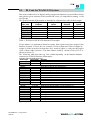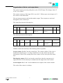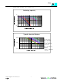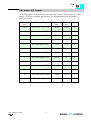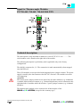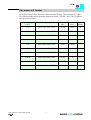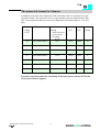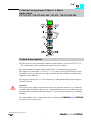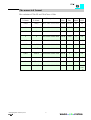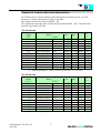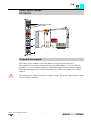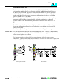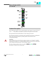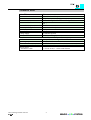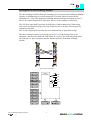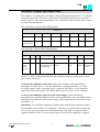
1
Modular I/O System INTERBUS S Manual Technical description, installation and configuration 750-132 Version 2.2.2 ii • General Copyright ã 1997-2001 by WAGO Kontakttechnik GmbH All rights reserved. WAGO Kontakttechnik GmbH Hansastraße 27 D-32423 Minden Phone: +49 (0) 571/8 87 – 0 Fax: +49 (0) 571/8 87 – 1 69 E-Mail: [email protected] Web: http://www.wago.com Technical Support Phone: +49 (0) 571/8 87 – 5 55 Fax: +49 (0) 571/8 87 – 4 30 E-Mail: [email protected] Every conceivable measure has been taken to ensure the correctness and completeness of this documentation. However, as errors can never be fully excluded we would appreciate any information or ideas at any time. We wish to point out that the software and hardware terms as well as the trademarks of companies used and/or mentioned in the present manual are generally trademark or patent protected. Modular I/O System INTERBUS S TABLE OF CONTENTS • iii TABLE OF CONTENTS Section 1: Explanations Section 2: System Description INTERBUS S, Configuration, Initial Starting, Diagnosis Section 3: Digital Inputs 750-400, 750-401, 750-402, 750-403, 750-405, 750-406, 750-410, 750-411, 750-408, 750-409, 750-412, 750-413, 750-414, 750-415 750-404 Section 4: Digital Outputs 750-501, 750-502, 750-504, 750-516, 750-519 750-506 750-509 750-511 750-512, 750-513, 750-514, 750-517 Section 5: Analog Inputs 750-452, 750-454, 750-482, 750-484 750-456, 750-461, 750-481 750-462, 750-469 750-465, 750-466, 750-486, 750-467, 750-468, 750-487, 750-488 750-472, 750-474 750-476, 750-478 Section 6: Analog Outputs 750-550, 750-580 750-552, 750-554, 750-584 750-556 Section 7: End- and Supply Terminal Blocks 750-600, 750-614, 750-616 750-601, 750-602, 750-609, 750-610, 750-611, 750-612, 750-613, 750-615 750-622 Section 8: SSI Encoder Interface, Quadrature Encoder Interface 750-630, 750-631 Section 9: RS232, TTY, RS485 750-650, 750-651, 750-653 Application in Explosive Environments Approvals Modular I/O System INTERBUS S iv • Notes Modular I/O System INTERBUS S IMPORTANT! For fast, trouble free installation and start up of the devices described in this manual, the user should carefully read and follow the advice and explanations offered in this guide. Explanation of symbols used: The EXCLAMATION POINT symbol is used when: a) improper handling could cause damage or destruction of the hard- or software b) possible injury to persons when interfacing to dangerous process peripherals. The FINGER symbol describes routines or gives advice for the efficient use of the devices and optimization of the software. FUNCTION The FUNCTION symbol refers to helpful notes which are necessary for the correct function. These remarks should be followed. The QUESTION MARK gives an explanation of terms. The symbol BOOKS gives references to additional literature, manuals and data sheets. The user is most important to us: We place great importance on the quality and user-friendliness of our manuals. Should you have any ideas or suggestions for improvement to the contents or graphical design, we would be glad to receive your proposals. Notice: This manual, including all illustrations, is copyrighted. Any use of this manual beyond the terms of copyright is not allowed. The reproduction, translation, or use of the electronic and mechanical information is subject to written authorization from WAGO Kontakttechnik GmbH. Violations will be prosecuted. WAGO Kontakttechnik GmbH reserves the right of alternation and changes. All rights in case of granting patents or protective rights are reserved to WAGO Kontakttechnik GmbH. In the case of non-WAGO products no reference to patent rights is given, but their existence is noted. The use of the products described in this manuals exclusively intended for experts trained in PLC programming or electrical engineering, who are familiar with the national electrical standards in force. WAGO Kontakttechnik GmbH and overseas subsidiaries will not accept any liability for faulty actions and damages which occur on WAGO or non-WAGO products when disregarding the information given in this manual. Any change made in WAGO hard or software (for example entries in a register) will result in an exclusion of liability on the part of WAGO Kontakttechnik GmbH. INTERBUS S / General information 1 :$*2Ç,2Ç6<67(0 Table of contents chapter 2 1 The WAGO I/O SYSTEM 1 2 Buscoupler Interbus S 2 2.1 Buscoupler-Hardware 2.2 Supply voltage - Electronics 2.3 Supply voltage - Field Side 2.4 Bus connection and station address 2 3 4 5 3 Enclosure and technical data 8 4 Interbus S 9 4.1 Interface Modules 4.2 Configuration software 9 10 5 Configuration of the fieldbus node in the master controller 11 5.1 Identification code 5.2 ID Code for WAGO I/O System 5.3 IBS CMD Software 5.4 Example of application 11 12 13 19 6 Starting of operation and diagnostics 21 7 General conditions 23 7.1 Tansport and storing conditions 7.2 Mechanical and climatic conditions 7.3 Isolation, class of protection and degree of protection 7.4 Electromagnetic compatibility 7.5 Power supply Use in Hazardous Environments Approvals INTERBUS S / General information 23 23 24 25 25 :$*2Ç,2Ç6<67(0 1 The WAGO I/O System The WAGO I/O SYSTEM consists of various components which are capable of providing modular and application specific fieldbus nodes for various fieldbusses. I11.1 Setting up a fieldbus node with the WAGO I/O SYSTEM General remark: A fieldbus node consists in principle of a fieldbus coupler at the front end, a number of special function modules and a termination module which is placed at the other end. 1 - Buscoupler The Buscoupler forms the link between the fieldbus and the field devices with their I/O functions. All control functions required for the faultless operation of the I/O functions are carried out by the coupler. The connection to different fieldbus systems is established by each of the corresponding Buscouplers, e.g. for PROFIBUS, INTERBUS S, II/O LIGHTBUS, CAN, ModBus etc. In this way a change of the fieldbus system is possible. 2 - Function modules In the function modules, the incoming process data ais converted. Corresponding to the different requirements, special function modules are available for a variety of functions. There are digital and analog inputs and outputs and modules for special functions. The modules are described in the following chapters. 3 - Termination module A termination module is needed for faultless operation of the node. The termination module is always placed as the last module in order to obtain a termination of the fieldbus node. This module has no I/O function. Interbus / Introduction 1 :$*2Ç,2Ç6<67(0 Assembly of the WAGO I/O System All components of the system can be snapped directly on a carrier rail according to EN 50022 (DIN 35). When snapping the analog or digital components onto the rail, no special sequence must be observed. The secure positioning and connection of the individual function modules and the coupler is provided by a snap-in system. This snap-in system provides automatic interlocking onto the DIN rail assembly. It is always possible to remove a function module or the Buscoupler from the assembly by pulling the orange pull-tab. Please note, that the power supply of the field side as well as the data transmission are interrupted. It has to be ensured that the interruption of PE will not put personnel or equipment in danger. With a CAGE CLAMP, conductors with a cross section of 0.08 to 2.5mm2 /AWG 18-14 can be connected. Vibration proof, fast and maintenance-free. You simply introduce a screwdriver or an operating tool into the operating slot under the clamping unit. The CAGE CLAMP spring is pressed down. You can now introduce the wire into the clamping unit. Withdraw the operating tool and the conductor is automatically clamped. Interbus / Introduction 2 :$*2Ç,2Ç6<67(0 The clamping force adjusts automatically to the conductor cross section. The flat clamping face of the CAGE CLAMP spring presses the conductor against the current bar without damage. Any deformation or movement of the conductor is compensated, thus eliminating the risk of a loose connection. The contact point between conductor and CAGE CLAMP is well protected against corrosive deterioration. This connection is made fast and, furthermore, it is maintenance-free. There is no need for costly periodical examination of the connections. The supply modules of the WAGO I/O system are partly equipped with a fuse holder. This fuse holder can be pulled out in order to break the circuit of the following modules. To do so, you first have to insert a screwdriver into one of the slots on both sides in order to pull out the front side of the fuse holder. The front side now being hinged down makes it possible to remove or to insert the fuse. After that, you lift up the front side again and push the fuse holder back into its original position. Interbus / Introduction 3 :$*2Ç,2Ç6<67(0 2 Buscoupler - INTERBUS S 2.1 Buscoupler - Hardware Ill. 2: The INTERBUS buscoupler The 750-304 Interbus coupler consists of two major electronic sub systems: left side: This housing contains the electronics for the coupling to the bus, the processor and the fieldbus connection. (ill. 2.1) right side: This housing contains the DC to DC converter and power distribution for the internal K bus, local processor and external 24 V DC connections to other discrete I/O modules. Illustration 2.2 identifies the 24 V DC connection points to supply voltage to I/O modules. Illustration 2.3 identifies the ground connection. INTERBUS S / Buscoupler 3 :$*2Ç,2Ç6<67(0 2.2 Supply Voltage - Electronics Ill. 3: Termination points for the power supply and the internal electronics The nominal operating voltage of the Buscoupler and the control electronics in the function modules is 5 V DC. The supply is connected to the first two CAGE CLAMPS at the top of the coupler as seen in Ill. 3. The 24 V DC supply voltage is generated by an internal voltage regulator (DC/DC converter) and fed to the electronics (5 V DC). The electrical isolation of the external bus system is made by utilizing an optocoupler. Please note that the power supply for the control electronics in the function modules is made automatically by the data contacts of the following module when it is snapped on the assembly (ill. 3.1). The power supply to the attached I/O modules is provided by gold-plated self-cleaning slide contacts. I f an attached module is taken out of the existing configuration, the connection via the K bus is broken and the coupler is able to detect this. WARNING If a module is taken out of the ex isting configuration, there may be undefined states. You should disconnect the power supply when changing anything in the configuration. INTERBUS S / Buscoupler 4 :$*2Ç,2Ç6<67(0 2.3 Supply Voltage - Field Side Ill. 4: Termination points for the supply voltage - Field side The connection of the supply voltag e is electrically isolated from the internal electronics. Two CAGE CL AMPS are alway s connected by a power contact. By this way, the power supply is taken to different points of the configuration. It is possible to supply the following at the termination points (Ill. 4): Volts: 24 V DC - Amps: 10 A DC WARNING! 120 and 230 V AC can only be supplied via modules 750-609, 750-611 and 750-612! The supply modules which are permanently integrated on the buscouplers, can be supplied with 24 V DC only. The current on the power contacts should be max. 10 A. The voltage is automatically supplied when the function modules are snapped together. Self-cleaning power jumper contacts (P.J.C.s) ensure safe connections (Ill. 4). Female contacts (current supply) are integrated in the buscoupler and I/O housings. The male contacts on the buscoupler and I/O housings supply the voltage to the I/O modules when inserted together from left to right. The ground (earth) contact makes first and breaks last conforming to electrical standards and can be used as protective grounding. Depending on the I/O function, some modules do not have P.J.C.s. It is important to note this when assembling a node. Many modules require field side power, many do not. Please review the circuit diagrams of the individual modules. An additional power supply module may be necessary. INTERBUS S / Buscoupler 5 :$*2Ç,2Ç6<67(0 When using the supply module 750-601/602, the field supply from the bus coupler is interrupted. From that point a new power supply connection is necessary to provide DC to any additional I/O modules. WARNING! The ground ( earth) field side contact should be disconnected when testing the isolation. Otherwise the results could be wrong or even the module could be destroyed. INTERBUS S / Buscoupler 6 :$*2Ç,2Ç6<67(0 2.4 Bus connection and station (node) address Ill. 5: Bus connection Fieldbus connection: The Interbus interface is normally provided by D SUB connection according Standard EIA RS485 for data transmission by wires. Outgoing D-SUB (OUT) /DO DO /DI DI COM PIN cable PIN 6 1 7 2 3 5 9 green yellow pink gray brown commoning wire commoning wire 6 1 7 2 3 to US Incoming D-SUB (IN) /DO DO /DI DI COM Table 1: Wire connection Interbus S The connection point of the D SUB connector is lowered in such a way that after a connector is installed placement in an 80mm high switchbox is possible. INTERBUS S / Buscoupler 7 :$*2Ç,2Ç6<67(0 Configuration Interface The configuration interface used for the communication with WAGO-I/O-CHECK or for firmware upload is located behind the cover flap. Configuration interface Fig. X-1: Configuration interface g01xx06e The communication cable (750-920) is connected to the 4-pole header. Warning The communication cable 750-920 must not be connected or disconnected while the coupler/controller is powered on! INTERBUS 7a WAGO-I/O-SYSTEM 750 3 The Enclosure and Specifications SYSTEM DATA: Number of function modules Number of I/O points Transmission medium max. bus length Baud rate INTEBUS S / Enclosure and specifications 750-304 750-324 256 on request 4096 on request shielded Cu-cable (5 x 0.25 mm²) 400 m 500 kBaud 8 :$*2Ç,2Ç6<67(0 TECHNICAL DATA: Number of function modules Digital peripheral signals Analog peripheral signals Configuration possibility Bus connection Voltage supply Input current Internal current Power jumper contacts Maximum current supplied to K-Bus for internal module use Voltage power jumper contacts Current power jumper contacts Data contacts 750-304 750-324 dig.+analog digital 64 32 256 64 32 --via PC or control --2 D-SUB with protection against vibration 24V DC (-15%/+20%) 105 mA typ; 900 mA max. 85 mA typ.; 500 mA max. 400 mA 400 mA blade / spring contact slide contact, self-cleaning 1.75 A on request 24 V DC 10A DC slide contacts, 1.5 u hard gold-plated self-cleaning <1V with 64 wired special function modules Polycarbonat, Polyamid 6.6 standard markers WAGO BR247/248 marker cards 8 x 47mm CAGE CLAMP; 0.08mm2 -2.5mm2 /AWG 28 -14 any position IP 20 500 V system / power supply 0°C...+55°C 51 x 65* x 100 (*from upper edge of the carrier rail) Voltage drop via data contacts Housing material Marking Wire connection Mounting position Type of protection Isolation Operating temperature Dimensions (mm) W x H x L INTEBUS S / Enclosure and specifications 9 :$*2Ç,2Ç6<67(0 Interbus S buscoupler with extended diagnostics 750-304/000-001 The Interbus S buscoupler with no. 750-304/000-001 has the possibility of extented diagnostic functions. The technical data is the same as 750-304. Different from the standard buscoupler, a word for diag nostic messages is put into the input data process image and a word for the control of the diag nostic input is put into the output data process image. The maximum number of input and output modules is reduced by the additional diagnostic function because Interbus S transmits only 31 words of a process image. Order of the diagnostic status word: Bit of the 15 14 13 12 11 10 9 status word error error code (s. table) 8 7 6 5 4 3 2 1 0 Channel Module The error code is shown in the following table: Error code 0 5 10 15 Description unknown fault defective fuse broken wire short circuit Channel: This is the location for the fault input of a module. The counting is done in the same way as numbering channels. Module: This is the number of the module. Counting starts at the fieldbus coupler. The first module attached to the coupler is module 0. The diagnostic control word is for diagnostic actions. E.g. error messages can be cleared in this way. Order of the diagnostic control word: Bit of the 15 14 13 12 11 10 9 control word Actions 8 7 6 5 4 3 2 1 0 The actions are coded as follows: Actions 0x00 (0) 0x01 (1) 0x80 (128) INTEBUS S / Enclosure and specifications Description no action Acknowledge diagnostic control word Clears all error messages in the buffer 10 :$*2Ç,2Ç6<67(0 4 INTERBUS S The Interbus S system (DIN 19245 part 1.2) is set up as a data ring with a central master slave access procedure. All modules are understood as one log ical module. Each partner receives data at its input and sends it to the nex t partner at its output. There is no addressing with a data frame because each partner knows by special control sig nals (CLOCK, RESET, SELECT, CONTROL) where it is placed in the ring. So there is no bus address. „Addressing“ is done via the physical place in the system. Interbus S has the structure of a spatially distributed shift reg ister. Each cycle is input and output at the same time. While the master g ives output data to the shift register, it gets input data from the other end of the ring. Each part of Interbus S has an ID register. This register keeps information about the type of module, the number of I/O registers and the status and error information. Interbus S has two general operating modes: 1) ID cycle The interface module of all devices connected to the bus system reads out the ID register in the ID cycle and builds up the process imag e with the aid of this information. The cycle serves as an initialization and is carried out on request. 2) Data cycle Within the data cycle all input data from the registers is transferred from all devices into the master card (Host Controller) and all output data from the master card (Host controller) to the devices. 4.1 Master Cards (Scanners, Host Controllers) The operation of the master is carried out in most cases via a central controller like a PLC, PC or NC. Connection to the remote stations is made via master cards. Common master modules are: - Phoenix IBS S5 DCB/I-T - Phoenix IBS S5 DSC/I-T - Phoenix 100 CB-T - Hilscher CIF 30 (via Synergetic Micro Systems in USA) INTERBUS S / Interbus S 11 :$*2Ç,2Ç6<67(0 4.2 Configuration software In order to make the connection between a PLC or PC and the remote stations, the master cards must be configured with the individual station data. For this, the following software packages are available. For example, the following are available from Phoenix: - IBS SYS SWT - IBS CMD SWT INTERBUS S / Interbus S 12 :$*2Ç,2Ç6<67(0 5 Configuration of the fieldbus node in the master 5.1 Identification Code In the ID cycle which is carried out for the initialization of the Interbus system, the users connected users are identified by their function and their byte length. The Interbus S coupler identifies its length after being started in the initialization phase of the bus modules and forms a corresponding ID code. To this effect each slave has an implemented identification register (ID register) comprising 2 bytes. A 2 byte wide data unit is called a word. It enables the encoding of 65536 different states. In Interbus S, different types of users and data widths are called for the coding. This enables the master to find out what type the device belongs to, which means for example, recognizing either frequency inverters or I/O units, like the :$*2Ç,2Ç6<67(0 In Interbus S the manufacturers of device types are not recognized. The structure of the ID code is explained below as well as the significance of the individual bits of the ID code. The length information can be coded from 0 to 32 words: 15 14 13 12 11 10 9 8 7 6 5 4 3 2 1 0 messages data width class of user type of user data direction I, O, I/O Table 2: Structure of the Interbus ID code -In the ID registers, the device group is coded in the lowest value (L SB) 8 bits (ID 0 to 7). -In the following 5 bits (ID 8 to 12), the data width is coded. The 3 bits with the highest value (MSB) (ID 13 to 15) are used for manag ement functions. Via these bits, dy namic fault messages are transferred during operation. These bits are not defined by the hardware. INTERBUS S / Configuration 13 :$*2Ç,2Ç6<67(0 5.2 ID Code for WAGO I/O System Due to the combined use of dig ital, analog and special functions on one fieldbus station and with the given structure of the I nterbus ID codes, it is impossible to manag e with one ID code. The WAGO Interbus S buscoupler is identified as a digital slave with variable length! ID-Code dec, hex 1, 0x1 2, 0x2 3, 0x3 49, 0x31 50, 0x32 51, 0x33 Digital Outputs x Digital Inputs Analog Outputs Analog Inputs x x x - x - - x x x [x]: ID code given []: is not possible [-]: when mixed with digital Table 3: ID codes for the WAGO Interbus S buscoupler For the master, it is important to know how many data registers each user assigns in the Interbus S system. If a user has, for example, 16 bits of input and 32 bits of output, he assigns 2 words in the bus because there are 2 words of output. I n this case the hig her value of data width is decisive. The data width is coded by the bits I D 8 to I D 12 as shown in section 5.1. The following table shows the reg ister widths depending on the function modules connected to a WAGO Interbus S buscoupler. Possible values for data length are:: Data length Buscoupler Remarks 0 Words x 1 Nibble Busmaster supports only Generation 4. 1 Byte Starting with SPS-Firmware 3.20 or PC-driver 2.0 3 Nibble Busmaster supports only Generation 4 1 Word x 3 Nibble Busmaster supports only Generation 4 3 Byte Starting with SPS-Firmware 3.20 or PC-driver 2.0 2 Words x 5 Nibble Busmaster supports only Generation 4 5 Byte Starting with SPS-Firmware 3.20 or PC-driver 2.0 3 Words x 4 Words x 5 Words x 6 Words x, ab WF Starting with SPS-Firmware 3.20 or PC-driver 2.0 7 Words x, ab WF Starting with SPS-Firmware 3.20 or PC-driver 2.0 8 Words x 9 Words x 10 Words xx Starting with SPS-Firmware 3.20 or PC-driver 2.0 12 Words xx Starting with SPS-Firmware 3.20 or PC-driver 2.0 14 Words xx Starting with SPS-Firmware 3.20 or PC-driver 2.0 16 Words xx Starting with SPS-Firmware 3.20 or PC-driver 2.0 24 Words xx Starting with SPS-Firmware 3.20 or PC-driver 2.0 32 Words xx Starting with SPS-Firmware 3.20 or PC-driver 2.0 [x]: is used [xx]: is used and firmware 3.20 or PC driver 2.0 or later is combined INTERBUS S / Configuration 14 :$*2Ç,2Ç6<67(0 5.3 IBS CMD configuration software In the following chapter the configuration package IBS CMD configuration software is presented in short form. This procedure facilitates operation of the WAGO Interbus buscoupler. Further and specific information is given in the respective operating instructions of the different software packages. 5.3.1 CMD Software Package Please pay attention that the corresponding interfacing and the function extended should be selected. The following menu is obtained via the key OK and the password allocated at the program installation. Ill. 10: First menu configuration This is the first menu for further configuration. From this point the configuration can be made automatically or manually. INTERBUS S / Configuration 15 :$*2Ç,2Ç6<67(0 1) Automatic configuration Ill. 11: Automatic configuration If the complete fieldbus system with all stations and the master interface is operational, automatic configuration of the connected stations can be called up via the menu „bus structure“. Then the communications are started automatically and the configuration is determined and set. INTERBUS S / Configuration 16 :$*2Ç,2Ç6<67(0 2) Ident code Ill. 12: Insertion of the WAGO I/O System via the Ident code For manual configuration, the menu item „ bus structure“ in the config uration screen must be selected. You will then see Ill. 12. The corresponding ID code of table 3 and the length of the process data channel must be indicated in the selected submenu. The length is dependent on the module with the largest data length. INTERBUS S / Configuration 17 :$*2Ç,2Ç6<67(0 Ill. 13: Insertion of the ID code and the data length With the finalization of the entries via the key OK, a menu for the definition of the user will appear. INTERBUS S / Configuration 18 :$*2Ç,2Ç6<67(0 Ill. 14: Description of user INTERBUS S / Configuration 19 :$*2Ç,2Ç6<67(0 After all data has been entered and stored via OK, the station created with the WAGO Interbus coupler is then integrated into the fieldbus system being set up. This station is displayed via the bus structure that has now been integrated: INTERBUS S / Configuration 20 :$*2Ç,2Ç6<67(0 5.4 Example of an application Ill. 19: Example of an application The Interbus S station is composed as follows: Function module 1; Digital input 1; Digital Input 2; Digital Input 2; Digital Input 3; Voltage supply 4; Analog Input 4; Analog Input 5; Voltage supply 6; Digital Output 6; Digital Output 7; Digital Output 7; Digital Output 8; Digital Output 8; Digital Output 9; Digital Output 9; Digital Output 10; Voltage supply 11; Analog Output 11; Analog Output 12; Analog Input 12; Analog Input 13; Analog Output 13; Analog Output 14; Analog Input 14; Analog Input 15; Voltage supply 16; Digital Output 16; Digital Output 17; End module Process image inputs PI 32.0 PI 32.1 PI 32.2 PI 32.3 -----PI 20 PI 22 ------ -----PI 24 PI 26 PI 28 PI 30 ------ Table 5: Assignment of the process image INTERBUS S / Configuration 21 ------ Process image outputs ----------PI28.0 PI28.1 PI28.2 PI28.3 PI28.4 PI28.5 PI28.6 PI28.7 -----PI 20 PI 22 PI 24 PI 26 -----PI29.0 PI29.1 ------ :$*2Ç,2Ç6<67(0 The addresses indicated in the table results from the master configuration started in the basic address. By the internal structure of the Interbus coupler, the process image is divided as follows: O0 Output data .... .....word orientated data .... Ox Ox+1 bit orientated data Ox+y Input data I0 .... ....word orientated data .... Ix Ix+1 bit orientated data Ix+y Due to this division, the first addresses allocated in the configuration are reserved for the analog inputs and outputs. The counting direction is from left to right and starts with the first analog channel next to the bus coupler. Ill. 21: Definition inputs/outputs INTERBUS S / Configuration 22 :$*2Ç,2Ç6<67(0 6 Buscoupler startup and troubleshooting After configuration of the master connection and electrical installation of the fieldbus node/station, operation of the system can begin. After power to the B uscoupler and I /O modules has been applied, the B uscoupler verifies all internal functions, components and the communication interface by an internal diagnostic routine. Then the function modules and the existing configuration is determined. At the same time a hidden file is stored. It consists of an input and an output area which is located on the fieldbus RAM of the log chip. During the power up phase the ‘I/O ERR’ LED flashes with an increased frequency . After a faultless power up the fieldbus coupler enters the state ‘fieldbus start’. The g reen LED ‘RUN’ indicates that the Bus is operating normally. In case of a fault the red ‘I/O ERR’ LED will continue flashing. By counting the number and frequency of flashes the fault can be easily identified quickly and accurately. A varying number of flashes and frequencies defines the fault. The table below describes the fault condition based on the counted number of ‘I/O ERR’ LED flashes. ,2581 ,2(55 VHTXHQFH 3DXVH 2. Blinking sequence 3. Blinking sequence error code error argument 1 0 2 VHTXHQFH 3DXVH VHTXHQFH description 1 overflow of internal buffer for inline code 2 unknown data type 0 error in programmed process image error in comparison of tables: module N (programmed configuration), passive modules like supply terminal blocks do not count N (N>0) 3 0 modules have identified error in fieldbus commands 4 0 data error on fieldbus or fieldbus break at the coupler 4 N (N>0) 5 N fieldbus break after module N filedbus error in register communications with module N error in INTERBUS-S configuration telegram 6 too lillte configuration data 0 error in 1st configuration byte N (0<N<65) Table 5: Diagnosis LEDs - on buscoupler INTERBUS S / Startup 23 :$*2Ç,2Ç6<67(0 After elimination of the fault, the buscoupler can only be set to the normal working condition by another POWER ON sequence. The green I/O LED flashes when accessing the I/O modules internal data channels. After being switched on, the buscoupler queries the configuration of the bus modules but does not carry out a data exchange with the I/O modules. This means that the red I/O LED will extinguish after a faultless startup. The green I/O LED will indicate when data is being exchanged by the Interbus network. Status and error diagnostics: The fieldbus LEDs show the state of the bus system. The functions of Interbus S are shown by the LEDs „READY“, „BA“, „RC“ and „RD“. READY BA RC RD Meaning on off off off Buscoupler ready on on off off Fieldbus active; data exchange on off on off incoming connection established on off off on off off off off Field bus off error in cable or master no function ; no voltage Help search error in cable or master Table 7: Diagnostic LEDs - fieldbus INTERBUS S / Startup 24 :$*2Ç,2Ç6<67(0 7 General conditions This chapter describes the general conditions for error-free running of the :$*2Ç,2Ç6<67(0 7.1 Transporting and storing conditions The following declarations concern modules which are transported and stored in the original package. Condition Free fall Temperature Relative humidity allowed values ≤ 1m -40° to +70° C 5 to 95% (without condensation) 7.2 Mechanical and climatic conditions The modules of the :$*2Ç,2Ç6<67(0 are not allowed to be operated without taking suitable actions - in places with strong conditions e.g. very dusty rooms or corroding atmosphere - in place with high concentrations of ionisation The temperature should be in a range between 0° C and +55° C. The relative humidity should be in a range of 5 to 95% (without condensation). The modules should be placed horizontal for better heat dissipation. The concentration of SO2 must be below 25 ppm with a relative humidity of < 75%. The concentration of H2S must be below 10 ppm with the same humidity. The mechanical conditions are given as sinusoidal oscillations. Frequency range (Hz) 10 ≤ f < 57 57 ≤ f ≤ 150 continuous 0.0375 mm amplitude 0.5 g constant acceleration sometimes 0.075mm amplitude 1 g constant acceleration For stronger impulses and oscillations, the acceleration and the amplitude should be reduced by suitable actions. The following table shows the type of test for the mechanical conditions. INTERBUS / General conditions 25 :$*2Ç,2Ç6<67(0 Test for Oscillations Impulse 7.3 Test sequence Remarks Test for oscillations Type of oscillation: sweep with a rate of IEC 68, part 2-6 change of 1 octave per minute 10 Hz ≤ f < 57 Hz, const. amplitude 0,075mm 57 Hz ≤ f ≤ 150 Hz, const. acceleration 1g period of oscillation: 10 sweep per axis in each of the 3 vertical axes Test for impulses Type of impulse: half sinusoidal IEC 68, part 2-27 Intensity of impulses: 15 g peak value, 11 ms maintenance time route of impulses: 2 impulses in each of the 3 vertical axes Class of protection and degree of protection The class of protection is IP2X (IEC 529), i.e. protection against touch with a standard test object. There is also protection against solid bodies greater than 12 mm. There is no special protection against water. INTERBUS / General conditions 26 :$*2Ç,2Ç6<67(0 7.4 Electromagnetic compatibility Method of measurement Interference with narrow-band conducted disturbance Interference with impulse groups Discharge of static electricity Interference with electromagnetic fields Interference field strength Disturbance EN 50082-2, A EN 50082-2, B EN 50082-2, B EN 50082-2, A EN 55011 These requests for electromagnetic compatibility are fulfilled by all modules of :$*2Ç,2Ç6<67(0(except for 750-630 and 750-631). 7.5 Power supply If non-stabilized power supply is used for the supply of the buscoupler, it must be stabilized by a capacity ( 200 µF per 1 A load current). For the :$*2Ç,2Ç6<67(0a filter module has been developed (288-824). This module serves as a filter module for non-stabilized 24 V DC power supplies if the specified voltage deviation is not met. Reasons for the deviations may be voltage jumps in the primary circuit, overloads in the secondary circuit or the switching of undampened inductances and capacitances. 7.6 Certificates The modules of :$*2Ç,2Ç6<67(0 have passed the conformance test of UL . Look for listing mark on product. The Profibus coupler 750-301 and 750-303 are certified of PNO with Z 00241 and Z00242. The Interbus coupler 750-304 has passed the relevant tests in accordance with the Interbus conformance requirements (number 111). The DeviceNet coupler 750-306 has succesfully passed through the conformance test of Open DeviceNet Vendors Association Europe. INTERBUS / General conditions 27 :$*2Ç,2Ç6<67(0 Digital Inputs (24 V AC/DC, 120 V AC, 230 V AC, 48 V DC) PN: 750-400...415 Technical description The supply is applied by a series-connected termination to each I/O module for the respective operating voltage. Power connections are made automatically from module to module when snapped onto the DIN rail. Attention: The lowest power jumper contact is not carried out for some modules (e.g. 4-channel)! A module which needs all contacts (e.g. 2 channel digital) may not be connected to the right hand side of modules which do not have 3 power jumper contacts (e.g. 4 channel modules). All 2-channel digital inputs are 4-conductor devices allowing the direct connection of 4conductor sensors with the terminations V+, 0V, ground and signal. The 4-channel digital inputs are suitable for the direct connection of two 3-conductor sensors (V+, 0V, signal). The power distribution module 750-614 is available for the connection of more sensors to V+ and 0V. The modules 750-408 and 750-409 are low-side switching. A 2-wire proximity switch can be connected to the modules 750-410 and 750-411. RC filters are series-connected to the 5, 24 and 48 V versions for noise rejection and switch debouncing. They are available with time constants of 3.0 ms and 0.2 ms. The standard numerical assignment for bus operations is from left to right, starting with the LSB. The positions of the different I/O modules in the configured node/station are selectable by the user. A block type configuration is not necessary. The Input module can be connected to all buscouplers of the WAGOÇI/OÇSYSTEM. Digital Inputs 750-400...415 1 :$*2Ç,2Ç6<67(0 Technical Data: Item Number 750Number of inputs Input filter Nominal voltage Signal voltage (0) Signal voltage (1) Input current (internal) Input current (field side) Isolation Internal bit width Configuration Operating temperature Wire connection Dimensions (mm) WxHxL Item Number 750Number of inputs Input filter Nominal voltage Signal voltage (0) Signal voltage (1) Input current (internal) Input current (field side) Isolation Internal bit width Configuration Operating temperature Wire connection Dimensions (mm)WxHxL 400 402 403 4 0.2 ms 3 ms 0.2 ms 24V DC (-15%/+20%) -3V...+5V DC (std. EN 61131 Typ 1) 15V...30V DC (std. EN 61131 Typ 1) 2.5 mA max. 5 mA max. 5 mA typ. 500 V system/power supply 2 4 no address or configutation adjustment 0°C....+55°C CAGE CLAMP; 0.08 to 2.5mm2 12 x 64* x 100 (*from upper edge of carrier rail) 3 ms 2 401 405 406 2 10 ms 230 V AC 120 V AC (-15%/+10%) (15%/+10%) 0 V...40 V 0 V..20 V AC AC 79 V...1.1 UN 79 V...1.1 AC UN AC 2 mA 6.5 mA typ. 4.5 mA typ. 4 kV system/power supply 410* 2 411* 3 ms 0.2 ms 24V DC (-15%/+20%)) -3 V ... +5 V DC (std. EN 61131 Type 2) 11 V ... 30 V DC (std. EN 61131 Type 2) 2.5 mA max. 8 mA typ. 500 V system/power supply 2 no address or configuration adjustment 0°C....+55°C CAGE CLAMP; 0.08 to 2.5mm2 12 x 64* x 100 (*from upper edge of the carrier rail) *) 2 - wire proximity switch, current without load max. 2 mA Digital Inputs 750-400...415 2 :$*2Ç,2Ç6<67(0 Item Number 750Number of inputs Input filter Nominal voltage Signal voltage (0) Signal voltage (1) Input current (internal) Input current (field side) Isolation Internal bit width Configuration Operating temperature Wire connection Dimensions (mm)WxHxL Item Number 750Number of inputs Input filter / Conversion time Nominal voltage Signal voltage (0) Signal voltage (1) Input current (internal) Input current (field side) Isolation Internal bit width Configuration Operating temperature Wire connection Dimensions (mm)WxHxL Digital Inputs 750-400...415 408 4 409 412 2 413 3 ms 0,2 ms 3 ms 0,2 ms 24V DC (-15% / +20%) 48 V DC (-15% / +20%) 15 V...30 V DC -6 V ... +10 V DC -3 V...5 V DC 34 V ... 60 V DC 10 mA max. 5 mA max. 3.5 mA typ. 500 V system/power supply 4 2 no address or configuration adjustment 0°C....+55°C CAGE CLAMP; 0,08 to 2,5 mm2 12 x 64* x 100 (*from upper edge of the carrier rail) 414 4 0.2 ms 415 4 20 ms 5 V DC 24 V AC/DC (-15%/+20%) 0...0.8 V DC -3...+5 V DC 0...+5 V AC 2.4 V...5 V DC 11 ... 30 V DC 10 ... 27 V AC 5 mA 10 mA 50 µA typ. 7.5 mA DC 7.6 9.5 mA AC 500 V system/power supply 500V system/power supply 50 V channel/channel 4 4 no address or configuration adjustment 0°C....+55°C CAGE CLAMP; 0,08 to 2,5 mm2 12 x 64* x 100 (*from upper edge of the carrier rail) 3 :$*2Ç,2Ç6<67(0 Counter modules PN 750-404, 750-404/000-001, 750-404/000-002 750-404/000-003, 750-404/000-004 Up/Down Counter 100 kHz, 750-404 Technical Description: Attention! The description that is in the I/O ring binder data pages (88-530/013-600 dated 7/96) is not correct. The bottom contacts are additional outputs. Attention: The lowest power jumper contact is not carried out for some modules (e.g. 4-channel)! A module which needs all contacts (e.g. 2 channel digital) may not be connected to the right hand side of modules which do not have 3 power jumper contacts (e.g. 4 channel modules). The described configuration is counter with up/down input. The following description is preliminary and is applicable to the factory configuration. The counter module is able to run with all WAGOÇI/OÇSYSTEM bus-couplers (except for the economy type). Counter Module 750-404 1 :$*2⇓,2⇓6<67(0 Technical Data: Item Number: 750Number of outputs Output current Number of counter Input current (internal) Nominal voltage Signal voltage (0) Signal voltage (1) Switching rate Output current Counter size Isolation Bit width Configuration Operating temperature Wire connection Size (mm)WxHxD Counter Module 750-404 404, 404/000-001 404/000-004 404/000-002 2 0.5 A 1 70 mA 24 V DC (-15% +20%) -3V.....+5V DC +15V...+30V DC 100 kHz 10 kHz max. 5 mA typ. 32 Bit 500 V system/power supply 32 Bit (8 Bit verification; 8 bit not used) none, optional with software parameter 0°C....+55°C CAGE CLAMP; 0.08 to 2.5mm2 12 x 64* x 100 (*from upper edge of the carrier rail) 2 :$*2⇓,2⇓6<67(0 Organization of the in- and output data: The counter begins processing with pulses at the CLOCK input. The changes from 0 V to 24 V are counted. The counter counts up, if the input U/D is set at 24 V. With an open circuit input or 0 V the counter counts backwards. The two bottom contacts each include another output. These outputs are activated through bits in the control byte. The control byte has the following bits: Control Byte Bit 7 Bit 6 Bit 5 Bit 4 Bit 3 Bit 2 Bit 1 Bit 0 0 x Set Counter Block Counter Output value at output O2 Output value at output O1 x x The status byte has the following bits: Status Byte Bit 7 Bit 6 Bit 5 Bit 4 Bit 3 x x Counter is Counter is actual signal at set blocked O2 Bit 2 Bit 1 Bit 0 actual signal at O1 actual signal at input U/D actual signal at input CLOCK With the control and status-byte the following tasks are possible: Set the counter: Put Bit 5 into the control byte. The counter with the 32 bit value is loaded into output bytes 0-3. As long as the bits are set, the counter can stop and information is stored. The ensuing data of the counter will be conveyed to the status byte. Blocking the counter: Bit 4 is set into the control byte, then the count process is suppressed. Bit 4 in the status byte communicates the suppression of the counter. Set the outputs: Bits 2 and 3 set the additional two outputs of the counter module. The result of the counter is in binary. Counter Module 750-404 3 :$*2⇓,2⇓6<67(0 An example: The counter is set with “Set Counter” to the value 0x0000.0000 - 0X1X.XXXX, 0x00, 0x00, 0x00, 0x00 are carried over as output value (carry over the control-byte and the new counter position), -wait until the input value is 0X1X.XXXX, 0x00, 0x00, 0x00, 0x00 (the status-byte shows the loading feedback) , -carry over 0x00, 0x00, 0x00, 0x00, 0x00 as output value (release counter). Wait for the first and further counting pulse -the input value is XX00.XXXX, 0x00, 0x00, 0x00, 0x00 (no counting pulse received) -the input value is XX00.XXXX, 0x00, 0x00, 0x00, 0x01 (1 counting pulse received) -the input value is XX00.XXXX, 0x00, 0x00, 0x00, 0x02 (2 counting pulses received) -................. -the input value is XX00.XXXX, 0xFF, 0xFF, 0xFF, 0xFF (maximum counting position is reached) -the input value is XX00.XXXX, 0x00, 0x00, 0x00, 0x00 (a further counting pulse causes an overflow) -the input value is XX00.XXXX, 0x00, 0x00, 0x00 0x01, (a further counting pulse is received) Notes: Counter Module 750-404 0x23 is a value in hexadecimal form 0101.1001 is a value in binary form “X” is used if the value at this position is without any significance. 4 :$*2⇓,2⇓6<67(0 Counter with enable input 750-404/000-001 Technical description: The counter module also can be ordered as counter with enable input (750-404/000001). The counter begins processing with pulses at the CLOCK input. The changes from 0 V to 24 V are counted. The counter counts down if the input U/D is set at 24 V. With an open circuit input or 0 V the counter counts up. The data format of the module is 4 bytes data and a control/status byte. The module is a 32 Bit counter. The ID Code os 180 (0xB4). The format of input and output data is the same as 750-404. The counter module is able to run with all WAGOÇI/OÇSYSTEM bus-couplers (except for the economy type). Counter Module 750-404 5 :$*2⇓,2⇓6<67(0 Peak Time Counter 750-404/000-002 Technical data The counter module also can be ordered as peak time counter with 750-404/000-002. This description is only intended for hardware version X X X X 0 0 0 1- - - -. The serial number can be found on the right side of the module. The counter begins processing with pulses at the CLOCK input. The changes from 0 V to 24 V are counted. The counter counts up if the input U/D is set at 24 V. With an open circuit input or 0 V the counter counts backwards. The two bottom contacts each include another output. These outputs are activated through bits in the control byte. The counter module is able to run with all WAGOÇI/OÇSYSTEM bus-couplers (except for the economy type). Counter Module 750-404 6 :$*2⇓,2⇓6<67(0 Organization of the in- and output data: The counter begins processing with pulses at the CLOCK input for a special time span. The time span is predefined as 10 s. The state of the counter is stored in the processs image until the next period. After the recording the counting starts again at 0. The activation of the counting and the synchronisation with the SPS is made by a handshake in the control and status byte. The end of thre counting period and thus the new process data is signaled by a toggel bit in the status byte. The control byte has the following bits: Control Byte Bit 7 Bit 6 Bit 5 Bit 4 Bit 3 Bit 2 Bit 1 Bit 0 0 0 start of the periodic counting 0 Output value at output O2 Output value at output O1 0 0 The status byte has the following bits: Status Byte Bit 7 Bit 6 Bit 5 Bit 4 Bit 3 Bit 2 Bit 1 Bit 0 0 0 counting started 0 actual signal at O2 actual signal at O1 actual signal at input U/D Toggelbit for end of the record Counter Module 750-404 7 :$*2⇓,2⇓6<67(0 Frequency Counter Module, 750-404/000-003 Status CLOCK Status Gate Q2 O1 O2 Q1 G Clk +E2 Clock Gate + + 24V 24V 24V - 0V- 0V 0V power jumper contacts O1 O2 Q1 Q2 S S O1Q1 O2 Q2 750-404 000-003 Technical Description The counter module 750-404/000-003 measures the period of the 24 V DC input sig nal at the CL OCK terminal and converts it into a corresponding frequency value. The measurement is enabled if the GATE terminal is an open circuit input or 0V. To disable processing, the GATE input is to be set to 24 V DC. The terminals O1 and O2 work as binary outputs. Each output can be activated via specific bits in the CONTROL byte. The high states of the input and output channels are each indicated by a LED. To recognize low frequency or near zero frequency signals, the maximum time between two data updates is parameterizable. Counter Module 750-404 8 :$*2⇓,2⇓6<67(0 Technical Data: Item-No.: 750Supply Voltage Input Voltage (low) Input Voltage (high) Input Current Min. Pulse Width Output Current Voltage Drop Frequency Range: Integration time = 1 period Integration time = 4 periods Integration time = 16 periods Measuring Error: Range 0.1 - 100 Hz Range 1 - 1000Hz Range 10 - 10000Hz Data Format: Process Image Internal Bit Width Input Current (internal) Operating Temperature Wire Connection Size (mm) WxHxD 404/000-003 24V DC (-15%/+20%) -3V - 5V DC 15V - 30V DC 5mA typ. at 24V DC 10µs 0.5A (short circuit protection) 0.6V DC max. at 0.5A 0.1 100Hz, Resolution 0.001Hz 1 - 1,000Hz, Resolution 0.01Hz 10 - 10,000Hz, Resolution 0.1Hz (1Hz) < ± 0.05% < ± 0.05 % < ± 0.2 % 5 Byte In- and Output 8 Bit CONTROL/STATUS + 32 Bit DATA 80mA max. at 5V DC 0°C....+55°C CAGE CLAMP; 0.08 to 2.5mm2 12 x 64* x 100 (*from upper edge of carrier rail) Frequency Range: Integration time = 1 period Integration time = 4 periods Integration time = 16 periods Measuring Error: Range 0.1 8000Hz Range 0.25 - 32000Hz Range 1 - 100000Hz Counter Module 750-404 0.1 - 8,000Hz, Resolution 0.001Hz 0.25 - 32,000Hz, Resolution 0.01Hz 1 - 100,000Hz, Resolution 0.1Hz (1Hz) < ± 1% < ± 1.5 % < ± 1.5 % 9 :$*2⇓,2⇓6<67(0 Functional description The counter module acquires the time between one or more rising edges of the CLOCK input signal and calculates the frequency of the applied signal. The calculation and process imag e update are initiated every 1st, every 4th or every 16th rising edge depending on the integration time selected via the CONTROL byte. The first detection of a rising edge starts the cy clic period measurement and cannot provide a valid frequency value. I n this case the module will send 0x FFFFFFFFH for input information. The same input value is returned when a static hig h or static low signal is applied to the CLOCK input. If there are no sig nal changes seen at the CL OCK input, the module can be forced to update the process imag e after defined parameterizable time spans. I n this state the module will send the non valid value 0xFFFFFFFFH too. The following figures illustrate a process data cycle. 73 7 ,1387)5(4 '$7$9$/,' 352&(66'$7$ [)))))))) '' '' [)))))))) '' '' '' '' ,QSXW'DWD 73 I FXUUHQWSHULRG 7 0D[LPXPGDWDKROGWLPHSDUDPHWHUL]DEOH Figure 2: Timing diagram for process data update sequence (integration time = 1 period) 7 73 ,1387)5(4 '$7$9$/,' 352&(66'$7$ [)))))))) '' '' [)))))))) '' ,QSXW'DWD 73 I FXUUHQWSHULRG 7 0D[LPXPGDWDKROGWLPHSDUDPHWHUL]DEOH Figure 3: Timing diagram for process data update sequence (integration time = 4 periods) Counter Module 750-404 10 :$*2⇓,2⇓6<67(0 Structure of CONTROL and STATUS byte CONTROL Byte E 5(*B5(4 E E E 79'5(4 E 6(7B4 E 6(7B4 5(*B5(4 15':5 5(*B$ 5(*B$ 5(*B$ 5(*B$ E E 5$1*(B6(/ 5$1*(B6(/ 5(4 5(4 5(*B$ 5(*B$ Bit Description 5(*B5(4 5(*B$$ 79'5(4 6(7B4 6(7B4 5$1*(B6(/5(4 5$1*(B6(/5(4 $FFHVVWRWKHUHJLVWHUVWUXFWXUHLVUHTXHVWHGEEFRQWDLQWKHDGGUHVVRIWKHUHJLVWHU 5HJLVWHUDGGUHVV 5HTXHVWWRFKDQJHWKHPD[LPXPWLPHZLWKRXWYDOLGGDWD &RQWURO2XWSXW44RII4RQ &RQWURO2XWSXW44RII4RQ 6HOHFWLRQRIWKHLQWHJUDWLRQWLPHDQGWKHUHSUHVHQWDWLRQRIPHDVXUHGIUHTXHQF\YDOXH 6HOHFWLRQRIWKHLQWHJUDWLRQWLPHDQGWKHUHSUHVHQWDWLRQRIPHDVXUHGIUHTXHQF\YDOXH STATUS Byte Counter 750-404 E 5(*B$&. E E 67B*$7( E 79'$&. E 67B4 E 67B4 5(*B$&. 5(*B$ 5(*B$ 5(*B$ 5(*B$ E E 5$1*(B6(/ 5$1*(B6(/ $&. $&. 5(*B$ 5(*B$ Bit Description 5(*B$&. 5(*B$$ 67B*$7( 79'$&. 67B$ 67B$ 5$1*(B6(/$&. 5$1*(B6(/$&. $FNQRZOHGJPHQWWRWKHUHJLVWHUUHTXHVWEEFRQWDLQWKHDGGUHVVRIWKHUHJLVWHU 5HJLVWHUDGGUHVV 6WDWHRI*$7(LQSXW HQDEOHG GLVDEOHG $FNQRZOHGJPHQW79'FKDQJHG 6WDWHRIRXWSXW4 6WDWHRIRXWSXW4 $FNQRZOHGJPHQWWR5DQJH6HOHFWLRQ)UHTXHQF\YDOXHVDUHYDOLG $FNQRZOHGJPHQWWR5DQJH6HOHFWLRQ)UHTXHQF\YDOXHVDUHYDOLG 11 :$*2Ç,2Ç6<67(0 Structure of Input and Output data The input data contain the CL OCK frequency as a binary value. The representation depends on the RANGE_SEL bits in the CONTROL byte. Even the method of measuring is selected via these bits. The following table illustrates the different modes. 5$1*(B6(/ 5$1*(B6(/ 0HWKRGRIPHDVXUHPHQW 5HSUHVHQWDWLRQRIPHDVXULQJYDOXH ,QWHJUDWLRQRYHUSHULRG ,QWHJUDWLRQRYHUSHULRGV ,QWHJUDWLRQRYHUSHULRGV ,QWHJUDWLRQRYHUSHULRGV )UHTXHQF\LQ+] )UHTXHQF\LQ+] )UHTXHQF\LQ+] )UHTXHQF\LQ+] Attention: When a new frequency range is requested, the application has to wait for valid data until the RANGE_SEL ACK bits contain the new frequency range. The maximum delay can be calculated using the following formula TDmax= 2 * number of periods to be integrated actual frequency If the gate is enabled the input data contains the last valid frequency value. In this state the application cannot request a new range. The valid frequency range stretches from 0.1 Hz (100D) up to 10 kHz (100000D). To recognize static CL OCK signals, a watchdog timer is implemented. The default value for the timer is 10s. The timer resets on every Power On. The application is able to change the watchdog time during operation by using the CONTROL byte. This can be initiated by writing the corresponding value into the output bytes OUTPUT_DATA 1 a nd OUTPUT_DATA 0 be fore setting the TVD REQ bit in the CONTROL byte. The success of the parameter transfer is acknowledg ed by the module via the TVD ACK bit in the STATUS information. Attention: The range of the watchdog timer stretches from 0 to 16383ms (0x 0000H to 0x3FFFH) in steps of 1ms per digit. Values which raise the permitted range of the watchdog timer are masked with 0x3FFF. If the maximum possible frequency of the different ranges is raised (see the table with maximum frequency ratings), the module will return the non valid data 0xFFFFFFFFH. Counter 750-404 12 :$*2Ç,2Ç6<67(0 Organization of the in- and output data for Interbus Output value of the control unit: Byte D15-D0 D31-D16 D47-D32 Identification Control Byte Output Byte 0 Output Byte 2 Output Byte 1 Output Byte 3 Input value of the control unit: Byte D15-D0 D31-D16 D2D47-D32 Identification Status Byte Input Byte 0 Input Byte 2 Input Byte 1 Input Byte 3 The input-bytes 0 to 3 form the 32 bit counter-output. In the output-bytes 0 to 3 the initial value of the counter can be set. Counter 750-404 13 :$*2Ç,2Ç6<67(0 Digital Outputs (Standard) PN 750-501...504, 516, 519 Technical description: The power supply is provided by a series-connected supply module for the respective operating voltage. Power connections are made automatically from module to module via the internal P.J.C.s when snapped onto the DIN rail. Attention: The lowest power jumper contact is not carried out for some modules (e.g. 4-channel)! A module which needs all contacts (e.g. 2 channel digital) may not be connected to the right hand side of modules which do not have 3 power jumper contacts (e.g. 4 channel modules). For the digital outputs (without diagnostic) four-conductor devices (V+; 0 V; signal; ground) are standard. In case of 12 mm wide 4-channel digital output modules it is not possible to use 4-conductor devices. 4 signal outputs, 2xV+ and 2x0V are provided. All digital outputs are short-circuit protected. In case of overloads a supply module with fuse (750-601) must be connected on the line side to protect the output modules. The module 750-516 is low-side switching. The indicated output values have been determined for 100% duty cycle. However, in case of the 2 A versions it is possible to operate single channels at higher load currents, however always verify that the total current does not exceed 3.5 A per module. Example: 2x2A (standard); 1x3.0A; 1x0.5A (total current: 3.5 A) The standard numerical assignment for bus operations is from left to right, starting with the LSB. The positions of the different I/O modules in the configured node/station are selectable by the user. A block type configuration is not necessary.The Output module can be connected to all buscouplers of the WAGOÇI/OÇSYSTEM. Digital Outputs 750-501...504,516, 519 1 :$*2Ç,2Ç6<67(0 Technical Data: Item Number 750Number of outputs Kind of load Nominal voltage Output current (DC) Current consumption (internal) Isolation Internal bit width Configuration Operating temperature Wire connection Dimensions (mm)WxHxL Item Number 750Number of outputs Kind of load Nominal voltage Output current (DC) Current consumption (internal) Isolation Internal bit width Configuration Operating temperature Wire connection Dimensions (mm)WxHxL *) low-side switching Item Number 750Number of outputs Kind of load Nominal voltage Output current (DC) Current consumption (internal) Isolation Internal bit width Configuration Operating temperature Wire connection Dimensions (mm)WxHxL Digital Outputs 750-501...504,516, 519 501 502 2 resistive, inductive, lamps 24V DC (-15% / +20%) 0,5 A 2A 7 mA 500 V system / power supply 2 without address or configuration adjustment 0°C....+55°C CAGE CLAMP; 0,08 to 2,5mm2 12 x 64* x 100 (*from upper edge of the carrier rail) 504 516*) 4 resistive, inductive, lamps 24V DC (-15% / +20%) 0,5 A 15 mA 500 V system / power supply 4 without address or configuration adjustment 0°C....+55°C CAGE CLAMP; 0,08 to 2,5mm2 12 x 64* x 100 (*from upper edge of the carrier rail) 519 4 resistive, inductive, lamps 5 V DC 20 mA 16 mA 500 V system / power supply 4 without address or configuration adjustment 0°C....+55°C CAGE CLAMP; 0,08 to 2,5mm2 12 x 64* x 100 (*from upper edge of the carrier rail) 2 :$*2Ç,2Ç6<67(0 Digital Outputs (Standard with diagnostics) PN 750-506 Technical description: The power supply is provided by a series-connected supply module for the respective operating voltage. Power connections are made automatically from module to module via the internal P.J.C.s when snapped onto the DIN rail. Attention: The lowest power jumper contact is not carried out for some modules (e.g. 4-channel)! A module which needs all contacts (e.g. 2 channel digital) may not be connected to the right hand side of modules which do not have 3 power jumper contacts (e.g. 4 channel modules). Using the digital outputs with diagnostic bit outputs (750-506) allows verification of the I/O channel by the connected bus. Example: a short-circuit at the output or an open circuit will set the appropriate error bit true indicating I/O failure. In this configuration the function module includes 2 digital outputs and 2 separate digital inputs. For the digital outputs with diagnostic four-conductor devices (V+; 0V; signal; ground) are standard. All digital outputs are short-circuit protected. In case of overloads a supply module with fuse (750-601) must be connected on the line side to protect the output modules. The standard numerical assignment for bus operations is from left to right, starting with the LSB. The positions of the different I/O modules in the configured node/station are selectable by the user. A block type configuration is not necessary. When using I/O modules with diagnostics, the existing inputs must be considered accordingly in the configuration of the Node/station. The Output module can be connected to all buscouplers of the WAGOÇI/OÇSYSTEM. Digital Outputs 750-506 1 :$*2Ç,2Ç6<67(0 Technical Data: Item Number 750Number of outputs Current consumption (internal) Nominal voltage Kind of load Output current (DC) Diagnostics Current consumption (internal) Isolation Internal bit width Configuration Operating temperature Wire connection Dimensions (mm)WxHxL 506 2 15 mA 24V DC (-15%/+20%) resistive, inductive, lamps 0.5 A open circuit, overload 15 mA typ. + load 500 V system / power supply 4 in, 4 out without address or configuration adjustment 0°C....+55°C CAGE CLAMP; 0.08 to 2.5mm2 12 x 64* x 100 (*from upper edge of carrier rail) The output bits control the state of the outputs. function Bit 3 no function Bit 2 no function Bit 1 controls O2 Bit 0 controls O1 Bit 0 diagnostics O1 The input bits show the state of the outputs. function output follows output bit no load is connected short circuit power supply too low* Bit 3 diagnostics O2 Bit 2 diagnostics O2 0 0 Bit 1 diagnostics O1 0 0 1 0 1 1 1 0 1 1 1 0 1 0 *The diagnostic bits refer to a hysteresis: If the voltage of the field side is higher than 11V in the falling circle, they are switched on. If the voltage is lower than 15,5 V in the growing circle, they are switched off. Digital Outputs 750-506 2 :$*2Ç,2Ç6<67(0 Digital Outputs (Solid State Relay) PN 750-509 Technical Description The power supply for the solid state relay module is connected by a series-connected supply module for the respective operating voltage of 230 V. Power connections are made automatically from module to module via the internal P.J.C.s when snapped onto the DIN rail. Attention: The lowest power jumper contact is not carried out for some modules (e.g. 4-channel)! A module which needs all contacts (e.g. 2 channel digital) may not be connected to the right hand side of modules which do not have 3 power jumper contacts (e.g. 4 channel modules). The power supply of the control side is not made via the power jumper contacts but directly from the electronics. The respective output contacts of the switching element are therefore always positioned at the field side. One termination point of these contacts must be directly connected to the power supply. For the digital outputs four-conductor devices (V+; 0V; signal; ground) are standard. All digital outputs are short-circuit protected. In case of overloads a supply module with fuse (750-609) must be connected on the line side to protect the output modules. The standard numerical assignment for Bus operation is from left to right, starting with the LSB. The positions of the different inputs in the configured station are via the user’s choice. A block type assembly is not necessary. The Output module can be connected to all buscouplers of the WAGOÇI/OÇSYSTEM. Digital Outputs 750-509 1 :$*2Ç,2Ç6<67(0 Technical Data: Item Number 750Number of outputs Current consumption (internal) Switching voltage Switched current Speed of operation Volume resistance Impulse current Overvoltage protection Isolation Internal bit width Configuration Operating temperature Wire connection Dimensions (mm)WxHxL Digital Outputs 750-509 509 2 10 mA 0 V...230 V AC/DC 300 mA AC max. 1.65 ms typ., 5 ms max. 2.1 Ω typ., 3.2 Ω max. 0.5 A (20 s), 1.5 A (0.1 s) >+/- 380 V (suppressor diode) 1.5 kV system / power supply 2 without address or configuration adjustment 0°C....+55°C CAGE CLAMP; 0.08 to 2.5mm2 12 x 64* x 100 (*from upper edge of the carrier rail) 2 :$*2Ç,2Ç6<67(0 Pulsewidth Module PN 750-511 Technical Description: This description is for hard and software version X X X number is displayed on the right side of the module. X 2 B 0 2- - - - . The part The initial pre-programmed base frequency is for 250 Hz. The resolution is 10 Bits and the pulsewidth is modulated. Attention: The lowest power jumper contact is not carried out for some modules (e.g. 4-channel)! A module which needs all contacts (e.g. 2 channel digital) may not be connected to the right hand side of modules which do not have 3 power jumper contacts (e.g. 4 channel modules). The following description is preliminary and is applicable to the factory configuration. The pulsewidth output module 750-511 produces a binary modulated sig nal of 24 V. The connection of the consuming device should be made via the „O“ and 0 V (common) contacts of the module. The distribution of the 24 V DC is made via the power jumper contacts. If galvanic isolation is desired, a new power feed via a 750-602 is required. The PWM module can be connected to all buscouplers of the W AGOÇI/OÇSYSTEM (except for the economy type). Pulsewidth Module 750-511 1 :$*2Ç,2Ç6<67(0 Technical Data: Part Number 750Number of outputs Current consumption (internal) Nominal voltage Load type Output current Pulse frequency Duty cycle Resolution Isolation Configuration Current Consumption (field side) Internal bit width per channel Operating temperature Wire connections Dimension (mm)BxHxT Preset Frequency Pulsewidth Module 750-511 511 2 70 mA typical (internal) 24V DC (-15% +20%) ohmic, inductive 0.1 A, short circuit protected 1 Hz...20kHz 0%...100% (Ton > 750 ns, Toff > 500 ns) 10 Bit max. 500 V system/power Supply none, optional with software parameter 15 mA typ. 16 Bit Data + 8 Bit Control/Status 0°C....+55°C CAGE CLAMP; 0.08 to 2.5mm2 12 x 64* x 100 (*from upper edge of the carrier rail) 250 Hz Switching Frequency 2 :$*2Ç,2Ç6<67(0 Formation of on/off times The programming of the on/off times occur with the resolution of 10 bits. The five LSB of the 16 bit value can be zeros or one. The MSB will hold the sign and is preset to the null state. Duty Cycle % 100 Increments 1023 Binary Value 0111 1111 1111 1111 Hex. 7F FF Dec. 32767 100 1023 0111 1111 1111 0000 7F E0 32752 50 511 0011 1111 1111 1111 3F FF 16383 25 255 0001 1111 1111 1111 1F FF 8191 12.5 127 0000 0001 0000 0000 01 00 256 0.1955 2 0000 0000 0100 0000 00 40 16 0.0977 1 0000 0000 0010 0000 00 20 32 0 0 0000 0000 0001 1111 00 1F 31 0 0 0000 0000 0000 0000 0 0 Table 1: Value Formation 24V 0% 24V 0V 24V t 50% t Ill. 1: On/Off time relationships for Table 1. Pulsewidth Module 750-511 0V 24V 0V 3 25% 0V t 100% t :$*2Ç,2Ç6<67(0 Process Image Formation for Interbus The process image of the 750-511 appears with 6 by tes of input and 6 by tes of output data. The byte allocation for the preset duty cycle has the following modes of formation: Output values: D0 D1 D2 D3 D4 D5 Function Control Byte Output Byte 1 Output Byte 0 reserved Output Byte 3 Output Byte 2 D0 D1 D2 D3 D4 D5 Function Status Byte Input Byte 1 Input Byte 0 reserved Input Byte 3 Input Byte 2 Input values: Out(In)put byte 0 Out(In)put byte 1 Pulsewidth Module 750-511 Low Byte High Byte 4 :$*2Ç,2Ç6<67(0 Digital Outputs (Relay) PN 750-512...514, 517 Technical description: The power supply for the relay coils is not made via the power jumper contacts but directly from the electronics. The respective output contacts of the switching element are therefore always positioned at the field side. Attention: The lowest power jumper contact is not carried out for some modules (e.g. 4-channel)! A module which needs all contacts (e.g. 2 channel digital) may not be connected to the right hand side of modules which do not have 3 power jumper contacts (e.g. 4 channel modules). Version 1: non-floating (750-512) The power supply is made via a series-connected supply terminal block for the respective operating voltage. Power connections are made automatically from module to module when snapped onto the DIN rail. One termination point of these contacts must be directly connected to the power supply. Version 2: isolated outputs (750-513, 750-514) These I/O modules are not provided with integrated power jumper contacts. Care should be taken to supply each isolated module with separate power supply connections. The standard numerical assignment for Bus operation is from left to right, starting with the LSB. The positions of the different inputs in the configured station are via the user’s choice. A block type configuration is not necessary. The output module can be connected to all buscouplers of the WAGOÇI/OÇSYSTEM. Digital Outputs 750-512-514,517 1 :$*2Ç,2Ç6<67(0 Technical Data: Item Number 750Type of contact Current consumption (internal) Switching voltage Switching power Switching current Isolation Internal bit width Configuration Operating temperature Wire connection Dimensions (mm)WxHxL Item Number 750Type of contact Current consumption (internal) Switching voltage Switching power Switching current Isolation Internal bit width Configuration Operating temperature Wire connection Dimensions (mm)WxHxL *ohmic load 1) in design Digital Outputs 750-512-514,517 512 513 2 make contacts 100 mA max. 30 V DC; 250V AC 60 W; 500 VA cos ρ =0,4, L/Rmax=7 ms max 2 A AC/ DC 4 kV system/power supply 2 without address or configuration adjustment 0°C....+55°C CAGE CLAMP; 0.08 to 2.5mm2 12 x 64* x 100 (*from upper edge of the carrier rail) 514 2 changeover 70 mA max. 30 V DC; 125 V AC 30 W; 62.5 VA 0.5 A AC/ 1 A DC 1.5 kV system/power supply 5171) 80 mA max. 250 V AC 1500 VA* 1 A AC 4 kV system/ power supply 2 without address or configuration adjustment 0°C....+55°C CAGE CLAMP; 0.08 to 2.5mm2 12 x 64* x 100 (*from upper edge of the carrier rail) 2 :$*2Ç,2Ç6<67(0 Relays in the modules 750-512 and 750-513: 6ZLWFKLQJFDSDFLW\ 10 @ $ > W Q H U U X F AC ohmic DC ohmic AC inductive, cosϕ=0.4 1 G H K F W L DC inductive L/R=7ms Z 6 0,1 10 100 1000 6ZLWFKHGYROWDJH>9@ 7\SLFDOHOHFWULFDOOLIHWLPH 1,E+06 V H K F W L Z V I R U H E 30 V DC ohmic 120 V AC ohmic 250 V AC ohmic 30 V DC inductive, L/R = 0.7ms 1,E+05 P X 1 120 V AC inductive, cosϕ=0.4 1,E+04 0,1 1 6ZLWFKHGFXUUHQW>$@ Digital Outputs 750-512-514,517 3 10 250 V AC inductive, cosϕ=0.4 :$*2Ç,2Ç6<67(0 2 Channel Analog Inputs 0-20 mA / 4-20 mA (Differential Inputs) PN 750-452, 454, 750-482, 750-484 Technical Description This description is only intended for hardware version X X X X 2 A 0 0 - - - -. The serial number can be found on the right side of the module. The input channels are differential inputs and they have a common ground potential. The inputs are connected to +I and -I. The shield is connected to „S“. The connection is made automatically when snapped onto the DIN rail. These I/O modules are not provided with integrated power jumper contacts. The power supply is made by the data contacts with a DC-DC converter. The modules can work self-supporting. Attention: The lowest power jumper contact is not carried out for some modules (e.g. 4-channel)! A module which needs all contacts (e.g. 2 channel digital) may not be connected to the right hand side of modules which do not have 3 power jumper contacts (e.g. 4 channel modules). The input module can be connected to all buscouplers of the :$*2Ç,2Ç6<67(0 (except for the economy type) Analog Inputs 750-452, 454,482,484 1 :$*2Ç,2Ç6<67(0 Technical Data: Item Number 750Number of channels Nominal voltage Current consumption (internal) Voltage Signal current Resistance Resolution Isolation Conversion time Bit width per channel Operating temperature Configuration Wire connection Dimensions (mm)WxHxL Analog Inputs 750-452, 454,482,484 452 2 70 mA 454 482 via system voltage 2 484 70 mA 35 V max. 0-20mA 4-20mA 0-20mA 4-20mA 50 Ω typ. 12 Bit 500 V System/Power supply 2 ms typ. 16 Bit Data, 8 Bit Control/Status 0°C....+55°C none, optional via software parameter CAGE CLAMP; 0.08 to 2.5mm2 12 x 64* x 100 (*from upper edge of the carrier rail) 2 :$*2Ç,2Ç6<67(0 The numerical format All analog values will be shown in a unit numerical format. The resolution is 12 Bits. The following table will explain the numerical format. (750-452, 454). The 3 least significant Bits are not taken into account. Input current Input current 0-20 mA 4-20 mA 20 20 0111 1111 1111 1000 Hex. 7F F8 Dec. 32760 10 12 0100 0000 0000 0000 40 00 16384 5 8 0010 0000 0000 0000 20 00 8192 2.5 6 0001 0000 0000 0000 10 00 4096 0.156 4.125 0000 0001 0000 0000 01 00 256 0.01 4.0078 0000 0000 0001 0000 00 10 16 0.005 4.0039 0000 0000 0000 1000 00 08 8 0 4 0000 0000 0000 0111 00 07 7 0 4 0000 0000 0000 0000 0 0 Analog Inputs 750-452, 454,482,484 Binary Value 3 :$*2Ç,2Ç6<67(0 The numerical format for Siemens In addition to the full 16 bit indication of the measured value it is possible to use the ‘Siemens format’. The measured value is represented by the most significant 12 Bits. The 3 least significant Bits are reserved for diagnostic and status purposes. (750-482, 484) Input current 4-20 mA Binary value > 20 0101 0000 0000 0 20 0101 0000 0000 0 16 Hex. Dec. 50 01 20481 000 50 00 20480 0100 0000 0000 0 000 40 00 16384 12 0011 0000 0000 0 000 30 00 12288 8 0010 0000 0000 0 000 20 00 8192 4.0078 0001 0000 0000 1 000 10 08 4104 4 0001 0000 0000 0 000 10 00 4096 4 0001 0000 0000 0 011 10 03 4099 Analog Inputs 750-452, 454,482,484 X : without meaning F : short circuit or F : open circuit Ü : overflow XFÜ 001 4 :$*2Ç,2Ç6<67(0 Input current 0-20 mA Binary value > 20 0100 0000 0000 0 20 0100 0000 0000 0 10 X : without meaning F : short circuit open circuit Ü : overflow XFÜ 001 Hex. Dec. 40 01 16385 000 40 00 16384 0010 0000 0000 0 000 20 00 8192 5 0001 0000 0000 0 000 10 00 4096 2.5 0000 1000 0000 0 000 08 00 2048 1.25 0000 0100 0000 0 000 04 00 1024 0.625 0000 0010 0000 0 000 02 00 512 0.0976 0000 0000 0000 1 000 00 08 8 0 0000 0000 0000 0 000 00 00 0 If you have questions about the formatting of this data, please contact WAGO for I/O System technical support. Analog Inputs 750-452, 454,482,484 5 :$*2Ç,2Ç6<67(0 2 Channel Analog Inputs +/- 10 V (Differential Inputs) PN 750-456, 750-456/000-001 Technical Description This description is only intended for hardware version X X X X 2 A 0 0 - - - -. The serial number can be found on the right side of the module. The input channels are differential inputs and they have a common ground potential. The inputs are connected to +I and -I. The shield is connected to „S“. The connection is made automatically when snapped onto the DIN rail. These I/O modules are not provided with integrated power jumper contacts. The power supply is made by the data contacts with a DC-DC converter. The modules can work self-supporting. Attention: The lowest power jumper contact is not carried out for some modules (e.g. 4-channel)! A module which needs all contacts (e.g. 2 channel digital) may not be connected to the right hand side of modules which do not have 3 power jumper contacts (e.g. 4 channel modules). The input module can be connected to all buscouplers of the :$*2Ç,2Ç6<67(0 (except for the economy type) Analog Inputs 750-456 1 :$*2Ç,2Ç6<67(0 Technical Data: Item Number 750Number of channels Nominal voltage Current consumption (internal) Overvoltage protection Signal voltage Resistance Resolution Isolation Conversion time Bit width per channel Operating temperature Configuration Wire connection Dimensions (mm)WxHxL 456, 456/000-001 2 via system voltage (DC DC converter) 65 mA 35 V max. +/- 10 V 570 kΩ 12 Bit 500 V System/Power supply 2 ms typ. 16 Bit Data, 8 Bit Control/Status 0°C....+55°C none, optional via software parameter CAGE CLAMP; 0.08 to 2.5mm2 12 x 64* x 100 (*from upper edge of the carrier rail) Attention: The value of the input signal should be in a range of 0V to 10V or even no signal. Analog Inputs 750-456 2 :$*2Ç,2Ç6<67(0 The numerical format All analog values will be shown in a unit numerical format. The resolution is 12 Bits and the 3 LSBs are not taken into account. The following table will explain the numerical format. Input voltage ±10V > 10 V Status 0111 1111 1111 1111 Hex. 7F FF Dec. 32767 10 0111 1111 1111 XXXX 7F FX 32760 0 5 0100 0000 0000 XXXX 40 0X 16384 0 2,5 0010 0000 0000 XXXX 20 0X 8192 0 1,25 0001 0000 0000 XXXX 10 0X 4096 0 0,0781 0000 0001 0000 XXXX 01 0X 256 0 0,0049 0000 0000 0001 XXXX 00 1X 16 0 0 0000 0000 0000 XXXX 00 0X 0 0 -2,5 1110 0000 0000 XXXX E0 0X 57344 0 -5 1100 0000 0000 XXXX C0 0X 49152 0 -7,5 1010 0000 0000 XXXX A0 0X 40960 0 -10 1000 0000 0000 XXXX 80 0X 32768 0 < -10 V 1000 0000 0000 0000 80 00 32768 41 Analog Inputs 750-456 Binary value 3 42 :$*2Ç,2Ç6<67(0 The numerical format for Siemens In addition to the full 16 bit indication of the measured value it is possible to use the Siemens format. The measured value is represented by the most significant 12 Bits. The 3 least significant bits are reserved for diagnostic and status purposes. (750-456/000001). Input voltage ±10V Binary value >10 0111 1111 1111 1 10 0111 1111 1111 1 5 X : without meaning F : short circuit or F : open circuit Ü : overflow XFÜ 001 Hex. Dec. 7F F9 32761 000 7F F8 32760 0110 0000 0000 0 000 60 00 24576 2,5 0101 0000 0000 0 000 50 00 20480 1,25 0100 1000 0000 0 000 48 00 18432 0,0049 0100 0000 0000 1 000 40 08 16392 0 0100 0000 0000 0 000 40 00 16384 -2,5 0011 0000 0000 1 000 30 08 12296 -5 0010 0000 0000 0 000 20 00 8192 -7,5 0001 0000 0000 0 000 10 00 4096 -10 0000 0000 0000 1 000 00 00 8 <-10 0000 0000 0000 0 001 00 01 1 If you hve questions about the formatting of this data, please contact WAGO for the I/O System technical support. Analog Inputs 750-456 4 :$*2Ç,2Ç6<67(0 Input for PT 100 PN 750-461, 750-461/000-002, 750-461/000-003, 750-481 Technical description: This description is only intended for hardware version X X X X 3 A 0 2 - - - -. The serial number can be found on the right side of the module. The described configuration is PT 100. The following description is preliminary and is applicable only to the factory configuration. The inputs are connected to +I and -I. The shield is connected to „S“. The connection is made automatically when snapped onto the DIN rail. Attention: The lowest power jumper contact is not carried out for some modules (e.g. 4-channel)! A module which needs all contacts (e.g. 2 channel digital) may not be connected to the right hand side of modules which do not have 3 power jumper contacts (e.g. 4 channel modules). These I/O modules are not provided with integrated power jumper contacts. The power supply is made by the data contacts with a DC-DC converter. The modules can work self-supporting. The PT100 module can be connected to all buscouplers of the :$*2Ç,2Ç6<67(0 (except for the economy type) Input for PT100 750-461, 481 1 :$*2Ç,2Ç6<67(0 Technical Data: Item Number 750Number of inputs Input current (internal) Voltage supply Sensor types Wire connection Temperature range Resolution Isolation DC/DC Measuring current Bit width per channel Configuration Operating temperature Wire connection Dimensions (mm)WxHxL Presetting 461, 481, 461/000-002, 461/000-003 2 65 mA via system voltage PT100, PT 200, PT 500, PT1000, Ni100, Ni120, Ni1000 2-conductor, 3-conductor (presetting) PT: -200°C..+850°C Ni:-60°C...250°C 0.1°C over the whole area 400V system / power supply 0.5mA type 16 bits: data; 8 bits: control/status none, optional via software parameter 0°C....+55°C CAGE CLAMP; 0.08 to 2.5mm2 12 x 64* x 100 (*from upper edge of the carrier rail) 3-conductor PT100 The function module 750-461 allows the direct connection of PT- or Ni-resistance sensors. The module is suitable for 2- or 3-wire RTDs. Connection is made according to the above wiring diagram. Linearization is accomplished over the entire measurement range by a microprocessor. The temperature ranges of the above listed RTD types is available to the user. The temperature ranges of the sensors are represented with a resolution of 1 bit per 0.1° C in one word (16 bits). Resulting from this, 0°C corresponds to the hexadecimal value 0000 and 100°C is 03E8 (dez.1000). Temperatures below 0° are represented in two’s complement with a leading ‘1’. The function module works in the defined temperature range for the PT100 sensors of -200°C to +850°C. The voltage resolution is represented with 16 bits. An A/D converter and processor converts the voltage value to a numerical value proportional to the temperature of the selected resistance temperature sensor. A short circuit or an interruption of the RTD wire is transmitted to the bus module and indicated by the red error LED. The green LED identifies that the module is communicating properly with the connected Buscoupler. Input for PT100 750-461, 481 2 :$*2Ç,2Ç6<67(0 The numerical format All temperature values will be shown in a unit numerical format. If the mode ‘DEFAULT’ is selected each bit corresponds to 0.1°C. The possible numerical range refers to the standardized temperature range of the used sensors. The following table will explain the numerical format on a preset PT100. In the third column the numerical format for PT1000 (750-461/000-003) is explained. Temperature °C Voltage (Ohm) >400 Voltage (Ohm) Binary Value 850 390.481 1384,998 100 138.506 25.5 Hex. Dec. 0010 0001 0011 0100 2134 8500 1099,299 0000 0011 1110 1000 03E8 1000 109.929 1000,391 0000 0000 1111 1111 00FF 255 0.1 100.039 1000 0000 0000 0000 0001 0001 1 0 100 999,619 0000 0000 0000 0000 0000 0 -0.1 99.970 901,929 1111 1111 1111 1111 FFFF -1 -25.5 90.389 184,936 1111 1111 0000 0001 FF01 -255 -200 18.192 1111 1000 0011 0000 F830 -2000 <18 1000 0000 0000 0000 8000 -32767 Table 1 Input for PT100 750-461, 481 3 :$*2Ç,2Ç6<67(0 The numerical format for 750-461/000-002 All temperature values will be shown in a unit numerical format. Each bit corresponds to 0.1°C. The following table will explain the numerical format for 750-461/000-002. Voltage (Ohm) 10 0000 0000 0110 0100 Hex. 00 64 Dez. 100 100 0000 0011 1110 1000 03 E8 1000 200 0000 0111 1101 0000 07 D0 2000 300 0000 1011 1011 1000 0B B8 3000 400 0000 1111 1010 0000 0F A0 4000 500 0001 0011 1000 1000 13 88 5000 1000 0010 0111 0001 0000 27 10 10000 1200 0010 1110 1110 0000 2E E0 12000 Input for PT100 750-461, 481 Binary value 4 :$*2Ç,2Ç6<67(0 The numerical format for Siemens In addition to the full 16 bit indication of the measured value it is possible to use the ‘Siemens format’. The measured value is represented by the most significant 12 Bits. The 4 least significant Bits are reserved for diagnostic and status purposes. (750-481) Temp. °C Ohm Binary value >400 1111 1111 1111 1 883 400 0111 1111 1111 1 560 300 266 X : without meaning F : short circuit or F : open circuit Ü : overflow XFÜ 001 Hex. Dec. FF F9 65529 000 7F F8 32866 0110 0000 0000 0 000 60 00 24576 200 0100 0000 0000 0 000 40 00 16384 0 100 0010 0000 0000 0 000 20 00 8192 -125 50 0001 0000 0000 0 000 10 00 4096 -185 25 0000 0101 0000 0 000 500 1280 -200 20 0000 0100 0000 0 000 400 1024 <-200 0 0000 0000 0000 0 001 1 1 If you have questions about the formatting of this data, please contact WAGO for I/O System technical support. Input for PT100 750-461, 481 5 :$*2Ç,2Ç6<67(0 Input for Thermocouple Modules PN 750-462, 750-469, 750-462/000-XXX Technical description: This description is only intended for hardware version X X X X 2 A 0 1 - - - -. The serial number can be found on the right side of the module. The following description is preliminary and is applicable only to the factory configuration. The shield is connected to „S“. The connection is made automatically when snapped onto the DIN rail. These I/O modules are not provided with integrated power jumper contacts. The power supply is made by the data contacts with a DC-DC converter. The modules can work self-supporting. Attention: The lowest power jumper contact is not carried out for some modules (e.g. 4-channel)! A module which needs all contacts (e.g. 2 channel digital) may not be connected to the right hand side of modules which do not have 3 power jumper contacts (e.g. 4 channel modules). The thermocouple module can be connected to all buscouplers of the :$*2Ç,2Ç6<67(0 (except for the economy type) Input for thermocouple modules 750-462,469 1 :$*2Ç,2Ç6<67(0 Technical Data: Item Number 750Number of inputs Voltage supply Sensor types Cold junction compensation Measuring accuracy Resolution Isolation DC/DC Input current (internal) Bit width per channel Configuration Operating temperature Connection technique Dimensions (mm)WxHxL Presetting 462, 469 2 (differential input, max. +/- 3.5V) via system voltage J, K, B, E, N, R, S, T, U, L, mV Messung on each module <25 µV, typ. 15 µV 0.1°C per Bit 500V system / power supply 65 mA max. 16 Bit: data; 8 Bit: control/status* (detection of broken wire 750-469) none, optional via software parameter 0°C....+55°C CAGE CLAMP; 0.08 to 2.5mm2 12 x 64* x 100 (*from upper edge of the carrier rail) -100°C / +1370°C, Typ K The function module 750-462 permits the direct connection of thermocouple sensors. The module is suitable for 2 or 3-wire thermocouples. For the 2-wire connection technique, connect the thermocouple wires between TC- and TC+ . For the 3-conductor technique the shield is also connected. The operation of grounded sensors is provided by means of internal electrical isolation. The function module 750-469 alos detects a broken wire. You can find the PNs for the different sensor types for 750-462 in the following table. Warning: Both inputs are referenced to a common potential (not isolated)! The linearization is provided over the complete range by a microprocessor. The temperature ranges of the sensors are represented with a resolution of 1 bit per 0.1°C in one word (16 Bit). Thus, 0°C corresponds to the value 0000, and 25.5°C correspond to the value 0 x 00FF. Temperatures below 0°C are represented in two’s complement with a leading ‘1’. Within the whole range of all thermocouples, the function module works like a ‘µV meter’. The voltage resolution is represented with 16 bits. A processor converts the voltage value into a numerical value proportional to the measured temperature of the selected type of thermocouple. In order to compensate the offset voltage at the clamping point, a cold junction thermocouple compensation calculation is carried out. The circuit contains a temperature measuring sensor at the ‘CAGE CLAMP’ connection and considers the temperature offset voltage when calculating the measured value. Input for thermocouple modules 750-462,469 2 :$*2Ç,2Ç6<67(0 Temperature Ranges of the connectable sensors: L -25°C....+900°C K -100°C...1370°C (Default) J -100°C...+1200°C 750-462/000-006 E -100°C...1000°C 750-462/000-008 T -100°C...+400°C 750-462/000-002 N -100°C...+1300°C 750-462/000-009 U -25°C...+600°C 750-462/000-011 B 600°C...+1800°C 750-462/000-007 R 0°C...+1700°C 750-462/000-010 S 0°C...+1700°C 750-462/000-001 mV-Meter -120 mV...+120 mV 750-462/000-003 Table 1: Temperature ranges of the connectable sensors Attention: The range of the mV Meter is 0 to 120mV at the moment! 750-469/000-006 750-469/000-008 750-469/000-002 750-469/000-009 750-469/000-011 750-469/000-007 750-469/000-010 750-469/000-001 750-469/000-003 LED functions: green LED: Function ON: Normal OFF: Watchdog-Timer Overflow If the PLC does not transmit processing data for 100 ms the green LED stops lightning. red LED: Error ON: Over- or underrange or broken wire (bei 750-469) OFF: voltage is in the measuring range Input for thermocouple modules 750-462,469 3 :$*2Ç,2Ç6<67(0 The numerical formats All temperature values are represented in a uniform numerical format. In the default setting (type K) one Bit corresponds to 0.1°C. The output value corresponds to the temperature range of each sensor as defined according to standards. By using a configuration tool, the output formats can be chosen. The linearization can be switched off and the building of the reference temperature can be switched off also. The following table identifies the numerical format on the default range (type K). Temp. °C 850 Voltage (uV) 35314 100 Binary Value 0010 0001 0011 0100 Hex. 2134 Dec. 8500 4095 0000 0011 1110 1000 03E8 1000 25,5 1021 0000 0000 1111 1111 00FF 255 0,1 4 0000 0000 0000 0001 0001 1 0 0 0000 0000 0000 0000 0000 0 -0,1 -4 1111 1111 1111 1111 FFFF -1 -25,5 -986 1111 1111 0000 0001 FF01 -255 -100 -3553 1111 1100 0001 1000 FC18 -1000 Table 2: Numerical formats Input for thermocouple modules 750-462,469 4 :$*2Ç,2Ç6<67(0 2 Channel Analog Input 0-20 mA / 4- 20 mA single ended PN 750-465, 750-466, 750-486, 750-465/000-001 Technical Description This description is only intended for hardware version X X X X 2 A 0 1 - - - -. The serial number can be found on the right side of the module. The input channels are single ended and they have a common ground potential. The inputs are connected to +I. Via 24 V / 0 V a sensor can be provided directly from the module. Power connections are made automatically from module to module when snapped onto the DIN rail. The shield is connected to „S“. The connection is made automatically when snapped onto the DIN rail. Attention: The lowest power jumper contact is not carried out for some modules (e.g. 4-channel)! A module which needs all contacts (e.g. 2 channel digital) may not be connected to the right hand side of modules which do not have 3 power jumper contacts (e.g. 4 channel modules). The input module can be connected to all buscouplers of the :$*2Ç,2Ç6<67(0 (except for the economy type) Analog Inputs 750-465,466,486 1 :$*2Ç,2Ç6<67(0 Technical Data: Item Number 750Number of channels Nominal voltage Current consumption (internal) Overvoltage protection Signal current Resistance Resolution Isolation Conversion time Bit width per channel Operating temperature Configuration Wire connection Dimensions (mm)WxHxL Analog Inputs 750-465,466,486 465 465/000-001 466 486 2 24 V DC (-15% / +20%) via power jumper contacts 75 mA typ. 0-20mA 35 V max. 4-20mA 50 Ω typ. 12 Bit 500 V system/power supply 2 ms typ. 16 Bit Data, 8 Bit Control/Status 0°C....+55°C none, optional via software parameter CAGE CLAMP; 0.08 to 2.5mm2 12 x 64* x 100 (*from upper edge of the carrier rail) 2 :$*2Ç,2Ç6<67(0 The numerical format All analog values will be shown in a unit numerical format. The resolution is 12 Bits. The following table will explain the numerical format. (750-465, 466). The 3 LSBs are not taken into account. Input current Input current 0-20mA 4-20mA >20,5 >20,5 0111 1111 1111 1111 Hex. 7F FF Dec. Status LED 32767 42 on 20 20 0111 1111 1111 1111 7F FF 32767 0 off 10 12 0100 0000 0000 0XXX 40 00 16384 0 off 5 8 0010 0000 0000 0XXX 20 00 8192 0 off 2,5 6 0001 0000 0000 0XXX 10 00 4096 0 off 0,156 4,125 0000 0001 0000 0XXX 01 00 256 0 off 0,01 4,0078 0000 0000 0001 0XXX 00 10 16 0 off 0,005 4,0039 0000 0000 0000 1XXX 00 08 8 0 off 0 4 0000 0000 0000 0XXX 00 00 7 0 off 0 3,5 - 4 0000 0000 0000 0000 0 0 0 off 0 0 - 3,5 0000 0000 0000 0000 0 0 41 Analog Inputs 750-465,466,486 Binary value 3 on (4 -20 A) :$*2Ç,2Ç6<67(0 The numerical format for Siemens In addition to the full 16 bit indication of the measured value it is possible to use the ‘Siemens format’. The measured value is represented by the most significant 12 Bits. The 3 least significant Bits are reserved for diagnostic and status purposes. (750465/000-001). Input Binary value current 0-20mA X : without meaning Hex. F : short circuit or F : open circuit Ü : overflow XFÜ 0100 0000 0000 0 001 4001 Dec. Status LED 16385 42 on 20 0100 0000 0000 0 000 4000 16384 0 off 10 0010 0000 0000 0 000 2000 8192 0 off 5 0001 0000 0000 0 000 1000 4096 0 off 2,5 0000 1000 0000 0 000 0800 2048 0 off 1,25 0000 0100 0000 0 000 0400 1024 0 off 0,625 0000 0010 0000 0 000 0200 512 0 off 0,0976 0000 0000 0000 1 000 0008 8 0 off 0 0000 0000 0000 0 000 0000 0 0 off >20,5 Analog Inputs 750-465,466,486 4 :$*2Ç,2Ç6<67(0 750-466/000-200 or 750-486: Input Binary value current 4-20mA >20,5 X : without meaning F : short circuit or Hex. Dec. F : open circuit Ü : overflow XFÜ 0101 0000 0000 0 001 40 01 16385 Status LED 42 on 20 0101 0000 0000 0 000 50 00 20480 0 off 16 0100 0000 0000 0 000 40 00 16384 0 off 12 0011 0000 0000 0 000 30 00 12288 0 off 8 0010 0000 0000 0 000 20 00 8192 0 off 4,0078 0001 0000 0000 1 000 1008 4104 0 off 4 0001 0000 0000 0 000 1000 4096 0 off <3,5 0001 0000 0000 0 011 1003 4099 0 on If you have questions about the formatting of this data, please contact WAGO for I/O System technical support. Analog Inputs 750-465,466,486 5 :$*2Ç,2Ç6<67(0 2 / 4 Channel Analog Inputs 0-10 V single ended PN 750-467, 468, 487, 488 Technical Description This description is only intended for hardware version X X X X 2 A 0 0 - - - -. The serial number can be found on the right side of the module. The input channels are single ended and they have a common ground potential. The inputs are connected to +I and M. The shield is connected to „S“. The connection is made automatically when snapped onto the DIN rail. These I/O modules are not provided with integrated power jumper contacts. The power supply is made by the data contacts with a DC-DC converter. The modules can work self-supporting. Attention: The lowest power jumper contact is not carried out for some modules (e.g. 4-channel)! A module which needs all contacts (e.g. 2 channel digital) may not be connected to the right hand side of modules which do not have 3 power jumper contacts (e.g. 4 channel modules). The input module can be connected to all buscouplers of the :$*2Ç,2Ç6<67(0 (except for the economy type) Analog Inputs 750-467,468,487,488 1 :$*2Ç,2Ç6<67(0 Technical Data: Item Number 750Number of channels Nominal voltage Current consumption (internal) Overvoltage protection Signal voltage Resistance Resolution Isolation Conversion time Bit width per channel Operating temperature Configuration Wire connection Dimensions (mm)WxHxL Analog Inputs 750-467,468,487,488 467 2 468 487 488 4 2 4 via system voltage (DC DC converter) 60 mA 60 mA 60 mA 60 mA 35 V max. 0-10 V 133 kΩ typ. 12 Bit 500 V system/power supply 2 ms typ. 16 Bit Data, 8 Bit Control/Status 0°C....+55°C none, optional via software parameter CAGE CLAMP; 0.08 to 2.5mm2 12 x 64* x 100 (*from upper edge of the carrier rail) 2 :$*2Ç,2Ç6<67(0 The numerical format All analog values will be shown in a unit numerical format. The resolution is 12 Bits. The following table will explain the numerical format. (750-467, 468). The 3 LSBs are not taken into account. Input voltage 0-10V > 10 0111 1111 1111 1111 Hex. 7F FF Dec. 32767 Status 42 10 0111 1111 1111 1XXX 7F F8 32760 0 5 0100 0000 0000 0XXX 40 00 16384 0 2,5 0010 0000 0000 0XXX 20 00 8192 0 1,25 0001 0000 0000 0XXX 10 00 4096 0 0,0781 0000 0001 0000 0XXX 01 00 256 0 0,0049 0000 0000 0001 0XXX 00 10 16 0 0,0024 0000 0000 0000 1XXX 00 08 8 0 0 0000 0000 0000 0XXX 00 07 7 0 0 0000 0000 0000 0XXX 0 0 0 Analog Inputs 750-467,468,487,488 Binary value 3 :$*2Ç,2Ç6<67(0 The numerical format for Siemens In addition to the full 16 bit indication of the measured value it is possible to use the ‘Siemens format’. The measured value is represented by the most significant 12 Bits. The 3 least significant Bits are reserved for diagnostic and status purposes. (750-487, 488) Input voltage 0-10V Binary value >10 0101 0000 0000 0 10 0101 0000 0000 0 5 X : without meaning F : short circuit or F : open circuit Ü : overflow XFÜ 001 Hex. Dec. Status 50 01 20481 42 000 50 00 20480 0 0011 0000 0000 0 000 30 00 12288 0 2,5 0010 0000 0000 0 000 20 00 8192 0 1,25 0001 1000 0000 0 000 18 00 6144 0 0,0049 0001 0000 0000 1 000 10 08 4104 0 0 0001 0000 0000 0 000 10 00 4096 0 If you have questions about the formatting of this data, please contact WAGO for I/O System technical support. Analog Inputs 750-467,468,487,488 4 :$*2Ç,2Ç6<67(0 2 Channel Analog Input 0-20mA / 4-20mA single ended PN 750-472, 750-472/000-200, 750-474, 750-474/000-200 Technical description: This description is only intended for hardware and software version X X X X 0 2 0 2- - -. The serial number can be found on the right side of the module. The input channels are single ended and they have a common ground potential. The inputs are connected to +I. Via 24 V / 0 V a sensor can be provided directly from the module. Power connections are made automatically from module to module when snapped onto the DIN rail. The shield is connected to „S“. The connection is made automatically when snapped onto the DIN rail. Attention: The lowest power jumper contact is not carried out for some modules (e.g. 4-channel)! A module which needs all contacts (e.g. 2-channel digital) may not be connected to the right hand side of modules which do not have 3 power jumper contacts (e.g. 4-channel modules). The input module can be connected to all buscouplers of the :$*2Ç,2Ç6<67(0 (except for the economy type). Analog Inputs 750-472, 474 1 :$*2Ç,2Ç6<67(0 Technical Data: Item Number 750- 474 474/000-0200 Number of channels Nominal voltage Overvoltage protection Internal current Input signal Input current Resistance Input voltage Resolution Input filter Noise rejection at sampling frequency 2 24 V DC (-15% / +20%) via power jumper contacts 24 V max. 75 mA typ. 0-20mA 4-20mA < 38 mA at 24 V 50 Ω non-linear/overload protection: U=1,2 V DC+160Ω*Imess internal 16 Bit, 15 Bit via fieldbus 50 Hz < -100 dB Transition frequency Isolation Conversion time Bit width per channel Configuration Operating temperature Wire connection Dimensions (mm)WxHxL 13 Hz 500 V system/power supply 80 ms typ. 16Bit: Data; optional 8Bit: Control/Status none, optional via software parameter 0°C....+55°C CAGE CLAMP; 0,08 to 2,5mm2 12 x 64* x 100 *from upper edge of the carrier rail Noise rejection below sampling frequency Analog Inputs 750-472, 474 472 472/000-200 < -40 dB 2 :$*2Ç,2Ç6<67(0 The numerical format The resolution of 750-472 and 750-474 are 15 Bit. Input current Input current Binary value 0-20mA 4-20mA >20,5 >20,5 0111 1111 1111 1111 Dec. 32767 Status 42 LED on 20 20 0111 1111 1111 1111 7F FF 32767 0 off 10 12 0100 0000 0000 0000 40 00 16384 0 off 5 8 0010 0000 0000 0000 20 00 8192 0 off 2,5 6 0001 0000 0000 0000 10 00 4096 0 off 0,156 4,125 0000 0001 0000 0000 01 00 256 0 off 0,01 4,0078 0000 0000 0001 0000 00 10 16 0 off 0,005 4,0039 0000 0000 0000 1000 00 08 8 0 off 0 4 0000 0000 0000 0000 00 00 7 0 off 0 3,5 - 4 0000 0000 0000 0000 0 0 0 off 0 0 - 3,5 0000 0000 0000 0000 0 0 41 Analog Inputs 750-472, 474 Hex. 7F FF 3 on (4-20 A) :$*2Ç,2Ç6<67(0 The numerical format for Siemens In addition to the full 16 Bit indication of the measured value it is possible to use the „Siemens format“. The measured value is represented by the most significant 12 Bits. The 3 least significant Bits are reserved for diagnostic and status purpose (750-472/000200, 750-474/000-200). The numerical format for 750-472/000-200 is equivalent to S5 463, 750-474/000-200 equivalent to S5 460/465. Input Binary value current 4-20mA X : without meaning F : short circuit or Hex. F: open circuit Ü : overflow XFÜ 0111 1111 1111 1 001 7F F9 Dec. Status LED 32761 42 on 31,99 0111 1111 1111 0 000 7F F0 32752 0 off 20,5 0101 0010 0000 0 001 52 00 20992 0 off 20 0101 0000 0000 0 000 50 00 20480 0 off 16 0100 0000 0000 0 000 40 00 16384 0 off 12 0011 0000 0000 0 000 30 00 12288 0 off 8 0010 0000 0000 0 000 20 00 8192 0 off 4,0078 0001 0000 0000 1 000 10 08 4104 0 off 4 0001 0000 0000 0 000 10 00 4096 0 off 3,5 0000 1110 0000 0 011 0E 00 3584 0 on 0 0000 0000 0000 0 000 00 00 0 0 on 32 Analog Inputs 750-472, 474 4 :$*2Ç,2Ç6<67(0 Input Binary value current 0-20mA X : without meaning F : short circuit or F: open circuit Ü : overflow XFÜ 0110 0000 0000 0 001 Hex. Dec. Status LED 6001 24577 42 on 29,98 0101 1111 1111 1 000 5F F8 24568 0 on 20,5 0100 0001 1001 1 000 41 98 16762 0 on 20 0100 0000 0000 0 000 4000 16384 0 off 10 0010 0000 0000 0 000 2000 8192 0 off 5 0001 0000 0000 0 000 1000 4096 0 off 2,5 0000 1000 0000 0 000 0800 2048 0 off 1,25 0000 0100 0000 0 000 0400 1024 0 off 0,625 0000 0010 0000 0 000 0200 512 0 off 0,00976 0000 0000 0000 1 000 0008 8 0 off 000 0000 0 0 off 30 0 0000 0000 0000 0 If you have questions about the formatting of this data, please contact WAGO for I/O System technical support. Analog Inputs 750-472, 474 5 :$*2Ç,2Ç6<67(0 2-Channel Analog Input ± 10 V, 16 Bit, single ended 0 -10 V, 16 Bit, single ended 750-476 750-478 Function clamp and variants Item-No. 750-476 750-476/000-200 750-478 750-478/000-200 Analog Inputs 750-476, 478 4;13614<<< Description 2-Channel Analog Input ± 10 V, single ended 2-Channel Analog Input ± 10 V, single ended with status infomation within the data word Identification 2 AI ± 10 V DC 16 Bit s.e. 2 AI ± 10 V DC 16 Bit s.e. S5-466 2-Channel Analog Input 0-10 V, single ended 2-Channel Analog Input 0-10 V, single ended with status infomation within the data word 2 AI 0-10 V DC 16 Bit s.e. 2 AI 0-10 V DC 16 Bit s.e. S5-466 1 :$*2®,22®6<67(0 Technical description This description is only intended for hardware and software version X X X X 0 4 0 1 - - - - .The serial number can be found on the right side of the module. The input channels are single ended and they have a common ground potential. The inputs are connected to I and 0V. The shield is connected to „S“. The connection is made automatically when snapped onto the DIN rail. Attention: The lowest power jumper contact is not carried out for some modules (e.g. 4-channel)! A module which needs all contacts (e.g. 2-channel digital) may not be connected to the right hand side of modules which do not have 3 power jumper contacts (e.g. 4-channel modules). The input module can be connected to all buscouplers of the :$*2®,22®6<67(0 (except for the economy type). Analog Inputs 750-476, 478 4;13614<<< 2 :$*2®,22®6<67(0 Technical Data Item Number Number of channels Nominal voltage Overvoltage resistance Internal current consumption Input signal Input impedance Overvoltage protection Resolution Input filter Noise rejection at sampling frequency Noise rejection below sampling frequency Transition frequency Isolation Wandlungszeit Bitwidth per channel Configuration Operating temperature Wire connection Dimensions (mm)WxHxL Analog Inputs 750-476, 478 4;13614<<< 750-476 750-476/000-200 750-478 750-478/000-200 +/- 10 V 0 - 10 V 2 via system voltage (DC/DC) 24 V max. 75 mA typ. 130 kΩ typ. 24 V protected against polarity reversal 15 Bit + sign 50 Hz < -100 dB < -40 dB 13 Hz 500 V system/power supply 80 ms typ. 16Bit: Data; optional 8Bit: control/status none, optional via software parameter 0°C....+55°C CAGE CLAMP; 0,08 bis 2,5mm2 12 x 64* x 100 * from upper edge of the carrier rail 3 :$*2®,22®6<67(0 The numerical format All analog values will be shown in a unit numerical format. The resolution for 750-476 and 750-478 is 15 Bit plus sign. 750-476, -478 Input voltage 0-10V ±10V Hex. Dec. Status (hex) LED error I (1,2) >11 >11 0111 1111 1111 1111 0x7FFF 32767 0x42 >10,5 >10,5 0111 1111 1111 1111 0x7FFF 32767 0x42 off 10 10 0111 1111 1111 1111 0x7FFF 32767 0x00 off 5 5 0100 0000 0000 0000 0x4000 16384 0x00 off 2,5 2,5 0010 0000 0000 0000 0x2000 8192 0x00 off 1,25 1,25 0001 0000 0000 0000 0x1000 4096 0x00 off 0,0781 0,0781 0000 0001 0000 0000 0x0100 256 0x00 off 0,049 0,049 0000 0000 0001 0000 0x0010 16 0x00 off 0,0003 0,0003 0000 0000 0000 0001 0x0001 1 0x00 off 0 0 0000 0000 0000 0000 0x0000 0 0x00 off <-0,5 0000 0000 0000 0000 0x0000 0 0x41 off <-1 0000 0000 0000 0000 0x0000 0 0x41 on -5 1100 0000 0000 0000 0xC000 49152 0x00 off -10 1000 0000 0000 0000 0x8000 32768 0x00 off <-10,5 1000 0000 0000 0000 0x8000 32768 0x41 off <-11 1000 0000 0000 0000 0x8000 32768 0x41 on Analog Inputs 750-476, 478 4;13614<<< Binary Value 4 on :$*2®,22®6<67(0 Numerical format with status information For fieldbus master, which evaluates status information in the data word, e.g. from Siemens, a variant of the function clamp is available. The format containes the status in Bit B0 .. B2. The digitalized measuring value is placed at the position Bit B3 .. B15. The numerical format is equivalent to S5 466. 750-476/000-200 Input Value Status LED error voltage Binary Hex. Dec. I (1,2) *) ±10 V XEO > 11 0011 1111 1111 1 0 0 1 0x3FF9 16377 0x42 on > 10,5 0011 1111 1111 1 0 0 1 0x3FF9 16377 0x42 off 10 0011 1111 1111 1 0 0 0 0x3FF8 16376 0x00 off 5 0010 0000 0000 0 0 0 0 0x2000 8192 0x00 off 2,5 0001 0000 0000 0 0 0 0 0x1000 4096 0x00 off 1,25 0000 1000 0000 0 0 0 0 0x0800 2048 0x00 off 0,0781 0000 0000 1000 0 0 0 0 0x0080 128 0x00 off 0,0049 0000 0000 0000 1 0 0 0 0x0008 8 0x00 off 0 0000 0000 0000 0 0 0 0 0x0000 0 0x00 off -5 1110 0000 0000 0 0 0 0 0xE000 57344 0x00 off -10 1100 0000 0000 0 0 0 0 0xC000 49152 0x00 off < -10,5 1100 0000 0000 0 0 0 1 0xC001 49153 0x41 off < -11 1100 0000 0000 0 0 0 1 0xC001 49153 0x41 on *) X : without meaning, E : short circuit or open circuit, O : overflow 750-478/000-200 Input Value Status LED error voltage Binary Hex. Dec. I (1,2) *) 0-10 V XEO > 11 0111 1111 1111 1 0 0 1 0x7FF9 32761 0x42 on > 10,5 0111 1111 1111 1 0 0 1 0x7FF9 32761 0x42 off 10 0111 1111 1111 1 0 0 0 0x7FF8 32760 0x00 off 5 0100 0000 0000 0 0 0 0 0x4000 16384 0x00 off 2,5 0010 0000 0000 0 0 0 0 0x2000 8192 0x00 off 1,25 0001 0000 0000 0 0 0 0 0x1000 4096 0x00 off 0,0781 0000 0001 0000 0 0 0 0 0x0100 256 0x00 off 0,049 0000 0000 0001 0 0 0 0 0x0010 16 0x00 off 0,024 0000 0000 0000 1 0 0 0 0x0008 8 0x00 off 0 0000 0000 0000 0 0 0 0 0x0000 0 0x00 off < -0,5 0000 0000 0000 0 0 0 1 0x0001 1 0x41 off < -1 0000 0000 0000 0 0 0 1 0x0001 1 0x41 on *) X : without meaning, E : short circuit or open circuit, O : overflow Analog Inputs 750-476, 478 4;13614<<< 5 :$*2®,22®6<67(0 Status byte Structure of the status byte: bit meaning • ERROR • Overrange • Underrange Analog Inputs 750-476, 478 4;13614<<< 7 0 6 ERROR 5 4 3 2 res. res. res. res. 1 Overrange 0 Underrange error at the input channel. exceed the allowable measuring range. fall below the allowable measuring range. 6 :$*2®,22®6<67(0 2 Channel Analog Outputs 0-10 V PN 750-550, 750-580 Technical Description This description is only intended for hardware version X X X X 2 A 0 1 - - - -. The serial number can be found on the right side of the module. The output signal of 750-550/551 is a 0-10 V signal. Sensors may be connected to „O“ and to the common ground. The shield is connected to „S“. The connection is made automatically when snapped onto the DIN rail. These I/O modules are not provided with integrated power jumper contacts. The power supply is made by the data contacts with a DC-DC converter. The modules can work self-supporting. Attention: The lowest power jumper contact is not carried out for some modules (e.g. 4-channel)! A module which needs all contacts (e.g. 2 channel digital) may not be connected to the right hand side of modules which do not have 3 power jumper contacts (e.g. 4 channel modules). The output module can be connected to all buscouplers of the :$*2Ç,2Ç6<67(0 (except for the economy type) Analog Outputs 750-550,580 1 :$*2Ç,2Ç6<67(0 Technical Data: Item Number 750Number of channels Nominal voltage Current consumption (internal) Voltage supply Signal voltage Resistance Resolution Isolation Bit width per channel Operating temperature Configuration Wire connection Dimensions (mm)WxHxL 550, 580 2 via system voltage (DC DC converter) 65 mA via system voltage (DC-DC) 0-10 V > 5 kΩ 12 Bit 500 V system/power supply 16 Bit Data, 8 Bit Control/Status 0°C....+55°C none, optional via software parameter CAGE CLAMP; 0.08 to 2.5mm2 12 x 64* x 100 (*from upper edge of the carrier rail) The numerical format All analog values will be shown in a unit numerical format. The resolution is 12 Bits. The 3 LSBs are not taken into account. The following table will explain the numerical format. (750-550). Output voltage 0-10 V Binary Value Hex. Dec. 10 0111 1111 1111 1111 7F F8 32767 5 0100 0000 0000 0000 40 00 16384 2.5 0010 0000 0000 0000 20 00 8192 1.25 0001 0000 0000 0000 10 00 4096 0.0781 0000 0001 0000 0000 01 00 256 0.0049 0000 0000 0001 0000 00 10 16 0.0024 0000 0000 0000 1000 00 08 8 0 0000 0000 0000 0111 00 07 7 0 0000 0000 0000 0000 0 0 Analog Outputs 750-550,580 2 :$*2Ç,2Ç6<67(0 The numerical format for Siemens In addition to the full 16 bit indication of the measured value it is possible to use the ‘Siemens format’. The measured value is represented by the most significant 12 Bits. The 3 least significant Bits are reserved for diagnostic and status purposes. (750-580) Output voltage 0-10 V > 10 Binary value Hex. Dec. 0101 0000 0000 XXXX 50 01 20481 10 0100 0000 0000 XXXX 40 00 16384 7.5 0011 0000 0000 XXXX 30 00 12288 5 0010 0000 0000 XXXX 20 00 8192 2.5 0001 0000 0001 XXXX 10 08 4104 1.25 0000 1000 0000 XXXX 800 2048 0 0000 0000 0000 XXXX 0 0 If you have questions about the formatting of this data, please contact WAGO for I/O System technical support. Analog Outputs 750-550,580 3 :$*2Ç,2Ç6<67(0 2 -Channel Analog Outputs 0-20 mA / 4-20 mA PN 750-552, 554, 584 Technical Description This description is only intended for hardware version X X X X 2 A 0 1 - - - -. The serial number can be found on the right side of the module. The output signal of 750-552...555, 584 is a 0-10 mA or 4-20 mA signal. Sensors may be connected to „O“ and to the common ground (0V). The shield is connected to „S“. The connection is made automatically when snapped onto the DIN rail. Power connections are made automatically from module to module when snapped onto the DIN rail. For a self-supporting function, the power supply has to be connected by an input module (e.g. 750-602). Attention: The lowest power jumper contact is not carried out for some modules (e.g. 4-channel)! A module which needs all contacts (e.g. 2 channel digital) may not be connected to the right hand side of modules which do not have 3 power jumper contacts (e.g. 4 channel modules). The output module can be connected to all buscouplers of the :$*2Ç,2Ç6<67(0 (except for the economy type) Analog Outputs 750-552, 554, 584 1 :$*2Ç,2Ç6<67(0 Technical Data: Item Number 750Number of channels Current consumption (internal) Nominal voltage Signal current Resistance Resolution Isolation Bit width per channel Operating temperature Configuration Wire connection Dimensions (mm)WxHxL 552 554 2 60 mA max. 584 24 V DC (-15% /+20%) via power jumper contacts 0-20mA 4-20mA 4-20mA <500 Ω 12 Bit 500 V system/power supply 16 Bit Data, 8 Bit Control/Status 0°C....+55°C none, optional via software parameter CAGE CLAMP; 0.08 to 2.5mm2 12 x 64* x 100 (*from upper edge of carrier rail) The numerical format All analog values will be shown in a unit numerical format. The following table will explain the numerical format. (750-552/554). The 3 LSBs are not taken into account. Output Output Binary Value current 0-20 current 4-20 Hex. Dec. 20 20 0111 1111 1111 1111 7F FF 32767 10 12 0100 0000 0000 0000 40 00 16384 5 8 0010 0000 0000 0000 20 00 8192 2.5 6 0001 0000 0000 0000 10 00 4096 0.156 4.125 0000 0001 0000 0000 01 00 256 0.01 4.0078 0000 0000 0001 0000 00 10 16 0.005 4.0039 0000 0000 0000 1000 00 08 8 0 4 0000 0000 0000 0111 00 07 7 0 4 0000 0000 0000 0000 0 0 Analog Outputs 750-552, 554, 584 2 :$*2Ç,2Ç6<67(0 The numerical format for Siemens In addition to the full 16 bit indication of the measured value it is possible to use the ‘Siemens format’. The measured value is represented by the most significant 12 Bits. The 4 least significant Bits have no function. (750-584) Output current 4-20 mA 20 Binary value Hex. Dec. 0100 0000 0000 XXXX 40 00 16384 16 0011 0000 0000 XXXX 30 00 12288 12 0010 0000 0000 XXXX 20 00 8192 8 0001 0000 0000 XXXX 10 00 4096 4.015 0000 0000 0001 XXXX 00 10 16 4 0000 0000 0000 XXXX 00 00 0 If you have questions about the formatting of this data, please contact WAGO for I/O System technical support. Analog Outputs 750-552, 554, 584 3 :$*2Ç,2Ç6<67(0 2 Channel Analog Outputs +/- 10 V PN 750-556 Technical Description This description is only intended for hardware version X X X X 2 A 0 1 - - - -. The serial number can be found on the right side of the module. The output signal of 750-556 is a +/- 10 V signal. Sensors may be connected to „O“ and to the common ground (0V). The shield is connected to „S“. The connection is made automatically when snapped onto the DIN rail. These I/O modules are not provided with integrated power jumper contacts. The power supply is made by the data contacts with a DC-DC converter. The modules can work self-supporting. Attention: The lowest power jumper contact is not carried out for some modules (e.g. 4-channel)! A module which needs all contacts (e.g. 2 channel digital) may not be connected to the right hand side of modules which do not have 3 power jumper contacts (e.g. 4 channel modules). The input module can be connected to all buscouplers of the :$*2Ç,2Ç6<67(0 (except for the economy type) Analog Outputs 750-556 1 :$*2Ç,2Ç6<67(0 Technical Data: Item Number 750Number of channels Nominal voltage Current consumption (internal) Signal voltage Resistance Resolution Isolation Bit width per channel Operating temperature Configuration Wire connection Dimensions (mm)WxHxL Analog Outputs 750-556 556 2 via system voltage (DC DC converter) 65 mA +/- 10 V > 5 kΩ 12 Bit 500 V System/Power supply 16 Bit Data, 8 Bit Control/Status 0°C....+55°C none, optional via software parameter CAGE CLAMP; 0.08 to 2.5mm2 12 x 64* x 100 (*from upper edge of the carrier rail) 2 :$*2Ç,2Ç6<67(0 The numerical format All analog values will be shown in a unit numerical format. The resolution is 12 Bits and the 3 LSBs are ignored. The following table will explain the numerical format. Input voltage +/- 10 V Binary Value 10 Analog Outputs 750-556 0111 1111 1111 1111 Hex. 7F FF Dec. 32767 5 0100 0000 0000 0000 40 00 16384 2.5 0010 0000 0000 0000 20 00 8192 1.25 0001 0000 0000 0000 10 00 4096 0.0781 0000 0001 0000 0000 01 00 256 0.0049 0000 0000 0001 0000 00 10 16 0.0024 0000 0000 0000 1111 00 0F 15 0 0000 0000 0000 0000 0 00 -2.5 1110 0000 0000 0000 E0 00 57344 -5 1100 0000 0000 0000 C0 00 49152 -7.5 1010 0000 0000 0000 A0 00 40960 -10 1000 0000 0000 0000 80 00 32768 3 :$*2Ç,2Ç6<67(0 End module, Potential multiplication module, Separation module PN750-600, 750-614, 750-616, 750-616/030-000 Technical Description After the fieldbus node is assembled with the correct buscoupler and selected I/O modules, the end module is snapped onto the assembly. It completes the internal data circuit and ensures correct data flow. The potential multiplication module allows additional + and - voltage connection points (up to 4 additional). This eliminates external terminal blocks. Technical Data: Item Number 750Voltage Current on contacts Operating temperature Wire connection Dimensions (mm) WxHxL 600 - max. 10 mA 0 °C ... + 55 °C CAGE CLAMP; 0,08 to 2,5 mm² 12 x 64 x 100, (from the upper edge of the carrier rail) End module, Potential multiplication 750-600,614,616 614 24 V - 230 V AC/DC 1 :$*2Ç,2Ç6<67(0 Separation module Technical description: Use of this module allows increased air- and creepage distances between different field voltages within a node. There are two different types of the separation module. With PN 750-616 you get a module without printing. PN 750-616/030-000 looks like the right one in the above picture. Technical Data: Item No. Dimensions (mm) W x H x L 750-616, 750-616/030-000 12 x 64* x 100, (*from the upper edge of the carrier rail) End module, Potential multiplication 750-600,614,616 2 :$*2Ç,2Ç6<67(0 Supply modules PN750-601, 602, 609, 610, 611, 612, 613, 615 Technical Description The supply module provides I/O module power through the power jumper contacts. Maximum current supply to all connected modules is 10 A. Maximum current supply to the modules with fuse holder is 6.3 A. Should higher currents be necessary, intermediate supply modules may be added in the assembly. The modules 750-601, 609, 615, 610 and 611 are additionally equipped with a fuse holder. The change of the fuse is very easy by drawing out the fuse holder and changing the fuse. A blown fuse is indicated by a LED. The modules 750-610 and 611 send information about the status of the supply module to the fieldbus coupler through two input bits. Bit1 Bit2 Description 0 0 voltage < 15 V DC 1 0 fuse blown 0 1 fuse o.k., voltage o.k. Using the supply modules you have to look for the allowed voltage. The following table shows the voltage for the supply modules. The supply module 750-613 supplies the field side and te internal databus system voltage. The internal system voltage can supply 2 A max. If the sum of the internal current consumption exceeds 2 A, an additional supply module must be added. Supply modules 750-601,602, 609,615,610,611,613 1 :$*2Ç,2Ç6<67(0 Technical Data: Item Number 750Voltage 602 24 V DC Current via contacts Operating temperature Wire connection Dimensions (mm) W x H x L internal current 750-613: max. 2 A 601 24 V DC Item Number 750Number of inputs Current consumption Internal bitwidth 610 Voltage Current via contacts Fuse Operating temperature Wire connection Dimensions (mm) W x H x L Supply modules 750-601,602, 609,615,610,611,613 max. 10 A 0 °C ... + 55 °C CAGE CLAMP; 0,08 to 2,5 mm² 12 x 64 x 100, (from the upper edge of the carrier rail) Item Number 750Voltage Current via contacts Fuse Operating temperature Wire connection Dimensions (mm) W x H x L 612 613 0 - 230 V AC/DC 24 V DC (-15%/+20%) 609 230 V AC 615 120 V AC max. 6.3 A 5 x 20, 6.3 A 0 °C ... + 55 °C CAGE CLAMP; 0,08 to 2,5 mm² 12 x 64 x 100, (from the upper edge of the carrier rail) 611 24 V DC 2 5 mA 2 230 V AC max. 6.3 A 5 x 20, 6.3 A 0 °C ... + 55 °C CAGE CLAMP; 0,08 to 2,5 mm² 12 x 64 x 100, (from the upper edge of the carrier rail) 2 :$*2Ç,2Ç6<67(0 Binary spacer module PN 750-622 1XPEHURILQSXWVRURXWSXWV ,QSXWVRU2XWSXWV :$*2 9 ON 1 23 45 9 Technical description The binary spacer module reserves bit-addresses in the WAGO buscoupler. The number of in or outputs can be chosen by two DIP switches. 2, 4, 6 or 8 bits are possible (1, 2, 3 or 4-channel modules). A third DIP Switch chooses inputs or outputs. The kind of configuration is indicated by means of 3 LEDs even if there is no voltage applied. The binary spacer module works like a supply module. The power supply must be made for the following modules. Binary spacer module 750-622 1 :$*2⇓,2⇓6<67(0 Technical Data Item number 750Number of in- or outputs Nominal voltage Internal current consumption Voltage (field side) Current via power jumper contacts Input current (field side) Isolation Internal bit width Configuration Operating temperature Wire connection Dimensions (mm) WxHxL 622 2, 4, 6 or 8 5 V DC internal 10 mA max. 24 V DC (-15%/+20%) 10 A max. 500 V system/power supply 2, 4, 6 oder 8 none, optional via software parameter 0°C....+55°C CAGE CLAMP; 0.08 to 2.5mm2 12 x 64* x 100 (*from upper edge of the carrier rail) The DIP switches and LEDs are used as fol lows. When the switch is OFF the LED is also OFF (dark g reen symbol). When the switch is ON the LED lightens (yellow symbol). ON 12345 ; ; 'RQ·WFDUH 2)) ,QSXWV 21 2XWSXWV 2)) 2)) %LW[%LW 21 2)) %LW[%LW 2)) 21 %LW[%LW 21 %LW[%LW 21 Examples: ON 12345 6 binary outputs (3x 2-channel output modules) ON 12345 Binary spacer module 750-622 4 binary inputs (2x 2-channel input modules) 2 :$*2⇓,2⇓6<67(0 SSI Encoder Interface PN 750-630, 750-630/000-001, 750-630/000-006 Technical Description: This technical description is only valid for hardware and software versions X X X X 2 B 0 2----. The product series number is printed on the right side of the module. The operational mode of the module is factory preset to discern a 24 bit absolute encoder Graycode signal transmitted at 125kHz. The following description is preliminary and is applicable to the factory configuration. Attention: The lowest power jumper contact is not carried out for some modules (e.g. 4-channel)! A module which needs all contacts (e.g. 2 channel digital) may not be connected to the right hand side of modules which do not have 3 power jumper contacts (e.g. 4 channel modules). The SSI Interface is able to run with all WAGOÇI/OÇSYSTEM bus-couplers (except for the economy type). SSI encoder 750-630 1 :$*2Ç,2Ç6<67(0 Technical Data: Series 750 Encoder connections Current consumption (internal) Power supply Sensor power supply Baud rate Data field width Signal output (clock) Signal input (positional) Output data format Bit width Configuration Signal isolation Temperature range Wire connection Dimensions (mm) WxHxL Default Configuration SSI encoder 750-630 630 630/000-001 630/000-006 Data Input: D+; D-; Clock Output: CI+; CI85mA typ. 24V DC (-15%/+20%) 24V DC via power jumper contacts max. 1 MHz 32 Bit differential RS 422 differential RS 422 Graycode / Dualcode 32 Bit: Data; 8 Bit: Control/Status none, optional via software parameter 500 V system/power supply 0°C....+55°C CAGE CLAMP; 0.08 x 2.5mm2 AWG 28-14 12 x 64* x 100 (*from upper edge of carrier rail) 125 kHz 125 kHz 250 kHz Graycode Binary Graycode 24 Bit Data 24 Bit Data 24 Bit Data Resolution Resolution Resolution 2 :$*2Ç,2Ç6<67(0 Terminal Configuration: Input Signal D+ and Signal DSignal Cl+ and Signal CL+24 V DC 0 V DC Type Input, RS422 Output, RS422 Input Input Function Positional data from encoder, Graycode. Clock signal output for communications interface. 24 V DC supply voltage to module, field connection. 0 V DC supply voltage return to module, field connection. The use of this module in conjunction with a SSI encoder provides direct positional information rather than the type of data resultant from incremental type encoders. Absolute encoders are comprised of several data disks which generate a data word which is unique through out the 360 degrees of rotation. The data format is a modified binary pattern in either Graycode or Dualcode. The resolution of the sensor depends upon the configuration of the sensor and the physical number of revolutions in the motion profile. Since the basis of the encoder is to provide absolute positional information based upon a mechanical configuration limited to one revolution or less. The maximum resolution of this module is 24 bit. The frequency of the data signal input to the SSI module is maintained at 125 kHz. Listed below are the recommended cable lengths for the various clock signal Baud rates. Baud rate 100 kHz 200 kHz 300 kHz 400 kHz SSI encoder 750-630 Maximum cable length 400 meters 200 meters 100 meters 50 meters 3 :$*2Ç,2Ç6<67(0 Organization of the in- and output data for Interbus The module is seen like an analog input with 2 x 16 Bit input data. Inputs: Word D0 (Bit 0-15) D1 (Bit 16-31) SSI encoder 750-630 Data Word Designation Positional data, Input byte 1 Positional data, Input byte 3 4 Positional data, Input byte 0 Positional data, Input byte 2 :$*2Ç,2Ç6<67(0 Quadrature Encoder Interface PN 750-631, 750-631/000-001 Technical Description: This technical description is only valid for hardware and software versions X X X X 2 B 0 1----. The product series number is printed on the right side of the module. The described operational mode is 4 times or quadrature sampling. The following description is preliminary and is applicable to the factory configuration. Attention: The lowest power jumper contact is not carried out for some modules (e.g. 4-channel)! A module which needs all contacts (e.g. 2 channel digital) may not be connected to the right hand side of modules which do not have 3 power jumper contacts (e.g. 4 channel modules). The Quadrature Encoder Interface is able to run with all WAGOÇI/OÇSYSTEM buscouplers (except for the economy type). Quadrature Encoder 750-631 1 :$*2Ç,2Ç6<67(0 Technical Data: Series 750Encoder connections Current consumption (internal) Sensor supply voltage Data word Maximum frequency Counter modes Data latch word Commands Supply voltage Current consumption Sensor Bit width Configuration Operational temperature Wire connection Dimensions (mm) WxHxL Default configuration Quadrature Encoder 750-631 631 631/000-001 A, A(inv.); B, B(inv.); Index, Index(inv.) 25 mA 5 V DC 16 Bit Binary 1 MHz 1-2-4 times sampling 16 Bit read, reset, start 24 V DC (-15%/+20%) 85mA Field (without sensor) 0.1 A (without sensor load) 1 x 32 Bit: Data; 8 Bit:Control/Status none, optional via software parameter 0°C....+55°C CAGE CLAMP; 0.08 x 2.5mm2 AWG 28-14 24 x 64* x 100 (*from upper edge of the carrier rail) 4 times sampling 1 time sampling 2 :$*2Ç,2Ç6<67(0 Operational Characteristics: The quadrature encoder interface accepts up to two input signals for the counting increment. The index pulse may also be considered should the control configuration require. There is also a Latch and Gate input available on the module for added functionality. The quadrature encoder provides two signals that are shifted 90 degrees from each other, signals A and B. In order to achieve a better common mode noise rejection ratio, the output signals from the encoder are transmitted via a differential signal. Their complement signals, A(inv.) and B(inv.) are also transmitted. A directional determination may be made by which signal leads. If the A signal leads, the direction is considered to be forward. If the B signal leads, the direction is considered to be reverse. By exchanging the A and A(inv.) the phase relationship will be changed by 180 degrees, thus allowing the direction to be preset via the wiring configuration. Most quadrature encoders have an Index signal, or Z rev, as well as the incremental signal. This signal provides one pulse per revolution with a duration equal to an incremental pulse. The inputs to the quadrature encoder module must be supplied from an encoder with Line Driver Outputs for proper operation. The 5 Volt DC output may be used to power the encoder. The 24 Volt DC input supply must be provided from an external power supply. The Gate and Latch inputs are 24 Volt DC. Module Inputs and Outputs Connection Type Signal A and Signal Input, A(inv.) TTL Signal B and Signal Input, B(inv.) TTL Signal C and Signal Input, C(inv.) TTL Shield Input Sensor 0V DC Output Sensor +5V DC Output +24V DC Input 0V DC Input. Gate Input, 24V DC Latch Input, 24V DC Function Incremental pulse signals for channel A Incremental pulse signals for channel B Index pulse signals Shield connection for encoder wiring Supply return for encoder supply 5 Volt DC supply for encoder 24 Volt DC supply, field connection Supply return, field connection 24 Volt DC input for gate signal 24 Volt DC input for Latch signal The Input Gate stops the counter. Only 0 V or an open connection initialize the counter. 24 V stops the counting process. Quadrature Encoder 750-631 3 :$*2Ç,2Ç6<67(0 The input Latch controls the overtaking of the actual counter value into the Latchregister. This input is activated by teh control bit EN_LATEXT („1“). EN_LACT has to be deactivated („0“). The first change from 0 V to 24 V at the Latch input takes the actual counter value into the Latchregister. The control byte contains the information as listed below. Control Byte Configuration Bit 7 Bit 6 Bit 5 0 x CFAST_M 0 x Operation Mode Bit 4 x x Bit 3 x x Bit 2 CNT_SET Counter Set Bit 1 EN_LATEXT Release Latch Bit 0 EN_LATC Release Index Pulse Please note Bit 7 is a reserved bit and must always be set to 0. It is responsible for register communication which is not decribed in this chapter. Bit CFAST_M Function Fast mode operation. Only the counter module function will be operable. All other control bits will be ignored. The counter module will be preset to a count value with a rising edge. 0=The external latch input is deactivated. 1=The module will latch in the counter data on the first rising edge. Other changes have no effect. 0=Latching data with the Index pulse is deactivated. 1=The Index pulse will latch in the counter data on the first rising edge. Other changes have no effect. CNT_SET EN_LATEXT EN_LACT The status byte contains the information as listed below. Status Byte Configuration Bit 7 Bit 6 Bit 5 Bit 4 Bit 3 Bit 2 0 x x OVERFLOW UNDERFLOW CNTSET_ACC 0 x x Bit OVERFLOW UNDERFLOW CNTSET_ACC LATEXT_VAL LACT_VAL Quadrature Encoder 750-631 Counter Overflow Counter Underflow Counter Set Acknowledge Bit 1 LATEXT_ VAL External Latch Ack. Bit 0 LATC_ VAL Latched Data Set Function The Overflow bit will be set if the counter value rolls over from 65535 to 0. This bit will automatically be reset if the counter passes through more than one third of the count range, 21845 to 21846, or if an Underflow occurs. The Underflow bit will be set if the counter value rolls back from 65535 to 0. This bit will automatically be reset if the counter passes through more than two thirds of the count range, 43690 to 43689, or if an Overflow occurs. The Counter Set Acknowledge but is set when a valid counter value is preset to the module. The Latch External Valid Acknowledge bit is set when a counter value is latched into the module via the Latch input. The Latch Index Pulse Valid Acknowledge bit is set when a counter value is latched into the module via the Index pulse. 4 :$*2Ç,2Ç6<67(0 It is possible to process and/or check the below listed actions via the control and status bits. Extending the 16 bit counting range: The internal counting range is 16 bits or a maximum value of 65535. Should the application require an extended count range the location-difference-integration method may be employed. This method uses the control system to store the interrogated counter value. Any new interrogated value will have the previously stored counter value subtracted from it. This value will then be added to an accumulated register value. It is assumed that the counter difference of the two interrogated values is smaller than 16 bits therefore overflows need not be considered. Another method calculates the extended counter range via the underflow and overflow status bits. The interrogated value is either added or subtracted to the accumulation register depending upon the status of the overflow or underflow bits. Set Counter Position: The presetting of the counter is possible via the CNT_SET bit. The desired preset is loaded into the data register and the CNT_SET bit is set from 0 to 1. The CNTSET_ACC bit will be set to 1 when the preset value is loaded into the count register. Maintaining the Present Counter Position: The counter present value may be maintained or latched via the external Latch input. First the external latch must be enabled via the EN_LATEXT bit. Once the input is enabled, the data will be latched into the counter module upon a 0 to 1 transition. Upon completion of the latch process the external latch valid bit LATEXT_VAL will be set to 1. Maintaining a Reference Point: The storage of a present counter value may also accomplished via the Index pulse from the encoder. First the index latch enable bit must be set, EN_LACT, to a value 1. The counter present value will be latched upon the low to high transition of the Index input. Upon completion of the data latch process the Index Latch Valid bit, LACT_VAL will be set to 1. Quadrature Encoder 750-631 5 :$*2Ç,2Ç6<67(0 Organization of the in- and output data for Interbus The module is seen like an analog module with 3 x 16 Bit input and output data. Outputs: Word D0 (Bit 0-15) D1 (Bit 16-31) D2 (Bit 32-47) function control byte set counter-Byte0 set counter-Byte1 Inputs: Word D0 (Bit 0-15) D1 (Bit 16-31) D2 (Bit 32-47) Quadrature Encoder 750-631 function Statusbyte counter byte 0 Latch value-Byte1 6 counter byte 1 Latch value-Byte0 :$*2Ç,2Ç6<67(0 RS232C Interface, TTY Interface -20 mA Current Loop RS485C Interface PN 750-650, 750-651, 750-653, 750-650/000-001 Technical Description: This technical description is only valid for hardware and software versions X X X X 2 C 0 3----. The product series number is printed on the right side of the module. The operational mode described below is the presetting. The following description is preliminary and is applicable to the factory configuration. Many other operational modes are possible (please contact WAGO for the corresponding settings). Attention: Some modules do not provide all power jumper contacts (e.g. 4-channel)! A module which needs all contacts (e.g. 2 channel digital) cannot be connected to the right hand side of modules which do not have 3 power jumper contacts. The interface module is able to run with all WAGOÇI/OÇSYSTEM buscouplers (except for the economy type). RS232,TTY,RS485 750-650,651,653 1 :$*2Ç,2Ç6<67(0 Technical Data: Series 750Transmission channel Transmission rate Bit skew Bit transmission Resistance Current consumption (internal) Transmission length Input buffer Output buffer Voltage supply Isolation Bit width internal Configuration Operating temperature Wire connection Dimensions(mm) W x H x L Factory preset Baud rate Bit width internal RS232,TTY,RS485 750-650,651,653 650,650/000-001 651 2 (1/1), T x D and R x D, full duplex 1200 - 19200 baud <3% 2 x 20 mA passive < 500 Ω 50 mA max. 653 2, autom. Send/Receive acc. to ISO 8482/ DIN 66259 T 4 - max. 15 m RS max. 1000 m max. 500 m twisted 232 cable twisted pair pair 128 bytes 16 bytes via internal system supply 500 V System/Supply 1 x 40 bit, 1 x 8 bit Control/Status none, parameter configuration with software 0 °C ... + 55 °C CAGE CLAMP; 0,08 bis 2,5 mm² 12 x 64* x 100 (*from upper edge of the carrier rail) 9600 baud 1 x 24 bit in/out, 1 x 8 bit Control/Status 2 :$*2Ç,2Ç6<67(0 Description of RS 232: The interface module is designed to operate with all WAGO I/O fieldbus couplers. The serial interface module allows the connection of RS 232-Interface devices to the WAGO I/O SYSTEM. The RS 232 Interface module can provide gateways within the fieldbus protocol. This allows serial equipment such as printers, barcode readers, and links to local operator interfaces to communicate directly by the fieldbus protocol with the PLC or PC Master. This module supports no higher level of protocol. Communication is made completely transparent to the fieldbus allowing flexibility in further applications of the serial interface module. The communication protocols are configured at the Master PLC or PC. The 128 byte input buffer provides for high rates of data transmission. When using lower rates of transmission speed you can collect the received data, with less priority, without loosing data. The 16 byte output buffer provides for faster transmission of larger data strings. FUNCTION The data transmission takes place at 9.600 baud (default value). 1 startbit, 8 databits and 1 stopbit will be transmitted. No parity is available. The user controls data via the RTS and CTS signals. These signals are generated in the module depending on the loading status of the buffers. These controls can be deactivated by means of an external jumper. RTS and CTS are to be connected. For testing purposes the Windows 3.11 terminal emulation can be used. A cable with a 9pole sub-D socket is required. Pin 5 is connected to input M. Pin 2 is connected to TxD and Pin 3 to RxD. RTS and CTS of the module are connected. A hardwarehandshake between terminal emulation and SPS is not possible though. Figure 2: Data Word Signal RS232,TTY,RS485 750-650,651,653 3 :$*2Ç,2Ç6<67(0 Description of TTY: The interface module is designed to operate with all WAGO I/O fieldbus couplers. The TTY interface module allows the connection of TTY-Interface devices to the WAGO I/O SYSTEM. The TTY Interface module can provide gateways within the fieldbus protocol. This allows serial equipment such as printers, barcode readers, and links to local operator interfaces to communicate directly by the fieldbus protocol with the PLC or PC Master. This module supports no higher level of protocol. Communication is made completely transparent to the fieldbus allowing flexibility in further applications of the serial interface module. The communication protocols are configured at the Master PLC or PC. FUNCTION The 128 byte input buffer provides for high rates of data transmission. When using lower rates of transmission speed you can collect the received data, with less priority, without loosing data. The 16 byte output buffer provides for faster transmission of larger data strings. The data transmission takes place at 9600 baud (default value). 1 startbit, 8 databits and 1 stopbit will be transmitted. No parity is available. The drivers are high ohmic. The control of data is made by the user software. The TTY Interface is passive in sending and receiving , thus having no current sources. For data conversion an active partner is needed or an additional current source has to be connected. FXUUHQWVRXUFH FXUUHQWVRXUFH UHFHLYHU P$ P$ ZLWKFXUUHQWVRXUFH P$ TxD TxD + - TxD TxD + - UHFHLYHU TxD TxD + - WUDQVPLWWHU RxD RxD + - UHFHLYHU FXUUHQWVRXUFH WUDQVPLWWHUZLWK P$ FXUUHQWVRXUFH P$ RxD RxD + - :$*2 :$*2 WUDQVPLWWHU :$*2 SRLQWWRSRLQWFRQQHFWLRQ SRLQWWRSRLQWFRQQHFWLRQZLWKSDVVLYH EXVFRQQHFWLRQZLWKDFXUUHQWVRXUFH ZLWKDFWLYHSDUWQHUV SDUWQHUVDQGDGGLWLRQDOFXUUHQWVRXUFHV DQGDSDVVLYHPRGXOH RS232,TTY,RS485 750-650,651,653 RxD RxD + - 4 :$*2Ç,2Ç6<67(0 Description of RS 485: The interface module is designed to operate with all WAGO I/O fieldbus couplers. The serial interface module allows the connection of RS485 or RS488-Interface devices to the WAGO I/O SYSTEM. The RS485/RS488 Interface module can provide gateways within the fieldbus protocol. This allows serial equipment such as printers, barcode readers, and links to local operator interfaces to communicate directly by the fieldbus protocol with the PLC or PC Master. This module supports no higher level of protocol. Communication is made completely transparent to the fieldbus allowing flexibility in further applications of the serial interface module. The communication protocols are configured at the Master PLC or PC. The 128 byte input buffer provides for high rates of data transmission. When using lower rates of transmission speed you can collect the received data, with less priority, without loosing data. The 16 byte output buffer provides for faster transmission of larger data strings. FUNCTION The data transmission takes place at 9,600 baud (default value). 1 startbit, 8 databits and 1 stopbit will be transmitted. No parity is available. The drivers are high ohmic. The control of data is made by the user software. The interface module can be used for bus connections as well as for point to point connections. With bus connections, modules that are not connected to the power supply can also be wired. They do not disturb the bus connection. UHFHLYHU WHUPLQDWLRQ TxD TxD + - RxD RxD + - RxDRxD + - WUDQVPLWWHU M M M S S S M S WUDQVPLWWHUDQG WUDQVPLWWHUQG WUDQVPLWWHUDQG UHFHLYHU UHFHLYHU UHFHLYHU :$*2 :$*2 SRLQWWRSRLQWFRQQHFWLRQ RS232,TTY,RS485 750-650,651,653 WHUPLQDWLRQ TxD TxD + - EXVFRQQHFWLRQ 5 :$*2Ç,2Ç6<67(0 Structure of input and output data: The module is a combined analog input and output module with 2 x 16 bit input and output data. The transfer of the data to be transmitted and the received data is made via up to 3 output and 3 input bytes. One control byte and one status byte are used to control the floating data. Requests are indicated by a change of a bit. An assigned bit indicates execution by adopting the value of the request bit. Up to 3 characters which have been received via interface can be stored in the input bytes 0 to 2. The output bytes will contain the characters to be sent. The control byte consists of the following bits: Bit 7 0 Constant value must always be 0. Bit 6 Bit 5 Bit 4 OL2 OL1 OL0 Frames available in output area, OL2 is always 0. eg. OL2, OL1, OL0 = 0,1,1 3 characters should be sent and put into the output. Control Byte Bit 3 0 Constant value must always be 0. Bit 2 IR Initialization request Bit 1 RA Reception acknowledgement Bit 0 TR Transmission request Bit 2 IA Initialization acknowledgement Bit 1 RR Reception request Bit 0 TA Transmission acknowledgement The status byte consists of the following bits: Bit 7 0 Constant value must always be 0. Bit 6 Bit 5 Bit 4 IL2 IL1 IL0 Frames available in input area, IL2 is always 0. eg. IL2,IL1,IL0 = 0,1,0 2 characters were received and reside in input 0 and input 1. RS232,TTY,RS485 750-650,651,653 6 Status Byte Bit 3 BUF_F Input buffer is full. :$*2Ç,2Ç6<67(0 The PLC is able to control transmission and reception of data by means of the control byte and the status byte. Initialization of the module: • • • • set IR in the control byte transmit/receive functions are blocked output/input buffers are erased serial interface module will load its configuration data Transmitting data: • TR≠TA: put characters into output byte 0 to 2 • amount of characters is specified in OL0 to OL2 • TR is inverted and read out • characters are put into output buffer if TR=TA Receiving data: • RR≠RA: in input byte 0 to 2 characters are available • amount of characters is specified in IL0 to IL2 • charactersin IL0 to IL2 are read out • RA is inverted and read out • all characters are read when RR=RA The transmitting and receiving of data can be done simultaneously. The initialization request has prioirity and will stop transmitting and receiving of data immediately. Message: input buffer full (Bit 3) Input buffer is full. Data which are received now are lost. RS232,TTY,RS485 750-650,651,653 7 :$*2Ç,2Ç6<67(0 Examples: The module is initialized. - The initialization bit in the control byte is set. Output byte 0 0x00 Control byte Output byte 2 0000.0100 0x00 Output byte 1 0x00 - After the initialization has been executed, the status byte will give back 000.0100. Input byte 0 XX XX Status byte 0XXX.X0XX 0XXX.X1XX Input byte 2 XX XX Input byte 1 Module is still being reset XX Initialization completed XX Sending of the data string “Hello”: - The first 3 characters and the buffer length of 3 are transmitted. Output byte 0 ‘H’ (0 x 48) Control byte 0011.0000 Output byte 2 ‘l’ (0 x 6C) Output byte 1 ‘e’ (0 x 65) - The transmission request bit (TR) is inverted. Output byte 0 ‘H’ Control byte 0011.0001 Output byte 2 ‘l’ Output byte 1 ‘e’ - As soon as TR=TA, the rest of the data can be sent. Input byte 0 XX XX Status byte 0XXX.XXX 0 0XXX.XXX 1 Input byte 2 XX Input byte 1 The data is still being transferred. XX XX XX Data transfer completed. - The last 2 characters and the buffer length of 2 are transmitted. Output byte 0 ‘l’ Control byte 0010.0001 Output byte 2 XX Output byte 1 ‘o’ (0 x 6F) - The transmission request bit (TR) is inverted. Output byte 0 ‘l’ RS232,TTY,RS485 750-650,651,653 Control byte 0010.0000 Output byte 2 Output byte 1 XX ‘o’ 8 :$*2Ç,2Ç6<67(0 - As soon as TA = TR, the data has been transferred to the output buffer. Input byte 0 Status byte Input byte 2 Input byte 1 The data is still being transferred. XX 0XXX.XXX1 XX XX Data transfer completed. XX 0XXX.XXX0 XX XX Receiving the character chain “WAGO” - As soon as RA≠RR, the input bytes contain data. Output byte 0 XX Input byte 0 XX ‘W’ (0 x 57) Control yte Output byte 2 0XXX.000X XX Status byte Input byte 2 0XXX.0X0X XX 0011.0X1X ‘G’ (0 x 47) Output byte 1 XX Input byte 1 XX ‘A’ (0 x 41) No received data available. The information is in the input bytes. - After the 3 characters have been processed, RA is inverted. Output byte 0 XX Control byte Output byte 2 0XXX.001X XX Output byte 1 XX - If RA≠RR, the receiving of additional characters will continue. Input byte 0 XX ‘O’ (0 x 4F) Status byte Input byte 2 0XXX.0X1X XX 0001.0X0X XX Input byte 1 No received data available. XX The information is in the input bytes. XX - After the characters have been processed, RA is inverted. Output byte 0 XX Notes: Control byte 0XXX.000X Output byte XX Output byte XX 0 x 23 is a hexadecimal value 0101.1001 is a binary value An X indicates that this particular value has no importance. XX indicates that the whole value has no importance. Status Indicators: The 3 green LEDs have the following function: Function Output Status TxD RS232,TTY,RS485 750-650,651,653 Non-Function Input Status RxD 9 :$*2Ç,2Ç6<67(0 Structure of the in and output data for Interbus The module is a combined input and output module with 2 x 16 bit input and output data. Outputs: Word D0 (bit 0-15) D1(bit16-31) Description Output byte0 Output byte2 Control byte Output byte1 Inputs: Word D0 (bit 0-15) D1(bit16-31) Description Input byte0 Input byte2 Status byte Input byte1 The RS232 module is also available with a data format of 5 bytes (item-no. 750650/000-001). Outputs: Word D0 (bit 0-15) D1(bit16-31) D2(bit32-47) Description Control byte Output byte1 Output byte3 Output byte0 Output byte2 Output byte4 Inputs: Word D0 (bit 0-15) D1(bit16-31) D2(bit32-47) Description Status byte Input byte1 Input byte3 Input byte0 Input byte2 Input byte4 RS232,TTY,RS485 750-650,651,653 11 :$*2Ç,2Ç6<67(0 Data exchange module PN 750-654 Technical Description This technical description is only valid for hardware and software versionx X X X X 2 C 0 0 - - - -. The product series number is printed on the right side of the module. The operational mode described below is for the factory preset mode. The following description is preliminary and is applicable to the factory configuration. Many other operational modes are possible (please contact WAGO for the corresponding settings.) Attention: Some modules do not provide all power jumper contacts (e.g. 4-channel)! A module which needs all contacts (e.g. 2-channel digital) cannot be connected to the right hand side of modules which do not have 3 power jumper contacts. The data exchange module is able to run with all :$*2Ç,2Ç6<67(0 buscouplers (except for the economy type). Data exchange module 750-654 1 :$*2Ç,2Ç6<67(0 Technical Data Series 750- 654 Bit transmission via 2 twisted pair with differential signals 120 Ω Transmission channel Transmission rate Resistance of cable Current Consumption (internal) Transmission length Input buffer Output buffer Voltage supply Isolation Bit width internal Configuration Operating temperature Wire connection Dimensions (mm) W x H x L Factory preset internal bit width Data exchange module 750-654 TxD and RxD, full duplex, 2 channel 62500 Baud 65 mA max. max. 100 m twisted pair 128 Byte 16 Byte via internal system 500 V System/Supply 1 x 40 bits, 1 x 8 bits control/status none, parameter configuration with software 0 °C ... + 55 °C CAGE CLAMP; 0.08 to 2.5 mm² 12 x 64* x 100 (*from upper edge of the carrier rail) 1 x 32 bits in/out, 1 x 8 bits control/status 2 :$*2Ç,2Ç6<67(0 Description of data exchange module The data exchange module allows the exchange of 4 (5) bytes between different fieldbus systems via multiplexing of a serial connection. The delay which is caused by the multiplexor is < 5ms. The integrated watchdog function switches all outputs to zero if there is no valid information for more than 200 ms via the multiplex connection. The 128 bytes input buffer provides for high rates of data transmission. When using lower rates of transmission speed you can collect the received data, with less priority, without loosing data. The 16 byte output buffer provides for faster transmission of larger data strings. The data exchange module is connected peer-to-peer. For the wiring of the serial multiplex connection the RxD and TxD cables are crossed. The following illustrations show the peer-to-peer connection and the internal structure of the data exchange module. TxD TxD + - TxD TxD + - RxD RxD + - RxD RxD + - M M M M S S S S :$*2 :$*2 SHHUWRSHHUFRQQHFWLRQ Input byte0 7 6 5 4 3 2 1 0 9 N Internal control system RxD+ Input byte1 N 7 6 5 4 3 2 1 0 RxD- Input byte2 TxD+ 7 6 5 4 3 2 1 0 (1 Input byte3 TxDM 7 6 5 4 3 2 1 0 S Input byte4 7 6 5 4 3 2 1 0 Output byte0 7 6 5 4 3 2 1 0 Output byte1 7 6 5 4 3 2 1 0 Output byte2 7 6 5 4 3 2 1 0 Output byte3 7 6 5 4 3 2 1 0 Data exchange module 750-654 Output byte4 Control byte Statusbyte 7 6 5 4 3 2 1 0 7 6 5 4 3 2 1 0 7 6 5 4 3 2 1 0 3 :$*2Ç,2Ç6<67(0 Structure of input and output data: The module is a combined special function input and output module with 1 x 32 (40) Bit input and output data. The tranfer of the data to be transmitted and the received data is made via up to 5 input and 5 output Bytes. One control byte and one status byte are used to control the floating data. The control byte consists of the following bits: Control byte Bit 7 Bit 6 Bit 5 Bit 4 Bit 3 Bit 2 Bit 1 Bit 0 0 Constant value always must be 0 The status byte consists of the following bits: Status byte Bit 7 Bit 6 Bit 5 Bit 4 Bit 3 Bit 2 Bit 1 Bit 0 0 RCVT1 RCVT2 CHK OVR PAR Constant value always must be 0. Module is in timeout. All output bits are set to 0 (watchdog). The receiver is in timeout. Checksum error. Buffer Pariry error or overflow wrong data in a frame. The PLC is able to control transmission and reception of data by means of the control byte and the status byte. Control of the multiplex connection: In the process image of the transmitting buscoupler one Bit is set to „1“ for the whole time. As long as this Bit is „1“ in the receiving coupler, further input Bits can be evaluated. If the Bit is „0“ the multiplex connection has been disrupted. The further Bits are also 0 because of the watchdog. Control of the multiplex connection with acknowledge: If the transmitting buscoupler gets an acknowledge from the receiving buscoupler, the received bit must be transfered as an output bit to the process image. The transmission is successful as long as the Bit is „1“. Handshake: If a serial data exchange should be made with the data exchange module, the handshake can be made via „Toggle Bits“. Therefore an input bit and an output bit are reserved. As soon as those bits are different from each other, a request from the opposite module is made. As soon as the request is executed the output bit is toggled. Data exchange module 750-654 4 :$*2Ç,2Ç6<67(0 Structure of the in- and output data for Profibus (from firmware WH) The ID 179 (hex: 0xB3), ( Data consistence over 4 Byte) is used. Outputs Byte D0 D1 D2 D3 Description Output byte0 Output byte1 Output byte2 Output byte3 Inputs Byte D0 D1 D2 D3 Description Input byte0 Input byte1 Input byte2 Input byte3 For the ID 188 (hex.: 0xBC), Data consistence over 6 Byte is used, input and output data are now as follows: Outputs Byte D0 D1 D2 D3 D4 D5 Description Control byte Output byte0 Output byte1 Output byte4 Output byte2 Output byte3 Inputs Byte D0 D1 D2 D3 D4 D5 Description Statusbyte Input byte0 Input byte1 Input byte4 Input byte2 Input byte3 For a S7 PLC the function code SFC14 and SFC15 must be used because the data length is more than 4. Attention: The control byte allows the changing of the registers of the module. It must always be 0 in order to avoid a change in the registers. A wrong mapping can change the function of the module! Data exchange module 750-654 5 :$*2Ç,2Ç6<67(0 Structure of the in- and output data for InterBus S (from firmware WF) The module is a combined special function input and output module with 2 x 16 Bit inand output data. Input Word n (Bit0-Bit15) n+1 (Bit16-Bit31) Description High Input byte0 Input byte2 Low Input byte1 Input byte3 Description High Output byte0 Output byte2 Low Output byte1 Output byte3 Output Word n (Bit0-Bit15) n+1 (Bit16-Bit31) Attention: For Interbus S the data is written in Motorola format (high Byte first). In connection with other fieldbus systems the Bytes in the data word are changed. Attention: The control byte allows the changing of the registers of the module. It must always be 0 in order to avoid a change in the registers. A wrong mapping can change the function of the module! Data exchange module 750-654 5 :$*2Ç,2Ç6<67(0 Structure of the in- and output data for DeviceNet (from firmware 306V2.2) The module has 6 Bytes input and output data in the Poll I/O data. Consumed (Tx for the Scanner) and produced (Rx for the Scanner) data size are each 6 Byte more. Input Byte D0 D1 D2 D3 D4 D5 Description Control byte Input byte1 Input byte0 Input byte4 Input byte3 Input byte2 Output Byte D0 D1 D2 D3 D4 D5 Description Status byte Input byte1 Input byte0 Input byte4 Input byte3 Input byte2 Attention: The control byte allows the changing of the registers of the module. It must always be 0 in order to avoid a change in the registers. A wrong mapping can change the function of the module! Structure of the in- and output data for DeviceNet (from firmware 306V3.0) The module has 4 Bytes input and output data in the polled I/O data. Input Byte D0 D1 D2 D3 Description Input byte0 Input byte1 Input byte2 Input byte3 Output Byte D0 D1 D2 D3 Description Input byte0 Input byte1 Input byte2 Input byte3 Data exchange module 750-654 5 :$*2Ç,2Ç6<67(0 Structure of the in- and output data for Modbus (from firmware V2.3) The module is a combined special function input and output module with 2 x 16 Bit inand output data. Input Word n (Bit0-Bit15) n+1 (Bit16-Bit31) Description High Input byte0 Input byte2 Low Input byte1 Input byte3 Description High Output byte0 Output byte2 Low Output byte1 Output byte3 Output Word n (Bit0-Bit15) n+1 (Bit16-Bit31) Attention: For Interbus S the data is written in Motorola format (high Byte first). In connection with other fieldbus systems the Bytes in the data word are changed. Attention: The control byte allows the changing of the registers of the module. It must always be 0 in order to avoid a change in the registers. A wrong mapping can change the function of the module! Data exchange module 750-654 5 :$*2Ç,2Ç6<67(0 Structure of the in- and output data for CanOpen (from firmware WI) The module is in the list with Index 0x2400 (input) and Index 0x2500 (output). The module has 2 subindexes. 2 Byte special modules, Inputs Idx 2400 SIdx 0 .... n Name special 2 byte input .... Input byte0, Input byte1 Type Unsigned8 .... Unsigned16 Attrib. ro .... ro n+1 Input byte2, Input byte3 Unsigned16 ro .... .... .... .... 0xFF 0xFF. Special input Unsigned16 ro Default none .... none, 0x0 for WD error none, 0x0 for WD error .... none Description number of 2 Byte channels .... 1. and 2. Input byte 3. and 4. Input byte .... 255. Input channel 2 Byte special modules, Outputs Idx 2500 SIdx 0 Name special 2 byte output .... .... n Output byte0, Output byte1 n+1 Output byte2, Output byte3 .... .... 0xFF 0xFF. special output Type Unsigned8 Attrib. Default ro none Description number of 2 Byte channels .... .... Unsigned16 rw .... none .... 1. and 2. Output byte Unsigned16 rw none 3. and 4. Output byte .... .... Unsigned16 rw .... none .... 255. Outputkanal Attention: The control byte allows the changing of the registers of the module. It must always be 0 in order to avoid a change in the registers. A wrong mapping can change the function of the module! Data exchange module 750-654 5 :$*2Ç,2Ç6<67(0 Structure of the in- and output data for CAL (from firmware WE) Mode class 4: The data is in the 2 Byte objects #BK_AI2W0_XXX, #BK_AI2W1_XXX and #BK_A02W0_XXX. Each module has 2 values. Input Mux n n+1 Content Input byte0, Input byte1 Input byte2, Input byte3 Description 1. and 2. Input byte 3. and 4. Input byte Content Output byte0, Output byte1 Output byte2, Output byte3 Description 1. and 2. Output byte 3. and 4. Output byte Output Mux n n+1 Mode class 0: The description of the data is the same as for class 4 mode. The data is put into objects No.1, No.2 and No.3 (read/write 2 Byte analog). Attention: The control byte allows the changing of the registers of the module. It must always be 0 in order to avoid a change in the registers. A wrong mapping can change the function of the module! Data exchange module 750-654 5 :$*2Ç,2Ç6<67(0 Structure of the in- and output data for LIGHTBUS (from firmware WD) Input Word n n+1 n+2 n+3 Content High Input byte0 Input byte3 Low Statusbyte Input byte1 Input byte4 Input byte2 Description Content High Output byte0 Output byte3 Low Statusbyte Output byte1 Output byte4 Output byte2 Statusword 1. and 2. Input byte 5.Input byte 3. and 4. Input byte Output Word n n+1 n+2 n+3 Description Statusword 1. and 2. Output byte 5.Output byte 3. and 4. Output byte Attention: The control byte allows the changing of the registers of the module. It must always be 0 in order to avoid a change in the register. A wrong mapping can change the function of the module! Data exchange module 750-654 5 :$*2Ç,2Ç6<67(0 Use in Hazardous Environments • 1 Identification Use in Hazardous Environments The WAGO-I/O-SYSTEM 750 (electrical equipment) is designed for use in Zone 2 hazardous areas. The following sections include both the general identification of components (devices) and the installation regulations to be observed. The individual subsections of the "Installation Regulations" section must be taken into account if the I/O module has the required approval or is subject to the range of application of the ATEX directive. WAGO-I/O-SYSTEM 750 2 • Use in Hazardous Environments Identification Identification For Europe according to CENELEC and IEC Figure 1: Example for lateral labeling of bus modules Figure 2: Printing on text detail in accordance with CENELEC and IEC Table 1: Description of Printing on Printing on Text DEMKO 08 ATEX 142851 X IECEx PTB 07.0064X I M2 / II 3 GD Ex nA IIC T4 Description Approval body and/or number of the examination certificate Explosion protection group and Unit category Type of ignition and extended identification Explosion protection group Temperature class WAGO-I/O-SYSTEM 750 Use in Hazardous Environments • 3 Identification Figure 3: Example of side marking of Ex i and IEC Ex i approved I/O modules Figure 4: Inscription text detail acc. CENELEC and IEC WAGO-I/O-SYSTEM 750 4 • Use in Hazardous Environments Identification Table 2: Description of the inscription Inscription text TÜV 07 ATEX 554086 X TUN 09.0001X Dust II 3(1)D Ex tD [iaD] A22 IP6X T 135°C Mining I (M2) [Ex ia] I Gases II 3(1)G Ex nA [ia] IIC T4 Description Approving authority or certificate numbers Device group: All except mining Device category: Zone 22 device (Zone 20 subunit) Explosion protection mark Protection by enclosure Approved in accordance with "Dust intrinsic safety" standard Surface temperature determined according to Procedure A, use in Zone 22 Dust-tight (totally protected against dust) Max. surface temp. of the enclosure (no dust bin) Device group: Mining Device category: High degree of safety Explosion protection: Mark with category of type of protection intrinsic safety: Even safe when two errors occur Device group: Mining Device group: All except mining Device category: Zone 2 device (Zone 0 subunit) Explosion protection mark Type of protection: Non-sparking operating equipment Category of type of protection intrinsic safety: Even safe when two errors occur Explosion Group Temperature class: Max. surface temperature 135°C WAGO-I/O-SYSTEM 750 Use in Hazardous Environments • 5 Identification For America according to NEC 500 Figure 5: Example for lateral labeling of bus modules Figure 6: Printing on text detail in accordance with NEC Table 3: Description of Printing on Printing on Text CL 1 DIV 2 Grp. ABCD Optemp code T4 WAGO-I/O-SYSTEM 750 Description Explosion protection group (condition of use category) Area of application (zone) Explosion group (gas group) Temperature class 6 • Use in Hazardous Environments Installation Regulations Installation Regulations In the Federal Republic of Germany, various national regulations for the installation in explosive areas must be taken into consideration. The basis for this forms the working reliability regulation, which is the national conversion of the European guideline 99/92/E6. They are complemented by the installation regulation EN 60079-14. The following are excerpts from additional VDE regulations: Table 4: VDE Installation Regulations in Germany DIN VDE 0100 Installation in power plants with rated voltages up to 1000 V DIN VDE 0101 Installation in power plants with rated voltages above 1 kV DIN VDE 0800 Installation and operation in telecommunication plants including information processing equipment DIN VDE 0185 lightning protection systems The USA and Canada have their own regulations. The following are excerpts from these regulations: Table 5: Installation Regulations in USA and Canada NFPA 70 National Electrical Code Art. 500 Hazardous Locations ANSI/ISA-RP 12.6-1987 Recommended Practice C22.1 Canadian Electrical Code Notice the following points When using the WAGO-I/O SYSTEM 750 (electrical operation) with Ex approval, the following points are mandatory: WAGO-I/O-SYSTEM 750 Use in Hazardous Environments • 7 Installation Regulations Special Conditions for Safe Operation of the ATEX and IEC Ex (acc. DEMKO 08 ATEX 142851X and IECEx PTB 07.0064) The fieldbus-independent I/O modules of the WAGO-I/O-SYSTEM 750-.../...-... must be installed in an environment with degree of pollution 2 or better. In the final application, the I/O modules must be mounted in an enclosure with IP 54 degree of protection at a minimum with the following exceptions: - I/O modules 750-440, 750-609 and 750-611 must be installed in an IP 64 minimum enclosure. I/O module 750-540 must be installed in an IP 64 minimum enclosure for 230 V AC applications. I/O module 750-440 may be used up to max. 120 V AC. When used in the presence of combustible dust, all devices and the enclosure shall be fully tested and assessed in compliance with the requirements of IEC 612410:2004 and IEC 61241-1:2004. When used in mining applications the equipment shall be installed in a suitable enclosure according to EN 60079-0:2006 and EN 60079-1:2007. I/O modules fieldbus plugs or fuses may only be installed, added, removed or replaced when the system and field supply is switched off or the area exhibits no explosive atmosphere. DIP switches, coding switches and potentiometers that are connected to the I/O module may only be operated if an explosive atmosphere can be ruled out. I/O module 750-642 may only be used in conjunction with antenna 758-910 with a max. cable length of 2.5 m. To exceed the rated voltage no more than 40%, the supply connections must have transient protection. The permissible ambient temperature range is 0 °C to +55 °C. WAGO-I/O-SYSTEM 750 8 • Use in Hazardous Environments Installation Regulations Special conditions for safe use (ATEX Certificate TÜV 07 ATEX 554086 X) 1. For use as Gc- or Dc-apparatus (in zone 2 or 22) the field bus independent I/O modules WAGO-I/O-SYSTEM 750-*** shall be erected in an enclosure that fulfils the requirements of the applicable standards (see the marking) EN 60079-0, EN 60079-11, EN 60079-15, EN 61241-0 and EN 61241-1. For use as group I, electrical apparatus M2, the apparatus shall be erected in an enclosure that ensures a sufficient protection according to EN 60079-0 and EN 60079-1 and the degree of protection IP64. The compliance of these requirements and the correct installation into an enclosure or a control cabinet of the devices shall be certified by an ExNB. 2. If the interface circuits are operated without the field bus coupler station type 750-3../…-… (DEMKO 08 ATEX 142851 X), measures must be taken outside of the device so that the rating voltage is not being exceeded of more than 40% because of transient disturbances. 3. DIP-switches, binary-switches and potentiometers, connected to the module may only be actuated when explosive atmosphere can be excluded. 4. The connecting and disconnecting of the non-intrinsically safe circuits is only permitted during installation, for maintenance or for repair purposes. The temporal coincidence of explosion hazardous atmosphere and installation, maintenance resp. repair purposes shall be excluded. 5. For the types 750-606, 750-625/000-001, 750-487/003-000, 750-484 the following shall be considered: The interface circuits shall be limited to overvoltage category I/II/III (non mains/mains circuits) as defined in IEC 60664-1. 6. For the type 750-601 the following shall be considered: Do not remove or replace the fuse when the apparatus is energized. 7. The ambient temperature range is: 0°C ≤ Ta ≤ +55°C (for extended details please note certificate). WAGO-I/O-SYSTEM 750 Use in Hazardous Environments • 9 Installation Regulations Special conditions for safe use (IEC-Ex Certificate TUN 09.0001 X) 1. For use as Dc- or Gc-apparatus (in zone 2 or 22) the fieldbus independent I/O modules WAGO-I/O-SYSTEM 750-*** shall be erected in an enclosure that fulfils the requirements of the applicable standards (see the marking) IEC 60079-0, IEC 60079-11, IEC 60079-15, IEC 61241-0 and IEC 61241-1. For use as group I, electrical apparatus M2, the apparatus shall be erected in an enclosure that ensures a sufficient protection according to IEC 60079-0 and IEC 60079-1 and the degree of protection IP64. The compliance of these requirements and the correct installation into an enclosure or a control cabinet of the devices shall be certified by an ExCB. 2. Measures have to be taken outside of the device that the rating voltage is not being exceeded of more than 40% because of transient disturbances. 3. DIP-switches, binary-switches and potentiometers, connected to the module may only be actuated when explosive atmosphere can be excluded. 4. The connecting and disconnecting of the non-intrinsically safe circuits is only permitted during installation, for maintenance or for repair purposes. The temporal coincidence of explosion hazardous atmosphere and installation, maintenance resp. repair purposes shall be excluded. 5. For the types 750-606, 750-625/000-001, 750-487/003-000, 750-484 the following shall be considered: The interface circuits shall be limited to overvoltage category I/II/III (non mains/mains circuits) as defined in IEC 60664-1. 6. For the type 750-601 the following shall be considered: Do not remove or replace the fuse when the apparatus is energized. 7. The ambient temperature range is: 0°C ≤ Ta ≤ +55°C (for extended details please note certificate). WAGO-I/O-SYSTEM 750 10 • Use in Hazardous Environments Installation Regulations Special conditions for safe use (ATEX Certificate DEKRA 11ATEX0203 X) 1. The components shall be installed in a suitable enclosure providing a degree of protection of at least IP54 according to EN 60529, taking into account the environmental conditions under which the equipment will be used. 2. When the temperature under rated conditions exceeds 70 °C at the cable or conduit entry point, or 80 °C at the branching point of the conductors, the temperature specification of the selected cable shall be in compliance with the actual measured temperature values. 3. Provisions shall be made to prevent the rated voltages from being exceeded by transient disturbances of more than 40 %. 4. Components may only be removed or inserted when the system supply and the field supply are switched off, or when the location is known to be nonhazardous. 5. Fieldbus connectors may only be disconnected or connected when the system supply is switched oft, or when the location is known to be nonhazardous. 6. The fuses, present in the system modules 750-6xx may only be replaced when the supply is switched off, or when the location is known to be nonhazardous. 7. Address selectors and ID switches may only be adjusted when the system supply is switched off, or when the location is known to be non-hazardous. 8. The ambient temperature range is: 0°C ≤ Ta ≤ +55°C . WAGO-I/O-SYSTEM 750 Use in Hazardous Environments • 11 Installation Regulations ANSI/ISA 12.12.01 This equipment is suitable for use in Class I, Division 2, Groups A, B, C, D or non-hazardous locations only. Explosion hazard! Explosion hazard - substitution of components may impair suitability for Class I, Div. 2. Disconnect device when power is off and only in a non-hazardous area! Do not disconnect equipment unless power has been switched off or the area is known to be non-hazardous. When a fuse is provided, the following marking shall be provided: ”A switch suitable for the location where the equipment is installed shall be provided to remove the power from the fuse”. The switch need not be integrated in the equipment. For devices with Ethernet connectors: ”Only for use in LAN, not for connection to telecommunication circuits”. Use only with antenna module 758-910! Use Module 750-642 only with antenna module 758-910. Additional Information Proof of certification is available on request. Also take note of the information given on the module technical information sheet. The Instruction Manual, containing these special conditions for safe use, must be readily available to the user. WAGO-I/O-SYSTEM 750 12 • Use in Hazardous Environments Installation regulations Pos: 36 /Alle Serien (Allgemeine Module)/Überschriften für alle Serien/Zulassungen - Überschrift 2 @ 3\mod_1224055364109_21.doc @ 24030 @ 2 @ 1 Approvals Pos: 37 /Serie 750 (WAGO-I/O-SYSTEM)/Gerätebeschreibung/Zulassungen/Information: Weitere Informationen zu Zulassungen 750-xxxx @ 3\mod_1227190967156_21.doc @ 25221 @ @ 1 More Information about Approvals Detailed references to the approvals are listed in the document "Overview Approvals WAGO-I/O-SYSTEM 750", which you can find on the DVD “AUTOMATION Tools and Docs” (Item-No.: 0888-0412) or via the internet under: www.wago.com Service Documentation WAGO-I/O-SYSTEM 750 System Description. Pos: 38 /Serie 750 (WAGO-I/O-SYSTEM)/Gerätebeschreibung/Zulassungen/Zulassungen Busklemme 750-xxxx Allgemein, ohne Variantenangabe @ 4\mod_1237460656921_21.doc @ 28643 @ @ 1 The following approvals have been granted to 750-334 INTERBUS Fieldbus Coupler: Pos: 39.1 /Alle Serien (Allgemeine Module)/Zulassungen/Standardzulassungen/CE (Konformitätskennzeichnung) @ 3\mod_1224494777421_21.doc @ 24276 @ @ 1 Conformity Marking Pos: 39.2 /Alle Serien (Allgemeine Module)/Zulassungen/Standardzulassungen/cULus (UL508) @ 3\mod_1224055013140_0.doc @ 24020 @ @ 1 CULUS (UL508) Pos: 39.3 /Dokumentation allgemein/Gliederungselemente/------Leerzeile------ @ 3\mod_1224662755687_0.doc @ 24460 @ @ 1 Pos: 40 /Serie 750 (WAGO-I/O-SYSTEM)/Gerätebeschreibung/Zulassungen/Zulassungen Busklemme 750-xxxx Ex, ohne Variantenangabe @ 4\mod_1237191218000_21.doc @ 28423 @ @ 1 The following Ex approvals have been granted to 750-334 INTERBUS Fieldbus Coupler: DEKRA II 3 G Ex nA II T4 8&,((%5([Q$,,7 Pos: 41 /Alle Serien (Allgemeine Module)/Zulassungen/Ex Zulassungen/DEKRA (II 3 G Ex nA II T4) @ 11\mod_1326101612316_0.doc @ 85350 @ @ 1 Pos: 42 /Dokumentation allgemein/Gliederungselemente/------Leerzeile------ @ 3\mod_1224662755687_0.doc @ 24460 @ @ 1 Pos: 43 /Serie 750 (WAGO-I/O-SYSTEM)/Gerätebeschreibung/Zulassungen/Zulassungen Busklemme 750-xxxx Schiff, ohne Variantenanga Pos: 44 /Alle Serien (Allgemeine Module)/Zulassungen/Schiffszulassungen/GL (Germanischer Lloyd) Cat. A, B, C, D (EMC 1) @ 3\mod_1224492724484_0.doc @ 24228 @ @ 1 CULUS (ANSI/ISA 12.12.01) Class I Div2 ABCD T4 Pos: 45 /Dokumentation allgemein/Gliederungselemente/------Leerzeile------ @ 3\mod_1224662755687_0.doc @ 24460 @ @ 1 Pos: 46 /Alle Serien (Allgemeine Module)/Überschriften für alle Serien/Normen und Richtlinien - Überschrift 2 @ 4\mod_1242804031875_21.doc @ 33646 @ 2 @ 1 Standards and Guidelines Pos: 47 /Serie 750 (WAGO-I/O-SYSTEM)/Gerätebeschreibung/Normen und Richtlinien/EMV-Normen Busklemme 750-xxxx, ohne Variantenangabe @ 4\mod_1242803944015_21.doc @ 33642 @ @ 1 750-334 INTERBUS Fieldbus Coupler meet the following requirements on emission and immunity of interference: Pos: 48 /Alle Serien (Allgemeine Module)/Normen und Richtlinien/EMV CE-Störaussendung EN 61000-6-4: 2007 @ 4\mod_1242798273984_21.doc @ 33602 @ @ 1 EMC CE-Emission of interference acc. to EN 61000-6-4: 2007 Pos: 49 /Alle Serien (Allgemeine Module)/Normen und Richtlinien/EMV CE-Störfestigkeit EN 61000-6-2: 2005 @ 4\mod_1242797655625_21.doc @ 33591 @ @ 1 EMC CE-Immunity to interference acc. to EN 61000-6-2: 2005 Po 11\mod_1327323590372_21.doc @ 86880 @ @ 1 ATEX guideline Po Pos: 52 /Alle Serien (Allgemeine Module)/Normen und Richtlinien/ATEX-Richtlinie EN 60079-0: 2006 und E N 60079-15: 2005 @ Pos: 53 /Dokumentation allgemein/Gliederungselemente/---Seitenwechsel--- @ 3\mod_1221108045078_0.doc @ 21810 @ @ 1 WAGO-I/O-SYSTEM 750 Modular I/O-System acc. to EN 60079-0: 2006 and acc. to EN 60079-15: 2005 WAGO Kontakttechnik GmbH Postfach 2880 • D-32385 Minden Hansastraße 27 • D-32423 Minden Phone: 05 71/8 87 – 0 Fax: 05 71/8 87 – 1 69 E-Mail: [email protected] Internet: http://www.wago.com