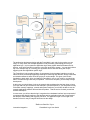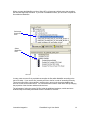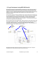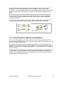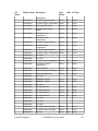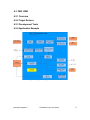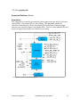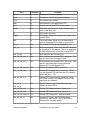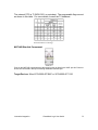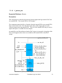
1
FrameWork Logic Users Guide
Innovative Integration
Copyright 2005. All rights reserved.
All information in this document is property of Innovative Integration and all rights are reserved.
This information is provided solely for the purpose of supporting use of Innovative Integration
products and software. No further license is granted or implied by this publication.
Revision
1.0
Changes
Initial release.
Author
Date
DPM
10/19/05
Table 1: Document Revision History
Innovative Integration
FrameWork Logic User Guide
1
1 Table of Contents
Table of Contents
1 Table of Contents.............................................................................................................2
2 List of Figures.................................................................................................................. 4
3 List of Tables.................................................................................................................. 6
4 Introduction......................................................................................................................7
4.1 Prerequisite Experience and Required Tools........................................................... 7
4.2 Organization of this Manual.....................................................................................8
4.3 Logic Component Naming Conventions..................................................................8
4.4 Where to Get Help....................................................................................................8
5 Logic Development Process.............................................................................................9
5.1 Developing Using VHDL.........................................................................................9
5.1.1 Using the FrameWork Library in VHDL.......................................................11
5.1.2 VHDL Simulation......................................................................................... 12
5.2 Logic Development using MATLAB Simulink..................................................... 19
5.2.1 Installation...................................................................................................... 20
5.2.2 MATLAB Simulink Use................................................................................ 22
5.2.3 Using Simulink in High Speed Applications..................................................23
5.3 Making the Physical Logic.....................................................................................25
5.3.1 Place and Route Reports.................................................................................26
5.4 Loading Logic ....................................................................................................... 27
5.4.1 JTAG.............................................................................................................. 27
5.4.2 Loading the Logic Using PROM Images........................................................31
5.4.2.1 Making the Device Image....................................................................... 31
5.4.2.2 Velocia Download.................................................................................. 38
5.5 Debugging.............................................................................................................. 39
5.5.1 Built-in Test Modes........................................................................................39
5.5.2 Xilinx ChipScope.......................................................................................... 40
5.5.2.1 Declaration Of ChipScope Core in VHDL............................................. 42
5.5.3 Debugging in MATLAB Simulink.................................................................45
6 FrameWork Designs...................................................................................................... 46
6.1 Quixote...................................................................................................................46
6.1.1 Overview........................................................................................................ 46
6.1.2 Target Devices................................................................................................46
6.1.3 Development Tools........................................................................................ 46
6.1.4 VHDL Application Logic Example................................................................47
6.1.4.1 Application Logic Help Files..................................................................48
6.1.4.2 Memory Map.......................................................................................... 48
6.1.4.3 Clocks..................................................................................................... 51
6.1.4.3.1 Clock Sources................................................................................. 52
6.1.4.3.2 Domains...............................................................................................53
6.1.4.4 A/D Interface.......................................................................................... 53
6.1.4.5 DAC Interface.........................................................................................54
Innovative Integration
FrameWork Logic User Guide
2
6.1.4.6 DSP Interface.......................................................................................... 55
6.1.4.6.1 DSP Bus EMIF A............................................................................55
6.1.4.6.2 DSP Bus EMIF B............................................................................ 59
6.1.4.7 Event Log................................................................................................59
6.1.5 MATLAB Simulink Logic Examples.............................................................59
6.1.6 Synthesis and Fitting ..................................................................................... 60
6.1.6.1 Getting Started........................................................................................ 60
6.1.6.2 Constraints.............................................................................................. 61
6.1.6.2.1 Timing Constraints.............................................................................. 61
6.1.6.2.2 Physical Constraints.............................................................................62
6.1.6.3 Logic Utilization..................................................................................... 63
6.1.7 Place and Route......................................................................................... 66
6.1.8 Simulation ..................................................................................................... 68
6.1.8.1 Using the Testbench................................................................................68
6.1.8.2 Simulation Models for Quixote.............................................................. 69
6.1.8.3 Simulation notes..................................................................................... 70
6.1.9 Making the logic image for downloading.......................................................70
6.1.9.1 Loading over PCI....................................................................................70
6.1.9.2 Loading over JTAG................................................................................ 70
6.1.10 Pitfalls, Gotchas and Tips........................................................................ 70
6.2 PMC UWB............................................................................................................ 71
6.2.1 Overview........................................................................................................ 71
6.2.2 Target Devices................................................................................................71
6.2.3 Development Tools........................................................................................ 71
6.2.4 Application Example...................................................................................... 71
7
Framework Library................................................................................................. 72
7.1 Hardware Components......................................................................................72
7.1.1 Quixote Hardware Components.................................................................... 72
7.1.1.1 ii_quixote_adc.........................................................................................73
7.1.1.2 ii_quixote_dac......................................................................................76
7.1.1.3 ii_quixote_dsp_emif_a........................................................................... 79
7.1.1.4 ii_quixote_dio......................................................................................... 83
7.1.1.5 ii_quixote_sbsram...................................................................................85
7.1.1.6 ii_quixote_dsp_emif_b........................................................................... 88
7.1.1.7 ii_quixote_clocks....................................................................................91
7.1.1.8 ii_quxiote_pmc_j4................................................................................. 93
8 Generic Components......................................................................................................95
8.1 ii_event_log............................................................................................................95
Innovative Integration
FrameWork Logic User Guide
3
2 List of Figures
Illustration Index
Illustration 1: VHDL Development Process...................................................................... 10
Illustration 2: Logic Architecture Showing Hardware and Application Layers.................11
Illustration 3: Compiling the Simulation Libraries............................................................ 13
Illustration 4: Setting Simulation Library Compilation Properties.................................... 13
Illustration 5: Invoking ModelSim from Xilinx ISE..........................................................14
Illustration 6: Configuring Xilinx ISE to use a custom DO file........................................ 15
Illustration 7: Loading the simulation in ModelSim..........................................................16
Illustration 8: Example ModelSim Workspace After Loading.......................................... 17
Illustration 9: ModelSim Wave Window Example............................................................18
Illustration 10: MATLAB Simulink Development ...........................................................19
Illustration 11: MATLAB Directory.................................................................................. 20
Illustration 12: Executing the MATLAB installation command........................................20
Illustration 13: Matlab Installation Directory Example..................................................... 21
Illustration 14: Simulink Product Library Example...........................................................21
Illustration 15: Building a Simulink Project...................................................................... 22
Illustration 16: Example use of MATLAB Gateways........................................................23
Illustration 17: Example of Real-time Signal Capture in MATLAB.................................24
Illustration 18: Example of Real-time Arbitrary Wave Generation in MATLAB............. 24
Illustration 19: Xilinx Implementation Tools.................................................................... 25
Illustration 20: Xilinx System Generator Implementation Control....................................26
Illustration 21: Getting Started with IMPACT.................................................................. 28
Illustration 22: Choosing the Operation Mode for IMPACT.............................................28
Illustration 23: Choosing the Boundary Scan Mode for IMPACT.................................... 29
Illustration 24: Automatic JTAG Chain Detection using IMPACT.................................. 29
Illustration 25: Selecting the Configuration Image Using IMPACT................................. 30
Illustration 26: Programming Devices using JTAG under IMPACT.................................31
Illustration 27: Using IMPACT to Make a PROM Image................................................. 32
Illustration 28: Selecting the PROM Operating Mode in IMPACT.................................. 32
Illustration 29: Selecting the Configuration Method in IMPACT..................................... 33
Illustration 30: Selecting the PROM size in IMPACT...................................................... 34
Illustration 31: Selecting the BIT file in IMPACT............................................................ 35
Illustration 32: Ready to Make the PROM Image in IMPACT......................................... 36
Illustration 33: Successful PROM Image Generation Using IMPACT............................. 36
Illustration 34: Velocia Logic and DSP Software Download Applet................................ 38
Illustration 35: Typical Debug Block Diagram..................................................................39
Illustration 36: Debugging with ChipScope.......................................................................40
Illustration 37: Xilinx Parallel IV Cable for Debug and Development............................. 41
Illustration 38: Xilinx Parallel Cable IV Target Cable...................................................... 41
Illustration 39: Xilinx Parallel Cable IV Pinout on IDC 5x2 2MM Header...................... 41
Innovative Integration
FrameWork Logic User Guide
4
Illustration 40: ChipScope Core Declarations................................................................... 43
Illustration 41: ChipScope Core Instantiation....................................................................44
Illustration 42: Xilinx ChipScope in Use...........................................................................45
Illustration 43: Quixote Logic and Peripherals.................................................................. 47
Illustration 44: Quixote Logic Block Diagram.................................................................. 48
Illustration 45: Quixote Logic Clock Domains..................................................................53
Illustration 46: Quixote A/D Interface and Application Logic.......................................... 54
Illustration 47: Quixote DAC Interface Block Diagram.................................................... 55
Illustration 48: TI DSP Asynchronous Memory Timing (Courtesy of Texas Instruments)...
56
Illustration 49: TI DSP Synchronous Memory Read Interface (Courtesy of Texas
Instruments)....................................................................................................................... 57
Illustration 50: TI DSP Synchronous Memory Write Interface (Courtesy of Texas
Instruments)....................................................................................................................... 57
Illustration 51: Quixote 6M Logic Utilization................................................................... 64
Illustration 52: Quixote 2M Logic Utilization................................................................... 65
Illustration 53: Quixote Area Constraint Logic Utilization............................................... 65
Illustration 54: Quixote Place and Route Report............................................................... 67
Illustration 55: Quixote Simulation Waveforms................................................................69
Illustration 56: PMC UWB Application Logic Block Diagram.........................................71
Illustration 57: ii_quixote_adc Block Diagram..................................................................73
Illustration 58Illustration 1Quixote ADC External FIFO Level Settings.......................... 75
Illustration 59: ii_quixote_dac Block Diagram..................................................................76
Illustration 60Quixote DAC External FIFO Level Settings...............................................78
Illustration 61: ii_quixote_emif_a Block Diagram............................................................ 80
Illustration 62: ii_quixote_emif_b Block Diagram............................................................88
Illustration 63: ii_quixote_clocks Block Diagram............................................................. 91
Illustration 64: ii_quixote_pmc_j4 Block Diagram........................................................... 93
Illustration 65: ii_event_log Block Diagram......................................................................96
Innovative Integration
FrameWork Logic User Guide
5
3 List of Tables
Index of Tables
Table 1: Document Revision History...................................................................................1
Table 2: Supported Logic Development Tools.................................................................... 7
Table 3: Logic Environments Pros and Cons.......................................................................9
Table 4: Xilinx Report Files Generated During Implemention......................................... 27
Table 5: Logic Development Tools for Quixote................................................................47
Table 6: Quixote Memory Map......................................................................................... 51
Table 7: Quixote Input Clocks...........................................................................................52
Table 8: MATLAB Examples for Quixote........................................................................ 60
Table 9: Quixote Xilinx ISE Project Filename.................................................................. 60
Table 10: Quixote Constraint Files.................................................................................... 61
Table 11: Quixote Simulation Models...............................................................................69
Table 12ii_quixote_adc Component Ports.........................................................................74
Table 13ii_quixote_dac Component Ports.........................................................................78
Table 14: DSP EMIF A use with ii_quixote_emif_a Component..................................... 79
Table 15: ii_quixote_emif_a Component Ports................................................................ 82
Table 16ii_quixote_dio Component Ports......................................................................... 84
Table 17: ii_quxiote_sbsram Component Ports.................................................................86
Table 18: ii_quixote_emif_b Component Ports.................................................................90
Table 19: ii_quixote_clocks Component Ports..................................................................92
Table 20: ii_quixote_pmc_j4 Component Ports................................................................ 94
Table 21: ii_event_log Alert Message Format...................................................................95
Table 22: ii_event_log Component Ports.......................................................................... 97
Innovative Integration
FrameWork Logic User Guide
6
4 Introduction
This manual is written to assist in the creation, implementation and testing of custom logic for
Innovative Integration products. The scope of this manual is limited to discussion of the logic
development tools, example logic designs and logic libraries provided in the Framework Logic
toolset.
Additional documentation on each product is provided for hardware features and software in other
manuals. These are used in conjunction with this manual for product development and use.
Thank you for using our products. Your comments and input are appreciated so that we can
improve our support and help you to be successful on your project. Email us at
[email protected] with your input or give us a call.
4.1 Prerequisite Experience and Required Tools
The designer is expected to have experience in VHDL to use the Framework Logic tools and
code. All components in the Framework Logic are VHDL source code whenever provided and
supported by VHDL models and test code. As a standard, the code is written in VHDL 1993
version which is widely used and supported.
The design tools used are listed here. We make an effort to keep the logic supported under the
newest versions, but in many cases the logic must be reworked and retested to support the
newest tool version. For each product, we have listed the required tool set that was used to
create the logic.
Here is the tools set list we use for supporting the Framework Logic use and development.
Function
Tool Vendor
Tool Name
Synthesis, Place and Route
Xilinx
ISE 7.1 or above
Simulation
Mentor Graphics ModelSim 6.1
Bit and PROM Image Creation
Xilinx
Impact 7.1
Signal Processing Design
MathWorks
MatLAB 7
Logic Design Under MATLab
Xilinx
System Generator 7.1
Logic Debug and Testing
Xilinx
ChipScope 7.1
Logic JTAG Cable
Xilinx
Parallel Cable IV or others
Table 2: Supported Logic Development Tools
The documentation for the development tools is provided by the tool vendor. All of them have online documentation and help that can acquaint you with their use. This manual makes no attempt
to replace them, but rather supplement them with specifics on using them with Framework Logic
application development.
While it is not expected that you are expert in these tools, these tools are used for Framework
Innovative Integration
FrameWork Logic User Guide
7
Logic development and are discussed in this manual. If you are using other tools, they should
have similar capabilities.
4.2 Organization of this Manual
This manual covers the main topics in using the Framework Logic for Innovative Integration
products for both HDL and MATLab Simulink development methods. The first few sections
describe the HDL tools and development methods including synthesis, placement and routing,
and simulation. For MATLab Simlink, the development process for logic is discussed using Xilinx
System Generator running the Xilinx ISE tools for synthesis, place and route. Finally, the
generating the logic image and debugging are discussed.
Each product supported by the logic is discussed, showing the details of the example logic are
shown. The hardware interface components and application logic internals are shown.
Finally, the Framework Logic library components are shown.
4.3 Logic Component Naming Conventions
For all hardware interface components, the standard naming convention is
ii_<product_name>_<function_name>
where <product_name> is the Innovative product this component is used on, and
<function_name> is a descriptor of the component. For example,
ii_quixote_dio
is the Quixote digital IO hardware interface component.
4.4 Where to Get Help
In addition to this manual, the example design for each product is provided with an HTML
document that allows designers to quickly navigate the design to understand the hierarchy,
entities used, ports and source code.
For help on Innovative Integration hardware or software, there are separate help manuals and an
on-line help system for the software tools. These manuals are provided on the CDs delivered with
the product or on the web at http://www.innovative-dsp.com/support/productdocs.htm . At this site,
you can download the product information, software and logic updates.
Help for other tools such as Xilinx or ModelSim is provided on-line with the tool. Xilinx also has an
excellent Answers Database on the web (http://www.xilinx.com/support/mysupport.htm) and
many examples of techniques used in FPGA design. This is the primary site for support on Xilinxspecific problems that can include tools problems and workarounds.
Technical support from Innovative Integration is available at
[email protected]
phone ++1 805-520-3300 Monday through Friday, 8 AM to 5 PM Pacific Standard Time
Innovative Integration
FrameWork Logic User Guide
8
5 Logic Development Process
The FrameWork Logic system supports two logic development methods: VHDL, or MATLab
Simulink, or a combination. Each system offers benefits and have strengths that in some cases
complement each other.
VHDL development is very flexible, allowing the developer the full freedom of a high level
language that is expressive and extensible. The FrameWork Logic system provides VHDL
components for hardware interfaces that allow the designer to quickly integrate custom VHDL
code into the application logic. Other library components are offered that provide some common
functions used in signal processing and control. Libraries from Xilinx and third parties are also
used to provide broad support for signal processing, analytical and communications applications.
Development
Tool
Pro
Con
VHDL
Expressive, extensible language. Gives
complete flexibility to the designer.
Design and debug of DSP algorithms
is more difficult and time consuming.
MATLAB
Simulink
Allows design of complex DSP algorithms Less capable of handling low-level
at a high level. Great visualization and
details. Less visibility and control of
analysis tools for design and debug.
logic design process.
VHDL +
MATLAB
Best of both tools gives optimum flexibility Multiple tools must be used resulting
where needed and high level design for
in a more complex development
complex DSP algorithms.
process.
Table 3: Logic Environments Pros and Cons
MATLAB Simulink offers a high-level block diagram approach to logic design that allows the
designer to work at a higher, more abstract level. Signal processing algorithms can be quickly
developed and simulated in MATLAB then directly ported to the logic hardware. Inside of the
FrameWork Logic tools, the designer can concentrate on the algorithms because the system has
a hardware interface layer that integrates the hardware with MATLAB cleanly and efficiently.
Application development is dramatically sped up for complex signal processing algorithms
because of the powerful capabilities within MATLAB for algorithm design, visualization and
analysis.
Many applications find that a mix of VHDL and MATLAB offer the best of both worlds: high level
signal processing development and the full flexibility of a high level language. It is common that
unique data handling, triggering and interface functions may be better expressed in VHDL, but
nothing beats the power of MATLAB for things like filter design, down-conversion and
mathematical analysis of data. The designer can mix VHDL components, or MATLAB-generated
components with one another in either environment and reap the benefits of each system.
5.1 Developing Using VHDL
Application logic development with the FrameWork Logic in VHDL follows the typical development
cycle: code creation, simulation, physical implementation and test. This flow is summarized in the
following diagram showing the Xilinx ISE tools and ModelSim as the primary development tools.
Innovative Integration
FrameWork Logic User Guide
9
Illustration 1: VHDL Development Process
The application development begins with the FrameWork Logic code for the product you are
using. In many cases, the example application code provides a good starting point for your
application logic. In most cases the application logic shows a basic data flow between the IO
devices, such as A/D and D/A converters, to the logic and DSP or system. You can then build on
top of the example logic by inserting your algorithms into the data flow along with unique
triggering and other application-specific logic.
The FrameWork Logic provides a library of components for the hardware interfaces as well as
others functions, an example application showing IO interfacing and data flow, design constraints,
a simulation testbench, and a Xilinx ISE project or each example. This gives you the basic
foundation to begin work. After you install the FrameWork Logic on your system, you should be
able to recreate the logic and verify its operation. Once that is complete, you are ready to begin
development.
At this point, you should have a look at the example logic and determine the best place to insert
your logic and how you can best use the example in your development. If you can preserve many
of the basic memory mappings, controls and system interfaces, you will then be able to use the
example application software delivered with the product. That saves time for both you and the
software developers.
In most cases, you will see that the logic is organized as a hardware interface layer composed of
components that directly interface to the hardware and an application layer that is composed of
the analysis, data handling and triggering functions. The application layer is on a single clock
domain so that it is easy to integrate functions into the design.
Hardware Interface Layer
Innovative Integration
FrameWork Logic User Guide
10
Illustration 2: Logic Architecture Showing Hardware and Application Layers
Hardware Interface Layer
HW
Interface
Application
Layer
(your logic does here)
HW
Interface
Code for your application layer design can be created in a number of ways: written in VHDL or
Verilog, created in MATLAB, or included as a black box netlist from a third party such as Xilinx or
others. If you design you logic to run on a single clock it is then easier to integrate into the
application layer of the FrameWork Logic. This is usually possible because the other clocks in the
design, such as the A/D sample clocks, or hardware-specific clocks are handled in the hardware
interface layer. The use of a single clock in the application layer allows the designer to use the
timing and physical constraints associated with the hardware interface components.
5.1.1 Using the FrameWork Library in VHDL
The components in the FrameWork Logic library are divided into generic components that may be
used in any design, and hardware-specific components.
The hardware-specific components are used in the designs for A/Ds, DACs, memories and the
like that have unique interface protocols and timings. Constraints in the specific design for IO
standards and specific timing requirements are usually required for use. The constraints for the
hardware-specific components are found in the application example that includes that component.
All hardware-specific components have unique names such as ii_quixote_adc. The naming
convention prevents inadvertent naming collisions with your design if you do not use a ii_ prefix on
your components. The hardware name is included in the name showing which design uses this
component.
In the installation, you will find that hardware-specific components in the directory for that specifc
design. The generic components are in the ii_library directory. To use the compoents, you can
copy them into the design you are creating, or reference the library directory.
Also, you may need to include packages supporting the components in your design. For example,
ii_quixote_dsp_emif_a component requires ii_pkg to be included. This is done by including these
statements in the component and by compiling the package in your design.
library work;
use work.ii_pkg.ALL;
One problem that frequently occurs is that the simulation requires the package be compiled for
use. The script that Xilinx ISE produces seems to exclude these packages for compilation, so be
sure to compile the required packages separately.
Innovative Integration
FrameWork Logic User Guide
11
5.1.2 VHDL Simulation
Simulation is an important part of the logic development process. All designs that are targeted at
using the large logic devices supported by the Framework Logic require simulation for successful
implementation. If you do not simulate your design, it is unlikely that you will successfully complete
it during your lifetime.
For simulation, we are currently supporting ModelSim 6.1 PE. The Xilinx MXE version cannot be
used since it cannot be used simulate designs as large as the FrameWork Logic designs.
The Framework Logic includes a test bench and models required for most simulations. In many
cases the models are simple representations of the device that give a data pattern that is easy to
follow through the simulations. More complex waveforms can always be substituted later for
proving out the signal processing or data analysis portions of the design. In each design, the list
of files shows the applicable test bench name and available models.
The testbench contains a set of simulation steps that exercise various functions on the framework
logic for basic interface testing. Behavioral procedures have been written to simulate the DSP
timing for sync and asynchronous memory accesses that are useful in simulating data movement.
Also, the steps to setup the logic for data streaming support are shown so that interrupt servicing
(DMA or CPU accesses), trigger and event log use are illustrated.
As delivered, the FrameWork Logic example provides a basic example in the use of the hardware
interface components, data flow through the design, and some simple triggering control. It is
anticipated that you can use this example test bench as a starting point for your application logic
simulation. Your logic can be added to the simulation in many cases without modifying the test
bench since the application logic does not change the external pins on the design.
Before simulation can begin, the pertinent libraries must be compiled for the chip you are
targeting. If you are starting from Xilinx ISE, this is done by selecting the device in the Sources
window, then double-clicking the “Compile HDL Simulation Libraries” process in the Processes
window. This will compile the unisim, simprim and xilixcorelib files necessary for simulation. You
may have to configure this process so that it points at your current ModelSim installation; this is
done by right-clicking and setting the parameters. If you are working with ModelSim standalone,
be sure to compile the libraries unisim, simprim and xilinxcorelib and add them to the libraries in
ModelSim (vlib) before attempting to simulate.
Innovative Integration
FrameWork Logic User Guide
12
Selecting
the device
Compiling
the libraries
Illustration 3: Compiling the Simulation Libraries
Illustration 4: Setting Simulation Library Compilation Properties
Simulation can be started in either the Xilinx ISE environment, or by using the ModelSim tool in a
standalone mode. In Xilinx ISE, select the test bench file in the Sources in Project window. This
then will show the simulations that can be run in the Processes window using ModelSim. Usually,
the functional simulation is best to use when you are creating code because the simulation will
execute quickly. Once you have the right functionality, you can then use the timing simulation to
verify performance at speed.
Innovative Integration
FrameWork Logic User Guide
13
When you enter the ModelSim tool from Xilinx ISE, it will execute a default macro that compiles
the files and begins the simulation. If you enter in standalone mode, you will need to compile the
files within the ModelSim.
Select test
bench file
here
Select
ModelSim
here
Illustration 5: Invoking ModelSim from Xilinx ISE
In many cases a macro file is provided that compiles the files within ModelSim according to the
macro file order. If you use this file, just add your files to the list in order of ascending hierarchy.
These macro files have a .do extension; usually project_name.do for the project loading, and
wave.do for the wave window format. You can reference this macro inside Xilinx ISE by changing
the properties of the simulator window as shown here.
The advantage of using the custom DO file is that the additional packages, models and wave
window setup can be easily automated when the simulator is invoked.
Innovative Integration
FrameWork Logic User Guide
14
Illustration 6: Configuring Xilinx ISE to use a custom DO file
Innovative Integration
FrameWork Logic User Guide
15
Illustration 7: Loading the simulation in ModelSim
When the design is loading, you will see each components loaded in the transaction window as
shown here. If anything fails to load, check that its ports match those in the instance where it was
used.
Innovative Integration
FrameWork Logic User Guide
16
Illustration 8: Example ModelSim Workspace After Loading
Once the design is loaded, the design hierarchy is shown in the Workspace window with the test
bench at the top of the hierarchy. Here is an example.
Innovative Integration
FrameWork Logic User Guide
17
Illustration 9: ModelSim Wave Window Example
Once you are inside the ModelSim environment, you should be able to use the tools to run
simulations of the design. The wave window is many times the main focus since it gives a logic
analyzer view of the design.
You can quickly view debug the design within ModelSim because you can probe the logic down to
the lowest level. This visibility is often lost after synthesis and fitting because logic is minimized by
the tools and may be trimmed out if unused, even if by accident. When you select an design unit
within ModelSim Work Space window, the processes, signals and variable for that design unit are
shown. You can add them to the window by selecting them and right-clicking to add to the wave
window.
Some common simulation problems are
•
libraries are wrong version – be sure to compile them from within Xilinx ISE before use
•
wrong simulator resolution – be sure to use 1 ps resolution for all designs
•
design won't load – be sure all models and packages were compiled
•
naming conflicts – all instances must have a unique name
•
source code won't compile – check that you compile with the correct version for 1993 to
2000 version of HDL
Innovative Integration
FrameWork Logic User Guide
18
5.2 Logic Development using MATLAB Simulink
MATLab Simulink provides a powerful method of developing logic using a high level design tool
that integrates hardware into the MATLAB Simulink environment. Complex signal processing
designs can be developed rapidly using the Simulink block diagrams interacting with the actual
hardware in real time. Gateways between MATLAB Simulink and the hardware allow data to flow
between the actual hardware and MATLAB, bringing the power of MATLAB to the logic
development process.
Simulink blocks diagrams are directly translated into logic using the Xilinx System Generator tool.
For each supported product, a hardware interface layer of Simulink components is provided that
allows the hardware to be used in the the Simulink design.. Simulink components from the
various libraries provided by Mathworks, Xilinx and Innovative interface with this hardware
interface layer for building the application logic on the product. The Xilinx place and route tools
are used for the logic build as in any HDL project.
Here is a typical Simulink block diagram design. Notice the Xilinx icon in the upper left; this is the
Xilinx System Generator control block. This block provides the link to the Xilinx place and route
tools used to implement the logic. The other blocks are mixture of hardware interface
components, such as the Quixote A/D converters, SRAM and DACs. The remaining blocks are
Simulink functions for control, display and data formating.
Xilinx
System
Hardware
Generator
Interface blocks
Block
Illustration 10: MATLAB Simulink Development
MATLAB Simulink library components are shown in the library for each product. Examples
illustrating the use of MATLAB are provided in each product section.
Innovative Integration
FrameWork Logic User Guide
19
5.2.1 Installation
You must have installed MATLAB Simulink prior to installing the product MATLAB
support.
The co-simulation library is provided as a zip file and a Matlab installation script.
setup_<<product_name>>.zip
Unzip the software, preserving the directory structure.
The next step is to start Matlab and point at the installation directory In this directory, you will find
a Matlab installation script, <<product_name>>_compilation.m . This script installs the product
Simulink library into the MATLAB environment. The script assumes that the MATLAB installation
directory is c:\matlab7. It is easiest if your MATLAB installation is in this directory. If not, you can
rename the MATLAB installation directory or you will have to change the installation .m file, and
the library .mdl files to the installation directory name.
To do this compilation and installation, follow these steps:
1. Open Matlab and point at the installation directory.
Illustration 11: MATLAB Directory
2. Change the directory to the folder containing <<product_name>>.zip and
setup_<<product_name>>_compilation.m file.
Illustration 12: Executing the MATLAB installation command
3. IN the MATLAB command window, enter <<product_name>>_ compilation on the Matlab
command prompt. This command should unzip the library files and install the product
library. This command could take several minutes to execute.
Innovative Integration
FrameWork Logic User Guide
20
Illustration 13: Matlab Installation Directory Example
4. Quit MATLAB and restart..
Now the product library should be visible in the Simulink Library Browser window.
Illustration 14: Simulink Product Library Example
The library is now ready for use in MATLAB.
The files controlling the compilation process are in the
C:\MATLAB7\toolbox\sysgen\jtagcosim\product_name directory.
Innovative Integration
FrameWork Logic User Guide
21
5.2.2 MATLAB Simulink Use
In MATLAB, you can make new block diagrams for logic designs using the libraries for Xilinx and
the specific product. Creating a new logic diagram is often aided by starting with one of the
examples for the product you are using as a starting point. You can then drag and drop Simulink
blocks into the worksheet to build the logic functionality you need.
The two ways to use the Simulink environment are to generate an entire logic design, using the
hardware layer provided by Innovative, or to make logic components that are incorporated into
your VHDL design. When building an entire logic design, you are using the hardware interface
layer as given in the top level of the application logic found in the
C:\MATLAB7\toolbox\sysgen\jtagcosim\Innovative_product_name directory. You
can also see the underlying VHDL for the components in the library in this directory. They are
used during the compilation process by Xilinx System Generator.
When you are using the environment to generate a logic block used in a VHDL design, it may well
be independent of any specific hardware design. The Simulink blocks used in these designs will
essentially be linked together and compiled, resulting an .NGC netlist file that is linked into the top
level VHDL design. Keep in mind that this is a black box approach and the resulting block can be
simulated only at the component level by using NETGEN to create VHDL for the simulation. The
VHDL from NETGEN will be hard to understand, so the debug of the block should be done in
MATLAB prior to use.
You are always required to include the Xilinx System Generator logic block to provide the link to
the Xilinx tools. This is shown in the following diagram. Through this block, you can control the
compilation and fitting process for the logic design. All options normally available for the Xilinx
PAR tools are made available through this block.
Illustration 15: Building a Simulink Project
Innovative Integration
FrameWork Logic User Guide
22
An important feature in the Simulink environment is the ability to use Simulink for active cosimulation. This means that real hardware can be accessed from within in the Simulink
environment. You can generate test signals, run them through the logic device on you card and
then observe the output. This allows you develop on the real hardware for design, test and
debug.
Gateways are used to provide the link between the Simulink environment and the hardware.
These gateways allow you to use the power of MATLAB Simulink for complex mathematical
functions required for signal generation on complex systems and the powerful visualization
capabilities in MATLAB.
In the first example, gateways are used to input a signal from MATLAB into the hardware. The
second example shows a gateway used to display data in MATLAB from the hardware.
Illustration 16: Example use of MATLAB Gateways
5.2.3 Using Simulink in High Speed Applications
Data rate over the gateways is limited to the data rate of the JTAG connection to the FPGA ,
which is only about 4 Mb/s typically. Even if you buy the fastest cable, it is only 20 Mb/s – too slow
to look at high speed, real-time data.
A technique used to improve interaction with high speed systems is to use the SRAM on the
hardware as a data buffer for capture or signal generation. The SRAM can then interact with the
hardware at full speed and take snapshots of the data for viewing or play data into the system at
full rate for testing.
For data capture, the SRAM contents are read back into the MATLAB environment and displayed
or analyzed much like an oscilloscope or spectrum analyzer would operate. In the following
example, data is captured from the A/D into an SRAM and can then be read back into Simulink
using a gateway for viewing and analysis.
Innovative Integration
FrameWork Logic User Guide
23
SRAM used
for data
capture or
playback
Illustration 17: Example of Real-time Signal Capture in MATLAB
To get signals from MATLAB into the hardware, the SRAM can be used as an arbitrary waveform
generator when it is loaded with a test waveform that is then played out real-time. MATLAB is
ideal for generation of the complex waveforms found in communications applications. In the
following example, the SRAM is loaded from a Simulink gateway with a waveform, then is played
out of the SRAM at high speed to a DAC.
Illustration 18: Example of Real-time Arbitrary Wave Generation in MATLAB
Innovative Integration
FrameWork Logic User Guide
24
5.3 Making the Physical Logic
After the logic has been created, either with HDL or MATLAB, it must be implemented in the logic
through a process of placing and routing the logic into the physical device. For either
development process, the physical design is done using the Xilinx tools. These tools take the
netlist created by the synthesis process or Xilinx System Generator and map it into the physical
device while meeting timing and physical constraints.
Each design has a unique set of constraints for timing and physical placement that describes the
requirements of the logic. This file is the UCF (User Constraint File) used by the design. This
UCF file is provided for each FrameWork Logic design, though it may need to be modified in
some cases for your application logic.
The Xilinx ISE tools are used for the physical logic creation. For HDL designs, these tools are
accessed through the ISE environment in the processes window as shown here. The main steps
are translate (link), map and place & route.
Illustration 19: Xilinx Implementation Tools
There a many options for each of the implementation steps which are set in the individual project
files for each FrameWork Logic example.
Since most of the chips on the products are very large, we have chosen to preserve the hierarchy
of the design during the implementation so that area constraints and incremental design approach
may be used. Area constraints allow the designer to control the placement of logic on the FPGA
chip for best timing control. With area constraints, the logic will be constrained to where you put it
and in many cases helps the tool do a better job overall.
We also recommend that you use the incremental design approach in the logic implementation
process when working with the large FPGA designs. This allows you to make minor changes to a
chip during debug and test without requiring the tool to reroute the whole design. In this way,
functions that are not affected by the change are not touched so their behavior and timing does
not change.
For MATLAB Simulink, the Xilinx System Generator icon is used to control the implementation
Innovative Integration
FrameWork Logic User Guide
25
process. Double-clicking the icon allows you to configure the Xilinx ISE tools that are used for the
logic build just as you would for an HDL design. The implementation settings are set in the
window as shown here.
Illustration 20: Xilinx System Generator Implementation Control
5.3.1 Place and Route Reports
The place and route implementation by the Xilinx tools results in several files you may want to
review in case of problems.
Innovative Integration
FrameWork Logic User Guide
26
File
extension
Contents
What to Look For
.BLD
The output from the NGDBuild
process that link all the logic
together
There should be no errors. This program issues
numerous warnings but there should be no
errors. Most link errors occur because of missing
netlist files – Coregen put the files somewhere
else, or a missing netlist from a black box.
.MAP
The output from the MAP process
that does the logic mapping to the
physical device. Removes
unused logic and.
There should be no errors, but warnings are
usually OK. Common problems range from
incompatible logic mappings, impossible area
constraints, and clock connections.
.PAR
The output of the Place and
Route implementation process.
Shows timing results and fit
results.
Timing constraints should be met. Review the
summary at the end of this report to see if timing
is OK since it will complete no matter how bad it
is. Also look for any incomplete routing.
.BGN
The output of the Bitgen tool.
Normally, this is not a problem. Occasionally
though the design will route but not complete
Bitgen will report this error.
Table 4: Xilinx Report Files Generated During Implemention
In many designs, you will have to resolve timing problems that are shown in the place and route
process. Xilinx has several tools to help find the problems; Timing Analyzer is usually the place to
start. This tool helps you to understand the reason the logic did not meet timing – too many
connections, bad routing, etc. The tool suggests how to fix it. This is usually helpful but may
mean you are back to functional simulation again to add pipelining or change the logic and must
re-implement the design.
Once you achieve one good result, you may want to switch to incremental mode in the tool. This
allows you to use the last good result for most of the design that is unchanged when minor fixes
are made. For big changes however, you will need to reroute the whole chip.
Expect that the implementation process will be in the range of ½ to 2 hours in length depending
on your computer, how easy it is to meet constraints and how big the chip is. A tightly packed,
fast big chip will take a while. A VP40 that is 85% full, running at 130 MHz takes about 1.5 hours
to route on a Pentium 4 with 1 GB of RAM.
The final output of the implementation process is a .BIT file that represents the logic image. This
file is used to create a ROM image or for direct JTAG downloading.
5.4 Loading Logic
There are usually two methods of loading logic into the target FPGA : JTAG and from a PROM
image. JTAG is normally used during the development process because it is quick and easy to to
use. The ROM image is normally used after logic development is complete and the application is
deployed.
5.4.1 JTAG
Logic images may be loaded using the JTAG interface to the FPGA using a Xilinx JTAG cable
such as Parallel Cable IV or others. This provides a convenient method of quickly loading the
logic during the development process but is not usually used in deployed applications.
Innovative Integration
FrameWork Logic User Guide
27
The Xilinx IMPACT application is used to load the logic into the application FPGA. The IMPACT
tool may be invoked from the Xilinx ISE tool or as a standalone application.
When you enter the tool, you will be prompted for either a stored project or to create a new one.
The first time you use this, you should create a new project. Later, you can save the project and it
remembers the scan chain and files for the project.
Illustration 21: Getting Started with IMPACT
After you select create a new project, the IMPACT wizard will direct you through the process of
identifying the JTAG scan chain, assigning files and programming the devices. The first step is to
select Operation Mode. For JTAG, pick configure devices.
Illustration 22: Choosing the Operation Mode for IMPACT
Innovative Integration
FrameWork Logic User Guide
28
The next screen will prompt for what type of configuration to perform. Choose the Boundary Scan
Mode as shown.
Illustration 23: Choosing the Boundary Scan Mode for IMPACT
Next, IMPACT will prompt for the JTAG chain identification. Choose the automatic identify mode.
Illustration 24: Automatic JTAG Chain Detection using IMPACT
Innovative Integration
FrameWork Logic User Guide
29
If all goes well, IMPACT will find all the devices in the JTAG chain and display them as shown in
this example. If not, check the cable connection to the board. The cable should be detected by
IMPACT; if not, check that the port it is connected to on the PC is working and in the proper
mode. If the chip is not detected, be sure you have the right scan path, that the board is powered
up normally, and that IMPACT was able to connect to the scan path. Power everything off and try
again if it fails and you don't see any obvious problems. You can also check your setup and
software on a good card if you have one. If you don't, curse some then call tech support.
The next step is to assign a bit file to each device to be programmed. Right click each device and
use the dialog to assign the BIT file for programming each device. Double-check that you are
using the correct BIT file – you could damage the chip if it gets the wrong logic.
Illustration 25: Selecting the Configuration Image Using IMPACT
The last step is to program the device. This is done by right clicking the device and selecting
PROGRAM. This will only program the device you are selecting at that time. If it succeeds, then
you will be notified by IMPACT as shown in the example screen.
NOTE: We have found problems using the VERIFY function. It seems as though IMPACT has
some problems doing this and will usually fail. It is our experience however that if the
programming succeeds, then you will be OK. Xilinx employs a rigorous checksum routine that is
very good and seems to guarantee that programming succeeded when it reports as such. Let's
all hope they have this fixed sometime for our collective peace of mind.
Innovative Integration
FrameWork Logic User Guide
30
Illustration 26: Programming Devices using JTAG under IMPACT
5.4.2 Loading the Logic Using PROM Images
5.4.2.1 Making the Device Image
For all Innovative products, an EXORMacs format (.EXO) text file must be generated from the
output .BIT file produced by the place and route process. This is done by opening the Xilinx
IMPACT tool that is a PROM File Formatter utility from within the ISE and converting the BIT file
into an EXO file.
When you enter the tool, you will be prompted for either a stored project or to create a new one.
The first time you use this, you should create a new project. Later, you can save the project and it
remembers the PROM settings and files for the project.
Innovative Integration
FrameWork Logic User Guide
31
Illustration 27: Using IMPACT to Make a PROM Image
The next screen will prompt you to either configure devices or make a configuration file. To make
a PROM image, select Prepare Configuration Files.
Illustration 28: Selecting the PROM Operating Mode in IMPACT
Innovative Integration
FrameWork Logic User Guide
32
For a generic PROM file, used for most Innovative products, on the next screen you should select
PROM file for the image type.
Illustration 29: Selecting the Configuration Method in IMPACT
The PROM properties must be set to “bytewide” and EXORmacs to generate the required EXO
file. Once the properties are set, the .EXO file is generated in the source directory. Please refer to
the picture below:
Innovative Integration
FrameWork Logic User Guide
33
Illustration 30: Selecting the PROM size in IMPACT
In PROM Configuration screen, select the following options:
• Select Parallel PROM.
• Select EXO as File Format.
• Memory Fill Value - 0xFF
then provide a File Name.
Innovative Integration
FrameWork Logic User Guide
34
Illustration 31: Selecting the BIT file in IMPACT
You will then be prompted before the file is made – you last chance to not overwrite you last
PROM if you did not change the name or file path.
Innovative Integration
FrameWork Logic User Guide
35
Illustration 32: Ready to Make the PROM Image in IMPACT
The final screen will report successful operation.
Illustration 33: Successful PROM Image Generation Using IMPACT
Innovative Integration
FrameWork Logic User Guide
36
You are now ready to load the PROM image using one of the tools provided by Innovative or by
your application. Each family of cards has a specific logic programming utility and software
support. Here is a list of the tools for the card families.
Innovative Integration
FrameWork Logic User Guide
37
5.4.2.2 Velocia Download
The Velocia family of products, including Quixote and Quadia, use a simple Windows application
to download logic images to the card. The same application can be used to load DSP files, see
the software documentation for information.
Note: The application logic must be loaded after each power-up since there is no on-card
logic ROM.
The logic is loaded over the SelectMAP interface to the FPGA via the PCI bus. The logic may be
loaded and reloaded at any time during operation.
The Velocia Download applet requires a logic image in EXO format. To create this file, see the
previous section of this manual.
To load the logic image, press the button that looks like an electrical plug. You will be prompted
for a file name to load. Status indicators will first show the logic file being parsed, then the
loading. Loading takes about 20 seconds for a 6M device.
Load DSP
COFF
Which DSP
card you are
loading
Load
Logic
Image
The logic
image loaded
Boot the
DSP
Illustration 34: Velocia Logic and DSP Software Download Applet
The Velocia Download applet shows the logic filename that was loaded in he lower right corner.
Multiple cards in a single system are supported via the target number box. You can identify which
card is which target by blinking its LED with the VelociaFinder applet. The type of card is selected
in the drop-down box.
Software tools for loading the logic from application software are provided for loading the logic
Innovative Integration
FrameWork Logic User Guide
38
also. These are detailed in the software manual.
5.5 Debugging
It is inevitable that the logic will require some debugging and it is best to have a strategy for debug
before you actually use the hardware. Debugging on actual hardware is difficult because you have
poor visibility into the FPGA internals.
For HDL designs, the best and easiest debug method is simulation for functional and timing
problems. This gives the best visibility and interactivity to debug problems before the real
hardware is tested. A good set of test cases that stress the design should be run prior to working
on the real hardware. You will save time in the overall design process by doing a thorough job in
simulation. Sermon over.
There are several techniques that have worked for us on projects: Xilinx ChipScope, built-in test
modes, and judicious use of test points. Between these techniques and the capabilities of each
method, it is usually possible to find and fix bugs that are either functional design errors or timing
problems.
MATLAB Simulink developers can use the “hardware in the loop” features of system to debug the
design at a high level. Simulink can be used to generate test data or for viewing and analyzing
real hardware data. This is invaluable in debugging complex signal processing designs.
Here we will discuss a few of these techniques.
5.5.1 Built-in Test Modes
Another good way to debug your design is to have built-in test modes in the logic. If you plan
ahead for test, then you can more quickly validate your design later and spot problems. When you
finish the design, if the test generators and checkers can be left in the design, they are there later
as production debug or test.
In many designs, test pattern or data generators are invaluable since they provide known data into
the FPGA so that the output is known. If the data source is analog in the real design, substituting
perfect data is nice because it helps spot problems that may be hidden in the noise. The test
pattern may be an easily recognized stream, like incrementing numbers, that are easy to check in
the logic or on the test equipment. Also, its easier to test the extreme cases of the design that
may be difficult to reproduce with real signals.
Illustration 35: Typical Debug Block Diagram
Innovative Integration
FrameWork Logic User Guide
39
Another built-in test method is to use data checkers in the logic sprinkled through the data chain
help to spot the source of problems. If you have a missing timing constraint or a clock domain
issue, these can be hard to catch since they may be rare. A data checker gives you a way to look
for bad data and then trigger ChipScope or the logic analyzer. In many cases, rare errors are
impossible to catch without this sort of data checker. This technique has saved time because the
trigger at the bad data point allows you to inspect all the suspect signals and find the culprit.
5.5.2
Xilinx ChipScope
Xilinx offers an excellent tool for debugging FPGA designs call ChipScope. This tool works over
the FPGA JTAG port using any of the standard Xilinx JTAG cables. Software on the PC connects
to a ChipScope logic core that you embed in your logic. This is an optional tool from Xilinx and is
not included in the standard ISE software. For its cost of under $1500, we have found it well worth
the money.
Illustration 36: Debugging with ChipScope
The ChipScope core allows you to monitor internal FPGA signals using triggers and a sample
clock. The number of signals you can monitor and use for triggers is set up when you generate
the ChipScope core. The core size is determined by the number of signals monitored and the
number of samples stored. If the core gets too big, it will affect your design and tends to muddle
the debug process. Sometimes it is better to have a small core that has a small footprint and
does not interfere with the other logic for this reason.
The clock is used as the sample clock for the logic so it should be synchronous to the inputs
signals or sufficiently fast to sample them accurately. The size of the core
You will interact with the ChipScope software over a JTAG cable to the target device. This link is
limited to about 4-20 Mb/s, so it is not really real-time, but rather just a means to get the data from
the FPGA to the ChipScope software. The signals are captured in the FPGA block RAMs so the
record length is somewhat short being limited in most cases to 256 to 1K points.
Because of these limitations in JTAG speed and capture size, it is important to devise triggering
methods that allow you to catch the error condition. It is common to devise a piece of error
detection logic that serves as a trigger to ChipScope to best use the capture RAM. It is possible
Innovative Integration
FrameWork Logic User Guide
40
to pre-trigger or post-trigger in the software which makes trigger design easier.
Here is one of the common cables used for debug, just for reference.
Illustration 37: Xilinx Parallel IV Cable for Debug and Development
Illustration 38: Xilinx Parallel Cable IV Target Cable
Illustration 39: Xilinx Parallel Cable IV Pinout on IDC 5x2 2MM
Header
CAUTION:
The user MUST make sure that Xilinx JTAG cable connector is plugged in the proper
polarity to the Innovative target connector. If by mistake, the user connects the Xilinx
cable incorrectly, this may damage the target card and Xilinx POD. See the hardware
manual for each product to locate the connector and its pinout.
Innovative Integration
FrameWork Logic User Guide
41
5.5.2.1 Declaration Of ChipScope Core in VHDL
The ChipScope core is simple to use. Just connect up the signal for observation to the data ports,
the trigger signals to trigger and the clock. The number of ports and triggers is defined when you
create the debug core in the ChipScope tool. The clock is used as the sample clock for the logic
analyzer, so you must use a clock that is higher frequency than the signals you wish to observe.
Here’s a core we used in debug shown below.
Innovative Integration
FrameWork Logic User Guide
42
---
ICON core component declaration
-------------------------------------------------------------------component icon
port
(
control0
:
out std_logic_vector(35 downto 0)
);
end component;
---------------------------------------------------------------------
ICON core signal declarations
-------------------------------------------------------------------signal control0
: std_logic_vector(35 downto 0);
----------------------------------------------------------------------------------------------------------------------------------------
ILA core component declaration
-------------------------------------------------------------------component ila
port
(
control
: in
std_logic_vector(35 downto 0);
clk
: in
std_logic;
data
: in
std_logic_vector(77 downto 0);
trig0
: in
std_logic_vector(2 downto 0)
);
end component;
Illustration 40: ChipScope Core Declarations
Here is its instantiation during a debug session.
Innovative Integration
FrameWork Logic User Guide
43
---------------------------------------------------------------------
ICON core instance
-------------------------------------------------------------------i_icon : icon
port map
(
control0
=> control0
);
---------------------------------------------------------------------
ILA core instance
-------------------------------------------------------------------i_ila : ila
port map
(
control
=> control,
clk
=> clk,
data
=> data,
trig0
=> trig0
);
control <= control0;
trig0(0) <= sw_trigger(2)or sw_trigger(3);
trig0(1) <= ace_n(1);
trig0(2) <= ace_n(0) ;
clk <= dsp_Aeclk;
data(7 downto 0) <= dsp_a_ififo_wr_count(0);
data(14) <= dac_run;
data(13) <= dsp_a_ififo_wr(0);
data(12) <= adc_fifo_wen_n_s;
data(11) <= adc_int_raw;
data(43) <= dac0_ae_n;
Illustration 41: ChipScope Core Instantiation
Innovative Integration
FrameWork Logic User Guide
44
In this case, the designer was using the DSP EMIF A clock as the ChipScope core clock and had
several triggers including DSP memory decodes and software triggers. Some of the signals being
observed are shown as well such as FIFO read enables and so forth. Looks like the debug was
for some type of DSP access problem.
Once the core is in the design, you can then trigger on different conditions just as you would use a
logic analyzer. If connect up all the signals in the problem area, only one compilation is needed to
get the core into the design for debug. Once you get it all working, you have a logic analyzer
inside the FPGA. Here’s sample view.
Illustration 42: Xilinx ChipScope in Use
5.5.3 Debugging in MATLAB Simulink
The most common way to debug a MATLAB design is to use the hardware gateways to get data
between the design environment and the hardware. By adding a few observation points, you can
usually spot the problem area for most problems. You can also inject test waveforms into the
system to help find the problems.
Since MATLAB designs are normally implemented with a single system clock that all application
logic uses, timing problems tend to be minimized. Its a lot more common in MATLAB designs to
have data format problems. Keep in mind that MATLAB works in double precision, so you will
have to use data formatters frequently to get the data you expect in the real hardware. The design
is bit-true and cycle-true as implemented, but using it with MATLAB can be tricky to get the data
formats correct.
One of the most common method we use to find problems in the real hardware is to use an
SRAM for data capture of the real-time data, or to generate real-time data into the system.
Several of the examples show this technique. This technique allows you to capture real-time data
then analyze it in MATLAB. You can also build a logic analyzer this way by recording the states
into the RAM based on a trigger in the logic. See the sram_sinewave_fast_access_test example
in Quixote for a sample of this or a similar one for the hardware you are using.
ChipScope tends to be less useful in MATLAB debugging since the net names are not known and
can be hard to trace.
Innovative Integration
FrameWork Logic User Guide
45
6 FrameWork Designs
6.1 Quixote
6.1.1 Overview
The Quixote has two FPGAs on it : a Xilinx Spartan2 (200K gates) and a Xilinx Virtex2 (2M or 6M
gates). The Virtex2 is used for the analog interfacing and as the computational logic on the board.
Major elements inside the Spartan2 logic are the PCI interface, interrupt control, timebase
selection and message mailboxes. The Spartan2 source code is not normally provided.
Quixote II and III are open logic products that include additional memory for FPGA computational
space, and either a 2M (II) or 6M (III) gate Xilinx Virtex2 FPGA. The logic in Quixote I is provided
in source form to assist in custom application developments.
Quixote supports in-circuit reconfiguration of the Xilinx Virtex2 over its Select Map interface.
FPGA logic images may be downloaded to the Virtex2 logic as part of the software application at
any time of its SelectMap interface. The Pismo toolset provides software support for logic
configuration (see the VelociaDownload.exe applet and the ArmadaMatador.hlp/chm help file
under TIIVelocia).
6.1.2 Target Devices
Quixote has as its user programmable logic a Xilinx Virtex2 FPGA. The Virtex2 FPGAs have
many resources in addition to the logic gates such as embedded RAM blocks, digital clock
managers (DCMs), and flexible IO standards that are used in the sample logic. The Quixote is
offered with either a 2M gate device or 6M gate device.
Quixote Variant
Logic Density
Device Used
Quixote II (80069-2)
2M
Xilinx XC2V2000-4FF896C
Quixote III (80069-3)
6M
Xilinx XC2V6000-4FF1152C
Note : Quixote I (80069-1) does not support user programming of the logic.
6.1.3 Development Tools
The currently supported tool set is shown here.
Innovative Integration
FrameWork Logic User Guide
46
Function
Tool Vendor
Tool Name
Synthesis, Place and Route
Xilinx
ISE 7.1 or above
Simulation
Mentor Graphics
ModelSim 6.1
Bit and PROM Image Creation
Xilinx
Impact 7.1
Signal Processing Design
MathWorks
MatLAB 14 sp1
Logic Design Under MATLab
Xilinx
System Generator 7.1
Logic Debug and Testing
Xilinx
ChipScope 7.1
Logic JTAG Cable
Xilinx
Parallel Cable IV or others
Table 5: Logic Development Tools for Quixote
6.1.4 VHDL Application Logic Example
As a starting point, here is a big overview of what is attached to the Virtex 2 FPGA. All of the high
speed data interfaces have 32K sample FIFOs for buffering the data to the Virtex2 logic. The DSP
has both buses attached to the logic, and also two of the McBSP ports so that ample data
movement is supported.
Illustration 43: Quixote Logic and Peripherals
The logic design is organized as a hardware interface layer, which provide the direct interface to
the external peripherals, and the application logic components that do specific functions for signal
processing and control. Hardware interface components in the design include the A/D interface
components, ii_quixote_adc, for example and the A/D interface, ad_interface, providing specific
triggering and data capture features in Quixote.
Innovative Integration
FrameWork Logic User Guide
47
Illustration 44: Quixote Logic Block Diagram
As can be seen in the block diagram, the EMIF A is used as the primary interface to the analog
IO. The EMIF A memory space is decoded so that control and configuration registers are mapped
as well as burst FIFOs for the high speed data paths. EMIF B is used primarily as the PCI
interface bus, and travels through the Virtex2 en route to the Spartan2 logic. Two McBSP
interfaces are also provided.
6.1.4.1 Application Logic Help Files
An hyper linked help file system is available for Quixote logic developers. The
quixote_logic_help.zip file set available either on Innovative's web site or support CD provides a
navigable version of the logic files. This help system shows hierarchy, logic entities, important
processes and variables for the application design.
6.1.4.2 Memory Map
Memory mapped peripherals reside on both EMIFs in the Logic Framework that define the bus
interface type and timing parameters. A memory map for the Framework Logic is included below.
Most designers integrate application-specific features into the standard memory mapping to
preserve as much software as possible. Also, the memory decoding and data interface to the DSP
are architected in the logic to support the burst or asynchronous memory interfaces.
Innovative Integration
FrameWork Logic User Guide
48
CE
Space
Address (Hex) Description
Logic
Device
R/W
CE Type
BCE0
0x60000000
PCI FIFO
Spartan2
R/W
Burst
BCE1
0x64010000
Readback Register (for test)
Spartan2
R/W
Async
0x64030000
Timebase PLL control
Spartan2
R/W
Async
0x64040000
DSP status
Spartan2
R/W
Async
0x64050000
Mailbox Command Register
Spartan2
R/W
Async
0x64060000
Mailbox Command Clear
Spartan2 W
Async
0x64070000...3
C
Mailbox RAM
Spartan2
R/W
Async
0x64080000
NMI Status/Ack
Spartan2
R/W
Async
0x64090000
Int Source Status
Spartan2
R
Async
0x64090000
Int4 Source Enable
Spartan2
W
Async
0x640A0000
Int5 Source Enable
Spartan2
W
Async
0x640B0000
Int6 Source Enable
Spartan2
W
Async
0x640C0000
Int7 Source Enable
Spartan2
W
Async
0x640D0000
NMI Source Enable
Spartan2
W
Async
0x640E0000
Cal EEPROM Clock
Spartan2
W
Async
0x640F0000
Cal EEPROM data
Spartan2
R/W
Async
0x64100000
Int Type
Spartan2
W
Async
0x64110000
Int Polarity
Spartan2
W
Async
0x64120000
PXI configuration
Spartan2
W
Async
0x64130000
Convert Configuration
Spartan2
W
Async
0x64140000
Timer Configuration
Spartan2
W
Async
0x64150000
External PCI FIFOs control
Spartan2
W
Async
BCE2
0x68000000
Not used
-
-
-
BCE3
0x6C000000
Virtex2 Test Register
Virtex2
R/W
Async
ACE0
0x80000000
A/D control
Virtex2
W
Async
0x80020000
A/D burst Length
Virtex2
W
Async
0x80040000
Not used
-
-
-
0x80060000
Event Log Enables
Virtex2
W
Async
0x80080000
D/A control
Virtex2
W
Async
0x800A0000
Not used
-
-
-
0x800C0000
Not used
-
-
-
0x800E0000
DAC Burst Length
Virtex2
W
Async
0x80100000
A/D Start Trigger Selection
Virtex2
W
Async
0x80120000
A/D Start Trigger
Virtex2
W
Async
Innovative Integration
FrameWork Logic User Guide
49
CE
Space
Address (Hex) Description
Logic
Device
R/W
CE Type
Configuration
0x80140000
A/D Stop Trigger Selection
Virtex2
W
Async
0x80160000
A/D Stop Trigger Configuration Virtex2
W
Async
0x80180000
A/D Trigger Threshold
Virtex2
W
Async
0x801A0000
A/D Threshold Channel
Enable
Virtex2
W
Async
0x801C0000
A/D Frame Timer
Configuration
Virtex2
W
Async
0x801E0000
A/D Frame Count
Configuration
Virtex2
W
Async
0x80200000
D/A Start Trigger Selection
Virtex2
W
Async
0x80220000
D/A Start Trigger
Configuration
Virtex2
W
Async
0x80240000
D/A Stop Trigger Selection
Virtex2
W
Async
0x80260000
D/A Stop Trigger Configuration Virtex2
W
Async
0x80280000
Not used
-
-
-
0x802A0000
Not used
-
-
-
0x802C0000
D/A frame timer Configuration Virtex2
W
Async
0x802E0000
D/A Frame Counter
Configuration
Virtex2
W
Async
0x80300000
UD configuration
Virtex2
W
Async
0x80320000
Analog Configuration Register Virtex2
W
Async
0x80340000
Analog Compare DAC
Virtex2
W
Async
0x80360000
Not used
-
-
-
0x80380000
SBSRAM 0 Address
Virtex2
W
Async
0x803A0000
SBSRAM 1 Address
Virtex2
W
Async
0x803C0000
Not used
-
-
-
0x803E0000
A/D Gain Memory
Virtex2
W
Async
0x80400000
A/D Offset Memory
Virtex2
W
Async
0x80420000
D/A Gain Memory
Virtex2
W
Async
0x80440000
D/A Offset Memory
Virtex2
W
Async
0x80460000
Not used
-
-
-
0x80480000
Not used
-
-
-
0x804A0000
Not used
-
-
-
0x804C0000
PCI FIFO burst read length
Virtex2
W
Async
0x804E0000
PCI FIFO burst write length
Virtex2
W
Async
0x80500000
UD Data
Virtex2
R/W
Async
Innovative Integration
FrameWork Logic User Guide
50
CE
Space
Address (Hex) Description
Logic
Device
R/W
CE Type
0x80520000
SBSRAM 0 Data
Virtex2
R/W
Async
0x80540000
SBSRAM 1 Data
Virtex2
R/W
Async
0x80560000
PMC J4 test port
Virtex2
R
Async
0x80580000
Misc Status
Virtex2
R
Async
0x805A0000
A/D FIFO status
Virtex2
R
Async
0x805C0000
Event Log
Virtex2
R/W
Async
0x90000000
A/D FIFO data
Virtex2
R
Burst
0x90000000
D/A FIFO data
Virtex2
W
Burst
ACE2
0xA000000
Not used
-
-
-
ACE3
0xB000000
Not used
-
-
-
ACE1
Table 6: Quixote Memory Map
Note that the peripherals in the logic are mapped to different CE spaces according to the type of
memory interface that will be used. The faster data paths for the A/D and DAC FIFOs are in a
separate memory space, ACE1, than the slower configuration, control and status registers
mapped to ACE0. When you add devices to the design, it is a good idea to follow this mapping
technique so that the logic timing is easier to meet for decoding high performance devices.
In the top level of the logic design, the memory mappings equate directly to the decoded memory
devices from the ii_quixote_dsp_emif_a component. The code shows simple mapping of the
registers to these memory locations Here is an example
dac_cal_gain <= dsp_a_reg(66);
that maps the DAC gain calibration register to decode 66 (decimal).
6.1.4.3 Clocks
Judicious choice of clock domain boundaries, and careful handling of any transition across the
clock boundaries is crucial to a reliable design. Past experience has shown that more problems
occur on this topic than any other.
In the Quixote design, the EMIF A clock is a 100 MHz fixed rate, with no phase relationship to
either the DAC or A/D sample clocks. In this case, a FIFO is used as the clock domain transition
for the main data path because of the ease of use and reliability. Control registers are also in the
EMIF clock domain, since most are static controls. In the case of non-static controls, signals
should handshake across the clock domain boundary. Xilinx has an excellent application note on
this topic that is worth review for general instruction in this topic.
Innovative Integration
FrameWork Logic User Guide
51
6.1.4.3.1 Clock Sources
There are several clocks available to the designer in the logic that are intended for different
functions as shown in the following table.
The DSP EMIF clocks should be used for synchronizing to the DSP EMIF A or B buses. Since
these clocks are fixed frequency at ~100 MHz, a Digital Clock Manager (DCM) inside the Virtex2
should be used to reduce the clock skew in the chip, as is shown in the Framework Logic. These
clocks are not controlled for jitter or absolute frequency and should not be used for precision
timing operations or analog sample clocks.
The 20 MHz reference clock is a precision 20 MHz with about 5ppm of drift that may also be
accurately calibrated if necessary to use as a stable, accurate timebase. This clock is from a
temperature compensated crystal oscillator (TCXO) (Vectron P/N VTA2-1B0-20.0MHz) and is
very stable over time.
The PLL clock is normally used as the sample clock for the A/D and D/A. This is a software
programmable frequency source with very low jitter (<6 ps jitter) and resolutions of 200kHz. This
allows for multiple band sampling of IF in may RF applications. Since this clock must be low jitter
to preserve the analog signal quality, it is important in the logic design to preserve this quality of
clock. Do NOT use a DCM to manipulate this clock internally before sending to the analog
converters, since a DCM has large jitter of over 100 ps and your signal quality will be lost. If you
must divide the clock down, use a simple flip-flop divider for cleanest results. The PLL clock is
received as a differential PECL signal from the PLL directly into the Virtex2 logic and given to the
Spartan2 as LVTTL for use in the timing selection matrix.
The Quixote also supports clocks to be supplied from external sources such as PXI or as inputs
to the card. This supports multi-card synchronization and the use of custom external timebases.
These clocks are steered by the Spartan2 into the Virtex2 through a clock selection matrix. The
software library in Pismo supports clock steering and selection to two pins on the Virtex2 : ADCLK
and DACLK. These two clock sources may then be used in the Virtex2 for sampling and timing.
Clock
Function
Frequency
Pin
Pin
6M Device
2M Device
FF1152 Package FF896 Package
aeclkout1
DSP EMIF A clock
~100 MHz
AE18
AD16
beclkout1
DSP EMIF B clock
~100 MHz
AG17
AE15
refclk
Reference clock source
(dds_src_clk)
20.00 MHz, 5
ppm
AK17
AH15
ADC_CLK
clock from Spartan2 clock
matrix
varies,
nominally 0100 MHz
E16
C14
DAC_CLK
clock from Spartan2 clock
matrix
varies,
nominally 0100 MHz
H16
F14
PLL clock
(differentially
received)
Software programmable
sample
clock with <6 ps jitter
programmabl
e from
50-105 MHz
E19 (+)
E18 (-)
C17 (+)
C16 (-)
Table 7: Quixote Input Clocks
Innovative Integration
FrameWork Logic User Guide
52
The clocks buffering, phase lock components and distribution is controlled in the ii_quixote_clocks
component in the logic. The system clock, commonly used for user application logic, is d_clk and
is 100 MHz as designed in the example logic may be easily modified in custom logic designs.
6.1.4.3.2 Domains
The following diagram shows the clock domains for the Framework Logic. Each clock domain
transition has been chosen to occur at FIFO boundaries since the FIFOs support asynchronous
clocks. This greatly simplifies the clock domain transitions in a clean way. As can be seen from
the clock domain diagram, the the EMIF B clock is used solely for the EMIF B pass-through.
While it may be the same frequency as EMIF A, there is no guarantee that the two clocks are inphase.
Illustration 45: Quixote Logic Clock Domains
6.1.4.4 A/D Interface
The Quxiote A/D interface uses a hardware interface component for the physical interface to the
A/D and external FIFO, ii_quixote_adc.vhd, and a support component in the application logic for
triggering, error correction and data flow control, ad_interface.vhd.
Here is a block digram of the A/D interface.
Innovative Integration
FrameWork Logic User Guide
53
Illustration 46: Quixote A/D Interface and Application Logic
The data flows from the A/D into the external FIFO under control of the triggering logic. The
hardware interface component receives the data from the external FIFO then error corrects the
data. The data can optionally flow through a digital down-conversion (DDC) component or directly
into a data stacker. The DDC must be configured in the logic with filter coefficients to operate; the
as shipped version is not operable but shows hook-up to the component. The stacker packs four
data samples, two from each A/D into a 64-bit word. Finally, the data is moved into a destination
FIFO that is in the DSP EMIF A component.
If you need to modify the A/D signal chain to add signal processing, the best place is usually after
the A/D hardware component. This allows you to use the FIFO in the A/D hardware component
as a clock domain transition element and also gives you the A/D data directly from a FIFO. Once
the data has been flowed through the signal processing logic, it can then be inserted back into the
data flow to the DSP.
The A/D hardware interface component simply takes a trigger input and captures data when true.
The uber_trigger component supports many of the common types of triggering and produces a
trigger signal indicating when data is to be captured. Most applications use one of the many
trigger modes or need something similar. Triggering modes include capture a number of points,
capture for a length of time, capture above/below a threshold. The trigger may be started by a
DSP access, external input or other conditions. If you have a simple triggering method, you may
just put your own in that is less complex.
6.1.4.5 DAC Interface
The Quixote DAC interface uses a hardware interface component for the physical interface to the
DAC and external FIFO, ii_quixote_dac.vhd, and a support component in the application logic for
triggering, error correction and data flow control, dac_interface.vhd.
Here is a block digram of the DAC interface.
Innovative Integration
FrameWork Logic User Guide
54
Illustration 47: Quixote DAC Interface Block Diagram
The data flows to the DAC from the external FIFO under control of the triggering logic. The
hardware interface component takes data from the DSP FIFO unstacks it from 64-bit words, error
corrects it, and puts the data into the external FIFO. The unstacker unpacks four data samples,
two for each DAC from the 64-bit word.
If you need to modify the DAC signal chain to add signal processing, the best place is usually
before the A/D hardware component. This allows you to use the FIFO in the DAC hardware
component as a clock domain transition element and also allows you to directly put DAC data into
the output FIFO. The DSP or some signal processing logic can be the source of the data.
The DAC hardware interface component simply takes a trigger input and plays data when true.
The uber_trigger_dac component supports many of the common types of triggering and produces
a trigger signal indicating when data is to be played. Most applications use one of the many
trigger modes or need something similar. Triggering modes include play a number of points, play
for a length of time, and play when triggered by the DSP or external source. If you have a simple
triggering method, you may just put your own in that is less complex.
6.1.4.6 DSP Interface
6.1.4.6.1 DSP Bus EMIF A
The DSP interface uses the ii_quixote_dsp_emif_a hardware interface component as the primary
interface between the DSP EMIF A, the 64-bit bus, and the application logic. This includes the
high data paths to the DACs and from the A/Ds, and the slower control and status registers.
Innovative Integration
FrameWork Logic User Guide
55
The Quixote EMIF A memory decodings are arranged so that ACE0 is asynchronous and ACE1 is
synchronous burst memory. Generally speaking, the async peripherals are not used as high
speed devices since this is inherently a slow access protocol - the sync burst memory interface is
at least 4x faster. The following diagrams show the DSP access timing for burst reads and writes.
Illustration 48: TI DSP Asynchronous Memory Timing (Courtesy of Texas Instruments)
For slow speed devices such as configuration and control registers, asynchronous access are
used in the Framework Logic. Asynchronous accesses provide the most flexibility in timing control
and are the easiest to use in most designs, albeit the slowest. The EMIF control registers in the
DSP allow the programmer to define SETUP, STROBE and HOLD lengths for the cycle that give
a programmability to the access timing. For more control, the ARDY signal allows the logic
designer to insert additional wait states to the STROBE timing as needed.
For the high speed data paths for A/D and DAC data in the Framework logic, burst accesses from
the DSP provide the highest data rates. The EMIF configuration registers are set for SBSRAM
memory interface timings, and in the logic the FIFOs respond to these signals to deliver data in
continuous bursts. In the burst mode, one data point (64-bits wide) is provided for each clock. As
can be seen from the read and write burst timing diagrams, data is at least two cycles latent from
the control signals for reads, and may be zero for writes. On the ‘6416, a programmable latency
allows the data to be up to 3 cycles latent for either reads or writes. The Framework Logic uses a
latency of 3 for reads and 0 for writes.
Data bursts can be of any length and the Framework logic accommodates any burst length
Innovative Integration
FrameWork Logic User Guide
56
needed. Normally, this is set by the DMA channel.
Illustration 49: TI DSP Synchronous Memory Read Interface (Courtesy of
Texas Instruments).
Illustration 50: TI DSP Synchronous Memory Write Interface (Courtesy of
Texas Instruments).
Since there are very few timing adjustments in the DSP EMIF control for sync registers, logic
designers should be aware that burst interfaces require that the logic levels be minimized to meet
timings. The Quixote logic has a simple data decoding and mux structure that allows the burst
memories high speed, while penalizing slower async devices with a extra cycles for decoding and
data delivery. Even then, only a small portion of the ACE0 memory space are read-back registers
because of the speed required. These read registers are grouped in the memory map so that a
minimum of logic must be decoded and thereby maximizing the speed. Adding new read-back
registers therefore should be done in a small memory region, requiring minimum logic.
The DSP memory is easily subdivided into memory types, such as async and burst by using
different CE spaces. The DSP gives four CE signals for each EMIF that have timings as defined
by the software (EMIF control registers) The memory map for the Framework Logic uses is shown
in section 5.1.4.2.
Inside of the DSP EMIF A component (ii_quxiote_dsp_emif_a.vhd), you can see how the
decoding, FIFOs and data readback are done. For speed, all signals are registered as they enter
Innovative Integration
FrameWork Logic User Guide
57
the logic. This allows the best timing for getting the signal on-chip since the DSP has rather poor
setup timing. The decoding is all done using these registered bus control signals using clocked
processes for best timing control. Here is an example of the DSP write decode process:
write_gen: process (reset, dsp_aeclk, dsp_a_ea_q_s, dsp_a_ce_n_q, dsp_a_awe_n_q)
begin
if (reset = '1') then
dsp_a_wr(i) <= '0';
elsif (rising_edge(dsp_Aeclk)) then
if ((dsp_a_ea_q_s = CONV_STD_LOGIC_VECTOR(i,7)) and dsp_a_ce_n_q(0)='0' and
dsp_a_awe_n_q ='0') then
dsp_a_wr(i) <= '1';
else
dsp_a_wr(i) <= '0';
end if;
end if;
end process write_gen;
The registered addresses are dsp_a_ea_q_s and the registered control signals are dsp_a_ce_n_q
and dsp_a_awe_n_q. This example process generates the 128 DSP write signals that are output
from the DSP hardware interface component. If you modify the code, try to follow these examples
to avoid the timing problems associated with using the DSP signals directly into the chip.
Adding FIFOs to the Design
The DSP FIFOs are also in the ii_quixote_dsp_emif_a component including their decoding. We
have commented out some of the code but left it in the source for you to use if you need to add
another FIFO. Just change the generic num_fifos to the number you want (there will be an equal
number of input and output FIFOs) and the data readback process. In the readback process you
will need to modify the case statement to be
-- the data mux
-- here's how to decode multiple fifos
a_decode <= dsp_a_ce_n_q(1) & dsp_a_ea_q_s(22 downto 20);
--* the data is either the fifo or the async status registers
rdback: process (dsp_aeclk, dsp_a_ce_n_q(0))
begin
if (rising_edge(dsp_Aeclk)) then
case a_decode is
when “0000” => dsp_a_rdout <= X"00000000" & status_d;
when "0001" => dsp_a_rdout <= dsp_a_ofifo_dout(1);
when "0010" => dsp_a_rdout <= dsp_a_ofifo_dout(2);
when "0011" => dsp_a_rdout <= dsp_a_ofifo_dout(3);
when "0100" => dsp_a_rdout <= dsp_a_ofifo_dout(4);
when "0101" => dsp_a_rdout <= dsp_a_ofifo_dout(5);
when "0110" => dsp_a_rdout <= dsp_a_ofifo_dout(6);
when "0111" => dsp_a_rdout <= dsp_a_ofifo_dout(7);
when others => dsp_a_rdout <= dsp_a_ofifo_dout(0);
end case;
end if;
end process rdback;
Notice that the case has been changed to a_decodes from the original source. You may also
have to change the UCF file for the component area definition to fit all the new FIFOs in the area
Innovative Integration
FrameWork Logic User Guide
58
defined for the ii_quixote_dsp_emif_a component.
6.1.4.6.2 DSP Bus EMIF B
The EMIF B interface in the Framework Logic is primarily used as a pass-through to the PCI
FIFOs. Data flowing to the PCI streaming engine in the Spartan2 logic passes through the Virtex2
with simple registers in the data path to improve timing. A test register has been implemented to
allow the DSP to verify its connection to the Virtex2 during test.
As can be seen from the memory map, two CE spaces on the the EMIF B interface are open for
use in the Framework Logic if the streaming engine interface is used. Interface methods similar to
those used on EMIF A should be used since the bus is 100 MHz.
6.1.4.7 Event Log
The Alert Log component provides a means to monitor important events in the hardware for
monitoring and control of the hardware. Alerts give a message to the DSP that details the event
that occurred, when it occurred and in some cases a system status relevant to that alert. The
alerts are commonly used to monitor the time line of data acquisition processes by recording
when the start and stop triggers occurred, error conditions on the FIFOs, and input over-range
conditions.
The hardware manual details the specific alerts monitored in the Quixote Framework Logic
design. They include start and stop triggers, out-of-range and user input for example. By
generating an alert from these inputs, the application software can record the time each of these
important events occurred.
Quixote implements a 20 MHz timebase that is used as the system time. The time stamp
component just keeps a 32-bit counter driven by this 20 MHz clock to record when each alert
occurred. It is reset by a DSP controlled bit in the logic. Other clocks or external inputs may be
used for time stamping by providing the time stamp with that clock. This allows the alert to be
used for external sample clocks to count samples which is useful in some applications.
In your custom application logic, the alert log can be used to monitor the occurrence of other
important events by connecting the alert log input to the signal to be monitored. The rising edge of
the input signal is used to generate an event, so it may be necessary to make logic to generate a
rising edge from your input. These inputs are sampled by the alert log system clock and must be
true a minimum of 2 system clocks wide to be recognized.
Note: The alert log was previously called the event log. To be compatible with software
terminology, it has been changed to alert log since event is a special word to DSP software.
References to the Event Log are identical to Alert Log.
6.1.5 MATLAB Simulink Logic Examples
There are several examples using Simulink that illustrate use with Quixote. The logic
components are used within the quixote_intf.vhd top logic file. In a normal installation, the
example files are located at C:\MATLAB7\toolbox\xilinx\sysgen\examples\Quixote_Examples .
Innovative Integration
FrameWork Logic User Guide
59
File name (.mdl)
Contents
downsample
Illustrates the use of the A/D, DAC and SRAM components to make a
loop in the logic from A/D to DAC and includes simple decimation. The
downsample_hw logic is the hardware test version of this example.
emif_a_intf
Shows how to use the DSP EMIF A component for status inputs, register
outputs, and FIFOs. The emif_a_intf_hw logic is the hardware test
version of this example.
loopback
Shows use of A/D, DAC and SRAM component to loop the A/D to the
DAC. The loopback_hw logic is the hardware test version of this
example.
sram
Illustrates use of the SRAM component. MATLAB can write in to the
RAM, then it plays back to a MATLAB scope. The sram_hw logic is the
hardware test version of this example.
sram_sinewave_fast_ This example shows the use of the SRAM and DAC to make a high
speed arbitrary waveform generator. The SRAM is written directly from
access_test.
MATLAB with a waveform, then played out at high-speed to the Quxiote
DAC. The sram_sinewave_fast_access_test_hw logic is the hardware
test version of this example.
adc_sinewave_sram
This example shows how to make Quixote into a high speed
oscilloscope by capturing the A/D data in real-time to the SRAM. The
data can then be displayed from the SRAM into MATLAB. The
adc_sinewave_sram_hw logic is the hardware test version of this
example.
Table 8: MATLAB Examples for Quixote
6.1.6 Synthesis and Fitting
6.1.6.1 Getting Started
A project file for Quixote is provided for Xilinx ISE tool that provides all the project hierarchy,
included files and options required.
ISE Project File
quixote_intf_c.ise
Table 9: Quixote Xilinx ISE Project Filename
Since Quixote has two logic parts that are supported, two archives are provided. In each archive
the project file has the same name, but when the project is opened you will see that the logic part
is changed and also the constraints file.
If you are using Xilinx ISE, you should load this project as a starting point and recompile the logic
to verify that the project is ready to use. You should be able to successfully generate the BIT file
for the logic and run the examples on the card.
If you are using another synthesis tool, you will need to reconstruct the logic hierarchy as shown in
the HTML documentation in your toolset. The packages and libraries that support Xilinx parts
must be used since there are Xilinx-specific logic elements used in the design. These libraries
are provided by Xilinx for your simulation tool.
Innovative Integration
FrameWork Logic User Guide
60
6.1.6.2 Constraints
There are several important classes of constraints used by the Framework Logic : timing, pin
placement and IO standards. These constraints are shown in the .ucf (user constraint file) that is
used during the fitting process.
The constraint files are different for the Quixote II (2M gates Virtex2) and Quixote III (6M gates
Virtex2) devices since they are in different packages. The 2M part is in a FF896 package; the 6M
part is in a FF1152 package.
Quixote Variant
Logic Density
Device Used
Constraint File
Quixote II (80069-2)
2M
Xilinx XC2V2000-4FF896C
quix_intf_ff896.ucf
Quixote III (80069-3)
6M
Xilinx XC2V6000-4FF1152C
quix_intf_ff1152.ucf
Table 10: Quixote Constraint Files
6.1.6.2.1 Timing Constraints
The timing constraints defined cover the clocks used in the design and the external device signal
timing. Clock period period constraints are used to cover most of the logic since they define the
clock rate for all flip-flops connected to that clock. These period constraints then cover most of the
logic paths used in a synchronous design.
Here are the clock period constraints used by the Framework Logic:
TIMESPEC "TS_aeclkout1" = PERIOD "aeclkout1" 9.6 ns HIGH 50 %; # was 9.6 ns DPM 8/7/03
TIMESPEC "TS_adc_clk" = PERIOD "adc_clk" 10 ns HIGH 50 %; # created this so multicycle spec will
work
NET "beclkout1" PERIOD = 9.6 ns HIGH 50 %;
NET "adc0_clk" PERIOD = 10 ns ;
NET "adc0_clk_n" PERIOD = 10 ns ;
NET "adc0_wclk" PERIOD = 10 ns ;
NET "adc0_rclk" PERIOD = 10 ns ;
NET "adc1_clk" PERIOD = 10 ns ;
NET "adc1_clk_n" PERIOD = 10 ns ;
NET "adc1_wclk" PERIOD = 10 ns ;
NET "adc1_rclk" PERIOD = 10 ns ;
NET "dac0_wclk" PERIOD = 10 ns ;
NET "dac0_rclk" PERIOD = 10 ns ;
NET "dac1_wclk" PERIOD = 10 ns ;
NET "dac1_rclk" PERIOD = 10 ns ;
NET "adc_clk" PERIOD = 10 ns HIGH 50 %;
NET "dac_clk" PERIOD = 10 ns HIGH 50 %;
Innovative Integration
FrameWork Logic User Guide
61
NET "beclkout1" TNM_NET = "beclkout1";
NET "aeclkout1" TNM_NET = "aeclkout1";
As can be seen, EMIF A clock (aeclkout1) is contrained to 9.6 ns, giving a small margin for a 100
MHz bus. EMIF B (beclkout1) is similarly constrained to 9.6 ns. Other clocks include the highest
A./D and DAC clock rates.
External devices require an additional constraint to be sure that we get the signal on-chip and to
its destination in time. Since the external chip, such as the DSP, may have a delay from the clock
edge to when we get the signal, an additional constraint is defines the amount of time after the
clock that the signal is given to the logic. This type of constraint is used on the DSP control signals
such as CE, ARE, AWE and addresses to guarantee that setup timings are met. a Timing Group
is defined for these signals with a timing constraint for the group. There are more; this is an
example of this constraint type.
TIMESPEC "TS_DSP_FAST_CKIN" = FROM "DSP_FAST_CKIN" TO "FFS" 6 ns;
INST "ace_n<1>" TNM = "DSP_FAST_CKIN";
INST "ace_n<0>" TNM = "DSP_FAST_CKIN";
NET "aawe_n" TNM_NET = "DSP_FAST_CKIN";
NET "aare_n" TNM_NET = "DSP_FAST_CKIN";
NET "aaoe_n" TNM_NET = "DSP_FAST_CKIN";
INST "aea<22>" TNM = "DSP_FAST_CKIN";
INST "aea<21>" TNM = "DSP_FAST_CKIN";
INST "aea<20>" TNM = "DSP_FAST_CKIN";
INST "aea<19>" TNM = "DSP_FAST_CKIN";
INST "aea<18>" TNM = "DSP_FAST_CKIN";
INST "aea<17>" TNM = "DSP_FAST_CKIN";
INST "aea<16>" TNM = "DSP_FAST_CKIN";
Some of the registers used in the design do not require single clock cycles for readback, so a
multi-cycle clock specification is used. The following constraint is used for these types of registers
TIMESPEC "TS_dsp_regs" = FROM "DSP_FAST_CKIN" TO "dsp_emif_a_regs" "TS_aeclkout1" * 2;
and shows how these are specified as 2 clock cycles for analysis.
6.1.6.2.2 Physical Constraints
There are several types of physical constraints used in the design including location constraints
for pins, flip-flops forced into IOB cells, and area constraints for logic.
Pin location constraints should NEVER be changed since the PCB design requires this pin out.
It is also important to capture many of the high speed signals in the IOB registers for timing. This
is done using a constraint as in the constraint for the aaoe_n pin, an input from the DSP. Its IO
standard is LVTTL which is specified and the pin location is AJ24 for the FF896 package.
NET "aaoe_n" LOC = "AJ24" | IOSTANDARD = LVTTL ;
Innovative Integration
FrameWork Logic User Guide
62
There are several constraints internal for the DCM and Block RAMs such as
INST "inst_clocks/Inst_aclk_dcm/dcm_inst" LOC = "DCM_X1Y0" ;
INST "inst_clocks/Inst_bclk_dcm/dcm_inst" LOC = "DCM_X2Y0" ;
Note: Do NOT delete these DCM constraints – some Xilinx die revisions of the chips
require it!
Here is a typical location constraint for a block RAM used in the A/D interface component.
INST "inst_dsp_emif_a/inst_ififo0/fifo_int/B12" LOC = "RAMB16_X0Y1" ;
Finally, area constraints are used for components to control where on the chip specific logic
components are placed. Not only does this tend to improve timing, it is required for incremental
design flow.
AREA_GROUP "AG_inst_adc0" RANGE = SLICE_X84Y71:SLICE_X91Y56 ;
INST "inst_adc0" AREA_GROUP = "AG_inst_adc0" ;
The example constraint is an area constraint for the A/D component.
6.1.6.3 Logic Utilization
The Framework logic has the following logic utilization in each chip. This is taken from the .MRP
file output by the Xilinx tools, which has additional information on the logic consumption.
Innovative Integration
FrameWork Logic User Guide
63
Design Information
Design
Information
----------------------------------Command Line
: C:/Xilinx/bin/nt/map.exe -ise
Command
Line
: C:/Xilinx/bin/nt/map.exe -ise
c:\projects\cquixote\logic\intf\rev2\amit\quixote_intf_c.ise
-intstyle ise -p
c:\projects\cquixote\logic\intf\rev2\amit\quixote_intf_c.ise
ise
-p-o
xc2v6000-ff1152-4 -cm speed -ignore_keep_hierarchy -pr b -k 4-intstyle
-c 100 -tx
off
xc2v6000-ff1152-4
-cm
speed
-ignore_keep_hierarchy
-pr
b
-k
4
-c 100 -tx off -o
quixote_intf_map.ncd quixote_intf.ngd quixote_intf.pcf
quixote_intf_map.ncd
quixote_intf.ngd quixote_intf.pcf
Target Device : xc2v6000
Target
Target Device
Package :
: xc2v6000
ff1152
Target
:
Target Package
Speed
: ff1152
-4
Target
Mapper Speed
Version :
: -4
virtex2 -- $Revision: 1.26.6.4 $
Mapper
:
1.26.6.4 $
Mapped Version
Date
: virtex2
Wed Sep -21 $Revision:
17:16:15 2005
Mapped Date
: Wed Sep 21 17:16:15 2005
Design Summary
Design
Summary
--------------------------Number of errors:
0
Number
0
Number of
of errors:
warnings:
6
Number
of
warnings:
6
Logic Utilization:
Logic
Utilization:
Number
of Slice Flip Flops:
8,687 out of 67,584
12%
Number
Flip
Flops:
8,687
12%
Number of
of Slice
4 input
LUTs:
5,862 out
out of
of 67,584
67,584
8%
Number
of 4 input LUTs:
5,862 out of 67,584
8%
Logic
Distribution:
Logic
Distribution:
Number
of occupied Slices:
5,964 out of 33,792
17%
Number
Slices: only related
5,964 out
of 33,792
17%of
Number of
of occupied
Slices containing
logic:
5,947 out
5,964
99%
Number
related
logic:
5,947
5,964
99%
Number of
of Slices
Slices containing
containing only
unrelated
logic:
17 out
out of
of
5,964
1%
Number*See
of Slices
containing
unrelated
logic:
17
out
of
5,964
1%
NOTES below for an explanation of the effects of unrelated logic
*See
NOTES
below
for
an
explanation
of
the
effects
of
unrelated
logic
Total Number 4 input LUTs:
7,501 out of 67,584
11%
Total
Number
input
LUTs:
7,501
11%
Number
used4as
logic:
5,862 out of 67,584
Number
5,862
Number used
used as
as logic:
a route-thru:
804
Number
route-thru:
804
Number used
used as
as a
Shift
registers:
835
Number used as Shift registers:
835
Number of bonded IOBs:
552 out of
824
66%
Number
of bonded
552
824
66%
IOB Flip
Flops:IOBs:
619 out of
IOB
Flip
Flops:
619
IOB Master Pads:
3
IOB
Pads:
3
IOB Master
Slave Pads:
3
IOB Slave
Pads:
3 out of
Number
of Block
RAMs:
16
144
11%
Number
RAMs:
16
144
11%
Number of
of Block
MULT18X18s:
8 out
out of
of
144
5%
Number
8
144
5%
Number of
of MULT18X18s:
GCLKs:
8 out
out of
of
16
50%
Number
8
16
50%
Number of
of GCLKs:
DCMs:
2 out
out of
of
12
16%
Number
2
12
16%
Number of
of DCMs:
BSCANs:
1 out
out of
of
1 100%
Number of BSCANs:
1 out of
1 100%
Number of RPM macros:
21
Number
of RPM macros:
21
Total
equivalent
gate count for design:
1,279,088
Total
equivalent
gatecount
countfor
forIOBs:
design:
1,279,088
Additional
JTAG gate
26,496
Additional
gate320
count
Peak MemoryJTAG
Usage:
MB for IOBs: 26,496
Peak Memory Usage: 320 MB
Text 1: Quixote 6M Logic Utilization
Illustration 51: Quixote 6M Logic Utilization
Innovative Integration
FrameWork Logic User Guide
64
Design Information
-----------------Command Line
: C:/Xilinx/bin/nt/map.exe -ise
c:\projects\cquixote\logic\intf\rev2\amit\quixote_intf_c.ise -intstyle ise -p
xc2v2000-ff896-4 -cm speed -gf quixote_intf_map.ncd -gm incremental
-ignore_keep_hierarchy -pr b -k 4 -c 100 -tx off -o quixote_intf_map.ncd
quixote_intf.ngd quixote_intf.pcf
Target Device : xc2v2000
Target Package : ff896
Target Speed
: -4
Mapper Version : virtex2 -- $Revision: 1.26.6.4 $
Mapped Date
: Wed Sep 21 12:01:56 2005
Design Summary
-------------Number of errors:
0
Number of warnings:
10
Logic Utilization:
Number of Slice Flip Flops:
9,085 out of 21,504
42%
Number of 4 input LUTs:
5,931 out of 21,504
27%
Logic Distribution:
Number of occupied Slices:
6,142 out of 10,752
57%
Number of Slices containing only related logic:
6,090 out of
6,142
99%
Number of Slices containing unrelated logic:
52 out of
6,142
1%
*See NOTES below for an explanation of the effects of unrelated logic
Total Number 4 input LUTs:
7,567 out of 21,504
35%
Number used as logic:
5,931
Number used as a route-thru:
801
Number used as Shift registers:
835
Number of bonded IOBs:
IOB Flip Flops:
IOB Master Pads:
IOB Slave Pads:
Number of Block RAMs:
Number of MULT18X18s:
Number of GCLKs:
Number of DCMs:
Number of BSCANs:
552
221
3
3
16
8
8
2
1
out of
out
out
out
out
out
of
of
of
of
of
624
88%
56
56
16
8
1
28%
14%
50%
25%
100%
Number of RPM macros:
21
Total equivalent gate count for design: 1,279,502
Additional JTAG gate count for IOBs: 26,496
Peak Memory Usage: 414 MB
Illustration 52: Quixote 2M Logic Utilization
Note that the map report file shows that the 2M device for example uses 57% of the slices, but
42% of the flip-flops so the logic is loosely packed. Also, notice that the peak memory used is
414MB so be sure your computer has enough RAM to fit this design efficiently.
The map report also shows how the area constraints were utilized so that they can be reviewed
for the proper size.
AREA_GROUP AG_inst_sram0
RANGE: SLICE_X0Y107:SLICE_X7Y90
No COMPRESSION specified for AREA_GROUP AG_inst_sram0
AREA_GROUP Logic Utilization:
Number of Slice Flip Flops:
204 out of
288
70%
Logic Distribution:
Number of occupied Slices:
Number Slices used containing only related logic:
104 out of
104 out of
144
104
72%
100%
Illustration 53: Quixote Area Constraint Logic Utilization
It is expected that your logic design may not use all the components or features provides, so you
can use the area constraint reports to estimate usage for the ones you will use.
Innovative Integration
FrameWork Logic User Guide
65
6.1.7 Place and Route
The Xilinx tools report the result of the place and route process in the PAR report. This PAR
report shows the timing results for each constraint as well as other information on the route.
Innovative Integration
FrameWork Logic User Guide
66
-------------------------------------------------------------------------------Constraint
| Requested
| Actual
| Logic
|
|
| Levels
-------------------------------------------------------------------------------NET "dac_fs" PERIOD = 10 ns HIGH 50%
| 10.000ns
| 8.834ns
| 10
-------------------------------------------------------------------------------NET "adc1_clk_n" PERIOD = 10 ns HIGH 50%
| N/A
| N/A
| N/A
-------------------------------------------------------------------------------NET "adc1_clk" PERIOD = 10 ns HIGH 50%
| N/A
| N/A
| N/A
-------------------------------------------------------------------------------NET "adc0_clk" PERIOD = 10 ns HIGH 50%
| N/A
| N/A
| N/A
-------------------------------------------------------------------------------NET "adc0_clk_n" PERIOD = 10 ns HIGH 50%
| N/A
| N/A
| N/A
-------------------------------------------------------------------------------NET "inst_clocks/Inst_bclk_dcm/CLKIN_IBUF | N/A
| N/A
| N/A
G_OUT" PERIOD = 9.6 ns HIGH 50%
|
|
|
-------------------------------------------------------------------------------PERIOD analysis for net "inst_clocks/Inst | 9.600ns
| 9.572ns
| 2
_bclk_dcm/CLK0_BUF" derived from
|
|
NET "in |
st_clocks/Inst_bclk_dcm/CLKIN_IBUFG_OUT"
|
|
|
PERIOD = 9.6 ns HIGH 50%
|
|
|
-------------------------------------------------------------------------------NET "inst_clocks/adc_fs_in" PERIOD = 10 n | 10.000ns
| 9.987ns
| 10
s HIGH 50%
|
|
|
All constraints were met.
INFO:Timing:2761 - N/A entries in the Constraints list may indicate that the
constraint does not cover any paths or that it has no requested value.
Generating Pad Report.
All signals are completely routed.
Total REAL time to PAR completion: 1 hrs 43 mins 8 secs
Total CPU time to PAR completion: 1 hrs 42 mins 8 secs
Peak Memory Usage:
639 MB
Placement: Completed - No errors found.
Routing: Completed - No errors found.
Timing: Completed - No errors found.
Number of error messages: 0
Number of warning messages: 10
Number of info messages: 2
Illustration 54: Quixote Place and Route Report
Innovative Integration
FrameWork Logic User Guide
67
The extract of the PAR report shown here is for the 6M device. Notice that the timing constraints
are compared to the actual timing achieved. If you fail to meet timing, this will be reported here.
The peak memory use was 639MB for the 6M device. Your workstation should have at least 1GB
to do this work.
Also, the time required for the PAR is about 1 hour, 42 minutes. Large chips are time consuming
to route. This work was done on a Pentium 4, 2.4 GHz PC with 1 GB RAM. Newer PCs with
faster RAM and processors tend to reduce this time linearly.
6.1.8 Simulation
The test files are used in the simulation and testing of the Framework code. The testbench file is
TB_quixote.vhd and it uses several components for testing that are defined by the other model
files. These model files are very simple and are only for simple testing only. More complex models
may be needed to adequately model more advanced uses.
The testbench contains a set of simulation steps that exercise various functions on the framework
logic for basic interface testing. Behavioral procedures have been written to simulate the DSP
timing for sync and asynchronous memory accesses that are useful in simulating data movement.
Also, the steps to setup the logic for data streaming support are shown so that interrupt servicing
(DMA or CPU accesses), trigger and event log use are illustrated.
6.1.8.1 Using the Testbench
The testbench for the Quixote Framework logic is tb_quixote.vhd. It is included in the hierarchy of
the design in the Xilinx ISE tool. When you select this file in the hierarchy, the process window
then changes to show the simulations you can run. Usually you will want to do functional
simulation since this is the fastest to run and most problems can be worked out at this level.
Simulations using real timing are quite lengthy usually requiring overnight runs.
When you select the simulation process and start it, ModelSim will be invoked and the simulation
wil begin. A macro for the wave window has been included, wave.do, that was used here during
development which may be helpful in displaying the signals.
Here is a sample view of the ModelSim wave window.
Innovative Integration
FrameWork Logic User Guide
68
Illustration 55: Quixote Simulation Waveforms
6.1.8.2 Simulation Models for Quixote
There are several models used in the Quixote simulations for system level testing.
Model
Filename
Functional Behavior
A/D 0 FIFO
Model
model_adc0fifo.vhd
Provides a data ramp simulating the external A/D FIFO
output. For each read from the model on the rising edge
of the clock, one data point is provided. The ramp
increments from 0 to 65535 then repeats.
A/D 1 FIFO
Model
model_adc1fifo.vhd
Provides a data ramp simulating the external A/D FIFO
output. For each read from the model on the rising edge
of the clock, one data point is provided. The ramp
decrements from 65535 to 0 then repeats.
SRAM
Cy7c1372.vhd
SRAM model provided by Cypress Semiconductor.
DAC FIFO
model_dacfifo.vhd
Provides a simple FIFO model for the level flags to help
debug data pacing.
PCI FIFO
tb_fifo.vhd
Provides a simple model for testing the PCI FIFO
interface.
Table 11: Quixote Simulation Models
Innovative Integration
FrameWork Logic User Guide
69
6.1.8.3 Simulation notes
During simulation, you may want to reduce the DCM reset time period to reduce simulation time.
The actual hardware requires a lengthy reset time that is not necessary in simulation. IN the
ii_quixote_clocks.vhd file, you will see a state machine for reseting the DCM that waits for for 2^12
clocks during reset. A line used during simulation is included that reduces this to 2^3. Just be
sure to return it to the long value when you compile for real hardware.
The simulator must be set to ps resolution for the DCMs to work properly. At lower resolution the
clocks will appear not to work.
6.1.9 Making the logic image for downloading
The Quxiote logic image may be downloaded either over the PCI bus or by using the Xilinx JTAG
port. The image must be downloaded each time the board is powered up; there is no on-board
ROM for the application logic.
6.1.9.1 Loading over PCI
To download the logic using the PCI bus, the VelociaDownload.exe application is used, or one of
the software methods discussed in the software manuals. The image must be an EXO type
(Motorola EXORMacs type).
This EXO file is created using the Xilinx IMPACT tool from the BIT file that the tools generated
after place and route was completed. See section entitled “Making the Device Image”.
6.1.9.2 Loading over JTAG
The application logic may also be downloaded over the JTAG port to the device at any time.
Connect the Xilinx cable to JP2 (see hardware manual for location and pin out).
Xilinx IMPACT software is used to load the image. When you open the IMPACT tool, you can
select the download to device in the wizard and this will lead you through the process. The JTAG
chain will identify only the application logic device and you will assign the BIT file created by the
ISE tool to load the image.
6.1.10 Pitfalls, Gotchas and Tips
Clock domains and the proper use of transition logic is the biggest problem. Carefully review the
clocks in your design and the clock discussion in this manual.
One other common problem is getting the DSP interface to reliably deliver data. Keep in mind
that the CE decodes do not show when data is available. They can remain active between
accesses if the DSP is not accessing another memory space. They are decodes, not enables.
Use ARE. AOE and AWE to qualify the accesses.
The example design uses several resets for the board, DSP and logic. This helps to be sure that
the logic is properly reset with the device it is communicating with. The board reset is essentially
the power on reset, while the other two are specific to the DSP being reset and the logic reset
controlled by the DSP.
The DSP EMIF clocks are not synchronous to each other. They are the same rate, but are not in
phase. They may also drift over time. Treat each as a unique clock.
Innovative Integration
FrameWork Logic User Guide
70
6.2 PMC UWB
6.2.1 Overview
6.2.2 Target Devices
6.2.3 Development Tools
6.2.4 Application Example
Illustration 56: PMC UWB Application Logic Block Diagram
Innovative Integration
FrameWork Logic User Guide
71
7
Framework Library
7.1
Hardware Components
7.1.1
Quixote Hardware Components
Innovative Integration
FrameWork Logic User Guide
72
7.1.1.1 ii_quixote_adc
Supported Platforms: Quixote
Description:
This component is an interface between the Quixote application logic and the A/D and its
external FIFO. The external FIFO is 32K samples. The component controls the
collection of data from the A/D into the external FIFO on the basis of the input trigger
and moves the collected samples to the internal FIFO. The level of the internal FIFO may
be used to signal when samples are available for processing.
Illustration 57: ii_quixote_adc Block Diagram
Innovative Integration
FrameWork Logic User Guide
73
Port
Direction
Function
reset
In
Global reset for the component
d_clk
In
The system clock for the system interface.
d_ce
In
The system clock enable.
rden
In
Read enable for the application FIFO.
dout
Out
Data from the internal FIFO to the system.
dvalid
Out
Data valid, synchronous to d_clk, indicates that
data is valid when true.
fs
In
A/D sample rate clock
trigger
In
A/D trigger. When true, samples are stored in the
external FIFO.
test
In
Test mode select. When true, an incrementing
count is substituted for the data for system test.
fifo_ae
Out
The internal FIFO is almost empty when true.
adc_ovr
In
ADC overrange bit. When true, the ADC detected
an overrange on the sample. This bit is appended
to each sample as bit 15 into the external FIFO.
adc_d(13:0)
In
ADC data from the external FIFO.
adc_ext_fifo_wen_n
Out
Write enable to the external FIFO, active low. This
signal is true when the trigger is true.
adc_ext_fifo_ren_n
Out
Read enable to the external FIFO, active low. This
signal is true when data is moved from the
external FIFO to the internal FIFO.
adc_ext_fifo_reset_n
Out
Reset to the external FIFO, active low.
adc_ext_fifo_ae_n
In
External FIFO almost empty, active low. When
true the external FIFO has less then 511 samples
(when adc_fsel = “10”).
adc_ext_fifo_ir_n
In
External FIFO input is ready, active low. When
true, there is room in the external FIFO for more
samples to be collected.
adc_clk_p
Out
The A/D sample clock output differential pair.
Signal standard is PECL.
adc_ext_fifo_rclk
Out
External FIFO data read clock, equal to fs..
adc_ext_fifo_wclk
Out
External FIFO data write clock, equal to fs.
adc_clk_n
adc_ext_fifo_fsel(1:0) Out
External FIFO flag select. See table below.
adc_ext_fifo_ld
External FIFO load. Sets FIFO flag levels
according to table below. See TI SN74V283
datasheet for complete details.
Out
Table 12ii_quixote_adc Component Ports
Innovative Integration
FrameWork Logic User Guide
74
The external FIFO is TI SN74V283, or equivalent. The programable flags are set
as shown in this table. For more details, consult the TI datasheet.
Illustration 58Illustration 1Quixote ADC
External FIFO Level Settings
MATLAB Simulink Component:
Ports on the MATLAB component have the same function as listed in the VHDL port list. Ports not
shown are connected in the top level design hardware interface layer.
Target Devices: Xilinx XC2V2000-4FF896C or XC2V6000-4FF1156
Innovative Integration
FrameWork Logic User Guide
75
7.1.1.2
ii_quixote_dac
Supported Platforms: Quixote
Description:
This component is an interface between the Quixote application logic and the DAC and
its external FIFO. The external FIFO is 32K samples.
The component controls the flow of samples from the internal FIFO to an external FIFO,
then on to the DAC itself. The data flows on the basis of the trigger and moves the
collected samples from the internal FIFO. The level of the internal FIFO may be used to
signal when space is available for more samples.
An underflow error flag indicates when the DAC trigger was true and a rising edge of the
DAC clock happened yet no data was available in the external FIFO for that DAC
sample.
Illustration 59: ii_quixote_dac Block Diagram
Innovative Integration
FrameWork Logic User Guide
76
Port
Direction
Function
reset
In
Global reset for the component
d_clk
In
The system clock for the system interface.
d_ce
In
The system clock enable.
wren
In
Read enable for the application FIFO.
din
In
Data from the system to the internal FIFO.
fs
In
DAC sample rate clock
trigger
In
A/D trigger. When true, samples are stored in the
external FIFO.
af_thresh[9:0]
In
The fifo level at which the fifo_af signal will go
true.
fifo_af
Out
The internal FIFO is almost full when true.
fifo_count[9:0]
Out
The number of points in the internal FIFO,
synchronous to d_clk. Has 2 clocks of latency.
dac_underflow
Out
The DAC FIFO had an underflow error condition
when true. Once true, this underflow error flag
remains true until cleared. Multiple underflow
conditions could have occurred if the underflow
flag is true.
test
In
Test mode select. When true, an incrementing
count is substituted for the data for system test.
dac_d(13:0)
In
DAC data to the external FIFO.
dac_ext_fifo_wen_n
Out
Write enable to the external FIFO, active low. This
signal is true when the trigger is true.
dac_ext_fifo_ren_n
Out
Read enable to the external FIFO, active low. This
signal is true when data is moved from the
external FIFO to the internal FIFO.
dac_ext_fifo_reset_n
Out
Reset to the external FIFO, active low.
dac_ext_fifo_ae_n
In
External FIFO almost empty, active low. When
true the external FIFO has less then 511 samples
(when dac_fsel = “10”).
dac_ext_fifo_af_n
In
External FIFO input is amost full, active low.
When true, the external FIFO has less than 511
samples when dac_fsel = “10”.
dac_clk
Out
The DAC sample clock to the DAC and external
FIFO.
dac_ext_fifo_rclk
Out
External FIFO data read clock, equal to fs..
dac_ext_fifo_wclk
Out
External FIFO data write clock, equal to fs.
Innovative Integration
FrameWork Logic User Guide
77
Port
Direction
Function
dac_ext_fifo_fsel(1:0) Out
External FIFO flag select. See table below.
dac_ext_fifo_ld
External FIFO load. Sets FIFO flag levels
according to table below. See TI SN74V283
datasheet for complete details.
Out
Table 13ii_quixote_dac Component Ports
The external FIFO is TI SN74V283, or equivalent. The programable flags are set
as shown in this table. For more details, consult the TI datasheet.
Illustration 60Quixote DAC External FIFO
Level Settings
MATLAB Simulink Component:
Ports on the MATLAB component have the same function as listed in the VHDL port list. Ports not
shown are connected in the top level design hardware interface layer.
Target Devices: Xilinx XC2V2000-4FF896C or XC2V6000-4FF1156
Innovative Integration
FrameWork Logic User Guide
78
7.1.1.3 ii_quixote_dsp_emif_a
Supported Platforms: Quixote
Description:
This component is the DSP External Memory InterFace (EMIF) A bus interface. It provides an
interface between the FPGA and the DSP for data, status and control registers.
This component interfaces with the Texas Instruments TMS320C6416 DSP EMIF A, a 64-bit bus
operating at 100 MHz on Quixote. EMIF A has 4 memory spaces (CE spaces) that are configured
in the DSP initialization for memory type and timing behavior. Two of the memory spaces are
available for DSP interfaces to the logic. These two memory spaces have different setups and
use as shown in the following table.
CE
Type
Rate
Use
0
Asynchronous
6 EMIF clocks per transaction
=> 100 Mhz/6 = 16.67 Mhz
access rate
Control and Status
Registers; not high
performance
1
Synchronous
1 EMIF clock per transaction => FIFOs; high performance
100MHz access rate during
interfaces
burst reads and writes. Reads
are 3 clocks latent. Setup cycles
each burst
Table 14: DSP EMIF A use with ii_quixote_emif_a Component
The ii_quxiote_dsp_emif_a component decodes EMIF A CE 0 into 128 read and write strobes that
are used for status and control interfacing to the DSP. These are usually used for registers the
DSP will control or read back. The decodes are not the highest performance interface to the DSP
and should be primarily used for lower performance interfaces such as setup and configuration.
Additionally, an array of registers is provided that the DSP can write to, and an array of status
input registers for the DSP to read. This provides a convenient hook-up of the application logic to
the DSP. See the memory map details for existing register usage.
For high speed data paths between the DSP and application logic, the ii_quixote_dsp_emif_a
component provides input and output FIFOs. The example logic shows the FIFOs being using for
A/D and DAC interface FIFOs. More FIFOs can be added if necessary by changing the generic
num_fifos. The application logic interface to the DSP FIFO provides read/write control and FIFO
levels for implementing data flow control within the application logic. Each FIFO also has a reset
input. Each FIFO consumes 2 block rams in memory.
Innovative Integration
FrameWork Logic User Guide
79
Illustration 61: ii_quixote_emif_a Block Diagram
Innovative Integration
FrameWork Logic User Guide
80
Port
Direction
Function
reset
In
Global reset for the component
d_clk
In
The system clock for the system interface.
d_ce
In
System clock enable.
fs
In
Sample clock
dsp_aeclk
In
DSP EMIF A clock, 100 Mhz nominally.
dsp_a_din[63:0]
In
DSP EMIF A data in
dsp_a_dout[63:0]
Out
DSP EMIF A data out
dsp_a_ea[22:16]
In
DSP EMIF A address bits 22..16
dsp_a_ce_n[1:0]
In
DSP EMIF A CE space decodes, active low
dsp_a_are_n
In
DSP EMIF A read enable, active low
dsp_a_awe_n
In
DSP EMIF A write enable, active low
dsp_a_aoe_n
In
DSP EMIF A output enable, active low
dsp_a_ardy
In
DSP EMIF A ready control
dsp_a_rdout[63:0]
Out
DSP EMIF A read data
dsp_a_dout_en
Out
DSP EMIF A data output enable
dsp_a_reg
Out
Array of 64 32-bit registers for control and configuration
mapped into DSP EMIF A.
dsp_a_status
In
Array of 64 32-bit registers for status readback mapped
into DSP EMIF A.
dsp_a_rd[127:0]
Out
DSP EMIF A memory decodes for reads. These are
asynchronous memory locations.
dsp_a_wr[127:0]
Out
DSP EMIF A memory decodes for writes. These are
asynchronous memory locations.
dsp_a_ififo_dout[63:0]
Out
Array of outputs from DSP input FIFOs connected to the
DSP bus. The array is for one bus in the example logic.
This is for data to the logic from the DSP.
dsp_a_ififo_rd[7:0]
In
Array of DSP input FIFO read enables.
dsp_a_ififo_wr[7:0]
Out
Array of DSP input FIFO write enables.
dsp_a_ififo_rst[7:0]
In
Array of resets to the DSP input FIFOs.
dsp_a_ififo_rd_count[7:0] Out
Array of DSP input FIFO read counts. These are how
many points each DSP input FIFO has in it. This count
is 2 clocks latent and is synchronous to d_clk.
dsp_a_ififo_wr_count[7:0] Out
Array of DSP input FIFO write counts. These are how
many points each DSP input FIFO has in it. This count
is 2 clocks latent and is synchronous to dsp_aeclk.
dsp_a_ofifo_din[63:0]
In
Array of inputs to the DSP output FIFOs connected to
the DSP bus. The array is for one bus in the example
logic. This is for data from the logic to the DSP.
dsp_a_ofifo_rd[7:0]
Out
Array of DSP output FIFO read enables.
dsp_a_ofifo_wr[7:0]
In
Array of DSP output FIFO write enables.
Innovative Integration
FrameWork Logic User Guide
81
Port
dsp_a_ofifo_rst[7:0]
Direction
In
Function
Array of resets to the DSP input FIFOs.
dsp_a_ofifo_rd_count[7:0] Out
Array of DSP output FIFO read counts. These are how
many points each DSP output FIFO has in it. This count
is 2 clocks latent and is synchronous to dsp_aeclk.
dsp_a_ofifo_wr_count[7:0 Out
]
Array of DSP output FIFO write counts. These are how
many points each DSP output FIFO has in it. This count
is 2 clocks latent and is synchronous to d_clk.
Table 15: ii_quixote_emif_a Component Ports
MATLAB Simulink Component:
Ports on the MATLAB component have the same function as listed in the VHDL port list. Ports not
shown are connected in the top level design hardware interface layer.
Target Devices: Xilinx XC2V2000-4FF896C or XC2V6000-4FF1156
Innovative Integration
FrameWork Logic User Guide
82
7.1.1.4 ii_quixote_dio
Supported Platforms: Quixote
Description:
This component is a simple digital IO port used on Quixote that has an input register and output
register. It may be used a simple digital control port or easily customized.
The 32 UD DIO pins are connected to an input register and may be captured in the register on
rising edge of the system clock (d_clk) when ud_rd is true. The output register may be written to
on rising edge of the system clock (d_clk) when ud_wr is true.
The configuration bits are used by the top level logic to control the direction of each UD byte as
input or output. The configuration bits are written to on a rising edge of the system clock (d_clk)
when ud_config_wr is true.
Drawing 1ii_quixote_dio Block Diagram
Innovative Integration
FrameWork Logic User Guide
83
Port
Direction
Function
reset
In
Global reset for the component
d_clk
In
The system clock for the system interface.
d_ce
In
System clock enable.
din[31:0]
In
Input data
ud_out[31:0]
Out
Digital IO output bits
ud_din[31:0]
In
Digital IO input bits
ud_config_wr
In
Digital IO output configuration write
ud_in[31:0]
Out
The ud input register. These are the registered
ud_din bits given to the logic.
ud_rd
In
Read enable for the digital IO input register. The
input ud_din pins are read on a rising edge of
d_clk when ud_rd is true.
ud_wr
In
Write enable for the digital IO output register
ud_config[4:0]
In
Digital IO input configuration controls. In
quixote_intf.vhd, these bits are used as byte
output controls. UD digital IO bytes are outputs
when the ud_config bit is true; i.e. If bit 0 is true,
ud bits 7..0 are outputs.
Table 16ii_quixote_dio Component Ports
Target Devices: any
Innovative Integration
FrameWork Logic User Guide
84
7.1.1.5 ii_quixote_sbsram
Supported Platforms: Quixote
Description:
This component provides an interface from the application logic to synchronous burst SRAM
memories on Quixote. These memory devices are frequently used as buffer memory for Quixote
logic applications. Quxiote implements four total SRAM devices organized as two 32-bit SRAMs.
The maximum data rate to the SRAM is 512MB/s when a 133 Mhz clock is used for the SRAM.
This component is based upon Xilinx XAPP136 and provides a random-access interface to the
SRAM using the SRAM controller. The logic main implements the proper pipeline for the control
signal and data so that the user has a simple read/write interface to the RAM.
Innovative Integration
FrameWork Logic User Guide
85
Port
Direction
Function
Addr[19:0]
Out
SBSRAM address bits
lbo_n
Out
SBSRAM burst mode; 0= linear (only mode supported)
Sclk
Out
2x clock to SRAM
Cke_n
Out
SBSRAM clock enable, active low
ld_n
Out
SBSRAM synchronous address advance/load(low)
bwa_n
Out
SBSRAM Byte Write A, active low. A low enables a write
to bits 7..0.
bwb_n
Out
SBSRAM Byte Write B active low. A low enables a write
to bits 15..8.
bwc_n
Out
SBSRAM Byte Write C, active low. A low enables a
write to bits 23..16.
bwd_n
Out
SBSRAM Byte Write D, active low. A low enables a
write to bits 31..24.
rw_n
Out
SBSRAM read/write(low) control
oe_n
Out
SBSRAM data output enable, active low.
ce_n
Out
SBSRAM chip enable, active low.
Ce2
Out
SBSRAM chip enable.
ce2_n
Out
SBSRAM chip enable, active low.
zz
Out
SBSRAM low power mode control.
ui_addr[19:0]
In
User input address.
ui_write_data[31:0]
In
User write data inputs.
ui_rw_n
In
User read/write(low).
ui_rw_n_ctlr
In
User read/write (low) control. Usually wired to the same
signal as ui_rw_n.
Clk
In
System clock input
ui_read_data[31:0]
out
Data read from SBSRAM
write_data_p_sig[31:0]
out
write data to I/O buffer on top level.
rw_tff_p_sig[31:0]
out
I/O buffer enable for top level IO buffers.
read_data_sig[31:0]
In
read data from I/O buffer on top level.
Table 17: ii_quxiote_sbsram Component Ports
The four SRAM devices on Quixote are Cypress CY7C1372 (or equivalent). The
device simulation model is cy7c1372.vhd.
MATLAB Simulink Components:
Innovative Integration
FrameWork Logic User Guide
86
These two components are used to provide the interface to the Quxiote SRAM
under Simulink. The Quixote SBSRAM 0 component is the hardware interface,
while the SBSRAM INTF component provides the SRAM control port. The
control component allows the SRAM to be used with either the MATLAB co-sim
clock (JTAG clock) or the hardware system clock (real-time operation). The fast
mode pin determines which of these two clock modes are used.
Target Devices : any
Innovative Integration
FrameWork Logic User Guide
87
7.1.1.6 ii_quixote_dsp_emif_b
Supported Platforms: Quixote
Description:
This component is the interface between the Quixote application logic DSP EMIF B bus. The
Quixote uses DSP EMIF B primarily to communicate with the PCI streaming controller via a 32K
bi-directional FIFO.
The DSP EMIF B interface component has two primary functions: a interface to the PCI streaming
FIFOs and an lower speed interface to the PCI bus controller. The interface to the PCI streaming
FIFOs provides a high speed, 100 MHz data path to the devices. The lower speed control bus to
the PCI streaming controller provides a half-speed bus interface to the controller.
Illustration 62: ii_quixote_emif_b Block Diagram
Innovative Integration
FrameWork Logic User Guide
88
Port
Direction
Function
Reset
In
System reset.
ref_clk
In
Reference clock. On Quxiote this is a 10 Mhz clock.
bm_reset
In
Bus master reset bit. Resets internal registers and
logic.
dsp_beclk
In
DSP EMIF B clock. Nominally 100 Mhz.
dsp_b_din[15:0]
In
DSP EMIF B data input.
dsp_b_addr_h[20:16]
In
DSP EMIF B address bits 20..16.
dsp_b_addr_l[6:1]
In
DSP EMIF B address bits 6..1.
dsp_b_ce_n[3:0]
In
DSP EMIF B memory space decodes, active low.
dsp_b_are_n
In
DSP EMIF B read enable, active low.
dsp_b_awe_n
In
DSP EMIF B write enable, active low.
dsp_b_aoe_n
In
DSP EMIF B output enable, active low.
dsp_b_rdout[15:0]
Out
Data from the logic out to DSP EMIF B data bus.
dsp_b_dout_en
Out
Data enables from the logic out to DSP EMIF B data
bus top level buffers.
pci_reg_dout[15:0]
Out
Registered EMIF B data bus to PCI controller.
pci_reg_din[15:0]
In
Registered data from PCI controller to the EMIF B data
bus.
pci_reg_a_high[20:16]
Out
Registered DSP EMIF B address bits 20..16.
pci_reg_a_low[6:1]
Out
Registered DSP EMIF B address bits 6..1.
pci_reg_bce1_n
Out
Registered DSP EMIF B memory space decodes, active
low.
pci_reg_bare_n
Out
Registered DSP EMIF B read enable, active low.
pci_reg_bawe_n
Out
Registered DSP EMIF B write enable, active low.
pci_reg_baoe_n
Out
Registered DSP EMIF B output enable, active low.
pci_wrfifo_blen_wr
In
PCI write FIFO burst length write. This is the write
enable to the interrupt burst counter control.
pci_wrfifo_blen[6:0]
In
The PCI write FIFO burst length count. This is used to
control the interrupt behavior so that once an interrupt is
signaled, it can only be reasserted after this number of
points are written.
fifo_wr_d[15:0]
Out
Data bus to the PCI write FIFO from DSP EMIF B.
fifo_wr_en_n
Out
PCI write FIFO write enable, active low.
fifo_wr_paf_n
In
PCI write FIFO almost full, active low.
pci_rdfifo_blen_wr
In
PCI read FIFO burst length write. This is the write
enable to the interrupt burst counter control.
pci_rdfifo_blen[6:0]
In
The PCI read FIFO burst length count. This is used to
control the interrupt behavior so that once an interrupt is
signaled, it can only be reasserted after this number of
points are read.
Innovative Integration
FrameWork Logic User Guide
89
Port
Direction
Function
fifo_rd_d[15:0]
In
Data bus to the PCI write FIFO from DSP EMIF B.
fifo_rd_en_n
Out
PCI read FIFO write enable, active low.
fifo_rd_oe_n
Out
PCI read FIFO output enable, active low.
fifo_wr_pae_n
In
PCI read FIFO almost empty, active low.
fifo_rd_or_n
In
PCI read FIFO output ready, active low.
fifo_eren
In
PCI read FIFO read enable echo.
fifo_erclk
In
PCI read FIFO read clock.
pci_fifo_wr_int
Out
PCI write FIFO interrupt to PCI controller.
pci_fifo_rd_int
Out
PCI read FIFO interrupt to PCI controller.
Table 18: ii_quixote_emif_b Component Ports
Target Devices : any
Innovative Integration
FrameWork Logic User Guide
90
7.1.1.7 ii_quixote_clocks
Supported Platforms: Quixote
Description:
This component provides the clocks for the application logic and external devices. The DSP EMIF
clock inputs are phase locked to improve timing by reducing skew on-chip. The other clocks are
put onto bufg components for use by the logic.
The PLL clock, from the on-board PLL device, is received by the FPGA clock component. It is
divided by two in the logic to reduce the clock range to 15-150 Mhz for use by the logic since the
PLL output range is 30-300 Mhz. The minimum clock rate for the A/D is 15 Mhz so this matches
that requirement also.
The reference clock is a 10 Mhz input clock used as a timebase internally. The phase-lock clock
components, Xilinx DCMs, require a specific time period for proper reset once the input clock is
present. The reference clock is used for the DCM reset timing since it is always available.
Illustration 63: ii_quixote_clocks Block Diagram
Innovative Integration
FrameWork Logic User Guide
91
Port
Direction
Function
Reset
In
System reset.
dsp_aeclk_i
In
DSP EMIF A clock input.
dsp_beclk_i
In
DSP EMIF B clock input.
ref_clk_i
In
Reference clock input.
pll_i_p/pll_i_n
In
PLL differential input clock pair. IO standard is PECL.
adc_clk
In
ADC clock input from the PCI controller (Spartan) clock
selection matrix.
dac_clk
In
DAC clock input from the PCI controller (Spartan) clock
selection matrix.
d_clk
Out
System clock. In the example logic this is a phaselocked version of dsp_aeclk_i.
ref_clk
Out
Reference clock output. Nominally 10 Mhz for Quixote.
pll_clk2
Out
The PLL clock divided by two.
dsp_aeclk
Out
Phase locked DSP EMIF A clock.
dsp_beclk
Out
Phase locked DSP EMIF B clock.
dsp_beclk_div2
Out
Phase locked DSP EMIF B clock divided by two. Used
by the PCI controller interface.
dsp_a_locked
Out
Status flag indicating that the DSP EMIF A clock DCM is
locked.
dsp_b_locked
Out
Status flag indicating that the DSP EMIF A clock DCM is
locked.
adc_fs
Out
ADC clock input after a BUFG.
dac_fs
Out
DAC clock input after a BUFG.
Table 19: ii_quixote_clocks Component Ports
Target Devices : Xilinx XC2V2000-4FF896C or XC2V6000-4FF1156
Innovative Integration
FrameWork Logic User Guide
92
7.1.1.8 ii_quxiote_pmc_j4
Supported Platforms: Quixote
Description:
This component is a simple port for the PMC J4 connections that is easily customized and is used
for production test. It is a simple pair of registers for the input an output.
The 64 PMC J4 pins are connected to an input register and are captured in the register on rising
edge of the system clock (clk). The output register, 32-bits wide, may be written to on rising edge
of the system clock (clk) when pmc_j4_wr is true.
Illustration 64: ii_quixote_pmc_j4 Block Diagram
Innovative Integration
FrameWork Logic User Guide
93
Port
Direction
Function
Reset
In
System reset.
clk
In
Clock input
ce
In
Clock enable; unused
Din[31:0]
In
Data bus input
pmc_j4_wr
In
PMC J4 output register write enable
pmc_j4_in[63:0]
In
PMC J4 pin inputs
pmc_j4_out[63:0]
Out
PMC J4 pin outputs
pmc_j4_din[63:0]
Out
PMC J4 input register ports
Table 20: ii_quixote_pmc_j4 Component Ports
Target Device : Any
Innovative Integration
FrameWork Logic User Guide
94
8 Generic Components
8.1 ii_event_log
Supported Platforms: Quixote
Description:
The event log component is to provide a mechanism for recording the chronology of important
system events. Using alerts, the application can know when triggers occurred, how much data
was collected/played, be alerted when data is out-of-range or a data flow error occurred, and mark
the data stream for other reasons. This provides a precision timed log of all of the important
events that occurred. For each event input, the logic creates an alert message that records the
time of the event, the type of event, and other information that is inserted into a FIFO.
There are 32 event input triggers to the ii_event_log component that may be used to trigger the
alert message creation. Event trigger logic looks for rising edges on the input event_in signals by
sampling the inputs with the system clock (clk). The application logic can also write in a user
event that is timestamped and recorded in the FIFO.
The 32-bit time stamp is driven by a reference clock that is usually a known frequency or sample
period clock. It can be enabled to run by the logic independently of other devices to provide a
system time.
Word
31
30..28
26..16
15..8
7..0
0
Alert
Class
Alert
type
0
Error Channel
0x00
1
Time stamp
2
Event Marker or User Data
Table 21: ii_event_log Alert Message Format
The alert class just reports whether the input event was on event input 15 to 0 (reports 1 as class)
or 31 to 16 (reports 0 as class). This can be used to divide alert message types into A/D and D/A
for example. The error channel is either the ad_error_channel input when for event inputs 15 to 0,
or dac_error_channel input for event inputs 31 to 16.
The time stamp records the system time when the alert was created. Since multiple alerts can
occur simultaneously, they are serviced in order of occurrence. The event log logic is normally
clocked at a much higher rate than the time stamp, so the alert messages have a proper time
stamp recorded. The event log logic requires 6 clock cycles to create a message.
The event marker or user data word allows the logic to append any important information to the
alert message. This is input on the event_marker input for all events other than the user event.
For user events, this is input on the data bus.
Innovative Integration
FrameWork Logic User Guide
95
Illustration 65: ii_event_log Block Diagram
Innovative Integration
FrameWork Logic User Guide
96
Port
Direction
Function
clk
In
Clock input
ce
In
Clock enable; unused
ref_clk
In
Reference clock for time stamping
reset
In
Master reset. Clears all pending events and FIFO.
d[31:0]
In
Data bus input.
event_in[31:0]
In
Event inputs. Rising edge of event inputs causes the
event log to make an alert record.
event_marker[31:0]
In
The event marker is put in the event message as word
3.
event_class
Out
Event class signifies what type of alert is generated. For
event inputs 15..0, this is 1; for event inputs 31..16 this
is 0.
timestamp_run
In
Enables the time stamp counter to run.
ad_error_channel[7:0]
In
dac_error_channel[7:0]
In
event_dout[31:0]
Out
The output data from the alert FIFO.
event_fifo_not_empty
Out
When true, the event_fifo is not empty. More alert
messages, or a partial alert message, are in the FIFO.
event_fifo_rd
In
When true, this reads the alert FIFO. This signal must
be synchronous to clk. Each clock period will advance
the FIFO one element.
event_fifo_rst
In
Resets the event FIFO.
user_event_wr
In
An alert message may be created by writing to the data
port and asserting user_event_wr.
event_log_busy
Out
When true, the event log is busy creating a message.
Table 22: ii_event_log Component Ports
Target Device : Any Xilinx device
Innovative Integration
FrameWork Logic User Guide
97