1
EPC -5A
Hardware & Software
Reference Manual
RadiSys Corporation
5445 NE Dawson Creek Drive
Hillsboro, Oregon 97124
Phone: (503) 615-1100
Fax: (503) 615-1150
http://www.radisys.com
____________________________________________________________________
07-0870-01
October 1998
EPC-5A Hardware & Software Reference Manual
EPC, iRMX, INtime, Inside Advantage and RadiSys are registered trademarks of
RadiSys Corporation. Spirit, DAI, DAQ, ASM, Brahma and SAIB are trademarks of
RadiSys Corporation.
All other trademarks, registered trademarks, service marks, and trade names are the
property of their respective owners.
October 1998
Copyright 1998 by RadiSys Corporation
All rights reserved.
Page ii
EPC-5A Hardware & Software Reference Manual
Hardware Warranty
RadiSys Corporation ("RadiSys") warrants the EPC system and component modules
to the original purchaser for two years from the product’s shipping date. If an EPC
product fails to operate in compliance with its specification during this period,
RadiSys will, at its option, repair or replace the product at no charge. The customer
is, however, responsible for shipping the product; RadiSys assumes no responsibility
for the product until it is received. This warranty does not cover repair of products
that have been damaged by abuse, accident, disaster, misuse, or incorrect installation.
RadiSys’ limited warranty covers products only as delivered. User modification, such
as the addition of memory arrays or other devices, may void the warranty, and if the
product is damaged during installation of the modifications, this warranty does not
cover repair or replacement.
This warranty in no way warrants suitability of the product for any specific
application.
IN NO EVENT WILL RADISYS BE LIABLE FOR ANY DAMAGES,
INCLUDING LOST PROFITS, LOST SAVINGS, OR OTHER INCIDENTAL OR
CONSEQUENTIAL DAMAGES ARISING OUT OF THE USE OR INABILITY TO
USE THE PRODUCT EVEN IF RADISYS HAS BEEN ADVISED OF THE
POSSIBILITY OF SUCH DAMAGES, OR FOR ANY CLAIM BY ANY PARTY
OTHER THAN THE PURCHASER.
THE ABOVE WARRANTY IS IN LIEU OF ANY AND ALL OTHER WARRANTIES, EXPRESSED OR IMPLIED OR STATUTORY, INCLUDING THE
WARRANTIES OF MERCHANTABILITY, FITNESS FOR A PARTICULAR PURPOSE OR USE, TITLE AND NONINFRINGEMENT. Repair or replacement as pro vided above shall be the Purchaser’s sole and exclusive remedy and RadiSys’ exclusive
liability for any breach of warranty.
Page iii
EPC-5A Hardware & Software Reference Manual
Table of Contents
1. Product Description ................................................................................................1
Purpose..................................................................................................................1
About this Manual.................................................................................................1
Notational Conventions.........................................................................................2
Product Overview..................................................................................................3
Specifications ........................................................................................................4
Differences Between EPC-5 and EPC-5A.............................................................4
2. Before Installation ...................................................................................................7
Configuring the EPC-5A .......................................................................................7
Selecting the EPC-5A Slot Location .....................................................................8
Installing the VMEbus Backplane Jumpers...........................................................10
Jumpers .................................................................................................................14
3. Installation................................................................................................................ 15
Subplane Installation .............................................................................................15
EXP-BP2 Subplane.......................................................................................16
EXP-BP4 Subplane.......................................................................................17
EXP-BP3A Subplane....................................................................................18
EXP-BP5 Subplane.......................................................................................19
EXP-BP4A Subplane....................................................................................20
EXP-BP6 Subplane.......................................................................................21
EPC-5A Insertion ..................................................................................................22
EXP-MC Module Carrier Insertion .......................................................................23
EXP-MX Mass Storage Module Insertion.............................................................24
EXM Module Insertion .........................................................................................24
Connecting Peripherals to the EPC-5A .................................................................25
Monitor .........................................................................................................25
Keyboard ......................................................................................................25
Serial Ports....................................................................................................26
Parallel Printer Port ......................................................................................26
EXP-MX Ports..............................................................................................26
4. BIOS Configuration.................................................................................................27
Introduction ...........................................................................................................27
BIOS Setup Screens ..............................................................................................27
Main BIOS Setup Menu ........................................................................................29
IDE Adapter Sub-menus...............................................................................31
Memory Shadow Sub-Menu .........................................................................33
Boot Options Sub-menu................................................................................34
Keyboard Features Sub-menu.......................................................................36
Page iv
EPC-5A Hardware & Software Reference Manual
Advanced Menu ....................................................................................................37
EXM Menu............................................................................................................39
VME Menu............................................................................................................42
Exit Menu..............................................................................................................44
5. Theory of Operation ...............................................................................................47
Processor board .....................................................................................................47
Processor and Coprocessor ...........................................................................47
Core Logic.............................................................................................................47
Memory ........................................................................................................48
Memory Map ................................................................................................48
Peripheral Components .........................................................................................50
Real Time Clock....................................................................................................50
Keyboard Controller..............................................................................................51
ROM and ROM Shadowing ..................................................................................51
Embedded Shadow................................................................................................51
Bootable Device Precedence .................................................................................51
Battery...................................................................................................................52
Video Controllers ..................................................................................................53
Front Panel LEDs ..................................................................................................53
Resetting the EPC-5A ...........................................................................................54
EXM Expansion Interface .....................................................................................54
6. The VMEbus Interface ...........................................................................................57
Connectivity ..........................................................................................................57
VMEbus System (Slot-1) Controller Functions.....................................................57
Concepts................................................................................................................58
Memory Map ................................................................................................58
Direct VMEbus Accesses .............................................................................59
Byte Ordering ...............................................................................................60
Slave Accesses from the VMEbus ................................................................63
Self Accesses Across the VMEbus ...............................................................64
Read-Modify-Write Operations ....................................................................64
VMEbus Interrupt Response.........................................................................65
Registers Specific to the EPC-5A..........................................................................66
VMEbus Mapped Registers ..........................................................................77
Register State after Reset..............................................................................78
Supported Address Modifiers................................................................................78
Low-Level Programming the VMEbus Interface ..................................................79
VMEbus Accesses ........................................................................................79
Low-Level Handling of VMEbus Interrupts .................................................82
7. Connectors...............................................................................................................87
Serial Ports ............................................................................................................87
Page v
EPC-5A Hardware & Software Reference Manual
Parallel Port...........................................................................................................88
Keyboard ...............................................................................................................88
Speaker Header .....................................................................................................89
Battery Header ......................................................................................................89
8. Upgrades..................................................................................................................91
Memory.................................................................................................................91
9. Troubleshooting & Error Messages ......................................................................93
Troubleshooting ....................................................................................................93
Common Error Messages ......................................................................................95
Boot Failures .........................................................................................................101
Phoenix NuBIOS Checkpoints ..........................................................................102
10. Support and Service..............................................................................................107
In North America ..................................................................................................107
Technical Support.........................................................................................107
World Wide Web..........................................................................................107
Repair Services .............................................................................................108
Warranty Repairs ..........................................................................................108
Non-Warranty Services.................................................................................108
Arranging Service.........................................................................................109
Other Countries .....................................................................................................110
Appendix A: Chip Set & I/O Map ..............................................................................A-1
Appendix B: Interrupts and DMA Channels ............................................................B-1
Interrupts ...............................................................................................................B-1
DMA Channels......................................................................................................B-2
Appendix C: Flash Boot Device ..................................................................................C-1
Flash Boot Device Reflashing ...............................................................................C-3
Reflashing using REFLASH.EXE.........................................................................C-6
User BIOS Extensions...........................................................................................C-8
PicoCard Flash File System...................................................................................C-9
Appendix D: PFormat .................................................................................................D-1
Appendix G: Glossary
Page vi
EPC-5A Hardware & Software Reference Manual
List of Illustrations
Figure 2-1. Slot-1 Jumper Location ............................................................................... 8
Figure 2-2. Daisy-Chain Signal Concept ....................................................................... 10
Figure 2-3. Backplane Jumpers Required for EPC-5A Subsystem ................................ 11
Figure 2-4. VMEbus Backplane Jumper Examples ....................................................... 12
Figure 2-5. VMEbus Jumpers on Rear Wirewrap Pins .................................................. 13
Figure 2-6. VMEbus Jumpers on Front Stake Pins ........................................................ 13
Figure 3-1. EXP-B2 Backplane ..................................................................................... 16
Figure 3-2. EXP-BP4 Subplane ..................................................................................... 17
Figure 3-3. EXP-BP3A Subplane .................................................................................. 18
Figure 3-4. EXP-BP5 Subplane ..................................................................................... 19
Figure 3-5. EXP-BP4A Subplane .................................................................................. 20
Figure 3-6. EXP-BP6 Subplane ..................................................................................... 21
Figure 3-7. EXP-MC Module Carrier (side view) ......................................................... 23
Figure 4-1. BIOS Setup Menu Map ............................................................................... 28
Figure 4-2. Main BIOS Setup Menu .............................................................................. 29
Figure 4-3. IDE Adapter Sub-menu .............................................................................. 31
Figure 4-4. Memory Shadow Menu ............................................................................... 33
Figure 4-5. Boot Options Sub-Menu.............................................................................. 34
Figure 4-6. Keyboard Features Sub-menu ..................................................................... 36
Figure 4-7. Advanced Menu .......................................................................................... 37
Figure 4-8. EXM Menu.................................................................................................. 39
Figure 4-9. Slot Numbering ........................................................................................... 40
Figure 4-10. VME Setup Menu...................................................................................... 42
Figure 4-11. Exit Menu.................................................................................................. 44
Figure 6-1. Source of VMEbus Address Lines (Via E-page)......................................... 58
Figure 6-2. Source of VMEbus Address Lines (Via Direct Mapping)........................... 60
Figure 6-3. Little-Endian Byte Order............................................................................. 61
Figure 6-4. Big-Endian Byte-swapping.......................................................................... 62
Figure 8-1. SIMM Memory Location ............................................................................ 92
Figure C-1. Flash Boot Device Memory Map................................................................C-2
Figure C-2. Flash Boot Device Recovery Mechanism...................................................C-5
Figure C-3. PicoCard Flash File System........................................................................C-9
Page vii
EPC-5A Hardware & Software Reference Manual
List of Tables
Table 1-1. EPC-5A Environmental and Electrical Specifications.................................. 4
Table 2-1. VME Slots Available.................................................................................... 9
Table 2-2. EPC-5A Jumpers .......................................................................................... 13
Table 5-1. R400EX Features ......................................................................................... 48
Table 6-1. Direct Mapping............................................................................................. 59
Table 7-1. Serial Port Pinout ......................................................................................... 87
Table 7-2. Parallel Port Pinout....................................................................................... 88
Table 7-3. Keyboard Connector Pinout ......................................................................... 88
Table 7-4. Speaker Header Pinout ................................................................................. 89
Table 7-5. Battery Header Pinout .................................................................................. 89
Table 9-1. Phoenix NuBIOS Checkpoint Codes............................................................104
Table 9-2. Phoenix NuBIOS Auxiliary Checkpoint Codes............................................105
Table 9-3. Phoenix NuBIOS Boot Block Checkpoint Codes.........................................105
Table B-1. Interrupts......................................................................................................B-1
Table B-2. DMA Channels ............................................................................................B-2
Table C-1. FBD Object Placement ................................................................................C-3
Page viii
1
1. Product Description
Purpose
This manual was written to provide detailed hardware reference information for
OEMs, system integrators, and other engineers using the EPC-5A as a component of
their VMEbus systems. The reader should be able to install the EPC-5A and configure
the system based on the information in this manual.
About this Manual
This manual assumes that the reader has good familiarity with PC systems based on
the Intel x86 architecture and familiarity with VMEbus architecture. For more
information about EPConnect, which is the RadiSys programming interface to the
Microsoft Windows APIs, consult the appropriate EPConnect/VME manual.
The information in this manual is organized into the following sections:
Front Matter
Warranty Information, Table of Contents, List of Figures and Tables.
Chapter 1
Product Description. Provides an introduction to the EPC-5A, a brief
description of the features provided, and a table of specifications.
Chapter 2
Before Installation. Covers the details of configuring the EPC-5A,
selecting the proper slot location, and installing backplane jumpers.
Chapter 3
Installation. Describes the process installing the EPC-5A in a VME
mainframe using a subplane, and connecting peripherals.
Chapter 4
Configuring the BIOS Setup. Provides detailed information about
how to configure the EPC-5A’s BIOS.
Chapter 5
Theory of Operation. Describes the processor board, memory, ROM
shadowing, video, front panel LEDs, and EXM expansion.
Page 1
1
EPC-5A Hardware & Software Reference Manual
1
1
Chapter 6
Programming the VMEbus Interface. Describes Slot-1 controller
functions, slave- and self-accesses, and initializing and programming
the VMEbus interface.
Chapter 7
Connectors. Describes pinouts for the serial and parallel port
connectors, plus the keyboard, speaker, and battery headers.
Chapter 8
Upgrades. Lists possible memory upgrades for the EPC-5A.
Chapter 9
Troubleshooting and Error Messages. Describes various error
conditions and recovery procedures.
Chapter 10
Support and Service. Provides contact information for RadiSys
Technical Support.
Appendix A
Chipset and I/O Map.
Appendix B
Interrupts and DMA Channels.
Appendix C
Flash Boot Device.
Appendix D
Pformat. For use with EXM-2A.
Appendix G
Glossary. A guide to terminology and acronyms used in this manual.
Notational Conventions
The following notational conventions are used throughout this manual.
FFh
Hexadecimal numbers are indicated by an “h” suffix.
*
In signal definitions, the asterisk (*) following a signal name
indicates an active low signal; for example IOCHECK*.
✏
!
▲
!
▲
Page 2
Note
Notes are used to provide the reader with important information
or explanatory information.
CAUTION
Cautions are used to indicate the potential for equipment
damage, software failure, or minor personal injury.
WARNING
Warnings are used to indicate potential risk of serious
physical harm or injury.
Chapter 1: Product Description
1
Product Overview
The EPC-5A is a PC/AT compatible embedded CPU module containing the
following:
•
100 MHz Intel486 DX4 processor
•
RadiSys R400EX chipset
•
16 Kbytes of cache and math co-processor on-chip
•
4 MB to 256 MB of DRAM memory
•
Keyboard interface
•
2 standard 9-pin DTE serial ports (COM1 & COM2)
•
1 standard output-only parallel port (LPT1)
•
Time-of-day clock with user-replaceable battery
•
Phoenix 486 BIOS version 4.05
•
VMEbus interface
•
EXM expansion interface
The EPC-5A form factor has been designed to the VMEbus specification (6U). It
provides direct communication to all three VMEbus address spaces (A32, A24, &
A16). The EPC-5A DRAM permits dual-ported access from both the PC side and the
VME side.
The EXM expansion interface is electrically similar to the 16-bit PC/AT ISA bus.
Video is provided through an add-in card called an EXM (EXpansion Module). Mass
storage can be added via the EXP-MX Mass Storage module inside the VME chassis
or externally via other EXMs that provide an IDE or a SCSI interface. Other EXMs
are available to provide additional peripherals such as serial ports (RS232 or RS422),
an internal modem, flash memory (and accompanying flash file system drivers),
timer/counter, PCMCIA adapter and Ethernet controllers. Also, an adapter module
(EXP-AM) can be used to install a single 8-bit PC/AT add-in short card.
Page 3
1
EPC-5A Hardware & Software Reference Manual
1
1
Specifications
Environmental
Temperature
Humidity
Vibration
Shock
operating
storage
operating
storage
operating
storage
operating
storage
0° to 60° C
-40° to 85° C
5 - 95% (non-condensing)
5 - 95% (non-condensing)
.015"PP 2.5g (max) 5-2000 Hz
.030"PP
5g (max) 5-2000 Hz
30g 11 msec duration
50g 11 msec duration
Electrical
100 MHz - DX4
*
maximum
typical
+5V
6.5 A *
5.5 A *
+12V
100 mA
100 mA
-12V
100 mA
100 mA
Use of the P2 connector is recommended to support the current requirements of
the EPC5A.
Table 1-1. EPC-5A Environmental and Electrical Specifications.
Differences Between EPC-5 and EPC-5A
The EPC-5A differs from the EPC-5 in the following ways:
Page 4
1.
The System BIOS is based on Phoenix Technologies NuBIOS revision
4.05. The EPC-5 uses an Award BIOS.
2.
The EXP-MS SCSI module is not supported.
3.
BIOS setup configuration is available only during the boot sequence, it
is not available after the OS boots. The CTRL-ALT-ESC key sequence
no longer invokes setup.
4.
The EPC-5A supports CMOS Save and Restore (CSR) that allows
backup and restoration of the contents of CMOS RAM to and from the
Flash Boot Device (FBD).
5.
Flash File System (FFS) support for flash EXMs is based on Phoenix
Technologies PicoFlash and includes read/write capability. The Xformat
based FFS is no longer supported for flash. It is still used for SRAM and
VME boot image creation.Use the Pformat utility that ships with this
product.
Chapter 1: Product Description
6.
Support for “User BIOS Extensions” which allows, through BIOS
extensions, booting from VME or EXM-2A, etc. Note that EXM-2A’s
are supported while the EXM-2 is not.
7.
The System BIOS supports disk autotyping and disks larger than 528MB
capacity.
8.
The Flash File System can be installed as a DOS device driver, therefore
flash can be installed as the second drive even when SCSI is the boot
device (EXM-16).
9.
IRQ 12 is only available to the EXMBus as a build-time option.
10. Slave memory is mapped to the VME bus in the following increments:
2MB, 4MB, 8MB, 10MB, 16MB, 32MB, 64MB. However, system
memory increments are no longer restricted to this set.
11. AT bus mastering is not supported.
Page 5
1
1
EPC-5A Hardware & Software Reference Manual
1
1
NOTES
Page 6
2. Before Installation
2
Unpack the EPC-5A and inspect it for shipping damage.
!
▲
CAUTION
Do not remove the EPC-5A module from its anti-static bag
unless you are in a static-free environment.
The EPC-5A, like most electronic devices, is susceptible to electrostatic discharge
(ESD) damage. ESD damage is not always immediately obvious. It can cause a
partial breakdown in semiconductor devices that might not result in immediate failure.
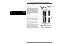
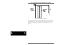
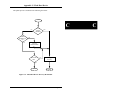
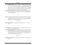
Configuring the EPC-5A
The EPC-5A can be user-configured to provide standard VMEbus Slot-1
functionality. The Slot-1 configuration option is enabled (default) by installing the
Slot-1 shunt (jumper) on the processor board (see Figure 1, page 4). Removing the
jumper disables Slot-1 functionality. When the EPC-5A is configured as the Slot-1
controller, it performs all the standard VMEbus system control functions. See
Chapter 5, Theory of Operation, for more details on Slot-1 controller functions.
Page 7
2
EPC-5A Hardware & Software Reference Manual
Slot-1 Controller
Jumper
2
2
P1
Front
Panel
P2
JP1
Jumpers
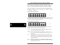
Figure 2-1. Slot-1 Jumper Location.
Additionally, the EPC-5A has another jumper (see Figure 2-1 above) that rarely needs
to be changed - the MODID jumper on JP1. The EPC-5A uses pin 30, Row A of the
P2 connector for module identification. If the J2 backplane is other than a standard
VME or VXI backplane (e.g., a VSB backplane) or Pin 30, Row A is defined for
another purpose, remove this jumper.
Selecting the EPC-5A Slot Location
There are two main considerations in determining where the EPC-5A should be
positioned in the chassis.
•
When used as a Slot-1 controller, and per the VMEbus specification (Rule
3.3), a Slot-1 controller must be in Slot 1. All other boards must be to the
right of the Slot-1 controller.
•
The EPC-5A connects to its peripherals via a subplane which extends to the
right of the EPC-5A. Make sure that the location you choose provides
sufficient room for all the attached peripherals (EXMs and mass storage
module).
Page 8
Chapter 2: Before Installation
The EPC-5A plus EXM expansion modules plus any mass storage module can be
considered together as a single subsystem. Use the following worksheet to determine
the total number of VME expansion interface slots your particular subsystem
configuration requires.
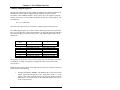
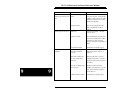
Product
VME Slots
EPC-5A
(Includes first two EXM modules)
Additional EXP-MC(s)
(Holds additional two EXM modules)
EXP-AM
Mass Storage Module (EXP-MX
including EXP-MX200A and greater)
or
EXP-MX200
2
Total
2
1
each
2
2
3
Total VMEbus slots used ...........................
Table 2-1. VME Slots Available.
Once you have determined where the EPC-5A subsystem will be physically located in
the chassis, the VME backplane must be jumpered appropriately.
Page 9
2
EPC-5A Hardware & Software Reference Manual
Installing the VMEbus Backplane Jumpers
2
2
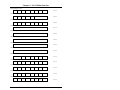
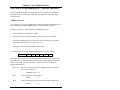
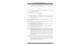
The VMEbus specification provides four bus grant signals (BG0 - BG3) and one
interrupt acknowledge signal (IACK) via daisy-chain lines. Per the VMEbus
specifications, all boards (that plug into the backplane) are required to correctly
handle these signals. All slots that do not have a board plugged into the backplane
(i.e. empty slots and slots occupied by EXMs or mass storage modules), need to be
jumpered to allow the signals to pass through to other boards in the system.
xxxIN
xxxIN
xxxIN
xxxIN
xxxOUT
xxxOUT
xxxOUT
xxxOUT
VMEbus Slots
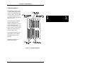
Figure 2-2. Daisy-Chain Signal Concept.
The Slot-1 controller board initiates each daisy-chain signal. Each VMEbus slot to
the right of the Slot-1 controller must pass through each of the daisy-chain signals.
For each VMEbus slot, xxxIn pin must be connected to its corresponding xxxOut
pin (e.g. BG0In to BG0Out, BG1In to BG1Out,...,IackIn to IackOut)
either through the board in that slot or by jumpers. Some boards correctly pass all of
these signals, some boards handle some of these signals and not others, and some
boards (typically “dumb” slave boards) may not handle any of these signals. Check
the manual for each board to be installed to determine if these signals are passed
through correctly. If they are not, or if the VMEbus slot is empty, all (or some) of
these signals must be jumpered. See the following figures for examples.
Page 10
Chapter 2: Before Installation
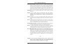
indicates jumper needed
2
Figure 2-3. Backplane Jumpers Required for EPC-5A Subsystem.
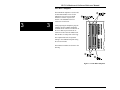
The figure above shows the EPC-5A subsystem. Note that the left-most slot
does not require any jumpers. All other slots occupied by the subsystem
require all five jumpers be installed.
Page 11
2
EPC-5A Hardware & Software Reference Manual
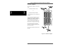
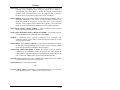
BG0
2
2
BG1
BG2
BG3
IACK
Single Board Computer
that only handles
IACK & BG3
"Dumb" Slave
Does not handle
any of the signals
Figure 2-4. VMEbus Backplane Jumper Examples.
Once you have determined where the jumpers need to be, you must determine how to
jumper your particular backplane. Different backplane manufacturers handle this in
different ways; some provide stake pins on the rear of the backplane while others
provide stake pins on the front of the backplane. These stake pins can be located in
several different places.
Page 12
Chapter 2: Before Installation
J1 Connector
J1 Connectors
BG0
BG1
BG2
BG3
BG0
BG1
BG2
BG3
IACK
IACK
Figure 2-5. VMEbus Jumpers
on Rear Wirewrap Pins.
2
Figure 2-6. VMEbus Jumpers
on Front Stake Pins.
If the stake pins are on the rear of the backplane, the most common location is in the
middle of the J1 connector as shown in Figure 2-5 below. This can be just these pins
extended or all pins extended for wirewrapping.
The stake pins (front or rear) can also be located adjacent to the slot being jumpered
as shown in Figure 2-6 above. Typically, the stake pins are located between the slot
being jumpered and the next lower-numbered slot (e.g. jumpers for Slot 6 would be
located adjacent to Slot 6 between Slots 5 and 6).
Consult your VME chassis reference manual or contact the chassis manufacturer if
you are unsure where to jumper your particular system.
Page 13
2
EPC-5A Hardware & Software Reference Manual
Jumpers
The complete table of EPC-5A jumpers is shown below. Jumpers are shown in Figure
2-1.
2
2
Jumper
POST
(JP1 [1-2])
FFLASH
(JP1[3-4])
BBEN
(JP1 [5-6])
FWEN
(JP1 [7-8])
Function
Manufacturing loop
enable
Force BIOS recovery
MODID
(JP1 [9-10])
SPEAKER
(H2)
SLOT1
(H5)
Mod ID routing
FBD boot block write
enable
FBD write enable (except
boot block)
Speaker
Slot 1 Functionality
Description
Install this jumper to enter the
manufacturing POST loop.
Install this jumper to force a BIOS
recovery during the boot process.
Install this jumper to enable writes
to the boot block of the FBD.
Install this jumper to enable writes
to the FBD main blocks #1, #3, and
#4 and parameter blocks #1 and #2.
Remove this jumper for nonstandard VME backplanes.
Speaker header.
Install this jumper to enable Slot 1
functionality.
Table 2-2. EPC-5A Jumpers.
Page 14
3. Installation
!
▲
▲
CAUTION
During all of this installation process, make sure that power to
your system is OFF.
The EPC-5A is not designed to be inserted or removed while the chassis is
powered up.
!
▲
▲
CAUTION
Make sure that the installation process described here is
performed in a static-free environment.
Do not remove any modules from their anti-static bags unless you are in a static-free
environment. The EPC-5A module, like most other electronic devices, is susceptible
to electrostatic discharge (ESD) damage. ESD damage is not always immediately obvious. It can cause a partial breakdown in semiconductor devices that might not result
in immediate failure.
!
▲
▲
CAUTION
The EXP-MX mass storage module contains a delicate hard
disk. Use care during installation.
Subplane Installation
Subplanes are printed-circuit boards with connectors on both sides. A subplane
provides several functions. Primarily it acts as the PC/AT bus. Additionally, it
provides power from the VMEbus backplane to the EPC-5A and expansion modules.
How subplanes function is discussed in detail in Chapter 5, Theory of Operation.
Locate the appropriate subsection for the subplane you are using either by name or
by picture. Follow the directions in the appropriate subsection. A small bag of bolts,
nylon washers, and nuts is provided for optionally securing the subplane to the VME
backplane. If these are used, be careful not to over tighten the bolts. Over-tightening
causes the subplane to bend and may cause EXM failure due to poor contact.
Page 15
3
3
EPC-5A Hardware & Software Reference Manual
EXP-BP2 Subplane
3
3
This subplane is used in the smallest
configuration, where only the EPC-5A
processor module occupies VME slot
space. It provides connectivity for two
EXM modules within the EPC-5A (e.g.,
a graphics controller and a network or
disk controller). The EXP-BP2 is an
L-shaped board with three connectors
on each side.
After jumpering the backplane, plug the
subplane into the VMEbus backplane
such that the P2 connector on the back
of the 4-row DIN is pressed into the J2
connector of the left-most VMEbus slot
that the EPC-5A subsystem will occupy.
The subplane has holes for optional
bolting to the VMEbus backplane using
the screws included.
The lower EXM connector is denoted as
EXM slot 0 and the upper as slot 1 as
shown in the diagram. This information
will be needed later when configuring the
installed EXMs.
Page 16
1
0
Figure 3-1. EXP-BP2 Subplane.
Chapter 3: Installation
EXP-BP4 Subplane
The EXP-BP4 subplane is used
to couple an EPC-5A processor
module with an EXP-MX Mass
Storage module. The EXP-BP4
is a T-shaped board with four
connectors on the front side and
three on the rear.
3
After jumpering the backplane,
plug the subplane into the
VMEbus backplane such that the
P2 connector on the back
of the 4-row DIN is pressed into
the J2 connector of the left-most
VMEbus slot that the EPC-5A
subsystem will occupy.
The subplane has holes for optional bolting to the VMEbus
backplane using the screws
included.
The EXM slot numbers are
shown in the drawing.
Figure 3-2. EXP-BP4 Subplane.
Page 17
3
EPC-5A Hardware & Software Reference Manual
EXP-BP3A Subplane
The EXP-BP3A subplane is used to add
an EXP-MC Module Carrier for the
addition of one or two more EXM
modules to an EPC-5A processor
module. The EXP-BP3A has five
connectors on each side.
3
3
After jumpering the backplane, plug the
subplane into the VMEbus backplane
such that the P2 connector on the back of
the 4-row DIN is pressed into the J2
connector of the left-most VMEbus slot
that the EPC-5A subsystem will occupy.
The subplane has holes for optional
bolting to the VMEbus backplane using
the screws included.
The EXM slot numbers are shown in the
drawing.
Figure 3-3. EXP-BP3A Subplane.
Page 18
Chapter 3: Installation
EXP-BP5 Subplane
The EXP-BP5 subplane is used
in a configuration to couple an
EPC-5A processor module with
an EXP-MC Module Carrier
and an EXP-MX Mass Storage
module. The EXP-BP5 has six
connectors on the front side and
five on the rear.
3
After jumpering the backplane, plug the subplane into
the VMEbus backplane such
that the P2 connector on the
back of the 4-row DIN is
pressed into the J2 connector of
the left-most VMEbus slot that
the EPC-5A subsystem will
occupy.
The subplane has holes for optional bolting to the VMEbus
backplane using the screws
included.
The EXM slot numbers are
shown in the drawing.
Figure 3-4. EXP-BP5 Subplane.
Page 19
3
EPC-5A Hardware & Software Reference Manual
EXP-BP4A Subplane
The EXP-BP4A subplane is used to add
either
•
two EXP-MC Module Carriers
or
3
3
•
one EXP-AM Adapter Module.
The EXP-BP4A has seven connectors on
each side.
After jumpering the backplane, plug the
subplane into the VMEbus backplane
such that the P2 connector on the back of
the 4-row DIN is pressed into the J2
connector of the left-most VMEbus slot
that the EPC-5A subsystem will occupy.
The subplane has holes for optional
bolting to the VMEbus backplane using
the screws included.
The EXM slot numbers are shown in the
drawing.
Figure 3-5. EXP-BP4A Subplane.
Page 20
Chapter 3: Installation
EXP-BP6 Subplane
The EXP-BP6 subplane is used
in a configuration to couple an
EPC-5A processor module with
an EXP-MX Mass Storage
module and either
•
3
two EXP-MC Module
Carriers
or
•
one EXP-AM
Adapter Module.
The EXP-BP6 has eight
connectors on the front side
and seven on the rear.
Plug the subplane into the
VMEbus backplane such that
the P2 connector on the back of
the 4-row DIN is pressed into
the J2 connector of the leftmost VMEbus slot that the
EPC-5A subsystem will
occupy.
Figure 3-6. EXP-BP6 Subplane.
The subplane has holes for optional bolting to the VMEbus
backplane using the screws included.
The EXM slot numbers are shown in the drawing.
Page 21
3
EPC-5A Hardware & Software Reference Manual
EPC-5A Insertion
After installing the subplane, the EPC-5A processor module can be inserted into the
VMEbus chassis.
!
▲
3
3
!
▲
CAUTION
Make sure that power to your VME system is off. The EPC-5A
module is not designed to be inserted or removed from a live
backplane.
CAUTION
When inserting the EPC-5A module, avoid touching the circuit
board and connector pins, and make sure the environment is
static-free.
q
Make sure the ejector handles are in the normal (non-eject) position. (Push
the top handle down and the bottom handle up so that the handles are not
tilted.)
q
Slide the EPC-5A module into the left-most slot occupied by the subplane.
Use firm pressure on the handles to mate the module with the connectors.
q
Tighten the retaining screws in the top and bottom of the front panel to
ensure proper connector mating and prevent loosening of the module due to
vibration.
Page 22
Chapter 3: Installation
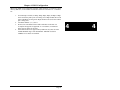
EXP-MC Module Carrier Insertion
If one or more EXP-MC Module Carriers are part of the configuration, they are
inserted into the slot(s) immediately to the right of the EPC-5A. The Module Carrier
can only be used in a VMEbus slot where the subplane has both EXM connectors.
Simply slide the Module Carrier into place and tighten the two top and bottom
retaining screws.
The following figure shows a side view of an EXP-MC containing two EXMs plugged
into a subplane that is plugged into a VMEbus backplane.
EXP-MC Module Carrier
Subplane
VMEbus
Backplane
EXM
Expansion Module
EXM
Expansion Module
Figure 3-7. EXP-MC Module Carrier (side view).
Page 23
3
3
EPC-5A Hardware & Software Reference Manual
EXP-MX Mass Storage Module Insertion
!
▲
!
▲
3
3
CAUTION
Handle the mass storage module with care. Avoid sudden drops
or jolts.
CAUTION
When inserting the module, avoid touching the circuit board and
connector pins, and make sure the environment is static-free.
The EXM-MX Mass Storage module is always inserted as the rightmost module of the
EPC-5A subsystem. Insert it so that its rear connector mates with the lower rightmost
connector of the subplane. Insert it using adequate continuous force rather than
tapping or hammering on it. Tighten the top and bottom front-panel screws to hold it
firmly in place.
EXM Module Insertion
One or two EXMs may be installed through the front panels of the EPC-5A and each
EXP-MC Module Carrier. To install an EXM:
q
Remove and save the blank face plate from the desired slot.
q
Slide the EXM into place in the card guides. Push firmly on the EXM front
panel until the EXM card-edge connector is firmly seated in the subplane
connector.
q
Tighten the thumb screws on the EXM’s face plate.
Each EXM must be configured in the EPC-5A’s BIOS to set how the EXM should be
initialized on power-up. This information is slot specific. Although EXMs can be
installed in any available carrier slot, once an EXM is installed, it cannot be moved
without re-configuring the BIOS setup. Configuring the BIOS setup is discussed in
the next chapter.
Page 24
Chapter 3: Installation
Connecting Peripherals to the EPC-5A
!
▲
CAUTION
Do not plug in any cable connector into the front panel
connectors while the system is powered on. In general,
electronic equipment is not designed to withstand potential
damage that could arise from fluctuations in power. Never plug
in a serial or parallel device, keyboard, transceiver, monitor, or
other component while the system is on.
The final step of installation is connecting peripherals, typically a video display and
keyboard, but also perhaps a mouse, modem, printer, etc. Unless otherwise noted, all
connectors are compatible with those found on IBM-compatible desktop PCs, and
therefore pin-by-pin details are not given in this chapter. Pin-outs are specified in
Chapter 7, Connectors.
Monitor
Connection of a monitor requires the use of an EXM video controller. Consult the
video controller manual for details.
The monitor should be attached and powered on prior to applying power to the
EPC-5A. If this is not done, the EPC-5A cannot detect the monitor type and the
video adapter may not be initialized correctly.
Keyboard
The front panel contains a round 6-pin mini-DIN jack for connecting a keyboard. The
jack is compatible with that of some newer PCs, and is not compatible with the
previous style of larger 5-pin PC/AT keyboard connectors. However, an adapter
cable is provided with the EPC-5A so either type of PC keyboard can be used with the
EPC-5A.
Page 25
3
3
EPC-5A Hardware & Software Reference Manual
Serial Ports
The front panel contains two DB-9 DTE serial-port connectors. They are standard
RS-232 serial communication ports that are 16C450-compatible. Many current PC/AT
computers now incorporate 16C550 UARTs.
The EPC-5A serial ports may be used for connecting a mouse, modem, serial printer,
RS-232 link, etc.
3
3
Parallel Printer Port
The output-only parallel port on the front panel is a DB-25 connector that is
completely compatible with the corresponding LPT1 connector on IBM PCs and
compatibles. Typically it is used to connect printers and software security keys.
Page 26
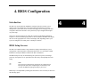
4. BIOS Configuration
Introduction
The EPC-5A uses the Phoenix NuBIOS to configure and select various system
options. This section details the various menus and sub-menus that are used to
configure the system. This section is written as though you are setting up each field
in sequence and for the first time. Your system may be pre-configured and require
very little setup.
Some error messages might occur during the execution of the BIOS initialization
sequence. If errors occur during the power-on self-test (POST), the BIOS will display
the error on the appropriate line of the screen display and, depending on how your
system is configured, will either pause or attempt to continue.
BIOS Setup Screens
The EPC-5A’s BIOS contains a setup function to display and modify the system
configuration. This information is maintained in the EPC-5A’s nonvolatile CMOS
RAM and is used by the BIOS to initialize the EPC-5A hardware.
The BIOS Setup can only be entered during the system reset process, following a
power-up, front panel reset, or equivalent. Press the F2 key when prompted to enter
Setup.
✏
Note
The “Press F2 to Enter Setup” prompt may be suppressed (see
Boot Options Sub-menu, Setup Prompt), but the F2 key still
invokes the BIOS Setup program during system reset.
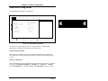
BIOS setup is accomplished by making selections from a series of menus, as shown in
the following figure.
Page 27
4
4
EPC-5A Hardware & Software Reference Manual
Main BIOS Setup Menu
MAIN
4
IDE Adapter
Sub-Menu
4
Memory Shadow
Sub-Menu
ADVANCED EXM
VME
EXIT
EXM Menu
VME Menu
Advanced Menu
Exit Menu
Boot Sequence
Sub-Menu
Keyboard Features
Sub-Menu
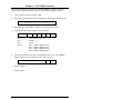
Figure 4-1. BIOS Setup Menu Map.
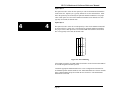
Use the up and down cursor (arrow) keys to move from field to field. Use the right
and left arrows to move between the menus shown in the menu bar at the top of the
screen. If you use the arrow keys to leave a menu and then return, your active field is
always at the beginning of the menu. If you select a sub-menu and then return to the
main menu, you return to that sub-menu heading.
Fields with a triangle to the left are actually sub-menu headings; press Enter when
the cursor rests on one of these headings to reach that sub-menu. For most fields,
position the cursor at the field and from the numeric keypad, press the + and - keys
to rotate through the available choices. Certain numeric fields can also be entered via
the keyboard. Once the entry has been changed to appear as desired, use the up and
down arrow to move to the next field.
Page 28
Chapter 4: BIOS Configuration
Main BIOS Setup Menu
The Main BIOS Setup Menu is shown below.
PhoenixBIOS Setup - Copyright 1985-96 Phoenix Technologies Ltd.
Main
Advanced
EXM
System Time:
System Date:
Diskette A:
Diskette B:
IDE Adapter 0 Master:
IDE Adapter 0 Slave:
Video System:
Memory Shadow
Boot Sequence:
Numlock:
System Memory:
Extended Memory:
F1
ESC
Help
Exit
VME
[16:17:18]
[03/01/96]
[Not Installed]
[Not Installed]
(C: 704 Mb)
(None)
[EGA / VGA]
Exit
Item Specific Help
<Tab>, <Shift-Tab>, or
<Enter> selects field.
[A: then C:]
[Off]
640 KB
31 MB
Select Item
Select Menu
-/+ Change Values
Enter Select Sub-Menu
F9 Setup Defaults
F10 Previous Values
Figure 4-2. Main BIOS Setup Menu.
The fields in each menu and sub-menu are explained below. Additional help
information is available in the help area on the Setup screen.
System Time:/System Date
These values are changed by moving to each field and typing in the desired entry.
Use the Tab key to move from hours to minutes to seconds, or from months to days
to years.
Diskette A:/Diskette B
This field identifies the type of floppy disk drive installed as the A:/B: drive. Possible
settings are Not Installed, 360 KB, 5¼", 720 KB, 3½", 1.2 MB, 5¼", 1.44 MB,
3½", and 2.88 MB, 3½". The BIOS defaults to Not Installed for drives A: and B:.
Page 29
4
4
EPC-5A Hardware & Software Reference Manual
IDE Adapter 0 Master/Slave: Sub-menus
These fields are headings for menus that allow entering complete disk drive
information. Once the information is entered for the drive, the entry in the Main
Menu shows the drive selected. See IDE Adapter Sub-Menus for more information.
Video System
4
4
Use this field to select among the different video options available. Select from
EGA/VGA, CGA 80x25, or monochrome. The default is “EGA/VGA”. The
EPC-5A’s video is VGA, supplied by an EXM Video Module.
Memory Shadow Sub-menu
The term “Memory Shadow” refers to the technique of copying information from an
extension ROM into DRAM and accessing it in this alternate memory location. See
Memory Shadow Sub-Menu for more information.
Boot Sequence Sub-menu
The Boot Sequence Sub-menu allows you to change the boot delay, the boot
sequence, and to disable several displays during the boot process, such as the
SETUP prompt, POST errors, floppy drive check, and summary screen. When the
boot sequence has been specified in the Boot Sequence sub-menu, the sequence
is displayed in the Boot Sequence field of the Main menu.
Keyboard Features (Numlock) Sub-menu
Use this menu to enable or disable various keyboard features, including the Numlock
key, the key click, and the keyboard auto-repeat rate and delay. The Numlock entry in
the Main Menu displays the Numlock setting.
System Memory
This field is not editable and displays the amount of conventional memory (below
1MB). No user interaction is required.
Extended Memory
This field is not editable and displays the amount of extended memory (above 1MB).
No user interaction is required.
Page 30
Chapter 4: BIOS Configuration
IDE Adapter Sub-menus
There are a total of two IDE adapter sub-menus for the primary hard disk controller,
in a master and slave drive configuration. The EPC-5A hard disk is controlled by the
settings for IDE Adapter 0 Master. To see or reconfigure the detailed characteristics
of the primary hard disk, select the IDE Adapter 0 Master item from the Main BIOS
Setup. The IDE Adapter 0 Master sub-menu is shown below.
PhoenixBIOS Setup - Copyright 1985-96 Phoenix Technologies Ltd.
IDE Adapter 0 Master
(C:
704Mb)
Item Specific Help
Autotype Fixed Disk:
[Press Enter]
Type:
Cylinders:
Heads:
Sectors/Track:
Write Precomp:
[User] 704 Mb
[ 1365]
[
16]
[
63]
[None]
LBA Mode Control:
[Disabled]
F1
ESC
Help
Exit
Select Item
Select Menu
<Tab>, <Shift-Tab>, or
<Enter> selects field.
-/+ Change Values
Enter Select Sub-Menu
F9 Setup Defaults
F10 Previous Values
Figure 4-3. IDE Adapter Sub-menu.
Autotype Fixed Disk
Use this option when setting up new disks. This option allows the BIOS to determine
the proper settings of the disk based on information on the disk, which is detected by
the EPC-5A BIOS for drives that comply with ANSI specifications. Press the Enter
key to invoke this function.
Existing (formatted) disks must be set up using the same parameters that were used
originally when the disk was formatted. You must enter the specific cylinder, head,
and sector information. This information is usually listed on the label attached to the
drive at the factory. Select the “User” type described below to describe an existing
formatted disk.
Page 31
4
4
EPC-5A Hardware & Software Reference Manual
Type
If you are using a pre-configured system, you probably have an IDE hard disk drive.
Select “None” if you are not using an IDE hard disk drive. In the case for which you
have an IDE disk but cannot employ the “Autotype” feature, then select “User” for the
Type and enter the correct drive values for cylinders, heads, sectors/track, and write
precompensation from the label attached at the factory. For disks not supplied by
RadiSys, consult the disk drive’s documentation.
4
4
If you specify “Auto” for the hard disk type, the BIOS will query the hard disk for its
parameters whenever the POST runs. If a hard disk type is set to “Auto”, but no hard
disk is actually present, the BIOS will continue to query the (non-existent) hard disk
until it times out, adding a number of seconds to the duration of the POST.
Note that there are some restrictions when setting up devices on the EPC-5A. If you
plan to boot from a non-IDE device, such as a SCSI hard disk, set the C: drive type as
“None” and use the BIOS extension.
LBA Mode Control
When enabled, this option allows the System BIOS to reference hard disk data as
logical blocks instead of using the traditional Cyliners/Heads/Sectors (CHS) method.
This option can only be used if both the hard disk being configured and the operating
system support Logical Block Addressing (LBA). If disabled, then CHS mode is used.
Note that autotyping may change this value if the hard disk reports that it supports
LBA. The default is “Disabled.”
Page 32
Chapter 4: BIOS Configuration
Memory Shadow Sub-Menu
The term “shadowing” refers to the technique of copying BIOS extensions from ROM
into DRAM and accessing them from DRAM. This allows the CPU to access the
BIOS extensions much more quickly and generally increases system performance if
many calls to the BIOS extensions are made. The Memory Shadow Sub-menu is
shown below.
PhoenixBIOS Setup - Copyright 1985-96 Phoenix Technologies Ltd.
Memory Shadow
Item Specific Help
System Shadow:
Video Shadow:
Enabled
Enabled
<Tab>, <Shift-Tab>, or
<Enter> selects field.
Regions with Legacy Expansion ROMs:
C800-CBFF:
[Disabled]
CC00-CFFF:
[Disabled]
D000-D3FF:
[Disabled]
D400-D7FF:
[Disabled]
D800-DBFF:
[Disabled]
DC00-DFFF:
[Disabled]
F1
ESC
Help
Exit
Select Item
Select Menu
-/+ Change Values
Enter Select Sub-Menu
F9 Setup Defaults
F10 Previous Values
Figure 4-4. Memory Shadow Menu.
The shadow regions should be used only if an EXMbus card is installed in the system
that contains a BIOS extension (ROM) although there is no effect on the system if a
region is shadowed that does not contain a BIOS extension. Note that each shadow
region in the setup menu is 16KB in size. Multiple shadow regions may have to be
enabled if the BIOS extension to be shadowed is larger than 16KB.
System Shadow/Video Shadow
These options are not editable since the System and VGA BIOS are always shadowed.
Shadow Memory Regions
These options enable or disable shadowing for the associated memory region. The
default is “Disabled”.
Page 33
4
4
EPC-5A Hardware & Software Reference Manual
Boot Options Sub-menu
Use the Boot Options sub-menu to change the boot sequence options. Select the Boot
Options sub-menu by clicking on the Boot Sequence item in the Main BIOS Setup
screen. The Boot Options Sub-menu is shown below.
PhoenixBIOS Setup - Copyright 1985-96 Phoenix Technologies Ltd.
Boot Options
4
4
Item Specific Help
Boot Delay:
Boot Sequence:
SETUP Prompt:
POST Errors:
Floppy Check:
Summary Screen:
F1
ESC
Help
Exit
[0]
[A: then C:]
[Enabled]
[Enabled]
[Enabled]
[Enabled]
Select Item
Select Menu
<Tab>, <Shift-Tab>, or
<Enter> selects field.
-/+ Change Values
Enter Select Sub-Menu
F9 Setup Defaults
F10 Previous Values
Figure 4-5. Boot Options Sub-menu.
Boot Delay
Use this option to set the system to delay booting for a time period from 0 through 255
seconds. This allows for long start up times on boot devices that spin up slowly. The
default is “0” seconds.
Boot Sequence
This option is used to define how the system treats floppy drive A: when booting.
Booting can occur from a floppy in the A: drive or directly from the fixed disk drive.
To reduce the amount of time required to boot, the boot sequence should be set to “C:
only”. Note that the C: drive may be either an IDE, VME or Flash drive. The options
are as follows:
1. A: then C:
Page 34
Used to boot from the floppy drive, or if no floppy disk is
present in the A: drive, boot from the C: drive.
Chapter 4: BIOS Configuration
2. C: then A:
Used to boot from the C: drive, or if none is present, boot
from the A: drive.
3. C: only:
Used to boot from the C: drive without searching for an A:
drive.
The default is “A: then C:”.
The setting chosen here displays in the Boot Sequence Sub-Menu prompt in the Main
BIOS Setup screen.
Setup Prompt
This option is used to enable or disable the message “Press F2 to enter Setup.” Even
if the message is disabled, the F2 key can still be pressed at the appropriate time to
enter the Setup Menu. The default is “Enabled”.
POST Errors
This option is used to stop during the boot process if the POST encounters errors.
Otherwise, the system continues to attempt to boot despite any startup error messages
that display. Note that this option only affects those errors defined as boot failures.
See Chapter 9, Troubleshooting and Error Messages, for a list of those failures
defined as boot failures that are configured to halt the system. The default is
“Enabled”.
Floppy Check
This option is used to enable or disable the floppy drive search during the boot. To
speed up booting, the floppy check should be disabled. It is still possible to boot from
the A: drive even with the floppy check disabled. The default is “Enabled”.
Summary Screen
This option is used to enable or disable a summary of the system configuration, which
displays before the operating system starts to load. To speed up booting, disable the
summary screen. The default is “Enabled”.
Page 35
4
4
EPC-5A Hardware & Software Reference Manual
Keyboard Features Sub-menu
The Keyboard Features Sub-menu allows you to enable or disable various keyboard
features. To access the keyboard Features menu, select Numlock in the Main BIOS
Setup screen. The Keyboard Features Sub-menu is shown below.
PhoenixBIOS Setup - Copyright 1985-96 Phoenix Technologies Ltd.
Keyboard Features
4
4
Item Specific Help
NumLock:
Key Click:
Keyboard auto-repeat rate:
Keyboard auto-repeat delay:
F1
ESC
Help
Exit
Select Item
Select Menu
[On]
[Disabled]
[30/sec]
[1/4 sec]
<Tab>, <Shift-Tab>, or
<Enter> selects field.
-/+ Change Values
Enter Select Sub-Menu
F9 Setup Defaults
F10 Previous Values
Figure 4-6. Keyboard Features Sub-menu.
Numlock
Use this option to enable or disable the Numlock feature of the keyboard. Numlock on
enables the use of the keypad numbers. The default is “Auto.”
Key Click
Use this option to enable or disable the key click feature on the keyboard. If enabled,
the keyboard produces an audible click each time a key is pressed. The default is
“Disabled”.
Keyboard auto-repeat rate
Use this option to set the auto-repeat rate if you hold a key down on the keyboard. The
rate can be set to one of: “2/sec”, “6/sec”, “10/sec”, “13.3/sec”, “18.5/sec”,
“21.8/sec”, 26.7/sec”, and “30/sec”. The default rate is “30/sec”.
Page 36
Chapter 4: BIOS Configuration
Keyboard auto-repeat delay
Use this option to set the delay between when a key is pressed and when the autorepeat feature begins. The options are “1/4 sec”, “1/2 sec”, “3/4 sec”, and “1 sec” .
The default delay is “1/4 sec”.
When you are finished with this menu, press ESC to exit back to the Main BIOS
Setup screen.
4
Advanced Menu
This menu controls advanced setup features, such as the 486 internal L1 cache , large
disk access modes, and user BIOS extension addresses. You access this menu by
selecting Advanced from the Main BIOS Setup menu.
PhoenixBIOS Setup - Copyright 1985-96 Phoenix Technologies Ltd.
Main
Advanced
EXM
VME
Exit
Warning!
Item Specific Help
Setting items on this menu to incorrect values
may cause your system to malfunction.
L1 Cache
[Enabled]
Large Disk Access Mode:
[DOS]
User BIOS Extensions
BIOS Extension 1
BIOS Extension Offset in FBD:
Destination Address:
BIOS Extension Size:
[Disabled]
[D0000H]
[2000H]
F1
ESC
Help
Exit
↑↓ Select Item
← → Select Menu
<Tab>, <Shift-Tab>, or
<Enter> selects field.
-/+ Change Values
Enter Select Sub-Menu
F9 Setup Defaults
F10 Previous Values
Figure 4-7. Advanced Menu.
L1 Cache
This option controls the internal cache. The default is enabled. Disabling the internal
cache can negatively impact system performance.
Page 37
4
EPC-5A Hardware & Software Reference Manual
Large Disk Access Mode
If a hard disk larger than 528MB is being used, this selection should be set to “DOS”
if running MS-DOS, or set to “Other” if using a different operating system. When set
to “DOS”, this selection causes the System BIOS to perform cylinder/head translation
if the drive is configured in Setup to have more than 1024 cylinders. The default is
“DOS”.
User BIOS Extensions
4
4
These items control the loading (shadowing) of BIOS extensions contained in the
FBD main block #3. Note that there are actually three groups of Setup items to
control the shadowing of up to three BIOS extensions. The screen graphic only shows
the first group.
Two extensions ship with the EPC-5A. The PicoFlash BIOS offset is 48000h, and the
size is 2000h. The vRom BIOS offset is 4A000h, and the size is 4000h.
BIOS Extension Offset in FBD
This option selects the source address of the BIOS extension located in the FBD. The
address is an offset from the base of the FBD. The offset range is between 46000h
through 5FFFFh in 8KB increments. The default is “Disabled”.
Destination Address
This option selects the target address of the BIOS extension which can range from
C0000h through DFFFFh in 8KB increments. The default is “C8000h”.
BIOS Extension Size
This option selects the number of bytes to copy from the FBD into shadow memory.
BIOS extension sizes can be selected in 8KB increments from 2000h through 10000h.
The default is “2000h”.
Page 38
Chapter 4: BIOS Configuration
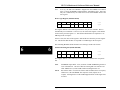
EXM Menu
Use the options in this menu to select and configure the available EXM slots.
The required configuration information is found in the hardware reference manual
shipped with each EXM expansion module. The EXM Menu is shown below.
PhoenixBIOS Setup - Copyright 1985-96 Phoenix Technologies Ltd.
Main
Advanced
EXM
VME
Exit
Item Specific Help
EXM Slot 0
ID:
Option
Option
EXM Slot 1
ID:
Option
Option
EXM Slot 2
ID:
Option
Option
EXM Slot 3
ID:
Option
Option
F1
ESC
Help
Exit
Byte 1
Byte 2
[FF]
[00]
[00]
Byte 1
Byte 2
[FF]
[00]
[00]
Byte 1
Byte 2
[FF]
[00]
[00]
Byte 1
Byte 2
[FF]
[00]
[00]
↑↓ Select Item
← → Select Menu
<Tab>, <Shift-Tab>, or
<Enter> selects field.
-/+ Change Values
Enter Select Sub-Menu
F9 Setup Defaults
F10 Previous Values
Figure 4-8. EXM Menu.
ID
This option is used to select the EXM ID byte value for the EXM card intended to
reside in this slot. If the BIOS finds that the ID set with this option does not agree
with the ID of the card actually installed in the slot, an EXM configuration error
occurs and the card is not configured. For a slot with no EXM card installed, enter
FFh, the default value.
Page 39
4
4
EPC-5A Hardware & Software Reference Manual
Option Byte 1
This option is used to select the first option byte value for the EXM card intended to
reside in this slot. Option byte 1 typically defines bit 0 as the card enable bit. Other
bits in the option byte are defined by the particular EXM card installed. The proper
value of this option for a slot with no EXM card installed is not defined. The value
typically used is 00h, the default value.
Option Byte 2
4
4
This option is used to select the second option byte value for the EXM card intended
to reside in this slot. Option byte 2 is defined by the particular EXM card installed.
The proper value of this option for a slot with no EXM card installed is not defined.
The value typically used is 00h, the default value.
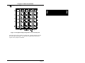
C 1
P
U
3
5
0
2
4
Figure 4-9. Slot Numbering.
All slots not occupied by an EXM module should show an ID of FF and OB1/OB2 of
00 00 indicating that no EXM is present.
Consult the appropriate EXM manual for the correct configuration information for
each EXM expansion module installed. Note: Most EXM hardware reference manuals
depict a different BIOS Setup Screen than the one shown here. The ID/OB1/OB2
information is still valid.
Page 40
Chapter 4: BIOS Configuration
When using EXMs with configurable interrupts, DMA channels, I/O addresses, and/or
memory addresses, avoid conflicts with built-in functions of the EPC-5A. Guidelines
are:
1.
2.
3.
4.
If an interrupt is needed, use IRQ3, IRQ4, IRQ5, IRQ9, or IRQ15. IRQ7
can be used if the printer port is not being used. IRQ3 should not be used
if the COM B port is being used. IRQ4 should not be used if the COM A
port is being used.
Use DMA channels 1, 3, 6, and 7.
Do not select I/O addresses that conflict with those in the EPC-5A.
A complete list appears in Appendix A. For instance, I/O addresses
in the 300-33F range can be used.
If the EXM needs to use upper memory addresses, they must be in the
C8000h-DFFFFh range. Note that E0000h - 0EFFFFh is used for
VMEbus access and is not available.
Page 41
4
4
EPC-5A Hardware & Software Reference Manual
VME Menu
The options in the VME menu are used to configure the EPC-5A’s VME interface.
The VME Menu is shown below.
PhoenixBIOS Setup - Copyright 1985-96 Phoenix Technologies Ltd.
Main
4
4
Advanced
EXM
VME
Exit
Item Specific Help
Arbitration Priority:
Arbitration Mode:
Bus Release:
ULA:
VME Boot Scan Range:
Slave Memory Offset:
F1
ESC
Help
Exit
[0]
[Round Robin]
[RONR]
[FE00(F8)]
[A24 FF000000h-FFF00000h]
[Disabled]
Select Item
Select Menu
-/+ Change Values
Enter Select Sub-Menu
F9 Setup Defaults
F10 Previous Values
Figure 4-10. VME Setup Menu.
Arbitration Priority
This option is used to select among the four (0 through 3) VMEbus priority levels
used when the EPC-5A requests the bus for a VME access. Priority level 0 is the
lowest priority while priority level 3 is the highest priority. The default is priority
level “0”.
Arbitration Mode
This option is used to select the arbitration algorithm that the EPC-5A’s VMEbus
arbiter uses when the EPC-5A is the slot 1 controller. Selecting “Round Robin”
configures the arbiter to “scan” the bus request lines from highest priority down to
lowest priority and grant the bus to the first requester it finds. Selecting “Priority”
configures the arbiter to grant the bus to the highest priority requester at any time.
The default is “Round Robin”.
Page 42
Chapter 4: BIOS Configuration
Bus Release
This option is used to select the method that the EPC-5A uses to release the VMEbus
for other bus masters to use. Selecting “ROR” (Release on Request) allows the
EPC-5A to perform better since it releases the VMEbus only if another bus master
requests the bus. Selecting “RONR” (Request on No Request – also known as VXI
fair-requester mode) causes the EPC-5A to release the VMEbus when its current bus
access has completed. This has the effect of increasing the performance of other bus
masters. The default is “ROR (VME)”.
4
Unique Logical Address
This option is used to select the ULA for the EPC-5A. This logical address is used to
uniquely identify and access the EPC-5A in a VXI system. The default is ULA “F8”.
VME Boot Scan Range
This option is used to select the scan range when booting from VME (vROM). The
ranges are as follows:
A24SD searches from FF000000h - FFF00000h on 100000h boundaries
A24SD searches from 00000000h - 00F00000h on 100000h boundaries
A32SD searches from 00000000h - FFF00000h on 100000h boundaries
Slave Memory Offset
This option is used to select the slave memory of the EPC-5A. Possible selections are:
18000000h (A32)
19000000h (A32)
1A000000h (A32)
1B000000h (A32)
1C000000h (A32)
1D000000h (A32)
1E000000h (A32)
1F000000h (A32)
000000h (A24)
400000h (A24)
800000h (A24)
C00000h (A24)
disabled (default)
Page 43
4
EPC-5A Hardware & Software Reference Manual
Exit Menu
The options in this menu allow saving settings and exiting, or abandoning changes and
exiting to the system, or controlling the backup and restoration of CMOS RAM to the
FBD. The Exit Menu is shown below.
PhoenixBIOS Setup - Copyright 1985-96 Phoenix Technologies Ltd.
4
4
Main
Advanced
EXM
VME
Exit
Item Specific Help
Save Changes & Exit
Discard Changes & Exit
Get Default Values
Backup CMOS to Flash
Restore CMOS from Flash
Restore Condition
Load Previous Values
Save Changes
Exit & Update BIOS
F1
ESC
Help
Exit
<Tab>, <Shift-Tab>, or
<Enter> selects field.
[Never]
Select Item
Select Menu
-/+ Change Values
Enter Select Sub-Menu
F9 Setup Defaults
F10 Previous Values
Figure 4-11. Exit Menu.
About CMOS Backup and Restore
You can save and restore your setup configuration in preparation for an event such as
battery failure or corrupt CMOS RAM. This feature also allows systems without
batteries to boot properly while still allowing you to configure the system via Setup,
which stores user settings in CMOS RAM. This feature allows automatic or manual
restoration, and selective CMOS RAM restore conditions.
The CMOS RAM configuration backup is stored in FBD parameter block #2. This
entire block is reserved for this purpose and cannot be shared.
The available selections from the Exit setup menu that would force a CMOS
restoration are: Always restore, Never restore, and restore on Corrupt CMOS. The
default setting is to restore on Corrupt CMOS.
Page 44
Chapter 4: BIOS Configuration
The System BIOS software searches the FBD for the unterminated string
“RadiSysCMOS--->” at power-up. This footprint marks the beginning of the CMOS
parameter block storage structure. The structure contains a 16-bit CRC of the CMOS
RAM data that is calculated at backup time and recalculated at restoration time. If the
CRC verification fails, the restoration is skipped.
If the System BIOS succeeds in restoring a backup image to CMOS RAM, the system
beeps 1 long and 5 short tones.
Restoration is inhibited for warm boots (CTRL-ALT-DEL from DOS) and when a
restore is attempted but no valid CMOS image exists in the FBD.
Save Changes & Exit
This option is used to save into CMOS the values that have been entered, then reboot.
Discard Changes & Exit
This option is used to discard the changes just made and revert to the state when Setup
was entered. The system reboots with the old values.
Get default values
This option is used to reset the Setup values to the original, default values that were
set at the factory, before any suppliers or other end users made changes.
Backup CMOS to Flash
This option is used to immediately save current Setup settings from CMOS into flash.
This is useful for backing up complicated setups.
Restore CMOS from Flash
This option is used to immediately restore CMOS settings from flash.
Restore Condition
This option is used to determine under what conditions the System BIOS restores
CMOS RAM from the FBD when booting. The restore conditions are: “Always”,
“Never”, and “Bad CMOS”. The default is “Bad CMOS”.
Page 45
4
4
EPC-5A Hardware & Software Reference Manual
Load previous values
This option is used to load the system with the previous values before an editing
session started.
Save Changes
4
4
This option is used to save the edits made during a session.
Exit & Update BIOS
This option is used to initiate a System BIOS update.
✏
Note
Do not select this exit option unless you have already obtained
BIOS update replacement software from your supplier and have
reviewed the documentation and procedures provided with that
distribution.
If you select this option by mistake, any changes made to the BIOS are lost unless you
have already saved them using the Save Current Values option. The system
automatically begins searching for the update program that should be on the floppy
disk inserted in drive A. If there is no floppy, you get two series of beep codes: a long
and two short beeps, followed by three short beeps that repeat. Cycle the power to
reset the system to its previous state.
Page 46
5. Theory of Operation
The EPC-5A is a PC/AT compatible processor. Most of the standard functions of the
PC architecture is embodied in the RadiSys R400 chip set. In addition, the EPC-5A
has two proprietary interfaces: one for the EXM expansion interface and the other for
the VMEbus.
Processor board
The EPC-5A processor board conforms with the VMEbus standard 6U form-factor.
Processor and Coprocessor
The processor in the EPC-5A is an Intel486-DX4 running internally at 100 MHz with
an external interface at 33 MHz.
The 486 has a built-in math coprocessor and 16K cache.
Core Logic
The system uses the RadiSys R400EX system controller. The R400EX was developed
by RadiSys to provide flexibility (of different system designs), ease of use, and low
system cost. It is intended as a long-life core logic solution for the 486.
Page 47
5
5
EPC-5A Hardware & Software Reference Manual
The core logic system support provided by the R400EX includes the following:
RadiSys
R400EX
PCCompatible
Features
5
RadiSys
R400EX
Core System
Support
Features
5
Real Time Clock
Keyboard/Mouse
Controller
Cache
Shadow
PC Speaker/Port B
Functionality
DRAM Refresh
Controller
Power
Management
Support
Programmable
Chip Select Units
(4)
IDE Interface
Provides Motorola 146818Acompatible real time clock and
alarm with 114 bytes of batterybacked CMOS memory. The RTC
also generates a periodic interrupt.
Access to the CMOS memory is
through registers 070h and 071h in
an index/data fashion.
Implements a 8042-Compatible
keyboard controller.
Supports L1 write-through cache.
Shadow BIOS in DRAM.
Port B register is located at 061h.
Supports two banks of SIMMs as
Fast Page Mode (FPM), Extended
Data Out (EDO) or Flash SIMMs.
Second bank start address is
configurable. Supports EDO/FPM
memory type detection. SIMM
types cannot be mixed.
This interface is not used on the
EPC-5A.
This interface is not used on the
EPC-5A.
This interface is not used on the
EPC-5A.
Table 5-1. R400EX Features.
Memory
The following memory options are available: 4 MB, 8 MB, 16 MB, 32 MB and
64 MB. (Check with RadiSys Technical Support for 128 MB and 256 MB
configurations.) Two SIMM sockets are available. See Chapter 8, Upgrades, for
memory upgrade instructions.
Page 48
Chapter 5: Theory of Operation
Memory Map
The 232 byte physical address space seen by the Intel486 occupies three areas:
1.
Addresses between 0 and 1 MB, which are largely defined by the IBM
PC/AT architecture.
2.
Addresses between 1 MB and 256 MB, which largely depend on how
much DRAM is installed in the EPC-5A.
3.
Addresses above 256 MB, which provide direct mapping to the VMEbus
with a variety of address modifiers and byte orderings. See Chapter 6,
The VMEbus Interface, for more information about this feature.
Memory at addresses between 0 and 1 MB (0FFFFFh) is mapped as follows:
Range
000000 - 09FFFF
0A0000 - 0BFFFF
Content
DRAM (first 640 KB)
Mapped to EXM interface; almost always used by a
video controller as video RAM
0C0000 - 0C7FFF
Write-protected DRAM containing video BIOS
0C8000 - 0DFFFF*
Uncommitted; mapped to EXM interface
0E0000 - 0EFFFF
User-mappable hardware window onto VMEbus
0F0000 - 0FFFFF
Write-protected DRAM containing BIOS
* 0C8000 - 0DFFFF may be used either as page frames (i.e. for Ethernet, etc.) or
may be used by DOS as upper memory blocks if an EMM driver is installed or
may be used for BIOS extensions.
For a 4 MB EPC-5A, the extended memory address space is defined as
00100000
00400000
003FFFFF 3 MB DRAM extended memory
00FEFFFF Uncommitted; mapped to EXM interface
For an 8 MB EPC-5A, the extended memory address space is defined as
00100000
00800000
007FFFFF 7 MB DRAM extended memory
00FEFFFF Uncommitted; mapped to EXM interface
For a 16 MB EPC-5A, the extended memory address space is defined as
00100000
00FFFFFF 16384 KB DRAM extended memory
Page 49
5
5
EPC-5A Hardware & Software Reference Manual
For a 32 MB EPC-5A, the extended memory address space is defined as
00100000
01FFFFFF 32764 KB DRAM extended memory
For a 64 MB EPC-5A, the extended memory address space is defined as
00100000
20000000
65536 KB DRAM extended memory
Note that since the EXM expansion interface has 24 address lines, some of the
“uncommitted; mapped to EXM interface” address areas map repeatedly, or wraparound, in the EXM interface's address space.
Peripheral Components
5
5
The EPC-5A uses the TI-16C452 controller to provide legacy I/O device support.
This chip provides two NS16C450-compatible serial ports and a parallel port. Since
LPTOEN ties to low, this port is output-only.
The serial ports signal interrupts on IRQ3 and IRQ4 and are accessible at the standard
PC-AT architecture I/O base addresses of 3F8h and 2F8h respectively. The parallel
port signals interrupts on IRQ7 and is accessible at the standard PC-AT architecture
I/O base address of 378h.
Real Time Clock
The system contains a real time clock module that is compatible with the Motorola
146818A. The RTC is implemented in the R400EX and contains 114 bytes of CMOS
RAM. The RTC and PC/AT CMOS RAM are addressable at the standard PC/AT
architecture I/O addresses of 70h and 71h and interrupts are signaled on IRQ8. The
System BIOS initializes the RTC on coldstarts if the RTC contains bad values.
Page 50
Chapter 5: Theory of Operation
Keyboard Controller
The R400EX contains an Intel 8042-compatible keyboard controller. The keyboard
controller is addressable at the standard PC-AT architecture I/O addresses of 60h and
64h. Keyboard interrupts are signaled on IRQ1.
ROM and ROM Shadowing
The EPC-5A contains a 28F004-B*-T Flash Boot Block. The Flash device is mapped
into the top of the processor’s 32-bit address space. The Flash device contains the PC
BIOS, some peripheral BIOS code, and user extensions.
For best possible performance, the BIOS initialization software copies the ROM
contents into DRAM (called shadowing) at addresses 0F0000-0FFFFF. The BIOS
also searches for the existence of a video adapter containing a video BIOS (e.g., an
EXM-13A). If a video BIOS is found, it is copied into the 0Cxxxx area of DRAM.
After copying into these areas, the BIOS write-protects them. Subsequent writes to
these areas complete successfully but do not alter the data.
Embedded Shadow
The EPC-5A supports several different boot methods and operating systems. In order
to boot from VME or flash, it is necessary to first load and execute a BIOS extension.
The FBD has an unused 96KB region in main block #3 that lies between the end of
the PicoFlash extension and start of the System BIOS that can be used for BIOS
extension storage. In order to use this area for BIOS extensions, it is necessary to first
program the image into the FBD (using REFLASH.EXE) and then, at run time, copy
the BIOS extension from the FBD into DRAM, and have the System BIOS scan that
region for BIOS extensions. Multiple BIOS extensions can be programmed into the
user block of the FBD. Setup items allow the user to select up to 3 BIOS extensions
in the FBD and load them into DRAM between C8000h through DFFFFh.
Bootable Device Precedence
There are several bootable devices for the EPC-5A. Depending on the configuration,
either the EXM-2A, VME, SCSI or IDE can be the boot device. This section
documents the order in which these devices are installed in the boot chain. BIOS
extensions supersede IDE as a bootable device.
Page 51
5
5
EPC-5A Hardware & Software Reference Manual
If there is more than one BIOS extension, the extension that is located at the highest
physical memory location is the first device in the boot chain.
Only two drives are visible as BIOS extensions.
The following denotes which devices are installed in the system when the devices are
enabled.
VME Booting: When booting from VME, the second BIOS recognized may be
SCSI. If SCSI is selected as the second BIOS recognized device, Flash can be
accessed under DOS by loading an OS-based driver. With this configuration,
IDE drives are not visible to the system.
SCSI Booting: If the boot device is SCSI, either VME or Flash can be selected
as the second BIOS recognized device. If VME is selected as the second BIOS
recognized device, Flash can be accessed under DOS by loading an OS-based
driver. IDE drives are not visible to the system.
5
5
Flash Booting: If the boot device is Flash, either VME or SCSI can be selected
as the second BIOS recognized device.
IDE Booting: If the boot device is IDE, either VME or Flash can be used only
after loading the device driver. SCSI can be selected as the second BIOSrecognized device.
Battery
The battery powers the CMOS RAM and TOD clock when system power is not
present. At 60°C, the battery should have a shelf life of over four years at 50% duty
cycle. In a system that is powered on much of the time and where the ambient poweroff temperature is less than 60°C, the battery is estimated to have a life of 10 years.
The battery supplied with the EPC-5A is mounted on the underside of the metal frame
and connected to a header on the processor board. Should the battery fail, you may
obtain and install a replacement from RadiSys Technical Support.
Replacing the battery is a simple task. However, removing the battery will invalidate
the CMOS setup parameters. It is recommended that all setup parameters be written
down while the battery is still good. Additionally, use the Backup CMOS to Flash
feature in the BIOS Exit Menu.
Page 52
Chapter 5: Theory of Operation
Video Controllers
The EPC-5A can operate with or without a video controller (such as the EXM-13B or
EXM-13A). The BIOS searches for an EXM having an EXM ID in the range
E8h-EFh (a range reserved for video controllers). The search is done by EXM slot
number, beginning at slot 0. If no EXM video adapter is found, the BIOS looks for a
PC add-in card video controller in an EXP-AM Adapter module. The error message
EXM CONFIGURATION ERROR may appear if the video controller EXM or the EXP-AM
has not been configured via the setup screen.
In either case, the BIOS automatically initializes and uses the first one found.
If no video controller is present, the BIOS operates without one. Programs that use
the standard operating system and BIOS character output functions can be run
successfully (the output is ignored). However, programs that rely on specific video
modes, that write directly into the video RAM, or that directly call video BIOS
functions will fail.
Front Panel LEDs
The EPC-5A has five LEDs in the top left corner of the front panel. These LEDs are
described below:
RUN
SYSFAIL
TEST
MASTER
SLAVE
This LED is lit whenever the EPC-5A’s CPU is performing bus cycles.
It first comes on at power-up and should remain lit as long as the
system is running.
This LED is only active when this EPC-5A is jumpered to be the
Slot-1 controller. It comes on whenever the system receives a
hardware reset and remains on until the initial power-on self-tests
have completed. It also comes on whenever the VMEbus SysFail line
is asserted.
This LED is lit whenever the system is running its power-on
self-test. This only occurs during a hardware reset.
The Master LED is lit whenever the EPC-5A is accessing the
VMEbus.
The Slave LED is lit whenever another master on the VMEbus is
accessing the EPC-5A’s memory.
Page 53
5
5
EPC-5A Hardware & Software Reference Manual
Resetting the EPC-5A
There are a number of ways to reset (reboot) the EPC-5A.
5
5
Power-off, Power-on
This causes all boards in the VMEbus to reset. The system runs the poweron self-tests and reboots the operating system.
Front-panel Reset button
The Reset button causes the EPC-5A to perform a hardware reset. The
system runs the power-on self-tests and reboots the operating system.
Ctrl+Alt+Del
This keyboard sequence is called a “warm boot”. The EPC-5A does not
reinitialize all of the processor's hardware. The power-on self-test does not
run. However, the operating system is reloaded.
VMEbus SysReset
The EPC-5A can be software-configured to respond or not respond to the
VMEbus SysReset line. Asserting this bit causes a hard reset of the system if
the VME YSRESET bit is asserted. See bit 7 (SRIE), register 8144h .
VMEbus Register Reset
The EPC-5A can also reset another master asserting the reset bit of a register
mapped to the VMEbus. Asserting this bit causes a hard reset of the system.
See bit 0 (RSTP), register 8144h.
EXM Expansion Interface
The EXM expansion interface is electrically similar to the PC/AT ISA (16-bit data)
bus. In addition, it contains a signal -EXMID used for dynamic recognition and
configuration of EXMs. EXMs respond to one or more I/O addresses in the range
100h - 107h only when their -EXMID line is asserted. EXMs are required to return a
unique EXM ID byte in response to a read from I/O address 100h.
This ID byte is the same identification byte discussed earlier in Chapter 4,
Configuring the BIOS Setup, in the section on the EXM Setup Menu.
The EXM expansion interface is provided on rows A, C, and D of the EPC-5A's
4-row DIN P2 connector. The subplane carries the EXM interface to other modules,
such as to EXM modules and the EXP-MX Mass Storage module. These EXM
interface signals are not passed through to the VMEbus.
Further information on the EXM expansion interface, its connectors, and standards for
building EXMs is available upon request.
Page 54
6. The VMEbus Interface
This chapter describes the EPC-5A VMEbus interface as seen by a program. Users
should avoid direct use of most of these facilities. Whenever possible, the VMEbus
interface should be accessed through the EPConnect software, an easy-to-use,
high-level interface that frees you from most machine-dependent considerations.
Connectivity
The EPC-5A module connects to the VMEbus J1 connector directly and uses all of the
defined VMEbus lines except SERCLK, SERDAT, and +5V STDBY. Connection
to the J2 connector is through the subplane’s 4-row DIN connector B row. The only
connections to the VME J2 backplane on the B row are power and ground, address
lines A31-A24, and data lines D16-D31. Pin 30, Row A, the VXI-defined module
identification (MODID) line is also connected. Pin A30 is an input driving one gate
input and an 825-ohm pull-down resistor. It may be disabled by removing the
MODID jumper on the EPC-5A. If necessary, see Chapter 2, Configuring the
EPC-5A.
VMEbus System (Slot-1) Controller Functions
Every VMEbus system must have a System (Slot-1) Controller. The Slot-1 controller
provides the following functionality:
•
Serves as the bus arbiter (priority or round-robin)
•
Drives the 16 MHz SYSCLK signal
•
Starts the IACK daisy chain
•
Provides Bus Timer function
Page 57
6
6
EPC-5A Hardware & Software Reference Manual
When configured as the Slot-1 controller, the EPC-5A detects and terminates data
transfer bus timeouts. Once it sees either the DS0 or DS1 lines asserted, a counter is
started. If the counter expires before both DS0 and DS1 are deasserted, the
EPC-5A asserts the VMEbus BERR signal until both data strobes are deasserted. The
duration of the VMEbus timeout counter is 100-120 µsecs. When the EPC-5A is
configured as the slot-1 controller, this timeout cannot be disabled and the duration
cannot be changed.
Although the EPC-5A provides the required timeout function for data transfer timeout, it does not provide the optional bus grant timeout. If another master has been
granted permission to use the data bus but does not access (or relinquish) the data bus,
the bus will be “hung” indefinitely.
Concepts
Memory Map
6
6
VMEbus accesses are available by mapping a 64K segment of the VMEbus through
the 0E0000h -0EFFFFh window or by direct mapping above 256 MB. The following
summarizes the source of the VMEbus address lines for accesses through the VME
memory window.
A32
31
2423
From
port
8150
2221
From
port
8151
1615
From
port
8130
0
From
486 address
bits 15-0
A24
23
From
port
8151
2221
1615
From
port
8130
0
From
486 address
bits 15-0
A16
15
0
From
486 address
bits 15-0
Figure 6-1. Source of VMEbus Address Lines (Via VME memory window).
Page 58
Chapter 6: The VMEbus Interface
It should be noted that the EPC-5A drives all 32 address lines even when performing
an A24 or A16 access. Therefore, all the above registers (8150, 8151, 8130) should
be set for every access using the VME memory window. Make sure that those
registers not directly supplying address lines are set to “FF” values in the appropriate
bit positions.
Direct VMEbus Accesses
An alternate way to perform VMEbus accesses, provided that the EPC-5A is running
in protected mode, is to perform reads and writes at 486 addresses above 10000000h
(256 MB). For instance, a 4-byte read at address 40000000h will result in a 4-byte
VMEbus read access at address 00000000 with an address modifier specifying A32,
supervisory data and no byte-swapping (little-endian mode).
With the EPC-5A, addresses above 256 MB, with one exception for PC compatibility,
map onto the VMEbus. When direct “protected-mode” addressing of A24 or A16
space, the high-order nibble is used to define the access mode and byte ordering. For
A32 space, the high-order 2 bits define the access mode leaving 30 bits available for
addressing. Thus, only the first 1 Gigabyte of VMEbus A32 space is directly
addressable. All A24 and A16 space is directly addressable. The chart following
shows how this direct mapping is used.
Address Range
Access Mode
1xxx0000 - 1xxxFFFF VME A16 supervisory data
2x000000 - 3xFFFFFF VME A24 supervisory data
40000000 - 7FFFFFFF VME A32 supervisory data
(mapped to VME 00000000-3FFFFFFF)
80000000 - BFFFFFFF VME A32 supervisory data
(mapped to VME 00000000-3FFFFFFF)
Cxxx0000 - DxxxFFFF VME A16 supervisory data
Ex000000 - ExFFFFFF VME A24 supervisory data
F0000000 - FFFEFFFF Mapped to EXM expansion interface
FFFF0000 - FFFFFFFF 486 upper ROM area
Byte Order
little endian
little endian
little endian
big endian
big endian
big endian
Table 6-1. Direct Mapping.
Page 59
EPC-5A Hardware & Software Reference Manual
When accessing the VMEbus in this manner, the source of the VMEbus address lines
is defined below.
A32
31 3029
0
00
From 486 address bits 29-0
A24
23
0
From 486 address bits 23-0
A16
15
0
From 486 address bits 15-0
Figure 6-2. Source of VMEbus Address Lines (Via Direct Mapping).
The main purpose of the direct VMEbus access mechanism, as opposed to the
VME memory window mechanism, is for multitasking 32-bit operating-system
environments, where multiple tasks need to make VMEbus accesses. Without this, the
tasks would have to coordinate their use of the VME memory window mapping
registers.
6
6
When using the EPC-5A this way to perform VMEbus accesses, one would typically
set up the VME memory window for interrupt acknowledge accesses. Also note that
the direct access mappings do not cover the entire VMEbus A32 address range and do
not provide all VMEbus-defined address modifier encodings, but one can use the
VME memory window mechanism if needed to provide these.
Byte Ordering
There are two fundamentally different ways of storing numerical values in byte locations in memory:
•
Little endian, characteristic of Intel microprocessors, where the
least-significant data byte (LSB) is stored in the lowest byte address.
Address + 3
Address + 2
Address + 1
Address
Byte 3
Byte 2
Byte 1
Byte 0
MSB
Page 60
LSB
Chapter 6: The VMEbus Interface
•
Big endian, characteristic of Motorola microprocessors and the VMEbus
environment in general, where the most-significant data byte (MSB) is
stored in the lowest byte address.
Address + 3
Address + 2
Address + 1
Address
Byte 3
Byte 2
Byte 1
Byte 0
LSB
MSB
The EPC-5A contains programmable byte-swapping hardware to allow programs to
read or write VMEbus memory in either byte order. When using the VME memory
window to access the VMEbus, the order is selected by bit 5 (BORD) in the VME
modifier register (8151).
When using direct memory mapping, the order is address-range dependent (e.g.,
E0000000-E0FFFFFF accesses the A24 space with big endian byte ordering, and
20000000-20FFFFFF accesses the A24 space with little endian byte ordering).
When performing a single byte (D08) access, the byte order makes no difference.
However, word (D16) or double-word (D32) accesses may require byte-swapping.
When little-endian is selected, bytes pass straight through unchanged. Little endian
should only be used when reading or writing data between two Intel processor
systems. The results of using little-endian byte ordering to transfer a double-word
integer between an Intel processor and a Motorola processor are shown below.
486
Address
Motorola
Address
Addr+3
Addr+2
Addr+1
Addr
76
54
32
10
Addr+3
Addr+2
Addr+1
Addr
76
54
32
10
= 76543210h
LSB
= 10325476h
MSB
Figure 6-3. Little-Endian Byte Order.
Since the 486 processor uses Addr as the least-significant byte and the Motorola
processor uses Addr as the most-significant byte, the processor receiving the data gets
a “scrambled” value.
When big-endian is selected, the bytes are swapped between the 486 and VME. See
the diagram below.
Page 61
EPC-5A Hardware & Software Reference Manual
D16
Access
D32
Access
Addr+1
Addr
32
10
LSB
Addr+1
Addr
10
32
486
Address
Motorola
MSB
Address
Addr+3
Addr+2
Addr+1
Addr
76
54
32
10
LSB
Addr+3
Addr+2
Addr+1
Addr
10
32
54
76
MSB
Figure 6-4. Big-Endian Byte-swapping.
When using big-endian byte ordering, care must be taken to assure that the VME
address is aligned on a boundary; for D16 accesses the VME address must be on a
word boundary (address evenly divisible by 2) and for D32 accesses the VME address
must be on a double-word boundary (evenly divisible by 4).
If this is not done, the results will be “scrambled” data. Although the VMEbus
address must be boundary-aligned to match the data width (word or double-word),
the 486 address does not need to be boundary-aligned.
6
6
Another consideration is the compiler being used. Some compilers produce two
16-bit accesses when a 32-bit access is desired. When this occurs, again the data will
be “scrambled.”
When transferring a 32-bit floating-point number, special care must be taken to assure
that both processors use the same floating-point format; and that both systems expect
the mantissa and exponent in the same byte locations. As long as this is correct,
transferring a floating-point number will work correctly. Since transferring a 64-bit
floating-point number is not supported in hardware, two 32-bit transfers must be used
with little-endian byte order and then byte-swapping must be accomplished in
software.
!
▲
▲
CAUTION
Byte swapping applies only to EPC-5A initiated (master)
accesses; it does not apply to slave accesses from other VMEbus
masters to the EPC-5A’s DRAM.
The EPConnect Bus Manager software provides a means of selecting the byte
ordering during memory-copy operations.
Page 62
Chapter 6: The VMEbus Interface
Slave Accesses from the VMEbus
When SLE (Slave Enable) in the status/control register (8145h) is set, the EPC-5A’s
dual-ported memory will respond to accesses from other VMEbus masters.
All types of VME accesses (reads, writes, and read-modify-writes of all lengths) are
supported, except for block transfer cycles. The EPC-5A responds to supervisory,
non-privileged, program, or data access modes.
The amount of memory that will be dual-ported is limited to the first (lowest address)
4 MB in A24 space or all available memory in A32 space. In both cases, the slave
memory’s local (PC) address starts at Segment 0000, Offset 0000. This, of course,
means that it is possible to overwrite the memory space occupied by the operating
system. As such, care must be taken in writing to the EPC-5A’s memory.
When such an access is fielded by the EPC-5A, the EPC-5A’s A24 or A32 base
address is effectively subtracted from the VMEbus address value, and the result is
treated as if the access came from the 486.
However, note the following:
1.
Any access that maps to local addresses 000A0000h - 000BFFFFh,
000D0000h 000EFFFFh, to addresses mapped to the EPC-5A’s EXM
expansion interface, and to addresses beyond the extent of the installed
DRAM cause the EPC-5A to respond with BERR (bus error).
2.
Write accesses to write-protected DRAM terminate normally (DTACK
response), but with no effect on the DRAM.
Enabling of the EPC-5A as a slave and specification of the address space (A24 or
A32) and the base address is controlled by the registers discussed in the following
section, Registers Specific to the EPC-5A. The easiest way to set up these registers is
to do so via the BIOS setup screen.
Page 63
EPC-5A Hardware & Software Reference Manual
Self Accesses Across the VMEbus
Since the EPC-5A’s DRAM can be mapped into the VMEbus A24 or A32 address
space, the EPC-5A can access its DRAM in an alternate way - by generating VMEbus
accesses to addresses mapped as the EPC-5A’s VME slave memory. This can be of
use in multiple-processor systems where some of the EPC-5A’s DRAM is used as
shared global memory; it means that the EPC-5A can access the global memory with
the same addresses as used by other processors without needing to understand that the
memory is actually on-board.
This ability is also useful in system checkout (i.e., checking operation of the
backplane) and in giving an EPC-5A program the ability to view its memory in big
endian format.
A24 and A32 slave accesses result in accesses to the on-board DRAM and never to
the cache. Because the EPC-5A’s cache is a write-through cache, there is never a
discrepancy between data in the cache and the DRAM. When a slave access results in
a write into the DRAM, the EPC-5A automatically purges the cached entry, if it exists.
6
6
Given the above, another subtle use for the ability of the EPC-5A to access its own
DRAM via a VMEbus access is selective purging of the cache. For instance, if the
EPC-5A is mapped at address base 18000000h in the A32 space and a program is
meant to purge location 0000AB00h from the cache, a read from 0000AB00h
followed by a write of the read data back to 1800AB00h will accomplish the task.
Read-Modify-Write Operations
VMEbus RMW (read-modify-write) cycles can be performed through use of the
LOCK instruction prefix with certain instructions. All of these instructions perform a
read followed by a write. When such a read occurs that is mapped to the VMEbus,
the EPC-5A treats it as the start of a VME RMW cycle. The next VME access from
the CPU is treated as the write that terminates the RMW cycle. Keep in mind that
accesses that cross a 32-bit boundary are actually performed as two accesses. For this
reason, RMW accesses that cross a 32-bit boundary will not behave as expected.
The EPC-5A provides synchronization integrity in its local DRAM between accesses
from the CPU into the DRAM and RMW VME accesses from other masters into the
DRAM.
Page 64
Chapter 6: The VMEbus Interface
When a VMEbus slave read access occurs to the local DRAM, the EPC-5A watches
the VMEbus data and address strobes to determine if the cycle is an RMW cycle. If it
is, accesses by the CPU are held up until the terminating access of the RMW cycle
occurs.
When the CPU performs a locked access (e.g., via an instruction using the LOCK
instruction prefix) to the local DRAM or the cache, VMEbus slave accesses are held
up until the last locked access completes.
One more case of interest is when the EPC-5A performs a locked access that results in
a self access. These function correctly (i.e., as if the access was not a self access),
providing that operating-system tables (e.g., page tables) that are accessed by the CPU
by implicit locked accesses are not mapped into VME. This would only be a concern
for user-written operating systems.
VMEbus Interrupt Response
When the EPC-5A’s Interrupt Generator register (815F) is used to assert an interrupt,
the EPC-5A formulates a status/ID value that is transmitted on the bus as the response
to a matching interrupt acknowledgment cycle. The EPC-5A acts as both a D08(O)
and D16 interrupter. For D08 interrupt acknowledge cycles, the status/ID value is the
EPC-5A’s logical address (11111aaa, where aaa is the value of ULA as defined in port
814A). For D16 and D32 interrupt acknowledge cycles, the status/ID value consists
of 16 bits. The upper eight bits are the upper half of the response register (the value in
I/O port 814B) and the lower eight bits are the logical address.
Page 65
EPC-5A Hardware & Software Reference Manual
Registers Specific to the EPC-5A
Registers in the I/O space that are specific to the EPC-5A are defined below.
Bit
7
Bit
6
Bit
5
Res
Res
Res
Bit
4
Bit
3
Bit
2
MEMSIZE
Bit
1
Bit
0
I/O Port
VME
Res
8104h
Res
Res
8130h
VMEbus and Memory Controller Configuration
VMEbus Address bits 21-16
VME A21-16 Address Register
1
1
1
0
1
1
0
0
8140h
0
A32
1
1
1
1
8141h
0
0
0
1
0
0
8142h
1
1
1
1
1
8143h
READY
PASS
NOSF
RSTP
8144h
SYSF
ARBM
1
1
1
8145h
1
1
1
1
1
8146h
1
1
1
1
ID Register, lower
1
0
ID Register, upper
6
6
1
1
Device Type Register, lower
0
Slave Size
Device Type Register, upper
SRIE
RELM
ARBPRI
Status/Control Register, lower
SLE
MODID
SYSR
Status/Control Register, upper
1
1
1
Slave Offset Register, lower
0
0
0
8147h
SLAVE BASE
Slave Offset Register, upper
1
Page 66
1
1
1
1
1
8148h
Chapter 6: The VMEbus Interface
Protocol Register, lower
0
1
0
1
1
ABMH
1
1
0
1
1
1
1
8149h
Protocol Register, upper
LOCK
1
814Ah
ULA
Response Register, lower
0
0
0
RRDY
WRDY
1
814Bh
Response Register, upper
RAM
814Ch
RAM
814Dh
RAM
814Eh
RAM
814Fh
Message High Register, lower
Message High Register, upper
Message Low Register, lower
Message Low Register, upper
VMEbus Address bits 31-24
8150h
(WA31-24)
Message A31-24 Address Register
VME WA23-22
BORD
IACK
AM5
AM4
AM2
AM1
8151h
IRQ5
IRQ4
IRQ3
IRQ2
IRQ1
MSGR
8152h
IRQ4
IRQ3
IRQ2
IRQ1
MSGR
8153h
1
1
ACFA
BERR
SYSF
8154h
1
1
ACFA
BERR
SYSF
8155h
VME Modifier Register
IRQ7
IRQ6
VME Interrupt State Register
IRQ7
IRQ6
IRQ5
VME Interrupt Enable Register
1
1
1
VME Event State Register
1
1
1
Page 67
EPC-5A Hardware & Software Reference Manual
VME Event Enable Register
DONE
AS
DS0
DS1
1
1
1
1
(res.)
1
8156h
Module Status/Control Register
1
1
1
INTERRUPT-OUT
815Fh
Interrupt Generator Register
Where a bit position has been described by a 0 or 1, the bit is a ROM bit, and writing
to it has no effect. Unless otherwise noted below, all registers and bit values are
readable and writeable.
VMEbus and Memory Controller Configuration (8104h)
MEMSIZE
VME
This register controls the DRAM memory controller and certain aspects of BIOS write
protection and the VMEbus interface. The bits in this register are cleared by an “AT
reset” (that is, when the RESET button is pushed or power is applied to the system).
6
6
MEMSIZE Memory Size. These bits tell the memory controller how much SIMM
DRAM memory is present on the EPC-5A. This field is set by the
BIOS when power is applied to the EPC-5A, and contains one of the
following values: 001 = 4 MB, 010 = 8 MB, 111 = 16 MB, 110 = 32
MB. Larger memory sizes are not yet defined.
VME
✏
Page 68
If set (1), this bit allows VME accesses through the DOS window or
through shared memory above 256 MB in protected mode. When
clear (0), the VMEbus cannot be accessed. This bit is automatically
set by the BusManager software when using EPConnect.
Note
Except for the VME access bit, the bits in this register are
manipulated by the BIOS. User software should manipulate only
the VME access bit in this register.
Chapter 6: The VMEbus Interface
VME A21-16 Address Register (8130h)
VMEbus Address bits 21-16
Res
Res
When an access is performed by the EPC-5A in its window (address range 0E0000h0EFFFFh), the access is mapped onto the VMEbus. The least-significant 16 of the
VME address bits are provided directly (from the 486), and the remaining 8 (for an
A24 access) or 16 (for an A32 access) bits must come from somewhere else. Six of
them come from this register. Bit 7 of this register is used as VME address bit 21, bit
6 as VME address bit 20, and bit 2 as VME address bit 16.
The two low-order bits are reserved RAM bits. On writes, assign them the value 0.
For compatibility with EPC-1, this register is aliased at I/O port addresses 8132h,
8134h, and 8136h.
ID Register (8140h & 8141h)
1
1
1
0
1
1
0
0
Lower
1
0
0
A32
1
1
1
1
Upper
This read-only register adheres to the VXIbus specification. It defines the EPC-5A as
a message-based device and the manufacturer as RadiSys Corporation.
Page 69
EPC-5A Hardware & Software Reference Manual
A32
If set (1), the EPC-5A’s DRAM is mapped into the VMEbus A32 address
space. If clear, the DRAM is mapped into the A24 address space. This readonly bit is influenced by the value stored in the SLAVE-SIZE field of the
next register.
Device Type Register (8142h & 8143h)
1
0
1
0
Slave Size
0
0
1
0
0
Lower
1
1
1
1
1
Upper
This register adheres to the VXIbus specification. Only bit 6 is writeable. Bit 5 is
automatically set to match bit 6. If bit 6 is set, the value of the register is 7Fh and the
A32 bit in the previous register is 1. This denotes that the EPC-5A responds to a 16
MB range in the A32 space.
If bit 6 is clear, the value of the register is 1Fh and the A32 bit in the previous register
is 0. This denotes that the EPC-5A responds to a 4 MB range in the A24 space.
The remaining ROM bits define the EPC-5A as having a model code of 4036.
6
6
Status/Control Register (8144h & 8145h)
SRIE
RELM
SLE
MODID
ARBPRI
SYSR
SYSF
READY
PASS
NOSF
RSTP
Lower
ARBM
1
1
1
Upper
This register adheres to the VXIbus specification and also contains EPC-5A specific
bits.
SRIE
SYSRESET input enable. If set, assertion of VME SYSRESET generates a
reset of the EPC-5A. One use of this bit is having EPC-5A software reset
other VME devices (via bit SYSR) without resetting the EPC-5A.
RELM
Bus release mode. If set, the bus release mode is ROR (release on request);
otherwise it is the VXI RONR “fair requester” mode (request on no
request). Altering this bit via the VME-mapped location of this register has
no effect.
Page 70
Chapter 6: The VMEbus Interface
ARBPRI Arbitration priority. This defines the level at which the EPC-5A arbitrates
for the VMEbus. 11 means 3, 10 means 2, 01 means 1, 00 means 0. Like
for RELM, altering this field via the VME-mapped location of this register
has no effect.
READY This is a RAM bit defined by the VXI specification. In a VXIbus software
environment, if READY=1 and PASS=1, the EPC-5A is ready to accept
VXI-defined messages. In the EPC-1 and in early versions of the EPC-3
manual, this bit was named EXTE. Its implementation hasn’t changed, but
it was renamed to correspond to the renaming of the bit in revision 1.3 of
the VXIbus specification.
PASS
If set (1), the EPC-5A has completed its self test successfully. If this bit is
clear, the Test LED on the EPC-5A front panel is lit.
NOSF
SYSFAIL inhibit. If set, the EPC-5A cannot assert the VMEbus SYSFAIL
line.
RSTP
Reset EPC. Setting this bit resets the EPC-5A.
SLE
Slave enable. If set, the EPC-5A responds to certain A24 or A32 accesses
on the VMEbus.
MODID This readable bit is connected to pin 30 in row A of the VMEbus P2 connector. If clear (0), it denotes that the pin is being pulled high. (This is
used in VXI systems for module identification.)
SYSR
SYSRESET. The EPC-5A asserts the VME SYSRESET line while this bit
is 1. When using this bit, it is the software’s responsibility to ensure that
the VME-specified minimum assertion time of SYSRESET is met.
SYSF
SYSFAIL. The EPC-5A asserts the VME SYSFAIL line while this bit is 0.
(The polarity of the bit is reversed from that of SYSRESET so that an
EPC-5A reset - which clears this bit - causes SYSFAIL to be asserted until
the BIOS stores a 1 in this bit.)
ARBM
Arbitration mode. This bit is pertinent only if the EPC-5A is jumpered to
be the VMEbus system controller. If set, the EPC-5A is a priority arbiter;
otherwise it is a round-robin arbiter. Like for RELM, altering this field via
the VME-mapped location of this register has no effect.
Slave Offset Register (8146 & 8147)
1
1
1
1
1
0
0
0
1
1
1
1
SLAVE BASE
1
Lower
Upper
Page 71
EPC-5A Hardware & Software Reference Manual
If A32 and SLE are set, the value in port 8147 defines the base address of the
EPC-5A’s memory in the VMEbus A32 address space. This register can hold the
values 18 - 1F, which correspond to the base addresses 18000000h - 1F000000h.
If A32 is clear and SLE is set, the two low-order bits of SLAVE BASE define the
base address of the EPC-5A’s memory in A24 as follows: 00 - 000000h, 01 - 400000h,
10 - 800000h, 11 - C00000h.
Protocol Register (8148h & 8149h)
1
1
1
1
1
1
1
1
Lower
0
1
0
1
1
1
1
1
Upper
This read-only register is defined by the VXIbus specification. In VXI systems, it defines the EPC-5A as being a servant and commander, having no signal register, being
a bus master, and not providing fast handshake mode.
Response Register (814Ah & 814Bh)
6
6
LOCK
1
ABMH
1
1
0
0
0
0
1
ULA
RRDY
WRDY
Lower
1
Upper
With the exception of LOCK, this register is defined by the VXIbus specification.
It contains control bits associated with the message registers.
LOCK
If set, the message register can be locked for the sending of a message.
If clear, the message register has been locked.
ABMH
This bit is cleared when the message high register is read or written. It
serves as a location monitor for determining whether a message is 16 or 32
bits in length.
ULA
Unique logical address. This determines the base of the registers in the
VMEbus A16 space. 0 denotes FE00h, 1 denotes FE40, 2 denotes FE80h,
3 denotes FEC0h, 4 denotes FF00h, 5 denotes FF40h, 6 denotes FF80h,
and 7 denotes FFC0h.
RRDY
Read ready. As defined by VXI, a 1 denotes that the message registers
contain outgoing data to be read by another device. RRDY is cleared when
the message low register is read.
Page 72
Chapter 6: The VMEbus Interface
WRDY
Write ready. If set, the message registers are armed for an incoming message. When a write occurs into the message-low register, WRDY is cleared
and the MSGR interrupt condition is asserted.
When the response register is read from the VMEbus, the current value of the register
is read, and then LOCK is cleared. The protocol for sending a message to the
EPC-5A, if there are multiple potential senders, is the following. The sender first
reads the response register. If both WRDY and LOCK are 1, the sender may then
proceed to send the message. For a 16-bit message, the sender writes into the
message-low register. For a 32-bit message, the sender writes first into the messagehigh register and then the message-low register.
Message High Register (814Ch & 814Dh)
RAM
Lower
RAM
Upper
This register is an extension of the following register for 32-bit messages. An access
to this register clears flag ABMH in the response register.
Message Low Register (814Eh & 814Fh)
RAM
Lower
RAM
Upper
This register is typically used as an incoming message register by doing a D16 write
into it from the VMEbus (this register, as are many others, is mapped into the
VMEbus A16 address space, as discussed later).
VME A31-24 Address Register (8150h)
VMEbus Address bits 31-24
(WA31-24)
This register is one of several that supply the VMEbus address bits when the EPC-5A
makes an access in its memory window. This register supplies VME address bits A31A24.
Page 73
EPC-5A Hardware & Software Reference Manual
VME Modifier Register (8151h)
VME WA23-22
BORD
IACK
AM5
AM4
AM2
AM1
This register is also used when the EPC-5A makes an access through its VME
memory window to the VMEbus. Bits 7 and 6 provide VME address bits A23 and
A22, respectively. Bits 3-0 define the value placed on the associated VMEbus
address-modifier lines. Register bits are not defined for the VMEbus addressmodifier AM3 and AM0 lines since, for all defined address-modifier values in the
VMEbus specification, AM3 is 1 and AM0 is the inverse of AM1. Therefore these
two bit values are generated by hardware. Note that because AM3 and AM0 are
hardware generated, the EPC-5A does not support user-defined address-modifiers.
BORD Byte order. This bit controls the ordering of data bytes for D16 and D32
VMEbus accesses. If 0, the bytes are transmitted in little endian (Intel)
order; if 1, byte-swapping hardware transmits the bytes in big endian
(Motorola) order. Refer to the previous section in this chapter on byte
ordering.
IACK
6
6
This bit, when set, is used to define the VMEbus access as an interrupt
acknowledge cycle. The interrupt being acknowledged must be encoded by
software as a value on VME address lines A1-A3.
VME Interrupt State Register (8152h)
IRQ7
IRQ6
IRQ5
IRQ4
IRQ3
IRQ2
IRQ1
MSGR
This read-only register defines the state of the VMEbus and message interrupts.
IRQx
If clear (0), the associated VMEbus interrupt line is asserted.
MSGR If clear (0), a message interrupt is being signaled. MSGR is clear if both bits
RRDY and WRDY in the response register are clear.
Page 74
Chapter 6: The VMEbus Interface
VME Interrupt Enable Register (8153h)
IRQ7
IRQ6
IRQ5
IRQ4
IRQ3
IRQ2
IRQ1
MSGR
This is a mask of the interrupt conditions in the interrupt state register. A 1 denotes
that the corresponding interrupt is enabled. If any bit in this register is a 1 and the
corresponding bit in the interrupt state register is a 0, the EPC-5A IRQ10 interrupt is
asserted. Software may then examine the interrupt and event state registers to
determine the cause.
VME Event State Register (8154h)
1
1
1
1
1
ACFA
BERR
SYSF
Similar to the interrupt state register, this register defines additional conditions that
may result in an IRQ10 interrupt. If the bit is 0, the condition is present.
ACFA VMEbus ACFAIL is asserted.
BERR An access from the EPC-5A to the VMEbus was terminated with a BERR
(bus error).
SYSF
VMEbus SYSFAIL is asserted.
All bits are read-only except BERR. BERR is a sticky bit that is cleared whenever an
access from the EPC-5A is terminated by a bus error, and remains clear (0) unless
changed by software (by writing any value to this register).
VME Event Enable Register (8155h)
1
1
1
1
1
ACFA
BERR
SYSF
This is a mask of the interrupt conditions in the event state register. A 1 denotes that
the corresponding event is enabled as an interrupt. If any bit in this register is a 1 and
the corresponding bit in the event state register is a 0, the EPC-5A IRQ10 interrupt is
asserted. Software may then examine the interrupt and event state registers to
determine the cause.
Page 75
EPC-5A Hardware & Software Reference Manual
Module Status/Control Register (8156h)
DONE
AS
DS0
DS1
1
1
(res.)
1
This register contains miscellaneous status and control bits.
DONE This read-only bit is 0 whenever the EPC-5A has a VMEbus access
outstanding. It is used for determining when a pipelined VMEbus write is
complete.
6
6
AS
This read-only bit is 1 whenever the VMEbus AS (address strobe) signal is
asserted. It may be used for bus monitoring.
DS0
This read-only bit is 1 whenever the VMEbus DS0 (data strobe) signal is asserted. It may be used for bus monitoring.
DS1
This read-only bit is 1 whenever the VMEbus DS1 (data strobe) signal is asserted. It may be used for bus monitoring.
(res.)
This bit should always be set (1).
The EPC-3 contains two additional bits in this register - ENMI and DEAD - for
breaking deadlock situations on its dual-port DRAM. These situations cannot exist in
the EPC-5A so the signals are not implemented.
VME Interrupt Generator Register (815Fh)
1
1
1
1
1
INTERRUPT-OUT
This register is used to assert one of the VMEbus interrupt signals. If the
INTERRUPT-OUT bits are zero, no interrupt line is asserted by the EPC-5A. If the
lower three bits are set to 001, VMEbus IRQ1 is asserted. If set to 010, VMEbus
IRQ2 is asserted, and so on. If and when an interrupt acknowledge cycle is sent to the
EPC-5A, the INTERRUPT-OUT bits are cleared.
You can also deassert a previously asserted interrupt by writing 0 into the register.
Page 76
Chapter 6: The VMEbus Interface
VMEbus Mapped Registers
The EPC-5A follows the lead of the VXIbus specification in defining a standard set of
configuration registers that are mapped into the VMEbus A16 space and thus
accessible by other VMEbus modules. These registers are 16-bit registers occupying
64 bytes of A16 space at a base address defined by the EPC-5A’s logical address. The
base address is
1111 111a aa00 0000
where aaa is the value of the ULA field in the response register at I/O port 814A.
The VME-mapped registers are a subset of those defined previously as I/O ports in the
EPC-5A. The registers are dual-ported in that they are accessible both from VME and
from within the EPC-5A as ports in its I/O space. The VME mapped registers are defined below.
Offset from
ULA
0
2
4
6
8
A
C
E
Upper byte
Lower byte
ID (8141h)
Device type (8143h)
Status/control (8145h)
Slave offset (8147h)
Protocol (8149h)
Response (814Bh)
Message high (814Dh)
Message low (814Fh)
ID (8140h)
Device type (8142h)
Status/control (8144h)
Slave offset (8146h)
Protocol (8148h)
Response (814Ah)
Message high (814Ch)
Message low (814Eh)
The registers occupy the first 16 bytes of the 64-byte space; the remainder of the space
is undefined. (Actually, the registers are mapped into each 16-byte chunk of the
64-byte space.)
Reads and writes of the registers from VME and as I/O ports have identical results and
effects except for the following:
1.
Changing the RELM, ARBPRI, and ARBM fields of the status/control
register from VME will appear to have changed the fields (i.e., if the
register is then read), but the new values will not effect the EPC-5A’s buscontrol logic. To use these fields for their intended purpose, they must be
set by I/O port accesses.
Page 77
EPC-5A Hardware & Software Reference Manual
2.
A read of the response register from VME clears the LOCK bit
(immediately after the current value of the response register is returned).
Register State after Reset
A hardware reset of the EPC-5A (not a keyboard CTRL+ALT+DEL reset) clears all
of the register bits to 0, except for RELM, ARBM, ARBPRI, and the registers at ports
8130h, 8150h, and 8151h, which may be in an undefined state. (All bits, however, are
cleared by a power-on reset.) However, this may not be apparent because the BIOS
initialization sequence then reinitializes values in these register fields, largely as a
result of the non-volatile configuration information specified in the setup screen.
The BIOS clears the interrupt enable and event enable registers.
Supported Address Modifiers
6
6
2Dh
A16 supervisor
39h
3Ah
3Dh
3Eh
A24 non-privileged data
A24 non-privileged program
A24 supervisor data
A24 supervisor program
09h
0Ah
A32 non-privileged data
A32 non-privileged program
0Dh
0Eh
A32 supervisor data
A32 supervisor program
Table 6-3. Support Address Modifiers.
Page 78
Chapter 6: The VMEbus Interface
Low-Level Programming the VMEbus Interface
It is recommended that rather than performing accesses in this low-level hardware
dependent form, the Bus Manager component of the EPConnect software package
be used instead.
VMEbus Accesses
Two examples are given here including both a verbal description and the Microsoft C
source code for performing VMEbus accesses through the memory window.
Example #1 performs a 16-bit read from the VMEbus A16 space.
1.
Set the VME access bit in Register 8104h.
2.
Determine the correct address modifier for A16 supervisory access (2Dh).
3.
The unused address lines A31-A16 may float when not being used. Registers
8150h and 8130h must be set so that each line is a 1.
Set register 8130h to FCh and register 8150h to FFh.
4.
Set the access mode in the VME Modifier Register (8151h) as follows:
VME WA23-22
BORD
IACK
AM5
AM4
AM2
AM1
(Note that register bits are not defined for the VMEbus address modifier lines AM3
and AM0 since, for all defined address modifier values in the VMEbus specification,
AM3 is 1 and AM0 is the inverse of AM1. Therefore these two bit values are
generated by hardware.)
Bits 7 & 6
Since the A16 space does not use VMEbus address lines A23 &
A22, set these values to 1.
VME WA 23-22 = 11
Bit 5
Set the byte order to “little endian”.
BORD
Bit 4
= 0
Clear the IACK bit so this is not an interrupt acknowledge cycle.
IACK
= 0
Page 79
EPC-5A Hardware & Software Reference Manual
Bits 3-0
Use the address modifier (in binary form) to determine the
appropriate values for these bits. 2Dh = 00101101b
Bit 3
Bit 2
Bit 1
Bit 0
(Address Modifier bit 5)
(Address Modifier bit 4)
(Address Modifier bit 2)
(Address Modifier bit 1)
=
=
=
=
1
0
1
0
Thus, 8151h should be set to 1100 1010 or CAh.
5.
Map the address.
Add the A16 address to the memory window address
Addr ← E0000000h + A16 address
6.
Read the data.
Data ← value pointed to by Addr
Microsoft C code for Example 1 -
6
6
#define WORD unsigned short
#define LWORD unsigned long
WORD addr;
/* 16-bit A16 address */
WORD data;
WORD far * wptr;
outp(0x8104,(inp(0x8104)|2));
/* set VME access bit */
outp(0x8130,0xFC);
outp(0x8150,0xFF);
outp(0x8151,0xCA); /* Set address modifier to A16 supervisory access */
wptr = (WORD far *) (0xE0000000L + addr);
data = *wptr;
/* Read through window */
Page 80
Chapter 6: The VMEbus Interface
Example #2 performs a byte (8-bit) write into the VMEbus A32 space. Here the
upper 16 bits of the VME address need to be stored in the appropriate registers.
1.
Set the VME access bit in register 8104h.
2.
Set register 8150h with the value corresponding to the 8 high-order address bits.
VMEbus Address bits 31-24
WA31-24
3.
Determine the correct address modifier for A32 supervisory access.
4.
Calculate the value and set register 8151h as follows:
VME WA23-22
Bits 7 & 6
Bit 5
Bit 4
Bits 3-0
5.
BORD
IACK
AM5
AM4
AM2
AM1
VME address bits 23-22
BORD = 0
IACK = 0
Bit 3 (Address Modifier bit 5)
Bit 2 (Address Modifier bit 4)
Bit 1 (Address Modifier bit 2)
Bit 0 (Address Modifier bit 1)
Set register 8130h with the value corresponding to bits 21-16 of the VMEbus
address with the two low order bits of the register set to 0.
VMEbus Address bits 21-16
6.
Map the address.
7.
Write the data.
Res
Res
Page 81
EPC-5A Hardware & Software Reference Manual
Microsoft C code for Example 2 LWORD addr;
/* 32-bit A32 address */
BYTE data;
BYTE far * wptr;
outp(0x8104,(inp(0x8104)|2));
/* set VME access bit */
outp(0x8150,(WORD)(addr >> 24));
/* A31-A24 */
outp(0x8151,2 | (((addr << 8) >> 30) << 6));
/* A23-A22 and address modifier for A32 supervisory data access */
outp(0x8130,(WORD)((addr << 10) >> 24); /* A21-A16 */
wptr = (BYTE far *) (0xE0000000L + (addr & 0X0000FFFFL));
*wptr = data;
/* Write through window */
The success of the access can be checked either by enabling BERR as an interrupt or
by looking at the BERR bit in the event state register (8154h) after each access. Since
writes are pipelined, software that looks at the BERR bit should first wait until the
DONE bit is set.
Low-Level Handling of VMEbus Interrupts
6
6
The following is a description of how VMEbus interrupts (IRQ1-IRQ7), VXIbus
message interrupts and error interrupts (BERR, ACFAIL, WDTG, etc.) should be
handled on the EPC-5A. Note that, in general, the use of EPConnect is highly
recommended to handling interrupts.
•
Enable the appropriate registers (VME Interrupt enable (8153h) and VME Event
enable (8155h) registers) to allow the interrupts you want to respond to.
•
Enable IRQ10 on the EPC’s equivalent of the 8259h interrupt controller.
•
A VXIbus message interrupt is generated when a master (this EPC-5A or another
master) writes to the Message Low register (16-bit) or the Message High and
Message Low registers (32-bit) from the VMEbus. A message interrupt does not
occur when the EPC-5A writes to its own message register(s) from the PC I/O
space.
Page 82
Chapter 6: The VMEbus Interface
•
Keep in mind that while PC/AT interrupts are edge sensitive, VMEbus interrupts
are level sensitive. As such, you must ensure that
1) The 8259 interrupt controller is enabled to capture interrupts before a
VMEbus interrupt occurs (otherwise VMEbus interrupts will be totally
missed) and
2) You must handle all pending VMEbus interrupts before returning from the
interrupt handler.
•
When an interrupt occurs, first acknowledge the interrupt to the PC/AT 8259
interrupt controllers by sending both interrupt controllers an End-of-Interrupt
(EOI).
•
You must make sure that your interrupt handler code is not re-entered while
dispatching interrupts. Either all interrupts should be disabled or IRQ10 should
be masked after doing the EOI to the interrupt controller. Remember to
re-enable them prior to leaving the interrupt handler.
•
If you are using DOS, you may need to switch to an internal stack. This may or
may not be necessary in other environments and applications. You should also
store the state of the VMEbus (i.e., current byte ordering, bus mappings and
address modifiers) if you expect the state to change. Be sure to restore the state
before leaving the interrupt handler.
Page 83
EPC-5A Hardware & Software Reference Manual
Start of Loop
•
Determine the source of the interrupt or event. This can be done by reading the
VME Interrupt State register which should be ANDed with the VME Interrupt
Enable register. As described above, the VME Event State register and VME
Event enable register may also be potential sources for the generation of IRQ10.
Keep in mind that all pending interrupts must be handled.
•
If the interrupt is a VMEbus interrupt 1-7;
Acknowledge the interrupt to the VMEbus device generating the interrupt as
follows:
6
6
1.
Set the IACK bit in the VME Modifier register
2.
Establish a byte-ordering for the status/ID to be read. Whether this is an
8-bit or 16-bit read is dependent on the card issuing the interrupt
3.
The address modifiers and transfer length are dependent on the hardware
generating the interrupt.
4.
Perform a read of the VMEbus where the address being read reflects the
interrupt level being responded to. Address lines A3-A1 must reflect the
interrupt level in binary form. Multiply the interrupt level by 2 and use
that as the address of the read operation.
5.
After the read operation, clear the IACK bit in the VME Modifier register.
•
If the interrupt is a VXIbus message interrupt, the interrupt is acknowledged and
cleared by reading the appropriate register(s), followed by setting the WRDY bit
in the VME Response register.
•
Call your interrupt handling routine.
Page 84
Chapter 6: The VMEbus Interface
•
Upon returning from the interrupt handling routine, go back to the beginning of
the loop until no more interrupts are active. In other words, you must handle all
other active interrupts. This includes all other interrupts and errors which come
in prior to calling the interrupt handling routine as well as any new interrupts and
errors which may occur during this process. Only when all interrupts and error
conditions are handled may you return from the overall interrupt handler. Again,
if you miss any interrupts or errors, no other interrupts or errors are recognized.
Page 85
EPC-5A Hardware & Software Reference Manual
NOTES
6
6
Page 86
7. Connectors
This chapter specifies the details of the connectors on the EPC-5A. Please note,
however, that all the connectors adhere to existing standards. The EXM expansion
interface connectors are not defined here; their definition is available upon request.
Connectors on EXMs and the EXP-MX are described in the separate manuals for
those products.
All but the battery and speaker headers are on the front panel. Pins are labeled from
the point of view of looking into the front of the connector on the EPC-5A.
Serial Ports
The COM1 and COM2 serial ports are DB-9 DTE connectors defined in the following
table.
Pin
1
2
3
4
5
Signal
Pin Signal
Carrier detect
6 Data set ready
Receive data
7 Request to send
Transmit data
8 Clear to send
Data terminal ready 9 Ring indicator
Signal ground
1
6
72
9
5
Table 7-1. Serial Port Pinout.
Page 87
72
EPC-5A Hardware & Software Reference Manual
Parallel Port
The DB-25 LPT1 parallel port connector is an Output-Only device defined as:
Pin
1
2
3
4
5
6
7
8
9
10
11
12
13
Signal
Strobe
DB0
DB1
DB2
DB3
DB4
DB5
DB6
DB7
Acknowledge
Busy
Paper end
Select
Pin
14
15
16
17
18
19
20
21
22
23
24
25
Signal
Auto line feed
Error
Initialize printer
Select in
Signal ground
Signal ground
Signal ground
Signal ground
Signal ground
Signal ground
Signal ground
Signal ground
Table 7-2. Parallel Port Pinout.
13
25
14
1
Keyboard
72
72
The keyboard connector is a 6-pin DIN defined as:
Pin
1
2
3
Signal
Data
not used
Ground
Pin
4
5
6
Signal
+5V
Clock
not used
4
2
6
1
Table 7-3. Keyboard Connector Pinout.
Page 88
5
3
Chapter 7: Connectors
Speaker Header
The speaker header is located on the EPC-5A circuit board and is defined as:
Pin
1
Signal
Reference voltage
Pin
2
Signal
Speaker tone
1 2
Table 7-4. Speaker Header Pinout.
Battery Header
The battery header is located on the EPC-5A circuit board and is defined as:
Pin
1
2
Signal
VBATT
(key)
Pin
3
4
Signal
Ground
Ground
Table 7-5. Battery Header Pinout.
72
Page 89
72
EPC-5A Hardware & Software Reference Manual
NOTES
72
72
Page 90
8. Upgrades
!
▲
CAUTION
Do not handle the EPC-5A module unless you are in a static-free
environment.
Memory
The EPC-5A can be configured for various memory sizes. The 100 MHz EPC-5A
memory configurations use SIMMs with the following specifications:
•
•
•
•
For 8 MB:
For 16 MB:
For 32 MB:
For 64 MB:
72 pin
fast page mode
60 nanosec. (or better)
single-sided
Use 2 each 1M x 36 SIMMs
RadiSys P/N 70-0074
Use 1 each 4M x 36 SIMMs
RadiSys P/N 70-0075
Use 2 each 4M x 36 SIMMs
RadiSys P/N 70-0075
Use 2 each 8M x 36 SIMMs
RadiSys P/N 70-0150
The SIMMs used in the EPC-5A are publicly available. Contact RadiSys Technical
Support for more information.
Page 91
8
8
EPC-5A Hardware & Software Reference Manual
Figure 8-1. SIMM Memory Location.
After upgrading the memory, power up the machine and press F2 to enter the Main
BIOS Setup Menu. Verify that the top line of this screen shows the correct amount of
memory. Save and reboot. The system reboots and no error messages should be
displayed.
8
8
Page 92
9. Troubleshooting & Error
Messages
Troubleshooting
This section deals with problems that you may encounter that do not provide an error
message. If an error message is displayed, see the next section of this chapter,
Common Error Messages. Always attempt to solve the problem yourself. If you are
unable to solve the problem, call RadiSys Technical Support. Make sure you have
detailed system configuration available before starting your phone call.
Symptoms
Possible cause(s)
Solution
System appears to boot
(evidenced by RUN LED
being on, floppy and hard
disk being accessed) but
provides no video.
Video adapter not fully
seated in subplane.
Remove the video adapter. If the
subplane is secured to the VMEbus
backplane by retaining screws,
check for over tightening of the
screws. Reinsert the video adapter
and verify seating into the subplane.
Monitor or cable problem.
Verify that the cable pins are not
bent and the cable is fully seated in
the video adapter. Try the monitor
on another system to verify that the
monitor is good.
Video adapter failure.
Call RadiSys Technical Support.
Subplane failure.
Call RadiSys Technical Support.
EPC-5A cannot talk to
EXM expansion interface.
Call RadiSys Technical Support.
Page 93
9
9
EPC-5A Hardware & Software Reference Manual
Symptoms
Possible cause(s)
Solution
System fails at power-up will not run power-on selftest.
The system is not getting
power.
Check the backplane and verify that
+5V power is good. Verify that the
subplane is fully seated in the VME
backplane and the EPC-5A is fully
seated in the subplane.
Hardware failure.
This cannot be diagnosed in the
field. Call RadiSys Technical
Support.
Verify that backplane +12V and
-12V are good.
Serial port(s) do not work.
System will not talk across
VMEbus.
9
Bad power.
Interrupt conflicts
An EXM module is using the same
interrupts as COM1 and/or COM2.
Verify that no other card in the
EPC-5A subsystem is using IRQ3 or
IRQ4.
Port hardware failure.
The VMEbus backplane
may not be jumpered
correctly.
Call RadiSys Technical Support.
See the section Installing the
VMEbus Backplane Jumpers, in
Chapter 2.
More than 1 master may
be set to provide Slot-1
functions.
Make sure that only 1 system is
configured as the Slot-1 controller
and that it is the left-most system in
the chassis.
EPC-5A or subplane may
have bent pins.
Remove the EPC-5A and the
subplane and verify that no pins are
bent. Then reinsert the subplane
and the EPC-5A.
VMEbus interface failure.
Call RadiSys Technical Support.
9
Page 94
Chapter 9: Troubleshooting & Error Messages
Common Error Messages
This section contains a summary of error and warning messages alphabetized by
message text. These are messages generated by the BIOS and MS-DOS that may be
related to your hardware configuration.
BAD OR MISSING COMMAND INTERPRETER
Problem:
The DOS operating system cannot find the Command line interpreter.
Solution(s): Either COMMAND.COM is not present at the specified (or default)
directory level of the boot disk or the “SHELL=” statement in your
CONFIG.SYS lists the file incorrectly (wrong directory or
misspelled).
CMOS CHECKSUM INVALID
Problem:
Something in the nonvolatile CMOS RAM is incorrect.
Solution(s): Run the BIOS setup program to determine what is wrong, and correct
it. If the error occurs repeatedly, the EPC-5A's battery has failed.
CMOS RAM ERROR, CHECK BATTERY / RUN SETUP
Problem:
Something in the nonvolatile CMOS RAM is incorrect.
Solution(s): Run the BIOS setup program to determine what is wrong, and correct
it. If the error occurs repeatedly, the EPC-5A's battery has failed.
9
Page 95
9
EPC-5A Hardware & Software Reference Manual
DISK BOOT FAILURE, INSERT SYSTEM DISK AND PRESS ENTER
Problem:
No boot disk could be found.
Solution(s): This could occur in several different ways.
Your hard disk may not have been partitioned into logical drive(s).
PCs look for logical drives to boot from. Hard disks are physical
drives; partitions are logical drives.
Your BIOS setup screen has all disks disabled, or your hard disk is
disabled and no floppy diskette is inserted in the A: drive. Run the
BIOS setup program and verify that all disk parameters are correct.
If they are, insert a bootable floppy disk in the A: drive and press
enter. If a hard disk is present, verify that it is properly partitioned
and formatted as a system disk and one partition is set active.
DISKETTE DRIVES OR TYPES MISMATCH ERROR - RUN SETUP
Problem:
The floppy diskette(s) installed in the system do not match the
configuration information listed in the BIOS setup screen. This may
be due to incorrect entries in the BIOS setup screen or one or both
drives may not be responding at power-up.
Solution(s): Run the BIOS setup program. Make sure the BIOS setup entries
relating to floppy drives correctly reflect the attached floppy drives.
If you are using the EXP-MX module, drive A should be set to
“1.4M”. If no second floppy drive is attached, set drive B to NONE.
If you have no floppy drives, both drive A and drive B should be set to
none.
Also, verify that all floppy drives are firmly connected (via subplane
or ribbon cable) and that each drive has power.
9
If you are using an external floppy drive via a front panel connector,
verify that the end of the ribbon cable is not shorting to the front panel
and pin 1 on the front panel connector is connected to pin 1 on the
drive.
9
Page 96
Chapter 9: Troubleshooting & Error Messages
ERROR INITIALIZING HARD DISK 0
Problem:
The IDE disk controller for drive C cannot be initialized.
Solution(s): If you are using an EXP-MX mass storage module, ensure that the
module is fully seated in the subplane and that the +5V and +12V
LEDs indicate that the module has power.
If you are using the EXM-9 to cable to an external disk, make sure
that you have power to the disk, the ribbon cable is good and correctly
oriented, and that the end of the ribbon cable is not shorting to the
front panel of the EXM-9.
If you are not using an IDE drive, enter the BIOS setup program.
Press F3 to enter the Fixed Disk Menu. Change the drive type to
match the device being used.
EXM CONFIGURATION ERROR
Problem:
The EXMs installed (or not installed) do not match the configuration
information in the CMOS Setup.
Solution(s): Run the BIOS setup program. Enter the EXM menu. Verify the
information listed on the screen, save any changes and reboot.
If necessary, refer to the section EXM Setup Screen and/or your EXM
manual(s) for more details.
FLOPPY DISK CNTRLR ERROR OR NO CNTRLR PRESENT
Problem:
The configuration information in the BIOS setup says that one or more
floppy disk drives are expected, but a floppy disk controller could not
be found.
Solution(s): If you have no floppy diskette drives, enter the setup program and set
both floppy drives to “NONE.”
If you are using an EXP-MX module, verify that the EPC-5A,
subplane, and EXP-MX are properly seated, and check the LEDs on
the front panel of the EXP-MX to ensure that both the +5V and +12V
supplies are available.
Page 97
9
9
EPC-5A Hardware & Software Reference Manual
GENERAL FAILURE READING DRIVE ...
Problem:
This almost always indicates the presence of an unformatted hard disk
partition or diskette.
Solution(s): Format the partition or diskette using the utilities supplied by your
operating system.
INVALID DRIVE SPECIFICATION
Problem:
You are trying to access a logical drive (e.g., A:, B:, ...) that is not
known to the operating system.
Solution(s): Select a different logical drive. If you are trying to access a hard disk,
you may need to create the logical partition.
KEYBOARD ERROR OR NO KEYBOARD PRESENT
Problem:
This message indicates that the system did not recognize a keyboard at
power-up or you pressed a key during the power-on self test.
Solution(s): Check the integrity of the keyboard connector.
If you think you pressed a key during power-up, reboot the system
using the front panel reset button.
Some keyboards are designed with a switch (or jumper) to allow the
user to configure the keyboard for use with an AT machine or an XT
machine. If this is the case with your keyboard, verify that the switch
is in the AT position.
The keyboard may not be a valid PC/AT keyboard (e.g., it is a
PC/XT-only or PS/2 keyboard). If this is the case, replace the
keyboard with a PC/AT style keyboard.
9
9
Page 98
Chapter 9: Troubleshooting & Error Messages
MEMORY PARITY INTERRUPT AT ...
Problem:
This could be a software error (reading a nonexistent memory area) or
a true hardware failure.
Solution(s): Attempt to repeat the error. If the error occurs during the execution of
your own proprietary software, verify that the memory location
specified in your software is valid.
MISSING OPERATING SYSTEM
Problem:
Although the system could read the hard disk and find the active
partition, the operating system files could not be found.
Solution(s): This can be caused by using a drive type number in the Fixed Disk
Menu that does not match the type number used to format the hard
disk. Run the BIOS setup program. Enter the Fixed Disk Menu.
Select the correct drive type to match the type used to format the disk
originally. Save the changes and reboot the system.
This can also occur if the hard disk is partitioned and one partition is
set active, but the partition was not formatted.
NON-SYSTEM DISK OR DISK ERROR
REPLACE AND PRESS ANY KEY WHEN READY
Problem:
This is caused by an attempt to boot from a disk or diskette that is not
recognized as a system disk; that is, no system files exist on the disk or
diskette.
Solution(s): Most often it results when you reboot with a non-system diskette in the
floppy drive, because the BIOS always attempts to boot from the
floppy drive if a diskette is installed.
If you are trying to boot from the hard disk, make sure that you do not
have a diskette in the A: drive and press any key.
If you are trying to boot from floppy, insert a known good bootable
system diskette in the A: drive and press any key.
Page 99
9
9
EPC-5A Hardware & Software Reference Manual
NOT READY READING DRIVE ...
Problem:
This is usually caused by not fully inserting a diskette into the floppy
drive.
Solution(s): Eject the floppy diskette and reinsert making sure that the diskette
seats completely into the floppy drive.
PARITY ERROR IN SEGMENT ...
Problem:
This could be a software error (reading a nonexistent memory area) or
a true hardware failure.
Solution(s): Attempt to repeat the error. If the error occurs during the execution of
your own proprietary software, verify that the memory location
specified in your software is valid.
PRESS A KEY TO REBOOT
Problem:
A C: drive partition exists but is not set active.
Solution(s): Run your operating system disk partitioning program (like FDISK)
and set the primary partition active.
REAL TIME CLOCK ERROR - RUN SETUP
Problem:
The battery-backed TOD clock is incorrect.
Solution(s): Run the BIOS setup program to determine what is wrong, and correct
it. If the error occurs repeatedly, the EPC-5A’s battery has failed.
TESTING VME (VXI) INTERFACE FAILED
Problem:
9
9
The BIOS Post has detected that the VME or VXI registers are
invalid.
Solution(s): Attempt to repeat the error. Check all hardware and cable connections.
If the problem persists, there is a hardware error. Contact RadiSys
Technical Support.
Page 100
Chapter 9: Troubleshooting & Error Messages
9
Page 101
9
EPC-5A Hardware & Software Reference Manual
Boot Failures
The System BIOS attempts to display an error message on the display and halts when
it encounters the following error conditions:
1. Fixed disk error
Causes :
• No drive connected
• Configured for 0 cylinders
• Controller reset failed
• Drive not ready
• Track 0 seek timed out
• Drive initialization failed
• Drive recalibration failed
• Last track seek failed
2. Timer error
Causes :
• System timer (0) failed
3. I/O chip error
Causes :
• I/O conflicts exist for serial and parallel ports, hard disk (any or all)
4. Other error
Causes :
• IRQ conflicts
9
9
The System BIOS prints an error message but does not halt when it encounters
the following error conditions:
1. RTC error
Causes :
• RTC lost power
2. CMOS error
Causes :
• RTC battery failed
• CMOS checksum failed
3. Configuration error
Causes :
• Previous POST execution was incomplete
Page 102
Chapter 9: Troubleshooting & Error Messages
Phoenix NuBIOS Checkpoints
The Phoenix NuBIOS writes a number of checkpoints to I/O port 80h just
before they are executed. Note that the execution order of the POST tests
generally follows the order listed in the tables below, but not exactly. In addition,
some checkpoints are not implemented, but the entire table is presented here for
completeness.
Beep Code
1-2-2-3
1-3-1-1
1-3-1-3
1-3-4-1
1-3-4-3
1-4-1-1
Post Code
02h
04h
06h
08h
09h
0Ah
0Bh
0Ch
0Eh
0Fh
11h
12h
14h
16h
18h
1Ah
1Ch
20h
22h
24h
28h
2Ah
2Ch
2Eh
30h
32h
34h
35h
36h
37h
Checkpoint Description
Verify Real Mode
Get CPU type
Initialize system hardware
Initialize system controller registers with initial
POST values
Set in POST flag
Initialize CPU registers
Enable CPU cache
Initialize cache to initial POST values
Initialize I/O
Initialize localbus IDE
Load alternate registers with initial POST values
Jump to UserPatch0
Initialize keyboard controller
BIOS ROM checksum
8254 timer initialization
8237 DMA controller initialization
Reset programmable interrupt controller
Test DRAM refresh
Test 8742 keyboard controller
Set ES segment to register to 4GB
Autosize DRAM
Clear 512KB base RAM
Test 512KB base address lines
Test low byte of 512KB base memory
Test high byte of 512KB base memory
Test CPU bus-clock frequency
Test CMOS RAM
Initialize alternate system controller registers
Warmstart shutdown entry point
Reinitialize the system controller
Page 103
9
9
EPC-5A Hardware & Software Reference Manual
2-1-2-3
2-2-3-1
9
9
Page 104
38h
39h
3Ah
3Ch
3Dh
40h
42h
44h
46h
47h
48h
49h
4Ah
4Bh
4Ch
4Eh
50h
51h
52h
54h
56h
58h
5Ah
5Ch
60h
62h
64h
66h
68h
6Ah
6Ch
6Eh
70h
72h
74h
76h
7Ah
7Ch
7Eh
80h
Shadow system BIOS ROM
Reinitialize the cache
Autosize cache
Configure advanced system controller registers
Load alternate registers with CMOS values
Set initial CPU speed
Initialize interrupt vectors
Initialize BIOS interrupts
Check ROM copyright notice
Initialize manager for PCI Option ROMs
Check video configuration against CMOS
Initialize PCI bus and devices
Initialize all video adapters in system
Display QuietBoot screen
Shadow video BIOS ROM
Display copyright notice
Display CPU type and speed
Initialize EISA board
Test keyboard
Set key click if enabled
Enable keyboard
Test for unexpected interrupts
Display prompt “Press F2 to enter SETUP”
Test RAM between 512KB and 640KB
Test extended memory
Test extended memory address lines
Jump to UserPatch1
Configure advanced cache registers
Enable external and CPU caches
Display external cache size
Display shadow message
Display non-disposable segments
Display error messages
Check for configuration errors
Test real-time clock
Check for keyboard errors
Test for key lock on
Set up hardware interrupts vectors
Test coprocessor if present
Disable onboard I/O ports
Chapter 9: Troubleshooting & Error Messages
1-2
82h
84h
85h
86h
88h
8Ah
8Ch
90h
91h
92h
93h
94h
95h
96h
98h
9Ah
9Ch
9Eh
A0h
A2h
A4h
A8h
AAh
ACh
AEh
B0h
B2h
B4h
B5h
B6h
B8h
BCh
BEh
BFh
C0h
Detect and install external RS232 ports
Detect and install external parallel ports
Initialize PNP ISA devices
Re-initialize onboard I/O ports
Initialize BIOS Data Area
Initialize Extended BIOS Data Area
Initialize floppy controller
Initialize hard disk controller
Initialize localbus hard disk controller
Jump to UserPatch2
Build MPTABLE for multiprocessor boards
Disable A20 address line
Install CDROM for boot
Clear huge ES segment register
Search for option ROMs (beep for bad checksum)
Shadow option ROMs
Set up power management
Enable hardware interrupts
Set time of day
Check keylock
Initialize typematic rate
Erase F2 prompt
Scan for F2 keystroke
Enter SETUP
Clear in-POST flag
Check for errors
POST done--prepare to boot operating system
One beep
Display MultiBoot menu
Check password (optional)
Clear global descriptor table
Clear parity checkers
Clear screen (optional)
Check virus and backup reminders
Try to boot with INT19
Table 9-1. Phoenix NuBIOS Checkpoint Codes.
Page 105
9
9
EPC-5A Hardware & Software Reference Manual
Beep Code
Post Code
D0h
D2h
D4h
D6h
D8h
DAh
DCh
Checkpoint Description
Interrupt handler error
Unknown interrupt error
Pending interrupt error
Initialize option ROM error
Shutdown error
Extended block move
Shutdown 10 error
Table 9-2. Phoenix NuBIOS Auxiliary Checkpoint Codes.
Beep Code
Post Code
E2h
E3h
E4h
E5h
E6h
E7h
E8h
E9h
EAh
EBh
ECh
EDh
EEh
Checkpoint Description
Initialize the system controller
Initialize refresh counter
Check for forced flash
Check HW status of ROM
BIOS ROM is OK
Do a complete RAM test
Do OEM initialization
Initialize interrupt controller
Read in bootstrap code
Initialize all vectors
Boot the flash program
Initialize the boot device
Boot code was read OK
Table 9-3. Phoenix NuBIOS Boot Block Checkpoint Codes.
9
9
Page 106
10. Support and Service
In North America
Technical Support
RadiSys maintains a technical support phone line at (503) 615-1100 that is staffed
weekdays (except holidays) between 8 AM and 5 PM Pacific time. If you have a
problem outside these hours, you can leave a message on voice-mail using the same
phone number. You can also request help via electronic mail or by FAX addressed to
RadiSys Technical Support. The RadiSys FAX number is (503) 615-1150. The
RadiSys E-mail address is [email protected]. If you are sending E-mail or a FAX,
please include information on both the hardware and software being used and a
detailed description of the problem, specifically, how the problem can be reproduced.
We will respond by E-mail, phone or FAX by the next business day.
Technical Support Services are designed for customers who have purchased their
products from RadiSys or a sales representative. If your RadiSys product is part of a
piece of OEM equipment, or was integrated by someone else as part of a system,
support will be better provided by the OEM or system vendor that did the integration
and understands the final product and environment.
World Wide Web
RadiSys maintains an active site on the world wide web. The home-page URL is
http://www.radisys.com. The site contains current information about the company and
locations of sales offices, describes new and existing products, provides contacts for
sales, service, and technical support information, and offers news about the company.
You can also send E-mail to RadiSys using the web site. All requests for sales,
service, and technical support information receive a prompt response.
10
Page 107
10
EPC-5A Hardware & Software Reference Manual
Repair Services
Factory Repair Service is provided for all RadiSys products. Standard service for all
RadiSys products covers factory repair with customers paying shipping to the factory
and RadiSys paying for return shipment. Overnight return shipment is available at
customer expense. Normal turn-around time for repair and re-certification is five
working days.
Quick Exchange services (immediate shipment of a loaner unit while the failed
product is being repaired) or other extra-cost services can be arranged, but need to be
negotiated in advance to allow RadiSys to pool the correct product configurations.
RadiSys does not maintain a general “loaner” pool. Units are available only for
customers that have negotiated this service in advance.
RadiSys does not provide a fixed-price “swap-out” repair service, as customers have
indicated that issues of serial number tracking and version control make it more
convenient to receive their original products back after repair.
Warranty Repairs
Products under warranty (see warranty information in the front of this manual) will
have manufacturing defects repaired at no charge. Products sent in for warranty repair
that have no faults will be subject to a recertification charge. Extended Warranties are
available and can be purchased at a standard price for any product still under warranty.
RadiSys will gladly quote prices for Extended Warranties on products whose
warranties have lapsed; contact the factory if this applies.
Customer induced damage (resulting from misuse, abuse, or exceeding the product
specifications) is not covered by the standard product warranty.
Non-Warranty Services
There are several classes of non-warranty service. These include repair of customer
induced problems, repairs of failures for products outside the warranty period,
recertification (functional testing) of a product either in or out of warranty, and
procurement of spare parts.
10
10
Page 108
Chapter 10: Support and Service
All non-warranty repairs are subject to service charges. RadiSys has determined that
pricing repairs based on time and materials is more cost-effective for the customer
than a flat-rate repair charge. When product is received, it will be analyzed and, if
appropriate, a cost estimate will be communicated to the customer for authorization.
After the customer authorizes the repair and billing arrangements have been made, the
product will be repaired and returned to the customer.
A recertification service is provided for products either in or out of warranty. This
service will verify correct operation of a product by inspection and testing of the
product with standard manufacturing tests. There is a product-dependent charge for
recertification.
There are only a few components that are generally considered field-repairable, but,
because RadiSys understands that some customers want or need the option of
repairing their own equipment, all components are available in a spares program.
There is a minimum billing charge associated with this program.
Arranging Service
To schedule service for a product, please call RadiSys RMA Dispatcher directly at
(800) 256-5917. Have the product model and serial numbers available, along with a
description of the problem. An RMA Dispatcher will issue a Returned Materials
Authorization (RMA) number, a code number by which we track the product while it
is being processed. Once you have received the RMA number, follow the instructions
of the RMA Dispatcher and return the product to us, freight prepaid, with the RMA
number clearly marked on the exterior of the package. If possible re-use the original
shipping containers and packaging. In any case, be sure you follow good ESD-control
practices when handling the product, and ensure that anti-static bags and packing
materials with adequate padding and shock-absorbing properties are used.
Ship the product, freight prepaid, to:
Product Service Center
RadiSys Corporation
5445 NE Dawson Creek Drive
Hillsboro, Oregon 97124
10
Page 109
10
EPC-5A Hardware & Software Reference Manual
When shipping the product, include the following information: return address, contact
names and phone numbers in purchasing and engineering, and a description of the
suspected problem. Any ancillary information that might be helpful with the
debugging process will be appreciated.
Other Countries
Contact the sales organization from which you purchased your RadiSys product for
service and support.
10
10
Page 110
Appendix A:Chip Set & I/O
Map
The following defines the I/O addresses decoded by the EPC-5A. It does not define
addresses that might be decoded by EXMs and the EXP-MX.
I/O Addr
000
001
002
003
004
005
006
007
008
009
00A
00B
00C
00D
00E
00F
First (8-bit) DMA controller:
R400 chip emulating 8237 of PC/AT
Functional group
Usage
DMA
Channel 0 address
Channel 0 count
Channel 1 address
Channel 1 count
Channel 2 address
Channel 2 count
Channel 3 address
Channel 3 count
Command/status
DMA request
Command register (R)
Single-bit DMA req mask(W)
Mode
Set byte pointer (R)
Clear byte pointer (W)
Temporary register (R)
Master clear (W)
Clear mode reg counter (R)
Clear all DMA req mask(W)
All DMA request mask
I/O Addr
020
021
First Interrupt controller:
R400 emulating 8259 of PC/AT
Functional group
Usage
Interrupt controller 1
Port 0
Port 1
I/O Addr
024
026
R400 controller:
Functional group
Usage
R400 Controller
Data register
Index register
Page A-1
A
A
EPC-5A Hardware & Software Reference Manual
A
A
I/O Addr
040
041
042
043
Counter-Timer functions:
R400 emulating 8254 of PC/AT
Functional group
Usage
Timer
Counter 0
Counter 1
Counter 2
Control (W)
I/O Addr
060
Keyboard Port:
Intel 8242 emulating 8742 of PC/AT
Functional group
Usage
Keyboard controller
Data I/O register
061
NMI status
NMI status
064
Keyboard controller
Command/status register
I/O Addr
070
071
I/O Addr
081
082
083
087
089
08A
08B
08F
Time-of-Day Clock:
R400 emulating MC6818 of PC/AT
Functional group
Usage
Real-time clock
RTC index reg / NMI enable
RTC data register
0
seconds
1
seconds alarm
2
minutes
3
minutes alarm
4
hours
5
hours alarm
6
day of week
7
date of month
8
month
9
year
A
status A
B
status B
C
status C
D
status D
E
RAM
...
3F
RAM
DMA Page Registers:
R400 emulating 74LS612 of PC/AT
Functional group
Usage
DMA
Channel 2 page register
Channel 3 page register
Channel 1 page register
Channel 0 page register
Channel 6 page register
Channel 7 page register
Channel 5 page register
Refresh page register
Page A-2
Appendix A: Chip Set & I/O Map
I/O Addr
0A0
0A1
I/O Addr
0C0
0C2
0C4
0C6
0C8
0CA
0CC
0CE
0D0
0D2
0D4
0D6
0D8
0DA
0DC
0DE
A
Second Interrupt Controller:
R400 emulating 8259 of PC/AT
Functional group
Usage
Interrupt controller 2
Port 0
Port 1
Second (16-bit) DMA Controller:
R400 emulating 8237 of PC/AT
Functional group
Usage
DMA
Channel 4 address
Channel 4 count
Channel 5 address
Channel 5 count
Channel 6 address
Channel 6 count
Channel 7 address
Channel 7 count
Command/status
DMA request
Command register (R)
Single-bit DMA req mask(W)
Mode
Set byte pointer (R)
Clear byte pointer (W)
Temporary register (R)
Master clear (W)
Clear mode reg counter (R)
Clear all DMA req mask (W)
All DMA request mask
Page A-3
A
EPC-5A Hardware & Software Reference Manual
A
A
Coprocessor Interface:
On the EPC-5A, 486’s built-in coprocessor replaces the 80287 of PC/AT
I/O Addr
Functional group
Usage
0F0
Coprocessor
Clear coprocessor busy
0F1
Reset coprocessor
I/O Addr
2F8
2F9
2FA
2FB
2FC
2FD
2FE
I/O Addr
378
379
37A
I/O Addr
3F8
3F9
3FA
3FB
3FC
3FD
3FE
Serial I/O (ComB) Port:
TI 16C452 emulates PC/AT chipset
Functional group
Usage
COM2 serial port
Receiver/transmitter buffer
Baud rate divisor latch (LSB)
Interrupt enable register
Baud rate divisor latch (MSB)
Interrupt ID register
Line control register
Modem control register
Line status register
Modem status register
Parallel I/O (LPT1) Port:
TI 16C452 emulates PC/AT chipset
Functional group
Usage
LPT1 parallel port
Printer data register
Printer status register
Printer control register
Serial I/O (ComA) Port:
TI 16C452 emulates PC/AT chipset
Functional group
Usage
COM1 serial port
Receiver/transmitter buffer
Baud rate divisor latch (LSB)
Interrupt enable register
Baud rate divisor latch (MSB)
Interrupt ID register
Line control register
Modem control register
Line status register
Modem status register
Page A-4
Appendix A: Chip Set & I/O Map
I/O Addr
8130
8132
8134
8136
8140
8141
8142
8143
8144
8145
8146
8147
8148
8149
814A
814B
814C
814D
814E
814F
8150
8151
8152
8153
8154
8155
8156
815F
A
EPC-5A Memory Mapping Registers:
No PC/AT equivalent
Functional group
Usage
VME and misc control
VME map WA21-16
Alias of 8130
Alias of 8130
Alias of 8130
ID low
ID high
Device type low
Device type high
Status/control low
Status/control high
Slave offset low
Slave offset high
Protocol low
Protocol high
Response low
Response high
Message high low
Message high high
Message low low
Message low high
VME map WA31-24
VME modifier
VME interrupt state
VME interrupt enable
VME event state
VME event enable
Module status/control
VME interrupt generator
Refer to Chapter 6 for more information about VMEbus registers.
Page A-5
A
EPC-5A Hardware & Software Reference Manual
A
A
NOTES
Page A-6
Appendix B:Interrupts and
DMA Channels
Interrupts
The assignment of interrupts for the EPC-5A is shown in the following table:
NMI
IRQ0
IRQ1
IRQ2
IRQ3
IRQ4
IRQ5
IRQ6
IRQ7
IRQ8
IRQ9
IRQ10
IRQ11
IRQ12
IRQ13
IRQ14
IRQ15
DRAM parity error, EXM expansion interface I/O channel
check
timer
keyboard
IRQ8 - IRQ15 cascade through IRQ2
COM B serial port
COM A serial port
unassigned
usually needed for floppy disk controller
LPT1 parallel port
clock
unassigned
VME interrupt/event
unassigned
unassigned
coprocessor
used by optional IDE disk controller
unassigned
Table B-1. EPC-5A Interrupts.
Page B-1
B
B
EPC-5A Hardware & Software Reference Manual
DMA Channels
The assignment of DMA channels for the EPC-5A is shown in the following table.
B
B
0
1
2
3
4
5
6
7
unassigned (8-bit)
unassigned (8-bit)
usually needed for floppy disk (8-bit)
usually needed for SCSI disk (8-bit)
(Channel 0 - Channel 3 cascade through Channel 4)
unassigned (16-bit)
unassigned (16-bit)
unassigned - not connected to EXM expansion interface (16-bit)
Table B-2. EPC-5A DMA Channels.
Page B-2
Appendix C: Flash Boot
Device
The system BIOS is based on the Phoenix NuBIOS version 4.05 implemented
as a Flash BIOS using the Intel 28F004BV-T SmartVoltage Boot Block Flash
Device (hereafter referred to as the Flash Boot Device or FBD). System BIOS
code and data reside in the 16KB boot block, parameter block #1, parameter
block #2 (CMOS data), and the 96KB main block (#4). Additional BIOS
extensions are stored in the uppermost 128KB main block (#3). The lower
256KB main block #1 is used for application storage. The System BIOS is
shadowed and write-protected at F0000h through FFFFFh (64KB) upon any
system reset (warm boot, shutdown, power-up or “reset button” reset).
The boot block is protected against accidental writes by a jumper. This jumper
(JP1, 5-6, BB_ENB) is provided on the board should a code change to the boot
block become necessary.
Main blocks #1, #3, #4 and both parameter blocks are protected against
accidental writes by a write enable bit in the R400EX accessible by the System
BIOS. Jumper JP1, 7-8 also protects the FBD.
An INT15 Flash Control API interface can be used to control the write protection
of the FBD blocks.
A “force recovery” jumper (FRC_UPDT) is provided. This jumper is readable by
the boot block and can force the boot block to initiate a recovery sequence should
the other methods of initiating the sequence become inaccessible (for example,
the system BIOS becomes corrupted such that the system cannot boot to MSDOS).
The system’s BIOS allows booting without a keyboard attached and is configured
to not halt if the previous boot has failed.
Page C-1
C
C
EPC-5A Hardware & Software Reference Manual
The Flash Boot Device is organized according to the following diagram:
Physical Address
(Real Mode Address)
28F004BV-T
Device Offset
FFFFFFFFh
(FFFFFh)
FFFFC000h
(FC000h)
16KB Boot Block
BIOS Recovery code
FFFFBFFFh
(FBFFFh)
C
C
8KB Parameter Block 2
7FFFFh
7C000h
7BFFFh
FFFF9FFFh
(F9FFFh)
FFFFA000h
(FA000h)
FFFF8000h
8KB Parameter Block 1
(System BIOS)
(F8000h)
FFFF7FFFh
(F7FFFh)
96KB Main Block 4
(System BIOS)
7A000h
79FFFh
78000h
77FFFh
FFFE0000h
60000h
5FFFFh
(E0000h)
FFFDFFFFh
(N/A)
128KB Main Block 3
PicoFlash BIOS (16KB)
vROM BIOS (8KB)
Manufacturing BIOS (8KB)
FFFC0000h
(N/A)
40000h
3FFFFh
FFFBFFFFh
(N/A)
128KB Main Block 2
CSR Data
FFFA0000h
20000h
1FFFFh
(N/A)
FFF9FFFFh
(N/A)
128KB Main Block 1
Application Storage
FFF80000h
(N/A)
00000h
Figure C-1. Flash Boot Device Memory Map.
Page C-2
Appendix C: Flash Boot Device
The following table describes the exact sizes and placement of the various code and
data objects present in the FBD:
Object Name
Boot and Recovery Code
CMOS data
System BIOS
PicoFlash BIOS Extension
vROM BIOS Extension
Mfg. BIOS Extension
Unused
Unused
FBD
Offset
7C000h
78000h
60000h
50000h
48000h
40000h
20000h
0h
Object
Size
16KB
8KB
104KB
16KB
8KB
8KB
128KB
< 1KB
Write Enable
JP1 jumper (BB_ENB)
JP1 jumper (BB_ENB)
JP1 jumper (BB_ENB)
JP1 jumper (BB_ENB)
JP1 jumper (BB_ENB)
In system controller
Always enabled
In system controller
Table C-1. FBD Object Placement.
Flash Boot Device Reflashing
The EPC-5A System BIOS is updated by using a special boot diskette that contains
code to perform the update as well as the System BIOS image itself. The floppy
update mechanism is standard to the Phoenix NuBIOS and requires that a standard PC
floppy diskette drive be installed in the system. References in this section to “MS
DOS” refer to MS-DOS 6.22 or the Windows 95 command line interface available
during the boot process before the Graphical User Interface (GUI) is started. There is
no native reflashing support for other protected mode operating systems such as
Windows NT , OS/2 , QNX , etc. Reflashing on these operating systems must be
accomplished by using the recovery process outlined below or by first booting to MSDOS via floppy or multi-boot capability and executing PHLASH.EXE from a real
mode MS-DOS environment.
The process of reflashing is defined as an update if the System BIOS is not corrupt
and can be executed.
The process of reflashing is defined as a recovery if the System BIOS is corrupt or the
force recovery jumper is installed or the user selected to update the System BIOS via
Setup. System BIOS corruption is detected by calculating an 8-bit checksum over the
area occupied by System BIOS code (main block #4 and both parameter blocks).
Images suitable for update or recovery use 256KB absolute binary format (8-bit data,
little endian byte ordering) files.
Page C-3
C
C
EPC-5A Hardware & Software Reference Manual
The update process occurs as a self-hosted FBD update when the system can boot to
MS-DOS. The Phoenix update program, PHLASH.EXE, may be executed on the
EPC-5A after it has booted to MS-DOS. The user may initiate the update by changing
to the drive containing the PHLASH.EXE and executing it on the EPC-5A. Note that
the PHLASH.EXE program can only be executed from MS-DOS (and without MSDOS memory managers installed) due to its use of protected mode memory access
routines.
C
When the recovery process is initiated, the boot block proceeds with a floppy update
assuming that a floppy diskette drive is connected. The user is then prompted by
speaker beeps (one long followed by two short) to insert the special BIOS Update
diskette in the floppy diskette drive. If a floppy diskette drive is not currently attached
to the system, then the boot block continually (forever) fails in reading the nonexistent
drive. The user must power down the system, install a 3.5” 1.44MB floppy diskette
drive, and power up the system to continue the recovery process. The diskette is
inserted into the floppy diskette drive and the recovery process is automatically
initiated after the boot block emits three beeps. There is no video display during the
recovery process. The user can determine that the recovery is in progress by a series
of beeps. The first set of beeps denotes the reading of the BIOS image file while the
last set of beeps denotes the erasing and programming of the FBD. A final long beep
denotes that the system is about to reset after having successfully recovered the FBD.
The force recovery jumper, JP1 (FRCUPDT), must be removed after the recovery
process begins and before the recovery process is complete, otherwise a new recovery
sequence is initiated.
C
The BIOS Update diskette is a special floppy that is created using Phoenix-supplied
tools. It is not intended that this diskette be shipped with each EPC-5A, but only
when the customer requires a System BIOS update.
In any of the above situations, the FBD is not actually erased and programmed if the
BIOS Update diskette is not inserted in the floppy diskette drive. Only the programs
on the diskette contain the actual code that performs the recovery. Therefore, if the
user accidentally selects the “Update BIOS and Exit” option from the setup screen or
accidentally installs the “force recovery” jumper, he may abort the operation by
performing a hard reset (power-on or reset button). Four conditions initiate a System
BIOS update or recovery:
1.
The user runs the PHLASH.EXE program from MS-DOS on the EPC-5A, causing a
self-hosted update.
2.
The user selects “Exit and Update BIOS” from the “Exit” menu in Setup.
3.
The “force recovery” jumper (JP1, FRCUPDT) is installed to force a recovery
sequence.
4.
The System BIOS is corrupt, forcing a recovery sequence.
Page C-4
Appendix C: Flash Boot Device
The update process is outlined in the following flow chart:
start
C
no
CMOS
Reflash byte
on?
no
Force
jumper
installed?
yes
yes
Turn off
CMOS Reflash
b t
Checksum
OK?
no
Do floppy
recovery
yes
Load
Reboot
Figure C-2. Flash Boot Device Recovery Mechanism.
Page C-5
C
EPC-5A Hardware & Software Reference Manual
System BIOS recovery operates in detail as follows:
C
C
1.
The boot block prepares the system hardware (DMA and interrupt controllers,
DRAM, etc.) to boot the recovery floppy.
2.
The boot block loads the special boot sector on the recovery diskette (written to
the diskette by MAKEBOOT.EXE - a special Phoenix-supplied MS-DOS tool)
and jumps into it.
3.
The boot sector loads MINIDOS.SYS from the floppy and jumps into it. This file
implements a very small set of MS-DOS functions that allow reading and writing
the FAT file system on the recovery diskette.
4.
MINIDOS.SYS then loads PHLASH.EXE, which in turn reads PLATFORM.BIN
(customized for the EPC-5A) and BIOS.ROM from the floppy.
5.
PHLASH.EXE uses the information and code in PLATFORM.BIN to properly
erase and program the FBD with the FBD data in BIOS.ROM.
Note that the recovery floppy diskette cannot be duplicated using a file by file copy
method but rather by a sector by sector method (such as MS-DOS’ s
DISKCOPY.EXE). The latter method also copies the special boot sector required by
the recovery process. If the boot sector is not copied correctly or is somehow
corrupted, the recovery process does not function correctly. The boot sector is not
required, however, for updates.
Reflashing using REFLASH.EXE
The FBD can also be reprogrammed using the RadiSys MS-DOS utility
REFLASH.EXE. This is a flash read/modify/write utility that is useful for
reprogramming the entire FBD or programming a single BIOS extension into the FBD
while leaving the rest of it intact. REFLASH.EXE is an MS-DOS only program and
cannot be executed with any memory managers loaded. REFLASH.EXE version 2.4
and above makes an INT15 call to attempt to control the write protect mechanism for
the FBD. The system supports this interface by manipulating the FBD write
protection in the chipset.
Reflash reprograms the blocks of the flash device specified on the command line.
Files-to-be-flashed are specified by using the /F=<filename> /O=<offset> [/P=<base
address>] command line parameters. Files are copied into the target device from low
to high memory addresses. Multiple files can be flashed in one Reflash invocation,
but each file must be followed by an offset and base address parameter.
Page C-6
Appendix C: Flash Boot Device
The Reflash Flash update program requires the /F and /O command line
arguments; the /P is optional. This information may be displayed by typing
Reflash with no parameters:
/F=<filename>
/O
File to be flashed; multiple file names may be specified.
Offset to begin flashing; offsets are
relative to the lowest address of the
flash device; these are not PC
addresses. For example, an offset
of zero specifies that flashing is to
begin at the very first byte of the
flash device.
/C
Erase CSR data if it exists and
invalidate CMOS data parameter
data. This option is recommended
for BIOS reflashes. If the System
CMOS data map changes, the
CMOS data and its map will be
inconsistent.
/S
Suppress rebooting after successful
execution. This option is useful
for execution from batch files.
/P
Physical base address of the region
to be flashed. This parameter does
not apply to the EPC-5A. If this
switch is omitted, the FBD is the
default reflash target.
C
To update the FBD, follow the instructions below:
1.
Run: Reflash /F=[update_file_name] /O=0 to begin the update.
2.
The following message displays:
“Update completed successfully. Press any key to reboot.”
Page C-7
C
EPC-5A Hardware & Software Reference Manual
User BIOS Extensions
C
C
The EPC-5A supports several different boot methods and OSes. In order to boot from
VME or flash, it is necessary to first load and execute a BIOS extension. The FBD
has an unused 96KB region in main block #3 that lies between the end of the
PicoFlash extension and start of the System BIOS that can be used for BIOS extension
storage. In order to use this area for BIOS extensions, it is necessary to first program
the image into the FBD (using REFLASH.EXE) and then, at run time, copy the BIOS
extension from the FBD into DRAM, and have the System BIOS scan that region for
BIOS extensions. Multiple BIOS extensions can be programmed into the user block
of the FBD. Setup items in the Advanced menu allows the user to select up to 3 BIOS
extensions in the FBD and load them into DRAM between C8000h through DFFFFh.
The following is an example of selecting a BIOS extension located in the FBD and
shadowing (copy then write protect) it to a location in DRAM.
Page C-8
Appendix C: Flash Boot Device
PicoCard Flash File System
The EPC-5A contains a BIOS used to access the Flash as a read/write disk. If the user
selects shadowing of the PicoCard memory region, the extension is loaded to initialize
the disk.
FBD
The Setup field named “BIOS Extension Size”
in the Advanced menu selects the ending
address when added to the “BIOS Extension.
Offset in FBD”.
System
BIOS
5E000h
4A000h
vROM
BIOS Extension Size
[2000h]
BIOS Extension Offset in FBD
[40000h]
48000h
MFG BIOS
40000h
Addresses listed are
offsets from the base
of the FBD.
The image contained in this
block is shadowed into
DRAM at the address selected
in by the “Destination
Address” Setup field.
The Setup field named “BIOS
Extension Offset in FBD” in the
Advanced menu selects a starting
address of one of these blocks.
Destination address [D8000h]
Figure C-3. PicoCard Flash File System.
Page C-9
C
C
EPC-5A Hardware & Software Reference Manual
NOTES
C
C
Page C-10
Appendix D PFormat
The EPC-5A supports use of EXM-2A flash cards as Chapter 2 discusses. The
supported configurations require the use of appropriate software to provide drivers
and a suitable format. This appendix briefly describes the software from RadiSys.
The following is a description of how to bring the RFA up using the PICOFA driver.
Contents of the distribution diskette:
CONFIG.SYS
PFA2.SYS
PFORMAT.EXE
PFA2.BIN
REFLASH.EXE
-
A sample configuration.
The device driver.
The format utility.
The BIOS extension.
Utility to flash the BIOS extension.
Step 1: Load the driver (This can be done either as a BIOS extension or as a
device driver).
Step 1A (Load as device driver)
Add the line "DEVICE=PFA2.SYS" to your CONFIG.SYS file.
The jumpers on the board for linear/paged mode and byte/word access to the
RFA should be set to byte mode and paged I/O in the BIOS setup menus.
Reboot the system. The driver will load and echo out a message that says
which DOS device has been assigned to the RFA. If the setting is not right,
the driver will echo a message stating the required RFA mode settings.
Page D-1
D
D
EPC-5A Hardware & Software Reference Manual
Step 1B (Load as BIOS extension)
Note that if the driver is loaded as a BIOS extension, the system will attempt
to boot from the device. This means that the RFA must be formatted and
loaded with system files before the driver can be successfully loaded as a
BIOS extension.
Flash the device driver into the BIOS:
Using the REFLASH.EXE (version 2.0+) utility provided on the diskette,
issue the following command:
REFLASH /F=PFA2.BIN /O=4C000
D
D
[Note: This step is only necessary if the FBD was changed. The EPC-30
comes default from the factory with this extension installed.] When this
process successfully completes, the Picoflash device driver will have been
transferred into the 16KB area of memory from 0x4C000 - 0x4FFFF.
Inform the setup menu of how to load the extension:
Now reboot the machine and go into setup (by hitting the F2 key at boot
time), and enter the ‘Embedded Features’ menu. In this menu, one of the
three Embedded Shadow Regions, specify the “Offset of BIOS extension in
FBD” as 0x4C000, and the BIOS extension size as 04000.
Next, the “Destination Address” needs to be specified. Depending on your
particular system configuration, this address may vary. The BIOS extension
uses a 16KB I/O window from 0xD4000 to 0xD7FFF. If there are no other
extensions installed, use 0xD8000 as your “Destination Address” which will
load the BIOS extension into the 16KB window from 0xD8000 to 0xDBFFF.
Final reboot:
Finally, now that the BIOS extension is properly flashed, and the BIOS setup
menu knows how to position it, reboot the machine one more time. During
this next boot cycle, the BIOS extension for the Picoflash should be loaded at
0xD8000.
Page D-2
PFormat
Step 2: Format the drive
Assuming that the driver loaded successfully (either as a device driver or as a
BIOS extension), run the PFORMAT.EXE utility as follows:
PFORMAT D: /C /V
The /C confirms the format, and the /V switch says to put a volume label on
the drive. When the format completes, give the drive a volume label. This
should complete the process of making the RFA into a Flash File System. If
you are going to use the RFA as a bootable device, the system must be
transferred to the RFA device. This can be done by using the DOS ’SYS’
command.
The RFA should now be set up for use as a DOS Flash File System. The standard
DOS copy, delete, and other utilities for file creation/modification should function
correctly.
Page D-3
D
D
EPC-5A Hardware & Software Reference Manual
NOTES
D
D
Page D-4
Appendix G: Glossary
A
Access Time: A factor in measurement of a memory storage device’s operating speed.
It is the amount of time required to perform a read operation. More
specifically, it is the period of time between which the memory receives a
read command signal and the time when the requested data becomes
available to the system data bus.
Address: A number that identifies the location of a word in memory. Each word in a
memory storage device or system has a unique address. Addresses are always
specified as a binary number, although octal, hexadecimal, and decimal
numbers are often used for convenience.
Advanced Power Management (APM 1.1): A software interface specification that
allows operating system device drivers to control the power management
functionality of a PC.
American National Standards Institute (ANSI): An organization dedicated to
advancement of national standards related to product manufacturing.
AT Bus Attachment (ATA): An interface definition for PC peripherals. See IDE.
Autotype: A convenient method of IDE device detection whereby the system BIOS
queries the IDE device to obtain operational parameters. If the device
supports autotype, this information is passed to the BIOS where it is used to
automatically configure the drive controller.
G-1
EPC-5A Hardware Reference
B
Basic Input/Output System (BIOS): Firmware in a PC-compatible computer that
runs when the computer is powered up. The BIOS initializes the computer
hardware, allows the user to configure the hardware, boots the operating
system, and provides standard mechanisms that the operating system can use
to access the PC’s peripheral devices.
BIOS Data Area (BDA): BIOS Data Area. A 256 byte block of DRAM starting at
address 400H that contains data initialized and used by the System BIOS
detailing the system configuration and errors encountered during POST.
BIOS Extension: An object code module that is typically integrated into the FBD or
placed into a ROM that is accessible on the peripheral bus (PCI, ISA, etc.) in
the address range 0C0000h through 0DFFFFh. BIOS extensions have a predefined header format and contain code that is used to extend the capabilities
of the System BIOS.
BIOS Image: Information contained in the flash boot device in binary file format
consisting of initialization data, setup configuration data, diagnostic
sequences, and other instructions necessary to start up a computer and
prepare it to load an operating system.
BIOS Recovery: A process whereby an existing, corrupt BIOS image in the flash
boot device is overwritten with a new image. Also referred to as a flash
recovery.
BIOS Update: A process whereby an existing, uncorrupted BIOS image in the flash
boot device is overwritten with a new image. Also referred to as a flash
update.
Bit: A binary digit.
Boot: The process of starting a computer and loading the operating system from a
powered down state (cold boot) or after a computer reset (warm boot).
Before the operating system loads, the computer performs a general
hardware initialization and resets internal registers.
Boot Block: A write-protected 16KB section of the flash boot device located at
physical address FFFFC000h to FFFFFFFFh which contains code to perform
rudimentary hardware intitialization at system power up. The boot block also
contains code to recover the BIOS via floppy disk.
Boot Device: The storage device from which the computer boots the operating
system.
G-2
Glossary
Boot Sequence: The order in which a computer searches external storage devices for
an operating system to boot. The boot device must be the first in the boot
sequence.
Byte: A group of 8 bits.
C
Central Processing Unit (CPU): A semiconductor device which performs the
processing of data in a computer. The CPU, also referred to as the
microprocessor, consists of an arithmetic/logic unit to perform the data
processing, and a control unit which provides timing and control signals
necessary to execute instructions in a program.
Chipset: One or more integrated circuits that, along with a CPU, memory, and other
peripherals, implements an IBM PC-AT compatible computer. The chipset
typically implements a DRAM controller, bus, interface logic, and PC
peripheral devices.
Column Address Strobe (CAS): An input signal from the DRAM controller to an
internal DRAM latch register specifying the column at which to read or write
data. The DRAM requires a column address and a row address to define a
memory address. Since both parts of the address are applied at the same
DRAM inputs, use of column addresses and row addresses in a multiplexed
array allows use of half as many pins to define an address location in a
DRAM device as would otherwise be required.
COM Port: A bi-directional serial communication port which implements the RS-232
specification.
Complimentary Metal Oxide Semiconductor (CMOS): A fast, low power
semiconductor RAM used to store system configuration data.
Conventional Memory: The first 640 KB of a computer’s total memory capacity. If a
computer has no extended memory, conventional memory equals the total
memory capacity. In typical computer systems, conventional memory can
contain BIOS data, the operating system, applications, application data, and
terminate and stay resident (TSR) programs. Also called system memory.
G-3
EPC-5A Hardware Reference
CMOS Save and Restore (CSR): A System BIOS feature that allows the user to
backup the contents of CMOS RAM (contained within the real time clock) to
the BIOS Flash device to be restored later if necessary (such as when the real
time clock battery dies).
Cylinders/Heads/Sectors (CHS): A specification of disk drive operating parameters
consisting of the number of disk cylinders, disk drive read/write heads, and
disk sectors.
D
Default: The state of all user-changeable hardware and software settings as they are
originally configured before any changes are made.
Disk Operating System (DOS): One or more programs which allow a computer to
use a disk drive as an external storage device. These programs manage
storage and retrieval of data to and from the disk and interpret commands
from the computer operator.
Driver: A software component of the operating system which directs the computer
interface with a hardware device. The software interface to the driver is
standardized such that application software calling the driver requires no
specific operational information about the hardware device.
Dual In-Line Package (DIP): A semiconductor package configuration consisting of a
rectangular plastic case with two rows of pins, one row on each lengthwise
side.
Dynamic Random Access Memory (DRAM): Semiconductor RAM memory devices
in which the stored data will not remain permanently stored, even with the
power applied, unless the data are periodically rewritten into memory during
a refresh operation.
E
Electrically Erasable Programmable ROM (EEPROM): Specifically, those
EPROMs which may be erased electrically as compared to other erasing
methods.
Error Checking and Correction: A feature of the T2 chipset that enables it to detect
single or multi-bit errors in DRAM reads and correct single bit errors. This
feature requires that all banks of DRAM use x36 (parity) SO DIMMs.
Extended Capabilities Port (ECP): An enhancement of the standard PC parallel port
that allows high speed bi-directional data transfers and other features.
G-4
Glossary
Extended Data Out (EDO): A type of DRAM that allows higher memory system
performance since the data pins are still driven when CAS# is de-asserted.
This allows the next DRAM address to be presented to the device sooner
than with Fast Page Mode DRAM.
Extended Memory: The RAM address space, in a computer so equipped, above the 1
MB level.
Extended System Configuration Data (ESCD): A block of nonvolatile memory
that stores information on the devices found and configured by the Plug and
Play BIOS.
External Device: A peripheral or other device connected to the computer from an
external location via an interface cable.
F
Fast Page Mode (FPM): A “standard” type of DRAM that is lower performance
than EDO but is less expensive.
Fixed Disk: A hard disk drive or other data storage device having no removable
storage medium. Fixed disk storage devices use inflexible disk media and are
sealed to prevent data loss due to media surface contamination. Fixed disks
generally provide the most storage space for a given cost when compared to
semiconductor, tape, and other popular mass storage technologies.
Field Programmable Gate Array (FPGA): A large, general-purpose logic device
that is programmed at power-up to perform specific logic functions.
Flash Boot Device (FBD): A flash memory device containing the computer’s BIOS.
In the EPC-5A, a 512 KB Intel 28F004BV-T semiconductor flash memory
containing the system and video BIOS images, the BIOS initializing code
and the recovery code which allows self hosted reflashing.
Flash Memory: A fast EEPROM semiconductor memory typically used to store
firmware such as the computer BIOS. Flash memory also finds general
application where a semiconductor non-volatile storage device is required.
Flash Recovery: See BIOS Recovery.
Flash Update: See BIOS Update.
Force Update: See BIOS Recovery.
G-5
EPC-5A Hardware Reference
G
Gigabyte (GB or GByte): Approximately one billion (US) or one thousand million
(Great Britain) bytes. 230 = 1,073,741,824 bytes exactly.
H
Hang: A condition where the system microprocessor suspends processing operations
due to an anomaly in the data or an illegal instruction.
Header: A mechanical pin and sleeve style connector on a circuit board. The header
may exist in either a male or female configuration. For example, a male
header has a number and pattern of pins which corresponds to the number
and pattern of sleeves on a female header plug.
Hexadecimal (h): A base 16 numbering system using numeric symbols 0 through 9
plus alpha characters A, B, C, D, E, and F as the 16 digit symbols. Digits A
through F are equivalent to the decimal values 10 through 15.
Host Bus: The address/data bus that connects the CPU and the chipset.
I
Industry Standard Architecture (ISA): A popular microcomputer expansion bus
architecture standard. The ISA standard originated with the IBM PC when
the system bus was expanded to accept peripheral cards.
Input/Output (I/O): The communication interface between system components and
between the system and connected peripherals.
Integrated Drive Electronics (IDE): A hard disk drive/controller interface standard.
IDE drives contain the controller circuitry at the drive itself, as compared to
the location of this circuitry on the computer motherboard in non-IDE
systems. IDE drives typically connect to the system bus with a simple adapter
card containing a minimum of on-board logic.
Infra-red Data Association (IRDA or IrDA): A specification for high-speed data
communication using infrared drivers and receivers for short-range wireless
data transmission.
Interrupt Request (INT): A software-generated interrupt request.
G-6
Glossary
Interrupt Request (IRQ): In ISAbus systems, a microprocessor input from the
control bus used by I/O devices to interrupt execution of the current program
and cause the microprocessor to jump to a special program called the
interrupt service routine. The microprocessor executes this special program,
which normally involves servicing the interrupting device. When the
interrupt service routine is completed, the microprocessor resumes execution
of the program it was working on before the interruption occurred.
Interrupt Service Routine (ISR): A program executed by the microprocessor upon
receipt of an interrupt request from an I/O device and containing instructions
for servicing of the device.
J
Jumper: A set of male connector pins on a circuit board over which can be placed
coupling devices to electrically connect pairs of the pins. By electrically
connecting different pins, a circuit board can be configured to function in
predictable ways to suit different applications.
K
Kilobyte (KB or KByte): Approximately one thousand bytes. 210 = 1024 bytes
exactly.
L
Logical Address: The memory-mapped location of a segment after application of the
address offset to the physical address.
Logical Block Addressing (LBA): A method the system BIOS uses to reference hard
disk data as logical blocks, with each block having a specific location on the
disk. LBA differs from the CHS reference method in that the BIOS requires
no information relating to disk cylinders, heads, or sectors. LBA can be used
only on hard disk drives designed to support it.
M-N
Megabyte (MB or MByte): Approximately one million bytes. 220 = 1,048,576 bytes
exactly.
G-7
EPC-5A Hardware Reference
Memory: A designated system area to which data can be stored and from which data
can be retrieved. A typical computer system has more than one memory area.
See Conventional Memory and Extended Memory.
O
Offset: The difference in location of memory-mapped data between the physical
address and the logical address.
Operating System: See Disk Operating System.
P-Q
PCI Mezzanine Card (PMC): A new standard form factor for PCI add-in modules.
PMCs mate with their respective connectors on the motherboard and are
secured with screws.
Peripheral Connect Interface (PCI): A popular microcomputer bus architecture
standard.
Peripheral Device: An external device connected to the system for the purpose of
transferring data into or out of the system.
Personal Computer/Advanced Technology (PC/AT): A popular computer design
first introduced by IBM in the early 1980s.
Personal System 2 (PS/2): Computers designed with IBM’s proprietary bus
architecture known as Micro Channel.
Phase-Locked Loop (PLL): A semiconductor device which functions as an electronic
feedback control system to maintain a closely regulated output frequency
from an unregulated input frequency. The typical PLL consists of an internal
phase comparator or detector, a low pass filter, and a voltage controlled
oscillator which function together to capture and lock onto an input
frequency. When locked onto the input frequency, the PLL can maintain a
stable, regulated output frequency (within bounds) despite frequency
variance at the input.
Physical Address: The address or location in memory where data is stored before it is
moved as memory remapping occurs. The physical address is that which
appears on the computer’s address bus when the CPU requests data from a
memory address. When remapping occurs, the data can be moved to a
different memory location or logical address.
G-8
Glossary
Pinout: A diagram or table describing the location and function of pins on an
electrical connector.
Plastic Quad Flat Pack (PQFP): A popular package design for integrated circuits of
high complexity.
Power On Self Test (POST): A diagnostic routine which a computer runs at power
up. Along with other testing functions, this comprehensive test initializes the
system chipset and hardware, resets registers and flags, performs ROM
checksums, and checks disk drive devices and the keyboard interface.
Program: A set of instructions a computer follows to perform specific functions
relative to user need or system requirements. In a broad sense, a program is
also referred to as a software application, which can actually contain many
related, individual programs.
Programmable Array Logic (PAL): A semiconductor programmable ROM which
accepts customized logic gate programming to produce a desired sum-ofproducts output function.
R
Random Access Memory (RAM): Memory in which the actual physical location of a
memory word has no effect on how long it takes to read from or write to that
location. In other words, the access time is the same for any address in
memory. Most semiconductor memories are RAM.
Read Only Memory (ROM): A broad class of semiconductor memories designed for
applications where the ratio of read operations to write operations is very
high. Technically, a ROM can be written to (programmed) only once, and
this operation is normally performed at the factory. Thereafter, information
can be read from the memory indefinitely.
Real Mode: The operational mode of Intelx86 CPUs that uses a segmented, offset
memory addressing method. These CPUs can address 1 MB of memory using
real mode.
Real Mode Address: A memory address composed of two 16-bit values: a segment
address and an offset quantity. A real mode address is constructed by shifting
a segment address 4 bits to the left and then adding the offset value. A real
mode address is a physical address.
G-9
EPC-5A Hardware Reference
Real Time Clock (RTC): Peripheral circuitry on a computer motherboard which
provides a nonvolatile time-of-day clock, an alarm, calendar, programmable
interrupt, square wave generator, and a small amount of SRAM. In the EPC30, the RTC operates independently of the system PLL which generates the
internal system clocks. The RTC typically receives power from a small
battery to retain the current time of day when the computer is powered down.
Reflashing: The process of replacing a BIOS image, in binary format, in the flash
boot device.
Register: An area typically inside the microprocessor where data, addresses,
instruction codes, and information on the status on various microprocessor
operations are stored. Different types of registers store different types of
information.
Register Location: A set up value in the EPC-30 BIOS which defines the base
location at which the configuration register block in an ATA PC card may be
found.
Reset: A signal delivered to the microprocessor by the control bus, which causes a
halt to internal processing and resets most CPU registers to 0. The CPU then
jumps to a starting address vector to begin the boot process.
Resident Flash Array (RFA): The RFA represents flash memory that is resident on
the hardware platform that is utilized for OS or application purposes.
RS-232: A popular asynchronous bi-directional serial communication protocol.
Among other things, the RS-232 standard defines the interface cabling and
electrical characteristics, and the pin arrangement for cable connectors.
Row Address Strobe (RAS): An input signal to an internal DRAM latch register
specifying the row at which to read or write data. The DRAM requires a row
address and a column address to define a memory address. Since both parts
of the address are applied at the same DRAM inputs, use of row addresses
and column addresses in a multiplexed array allows use of half as many pins
to define an address location in a DRAM device as would otherwise be
required.
S
Segment: A section or portion of addressable memory serving to hold code, data,
stack, or other information allowing more efficient memory usage in a
computer system. A segment is the portion of a real mode address which
specifies the fixed base address to which the offset is applied.
G-10
Glossary
Serial Port: A physical connection with a computer for the purpose of serial data
exchange with a peripheral device. The port requires an I/O address, a
dedicated IRQ line, and a name to identify the physical connection and
establish serial communication between the computer and a connected
hardware device. A serial port is often referred to as a COM port.
Shadow Memory: RAM in the address range 0xC000h through 0xFFFFFh used for
shadowing. Shadowing is the process of copying BIOS extensions from
ROM into DRAM for the purpose of faster CPU access to the extensions
when the system requires frequent BIOS calls. Typically, system and video
BIOS extensions are shadowed in DRAM to increase system performance.
Single In-Line Memory Module (SIMM): A small, rectangular circuit board on
which is mounted semiconductor memory ICs.
Small Outline Dual Inline Memory Module (SO DIMM): A new form factor for
memory modules that is smaller and denser than SIMMs.
Standoff: A mechanical device, typically constructed of an electrically nonconductive material, used to fasten a circuit board to the bottom, top, or side
of a protective enclosure.
Static Random Access Memory (SRAM): A semiconductor RAM device in which
the data will remain permanently stored as long as power is applied, without
the need for periodically rewriting the data into memory.
Symmetrically Addressable SIMM: A SIMM, the memory content of which is
configured as two independent banks. Each 16-bit wide bank contains an
equal number of rows and columns and is independently addressable by the
CPU via twin row address strobe registers in the DRAM controller.
SYSCLK: ISAbus System Clock. The ~8.33MHz clock signal present on the ISAbus
to which all bus transactions are synchronized.
System Memory: See Conventional Memory.
T
Terabyte (TB or TByte): Approximately one thousand billion (US) or one billion
(Great Britain) bytes. 240 = 1,099,511,627,776 bytes exactly.
G-11
EPC-5A Hardware Reference
U
Universal Serial Bus (USB): A new serial data bus that is intended to eliminate the
need for separate serial, parallel, mouse, keyboard, joystick, etc. ports on a
PC-compatible. These ports can be conceivably replaced by a few, daisychained USB ports, all with identical connectors but capable of much higher
throughput, upwards of 12Mbs.
User Editable Drive (UED): A feature of the EPC-5A’s Phoenix NuBIOS. When a
“User” type hard disk drive setting shows in the IDE Adapter Sub-Menu the
BIOS queries the hard disk drive for the purpose of retrieving disk geometry.
If the hard disk drive is capable of providing this information, the BIOS uses
it to automatically set up the drive for use with the system.
V
Video Electronics Standards Association (VESA): A group of hardware and
software vendors that define specifications for hardware and software
interfaces for a variety of devices.
Video Graphics Adapter (VGA): A popular PC graphics controller and display
adapter standard developed by IBM. The standard specifies, among other
things, the resolution capabilities of the display device. Display devices
meeting the VGA standard must be capable of displaying a minimum
resolution of 640 horizontal pixels by 480 vertical pixels with at least 16
screen colors.
W-X-Y-Z
Wait State: A period of one or more microprocessor clock pulses during which the
CPU suspends processing while waiting for data to be transferred to or from
the system data or address buses.
G-12
Index
A
A16, 3, 58, 59, 60, 72, 77, 78, 79
A24, 3, 58, 59, 60, 63, 69, 70, 72, 78
A32, 3, 58, 59, 60, 63, 69, 70, 72, 78,
81
access time, G-1
ACFAIL, 75, 82
adapter cable, 25
adapter module, 3, 20, 21, 53
address, G-1
address lines, 59
address modifier, 59, 60, 63, 74, 79
address modifiers, 78
address space, 3
address strobe, 76
ANSI, G-1
arbitration mode, 71
arbitration priority, 71
Autotype
term defined, G-1
B
backplane, 12
backplane jumpers, 10, 12
base address, 63
battery, 52, 87, 89, 95, 100
BERR, 58, 63, 75, 82
BG0 - BG3, 10
BG0In - BG3In, 10
BG0Out - BG3Out, 10
big-endian, 59, 61, 64
BIOS, 3, 24, 25, 68, 78, 96, G-2
BIOS Data Area, G-2
BIOS extension
term defined, G-2
BIOS Recovery
term defined, G-2
BIOS setup, 54
BIOS Update
term defined, G-2
block transfers, 63
Boot Block
term defined, G-2
Boot device
term defined, G-2
Boot Sequence
term defined, G-3
BP2, 16
BP3A, 18
BP4, 17
BP4A, 20
BP5, 19
BP6, 21
bus arbiter, 57
bus error, 75
bus grant signals, 10
bus grant timeout, 58
bus monitoring, 76
Bus release, 70
bus timeout, 58
Bus Timer function, 57
byte order, 61
byte ordering, 60, 74
byte-swapping, 59, 61, 74
C
cache, 47, 64, 65
Central Processing Unit (CPU)
term defined, G-3
Page I-I
EPC-5A Hardware & Software Reference Manual
chassis, 13
Chipset
term defined, G-3
CMOS RAM, 27, 52
CMOS Setup, 97
CMOS setup parameters, 52
COM1, 3, 26, 87
COM2, 3, 26, 41, 87
commander, 72
Configuration Byte
functional definition of the, G-3
configuration options, 7
configuration registers, 77
connectors, 87
Conventional Memory
term defined, G-3
CPU, 3
Ctrl+Alt+Del, 54, 78
Cylinders/Heads/Sectors (CHS)
term defined, G-4
D
D08, 61, 65
D16, 61, 62, 65, 73
D32, 61, 65
daisy chain, 57
daisy-chain lines, 10
data bus, 58
data strobe, 76
DB-25, 26, 88
DB-9, 26, 87
DISK BOOT FAILURE, 96
DMA channels, 41, B-2
DRAM, 63, 64, 68
DRAM options, 48
Driver
term defined, G-4
DTACK, 63
dual-ported memory, 3, 63
Dynamic Random Access Memory
(DRAM)
term defined, G-4
Page I-II
E
EDO DRAMs
term defined, G-5
electrical specs, 4
electrostatic discharge, 7
EMM driver, 49
Environmentals, 4
EPC-1 compatibility, 69
EPC-3 compatibility, 76
EPConnect, 57, 62, 79, 82
EPROM, 51
error messages, 95
ESD, 7
ESD damage, 15
Ethernet, 3
EXM, 3, 8, 10, 15, 16, 18, 19, 23, 24,
25, 53, 54
EXM CONFIGURATION ERROR,
97
EXM connectors, 23
EXM expansion interface, 3, 47, 54,
87
EXM Module, 24
EXM setup menu, 54
EXM slot number, 18
EXM slot numbers, 19
EXM-13, 53
EXMID signal, 54
EXP-AM, 3, 9, 20, 21, 53
expansion module, 3
EXP-BP2, 16
EXP-BP3A, 18
EXP-BP4, 17
EXP-BP4A, 20
EXP-BP5, 19
EXP-BP6, 21
EXP-MC, 9, 19, 20, 21, 23, 24
EXP-MX, 3, 9, 17, 19, 21, 24, 26, 97
extended memory, 49, 50
term defined, G-5
external devices, 26
Index
F
Fast Page Mode DRAMs
term defined, G-5
Flash Boot Device
term defined, G-5
Flash memory, 3
Flash Recovery
term defined, G-5
Flash Update
term defined, G-5
floating-point numbers, 62
floppy, 26
floppy diskette errors, 96, 97
front panel LEDs, 53
interrupt generator register, 65
interrupt mapping, B-1
Interrupt Request (IRQ)
term defined, G-7
interrupts, 83
IRQ10 interrupt, 75
J
J1 connector, 12, 57
J2 connector, 57
jumper, 7, 8, 10, 57
jumpers, 11, 12
term defined, G-7
K
G
general failure, 98
global memory, 64
keyboard, 25
keyboard adapter, 25
keyboard connector, 88
keyboard errors, 98
H
hard disk, 26
hardware reset, 54, 78
Header
term defined, G-6
I
I/O addresses, 41
I/O space map, A-1
IACK, 10, 57
IACK daisy chain, 57
IackIn, 10
IackOut, 10
IDE, 3
insertion, 22
Installation, 7, 15
Interrupt
assignments, 41
interrupt acknowledge, 60, 74, 76
interrupt acknowledge cycle, 65
interrupt acknowledge signal, 10
L
LEDs, 71
little-endian, 59, 60, 61
lock, 72, 73
LOCK instruction prefix, 64, 65
Logical Address
term defined, G-7
low-level programming, 79
LPT1, 3, 26, 88
M
main setup screen, 92
Mass Storage module, 3, 8, 10, 17, 19,
21, 24, 26
master, 53, 54, 58, 63
math co-processor, 3, 47
memory, 48, 68, 91
memory map, 48
memory options, 48
Page I-III
EPC-5A Hardware & Software Reference Manual
MEMORY PARITY INTERRUPT,
99
memory upgrades, 48, 91
message high register, 73
message interrupt, 74
message protocol, 73
message register, 72
message-based device, 69
model code, 70
modem, 3, 26
MODID, 57, 71
MODID jumper, 8
Module carrier, 19, 20, 21, 23, 24
module identification, 71
monitor, 25
mouse, 25, 26
MSGR interrupt, 73, 74
N
Non-system disk error, 99
non-warranty service, 108
O
Offset
term defined, G-8
Operating System
term defined, G-8
P
P2, 54
page tables, 65
parallel port, 3, 26, 41, 88
PARITY ERROR, 100
PC add-in card, 3
PC/AT bus, 15
PCMCIA, 3
peripherals, 3, 8, 25
Physical Address
term defined, G-8
power, 15
Power-On Self Test (POST)
Page I-IV
term defined, G-9
power-on self-test, 54
printer port, 26, 41
priority, 57
priority arbiter, 71
Priority levels, 30
processor, 47
protected mode, 59
R
Random Access Memory (RAM)
term defined, G-9
Read ready, 72
Real Mode Address
tem defined, G-9
REAL TIME CLOCK ERROR, 100
reboot, 54
Reflashing
term defined, G-10
registers, 59, 63
release on request, 70
repair, 108
request on no request, 70
reset, 54, 68, 71, 78
term defined, G-10
RMA number, 109
RMW cycle, 64
ROM, 51
ROM shadowing, 51
RONR, 70
ROR, 70
round-robin, 57
round-robin arbiter, 71
RS-232, 26
Run, 53
S
self accesses, 64, 65
selftest, 71
serial port, 87
serial ports, 3, 26
Index
servant, 72
service, 107
setup parameters, 52
setup screen, 25, 53
shadowing, 51
SIMMs, 48, 91
Single In-Line Memory Module
(SIMM)
term defined, G-11
slave, 53, 63, 65
slave accesses, 64
slave base, 72
slave boards, 10
slave enable, 71
slave memory, 63, 64
slave size, 70
Slot-1 controller, 8, 10, 57, 58
Slot-1 jumper, 7
speaker, 87, 89
specifications, 4, 91
status/ID, 65
status/ID value, 65
subplane, 8, 15, 16, 17, 18, 19, 20, 23
support, 107
Symmetrically Addressable SIMM
term defined, G-11
SYSCLK, 57
Sysfail, 53, 71, 75
SysReset, 54, 70, 71
system control functions, 7
system controller, 57, 71
System Memory
term defined, G-11
T
technical support, 107
world wide web access, 107
Test, 53
Test LED, 71
TI83000, 47
Timer/Counter, 3
TOD clock, 52, 100
troubleshooting, 93
U
unique logical address, 65, 72, 77
upgrades, 91
User Editable Drive (UED)
term defined, G-12
V
VGA
term defined, G-12
video, 3, 25, 51
video adapter, 25
video BIOS, 49
video controller, 25, 53
video RAM, 53
VME access bit, 68
VME address bits, 69
VME backplane, 15
VME chassis, 13
VME mapped registers, 77
VME modifier register, 61
VMEbus, 59
VMEbus accesses, 58-60, 63, 64, 79
VMEbus address, 3
VMEbus backplane, 15, 23
VMEbus daisy-chain signals, 10
VMEbus direct mapping, 58
VMEbus interface, 57, 68
VMEbus interrupts, 74
VMEbus slots, 9
VMEbus timeout duration, 58
VMEbus window, 49
VSB backplane, 8
VXI registers, 77
W
warm boot, 54
warranty repair, 108
Windows, 26
Write ready, 73
Page I-V
EPC-5A Hardware & Software Reference Manual
NOTES
Page I-VI