1
RFID Interface Module
Model
ECL2-V680D1
Model
ECL2-V680D-MAN-E
50CM-D180160-A(1401)MEE
New publication,effective Jan. 2014
Specifications subject to change without notice.
Printed in Japan on recycled paper.
RFID Interface ModuleECL2 V-680D1 User's Manual︵Advanced︶
HEAD OFFICE:Hulic KUDAN BLDG.1-13-5, KUDANKITA CHIYODA-KU, TOKYO 102-0073, JAPAN
NAGOYA ENGINEERING OFFICE:139 SHIMOYASHIKICHO-SHIMOYASHIKI, KASUGAI, AICHI 486-0906, JAPAN
User's Manual
ECL2-V680D1
SAFETY PRECAUTIONS
(Always read these precautions prior to use.)
Before using this product, please read this manual and the relevant manuals introduced in this manual
carefully and pay full attention to safety to ensure that the product is used correctly.
The precautions presented in this manual are concerned with this product only. For programmable
controller system safety precautions, refer to the user’s manual of the master module used.
In this manual, the safety precautions are ranked as “WARNING” and “CAUTION.”
WARNING
CAUTION
Indicates that incorrect handling may cause hazardous
conditions, resulting in death or severe injury.
Indicates that incorrect handling may cause hazardous
conditions, resulting in medium or minor injury and/or property
damage.
Note that failure to observe the
CAUTION level instructions may lead to a serious consequence
according to the circumstances. Always follow the precautions of both levels because they are important
to personal safety.
Please keep this manual in an easy-to-access location for future reference, and be sure to deliver the
manual to the end user.
[DESIGN PRECAUTIONS]
WARNING
If a data link communication error occurs, the data of the master module will be retained. Using
the communication status information, configure an interlock circuit in the sequence program to
ensure that the system will operate safely.
Any of the remote I/O signals marked "Use prohibited" are used by the system. Do not use these
signals. In the unlikely event such a signal is used (ON/OFF), the function of the module cannot
be guaranteed.
A-1
A-1
CAUTION
When installing the RFID interface module and amplifier/antenna cables, do not bundle the
cables with or install the cables close to the main circuit, power lines, or the like. Be sure to
separate the cables and lines by about 100mm or more. Failure to do so will cause noise,
resulting in malfunction.
When storing the product, be sure to observe the defined storage ambient temperature and
humidity. Failure to do so will lead to module malfunction and failure.
Look the control panel so that only those who are trained and have acquired enough knowledge
of electric facilities can open control panel.
Install the emergency stop switch outside the control panel so that workers can operate it easily.
[INSTALLATION PRECAUTIONS]
CAUTION
Use the module in an environment that reflects the general specifications stated in the manual.
Using the module in an environment out of the general specification range results in the risk of
electric shock, fire, malfunction, and product damage or deterioration.
Fully secure the module using a DIN rail or installation screws, and fully tighten the screws within
the specified torque range. If a screw is too loose, a dropped module, short circuit, or malfunction
may result. If a screw is too tight, screw and/or module damage may occur, resulting in a
dropped module, short circuit, or malfunction.
Do not directly touch a powered section of the module. Doing so results in the risk of module
malfunction and failure.
[WIRING PRECAUTIONS]
WARNING
Be sure to shut off all phases of the external power supply used by the system before performing
work such as wiring. Failure to do so results in the risk of product damage, and malfunction.
CAUTION
Be sure to ground the FG terminal using programmable controller dedicated class D (type 3)
grounding or greater. Failure to do so results in the risk of electric shock and malfunction.
Be sure to tighten any open terminal screws within the specified torque range. Failure to do so
causes a short circuit.
Use the appropriate crimp terminals, and tighten the terminals to the specified torque. If a crimp
terminal with an open end is used, the terminal screw will fall off if loose, causing failure.
A-2
A-2
CAUTION
Fully mount the antenna cable to the module connector. After mounting, check for separation.
Insufficient contact results in the risk of erroneous input and output.
Be sure to place the communication cables and power cables connected to the module in a duct,
or secure them with clamps. Failure to do so results in the risk of cable movement and drift, module
or cable damage caused by careless pulling, and malfunction caused by insufficient cable contact.
When connecting a cable, first verify the connection interface type and then connect the cable
properly. Connecting a cable to a wrong interface or miswiring a cable results in the risk of
module and external device malfunction.
Tighten the screws within the specified torque range. If a screw is too loose, a short circuit or
malfunction may result. If a screw is too tight, screw and/or module damage may occur, resulting
in a short circuit or malfunction.
When removing a communication cable or power cable connected to the module, do not pull the
cable section. For cables with connectors, hold the connector of the section connected to the
module during removal. For terminal block cables, loosen the screws of the terminal block and
then remove the cable. Pulling a cable while it is connected to the module results in the risk of
module and cable damage as well as malfunction due to a poor cable connection.
Do not insert or remove an antenna cable with the power ON. Doing so results in the risk of failure.
Prevent foreign matter such as dust or wire chips from entering the module. Such foreign matter
may cause fire, failure, or malfunction.
Do not bunch the control wires and communication cables with the main circuit, power lines, or
the like, or install them close to each other. Keep a distance of 100mm or more between them.
Failure to do so may result in malfunction due to noise.
Do not invert the external power supply polarities +24V and 24G. The RFID interface module will
not operate.
[STARTUP AND MAINTENANCE PRECAUTIONS]
WARNING
Do not touch the terminals while the module is powered. Doing so results in the risk of malfunction.
CAUTION
Do not disassemble or modify the module. Doing so results in the risk of failure, malfunction,
injury, and fire.
Be sure to shut off all phases of the external power supply used by the system before module
installation to or removal from the panel. Failure to do so results in the risk of module failure and
malfunction.
A-3
A-3
CAUTION
After product use begins, be sure the number of times the terminal block is installed and removed
does not exceed 50 (JIS B 3502 compliant). Exceeding 50 results in the risk of malfunction.
Be sure to shut off all phases of the external power supply used in the system before cleaning or
tightening terminal screws or module screws. Failure to do so results in the risk of module failure
and malfunction. If a screw is too loose, a dropped module, short circuit, or malfunction may
result. If a screw is too tight, screw and/or module damage may occur, resulting in a dropped
module, short circuit, or malfunction.
The module case is made of plastic. Do not drop the case or expose the case to strong impact.
Doing so results in the risk of module damage.
Before touching the module, be sure to touch grounded metal or the like to release the static
electricity from your body. Failure to do so results in the risk of module failure or malfunction.
When cleaning, do not use thinner, benzene, acetone, or kerosene. Doing so results in the risk of
module damage.
Do not insert water or wire through the gaps in the case. Doing so results in the risk of fire or
electric shock.
This product cannot be used as a detector for physical protection. Erroneous output or
malfunction may result in an accident.
When installing or removing the antenna from the amplifier, first turn OFF the module power
supply. Failure to do so results in the risk of module failure and malfunction.
Installation of multiple antennas may result in a decrease in communication performance due to
mutual interference. Refer to the description of mutual interference between antennas in the
antenna user’s manual.
In the unlikely event that you feel something is wrong with the product, stop using the product
immediately, turn OFF the power supply, and consult with your local Mitsubishi service center or
representative. Continued use as is results in the risk of module failure and malfunction.
Do not use the product in locations where chemical products and oil are scattered. Doing so
results in the risk of module failure and malfunction.
When using the product, be sure to observe the defined ambient temperature and humidity.
Failure to do so results in the risk of module failure and malfunction.
Do not touch any connectors when the module is powered. Doing so results in the risk of module
malfunction caused by the static electricity in your body.
[DISPOSAL PRECAUTIONS]
CAUTION
A-4
At the time of disposal, treat the product as industrial waste.
A-4
REVISIONS
*The manual number is given on the bottom left of the back cover.
Print Date
*Manual Number
Revision
Jan. 2014
50CM-D180160-A First edition
Oct. 2014
50CM-D180160-B Partial correction
Product Portfolio, Section 2.4, Section 3.2, Section 3.6.1,
Section 5.2, APPENDIX 1, APPENDIX 2
This manual confers no industrial property rights or any rights of any other kind, nor does it confer any
patent licenses. Mitsubishi Electric Engineering cannot be held responsible for any problems involving
industrial property rights which may occur as a result of using the contents noted in this manual.
Reproduction or duplication of the contents of this document in whole or in part by any means without
permission is strictly prohibited.
2014 MITSUBISHI ELECTRIC ENGINEERING COMPANY LIMITED
A-5
A-5
INTRODUCTION
Thank you for purchasing the RFID interface module manufactured by Mitsubishi Electric Engineering
Company, Ltd.
Prior to use, please read this manual carefully to develop full familiarity with the functions and performance of
the programmable controller to ensure correct use.
CONTENTS
SAFETY PRECAUTIONS ······································································································ A- 1
REVISIONS ························································································································ A- 5
INTRODUCTION ·················································································································· A- 6
CONTENTS ························································································································ A- 6
Manuals ····························································································································· A- 9
Generic Terms and Abbreviations ····························································································A-11
Product Portfolio ···················································································································A-12
Chapter 1 OVERVIEW
1- 1 to 1- 2
1.1 RFID Interface Module Overview ························································································· 1- 1
1.2 RFID Interface Module Features ·························································································· 1- 2
Chapter 2 SYSTEM CONFIGURATION
2- 1 to 2- 5
2.1 Application System ··········································································································· 2- 1
2.2 Verifying the Version ········································································································· 2- 2
2.3 Overall Configuration········································································································· 2- 3
2.4 Component List ················································································································ 2- 4
Chapter 3 SPECIFICATIONS
3- 1 to 3-29
3.1 General Specifications ······································································································· 3- 1
3.2 Performance Specifications ································································································ 3- 2
3.3 Functions ························································································································ 3- 4
3.3.1 RUN mode ················································································································ 3- 4
3.3.2 TEST mode ··············································································································· 3- 4
3.4 Remote I/O Signals ··········································································································· 3- 5
3.4.1 Remote I/O signal list ··································································································· 3- 5
3.4.2 Remote I/O signal details ······························································································ 3- 6
3.5 Remote Registers ············································································································ 3-11
3.6 Remote Register Details ··································································································· 3-13
3.6.1 Initial data setting ······································································································· 3-13
3.6.2 RUN mode ··············································································································· 3-18
3.6.3 TEST mode ·············································································································· 3-22
3.7 CC-Link Family System Profile Plus (CSP+) ········································································· 3-23
3.7.1 CSP+ applicable systems ···························································································· 3-24
A-6
A-6
3.8 iQ Sensor Solution(iQSS) ·································································································· 3-25
3.8.1 iQSS function list ······································································································· 3-25
3.8.2 iQSS applicable systems ····························································································· 3-25
3.8.3 Simple startup ··········································································································· 3-26
3.8.4 Sensor monitor ·········································································································· 3-27
3.8.5 Simple programming ·································································································· 3-28
3.9 Function Blocks (FBs) ······································································································ 3-29
Chapter 4 SETUP AND PROCEDURES PRIOR TO OPERATION
4- 1 to 4-14
4.1 Usage Precautions ··········································································································· 4- 1
4.2 Setting the Station Number ································································································· 4- 2
4.3 Module Installation Environment and Installation Location························································· 4- 2
4.3.1 Installation environment ······························································································· 4- 2
4.3.2 Installation location ······································································································ 4 -2
4.3.3 Module installation orientation ······················································································· 4- 3
4.3.4 Installing the module to a DIN rail ··················································································· 4- 4
4.4 Setup and Procedures Prior to Operation ·············································································· 4- 6
4.5 Names of Parts ················································································································ 4- 7
4.6 Wiring the Data Link Cable ································································································ 4-11
4.6.1 Wiring the CC-Link dedicated cable ··············································································· 4-11
4.7 Wiring ··························································································································· 4-12
4.7.1 Wiring precautions ····································································································· 4-12
4.7.2 Wiring the external power supply terminal ······································································· 4-13
4.7.3 Inserting and removing the antenna cable ······································································· 4-14
Chapter 5 THINGS YOU NEED TO KNOW BEFORE PROGRAMMING
5- 1 to 5-13
5.1 Operation Mode ··············································································································· 5- 1
5.1.1 Switching the operation mode························································································ 5- 1
5.1.2 RUN mode ················································································································ 5- 1
5.1.3 TEST mode ··············································································································· 5- 1
5.2 ID Tag Memory ················································································································ 5- 6
5.3 Write Protect Function ······································································································· 5- 8
5.3.1 How to set write protect ································································································ 5- 8
5.3.2 How to cancel write protect ·························································································· 5-13
Chapter 6 HOW TO COMMUNICATE WITH ID TAGS
6- 1 to 6-39
6.1 Programming Precautions ·································································································· 6- 1
6.2 Command/Specification List ······························································································· 6- 2
6.2.1 Read ························································································································ 6- 3
6.2.2 Write ························································································································ 6- 3
6.2.3 Fill data ····················································································································· 6- 3
6.2.4 Read UID ·················································································································· 6- 3
6.2.5 Measure noise ··········································································································· 6- 3
6.2.6 Read Initial Data Settings ····························································································· 6- 3
A-7
A-7
6.3 Control Methods According to Communication Specification ····················································· 6- 4
6.3.1 Trigger ······················································································································ 6- 4
6.3.2 Auto ························································································································· 6- 5
6.3.3 Repeat auto ··············································································································· 6- 6
6.3.4 FIFO trigger ··············································································································· 6- 7
6.3.5 FIFO repeat ··············································································································· 6- 8
6.4 Sample Programs ············································································································· 6- 9
6.4.1 Programming procedure ······························································································· 6- 9
6.4.2 Program example conditions ························································································ 6-10
6.4.3 Program example with QCPU (Q mode) use ··································································· 6-13
6.4.4 Program example with LCPU use·················································································· 6-19
6.4.5 Program example with QnACPU use ············································································· 6-22
6.4.6 Program example (dedicated instructions) with ACPU/QCPU (A mode) use ·························· 6-27
6.4.7 Program example (FROM/TO instructions) with ACPU/QCPU (A mode) use ························· 6-32
6.4.8 Program example of FXCPU use ·················································································· 6-36
Chapter 7. TROUBLESHOOTING
7- 1 to 7- 9
7.1 Verifying Errors Using LED Displays····················································································· 7- 1
7.2 Checking the System when Reading and Writing Cannot Be Performed with Remote I/O Signals and
Remote Registers ············································································································ 7- 4
7.3 Error Details List ··············································································································· 7- 4
7.4 Flow when the "ERR." LED of the master module flashes ························································· 7- 8
APPENDICES
App- 1 to App-12
APPENDIX 1 COMMUNICATION TIME (REFERENCE) ··························································· App- 1
APPENDIX 2 PROCESSING TIME (REFERENCE) ································································· App- 3
APPENDIX 3 EXTERNAL DIMENSIONS ··············································································· App- 7
APPENDIX 4 EMC AND LOW VOLTAGE DIRECTIVES ··························································· App- 8
Appendix 4.1 Measures to comply with the EMC Directive ······················································ App- 8
Appendix 4.1.1 Installation instructions for EMC Directive ···················································· App- 8
Appendix 4.2 Requirements to compliance with the Low Voltage Directive ································ App-11
INDEX
A-8
Ind- 1 to Ind- 2
A-8
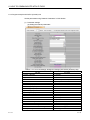
Manuals
The manuals related to this product include the following.
Direct any inquiries to your local sales store, Mitsubishi Electric Engineering service
office, or any Mitsubishi Electric product dealer, as necessary.
Detailed manuals
Included manual
Manual Title
ELC2-V680D1 RFID Interface Module User's Manual (Hardware)
Manual Number
50CM-D180159
Mitsubishi Electric Engineering CC-Link master/local interface board manuals
Manual Title
Manual Number
ECP-CL2BD Compact PCI Compatible CC-Link Interface Board User's Manual (Hardware)
50CM-D180011
ECP-CL2BD Compact PCI Compatible CC-Link Interface Board User's Manual
(Driver and Utility Software Package ECP-CL2CUTW Compatible)
50CM-D180001
Mitsubishi Electric CPU module manuals
Manual Title
QCPU User's Manual (Hardware Design, Maintenance, and Inspection)
MELSEC-L CPU Module User's Manual (Hardware Design, Maintenance, and Inspection)
Type A1N/A2N (S1) /A3NCPU User's Manual
Type A2U (S1) /A3U/A4UCPU User's Manual
Type A2A (S1) /A3ACPU User's Manual
Type A2USHCPU-S1/A2USCPU (S1)/A2ASCPU (S1/S30) User's Manual (Advanced)
Type A2USCPU (S1) User's Manual
Type A1S/A1SC24-R2/A2SCPU (S1) User's Manual
Type A1SJCPU (S3) User's Manual
Type A1SJH (S8)/A1SH/A2SHCPU (S1) User's Manual (Advanced)
A0J2HCPU (P21/R21) User's Manual
Q2ACPU (S1) /Q3ACPU/Q4ACPU User's Manual
Model Q2AS (H) CPU (S1) User's Manual
A-9
Manual Number
(Model Code)
SH-080483ENG
(13JR73)
SH-080890ENG
(13JZ36)
IB-66543
(13JE83)
IB-66436
(13JE25)
IB-66544
(13JE84)
IB-66789
(13JL30)
IB-66536
(13JE78)
IB-66320
(13J672)
IB-66446
(13J791)
IB-66779
(13JL22)
IB-66268
(13J788)
IB-66608
(13J821)
SH-3599
(13J858)
A-9
Manual Title
FX3G SERIES USER’S MANUAL - Hardware Edition
FX3U SERIES USER’S MANUAL - Hardware Edition
FX3GC SERIES USER’S MANUAL - Hardware Edition
FX3UC SERIES USER’S MANUAL - Hardware Edition
Manual Number
(Model Code)
JY997D31301
(09R521)
JY997D16501
(09R516)
JY997D45401
(09R533)
JY997D28701
(09R519)
Mitsubishi Electric CC-Link master/local module manuals
Manual Title
CC-Link System Master/Local Module Type AJ61BT11/A1SJ61BT11 User's Manual
CC-Link System Master/Local Module Type AJ61QBT11/A1SJ61QBT11 User's Manual
Type AnSHCPU/AnACPU/AnUCPU/QCPU-A (A Mode) Programming Manual (Dedicated Instructions)
MELSEC-Q CC-Link System Master/Local Module User's Manual
MELSEC-L CC-Link System Master/Local Module User's Manual
FX3U-16CCL-M USER’S MANUAL
Type Q80BD-J61BT11N/Q81BD-J61BT11 CC-Link System Master/Local Interface Board User's Manual
(For SW1DNC-CCBD2-B)
A - 10
Manual Number
(Model Code)
IB-66721
(13J872)
IB-66722
(13J873)
IB-66251
(13J742)
SH-080394E
(13JR64)
SH-080895ENG
(13JZ41)
JY997D43601
(09R724)
SH-080527ENG
(13JR77)
A - 10
Generic Terms and Abbreviations
This manual uses the following generic terms and abbreviations in product
explanations, unless otherwise specified.
Generic Term / Abbreviation
Description
RFID interface module
A generic term for an ECL2-V680D1 CC-Link OMRON V680 series compatible RFID
interface module.
V680 series
A generic term for the OMRON RFID system V680 series.
Amplifier
Antenna
An amplifier section connected to the RFID interface module for performing non-contact
communication.
An antenna section connected to the RFID interface module for performing non-contact
communication.
ID tag
A generic term for the responder side of non-contact communication.
UID
A unique number for identifying the ID tag.
GX Developer
GX Works2
Programming tool
ACPU
QnACPU
QCPU (A mode)
QCPU (Q mode)
LCPU
A product name for a MELSEC programmable controller software package.
A generic term for GX Works2 and GX Developer.
A generic term for A0J2HCPU, A1CPU, A2CPU, A2CPU-S1, A3CPU, A1SCPU,
A1SCPUC24-R2, A1SHCPU, A1SJCPU, A1SJCPU-S3, A1SJHCPU, A1NCPU, A2NCPU,
A2NCPU-S1, A3NCPU, A2SCPU, A2SHCPU, A2ACPU, A2ACPU-S1, A3ACPU, A2UCPU,
A2UCPU-S1, A2USCPU, A2USCPU-S1, A2USHCPU-S1, A3UCPU, and A4UCPU.
A generic term for Q2ACPU, Q2ACPU-S1, Q2ASCPU, Q2ASCPU-S1, Q2ASHCPU,
Q2ASHCPU-S1, Q3ACPU, and Q4ACPU.
A generic term for Q02CPU-A, Q02HCPU-A, and Q06HCPU-A.
A generic term for Q00JCPU, Q00CPU, Q01CPU, Q02CPU, Q02HCPU, Q06HCPU,
Q12HCPU, Q25HCPU, Q02PHCPU, Q06PHCPU, Q12PHCPU, Q25PHCPU, Q12PRHCPU,
Q25PRHCPU, Q00UJCPU, Q00UCPU, Q01UCPU, Q02UCPU, Q03UDCPU, Q04UDHCPU,
Q06UDHCPU, Q10UDHCPU, Q13UDHCPU, Q20UDHCPU, Q26UDHCPU, Q03UDECPU,
Q04UDEHCPU, Q06UDEHCPU, Q10UDEHCPU, Q13UDEHCPU, Q20UDEHCPU,
Q26UDEHCPU, Q50UDEHCPU, Q100UDEHCPU, Q03UDVCPU, Q04UDVCPU,
Q04UDPVCPU, Q06UDVCPU, Q06UDPVCPU, Q13UDVCPU, Q13UDPVCPU,
Q26UDVCPU, and Q26UDPVCPU.
A generic term for L02SCPU, L02SCPU-P, L02CPU, L02CPU-P, L06CPU, L06CPU-P,
L26CPU, L26CPU-P, L26CPU-BT, and L26CPU-PBT.
Master station
A station that controls the data link system. One required per system.
Local station
A station that has a CPU module and can communicate with the master station and other
local stations.
Remote I/O station
A station that handles bit data only (performs input/output with external devices).
Remote device station
A station that handles bit data and word data (performs input/output with external devices and
analog data conversion).
Remote station
A generic term for a remote I/O station and a remote device station.
Intelligent device station
A station that can perform transient transmission. (Including local stations)
Master module
A generic term for a module that can be used as a master station.
A - 11
A - 11
Generic Term / Abbreviation
Description
Link special relay (for CC-Link).
Bit data that indicates the master/local station module operating status and data link status.
Link special register (for CC-Link).
16-bit data that indicates the master/local station module operating status and data link status.
Remote input (for CC-Link)
Data input in bits from a remote station to the master station.
Remote output (for CC-Link)
Data output in bits from the master station to a remote station.
Remote register (CC-Link write area)
Data output in 16 bits from the master station to a remote device station.
Remote register (CC-link read area)
Data input in 16 bits from a remote device station to the master station.
SB
SW
RX
RY
RWw
RWr
Product Portfolio
The following indicates the product portfolio of this product.
Model
ECL2-V680D1
Product Name
ECL2-V680D1 RFID interface module
1
User’s Manual (Hardware) (Included with module)
1
Ferrite core (Included with module)
1
Crimp terminals (Red) (Included with module)
[compatible wire size : 0.3 to 1.25mm2(AWG20 to 16)]
Crimp terminals (Blue) (Included with module)
[compatible wire size : 1.25 to 2.0mm2(AWG16 to 14)]
A - 12
Quantity
13
13
A - 12
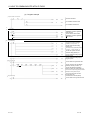
1. OVERVIEW
Chapter 1 OVERVIEW
This user’s manual describes the specifications, use, programming method, and other
information related to the ECL2-V680D1 RFID interface module used as a remote
device station of a CC-Link system.
The RFID interface module connects to the CC-Link master station of a Mitsubishi
general-purpose programmable controller (MELSEC-Q series, MELSEC-L series,
MELSEC-F series, MELSEC-AnS/QnAS series, and MELSEC-A/QnA series), enabling
reading and writing with OMRON RFID system V680 series ID tags as a remote device
station of a CC-Link system.
When utilizing the program examples introduced in this manual in an actual system, be
sure to fully verify that use will not be problematic in the control of the target system.
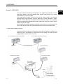
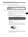
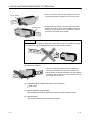
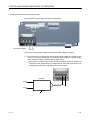
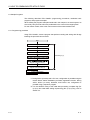
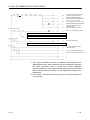
1.1 RFID Interface Module Overview
The RFID interface module has a channel that connects to a V680 series antenna, and
fulfills the role as an interface for V680 series ID tag reading and writing and the
programmable controller CPU via CC-Link.
CC-Link master/local module (master station)
Terminating
resistor
CC-Link master/local module (local station)
CC-Link dedicated cable
(Remote I/O station)
(Remote device station)
(Intelligent device station)
Terminating
resistor
ECL2-V680D1
(Remote device station)
ID tag
Antenna
Data reading and
writing with ID tag
by electromagnetic
induction (non-contact)
Amplifier
1-1
1-1
1
1. OVERVIEW
1.2 RFID Interface Module Features
1
The following describes the features of the RFID interface module.
(1) The RFID interface module enables OMRON RFID system V680 series connection
to CC-Link.
This product can connect the OMRON RFID system V680 series to CC-Link,
achieving distributed control at the distance up to 1200 m (at the 156-kbps
transmission speed). Furthermore, it is possible to construct an RFID sensor
system architecture that uses a rich group of CC-Link products.
(2) The module can read and write a maximum of 122 bytes*1 of data at one time.
*1. In the case of remote net Ver.2 mode, two occupied stations, and an octuple
expanded cyclic setting.
(3) The module permits usage of both OMRON RFID system V680 series separate-type
and amplifier built-in type antennas.
(4) The module is provided with various test functions as standard.
The communication test function allows you to check whether or not communication
with an ID tag is possible without operating the sequence program.
The distance level measurement function measures the distance (level) between
the antenna and ID tag with respect to the communication area. The function
allows you to check the measurement results in seven stages, 00 to 06.
The noise level measurement function measures the noise level in the area
surrounding the antenna installation location.
(5) The module allows you to select a mode in accordance with a variety of systems.
Remote net Ver.2 mode: Select this mode when you want to construct a new
system. The mode allows you to combine the module with an applicable master
module and increase the number of connected remote device stations to 42,
maximum.
Remote net Ver.1 mode: This mode is fully compatible with conventional remote
network modes. Select this mode when system expansion is not required.
Remote net additional mode: Select this mode when you want to add a version 2
compatible slave station to the conventional version 1 system.
(6) The module allows you to simply develop programs by downloading an FB (function
block) library that can be used with Mitsubishi Electric MELSOFT GX Works2 from
the Mitsubishi Electric Corporation FA site and FA related product site (MEEFAN).
(Supported by GX Works2 Japanese version only)
(7) The Mitsubishi Electric iQ Sensor Solution (iQSS) makes it possible to further
strengthen the linkage with the programmable controller, graphic operation terminal,
and engineering software, and achieve simple startup, sensor monitoring, and
simple programming.
(Supported by GX Works2 Japanese version only)
1-2
1-2
2. SYSTEM CONFIGURATION
Chapter 2 SYSTEM CONFIGURATION
The following describes the system configuration of the RFID interface module.
2.1 Application System
2
The following describes the application system.
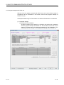
(1) Applicable combinations
The following master module, GX Works2 network parameter mode setting / station
information (station type), and module mode switch setting combinations can be
used.
Table 2.1 Application System
○: Applicable ×: Not applicable
GX Works2 Network Parameter Setting
Master Module
QJ61BT11
AJ61BT11
A1SJ61BT11
AJ61QBT11
A1SJ61QBT11
QJ61BT11N
L26CPU-BT
LJ61BT11
FX3U-16CCL-M
ECP-CL2BD
Q81BD-J61BT11
Q80BD-J61BT11N
RFID Interface Module Mode Switch Setting*1
5, 6, 7
0, 4
(Version 2 Remote
(Version 1 Remote
Device Station)
Device Station)
(Version 1 Compatible (Version 2 Compatible
Slave Station)
Slave Station)
Mode Setting
Station Information
(Station Type)
Remote net Ver.1
mode
Remote device station
○
×
Remote net Ver.1
mode
Remote device station
○
×
Version 1 remote
device station
Version 1 remote
device station
Version 1 remote
device station
Version 1 remote
device station
○
×
×
○
○*2
×
×
○*3
Remote net Ver.2
mode
Remote net additional
mode
*1. For details, refer to Section 4.5.
*2. If there is a station number that is used as a version 2 remote device station
in the existing system, set the station number of the version 1 remote
device station to be added before this station.
*3. Set the station number of the version 2 remote device station to be added
after the station number used in the existing system.
2-1
2-1
2. SYSTEM CONFIGURATION
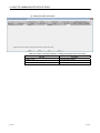
2.2 Verifying the Version
The following describes the method used to verify the version of the RFID interface
module.
2
S/W version
H/W version (circuit board)
Manufactured month
(01 to 12)
Last two digits of
manufactured year
Example: When manufactured in September 2014 and both the
hardware and software versions are "B":
1409BB
Indicates the year and month.
Example: 2014‐09 2-2
2-2
2. SYSTEM CONFIGURATION
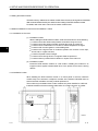
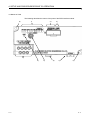
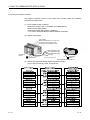
2.3 Overall Configuration
The following indicates the overall configuration of the RFID system.
The antennas, amplifier and ID tags can be used in certain combinations. Refer to the
OMRON RFID system V680 series catalog.
Q series
L series
FX series
AnS/QnAS A/QnA
CC-Link master module
CC-Link cable
24V DC external
power supply
RFID interface module
Amplifier
Extension cable
Extension cable
Amplifier built-in type antenna
Antennas
ID tags
2-3
2-3
2. SYSTEM CONFIGURATION
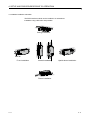
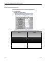
2.4 Component List
The component lists the required equipment for using the RFID interface module.
Table 2.2 Component List
Product Name
RFID interface module
Amplifier
Antenna
(separate amplifier
type)
Antenna
(amplifier built-in type)
EEPROM type ID tag
FRAM type ID tag
2-4
Model
ECL2-V680D1
Remarks
V680 series RFID interface module; one antenna connected
V680-HA63A
For EEPROM type ID tags (V680-D1KP□□)
V680-HA63B
For FRAM type ID tags (V680-D2KF□□/V680-D8KF□□/V680-D32KF□□)
V680-HS51
For ID tag communication; Φ18mm type; cable length: 2m/12.5m
V680-HS52
For ID tag communication; Φ22mm type; cable length: 2m/12.5m
V680-HS63
For ID tag communication; 40x53mm type; cable length: 2m/12.5m
V680-HS65
For ID tag communication; 100x100mm type; cable length: 2m/12.5m
V680-H01-V2
For ID tag communication; 250x200mm type; cable length: 0.5m
V680-D1KP52MT
Memory capacity: 1kbyte (1,000 bytes); Φ8mm type; metal embedding permitted
V680-D1KP53M
Memory capacity: 1kbyte (1,000 bytes); Φ10mm type; metal embedding permitted
V680-D1KP54T
Memory capacity: 1kbyte (1,000 bytes); Φ20mm type
V680-D1KP66MT
Memory capacity: 1kbyte (1,000 bytes); 34x34mm type; metal embedding permitted
V680-D1KP66T
Memory capacity: 1kbyte (1,000 bytes); 34x34mm type
V680-D1KP66T-SP
Memory capacity: 1kbyte (1,000 bytes); oil-proof and chemical resistant specifications
V680-D1KP58HTN
Memory capacity: 1kbyte (1,000 bytes); Φ80mm type; heat resistant specifications
V680-D1KP52M-BT01
Memory capacity: 1kbyte (1,000 bytes); M10 bolt installation
V680-D1KP52M-BT11
Memory capacity: 1kbyte (1,000 bytes); M8 bolt installation
V680-D2KF52M
Memory capacity: 2kbytes (2,000 bytes); Φ8mm type; metal embedding permitted
V680-D2KF67M
Memory capacity: 2kbytes (2,000 bytes); 40x40mm type; metal installation permitted
V680-D2KF67
Memory capacity: 2kbytes (2,000 bytes); 40x40mm type
V680S-D2KF67M
Memory capacity: 2kbytes (2,000 bytes); 40x40mm type; metal installation permitted
V680S-D2KF67
Memory capacity: 2kbytes (2,000 bytes); 40x40mm type
V680S-D2KF68M
Memory capacity: 2kbytes (2,000 bytes); 86x54mm type; metal installation permitted
V680S-D2KF68
Memory capacity: 2kbytes (2,000 bytes); 86x54mm type
V680-D2KF52M-BT01
Memory capacity: 2kbytes (2,000 bytes); M10 bolt installation
V680-D2KF52M-BT11
Memory capacity: 2kbytes (2,000 bytes); M8 bolt installation
V680-D8KF67M
Memory capacity: 8kbytes (8,192 bytes); 40x40mm type; metal installation permitted
V680-D8KF67
Memory capacity: 8kbytes (8,192 bytes); 40x40mm type
V680S-D8KF67M
Memory capacity: 8kbytes (8,192 bytes); 40x40mm type; metal installation permitted
V680S-D8KF67
Memory capacity: 8kbytes (8,192 bytes); 40x40mm type
V680-D8KF68
Memory capacity: 8kbytes (8,192 bytes); 86x54mm type
V680S-D8KF68M
Memory capacity: 8kbytes (8,192 bytes); 86x54mm type; metal installation permitted
V680S-D8KF68
Memory capacity: 8kbytes (8,192 bytes); 86x54mm type
V680-D32KF68
Memory capacity: 32kbytes (32,744 bytes); 86x54mm type
2-4
2. SYSTEM CONFIGURATION
Product Name
Extension cable
Model
Remarks
V700-A40
For amplifier V680-HA63A/63B connection; cable length: 2m
V700-A41
For amplifier V680-HA63A/63B connection; cable length: 3m
V700-A42
For amplifier V680-HA63A/63B connection; cable length: 5m
V700-A43
For amplifier V680-HA63A/63B connection; cable length: 10m
V700-A44
For amplifier V680-HA63A/63B connection; cable length: 20m
V700-A45
For amplifier V680-HA63A/63B connection; cable length: 30m
V700-A40-W
For amplifier built-in type antenna V680-H01-V2 connection; cable length:
cable length: 2m/5m/10m/20m/30m
* Configurations as of October 2014. For the latest V680 series configurations and
amplifier, antenna, and ID tag combinations, refer to the OMRON RFID system V680
series catalog.
* For V680S-D8KF□□, use an RFID interface module of S/W version B or later as stated
on the rating nameplate. For information on how to verify the S/W number, refer to
Section 2.2.
2-5
2-5
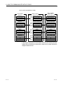
3. SPECIFICATIONS
Chapter 3 SPECIFICATIONS
The following describes the RFID interface module general specifications, performance
specifications, remote Input/Output signals and remote register specification for the
master module.
3.1 General Specifications
Table 3.1 General Specifications
Item
3
Specifications
Operating ambient temperature
0 to 55˚C
Storage ambient temperature
-20 to 75˚C
Operating ambient humidity
10 to 90% RH, non-condensing
Storage ambient humidity
10 to 90% RH, non-condensing
Frequency
JIS B 3502
and
IEC 61131-2
compliant
Vibration resistance
With
intermittent
vibration
With
continual
vibration
Acceleration Amplitude
5 to 8.4Hz
-
3.5mm
8.4 to 150Hz
9.8m/s2
-
5 to 8.4Hz
-
1.75mm
8.4 to 150Hz
4.9m/s2
-
Sweep
Count
10 times
each in X, Y,
Z directions
-
JIS B 3502 and IEC 61131-2 compliant
Impact resistance
(147m/s2; 3 times each in X, Y, and Z directions)
Operating environment
Operating altitude*1
Free of corrosive gasses
0 to 2000m
Installation location
Inside control panel
*2
Overvoltage category
II
Pollution degree*3
2
*1. Do not operate the programmable controller at an altitude of 0m or greater in a
pressurized environment. Doing so results in the risk of malfunction
*2. This indicates the section of the power supply to which the equipment is
assumed to be connected between the public electrical power distribution
network and the machinery within the premises. Category II applies to equipment
for which electrical power is supplied from fixed facilities. The surge voltage
withstand level for up to the rated voltage of 300V is 2500V.
*3. This index indicates the degree to which conductive material is generated in
terms of the environment in which the equipment is used. Pollution level 2 is
when only non-conductive pollution occurs. A temporary conductivity caused by
condensing must be expected occasionally.
3-1
3-1
3. SPECIFICATIONS
3.2 Performance Specifications
The following describes the performance specifications of the RFID interface module.
Table 3.1 Performance Specifications
Item
RFID
side
Connectable antenna
Number of connectable
antennas
CC-Link station type
CC-Link version
Station number selections
Transmission speed
CC-Link
side
Number of occupied stations
and data transfer volume
Connection cable
External power supply
Noise resistance
Withstand voltage
Insulation resistance
Outer dimensions
Weight
External
Communication area,
connection
module power supply area
method
Module installation screws
Applicable DIN rail
Applicable crimp terminals
Applicable Compression tools for wire
connectors
Specifications
V680-HA63A+V680-HS□□
V680-HA63B+V680-HS□□
V680-H01-V2
1 antenna
Remote device station
Ver. 1.10 and Ver. 2.0
With 2 occupied stations: Station numbers 1 to 63
With 4 occupied stations: Station numbers 1 to 61
156kbps/625kbps/2.5Mbps/5Mbps/10Mbps (selectable)
Amount of data
Number of
CC-Link
Expanded
Data transfer
readable/writable with
occupied
*1
version
cyclic setting
volume
one ID command
stations
2 occupied
8 words
10 bytes
stations
Ver.1.10
4 occupied
16 words
26 bytes
stations
Double
16 words
26 bytes
2 occupied
Ver.2.0
Quadruple
32 words
58 bytes
stations
Octuple
64 words
122 bytes
Ver. 1.10 compatible CC-Link dedicated cable
CC-Link dedicated cable (Ver. 1.00 compatible)
CC-Link dedicated high performance cable (Ver. 1.00 compatible)
24V DC (20.4 to 26.4V DC) (ripple rate: within 5%)
Current consumption: 0.33A
DC-type noise voltage 500Vp-p, noise width 1μs, based on a noise simulator with
a noise frequency of 25 to 60Hz
All DC external terminals – Ground: 500V AC, 1 minute
All DC external terminals – Ground: 500V DC,
10MΩ using insulation resistance tester
65(H)X150(W)X45(D)[mm]
0.3kg
7-point 2-piece terminal block [transmission circuit, module power supply, FG]
M3 x 5.2 screws (tightening torque range: 4.70 to 5.22in•lbs (0.54 to 0.59N•m)
Number of inserted compatible crimp terminals: 2 or less
M4 screw with plain washer finished round
(tightening torque range: 0.79 to 1.08N•m)
DIN rail installable, installable in 6 directions
TH35-7.5Fe, TH35-7.5Al (JIS C 2812 compliant)
• N1.25-3 (JST Mfg. Co., Ltd.)
[compatible wire size : 0.3 to 1.25mm2(AWG20 to 16)]
• N2-MS3 (JST Mfg. Co., Ltd.)
2
[compatible wire size : 1.25 to 2.0mm (AWG16 to 14)]
• YNT-2216 (JST Mfg. Co., Ltd.),
T-212 (Nippon Tanshi Co., Ltd.),
NH11 (Nichifu Co., Ltd.)
2
[compatible wire size : 0.3 to 1.25mm (AWG20 to 16)]
• YNT-1614 (JST Mfg. Co., Ltd.),
T-221N (Nippon Tanshi Co., Ltd.),
NH12 (Nichifu Co., Ltd.)
2
[compatible wire size : 1.25 to 2.0mm (AWG16 to 14)]
*1. The value includes the command code specification area, etc., as well.
3-2
3-2
3
3. SPECIFICATIONS
Point
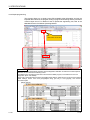
Each of the following conditions must be satisfied:
(1)
In remote net Ver.1 mode
Condition 1
{(1×a) + (2×b) + (3×c) + (4×d)} ≤ 64
a: Number of modules with one occupied station
b: Number of modules with two occupied stations
c: Number of modules with three occupied stations
d: Number of modules with four occupied stations
Condition 2
{(16×A) + (54×B) + (88×C)} ≤ 2304
A: Number of remote I/O stations ≤ 64 stations
B: Number of remote device stations ≤ 42 stations
C: Number of local stations, standby master stations, and intelligent device stations ≤ 26 stations
(2)
In remote net Ver.2 mode and remote net additional mode
Condition 1
{(a + a2 + a4 + a8) + (b + b2 + b4 + b8) ×2 + (c + c2 +c4 + c8) ×3+ (d + d2 + d4 + d8) ×4}
≤ 64
Condition 2
[{(a×32) + (a2×32) + (a4×64) + (a8×128)} + {(b×64) + (b2×96) + (b4×192) + (b8×384)}
+ {(c×96) + (c2×160) + (c4×320) + (c8×640)} + {(d×128) + (d2×224) + (d4×448) + (d8×896)}]
≤ 8192
Condition 3
[{(a×4) + (a2×8) + (a4×16) + (a8×32)} + {(b×8) + (b2×16) + (b4×32) + (b8×64)}
+ {(c×12) + (c2×24) + (c4×48) + (c8×96)} + {(d×16) + (d2×32) + (d4×64) + (d8×128)}] ≤ 2048
a: Total number of Ver. 1 compatible slave stations with one occupied station and Ver. 2
compatible slave stations with one occupied station set to “Single”
b: Total number of Ver. 1 compatible slave stations with two occupied stations and Ver. 2
compatible slave stations with two occupied stations set to “Single”
c: Total number of Ver. 1 compatible slave stations with three occupied stations and Ver. 2
compatible slave stations with three occupied stations set to “Single”
d: Total number of Ver. 1 compatible slave stations with four occupied station and Ver. 2
compatible slave stations with four occupied stations set to “Single”
a2: Total number Ver. 2 compatible slave stations with one occupied station set to “Double”
b2: Total number Ver. 2 compatible slave stations with two occupied stations set to “Double”
c2: Total number Ver. 2 compatible slave stations with three occupied stations set to “Double”
d2: Total number Ver. 2 compatible slave stations with four occupied stations set to “Double”
a4: Total number Ver. 2 compatible slave stations with one occupied station set to “Quadruple”
b4: Total number Ver. 2 compatible slave stations with two occupied stations set to “Quadruple”
c4: Total number Ver. 2 compatible slave stations with three occupied stations set to “Quadruple”
d4: Total number Ver. 2 compatible slave stations with four occupied stations set to “Quadruple”
a8: Total number Ver. 2 compatible slave stations with one occupied station set to “Octuple”
b8: Total number Ver. 2 compatible slave stations with two occupied stations set to “Octuple”
c8: Total number Ver. 2 compatible slave stations with three occupied stations set to “Octuple”
d8: Total number Ver. 2 compatible slave stations with four occupied stations set to “Octuple”
Condition 4
{(16×A) + (54×B) + (88×C)} ≤ 2304
A: Number of remote I/O stations ≤ 64 stations
B: Number of remote device stations ≤ 42 stations
C: Number of local stations, standby master stations, and intelligent device stations ≤ 26 stations
3-3
3-3
3. SPECIFICATIONS
3.3 Functions
The RFID interface module has two operation modes: RUN mode and TEST mode.
The following describes the functions of each mode.
3.3.1 RUN mode
RUN mode is used during programmable controller operation.
Table 3.3 RUN Mode Functions List
Function
Read
Command
Reference
Read
Reads data from an ID tag.
Section 6.2.1
Read UID
Reads the UID (unit identification number) of an ID tag.
Section 6.2.4
Reads the Initial Data Settings.
Section 6.2.6
Writes data to an ID tag.*1
Section 6.2.2
Read Initial Data
Settings
Write
Description
Write
Initialize
Fill Data
Initializes data of an ID tag with specified data.
Section 6.2.3
Management
Measure Noise
Measures the noise environment around an antenna.
Section 6.2.5
*1. Not compatible with data handled by Read with Error Correction, Write with Error
Correction, or Data Check of the EQ-V680D1/EQ-V680D2 RFID interface module.
3.3.2 TEST mode
TEST mode is used when set up the RFID system or when performing maintenance.
To set the mode to TEST mode, either set the mode switch located on the front of the
RFID interface module to TEST mode or set the test mode execution request (RYn5) to
ON in the sequence program.
Table 3.4 TEST Mode Functions List
Function
Description
Reference
Reads data from the ID tag.
Communication test Checks whether a sequence program, antenna, or ID tag caused a read error Section 5.1.3(2)
when a data read error occurs with an ID tag.
Distance level
measurement
Checks the margin with respect to the maximum communication distance
(potential) of the installation distance of the ID tag.
Noise level
Checks whether noise that adversely affects communication with an ID tag is
measurement
occurring in the area surrounding the antenna installation location.
3-4
Section 5.1.3(3)
Use this function to adjust the installation location.
Section 5.1.3(4)
3-4
3. SPECIFICATIONS
3.4 Remote I/O Signals
3.4.1 Remote I/O signal list
The following provides a list of the remote I/O signals of the RFID interface module.
Remote input (RX) refers to an input signal from the RFID interface module to the
master module, and remote output (RY) refers to an output signal from the master
module to the RFID interface module.
Table 3.5 Remote I/O Signal List
Signal Direction: RFID Interface Module → Master Module
Remote Input (RX)
Signal Name
RXn0
Signal Direction: Master Module → RFID Interface Module
Remote Output (RY)
Signal Name
RYn0 to RYn3
Use prohibited
Use prohibited
RXn1
RXn2
ID communication complete
RXn3
ID-BUSY
RXn4
ID command complete
RYn4
ID command execution request
RXn5
Error detection
RYn5
TEST mode execution request
*1
RXn6 to RX(n+k)7
Use prohibited
RYn6
Result reception
*1
RYn7 to RY(n+k)7
*1
Initial data processing request flag
RY(n+k)8
*1
Initial data setting complete flag
RY(n+k)9
*1
Use prohibited
RY(n+k)A
*1
Remote READY
RX(n+k)8
RX(n+k)9
RX(n+k)A
RX(n+k)B
*1
RX(n+k)C to RX(n+k)F
Use prohibited
Use prohibited
*1
Initial data processing complete flag
*1
Initial data setting request flag
*1
Use prohibited
*1
Use prohibited
RY(n+k)B to RY(n+k)F
n: Address assigned to master station by station number setting.
*1
k: Address assigned by set value of mode switch.
Point
Use-prohibited I/O signals are used by the system and cannot be used by users. In the
unlikely event that a use-prohibited I/O signal is turned ON/OFF by a sequence program, the
functions of the RFID interface module cannot be guaranteed.
*1. k of remote input (RX) and remote output (RY) is as follows according to the
mode switch setting.
Table 3.6 Remote I/O Signal Range
Mode Switch
Set Value
k
Remote Input (RX)
Remote Output (RY)
Start
End
Start
End
7
RXn0
RX(n+7)F
RYn0
RY(n+7)F
4
3
RXn0
RX(n+3)F
RYn0
RY(n+3)F
5
5
RXn0
RX(n+5)F
RYn0
RY(n+5)F
6
B
RXn0
RX(n+B)F
RYn0
RY(n+B)F
7
17
RXn0
RX(n+17)F
RYn0
RY(n+17)F
0
Remarks
Ver. 1 compatible, 4 occupied stations
RX/RY: 128 points each
1
2
3
Ver. 1 compatible, 2 occupied stations
RX/RY: 64 points each
Ver. 2 compatible, 2 occupied stations
Expanded cyclic setting: Double
RX/RY: 96 points each
Ver. 2 compatible, 2 occupied stations
Expanded cyclic setting: Quadruple
RX/RY: 192 points each
Ver. 2 compatible, 2 occupied stations
Expanded cyclic setting: Octuple
RX/RY: 384 points each
n: Address assigned to master station by station number setting.
3-5
3-5
3. SPECIFICATIONS
3.4.2 Remote I/O signal details
The following describes in detail the remote I/O signals of the RFID interface module.
(1) Remote input signals
Table 3.7 Remote Input Signal Details
Device No.
Signal Name
Description
This signal is used only when the communication specification is repeat auto or FIFO repeat.
(1) Turns ON when result reception (RYn6) turns ON/OFF by turning ON of error detection
(RXn5) when ECL2-V680D1 suspends communication due to the elapse of the auto
system command wait time.
(2) Turns ON when result reception (RYn6) turns ON/OFF by turning ON of error detection
(RXn5) when communication is suspended due to antenna disconnection.
(3) Turns OFF when the ID command execution request (RYn4) is turned OFF and
received by ECL2-V680D1.
(4) The timing chart is as follows:
1) Error detection (RXn5) turns ON when ECL2-V680D1 suspends communication due
to the elapse of the auto system command wait time or antenna disconnection.
2) ID communication complete (RXn2) turns ON when result reception (RYn6) turns
ON/OFF.
3) The ID command execution request (RYn4) turns OFF when ID communication
complete (RXn2) turns ON.
4) ID communication complete (RXn2) and ID-BUSY (RXn3) turn OFF when the ID
command execution request (RYn4) is turned OFF.
RXn2
ID communication
ID command
execution request
(RYn4)
complete
Error detection
(RXn5)
Result reception
(RYn6)
ID communication
complete(RXn2)
ID-BUSY(RXn3)
1)
2)
3)
4)
Implemented by ECL2-V680D1
Implemented by sequence program
(1)
RXn3
ID-BUSY
(2)
(3)
(4)
3-6
Turns ON when the ID command execution request (RYn4) is turned ON and received
by the RFID interface module.
Turns OFF when the ID command execution request (RYn4) is turned OFF and received
by the RFID interface module.
Always ON in TEST mode.
For the timing chart, refer to "ID command complete (RXn4)".
3-6
3. SPECIFICATIONS
Device No.
Signal Name
Description
(1)
(2)
(3)
Turns ON when the ID command execution request (RYn4) is turned ON and the status
is normal upon ID command execution completion. Error detection (RXn5) turns ON
when the status is abnormal upon ID command execution completion.
Turns OFF when the ID command execution request (RYn4) is turned OFF and received
by the RFID interface module.
The timing chart is as follows:
1) The ID command execution contents are set in the remote register (RWw).
2) ID-BUSY (RXn3) turns ON when the ID command execution request (RYn4) turns ON,
and the ID command is executed in accordance with the set contents of step 1 above.
3) ID command complete (RXn4) turns ON when the status is normal upon ID command
execution completion.
4) ID-BUSY (RXn3) and ID command complete (RXn4) turn OFF when the ID command
execution request (RYn4) is turned OFF.
Implemented by RFID interface module
RXn4
ID command complete
Implemented by sequence program
Remote register
(RWw)
ID command
execution request
(RYn4)
ID-BUSY (RXn3)
ID command execution
ID command
complete (RXn4)
1) 2)
3) 4)
[RUN mode]
(1) Turns ON when the ID command execution request (RYn4) is turned ON and the ID
command ends abnormally.
(2) Turns OFF when the ID command execution request (RYn4) is turned OFF and
received by the RFID interface module.
(3) ID command complete (RXn4) does not turn ON when the ID command ends
abnormally.
Implemented by RFID interface module
Implemented by sequence program
Clear Error command
RXn5
Error detection
ID command
execution request
(RYn4)
ID-BUSY (RXn3)
ID command
complete(RXn4)
Error detection
(RXn5)
Error details
(RWrm+1H)
0
Error details
Error occurrence
3-7
0
Clear Error execution
3-7
3. SPECIFICATIONS
Device No.
Signal Name
Description
[Initial data setting]
(1)
Turns ON after storage of error details in error details (RWrn+1H) when the initial data
setting request flag (RY(n+k)9) is turned ON and an out-of-range value is specified in
the communication specification area (RWwm+0H) or the processing specification area
(RWwm+2H).
(2)
Turns OFF when the initial data setting request flag (RY(n+k)9) is turned OFF and
received by the RFID interface module.
(3)
The initial data setting complete flag (RX(n+k)9) turns ON even if initial data setup ends
abnormally.
(4)
Does not turn ON when a watchdog timer error occurs. (The "RUN" LED turns off.)
Implemented by RFID interface module
Implemented by sequence program
RXn5
Clear Error command
Error detection
Initial data setting request flag
(RY(n+k)9)
Initial data setting complete flag
(RX(n+k)9)
Error detection (RXn5)
Error details(RWrn+1H)
0
Error details
Error occurrence
(1)
0
Clear Error execution
Turns ON after power ON or reset for a request for initial data setup by the RFID
interface module.
(2)
Turns OFF when the initial data processing complete flag (RY(n+k)8) is turned ON and
received by the RFID interface module.
Implemented by RFID interface module
Implemented by sequence program
Initial data processing
request flag(RX(n+k)8)
RX(n+k)8
Initial data processing
request flag
Initial data processing
complete flag(RY(n+k)8)
Initial data setting complete
flag(RX(n+k)9)
Initial data setting request
flag(RY(n+k)9)
Initialization execution
Remote register(RWw)
Remote READY(RX(n+k)B)
3-8
3-8
3. SPECIFICATIONS
Device No.
Signal Name
Description
(1)
RX(n+k)9
Initial data setting
complete flag
Turns ON after initial data setting completion when the initial data setting request flag
(RY(n+k)9) is turned ON.
(2)
Turns OFF when the initial data setting request flag (RY(n+k)9) is turned OFF and
received by the RFID interface module.
(3)
(1)
For the timing chart, refer to "Initial data processing request flag (RX(n+k)8)".
Turns ON after initial data setup is complete and the RFID interface module is ready
after power ON or reset.
(2)
Turns OFF when the initial data setting request flag (RY(n+k)9) is turned ON and
received by the RFID interface module.
(3)
Turns ON when the initial data setting request flag (RY(n+k)9) is turned OFF and
received by the RFID interface module.
(4)
Turns OFF in TEST mode.
Implemented by the RFID interface module
RX(n+k)B
Remote READY
Implemented by the sequence program
Initial data setting complete
flag(RX(n+k)9)
Initial data setting request flag
(RY(n+k)9)
Remote READY(RX(n+k)B)
n: Address assigned to master station by station number setting.
k: Address assigned by set value of mode switch.
3-9
3-9
3. SPECIFICATIONS
(2) Remote output signals
Table 3.8 Remote Output Signal Details
Device No.
RYn4
RYn5
Signal Name
ID command execution
request
TEST mode execution
request
Description
(1)
Executes the ID command of the contents set in the remote register (RWw) when the
sequence program turns ON.
(2)
For the timing chart, refer to "ID command complete (RXn4)".
(1)
Executes TEST mode when turned ON by the sequence program.
This signal is used only when the communication specification is repeat auto or FIFO repeat.
(1)
Used as a trigger signal for communication with the next ID tag when the communication
specification is repeat auto or FIFO repeat.
(2)
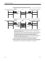
RYn6
Result reception
The timing chart is as follows:
1) The result information is acquired and result reception (RYn6) is turned ON when ID
command complete (RXn4) turns ON.
2) ID command complete (RXn4) turns OFF when result reception (RYn6) is turned
ON.
3) Result reception (RYn6) is turned OFF when ID command complete (RXn4) turns
OFF.
Implemented by RFID interface module
Implemented by sequence program
ID command
complete
(RXn4)
Result reception
(RYn6)
1)
RY(n+k)8
RY(n+k)9
Initial data processing
complete flag
Initial data setting
request flag
(1)
2)
3)
Turns ON after initial data processing is completed when there is an initial data
processing request after power ON or reset.
(2)
For the timing chart, refer to "Initial data processing request flag (RX(n+k)8)".
(1)
Turns ON when initial data is set or changed.
(2)
For the timing chart, refer to "Initial data processing request flag (RX(n+k)8)".
(3)
Not executed during ID command execution, even if the initial data setting request flag
(RY(n+k)9) is turned ON. Turn the flag ON after turning the ID command execution
request (RYn4) OFF and the ID command is completed.
(4)
Not executed in TEST mode, even if the initial data setting request flag (RY(n+k)9) is
turned ON.
n: Address assigned to master station by station number setting.
k: Address assigned by set value of mode switch.
3 - 10
3 - 10
3. SPECIFICATIONS
3.5 Remote Registers
(1) Remote register assignments of remote device stations
Table 3.9 Remote Register List
Operation Mode
Reception Direction
Description
RWwm+0H
Communication specification area
0
Section 3.6.1 (1)
RWwm+1H
Communication setting area
0
Section 3.6.1 (2)
RWwm+2H
Processing specification area
0
Section 3.6.1 (3)
RWwm+3H
Auto system command wait time setting area
0
Section 3.6.1 (4)
RWwm+4H
*1
and thereafter
Use prohibited
0
-
RWrm+0H
Module status storage area
0
Section 3.6.1 (5)
RWrm+1H
Error details storage area
0
Section 3.6.1 (6)
RWrm+2H
*1
and thereafter
Use prohibited
0
-
RWwm+0H
Command code specification area
0
Section 3.6.2 (1)
RWwm+1H
Start address specification area
0
Section 3.6.2 (2)
RWwm+2H
Number of processing points specification
area
0
Section 3.6.2 (3)
RWwm+3H
*1
and thereafter
Write data specification area 1 and
*2
thereafter
0
Section 3.6.2 (4)
RWrm+0H
Module status storage area
0
Section 3.6.2 (5)
RWrm+1H
Error details storage area
0
Section 3.6.2 (6)
RWrm+2H
Use prohibited
0
-
Master module
RWrm+3H
*1
and thereafter
Read data storage area 1 and thereafter
0
Section 3.6.2 (7)
Master module
RWwm+0H
Test operation mode specification area
0
Section 3.6.3 (1)
RFID interface module
RWwm+1H
*1
and thereafter
Use prohibited
0
-
RWrm+0H
Module status storage area
0
Section 3.6.3 (2)
Use prohibited
0
-
RWrm+3H
Processing result storage area
0
Section 3.6.3 (3)
RWrm+4H
*1
and thereafter
Use prohibited
0
-
Master module
Initial data
setting
RFID interface module
RFID interface module
Master module
Master module
RFID interface module
RUN mode
RFID interface module
TEST mode
Initial
Value
Address
RFID interface module
Master module
RWrm+1H
RWrm+2H
*2
Reference
m: Address assigned to master station by station number setting.
Point
(1) Use-prohibited devices are used by the system and cannot be used by users. In the
unlikely event that a use-prohibited device is used by a user, normal operation cannot be
guaranteed.
(2) When you want to read or write 32-bit data using the MELSEC-A series FROM/TO
instruction, do so from an even address. Reading or writing 32-bit data from an odd
address may result in 32-bit data separation.
3 - 11
3 - 11
3. SPECIFICATIONS
*1. The last address is as follows according to the mode switch setting.
Table 3.10 Remote Register Last Address
Last Address
Mode Switch Set
Value
RWw
RWr
Remarks
0
RWwm+FH
RWrm+FH
1 to 3
-
-
Ver. 1 compatible, 4 occupied stations, RWw/RWr: 16 points each
4
RWwm+7H
RWrm+7H
Ver. 1 compatible, 2 occupied stations, RWw/RWr: 8 points each
5
RWwm+FH
RWrm+FH
Ver. 2 compatible, 2 occupied stations, Expanded cyclic setting
: Double, RWw/RWr: 16 points each
6
RWwm+1FH
RWrm+1FH
Ver. 2 compatible, 2 occupied stations, Expanded cyclic setting
: Quadruple, RWw/RWr: 32 points each
7
RWwm+3FH
RWrm+3FH
Ver. 2 compatible, 2 occupied stations, Expanded cyclic setting
: Octuple, RWw/RWr: 64 points each
8 to F
-
-
-
m: Address assigned to master station by station number setting.
*2. The address and contents in RUN mode are as follows according to the mode
switch setting.
Table 3.11 Remote Register Address Range
Mode Switch Set
Value
0
1 to 3
4
Address
Description
RWwm+3H to RWwm+FH
Write data specification areas 1 to 13
RWrm+3H to RWrm+FH
Read data storage areas 1 to 13
Ver. 1 compatible, 4 occupied
stations, 13 points (26 bytes)
-
-
RWwm+3H to RWwm+7H
Write data specification areas 1 to 5
RWrm+3H to RWrm+7H
Read data storage areas 1 to 5
RWwm+3H to RWwm+FH
Write data specification areas 1 to 13
RWrm+3H to RWrm+FH
Read data storage areas 1 to 13
RWwm+3H to RWwm+1FH
Write data specification areas 1 to 29
RWrm+3H to RWrm+1FH
Read data storage areas 1 to 29
RWwm+3H to RWwm+3FH
Write data specification areas 1 to 61
RWrm+3H to RWrm+3FH
Read data storage areas 1 to 61
Ver. 2 compatible, 2 occupied
stations, Expanded cyclic setting
: Octuple, 61 points (122 bytes)
-
-
-
5
6
7
8 to F
Remarks
Ver. 1 compatible, 2 occupied
stations, 5 points (10 bytes)
Ver. 2 compatible, 2 occupied
stations, Expanded cyclic setting
: Double, 13 points (26 bytes)
Ver. 2 compatible, 2 occupied
stations, Expanded cyclic setting
: Quadruple, 29 points (58 bytes)
m: Address assigned to master station by station number setting.
3 - 12
3 - 12
3. SPECIFICATIONS
3.6 Remote Register Details
3.6.1 Initial data setting
(1) Communication specification area (RWwm+0H)
The communication specification method is selected according to the ID tag status
(stationary or moving). For details of the control method for each communication
specification, refer to Section 6.3, “Control Method by Communication Specification”.
The contents set become enabled when the initial data setting request flag (RY(n+k)9)
turns ON.
Table 3.12 Communication Specification Area
Specification
*3
Value
Name
0000H
Trigger
Description
(1)
*1
(2)
(1)
0001H
Communicates with a static ID tag located within the antenna communication area when
the ID command execution request (RYn4) turns ON.
Be sure that there is only one ID tag in the antenna communication area.
Waits for detection of an ID tag moving within the antenna communication area after the ID
command execution request (RYn4) turns ON, and then executes communication.
Auto
(2)
(1)
Be sure that there is only one ID tag in the antenna communication area.
Waits for detection of an ID tag moving within the antenna communication area after the ID
command execution request (RYn4) turns ON, and then executes communication.
0002H
Repeat auto
(2)
Does not execute communication with ID tags that stay in the communication area.
(3)
Waits again for the approach of a moving ID tag after response transmission is completed,
continually executes communication with subsequent ID tags, and stops communication
when the ID command execution request (RYn4) turns OFF.
(4)
(1)
Be sure that there is only one ID tag in the antenna communication area.
Communicates with an operable ID tag within the antenna communication area after the ID
command execution request (RYn4) turns ON.
0003H
*2
FIFO trigger
(2)
Sets the ID tag to an operation disabled state after communication completion.
(3)
Does not communicate with an ID tag with which communication was once already
performed when that same ID tag is within the communication area.
(4)
Be sure that only one operable ID tag is within the antenna communication area during ID
tag communication.
(1)
Waits for detection of an operable ID tag within the antenna communication area after the
ID command execution request (RYn4) turns ON, and then performs communication.
0004H
(2)
Sets the ID tag to an operation disabled state after communication completion.
(3)
Does not communicate with the same ID tag again when an ID tag with which
communication was once already performed is within the communication area.
*2
FIFO repeat
(4)
Be sure that only one operable ID tag is within the antenna communication area during ID
tag communication.
(5)
Waits again for the approach of a moving ID tag after response transmission completion,
continuously executes communication with subsequent ID tags, and stops communication
when the ID command execution request (RYn4) turns OFF.
*1. The value is set to trigger by default.
*2. Cannot be used for communication with V680-D1KP□□.
*3. If an out-of-range value is specified, error detection (RXn5) turns ON. The set
contents are not updated.
3 - 13
3 - 13
3. SPECIFICATIONS
(2) Communication setting area (RWwm+1H)
The communication setting area selects the communication settings shown in
Table 3.13.
The contents set become enabled when the initial data setting request flag
(RY(n+k)9) turns ON.
Table 3.13 Communication Setting Area
Bit
Name
0
Write verify setting
1
ID tag communication
*2 *5
speed setting
2
Write protect setting
3
Read/Write data code
*3
setting
4 to 15
Not used
*1
Description
Sets whether or not the write verify function, which automatically verifies that data is normally
written by the RFID interface module when a write command is executed, is to be executed.
0: Execute
1: Do not execute
Shortens the communication time when the communication time with the ID tag is long with
the standard communication speed setting.
0: Standard mode
1: High-speed mode
Enables/Disables the write protect function (ID tag write prohibit function).
0: Enable
1: Disable
Specifies the read/write data code.
0: Without ASCII/HEX conversion
1: With ASCII/HEX conversion
0: Fixed
*4
*1. The default values are set as follows:
Write verify setting
: Execute
ID tag communication speed setting : Standard mode
Write protect setting
: Enable
Read/Write data code setting
: Without ASCII/HEX conversion
*2. If FIFO trigger or FIFO repeat is specified in the communication specification area
(RWwm+0H), the communication speed is set to standard mode even if high-speed mode
is set as the ID tag communication speed setting.
3 - 14
3 - 14
3. SPECIFICATIONS
*3. The following shows examples of ASCII/HEX conversion.
1) Without ASCII/HEX conversion, Data storage order: Upper → Lower, Number of processing
points: 2
ID tag
Write data specification area 1 and thereafter
(RWwm+3H and thereafter)
Write
BA21H
Address
Read data storage area 1 and thereafter
(RWrm+3H and thereafter)
Read
0010H
BAH
0011H
21H
BA21H
2) With ASCII/HEX conversion, Data storage order: Upper → Lower, Number of processing
points: 4
If ASCII/HEX conversion is set to "With ASCII/HEX conversion," set the number of bytes
of ASCII to be read from or written to the ID tag in the number of processing points
specification area (RWwm+2H).
If ASCII/HEX conversion is set to "With ASCII/HEX conversion", reading is performed
from an ID tag, and a code not expressed in hexadecimal format exists in the conversion
source data (a value other than "0" to "9" and "A" to "F"), bit 14 of the error details
storage area (RWrm+1H) turns ON and error detection (RXn5) turns ON.
If the number of processing points specified in the number of processing points
specification area (RWwm+2H) is odd, bit 0 of the error details storage area (RWrm+1H)
turns ON and error detection (RXn5) turns ON.
ASCII/HEX conversion is enabled only with a Read/Write command. ASCII/HEX
conversion is not performed with Fill Data, Read UID, or Measure Noise.
*4. If 1 is set, error detection (RXn5) turns ON. The set contents are not updated.
*5. When the V680S-D8KF□□ ID tag is used, the communication time does not differ from the
standard mode time, even if high-speed mode is selected. For communication time details,
refer to Appendix 1 "Communication Time" and Appendix 2 "Processing Time."
3 - 15
3 - 15
3. SPECIFICATIONS
(3) Processing specification area (RWwm+2H)
The processing specification area selects the data storage order when reading or
writing is performed with an ID tag.
Table 3.14 Processing Specification Area
Name
Data storage order
Specification
Description
*5
Processing
Description
Applicable Commands
*1*2
0000H
Upper → Lower
*3
0001H
Lower → Upper
*4
Read, Write, Fill Data
*1. The set contents are enabled when the initial data setting request flag (RY (n+k) 9) turns ON.
*2. The default setting is Upper → Lower.
*3. The following shows an Upper → Lower example.
*4. The following shows a Lower → Upper example.
*5. If an out-of-range value is specified, error detection (RXn5) turns ON. The set contents are
not updated.
3 - 16
3 - 16
3. SPECIFICATIONS
(4) Auto system command wait time setting area (RWwm+3H)
The auto system command wait time setting area sets the time that an auto
system command (auto, repeat auto, FIFO repeat) is to wait for an ID tag
response after the ID command execution request (RYn4) is turned ON.
Operation is performed based on the settings at the time that the initial data setting
request flag (RY(n+k)9) turns on.
Table 3.15 Auto System Command Wait Time Setting Area
Setting Value
*1
0000
0001 to 9999
Description
*2
Continually executes the ID command until there is a response from an ID tag.
Stops the ID command due to a tag not present error when an ID tag is not detected within the set value
[BCD] x 0.1 seconds, causing error detection to turn ON.
*1. If a value other than BCD is set, error detection (RXn5) turns ON. The set contents are not updated.
*2. The default setting is 0000H (the ID command is continually executed until there is a
response from an ID tag).
(5) Module status storage area (RWrm+0H)
Refer to Section 3.6.2 (5) "Module status storage area (RWrm+0H)".
(6) Error details storage area (RWrm+1H)
Bit 0 (ID command error) of the error details storage area turns ON when the initial
data setting request flag (RY(n+k)9) is turned ON and an out-of-range value is
specified in the communication specification area (RWwm+0H) or the processing
specification area (RWwm+2H).
When the initial data setting request flag (RY(n+k)9) is turned OFF, the bit of the
error details storage area (RWrm+1H) is cleared.
3 - 17
3 - 17
3. SPECIFICATIONS
3.6.2 RUN mode
(1) Command code specification area (RWwm+0H)
This area is used to specify the processing contents for ID tags using command codes.
Operation is performed based on the settings at the time that the ID command
execution request (RYn4) turns on.
Table 3.16 Command Code Specification Area
Command Code
Command Name
0000H
Read
0001H
Write
0006H
Fill Data
000CH
Read UID
0010H
Measure Noise
0020H
Read Initial Data Settings
(2) Start address specification area (RWwm+1H)
This area is used to specify the ID tag start address when Read, Write, and Fill
Data are executed against ID tags.
Operation is performed based on the settings at the time that the ID command
execution request (RYn4) turns on.
(3) Number of processing points specification area (RWwm+2H)
This area is used to specify the number of processed bytes when Read, Write,
and Fill Data are executed against ID tags.
Operation is performed based on the settings at the time that the ID command
execution request (RYn4) turns on.
The range of the number of processing points is as shown in Table 3.17 based on
the mode switch setting.
Table 3.17 Number of Processing Points Specification Area
Number of Processing Points Range
Mode Switch
Set Value
Read
*1*2
Write
0
1 to 26
1 to 3
-
4
1 to 10
5
*1*2
Fill Data
0001H to 0800H
0000H: All data specified
-
7
1 to 122
8 to F
-
Ver. 1 compatible, 2 occupied stations, 5 points (10 bytes)
0001H to 0800H
1 to 58
Ver. 1 compatible, 4 occupied stations, 13 points (26 bytes)
Ver. 2 compatible, 2 occupied stations, Expanded
1 to 26
6
Remarks
0000H: All data specified
cyclic setting: Double, 13 points (26 bytes)
Ver. 2 compatible, 2 occupied stations, Expanded
cyclic setting: Quadruple, 29 points (58 bytes)
Ver. 2 compatible, 2 occupied stations, Expanded
cyclic setting: Octuple, 61 points (122 bytes)
-
-
*1. When ASCII/HEX conversion is set to "With ASCII/HEX conversion," set the number of
bytes of ASCII to be read from or written to the ID tag.
*2. When an odd number is specified for Read or Write, ASCII/HEX conversion is set to "With
ASCII/HEX conversion," bit 0 of the error details storage area (RWrm+1H) turns ON and
error detection (RXn5) turns ON.
3 - 18
3 - 18
3. SPECIFICATIONS
(4) Write data specification area 1 and thereafter (RWwm+3H and thereafter)
These areas store write data when Write or Data Fill is executed with ID tags.
(a) Write data storage range
The write data storage range is as shown in Table 3.18 based on the mode
switch setting.
Table 3.18 Write Data Specification Area Range
Mode Switch Set
Address
Description
0
RWwm+3H to RWwm+FH
Write data specification areas 1 to 13
1 to 3
-
-
Value
Remarks
Ver. 1 compatible, 4 occupied
stations, 13 points (26 bytes)
-
4
RWwm+3H to RWwm+7H
Write data specification areas 1 to 5
5
RWwm+3H to RWwm+FH
Write data specification areas 1 to 13
Ver. 1 compatible, 2 occupied
stations, 5 points (10 bytes)
Ver. 2 compatible, 2 occupied
stations, Expanded cyclic setting:
Double, 13 points (26 bytes)
Ver. 2 compatible, 2 occupied
6
RWwm+3H to RWwm+1FH
Write data specification areas 1 to 29
stations, Expanded cyclic setting:
Quadruple, 29 points (58 bytes)
Ver. 2 compatible, 2 occupied
7
RWwm+3H to RWwm+3FH
Write data specification areas 1 to 61
stations, Expanded cyclic setting:
Octuple, 61 points (122 bytes)
8 to F
-
-
-
(b) “Fill data” data storage range
“Fill data” data is stored in write data specification area 1 (RWwm+3H).
(5) Module status storage area (RWrm+0H)
This area stores the operating status of the RFID interface module.
The area is enabled in both RUN mode and TEST mode.
Table 3.19 Module Status Storage Area
3 - 19
Bit
Name
0
Antenna error
1
Not used
2
TEST mode
3 to 15
Not used
Description
0: Normal or antenna not connected
1: An inapplicable antenna is connected
0: Fixed
0: RUN mode
1: TEST mode
0: Fixed
3 - 19
3. SPECIFICATIONS
(6) Error details storage area (RWrm+1H)
When an error occurs when the ID command execution request (RYn4) is turned
ON, the bit corresponding to the error contents turns ON.
When the ID command execution request (RYn4) is turned OFF, all the bits in the
error details storage area (RWrm+1H) are turned OFF.
Table 3.20 Error Details Storage Area
Bit
Name
Description
Turns ON when there is an error in the specified initial data setting or the ID command.
0
ID command error
Turns ON when the number of processing bytes is odd for read/write during ASCII/HEX
conversion.
1
Not used
-
2
Not used
-
3
Not used
-
4
Not used
-
5
Not used
-
6
Not used
-
7
ID system error 3
ID system error
8
ID system error 2
ID system error
9
ID system error 1
ID system error
10
Tag not present error
11
Protect error
12
Tag communication error
13
Address error
14
ASCII/HEX conversion
Verify error
error
15
Antenna error
Turns ON when there is no communicable ID tag in the antenna communication area.
Turns ON when data is written in an area set as write protected.
Turns ON when communication with an ID tag does not end normally.
Turns ON when an attempt is made to read or write data beyond the ID tag address
specifiable range.
Turns ON when data writing cannot be performed normally with an ID tag.
Turns ON when reading is performed with ASCII/HEX conversion set to "With ASCII/HEX
conversion", and data that cannot be converted is included in the tag.
Turns ON when failure occurs possibly because the antenna or amplifier is not connected.
(7) Read data storage area 1 and thereafter (RWrm+3H and thereafter)
These areas store read data when Read, Read UID, Measure Noise, or Read
Initial Data Settings is executed against ID tags.
3 - 20
3 - 20
3. SPECIFICATIONS
(a) Read data storage range
The read data storage range is as follows according to the mode switch setting.
Table 3.21 Read Data Storage Area Range
Mode Switch Set
Address
Description
0
RWrm+3H to RWrm+FH
Read data storage areas 1 to 13
1 to 3
-
-
4
RWrm+3H to RWrm+7H
Read data storage areas 1 to 5
5
RWrm+3H to RWrm+FH
Read data storage areas 1 to 13
Value
Remarks
Ver. 1 compatible, 4 occupied
stations, 13 points (26 bytes)
Ver. 1 compatible, 2 occupied
stations, 5 points (10 bytes)
Ver. 2 compatible, 2 occupied
stations, Expanded cyclic setting:
Double, 13 points (26 bytes)
Ver. 2 compatible, 2 occupied
6
RWrm+3H to RWrm+1FH
Read data storage areas 1 to 29
stations, Expanded cyclic setting:
Quadruple, 29 points (58 bytes)
Ver. 2 compatible, 2 occupied
7
RWrm+3H to RWrm+3FH
Read data storage areas 1 to 61
stations, Expanded cyclic setting:
Octuple, 61 points (122 bytes)
8 to F
-
-
-
(b) Read UID storage range
The read unit identification number (8 bytes) when Read UID is executed is
stored in the read data storage areas 1 to 4 (RWrm+3H to RWrm+6H).
(c) Noise measurement result storage range
The measurement result (average value, maximum value, and minimum value
of measured data) when Measure Noise is executed is stored in the read data
storage areas 1 to 3 (RWrm+3H to RWrm+5H).
Table 3.22 Measure Noise Measurement Result
Address
Area
Description
RWrm+3H
Read data storage area 1
Average value (0 to 99)
RWrm+4H
Read data storage area 2
Maximum value (0 to 99)
RWrm+5H
Read data storage area 3
Minimum value (0 to 99)
(d) Read initial data setting value storage range
The result (communication specification, communication setting, processing
specification, and auto system command wait time setting) when Read Initial
Data Settings is executed is stored in the read data storage areas 1 to 4
(RWrm+3H to RWrm+6H).
Table 3.23 Initial Data Set Value Read Results
Address
Area
Description
RWrm+3H
Read data storage area 1
Communication specification (Refer to Section 3.6.1 (1).)
RWrm+4H
Read data storage area 2
Communication setting (Refer to Section 3.6.1 (2).)
RWrm+5H
Read data storage area 3
RWrm+6H
3 - 21
Read data storage area 4
Processing specification (Refer to Section 3.6.1 (3).)
Auto system command wait time setting (Refer to
Section 3.6.1 (4).)
3 - 21
3. SPECIFICATIONS
3.6.3 TEST mode
(1) TEST operation mode specification area (RWwm+0H)
This area sets the test contents to be executed.
Table 3.24 TEST Operation Mode Specification Area
Set Value
Description
0000H, Value other than below
Communication test
00A0H
Distance level measurement
00C0H
Noise level
(2) Module status storage area (RWrm+0H)
Refer to Section 3.6.2 (5) "Module status storage area (RWrm+0H)".
(3) Processing result storage area (RWrm+3H)
This area stores the test execution result.
The result is displayed by the amplifier side LED as well.
Table 3.25 Processing Result Storage Area
Test
Data Format
Description
Success
"Processing time"
Processing Time / Error Code
0001 to 9999 [BCD] (Unit: 10ms)
70: Tag communication error
72: Tag not present error
Communication
test
Failure
"E0" + "Error code"
79: ID system error 1
7A: Address error
7C: Antenna error
Distance level
measurement
Noise level
3 - 22
Success
Failure
Success
Failure
"A0" + "Measurement result"
"E0" + "Error code"
00 to 06H [BCD]
(00H when the distance is far)
7C: Antenna error
"C0" + "Measurement result"
00 to 99H [BCD] (maximum value)
"E0" + "Error code"
7C: Antenna error
3 - 22
3. SPECIFICATIONS
3.7 CC-Link Family System Profile Plus (CSP+)
(Supported by GX Works2 Japanese version only)
The CC-Link family system profile Plus (CSP+) is a set of specifications for describing
the information required for CC-Link family module startup, operation, and maintenance.
CSP+ can be downloaded from the CC-Link Partner Association free of charge.
http://www.cc-link.org/
Download
Register profile
(Import)
Devices can be simply
arranged by dragging
and dropping.
3 - 23
3 - 23
3. SPECIFICATIONS
3.7.1 CSP+ applicable systems
(1) System configuration
The following shows a CSP+ applicable system configuration.
(a) When the CC-Link master module is LJ61BT11 or L26CPU-BT* /L26CPU-PBT*
*CC-Link function built-in CPU module
GX Works2
CC-Link master module
OMRON V680 series RFID system
CSP+ file
Analog module
RFID interface
module
Amplifier
Antenna
ID tag
Table 3.26 CSP+ Applicable CC-Link Master Module
Applicable CC-Link Master Modules
Applicable Serial Numbers
LJ61BT11, L26CPU-BT, L26CPU-PBT
Serial numbers having the first five digits of 14112 or thereafter
(b) When the CC-Link master module is QJ61BT11N
GX Works2
CC-Link master module
OMRON V680 series RFID system
CSP+ file
Analog module
RFID interface
module
Amplifier
Antenna
ID tag
Table 3.27 CSP+ Applicable CC-Link Master Module
Applicable CC-Link Master Module
Applicable Serial Numbers
QJ61BT11N
Serial numbers having the first five digits of 14112 or thereafter
(2) Engineering tool
The following shows the versions of the engineering tool that can be used with CSP+.
Table 3.28 CSP+ Applicable Engineering Tool
3 - 24
Applicable Engineering Tool
Applicable Versions
GX Works2
1.95Z or later
3 - 24
3. SPECIFICATIONS
3.8 iQ Sensor Solution(iQSS)
(Supported by GX Works2 Japanese version only)
The RFID interface module is Mitsubishi Electric iQ Sensor Solution (iQSS) compatible,
making simple RFID system startup, sensor monitoring, and simple programming possible.
3.8.1 iQSS function list
Table 3.29 iQSS Function List
Function
Simple startup
Sensor monitor
Simple programming
Description
Reference
Allows you to simply verify the sensor connection information during system startup and
modification.
Allows you to monitor a great variety of sensors using a uniform operation.
Allows you to simply import sensor label information.
Section 3.8.3
Section 3.8.4
Section 3.8.5
Allows you to use imported label names in the program.
3.8.2 iQSS applicable systems
The following shows the iQSS applicable programmable controllers and versions.
Table 3.30 iQSS Applicable Module
Module Name
*1
Model Name
LCPU
L02CPU, L02SCPU, L02CPU -P, L06CPU, L06CPU -P, L26CPU, L26CPU -P, L26CPU -BT, L26CPU -PBT
CC-Link master module
LJ61BT11
*1
*1. Detection of devices connected to the communication module is supported in serial
numbers having the first five digits of 15052 and thereafter.
The following shows the engineering tool and versions compatible with each iQSS function.
Table 3.31 iQSS Applicable Engineering Tool
Function
Engineering Tool
Simple startup – Connected device automatic detection function
Simple startup – Connected device and configuration verification function
Sensor monitor
Simple programming
Version
1.95Z or later
GX Works2
1.492N or later
1.95Z or later
1.95Z or later
iQSS requires that a profile of CSP+ files be registered in advance. Refer to Section
3.7 "CC-Link Family System Profile Plus (CSP+)".
3 - 25
3 - 25
3. SPECIFICATIONS
3.8.3 Simple startup
(1) This function detects the slave station connected to the CC-Link master module
from the actual system configuration, and reflects the information in the CC-Link
configuration window, thereby simplifying system startup.
(2) The function verifies the actual system configuration with the system configuration
currently displayed, thereby simplifying correction during system startup.
(3) For details on how to operate the engineering tool, refer to the Mitsubishi Electric
iQ Sensor Solution Reference Manual.
Automatic detection of connected devices
Verifies the configuration with connected devices
Station list
Displays a setting list of stations
that make up the CC-Link
network.
Device configuration diagram
Graphically displays the CC-Link
network configuration.
Output window
Displays error details when an error
exists in the system configuration
after automatic detection of
connected devices.
3 - 26
3 - 26
3. SPECIFICATIONS
3.8.4 Sensor monitor
This function displays the status of iQSS compatible devices connected to the CC-Link
master module.
The status of the CC-Link compatible communication module appears in the Monitor
Information window.
This makes it possible to reduce system maintenance costs.
For details on how to operate the engineering tool, refer to the Mitsubishi Electric iQ
Sensor Solution Reference Manual.
Station list
Displays a list of stations that make
up the CC-Link network.
Device configuration diagram
Graphically displays the CC-Link
network configuration.
Monitor Information window
Displays information such as the status
of the selected iQSS compatible device.
Displays the ECL2-V680D1 remote
input/output signal ON/OFF status
and remote register values.
Point
The sensor monitor is not supported in remote net Ver.2 mode or remote net additional mode.
3 - 27
3 - 27
3. SPECIFICATIONS
3.8.5 Simple programming
This function allows you to simply import ECL2-V680D1 label information and use the
imported label names in the program, aiding in program streamlining and the prevention
of device input errors. For details on how to operate the engineering tool, refer to the
Mitsubishi Electric GX Works2 Operating Manual.
Label names can be used
Point
When a CSV file for global labels created by device assignment verification is read and Convert/Compile is
executed, an error such as the following occurs:
"The label 'xxxxxx' is a data type that cannot be used in the ladder program, or the method of use is not
supported." (Error code C9526)
In this case, change the data type of the link register (RWw, RWr) in which the error occurred on the Global
Label Settings screen from word [unsigned]/bit string [16 bits] to word [signed], and execute
Convert/Compile.
(Before change)
(After change)
3 - 28
3 - 28
3. SPECIFICATIONS
3.9 Function Blocks (FBs)
(Supported by GX Works2 Japanese version only)
The function blocks in the table below are available.
You can download the function block library (FB) from the URL below.
MEEFAN
http://www.mee.co.jp/sales/fa/meefan/index.html
Mitsubishi Electric FA site http://www.mitsubishielectric.co.jp/fa/
Table 3.32 Function Block (FB) List
No.
Function Name
Description
1
Set Initial Data
Sets the initial data when a command is executed.
2
Read ID Tag
Reads the data of an ID tag.
3
Write to ID Tag
Writes data to an ID tag.
4
Fill Data in ID Tag
Initializes the data of an ID tag using specified data.
5
Read UID of ID Tag
Reads the UID (unit identification number) of the ID tag.
6
Measure Noise
Measures the noise environment surrounding the antenna.
7
Read Module Status
Reads the module status.
8
Read Initial Data Settings
Reads the initial data settings.
For function block library details, refer to the reference manual.
3 - 29
3 - 29
4. SETUP AND PROCEDURES PRIOR TO OPERATION
Chapter 4 SETUP AND PROCEDURES PRIOR TO OPERATION
The following describes the setup and procedures to be executed prior to operation,
names of parts, wiring, and the like for a system that uses the RFID interface module.
Point
When using the RFID interface module, be sure to review the Safety Precautions
provided in the beginning of this manual.
4.1 Usage Precautions
The following describes the usage precautions for the RFID interface module unit.
(1) The module case is made of plastic. Do not drop the case or expose the case to
strong impact.
(2) Before touching the module, be sure to touch grounded metal or the like to release
the static electricity from your body.
(3) Tighten the module screws, etc., within the ranges described below.
A loose screw results in the risk of a short circuit, module failure, and malfunction.
Table 4.1 Screw Tightening Torque
Screw Location
Module installation screw (M4 screw)
Terminal block terminal screw (M3 screw)
Terminal block installation screw (M3.5 screw)
Tightening Torque Range
6.99 to 9.55in•lbs (0.79 to 1.08N•m)
4.70 to 5.22in•lbs (0.54 to 0.59N•m)
6.02 to 8.66in•lbs (0.68 to 0.98N•m)
(4) When using a DIN rail, install the DIN rail while being careful of the following:
(a) Applicable DIN rail model name (JIS C 2812 compliant)
TH35-7.5Fe
TH35-7.5Al
(b) DIN rail installation screw interval
Tighten the screws at a pitch of 200mm or less when installing a DIN rail.
(5) When installing the RFID interface module to a DIN rail, press the center line on the
DIN rail hook in the lower area of the module with your finger until you hear a click.
DIN rail
DIN rail hook
(6) For the model name, specifications, and manufacturer of the CC-Link cables that can
be used with the RFID interface module, refer to the CC-Link Partner Association
home page (http://www.cc-link.org/).
4-1
4-1
4
4. SETUP AND PROCEDURES PRIOR TO OPERATION
4.2 Setting the Station Number
The buffer memory address of the master module where the remote I/O signals and read/write
data are stored is determined by the station number setting of the RFID interface module.
For details, refer to the user's manual of the master module used.
4.3 Module Installation Environment and Installation Location
4.3.1 Installation environment
(1) Installation location
When installing the RFID interface module, avoid environments such as the following:
Locations where the ambient temperature exceeds the range 0 to 55˚C
Locations where the ambient humidity exceeds the range 10 to 90% RH
Locations where condensation occurs due to sudden temperature changes
Locations with corrosive gases or combustible gases
Locations with a high amount of conductive powder such as dust or wire chips,
oil mist, salt, or organic solvents
Locations exposed to direct sunlight
Locations where strong electric or magnetic fields are produced
Locations that may transmit direct vibration or impact to the main unit
4
(2) Installation location
Install the RFID interface module on a flat surface. Installing the module on an
irregular surface applies unreasonable force to the printed circuit board, causing
defects.
4.3.2 Installation location
When installing the RFID interface module in a control panel or the like, install the
module away from structures or adjacent modules at the distance indicated below to
ensure favorable ventilation and easy module replacement.
The module may be installed close to other modules only when installed on a DIN rail.
Install the module so that the antenna cable radius of curvature is 40mm or greater.
Unit:mm
4-2
4-2
4. SETUP AND PROCEDURES PRIOR TO OPERATION
4.3.3 Module installation orientation
The RFID interface module can be installed in six orientations.
Installation using a DIN rail is also possible.
Ceiling installation
DIN rail
Front installation
Vertical installation
Upside-down installation
Planar installation
4-3
4-3
4. SETUP AND PROCEDURES PRIOR TO OPERATION
4.3.4 Installing the module to a DIN rail
Point
The following describes an example of how to use DIN rail brackets.
Secure the module in accordance with the manual of the DIN rail brackets used.
(1) Installation procedure
The following describes the procedure for installing the RFID interface module to a
DIN rail.
1. Attach the tabs on the upper side of the module to the upper
side of the DIN rail.
2. Press the module inward until the hooks for installing the module
to the DIN rail make a "click" sound.
3. Loosen the screw of the DIN rail bracket.
4. Attach the lower tab of the DIN rail bracket to the lower side of
the DIN rail. Align the top and bottom while checking the arrows
located on the front of the DIN rail bracket.
Attach the tab to the
bottom of the DIN rail.
Attach the tab to the
top of the DIN rail.
5. Attach the upper tab of the DIN rail bracket to the upper side of
the DIN rail.
6. Slide the DIN rail bracket to the left end of the module.
DIN rail bracket
4-4
4-4
4. SETUP AND PROCEDURES PRIOR TO OPERATION
7. Press in the direction opposite that indicated by the arrow
on the DIN rail bracket and tighten the screw using a driver.
DIN rail bracket
DIN rail bracket
8. Install the DIN rail bracket to the right side of the module
following the same procedure. When installing the DIN rail
bracket to the right side, the DIN rail bracket is installed
upside down. Be careful during handling.
Point
Do not install the module by sliding the module from the end of the DIN rail. Doing
so results in the risk of damaging the bracket on the module rear side.
(2) Removal procedure
1. Remove the DIN rail brackets. Remove the brackets by
following the installation procedure in the reverse order.
2. While pressing the DIN rail installation hook with a flathead
screwdriver, pull the lower part of the module and remove
the module from the DIN rail.
(3) Applicable DIN rail model names (JIS C 2812 compliant)
TH35-7.5Fe
TH35-7.5Al
(4) DIN rail installation screw spacing
When installing the DIN rail, tighten the screws at a pitch of 200mm or less.
(5) DIN rail bracket
Use a bracket that can be mounted to the DIN rail.
4-5
4-5
4. SETUP AND PROCEDURES PRIOR TO OPERATION
4.4 Setup and Procedures Prior to Operation
Start
Verify the specifications of the RFID interface
Wire the data link cable, execute wiring to the
external power supply terminal, and connect
and install the amplifier and antenna.
(Refer to Sections 4.6 and 4.7, the OMRON
User's Manual, and the CC-Link Master Module
User's Manual.)
Install the ID tag.
(Refer to the OMRON User's Manual.)
number selection switch, and mode switch
(TEST mode). (Refer to Section 4.5.)
(Refer to Section 4.5.)
controller CPU, reset the CPU, and run the
CPU using the written
parameters.
Verify operation using the LEDs. If the data link
is implemented normally, the L RUN LED will
turn on and the L ERR. LED will remain off.
(Refer to Chapter 6.)
Turn ON the system power supply.
measurement, and noise level measurement in
TEST mode. (Refer to Section 5.1.3.)
C
Set the mode switch to RUN mode.
(Refer to Section 4.5.)
Operation
4-6
4-6
4. SETUP AND PROCEDURES PRIOR TO OPERATION
4.5 Names of Parts
The following describes the names of the parts of the RFID interface module.
1)
8)
2)
3)
4)
5)
4-7
6)
9)
7)
8)
4-7
4. SETUP AND PROCEDURES PRIOR TO OPERATION
Table 4.2 Names of Parts
No.
Name
PW
RUN
L RUN
SD
RD
1)
Indicaters LED
L ERR.
BSY.
NOM.
ERR.
4-8
Description
Indicates the power supply status.
On: Power on
Off: Power off
Indicates normal operation.
On
: Operating normally in RUN mode.
Flashing : Operating normally in TEST mode.
Off
: Fatal error.
Hardware error
WDT error
Indicates the CC-Link data communication status.
On: When communication is normal
Off: When communication is disconnected (timeover error)
Indicates the CC-Link data send status.
On: Sending data
Off: Not sending data
Indicates the CC-Link data reception status.
On: Receiving data
Off: Not receiving data
Indicates a CC-Link error.
On: Communication data error (CRC error) or station number / transmission
speed switch setting error
Flashing (Regular interval):
When the station number or transmission speed switch setting was changed
while the system was powered.
Flashing (Irregular interval):
Forgot to attach a terminating resister. When the module or CC-Link dedicated
cable is impacted by noise.
Off: Operating normally
Indicates the operating status.
On: Executing ID command or executing TEST mode
Off: Standby
Indicates the communication complete status.
On: ID command normal end or TEST mode normal end
Off: Standby or abnormal end
Indicates whether or not an error exists.
On: Error
Flashing: Error occurred during the TEST mode communication test
Off: Normal
4-8
4. SETUP AND PROCEDURES PRIOR TO OPERATION
No.
Name
Station number
setting switch
2)
ON
↑
Description
Used to set the 10's place of the station number using station numbers "10", "20", and "40".
Used to set the 1's place of the station number using station numbers "1", "2", "4", and "8".
Always set the station number within the range of 1 to 64.
When a value is set outside of the range 1 to 64, an error occurs and the "L ERR." LED
turns on.
Duplicate station numbers cannot be set.
10's Place
1's Place
Station
No.
40
20
10
8
4
2
1
1
OFF
OFF
OFF
OFF
OFF
OFF
ON
2
OFF
OFF
OFF
OFF
OFF
ON
OFF
3
OFF
OFF
OFF
OFF
OFF
ON
ON
4
OFF
OFF
OFF
OFF
ON
OFF
OFF
:
:
:
:
:
:
:
:
10
OFF
OFF
ON
OFF
OFF
OFF
OFF
11
OFF
OFF
ON
OFF
OFF
OFF
ON
:
:
:
:
:
:
:
:
64
ON
ON
OFF
OFF
ON
OFF
OFF
(Example) When the station number is set to "32", the switch is set as follows.
10's Place
40
20
10
8
4
2
1
32
OFF
ON
ON
OFF
OFF
ON
OFF
3)
ON
↑
Transmission
/module power
supply terminal
block
4)
4-9
Setting Switch
4
2
1
Transmission
Speed
0
OFF
OFF
OFF
156kbps
1
OFF
OFF
ON
625kbps
Set Value
Transmission
speed setting
switch
1's Place
Station
No.
2
OFF
ON
OFF
2.5Mbps
3
OFF
ON
ON
5Mbps
4
ON
OFF
OFF
10Mbps
Always set the transmission speed in the range above.
All settings at the time of shipment are OFF.
When a setting other than the above is set, an error occurs and the "L ERR." LED turns on.
The module power supply and transmission terminal block.
Terminal Name
DA
DB
DG
SLD
FG
+24V
24G
Overview
CC-Link dedicated cable terminal
Class D (type 3) grounding terminal
External power supply terminal
4-9
4. SETUP AND PROCEDURES PRIOR TO OPERATION
No.
Name
Reset switch
5)
Description
Resets the module when the CC-Link transmission speed setting was changed, the station
number was changed, the mode was switched, or a hardware or WDT error occurred,
initializing ECL2-V680D1.
A switch for switching the CC-Link version, number of occupied stations,
setting, and RUN/TEST mode.
Number of
Data
Set
CC-Link
Expanded
Transfer
Occupied
Value
Ver.
Cyclic Setting
Size
Stations
Ver. 1
0
4 stations
16 words
compatible
1
2
Use prohibited
3
Ver. 1
4
8 words
compatible
5
Mode switch
6
7
6)
Ver. 2
compatible
2 stations
Double
Quadruple
Octuple
Test details
Communication test
Distance level measurement
Noise level measurement
16 words
32 words
expanded cyclic
RUN Mode/
TEST Mode
RUN mode
RUN mode
64 words
8
9
TEST mode
A
B
C
Use prohibited
D
E
F
For the transfer volume during reading and writing with ID tags, refer to Section 3.5
"Remote Registers", Section (1) "Remote register assignments of remote device stations".
*If the settings are changed while the module is powered, operation continues as is. To
enable the changes, turn the reset switch ON.
*When set to "Use prohibited", an error occurs and the "ERR." LED turns on. CC-Link data
communication does not occur. (The "RUN" LED turns on.)
Antenna
connector
7)
8)
9)
4 - 10
A connector for antenna connection.
Module
installation
screw holes
DIN rail hook
Screw holes for installing the module.
A hook for installing the DIN rail.
4 - 10
4. SETUP AND PROCEDURES PRIOR TO OPERATION
4.6 Wiring the Data Link Cable
The following describes how to wire the CC-Link dedicated cable when connecting the
RFID interface module to a CC-Link system.
4.6.1 Wiring the CC-Link dedicated cable
The following shows an example of connecting the CC-Link dedicated cable to the
RFID interface module.
Master module
Terminating
*1
resistor
(110Ω, 1/2W)
RFID interface module
I/O module, etc.
(Blue)
(Blue)
(Blue)
(Blue)
(White)
(White)
(White)
(White)
(Yellow)
(Yellow)
(Yellow)
(Yellow)
CC-link dedicated cable
Terminating
*1
resistor
(110Ω, 1/2W)
CC-link dedicated cable
*1. When using a Ver. 1.10 compatible CC-Link dedicated cable or CC-Link dedicated
cable (Ver. 1.00 compatible), connect the 110Ω 1/2W (brown, brown, brown)
terminating resistors. When using a CC-Link dedicated high performance cable (Ver.
1.00 compatible), connect the 130Ω 1/2W (brown, orange, brown) terminating resistors.
Point
Always connect the "terminating resistors" that come with the master module to the
modules on both ends of the data link. (Connect across DA-DB.)
4 - 11
4 - 11
4. SETUP AND PROCEDURES PRIOR TO OPERATION
4.7 Wiring
The following describes the wiring of the RFID interface module.
4.7.1 Wiring precautions
CAUTION
4 - 12
Do not wire the cables near or bundle the cables with main circuit cables or
power lines. Doing so causes noise and surge impact, resulting in the risk of
malfunction. At the very least, separate the module cables from the above by
100mm or more.
Be sure to ground the FG terminal using programmable controller dedicated
class D (type 3) grounding or greater. Failure to do so results in the risk of
electric shock and malfunction.
Do not invert the external power supply polarities +24V and 24G. The RFID
interface module will not operate.
4 - 12
4. SETUP AND PROCEDURES PRIOR TO OPERATION
4.7.2 Wiring the external power supply terminal
Wire the external power supply terminal as shown below.
(Connection example)
+24V 24G
Connect the external power supply terminal to the power supply of (1) below.
(1) A circuit (class 2 circuit) having a class 2 power supply module in accordance with
UL1310 or a class 2 transformer in accordance with UL1585 as a power supply,
and a maximum voltage of 30Vrms (42.4V peak) or less
While simply corrective action within the RFID interface module is sufficient to
counter the noise superimposed on the power line, the noise to the ground can
be significantly reduced by supplying power via a line filter.
Line filter
+24V
24G
4 - 13
4 - 13
4. SETUP AND PROCEDURES PRIOR TO OPERATION
4.7.3 Inserting and removing the antenna cable
When inserting or removing an antenna cable, follow the procedures below.
(1) Insertion Method
1) Hold the section of the connector that secures the cable and insert the
connector with the white dot facing upward.
2) Push the connector straight in until the connector locks.
Section that
secures the cable
Ring section
Point
The connector will not lock if you push the ring section. Be sure to hold and push
the section that secures the cable.
(2) Removal method
1) Hold onto the ring section and pull straight back.
Section that
secures the cable
Ring section
Point
The connector cannot be removed by holding and pulling the section that secures
the cable. Do not pull the cable with force.
CAUTION
4 - 14
Do not insert or remove an antenna cable with the
power ON. Doing so results in the risk of failure.
4 - 14
5. THINGS YOU NEED TO KNOW BEFORE PROGRAMMING
Chapter 5 THINGS YOU NEED TO KNOW BEFORE PROGRAMMING
5.1 Operation Mode
The RFID interface module has two operation modes: RUN mode and TEST mode.
5.1.1 Switching the operation mode
The operation mode is switched using one of the following two methods.
1) Mode switch located on the front of the RFID interface module
Set Value
0, 4 to 7
8 to A
RUN Mode / TEST Mode
RUN mode
TEST mode
2) Sequence program (set value of the mode switch: 0, 4 to 7)
TEST Mode Execution Request (RYn5)
RUN Mode / TEST Mode
OFF
ON
RUN mode
TEST mode
5
5.1.2 RUN mode
RUN mode allows you to use all commands.
Table 5.1 RUN Mode Function List
Function
Read
Write
Initialize
Management
Command
Read
Read UID
Read Initial Data Settings
Write
Fill Data
Measure Noise
Description
*1
Reads data from an ID tag.
Reads the UID (unit identification number) of an ID tag.
Reads the initial data settings.
Writes data to an ID tag.*1
Initializes the data of an ID tag with specified data.
Measures the noise environment around an antenna.
Reference
Section 6.2.1
Section 6.2.4
Section 6.2.6
Section 6.2.2
Section 6.2.3
Section 6.2.5
*1. Not compatible with data handled by Read with Error Correction command, Write
with Error Correction command, or Check Data command of the EQ-V680D1
/EQ-V680D2 RFID interface module.
5.1.3 TEST mode
TEST mode is used during RFID system installation, maintenance, and troubleshooting.
Table 5.2 TEST Mode Function List
Mode
Communication
test
Distance level
measurement
Noise level
measurement
5-1
Description
Reference
Reads data from the ID tag.
Checks whether a sequence program, antenna, or ID tag caused a read error Section 5.1.3 (2)
when a data read error occurs with an ID tag.
Checks the margin with respect to the maximum communication distance
(potential) of the installation distance of the ID tag.
Section 5.1.3 (3)
Use this function to adjust the installation location.
Checks whether noise that adversely affects communication with an ID tag is
Section 5.1.3 (4)
occurring in the area surrounding the antenna installation location.
5-1
5. THINGS YOU NEED TO KNOW BEFORE PROGRAMMING
(1) Using TEST mode
(a) Operating TEST mode using the mode switch
Set the mode switch to "TEST Mode", and execute power ON or reset.
TEST mode operation is started based on the setting.
The test results are indicated by the amplifier side LED.
Table 5.3 Mode Switch Settings
Mode Switch Setting
8
9
A
Test Description
Communication test
Distance level measurement
Noise level measurement
After TEST mode operation is started, the test execution details cannot be
changed even if you change the mode switch.
The test results are not stored in the processing result storage area
(RWrm+3H). (CC-Link communication is not performed in Test mode.)
(b) Operating TEST mode using the sequence program
1) Set the mode switch to "RUN Mode", and execute power ON or reset.
RUN mode operation is started based on the setting.
2) Set TEST mode operation.
Set the test mode and operation details to be executed in the test operation
mode specification area (RWwm+0H).
5
Table 5.4 Test Operation Mode Specification Area
Set Value
0000H, value other than below
00A0H
00C0H
Operation
Communication test
Distance level measurement
Noise level
Point
The TEST execution contents cannot be changed after the mode has transitioned
to TEST mode, even if you change the test operation mode specification area
(RWwm+0H). Set the execution contents in the test operation mode specification
area (RWwm+0H) before transitioning to TEST mode.
3) Execute TEST mode.
When the TEST mode execution request (RYn5) is turned ON, TEST mode
operation is started based on the set conditions of the test operation mode
specification area (RWwm+0H).
5-2
5-2
5. THINGS YOU NEED TO KNOW BEFORE PROGRAMMING
(2) Communication test
The communication test reads data from ID tags.
If an ID tag data read error occurred, the test can check if the error was caused by
the sequence program, antenna, or ID tag.
The communication test performs read communication with the antenna on a per
second basis.
Point
(1) The communication test checks read only. It does not check write.
(2) The number of test operation bytes of the communication test is 1.
(a) Executing the communication test using the mode switch
1) Set the TEST mode operation.
Set the mode switch to "8" and execute power ON or reset.
2) Start communication with the ID tag.
The test results are indicated by the amplifier side LED.
(b) Executing the communication test using a sequence program
1) Set the TEST mode operation.
Set the test operation mode specification area (RWwm+0H) to "0000H".
2) Start communication with the ID tag.
When the TEST mode execution request (RYn5) is turned ON, communication
with the ID tag is executed, and the communication results are stored in the
processing result monitor storage area (RWrm+3H).
The test result can be verified using the amplifier side LED as well.
Table 5.5 Communication Test Results
Address
RWrm+3H
5-3
Data Format
Success
"Processing time"
Failure
"E0" + "Error code"
Processing Time / Error Code
0001 to 9999 [BCD] (Unit: 10ms)
70: Tag communication error
72: Tag not present error
79: ID system error 1
7A: Address error
7C: Antenna error
5-3
5. THINGS YOU NEED TO KNOW BEFORE PROGRAMMING
(3) Distance level measurement
Distance level measurement allows you to easily verify the installation locations of
the antenna and ID tag.
The test measures the installation distance between the antenna and the ID tag
with respect to the communication area.
Point
(1) The distance level significantly varies according to the effects of the surrounding
environment. Be sure to establish installation location targets, and fully
implement tests in RUN mode in the actual installation environment as well.
(2) Numerical values of distance levels 4 and above are sometimes not shown. This
does not impact RUN mode performance and does not indicate an abnormality.
(3) The number of operation bytes of distance level measurement is 1.
(a) Executing distance level measurement using the mode switch
1) Set the TEST mode operation.
Set the mode switch to "9" and execute power ON or reset.
2) Start distance level measurement.
The measurement results are indicated by the amplifier side LED.
(b) Executing the communication test using a sequence program
1) Set the TEST mode operation.
Set the test operation mode specification area (RWwm+0H) to "00A0H".
2) Start distance level measurement.
When the TEST mode execution request (RYn5) is turned ON, the distance
level is measured, and the measurement results are stored in the processing
result monitor storage area (RWrm+3H).
The measurement result can be verified using the amplifier side LED as well.
Table 5.6 Distance Level Measurement Result
Address
RWrm+3H
5-4
Data Format
Success
"A0" + "Measurement result"
Failure
"E0" + "Error code"
Measurement Result / Error Code
00 to 06 [BCD]
(00 when the distance is far)
7C: Antenna error
5-4
5. THINGS YOU NEED TO KNOW BEFORE PROGRAMMING
(4) Noise level measurement
Noise level measurement allows you to verify the noise damping effect with respect
to the noise source.
The test measures the noise level of the set surrounding environment.
(a) Executing noise level measurement using the mode switch
1) Set the TEST mode operation.
Set the mode switch to "A" and execute power ON or reset.
2) Start distance level measurement.
The measurement results are indicated by the amplifier side LED.
(b) Executing the communication test using a sequence program
1) Set the TEST mode operation.
Set the test operation mode specification area (RWwm+0H) to "00C0H".
2) Start noise level measurement.
When the TEST mode execution request (RYn5) is turned ON, the noise
level is measured, and the measurement results are stored in the processing
result monitor storage area (RWrm+3H).
The measurement result can be verified using the amplifier side LED as well.
Table 5.7 Noise Level Measurement Results
Address
RWrm+3H
5-5
Data Format
Success
"C0" + "Measurement result"
Failure
"E0" + "Error code"
Measurement Result / Error Code
00 to 99 [BCD] (maximum value)
(00 when there is significant noise)
7C: Antenna error
5-5
5. THINGS YOU NEED TO KNOW BEFORE PROGRAMMING
5.2 ID Tag Memory
The following describes the memory of ID tags capable of communicating with the
RFID interface module.
Communication between V680 series ID tags and antennas is performed in units of
blocks (units of 8 bytes).
When a write error occurs, the possibility exists that a data error exists in a block.
(1) EEPROM type (1k byte): V680-D1KP
Address Bit 7
0000H
Bit 0
Write protect setting area
0003H
User area
0006H
0007H
0008H
0009H
Block
(8 bytes)
Block
(8 bytes)
000FH
0010H
03E6H
03E7H
1 byte
(2) FRAM type (2k bytes): V680-D2KF
Address Bit 7
0000H
Bit 0
Write protect setting area
0003H
User area
0006H
0007H
0008H
0009H
Block
(8 bytes)
Block
(8 bytes)
000FH
0010H
07CEH
07CFH
1 byte
5-6
5-6
5. THINGS YOU NEED TO KNOW BEFORE PROGRAMMING
(3) FRAM type (8k bytes): V680-D8KF
Address Bit 7
0000H
Bit 0
Write protect setting area
0003H
User area
0006H
0007H
0008H
0009H
Block
(8 bytes)
Block
(8 bytes)
000FH
0010H
1FFEH
1FFFH
1 byte
(4) FRAM type (8k bytes): V680S-D8KF
Address Bit 7
0000H
Bit 0
Write protect setting area
0003H
User area
001EH
001FH
0020H
0021H
Block
(32 bytes)
Block
(32 bytes)
003FH
0040H
1FFEH
1FFFH
1 byte
(5) FRAM type (32k bytes): V680-D32KF
Address Bit 7
0000H
Bit 0
Write protect setting area
0003H
User area
0006H
0007H
0008H
0009H
Block
(8 bytes)
Block
(8 bytes)
000FH
0010H
7FE6H
7FE7H
1 byte
5-7
5-7
5. THINGS YOU NEED TO KNOW BEFORE PROGRAMMING
5.3 Write Protect Function
The write protect function is provided to ensure that important data, such as the
product models and types stored in an ID tag, do not get lost by careless writing.
After important data are written, it is recommended that you write protect the data using
the method described below.
The RFID interface module is provided with a write protect function for enabling/
disabling ID tag write protection.
5.3.1 How to set write protect
Set the write protect range in the four bytes of addresses 0000H to 0003H of the ID tag.
Specify the enable/disable setting for using the write protect function using the most
significant bit of the ID tag address 0000H.
Table 5.8 Write Protect Setting Method
Address
0000H
Bit
7
Enable
/Disable
6
5
4
3
2
1
0
Upper two digits of start address (00H to 7FH)
0001H
Lower two digits of start address (00H to FFH)
0002H
Upper two digits of end address (00H to FFH)
0003H
Lower two digits of end address (00H to FFH)
(1) Write protect function enable/disable setting (bit 7 of address 0000H)
0 (OFF): Disable (Do not write protect)
1 (ON): Enable (Write protect)
(2) Write protect range setting (address 0000H to address 0003H)
Start address: 0000H to 7FFFH
End address: 0000H to FFFFH
5-8
5-8
5. THINGS YOU NEED TO KNOW BEFORE PROGRAMMING
(3) Write protect setting example
(a) When write protecting data from address 0015H to 0120H (start address < end
address)
Table 5.9 Write Protect Setting Example (Start Address < End Address)
Address
Bit
Byte
7
6
5
4
3
2
1
0
0000H
1
0
0
0
0
0
0
0
80H
0001H
0
0
0
1
0
1
0
1
15H
0002H
0
0
0
0
0
0
0
1
01H
0003H
0
0
1
0
0
0
0
0
20H
Address
0000H
0015H
Write protect area
0120H
03E7H
5-9
5-9
5. THINGS YOU NEED TO KNOW BEFORE PROGRAMMING
(b) When write protecting 1 byte only (start address = end address)
Table 5.10 Write Protect Setting Example (Start Address = End Address)
Address
Bit
Byte
7
6
5
4
3
2
1
0
0000H
1
0
0
0
0
0
0
1
81H
0001H
0
0
1
0
0
0
0
0
20H
0002H
0
0
0
0
0
0
0
1
01H
0003H
0
0
1
0
0
0
0
0
20H
Address
0000H
0120H
Write protect area
03E7H
5 - 10
5 - 10
5. THINGS YOU NEED TO KNOW BEFORE PROGRAMMING
(c) When the end address exceeds the last ID tag address (last ID tag address <
end address)
The following is a setting example of a case where the ID tag is V680-D1KP.
The addresses up to the last ID tag address 03E7H are write protected.
Table 5.11 Write Protect Setting Example (Last ID Tag Address < End Address)
Address
Bit
Byte
7
6
5
4
3
2
1
0
0000H
1
0
0
0
0
0
0
1
81H
0001H
0
0
1
0
0
0
0
0
20H
0002H
0
0
0
0
0
1
1
1
07H
0003H
1
1
0
0
1
1
1
1
CFH
Address
0000H
0120H
Start Address
Write protect area
03E7H
Last ID Tag Address
07CFH
5 - 11
End Address
5 - 11
5. THINGS YOU NEED TO KNOW BEFORE PROGRAMMING
(d) When the start address exceeds the end address (start address > end address)
The following is a setting example of a case where the ID tag is V680-D1KP.
The addresses from the start address to the last ID tag address 03E7H and
from 0004H to the end address are write protected.
Table 5.12 Write Protect Setting Example (Start Address > End Address)
Address
Bit
Byte
7
6
5
4
3
2
1
0
0000H
1
0
0
0
0
0
1
1
83H
0001H
0
0
0
0
0
0
0
0
00H
0002H
0
0
0
0
0
0
0
1
01H
0003H
0
0
1
0
0
0
0
0
20H
Address
0000H
0004H
0120H
End Address
0300H
Start Address
03E7H
5 - 12
5 - 12
5. THINGS YOU NEED TO KNOW BEFORE PROGRAMMING
5.3.2 How to cancel write protect
When you want to cancel a write protect setting, set the most significant bit of the
address 0000H to “0”.
The write protect setting is canceled, and the start and end address settings set in
addresses 0000H to 0003H are made invalid.
Table 5.13 Write Protect Cancellation Method
Address
5 - 13
Bit
Byte
7
6
5
4
3
2
1
0
0000H
0
0
0
0
0
0
0
0
00H
0001H
0
0
0
0
0
0
0
0
00H
0002H
0
0
0
0
0
0
0
0
00H
0003H
0
0
0
0
0
0
0
0
00H
5 - 13
6. HOW TO COMMUNICATE WITH ID TAGS
Chapter 6 HOW TO COMMUNICATE WITH ID TAGS
The following describes the programming method for communicating with ID tags using
instructions.
When utilizing the program examples introduced in this chapter into an actual system,
be sure to fully verify that control in the target system will be unproblematic.
6.1 Programming Precautions
The following describes the precautions and the like that you need to know before
using the RFID interface module to create a program for communicating with ID tags.
(1) Executing instructions
Multiple instructions cannot be executed simultaneously.
Be sure to create an interlock in the program to ensure that multiple instructions are
not executed.
6
6-1
6-1
6. HOW TO COMMUNICATE WITH ID TAGS
6.2 Command/Specification List
The following describes the command types and specification contents that can be
used with the RFID interface module.
Table 6.1 Command/Specification List
Initial Data Setting
RUN Mode
Command
Name
Communication
Specification
(RWwm+0H)
Processing
Specification
(RWwm+2H)
Read
0000H: Trigger
0001H: Auto
0002H: Repeat auto
0003H: FIFO trigger
0004H: FIFO repeat
Processing
Specification
Data storage
order
0000H:
Upper → Lower
0001H:
Lower → Upper
Write
Fill Data
Read UID
Measure
Noise
Read Initial
Data
Settings
Command
Code
(RWwm+0H)
0000H
Number of
Processing
Points Range
(RWwm+2H)
0000H to FFFFH 1 to 122*1
0001H
Write Data
(RWwm+3H
and thereafter)
*1
-
Read Data
(RWrm+3H
and thereafter)
*1
Read data
Write data
Reference
Section 6.2.1
Section 6.2.2
0001H to 0800H
0000H:
All data specified 0000H to FFFFH
0006H
-
Section 6.2.3
000CH
UID
Section 6.2.4
0010H
Measurement
result
Section 6.2.5
Initial data set
value
Section 6.2.6
-
-
Start Address
Specification
Range
(RWwm+1H)
-
-
-
0020H
m, n: Address assigned to master station by station number setting.
*1. The number of processing points range, write data specification area range,
and read data storage area range are as follows based on the mode switch.
6
Table 6.2 Setting Ranges Based on the Mode Switch Set Value
Mode Switch Set
Value
Number of
Processing Points
Range (RWwm+2H)
Write Data Specification Area Range
Read Data Storage Area Range
Remarks
0
1 to 26
Write data specification areas 1 to 13
(RWwm+3H to RWwm+FH)
Read data storage areas 1 to 13
(RWrm+3H to RWrm+FH)
Ver. 1 compatible, 4 occupied stations,
13 points (26 bytes)
4
1 to 10
Write data specification areas 1 to 5
(RWwm+3H to RWwm+7H)
Read data storage areas 1 to 5
(RWrm+3H to RWrm+7H)
5
1 to 26
Write data specification areas 1 to 13
(RWwm+3H to RWwm+FH)
Read data storage areas 1 to 13
(RWrm+3H to RWrm+FH)
6
1 to 58
Write data specification areas 1 to 29
(RWwm+3H to RWwm+1FH)
Read data storage areas 1 to 29
(RWrm+3H to RWrm+1FH)
7
1 to 122
Write data specification areas 1 to 61
(RWwm+3H to RWwm+3FH)
Read data storage areas 1 to 61
(RWrm+3H to RWrm+3FH)
Ver. 1 compatible, 2 occupied stations,
5 points (10 bytes)
Ver. 2 compatible, 2 occupied stations,
expanded cyclic setting: Double,
13 points (26 bytes)
Ver. 2 compatible, 2 occupied stations,
expanded cyclic setting: Quadruple,
29 points (58 bytes)
Ver. 2 compatible, 2 occupied stations,
expanded cyclic setting: Octuple,
61 points (122 bytes)
1 to 3
8 to F
6-2
6-2
6. HOW TO COMMUNICATE WITH ID TAGS
6.2.1 Read
The Read instruction reads data from the ID tag starting from the address specified in the
start address specification area (RWwm+1H), in an amount equivalent to the number of
bytes specified in the number of processed points specification area (RWwm+2H).
The read data is stored in the read data storage area 1 and thereafter (RWrm+3H and
thereafter).*1
*1. For the read data storage area range, refer to Table 6.2.
6.2.2 Write
The Write instruction writes data to the ID tag starting from the address specified in the
start address specification area (RWwm+1H), in an amount equivalent to the number
of bytes specified in the number of processed points specification area (RWwm+2H).
The data to be written is stored in the write data specification area 1 and thereafter
(RWwm+3H and thereafter).*1
*1. For the write data specification area range, refer to Table 6.2.
6.2.3 Fill data
The Fill Data instruction writes the same data to the ID tag starting from the address
specified in the start address specification area (RWwm+1H), in an amount equivalent
to the number of byte sets specified in the number of processed points specification
area (RWwm+2H).
The data for executing Fill Data is stored in write data specification area 1 (RWwm+3H).
6.2.4 Read UID
The Read UID instruction reads the UID (unit identification number; 8bytes) of the ID tag,
and stores the value in the read data storage areas 1 to 4 (RWrm+3H to RWrm+6H).
6.2.5 Measure noise
The Measure Noise instruction measures the noise environment surrounding the
antenna, and stores the average value, maximum value, and minimum value of the
measured data in the read data storage areas 1 to 3 (RWrm+3H to RWrm+5H).
RWrm+3H
RWrm+4H
RWrm+5H
Measured Data
Average value
Maximum value
Minimum value
"C0H"+"00H" to "99H" [BCD]
"C0H"+"00H" to "99H" [BCD]
"C0H"+"00H" to "99H" [BCD]
6.2.6 Read Initial Data Settings
The Read Initial Data Settings instruction reads the communication specification,
communication setting, processing specification, and auto system command wait type
setting set in the RFID interface module, and stores the values in the read data storage
areas 1 to 4 (RWrm+3H to RWrm+6H).
RWrm+3H
RWrm+4H
RWrm+5H
RWrm+6H
6-3
Communication specification
Communication setting
Processing specification
Auto system command wait time setting
6-3
6. HOW TO COMMUNICATE WITH ID TAGS
6.3 Control Methods According to Communication Specification
6.3.1 Trigger
With the trigger communication specification, communication is performed with the ID
tag stopped within the antenna communication area.
1. When the ID command execution request (RYn4) is turned ON, ID-BUSY (Rxn3) is
turned ON and communication with the ID tag is started.
2. After communication with the ID tag ends, ID command complete (RXn4) turns ON.
3. When the ID command execution request (RYn4) is turned OFF, ID-BUSY (RXn3) and
ID command complete (RXn4) turns OFF and the module changes to a standby state.
4. If an ID tag does not exist within the communication area of the antenna the moment
the ID command execution request (RYn4) is turned ON, bit 10 of the error details
storage area (RWrm+1H) turns ON and error detection (RXn5) turns ON.
With the trigger communication specification, communication cannot be performed
normally, bit 12 of the error details storage area (RWrm+1H) turns ON, and error
detection (RXn5) turns ON when multiple ID tags are within the antenna communication
area. Thus, make sure there is only one ID tag within the antenna communication area.
ID tag B
ID tag A
Communication area
Antenna
ID command execution request (RYn4)
ID-BUSY (RXn3)
ID command complete (RXn4)
Error detection (RXn5)
Tag not present error
Result reception (RYn6)
ID communication complete (RXn2)
Communication with ID tag
(Movement of ID tag A)
(Movement of ID tag B)
6-4
Communication
No detection
Within communication area
O utside communication area
6-4
6. HOW TO COMMUNICATE WITH ID TAGS
6.3.2 Auto
With the auto communication specification, communication is performed while the ID
tag is being moved.
1. When the ID command execution request (RYn4) is turned ON, ID-BUSY (Rxn3) is
turned ON and ID tag detection is started.
2. When an ID tag enters within the antenna communication area, communication with
the ID tag is started.
3. After communication with the ID tag ends, ID command complete (RXn4) turns ON.
4. When the ID command execution request (RYn4) is turned OFF, ID-BUSY (RXn3) and
ID command complete (RXn4) turns OFF and the module changes to a standby state.
5. With the auto communication specification, communication cannot be performed
normally, bit 12 of the error details storage area (RWrm+1H) turns ON, and error
detection (RXn5) turns ON when multiple ID tags are within the antenna
communication area at once. Thus, make sure there is only one ID tag within the
antenna communication area.
If the time set in the auto system command wait time setting area (RWwm+3H)
elapses during waiting for the communicable ID tag, bit 10 of the error details
storage area (RWrm+1H) turns ON and error detection (RXn5) turns ON.
ID tag B
Communication is started by
the ID tag entering within the
communication area.
ID tag A
Communication area
Antenna
ID command execution request (RYn4)
ID-BUSY (RXn3)
ID command complete (RXn4)
Error detection (RXn5)
Result reception (RYn6)
ID communication complete (RXn2)
Waiting for ID
tag
Communication with ID tag
(Movement of ID tag A)
(Movement of ID tag B)
6-5
Communication
Communication
ID tag within communication area
No ID tag
ID tag within communication area
6-5
6. HOW TO COMMUNICATE WITH ID TAGS
6.3.3 Repeat auto
With the repeat auto communication specification, communication is performed while
the ID tag is being moved.
Communication is performed with the ID tags that enter the antenna communication
area one after the other, until the ID command execution request (RYn4) is turned OFF.
1. When the ID command execution request (RYn4) is turned ON, ID-BUSY (Rxn3) is
turned ON and ID tag detection is started.
2. When an ID tag enters within the antenna communication area, communication with
the ID tag is started.
3. After communication with the ID tag ends, ID command complete (RXn4) turns ON.
4. When result reception (RYn6) is turned ON, ID command complete (RXn4) turns OFF
and detection of the next ID tag within the antenna communication area is started.
5. Subsequently, Steps 2 to 4 are repeated.
6. When the ID command execution request (RYn4) is turned OFF, ID-BUSY (RXn3) is
turned OFF and ID tag detection is ended.
7. With the repeat auto communication specification, communication cannot be
performed normally, bit 12 of the error details storage area (RWrm+1H) turns ON,
and error detection (RXn5) turns ON when multiple ID tags are within the antenna
communication area at once. Thus, make sure there is only one ID tag within the
antenna communication area.
If the time set in the auto system command wait time setting area (RWwm+3H)
elapses during waiting for the communicable ID tag, bit 10 of the error details
storage area (RWrm+1H) turns ON and error detection (RXn5) turns ON.
Communication is started by the
ID tag entering within the
communication area.
ID tag C
ID tag A
ID tag B
Communication area
Antenna
ID command execution request (RYn4)
ID-BUSY (RXn3)
ID command complete (RXn4)
Error detection (RXn5)
Result reception (RYn6)
ID communication complete (RXn2)
Communication with ID tag
(Movement of ID tag A)
(Movement of ID tag B)
(Movement of ID tag C)
6-6
Waiting for
ID tag
Waiting for ID tag
Communication
Waiting for ID tag
Communication
Co mmunication
Within
communic ation area
Within
communication area
Within
communicat ion area
6-6
6. HOW TO COMMUNICATE WITH ID TAGS
6.3.4 FIFO trigger
With the FIFO trigger communication specification, communication is performed while
the ID tag is stopped within the antenna communication area.
1. When the ID command execution request (RYn4) is turned ON, ID-BUSY (Rxn3) is
turned ON and communication with the ID tag is started.
2. After communication with the ID tag ends, operation of the ID tag is disabled, and ID
command complete (RXn4) turns ON.
3. When the ID command execution request (RYn4) is turned OFF, ID-BUSY (RXn3) and
ID command complete (RXn4) turns OFF, and the module changes to a standby state.
4. When an operable ID tag does not exist within the antenna communication area the
moment the ID command execution request (RXn4) is turned ON, bit 10 of the error
details storage area (RWrm+1H) turns ON and error detection (RXn5) turns ON.
5. With the FIFO trigger communication specification, communication is possible if
there is one operable ID tag among the ID tags within the antenna communication
area. When two or more operable ID tags exist, communication cannot be
performed normally, bit 12 of the error details storage area (RWrm+1H) turns ON,
and error detection (RXn5) turns ON.
When the ID command execution request is
turned ON, communication is performed with
an operable ID tag that exists within the
communication area. When an operable ID
tag is not present, a tag not present error
occurs.
The operation of an ID tag that
completed communication is disabled.
When the ID tag moves outside the
communication area, the operation
disabled status is cleared.
ID tag C
ID tag B
ID tag A
Communication area
Antenna
ID command execution request (RYn4)
ID-BUSY (RXn3)
ID command complete (RXn4)
Error detection (RXn5)
Tag not present error
Result reception (RYn6)
ID communication complete (RXn2)
Communication with ID tag
(Movement of ID tag A)
(Movement of ID tag B)
(Movement of ID tag C)
6-7
Communication
Within
communication area
Communi ca tion
No
dete cti on
Operation disabled
Within
communication area
Operation disabled
Within
communication area
6-7
6. HOW TO COMMUNICATE WITH ID TAGS
6.3.5 FIFO repeat
With the FIFO repeat communication specification, communication is performed while
the ID tag is being moved.
Communication is performed with the ID tags that enter the antenna communication area
one after the other, until the ID command execution request (RYn4) is turned OFF.
1. When the ID command execution request (RYn4) is turned ON, ID-BUSY (Rxn3) is
turned ON and ID tag detection is started.
2. When the ID tag enters within the antenna communication area, communication with
the ID tag is started.
3. After communication with the ID tag ends, operation of the ID tag is disabled, and ID
command complete (RXn4) turns ON.
4. When result reception (RYn6) is turned ON, ID command complete (RXn4) turns OFF,
and detection of the next ID tag that enters the antenna communication area is started.
5. Subsequently, Steps 2 to 4 are repeated.
6. When the ID command execution request (RYn4) is turned OFF, ID-BUSY (RXn3) is
turned OFF and ID tag detection is ended.
7. Communication is possible if there is one operable tag among the ID tags within the
antenna communication area. When two or more operable ID tags exist,
communication cannot be performed normally, bit 12 of the error details storage
area (RWrm+1H) turns ON, and error detection (RXn5) turns ON.
If the time set in the auto system command wait time setting area (RWwm+3H)
elapses during waiting for the communicable ID tag, bit 10 of the error details
storage area (RWrm+1H) turns ON and error detection (RXn5) turns ON.
The operation of an ID tag that completed
communication is disabled.
When the ID tag moves outside the
communication area or the ID command
execution request (RYn4) is turned OFF, the
operation disabled status is cleared.
Communication is started by
the ID tag entering within the
communication area.
ID tag C
ID tag B
ID tag A
Communication area
Antenna
ID command execution request (RYn4)
ID-BUSY (RXn3)
ID command complete (RXn4)
Error detection (RXn5)
Result reception (RYn6)
ID communication complete (RXn2)
Waiting for ID tag
Communication with ID tag
(Movement of ID tag A)
(Movement of ID tag B)
(Movement of ID tag C)
6-8
Waiting for ID tag
Communication
Within
communicationarea
Waiting for ID tag
Commu nica ti on
Co mmuni catio n
Operation disabled
Within
communication area
Operation disabled
Within
communication area
Operation disabled
6-8
6. HOW TO COMMUNICATE WITH ID TAGS
6.4 Sample Programs
The following describes ECL2-V680D1 programming procedures, read/write basic
programs, and program examples.
When utilizing the program examples introduced in this chapter in an actual system, be
sure to fully verify that use will not be problematic in the control of the target system.
For the master module, refer to the user's manual of the master module used.
6.4.1 Programming procedure
Using ECL2-V680D1, create a program that performs reading and writing with ID tags
following the procedure shown below.
Start
Communication specification
Communication setting
Processing specification
Initial settings (*1)
flag (RY (n+k) 8) to ON (*2)
Set the initial data setting request
flag (RY (n+k) 9) to ON (*2)
Execute ID command
*1. During QCPU (Q mode) and LCPU use, configuration is possible using the
remote device station initialization procedure registration function. During
ACPU, QCPU (A mode), QnACPU, and FXCPU use, configuration is
possible using a sequence program.
*2. For the ON/OFF timing of the initial data processing complete flag (RY
(n+k) 8) and initial data setting request flag (RY (n+k) 9) flag, refer to
Section 3.4.
6-9
6-9
6. HOW TO COMMUNICATE WITH ID TAGS
6.4.2 Program example conditions
The program examples shown in this section were created under the conditions
indicated in the figure below.
(1) ECL2-V680D1 usage conditions
Mode switch setting: 0 (Ver. 1 compatible, 4 occupied stations)
Station number setting switch: 1
Transmission speed setting switch: 0 (156kbps)
*1. For LCPU, set the transmission speed in network parameters.
(2) System configuration
CPU module
Master module (X0 to X1F / Y0 to Y1F)
I/O (input: 64 points) (X20 to X5F)
I/O (output: 64 points) (Y60 to Y9F)
X22 pushbutton switch
X30 pushbutton switch
X40 pushbutton switch
Y60 lamp
Terminating
resistor
Terminating
終端抵抗
resistor
Master station
ECL2-V680D1 (Station No. 1)
(3) Remote I/O signal and remote register assignment related
(a) For QCPU (mode Q), LCPU, and QnACPU
6 - 10
6 - 10
6. HOW TO COMMUNICATE WITH ID TAGS
(b) For ACPU and QCPU (A mode)
CPU module
Device X
X100 to X10F
X110 to X11F
to
X170 to X17F
Device Y
Y100 to Y10F
Y110 to Y11F
to
Y170 to Y17F
Master module
Address Remote input (RX)
RX00 to RX0F
E0H
RX10 to RX1F
E1H
to
to
RX70 to RX7F
E7H
160H
161H
to
167H
Remote output (RY)
RY00 to RY0F
RY10 to RY1F
to
RY70 to RY7F
ECL2-V680D1
(Station No. 1)
Remote input (RX)
RX00 to RX0F
RX10 to RX1F
to
RX70 to RX7F
Remote output (RY)
RY00 to RY0F
RY10 to RY1F
to
RY70 to RY7F
Device D
D200
D201
to
D215
Remote register (RWw)
RWw0
1E0H
RWw1
1E1H
to
to
1EFH
RWwF
Remote register (RWw)
RWw0
RWw1
to
RWwF
Device D
D300
D301
to
D315
2E0H
2E1H
to
2EFH
Remote register (RWr)
RWr0
RWr1
to
RWrF
Remote register (RWr)
RWr0
RWr1
to
RWrF
* In the program examples that use the RRPA instruction (auto refresh parameter
setting) with ACPU/QCPU (A mode) (refer to Section 6.4.6), RWr0 to RWrF are
assigned to D556 to D571.
6 - 11
6 - 11
6. HOW TO COMMUNICATE WITH ID TAGS
(c) For FXCPU
CPU module
Master module
Device M
M115 to M100
M131 to M116
to
M227 to M212
BFM No. Remote input (RX)
RX00 toRX0F
E0H
FROM
RX10 to RX1F
instruction E1H
to
to
RX70 toRX7F
E7H
Device M
M315 to M300
M331 to M316
to
M427 to M412
160H
TO
instruction 161H
to
167H
Remote output (RY)
RY00 to RY0F
RY10 to RY1F
to
RY70 to RY7F
ECL2-V680D1
(Station No. 1)
Remote input (RX)
RX00 to RX0F
RX10 to RX1F
to
RX70 to RX7F
Remote output (RY)
RY00 to RY0F
RY10 to RY1F
to
RY70 to RY7F
Device D
D100
D101
to
D115
Remote register (RWw)
RWw0
1E0H
TO
RWw1
instruction 1E1H
to
to
1EFH
RWwF
Remote register (RWw)
RWw0
RWw1
to
RWwF
Device D
D200
D201
to
D215
Remote register (RWr)
2E0H
RWr0
FROM
RWr1
instruction 2E1H
to
to
2EFH
RWrF
Remote register (RWr)
RWr0
RWr1
to
RWrF
Point
Depending on the CPU module used, certain devices used in the program examples in this
section may not be applicable.
For the device configurable range, refer to the user's manual of the CPU module used.
For example, in the case of A1SCPU, X100, Y100 and devices thereafter cannot be used.
Use devices such as B (Link relay) and M (Internal relay).
(4) Initial setting details
Table 6.3 Initial Setting Details
Setting Item
Communication specification (RWw0)
Communication setting (RWw1)
Processing specification (RWw2)
Auto system command wait time setting
(RWw3)
6 - 12
Description
Trigger
Write verify setting: Execute
ID tag communication speed setting: Standard mode
Write protect setting: Enable
Read/Write data code setting: Without ASCII/HEX conversion
Data storage order: Upper → Lower
Continually executes the ID command until there is a response
from the ID tag.
Set
Value
0
0
0
0
6 - 12
6. HOW TO COMMUNICATE WITH ID TAGS
6.4.3 Program example with QCPU (Q mode) use
Set the parameters using "Network Parameters" of GX Works2.
(1) Parameter settings
(a) Setting the network parameters
Table 6.4 "CC-Link List Settings" Dialog Box Settings (with QCPU (Q Mode) Use)
Set Item
Number of Modules
Start I/O No.
Type
Mode
Total Module Connected
Remote input (RX) refresh device
Remote output (RY) refresh device
Remote register (RWr) refresh device
Remote register (RWw) refresh device
Special relay (SB) refresh device
Special register (SW) refresh device
Retry Count
Automatic Reconnection Station Count
Standby Master Station No.
PLC Down Select
Scan Mode Setting
Delay Time Setting
Station Information Setting
Remote Device Station Initial Setting
Interrupt Setting
6 - 13
Set Value
1 (module)
0000
Master Station
Remote Net(Ver.1 Mode)
1 (station)
X1000
Y1000
D1100
D1000
SB0
SW0
3 (times)
1 (module)
No setting
Stop
Asynchronous
0
Refer to Section (1) (b) in this section.
Refer to Section (2) in this section.
No setting
6 - 13
6. HOW TO COMMUNICATE WITH ID TAGS
(b) Setting the station information
Table 6.5 "Station Information Module 1" Dialog Box Settings (with QCPU (Q Mode) Use)
Set Item
Station Type
Number of Occupied Stations
Reserved/Invalid Station Select
Set Value
Remote Device Station
Occupied Stations 4
No Setting
(2) Initial setting by remote device station initialization procedure registration function
(a) Setting the target station number
Set the station number where initial setting is to be performed.
Set the target station number to "1".
6 - 14
6 - 14
6. HOW TO COMMUNICATE WITH ID TAGS
(b) Setting the procedure registration
When the initial data processing request flag (RX78) turns ON and the Remote
device station initialization procedure registration instruction (SB0D) is turned
ON, the contents below are registered in ECL2-V680D1.
Table 6.6 Remote Device Station Initialization Procedure Registration Settings
Procedure Execution Condition
Initial data processing request flag (RX78) ON
Initial data processing request flag (RX78) OFF
Initial data setting complete flag (RX79) ON
Description
Sets the communication specification to "Trigger". (Sets RWw0 to 0.)
Sets the following communication settings:
Write verify setting: Execute
ID tag communication speed setting: Standard mode
Write protect setting: Enable
Read/Write data code setting: Without ASCII/HEX conversion
(sets RWw1 to 0)
Sets the processing specification to the following data storage order:
Upper → Lower. (Sets RWw2 to 0.)
Sets the auto system command wait time setting to continual ID
command execution until there is a response from the ID tag. (Sets
RWw3 to 0.)
Turns the initial data processing complete flag (RY78) ON.
Turns the initial data setting request flag (RY79) ON.
Turns the initial data processing complete flag (RY78) OFF.
Turns the initial data setting request flag (RY79) OFF.
(c) Setting result
The setting result is shown below.
6 - 15
6 - 15
6. HOW TO COMMUNICATE WITH ID TAGS
(3) List of devices used in program examples
Table 6.7 List of Devices Used in Program Examples (with QCPU (Q Mode) Use)
Device
Description
Master module
X0
Module error
X1
Host data link status
XF
Module READY
I/O (64 input points)
X22
Signal input when initial settings are changed
X30
Signal input when reading from ID tag
X40
Signal input when writing to ID tag
I/O (64 output points)
Y60
Signal output when data link error occurs
RFID module
X1002
ID communication complete
X1003
ID-BUSY
X1004
ID command complete
X1005
Error detection
X1078
Initial data processing request flag
X1079
Initial data setting complete flag
X107B
Remote READY
Y1004
ID command execution request
Y1078
Initial data processing complete flag
Y1079
Initial data setting request flag
M0
Internal relay where ECL2-V680D1 data link status is stored
0 (OFF): Data link normal
1 (ON): Data link error
M30
Internal relay turned ON when ID command is executed (Read)
M40
Internal relay turned ON when ID command is executed (Write)
M90
Internal relay turned ON when initialization procedure registration is instructed
M100
Master control (MC) contact
D500 to D512
Source data written to ID tag
D600 to D612
Data read from ID tag
D700
Error details stored value
D1000
Communication specification area / Command code specification area
D1001
Communication setting area / Start address specification area
D1002
Processing specification area / Number of processing points specification area
D1003
Auto system command wait time setting area / Write data specification area 1
D1004
Write data specification area 2
to
to
D1015
Write data specification area 13
D1100
Module status storage area
D1101
Error details storage area
D1103
Read data storage area 1
D1104
Read data storage area 2
to
to
D1115
Read data storage area 13
SW80
Other station data link status
SB0D
Remote device station initialization procedure registration instruction
SB5E
Execution status of remote device station initialization procedure
SB5F
Completion status of remote device station initialization procedure
6 - 16
6 - 16
6. HOW TO COMMUNICATE WITH ID TAGS
(4) Program example
Verify ECL2-V680D1 connection status
Read data link status
ECL2-V680D1 data link normal
ECL2-V680D1 data link error
*1
①
Initialization procedure registration
Turn the Remote device station
initialization procedure registration
instruction OFF
SB5E
M90
M90
*2
②
Turn the Remote device station
initialization procedure registration
instruction ON
Change initial settings
Set the communication specification
(RWw0) to "Auto" (set value = 1)
Set the communication setting
(RWw1) to 0
Set the processing specification (RWw2)
to "Upper → "Lower" (set value = 0)
Set the auto system command
wait time setting (RWw3) to 0
Turn the initial data setting request
flag (RY79) ON
Initial setting complete processing
Turn the initial data setting request
flag (RY79) OFF
ID tag read processing
Turn the Read ID Tag instruction ON
Y
Set the command code specification
(RWw0) to "Read" (set value = 0)
Set the start address specification
(RWw1) of ID tag for reading data to 10
Set the number of processing points specification
(RWw2) for reading data to 26 bytes
ID tag write processing
Turn the ID command execution
request (RY4) ON
Execute the ID command (Read)
Turn the Write to ID Tag instruction ON
6 - 17
6 - 17
6. HOW TO COMMUNICATE WITH ID TAGS
Y
Set the command code specification
(RWw0) to "Write" (set value = 1)
Set the start address specification
(RWw1) of the ID tag for writing data to 40
Set the number of processing points
specification (RWw2) for writing data to 26 bytes
Write data specification (RWw3 to RWwF)
Turn the ID command execution
request (RY4) ON
Execute the ID command (Write)
ID command complete processing
Store the read data (RWr3 to RWrF)
Add processing when Read ends normally here.
Add processing when Write ends normally here.
ID command error processing
Store error details (RWr1)
Add processing when an error occurs in the ID command here.
End processing
Turn the ID command execution
request (RY4) OFF
Turn the Read ID Tag instruction OFF
Turn the Write to ID Tag instruction OFF
*1. The program in dashed line section (1) enables the initial settings that use
SB0D (Remote device station initialization procedure registration instruction)
and SB5F (Completion status of remote device station initialization
procedure) before the communication program with the remote device station.
With GX Works2 parameter settings only, the initialization processing is not
implemented.
*2. The program in dashed line section (2) is required only if initial settings are
to be changed.
6 - 18
6 - 18
6. HOW TO COMMUNICATE WITH ID TAGS
6.4.4 Program example with LCPU use
With the LCPU, the program example with QCPU use can be used. Execute setup in
accordance with the information in this section, and use the program example of
Section 6.4.3 (4).
Set the parameters using "PC Parameters" and "Network Parameters" of GX Works2.
(1) Parameter settings
(a) Setting the PC parameters
Change the settings of the start XY of the built-in I/O functions in accordance
with the program example with QCPU use. Set the values to the start XY not
used by the system from "I/O Assignment Settings" of "PC Parameters". The
following shows an example of "I/O Assignment Settings" with L02CPU use.
6 - 19
6 - 19
6. HOW TO COMMUNICATE WITH ID TAGS
(b) Setting the network parameters
Table 6.8 "CC-Link List Settings" Dialog Box Settings (with LCPU Use)
Set Item
Number of Modules
Start I/O No.
Type
Mode
Transmission speed
Total Module Connected
Remote input (RX) refresh device
Remote output (RY) refresh device
Remote register (RWr) refresh device
Remote register (RWw) refresh device
Special relay (SB) refresh device
Special register (SW) refresh device
Retry Count
Automatic Reconnection Station Count
Standby Master Station No.
PLC Down Select
Scan Mode Setting
Delay Time Setting
Station Information Setting
Remote Device Station Initial Setting
Interrupt Setting
6 - 20
Set Value
1 (module)
0000
Master Station
Remote Net(Ver.1 Mode)
156kbps
1 (station)
X1000
Y1000
D1100
D1000
SB0
SW0
3 (times)
1 (module)
No setting
Stop
Asynchronous
0
Refer to Section (1) (c) in this section.
Refer to Section 6.4.3 (2).
No setting
6 - 20
6. HOW TO COMMUNICATE WITH ID TAGS
(c) Setting the station information
Table 6.9 "Station Information Module 1" Dialog Box Settings (with LCPU Use)
Set Item
Station Type
Number of Occupied Stations
Reserved/Invalid Station Select
6 - 21
Set Value
Remote Device Station
Occupied Stations 4
No Setting
6 - 21
6. HOW TO COMMUNICATE WITH ID TAGS
6.4.5 Program example with QnACPU use
Set the parameters using "Network Parameters" of GX Developer.
(1) Parameter settings
(a) Setting the network parameters
Table 6.10 "CC-Link List Settings" Dialog Box Settings (with QnACPU Use)
Set Item
No. of boards in module
Start I/O No.
Type
All connect count
Remote input (RX) refresh device
Remote output (RY) refresh device
Remote register (RWr) refresh device
Remote register (RWw) refresh device
Special relay (SB) refresh device
Special register (SW) refresh device
Retry count
Automatic reconnection station count
Wait master station No.
PLC down select
Scan mode setting
Delay information setting
Station information setting
6 - 22
Set Value
1 (module)
0000
Master station
1 (station)
X1000
Y1000
D1100
D1000
B0
W0
3 (times)
1 (module)
0
Stop
Asynchronous
0
Refer to Section (1) (b) in this section.
6 - 22
6. HOW TO COMMUNICATE WITH ID TAGS
(b) Setting the station information
Table 6.11 "Station Information Module 1" Dialog Box Settings (with QnACPU Use)
Set Item
Station type
Exclusive station count
Reserved/Invalid station setting
6 - 23
Set Value
Remote device station
Exclusive station 4
No setting
6 - 23
6. HOW TO COMMUNICATE WITH ID TAGS
(2) List of devices used in program example
Table 6.12 List of Devices Used in Program Example (With QnACPU Use)
Device
Description
Master module
X0
Module error
X1
Data link status at host station
XF
Module ready
I/O (64 input points)
X22
Signal input when initial settings are changed
X30
Signal input when reading from ID tag
X40
Signal input when writing to ID tag
I/O (64 output points)
Y60
Signal output when data link error occurs
RFID module
X1002
ID communication complete
X1003
ID-BUSY
X1004
ID command complete
X1005
Error detection
X1078
Initial data processing request flag
X1079
Initial data setting complete flag
X107B
Remote READY
Y1004
ID command execution request
Y1078
Initial data processing complete flag
Y1079
Initial data setting request flag
M0
Internal relay where data link status of ECL2-V680D1 is stored
0 (OFF): Data link normal
1 (ON): Data link error
M30
Internal relay turned ON when ID command is executed (Read)
M40
Internal relay turned ON when ID command is executed (Write)
M100
Master control (MC) contact
D500 to D512
Source data written to ID tag
D600 to D612
Data read from ID tag
D700
Error details stored value
D1000
Communication specification area / Command code specification area
D1001
Communication setting area / Start address specification area
D1002
Processing specification area / Number of processing points specification area
D1003
Auto system command wait time setting area / Write data specification area 1
D1004
Write data specification area 2
to
to
D1015
Write data specification area 13
D1100
Module status storage area
D1101
Error details storage area
D1103
Read data storage area 1
D1104
Read data storage area 2
to
to
D1115
Read data storage area 13
W80
Other station data link status
6 - 24
6 - 24
6. HOW TO COMMUNICATE WITH ID TAGS
(3) Program example
Verify ECL2-V680D1 status
Read data link status
ECL2-V680D1 data link normal
ECL2-V680D1 data link error
Initial settings
Set the communication specification
(RWw0) to "Trigger" (set value = 0)
Set the communication setting (RWw1)
to 0
Set the processing specification (RWw2)
to "Upper → Lower" (set value = 0)
Set the auto system command wait time
setting (RWw3) to 0
Turn the initial data processing complete
flag (RY78) ON
Turn the initial data setting request flag
(RY79) ON
*1
Change initial settings
Set the communication specification
(RWw0) to "Auto" (set value = 1)
Set the communication setting
(RWw1) to 0
Set the processing specification
(RWw2) to "Upper → Lower"
(set value = 0)
Set the auto system command wait
time setting (RWw3) to 0
Turn the initial data setting request
flag (RY79) ON
Initial setting complete processing
Turn the initial data processing
complete flag (RY78) OFF
Turn the initial data setting request flag
(RY79) OFF
ID tag read processing
Turn the Read ID Tag instruction ON
Y
Set the command code specification
(RWw0) to "Read" (set value = 0)
Set the start address specification
(RWw1) of ID tag for reading data to 10
Set the number of processing points
specification (RWw2) for reading data
to 26 bytes
Turn the ID command execution
request (RY4) ON
Execute the ID command (Read)
*1. The program in the dashed line section is required only if initial settings
are to be changed.
6 - 25
6 - 25
6. HOW TO COMMUNICATE WITH ID TAGS
ID tag write processing
Turn the Write to ID Tag instruction ON
Y
Set the command code specification
(RWw0) to "Write" (set value = 1)
Set the start address specification
(RWw1) of the ID tag for writing data to 40
Set the number of processing points specification
(RWw2) for writing data to 26 bytes
Write data specification (RWw3 to RWwF)
Turn the ID command execution
request (RY4) ON
Execute the ID command (Write)
ID command complete processing
Store read data (RWr3 to RWrF)
Add processing when Read ends normally here.
Add processing when Write ends normally here.
ID command error processing
Store error details (RWr1)
Add processing when an error occurs in the ID command here.
End processing
Turn the ID command execution
request (RY4) OFF
Turn the Read ID Tag instruction OFF
Turn the Write to ID Tag instruction OFF
6 - 26
6 - 26
6. HOW TO COMMUNICATE WITH ID TAGS
6.4.6 Program example (dedicated instructions) with ACPU/QCPU (A mode) use
Set the parameters using the sequence program.
For dedicated instruction details, refer to the AnSHCPU/AnACPU/AnUCPU/QCPU-A
(A Mode) Programming Manual (Dedicated Instructions).
(1) List of devices used in program example
Table 6.13 List of Devices Used in Program Example
(With ACPU/QCPU (A Mode) Use (Dedicated Instructions))
Device
Description
Master module
X0
Module error
X1
Data link status at host station
XF
Module ready
I/O (64 input points)
X22
Signal input when initial settings are changed
X30
Signal input when reading from ID tag
X40
Signal input when writing to ID tag
I/O (64 output points)
Y60
Signal output when data link error occurs
RFID module
X102
ID communication complete
X103
ID-BUSY
X104
ID command complete
X105
Error detection
X178
Initial data processing request flag
X179
Initial data setting complete flag
X17B
Remote READY
Y104
ID command execution request
Y178
Initial data processing complete flag
Y179
Initial data setting request flag
Internal relay where data link status of ECL2-V680D1 is stored
M0
0 (OFF): Data link normal
1 (ON): Data link error
M10
Network parameter setting start pulse signal
M11
Internal relay turned ON when parameter setup ends normally
M12
Signal turned ON when parameter setup ends abnormally
M13
Automatic refresh parameter setting start pulse signal
M20
Initial setting change command pulse signal
M30
Internal relay turned ON when ID command is executed (Read)
M31
ID command execution (Read) start pulse signal
M40
Internal relay turned ON when ID command is executed (Write)
M41
ID command execution (Write) start pulse signal
M100
Master control (MC) contact
D0 to D2
Device that sets network parameters
D3
Device where own station parameter status is stored at abnormal completion
D10 to D29
Device that sets automatic refresh parameter settings
D10
RX start number
D11
CPU-side refresh device code
RX refresh range setting
D12
CPU-side refresh device start number
D13
Number of refresh points
D14
RY start number
D15
CPU-side refresh device code
RY refresh range setting
D16
CPU-side refresh device start number
D17
Number of refresh points
D18
RW start number
D19
CPU-side refresh device code
RW refresh range setting
D20
CPU-side refresh device start number
D21
Number of refresh points
D22
SB start number
D23
CPU-side refresh device code
SB refresh range setting
D24
CPU-side refresh device start number
D25
Number of refresh points
D26
SW start number
D27
CPU-side refresh device code
SW refresh range setting
D28
CPU-side refresh device start number
D29
Number of refresh points
6 - 27
6 - 27
6. HOW TO COMMUNICATE WITH ID TAGS
Device
D200 to D212
D220 to D232
D250
D300
D301
D302
D303
D304
to
D315
D556
D557
D559
D560
to
D571
W80
Description
Source data written to ID tag
Data read from ID tag
Error details stored value
Communication specification area / Command code specification area
Communication setting area / Start address specification area
Processing specification area / Number of processing points specification area
Auto system command wait time setting area / Write data specification area 1
Write data specification area 2
to
Write data specification area 13
Module status storage area
Error details storage area
Read data storage area 1
Read data storage area 2
to
Read data storage area 13
Other station data link status
(2) Program example
* Set network parameters by dedicated instruction RLPA
Disable synchronous mode
No. of connected stations: 1
ECL2-V680D1 station information
(remote device station, 4 occupied
stations, station number 1)
Dedicated instruction (RLPA)
Master module start I/O number
Parameter storage start address
Device turned ON for single scan upon
completion
Read own station parameter status at
abnormal end
* Set automatic refresh parameters by dedicated instruction RRPA
6 - 28
6 - 28
6. HOW TO COMMUNICATE WITH ID TAGS
Set RX00 start number
Set "X"
Set X100
Set 128 points
Set RY00 start number
Set "Y"
Set Y100
Set 128 pints
Set RW start number
Set "D"
Set D300
Set 272 points
Set SB start number
Set "B"
Set B0
Set 512 points
Set SW start number
Set "W"
Set W0
Set 256 points
Dedicated instruction RRPA
Master module start I/O number
Parameter storage start device
6 - 29
6 - 29
6. HOW TO COMMUNICATE WITH ID TAGS
* Verify ECL2-V680D1 status
Read data link status
ECL2-V680D1 data link normal
ECL2-V680D1 data link error
* Initial settings
Set the communication specification
(RWw0) to "Trigger" (set value = 0)
Set the communication setting (RWw1)
to 0
Set the processing specification (RWw2)
to "Upper → Lower" (set value = 0)
Set the auto system command wait time
setting (RWw3) to 0
Turn the initial data processing complete
flag (RY78) ON
*1
Turn the initial data setting request flag
(RY79) ON
* Change initial settings
Set the communication specification
(RWw0) to "Auto" (set value = 1)
Set the communication setting
(RWw1) to 0
Set the processing specification
(RWw2) to "Upper → Lower"
(set value =0)
Set the auto system command
wait time setting (RWw3) to 0
Turn the initial data setting
request flag (RY79) ON
* Initial setting complete processing
Turn the initial data processing
complete flag (RY78) OFF
Turn the initial data setting request flag
(RY79) OFF
* ID tag read processing
Turn the Read ID Tag instruction ON
*1. The program in the dashed line section is required only if initial settings
are to be changed.
6 - 30
6 - 30
6. HOW TO COMMUNICATE WITH ID TAGS
Y
Set the command code specification
(RWw0) to "Read" (set value = 0)
Set the start address specification
(RWw1) of ID tag for reading data to 10
Set the number of processing points specification
(RWw2) for reading data to 26 bytes
Turn the ID command execution
request (RY4) ON
Execute the ID command (Read)
* ID tag write processing
Turn the Write to ID Tag instruction ON
Y
Set the command code specification
(RWw0) to "Write" (set value = 1)
Set the start address specification (RWw1)
of the ID tag for writing data to 40
Set the number of processing points specification
(RWw2) for writing data to 26 bytes
Write data specification (RWw3 to RWwF)
Turn the ID command execution
request (RY4) ON
Execute the ID command (Write)
* ID command complete processing
Store the read data (RWr3 to RWrF)
Add processing when Read ends normally here.
Add processing when Write ends normally here.
* ID command error processing
Store the error details (RWr1)
Add processing when an error occurs in the ID command here.
* End processing
Turn the ID command execution
request (RY4) OFF
Turn the Read ID Tag instruction OFF
Turn the Write to ID Tag instruction OFF
(3) CC-Link dedicated instruction (RLPA (setting the network parameters) and RRPA
(setting the automatic refresh parameters) usage restrictions
Depending on the programmable controller CPU and master module used, CC-Link
dedicated instructions (RLPA and RRPA) may not be applicable. For restriction details,
refer to the A Series Master Module User's Manual (Advanced) and the
AnSHCPU/AnACPU/AnUCPU/QCPU-A (A Mode) Programming Manual (Dedicated
Instructions).
Dedicated instructions other than RLPA and RRPA cannot be used with this module.
6 - 31
6 - 31
6. HOW TO COMMUNICATE WITH ID TAGS
6.4.7 Program example (FROM/TO instructions) with ACPU/QCPU (A mode) use
Set the parameters using the sequence program.
(1) List of devices used in program example
Table 6.14 List of Devices Used in Program Example
(With ACPU/QCPU (A Mode) Use (FROM/TO Instructions))
Device
Description
Master module
X0
Module error
X1
Data link status at host station
X6
Data link startup by buffer memory parameter normal completion
X7
Data link startup by buffer memory parameter error completion
XF
Module ready
I/O (64 input points)
X22
Signal input when initial settings are changed
X30
Signal input when reading from ID tag
X40
Signal input when writing to ID tag
I/O (64 output points)
Y60
Signal output when data link error occurs
RFID module
X102
ID communication complete
X103
ID-BUSY
X104
ID command complete
X105
Error detection
X178
Initial data processing request flag
X179
Initial data setting complete flag
X17B
Remote READY
Y0
Refresh instruction
Y6
Data link startup by buffer memory parameters request
Y104
ID command execution request
Y178
Initial data processing complete flag
Y179
Initial data setting request flag
Internal relay where data link status of ECL2-V680D1 is stored
M0
0 (OFF): Data link normal
1 (ON): Data link error
M10
Network parameter setting start pulse signal
M20
Initial setting change command pulse signal
M30
Internal relay turned ON when ID command is executed (Read)
M31
ID command execution (Read) start pulse signal
M40
Internal relay turned ON when ID command is executed (Write)
M41
ID command execution (Write) start pulse signal
M100
Master control (MC) contact
D0 to D4
Device that sets network parameters
D100
Device where own station parameter status is stored at abnormal completion
D200~D212
Source data written to ID tag
D220~D232
Data read from ID tag
D250
Error details stored value
D300
Communication specification area / Command code specification area
D301
Communication setting area / Start address specification area
D302
Processing specification area / Number of processing points specification area
D303
Auto system command wait time setting area / Write data specification area 1
D304
Write data specification area 2
to
to
D315
Write data specification area 13
D556
Module status storage area
D557
Error details storage area
D559
Read data storage area 1
D560
Read data storage area 2
to
to
D571
Read data storage area 13
W80
Other station data link status
6 - 32
6 - 32
6. HOW TO COMMUNICATE WITH ID TAGS
(2) Program example
* Set network parameters
No. of connected stations: 1
No. of retries: 3
No. of automatic return modules: 1
Write to master station
Data link status when master station
CPU module error occurs: Continue
Write to master station
ECL2-V680D1 station information
(remote device station, 4 occupied
stations, station number 1)
Write to master station
* Start data link
Refresh instruction
Turn data link startup by buffer memory
parameters request (Y06) ON
Turn data link startup by buffer memory
parameters request (Y06) OFF upon
normal startup completion
Read parameter status upon abnormal
startup completion
Turn data link startup by buffer memory
parameters request (Y06) OFF upon
abnormal startup completion
* Read remote input signals
Read from RX00 to RX7F for X100
to X17F
* Verify ECL2-V680D1 status
Read data link status
ECL2-V680D1 data link normal
ECL2-V680D1 data link error
6 - 33
6 - 33
6. HOW TO COMMUNICATE WITH ID TAGS
* Initial settings
Set the communication specification
(RWw0) to "Trigger" (set value = 0)
Set the communication setting
(RWw1) to 0
Set the processing specification (RWw2)
to "Upper → Lower" (set value = 0)
Set the auto system command wait
time setting (RWw3) to 0
Turn the initial data processing
complete flag (RY78) ON
*1
Turn the initial data setting request
flag (RY79) ON
* Change initial settings
Set the communication specification
(RWw0) to "Auto" (set value = 1)
Set the communication setting
(RWw1) to 0
Set the processing specification
(RWw2) to "Upper → Lower"
(set value = 0)
Set the auto system command
wait time setting (RWw3) to 0
Turn the initial data setting
request flag (RY79) ON
* Initial setting complete processing
Turn the initial data processing
complete flag (RY78) OFF
Turn the initial data setting request
flag (RY79) OFF
* ID tag read processing
Turn the Read ID Tag instruction ON
Y
Set the command code specification
(RWw0) to "Read" (set value = 0)
Set the start address specification
(RWw1) of ID tag for reading data to 10
Set the number of processing points
specification (RWw2) for reading data
to 26 bytes
Turn the ID command execution
request (RY4) ON
Execute the ID command (Read)
*1. The program in the dashed line section is required only if initial settings
are to be changed.
6 - 34
6 - 34
6. HOW TO COMMUNICATE WITH ID TAGS
* ID tag write processing
Turn the Write to ID Tag instruction ON
Y
Set the command code specification
(RWw0) to "Write" (set value = 1)
Set the start address specification (RWw1)
of the ID tag for writing data to 40
Set the number of processing points
specification (RWw2) for writing data to
26 bytes
Write data specification (RWw3 to RWwF)
Turn the ID command execution
request (RY4) ON
Execute the ID command (Write)
* ID command complete processing
Store the read data (RWr3 to RWrF)
Add processing when Read ends normally here.
Add processing when Write ends normally here.
* ID command error processing
Store the error details (RWr1)
Add processing when an error occurs in the ID command here.
* End processing
Turn the ID command execution
request (RY4) OFF
Turn the Read ID Tag instruction OFF
Turn the Write to ID Tag instruction OFF
* Write remote output signal
6 - 35
6 - 35
6. HOW TO COMMUNICATE WITH ID TAGS
6.4.8 Program example of FXCPU use
The following describes an example of a sequence program for setting parameters
when executing a data link.
(1) List of devices used in program example
Table 6.15 List of Devices Used in Program Example (With FXCPU Use)
Device
X30
X40
Y30
Y40
M8000
M8002
M0
M1
M2
M3
M20 to M35
M20
M21
M26
M27
M35
M40 to M55
M40
M46
M60
M61
M62
M63
M80
M100 to M227
M102
M103
M104
M105
M220
M221
M223
M300 to M427
M304
M420
M421
M501 to M516
D0 to D6
D20
D50
D100
D101
D102
D103
D200 to D212
D220 to D232
D250
D300
D301
D302
6 - 36
Description
Signal input when reading from ID tag
Signal input when writing to ID tag
ECL2-V680D1 (Station No. 1) data link error
Host data link status
RUN monitor
Initial pulse
Pulse signal when setting parameters
Parameter setting request
Pulse signal at data link startup by buffer memory parameters
Internal relay turned ON when data link startup by buffer memory parameters
is requested
BFM#10
Module error
Host data link status
Data link startup by buffer memory parameters complete
Data link startup by buffer memory parameters abnormal end
Module READY
BFM#10
Refresh instruction
Data link startup by buffer memory parameters request
Internal relay turned ON when ID command is executed (Read)
ID command execution (Read) start pulse signal
Internal relay turned ON when ID command is executed (Write)
ID command execution (Write) start pulse signal
Normal end signal
ECL2-V680D1 remote input
ID communication complete
ID-BUSY
ID command complete
Error detection
Initial data processing request flag
Initial data setting complete flag
Remote READY
ECL2-V680D1 remote output
ID command execution request
Initial data processing complete flag
Initial data setting request flag
Remote device station data link status
Device that sets parameters
Device that sets station information
Own station parameter status storage value
Communication specification area
Communication setting area
Processing specification area
Auto system command wait time setting area
Source data written to ID tag
Data read from ID tag
Error details stored value
Command code specification area
Start address specification area
Number of processing points specification area
6 - 36
6. HOW TO COMMUNICATE WITH ID TAGS
(2) Program example
* Set parameters
BFM#10→M20 to M35
Mode setting
(Remote net Ver.1 mode)
No. of connected stations (1 station)
No. of retries (7)
No. of automatic return modules
(1 module)
CPU down operation specification
(Stop)
Data link error station setting (Clear)
Setting at CPU STOP (Refresh)
Ver. 1 compatible remote device station
(ECL2-V680D1)
Station information
Refresh instruction
When data link startup by buffer
memory parameters ends normally
6 - 37
6 - 37
6. HOW TO COMMUNICATE WITH ID TAGS
When data link startup by
buffer memory parameters
ends abnormally
M40 to M55→BFM#10
* Program for controlling remote device stations
Host data link status
Read other station data link status
(SW0080)
ECL2-V680D1 (Station No. 1) data link
in progress
ECL2-V680D1 (Station No. 1) data link
error
Read ECL2-V680D1 remote input (RX)
* Initial settings
Set the communication specification
(RWw0) to "Trigger" (set value = 0)
Set the communication setting (RWw1)
to 0
Set the processing specification (RWw2)
to "Upper → Lower" (set value = 0)
Set the auto system command wait time
setting (RWw3) to 0
Turn the initial data setting request flag
(RY79) ON
Turn the initial data processing
complete flag (RY78) ON
* Initial setting complete processing
Turn the initial data processing
complete flag (RY78) OFF
Turn the initial data setting request flag
(RY79) OFF
* ID tag read processing
Turn the Read ID Tag instruction ON
6 - 38
6 - 38
6. HOW TO COMMUNICATE WITH ID TAGS
M304
Set the command code specification
(RWw0) to "Read" (set value = 0)
Set the start address specification
(RWw1) of ID tag for reading data to 10
Set the number of processing points
specification (RWw2) for reading data
to 26 bytes
Turn the ID command execution
request (RY4) ON
Execute the ID command (Read)
* ID tag write processing
Turn the Write to ID Tag instruction ON
M304
Set the command code specification
(RWw0) to "Write" (set value = 1)
Set the start address specification (RWw1)
of the ID tag for writing data to 40
Set the number of processing points
specification (RWw2) for writing data
to 26 bytes
Write data specification (RWw3 to RWwF)
Turn the ID command execution
request (RY4) ON
Execute the ID command (Write)
* ID command complete processing
Store the read data (RWr3 to RWrF)
Add processing when Read ends normally here.
Add processing when Write ends normally here.
* ID command error processing
Store the error details (RWr1)
Add processing when an error occurs in the ID command here.
* End processing
Turn the ID command execution
request (RY4) OFF
Turn the Read ID Tag instruction OFF
Turn the Write to ID Tag instruction OFF
Write to ECL2-V680 remote output (RY)
6 - 39
6 - 39
7. TROUBLESHOOTING
Chapter 7. TROUBLESHOOTING
The following describes the details of the errors that may occur when using the RFID
interface module, and the corresponding troubleshooting methods.
For troubleshooting related to the programmable controller CPU, refer to the user's
manual of the CPU module used.
7.1 Verifying Errors Using LED Displays
The following describes how to verify errors using the LED displays of the RFID
interface module.
For programmable controller CPU and master module related information, refer to the
user's manual of the programmable controller CPU and master module used.
At times, a consistency error of the master module may not occur and L RUN may turn
on even though the parameters of the master station and RFID interface module are
not consistent. For details, refer to the user's manual of the master module used.
(1) When the "PW" LED turns off
Check Item
Is the external power supply turned on?
Is the external power supply voltage within the specified
value range?
Does the rated output current of the external power
supply satisfy the current consumption of the RFID
interface module?
Is there any fault in the antenna or amplifier?
There is no abnormality related to the above check items.
Description
Check the external power supply. Check if the external
power supply is wired properly.
Set the voltage value within the range of 20.4 to 26.4V.
Use current that satisfies the current consumption of the
RFID interface module.
Turn the external power supply OFF, disconnect the
wiring such as the antenna wiring, and turn ON the power
supply once again.
A hardware error may have occurred. Please consult with
your local representative or sales office, explaining a
detailed description of the problem.
(2) When the "RUN" LED turns off
Check Item
Has a watchdog timer error occurred?
Description
Check for occurrence of watchdog time errors using the
link special registers (SW0084 to SW0087) of the master
module, and turn ON the reset switch of the RFID
interface module.
If the "RUN" LED does not turn on after the power supply
was turned ON once again, a hardware error may have
occurred. Please consult with your local representative or
sales office, explaining a detailed description of the
problem.
(3) When the "L RUN" LED turns off
Communication has been disconnected.
For details, refer to the troubleshooting section of the user's manual (advanced) of
the master module used.
7-1
7-1
7
7. TROUBLESHOOTING
(4) When the "L ERR." LED flashes at a regular interval (0.4 s interval)
Description
Check Item
Was the station number setting switch or transmission
speed setting switch changed while the system was
powered?
Properly set the setting switch, and turn ON the reset
switch.
Has the station number setting switch or transmission
speed setting switch failed?
If the "L ERR." LED started flashing even though a switch
setting change was not made during operation, a
hardware error may have occurred. Please consult with
your local representative or sales office, explaining a
detailed description of the problem.
(5) When the "L ERR." LED flashes at an irregular interval
Check Item
Did a worker forget to attach a terminating resistor?
Has the module or CC-Link dedicated cable been affected
by noise?
Description
Check if a terminating resistor is attached.
Be sure to tighten the terminating resistor within the
specified torque range (0.42 to 0.58Nm) for the terminal
screw.
If a terminating resistor is not connected, connect the
resistor and turn the power supply ON again.
Ground both ends of the shield wire of the CC-Link
dedicated cable using class D (type 3) grounding via the
SLD and FG of each module. Securely ground the FG
terminal of the module.
When pipe wiring is performed, securely ground the pipe.
(6) When the "L ERR." LED turns on
Check Item
7
Are the station number and transmission speed settings
correct?
Has a CRC error occurred?
7-2
Description
Set the correct station number and transmission speed
settings.
The module or the CC-Link dedicated cable may be
affected by noise. Ground both ends of the shield wire of
the CC-Link dedicated cable using class D (type 3)
grounding via the SLD and FG of each module. Securely
ground the FG terminal of the module.
When pipe wiring is performed, securely ground the pipe.
7-2
7. TROUBLESHOOTING
(7) Flow when the "ERR." LED of the RFID module turns on
Flow when the "ERR." LED turns ON
Is the "RUN" LED of the
antenna or amplifier on?
NO
following the antenna and amplifier
connection method.
YES
Is the "ERR." LED OFF?
YES
NO
Is the ID tag within the
communicable area?
NO
YES
Place the ID tag at the recommended
communication distance.
Is the "ERR." LED OFF?
YES
NO
Is the "BSY." LED OFF?
NO
installation methods, and install the units correctly
YES
Is the "ERR." LED OFF?
YES
NO
Are all error details OFF?
NO
YES
Turn OFF ID command execution
output or result reception output.
Is the "ERR." LED OFF?
NO
Review the sequence program.
YES
Are the "BSY." and "NOM."
LEDs ON?
NO
Review the sequence program.
YES
NO
Is the "ERR." LED OFF?
YES
End
7-3
7-3
7. TROUBLESHOOTING
7.2 Checking the System when Reading and Writing Cannot Be Performed with Remote I/O Signals and
Remote Registers
For details, refer to the troubleshooting section of the user's manual of the master
module used.
Point
(1) Even when the master station is operated using remote net Ver.1 mode and
ECL2-V680D1 is operated using remote net Ver.2 mode (mode switches 5 to 7)
in an inconsistent state, L RUN may turn on.
(2) At times, a consistency error may not occur and L RUN may turn on even
though the parameters of the master station and ECL2-V680D1 are not
consistent. For details, refer to the user's manual of the master module used.
7.3 Error Details List
When an error occurs, the RFID interface module turns ON the bit corresponding to the
error details of the error details storage area (RWrn+1H) during initial data setting or in
the RUN mode.
In TEST mode, the value corresponding to the error details is stored in the processing
result storage area (RWrn+3H).
The bit of the error details storage area (RWrn+1H) is cleared as follows.
In RUN mode, the bit is cleared by turning OFF the ID command execution request
(RYn4) or turning ON/OFF the result reception (RYn6). During initial data setting, the
bit is cleared by turning the initial data setting request flag (RY (n+m) 9) OFF.
Table 7.1 Error Details List (During Initial Data Setting and RUN Mode)
*1
Bit
Name
0
ID command error
1
2
3
4
5
6
Not used
Not used
Not used
Not used
Not used
Not used
7
ID system error 3
(ERR_7F)
8
ID system error 2
(ERR_7E)
9
ID system error 1
(ERR_79)
Description
Action
This bit is set if there is an error in the
specified initial data setting or (1) Specify the ID command correctly.
(2) Specify the initial data setting correctly.
specified ID command.
This bit is set if the number of (3) Set the number of processing points in
read/write to an even number of bytes during
processing points in read/write is set
ASCII/HEX conversion.
to an odd number of bytes during
ASCII/HEX conversion.
Please consult with your local representative or
ID system error
sales office, explaining a detailed description of
the problem.
Please consult with your local representative or
ID system error
sales office, explaining a detailed description of
the problem.
Please consult with your local representative or
ID system error
sales office, explaining a detailed description of
the problem.
*1. "(ERR_**) next to the name is the error code of the OMRON RFID system.
7-4
7-4
7. TROUBLESHOOTING
Bit
Name*1
10
Tag not present error
(ERR_72)
11
Protect error
(ERR_7D)
12
Tag communication
error
(ERR_70)
13
Address error
(ERR_7A)
Description
This bit is set if a communicable ID
tag is not present within the antenna
communication area.
Action
(1) Check the distance between the antenna
and ID tag and secure the communication
distance.
(2) Decrease the axis deflection between the
antenna and ID tag.
(3) Measure the surrounding noise of the
antenna. If excessive noise is occurring,
remove the noise source. (Refer to Section
5.1.3 (4) "Noise level measurement".)
(4) Check if the antenna is connected correctly.
(5) Check the types of the antenna and the
amplifier connected to the module, and the ID
tag to find out whether they are supported.
(6) If the error occurs even though the antenna,
amplifier and ID tag are applicable, failure
most likely occurred. Replace the part.
(1) Properly set the start address specification
and number of processing points specification
written to the ID tag.
This bit is set if data is written to an
(2) Properly set the start address and end
area that is write protected.
address of the write protect setting area.
(3) Set the write protect enable/disable setting to
disable, thereby cancelling write protect.
(1) Make sure that there is one ID tag within the
antenna communication area.
(2) Measure the surrounding noise of the
antenna. If excessive noise is occurring,
remove the noise source. (Refer to Section
5.1.3 (4) "Noise level measurement".)
(3) Slow down the movement speed of the ID tag.
(4) Check the distance between the antenna
and ID tag and secure the communication
This bit is set if communication with
distance.
an ID tag does not end normally.
(5) If you are using two or more antennas,
increase the distance between the antennas.
(6) Check the types of the antenna and the
amplifier connected to the module, and the ID
tag to find out whether they are supported.
(7) If the error occurs even though the antenna,
amplifier and ID tag are applicable, failure
most likely occurred. Replace the part.
(1)
Properly
set the start address specification and
This bit is set if an attempt is made to
number
of
processing points specification of ID
read or write beyond the ID tag
tag
memory.
address specifiable range.
*1. "(ERR_**) next to the name is the error code of the OMRON RFID system.
7-5
7-5
7. TROUBLESHOOTING
Bit
14
15
Name*1
Description
Verify error
ASCII/HEX
conversion error
(ERR_71)
This bit is set if data cannot be written
normally to the ID tag.
This bit is set if data that cannot be
converted is included in the tag when
reading is performed and the
ASCII/HEX conversion setting is set
to "With ASCII /HEX conversion".
Antenna error
(ERR_7C)
Action
(1) Slow down the movement speed of the ID tag.
(2) Measure the surrounding noise of the
antenna. If excessive noise is occurring,
remove the noise source. (Refer to Section
5.1.3 (4) "Noise level measurement".)
(3) Make sure that data other than "0" to "9" and
"A" to "F" is not included in the ID tag when
reading is performed and the ASCII/HEX
conversion setting is set to "With ASCII/HEX
conversion".
(1) Check if the amplifier/antenna is properly
connected to the module.
(2) Check the antenna/amplifier connected to
the module, and whether or not the type is
This bit is set if an antenna or amplifier
applicable.
is not connected or failed.
(3) If the error occurs even though the antenna
/amplifier is applicable, failure most likely
occurred. Replace the part.
*1. "(ERR_**) next to the name is the error code of the OMRON RFID system.
7-6
7-6
7. TROUBLESHOOTING
Table 7.2 Processing Result Storage Area (in TEST Mode)
Value
Name
E070H
Tag communication
error
E072H
Tag not present error
E079H
ID system error 1
E07AH
Address error
E07CH
7-7
Antenna error
Description
Action
(1) Make sure that there is one ID tag within the
antenna communication area.
(2) Measure the surrounding noise of the
antenna. If excessive noise is occurring,
remove the noise source. (Refer to Section
5.1.3 (4) "Noise level measurement".)
(3) Slow down the movement speed of the ID tag.
(4) Check the distance between the antenna
and ID tag and secure the communication
This value is set if communication
distance.
with an ID tag does not end normally.
(5) If you are using two or more antennas,
increase the distance between the antennas.
(6) Check the types of the antenna and the
amplifier connected to the module, and the ID
tag to find out whether they are supported.
(7) If the error occurs even though the antenna,
amplifier and ID tag are applicable, failure
most likely occurred. Replace the part.
(1) Check the distance between the antenna
and ID tag and secure the communication
distance.
(2) Decrease the axis deflection between the
antenna and ID tag.
(3) Measure the surrounding noise of the
antenna. If excessive noise is occurring,
This value is set if a communicable ID
remove the noise source. (Refer to Section
tag is not present within the antenna
5.1.3 (4) "Noise level measurement".)
communication area.
(4) Check if the antenna is connected properly.
(5) Check the types of the antenna and the
amplifier connected to the module, and the ID
tag to find out whether they are supported.
(6) If the error occurs even though the antenna,
amplifier and ID tag are applicable, failure
most likely occurred. Replace the part.
Please consult with your local representative or
sales office, explaining a detailed description of
the problem.
This value is set if reading and writing (1) Properly set the start address specification and
number of processing points specification of ID
is executed beyond the ID tag
tag memory.
configurable address range.
ID system error
(1) Check if the amplifier/antenna is properly
connected to the module.
(2) Check the antenna/amplifier connected to
the module, and whether or not the type is
This value is set if the antenna is not
applicable.
connected or failed.
(3) If the error occurs even though the antenna
/amplifier is applicable, failure most likely
occurred. Replace the part.
7-7
7. TROUBLESHOOTING
7.4 Flow when the "ERR." LED of the master module flashes
The "ERR." LED on the master
station is flashing.
Do the parameter
setting and the installed system
configuration match
properly?
NO
Revise the parameter settings
or installed system configuration
YES
Are the master
station link special registers
SW0080 to SW0083 (other
station data link status)
turned on?
NO
Master station malfunction
YES
Are the master
station link special registers
SW0098 to SW009B (station
number overlap status)
turned on?
NO
YES
NO
Are the master
station link special registers
SW0144 to SW0147 (mounted/
parameter natching status
(2)) turn on?
YES
Check the modules for which
SW0098 to SW009B are on
Are the
station number setting
switches set
properly?
Check the modules for which
SW0080 to SW0083 are on
NO
Is the power on?
YES
Check the modules for which
SW0144 to SW0147 are on
Do the parameter
and module match in
CC-Link version?
NO
YES
Set the station number setting
switches properly
YES
Turn on the power
Is the "PW" LED lit?
YES
Reset the module
Corresponding module
malfunction
Failure of the corresponding
module
Check on master station side
Check on slave station side
NO
Match the version of the
corresponding module and
that of the parameter
Reset the module
NO
Is the supplied
power within the specified
range?
YES
NO
Set the supplied voltage to
within the specified range
Corresponding module
malfunction
1)
7-8
2)
3)
7-8
7. TROUBLESHOOTING
1)
2)
3)
NO
Is the "L RUN" LED lit?
YES
Are the
station number
setting switches properly
(not overlapping with
other stations)?
NO
YES
Set the station number
setting switches properly
Reset the module
Is the transmission speed
setting correct?
YES
NO
Set the correct transmission speed
Reset the module
Is the communication
cable wired properly?
*1
YES
NO
Wire the communication cable
properly
Corresponding module malfunction
(Transmission speed setting switch)
Are the
station number
setting switches properly
(not overlapping with
other stations)?
NO
Set the station number
setting switches properrly
YES
Corresponding module malfunction
(station number setting switch)
Reset the module
End
*1. Check for a short, reversed connection, wire breakage, terminating resistor, FG
connection, overall distance and station-to-station distance.
7-9
7-9
APPENDICES
APPENDICES
APPENDIX 1 COMMUNICATION TIME (REFERENCE)
The following describes the communication time between the RFID interface module
and ID tag, according to ID tag type.
For suitable ID tag and antenna combinations, refer to the OMRON RFID system V680
series manual.
(1) EEPROM type (1kbyte): V680-D1KP
Communication
Speed Setting
Standard mode
High-speed mode
Read
Write (with verify)
Write (without verify)
Read
T=1.3×N+31
T=2.2×N+58
T=1.9×N+56
T=1.0×N+29
Write (with verify)
Write (without verify)
T=1.8×N+51
T=1.5×N+47
●Communication Speed: High-speed Mode
400
Communication Time
Communication Time
●Communication Speed: Standard Mode
350
300
Write (with verify)
250
Write
(without verify)
200
150
ms 100
Communication Time (ms)
N: Number of Processed Bytes
Command
400
350
300
250
Write (with verify)
Write
(without verify)
200
150
ms 100
Read
50
Read
50
0
20
40
60 80 100 120 140
Number of Bytes (bytes)
0
(2) FRAM type (2kbytes): V680-D2KF
Communication
Speed Setting
App
20
40
/V680S-D2KF
Communication Time (ms)
N: Number of Processed Bytes
Command
Standard mode
High-speed mode *1
60 80 100 120 140
Number of Bytes (bytes)
Read
Write (with verify)
Write (without verify)
Read
Write (with verify)
Write (without verify)
T=1.2×N+30
T=2.6×N+49
T=1.3×N+49
T=0.9×N+27
T=1.9×N+49
T=0.9×N+49
*1. When FIFO trigger or FIFO repeat is specified in the communication specification area,
the communication time becomes the standard mode communication time, even if the ID
tag communication speed setting is high-speed mode.
400
350
300
Write (with verify)
250
Write
(without verify)
200
150
ms 100
Read
50
App - 1
0
●Communication Speed: High-speed Mode
Communication Time
Communication Time
●Communication Speed: Standard Mode
400
350
300
250
Write (with verify)
Write
(without verify)
200
150
ms 100
Read
50
20
40
60 80 100 120 140
Number of Bytes (bytes)
0
20
40
60 80 100 120 140
Number of Bytes (bytes)
App
App -- 11
APPENDICES
(3) FRAM type (8kbytes/32kbytes): V680-D8KF
Communication
Speed Setting
Standard mode
High-speed mode *1
/V680-D32KF
Communication Time (ms)
N: Number of Processed Bytes
Command
Read
Write (with verify)
Write (without verify)
Read
Write (with verify)
Write (without verify)
T=1.3×N+30
T=1.6×N+59
T=1.3×N+59
T=0.8×N+25
T=1.1×N+41
T=0.9×N+40
*1. When FIFO trigger or FIFO repeat is specified in the communication specification area,
the communication time becomes the standard mode communication time, even if the ID
tag communication speed setting is high-speed mode.
●Communication Speed: High-speed Mode
400
Communication Time
Communication Time
●Communication Speed: Standard Mode
350
300
250
Write
(without verify)
Write (with verify)
200
150
ms 100
400
350
300
250
Write (with verify)
200
150
Write
(without verify)
ms 100
Read
50
Read
50
0
20
40
60 80 100 120 140
Number of Bytes (bytes)
0
20
40
60 80 100 120 140
Number of Bytes (bytes)
(4) FRAM type (8kbytes): V680S-D8KF
Communication
Speed Setting
Standard mode
High-speed mode *1
Read
Write (with verify)
Write (without verify)
Read
Write (with verify)
Write (without verify)
Communication Time
●Communication Speed: Standard Mode
400
350
300
250
Write (with verify)
Write
(without verify)
200
150
ms 100
During read
50
0
App - 2
T=0.6×N+47
T=1.2×N+128
T=0.6×N+101
T=0.6×N+47
T=1.2×N+128
T=0.6×N+101
When the V680S-D8KF□□ ID tag is used, the communication time does not
differ from the standard mode time, even if high-speed mode is selected.
20
40
60
80 100 120 140
No. of Bytes (bytes)
●Communication Speed: High-speed Mode
Communication Time
*1
Communication Time (ms)
N: Number of Processed Bytes
Command
400
350
300
250
Write (with verify)
Write
(without verify)
200
150
ms 100
During read
50
0
20
40
60
80 100 120 140
No. of Bytes (bytes)
App - 2
App
APPENDICES
APPENDIX 2 PROCESSING TIME (REFERENCE)
The processing time is the time from the moment the ID command execution request
(RYn4) is turned ON to the moment ID command complete (RXn4) turns ON.
The processing time is shown below for each type of ID tags.
For link refresh time and link scan time details, refer to the user's manual of the master
module.
Processing time
0 step
END
Sequence program
ID command execution
request (Y signal)
Sequence scan time +
Link refresh time
ID command execution
request (RY4) output
ID command
complete (X signal)
ID command
complete (RX4) input
Instruction execution
(including link scan time)
Sequence scan time +
Link refresh time
(1) EEPROM type (1kbyte): V680-D1KP
(a) With 10 processed bytes, remote net Ver.1 mode, 10-Mbps transmission speed, 1
connected station (last station number: 2, number of occupied stations: 2),
communication error station, no retries, no block guarantee, and asynchronous
EEPROM type ID tag processing time (Example 1)
Communication
Speed Setting
Standard
mode
High-speed
mode*1
Command
Read
Write (with verify)
Write (without verify)
Read
Write (with verify)
Write (without verify)
Number of
Processed
Bytes
10
Processing Time (ms)
T: Sequence Scan Time +
Link Refresh Time
59 + 2 × T
98 + 2 × T
93 + 2 × T
54 + 2 × T
86 + 2 × T
78 + 2 × T
*1. When the communication specification is FIFO trigger or FIFO repeat, the
processing time becomes the standard mode processing time, even if the
communication speed setting is high-speed mode.
App - 3
App - 3
APPENDICES
(b) With 122 processed bytes, remote net Ver.2 mode, 10-Mbps transmission speed,
1 connected station (last station number: 2, number of occupied stations: 2,
octuple setting), communication error station, no retries, no block guarantee, and
asynchronous
EEPROM type ID tag processing time (Example 2)
Communication
Speed Setting
Standard
mode
High-speed
mode*1
Command
Read
Write (with verify)
Write (without verify)
Read
Write (with verify)
Write (without verify)
Number of
Processed
Bytes
122
Processing Time (ms)
T: Sequence Scan Time +
Link Refresh Time
306 + 2 × T
445 + 2 × T
407 + 2 × T
267 + 2 × T
389 + 2 × T
347 + 2 × T
*1. When the communication specification is FIFO trigger or FIFO repeat, the
processing time becomes the standard mode processing time, even if the
communication speed setting is high-speed mode.
(2) FRAM type (2kbytes): V680-D2KP
/V680S-D2KF
(a) With 10 processed bytes, remote net Ver.1 mode, 10-Mbps transmission speed, 1
connected station (last station number: 2, number of occupied stations: 2),
communication error station, no retries, no block guarantee, and asynchronous
FRAM type ID tag (memory capacity: 2,000 bytes) processing time (Example 1)
Communication
Speed Setting
Standard
mode
High-speed
mode*1
Command
Read
Write (with verify)
Write (without verify)
Read
Write (with verify)
Write (without verify)
Number of
Processed
Bytes
10
Processing Time (ms)
T: Sequence Scan Time +
Link Refresh Time
57 + 2 × T
93 + 2 × T
80 + 2 × T
51 + 2 × T
85 + 2 × T
74 + 2 × T
*1. When the communication specification is FIFO trigger or FIFO repeat, the
processing time becomes the standard mode processing time, even if the
communication speed setting is high-speed mode.
(b) With 122 processed bytes, remote net Ver.2 mode, 10-Mbps transmission
speed, 1 connected station (last station number: 2, number of occupied
stations: 2, octuple setting), communication error station, no retries, no
guarantee, and asynchronous
FRAM type ID tag (memory capacity: 2,000 bytes) processing time (Example 2)
Communication
Speed Setting
Standard
mode
High-speed
mode*1
Command
Read
Write (with verify)
Write (without verify)
Read
Write (with verify)
Write (without verify)
Number of
Processed
Bytes
122
Processing Time (ms)
T: Sequence Scan Time +
Link Refresh Time
292 + 2 × T
485 + 2 × T
327 + 2 × T
253 + 2 × T
399 + 2 × T
276 + 2 × T
*1. When the communication specification is FIFO trigger or FIFO repeat, the
processing time becomes the standard mode processing time, even if the
communication speed setting is high-speed mode.
App - 4
App - 4
APPENDICES
(3) FRAM type (8kbytes/32kbytes): V680-D8KF
/V680-D32KF
(a) With 10 processed bytes, remote net Ver.1 mode, 10-Mbps transmission speed, 1
connected station (last station number: 2, number of occupied stations: 2),
communication error station, no retries, no block guarantee, and asynchronous
FRAM type ID tag (memory capacity: 8kbytes, 32kbytes) processing time (Example 1)
Communication
Speed Setting
Standard
mode
High-speed
mode*1
Command
Read
Write (with verify)
Write (without verify)
Read
Write (with verify)
Write (without verify)
Number of
Processed
Bytes
10
Processing Time (ms)
T: Sequence Scan Time +
Link Refresh Time
58 + 2 × T
93 + 2 × T
90 + 2 × T
48 + 2 × T
69 + 2 × T
65 + 2 × T
*1. When the communication specification is FIFO trigger or FIFO repeat, the
processing time becomes the standard mode processing time, even if the
communication speed setting is high-speed mode.
(b) With 122 processed bytes, remote net Ver.2 mode, 10-Mbps transmission
speed, 1 connected station (last station number: 2, number of occupied
stations: 2, octuple setting), communication error station, no retries, no block
guarantee, and asynchronous
FRAM type ID tag (memory capacity: 8kbytes, 32kbytes) processing time (Example 2)
Communication
Speed Setting
Standard
mode
High-speed
mode*1
Command
Read
Write (with verify)
Write (without verify)
Read
Write (with verify)
Write (without verify)
Number of
Processed
Bytes
122
Processing Time (ms)
T: Sequence Scan Time +
Link Refresh Time
305 + 2 × T
373 + 2 × T
337 + 2 × T
239 + 2 × T
293 + 2 × T
267 + 2 × T
*1. When the communication specification is FIFO trigger or FIFO repeat, the
processing time becomes the standard mode processing time, even if the
communication speed setting is high-speed mode.
App - 5
App - 5
APPENDICES
(4) FRAM type (8kbytes): V680S-D8KF
(a) With 10 processed bytes, remote net Ver.1 mode, 10-Mbps transmission speed, 1
connected station (last station number: 2, number of occupied stations: 2),
communication error station, no retries, no block guarantee, and asynchronous
FRAM type ID tag (memory capacity: 8kbytes) processing time (Example 1)
Communication
Speed Setting
Standard
mode
High-speed
mode*1
Command
Read
Write (with verify)
Write (without verify)
Read
Write (with verify)
Write (without verify)
Number of
Processed
Bytes
10
Processing Time (ms)
T: Sequence Scan Time +
Link Refresh Time
68 + 2 × T
158 + 2 × T
125 + 2 × T
68 + 2 × T
158 + 2 × T
125 + 2 × T
*1. When the V680S-D8KF□□ ID tag is used, the communication time does not
differ from the standard mode time, even if high-speed mode is selected.
(b) With 122 processed bytes, remote net Ver.2 mode, 10-Mbps transmission
speed, 1 connected station (last station number: 2, number of occupied
stations: 2, octuple setting), communication error station, no retries, no block
guarantee, and asynchronous
FRAM type ID tag (memory capacity: 8kbytes) processing time (Example 2)
Communication
Speed Setting
Standard
mode
High-speed
mode*1
Command
Read
Write (with verify)
Write (without verify)
Read
Write (with verify)
Write (without verify)
Number of
Processed
Bytes
122
Processing Time (ms)
T: Sequence Scan Time +
Link Refresh Time
236 + 2 × T
393 + 2 × T
293 + 2 × T
236 + 2 × T
393 + 2 × T
293 + 2 × T
*1. When the V680S-D8KF□□ ID tag is used, the communication time does not
differ from the standard mode time, even if high-speed mode is selected.
App - 6
App - 6
APPENDICES
APPENDIX 3 EXTERNAL DIMENSIONS
Unit: mm
App - 7
App - 7
APPENDICES
APPENDIX 4 EMC AND LOW VOLTAGE DIRECTIVES
Compliance to the EMC Directive, which is one of the EU Directives, has been a legal
obligation for the products sold in European countries since 1996 as well as the Low
Voltage Directive since 1997.
Manufacturers who recognize their products are compliant to the EMC and Low
Voltage Directives are required to attach a "CE mark" on their products.
(1) Sales representative in EU member states
Authorized representative in EU member states is shown below.
Name: Mitsubishi Electric Europe BV
Address: Gothaer Strasse 8, 40880 Ratingen, Germany
Appendix 4.1 Measures to comply with the EMC Directive
The EMC Directive specifies that "products placed on the market must be so
constructed that they do not cause excessive electromagnetic interference (emissions)
and are not unduly affected by electromagnetic interference (immunity)".
This section summarizes the precautions on compliance with the EMC Directive of the
machinery constructed with the RFID interface module.
These precautions are based on the requirements and the standards of the regulation,
however, it does not guarantee that the entire machinery constructed according to the
descriptions will comply with abovementioned directives.
The method and judgement for complying with the EMC Directive must be determined
by the person who constructs the entire machinery.
Appendix 4.1.1 Installation instructions for EMC Directive
The RFID interface module is an open type device and must be installed inside a
control panel for use.
This not only ensures safety but also ensures effective shielding of RFID interface
module-generated electromagnetic noise.
(1) Control panel
Use a conductive control panel.
When attaching the control panel's top plate or base plate, mask painting and
weld so that good surface contact can be made between the panel and plate.
To ensure good electrical contact with the control panel, mask the paint on the
installation bolts of the inner plate in the control panel so that contact between
surfaces can be ensured over the widest possible area.
Ground the control panel with a thick wire so that a low impedance connection to
ground can be ensured even at high frequencies.
App - 8
App - 8
APPENDICES
Holes made in the control panel must be 10cm (3.94 inches) diameter or less. If
the holes are 10cm (3.94 inches) or larger, radio frequency noise may be
emitted. In addition, because radio waves leak through a clearance between the
control panel door and the main unit, reduce the clearance as much as
practicable.
(2) Connection of ground cable
The ground cable should be laid out as follows:
Provide a control panel grounding point near the module. Ground the FG (frame
ground) terminal with the thickest and shortest grounding wire (wire for
grounding) possible (about 30cm (11.81 inches) or less in length). Since the FG
terminal functions to ground the noise generated in the module interior, it is
necessary to ensure the lowest possible impedance. The ground wire must be
wired over a short distance. As the wire is used to relieve the noise, the wire
itself contains a large amount of noise and thus short wiring prevents the wire
from functioning as an antenna.
(3) External power supply
Use a CE-marked product for an external power supply and always ground the
FG terminal.
Use a power cable of 10m or shorter when connecting it to the module power
supply terminal.
(4) CC-Link
Be sure to ground the cable shield that is connected to the CC-Link module
close to the exit of control panel or to any of the CC-Link stations within 30cm
(11.81 inches) from the module or stations.
The CC-Link dedicated cable is a shielded cable.
Remove a part of the jacket as shown below and ground the exposed shield
section to the ground as much as possible.
CC-Link dedicated cable
Shield
App - 9
App - 9
APPENDICES
Always use the specified CC-Link dedicated cable.
Use the FG terminals of the CC-Link module and CC-Link stations as shown
below to connect to the FG line inside the control panel.
Master module
(Blue)
Terminating
resistor
Remote module
(Blue)
(Blue)
Local module
(Blue)
(White)
(White)
(White)
(White)
(Yellow)
(Yellow)
(Yellow)
(Yellow)
CC-Link dedicated
cable
Terminating
resistor
CC-Link dedicated
cable
Use a CE-marked power supply to which the module power supply or external
power supply is connected. Ground the FG terminals.
(5) Others
(a) Ferrite core
A ferrite core has the effect of reducing radiated noise in the 30MHz to
100MHz band.
It is recommended to attach ferrite cores if shielded cables coming out of the
control panel do not provide sufficient shielding effects.
Note that the ferrite cores must be attached at the position closest to the cable
hole inside the control panel. If attached at an improper position, the ferrite
core will not product any effect.
Attach the ferrite core to the terminal that connects to the external power
supply of the main module, 4cm (1.57 inches) away from the module.
Example
+24V
24G
Ferrite core
(b) Noise filter (power supply line filter)
A noise filter is a component which has an effect on conducted noise.
Attaching the filter can suppress more noise. (The noise filter has the effect of
reducing conducted noise of 10MHz or less.)
Connect a noise filter to the external power supply of a main module and the
external power supply of an extension module.
Use a noise filter with the damping characteristics equivalent to those of
MA1206 (manufactured by TDK-Lambda Corporation). Note that a noise filter
is not required if the module is used in Zone A defined in EN61131-2.
App - 10
App - 10
APPENDICES
The precautions for attaching a noise filter are described below.
Do not bundle the cables on the input side and output side of the noise filter.
If bundled, the output side noise will be induced into the input side cables
from which the noise was filtered.
Input side
(power supply side)
Input side
(power supply side)
Induction
Filter
Filter
Output side
(device side)
Noise will be induced when the input
and output wires are bundled.
Output side
(device side)
Separately install the input and
output wires.
Ground the noise filter grounding terminal to the control panel with the shortest
cable possible (approx. 10cm (3.94 inches)).
Appendix 4.2 Requirements to compliance with the Low Voltage Directive
This module operates at the rated voltage of 24VDC.
The Low Voltage Directive is not applied to the modules that operate at the rated
voltage of less than 50VAC and 75VDC.
App - 11
App - 11
APPENDICES
Product Warranty Details
Please confirm the following product warranty details prior to product use.
Gratis Warranty Terms and Gratis Warranty Range
If any fault or defect (hereinafter referred to as "Failure") attributable to Mitsubishi Electric Engineering
Company Limited (hereinafter referred to as "MEE") should occur within the gratis warranty period, MEE shall
repair the product free of charge via the distributor from whom you made your purchase.
■Gratis Warranty Period
The gratis warranty period of this product shall be one (1) year from the date of purchase or delivery to the
designated place. Note that after manufacture and shipment from MEE, the maximum distribution period shall
be six (6) months, and the gratis warranty period after manufacturing shall be limited to eighteen (18) months.
In addition, the gratis warranty period for repaired products shall not exceed the gratis warranty period
established prior to repair.
■Gratis Warranty Range
The gratis warranty range shall be limited to normal use based on the usage conditions, methods and
environment, etc., defined by the terms and precautions, etc., given in the instruction manual, user's manual
and caution labels on the product.
Warranty Period after Discontinuation of Production
(1) MEE shall offer product repair services (fee applied) for seven (7) years after production of the product has
been discontinued. Discontinuation of production shall be reported via distributors.
(2) Product supply (including spare parts) is not possible after production has been discontinued.
Exclusion of Opportunity Loss and Secondary Loss from Warranty Liability
Regardless of the gratis warranty period, MEE shall not be liable for compensation for damages arising from
causes not attributable to MEE, opportunity losses or lost profits incurred by the user due to Failures of MEE
products, damages or secondary damages arising from special circumstances, whether foreseen or unforeseen
by MEE, compensation for accidents, compensation for damages to products other than MEE products, or
compensation for other work carried out by the user.
Changes in Product Specifications
The specifications given in the catalogs, manuals and technical documents are subject to change without
notice.
App - 12
App - 12
INDEX
Ind
[A]
Amplifier ··············································· 2- 4
Amplifier built-in type antenna ··················· 2- 4
Antenna················································ 2- 4
Application system ·································· 2- 1
Auto ····················································· 6- 5
Abbreviations········································ A-11
[I]
ID tag ··················································· 2- 4
ID tag communication setting ··················· 3-14
ID tag communication speed setting ·········· 3-14
ID tag memory ······································· 5- 6
Initialize ················································ 3- 4
Installation environment ··························· 4- 2
Instructions ············································ 6- 2
[C]
Cable securing section ··························· 4-14
Communication test ································ 5- 3
Communication time ··························· App- 1
Control methods according to
communication specification ····················· 6- 4
Connected antennas ································ 3- 2
[L]
Low voltage directive compliance ·········· App-10
[M]
Management·········································· 3- 4
[N]
[D]
Distance level measurement ····················· 5- 4
Names of parts ······································· 4- 7
Noise level measurement ························· 5- 5
Noise measurement ································ 6- 3
[E]
EMC directive ···································· App- 8
Error details list ······································ 7- 4
External dimensions ···························· App- 7
[F]
Features ··············································· 1- 2
FIFO repeat··········································· 6- 8
FIFO trigger ··········································· 6- 7
Fill data ················································ 6- 3
Functions ·············································· 3- 4
[P]
Power supply ································· 3- 2, 4-13
Power supply terminal wiring ···················· 4-13
Product configuration ······························A-12
Programming Precautions ························ 6- 1
[O]
Overall configuration································ 2- 3
Overview··············································· 1- 1
[R]
[G]
Generic terms ······································· A-11
[H]
How to communicate with ID tags ·············· 6- 1
How to attach and detach the antenna cable
·························································· 4-14
Ind - 1
Read ············································· 3- 4, 6- 3
Read UID ·············································· 6- 3
Remote input/output signals ······················ 3- 5
Remote input signals ······························· 3- 6
Remote output signals ···························· 3-10
Remote registers ··································· 3-11
Repeat auto ··········································· 6- 6
Ring section·········································· 4-14
RUN mode ····································· 3- 4, 5- 1
Ind - 1
[S]
Safety precautions ·································· A- 1
Sample programs ··································· 6- 9
Separate amplifier type antenna ················ 2- 4
Setup and procedures prior to operation······ 4- 6
Specifications ········································ 3- 1
System configuration ······························· 2- 1
System equipment list ····························· 2- 4
Ind
[T]
TEST mode ···································· 3- 4, 5- 1
Tightening torque range ··························· 4- 1
Trigger ················································· 6- 4
Troubleshooting ····································· 7- 1
[U]
Usage precautions ·································· 4- 1
[W]
Wiring ················································· 4-12
Wiring precautions ································· 4-12
Write ············································· 3- 4, 6- 3
Write protect function ······························ 5- 8
Write protect setting ······························· 3-14
Ind - 2
Ind - 2
RFID Interface Module
Model
ECL2-V680D1
Model
ECL2-V680D-MAN-E
50CM-D180160-B(1410)MEE
New publication,effective Oct. 2014
Specifications subject to change without notice.
RFID Interface ModuleECL2 V-680D1 User's Manual︵Advanced︶
1-13-5, Kudankita Chiyoda-ku, Tokyo 102-0073, Japan Phone +81-3-3288-1101 Fax +81-3-3288-1507 URL:http://www.mee.co.jp/
User's Manual
ECL2-V680D1