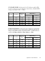
1
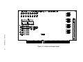
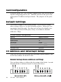
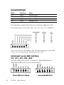
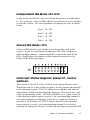
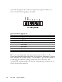
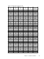
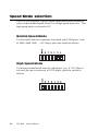
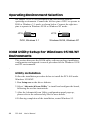
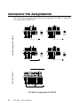
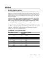
PCL-849
4-Port RS-232
Interface Card
Copyright Notice
This documentation and the software included with this product are
copyrighted 2001 by Advantech Co., Ltd. All rights are reserved.
Advantech Co., Ltd. reserves the right to make improvements to the
products described in this manual at any time without notice.
No part of this manual or software may be reproduced, copied,
translated or transmitted, in any form or by any means without the
prior written permission of Advantech Co., Ltd. Information provided in this manual is intended to be accurate and reliable. However,
Advantech Co., Ltd. assumes no responsibility for its use, nor for any
infringements of rights of third parties which may result from its use.
Acknowledgments
PC-LabCard is a trademark of Advantech Co., Ltd. IBM, PC and
PC/XT/AT are trademarks of International Business Machines
Corporation. MS-DOS, MASM, QuickBASIC, Microsoft C and MSPASCAL are trademarks of Microsoft Corporation. Intel is a trademark of Intel Corporation. Turbo C and Turbo PASCAL are trademarks of Borland International.
Part No. 2000084900 3rd Edition
Printed in Taiwan May 2001
Contents
Chapter 1: Introduction ....................................................... 5
Description ............................................................................. 6
Features .................................................................................. 7
Specifications ......................................................................... 7
Chapter 2: Hardware Installation ....................................... 11
Initial Inspection ................................................................. 12
Card Installation ................................................................. 13
Card Configuration ............................................................ 14
Default Settings ................................................................... 14
I/O Address and Interrupt Setup....................................... 14
Enhanced Mode .................................................................. 15
Speed Mode selection .......................................................... 20
Chapter 3: Software Installation ........................................ 21
Operating Environment Selection ..................................... 22
ICOM Utility Setup for Windows 95/98/NT
Environments ...................................................................... 22
Chapter 4: Wiring .............................................................. 25
Connector Pin Assignments ............................................... 26
Wiring .................................................................................. 27
Chapter A: PC I/O Address Reference ................................ 29
PC I/O Address Usage ......................................................... 30
Chapter B: Quick Reference ............................................... 31
CHAPTER
Introduction
1
Description
The PCL-849 series are four port serial communication interface
cards. Each port can be configured individually to RS-232 using onboard jumpers.
PCL-849A/849B serial ports are implemented using 16C554 UARTs
which make serial I/O more reliable. For higher performance, 16C654
UARTs can be installed in place of the 16C554 to create the PCL849+. By buffering data into 64-byte packets before putting it on the
bus, UARTs drastically reduce the CPU load. This makes the
PCL-849+ especially suitable for high-speed serial I/O applications
under multitasking environments and for applications involving high
data rates.
PCL-849 series cards support two operating modes: standard mode
and enhanced mode. In standard mode each of the four port addresses
can be set individually. In enhanced mode, all four port addresses can
be set automatically. The PCL-849+ also supports either shared IRQ
or independent IRQ functions. When an on-board interrupt occurs the
interrupt status register (vector address) indicates which port generated it. The shared interrupt can be set to most common (extended) AT
interrupts. This simplifies programming, speeds interrupt processing
and frees interrupts for other devices.
6
PCL-849
User's Manual
Features
v
Four independent RS-232 serial ports
v
Transmission speeds up to 307.2 kbps
v
Independent I/O addresses and independent/shared IRQ settings for
each of 4 serial ports
v
Wide IRQ selection: 3, 4, 5, 6, 7, 9, 10, 11, 12, 15
v
Supports Standard DOS COM1, COM2, COM3, and COM4
v
Supports DOS/Windows 3.1, Windows 95/98, Windows NT (ICOM
Utility)
v
Supports surge protection: 3000 VDC (PCL-849B/849+)
v
LED indicators on each port indicate data flow
v
On-board interrupt status register for greater throughput
v
Complete RS-232 Modem-control signals
Specifications
· Bus interface: ISA
· Number of ports: 4
· I/O address: 0x0200 ~ 0x03F8
· IRQ: 3, 4, 5, 6, 7, 9, 10, 11, 12, 15
· Data bits: 5, 6, 7, 8
· Stop bits: 1, 1.5, 2
· Parity: none, even, odd
Chapter 1 Introduction
7
· UART:
1 × 16C554 (PCL-849A/849B)
1 × 16C654 (PCL-849+)
· Speed: 50 ~ 921.6 kbps (PCL-849A)
50 ~ 307.2 kbps (PCL-849B/849+)
· Connectors: 30-cm male DB-37 to 4 × DB25 male (DTE)
· Data signals: TxD, RxD, RTS, CTS, DTR, DSR, DCD, RI, GND
· Surge protection: 3000 VDC (PCL-849B/849+)
· Power requirement: 250 mA typical 500 mA max. (+5 V),
70 mA typical. 120 mA max.(±12 V),
· Dimensions: 185 mm × 98 mm
· Operating Temperature.: 0 ~ 60° C (32 ~ 140° F) (refer to IEC-681.2.3 item)
· Storage Temperature: -25 ~ 80° C (-13 ~ 176° F)
· MTBF: over 135,000 hrs at 25° C, ground-fix environment
· For technical support and service please visit our support website at:
http://support.advantech.com
and visit the "Industrial Automation Support" and "FAQ" sections.
8
PCL-849
User's Manual
Chapter 1 Introduction
Figure 1-1: Switch and jumper layout
9
10
PCL-849
User's Manual
CHAPTER
Hardware
Installation
2
Initial Inspection
Depending on the option you ordered, in addition to this manual, you
should find the following items inside the shipping container:
• PCL-849(A/B/+) 4-port RS-232 Card
• One 30-cm male DB-37 to four male DB-25 cable
• One diskette with ICOM utility software
We have carefully inspected the PCL-849 mechanically and electrically before shipping. It should be free of marks and scratches and in
perfect working order on receipt.
As you unpack the PCL-849, check it for signs of shipping damage
(damaged box, scratches, dents, etc.). If it is damaged or it fails to
meet specifications, notify our service department or your local sales
representative immediately. Also notify the carrier. Retain the
shipping carton and packing material for inspection by the carrier.
After inspection we will make arrangements to repair or replace the
unit.
Remove the PCL-849 from its protective packaging by grasping the
rear metal panel. Keep the anti-vibration packing. Whenever you
remove the card from the PC, store it in this package for protection.
Warning! Discharge your body’s static electric charge by
touching the back of the grounded chassis of the
system unit (metal) before handling the board. You
should avoid contact with materials that hold a static
charge such as plastic, vinyl and styrofoam. Handle
the board only by its edges to avoid static damage to
its integrated circuits. Avoid touching the exposed
circuit connectors.
12
PCL-849
User's Manual
Card Installation
Warning! Turn off your PC’s power supply whenever you install
or remove the PCL-849 or its cables. Static electricity
can easily damage computer equipment. Ground
yourself by touching the chassis of the computer
(metal) before you touch any boards.
1. Turn off the computer. Turn the power off to any peripheral
devices (such as printers and monitors).
2. Disconnect the power cord and any other cables from the back of
the computer. Turn the PC if necessary to gain access to the
cables.
3. Remove the PC’s cover (refer to your user’s guide if necessary).
4. Locate the expansion slots or passive backplane (at the rear of the
PC) and choose any unused slot.
5. Remove the screw that secures the expansion slot cover to the PC
(save the screw to secure the interface card retaining bracket).
Remove the anti-vibration card clamp if supplied.
6. Carefully grasp the upper edge of the PCL-849 card. Align the
hole in the retaining bracket with the hole on top of the expansion
slot. Align the gold striped edge connector with the expansion slot
socket. Press the board firmly into the socket.
7. Replace the screw in the expansion slot retaining bracket. Replace
anti-vibration card holder.
8. Replace the PC’s cover. Connect the cables you removed in step 2.
9. Attach the DB-37 cable to the connector on the bracket. Turn the
computer power on.
The board is now installed in the computer. See Chapter 3 for information on cabling.
Chapter 2 Hardware Installation
13
Card Configuration
Each port on the PCL-849 card has a jumper and a DIP switch which
require configuring prior to use. The DIP switch sets the port to the
appropriate I/O address and speed mode. The jumpers set the port's
IRQ.
Default Settings
The board is shipped with default settings. If you need to change
these settings, however, see the following sections. Otherwise, you
can simply install the card. Note that you will need to disable your
CPU card's on-board COM ports, if any, or set them to alternate
addresses / IRQs.
PCL-849 Default Configuration
Setting
JPI
Default function
IRQ 12
Speed mode
1x
IRQ mode
Share
Base address
Address 300H
Vector address
Interrupt 280H
Address mode
Enhance
I/O Address and Interrupt Setup
Next, you will need to select an IRQ (interrupt request) number, and
an I/O base address for the PCL-849.
Model Setup (base address setting)
The card base address is affected by the setting of the Mode 1 switch.
Standard mode or enhanced mode is selected as shown.
14
PCL-849
User's Manual
Standard Mode
In this mode, each of the four ports is assigned an address, as shown
below.
Port 1
Ch1
base address
3F8
Port 2
Ch2
base address
2F8
Port 3
Ch3
base address
3E8
Port 4
Ch4
base address
2E8
Enhanced Mode
In this mode, the address for each of the four ports is assigned
according to the card base address, which is set using switch S2.
Select an address which is not already in use by another card in the
system. If you are installing more than one PCL-849 card in your
system, set the cards to different base addresses. DIP switches control
each card's base address, as shown below.
Port base address (S2)
Base Address
A3
A4
A5
A6
A7
A8
200-21F
l
l
l
l
l
l
208-227
¡
l
l
l
l
l
¡
l
¡
¡
¡
l
l
l
l
l
l
¡
l
l
¡
¡
¡
¡
··········
2E8-307
··········
*300-31F
··········
3E0-3FF
l: on
¡ : off
*= default
Chapter 2 Hardware Installation
15
Default Settings
Mode
Enhanced
Mode
Port 1
IRQ12
Address 300H
Port 2
IRQ12
Address 308H
Port 3
IRQ12
Address 310H
Port 4
IRQ12
Address 318H
The following example shows how to set the base address to 2F8.
The switch sum is set to 2F8: 200 + 80 + 40 + 20 + 10 + 8 (HEX).
Note: On the PCL-849 address line A9 does not appear on the DIP
switch, as it is permanently hardwired to hex 200.
Interrupt Level (IRQ) Setting
(S1, JP1, JP2, JP3, JP4)
The card's IRQ mode can be set using S1. Shared IRQ mode or
independent IRQ mode is set as shown below.
16
PCL-849
User's Manual
Independent IRQ Mode (JP1-JP4)
In this mode, the IRQ level for each of the four ports is set individually. For each port, select an IRQ which is not already in use by another
card in the system. The correspondence of jumpers to ports is shown
below.
Port 1 à JP1
Port 2 à JP2
Port 3 à JP3
Port 4 à JP4
Shared IRQ Mode (JP1)
Select an IRQ which is not already in use by another card in the
system. If you are installing more than one PCL-849, set them to
different IRQ numbers. Jumper Bank JP1 controls the shared card
IRQ. Simply place the jumper on the required interrupt level as
shown in the following figure.
Interrupt Status Register Setup (S1, Vector
address)
This feature on the PCL-849 is utilized in the enhanced mode only.
When data arrives at one of the four ports, it will generate an interrupt
in the interrupt register. The PC software can read this, and identify
immediately which port generated the interrupt. This saves time, and
makes programming easier. In DOS or Windows 3.1, when a data bit
of the interrupt status register is set to 0, the corresponding channel is
selected to generate an interrupt. If the bit is 1, then no interrupt is
generated. In Windows 95/98/NT, when a data bit of the interrupt
status register is set to 1, the corresponding channel is selected to
generate an interrupt. If the bit is 0, then no interrupt is generated. DIP
Chapter 2 Hardware Installation
17
switch S1 designates the card's interrupt status register address, as
shown in the following figure and table.
Interrupt Status Register S1
Bit
Function
0
Port 1
1
Port 2
2
Port 3
3
Port 4
4
Not Used
5
Not Used
6
Not Used
7
Not Used
The user may change the interrupt status register address via S1.
Please note that the address decoder will occupy a continuous, 16-byte
area related to the switch setting. For example, if you set the switch to
210H, then the address 210H to 21FH will all be decoded. The
various DIP switch settings (S1) for the interrupt status register are as
shown in the table opposite.
18
PCL-849
User's Manual
Table 2-1: DIP switch settings for S1
A4
A5
A6
A7
A8
Interrupt
Register
ON
ON
ON
ON
ON
200H
OFF
ON
ON
ON
ON
210H
ON
OFF
ON
ON
ON
220H
OFF
OFF
ON
ON
ON
230H
ON
ON
OFF
ON
ON
240H
OFF
ON
OFF
ON
ON
250H
ON
OFF
OFF
ON
ON
260H
OFF
OFF
OFF
ON
ON
270H
280H
ON
ON
ON
OFF
ON
OFF
ON
ON
OFF
ON
290H
ON
OFF
ON
OFF
ON
2A0H
OFF
OFF
ON
OFF
ON
2B0H
ON
ON
OFF
OFF
ON
2C0H
OFF
ON
OFF
OFF
ON
2D0H
ON
OFF
OFF
OFF
ON
2E0H
OFF
OFF
OFF
OFF
ON
2F0H
ON
ON
ON
ON
OFF
300H
OFF
ON
ON
ON
OFF
310H
ON
OFF
ON
ON
OFF
320H
OFF
OFF
ON
ON
OFF
330H
ON
ON
OFF
ON
OFF
340H
OFF
ON
OFF
ON
OFF
350H
ON
OFF
OFF
ON
OFF
360H
OFF
OFF
OFF
ON
OFF
370H
ON
ON
ON
OFF
OFF
380H
OFF
ON
ON
OFF
OFF
390H
3A0H
ON
OFF
ON
OFF
OFF
OFF
OFF
ON
OFF
OFF
3B0H
ON
ON
OFF
OFF
OFF
3C0H
OFF
ON
OFF
OFF
OFF
3D0H
ON
OFF
OFF
OFF
OFF
3E0H
OFF
OFF
OFF
OFF
OFF
3F0H
Chapter 2 Hardware Installation
19
Speed Mode selection
The PCL-849 employs a unique speed option that allows the user to
choose either normal speed mode (1x) or high speed mode (8x). This
high speed mode is selected at S2.
Normal Speed Mode
To select the baud rate commonly associated with COM ports , such
as 2400, 4800, 9600. . .115.2 kbps, place the switch as follows.
High Speed Mode
To increase normal mode rates by eight times, (e.g. if 115.2 kbps is
selected, the rate is increased to 921.6 kbps), place the switch as
follows.
20
PCL-849
User's Manual
CHAPTER
Software
Installation
3
Operating Environment Selection
Set jumper 15 (JP15) to correspond with your desired software
operating environment. Connect the left two pins of JP15 to operate in
DOS or Windows 3.1 mode, as shown below. Connect the right two
pins to operate in Windows 95/98 or Windows NT mode .
1
JP15
JP15
DOS, Windows 3.1
1
Windows 95/98, Windows NT
ICOM Utility Setup for Windows 95/98/NT
Environments
This section discusses the ICOM utility software package installation,
configuration and upgrade/ removal procedure for the Windows 95/98
and NT environments.
.
Utility Installation
Follow the installation procedure below to install the PCL-849 under
Windows 95/98/NT:
1. Run Setup.exe on the driver diskette.
2.Select “Advantech Icom Utility” to install and configure the board,
following the on-line instructions.
3.After the Advantech Icom Utility configuration panel pops up,
please refer to the software help file for more details.
4.Following completion of the installation, restart Windows 95.
22
PCL-849
User's Manual
Following completion of installation, please restart your system as
prompted.
Once the board and driver have been installed and the system
restarts successfully, users can execute any ready-made applications, such as HyperTerminal to transmit/receive data, or Remote
Access Service to provide dial-up networking capability.
Configuration:
Enter the configuration program to install the device driver, or click
the Taskbar [Start] button, then select the [Programs] menu, then the
[Advantech Icom Utility] menu and then [Icom].
When the configuration panel pops up,
click the [Add Board] button to add a board.
Click the [Delete] button to remove a board.
Board Type: PCL-849
Base COM: Specifies the COM number of the first port. Subsequent
ports are mapped to subsequent COM numbers. For instance, if the
first port is mapped to COM10, then the second port is mapped to
COM11 sequentially.
Base Address (200H~3F8H): Specifies the base address of the first
port. Subsequent base addresses are mapped to subsequent COM
numbers. For instance, if the first port is mapped to 300H, then the
second port is mapped to 308H sequentially.
PCL-849 series cards can be installed together in a single system as
long as the system memory resources are sufficient and available in a
system. Different boards should be assigned different IRQs.
Click the [Share IRQ Enable] button to set the share IRQ function.
Chapter 3 Software Installation
23
Share IRQ: 3, 4, 5, 6, 7, 9, 10, 11, 12, 15
Vector Address: 200H ~ 3F0H
After you finish the installation, you can click [Exit] and restart your
system. Unless the system is restarted, the latest configuration will not
take effect.
24
PCL-849
User's Manual
CHAPTER
Wiring
4
Chapter 4 Wiring
25
Connector Pin Assignments
PCL-849: DB-37
Four Port Connectors: DB-25
The following diagrams show the pin assignments for DB-37 and DB25 connectors for RS-232.
PCL-849 Pin assignments for RS-232
26
PCL-849
User's Manual
Wiring
RS-232 signal wiring
Since the RS-232 interface is not strictly defined, many devices have
their own connection methods which may ignore some signal lines or
define reserved lines for other functions. It is best to refer to the user’s
manual for your device for installation instructions. You may find the
following helpful.
In general, DTE (Data Terminal Equipment) refers to the device that
is leading the communication. Examples include PC’s, terminals and
some printers. DCE refers to the device being communicated with or
controlled. Examples include modems, DSU’s (digital service units),
printers and lab/factory equipment.
In some situations you may be able to get by with just three lines: data
on TXD, a signal ground and a handshaking line. Examples are printer
or plotter connections, troubleshooting and situations where you
require only one-wire communication.
Terminal or PC (DTE) connections
DB-25 Male: PCL-849
DB-25 Male or Female:
Terminal
Pin
2
Signal
TxD
Pin
3
Signal
RxD
3
RxD
2
TxD
4
RTS
5
CTS
5
CTS
4
RTS
6
DSR
20
DTR
7
GND
7
GND
20
DTR
6
DSR
8
DCD
8
DCD
Chapter 4 Wiring
27
Modem connections
DB-25 Male: PCL-849
Modem (DCE)
Pin
2
Signal
TxD
Pin
2
Signal
RxD
3
RxD
3
TxD
4
RTS
4
CTS
5
CTS
5
RTS
6
DSR
6
DTR
7
GND
7
GND
20
DTR
20
DSR
8
DCD
8
DCD
For DTE to DCE connections, use straight through cable (i.e., you
don't have to reverse lines 2 and 3, lines 4 and 5, and lines 6 and 20
since, in general, the DCE RS-232 interfaces are reversed themselves).
Terminal without handshake
28
DB-25 Male: PCL-849
Terminal, PC (DTE)
Pin
2
Pin
3
Signal
RxD
2
TxD
7
GND
Signal
TxD
3
RxD
4
5
RTS
CTS
7
GND
6
20
8
DSR —
DTR —
DCD —
PCL-849
—
—
User's Manual
APPENDIX
PC I/O Address
Reference
A
Appendix A PC I/O Address Assignments
29
PC I/O Address Usage
The following table indicates the PC I/O address usage assignments.
To prevent the PCL-849 card settings from conflicting with other
device or I/O card settings, we recommend you refer to this table.
30
I/O Address
Device
000 - 00F
DMA (8237A)
020 - 021
8259A IRQ Controller
040 - 043
8253/8254 Timer/Counter
060 - 063
PPI 8255A
070 - 071
Real-Time Clock
080 - 08F
DMA Page Register
0A0 - 0BF
8259A Interrupt Chip
0C0 - 0DF
Second DMA Controller 8237A
0F0 - 0FF
Math Coprocessor
1F0 - 1F8
AT Fixed Disk
200 - 20F
Game I/O
278 - 27F
Parallel Printer Adaptor #2
2F8 - 2FF
Serial Adaptor ( COM 2 )
320 - 32F
XT Fixed Disk
378 - 37F
Parallel Printer Adaptor #1
380 - 38F
SDLC Binary Communication Adaptor
3A0 - 3AF
Master Binary Communication Adaptor
3B0 - 3BF
Monochrome/Parallel Adaptor
3D0 - 3DF
Color Graphics Adaptor
3F0 - 3F7
Diskette Controller
3F8 - 3FF
Serial Adaptor ( COM 1 )
PCL-849
User's Manual
APPENDIX
Quick
Reference
B
Appendix B Quick Reference
31
Ø Jumper Setting
·
IRQ Mode
DIP 1 (MODE 0) of S1 is used to set the IRQ mode of this card.
DIP1 : ON (Upper) position
è Shared IRQ mode
DIP1 : OFF (Lower) position
è Independent IRQ mode
·
STANDARD/ ENHANCED Mode
DIP 2 (MODE 1) of S1 is used to set the standard/enhanced mode of
this card.
DIP1 : ON (Upper) position
è STANDARD mode
DIP1 : OFF (Lower) position
è ENHANCED mode
·
SPEED Mode
DIP 1 (SPEED) of S2 is used to determine the speed mode of this
card.
Ø Operating System Mode
Connect the left two pins of JP15 to use DOS, Windows 3.1
Connect the right two pins of JP15 to use Windows 95/98/ NT
DIP1 : ON (Upper) position è High Speed Mode or ´ 8 Mode
(Frequency of Oscillator Crystal = 14.7456 MHz)
DIP1 : OFF (Lower) position è Normal Speed Mode
(Frequency of Oscillator Crystal = 1.8432 MHz)
32
PCL-849
User's Manual
STANDARD MODE: In this mode, the I/O addresses and the IRQ
levels for each port are set to default as shown below, (Disable BIOS
setting of on-board COM1 ~ COM4)
Port No.
I/O Address
COM Port
No.
Port 1
3F8h
Port 2
IRQ Level (*)
Independent IRQ
Shared IRQ
COM1
JP1
JP1
2F8h
COM2
JP2
JP1
Port 3
3E8h
COM3
JP3
JP1
Port 4
2E8h
COM4
JP4
JP1
ENHANCED MODE: In this mode, the I/O addresses and the IRQ
levels for each port are set as shown below, (Make sure that the I/O
address on the BIOS setting of on-board COM1 ~ COM4 will never
conflict with [Base Address] ~ [Base Address + 1Fh])
Port No.
Port 1
Port 2
Port 3
Port 4
I/O Address
Base Address
+ 00h
Base Address
+ 08h
Base Address
+ 10h
Base Address
+ 18h
COM Port
No.
IRQ Level (*)
Independent IRQ
Shared IRQ
COM1
JP1
JP1
COM2
JP2
JP1
COM3
JP3
JP1
COM4
JP4
JP1
Appendix B Quick Reference
33
34
PCL-849
User's Manual