1
LBI-38557
2.
3.
4.
LBI-38557
Check power on the lower channel. Adjust C124 in the
direction that increases power output to a level half way
between the initial lower and upper channel levels.
Recheck the upper channel power. If the upper channel
power is reduced, reset to the previous level by adjusting C126.
Repeat this procedure until the power out on both
channels is equal (±.1W).
•
•
For frequency spreads ≤ 10 MHz - power out ≥
power minimum
For frequency spreads > 10 MHz - power out ≥
power minimum - 1dB
Supply current levels should not exceed 1100 mZ
(10V) or 800 mA (7.5V) with wide band tuning.
TX Modulation Set
With the transmitter keyed, apply a 1 kHz tone at 100 mV
RMS to the MIC input. Adjust R230, located on the Synthesizer Board, until the following peak deviation is measured on
the output modulation analyzer:
With Channel Guard - 4.5 kHz (±100 Hz)
Without Channel Guard - 3.75 kHz (±100 Hz)
Second LO Frequency Set
Remove all modulation from the input signal and increase
the level to 0 dBm. Monitor the frequency at J501 and adjust
L505 in the crystal oscillator circuit for 455 kHz ±100 Hz.
Modulate the RF input signal with a 1 kHz tone at 3 kHz
peak deviation. Load the speaker output at the accessory connector with 8 ohms to ground. Monitor the speaker output from
the accessory connector while tuning L506 in the quardrature
detector for a maximum audio level.
L.O. Notch Tuning
When it necessary to limit the L.O. leakage out the antenna
port to a level less than -60 dBm, (Canadian D.O.C. RSS 119,
121 require -53 dBm for portables with batteries, otherwise -57
dBm) the L.O. notch filter may be tuned to the receiver L.O.
frequency to meet this requirement. Observe the L.O. signal
level at the antenna port on a spectrum analyzer capable of
reading -70 dBm. Select the channel with the lower operating
receive frequency and tune the notch filter adjustable capacitor
(C136) for a minimum level. Check the level on the higher
receive frequency. If greater than -60 dBm, turn the capacitor
(C136) in the direction that lowers the level to the point that
-60 dBm is reached and stop. Recheck the lower receive
frequency.
TROUBLESHOOTING
IF Alignment
This section provides a guide to troubleshooting the MPIII VHF radio. The following procedures will assist in determing if the problem is in the RF circuits (Transmitter,
Receiver or Synthesizer) or the Control circuits. The test set-up
should be the same as that used in the Alignment section of this
manual.
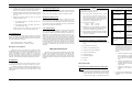
Tabel 2 - General Troubleshooting Guide
Throughout the service procedures, the following
information should be observed:
•
Quadrature Detector Set
RECEIVE ALIGNMENT
Change to a receiver test setup, with a frequency modulated RF signal generator connected to the antenna jack J3. Set
the input RF signal to the highest programmed receive frequency and modulate it with a 1 kHz tone at 5 kHz peak
deviation. Use a signal level high enough to measure the level
of the 455 kHz 2nd IF signal at test point J501 with an RF AC
voltmeter. Proceed with the following alignment procedure.
NOTE
•
•
•
The bench power should be set for 7.5 Vdc
(±0.1 Vdc) for a 2 watt radio, or 10.0 Vdc (±0.1
Vdc) for a 4 watt radio. If a battery pack is
used, it should be fully charged. Typical battery
pack voltage should be within ±20% of set
voltage over its full discharge cycle.
Logic Levels should be:
Logic 1 = high ≤ 4.5 Vdc
Logic 0 = low ≥ 0.5 Vdc
The personality information stored in the radio
should be backed up on the PC computer before
any service procedure.
•
•
•
•
•
•
•
•
•
•
•
Dead Battery Pack
Fuse blown
Control circuit problem
At power-up radio
beeps continuously
•
•
•
Weak battery pack
Unit is not programmed
Synthesizer is not locked
Receiver inoperative
or weak
•
•
•
•
Squelch level set too high
Channel Guard enabled
Defective antenna
T/R Board problem
Transmitter inopeative or low range
•
•
•
•
Power levels set too low
Weak battery
Defective antenna
T/R Board problem
Tx and Rx inoperative on one or both
channels
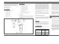
RX and TX block diagrams with RF gains and
levels
•
•
S
E
R
V
I
C
E
S
E
C
T
I
O
N
Programming incorrect
Synthesizer problem:
VCO, prescaler, or
lock detect
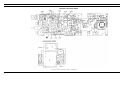
Interconnection diagram
troubleshooting a personal radio. Current consumption offers an excellent clue in the case of a dead or
weak transmitter. See Table 3 in the Battery Information section on typical current consumption for different operating conditions. Check supplies as
follows:
Outline diagrams
a.
Check for battery B+ voltage at J12-01, or inside
fuse F1/switch S1. It should be present at the
driver Q104 and final amplifier Q105, and measure 7.5 Vdc for 2-watt radio, 10 Vdc for 4-watt
radio.
b.
Check for presence of B+ SW on buffer amplifier Q106 and predriver Q103. It should switch
ON under control of the PTT switch through B+
switch Q805.
c.
Check 5.4 V from 5.4 V regulator, which is
required for and available on the Synthesizer
board.
Synthesizer block diagram
Control Circuits block diagram
Audio Processing block diagram
Schematic diagrams
Parts lists
IC data
Adjust the RF signal level for linear operation at J501.
Tune L502 and L504 for a maximum IF signal level at J501.
TRANSMITTER
An alternate method for making the IF alignment is as
follows. Tune L502 and L504 for minimum audio distortion
while monitoring the speaker output. Use either 5 kHz or 3 kHz
of deviation.
Transmit Power Output Problem, Inoperative
or Low
1.
POSSIBLE CAUSES
Completely inoperative (no audio)
Modules are not field repairable. Schematics
and Outline drawings for the modules are presented for troubleshooting reference only.
Documentation To Help In Troubleshooting
•
SYMPTOM
Power sources and regulated power supplies should
be checked before troubleshooting any transmitter
problem. The radio’s power source, whether a battery
or bench power supply, is especially important in
2.
An early step in troubleshooting for the cause of low
RF output power is to check that the programming is
correct.
5