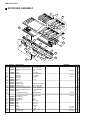
1
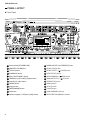
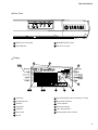
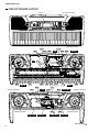
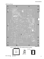
SERVICE MANUAL
PSR-280
PSR-282
This document is printed on chlorine free (ECF) paper with soy ink.
PK
CONTENTS
SPECIFICATIONS ···································································· 3
PANEL LAYOUT······································································· 4
CIRCUIT BOARD LAYOUT ······················································ 6
BLOCK DIAGRAM ···································································· 8
DISASSEMBLY PROCEDURE················································· 9
LSI PIN DESCRIPTION ·························································· 12
IC BLOCK DIAGRAM ····························································· 14
CIRCUIT BOARDS ································································· 15
TEST PROGRAM ··································································· 24
DATA INITIALIZATION ··························································· 26
MIDI IMPLEMENTATION CHART ·········································· 27
PARTS LIST
OVERALL CIRCUIT DIAGRAM
001641
HAMAMATSU, JAPAN
1.43K-257
Printed in Japan '00.06
PSR-280/PSR-282
IMPORTANT NOTICE
This manual has been provided for the use of authorized Yamaha Retailers and their service personnel. It has been assumed that
basic service procedures inherent to the industry, and more specifically Yamaha Products, are already known and understood by
the users, and have therefore not been restated.
WARNING:
Failure to follow appropriate service and safety procedures when servicing this product may result in personal
injury, destruction of expensive components and failure of the product to perform as specified. For these
reasons, we advise all Yamaha product owners that all service required should be performed by an authorized
Yamaha Retailer or the appointed service representative.
IMPORTANT:
This presentation or sale of this manual to any individual or firm does not constitute authorization, certification,
recognition of any applicable technical capabilities, or establish a principal-agent relationship of any form.
The data provided is belived to be accurate and applicable to the unit(s) indicated on the cover. The research engineering, and
service departments of Yamaha are continually striving to improve Yamaha products. Modifications are, therefore, inevitable and
changes in specification are subject to change without notice or obligation to retrofit. Should any discrepancy appear to exist,
please contact the distributor's Service Division.
WARNING:
Static discharges can destroy expensive components. Discharge any static electricity your body may have
accumulated by grounding yourself to the ground bus in the unit (heavy gauge black wires connect to this bus).
IMPORTANT:
Turn the unit OFF during disassembly and parts replacement. Recheck all work before you apply power to the
unit.
WARNING: CHEMICAL CONTENT NOTICE!
The solder used in the production of this product contains LEAD. In addition, other electrical/electronic and/or plastic (where
applicable) components may also contain traces of chemicals found by the California Health and Welfare Agency (and possibly
other entities) to cause cancer and/or birth defects or other reproductive harm.
DO NOT PLACE SOLDER, ELECTRICAL/ELECTRONIC OR PLASTIC COMPONENTS IN YOUR MOUTH FOR ANY REASON
WHAT SO EVER!
Avoid prolonged, unprotected contact between solder and your skin! When soldering, do not inhale solder fumes or expose eyes
to solder/flux vapor!
If you come in contact with solder or components located inside the enclosure of this product, wash your hands before handling
food.
WARNING
Components having special characteristics are marked
originally installed.
2
and must be replaced with parts having specification equal to those
PSR-280/PSR-282
SPECIFICATIONS
Keyboards
• 61 standard-size keys (C1 - C6), with Touch Response and
Dynamic Filter.
MIDI
• Clock
• Bulk Send/Receive
• Initial Send
Display
• Large multi-function LCD display (backlit)
Auxiliary jacks
• PHONES/OUTPUT, DC IN 10-12 V, MIDI IN/OUT, SUSTAIN
Setup
• STANDBY/ON
• MASTER VOLUME: MIN - MAX
Panel Controls
• OVERALL (L, R), SONG, VOICE, STYLE, PORTABLE
GRAND, DJ, METRONOME, [0]-[9], [+](YES), [-](NO),
DEMO, TOUCH, HARMONY, Dict., L, R, TEMPO/TAP
Amplifier
• 3.0 W + 3.0 W
Speakers
• 12 cm x 2 + 3 cm x 2
Power Consumption
• 15 W (when using PA-3B power adaptor)
Voice
• 118 panel voices + 10 Drum Kits + 128 GM Voices
• Polyphony: 32
• Voice Set
Auto Accompaniment
• 100 styles
• Accompaniment Control: ACMP ON/OFF, SYNC STOP,
SYNC START, START/STOP,
INTRO/ENDING, MAIN A/B(AUTO
FILL)
• Fingering : Multi fingering
• Accompaniment Volume
Yamaha Educational Suite
Power Supply
• Adaptor: Yamaha PA-3B AC power adaptor
• Batteries: Six “D” size, SUM-1, R-20 or equivalent batteries
Dimensions (W x D x H)
• 933 x 370 x 129 mm (36-3/4" x 14-5/8" x 5-1/6")
Weight
• 5.5 kg (12 lbs., 2 oz.)
Supplied Accessories
• Music Stand
• Owner’s Manual
• Song Book
• Dictionary
• Lesson 1-4
One Touch Setting
• Voice (for each style or song)
Overall controls
•
•
•
•
•
•
•
•
•
•
•
Transpose
Tuning
Accompaniment Volume
Song Volume
Metronome Volume
MIDI
Reverb
DSP
Harmony
Grade
Talking
Optional Accessories
•
•
•
•
Headphones:
AC power adaptor:
Footswitch:
Keyboard stand:
HPE-150
PA-3B
FC4, FC5
L-2L, L-2C
Effects
• Reverb:
8 types
• DSP:
37 types
• Harmony: 26 types
Song
• 100 Songs + 5 User Songs
• Song Clear, Track Clear
Recording
• Song
User Song:
5 Songs
Real Time Recording
Recording Tracks: 1, 2, 3, 4, 5, CHORD
3
PSR-280/PSR-282
PANEL LAYOUT
Front Panel
3
4
7
7
12
8
1
10
5
2
6
9
20
21
11
22
19
13 14 15
4
16
17
23
18
24
1 Power switch ([STANDBY/ON])
13 [ACMP ON/OFF] / [A-B REPEAT] button
2 [MASTER VOLUME] dial
14 [SYNC STOP] button
3 [TOUCH] button
15 [SYNC START] / [
4 [HARMONY] button
16 [START/STOP] button
5 [Dict.] (DICTIONARY) button
17 [INTRO/ENDING] / [
6 LESSON [L] (Left) and [R] (Right) buttons
18 [MAIN/AUTO FILL] / [
7 Overall (left, right) buttons
19 [TEMPO/TAP] button
8 [DEMO] button
20 [SONG] button
9 [Piano] button
21 [STYLE] button
10 [METRONOME] button
22 [VOICE] button
11 [DJ] button
23 [SONG MEMORY] buttons
12 Numeric keypad, [+/YES] and [-/NO] buttons
24 REGISTRATION MEMORY buttons
PAUSE] button
REW] button
FF] button
PSR-280/PSR-282
Rear Panel
25
26
27
28
25 MIDI IN, OUT terminals
27 PHONES/OUTPUT jack
26 SUSTAIN jack
28 DC IN 10-12V jack
Display
30
36
38 39
29
33
40 41
31 32
37
35
34
29 Indicators
36 Song/Voice/Style name and number, Tempo
30 Overall indicator
37 Song track indicators
31 Notation
38 Touch indicator
32
Keyboard
39 Harmony indicator
33
Measure
40 Sync Stop indicator
34 Beat marks
41 Accompaniment On indicator
35 Chord
5
PSR-280/PSR-282
CIRCUIT BOARD LAYOUT
LCD unit
Upper case assembly
Keyboard assembly
WH500
CN101
WH200
380
380
CN820
WH300
WH020
Speaker R (Tweeter)
MKS3
WH400
L70
MK-L
WH400
L70
LCD
WH010
WH500
PN(PW)
WH040
CN704
CN801
CN1
CN703
CN701
Speaker L (Tweeter)
CN911
MK-H
CN912
CN810
CN501
WH300
WH050
CN801
CN601 CN702
DM
WH060
CN601
CN701
CN102
AM
WH100
CN910
CN911
WH040
CN101 CN501
390
380
CN705
CN706
WH030
Speaker R (Woofer)
PN(PNR) PN(PNC)
PN(PNL)
WH050
Speaker L (Woofer)
PN(VR)
2NC-V524070
6
3
PSR-280/PSR-282
Location
Part No.
Connector Assembly
Destination
Remarks
WH010
(V539010)
DM-PN-R
PN(PNR)-CN701
DM-CN702
14P
WH020
(V539100)
PN-R-PN-L
PN(PNR)-CN703
PN(PNL)-CN704
9P
WH030
(V539110)
PN-L-PN-C
PN(PNL)-CN705
PN(PNC)-CN706
4P
WH040
(V539030)
DM-VR
PN(VR)-CN501
DM-CN501
4P
WH050
(V539060)
AM-VR
PN(VR)-CN801
AM-CN801
4P
WH060
(V539040)
AM-PSW
PN(PW)-CN911
AM-CN911
4P
WH100
(V538990)
DM-AM1
AM-CN101
DM-CN101
5P
WH200
(V539000)
DM-AM2
AM-CN601
DM-CN601
6P
WH300
(V539140)
AM-SP-R
AM-CN810
SPEAKER R
2P
SPEAKER R
SPEAKER L
WH400
(V560490)
AM-SP-L
AM-CN820
2P
SPEAKER L
WH500
(V538980)
DM-LCD
LCD-CN1
DM-CN701
12P
L70
(V539120)
AM-LCD
LCD UNIT
AM-CN912
2P
380
(V539130)
AM-POWER
POWER SUPPLY
AM-CN910
2P
390
(V616910)
DM-MKS
KEYBOARD ASSEMBLY
DM-CN102
6P
* Connector assembly listed above are not available as service parts.
7
8
CL001
CLOCK
8.4672MHz
IC103
9
1
CN102
CN1
IC502
IC501
CN801
PN(VR)
MASTER
VOLUME
CN501
LPF
DAC
5~7
156
CN501
ADIN
TXD0
CN801
AM
EQ
IC601
6
2
IC810
IC810
IC301
IC302
MIDI I/F
1M SRAM
1M SRAM
C-BUS D0~15, A0~20
4
1
WAVE
IC201
PROGRAM
IC202
7
1
+5D
+3.3D
ROM1
32M ROM
IC701
7
2
3
CN1
LCD
DRIVER
ROM2
C1~C16,
S1~S40
8M ROM
PAD0~5, PDT0~7, 11, 12
+5V
S-BUS D0~15, A0~20
153
20
LD701
LCD
BUCKLIGHT
LCD
DISPLAY
LCD
CN701
RXD0
DO0, WCLK, QCLK
158, 163, 164
IC101
SWX00
IC1
CPU
TXD1, LSIIC, RXD1, SCLKI
CL1
8MHz
MKS3
Keyboard SW MATRIX
RESET
4.2V
DM
MK
IC820
7
5
+ 6
IC800
POWER
AMP
3W x 2
IC820
3
+
1
2
IC102
+ 14
12
17
+ 15
+3.3V REG
CN601
CN101
1
2
CN601
3
CN101
2
+5V
CN702
CN701
SW MATRIX
PN(PNL, PNC, PNR)
IC930
+5V REG
IC920
+5V REG
IC940
+5V REG
2
1
1
CN911
CN911
SW60
CN810
CN820
JK620
STANDBY/ON
PN(PW)
1
2
1
2
Tweeter R
28CA1-8816895
SP-R 4
PHONES/
OUTPUT
SP-L 4
Tweeter L
SUSTAIN
JK640
MIDI IN
MIDI OUT
JK630
DC IN
10-12V
JK900
BATTERIES
1.5V x 6
CN910
PSR-280/PSR-282
BLOCK DIAGRAM
PSR-280/PSR-282
DISASSEMBLY PROCEDURE
1.
Lower Case Assembly
1-1
Remove the battery cover assembly. (Fig. 1)
1-2
Remove the fifteen (15) screws marked [260A] and two
(2) screws marked [270A]. The lower case assembly can
then be removed. (Fig. 1)
[260A]
[270A]
[270A]
[260A]
[260A]
[260A]
Battery cover assembly
[260A]: Bind Head Tapping Screw-P 3.0 x 12 MFZN2Y (EP600300)
[260A]
Lower case assembly
[270A]: Bind Head Tapping Screw-P 3.0 x 25 MFZN2Y (VK228100)
(Fig. 1)
2.
Circuit Board and Units on the Panel Asseembly
After removing the lower case assembly. (See Procedure 1.)
Remove the following screws, each circuit board and can be removed. (Fig. 2)
Circuit Board and Unit
DM
AM
PN(PW)
MKS3
Keyboard Assembly
Speaker R
(Tweeter)
Ref. No.
[260B]
[240]
[250A]
[250B]
[A]
[30]
[270B]
DM
Lower shield box
[250C]
[280]
Screw
Bind Head Tapping Screw-P 3.0 x 12 MFZN2Y
Bind Head Tapping Screw-B 3.0 x 8 MFZN2Y
Bind Head Tapping Screw-P 3.0 x 8 MFZN2Y
Bind Head Tapping Screw-P 3.0 x 8 MFZN2Y
Push Knob
Bind Head Tapping Screw-P 3.0 x 8 MFZN2Y
Bind Head Tapping Screw-P 3.0 x 25 MFZN2Y
AM
[260B]
[260B]
[250A]
(EP600300)
(EP600250)
(EP600280)
(EP600280)
(VQ218800)
(EP600280)
(VK228100)
PN(PW)
[250A]
[250B]
[280]
[250C]
QTY
5
9
7
2
1
2
3
Speaker L
(Tweeter)
[250C]
[250C]
Speaker R
(Woofer)
Speaker L
(Woofer)
[240]
–
+
–
[270B]
+
[270B]
[260B]
Keyboard assembly
[250A]
[270B]
[250C]: Bind Head Tapping Screw-P 3.0 x 8 MFZN2Y (EP600280)
MKS3
[250A]
[A]
[30]
[280]: Bind Head Tapping Screw-P 4.0 x 8 MFZN2BL (VB931600)
(Fig. 2)
9
PSR-280/PSR-282
3.
Speakers
4.
PN(VR), PN(PNL) Circuit Boards
3-1
3-2
Remove the lower case assembly. (See Procedure 1.)
Woofer:
Remove the four (4) screws marked [280]. The right and
left speakers (woofer) can then be removed. (Fig. 2)
Tweeter:
Remove the two (2) screws marked [250C]. The right and
left speakers (tweeter) can then be removed. (Fig. 2)
4-1
4-2
4-3
Remove the lower case assembly. (See Procedure 1.)
Remove the AM circuit board. (See Procedure 2.)
PN(VR) Circuit Board:
Remove the three (3) screws marked [250D]. The PN(VR)
circuit board can then be removed. (Fig. 3)
PN(PNL) Circuit Board:
Remove the six (6) screws marked [250E]. The PN(PNL)
circuit board can then be removed. (Fig. 3)
3-3
4-4
LCD
[250G]
[250G]
PN(PNR)
PN(VR)
[250H] [250E]
[L50]
[250D]
[250H]
[250H]
[250F] [250F]
[250G]
LCD unit
[250E]
[250H]
[250E]
PN(PNL)
PN(PNC)
[250]: Bind Head Tapping Screw-P 3.0 x 8 MFZN2Y (EP600280)
[L50]: Bind Head Tapping Screw-P 3.0 x 8 MFZN2Y (EP600280)
(Fig. 3)
5.
PN(PNC), PN(PNR), LCD Circuit Boards
6.
Disassembling the keyboard assembly
5-1
5-2
5-3
5-4
Remove the lower case assembly. (See Procedure 1.)
Remove the DM circuit board. (See Procedure 2.)
Remove the AM circuit board. (See Procedure 2.)
PN(PNC) Circuit Board:
Remove the three (3) screws marked [250F]. The PN(PNC)
circuit board can then be removed. (Fig. 3)
PN(PNR) Circuit Board:
Remove the eight (8) screws marked [250G]. The PN(PNR)
circuit board can then be removed. (Fig. 3)
LCD Circuit Board:
Remove the four (4) screws marked [250H]. The LCD unit
can then be removed. (Fig. 3)
Remove the eight (8) screws marked [L50]. The LCD circuit
board can then be removed. (Fig. 3)
When re-install the LCD, place it so that the small protrusion
on the LCD faces the inside on the right. (Fig. 4)
6-1
6-2
Remove the keyboard assembly. (See Procedure 2.)
Remove the two (2) screws marked [30]. The MKS3 circuit
board can then be removed. (Fig. 2)
Remove the MK circuit board while pressing the fifteen
(15) hooks A inward, and then remove the rubber contact.
(Fig. 5)
Remove the twenty-one (21) screws marked [140], then
remove the black keys from the lower notes. Afterwards,
remove the white keys DFA and C' and then remove the
white keys CEGB from the higher notes. At this time, lift
the keys from the front and slide them towards you.The
keys can then be removed from the assembly. (Fig. 6)
5-5
5-6
*
6-3
6-4
• LCD unit
Rubber connector
Conductor side
Rubber connector
(Fig. 4)
10
PSR-280/PSR-282
[140]
Black Keys
Hooks A
MK
White Keys DFA
White Keys
Black Keys
Rubber contact
White Key C'
(Fig. 5)
White Keys CEGB
[140]: Bind Head Tapping Screw-P 3.0 x 16 MFZN2Y (EP600310) or
[140]: Bind Head Tapping Screw-P 3.0 x 16 MFZN2BL (VB205200) or
[140]: Bind Head Tapping Screw-P 3.0 x 16 MFZN2B (VS756700)
(Fig. 6)
7.
Assembling the keyboard assembly
7-1
Install the white keys CEGB from the lower notes, and
then install the DFA keys and C' key. Afterwards install
the black keys from the higher notes, and tighten the
twenty-one (21) screws marked [140]. (Fig. 6)
Install the rubber contacts in the assembly while pressing
the keys as shown in Figure 9. Check that the rubber
contact has been firmly placed into position in the area
indicated by the arrow Figure 10.
7-2
*
When fitting the rubber contacts, raise both ends of the
frame so that do not push the rubber contact up. Install the
MK circuit board in the assembly so that the hooks B hold
it as shown in Figure 11. (Fig. 7, 8, 9)
Rubber contact
Rubber contact
(Fig. 8)
MK
Hooks B
(Fig. 7)
(Fig. 9)
11
PSR-280/PSR-282
LSI PIN DESCRIPTION
HG73C205AFD (XU947C00) SWX00B (Tone Generator)
PIN
NO.
1
2
3
4
5
6
7
8
9
10
11
12
13
14
15
16
17
18
19
20
21
22
23
24
25
26
27
28
29
30
31
32
33
34
35
36
37
38
39
40
41
42
43
44
45
46
47
48
49
50
51
52
53
54
55
56
57
58
59
60
61
62
63
64
65
66
67
68
69
70
71
72
73
74
75
76
77
78
79
80
81
82
83
84
12
NAME
I/O
ICN
RFCLKI
TM2
AVDD_PLL
AVSS_PLL
MODE0
VCC7
GND8
XIN
XOUT
MODE1
TEST0
TESTON
AN0-P40
AN1-P41
AN2-P42
AN3-P43
AVDD_AN
AVSS_AN
TXD0
TXD1
EXCLK
SMD11
SMD4
SMD3
SMD12
SMD10
SMD5
SMD2
SMD13
SMD9
SMD6
SMD1
SMD14
VCC35
GND36
SMD8
SMD7
SMD0
SMD15
SOE
SWE
SRAS
SCAS
REFRESH
CS0
SMA0
SMA16
VCC49
GND50
SMA1
SMA15
SMA2
SMA14
SMA3
SMA13
SMA4
SMA12
SMA5
GND60
VCC61
SMA11
SMA6
SMA10
SMA7
SMA9
SMA17
SMA8
SMA18
SMA19
SMA20
SMA21
SMA22
SMA23
CMA20
CMA19
VCC77
GND78
CMA18
CMA17
CMA5
CMA6
CMA4
CMA7
I
I
I
I
I
O
I
I
I
I
I
I
I
O
O
I
I/O
I/O
I/O
I/O
I/O
I/O
I/O
I/O
I/O
I/O
I/O
I/O
I/O
I/O
I/O
I/O
O
O
O
O
O
O
O
O
O
O
O
O
O
O
O
O
O
O
O
O
O
O
O
O
O
O
O
O
O
O
O
O
O
O
O
O
O
O
O
FUNCTION
Initial clear
PLL Clock
PLL Control
Power supply
Ground
SWX dual mode
Power supply
Ground
crystal oscillator
crystal oscillator
SWX separate mode
TEST pin
TEST pin
A/D converter
A/D converter
A/D converter
A/D converter
Power supply
Ground
for MIDI or TO-HOST
for MIDI
Crystal oscillator
Wave memory data bus
Wave memory data bus
Wave memory data bus
Wave memory data bus
Wave memory data bus
Wave memory data bus
Wave memory data bus
Wave memory data bus
Wave memory data bus
Wave memory data bus
Wave memory data bus
Wave memory data bus
Power supply
Ground
Wave memory data bus
Wave memory data bus
Wave memory data bus
Wave memory data bus
read signal
write signal
RAS signal
CAS signal
REFRESH signal
CS signal
Memory address bus
Memory address bus
Power supply
Ground
Memory address bus
Memory address bus
Memory address bus
Memory address bus
Memory address bus
Memory address bus
Memory address bus
Memory address bus
Memory address bus
Ground
Power supply
Memory address bus
Memory address bus
Memory address bus
Memory address bus
Memory address bus
Memory address bus
Memory address bus
Memory address bus
Memory address bus
Memory address bus
Memory address bus
Memory address bus
Memory address bus
Program address bus
Program address bus
Power supply
Ground
Program address bus
Program address bus
Program address bus
Program address bus
Program address bus
Program address bus
DM: IC101
PIN
NO.
NAME
I/O
85
86
87
88
89
90
91
92
93
94
95
96
97
98
99
100
101
102
103
104
105
106
107
108
109
110
111
112
113
114
115
116
117
118
119
120
121
122
123
124
125
126
127
128
129
130
131
132
133
134
135
136
137
138
139
140
141
142
143
144
145
146
147
148
149
150
151
152
153
154
155
156
157
158
159
160
161
162
163
164
165
166
167
168
CMA3
CMA8
CMA2
CRD
CMA1
CUB
VCC91
GHND92
CS1
CMA0
CLB
CMA12
CMA11
CMA10
CMA9
GND100
CWE
CMA16
CMA15
CMA14
CMA13
CMD8
CMD7
CMD9
CMD6
CMD10
CMD5
CMD11
CMD4
CMD12
CMD3
CMD13
CMD2
CMD14
VCC119
GND115
CMD1
CMD15
CMD0
CMA21
PDT15
PDT14
PDT13
PDT12
PDT11
PDT10
PDT9
PDT8
VCC133
GND134
PDT7
PDT6
PDT5
PDT4
PDT3
PDT2
PDT1
PDT0
VCA143
GND144
PAD2
PAD1
PAD0
VCC148
GND149
PCS
PWR
PRD
RXD0
RXD1
SCLKI
ADIN
ADLR
DO0
DO1
SYSCLK
VCC161
GND162
WCLK
QCLK
BCLK
SYI
IRQ0
NMI
O
O
O
O
O
O
O
O
O
O
O
O
O
O
O
O
O
O
I/O
I/O
I/O
I/O
I/O
I/O
I/O
I/O
I/O
I/O
I/O
I/O
I/O
I/O
I/O
I/O
O
I/O
I/O
I/O
I/O
I/O
I/O
I/O
I/O
I/O
I/O
I/O
I/O
I/O
I/O
I/O
I/O
I
I
I
I
I
I
I
I
I
I
O
O
O
O
O
O
O
I
I
I
FUNCTION
Program address bus
Program address bus
Program address bus
read signal
Program address bus
high byte effective signal
Power supply
Ground
CS signal
Program address bus
low byte effective signal
Program address bus
Program address bus
Program address bus
Program address bus
Ground
write signal
Program address bus
Program address bus
Program address bus
Program address bus
Program memory Data bus
Program memory Data bus
Program memory Data bus
Program memory Data bus
Program memory Data bus
Program memory Data bus
Program memory Data bus
Program memory Data bus
Program memory Data bus
Program memory Data bus
Program memory Data bus
Program memory Data bus
Program memory Data bus
Power supply
Ground
Program memory Data bus
Program memory Data bus
Program memory Data bus
Program address bus
SWX access data bus
SWX access data bus
SWX access data bus
SWX access data bus
SWX access data bus
SWX access data bus
SWX access data bus
SWX access data bus
Power supply
Ground
SWX access data bus
SWX access data bus
SWX access data bus
SWX access data bus
SWX access data bus
SWX access data bus
SWX access data bus
SWX access data bus
Power supply
Ground
SWX access address bus
SWX access address bus
SWX access address bus
Power supply
Ground
Chip select
write enable
read enable
for Midi or TO-HOST
for Midi or Key scan
EXT Clock
A/D converter
A/D converter LR clock
DAC
DAC
1/2 clock
Power supply
Ground
for DAC LR clock
1/12 clock
IIS-DAC clock
Synch signal
Interrupt request
Interrupt request
PSR-280/PSR-282
HD63B05V0F073P (XR951A00) CPU
PIN
NO.
1
2
3
4
5
6
7
8
9
10
11
12
13
14
15
16
17
18
19
20
NAME
I/O
/RES
/INT
NUM
A7
A6
A5
A4
A3
A2
A1
A0
B0
B1
B2
B3
B4
B5
B6
B7
VSS
I
I
I
I/O
I/O
I/O
I/O
I/O
I/O
I/O
I/O
I/O
I/O
I/O
I/O
I/O
I/O
I/O
I/O
FUNCTION
Reset
Interrupt request
Non-maskable interrupt
Port A
Port B
Ground
MKS3: IC1
PIN
NAME
NO.
21
C7
22
C6
C5
23
24
C4
25
C3
26
C2
27
C1
28
C0
D0
29
D1
30
31
D2
32 D3/TX
33 D4/RX
34 D5//CK
35 D6//INT2
36 /STBY
37 TIMER
38 XTAL
39 EXTAL
40
VCC
I/O
I/O
I/O
I/O
I/O
I/O
I/O
I/O
I/O
I/O
I/O
I/O
O
I
O
I
I
I
O
I
FUNCTION
Port C
Port D
(Serial data output)
(Serial data input)
(Clock for serial operation)
(Interrupt request 2)
(Standby mode signal)
Timer
Clock
Power supply
KS0076BQ-00 (XV226A00) LCD DRIVER
PIN
NO.
1
2
3
4
5
6
7
8
9
10
11
12
13
14
15
16
17
18
19
20
21
22
23
24
25
26
27
28
29
30
31
32
33
34
35
36
37
38
39
40
NAME
I/O
S22
S21
S20
S19
S18
S17
S16
S15
S14
S13
S12
S11
S10
S9
S8
S7
S6
S5
S4
S3
S2
S1
Vss
OSC1
OSC2
V1
V2
V3
V4
V5
CLK1
CLK2
Vdd
M
D
RS
R/W
E
DB0
DB1
O
O
O
O
O
O
O
O
O
O
O
O
O
O
O
O
O
O
O
O
O
O
I
O
FUNCTION
Segment signal output for LCD
driving
Ground
Oscillator
Oscillator
Power supply
O
O
O
O
I
I
I
I/O
I/O
Data latch clock
Data shift clock
Power supply (+5 V)
Altamated signal for LCD driver outout
Display data interface
Read/write
Enable
Data interface
Data interface
LCD: IC701
PIN
NO.
41
42
43
44
45
46
47
48
49
50
51
52
53
54
55
56
57
58
59
60
61
62
63
64
65
66
67
68
69
70
71
72
73
74
75
76
77
78
79
80
NAME
I/O
DB2
DB3
DB4
DB5
DB6
DB7
C1
C2
C3
C4
C5
C6
C7
C8
C9
C10
C11
C12
C13
C14
C15
C16
S40
S39
S38
S37
S36
S35
S34
S33
S32
S31
S30
S29
S28
S27
S26
S25
S24
S23
I/O
I/O
I/O
I/O
I/O
I/O
O
O
O
O
O
O
O
O
O
O
O
O
O
O
O
O
O
O
O
O
O
O
O
O
O
O
O
O
O
O
O
O
O
O
FUNCTION
Data interface
Common signal output for LCD
driving
Segment signal output for LCD
driving
13
PSR-280/PSR-282
IC BLOCK DIAGRAM
µPC4570C (XC520A00)
Dual Operational Amplifier
µPD6379AGR (XR998A00)
D/A Converter
DM: IC502
AM: IC810,820
DM: IC501
Output A
Inverting
Input A
Non-Inverting
Input A
-DC Voltage Supply
14
1
+V
2
-
3
4
+
+
-V
-
8
+DC Voltage
Supply
7
Output B
6
5
Inverting
Input B
Non-Inverting
Input B
Rch analog
output
Voltage
reference
Power supply
1
ROUT
VDD
8
2
REF
CLK
7
Shift clock
Ground
3
GND
SI
6
Serial dat input
Lch analog
output
4
LOUT
LRCK
5
L/R clock
PSR-280/PSR-282
CIRCUIT BOARDS
AM Circuit Board (XY426B0) ····················································································· 18
DM Circuit Board (XY036B0) ····················································································· 16
LCD Circuit Board (XY486B0) ··················································································· 15
MK-H Circuit Board (XR565B0) ················································································· 23
MK-L Circuit Board (XR564B0)·················································································· 22
MKS3 Circuit Board (XU878B0)················································································· 22
PN(PNC) Circuit Board (XY361A0) ············································································ 18
PN(PNL) Circuit Board (XY361A0) ············································································ 20
PN(PNR) Circuit Board (XY361A0) ············································································ 20
PN(PW) Circuit Board (XY361A0)·············································································· 18
PN(VR) Circuit Board (XY361A0) ·············································································· 18
Note: See parts list for details of circuit board component parts.
LCD Circuit Board
to DM-CN701
Component side
Pattern side
2NA-V539790
2
15
PSR-280/PSR-282
DM Circuit Board
to HAMMER SENSOR-CN3
from MKS-CN1
from PN(PNR)-CN701
from AM-CN601
from AM-CN101
from LCD-CN701
Component side
from PN(VR)-CN501
2NA-V533420
16
2
PSR-280/PSR-282
DM Circuit Board
Pattern side
IC101, IC501, IC301, 302 installation detailed drawing
IC501
character
direction
character
IC301,302
character
direction
IC101
Pin 1 mark
Pin 1 mark
2NA-V533420 2
Pin 1 mark
17
PSR-280/PSR-282
AM Circuit Board
MIDI
PHONES/
OUTPUT
DC IN to-12V
OUT
to DM-CN601
from Power supply
to DM-CN101
IN
SUSTAIN
Component side
to Speaker-R
to Speaker-L
from LCD unit
VOICE
PN(VR) Circuit Board
STYLE
to DM-CN501
PN(PNC) Circuit Board
SONG
MASTER
VOLUME
from PN(PNL)-CN705
PN(PW) Circuit Board
Component side
Component side
STANDBY/ON
Component side
AM:
2NA-V534600
PN(PNC, PW, VR): 2NA-V534590
18
3
2
PSR-280/PSR-282
AM Circuit Board
Pattern side
PN(PNC) Circuit Board
PN(VR) Circuit Board
Pattern side
PN(PW) Circuit Board
Pattern side
Pattern side
AM:
2NA-V534600
PN(PNC, PW, VR): 2NA-V534590
3
2
19
PSR-280/PSR-282
PN(PNL) Circuit Board
HARMONY
Overall
TOUCH
Yamaha Education Suite
Dict.
to PN(PNC)-CN706
R
L
LESSON
MAIN/AUTO FILL INTRO/ENDING
TEMPO/TAP
FF
REW
START/STOP
SYNC
START
START/STOP
PAUSE
SYNC
STOP
ACMP
STYLE
ON/OFF
A-B REPEAT SONG
Component side
PN(PNR) Circuit Board
to DM-CN702
DEMO
3
2
1
6
5
4
Overall
Portable Grand & DJ
9
8
7
+/YES
0
-/NO
METRONOME
DJ
REGISTRATION MEMORY
BANK
2
1
MEMORY
Piano
SONG MEMORY
A
5
4
3
RECORD
2
1
Component side
PN(PNL, PNR): 2NA-V534590
20
2
PSR-280/PSR-282
PN(PNL) Circuit Board
Pattern side
PN(PNR) Circuit Board
Pattern side
PN(PNL, PNR): 2NA-V534590
2
21
PSR-280/PSR-282
MK-L Circuit Board
A
to MK-H
A'
A
B
A'
B'
B
Component side
B'
MKS3 Circuit Board
to MK-H
to DM-CN102
Component side
MK-L: 2NA-VV58380
MKS3: 2NA-V240490
22
PSR-280/PSR-282
MK-H Circuit Board
C
to MKS3-CN4
C'
C
to MK-L
C'
D
D'
D
D'
Component side
2NA-VV583900
23
PSR-280/PSR-282
TEST PROGRAM
A. PREPARATION
1) PA-3B (AC adaptor) is used.
2) The volume is usually moved to the use position when no volume change is required.
3) Measuring instruments: frequency counter, level meter (with JIS-C filter)
Note: Connect a stereo plug to the [PHONES] jack at 33 ohms.
4) Jigs: foot switch, MIDI cable.
B. HOW TO ENTER THE TEST PROGRAM
AUTO MODE
While pressing the C3#, F3 and G3# keys, turn the [STANDBY/ON] switch on.
MANUAL MODE
While pressing the C2#, F2 and G2# keys, turn the [STANDBY/ON] switch on.
C. PROCEEDING THROUGH THE TEST PROGRAM
AUTO MODE
When the test program is started, the test is automatically executed.
When confirmation is necessary, the test program stops operating and waits for the instruction. At this time, press the
[START/STOP] button; the next test is automatically executed.
MANUAL MODE
The LCD will display “TEST” when entering the test program.
To select the program number, use the [-/NO] and [+/YES] buttons.
To execute the test, press the [START/STOP] button.
To proceed to the next test, press the [START/STOP] button.
D. TEST PROGRAM LIST
TEST NO.
24
LCD (initial)
1
001: Version
2
002: Rom Chk1
3
003: Ram Chk1
4
004: WaveRomChk1
11
011: TG1 Chk
13
013: Pitch Chk
14
014: Output R
15
015: Output L
19
019: Noise
20
020: SW,LED Chk
Test Functions and Judgment Criteria
Displays ROM version
ROM (Program, Wave) versions are displayed alternately on the LCD.
Checks the ROM
The test results appear on the LCD.
Checks all the RAMs that are connected to the CPU
The test results appear on the LCD.
Checks the WAVE ROMs that are connected to the CPU
The test results appear on the LCD.
Outputs the sine wave by changing the channels in sequence from C1 to C4
After auto-scaling is finished, individual keys can be played. (If playing two or more keys
simultaneously, the first pressed key has priority to make a sound.)
Connect the frequency counter to the [PHONES] jack.
Sets PAN to Center and produces a signal at 440 +/- 1.76 Hz
Check that the correct signal is produced.
Connect the level meter (with a JIS-C filter) to the [PHONES] jack. (33 ohm load)
Set the [MASTER VOLUME] at maximum and check the output level (1 kHz).
PHONES L:
less than -53.0 dBm
PHONES R: -6.0 dBm +/- 2 dB
Connect the level meter (with a JIS-C filter) to the [PHONES] jack. (33 ohm load)
Set the [MASTER VOLUME] at maximum and check the output level (1 kHz).
PHONES L:
-6.0 dBm +/- 2 dB
PHONES R: less than -53.0 dBm
Connect the level meter (with a JIS-C filter) to the [PHONES] jack. (33 ohm load)
Set the [MASTER VOLUME] at maximum. Check D/A converter noise.
PHONES L/R: Less than -78.0 dBm
Check the switches on the panel.
Press the switches that are displayed on the LCD. A pre-assigned note is output when pressing
the switch.
The test results appear on the LCD.
PSR-280/PSR-282
TEST NO.
LCD (initial)
Test Functions and Judgment Criteria
28
29
30
028: All LCD On
029: All LCD Off
030: I/F Chk
Check that all LCD dots are on. The LCD becomes black.
Check that all LCD dots are off. The LCD becomes white.
31
031: Pedal1 Chk
37
037: Midi Chk
41
041: Rom Chk2
42
042: Ram Chk2
43
043: WaveRom Chk2
46
046: BackUp Chk2
47
047: Factory Set
48
048: Test Exit
Connect the foot switch (FC-4 or FC-5) to the [SUSTAIN] jack.
Check that the C3 note is output when pressing and releasing the pedal and the C4 note is
output when pressing the pedal again.
After connecting the [MIDI IN] jack and [MIDI OUT] jack with a MIDI cable, execute the test.
Set the [HOST SELECT] switch to MIDI
Check that the C4 note is output and that the test results appear on the LCD.
Checks the ROMs that are connected to the CPU.
The test results appear on the LCD.
Checks the RAMs that are connected to the CPU.
The test results appear on the LCD.
Checks the WAVE ROM.
The test results appear on the LCD.
Performs the RAM back-up check.
Check that the display reads “NG,” then turn off the power switch.
Enter the test program and perform the RAM back-up checks, then check again.
Check that the LCD displays “OK.”
Note: Do not turn on the power switch by normal mode while standing by, as the RAM
data will be lost.
All the RAMs are initialized and set to the factory preset data when executing this test.
The results appear on the LCD.
Exit from the test program after executing this test.
* NOTE: The above tests No. 41-46, require approximately 25 minutes to conduct.
If the time is not available to perform the tests, proceed the test No.47 by pressing several the [NEXT] button.
25
PSR-280/PSR-282
DATA INITIALIZATION
All data can be initialized and restored to the factory preset condition by turning on the
power while holding the highest (rightmost) white key on the keyboard.
“CLr Backup” will appear briefly on the display.
CAUTION
• All Registration Memory and User
song data, plus the other settings
listed above, will be erased and/or
changed when the data initialization
procedure is carried out.
• Carrying out the data initialization
procedure will usually restore
normal operation if the PSR-280
freezes or begins to act erratically
for any reason.
26
PSR-280/PSR-282
MIDI IMPLEMENTATION CHART
[Portable Keyboard]
Model
Date:26-JAN-2000
MIDI Implementation Chart
PSR-280/PSR-282
Function...
Transmitted
Version: 1.0
Recognized
Remarks
Basic
Channel
Default
Changed
1 - 16
1 - 16
1 - 16
1 - 16
Mode
Default
Messages
Altered
3
x
**************
3
x
x
True voice
0 - 127
**************
0 - 127
0 - 127
Velocity
Note ON
Note OFF
o 9nH,v=1-127
o 9nH,v=0
o 9nH,v=1-127
o 9nH,v=0 or 8nH
After
Touch
Key's
Ch's
x
x
x
x
x
o
Note
Number
:
Pitch Bend
0,32
1
6,38
7
10
11
64
84
91,93,94
96,97
100,101
Control
Change
Prog
Change
:
True #
o
x
x
o
x
x
o
x
x
x
x
o
:
:
:
Song Pos.
Song Sel.
Tune
x
x
x
Clock
: Commands
o
o
System :
Real Time
Aux
:
:
:
:
Mes- :
sages:
All Sound OFF
Reset All Cntrls
Local ON/OFF
All Notes OFF
Active Sense
Reset
Mode 1: OMNI ON , POLY
Mode 3: OMNI OFF, POLY
*2
*2
*2
o 0 - 127
**************
System Exclusive
Common
*2
*2
x
x
x
x
o
x
*1
*1
o
o
o
o
o
o
o
o
o
o
o
Bank Select
Modulation wheel
Data Entry
Part Volume
Pan
Expression
Sustain
Portamento Cntrl
Effect Depth
RPN Inc,Dec
RPN LSB,MSB
o 0 - 127
*3
o
*3
x
x
x
*4
o
o
*4
o(120,126,127)
o(121)
x
o(123-125)
o
x
Mode 2: OMNI ON ,MONO
Mode 4: OMNI OFF,MONO
o: Yes
x: No
27
PSR-280/PSR-282
NOTE:
*1 By default (factory settings) the PSR-280 ordinarily functions as a 16-channel multi-timbral tone generator, and incoming data does not
affect the panel voices or panel settings. However, the MIDI messages listed below do affect the panel voices, auto accompaniment,
and songs.
• MIDI Master Tuning
• System exclusive messages for changing the Reverb Type, Chorus Type, and DSP Type.
*2 Messages for these control change numbers cannot be transmitted from the PSR-280 itself. However, they may be transmitted when
playing the accompaniment or using the Harmony effect.
*3 Exclusive
<GM System ON> F0H, 7EH, 7FH, 09H, 01H, F7H
• This message automatically restores all default settings for the instrument, with the exception of MIDI Master Tuning.
<MIDI Master Volume> F0H, 7FH, 7FH, 04H, 01H, ll, mm, F7H
• This message allows the volume of all channels to be changed simultaneously (Universal System Exclusive).
• The values of “mm” is used for MIDI Master Tuning. (Values for “ll” are ignored.)
<MIDI Master Tuning> F0H, 43H, 1nH, 27H, 30H, 00H, 00H, mm, ll, cc, F7H
• This message simultaneously changes the tuning value of all channels.
• The values of “mm” and “ll” are used for MIDI Master Tuning.
• The default value of “mm” and “ll” are 08H and 00H, respectively. Any values can be used for “n” and “cc.”
<Bulk Dump>
• This is used for saving (recording) User data (User songs and Registration Memory).
• These messages control the clock setting for the accompaniment.
<Reverb Type> F0H, 43H, 1nH, 4CH, 02H, 01H, 00H, mmH, llH, F7H
• mm: Reverb Type MSB
• ll: Reverb Type LSB
Refer to the Effect Map (page 86) for details.
<Chorus Type> F0H, 43H, 1nH, 4CH, 02H, 01H, 20H, mmH, llH, F7H
• mm: Chorus Type MSB
• ll: Chorus Type LSB
Refer to the Effect Map (page 86) for details.
<DSP Type> F0H, 43H, 1nH, 4CH, 02H, 01H, 40H, mmH, llH, F7H
• mm: DSP Type MSB
• ll: DSP Type LSB
Refer to the Effect Map (page 86) for details.
<DRY Level> F0H, 43H, 1nH, 4CH, 08H, 0mH, 11H, llH, F7H
• ll: Dry Level
• 0m: Channel Number
*4 When the accompaniment is started, an FAH message is transmitted.
When accompaniment is stopped, an FCH message is transmitted.
When the clock is set to External, both FAH (accompaniment start) and FCH (accompaniment stop) are recognized.
28
PSR-280/PSR-282
Effect map
* If the received value does not contain an effect type in the TYPE LSB, the LSB will be directed to TYPE 0.
* The numbers in parentheses in front of the Effect Type names correspond to the number indicated in the display.
* By using an external sequencer, which is capable of editing and transmitting the system exclusive messages and parameter changes,
you can select the Reverb, Chorus and DSP effect types which are not accessible from the PSR-280/PSR-282 panel itself. When one
of the effects is selected by the external sequencer, “ - ” will be shown on the display.
REVERB
TYPE
MSB
000
001
002
003
004
005...127
00
No Effect
(1)Hall1
Room
Stage
Plate
No Effect
01
02
08
TYPE LSB
16
(5)Stage1
(7)Plate1
17
18
(2)Hall2
(3)Room1
(6)Stage2
(8)Plate2
19
20
(4)Room2
CHORUS
TYPE
MSB
000...064
065
066
067
068...127
00
No Effect
Chorus
Celeste
Flanger
No Effect
01
02
08
TYPE LSB
16
17
18
19
20
18
19
20
Chorus2
Flanger1
Chorus1
Flanger2
DSP
TYPE
MSB
000
001
002
003
004
005
006
007
008
009
010
011
012...019
020
021...064
065
066
067
068
069
070
071
072
073
074
075
076
077
078
079...127
TYPE LSB
00
01
02
08
16
No Effect
(1)Hall1
Room
Stage
(5)Stage1
Plate
(7)Plate1
Delay L,C,R
(26)Delay L,C,R
(27)Delay L,R
(28)Echo
(29)Cross Delay
(9)Early Reflection1 (10)Early Reflection2
(11)Gate Reverb
(12)Reverse Gate
No Effect
(30)Karaoke
No Effect
Chorus
(14)Chorus2
Celeste
(15)Flanger1
Flanger
(17)Symphonic
Symphonic
Rotary Speaker
(19)Rotary Speaker1
Tremolo
(21)Tremolo1
Auto Pan
(24)Auto Pan
(18)Phaser
Distortion
(33)Overdrive
(34)Amp Simulation
(31)Distortion Hard
(36)3Band EQ
(37)2Band EQ
Auto Wah
(25)Auto Wah
No Effect
17
(2)Hall2
(3)Room1
(6)Stage2
(8)Plate2
(4)Room2
(13)Chorus1
(16)Flanger2
(20)Rotary Speaker2
(22)Tremolo2 (23)Guitar Tremolo
(32)Distortion Soft
(35)EQ Telephone
29
PARTS LIST
CONTENTS
OVERALL ASSEMBLY······························································································································ 2
KEYBOARD ASSEMBLY ·························································································································· 4
ELECTRICAL PARTS ··························································································································· 5~9
Notes: DESTINATION ABBREVIATIONS
A:
B:
C:
D:
E:
F:
H:
I :
J:
Australian model
British model
Canadian model
German model
European model
French model
North European model
Indonesian model
Japanese model
M: South African model
O: Chinese model
Q: South-east Asia model
T: Taiwan model
U: U.S.A. model
V: General export model (110 V)
W: General export model (220 V)
N,X: General export model
Y: Export model
WARNING
Components having special characteristics are marked
specification equal to those originally installed.
•
•
•
•
•
and must be replaced with parts having
The numbers in “ QTY ” show quantities for each unit.
The parts with “ - - ” in “ PART NO. ” are not available as spare parts.
The mark “
” in the remarks column indicates that these parts are interchangeable.
The second letter of the shaded (
) part number is O, not zero.
The second letter of the shaded (
) part number is I, not one.
PSR-280/PSR-282
OVERALL ASSEMBLY
220
10b
30
10 Upper case assembly
50
40
280
250
90
70
20
100
210
350
350
360
60
110
250
(PW)
10c
10a
120
(VR)
20
80
140
350
130
(PNL)
250
350 (PNC)
30
50
250
250
350 (PNR)
40
L20
L30
L70
L40
L100
L10
L50
340
L60
160
250
280
Keyboard assembly
(See page 4)
390
170
LCD unit
380
180
190c
370
150
300
270
240
240
310
190b
400
260
290
190c
190b
190 Lower case assembly
260
190a
190d
200
270
2
PSR-280/PSR-282
REF NO.
*
*
*
*
*
*
10
10
10a
10a
10b
10c
20
30
40
50
60
70
PART NO. DESCRIPTION
OVERALL ASSEMBLY
-Overall Assembly
-Overall Assembly
V5253000 Upper Case Assembly
V5502600 Upper Case Assembly
-Upper Case
-Upper Case
V5201700 Speaker Grille
V5201800 Speaker Grille
XV806A00 Speaker
XV947A00 Speaker
-Stopper
-Sponge
V5145600 PN Rubber
V5145800 PN Rubber
REMARKS
PSR-280/PSR-282
PSR280 J,U,C,W,O
PSR282 U,C
PSR280 J,U,C,W,O
PSR282 U,C
PSR280 J,U,X,W,O
PSR282 U,C
LEFT
RIGHT
12.0cm 4ohm 3W
3.0cm
* 80
* 90
* 100
* 110
V5146100
V5146400
V5146500
V5146600
PN Rubber
PN Rubber
PN Rubber
PN Rubber
F OR/BL
I BL/GY
J GY
K GY/RE/BE
* 120
* 130
* 140
V5146700 PN Rubber
V5150100 PN Rubber
V5146900 PN Rubber
L GY
M GY
N RE/GY/BL
150
160
170
180
190
190a
190b
190c
190d
200
210
220
240
250
260
270
280
290
300
310
340
* 350
* 360
* 370
380
390
400
-V2386100
VI663700
VI865800
V3337900
-VI104400
EP600280
CB043750
VM754600
VQ218800
VU432400
EP600250
EP600280
EP600300
VK228100
VB931600
VN195400
VA126100
VJ861500
-V5345900
V5346000
V5334200
--CB817510
LCD Unit
Keyboard Assembly
Terminal
Spring Terminal
Lower Case Assembly
Lower Case
Holder, Leg
Bind Head Tapping Screw-P
Foot
Battery Cover Assembly
Push Knob
Volume Knob
Bind Head Tapping Screw-B
Bind Head Tapping Screw-P
Bind Head Tapping Screw-P
Bind Head Tapping Screw-P
Bind Head Tapping Screw-P
Adhesive Tape
Adhesive Tape
Vibration-proof Tape
Shield Box
Circuit Board
Circuit board
Circuit Board
Connector Assembly
Connector Assembly
Cord Holder
F
16M C61 MKS3
+
-
* L10
* L20
* L30
L40
* L40
L50
* L60
L70
L100
-V5265000
V5339100
V5263900
V3755900
V5415400
EP600280
V5478400
-VA126100
LCD Unit
Back Light Assembly
LCD Panel
LCD
Rubber Connector
Rubber Connector
Bind Head Tapping Screw-P
Circuit Board
Connector Assembly
Adhesive Tape
F
B
TYPE-B
RCD2143T
SS-105L
PO-SS-105L
3.0X8 MFZN2Y
LCD
AM-LCD 2P
12X50
ACSSESSORIES
Music Rest
AC Adapter
AC Adapter
Japanese Guide
Chinese Guide
PA-3B JP
PA-32 CH
*
*
V3385300
VT368600
VY944300
V5242400
V5303700
*: New Parts
RANK
2
2
2
2
07
03
(V524070)
(V549940)
(V525260)
(V550350)
WOOFER
TWEETER
(V364540)
(V364550)
A3 YE
C GY/OR
QTY
DEMO
Yamaha Education Suite/
LESSON
Portable Grand & DJ
TOUCH,HARMONY
LCD Select L,R
STYLE/SONG,PAUSE,START/
STOP,REW,FF,TEMPO/TAP
SONG,STYLE,VOICE
0-9 Keys,-/NO,+/YES
RECORD,SONG MEMORY,
REGISTRATION MEMORY
(V541500)
2
11
(V311450)
CH
3.0X8 MFZN2Y
BL T1.6
3
6
5
STANDBY/ON
MASTER VOLUME MIN/MAX
3.0X8 MFZN2Y
3.0X8 MFZN2Y
3.0X12 MFZN2Y
3.0X25 MFZN2Y
4.0X8 MFZN2BL
12X70
12X50
18X25
LOWER
PN
AM
DM
AM-POWER 2P
DM-MKS 6P
S-14B
9
39
20
5
8
17
2
01
01
03
01
01
01
01
01
01
03
03
03
(V527510)
(V539130)
(V616910)
03
(V541500)
2
2
8
01
01
(V539120)
03
PSR-280 J
PSR-280 O
PSR-280 J
PSR-280 O
06
09
10
RANK: Japan only
3
PSR-280/PSR-282
KEYBOARD ASSEMBLY
90
140
60
60b
100
60a
120
80
120
110
120
50
S6
120
S4
S1
120
S3
130
S5
S2
30
30
30
50
50
60
60a
60b
80
90
100
110
120
130
140
140
140
150
160
PART NO.
V2386100
EP600280
EP630220
-VU328600
VH1809C0
--VH181100
VH181200
VH181300
VH181400
VU328400
VU328500
EP600310
VB205200
VS756700
TX920280
--
DESCRIPTION
KEYBOARD ASSEMBLY
Bind Head Tapping Screw-P
Bind Head Tapping Screw-P
Frame
Frame
White Key
White Key
White Key
White Key
Black Key
Felt
Rubber Sheet
Rubber Contact
Rubber Contact
Bind Head Tapping Screw-P
Bind Head Tapping Screw-P
Bind Head Tapping Screw-P
Grease
Circuit Board Assembly
S1
S2
S3
S4
S5
S6
S7
S8
S9
S10
S11
-VV583800
VV583900
V2404900
VV583100
VV583600
VV583500
VV583700
-----
Circuit Board Assembly
Circuit Board
Circuit Board
Circuit Board
Cable
Cable
Cable
Cable
Sponge
Sponge
Adhesive Tape
Adhesive Tape
REF NO.
*: New Parts
4
160
S7
REMARKS
16M C61 MKS3
3.0X8 MFZN2Y
3.0X8 MFZN2BL
C61
C61 16M
16L CEGBDEA
16L CEGB
16L DFA
16L C'
16L #
16M OCT 2M 12KEYS
16M C' 2M 1KEY
3.0X16 MFZN2Y
3.0X16 MFZN2BL
3.0X16 MFZN2B
G-31KA
KBD SW MKS3
KBD SW MKS3
MK-L
MK-S
KBS3
MK-A 12P
MK-B 12P
MK-C 7P
MK-D 5P
A 16M
B 16M
C 12
D 12
QTY
RANK
2
2
01
01
PSR-280/PSR-282
(VS15380)
(VH18090)
(VH18910)
5
5
5
5
5
21
21
21
10
05
01
03
03
01
06
05
01
01
01
10
(V240470)
(V240470)
09
09
10
03
03
03
03
(VV61890)
(VV61900)
(VV61910)
(VV61920)
2
2
3
RANK: Japan only
PSR-280/PSR-282
ELECTRICAL PARTS
REF NO.
*
*
*
*
*
C0601
C0801
C0802
C0803
C0804
C0805
C0806
C0807
C0810
C0811
C0812
C0813
C0814
C0815
C0816
C0817
C0820
C0821
C0822
C0823
C0824
C0825
C0826
C0831
C0832
C0833
C0834
C0835
C0836
C0841
C0842
C0843
C0844
C0845
C0921
C0922
C0923
C0924
C0925
C0931
C0932
C0933
C0941
C0942
C0944
C0945
-0947
C0948
C0949
C0950
CN101
CN601
CN801
CN810
CN820
CN910
CN911
CN912
PART NO. DESCRIPTION
ELECTRICAL PARTS
V5346000 Circuit Board
V5334200 Circuit Board
V5478400 Circuit Board
VV583900 Circuit Board
VV583800 Circuit Board
V2404900 Circuit Board
V5345900 Circuit Board
AM
DM
LCD
MK-H
MK-L
MKS3
PN
V5346000
EP600190
VA078900
VC694800
UA354680
VR168700
VR169000
VR168900
FG612470
VT757800
FG612470
VC694800
UA354680
VR168700
VR169000
VR168900
FG612470
VT757800
FG612470
VC694800
UA654470
UA654470
UR837470
UR846470
UN846470
UN846470
UA654470
UA654470
UR837470
UR846470
UN846470
UN846470
UR828100
UR827330
UR865470
VC694800
UR848100
VC694800
UR867100
VC694800
UR867100
UR749470
UR828100
VC694800
UR867100
UR838100
UR838100
UR838100
UR837100
UR867100
VC694800
VC694800
UR837100
VI878300
VI878400
VK024800
VI878000
VI878000
LB918020
VK024800
VK024600
AM
3.0X8 MFZN2BL
0.55
0.1 25V Z
0.068 50V J
ECQ-V1H224JL3
ECQ-V1H334JL3
ECQ-V1H274JL3
470P 50V K
1.000 25V Z
470P 50V K
0.1 25V Z
0.068 50V J
ECQ-V1H224JL3
ECQ-V1H334JL3
ECQ-V1H274JL3
470P 50V K
1.000 25V Z
470P 50V K
0.1 25V Z
0.047 50V J
0.047 50V J
47.00 16.0V
4.7 25.0V
4.7 25.0V
4.7 25.0V
0.047 50V J
0.047 50V J
47.00 16.0V
4.7 25.0V
4.7 25.0V
4.7 25.0V
100.00 10.0V
33.00 10.0V
0.47 50.0V
0.1 25V Z
100.00 25.0V
0.1 25V Z
10.00 50.0V
0.1 25V Z
10.00 50.0V
4700 25.0V
100.00 10.0V
0.1 25V Z
10.00 50.0V
100.00 16.0V
100.00 16.0V
100.00 16.0V
10.00 16.0V
10.00 50.0V
0.1 25V Z
0.1 25V Z
10.00 16.0V
51048 5P TE
51048 6P TE
52147 4P TE
51048 2P TE
51048 2P TE
XH 2P TE
52147 4P TE
52147 2P TE
*: New Parts
Circuit Board
Bind Head Tapping Screw-B
Jumper Wire
Semiconductive Cera. Cap.
Mylar Capacitor
Monolithic Mylar Capacitor
Monolithic Mylar Capacitor
Monolithic Mylar Capacitor
Ceramic Capacitor-B
Monolithic Ceramic Cap.
Ceramic Capacitor-B
Semiconductive Cera. Cap.
Mylar Capacitor
Monolithic Mylar Capacitor
Monolithic Mylar Capacitor
Monolithic Mylar Capacitor
Ceramic Capacitor-B
Monolithic Ceramic Cap.
Ceramic Capacitor-B
Semiconductive Cera. Cap.
Mylar Capacitor
Mylar Capacitor
Electrolytic Cap.
Electrolytic Cap.
Electrolytic Cap.-BP
Electrolytic Cap.-BP
Mylar Capacitor
Mylar Capacitor
Electrolytic Cap.
Electrolytic Cap.
Electrolytic Cap.-BP
Electrolytic Cap.-BP
Electrolytic Cap.
Electrolytic Cap.
Electrolytic Cap.
Semiconductive Cera. Cap.
Electrolytic Cap.
Semiconductive Cera. Cap.
Electrolytic Cap.
Semiconductive Cera. Cap.
Electrolytic Cap.
Electrolytic Cap.
Electrolytic Cap.
Semiconductive Cera. Cap.
Electrolytic Cap.
Electrolytic Cap.
Electrolytic Cap.
Electrolytic Cap.
Electrolytic Cap.
Electrolytic Cap.
Semiconductive Cera. Cap.
Semiconductive Cera. Cap.
Electrolytic Cap.
Cable Holder
Cable Holder
Wire Trap
Cable Holder
Cable Holder
Base Post Connector
Wire Trap
Wire Trap
REMARKS
QTY
RANK
PSR-280/PSR-282
(XY426B0)
(XY360B0)
(XY486B0)
(VV70120)(XR565B0)
(VV70110)(XR564B0)
(XU878B0)
(XY361A0)
09
09
10
(XY426B0)
3
01
01
01
01
01
01
01
01
01
01
01
01
01
01
01
01
01
01
01
01
01
01
01
01
01
01
01
01
01
01
01
01
01
01
01
01
01
01
01
05
01
01
01
01
01
01
01
01
01
01
01
01
01
01
01
01
01
01
01
RANK: Japan only
5
PSR-280/PSR-282
REF NO.
D0901
D0902
HS001
IC800
IC810
IC820
IC920
IC930
IC940
JK620
JK630
JK640
JK800
JK900
J0001
J0003
J0004
L0621
L0622
L0621
L0622
L0631
-0633
L0631
-0633
L0641
-0643
L0641
-0643
L0801
-0803
L0801
-0803
L0901
L0902
L0901
L0902
R0801
R0802
R0803
R0804
R0805
R0807
R0808
R0810
R0811
R0812
R0813
R0814
R0815
R0817
R0818
R0820
R0821
R0822
R0823
R0824
* R0825
R0826
R0827
R0828
R0829
R0831
R0832
R0833
R0834
* R0835
R0836
R0837
R0838
PART NO.
VL723600
VL723600
-XQ619A00
XC520A00
XC520A00
XL450A00
XT625A00
XL450A00
VB312600
VJ107200
VJ107200
LB101870
VC664500
VA078900
VA078900
VA078900
VB835000
VB835000
VF968800
VF968800
VB835000
VB835000
VF968800
VF968800
VB835000
VB835000
VF968800
VF968800
VB835000
VB835000
VF968800
VF968800
VB835000
VB835000
VF968800
VF968800
HF756330
HF756680
HF756560
HF757150
HF757150
HF756560
HF755220
HF756220
HF756330
HF756680
HF756560
HF757150
HF757150
HF756560
HF755220
HF756220
HF756330
HF756330
HF757100
HF757100
VU317000
HF753220
HF753220
HF755100
HF755330
HF756330
HF756330
HF757100
HF757100
VU317000
HF753220
HF753220
HF755100
*: New Parts
6
DESCRIPTION
Diode
Diode
Heat Sink
IC
IC
IC
IC
IC
IC
Phone Jack
DIN Connector
DIN Connector
Phone Jack
Connector
Jumper Wire
Jumper Wire
Jumper Wire
Coil
Coil
Coil
Coil
Coil
Coil
Coil
Coil
Coil
Coil
Coil
Coil
Coil
Coil
Coil
Coil
Coil
Coil
Coil
Coil
Carbon Resistor
Carbon Resistor
Carbon Resistor
Carbon Resistor
Carbon Resistor
Carbon Resistor
Carbon Resistor
Carbon Resistor
Carbon Resistor
Carbon Resistor
Carbon Resistor
Carbon Resistor
Carbon Resistor
Carbon Resistor
Carbon Resistor
Carbon Resistor
Carbon Resistor
Carbon Resistor
Carbon Resistor
Carbon Resistor
Metal Oxide Film Resistor
Carbon Resistor
Carbon Resistor
Carbon Resistor
Carbon Resistor
Carbon Resistor
Carbon Resistor
Carbon Resistor
Carbon Resistor
Metal Oxide Film Resistor
Carbon Resistor
Carbon Resistor
Carbon Resistor
REMARKS
QTY
20E1-FC4
20E1-FC4
RANK
01
01
(V243900)
LA4705NA
UPC4570C
UPC4570C
PQ05RA1
S-81250SGY-Z
PQ05RA1
YKB21-5012 BL
5P YKF51-5050
5P YKF51-5050
YKB21-5006
HEC2305
0.55
0.55
0.55
FL5R200QNT 20uH
FL5R200QNT 20uH
SBT-0260TF 60uH
SBT-0260TF 60uH
FL5R200QNT 20uH
FL5R200QNT 20uH
SBT-0260TF 60uH
SBT-0260TF 60uH
FL5R200QNT 20uH
FL5R200QNT 20uH
SBT-0260TF 60uH
SBT-0260TF 60uH
FL5R200QNT 20uH
FL5R200QNT 20uH
SBT-0260TF 60uH
SBT-0260TF 60uH
FL5R200QNT 20uH
FL5R200QNT 20uH
SBT-0260TF 60uH
SBT-0260TF 60uH
3.3K 1/4 J
6.8K 1/4 J
5.6K 1/4 J
15.0K 1/4 J
15.0K 1/4 J
5.6K 1/4 J
220.0 1/4 J
2.2K 1/4 J
3.3K 1/4 J
6.8K 1/4 J
5.6K 1/4 J
15.0K 1/4 J
15.0K 1/4 J
5.6K 1/4 J
220.0 1/4 J
2.2K 1/4 J
3.3K 1/4 J
3.3K 1/4 J
10.0K 1/4 J
10.0K 1/4 J
0.1 1W J
2.2 1/4 J
2.2 1/4 J
100.0 1/4 J
330.0 1/4 J
3.3K 1/4 J
3.3K 1/4 J
10.0K 1/4 J
10.0K 1/4 J
0.1 1W J
2.2 1/4 J
2.2 1/4 J
100.0 1/4 J
POWER AMP 17W
OP AMP
OP AMP
REGULATOR +5V
REGULATOR +5V
REGULATOR +5V
SUSTAIN
MIDI IN
MIDI OUT
PHONES/OUTPUT
DC IN 12-12V
05
01
01
03
02
03
02
01
01
03
01
01
01
01
01
01
01
01
01
01
01
01
01
01
01
01
01
01
01
01
01
01
01
01
01
01
01
01
01
01
01
01
01
01
01
01
01
01
01
01
01
01
01
01
01
01
01
01
01
01
01
01
RANK: Japan only
PSR-280/PSR-282
R0839
R0840
R0941
R0942
R0943
R0944
R0945
R0950
-0953
TH901
TR900
WH100
WH200
WH300
WH400
PART NO.
HF755330
HF757100
HF756470
HF757100
HF756470
HF756560
HF756560
HF755120
HF755120
VU847300
IC174070
-----
DESCRIPTION
Carbon Resistor
Carbon Resistor
Carbon Resistor
Carbon Resistor
Carbon Resistor
Carbon Resistor
Carbon Resistor
Carbon Resistor
Carbon Resistor
Protector Switch
Transistor
Connector Assembly
Connector Assembly
Connector Assembly
Connector Assembly
330.0 1/4 J
10.0K 1/4 J
4.7K 1/4 J
10.0K 1/4 J
4.7K 1/4 J
5.6K 1/4 J
5.6K 1/4 J
120.0 1/4 J
120.0 1/4 J
RUE185 1.85A 30V
2SC1740S R,S
DM-AM1 5P
DM-AM2 6P
AM-SP-R 2P
AM-SP-L 2P
C0101
C0102
C0104
C0105
C0106
C0107
-0109
C0110
C0111
C0112
C0113
C0114
C0115
C0116
C0117
C0118
C0119
C0120
C0201
C0202
C0301
C0302
C0303
C0501
C0502
C0503
C0504
C0505
C0506
C0507
C0508
C0509
C0510
C0511
C0512
C0514
C0515
C0516
C0517
C0601
C0602
C0603
CA101
CA701
CA702
CL001
CN101
CN102
CN501
CN601
CN701
V5334200
EP600190
VA078900
UR828100
VC694800
FG652100
VC694800
UR828100
VC694800
VC694800
UR828100
UR828100
VC694800
UR828100
VC694800
UR828100
VC694800
UR828100
VC694800
UR828100
VC694800
VC694800
VC694800
VC694800
VC694800
UR828100
VC694800
UR837470
UR837470
FG613220
FG613220
FG612220
FG612220
FG612330
FG612330
UR866470
UR866470
VC694800
UR837470
FG652100
FG652100
VC694800
VC694800
FG613100
VC694800
VK994900
VH484100
VH484100
V2192500
VK024900
VF728300
VK024800
VF728300
VK025600
Circuit Board
Bind Head Tapping Screw-B
Jumper Wire
Electrolytic Cap.
Semiconductive Cera. Cap.
Ceramic Capacitor-SL
Semiconductive Cera. Cap.
Electrolytic Cap.
Semiconductive Cera. Cap.
Semiconductive Cera. Cap.
Electrolytic Cap.
Electrolytic Cap.
Semiconductive Cera. Cap.
Electrolytic Cap.
Semiconductive Cera. Cap.
Electrolytic Cap.
Semiconductive Cera. Cap.
Electrolytic Cap.
Semiconductive Cera. Cap.
Electrolytic Cap.
Semiconductive Cera. Cap.
Semiconductive Cera. Cap.
Semiconductive Cera. Cap.
Semiconductive Cera. Cap.
Semiconductive Cera. Cap.
Electrolytic Cap.
Semiconductive Cera. Cap.
Electrolytic Cap.
Electrolytic Cap.
Ceramic Capacitor-B
Ceramic Capacitor-B
Ceramic Capacitor-B
Ceramic Capacitor-B
Ceramic Capacitor-B
Ceramic Capacitor-B
Electrolytic Cap.
Electrolytic Cap.
Semiconductive Cera. Cap.
Electrolytic Cap.
Ceramic Capacitor-SL
Ceramic Capacitor-SL
Semiconductive Cera. Cap.
Semiconductive Cera. Cap.
Ceramic Capacitor-B
Semiconductive Cera. Cap.
Ceramic Capacitor Array
Ceramic Capacitor Array
Ceramic Capacitor Array
Ceramic Resonator
Wire Trap
Wire Trap
Wire Trap
Wire Trap
Wire Trap
DM
3.0X8 MFZN2BL
0.55
100.00 10.0V
0.1 25V Z
100P 50V J
0.1 25V Z
100.00 10.0V
0.1 25V Z
0.1 25V Z
100.00 10.0V
100.00 10.0V
0.1 25V Z
100.00 10.0V
0.1 25V Z
100.00 10.0V
0.1 25V Z
100.00 10.0V
0.1 25V Z
100.00 10.0V
0.1 25V Z
0.1 25V Z
0.1 25V Z
0.1 25V Z
0.1 25V Z
100.00 10.0V
0.1 25V Z
47.00 16.0V
47.00 16.0V
2200P 50V K
2200P 50V K
220P 50V K
220P 50V K
330P 50V K
330P 50V K
4.7 50.0V
4.7 50.0V
0.1 25V Z
47.00 16.0V
100P 50V J
100P 50V J
0.1 25V Z
0.1 25V Z
1000P 50V K
0.1 25V Z
100P 50V M
100P 50V M
100P 50V M
8.4672M CST8.46MT
52147 5P TE
52147 6P TE
52147 4P TE
52147 6P TE
52147 12P TE
REF NO.
*
*: New Parts
REMARKS
QTY
RANK
01
01
01
01
01
01
01
01
01
03
01
(V538990)
(V539000)
(V539140)
(V560490)
(XY360B0)
01
01
01
01
01
01
01
01
01
01
01
01
01
01
01
01
01
01
01
01
01
01
01
01
01
01
01
01
01
01
01
01
01
01
01
01
01
01
01
01
01
01
01
01
02
02
01
01
01
01
01
01
RANK: Japan only
7
PSR-280/PSR-282
CN702
D0601
IC101
IC102
IC103
IC201
IC201
IC202
IC301
IC301
IC302
IC302
IC501
IC502
IC601
IS201
IS202
J0104
J0105
J0201
J0501
J0601
J0701
L0101
L0102
L0101
L0102
L0103
L0104
L0105
-0109
L0105
-0109
R0101
R0102
R0103
R0104
R0108
R0110
R0111
R0112
R0114
R0115
R0116
R0117
R0118
R0119
R0301
R0302
R0501
R0502
R0503
-0508
R0601
R0604
R0605
R0607
R0608
R0609
R0610
R0712
-0721
RA701
TR601
TR602
PART NO.
VK025800
VB941200
XU947C00
XT333A00
XR902A00
XY539100
XY539200
XY541100
XW486A00
XY909A00
XW486A00
XY909A00
XR998A00
XC520A00
VG181900
VK863100
VK863100
VA078900
VA078900
VA078900
VA078900
VA078900
VA078900
VB835000
VB835000
VF968800
VF968800
VA078900
VA078900
VB835000
VB835000
VF968800
VF968800
HF757470
HF755220
HF757100
HF755100
HF755100
HF757470
HF755100
HF755100
HF755100
HF757470
HF757470
HF758100
HF758100
HF757470
HF757470
HF755100
HF756220
HF756220
HF757220
HF757220
HF755220
HF755220
HF757100
HF757220
HF756270
HF757470
HF756100
HF755220
HF755220
VF238600
IC174070
IC174070
DESCRIPTION
Wire Trap
Diode
IC
IC
IC
IC
IC
IC
IC
IC
IC
IC
IC
IC
Photo Coupler
IC Socket
IC Socket
Jumper Wire
Jumper Wire
Jumper Wire
Jumper Wire
Jumper Wire
Jumper Wire
Coil
Coil
Coil
Coil
Jumper Wire
Jumper Wire
Coil
Coil
Coil
Coil
Carbon Resistor
Carbon Resistor
Carbon Resistor
Carbon Resistor
Carbon Resistor
Carbon Resistor
Carbon Resistor
Carbon Resistor
Carbon Resistor
Carbon Resistor
Carbon Resistor
Carbon Resistor
Carbon Resistor
Carbon Resistor
Carbon Resistor
Carbon Resistor
Carbon Resistor
Carbon Resistor
Carbon Resistor
Carbon Resistor
Carbon Resistor
Carbon Resistor
Carbon Resistor
Carbon Resistor
Carbon Resistor
Carbon Resistor
Carbon Resistor
Carbon Resistor
Carbon Resistor
Resistor Array
Transistor
Transistor
C0707
C0708
C0709
CN001
V5478400
UR828100
VC694800
VC694800
VI879000
Circuit Board
Electrolytic Cap.
Semiconductive Cera. Cap.
Semiconductive Cera. Cap.
Cable Holder
REF NO.
*
*
*
*
*
*
*
*
*: New Parts
8
REMARKS
52147 14P TE
1SS133,1SS176
HG73C205AFD
UPC29M33HF
IC-PST591D-2
M27C800-100F1
M5M51008CFP-55H
UPD431000AGW-70LL
M5M51008CFP-55H
UPD431000AGW-70LL
UPD6379AGR
UPC4570C
PC-900V
DICF-42CS-E
DICF-42CS-E
0.55
0.55
0.55
0.55
0.55
0.55
FL5R200QNT 20uH
FL5R200QNT 20uH
SBT-0260TF 60uH
SBT-0260TF 60uH
0.55
0.55
FL5R200QNT 20uH
FL5R200QNT 20uH
SBT-0260TF 60uH
SBT-0260TF 60uH
47.0K 1/4 J
220.0 1/4 J
10.0K 1/4 J
100.0 1/4 J
100.0 1/4 J
47.0K 1/4 J
100.0 1/4 J
100.0 1/4 J
100.0 1/4 J
47.0K 1/4 J
47.0K 1/4 J
100.0K 1/4 J
100.0K 1/4 J
47.0K 1/4 J
47.0K 1/4 J
100.0 1/4 J
2.2K 1/4 J
2.2K 1/4 J
22.0K 1/4 J
22.0K 1/4 J
220.0 1/4 J
220.0 1/4 J
10.0K 1/4 J
22.0K 1/4 J
2.7K 1/4 J
47.0K 1/4 J
1.0K 1/4 J
220.0 1/4 J
220.0 1/4 J
RGLE8X473J
2SC1740S R,S
2SC1740S R,S
LCD
100.00 10.0V
0.1 25V Z
0.1 25V Z
51048 12P TE
QTY
SWX00B
REGULATOR +3.3V
RESET
ROM 32M PROGRAM/WAVE
RANK
01
01
09
03
02
MASK 8M PROGRAM
SRAM 1M
SRAM 1M
DAC
OP AMP
04
01
03
03
03
01
01
01
01
01
01
01
01
01
01
01
01
01
01
01
01
01
01
01
01
01
01
01
01
01
01
01
01
01
01
01
01
01
01
01
01
01
01
01
01
(XY486B0)
01
01
01
01
RANK: Japan only
PSR-280/PSR-282
PART NO.
XV226A00
HF755220
HF757910
HF754680
V5302400
VR346900
--
DESCRIPTION
IC
Carbon Resistor
Carbon Resistor
Carbon Resistor
Resistor Array
Thermistor
Connector Assembly
KS0066U-10B
220.0 1/4 J
91.0K 1/4 J
68.0 1/4 J
RGLE5V222J
ERTD2FGJ801S 800
DM-LCD 12P
VV583900
VV437800
VK025600
VK024900
Circuit Board
Diode
Wire Trap
Wire Trap
MK-H
1N4148(DO-34)
52147 12P TE
52147 5P TE
(VV70120)(XR565B0)
09
01
01
01
VV583800
VV437800
VK025600
VK025100
Circuit Board
Diode
Wire Trap
Wire Trap
MK-L
1N4148(DO-34)
52147 12P TE
52147 7P TE
(VV70110)(XR564B0)
09
01
01
01
Circuit Board
Vibration-proof Tape
Jumper Wire
Ceramic Capacitor-SL
Ceramic Capacitor-SL
Ceramic Capacitor-SL
Ceramic Capacitor-SL
Electrolytic Cap.
Semiconductive Cera. Cap.
Semiconductive Cera. Cap.
Ceramic Capacitor Array
Ceramic Capacitor Array
Ceramic Resonator
Ceramic Resonator
Wire Trap
Wire Trap
Wire Trap
Wire Trap
IC
Carbon Resistor
Carbon Resistor
Carbon Resistor
Carbon Resistor
Carbon Resistor
Carbon Resistor
Resistor Array
MKS3
10X64X0.5
0.55
22P 50V J
22P 63V J
22P 50V J
22P 63V J
100.00 10.0V
0.1 25V M
0.1 25V Z
100P 50V K
470P X12
CST8.00MTW140
8.00M EFOEC8004T3
52147 6P TE
52147 12P TE
52147 7P TE
52147 5P TE
HD63B05V0F07P
4.7K 1/4 J
4.7K 1/6 J
4.7K 1/4 J
4.7K 1/6 J
47.0K 1/4 J
47.0K 1/6 J
RGLE12X473J
(XU878B0)
(VK34680)
10
C1
C1
C2
C2
C3
C4
C4
CA1
CA2
CL1
CL1
CN1
CN2
CN3
CN4
IC1
R1
R1
R2
R2
R3
R3
RA1
V2404900
-VA078900
FG651220
VR027400
FG651220
VR027400
UR828100
VD930900
VM902400
VP755200
VT487100
VN002100
VQ305500
VF728300
VK025600
VK025100
VK024900
XR951A00
HF456470
VL631400
HF456470
VL631400
HF457470
VL632600
VH373200
CN501
CN701
CN703
CN704
CN705
CN706
CN801
CN911
D0001
-0008
SW060
VR001
WH010
WH020
WH030
WH040
WH050
WH060
V5345900
VI878200
VI879200
VI878700
VI878700
VI878200
VI878200
VI878200
VI878200
VB941200
VB941200
VY980400
VZ048400
-------
Circuit Board
Cable Holder
Cable Holder
Cable Holder
Cable Holder
Cable Holder
Cable Holder
Cable Holder
Cable Holder
Diode
Diode
Push Switch
Rotary Variable Resistor
Connector Assembly
Connector Assembly
Connector Assembly
Connector Assembly
Connector Assembly
Connector Assembly
PN
51048 4P TE
51048 14P TE
51048 9P TE
51048 9P TE
51048 4P TE
51048 4P TE
51048 4P TE
51048 4P TE
1SS133,1SS176
1SS133,1SS176
SDDLB1 J,UC,CEE
A10.0K XV0141GPVN2
DM-PN-R 14P
PN-R-PN-L 9P
PN-L-PN-C 4P
DM-VR 4P
AM-VR 4P
AM-PSW 4P
REF NO.
IC701
R0723
R0724
R0725
RA702
TH701
WH200
*
*
*
REMARKS
XV806A00 Speaker
XV947A00 Speaker
12.0cm 4ohm 3W
3.0cm
V5265000 Back Light Assembly
V5263900 LCD
B
RCD2143T
*: New Parts
QTY
LCD DRIVER
RANK
05
01
01
01
01
03
(V538980)
01
01
01
01
01
01
01
02
02
02
02
01
01
01
01
06
01
01
01
01
01
01
01
CPU
(XY361A0)
01
01
01
01
01
01
01
01
01
01
03
02
STANDBY/ON
MASTER VOLUME
(V539010)
(V539100)
(V539110)
(V539030)
(V539060)
(V539040)
WOOFER
TWEETER
2
2
07
03
RANK: Japan only
9
A
B
C
D
E
F
G
H
J
I
K
L
PSR-280/PSR-282 OVERALL CIRCUIT DIAGRAM 1/2 ( DM, AM, PN(VR, PW) )
PSR-280/PSR282
1
1
2
2
DM
ROM 32M PROGRAM/WAVE
EPROM 8M PROGRAM
3
3
REGULATOR +3.3V
RESET
4
4
SRAM 1M
SRAM 1M
SWX00B
to MKS3-CN1
5
5
PHOTO COUPLER
6
DAC
6
OP AMP
28CC1-8816889
7
to LCD-CN1
8
7
to PN(PNR)-CN701
8
PN (VR)
AM 1/2
POWER AMP 17W
MASTER
VOLUME
OP AMP
OP AMP
OP AMP
9
9
28CC1-8816890
OP AMP
to SPEAKER-L
to SPEAKER-R
OP AMP
10
10
PHONES/OUTPUT
11
11
OP AMP
REGULATOR +5V
12
12
AM 2/2
REGULATOR +5V
SUSTAIN
to BATTERY
DC IN 10-12V
13
13
IN
MIDI
REGULATOR +5V
OUT
to LCD
14
14
28CC1-8816892
28CC1-8816892
PN (PW)
STAND-BY ON
: Mylar Capacitor
: Ceramic Capacitor
15
15
: Semiconductive Cera Cap
: Metal Oxide Film Resistor
28CC1-8816890
PQ05RA1(XL450A00)
REGULATOR +5V
S-81250SGY-Z (XT625A00)
REGULATOR +5V
µPC29M33HF (XT333A00)
REGULATOR +3.3V
Note : See parts list for details of circuit board
component parts.
20E1-FC4 (VL723600)
DIODE
1
16
12
3
4
1: IN
2: OUT
3: GND
4: ON/OFcont.
2
1
2 3
1: GND
2: INPUT
3: OUTPUT
1
2
3
1: INPUT
2: COMMON
3: OUTPUT
16
1: ANODE
2: CATHODE
17
17
PSR-280/PSR282
A
PSR-280/PSR282
B
C
D
E
F
G
H
I
J
K
L
A
B
C
D
E
F
G
H
J
I
K
L
PSR-280/PSR-282 OVERALL CIRCUIT DIAGRAM 2/2 (PN(PNL, PNR, PNC), MK-H, MK-L, MKS3, LCD)
PSR-280/PSR282
1
1
PN(PNR)
2
2
PN(PNL)
HARMONY ON/OFF
1
TOUCH ON/OFF
2
3
DEMO
REVERB
to DM-CN702
TRANSPOSE
3
3
4
5
6
7
8
9
YES2
DITIONARY
METRONOME
LESSON L
4
LESSON R
4
PORTABLE
GRAND
–/NO
+/YES
0
5
5
A-B REPEAT
ACMP
ON/OFF
SYNC
STOP
SYNC
START
START/STOP
INTRO/ENDING
PAUSE
REW
MAIN/
AUTO FULL
FF
RECORD
TEMPO/TAP
1
2
3
4
5
ACMP
MEMORY
1
2
BANK
28CC1-8816890
6
6
28CC1-8816890
to DM-CN701
PN(PNC)
LCD
7
7
SONG
STYLE
VOICE
28CC1-8816890
8
8
9
9
LCD DRIVER
to DM-CN102
MKS3
10
10
11
11
to AM-CN912
LCD
CPU
28CC1-8816890
28CC1-8812655
12
12
13
13
MK-H
14
14
28CC1-8811360
MK-L
15
15
16
16
28CC1-8811360
: Semiconductive Cera Cap
Note : See parts list for details of circuit board
component parts.
17
17
PSR-280/PSR282
A
PSR-280/PSR282
B
C
D
E
F
G
H
I
J
K
L