1
Agilent PN 8510-18
Testing amplifiers and active
devices with the Agilent 8510C
Network Analyzer
Product Note
Table of Contents
2
3
Introduction
4
Amplifier parameters
5
Measurement setup
7
Linear measurements
11
Power flatness correction
13
Nonlinear measurements
15
Appendix A—High power measurements
17
Appendix B—Accuracy considerations
19
Appendix C—8360 series synthesized sweepers
maximum leveled power (dBm)
20
Appendix D—Optimizing power sweep range
Introduction
The Agilent Technologies 8510C microwave network analyzer is an excellent instrument for measuring the transmission and reflection characteristics of many amplifiers and active devices. Scalar
parameters such as gain, gain flatness, gain compression, reverse isolation, return loss (SWR), and
gain drift versus time can be measured. Additionally,
vector parameters such as deviation from linear
phase, group delay, and complex impedance can
also be measured.
Two new features available with 8510C revision 7.0
firmware, power domain and receiver calibration,
allow for absolute power and nonlinear measurements such as gain compression. Since the 8510 is
a tuned receiver, it provides high dynamic range,
sensitivity and immunity to unwanted spurious
responses. Its accuracy-enhancement capabilities
reduce systematic errors for more precise characterization of the amplifier or active device under
test (AUT).
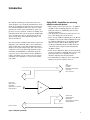
Agilent 8510C—Capabilities for measuring
amplifiers and active devices
• High output power at the test port (–15 dBm at
50 GHz for the 8517B Opt 007 test set) drives
high-power devices, eliminating the need for
external amplifiers.
• 0.02 dB power resolution provides precise control of the input power to the device.
• Power sweep (8 dB broadband, up to 26 dB narrowband for the 8510C with 8517B Opt 007 test
set, 1 dB broadband, up to 23 dB narrowband
with the 8515A, and 13 dB broadband, up to
23 dB narrowband with the 8514B) allows for
convenient gain compression measurements
(in dBm or mW).
• Power meter calibration improves measurement
accuracy and when combined with receiver calibration provides new capabilities such as
absolute output-power measurements.
• User-defined preset function saves setup time
and protects power-sensitive devices.
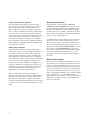
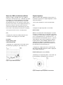
S21
Gain
Gain flatness
Gain drift
Deviation from linear phase
Group delay
Gain compression
S11
Input match
Input return loss
Input SWR
Input reflection coefficient
Input impedance
AUT
S22
Reverse isolation
Output match
Output return loss
Output SWR
Output reflection coefficient
Output impedance
S12
Figure 1. Amplifier parameters
3
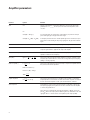
Amplifier parameters
Parameter
Equation
Definition
Gain
Vtrans
The ratio of the amplifier’s output power (delivered to a ZO load) to the input power
(delivered from a τ = ______ ZO source). ZO is the characteristic impedance, in this
case, 50 Ω.
Vinc
Gain (dB) = –20log10|τ|
For small signal levels, the output power of the amplifier is proportional to the input
power. Small signal gain is the gain in this linear region.
Gain (dB) = Pout (dBm) – Pin (dBm)
As the input power level increases and the amplifier approaches saturation, the output
power reaches a limit and the gain drops. Large signal gain is the gain in this nonlinear
region.
Gain flatness
The variation of the gain over the frequency range of the amplifier.
Reverse isolation
The measure of transmission from output to input. Similar to the gain measurement
except the signal stimulus is applied to the output of the amplifier.
Deviation from linear phase
The amount of variation from a linear phase shift. Ideally, the phase shift through an
amplifier is a linear function of frequency.
Group delay
Return loss (SWR, ρ)
tg(sec) = – ∆θ = – 1 * ∆θ
360 ∆f
∆ϖ
Γ=
Vrefl
= ρ∠θ
Vinc
The measure of the transit time through the amplifier as a function of frequency. A perfectly linear phase shift would have a constant rate of change with respect to frequency,
yielding a constant group delay.
The measure of the reflection mismatch at the input or output of the amplifier relative to
the system ZO characteristic impedance.
Reflection coefficient = ρ
Return loss (dB) = –20log10ρ
SWR =
Complex impedance
Gain compression
Z=
1+ρ
1–ρ
1+Γ
Z = R + jX
1–Γ * O
The amount of reflected energy from an amplifier is directly related to its impedance.
Complex impedance consists of both a resistive and a reactive component. It is derived
from the characteristic impedance of the system and the reflection coefficient.
An amplifier has a region of linear gain where the gain is independent of input power
level (small signal gain). As the power is increased to a level that causes the amplifier
to saturate, the gain decreases.
Gain compression is determined by measuring the amplifier’s 1 dB gain compression
point (P1dB) which is the output power at which the gain drops 1 dB relative to the small
signal gain. This is a common measure of an amplifier’s power output capability.
4
Measurement setup
Before making an actual measurement it is important to know the input and output power levels of
the AUT and the type of calibration required.
Setup
1. Select input power levels
Selecting the proper stimulus settings at the various ports of the AUT are of primary concern. If the
small signal gain and output power at the 1 dB
compression point of the amplifier are approximately known, the proper setting for the input
power level can be estimated. For linear operation,
the input power to the amplifier should be set such
that the output power is approximately 3 to 10 dB
below the 1 dB compression level.
Pinput (dBm) = P1dB compression(dBm)
– Gainsmall signal (dB)–10 dB
2. Estimate output power
It is also important to know the output power levels from the AUT to avoid overdriving or damaging
the test ports of the network analyzer. External
attenuation may be necessary after an AUT with
high output power to keep the power level below
the specified 0.1 dB compression level of the test
set. For more information see Appendix A, “Highpower measurements.”
When measuring high-gain amplifiers, it is possible
to overload the test port. Overload occurs when
greater than +17 dBm of power is input into either
port. When this happens, “IF OVERLOAD” will be
displayed. At this point, either more attenuation
should be added to the output of the amplifier, or
the input power level should be reduced before
continuing the measurement.
For the Agilent 8510C, the power may be varied
continuously within the “available output power
range” indicated in Table 1. If lower power is
required to the AUT, an internal step attenuator
may be varied from 10 to 90 dB in 10 dB steps. It
is advantageous to select a power range that will
accommodate the operation of the amplifier in its
linear region as well as the nonlinear region.
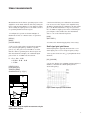
Table 1. Available output power from network analyzer
RF Source
8510 Test Set
83621A
with 8514B
83631A
with 8515A
Frequency (GHz)
0.05
2
20
26.5
40
50
83651A
with 8517B
83651A
with 8517B, Opt. 007
Test Port Power Levels (dBm)
+2.5 to –20.5
+1 to –22.0
–7.5 to –27
–3.5 to –26
–6 to –29
–13.5 to –30
–25 to –30
+1.5 to –21.5
+0.5 to –23.5
–7.5 to –30
–13.5 to –30
–20 to –30
–27 to –30
+5 to –21
+5 to –21
+2 to –23
+1 to –24
–3 to –21.5
–13 to –29
Table 2. Allowable input power to network analyzer
0.1 dB compression level for
test set (at test port) (dBm)
8514B at
20 GHz
8515A at
26.5 GHz
8517B at
50 GHz
+ 8.5
–3
–6
+17
+17
Damage power level at test port (dBm) +17
5
3. Power meter calibration (optional)
The 8510C network analyzer provides leveled
power at the test set port with a specified variation of less than 2.1 dB at 50 GHz. The power
meter calibration feature is available to provide
more accurate settable power when required and
can also serve to remove the frequency response
errors of the cables and adapters between the test
set and the AUT. If a power meter calibration is
performed it should be done prior to a measurement calibration. Power meter calibration with the
8510C family is compatible with the Agilent 437B
and 438A power meters.
4. Measurement calibration
A measurement calibration characterizes and
removes the effects of the repeatable variations (or
systematic errors) in the test setup. Systematic
errors include frequency response tracking, directivity, mismatch, and crosstalk effects. A full twoport calibration provides the greatest measurement
accuracy, but in some situations it may be more
practical to use other calibration techniques (i.e., a
response calibration for transmission-only measurements or a one-port calibration for reflectiononly measurements). For more information see
Appendix B, “Accuracy considerations.”
After a calibration has been performed, “C”
appears to the left of the display to indicate that a
measurement calibration is on. Any attenuation
that is used on the input or output of the AUT
should be included in the calibration of the system
to remove its effects from the measurement of the
AUT.
6
Operating considerations
If you perform a factory preset ([RECALL]
{MORE}{FACTORY PRESET}) the power is set to
the maximum leveled value (in the highest power
range) of +10 dBm. If the AUT could be damaged
by this power level or will be operating in its nonlinear region, it should not be connected until the
power is set to a desirable level.
A useful feature for the testing of power-sensitive
devices is the user preset feature on the 8510C.
This allows the user to specify an instrument setting for a particular measurement and to store it
away by pressing [SAVE] {USER PRESET 8}. Later,
when the green [USER PRESET] key is pressed,
these same conditions are recalled with the power
level and/or internal step attenuator set to the
appropriate level, preventing potential damage to
the AUT.
Measurement examples
The measurement examples described in this note
were made on an 8510C network analyzer with an
83651A source and 8517B Opt 007 test set. A full
two-port calibration was performed (except where
noted) for the greatest accuracy for both transmission and reflection measurements of the two-port
device. The amplifier under test is an 8348A amplifier operating over a 2 to 26.5 GHz frequency
range. Other sources and test sets may be used, but
differences in frequency range and available output power will exist.
Linear measurements
Measurements in the linear operating region of the
amplifier can be made with the 8510C by using the
basic setup shown in Figure 2. Care must be taken
when setting the input power to the AUT so that it
is operating within its linear region.
1. Configure the system as shown in Figure 2.
Return the 8510C to a known state of operation.
3. Perform a full two-port calibration. If attenuators are used on the output of the amplifier they
should be included in the calibration. In this example, a 20 dB fixed attenuator on port 2 prevents
the +25 dBm of output power from overdriving the
port 2 input of the 8517B. Save the instrument
state to one of the internal registers.
[SAVE]
{INST STATE 1}
[RECALL]
[MORE]
[FACTORY PRESET]
4. Connect the AUT and apply bias, if necessary.
2. Choose the appropriate measurement parameters (start/stop frequency, number of points,
power, etc). The power level should be set such
that the AUT is operating in its linear region. In
this measurement example, an estimated input
power level of –15 dBm is derived from:
Small signal gain/gain flatness
Pin = P1dB – Gain – 10 dB
= +25 dBm – 30 dB – 10 dB
= –15 dBm
[S21] [LOG MAG]
[START] [2] [G/n]
[STOP] [26.5] [G/n]
STIMULUS [MENU]
{POWER SOURCE 1} [–15] [x1]
Attenuator
(if needed)
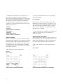
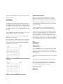
Small signal gain is typically measured at a constant input power over a swept frequency range.
1. Set up the 8510C for an S21 log magnitude measurement.
2. Scale the display for optimum viewing and use a
marker to measure the small signal gain at a
desired frequency.
Figure 3. Small signal gain measurement
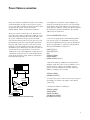
AUT
Thru
Open
Short
Load
Figure 2. Basic setup for amplifier measurement using the
8510C network analyzer
7
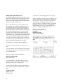
3. Measure the gain flatness or variation over a
frequency range using the following sequence.
First, set the appropriate start/stop or center/span
frequencies over which the flatness is to be measured. Then perform an appropriate calibration
over this frequency range. Then perform the following to see a direct readout of the peak-to-peak
difference in the trace.
[MARKER]
{MARKER 1}
{MORE} {MARKER TO MINIMUM}
[PRIOR MENU]
{MARKER 2}
{MODE MENU} {REF=1}
{MORE} {MARKER TO MAXIMUM}
2. Set up the Agilent 8510C for an S12 log magnitude measurement.
[S12] [LOG MAG]
If the isolation of the AUT is very high (i.e., displayed trace is in the noise floor) it may be necessary to remove the external attenuation at the output of the AUT and recalibrate (with a response
and isolation calibration) at a higher power level
and increased averaging.
3. Scale the display for optimum viewing and use a
marker to measure the reverse isolation at a
desired frequency.
Deviation from linear phase
Reverse isolation
For the measurement of reverse isolation the RF
stimulus signal is applied to the output of the AUT
by measuring S12. External attenuation placed on
the output of the AUT may not be needed for this
measurement since the signal path now exhibits
loss instead of gain. If it is removed, a new calibration will be required.
The measurement of deviation from linear phase of
the AUT employs the electrical delay feature of the
8510C network analyzer to remove the linear portion of the phase shift from the measurement.
1. Set up the analyzer for an S21 phase measurement.
[S21] [PHASE]
1. Recall the full two-port calibration.
[RECALL]
{INST STATE 1}
Figure 4. Reverse isolation measurement
8
Figure 5. Deviation from linear phase measurement
2. Place a marker in the center of the band and
activate the electrical delay feature,
[MARKER] {MARKER 1} {12 GHz}
RESPONSE [MENU]
{COAXIAL} OR {WAVEGUIDE}
depending upon whether the media exhibits intrinsic linear or dispersive phase shift.
{AUTO DELAY}
3. {ELECTRICAL DELAY} is now the active function.
Use the knob, STEP keys, or numeric and units
to fine tune the electrical delay for a flat phase
response near the center of the passband. The
linear phase shift through the AUT is effectively
removed and all that remains is the deviation
from this linear phase shift.
Group delay
Group delay is calculated from the phase and frequency information and is displayed in real time
by the 8510C network analyzer.
1. Set up the 8510C for an S21 group delay measurement.
[S21] [DELAY]
2. Activate a marker to measure the group delay at
a particular frequency.
Group delay measurements may require a specific
aperture (∆f) or frequency spacing between measurement points. The phase shift between two adjacent frequency points must be less than 180°, otherwise incorrect group delay information may
result.
number of points – 1
2 * (frequency span)
4. Use the markers to measure the maximum peakto-peak deviation from linear phase.
Approximate delay of AUT <
[MARKER]
{MARKER 1}
{MORE} {MARKER TO MINIMUM}
[PRIOR MENU]
{MARKER 2}
{MODE MENU} {REF=1}
{MORE} {MARKER TO MAXIMUM}
The effective group delay aperture can be
increased from the minimum by varying the
smoothing percentage. Increasing the aperture
reduces the resolution demands on the phase
detector and permits better group delay resolution
by increasing the number of measurement points
over which the group delay aperture is calculated.
Since increasing the aperture removes fine grain
variations from the response, it is critical that
group delay aperture be specified when comparing
group delay measurements. To adjust the aperture
press RESPONSE [MENU] [SMOOTHING ON] and
adjust aperture as necessary.
Figure 6. Group delay measurement with minimum and
increased aperture
9
Return loss, SWR, and reflection coefficient
Complex impedance
Return loss (RL), standing wave ratio (SWR) or
reflection coefficient (rho) are commonly specified
to quantify the reflection mismatch at the input
and output ports of an AUT. Because reflection
measurements involve loss instead of gain, power
levels are lower at the receiver inputs. Therefore, it
may be necessary to increase power levels for
reflection measurements. Alternatively, the noise
levels can be reduced by increasing the averaging.
When the phase and magnitude characteristics of
an AUT are desired, the complex impedance can be
easily determined.
1. Set up the 8510C for an S11 measurement.
[SMITH CHART]
[S11]
Markers used with this format display R + jX. The
reactance is displayed as an equivalent capacitance
or inductance at the marker frequency. Marker values are normally based on a system ZO of 50 Ω. If
the measurement environment is not 50 Ω, the network analyzer characteristic impedance must be
modified under [CAL] {MORE} {SET Z0} before
calibrating. In addition, a minimum loss pad or
matching transformer must be inserted between
the AUT and the measurement port.
2. Display the return loss, SWR, and reflection
coefficient of the input port of the AUT.
[LOG MAG]
FORMAT [MENU] {SWR}
{LINEAR MAGNITUDE}
3. Similarly, the output match of the AUT can be
measured by repeating the procedure for S22.
1. Set up the analyzer for an S11 measurement.
[S11]
2. Display the input impedance of the AUT.
3. Display the complex reflection coefficient (G).
The linear magnitude and phase will be displayed
at the marker frequency.
FORMAT [MENU] {Re/Im mkr on POLAR}
4. Similarly, the output impedance of the AUT can
be measured by repeating the process for S22.
Figure 7. Input SWR measurement
Figure 8. Complex output impedance measurement
10
Power flatness correction
The power flatness calibration feature of the 8510C
network analyzer provides a more precise power
level to the AUT. A 437B or 438A power meter and
an appropriate power sensor such as the
Agilent 8481A, 8485A or 8487A are required.
The power sensor is attached to the desired test
port, after any cables or adapters leading up to the
point where the AUT will be connected, and a single power calibration sweep is performed. The
power meter monitors the test port power at each
measurement point across the frequency band of
interest, and a table of power corrections versus
frequency is derived and stored in the 8360 synthesized sweeper. When the power meter is disconnected and the test port flatness correction is
enabled, the source will adjust the output power to
compensate for path losses at each measurement
point in the frequency span, with no degradation
in measurement speed.
1. Configure the system as shown in Figure 10.
Connect the 437B power meter to the system bus
of the 8510C. Zero and calibrate the power meter.
Verify that the address of the power meter matches
the setting in the network analyzer. The default
address for the 437B is 13.
[LOCAL] {POWERMETER} [13] [x1]
2. Choose the appropriate measurement parameters. Set the source to maximum leveled power
(P1) at the highest frequency in the measurement
span. See Appendix C, “8360 Series Synthesized
Sweepers maximum leveled power.”
[START] [2] [G/n]
[STOP] [26.5] [G/n]
[S21]
STIMULUS [MENU]
{POWER MENU}
{POWER SOURCE 1}P1 [x1]
3. When the flatness calibration is initiated, the
analyzer sends the source a list of flatness correction frequencies equal to the number of trace
points set on the analyzer. If needed, adjust the
number of analyzer trace points.
8510 System Bus
STIMULUS [MENU]
{NUMBER of POINTS}
Attenuator
(if needed)
AUT
8485A
Power sensor
437B
Power Meter
Figure 9. Power flatness correction setup
4. Connect the power sensor to the active test port
(normally port 1 where the input of the AUT is
connected).
5. Initiate the flatness calibration.
STIMULUS [MENU]
{POWER MENU}
{POWER FLATNESS}
{CALIBRATE FLATNESS}
{FLATNESS CAL START}
11
6. When the calibration is complete, activate flatness correction.
[PRIOR MENU]
{FLATNESS ON}
7. Verify the constant power level at the test port
by using the 437B to measure the test port power
at CW frequencies. As the power is manually measured, the user must enter each test frequency on
the 437B so that the correct calibration factor will
be used.
8. The analyzer will automatically store the correction table into register 1 of the source.
9. Remove the power sensor. Connect AUT and
apply bias, if necessary.
Once the flatness calibration has been completed
the user may choose to reduce the measurement
frequency span at any time without invalidating
the flatness correction.
Absolute output power
After port 1 has been calibrated for a constant
input power, the 8510C can be used to display
absolute power (in dBm or mW) versus frequency.
1. Perform a power flatness correction over the
desired frequency range and power level (as previously described).
2. Set up channel 1 for the desired frequency
range, number of points and step sweep mode.
3. Set the source power at a value appropriate for
the device under test. This step is necessary to get
a correct reading of absolute power. Connect a
thru and perform a receiver calibration to remove
the frequency response errors of the port 2 path in
the measurement. Be sure to include any attenuators or adapters which are part of the measurement.
[CAL]
{RECEIVER CAL}
{INPUT PWR}
{OUTPUT PWR}
{SAVE RCVR CAL}
If several THRU’s have been defined in the calibration kit, a further menu appears after {OUTPUT
PWR} is selected to allow selection of the appropriate standard.
A flat line should be displayed at the correct power
level.
Figure 10. Test port power before and after a power meter
calibration
4. Connect the AUT and apply bias, if necessary.
5. When Receiver Cal is turned on, parameter
User 1 a1 displays input power (Pin) in dBm and
User 2 b2 displays output power (Pout).
PARAMETER [MENU]
{USER 1 a1}
{USER 2 b2}
Figure 11. Absolute output power measurement
12
Nonlinear measurements
The Agilent 8510C has the capability to make
measurements of amplifiers operating in their nonlinear region. A swept-frequency gain compression
measurement locates the frequency at which the
1 dB gain compression first occurs. A swept-power
gain compression measurement shows the reduction in gain at a single frequency as a power ramp
is applied to the AUT.
Swept-frequency gain compression
A measurement of swept-frequency gain compression locates the frequency at which the 1 dB gain
compression first occurs. The swept-frequency gain
compression is determined by normalizing to the
small signal gain and by observing compression as
the 1 dB drop from the reference line as input
power is increased. The swept-frequency gain compression and corresponding output power (P1dB)
can be displayed simultaneously on the 8510C network analyzer.
1. Perform an absolute output power calibration
and measurement (as previously described).
2. Channel 1 should already be set up for an
absolute power measurement (with correction on).
Set up channel 2 for an S21 gain measurement.
Turn on a dual channel split display.
5. Set a scale of 0.5 dB/division and a reference
value of 0 dB to allow easy viewing of a 1 dB drop
from the small signal gain.
6. Increase the source power level until the trace
drops by 1 dB at some frequency. A marker can
then be used to read the exact frequency where the
1 dB compression first occurs. Care should be
taken when increasing the source power so that
the input power limitation of the AUT is not
exceeded.
STIMULUS [MENU]
{POWER MENU} {POWER SOURCE 1}
Use knob or arrow keys to increase power.
[MARKER]
{MARKER 1}
7. Set the source power on channel 1 to the same
value as for channel 2. The channel 1 marker displays the actual output power of the amplifier (in
dBm) at the 1 dB gain compression point. In this
example, the 1 dB gain compression first occurs at
26.255 GHz at an output power level of 16.19 dBm.
[CH 2] [S21]
[LOG MAG]
[DISPLAY] {DISPLAY MODE}
{DUAL CHAN SPLIT}
3. Connect the AUT and apply bias, if necessary.
4. Normalize the display to the small signal gain.
[DISPLAY] {DATA AND MEMORIES}
{DATA->MEMORY}
{Math (/)}
Figure 12. Swept-frequency gain compression measurement
A flat line at 0 dB should now be displayed on
channel 2.
13
Swept-power gain compression
By applying a fixed-frequency power sweep to the
input of an amplifier, the gain compression can be
observed as a 1 dB drop from small signal gain.
The power sweep should be selected such that the
AUT is forced into compression.
The S21 gain will decrease as the input power is
increased into the nonlinear operating region of
the amplifier. The 8510C network analyzer has a
power sweep range as defined earlier in Table 1.
The fixed frequency chosen could be the frequency
for which the 1 dB drop first occurs in a sweptfrequency gain compression measurement. The
swept-power gain compression and corresponding
output power (Pout) can be displayed simultaneously
on the 8510C network analyzer. A power flatness
correction over a power sweep range (at a fixed
frequency) may be performed first if very accurate
power is required at the input to the AUT.
7. Connect the AUT and apply bias, if necessary.
8. Move a marker to the flat portion of the trace. If
there is no flat portion the AUT is in compression
throughout the sweep, and power levels must be
decreased. Use the marker search to find the
power for which a 1 dB drop in gain occurs. Read
the marker value for channel 1 to determine the
absolute input power (Pin) or output power (Pout)
where the 1 dB gain compression occurs.
[MARKER] {MORE} {MINIMUM}
[CHANNEL 1]
PARAMETER [MENU]
{USER 1 a1} or {USER 2 b2}
In this example, the 1 dB gain compression at
26.255 GHz occurs at an output power level of
16.006 dBm and an input power level of –14.7
dBm.
1. Configure the system as shown in Figure 2.
2. Perform a power flatness correction, if necessary.
3. Set up channel 1 for an absolute power measurement and channel 2 for an S21 gain measurement
as described earlier.
4. Turn on a dual channel split display.
[DISPLAY] {DISPLAY MODE}
{DUAL CHAN SPLIT}
5. Set the marker to the CW frequency point of
interest, and set the power low enough to avoid
driving the device into compression.
6. Turn on power domain. Set the start and stop
power points to drive the amplifier into compression.
[DOMAIN] {POWER}
[START] –22 [x1]
[STOP] –12 [x1]
14
Figure 13. Swept power gain compression measurement
Appendix A—High-power measurements
Custom test set configurations
Special test set configurations
The Agilent 85110 test set provides the greatest
flexibility for the testing of high-power amplifiers
which often require custom test set configurations.
The 85110 test set is an open architecture which
allows amplifiers to be added to the RF path of
the test set. External test set components (amplifiers, couplers, isolators, attenuators, etc.) can be
specially selected to provide the necessary power
handling capability.
Special 8510 test set configurations for high-power
testing are available on a request basis. An example of a special 85110 configuration is shown in
Figure 15. This modified RF block diagram allows
up to 500 watts (CW) of high-power handling capability and also provides the ability to connect additional test equipment to the AUT via a single RF
connection.
For example, if the required input power for the
AUT is greater than the standard 8510C test set
can provide, the 85110 test set allows the addition
of an amplifier to properly drive the AUT. Highpower couplers and attenuators are required to
prevent over-driving the reference and test samplers.
High-power directional couplers replace the standard directional couplers in the 85110. A pair of
high-power step attenuators are added before the
test samplers (A and B) to prevent them from
being overdriven by the AUT. For some amplifier
measurements, throughput is a major concern due
to the multiplicity of tests that are required. It is
desirable to make as many measurements as possible at one test station with a single connection to
the device to reduce lengthy setup time. The front
panel port 1 and port 2 jumpers also allow the
addition of other test equipment (power meter,
spectrum analyzer, noise figure meter, etc.) for a
single connection multiple measurement solution.
15
Jumper
Jumper
RF input
High
Power
Load
▲
▲
▲
▲
▲
Port 2
▲
▲
▲
▲
Four
way
splitter
▲
▲
▲
▲
▲
▲
▲
▲
▲
(5 Watts Port Power)
▲
▲
▲
Port 1
▲
▲
▲
30 dB
Couplers
▲
▲
Figure 14. 85110 simplified block diagram
▲
Port 1
Port 2
(Safely handles 500 watts CW or 5 KW peak)
Figure 15. Block diagram for special high-power test set
configuration for the 85110
16
Peak
Power
Meter
▲
–16 dB
▲
Fundamental
mixers
Spec
An
▲
b2
▲
Step
atten
▲
b1
▲
a2
▲
▲
RF input
▲
▲
a1
▲
▲
▲
▲
▲
▲
–16 dB
LO input
▲
▲
Step
atten
▲
Four
way
splitter
▲
▲
▲
▲
Solid state
PIN switch
LO input
Appendix B—Accuracy considerations
Error correction can be applied to the measurements discussed in this note to reduce the measurement uncertainty. A full two-port calibration
was used for the measurement examples (except
where noted) to provide the best measurement
accuracy of both transmission and reflection measurements of two-port devices. When a full two-port
calibration is applied, the dynamic range and accuracy of the measurement is limited only by the system noise and stability, connector repeatability,
and the accuracy to which the characteristics of
the calibration standards are known.
In some instances it may be more convenient to
perform a response calibration to remove the frequency response errors of the test setup for transmission only measurements when extreme accuracy is not a critical factor. Likewise, an S11 one-port
or S22 one-port calibration to remove directivity,
source match and frequency response errors may
be more convenient for reflection only measurements when the AUT is well-terminated.
Transmission measurements
For a gain measurement, the three major sources
of error are the frequency response error of the
test setup, the source and load mismatch error
during the measurement, and the dynamic accuracy.
A simple response calibration using a thru connection significantly reduces the frequency response
error which is usually the dominant error in a
transmission measurement. For the greatest accuracy, a full two-port calibration can be used which
also reduces the uncertainty in the measurement
caused by the source and load match.
Dynamic accuracy is a measure of the receiver’s
performance as a function of the incident power
level and has an effect on the uncertainty of a gain
measurement. This is because the receiver detects
a different power level between calibration and
measurement. The effects of dynamic accuracy on
a gain measurement are negligible (less than 0.5 dB)
as long as the network analyzer is operating below
the specified 0.1 dB compression level.
A gain drift measurement is subject to the same
errors as a gain measurement. Another factor that
could be significant is the transmission tracking
drift of the system. This drift is primarily caused
by the change in the temperature of the test setup
between calibration and measurement. To minimize this effect, allow the instrument to stabilize to
the ambient temperature before calibration and
measurement.
A reverse isolation measurement is subject to the
same errors as a gain measurement. In addition, if
the isolation of the AUT is very large, the transmitted signal level may be near the noise floor or
crosstalk level of the receiver. To lower the noise
floor, a decreased IF bandwidth may be necessary.
When crosstalk levels begin to affect the measurement accuracy, a response and isolation calibration
or a full two-port calibration (including the isolation part of the calibration) removes the crosstalk
error term. When performing the isolation part of
the calibration it is important to use the same
averaging factor and IF bandwidth during the calibration and measurement.
For deviation from linear phase measurements, the
phase uncertainty is calculated from a comparison
of the magnitude uncertainty (already discussed
for gain measurements) with the test signal magnitude.
17
Reflection measurements
The uncertainty of a reflection measurement such
as return loss, SWR, reflection coefficient and
impedance is affected by directivity, source match,
load match, and reflection tracking of the test system. With a full two-port calibration, the effects of
these factors are minimized. A one-port calibration
can provide equivalent results if the amplifier has
sufficient isolation to reduce the effects of the load
match.
Nonlinear measurements
For absolute power measurements, a frequency
response calibration is used. Because the power
calibration is made relative to 50 Ω, inaccuracies
due to mismatch will occur when a device is
attached that is not exactly 50 Ω. Since the power
meter calibration feature is not a true leveling feature, it cannot correct for mismatches that occur
between the test port and the AUT. Mismatch can
be reduced by using attenuators at the input or
output of the AUT.
For a gain compression measurement a response
calibration reduces the frequency response errors.
A gain compression measurement requires the
power level to be changed after a calibration. The
Agilent 8360 Series sources, used with the 8510C
are specified to have a source linearity of ±.5 dB,
typically less then ±.2 dB. Source linearity uncertainty can be reduced by performing a power flatness correction at the input of the AUT. This precisely sets the power level incident to the AUT by
compensating the source power for any nonlinearities in the source or test setup.
18
Appendix C—8360 series synthesized sweepers maximum
leveled power (dBm)
Frequency
83620A/
83621A
83623A
83631A
83651A
20 GHz
26.5 GHz
40 GHz
50 GHz
+10
—
—
—
+17
—
—
—
+10
+4
—
—
+10
+4
+3
0
When power levels from the AUT are such that
external attenuation is not practical or when the
source cannot deliver enough power to properly
drive the AUT, it may be necessary to construct a
custom test set.
19
Appendix D—Optimizing power sweep range
Power sweep range will be reduced if a power flatness correction is used in combination with power
sweep. If flat test port power is required, there is
no way to avoid this.
If the source has step attenuators installed, and a
power flatness correction is used with power
sweep, the available sweep range will be further
reduced. This reduction is due to the source setting
the attenuator for the optimum ALC (automatic
leveling control) range. This loss in sweep range
can be compensated for using one of the following
two methods. Both methods require a computer to
implement a work around which allows better use
of the ALC range in the 8360 synthesizer when
using power sweep plus flatness correction.
The second method involves connecting the computer to the 8510 and using the “pass-through”
address to access the source. Pass-through allows
you to WRITE to the source, but not READ them
from the source, so an alternate method must be
used.
Since you can’t read the actual array from the
8510, you have to find another way to get the same
data. With the 8510, you can read the power to the
test port by looking at “a1” instead of S11, S21, etc.
The procedure is as follows.
1. Read the “a1” data with flatness off into a computer.
2. Read the “a1” data with flatness on.
The first method involves using a computer connected directly to the source to make the modifications.
1. Read the flatness correction array from the
8360. Determine the average.
2. Determine the average amplitude correction the
array is providing (max+min)/2 (eg. (–10 dBm +
–30 dBm)/2).
3. Calculate the difference in dB between the two
traces and determine the max and min correction.
From that, calculate the “average correction.”
4. Build a new flatness array, subtracting the “average correction” as in the previous process.
5. Write this to the 8360 using pass-through.
6. Set the power offset also using pass-through.
3. Subtract this number from each of the numbers
in the array and put this modified array back into
the 8360.
4. Use that same “average correction” and input
that as a “power offset”.
The net result will be the same power out of the
8360, but the attenuators will be “faked out” and
allow as much of the ALC range to be used as possible. (Remember that some sweep range will still
be lost because of the flatness correction.)
20
Note: You must make sure you are operating in the
linear region of the test set, otherwise the offset
will not be correct.
The following example program demonstrates this
method.
350
360
10
20
30
370
380
40
50
60
70
80
90
100
110
120
130
140
150
160
170
180
190
200
210
220
230
240
250
260
270
280
290
300
310
320
330
340
! RE-SAVE “POW_OFFSET”
!
! This program calculates and removes the average
amplitude correction
! factor from the 8360 flatness correction array. It
then sets and
! activates this average amplitude as a constant offset to the 8360
! power output. The flatness array minus the offset is
then re-written
! to the 8360. The net result output power is the
same (flat test port
! power). However, full ALC range will now be avalible for any power
! or attenuator setting.
!
DIMDiff(1:801,1),Flat_on(1:801,1), Flat_off(1:801,1)
INTEGER I,Preamble,Bytes
ASSIGN @Na TO 716
ASSIGN @Na_data TO 716;FORMAT OFF
ASSIGN @Na_sys TO 717
CLEAR SCREEN
!
PRINT TABXY(0,5)
PRINT “NOTICE:”
PRINT
PRINT “This program will only work in STEP or
RAMP sweep modes. Any”
PRINT “number of points may be used (51, 101, 201,
401 or 801).”
PRINT
PRINT “A test port power flatness calibration must
already be done.”
PRINT
PRINT “The current instrument state will be saved in
Inst State 5 and”
PRINT “recalled at the end of this program.”
INPUT “Press <Return> to continue.”,In$
CLEAR SCREEN
OUTPUT @Na;”SAVE5”
GOSUB Get_data
GOSUB Process_data
OUTPUT @Na;”RECA5; FLATON”
!
390
400
410
420
430
440
450
460
470
480
490
500
510
520
530
540
550
560
570
580
590
600
610
620
630
640
650
660
670
680
690
PRINT TABXY(0,5)
PRINT “Source PowerOffset=”;PROUND (Offset,–2);”
db”
PRINT
PRINT “WARNING: Power offset is now on in the
source. This offset is”
PRINT “applied to the power setting displayed by the
8510 with flatness”
PRINT “turned On OR Off.”
PRINT “Power offset will be turned off in the source
if a factory”
PRINT “preset is executed OR 8510 power is
cycled. Otherwise it will”
PRINT “be applied.”
PRINT “Flatness data stored in the source is only
valid with offset”
PRINT “on. You must re-do 8510 flatness calibration
(without offset)”
PRINT “before running this program again for correct
results.”
DISP “Program Complete”
LOCAL @Na
STOP
!
Get_data: !
OUTPUT @Na;”USER1; LOGM; AVERON 64; FLATON;
SING”
OUTPUT @Na;”FORM3; OUTPFORM”
ENTER @Na_data;Preamble,Bytes
REDIMDiff(1:Bytes/16,1),Flat_on (1:Bytes/16,1),
Flat_off(1:Bytes/16,1)
ENTER @Na_data;Flat_on(*) ! Flat_on(*,0) = amplitude db
! Flat_on(*,1) = 0
OUTPUT @Na;”FLATOFF; SING; FORM3; OUTPFORM”
ENTER
@Na_data;Preamble,Bytes,Flat_off(*) ! Flat_off (*,0) =
amplitude db
! Flat_off(*,1) = 0
OUTPUT @Na;”POIN; OUTPACTI”
ENTER @Na;Points
OUTPUT @Na;”STAR; OUTPACTI”
ENTER @Na;Start_freq
OUTPUT @Na;”STOP; OUTPACTI”
ENTER @Na;Stop_freq
RETURN
!
Process_data: !
21
700
710
720
730
740
750
760
770
780
790
800
810
820
830
840
850
860
870
880
890
900
910
920
930
940
950
MAT Diff= Flat_on-Flat_off ! Diff(*) = source flatness
corr array
Offset=SUM(Diff)/(Bytes/16)
MAT Diff(*,1)= Diff(*,0) ! Diff(*,1) = flatness amplitudes
Freq_increment=(Stop_freqStart_freq)/
(Points-1)
Freq=Start_freq
FOR I=1 TO Points
Diff(I,0)=Freq ! Diff(*,0) = flatness frequencies
Diff(I,1)=Diff(I,1)-Offset ! remove offset from flatness
amplitudes
Freq=Freq+Freq_increment ! next frequency
NEXT I
OUTPUT @Na;”ADDRPASS 19”
OUTPUT @Na_sys;”SYST:LANG TMSL”
WAIT 3
OUTPUT @Na_sys ! required after 8360 language
switch, ignore system
! bus address error.
OUTPUT @Na_sys;”CORR:FLAT “;Diff(*) ! output
modified flatness array
OUTPUT @Na_sys;”POW:OFFS “;Offset
OUTPUT @Na_sys;”POW:OFFS:STAT ON”
OUTPUT @Na_sys;”SYST:LANG COMP”
WAIT 1
OUTPUT @Na;”ADDRPASS 31; CONT; POWE; OUTPACTI”
ENTER @Na;Power
OUTPUT @Na;”POWE “;Power ! must resend power
so source applies offset
RETURN
!
END
Agilent Technologies’ Test and Measurement
Support, Services, and Assistance
Agilent Technologies aims to maximize the value you receive,
while minimizing your risk and problems. We strive to ensure
that you get the test and measurement capabilities you paid
for and obtain the support you need. Our extensive support
resources and services can help you choose the right Agilent
products for your applications and apply them successfully.
Every instrument and system we sell has a global warranty.
Support is available for at least five years beyond the production life of the product. Two concepts underlie Agilent’s
overall support policy: “Our Promise” and “Your Advantage.”
Our Promise
“Our Promise” means your Agilent test and measurement equipment will meet its advertised performance and functionality.
When you are choosing new equipment, we will help you with
product information, including realistic performance specifications and practical recommendations from experienced test
engineers. When you use Agilent equipment, we can verify that
it works properly, help with product operation, and provide
basic measurement assistance for the use of specified capabilities, at no extra cost upon request. Many self-help tools are
available.
Your Advantage
“Your Advantage” means that Agilent offers a wide range of
additional expert test and measurement services, which you
can purchase according to your unique technical and business
needs. Solve problems efficiently and gain a competitive edge
by contracting with us for calibration, extra-cost upgrades, outof-warranty repairs, and on-site education and training, as well
as design, system integration, project management, and other
professional services. Experienced Agilent engineers and technicians worldwide can help you maximize your productivity,
optimize the return on investment of your Agilent instruments
and systems, and obtain dependable measurement accuracy
for the life of those products.
Get assistance with all your test and measurement needs at:
www.agilent.com/find/assist
Product specifications and descriptions in this
document subject to change without notice.
Copyright © 1994, 2000 Agilent Technologies
Printed in U.S.A. 9/00
5963-2352E