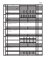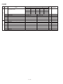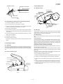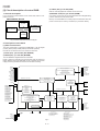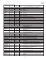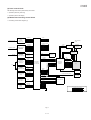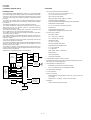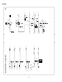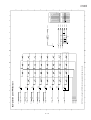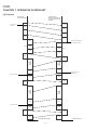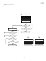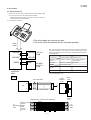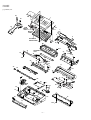
1
UX-40DE
FO-50DE
SERVICE MANUAL
No. 00ZUX40DE/SME
FACSIMILE
MODEL
UX-40
FO-50
Illustration: UX-40
CONTENTS
CHAPTER 1. GENERAL DESCRIPTION
[1] Specifications ............................................
[2] Operation panel .........................................
[3] Transmittable documents ..........................
[4] Installation .................................................
[5] Quick reference guide ...............................
1-1
1-2
1-3
1-4
1-8
CHAPTER 2. ADJUSTMENTS
[1] Adjustments .............................................. 2-1
[2] Diagnostics and service soft switch .......... 2-2
[3] Troubleshooting ...................................... 2-18
[4] Error code table ....................................... 2-19
CHAPTER 3. MECHANISM BLOCKS
[1] General description ................................... 3-1
[2] Disassembly and assembly
procedures ....................................... 3-3
CHAPTER 4. DIAGRAMS
[1] Block diagram ............................................4-1
[2] Wiring diagram .......................................... 4-2
[3] Point-to-point diagram ............................... 4-3
CHAPTER 5. CIRCUIT DESCRIPTION
[1] Circuit description ..................................... 5-1
[2] Circuit description of control PWB ............ 5-2
[3] Circuit description of TEL/LIU PWB .......... 5-9
[4] Circuit description of
power supply PWB ............................5-12
[5] Circuit description of CIS unit ...................5-12
CHAPTER 6. CIRCUIT SCHEMATICS AND
PARTS LAYOUT
[1] Control PWB circuit ................................... 6-1
[2] TEL/LIU PWB circuit .................................. 6-9
[3] Power supply PWB circuit ...................... 6-13
[4] Operation panel PWB circuit ................... 6-15
CHAPTER 7. OPERATION FLOWCHART
[1] Protocol ..................................................... 7-1
[2] Power on sequence ................................... 7-2
CHAPTER 8. OTHERS
[1] Service tools ............................................. 8-1
[2] IC signal name .......................................... 8-4
PARTS GUIDE
Parts marked with " " is important for maintaining the safety of the set. Be sure to replace these parts with specified ones for
maintaining the safety and performance of the set.
SHARP CORPORATION
This document has been published to be used
for after sales service only.
The contents are subject to change without notice.
UX-40DE
FO-50DE
CAUTION FOR BATTERY REPLACEMENT
(Danish)
ADVARSEL !
Lithiumbatteri-Eksplosionsfare ved fejlagtig håndtering.
Udskiftning må kun ske med batteri af samme fabrikat og type.
Levér det brugte batteri tilbage til leverandoren.
(English)
Caution !
Danger of explosion if battery is incorrectly replaced.
Replace only with the same or equivalent type
recommended by the equipment manufacturer.
Discard used batteries according to manufacturer’s
instructions.
(Finnish)
VAROITUS
Paristo voi räjähtää, jos se on virheellisesti asennettu.
Vaihda paristo ainoastaan laitevalmistajan suosittelemaan
tyyppiin. Hävitä käytetty paristo valmistajan ohjeiden
mukaisesti.
(French)
ATTENTION
Il y a danger d’explosion s’ il y a remplacement incorrect
de la batterie. Remplacer uniquement avec une batterie du
même type ou d’un type recommandé par le constructeur.
Mettre au rébut les batteries usagées conformément aux
instructions du fabricant.
(Swedish)
VARNING
Explosionsfare vid felaktigt batteribyte.
Använd samma batterityp eller en ekvivalent
typ som rekommenderas av apparattillverkaren.
Kassera använt batteri enligt fabrikantens
instruktion.
(German)
Achtung
Explosionsgefahr bei Verwendung inkorrekter Batterien.
Als Ersatzbatterien dürfen nur Batterien vom gleichen Typ oder
vom Hersteller empfohlene Batterien verwendet werden.
Entsorgung der gebrauchten Batterien nur nach den vom
Hersteller angegebenen Anweisungen.
UX-40DE
FO-50DE
CHAPTER 1. GENERAL DESCRIPTION
[1] Specifications
Automatic dialing:
Rapid Key Dialing: 5 numbers
Speed Dialing: 35 numbers
Fax(thermal) paper:
Initial starter roll (included with machine):
10 m
Recommended replacement roll:
FO-20PR, 30m
Modem speed:
9600 bps with automatic fallback to lower
speeds
Transmission time* :
Approx. 15 seconds
Resolution:
Horizontal: 8 dots/mm
Vertical:
Standard: 3.85 lines/mm
Fine/Halftone: 7.7 lines/mm
Super fine: 15.4 lines/mm
Automatic document feeder: 5 pages max. (80 g/cm2 paper)
Halftone (grayscale):
64 levels
Display:
16-digit LCD display
Compression scheme:
MR, MH, Sharp (H2)
Applicable telephone line:
Public switched telephone network/PBX
Compatibility:
ITU-T (CCITT) G3 mode
Input document size:
Automatic feeding:
Width: 148 to 216 mm
Length: 140 to 297 mm
Manual feeding:
Width: 148 to 216 mm
Length: 140 to 600 mm
Effective scanning width:
210 mm max.
Effective printing width:
210 mm max.
Contrast control:
Automatic/Dark selectable
Reception modes:
Fax, Tel, Fax/Tel
Copy function:
Yes
Noise emission:
Less than 70 dBA (Measured according to DIN 45 635)
Telephone function:
Yes (cannot be used if power fails)
Power requirements:
220-230 V AC, 50 Hz
Operating temperature:
5 - 35°C
Humidity:
Maximum: 85 % RH
Power consumption:
Standby: 2.3 W
Maximum: 115 W
Dimensions:
Width: 304 mm
Depth: 236 mm
Height: 122 mm
Weight:
Approx. 2.6 kg
* Based on ITU-T (CCITT) Test Chart #1 at standard resolution in Sharp
special mode, excluding time for protocol signals (i.e., ITU-T phase C
time only).
Note: The facsimile machine is Year 2000 compliant.
As a part of our policy of continuous improvement, SHARP reserves the right to make design and specification changes for procduct
improvement without prior notice. The performance specifications figures indicated are nominal values of production units. There may be some
deviation from these values in individual units.
1–1
UX-40DE
FO-50DE
[2] Operation panel
12
3 4
RECEPTION
MODE FUNCTION
TEL FAX
TEL
6 7
5
RESOLUTION
FAX
DOWN
VOLUME
UP
A.M.
TEL/FAX ANRUFB.
ABC
1
DEF
ABC
SPEED DIAL
A
GHI
JKL
C
B
D
STOP
REDIAL
03
04
PQRS
05
06
07
08
FUNKTION
PQRS
TUV
WXYZ
KOPIE/
HILFE
HOLD/SEARCH
START
2
4
MNO
AUFLÖSUNG/
EMPFANGSART
DEF
JKL
GHI
LAUTSTÄRKE
01
02
E/
ABRUF
2
7
KURZWAHL
3STOP
MNO
5
6
WXYZ
TUV
WAHLWDH.
COPY/HELP
8
9
SYMBOLE
0 START
ALPHAWAHL
R
LAUTSPR.
SPEAKER
09
8
9
1. Zielwahltasten (Rapid Dial keys)
10 11
When a document is in the feeder, press this key to make
a copy of a document. At any other time, press this key to
print out the Help List, a quick reference guide to the
opeation of your fax machine.
2. LCD-Anzeige (Display)
This displays messages and prompts during operation and
programming.
Press this key to select various special functions.
11. Taste AUFLÖSUNG/EMPFANGSART
(RESOLUTION/RECEPTION MODE key)
When a document is in the feeder, press this key to adjust
the resolution for faxing or copying. At any other time,
press this key to select the reception mode (an arrow in the
display will point to the currently selected reception mode).
4. Taste LAUTSTÄRKE (VOLUME keys)
Press this keys to adjust the volume of the speaker when
the SPEAKER key has been pressed, the volume of the
ringer at all other times.
5. Zifferntasten (Number keys)
12. LAUTSPR. (SPEAKER key)
Press this key to listen the line and fax tones through the
speaker when faxing a document.
Note: This is not a speakerphone. You must pick up the
handset to talk with the other party.
Use these keys to dial numbers, and enter numbers and
letters when storing auto-dial numbers.
6. KURZWAHL (SPEED DIAL key)
Press this key to dial a fax or voice number using an
abbreviated 2-digit Speed Dial number.
13. ALPHAWAHL/R (SEARCH/R key)
Press this key to search for an auto-dial number, or, if you
are on a P.B.X. extension, press this key to transfer a call.
7. WAHLWDH. (REDIAL key)
Press this key to automatically redial the last number
dialed.
12 13 14
10. KOPIE/HILFE (COPY/HELP key)
Press one of these keys to dial a fax number automatically.
3. FUNKTION (FUNCTION key)
10/POLL
14. BEDIENFELD ENTRIEGELN (Panel release)
Grasp this finger hold and pull toward you to open the
operation panel.
8. Taste START (START key)
Press this key to begin transmission when using Speed
Dialing, Direct Keypad Dialing, or Normal Dialing.
9. Taste STOP (STOP key)
Press this key to cancel operation before it is completed.
1–2
UX-40DE
FO-50DE
[3] Transmittable documents
5. Automatic Document Feeder Capacity
1. Document Sizes
Number of pages that can be placed into the feeder at anytime is as
follows:
Normal size
width
length
Normal size: max. ADF 5 sheets
148 – 216 mm
140 – 297 mm
Special size: single sheet only (manual feed)
NOTES:
(Max.)
(Max.)
A4 size
(Min.)
•
600mm
297mm
216mm
[Normal size]
When you need to send or copy more pages than the feeder
limit, place additional pages in feeder when last page in
feeder is being scanned.
Place additional pages carefully and gently in feeder.
If force is used, double-feeding or a document jam may
result.
6. Readable Width & Length
140mm
148mm
•
The readable width and length of a document are slightly smaller than
the actual document size.
216mm
[Special size]
Note that characters or graphics outside the effective document scanning range will not be read.
Use document carrier sheet for smaller documents.
•
* With special sizes, only one sheet can be fed into the machine at a
time. Insert next page into feeder as current page is being scanned.
Readable width
210mm, max.
2. Paper Thickness & Weight
4x6 series
(788mm x 1091mm x
1000mm sheets)
Minimum
Feeder capacity
Paper weight
Maximum
Square
meter series
Minimum
Maximum
52g/m2
80g/m2
10 sheets, max.
45kg
69.2kg
Paper thickness (ref.) 0.06mm
0.09mm
0.06mm
0.09mm
Paper size
148mm x 140mm ~
A4 (210mm x 297mm), Letter (216mm x 279mm)
Readable width
3. Document Types
•
Normal paper
•
Documents handwritten in pencil (No. 2 lead or softer), fountain
pen, ball-point pen, or felt-tipped pen can be transmitted.
This is the length of the document sent minus 5mm from the top and
bottom edges.
Readable length
Documents of normal contrast duplicated by a copying machine
can also be transmitted.
•
Diazo copy (blue print)
•
Carbon copy
5mm
Diazo copy documents of a normal contrast may be transmitted.
Readable length
A carbon copy may be transmitted if its contrast is normal.
5mm
4. Cautions on Transmitting Documents
•
Documents written in yellow, greenish yellow, or light blue ink cannot
be transmitted.
•
Ink, glue, and correcting fluid on documents must be dry before
the documents can be transmitted.
•
All clips, staples and pins must be removed from documents before transmission.
•
Patched (taped) documents should be copied first on a copier and
then the copies used for transmission.
•
All documents should be fanned before insertion into the feeder to
prevent possible double feeds.
1–3
UX-40DE
FO-50DE
7. Use of Document Carrier Sheet
TELEPHONE JACK
A document carrier sheet must be used for the following documents.
• Those with tears.
A standard telephone jack must be located near the machine.
This is the telephone jack commonly used in most homes and offices.
•
•
•
Those smaller than size 148mm (W) x 140mm (L).
Carbon-backed documents
Make print straight
across paper
E.G.
Place the document
carrier in the document
feeder with the clear film
side down
Plugging the fax machine into a jack which is not an jack may result in
damage to the machine or your telephone system. If you do not know
what kind of jack you have, or need to have one installed, contact the
telephone company.
2. Assembly and connections
1 Plug the power cord into a 220-230 V, 50 Hz, earthed (2-prong) AC
outlet.
Caution:
The mains outlet (socket-outlet) should be installed near the equipment and be easily accessable.
•
Direction of insertion
The machine does not have a power on/off switch, so the power is
turned on and off by simply plugging in or unplugging the power
cord.
NOTE: To transmit a carbon-backed document, insert a white sheet of
paper between the carbon back of the document and the document carrier.
• Those containing an easily separable writing substance (e.g., tracing paper written on with a soft, heavy lead pencil).
NOTES:
•
When using the document carrier, carefully read the instructions written on the back.
•
If the document carrier is dirty, clean it with a soft, moist
cloth, and then dry it before using for transmission.
•
Do not place more than one document in the carrier at a
time.
Note: If your area experiences a high incidence of lightning or power
surges, we recommend that you install surge protectors for the power
and telephone lines. Surge protectors can be purchased at most telephone specialty stores.
2 Connect the handset as shown and place it on the handset rest.
[4] Installation
1. Site selection
•
Take the following points into consideration when selecting a site for this
model.
The ends of the handset cord are identical, so they will go into
either jack.
ENVIRONMENT
•
•
The machine must be installed on a level surface.
•
Provide easy access to the front, back, and sides of the machine. In
particular, keep the area in front of the machine clear, or the original
document may jam as it comes out after scanning.
•
•
The temperature should be between 5° and 35°C.
Keep the machine away from air conditioners, heaters, direct sunlight, and dust.
Make sure the handset cord
goes into the jack marked
with a handset symbol on the
side of the machine!
The humidity should be between 30% and 85% (without condensation).
ELECTRICITY
Use the handset to make ordinary
phone calls, or to transmit and receive
faxes manually.
220-230 V, 50 Hz, grounded (2-prong) AC outlet.
Caution!
•
Connection to a power source other than that specified will cause
damage to the equipment and is not covered under the warranty.
•
If your area experiences a high incidence of lightning or power surges,
we recommend that you install a surge protector for the power and
telephone lines. Surge protectors can be purchased at most telephone
specialty stores.
3 Attach the original document support as shown below.
If the machine is moved from a cold to a warm place...
Condensation may from on the reading glass if machine is moved from
a cold to a warm place, this will prevent proper scanning of documents
for transmission. Turn on the power and wait approximately 2 hours before using machine.
1–4
UX-40DE
FO-50DE
4 Insert one end of the line cord into the socket on the back of the
4 Place the paper roll shims on each side of the paper compartment.
machine marked TEL. LINE. Insert the other end into a wall telephone
socket.
• The ribbed side of the shims should face inwards (toward each
other).
N F N
TE
LI L.
NE
5Unwrap the roll of thermal paper and place it in the compartment.
Note:
• In Germany, the machine is supplied with a N-coded line cable,
enabling you to use an extension (cordless) telephone on the same
line. If you don’t have the standard NFN-outlet of TELEKOM, you
can purchase an NFN-adapter at your retailer.
• The TEL. SET socket is not available no the fax. We recommend
that you plug the answering machine line cable into the right connector of the TAE wall outlet, a (e.g.: cordless) telephone into the
middle connector and fax line cord into the left connector.
♦ Important: The roll must be placed so the leading edge of the
paper unrolls as shown. (The paper is only coated on one side for
printing. If the roll is placed backwards, the paper will come out
blank after printing.)
YES
NO!
3. Loading the fax paper (FO-20PR)
•
Your fax machine prints incoming faxes on a special kind of paper
called fax paper.
•
The fax machine’s print head creates text and images by applying
heat to the fax paper.
1 Grasp the finger hold as shown and pull up to open the operation
6 Insert the leading edge of the paper into the slot as shown. Continue
panel.
to push the paper through the slot until it comes out the opening in
the front of the machine.
2 Flip up the front paper guide.
7 Make sure the paper is aligned between the arrows, and then flip
down the paper guide.
Note: Do not peel off or bend
this strip of film.
8 Close the operation panel, making sure it clicks into place.
• A short length of the paper will feed out.
Grasp the paper by the edge and pull upward to tear it off.
3 Remove the packing paper.
Click!
1–5
UX-40DE
FO-50DE
4 Flip down the green levers on each side of the white roller.
4. Clearing a jammed document
If the original document doesn’t feed properly during transmission or
copying, or DOCUMENT JAMMED appears in the display, first try pressing the START key. If the document doesn’t feed out, open the operation
panel and remove it.
Important:
Do not try to remove a document without first releasing it as explained
below.
This may damage the feeder mechanism.
1 Grasp the finger hold and pull up to open the operation panel.
5 Close the operation panel, making sure it clicks into place.
• Press down on both front corners of the panel to make sure it
clicks into place.
2 Flip up the green levers on each side of the white roller.
3 Remove the document.
1–6
4 Cut off the wrinkled part of the paper.
5. Clearing jammed paper
UX-40DE
FO-50DE
If the fax paper jams, PAPER JAMMED will appear in the display.
Follow the steps below to clear the jam.
Grasp the finger hold and pull up to open the operation panel.
1
5 Reload the paper.
• Jammed paper is often caused by improper loading. Be sure to
carefully follow the instructions for paper loading given in Loading
the Fax Paper.
2 Flip up the front paper guide.
Note: Do not peel off or bend
this strip of film.
3 Remove the paper roll.
1–7
UX-40DE
FO-50DE
SENDING FAXES
[5] Quick reference guide
ENTERING YOUR NAME AND NUMBER
1. Press:
Place your document (up to 5 pages)
face down in the document feeder.
FUNKTION
3
Display shows: OWN NUMBER SET
2. Press:
START
3. Enter your fax number (max. of 20 digits) by pressing the number keys.
•
To insert a space between digits, press the # key. To enter "+", press the
•
If you make a mistake, press the SPEED DIAL key to backspace and clear the
mistake.
4. Press:
key.
Normal Dialing
1. Lift the handset or press
START
LAUTSPR.
2. Dial the fax number.
5. Enter your name by pressing the appropriate number keys as shown below.
• To enter two letters in succession that require the same key, press the SPEAKER
key after entering the first letter.
3. Wait for the reception tone (if a person answers, ask them to press their Start
key).
SPACE =
J=
T=
Rapid Key Dialing
Press the appropriate Rapid Key. Transmission will begin automatically.
A=
K=
U=
B=
L=
V=
M=
W=
N=
X=
2. Enter 2-digit Speed Dial number.
O=
Y=
3. Press:
P=
Z=
C=
D=
E=
F=
G=
START
Speed Dialing
KURZWAHL
1. Press:
START
RECEIVING FAXES
Q=
H=
R=
I=
S=
•
4. Press:
Press the RESOLUTION/RECEPTION MODE key until the arrow in the display
points to the desired reception mode (make sure the document feeder is empty).
TEL FAX
05—NOV 10:30
To change case, press the REDIAL key.
Press # or to scroll through symbols and special characters.
AUFLÖSUNG/
EMPFANGSART
TEL/FAX ANRUFB.
TEL FAX
05—NOV 10:30
TEL/FAX ANRUFB.
TEL FAX
STOP
6. When finished, press:
START
05—NOV 10:30
TEL/FAX ANRUFB.
TEL FAX
05—NOV 10:30
SETTING THE DATE AND TIME
1. Press:
TEL/FAX ANRUFB.
FAX mode: The fax machine automatically answers on the set number of rings
and receives the incoming document.
FUNKTION
3
TEL mode:
Display shows: DATE & TIME SET
Beep
START
START
2. Press:
3. Enter two digits for the Day (01 through 31).
4. Enter two digits for the Month (01 through 12).
RECEIVING
5. Enter four digits for the Year (Ex: 1999).
6. Enter two digits for the Hour (01 through 23).
TEL/FAX mode: This mode is convenient for receiving both faxes and voice calls.
When a call comes in, the fax will detect whether it is a voice call (including manually dialed fax transmissions), or an automatically dialed fax.
7. Enter two digits for the Minute (00 through 59).
8. When finished, press:
STOP
START
A.M. mode: Select this mode when an answering machine is connected to the fax
and the answering machine is turned on.
STORING AND CLEARING AUTO DIAL NUMBERS
1. Press:
FUNKTION
3
Display shows: FAX/TEL # MODE
2. Press 1 to store a number or 2 to clear a number.
3. Enter a 2-digit Speed Dial number (from 01 to 05 for Rapid Key Dialing, or 06 to
40 for Speed Dialing) (If you are clearing a number, go to Step 7.)
4. Enter the full fax/telephone number.
5. Press:
START
6. Enter the name of the location by pressing number keys (Refer to the letter
entry table in ENTERING YOUR NAME AND NUMBER.)
STOP
7. Press:
START
1–8
UX-40DE
FO-50DE
3. Settings
CHAPTER 2. ADJUSTMENTS
Dial mode selector
[1] Adjustments
DIAL mode (Soft Switch No. SWB4 DATA No. 2)
(step 1) Select "OPTION SETTING".
General
KEY :
FUNCTION
Since the following adjustments and settings are provided for this model,
make adjustments and/or setup as necessary.
DISPLAY:
OPTION SETTING
4
OR #
(step 2) Select "DIAL MODE".
1. Adjustments
Adjustments of output voltage (FACTORY ONLY)
KEY:
1. Install the power supply unit in the machine.
Push # until " DAIL MODE " is
indicated because the number of
# s changes by the model.
2. Set the recording paper and document.
3. When the document is loaded, power is supplied to the output lines.
Confirm that outputs are within the limits below.
DISPLAY:
Output voltage settings
DIAL MODE
(step 3) Select, using "1" or "2".
CNL IUB
TEL/LIU PWB
KEY:
1
DISPLAY:
TONE SELECTED
KEY:
2
DISPLAY:
PULSE SELECTED
POWER SUPPLY PWB
CN2
CNL IUA
CNLIUB
CNPW
CNLIUA
(step 4) End, using the "STOP" key.
KEY:
CONTROL PWB
Output
+5V
+24V
PRESS
Voltage limits
4.75V ∼ 5.25V
24.0V ∼ 26.0V
Connector
No.
Pin No.
1
2
3
4
5
6
7
8
CNPW
DG
+5V
MG
MG
+24V
+24V
DG
PSAVE
2. IC protectors replacement
ICPs (IC Protectors) are installed to protect the motor driver circuit.
ICPs protect various ICs and electronic circuits from an overcurrent condition.
The location of ICPs are shown below:
CNLIUA CNLIUB
CNPW
CONTROL PWB
(TOP SIDE)
CNMT
FU100
(1) FU100 (KAB2402) is installed in order to protect IC’s from an overcurrent generated in the motor drive circuit. If FU100 is open, replace it with a new one.
2–1
STOP
Cursor
When initially registering,
the mode shows 1=TONE.
When registering again, the
mode which was registered
formerly is shown.
1=TONE, 2=PULSE
UX-40DE
FO-50DE
[2] Diagnostics and service soft switch
1. Operating procedure
(1) Entering the diagnostic mode
Press FUNC → 9 →
→ 8 → # → 7 , and the following display will appear.
After 2 sec: DIAG MODE
ROM Ver. FZP0
FZP0
Then press the START key and country name selected by country select will appear. Select the desired item with the
with the direct key. Enter the mode with the START key.
key or the # key or select
(Diag•specifications)
FUNC
9
8
7
FZP0
DIAG MODE
START
Soft switch mode
START
—
—
START
Country select
ROM & RAM check
START
A
—
START
Massage print
Aging mode
START
—
E
START
Auto feeder mode
Panel check mode
START
—
D
START
All black mode
Check pattern
START
B
—
START
Shading mode
Signal send mode
START
C
—
START
Memory clear
If the diag mode cannot be set, repeat the diag mode operation, performing the following operation.
After the power is turned on and "WAIT A MOMENT" is indicated, press
the STOP key.
STOP
KEY
START
KEY
In relation with the process response (request from Production
Engineering) "WAIT A MOMENT" clock indication may appear depending
on STOP key timing. If the STOP key is held down, "MEMORY CLEAR?"
appears.
"Power ON" +
Memory clear
(Work + Backup)
2. Diagnostic items
ITEM
DIRECT
No.
key
1
—
SOFT SWITCH MODE
Soft switches are displayed and changed. List can be output.
2
A
ROM & RAM CHECK
ROM is sum-checked, and RAM is matched. Result list is output.
3
—
AGING MODE
10 sheets of check patterns are output every 5 minutes per sheet.
4
—
PANEL CKECK MODE
Panel keys are tested. Result list is output.
5
B
CHECK PATTERN
2 sheets of check patterns are output.
6
C
SIGNAL SEND MODE
Various signals of FAX communication are output.
7
—
MEMORY CLEAR
Back-up memory is cleared, and is set at delivery.
8
—
SHADING MODE
Shading compensation is performed in this mode.
Contents
Function
9
D
ALL BLACK PRINT
To check the print head, whole dots are printed over the interval of 2 m.
10
E
AUTO FEEDER MODE
Insertion and discharge of document are tested.
11
—
MESSAGE PRINT
The display message of each language is printed out together with the English equivalent.
12
—
COUNTRY SELECT
The software parameter that it agreed in each country name is set up.
2–2
UX-40DE
FO-50DE
3. Diagnostic items description
3. 1. Soft switch mode
3. 6. Signal send mode
This mode is used to send various signals to the circuit during FAX communication. Every push of START key sends a signal in the following
sequence. Moreover, the signal sound is also output to the speaker when
the line monitor of the soft switch is on.
The soft switches are provided so that each operation mode can be set
by using the operation panel.
In this mode, these switches can be checked and set.
[1] No signal (CML signal turned on)
The contents of these switches are backed up.
[2] 9600bps
The available soft switches are SW-A1 to SW-K1.
[3] 7200bps
The content of soft switches is shown in page 2-5 to 2-17.
[4] 4800bps
The contents are set to factory default settings.
[5] 2400bps
[6] 300bps (FLAG)
3. 2. ROM & RAM check
[7] 2100Hz (CED)
ROM executes the sum check, and RAM executes the matching test.
The result will be notified with the number of short sounds of the buzzer
as well as by printing the ROM & RAM check list.
Number of short sounds of buzzer 0 → No error
[8] 1100Hz (CNG)
[9] Pseudo Ring (models with auto TEL/FAX changeover function)
[10] END
1 → ROM error
2 → RAM error (32Kbyte)
3. 7. Memory clear
This mode is used to clear the backup memory and to reset to the factory default settings.
The content of each setting will be cleared.
3. 3. Aging mode
If any document is first present, copying will be executed sheet by sheet.
If no document is present, the check pattern will be printed sheet by
sheet. This operation will be executed at a rate of one sheet per 5minutes, and will be ended at a total of 10 sheets.
Note: Be sure to execute the memory clear mode whenever you change
the country select setting. The default settings of the soft switches
vary according to the destinations. Therefore, if you do not execute
the memory clear after changing the country select setting, some
functions may not work.
3. 4. Panel check mode
This mode is used to check whether each key operates properly or not.
Press the key on the operation panel, and the key will be displayed on
the display. Therefore, press all keys. At this time,finally press the STOP
key.
3. 8. Shading mode
The mode is used for the shooting compensation. For reading, set up
the special original paper.
When the STOP key is pressed, the keys which are not judged as
"pressed" will be printed on the result list.
The shooting compensation memorizes the reference data of white and
black for reading.
• LED part of the contact image sensor (CIS) is kept on during the term
from when "START" of the panel test mode to end with the STOP key.
Moreover, the memorized data is not erased even if memory clear mode
is executed.
3. 5. Check pattern
3. 9. All black print
This mode is used to check the status of print head. Two sheets of check
pattern are printed. The following information of check pattern is printed.
This mode is used to check the state of the printing head and intentionally overheat it. Whole dots are printed over the interval of 2 m. If it is
overheated or the printing sheet is jammed, press STOP key for the end.
1 Vertical stripes (alternate white and black lines) Approx. 35 mm
2 Full black
Approx. 70 mm
3 Full white
Approx. 35 mm
3. 10. Auto feeder mode
In this mode, a document is inserted and discharged to check the auto
feed function.
After this mode is started, set a document, and the document feed will
be automatically tested.
1
3. 11. Message print
In this mode, all the message data, which are used for displaying indication and list print, are printed as a contrast table of the selected language and English.
2
3
RANK 0 or 1
Note:
There is a selection RANK 0 or 1 depending on resistance value of the
thermal head. RANK 0 or RANK 1 is printed at the tail of check pattern
to identify.
2–3
UX-40DE
FO-50DE
3. 12. Country select
This mode is used to set line connecting parameters which correspond
to each destination.
When the country select mode is selected, and then the START key is
pressed, the destination (country name) currently set will be displayed.
By pressing the # or key, selectable destinations (country names) are
displayed. When the destination (country name) you want to choose is
displayed, press the START key. Each parameter will be stored in RAM.
Destinations (Country names) you can select are as follows:
COUNTRY NAME
AUSTRIA
(AT)
GERMANY
(DE)
FRANCE
(F)
Note: Be sure to execute the memory clear mode whenever you
change the country select setting. The default settings of the
soft switches vary according to the destinations. Therefore, if
you do not execute the memory clear after changing the country select setting, some functions may not work.
Do not set a country select setting which is different from that
of the destination of the machine. Some functions will not work
because the function and the PWB specifications are different.
4. How to make soft switch setting
To enter the soft switch mode, press the following key entries in sequence.
Press FUNCTION
DATA No.
9
8
7
START
START
1 2 3 4 5 6 7 8
S F T SW-A1 = 0 0 0 0 0 0 0 0
Press FUNCTION key.
S F T SW-A1 = 1 0 0 0 0 0 0 0
Press
key.
Press
key.
S F T SW-A1 = 1 0 0 0 0 0 0 0
S F T SW-A1 = 1 0 0 0 0 0 0 0
Bit1 - 8 are set.
S F T SW-A1 = 1 0 0 0 0 0 0 0
Press START key during setting.
S F T SW-A2 = 0 0 0 0 0 0 0 0
Soft SW-A2 - SW-K1 are set.
S F T SW-M2 = 0 0 0 0 0 0 0 0
To finish the settings halfway between
SW-A1 and SW-K1, press the STOP
key. In this case, the setting being done
to the SW No. on display will be nullified
while settings done to the preceding
SW Nos. remain in effect.
When the COPY key is pressed, the
contents of soft switches are printed.
The soft switch mode is terminated.
2–4
UX-40DE
FO-50DE
5. Soft switch description
• Soft switch
SW
NO.
SW
l
A1
DATA
NO.
Switch setting and function
ITEM
1
1
2
3
Protect from echo
Forced 4800bps reception
Footer Print
No
Yes
Yes
Yes
No
No
0
0
0
4
Length limitation of copy/send/receive
No limit
Copy/Send:60cm
Receive:1.5m
0
5
CSI transmission
Not transmitted
Transmitted
0
6
DIS receive acknowledgement during G3
transmission
Twice
NSF:Once
DIS:Twice
0
7
Non modulated carrier for V29 transmission
mode
Yes
No
0
8
Reserved
0
Modem speed
SW
l
A2
SW
l
A3
SW
l
A4
V.29
9600bps 7200bps
1
2
3
4
5
6
Reserved
H2 mode
7
8
V.27 ter
4800bps
2400bps
No. 1
No. 2
No. 3
0
0
0
0
0
1
0
0
1
0
0
0
No. 4
1
1
0
0
0
0
0
1
No
Yes
0
0
Communication error treatment in RTN
sending mode(Reception)
No communication error
Communication error
0
CNG transmission
CED tone signal interval
No
1
No. 1
1000ms
1
2
No. 2
1
Yes
750ms
1
500ms
0
75ms
0
0
0
1
0
0
No
0
3
MR Coding
4
5
6
Reserved
Reserved
Reserved
0
0
0
7
8
Reserved
Reserved
0
0
1
2
3
4
5
6
Signal Transmission level
(0~-31 dBm setting by 1dBm step)
Protocol monitor(Error print)
Printed at com. error
Not printed
0
1
0
0
1
0
7
8
Protocol monitor
Line monitor
Yes
Yes
No
No
0
0
Yes
No. =
No. 1
No. 2
Digital equalization setting(Transmitter)
3
4
No. 3
No. 4
Digital equalization setting(Reception
5
6
for Caller ID)
7
8
Error criterion
Anti junk fax check
0
Binary input
16 8 4 2 1
1 2 3 4 5
0 1 0 0 1
Digital equalization setting(Reception)
1
2
SW
l
A5
Initial
setting
0
No. 5
No. 6
10 ~ 20 %
Yes
2–5
7.2km
0km
1
1
0
0
7.2km
0km
1
1
0
0
7.2km
0km
1
1
0
0
5 ~ 10 %
No
1
1
0
0
0
0
0
1
Remarks
UX-40DE
FO-50DE
SW
NO.
SW
l
A6
DATA
NO.
Switch setting and function
ITEM
1
SW
l
B1
Auto gain control(MODEM)
Enable
Disable
1
2
End Buzzer
Yes
No
1
3
Disconnect the line when DIS is received in
RX mode
No
Yes
1
4
5
Equalizer freeze control(MODEM)
Equalizer freeze control 7200 bps only
On
No
Off
Yes
0
0
6
7
CNG transmission in manual TX mode
Initial compression scheme for sharp fax in
TX mode
Yes
MR mode
No
H2 mode
1
0
8
Modem speed automatic down when RX
level is under -40dBm
Yes
No
0
SW
l
B3
No. 1
No. 2
Reserved
0
1
0
4
Reserved
0
5
6
7
Reserved
Reserved
Reserved
0
0
0
8
Reserved
0
1
Reserved
2
3
Auto dial fax transmission by REDIAL key
Reserved
4
5
6
7
Recall interval
(0~15.5min setting by 0.5min step)
0
0
0
1
1
0
1
1
0
Yes
No
0
0
Binary input
16 8 4 2 1
4 5 6 7 8
0 1 0 1 0
0
1
0
1
Binary input
8 4 2 1
0
0
0
3
1
2
3
4
1
4
0
0
1
0
0
No. =
Dial tone detection(Before auto dial)
6
7
8
Reserved
Busy tone detection(After auto dial)
Busy tone detection pulse number
(After auto dial)
Waiting time after dialing
1
2
3
4
No. =
Recall times(0~15times setting)
5
No
No
4 pulses
45 seconds
No. 1
No. 2
PBX connection
Reserved
PBX recall function(R key select)
5
6
Yes
No. 5
No. 6
PBX select
7
8
Remarks
5 seconds 13 seconds 20 seconds 25 seconds
1
2
3
8
1
2
SW
l
B2
0
1
EOL detect timer
SW
l
A7
Initial
setting
No. 7
No. 8
2–6
0
0
Yes
1
Yes
2 pulses
0
1
0
55 seconds 90 seconds 140 seconds
0
1
No
NO OPERATION
0
0
ID
0
0
1
0
1
1
FLASH
1
1
FLASH
1
1
1
0
0
0
OPTION
1
1
OPTION
0
0
UX-40DE
FO-50DE
SW
NO.
SW
l
B4
SW
l
B5
SW
l
B6
SW
l
B7
DATA
NO.
Switch setting and function
ITEM
1
Dial pausing(sec/pause)
4 sec
2 sec
1
2
3
Dial mode
Pulse → Tone change function by
Tone
Enable
Pulse
Disable
1
1
4
Dial pulse make/break ratio(%)
33/67
1
Auto dial mode
5
6
7
connect
8
Reserved
Auto dial mode
key
40/60
Delay timer of before line
No. 5
No. 6
0
0
0
1
1
0
0
1
0
0
Delay timer of after line
connect
8
1
Reserved
DTMF signal transmission level
2
(Low frequency 0~15.5dBm setting
3
4
5
by 0.5dBm step)
6
7
Reserved
Reserved
8
Reserved
1
DTMF signal transmission level
2
(High frequency 0~15.5dBm setting
3
4
5
by 0.5dBm step)
6
7
Reserved
Reserved
8
Reserved
Reading Slice(Binary)
No. 1
No. 2
No. 3
Fax signal detection after telephone mode dial Yes
Reserved
Reserved
Reserved
1.7s
2.0s
2.5s
3.0s
3.6s
4.0s
5.5s
7.0s
0
0
0
0
0
1
0
1
0
0
1
1
1
0
0
1
0
1
1
1
0
1
1
1
No
No. =
16 8 4 2 1
0
1 2 3 4 5
1 0 0 1 1
0
1
1
0
0
0
Binary input
No. =
0
16 8 4 2 1
1
0
1
2 3 4 5
1 1 1 0
1
1
0
0
0
0
Factory
setting
Dark
Light
Daker in
dark
No. 1
No. 2
0
0
Factory
setting
0
1
Dark
1
0
Light
1
1
Daker in
dark
0
0
No. 3
No. 4
0
0
1
0
1
1
0
0
0
0
Line density selection
Reserved
Fine
0
1
Standard
7
8
MTF correction in half tone mode
Reserved
No
Yes
1
Number of rings for auto receive
2
(0~15rings setting)
Automatic swiching manual to auto receive function
1
0
1
0
0
0
0
0
1
Binary input
3
4
5
6
0
0
Binary input
0
8 4 2 1
0
1 2 3 4
0 0 1 0
1
0
0
No. =
Yes
No
CI detect frequency
6
7
8
1
1
Reserved
1
2
3
4
5
6
7
3
4
5
Remarks
0 second 1.5 seconds 3.0 seconds 4.5 seconds
Reading Slice(Half tone)
SW
l
D1
0
1
1
2
SW
l
C1
Initial
setting
No. 6
No. 7
Reserved
2–7
As PTT
11.5Hz
13.0Hz
20.0Hz
0
0
0
1
1
0
1
1
0
0
0
OPTION
UX-40DE
FO-50DE
SW
NO.
SW
l
D2
SW
l
D3
SW
l
D4
DATA
NO.
Switch setting and function
ITEM
1
1
2
Reserved
Reserved
0
0
3
4
Reserved
Reserved
0
0
5
Reserved
0
6
Caller ID function
7
Reserved
0
8
Reserved
0
1
CI off detection timer
2
(0~1550ms setting by 50ms step)
Yes
SW
l
E2
No
0
16 8 4 2 1
3
4
5
1
0
1
2 3 4 5
1 1 1 0
1
1
0
6
Reserved
0
7
Reserved
0
8
Reserved
0
1
DTMF type Caller ID RX level
2
(0~-44dBm setting by 1dBm step)
No. =
Binary input
1
32 16 8 4 2 1
0
3
4
5
1
1
6
7
Reserved
8
Reserved
2 3 4 5 6
0 1 1 0 0
1
1
0
0
0
0
9sec 15sec 30sec 60sec 90sec 120sec 150sec 180sec
1
2
3
4
automatic switching mode
5
6
CNG detect time at TEL/FAX mode
Post answer tone(TEL/FAX mode)
3 sec
No
5 sec
Yes
0
1
7
8
Type of post answer tone
Pseudo ringer ON/OFF cycle
LA-SI-DO tone
1 sec ON / 4 sec OFF
800Hz single tone
1 sec ON / 2 sec OFF
0
1
1
Pseudo ringer sound output level to the line
2
(0~-15dBm setting by 1dBm step)
Number of CNG signal detection at the
TEL/FAX automatic switching mode
3
4
5
Post answer tone transmission level
6
(0~-15dBm setting by 1dBm step)
No. 1
No. 2
No. 3
Twice
0
0
0
0
0
1
8
1
0
1
0
0
1
1
1
0
0
Once
1
0
1
1
1
0
1
1
1
0
1
0
1
Binary input
1
8 4 2 1
0
1 2 3 4
1 0 1 0
Binary input
1
0
1
No. =
No. =
7
SW
l
E3
0
Binary input
No. =
Pseudo ringing time at the TEL/FAX
SW
l
E1
Initial
setting
0
8 4 2 1
0
5 6 7 8
0
1 0 0 1
No
1
0
2
Disconnect the line when DTMF "#" is received Yes
during TEL/FAX automatic switching mode
Reserved
3
4
Reserved
Reserved
0
0
5
6
Reserved
Reserved
0
0
7
8
Reserved
Reserved
0
0
0
2–8
Remarks
OPTION
UX-40DE
FO-50DE
SW
NO.
DATA
NO.
Switch setting and function
ITEM
1
DTMF detection time
SW
l
F1
50ms
80ms
100ms
120ms
1
No. 1
0
0
1
1
0
2
3
No. 2
0
1
No
0
1
0
0
4
5
Protection of remote reception(5
)
detection
Remote reception with GE telephone
Remote operation code figure by external
6
TEL (0~9)
7
8
1
CNG detection in STAND-BY mode
Number of CNG detect(AM mode)
Yes
Compatible
SW
l
G2
Not compatible
1
0
8
4
2
1
1
5
0
6
1
7
0
8
1
0
1
1
Yes
1 pulse
No
2 pulses
3 pulses
4 pulses
No. 2
0
0
1
1
0
No. 3
0
1 pulse
1
2 pulses
0
3 pulses
1
4 pulses
1
4
No. 4
0
0
1
1
0
5
6
No. 5
0
1
0
1
Reserved
1
0
7
8
Reserved
Reserved
0
0
1
Quiet detect time
2
(0~15sec setting by 1sec step)
3
SW
l
G1
Binary input
No. =
2
SW
l
F2
Number of CNG detect(STAND-BY mode)
Binary input
0
8
4
2
1
1
3
No. =
1
2
3
4
1
4
5
Quiet detect start timing
0 1 1 0
Binary input
0
0
6
(0~15sec setting by 1sec step)
8
4
2
1
0
5
0
6
0
7
0
8
0
No. =
7
8
1
2
Reserved
Reserved
0
0
0
0
3
4
Reserved
Reserved
0
0
5
6
Reserved
Reserved
0
0
7
8
Reserved
Reserved
0
0
OGM detect timer
Not work
100ms
200ms
300ms
No. 1
0
0
1
1
0
No. 2
0
30s
1
40s
0
50s
1
60s
1
3
No. 3
0
0
1
1
0
4
5
6
No. 4
0
1
0
1
Reserved
Reserved
1
0
0
7
Reserved
0
8
1
Reserved
Quiet detect level setting
2
(0~-44dBm setting by 1dBm step)
1
2
Section time of quiet detection
SW
l
G3
SW
l
G4
Initial
setting
0
No. =
Binary input
0
1
32 16 8 4 2 1
0
3
4
5
1
1
6
7
Fax switching when A.M. full
8
Reserved
Yes
2 3 4 5 6
0 1 1 0 0
No
OPTION
OPTION
OPTION
OPTION
1
1
0
0
0
0
2–9
Remarks
OPTION
UX-40DE
FO-50DE
SW
NO.
SW
l
H1
SW
l
H2
SW
l
I1
SW
l
I2
SW
l
I3
SW
l
I4
DATA
NO.
ITEM
1
2
3
Busy tone continuous sound detect time
Reserved
Busy tone detect continuation sound detect
4
Reserved
5
Busy tone detect intermittent sound detect
Busy tone detection pulse number
Switch setting and function
1
Initial
setting
0
5 sec
10 sec
No
Yes
1
0
0
0
No
2 pulses
Yes
4 pulses
6 pulses
10 pulses
0
6
No. 6
0
0
1
1
0
7
8
1
No. 7
0
1
0
1
Reserved
Reserved
1
0
0
2
Reserved
0
3
Reserved
0
4
Reserved
0
5
6
Reserved
Reserved
0
0
7
8
1
2
3
Reserved
Reserved
Reserved
Reserved
Reserved
0
0
0
0
0
4
Reserved
0
5
6
Reserved
Reserved
0
0
7
8
1
2
3
Reserved
Reserved
Reserved
Reserved
Reserved
0
0
0
0
0
4
Reserved
0
5
6
Reserved
Reserved
0
0
7
8
1
2
Reserved
Reserved
Reserved
Reserved
0
0
0
0
3
4
Reserved
Reserved
0
0
5
6
Reserved
Reserved
0
0
7
8
Reserved
Reserved
0
0
1
2
Reserved
Reserved
0
0
3
4
Reserved
Reserved
0
0
5
6
Reserved
Reserved
0
0
7
8
Reserved
Reserved
0
0
2 – 10
Remarks
UX-40DE
FO-50DE
SW
NO.
SW
l
I5
SW
l
I6
SW
l
I7
SW
l
I8
DATA
NO.
Switch setting and function
ITEM
1
1
2
Reserved
Reserved
0
0
3
4
Reserved
Reserved
0
0
5
6
Reserved
Reserved
0
0
7
8
Reserved
Reserved
0
0
1
2
Reserved
Reserved
0
0
3
4
Reserved
Reserved
0
0
5
6
Reserved
Reserved
0
0
7
8
Reserved
Reserved
0
0
1
2
Reserved
Reserved
0
0
3
4
Reserved
Reserved
0
0
5
6
Reserved
Reserved
0
0
7
8
Reserved
Reserved
0
0
1
2
Reserved
Reserved
0
0
3
4
Reserved
Reserved
0
0
5
6
Reserved
Reserved
0
0
7
8
Reserved
Reserved
0
0
1
Sender’s phone number setting
Cannot change
2
Summer time setting
No
0
3
No. 3
4
No. 4
0
1
0
1
0
No. 5
Low
0
Low
0
Middle
1
High
1
1
No. 6
0
0
1
Speaker volume
Low
0
Middle
1
High
1
1
OPTION
Polling key
8
1
2
Reserved
Reserved
Reserved
0
0
0
3
Reserved
0
4
Reserved
0
5
6
7
8
Reserved
Speaker monitor function
Saving energy start timing
Saving energy mode
Yes
5 sec
Enable
1
No
OPTION
6
7
Yes
No
180 sec
Disable
2 – 11
Remarks
0
Off
0
5
SW
l
J2
Change allowed
Yes
Ringer volume
SW
l
J1
Initial
setting
0
0
0
0
1
0
1
OPTION
UX-40DE
FO-50DE
SW
NO.
DATA
NO.
SW
l
K1
1
Initial
setting
No. 1
Error
0
Send only
0
0
Always
0
2
No. 2
0
0
1
1
0
3
No. 3
0
1
0
1
0
1
SW
l
J3
Switch setting and function
ITEM
Communication results printout
(Transaction report)
12 hour
Month-Day-Year
24 hour
Day-Month-Year
No print
0
0
OPTION
4
5
6
Time format
Date format
Reserved
7
Reserved
8
1
Reserved
Entering diag mode by pressing SPEED key
0
0
0
2
Reserved
0
3
4
Reserved
Reserved
0
0
5
6
Reserved
Reserved
0
0
7
8
Reserved
Reserved
0
0
0
Yes
No
2 – 12
Remarks
0
0
UX-40DE
FO-50DE
SW-A3 No. 1, No. 2 CED tone signal interval
• Soft switch function description
For international communication, the 2100Hz CED tone may act as an
echo suppression switch, causing a communication problem.
Though SW-A3 No. 1 and No. 2 are normally set to 0, this selfing is used
to change the time between the CED tone signal to eliminate the communication caused by echo.
SW-A1 No. 1 Protect from echo
Used to protect from echo in reception.
SW-A1 No. 2 Forced 4800BPS reception
When line conditions warrant that receptions take place at 4800 BPS
repeatedly.
It may improve the success of receptions by setting at 4800BPS.
This improves the receiving document quality and reduces handshake
time due to fallback during training.
TX
RX
CED
T
SW-A1 No. 3 Footer print
When set to "1", the date of reception, the sender machine No., and the
page No. are automatically recorded at the end of reception.
DIS
SW-A1 No. 4 Length limitation of copy/send/receive
SW-A3 No. 3 MR coding
Used to set the maximum page length.
To avoid possible paper jam, the page length is normally limited to 0.6
meter for copy or transmit, and 1.5 meters for receive.
It is possible to set it to "No limit" to transmit a long document, such as a
computer print form, etc. (In this case, the receiver must also be set to
no limit.)
Used to select the MR coding enable or disable.
SW-A3 No. 4 ~ No. 8 Reserved
Set to "0".
SW-A4 No. 1 ~ No. 5 Signal transmission level
(0~-31 dBm setting by 1dBm step)
SW-A1 No. 5 CSI transmission
(CSI TRANSMISSION) is a switch to set whether the machine sends or
does not send the signal (CSI signal) informing its own telephone No. to
the remote fax machine when information is received. When "nonsending"
is set, the telephone No. is not output on the remote transmitting machine if the remote transmitting machine has the function to display or
print the telephone No. of receiving machine, using this CSI signal.
Used to control the signal transmission level in the range of -0dB to
-31dB.
The factory setting is at -10dB (MODEM output).
SW-A1 No. 6 DIS receive acknowledgment during G3 transmission
SW-A4 No. 7 Protocol monitor
Used to make a choice of whether reception of DIS(NSF) is acknowledged after receiving two DISs(NSFs) or receiving one DIS (two NSFs).
It may be useful for overseas communication to avoid an echo suppression problem, if set to 1.
Normally set to "0". If set to "1", communication can be checked, in case
of trouble, without using a G3 tester or other tools.
When communication FSK data transmission or reception is made, the
data is taken into the buffer. When communication is finished, the data is
analyzed and printed out. When data is received with the line monitor
(SW4-No. 8) set to "1" the reception level is also printed out.
SW-A4 No. 6 Protocol monitor (Error Print)
If set to "1", protocol is printed at communication error.
SW-A1 No. 7 Non modulated carrier for V29 transmission mode
Though transmission of a nonmodulated carrier is not required for transmission by the V29 modem according to the CCITT Recommendation, it
may be permitted to a send nonmodulated carrier before the image signal to avoid an echo suppression problem.
It may be useful for overseas communication to avoid an echo suppression problem, if set to 1.
SW-A4 No. 8 Line monitor
Normally set to "0". If set to "1", the transmission speed and the reception level are displayed on the LCD. Used for line tests.
SW-A5 No. 1, No. 2 Digital equalization setting (Reception)
Line equalization when reception is to be set according to the line characteristics.
Setting should be made according to distance between the telephone
and the telephone company central switching station.
SW-A1 No. 8 Reserved
Set to "0".
SW-A2 No. 1 ~ No. 4 Modem speed
SW-A5 No. 3, No. 4 Digital equalization setting (Transmitter)
Used to set the initial modem speed. The default is 9600BPS.
It may be necessary to program it to a slower speed when frequent line
fallback is encountered, in order to save the time required for fallback
procedure.
Line equalization when transmission is to be set according to the line
characteristics.
Setting should be made according to distance between the telephone
and the telephone company central switching station.
SW-A2 No. 5 Reserved
SW-A5 No. 5, No. 6 Digital equalization setting
(Reception for Caller ID)
Set to "0".
SW-A2 No. 6 H2 mode
Line equalization when reception for CALLER ID is to be set according
to the line characteristics.
Setting should be made according to distance between the telephone
and the telephone company central switching station.
Used to determine reception of H2 mode (15 sec transmission mode).
When set to OFF, H2 mode reception is inhibited even though the transmitting machine has H2 mode function.
SW-A5 No. 7 Error criterion
SW-A2 No. 7 Communication error treatment in RTN sending mode
(Reception)
Used to select error criterion for sending back RTN when receiving image data.
Used to determine communication error treatment when RTN is sent by
occurrence of a received image error in G3 reception. When it is set to
"1", communication error is judged as no error.
SW-A5 No. 8 Anti junk fax check
When using the Anti junk fax function, set to "1".
SW-A2 No. 8 CNG transmission
SW-A6 No. 1 Auto gain control(MODEM)
When set to "0", this model allows CNG transmission by pressing the
Start key in the key pad dialing mode. When set to "1", CNG transmission in the key pad dialing mode cannot be performed. In either case,
CNG transmission can be performed in the auto dial mode.
When this mode is enabled, if the reception signal level is under 31dBm,
the modem itself controls the signal gain automatically.
2 – 13
UX-40DE
FO-50DE
SW-A6 No. 2 End buzzer
SW-B2 No. 7 Busy tone detection (After auto dial)
Setting this bit to 0 will disable the end buzzer (including the error buzzer/
on-hook buzzer).
Used to set YES/NO of busy tone detection after auto dialing.
SW-A6 No. 3 Disconnect the line when DIS is received in RX mode
Used for detection of busy tone in 2 or 4 pulses.
SW-B2 No. 8 Busy tone detection pulse number (After auto dial)
Bit1 = 0 : When DIS signal is received during RX mode, disconnect the
line immediately.
Bit1 = 1 : When DIS signal is received during RX mode, wait for the next
signal.
SW-B3 No. 1, No. 2 Waiting time after dialing
This is waiting time for the opponent's signals after dialing.
45 / 55 / 90 / 140 seconds settings are available.
SW-A6 No. 4 Equalizer freeze control (MODEM)
SW-B2 No. 3 PBX connection
This switch is used to perform reception operation by fixing the equalizer control of modem for the line which is always in unfavorable state
and picture cannot be received.
* Usually, the control is executed according to the state of line where the
equalizer setting is changed always.
Used to select according to the connected line: PBX (Private Branch
Exchange).
SW-A6 No.5 Equalizer freeze 7200BPS only
SW-B3 No. 5, No. 6 PBX recall function (R key select)
Setting which specifies SW-A6 No. 4 control only in condition of 7200BPS
modem speed.
Used to set the operation mode of PBX recall when the R key is pressed.
Setting is made according to the type of PBX.
SW-B3 No. 4 Reserved
Set to "0".
No. 5=1, No. 6=1: Time break recall (=Flash) is performed.
SW-A6 No. 6 CNG transmission in manual TX mode
When set to "1", fax transmit the CNG signal in case of manual
transmissiom mode (User press the START key after waiting for the fax
answering signal from handset or speaker).
SW-B3 No. 7, No. 8 PBX select
SW-A6 No. 7 Initial compression scheme for sharp fax in TX mode
No. 7=0, No. 8=0: The PBX ID digit is automatically added when dialing
to external line. PBX ID is up to 3 digits and entered in
Option settings mode.
Used to select the operation mode of PBX recall in auto dialing.
No. 7=1, No. 8=1: Time break recall (=Flash) is performed before dialing.
When set to "0", if the other fax is Sharp model, fax transmit the document by H2 mode.
When set to "1", even if the other fax is Sharp model, fax transmit the
document by MR mode.
SW-B4 No. 1 Dialing pause (sec/pause)
Pauses can be inserted between telephone numbers of direct dial connection. Selection of 4 sec or 2 sec pause is available.
SW-A6 No. 8 Modem speed automatic down when RX level is under
-40dBm
SW-B4 No. 2 Dial mode
When set to "1", if fax signal level is under -40dBm during reception,
machine selects the slower modem speed automatically.
It is effective when noises occur on the received document due to the
long distance communications.
When using the pulse dial, set to 0. When using the tone dial, set to 1.
SW-B4 No. 3 Pulse → Tone change function by
key
When setting to 1, the mode is changed by pressing the
pulse dial mode to the tone dial mode.
SW-A7 No. 1, No. 2 EOL (End Of Line) detect timer
key from the
SW-B4 No. 4 Dial pulse make/break ratio (%)
Used to make a choice of whether to use the 5 or 13 or 20 or 25 seconds
timer for detection of EOL.
This is effective to override communication failures with some facsimile
models that have longer EOL detection.
When using the 33% make ratio pulse dial, set to 0.
When using the 40% make ratio pulse dial, set to 1.
SW-B4 No. 5, No. 6 Auto dial mode Delay timer of before line connect
SW-A7 No. 3 ~ No. 8 Reserved
Set to "0".
Delay time between the dial key input and line connection under the
auto dial mode.
SW-B1 No. 1 Reserved
Set to "0".
RAPID A
CML RELAY ON
SW-B1 No. 2 Auto dial fax transmission by REDIAL key
When set to "1", if original documents are set to the feeder and you
press REDIAL key, machine will dial and transmit the ducuments automatically.
When set to "0", operator needs to press the START key after FAX reception tone is heard.
DIALLING
No.5=0
No.5=0
No.5=1
No.5=1
SW-B1 No. 3 Reserved
No.6=0 : 0sec
No.6=1 : 1.5sec
No.6=0 : 3.0sec
No.6=1 : 4.5sec
Set to "0".
SW-B4 No. 7, No. 8 Reserved
SW-B1 No. 4 ~ No. 8 Recall interval
(0~15.5min setting by 0.5min step)
Set to "0".
Choice is made for a redial interval for speed and rapid dial calls.
Use a binary number to program this with 0.5min steps. If set to 0 accidentally, 0.5min will be assumed.
SW-B2 No. 1 ~ No.4 Recall times (0~15times setting)
Choice is made as to how many redials there should be.
SW-B2 No. 5 Dial tone detection (Before auto dial)
Used to set YES/NO of dial tone detection in auto dialing.
SW-B2 No. 6 Reserved
Set to "0".
2 – 14
UX-40DE
FO-50DE
SW-B5 No. 1 ~ No. 3 Auto dial mode Delay timer of after line connect
SW-C1 No. 5 Line density selection
Used to set the transmission mode which is automatically selected when
the Resolution key is not pressed. In the copy mode, however, the fine
mode is automatically selected unless the Resolution key is manually
set to another mode.
Delay time between the line connection and dial data output under the
auto dial mode.
This setting is available when dial tone detection(SW-B2 No. 5) is set to
"NO".
SW-C1 No. 6 Reserved
Set to "0".
DIAL DATA
RAPID A
CML RELAY ON
SW-C1 No. 7 MTF correction in half tone mode
This allows selection of MTF correction (dimness correction) in the half
tone mode.
When "NO" (=1) is selected, the whole image becomes soft and mild.
Clearness of characters will be reduced. Normally set to "YES" (=0).
No. 1
No. 2
No. 3
0
0
0
1.7sec
0
0
1
2.0sec
0
1
0
2.5sec
0
1
1
3.0sec
1
0
0
3.6sec
1
0
1
4.0sec
1
1
0
5.5sec
1
1
1
7.0sec
SW-C1 No. 8 Reserved
Set to "0".
SW-D1 No.1 ~ No. 4 Number of rings for auto receive
(0~15rings setting)
When the machine is set in the auto receive mode, the number of rings
before answering can be selected. It may be set from one to nine rings
using a binary number. Since the facsimile telephone could be used as
an ordinary telephone if the handset is taken off the hook, it should be
programmed to the user's choice. If the soft switch was set to 1, direct
connection is made to the facsimile.
If a facsimile calling beep was heard when the handset is taken off the
hook, press the START key and put the handset on the hook to have the
facsimile start receiving. If it was set to 0 accidentally, receive ring is set
to 1.
SW-B5 No. 4 Fax signal detection after telephone mode dial
When set to "1", if machine detects the fax answering signal after telephone calling (handset off-hook or speaker mode dial), machine starts
to receive the documents automatically.
NOTE: If the machine is set to answer after a large number of rings, it
may not be able to receive faxes successfully.
If you have difficulty receiving faxes, reduce the number of rings
to a maximum of 5.
SW-B5 No. 5 ~ No. 8 Reserved
Set to "0".
SW-D1 No. 5 Automatic switching manual to auto receive function
SW-B6 No. 1 ~ No. 5 DTMF signal transmission level
(Low frequency 0~15.5dBm setting by 0.5dBm step)
This soft switch is used to select whether the machine should switch to
the auto receive mode after 5 rings in the manual receive mode or remain in the same way as SW-D1 No. 1, No. 2, No. 3 and No. 4 "0"1"0"1"(5
rings).
The transmission level of DTMF signal is adjusted. (lower frequency)
00000: 0dBm
↓
SW-D1 No. 6, No. 7 CI detect frequency
11111: -15.5 dBm (-0.5dBm x 31)
Detection frequency of ring signal for auto reception is set.
SW-B6 No. 6 ~ No. 8 Reserved
When set to No. 6=0, No. 7=0, frequency is set to PTT recommendation.
When set to No. 6=0, No. 7=1, frequency is set to 11.5Hz or more.
When set to No. 6=1, No. 7=0, frequency is set to 13.0Hz or more.
When set to No. 6=1, No. 7=1, frequency is set to 20.0Hz or more.
Set to "0".
SW-B7 No. 1 ~ No. 5 DTMF signal transmission level
(High frequency 0~15.5dBm setting by 0.5dBm step)
SW-D1 No. 8 Reserved
The transmission level of DTMF signal is adjusted. (higher frequency)
Set to "0".
00000: 0dBm
SW-D2 No. 1 ~ No. 5 Reserved
↓
Set to "0".
11111: -15.5 dBm (-0.5dBm x 31)
SW-D2 No. 6 Caller ID Function
SW-B7 No. 6 ~ No. 8 Reserved
Used for Caller ID function.
Set to "0".
SW-D2 No. 7, No. 8 Reserved
SW-C1 No. 1, No. 2 Reading slice (Binary)
Set to "0".
Used to determine the set value of reading density in standard/fine/super-fine mode.
The standard setting is "00"(Factory setting is "00").
SW-C1 No. 3, No. 4 Reading slice (Half tone)
Used to determine the set value of reading density in half tone mode.
The standard setting is "00"(Factory setting is "00").
2 – 15
UX-40DE
FO-50DE
SW-D3 No. 1 ~ No. 5 CI off detection timer
(0~1550ms setting by 50ms step)
SW-E3 No. 1 Disconnect the line when DTMF "#" is received during
TEL/FAX automatic switching mode
Set the minimum time period of CI signal interruption which affords to be
judged as a CI OFF section with 50ms steps.
(Example)
When set to "1", if machine detects the DTMF code # during phone/fax
automatic switching mode, stop the pseudo ringer and disconnect the
line.
This effect when operator want to stop the pseudo ringer from extension
phone connected with parallel.
A
B
SW-E3 No. 2 ~ No. 8 Reserved
Set to "0".
1
400msec
SW-F1 No. 1, No. 2 DTMF detection time
2
2000msec
Used to set detect time of DTMF (Dual Tone Multi Frequency) used in
remote reception(5
).
The longer the detect time is, the less the error detection is caused by
noises.
0 1 1 1 0 (50ms~14) : 700ms(CI interruption>700ms:Judged as a CI
OFF section)
The section 1 is not judged as a CI OFF section, the CI signal A is counted as one signal.
The section 2 is judged as a CI OFF section,
the CI signal B is considered as the second signal.
0 0 1 1 1 (50ms~7) : 350ms(CI interruption>350ms:J udged as a CI
OFF section)
The section 1 is judged as a CI OFF section,
and the CI signal A is counted as two signals.
The section 2 is judged as a CI OFF section,
and the CI signal B is considered as the third
signal.
SW-F1 No. 3 Protection of remote reception (5
Used to set the function of remote reception (5
the remote reception function is disabled.
) detection
). When set to "1",
SW-F1 No. 4 Remote reception with GE telephone
"1": Compatible with TEL mode by GE
"0": Not compatible
• When sending (5
) for remote reception with a GE manufactured
telephone remote reception may not take place because of special
specifications in their DTMF.
To overcome this, a soft SW is provided to change the modem setting
to allow for remote reception.
SW-D3 No. 6 ~ No. 8 Reserved
Set to "0".
• If this soft SW is set to "1", other telephone sets may be adversely
affected.
SW-D4 No. 1 ~ No. 6 DTMF type Caller ID RX level
(0~-44dBm setting by 1dBm step)
SW-F1 No. 5 ~ No. 8 Remote operation code figure by external TEL
(0~9)
This is used for DTMF type Caller ID detection level setting.
Remote operation codes can be changed from 0 through 9. If set to
" is not changed.
greater than 9, it defaults to 9. The "5
Ex- 7
(Default : 5
)
SW-D4 No. 7, No. 8 Reserved
Set to "0".
SW-E1 No. 1 ~ No. 3 Pseudo ringing time at the TEL/FAX automatic
switching mode
SW-F2 No. 1 CNG detection in STAND-BY mode
When setting to "1", the CNG signal detection function during standby
stops.
Choice is made as to how long to rumble the dummy ringer on TEL/FAX
automatic switching mode.
SW-F2 No. 2, No. 3 Number of CNG detect (AM mode)
SW-E1 No. 4 Number of CNG signal detection at the TEL/FAX automatic switching mode
Used for detection of CNG in 1 to 4 pulses.
Used for detection of CNG in one tone or two tones in the TEL/FAX
automatic switching mode.
SW-F2 No. 4, No. 5 Number of CNG detect (STAND-BY mode)
SW-E1 No. 5 CNG detect time at TEL/FAX mode
SW-F2 No. 6 ~ No. 8 Reserved
The switch which sets the time from the start of CNG detection to the
end of detection.
Set to "0"
Used for detection of CNG in 1 to 4 pulses.
SW-G1 No. 1 ~ No. 4 Quiet detect time
(0~15sec setting by 1sec step)
SW-E1 No. 6 Post answer tone (TEL/FAX mode)
When set to "0", machine send the tones in TEL/FAX auto changeover
mode.
SW-E1 No. 7 Type of post answer tone
When an answering machine is connected, if a no sound state is detected for a certain period of time, the machine judges it as a transmission from a facsimile machine and automatically switches to the FAX
mode.
When set to "0", post answer tone is 800Hz single tone.
When set to "1", post answer tone is 880Hz/988Hz/1046Hz(LA-SI-DO)
tone.
SW-G1 No. 5 ~ No. 8 Quiet detect start timing
(0~15sec setting by 1sec step)
Inserts a pause before commencing quiet detection.
SW-E1 No. 8 Pseudo ringer ON/OFF cycle
When set to "0", pseudo ringer is 1 sec ON and 2 sec OFF cycles.
When set to "1", pseudo ringer is 1 sec ON and 4 sec OFF cycles.
SW-G2 No. 1 ~ No. 8 Reserved
SW-E2 No. 1 ~ No. 4 Pseudo ringer sound output level to the line
(0~-15dBm setting by 1dBm step)
SW-G3 No. 1, No. 2 OGM detect timer
Set to "0"
This is used to change the OGM detection time for answering machine
hook up detection.
Used to adjust the sound volume of pseudo ringer to the line (ring back
tone) generated on selecting TEL/FAX.
SW-E2 No. 5 ~ No. 6 Post answer tone transmission level
(0~-15dBm setting by 1dBm step)
Used to adjust the sound volume of post answer tone to the line generated on selecting TEL/FAX.
2 – 16
UX-40DE
FO-50DE
SW-G3 No. 3, No. 4 Section time of quiet detection
SW-J1 No. 2 Summer time setting
The switch which sets the time from the start of detection function to the
end of the function.
Used to set YES/NO of automatic clock adjustment for Summer time.
SW-G3 No. 5 ~ No. 8 Reserved
Used to adjust ringing volume.
SW-J1 No. 3, No. 4 Ringer Volume
Set to "0"
SW-J1 No. 5, No. 6 Speaker Volume
SW-G4 No. 1 ~ No. 6 Quiet detect level setting
(0~-44dBm setting by 1dBm step)
Used to adjust sound volume from a speaker.
This is used to change the quiet detect level setting.
SW-J1 No. 7 Polling key
If quiet detection is difficult due to noise, reduce this setting level.
If this switch is set to 1, the last of Rapid key works as polling key.
(Example)
SW-J1 No. 8 Reserved
Set to "0".
Factory setting : 1 0 1 1 0 0 (- 44dBm)
↓
SW-J2 No. 1 ~ No. 5 Reserved
1 0 1 0 0 0 (- 40dBm)
Set to "0".
SW-G4 No. 7 Fax switching when A.M. full
SW-J2 No. 6 Speaker monitor function
If the answering machine’s memory (tape) is full and there is no response,
the machine automatically switches to Fax reception.
Used to select whether to make the speaker monitor function valid or
not.
SW-G4 No. 8 Reserved
SW-J2 No. 7 Saving energy start timing
Set to "0".
Used to set the time between the machine’s stand-by state (clock indication) after operation and saving energy mode.
It is possible to set the time to either 5 sec or 180 sec (default).
SW-H1 No. 1 Busy tone continuous sound detect time
Set detecting time busy tone continuous sound for 5 seconds or 10 seconds.
SW-J2 No. 8 Saving energy mode
Used to select whether to make the saving energy mode valid or not.
SW-H1 No. 2 Reserved
SW-J3 No. 1 ~ No. 3 Communication results printout
(Transaction report)
Set to "0".
SW-H1 No. 3 Busy tone detect continuation sound detect
SW-H1 No. 6, No. 7 Busy tone detection pulse number
It is possible to obtain transaction results after each communication.
Normally,the switch is set (No. 1 : 0, No. 2 : 0, No. 3 : 0) so that the
transaction report is produced only when a communication error is encountered.
If No.1 was set to 0 and No. 2 to 1 and No. 3 to 0, the transaction report
will be produced every time a communicaion is done, even if the
communicaion was successful.
Setting No. 1 to 0 and No. 2 to 1 and No. 3 to 1 will disable this function.
No transaction report printed.
Used to set detection of Busy tone intermittent sounds.
SW-J3 No. 4 Time format
SW-H1 No. 8 Reserved
When set to "0", 24hour time format is used.
When set to "1", 12hour time format is used.
Used to select detection of the continuous sound of certain frequency.
SW-H1 No. 4 Reserved
Set to "0".
SW-H1 No. 5 Busy tone detect intermittent sound detect
Used to select detection of the intermittent sound of certain frequency.
Set to "0".
SW-J3 No. 5 Date format
SW-H2 No. 1 ~ No. 8 Reserved
When set to "0", Day-Month-Year format is used.
When set to "1", Month-Day-Year format is used.
Set to "0".
SW-I1 No. 1 ~ No. 8 Reserved
SW-J3 No. 6 ~ No. 8 Reserved
Set to "0".
Set to "0".
SW-I2 No. 1 ~ No. 8 Reserved
SW-K1 No. 1 Entering diag mode by pressing SPEED key
Set to "0".
Set to "0".
A bit which is used in the production process only. When the SPEED key
is pressed, the switch is changed from the stand-by state to the diag
mode.
SW-I4 No. 1 ~ No. 8 Reserved
SW-K1 No. 2 ~ No. 8 Reserved
Set to "0".
Set to "0".
SW-I3 No. 1 ~ No. 8 Reserved
SW-I5 No. 1 ~ No. 8 Reserved
Set to "0".
SW-I6 No. 1 ~ No. 8 Reserved
Set to "0".
SW-I7 No. 1 ~ No. 8 Reserved
Set to "0".
SW-I8 No. 1 ~ No. 8 Reserved
Set to "0".
SW-J1 No. 1 Sender's phone number setting
Used to make a choice of whether the registered sender's phone number
can be changed or not. If the switch is set to "1", new registration of the
sender's phone number is disabled to prevent accidental wrong input.
2 – 17
UX-40DE
FO-50DE
[3] Troubleshooting
Refer to the following actions to troubleshoot any of the problems mentioned in 1-4.
[1]
A communication error occurs.
[2]
Image distortion produced.
[3]
Unable to do overseas communication.
[4]
Communication speed slow due to FALLBACK.
•
Increase the transmission level SOFT SWITCH A4-1, 2, 3, 4, 5.
May be used in case [1] [2] [3].
•
Decrease the transmission level SOFT SWITCH A4-1, 2, 3, 4,
5. May be used in case [3].
•
Apply line equalization SOFT SWITCH A5-1, 2.
May be used in case [1] [2] [3] [4].
•
Slow down the transmission speed SOFT SWITCH A2-1, 2, 3,
4. May be used in case [2] [3].
•
Replace the TEL/LIU PWB.
May be used in all cases.
•
Replace the control PWB.
May be used in all cases.
* If transmission problems still exist on the machine, use the following
format and check the related matters.
TO:
ATT:
Ref.No. :
CC:
ATT:
Date
:
Dept
:
Sign
:
FM:
From: Mr.
Our customer
Other party
Problem mode
Name
Address
Contact person
Name
Address
Contact person
Line: Domestic / international
Reception / Transmission
Frequency:
Confirmation
item
Ref.No.:
***** Facsimile communication problem *****
Fax Tel No.:
Our customer
Date:
Model:
G3
Automatic reception / Manual reception
Automatic dialing / Manual dialing / Others
% ROM version:
Other party
B1
B2
Tel No.
Fax No.
Model name
Tel No.
Fax No.
Model name
Phase: A, B, C, D.
Please mark problem with an X.
No problem is: 0.
A1 A2 B1 B2 C1 C2
A1
A2
C1
D2
C2
E1
E2
Our service
D1
Other party's service
Comment
Countermeasure
**** Please attach the G3 data and activity report on problem. ****
* Please complete this report before calling the “TAC” hotline if problem still occurs.
2 – 18
D1 D2 E1 E2
Transmission level setting is (
customer
Transmission level (
) dBm
Reception level (
) dBm
By level meter at B1 and B2
) dB at our
UX-40DE
FO-50DE
[4] Error code table
1. Communication error code table
G3 Transmission
Code
Final received signal
Error Condition (Receiver side)
0
Incomplete signal frame
Cannot recognize bit stream after flag
1
NSF, DIS
Cannot recognize DCS signal by echo etc.
2
CFR
Cannot recognize NSS signal (FIF code etc)
Disconnects line during reception (carrier missing etc)
3
4
FTT
MCF
Disconnects line by fall back
Disconnects line during reception of multi page
5
PIP or PIN
Cannot recognize NSS, DCS signal in the case of mode change
The line is hung up without replying to telephone request from the receiving party.
6
RTN or RTP
Cannot recognize NSS, DCS signal after transmit RTN or RTP signal.
7
8
No signal or DCN
−
No response in receiver side or DCN signal received* (transmitter side)
Owing to error in some page the error could not be corrected although the specified number of
error retransmissions were attempted.
11
−
Error occurred after or while reception by the remote (receiving) machine was revealed to be
impossible.
12
−
Error occurred just after fallback.
13
−
Error occurred after a response to retransmission end command was received.
G3 Reception
Code
0
Final received signal
Incomplete signal frame
Error Condition (Receiver side)
Cannot recognize bit stream after flag
1
NSS, DCS
2
NSC, DTC
Cannot recognize CFR or FTT signal
Disconnects line during transmission (line error)
Cannot recognize NSS signal (FIF code etc)
3
EOP
Cannot recognize MCF, PIP, PIN, RTN, RTP signal
4
5
EOM
MPS
Cannot recognize MCF, PIP, PIN, RTN, RTP signal in the case of mode change
The line is hung up without replying to communication request.
6
7
PR1-Q
No signal or DCN
Cannot recognize PIP, PIN signal in the case of TALK request
No response in transmitter (cannot recognize DIS signal) or DCN signal received* (receiver side)
8
9
−
−
Error occurred upon completion of reception of all pages.
Error occurred when mode was changed or Transmission/Reception switching was performed.
10
11
−
−
Error occurred during partial page or physical page reception.
Error occurred after or during inquiry from the remote (transmitting) machine as to whether
12
−
reception is possible or not.
Error occurred during or just after fallback.
13
−
Error occurred after the retransmission end command was received.
2 – 19
UX-40DE
FO-50DE
3-2. Automatic document feed
CHAPTER 3. MECHANISM BLOCKS
1) Use of the paper feed roller and separation rubber plate ensures error-free transport and separation of documents. The plate spring
presses the document to the paper feed roller to assure smooth feeding of the document.
[1] General description
2) Document separation method: Separation rubber plate
1. Document feed block and diagram
Separation rubber
Hopper guide
Separator rubber
Document
Feed plate
,,,,,,,,,,,,
,,,,,,,,,,,,
,,,,,,,,,,,,
,,,,,,,,,,,,
,,,,,,,,,,,,
,,,,,,,,,,,,
,,,,,,,,,,,,
,,,,,,,,,,,,
,,,,,,,,,,,,
Separator plate
Document sensor
Back roller
Operation panel PWB
Document
Front sensor
Paper feed roller
Paper feed roller
CIS unit
Fig. 3
3-3. Documents applicable for automatic feed
Fig. 1
Square
4x6 series
(788mm x 1091mm x meter series
1000mm sheets)
2. Document feed operation
Minimum
1) The original, which is set in the document hopper, feeds automatically when the front sensor is activated. This in turn activates the
pulse motor which drives the document supply roller. The document
stops when the lead edge is detected by the document sensor.
Feeder capacity
Paper weight
Maximum
Minimum
Maximum
52g/m2
80g/m2
10 sheets, max.
45kg
69.2kg
Paper thickness (ref.) 0.06mm
0.09mm
0.06mm
0.09mm
Paper size
148mm x 140mm ~
A4 (210mm x 297mm), Letter (216mm x 279mm)
NOTE: Double-side coated documents and documents on facsimile recording paper should be inserted manually. The document feed
quantity may be changed according to the document thickness.
2) The lead edge of the original is fed a specified number of pulses after
the lead edge of the document is detected for the reading process to
begin.
3) The trailing edge of the original is fed a specific number of pulses
after the trailing edge of the document deactivates the document
sensor. The read process then stops and the original is discharged.
Documents corresponding to a paper weight heavier than 69.2kg (80g/
m2 ) and lighter than 135kg (157g/m2 ) are acceptable for manual feed.
4) When the front sensor is in the OFF state (any document is not set
up in the hopper guide), the drive will be stopped when the document is discharged.
Documents heavier than 135kg in terms of the paper weight must be
duplicated on a copier to make it operative in the facsimile.
3. Hopper mechanism
3-4. Loading the documents
3-1. General view
1) Make sure that the documents are of suitable size and thickness, and
free from creases, folds, curls, wet glue, wet ink, clips, staples and
pins.
2) Place documents face down in the hopper.
i) Adjust the document guides to the document size.
ii) Align the top edge of documents and gently place them into the
hopper. The first page under the stack will be taken up by the feed
roller to get ready for transmission.
NOTES: 1) Curled edge of documents, if any, must be straightened
out.
2) Do not load the documents of different sizes and/or
thicknesses together.
Fig. 2
The hopper section contains document guides that are used to adjust
the hopper to the width of the original document. This ensures that the
original feeds straight into the fax machine for scanning.
Document width: 148 mm to 216 mm (A5 longitudinal size to Letter
longitudinal size)
NOTE: Adjust the document guide after setting up the document.
3–1
UX-40DE
FO-50DE
Separation rubber
5. Recording block
Last page of document
5-1. General view
,,,,,,,,,,
,,,,,,,,,,
,,,,,,,,,,
,,,,,,,,,,
,,,,,,,,,,
,,,,,,,,,,
,,,,,,,,,,
Back of document
Recording paper
Scanner frame
First page of document
Platen roller
Feed plate
PO guide
Paper feed roller
Fig. 4
3-5. Documents requiring use of document carrier
1) Documents smaller than 148mm x 140mm.
Paper guide
Head guide
2) Documents thinner than the thickness of 0.06mm.
3) Documents containing creases, folds, or curls, especially those whose
surface is curled (maximum allowable curl is 5mm).
Thermal head
Fig. 6
4) Documents containing tears.
5-2. Driving
5) Carbon-backed documents. (Insert a white sheet of paper between
the carbon back and the document carrier to avoid transfer of carbon
to the carrier.)
Via the pulse motor gear shaft, the reduction gear, and the recording
paper feed gear, rotation of the pulse motor is conveyed to the recording
paper feed roller to feed the recording paper.
6) Documents containing an easily separable writing material (e.g., those
written with a lead pencil).
5-3. Recording
7) Transparent documents.
Use of a thermal head permits easier maintenance and low operating
costs.
8) Folded or glued documents.
1) Thermal head
Document in document carrier should be inserted manually into the
feeder.
4. Document release
The thermal head consists of 1728-dot heat elements arranged in a single row and has the resolution of 8 dots/mm. The maximum recording
speed is 10ms/line. The thermal head also incorporates a 1728-dot shift
register latch and output control driver circuit. Low power consumption is
achieved by dividing the head into nine segments.
4-1. General
2) Structure of the recording mechanism
To correct a jammed document or to clean the document running surface, pull the insertion side of document center of the operation panel.
To open the upper document guide, the operation panel must be opened
first.
Recording is accomplished by pressing the thermal head on the recording paper against the platen roller.
4-2. Cross section view
Usually, the cause for uneven print tone is caused by misalignment of
the thermal head or uneven contact with the roller.
The main scan (horizontal) is electronically achieved, while the subscan
(vertical) is achieved by moving the recording paper by the recording
platen roller.
It can by checked in the following manner.
1) Check if the thermal head power and signal cables are properly routed.
2) Check that the thermal head pivot moves smoothly up and down.
Operation panel unit
3) Check that the thermal head support bracket is secured without any
play.
Scanner frame unit
4) Check to see that the recording platen roller has proper concentricity,
in the case of a print tone variation evenly repeated down the page.
CIS release lever
5) Replace the thermal head with a new one and check to see if the
same trouble occurs.
PWB case unit
Lower cabinet
Fig. 5
3–2
UX-40DE
FO-50DE
[2] Disassembly and assembly procedures
•
•
This chapter mainly describes the disassembly procedures. For the assembly procedures, reverse the disassembly procedures.
•
•
The numbers in the illustration, the parts list and the flowchart in a same section are common to each other.
Easy and simple disassembly/assembly procedures of some parts and units are omitted. For disassembly and assembly of such parts and units,
refer to the Parts List.
To assure reliability of the product, the disassembly and the assembly procedures should be performed carefully and deliberately.
Parts list (Fig. 1)
Paper support guide, handset cover
and scanner unit
1
No.
Q’ty
No.
1
Mechanism unit
Part name
1
7
Screw (3×8)
Part name
1
2
Screw (3×12)
2
8
Handset cover
1
3
Paper support guide
1
9
Hook switch lever
1
4
Paper sensor lever
1
10
Screw (3×12)
2
5
Paper sensor lever spring
1
11
Connector
2
6
Panel stopper
1
12
Scanner unit
1
12
12
1
2
3
4
5
6
2
3
10
12
7
8
9
10
11
12
Hook
2
10
Fix position of spring
4
4
5
5
9
7
11
Hook
Hook
Hook
6
8
Control
PWB
Hook
Hook
1
Fig. 1
3–3
Q’ty
UX-40DE
FO-50DE
2
Parts list (Fig. 2)
CIS unit and scanner frame
No.
1
18
19
2
3
4
5
6
7
8
9
10
Q’ty
No.
1
Document guide lower
Part name
1
11
Feed roller
Part name
Q’ty
1
2
Back roller gear
1
12
Connector
1
3
Back roller bearing, left
1
13
CIS support, left
1
4
CIS release lever, left
1
14
CIS support, right
1
5
Back roller
1
15
CIS unit
1
6
CIS release lever, right
1
16
CIS protect sheet
1
7
Back roller bearing, right
1
17
CIS spring
2
8
Reduction gear, 17/28z
1
18
Connector
1
9
Reduction gear, 17/23z
1
19
Front sensor
1
10
Feed roller shaft
1
20
Scanner frame
1
Hook
11
12
13
14
15
16
17
20
1
Hook
10
3
4
11
5
8
2
9
6
19
18
12
17
20
13
17
15
16
Fix position of CSI spring
20
14
Fix position
OK
17
15
15
NG
13 , 14
13 , 14
Fig. 2
3–4
7
UX-40DE
FO-50DE
3
Operation panel unit, drive unit, hopper
guide
Parts list (Fig. 3)
No.
Q’ty
No.
1
Mechanism unit
Part name
1
9
2
Connector
2
2
3
7
8
11
3
Operation panel unit
1
10
Screw
1
4
Connector
2
11
Pinion gear
1
5
Screw (3×12)
1
12
Hopper spring
1
6
Drive unit
1
13
Hopper guide, left
1
7
Screw (3×8)
2
14
Hopper guide, right
1
8
Hopper guide unit
1
15
Hopper guide
1
12
13
9
10
3
2
4
14
15
5
Control
Control
PWB
PWB
2
6
1
7
9
8
10
15
11
12
13
30°
Fix position
12
boss
Confirm of HOPPER GUIDE position.
HOPPER
GUIDE(R)
Rib
GAP 0
R
14
GAP 0
Rib
Fig. 3
3–5
L
HOPPER
GUIDE(L)
Q’ty
1
document guide upper unit
1
4
5
6
Part name
Operation panel unit/
UX-40DE
FO-50DE
Upper cabinet and document guide
upper
4
Parts list (Fig. 4)
No.
Q’ty
No.
1
Screw (3×8)
Part name
2
10
Feed spring
Part name
2
Connector
1
11
Feed plate
1
3
Door sensor
1
12
Document guide upper
1
1
4
Blind sheet
1
13
Screw (2×6)
3
5
Document guide upper unit
1
14
Connector
1
6
Operation panel unit
1
15
Operation panel PWB unit
1
7
Separate spring
1
16
Direct key
1
8
Separator plate
1
17
Start key
1
9
Separator rubber
1
18
12 key
1
19
Upper cabinet
1
1
2
3
4
6 5
13 7
14 8
15 9
16 10
17 11
18 12
19
1
5
4
Fix position
11
7
12
10
8
7
9
2
3
12
6
15
19
LCD CABLE
LCD PWB
LCD PWB
Rib
Rib
14
Note) The LCD PWB should
be securely locked by the
click of the panel case.
16
15
17
18
13
Fig. 4
3–6
Q’ty
UX-40DE
FO-50DE
5
Parts list (Fig. 5)
Drive unit frame
No.
Q’ty
No.
1
Cam spring
Part name
1
10
Planet lever B
Part name
Q’ty
2
Cam switch
1
11
Planet gear
1
3
Cam gear
1
12
Planet gear spring
1
4
Mode lever
1
13
Reduction gear, 17/30Z
1
5
Planet gear
1
14
Reduction gear, 17/43Z
1
6
Planet gear spring
1
15
Idler gear, 25Z
1
7
Planet lever A
1
16
Screw (3×8)
1
8
Planet gear
1
17
Motor
1
9
Planet gear spring
1
18
Motor plate
1
19
Drive unit frame
1
1
17
18
16
1
2
3
4 5
7 8
6
9
1
10 11 12
13
19
16
14
OK
17
15
2
18
19
4
,
NG
14
5, 6 / 7
,
OK
10
8, 9
10 , 11 , 12
15
Grease
13
Grease
3
4
,
5, 6 / 7
,
8, 9
5
10 , 11 , 12
4
6
Fig. 5
3–7
8
9
11
12
Nail be doing lock.
NG
7
UX-40DE
FO-50DE
Parts list (Fig. 6)
Release lever, head guide and PO guide
6
No.
1
2
3
4
E
AS
LE
RE
4
5
1
2
3
Fig. 6
3–8
5
Part name
Q’ty
1
Mechanism unit
1
2
Screw (3×8)
1
3
PO guide
1
4
Release lever
1
5
Head guide
1
UX-40DE
FO-50DE
7
Head frame unit
Parts list (Fig. 7)
No.
1
2
Screw (3×6)
1
3
Connector
1
4
Screw (3×8)
1
5
Head earth cable
1
6
Head frame unit
1
7
Screw (3×8)
2
8
Panel lock lever spring
2
5
6
4
3
5
7
1
8
Control
7
PWB
8
Fig. 7
3–9
Q’ty
Mechanism unit
2
1
2
3
4
5
6
7
8
Part name
1
UX-40DE
FO-50DE
8
Parts list (Fig. 8)
Head frame and thermal head
No.
1
2
3
4
5
6
7
8
9
Q’ty
No.
1
Platen gear
Part name
1
7
Screw (3×6)
Part name
Q’ty
1
2
Platen bearing
2
8
Head holder, right
1
3
Platen roller
1
9
Thermal head
1
4
Connector
1
10
Head spring 2
2
5
Screw (3×6)
1
11
Head spring 1
3
6
Head holder, left
1
12
Head frame
1
12
2
10
3
11
1
6
9
2
5
4
12
10
8
11
7
10
Fig. 8
3 – 10
11
UX-40DE
FO-50DE
9
PWB case top, bottom, PWB and
speaker
Parts list (Fig. 9)
No.
Q’ty
No.
1
Mechanism unit
Part name
1
11
Screw (3×8)
Part name
2
2
Screw (3×8)
1
12
Hook switch joint lever
1
3
Connector
1
13
PWB case, top
1
4
Connector
3
14
PWB case, bottom unit
1
5
PWB case unit
1
15
Screw (3×6)
1
6
Screw (3×8)
1
16
TEL/LIU PWB unit
1
7
Control PWB unit
1
17
Screw (4×6)
1
8
Screw (3×8)
1
18
AC cord ass’y
1
9
Speaker holder lever spring
1
19
Power supply PWB unit
1
10
Speaker ass’y
1
20
PWB case, bottom
1
3
1
2
3
4
5
6
7
8
9
10
7
11
12
13
14
15
16
17
18
19
20
6
8
9
10
5
2
4
4
4
Fix position
16
13
17
15
12
17
19
18
18
19
Hook
11
20
14
11
Fig. 9
3 – 11
Q’ty
UX-40DE
FO-50DE
10
Wire treatment
Parts list (Fig. 10)
No.
Part name
Q’ty
1
Core (F2064)
2
2
Screw (3×6)
1
3
Screw (4×6)
1
4
Screw (3×6)
1
5
Band
1
6
Core (F2063)
1
7
Screw (3x8)
1
Door sensor cable
Rib
Panel
cable
Door sensor
cable
Rib
Operation
panel PWB
Panel cable
Rib
Door
sensor
cable
Hopper cover
Operation
panel unit
The panel cable, door sensor cable,
cam switch cable and motor cable
pass to the core 2 times.
1
Panel
cable
1
Rib
Cam
switch
cable
TEL/LIU PWB
Power
Supply PWB
Speaker
cable
2
The head cable and
head earth cable
pass to the core 2 times.
Head
earth
cable
1
Rib
Drive unit
Door
sensor
cable
Control
PWB
1
Speaker
Rib
6
Motor cable
5
5 CIS
cable
Front
sensor cable
Rib
Cam
CIS
switch
cable cable
Motor
6
cable
Front
Front sensor
sensor
cable
cable
7
CIS
cable
Head
cable
TEL/LIU PWB
AC
ARG 4
cord
cable
3 earth
cable
CIS
6 cable
CIS
cable
5
Front
sensor
cable
AC cord
earth cable
Rib
Speaker
Rib
Rib
Scanner
frame Rib
3
Speaker
cable
PWB
case, bottom
Power
supply
PWB
Rib
Fig. 10
3 – 12
AC
cord
4–1
LINE
HANDSET
SPEAKER
SURGE
PROTECT/
FILTER
AMPLIFIER
AMPLIFIER
CML
AMPLIFIER
D-FF
CI
TRANSFORMER
BZ
TEL/LIU
PWB UNIT
CLOCK
32.768kHz
ROM
1Mbit
16MHz
AMPLIFIER
RESET IC
VBT
SRAM
256kbit
PIO
CPU
RTC
SURGE
TRANS
ABSORBER
RECTIFIER
DIODE
TRANSFORMER
RECTIFIER
STABILIZER
+5V
PANEL I/F
SIO
THERMAL
HEAD I/F
SENSOR I/F
MOTOR I/F
CIS I/F
TIMER
WATCHDOG
TIMER
INTERRUPT
CONTROLLER
CPU I/F
1CHIP FAX ENGINE (FC200)
+24V
FILTER
POWER SUPPLY
PWB UNIT
OPERATION
PANEL
PANEL
DRIVER
PM
LCD
THERMAL
HEAD
CONTACT
IMAGE
SENSOR
PAPER
SENSOR
[1] Block diagram
MODEM
FM209
CLOCK
32.256MHz
+3.3V
REGULATOR
+5V
CONTROL PWB UNIT
UX-40DE
FO-50DE
CHAPTER 4. DIAGRAMS
16
4–2
OPERATION
PANEL PWB
UNIT
CNLCD
2
16
CNDR
CNCIS
CNTH
CNPN
CNMT
6
FRONT
SENSOR
2
CNFRS
CONTROL
PWB UNIT
CNCSW
2
CAM SW
SPEAKER
2
CNSP
CNPW
TEL/LIU
PWB UNIT
CNTNJ
CNLNJ
POWER SUPPLY
PWB UNIT
CN2
CNLIUB
CNLIUB
8
CNLIUA
CNLIUA
5
12
ARG
CNHJ
HANDSET
AC CORD
[2] Wiring diagram
14
LCD UNIT
DOOR
SENSOR
7
CIS(CONTACT IMAGE SENSOR)UNIT
FG
THERMAL HEAD
TX/RX
MOTOR
FG
UX-40DE
FO-50DE
CNPN
UX-40DE
FO-50DE
[3] Point- to-point diagram
CNMT
TX/RX
MOTOR
THERMAL
HEAD
OPERATION
PANEL
PWB
CIS
TPAD
TPBD
TPAD
TPBD
VMT
VMT
VTH
VTH
STRB1
STRB2
THI
N.C.
MG
MG
MG
+5V
STRB3
STRB4
LATCH
PCLK
DATA
VTH
1
2
3
4
5
6
1
2
3
4
5
6
7
8
9
10
11
12
13
14
15
16
CNPN
1
DG
2
+5V
3
SEN4
4
E
5
SEN0
6
SEN1
7
SEN2
8
SEN3
9
SEN5
10
SEN6
11
SEN7
ORGSNS 12
13
KEN4A
14
KEN3A
15
KEN2A
16
KEN1A
VO
DG
+5V
øT
CISCLK
GLED
+24V
1
2
3
4
5
6
7
1
2
3
4
5
6
TPAD
TPBD
TPAD
TPBD
VMT
VMT
CNTH
1
VTH
2
VTH
3
STRB1
4
STRB2
5
THI
6
RANK
7
MG
8
MG
9
MG
10
+5V
11
STRB3
12
STRB4
13
LATCH
14
PCLK
15
DATA
16
VTH
CNPN
1
DG
2
+5V
3
SEN4
4
E
5
SEN0
6
SEN1
7
SEN2
8
SEN3
9
SEN5
10
SEN6
11
SEN7
12 ORGSNS
13
KEN4A
14
KEN3A
15
KEN2A
16
KEN1A
CONTROL
PWB
CNLIUA
1
TELOUT
2
TELIN
TELMUTE 3
4
CI
5
HS
6
RHS
7
RXIN
8
TXOUT
9
CML
10
+5V
11
DG
12
+24V
CNLIUA
1
TELOUT
2
TELIN
3 TELMUTE
4
CI
5
HS
6
RHS
7
RXIN
8
TXOUT
9
CML
10
+5V
11
DG
12
+24V
CNLIUB
RLYCNT
1
TXMUTE 2
DPON
3
DPMUTE 4
E-RLY
5
CNLIUB
1
RLYCNT
2
N.C.
3
DPON
4 DPMUTE
5
E-RLY
CNDR
DRSNS 1
2
DG
CNPW
1
DG
2
+5V
3
MG
4
MG
5
+24V
6
+24V
7
DG
8
PSAVE
CNCIS
1
VO
2
DG
3
+5V
4
øT
5
CISCLK
6
GLED
7
+24V
4–3
1
2
DRSNS
DG
CN2
1
DG
2
+5V
3
MG
4
MG
5
+24V
6
+24V
7
DG
8
PSAVE
TEL/LIU
PWB
DOOR
SENSOR
POWER
SUPPLY
PWB
CNCSW
1
CSW
2
DG
1
2
CSW
DG
CAM
SWITCH
CNSP
1
SP+
2
SP-
1
2
SP+
SP-
SPEAKER
CNFRS
1
FRSNS
2
DG
1
2
FRSNS
DG
FRONT
SENSOR
UX-40DE
FO-50DE
3. Operational description
CHAPTER 5. CIRCUIT DESCRIPTION
Operational descriptions are given below:
•
[1] Circuit description
When a document is loaded in standby mode, the state of the document sensor is sensed via the 1 chip fax engine (FC200). If the sensor signal was on, the motor is started to bring the document into the
standby position. With depression of the START key in the off-hook
state, transmission takes place.
Then, the procedure is sent out from the modem and the motor is
rotated to move the document down to the scan line. In the scan
processor, the signal scanned by the CIS is sent to the internal image processor and the AD converter to convert the analog signal into
binary data. This binary data is transferred from the scan processor
to the image buffer within the RAM and encoded and stored in the
transmit buffer of the RAM. The data is then converted from parallel
to serial form by the modem where the serial data is modulated and
sent onto the line.
1. General description
The compact design of the control PWB is obtained by using CONEXANT
fax engine in the main control section and high density printing of surface mounting parts. Each PWB is independent according to its function
as shown in Fig. 1.
2. PWB configuration
TEL/LIU
PWB
CIS
LCD
PWB
•
CONTROL
PWB
Receive operation
There are two ways of starting reception, manual and automatic.
Depression of the START key in the off-hook mode in the case of
manual receive mode, or CI signal detection by the LIU in the automatic receive mode.
POWER
SUPPLY
PWB
PANEL
PWB
Transmission operation
First, the FC200 controls the procedure signals from the modem to
be ready to receive data. When the program goes into phase C, the
serial data from the modem is converted to parallel form in the modem interface of the 1 chip fax engine (FC200) which is stored in the
receive buffer of the RAM. The data in the receive buffer is decoded
software-wise to reproduce it as binary image data in the image buffer.
The data is DMA transferred to the recording processor within the
FC200 which is then converted from parallel to serial form to be sent
to the thermal head. The data is printed line by line by the FC200
which is assigned to control the motor rotation and strobe signal.
AC CORD
TX/RX
MOTOR
Fig. 1
1) Control PWB
•
The control PWB controls peripheral PWBs, mechanical parts, transmission, and performs overall control of the unit.
This machine employs a 1 chip modem (FM209) which is installed on
the control PWB.
Copy operation
To make a copy on this facsimile, the COPY key is pressed when the
machine is in stand-by with a document on the document table and
the telephone set is in the on-hook state.
First, depression of the COPY key advances the document to the
scan line. Similar to the transmitting operation, the image signal from
the CIS is converted to a binary signal in the DMA mode via the 1
chip fax engine (FC200) which is then sent to the image buffer of the
RAM. Next, the data is transferred to the recording processor in the
DMA mode to send the image data to the thermal head which is
printed line by line. The copying takes place as the operation is repeated.
2) TEL/LIU PWB
This PWB controls connection of the telephone line to the unit.
3) Power supply PWB
This PWB provides voltages of +5V and +24V to the other PWBs.
4) Panel PWB
The panel PWB allows input of the operation keys.
5) LCD PWB
This PWB controls the LCD display.
5–1
UX-40DE
FO-50DE
3) 27E010 (IC5): pin-32 DIP (ROM)
[2] Circuit description of control PWB
ROM of 1 Mbit equipped with software for the main CPU.
1. General description
4) W24258S-70LE (IC3): pin-28 SOP (SRAM)
Fig. 2 shows the functional blocks of the control PWB, which is composed of 4 blocks.
Line memory for the main CPU system RAM area and coding/decoding
process. Used as the transmission buffer.
MAIN CONTROL BLOCK
Memory of recorded data such as daily report and auto dials. When the
power is turned off, this memory is backed up by the lithium battery.
(3) ROM
MODEM BLOCK
(1) FAX ENGINE
(2) MODEM
(4) SRAM
Fig. 2 Control PWB functional block diagram
2. Description of each block
(1) Main control block
The main control block is composed of CONEXANT 1 chip fax engine
(FC200), ROM (1Mbit), SRAM (256kbit) and Modem (FM209).
Devices are connected to the bus to control the whole unit.
1) FC200 (IC2) : pin-144 QFP (FAX ENGINE)
2) FM209 (IC4) : pin-128 QFP (MODEM)
The FAX ENGINE Integrated Facsimile Controllers.
FC200, contains an internal 8 bit microprocessor with an external 16
Mbyte address space and dedicated circuitry optimized for facsimile
image processing and facsimile machine control and monitoring.
MIRQN
A[23:0]
D[7:0]
RDN
WRN
ROMCSN
CSN[1:0]
MCSN
SYNC
REGDMA
WAITN
RASN
CASN[1:0]
DWRN
MC24 CPU CONTROL IF
MC24 MEGACELL(8BIT DATA,24BIT ADDRESS)
WATCHDOG TIMER
REAL TIME CLOCK
CRYSTAL OSCILLATOR
BATTERY BACK-UP CIRCUIT
INTERRUPT CONTROLLER
BUS INTERFACE
EXTERNAL CPU BUS
CPU BUS
DRAM CONTROL
INTERNAL & EXTERNAL BUS CONTROL
INTERNAL & EXTERNAL DECODE
DMA CONTROLLER
OPERATOR PANEL IF
32 KEYS
8 LEDS
LCD MODULE
MOTOR POWER
CONTROL RINGER
SYNC SERIF 1
TONE
GPIO[0]
GPIO[1]/SASTXD
GPIO[2]/SASRXD
GPIO[3]/SASCLK
GPIO[4]/CPCIN
GPIO[5]/SSCLK2
GPIO[6]/SSTXD2
GPIO[7]/SSRXD2
GPIO[8]/FWRN
GPIO[9]/FRDN
GPIO[10]/SSSTAT2
GPIO[11]/BE/SERINP
GPIO[12]/CS2N
GPIO[13]/CS3N
GPIO[14]/CS4N
GPIO[15]/CS5N
GPIO[16]/IRQ8
GPIO[17]/IRQ5N
GPIO[18]/IRQ9N
GPIO[19]/RDY/SEROUT
GPIO[20]/ALTTONE
SM[3:0]/GPO[7:4]
PM[3:0]/GPO[3:0]
GENERAL I/O
TONE/ALTTONE
GPIO
CALLING PARTY
CONTROL
AUTOBAUD
SYNC-ASYNC SASIF
SYNC SERIF 2
FLASH MEMORY IF
AUTOBAUD
SEE
"OPIF
INPUTS"
BELOW
SCANNER CONTROL & VIDEO PROCESSING
8-BIT PADC
CCD/CIS SCANNER
5 ms,A4/B4 LINES
SHADING CORRECTION(1:1,1:8)
DITHERING
MULTILEVEL B4-A4 REDUCTION
ERROR DIFFUSION
MTF
BI-LEVEL RESOLUTION
CONVERSION
PROGRAMMABLE
REDUCTION &
EXPANSION
THERMAL PRINTER IF
T.4/T.6 CODEC
MH,MR,MMR
HARDWARE,ALTERNATE
COMPRESSION &
DECOMPRESSION
5 ms LINE TIME
A4/B4 LINES
TPH ADC
4 STROBE TPH
LATCHLESS TPH
EXTEMAL DMA I/F
DMA BUS
+VREF
–VREF
VIN
SEE
"OPIF
OUTPUTS"
BELOW
INTERNAL CPU BUS
2.6kBYTE VIDEO RAM
START
CLK1
CLK1N
CLK2
VIDCTL0/FCS1N
VIDCTL1/FCS2N
WRPROTN
SYSCLK
TSTCLK
DEBUGN
RESETN
XIN
XOUT
PWRDWNN
BATRSTN
OPIF INPUTS
PWR/GND
TEST
OPI[0]/GPIO[21]/SSRXD1
OPI[1]/GPIO[22]/SSSTAT1
OPI[2]/GPIO[23]/SSCLK1
OPI[3]/GPIO[24]
Fig. 3
5–2
OPIF OUTPUTS
LEDCTL/GPO[16]
LCDCS/GPO[17]
OPO[0]/GPO[8]/SINPWR CTRL
OPO[1]/GPO[9]/PMPWR CTRL
OPO[2]/GPO[10]/RINGER
OPO[3]/GPO[11]
OPO[4]/GPO[12]/SSTXD1
OPO[5]/GPO[13]
OPO[6]/GPO[14]
OPO[7]/GPO[15]
THADIN
PCLK
PDAT
PLAT
STRB[3:0]
STRBPOL
UX-40DE
FO-50DE
FC200 (IC2) Terminal descriptions
Pin No.
I/O
Input
Type
135
133
130
I
I
O
HU
H
−
A[23:0]
[15:20][22:27]
D[7:0]
[141:144]
RDn
WRn
ROMCSn
CS1n
CS0n
MCSn
SYNC
REGDMA
WAITn
RASn
CAS[1:0]n
DWRn
[1:6][8:13]
O
TU
CPU Control Interface
−
Modem interrupt, active low. (Hysteresis In, Internal Pullup.)
−
System clock. (Hysteresis In.)
123XT
Test clock.
Bus Control Interface
123XT
Address bus (24-bit).
[136:139]
I/O
TU
123XT
128
127
120
122
57
121
126
124
125
113
[111:112]
109
O
O
O
O
O
O
O
O
O
O
O
O
−
−
−
−
−
−
−
−
−
−
−
−
DEBUGn
RESETn
TEST
129
131
58
I
I/O
I
XIN
XOUT
PWRDWNn
59
60
62
I
O
I
BATRSTn
WRPROTn
61
110
I
O
START
CLK1
CLK1n
CLK2
FCS1n/VIDCTL0
FCS2n/VIDCTL1
101
100
99
98
96
97
O
O
O
O
O
O
29
30
31
[33:36]
37
O
O
O
O
I
47
O
46
O
−
2XL
44
O
−
2XCT
43
42
O
O
−
−
2XL
2XL
Keyboard/LED strobe [3] or GPO[11]
Keyboard/LED strobe [4] or GPO[12] or SSTXD1 (for SSIF1)
40
39
38
52
O
O
O
I/O
−
−
−
HU
2XL
2XL
2XL
2XC
51
I/O
HU
2XC
Keyboard/LED strobe [5] or GPO[13]
Keyboard/LED strobe [6] or GPO[14]
Keyboard/LED strobe [7] or GPO[15]
(Pullup, Hysteresis In) Keyboard return [0] or GPIO[21] or SSRXD1
(for SSIF1)
(Pullup, Hysteresis In) Keyboard return [1] or GPIO[22] or SSSTAT1
(for SSIF1)
Pin Name
MIRQn
SYSCLK
TSTCLK
PCLK/DMAACK
PDAT
PLAT
STRB[3:0]
STRBPOL/DMAREQ
OPO[0]/GPO[8]/
SMPWRCTRL
OPO[1]/GPO[9]/
PMPWRCTRL
OPO[2]/GPO[10]/
RINGER
OPO[3]/GPO[11]
OPO[4]/GPO[12]/
SSTXD1
OPO[5]/GPO[13]
OPO[6]/GPO[14]
OPO[7]/GPO[15]
OPI[0]/GPIO[21]/
SSRXD1
OPI[1]/GPIO[22]/
SSSTAT1
Output
Type
Pin Description
(Note: Active low signals have an "n" pin name ending.)
Data bus (8-bit).
123XT
Read strobe.
123XT
Write strobe.
123XT
ROM chip select.
123XT
I/O chip select.
123XT
SRAM chip select. (Battery powered.)
123XT
Modem chip select.
123XT
Indicates CPU op code fetch cycle (active high).
123XT
Indicates REGSEL cycle and DMA cycle.
123XT
Indicates current TSTCLK cycle is a wait state or a halt state.
123XT
DRAM row address select. (Battery powered.)
123XT
DRAM column address select. (Battery powered.)
123XT
DRAM write. (Battery powered.)
Prime Power Reset Logic and Test
HU
−
External non-maskable input (NMI).
HU
2XO
FC100/FC200 Reset.
C
−
Sets Test mode (Battery powered).
Battery Power Control and Reset Logic
OSC
−
Crystal oscillator input pin.
−
OSC
Crystal oscillator output pin.
H
−
Used by external system to indicate -to FC200 - loss of prime power.
(Results in NMI)
H
−
Battery power reset input.
(Battery powered.) Write protect during loss of VDD power.
−
1XC
NOTE:The functional logic is powered by battery power, but the output drive
is powered by DRAM battery power.
Scanner Interface
−
2XS
Scanner shift gate control.
−
2XS
Scanner clock.
−
2XS
Scanner clock-inverted.
−
2XS
Scanner reset gate control (or clock for CIS scanner).
−
2XT
Flash memory chip select or Video Control signal.
−
2XT
Flash memory chip select or Video Control signal.
Printer Interface
−
3XC
Thermal Print Head (TPH) clock, or external DMAACK.
−
2XP
Serial printing data (to TPH).
−
3XP
TPH data latch.
−
1XP
Strobe signals for the TPH.
C
−
Sets strobe polarity, active high/low or external DMA request.
Operator Panel Interface
−
2XL
Keyboard/LED strobe [0] or GPO[8] or Scan Motor Power Control
Keyboard/LED strobe [1] or GPO[9] or Print Motor Power Control
Keyboard/LED strobe [2] or GPO[10] or RINGER
5–3
UX-40DE
FO-50DE
FC200 (IC2) Terminal descriptions
Pin Name
Pin No.
I/O
OPI[2]/GPIO[23]/
SSCLK1
OPI[3]/GPIO[24]
LEDCTL
LCDCS
50
I/O
49
55
54
I/O
O
O
GPIO[0]
GPIO[1]/SASTXD
GPIO[2]/SASRXD
GPIO[3]/SASCLK
GPIO[4]/CPCIN
GPIO[5]/SSCLK2
GPIO[6]/SSTXD2
GPIO[7]/SSRXD2
GPIO[8]/FWRn
94
93
92
91
90
89
87
86
85
I/O
I/O
I/O
I/O
I/O
I/O
I/O
I/O
I/O
GPIO[9]/FRDn
84
I/O
GPIO[10]/SSSTAT2
GPIO[11]/BE/
SERINP
GPIO[12]/CS[2]n
GPIO[13]/CS[3]n
GPIO[14]/CS[4]n
GPIO[15]/CS[5]n
GPIO[16]/IRQ[8]
GPIO[17]
GPIO[18]/IRQ[9]n
GPIO[19]/RDY/
SEROUT
GPIO[20]/ALTTONE
83
82
I/O
I/O
80
79
78
77
76
75
74
73
I/O
I/O
I/O
I/O
I/O
I/O
I/O
I/O
107
I/O
SM[3:0]/GPO[7:4]
PM[3:0]/GPO[3:0]
TONE
[103:106]
[115:118]
119
O
O
O
-Vref/CLREF
66
I
ADXG
68
I
ADGA
ADVA
ADGD
+Vref
VIN
THAD1
69
70
72
71
67
65
I
I
I
VSS(12)
VDD(8)
VBAT
VDRAM
7,21,28,45,
53,56,64,88,
95,108,132,
134
14,32,41,48,
81,102,123,
140
63
114
Input
Type
Output
Type
Pin Description
Operator Panel Interface
2XC
(Pullup, Hysteresis In) Keyboard return [2] or GPIO[23] or SSCLK1
(for SSIF1)
HU
2XC
(Pullup, Hysteresis In) Keyboard return [3] or GPIO[24]
−
4XC
Indicates outputs OPO[7:0] are for LEDs.
−
1XC
LCD chip select.
General Purpose I/O
H
2XC
(Hysteresis In) GPIO[0].
H
2XC
(Hysteresis In) GPIO[1] or SASTXD (for SERIF).
H
2XC
(Hysteresis In) GPIO[2] or SASRXD (for SERIF).
H
2XC
(Hysteresis In) GPIO[3] or SASCLK (for SERIF).
H
2XC
(Hysteresis In) GPIO[4] or Calling Party Control Input.
H
2XC
(Hysteresis In) GPIO[5] or SSCLK2 (for SSIF2).
H
2XC
(Hysteresis In) GPIO[6] or SSTXD2 (for SSIF2).
H
2XC
(Hysteresis In) GPIO[7] or SSRXD2 (for SSIF2).
H
2XC
(Hysteresis In) GPIO[8] or flash write enable signal for NAND-type flash
memory.
H
2XC
(Hysteresis In) GPIO[9] or flash read enable signal for NAND-type flash
memory.
H
2XC
(Hysteresis In) GPIO[10] or SSSTAT2 (for SSIF2).
H
1XC
(Hysteresis In) GPIO[11] or bus enable or serial port data input for
autobaud detection.
H
2XC
(Hysteresis In) GPIO[12] or I/O chip select [2].
H
2XC
(Hysteresis In) GPIO[13] or I/O chip select [3].
H
2XC
(Hysteresis In) GPIO[14] or I/O chip select [4].
H
2XC
(Hysteresis In) GPIO[15] or I/O chip select [5].
H
1XC
(Hysteresis In) GPIO[16] or external interrupt 8.
H
1XC
(Hysteresis In) GPIO[17].
H
1XC
(Hysteresis In) GPIO[18] or external interrupt 9.
H
1XC
(Hysteresis In) GPIO[19] or ready signal or Serial port data output for
autobaud detection.
H
1XC
(Hysteresis In) GPIO[20] or ALTTONE.
Miscellaneous
−
1XC
Programmable: scan motor control pins or GPO pins.
−
1XC
Programmable: print motor control pins or GPO pins.
−
1XC
Tone output signal.
Power, Reference Voltages, Ground
-VR
−
Negative Reference Voltage for Video A/D or Reference Voltage for the
Clamp Circuit.
VXG
−
A/D Internal GND. (NOTE: This pin requires an external 0.22µF decoupling
capacitor to ADGA.)
VADG
A/D Analog Ground
VADV
A/D Analog Power
VADG
A/D Digital Ground
+VR
Positive Reference Voltage for Video A/D.
VA
−
Analog Video A/D input.
TA
−
Analog Thermal A/D input.
Power and Ground
Digital Ground
HU
Digital Power
Battery Power
DRAM Battery Power
5–4
UX-40DE
FO-50DE
(2) Panel control block
The following controls are performed by the FC200.
•
Operation panel key scanning
•
Operation panel LCD display
(3) Mechanism/recording control block
•
Recording control block diagram (1)
PANEL/LCD PWB
TEST
BATRSTN
RESETN
TELEPHONE
LINE
TONE/ALTTONE
TSTCLK
REGDMA
WAITN
SYNC
PWRDWNN
STRB[3:0]
STRBPOL
THADI
PDAT
PCLK
PLAT
RXIN
TXOUT
SPEAKER
MICROPHONE
CIRCUIT
LINE
INTERFACE
MIC
SPKR
PRINTER DATA
CONTROI &
SENSORS
OPO[7:0]*
OPI[3:0]*
LEDCTL*
LCDCS*
TXA
RXA
THERMAL HEAD
OPERATOR
PANEL,
KEYPAD,
LEDS & LCD
ANALOG
SWITCH
MOTOR
START
CLK2
CLK1
CLK1N
VIDCTL[1:0]
SYSCLK
MIRON
MCSN
EXTENDED
FACSIMILE
CONTROLLER
CIS
SCANNER
VIDEO
PREPROCESSING
SYNC PORTS (2)
(SSIF)
GENERAL
PURPOSE I/O
SYNC/ASYNC
SERIAL
PORT
VIN
+VREF
–VREF
SSCLK[2:1]*
SSTXD[2:1]*
SSRXD[2:1]*
SSSTAT[2:1]*
GPIO
SASCLK
SASTXD
SASRXD
A[23:0]
D[7:0]
RDN
WRN
ROMSCN
RIN
SPKR
EXTERNAL BUS
SCANNER
CONTROLS &
SENSORS
RTC
CRYSTAL
SM[3:0]*
A[4:0]
D[7:0]
RDN
WRN
MONOFAX
FACSIMILE
MODEM
RXDAT
TXDAT
RMODE
TMODE
CLKIN
SLEEPN
GPIO
WRPROTN
FRDN*
FRWN*
FCLE*
FCS[0:2]
DEBUGN
VDD
VDRAM
VBAT
VSS
D[7:0]
XIA
GPIO
CAS[0,1]N,RASN,DWRN
CS[5:0]N*
RIN
SPKRLO
SPKRHI
PRINTER &
SCANNER
MOTOR DRIVERS
TXA2
TXA1
XIN
XOUT
PM[3:0]*
DRAM
(OPTION)
FLASH MEMORY
NOTES:*ALTERNATIVE GPO,GPI OR GPIO LINES
SPEAKERPHONE ONLY
VOICE OR SPEAKERPHONE
Fig. 4
5–5
UX-40DE
FO-50DE
(4) Modem (FM209) block
FEATURES
INTRODUCTION
•
The CONEXANT FM209 MONOFAX modem is a synchronous 9600
bits per second (bps) half-duplex modem with error detection and DTMF
reception. It has low power consumption and requires a single +5V and
+3.3V DC power supply. The modem is housed in a single VLSI device
package.
The modem can operate over the public switched telephone network
(PSTN) through line terminations provided by a data access arrangement (DAA).
The FM209 is designed for use in Group 3 facsimile machines.
The modem satisfies the requirements specified in CCITT recommendations V.29, V.27 ter, V.21 Channel 2 and T.4, and meets the binary
signaling requirements of T.30.
The modem can operate at 9600, 7200, 4800, 2400, or 300 bps, and
also includes the V.27 ter short training sequence option.
The modem can also perform HDLC framing according to T.30 at 9600,
7200, 4800, 2400, or 300 bps.
The modem features a programmable DTMF receiver and three programmable tone detectors which operate concurrently with the V.21
channel 2 receiver.
The voice mode allows the host computer to efficiently transmit and
receive audio signals and messages.
The modem is available in either a 128-pin plastic quad flat pack (TQFP).
General purpose input/output (GPIO) pins are available for host as
signment in the 128-pin TQFP.
The modem’s small size, single voltage supply, and low power consumption allow the design of compact system enclosures for use in both
office and home environments.
MONOFAX is a registered trademark of CONEXANT.
USART
(OPTIONAL)
•
ITU-T V.29, V.27 ter, T.30, V.21 Channel 2, T.4
-
ITU-T V.17 and V.27 ter short train
-
HDLC framing at all speeds
-
Receive dynamic range: 0 dBm to -43 dBm
-
Automatic adaptive equalization
-
Fixed and programmable digital compromise equalization
-
DTMF detect and tone detect
-
ITU-T V.21 Channel 2 FSK 7E Flag Detect
-
Ring detector
-
Programmable transmits level
-
Programmable single/dual tone transmission
V.23 and Type I Caller ID
TX = 75 bps. RX = 1200 bps
TX = 1200 bps. RX = 75 bps
-
Half-duplex mode:
TX = RX = 1200 bps
-
Serial and parallel data modes
-
Programmable parallel data mode
-
5, 6, 7 or 8 data bits
-
1 or 2 Stop bits
-
Mark, Space, Even, or Odd Parity
Break function
TXD
OFFHOOK
RXD
TALK
-
Transmitter squelch
DCLK
RINGD
-
Compromise equalizer
RTS#
LINEOUT
CTS#
LINEIN
SPKRM
READ#
WRITE#
DATA BUS
DAA
TELEPHONE
LINE
SPEAKER
DRIVER
(OPTIONAL)
FM209
MONOFAX
MODEM
•
•
Programmable interface memory interrupt
•
DTE interface: two alternate ports
•
•
•
ADDR BUS
CS#
RESET#
IRQ1#
Eight General Purpose Input (GPI) and eight General Purpose Output (GPO) pins for host assignment
-
Selectable microprocessor bus (6500 or 8085)
-
ITU-T V.24 (EIA/TIA-232-E compatible) interface
TTL and CMOS compatible
3.3V/5V operation
Power consumption
-
Operating Mode: 200 mW (Basic), 275 mW (-V option). 300 mW
(-VS option)
-
Sleep Mode: 1 ma (Basic. -V option and -VS option)
IRQ2#
EYEXY
CRYSTAL
Full-duplex modes:
-
SPKRP
HOST
PROCESSOR
(DTE)
-
-
RLSD#
DECODER
Group 3 facsimile transmission/reception
XTLI
EYECLK
XTLO
EYESYNC
EYE
PATTERN
GENERATOR
(OPTIONAL)
•
Packaging
-
GND
+5V
+3.3V
POWER
SUPPLY
Fig. 5
5–6
128-pin TQFP (thin quad flat pack)
UX-40DE
FO-50DE
FM209 (IC4) Hardware Interface Signals
Pin Signals – 128-Pin TQFP
Pin No.
1
2
3
4
5
6
7
8
9
10
11
12
13
14
15
16
17
18
19
20
21
22
23
24
25
26
27
28
29
30
31
32
33
34
35
36
37
38
39
40
41
42
43
44
45
46
47
48
49
50
51
52
53
54
55
56
57
58
59
60
61
62
63
64
65
66
67
68
69
70
71
Signal Name
I/O Type
SR4IN/RESERVED
SR3OUT/RESERVED
EYESYNC
EYECLK
RXD
SR1IO
NC
EYEXY
SR4OUT
VDD1
RLSD#
DCLK
EN85#
GPI0
RTS#
DGND1
TXD
SA1CLK
RS4
RS3
RS2
RS1
RS0
YCLK
IACLK
IA1CLK
CTRLSIN S/NC
RESERVED/NC
SOUT S/NC
SIN S/NC
FSYNC S/NC
IARESET S#/NC
AGND1
LINEIN S/NC
MICP S/NC
MICM S/NC
MICBIAS S/NC
NC
NC
VREF S/NC
VC S/NC
VAA S/NC
LINEOUT S/NC
NC
AGND2
SPKRP S/NC
SPKRM S/NC
AVDD S/NC
RESERVED/NC
ICLK S/NC
MCLK P
CTRLSIN P
RESERVED
SOUT P
SIN P
FSYNC P
IARESET P#
AGND3
NC
LINEIN P
MICP P
MICM P
MICBIAS P
NC
NC
VREF P
VC P
VAA P
LINEOUT P
AGND4
SPKRP P
MI
MI
OA
OA
OA
MI
—
OA
MI
PWR
OB
OB
IA
IA
IA
GND
IA
MI
IB
IB
IB
IB
IB
I
MI
MI
MI
MI
MI
MI
MI
MI
GND
I
I
I
O
—
—
MI
MI
PWR
O
—
GND
O
O
PWR
MI
MI
MI
MI
MI
MI
MI
MI
MI
GND
—
I
I
I
O
—
NC
MI
MI
PWR
O
GND
O
5–7
Pin Description
Modem Interconnect
Modem Interconnect
Eye Pattern Circuit
Eye Pattern Circuit
DTE serial interface
Modem Interconnect
No Connection
Eye Pattern Circuit
Modem Interconnect
3.3V Digital Supply for DSP
DTE Serial Interface
DTE Serial Interface
Host Parallel Interface
Host Parallel Interface
DTE Serial Interface
DSP Digital Ground
DTE Serial Interface
Modem Interconnect
Host Parallel Interface
Host Parallel Interface
Host Parallel Interface
Host Parallel Interface
Host Parallel Interface
Modem Interconnect
Modem Interconnect
Modem Interconnect
Modem Interconnect
Modem Interconnect
Modem Interconnect
Modem Interconnect
Modem Interconnect
Modem Interconnect
IA Analog Ground
Line Interface
Microphone Input
Microphone Input
Microphone Bias Output
No Connection
No Connection
Modem Interconnect
Modem Interconnect
5V IA Analog power
Line Interface
No Connection
IA Analog Ground
Speaker Interface Output
Speaker Interface Output
5V IA Digital power
Modem Interconnect
Modem Interconnect
Modem Interconnect
Modem Interconnect
Modem Interconnect
Modem Interconnect
Modem Interconnect
Modem Interconnect
Modem Interconnect
IA Analog Ground
No Connection
Line Interface
Microphone Input
Microphone Input
Microphone Bias Output
No Connection
No Connection
Modem Interconnect
Modem Interconnect
5V Analog Supply for IA
Line Interface
IA Analog Ground
Speaker Interface Output
UX-40DE
FO-50DE
FM209 (IC4) Hardware Interface Signals
Pin Signals – 128-Pin TQFP
Pin No.
Signal Name
I/O Type
72
73
74
75
76
77
78
79
80
81
82
83
84
85
86
87
88
89
90
91
92
93
94
95
96
97
98
99
100
101
102
103
104
105
106
107
108
109
110
111
112
113
114
115
116
117
118
119
120
121
122
123
124
125
126
127
128
SPKRM P
AVDD P
NC
ICLK P
MCLK S/NC
VDD2
D7
D6
D5
D4
D3
D2
DGND2
VDD3
D1
DGND3
D0
CSBR#
WRITE#
CS#
READ#
GPI2
GPI3
GPI4
GPI5
GPI6
GPI7
GPO7
VDD4
GPO6
GPO5
RESERVED
GPO4
GPO3
DGND4
CTS#
IRQ1#
GPO2
GPO1
GPO0
VDD5
VGG
DGND5
RESET#
XTALI
XTALO
RESERVED
XCLK
GPI1
IRQ2#
SR3IN
RESERVED
RESERVED
DGND6
DVAA
AGND5
RESERVED
O
PWR
—
MI
MI
PWR
IB/OC
IB/OC
IB/OC
IB/OC
IB/OC
IB/OC
GND
PWR
IB/OC
GND
IB/OC
IB
IB
IB
IB
IA
IA
IA
IA
IA
IA
OC
PWR
OC
OC
MI
OC
OC
GND
OB
OB
OC
OC
OC
PWR
PWR
GND
IB
I
O
MI
OB
IA
OA
MI
MI
MI
GND
PWR
GND
MI
Notes:
I/O types: MI = Modem interconnect.
IA, IB, = digital input
OA, OB, OC = digital output
I = analog input
O = analog output
P Signals: Primary IA
S Signals: Secondary IA
Reserved = No external connection allowed.
5–8
Pin Description
Speaker Interface Output
5V Digital power for IA
No Connection
Modem Interconnect
Modem Interconnect
3.3V Digital Supply for DSP
Host Parallel Interface
Host Parallel Interface
Host Parallel Interface
Host Parallel Interface
Host Parallel Interface
Host Parallel Interface
DSP Digital Ground
3.3V Digital Supply for DSP
Host Parallel Interface
DSP Digital Ground
Host Parallel Interface
Host Parallel Interface
Host Parallel Interface
Host Parallel Interface
Host Parallel Interface
General purpose input
General purpose input
General purpose input
General purpose input
General purpose input
General purpose input
General purpose output
3.3V DSP Digital Power
General purpose output
General purpose output
Modem Interconnect
General purpose output
General purpose output
DSP Digital Ground
DTE Serial Interface
Interrupt request
General purpose output
General purpose output
GPO0 (IA reset)
3.3V DSP Digital Power
5V DSP Digital
DSP Digital Ground
External reset
Crystal in
Crystal out
Modem Interconnect
X clock output
General purpose input
Interrupt request
Modem Interconnect
Modem Interconnect
Modem Interconnect
DSP Digital Ground
3.3V DSP analog power
DSP Analog Ground
Modem Interconnect
UX-40DE
FO-50DE
[3] Circuit description of TEL/LIU PWB
(1) TEL/LIU block operational description
1) Block diagram
TEL/LIU PWB
SP OUT
ENABLE
CONTROL PWB
TXOUT
RTLOOP
SPKRP-P
L1
CML
C
M
(0:1)
(1:0)
(0:0)
(1:1)
MIC ENABLE
SIN
DAC
SP
DRIVER
L2
B
DAC GAIN
0,6dB
CI
DPON
H
~ +
~ –
L
DPON
DPMUTE
H
RXIN
HS
MIC
GAIN
MICP
MIC IN
LPF
MIC
1 ENABLE
0
0,20,25,30dB
L
ADC
TELIN
LINEIN
LINE IN
LPF
LINE IN
1 ENABLE
SOUT
ADC GAIN
0,–4dB
0
RHS
HANDSET
RANK
RX
DRSNS
TELMUTE
TX
LINE
DRIVER
TELOUT
LNINSEL
(0:0)
(1:1)
(1:0)
LINEOUT
LINEOUT
ENABLE
TXMUTE
MODEM
FM209
TELMUTE
IA-RESET
MUTE,0,
–6,–12dB
SPEAKER
IACR1
IACR2
BIT7
DAC
GAIN
TXRX
LOOP
BIT6
BIT5
MIC GAIN
IACR3
BIT4
BIT3
BIT2
BIT1
BIT0
L/O E SPKR E ADC
L/I E
MIC E
GAIN
LINEOUT
RXTXLOOP MICBIAS
ATTENUATION
SEL
LINE SEL
BZOUT
CML
SPMUTE
CUTI
HS
CI
SPMUTE
FAX
ENGINE
FC200
RCVOL
CSWI
PESNS
FRSNS
ORGSNS
PSNS
VREFCONT
MDMRST
LEDON
VTHON
Fig. 6
2) Circuit description
3) Block description
The TEL/LIU PWB is composed of the following 6 blocks.
1. Speech circuit section
1. Speech circuit section
•
2. Dial transmission section
3. Speaker amplifier section
The receiver volume is an electronic volume type, this model is
switched in 2 steps.
2. Dial transmission section
4. Ringer circuit section
•
D.P. transmission: The CML relay and PC2 are turned on and off
for control in the DP calling system. (Refer to the attached sheet.)
•
DTMF transmission: It is formed in the modem, and is output.
5. Externally connected TEL OFF HOOK detection circuit
6. CI detection circuit
3. Speaker amplifier section
•
Ringer volume : It is controlled by the combination of the attenuator
value of the LINE DRIVER in the modem and the
ringer sending level sent from the modem.
•
Speaker volume: It is controlled by the attenuator value of the LINE
DRIVER in the modem.
4. Ringer circuit section
•
5–9
The ringer sound is formed in the tone of modem when CI signal is
detected. The amplifier circuit drives the speaker of the main body.
UX-40DE
FO-50DE
5. Externally connected TEL OFF HOOK detection circuit section
•
4) Signal selection
The following signals are used to control the transmission line of TEL/
FAX signal. For details, refer to the signal selector matrix table.
The circuit current detection is turned on together with OFF HOOK
of main body or OFF HOOK of externally connected TEL. ON of
CML OFF (HS=L) is judged as OFF HOOK of externally connected
TEL.
[Control signals from output port]
6. CI detection circuit
•
Signal Name
Description
Line connecting relay and DP generating relay
(The circuit is located H: Line make
in the TEL/LIU PWB.) L: Line break
CML
CI is detected by the photocoupler which is integrated in series in
the primary side TEL circuit well proven in the existing unit.
SP MUTE
(The circuit is located
in the TEL/LIU PWB.)
TEL MUTE
Speaker tone mute control signal
H: Muting (Power down mode)
L: Muting cancel (Normal operation)
Handset reception mute control signal
H: Muting
L: Muting cancel
LINEOUT A
VOLUME SETTING
DTMF Transmission
volume setting (Receiver)
Key buzzer volume setting
Speaker volume setting
Ringer volume setting
DTMF speaker volume setting
5 – 10
(HIGH) (LOW)
Fixed
Fixed
Low
Middle
High
Low
Middle
High
Low
Middle
High
1
1
0
1
1
0
1
1
0
1
0
1
1
0
1
1
0
1
UX-40DE
FO-50DE
[Signals for status recognition according to input signals]
Signal Name
Function
H:The handset is in the on-hook state.
RHS
L: The handset is in the off-hook state.
CI
Incoming call (CI) detection signal
[Other signals]
Signal Name
TEL IN
NO
Signal Name (CNLIUA)
NO
Signal Name (CNLIUA)
1
TELOUT
7
RXIN
2
3
TELIN
TELMUTE
8
9
TXOUT
CML
4
5
CI
10
11
+5V
HS
6
RHS
12
DG
+24V
NO
Signal Name (CNLIUB)
NO
Signal Name (CNLIUB)
1
RLYCNT
N. C.
4
5
DPMUTE
Function
Receiving signal from line or modem
TEL OUT
SPOUT
Transfer signal to line
Speaker output signal
2
3
Transmission (DTMF) analog signal output
TXOUT
from modem
E-RLY
DPON
Reception (DTMF, others) analog signal input
RXIN
into modem
(Example: TEL speaking)
TEL/LIU PWB
SP OUT
ENABLE
CONTROL PWB
TXOUT
RTLOOP
SPKRP-P
L1
C
CML
M
(0:1)
(1:0)
(0:0)
(1:1)
MIC ENABLE
SIN
DAC
SP
DRIVER
L2
B
DAC GAIN
0,6dB
CI
DPON
H
~ +
~ –
L
DPON
DPMUTE
H
HS
RXIN
MIC
GAIN
MICP
MIC IN
LPF
MIC
1 ENABLE
0
0,20,25,30dB
L
ADC
TELIN
LINEIN
LINE IN
LPF
LINE IN
1 ENABLE
SOUT
ADC GAIN
0,–4dB
0
RHS
HANDSET
RANK
RX
DRSNS
TELMUTE
TX
LINE
DRIVER
TELOUT
LINEOUT
ENABLE
LNINSEL
(0:0)
(1:1)
(1:0)
LINEOUT
TXMUTE
MODEM
FM209
TELMUTE
IA-RESET
MUTE,0,
–6,–12dB
SPEAKER
IACR1
IACR2
IACR3
BIT7
DAC
GAIN
TXRX
LOOP
BIT6
BIT5
MIC GAIN
BIT4
BIT3
BIT2
BIT1
BIT0
L/O E SPKR E ADC
L/I E
MIC E
GAIN
LINEOUT
RXTXLOOP MICBIAS
ATTENUATION
SEL
LINE SEL
BZOUT
CML
SPMUTE
SPMUTE
TEL SPEAKING:
FAX SENDING/RECEIVING:
FAX
ENGINE
FC200
RCVOL
VTHON
Fig. 7
5 – 11
CUTI
HS
CI
CSWI
PESNS
FRSNS
ORGSNS
PSNS
VREFCONT
MDMRST
LEDON
UX-40DE
FO-50DE
[4] Circuit description of power supply PWB
1. Block diagram
F1
1.6A/250V
Noise
Filter
Circuit
AC IN
Rectifying
Smoothing
Circuit
Switching
Circuit
(RCC system)
F2
1.6A/250V
Regulator
Circuit
+5V
+24V
Control
Circuit
Photo Coupler
Fig. 8
2-1. Noise filter circuit
2-4. Control circuit
The input noise filter section is composed of L1, C1, C15 and C21 which
reduces normal mode noise from the AC line and common mode noise
to the AC line.
This circuit controls output voltage of 24V by adjusting ON period of Q1,
looking at signal from photo-coupler PC1.
In this operation IC1 takes charge of important part .
The over current protection is performed by bringing Q1 to OFF state
through detection of voltage of T1 subwiding .
The over voltage protection is performed by operating the over current
protection circuit through detection of zener diode ZD4 anb short-circuiting
of load.
2-2. Rectifying/smoothing circuit
The AC input voltage is rectified by diode D1, 2, 3, 4 and smoothed by
capacitor C2 to supply DC voltage to the switching circuit section.
Power thermistor TH1 suppresses inrush current at power switch-on.
2-5. +5V circuit
2-3. Switching circuit
DC voltage supplied by rectifying the output of transformer T1 with diode
D8 is stabilized by 3-terminal regulator IC1.
This circuit includes MOS FET Q1 and the gate drive circuit, and components around Q1.
In this circuit, the DC voltage supplied from the rectifying/smoothing
section is converted into high frequency pulses by ON/OFF repetition of
Q1.
[5] Circuit description of CIS unit
1. CIS (Contact Image Sensor)
2. Waveforms
Cis is an image sensor which puts the original paper in close contact
with the full-size sensor for scanning, being a monochromatic type
with the pixel number of 1,728 dots and the main scanning density of
8 dots/mm.
The following clock is supplied from FC200 of the control board, and
VO is output.
5ms
It is composed of sensor, rod lens, LED light source, light-conductive
plate, control circuit and so on, and the reading line and focus are
previously adjusted as the unit.
Due to the full-size sensor, the focus distance is so short that the set
is changed from the light weight type to the compact type.
Approx.5V
øT
0V
1.984µs
CISCLK
VO
2V(TYP)
(White original paper)
Fig. 9
5 – 12
6–1
R120 150
R122 470
OPI0
OPI1
OPI2
OPI3
LEDCTL
LCDCS
OPO0
OPO1
OPO2
OPO3
OPO4
OPO5
OPO6
C154
C155
C133
C134
C177
C176
C178
VDRAM 114
22P
22P
22P
22P
22P
22P
22P
DG
C174
22P +VREF
–VREF
VIN
THADI
C171
1
BZOUT
52
51
RA9
470 x 4
50
49
55
L107 R152
54
HM601 120
47
46 RA15
44 470 x 4
43
42
40
39
38
KEN1A
KEN2A
KEN3A
KEN4A
E
SEN0
SEN1
SEN2
SEN3
SEN4
SEN5
SEN6
SEN7
CA2
F
X2
32.768kHz
TPA
(5-5F)
TPB
(5-5F)
TPA
(5-5F)
TPB
(5-5F)
C106 1000P
DG
C107 1000P
DG
C111 1000P
DG
C113 1000P
DG
VTHON
(5-5F)
RCVOL
(6-6C)(6-2A)
LEDON
(5-5F)
MDMRST
(3-2C)
CNPN-4
CNPN-5
CNPN-6
CNPN-7
CNPN-8
CNPN-3
CNPN-9
CNPN-10
E
71
66
67
65
119
D
106
SM0
SM1 105
104
SM2
103
SM3
DG
59
R151
10M
DG
XOUT 60
DG
RESET
C173
22P
C
RA5
270 x 4
C170
2200P
B
21 VSS
C112
0.1
118
GPO0
GPO1 117
116
GPO2
115
GPO3
RA1
470 x 4
+VREF
–VREF / CLREF
VIN
THADI
TONE
62
DG
DG
VDD
VDD
VDD
VDD
VDD
VDD
VDD
VDD
DG
38 : OPO7
XIN
RA16
470 x 4
STRB3
STRB2
STRB1
STRB0
PCLK
PDAT
PLAT
STRBPOL
28 VSS
N.M.
R137
10K
33
34
35
36
29
30
31
37
DEBUG
RESET
TEST
RA13
270 x 4
RA12
470 x 4
VIDCTL0
VIDCTL1
CLK1
CLK1
CLK2
START
IC2
FC200
FAX ENGINE
DG
C172
0.1
C169
1
BATRST
RD
WR
ROMCS
CS1
CS0
MCS
SYNC
REGDMA
WAIT
RAS
CAS0
CAS1
DWR
WRPROT
A23
A22
A21
A20
A19
A18
A17
A16
A15
A14
A13
A12
A11
A10
A9
A8
A7
A6
A5
A4
A3
A2
A1
A0
R149
1M DG
VBAT 63
A
STRB4
STRB3
STRB2
STRB1
PCLK
DATA
LATCH
CISCLK
PHIT
L102
HM601
96
97
100
99
98
101
GPIO4
GPIO3
GPIO2
GPIO1
GPIO0
PWRDWN
61
1
CNTH-12
CNTH-11
CNTH-4
CNTH-3
CNTH-14
CNTH-15
CNTH-13
CNCIS-5
CNCIS-4
RA4
470 x 4
C202
1000P
C162
DG
R126
R125
R124
R123
33K x 4
90
91
92
93
94
VSS
N.M. C161
C189
100P
C213
1000P
R121
470
95.108 VSS
(4-2D)
DG
GPIO9
GPIO8
GPIO7
GPIO6
GPIO5
N L
M
D0
D1
D2
D3
D4
D5
D6
D7
TSTCLK
SYSCLK
MIRQ
2
3
CNLIUB-4
(4-3D)
(4-5D)
(4-5D)
DPMUTE
PESNS
FRSNSI
ORGSNSI
PSNS
84
85
86
87
89
ADVA
C212
1000P
70
R136
33K
ADGA
ADGD
C214
1000P
ADXG
69
72
R103
470
68
4
VSS
GPIO14
GPIO13
GPIO12
GPIO11
GPIO10
VSS
53.56
78
79
80
82
83
64.88
RA11
470 x 4
VSS
CNLIUB-5
CNLIUB-3
CNPW-8
CNLIUB-1
(4-6D)
DG
DG
VSS
132
R145
470
DG
DG
DG
7.134
E-RLY
DPON
PSAVE
RLYCNT
CSWI
14
32
41
48
81
102
123
140
R133 33K
R135 33K
R134 33K
GPIO20
GPIO19
GPIO18
GPIO17
GPIO16
GPIO15
C127
1000P
DG
C153
1
RA10
470 x 4
107
73
74
75
76
77
C128
1
C150
1
45
CUTI
VREFCONT
CML
SPMUTE
HS
CI
C151
1
R102 R105
C115
1
N.M.
C146
1
DG
SYSCLK
MIRQ
R111
C116 33K
R109
1000P
33K
R108
33K
DG
RA2
270 x 4
(4-4D)
(5-2A)
(1-6B)
(6-4I)
(1-6B)
(1-6B)
CI
C145
0.1
R150
10K
F
RA3
270 x 4
144
143
142
141
139
138
137
136
130
133
135
129
131
58
5
C190
1000P
C209
1000P C196
1000P
(1-5A)(6-3E)
(1-5A)
(1-5A)
C148
1
CI
HS
CML
C117
1
C130 1000P
C114 1000P
C126 1000P
C147 1000P
C149 1000P
C175 1000P
DG
C152 1000P
DG
E
C125
1
HS
CML
+5V
D
D0
D1
D2
D3
D4
D5
D6
D7
CNLIUA-9
CNLIUA-5
CNLIUA-4
+5V
C
(3-3A)
(3-3B)
6
B
[1] Control PWB circuit
Main control block
A
G
DG
BATRST
128
127
120
122
57
121
126
124
125
113
112
111
109
110
1
2
3
4
5
6
8
9
10
11
12
13
15
16
17
18
19
20
22
23
24
25
26
27
G
C168
1
+5V
I
J
K
H
RA14
270 x 4
RA6
270 x 4
RA7
270 x 4
RA8
270 x 4
DG
2
DG
GND
3
OUT
VCC
1
DG
H
R168
10K
CE1
MCS
RD
WR
ROMCS
C118
68P
R106 100
R107 100
A16
A15
A14
A13
A12
A11
A10
A9
A8
A7
A6
A5
A4
A3
A2
A1
A0
IC9
XC61
C119
68P
A
B
C
D
E
F
G
R110 270
H
(2-5B)
(3-4B)
(2-5B)
(3-4B)
RESET
(2-4E)
(3-3B)
I
(1-1F)
(2-4B)(3-3B)
(2-4E)(3-3B)
(2-4B)
A[16-0]
D[7-0]
1/6
I
1
2
3
4
5
6
UX-40DE
FO-50DE
CHAPTER 6. CIRCUIT SCHEMATICS AND PARTS LAYOUT
VBT
(1-1I)
(5-2D)
(5-2D)
(5-6D)
(5-1I)
(6-4I)
+5V
CNPN-16
CNPN-15
CNPN-14
CNPN-13
CNPN-11
CA1
DG
DG
DG
DG
DG
DG
DG
6–2
1
2
3
4
5
6
A
Memory block
A
(1-3I)
(1-3I)
(1-6I)
(1-5I)
B
ROMCS
RD
D[7~0]
A[16~0]
B
A16
A15
A14
A13
A12
A11
A10
A9
A8
A7
A6
A5
A4
A3
A2
A1
A0
2
3
29
28
4
25
23
26
27
5
6
7
8
9
10
11
12
22
24
C
A16
A15
A14
A13
A12
A11
A10
A9
A8
A7
A6
A5
A4
A3
A2
A1
A0
E
G
21
20
19
18
17
15
14
13
GND
16
31
(A17)
32
VCC
1
VPP
DQ8
DQ7
DQ6
DQ5
DQ4
DQ3
DQ2
DQ1
IC5
27E010
ROM
C
DG
C205
0.1
L108
0
D
+5V
D
(1-3I)
(1-3I)
D7
D6
D5
D4
D3
D2
D1
D0
CE1
WR
VBT
R127
22K
E
E
A14
A13
A12
A11
A10
A9
A8
A7
A6
A5
A4
A3
A2
A1
A0
20
27
22
1
26
2
23
21
24
25
3
4
5
6
7
8
9
10
CS1
WE
CS2/OE
A14
A13
A12
A11
A10
A9
A8
A7
A6
A5
A4
A3
A2
A1
A0
VSS
VDD
IO8
IO7
IO6
IO5
IO4
IO3
IO2
IO1
14
28
19
18
17
16
15
13
12
11
IC3
W24258S-70LE
SRAM
F
F
DG
C129
0.1
VBT
D7
D6
D5
D4
D3
D2
D1
D0
G
G
H
H
2/6
I
I
1
2
3
4
5
6
UX-40DE
FO-50DE
6–3
IC1
WT74
B
(1-1D)
C109
R130
R116
R143
R189
C
DG
R115
270
L100
HM601
DG
C108
0.01
R139
470
119 XCLK
24 YCLK
115
RESET
13
EN85
111
110
109
105
104
102
101
99
TELMUTE
TXMUTE
TXMUTE
D
C208
100P
DG
8
EYEXY
4
EYECLK
3
EYESYNC
E
DG
DG
DG
F
DG
DG
DG
29
122
54
50
75
26
30
55
9
76
25
51
31
18
56
27
52
6
C217
100P
R131
10K
32
N.C./IARESET-S
57
IARESET-P
DG
G
DG
R101
120
C104
10P
X1
32.256MHz
116
R147
470
VC-P
N.C.
RESERVED
N.C./MICP-S
N.C./MICM-S
N.C./MICBIAS-S
N.C./SPKRP-S
N.C./SPKRM-S
N.C./LINEIN-S
N.C./LINEOUT-S
N.C./VREF-S
N.C./VC-S
LINEIN-P
C105
12P
R100
200
DG
H
38,39,44,49,59,64,65,74
1,2,53,103,118,123,124,128
35
36
MAG
37
46
47
34
43
40
41
67
C165
0.1
I
3/6
(6-4E)
I
MAG
C1
10/50
C2
10/50
(6-5E)
(6-4C)
(6-4E)
MAG
C164
0.1
SPOUT
SIGTX
R142
1K
SIGRX
69
LINEOUT-P
66
VREF-P
R141
2.2K
C163
0.1
TELOUTI
72
71
63
62
61
H
60
SPKRM-P
SPKRP-P
MICBIAS-P
MICM-P
MICP-P
117
MAG
0
0
0
0
MDMRST
R117
270
GPO0
GPO1
GPO2
GPO3
GPO4
GPO5
GPO6
GPO7
DG
4
N.M.
N.C./SOUT-S
SR3IN
SOUT-P
N.C./ICLK-S
ICLK-P
IA1CLK
N.C./SIN-S
SIN-P
SR4OUT
N.C./MCLK-S
IACLK
MCLK-P
N.C./FSYNC-S
SA1CLK
FSYNC-P
N.C./CTRLSIN-S
CTRLSIN-P
SR1IO
A
SYSCLK
8
7
Q PRE
1
L103
CLK
HM601 2
D
6
3
C2 CLR
5
(1-3I)
(1-3I)
(1-3I)
(1-6F)
MAG
G
XTL0
1
(1-6F)
R104
470
C124
1
113 VGG(+5VDD)
XTL1
2
3
MCS
RD
WR
MIRQ
GPI0
GPI1
GPI2
GPI3
GPI4
GPI5
GPI6
GPI7
L101
HM601
14
120
93
94
95
96
97
98
+5V
AVDD-P(+3.3VIAD)
VDD5(+3.3VDD)
VDD4(+3.3VDD)
VDD3(+3.3VDD)
VDD2(+3.3VDD)
VDD1(+3.3VDD)
IC4
FM209
MODEM
73
112
100
85
77
10
D7
D6
D5
D4
D3
D2
D1
D0
CS
READ
WRITE
IRQ1
IRQ2
RESERVED/CSBR
DGND6
DGND5
DGND4
DGND3
DGND2
DGND1
78
79
80
81
82
83
86
88
91
92
90
108
121
89
125
114
106
87
84
16
C110
0.1
D7
D6
D5
D4
D3
D2
D1
D0
C136
1
C140
0.1
L105
HM601
42 : VAA-S(+5VIAA)
48 : N.C./AVDD-S(+3.3VIAD)
126 DVAA(+3.3VDA)
(1-6H)
C167
0.1
MAG
DG
AGND5
AGND4
AGND3
AGND2
AGND1
RS4
RS3
RS2
RS1
RS0
C143
1
C166
1
R144
0
127
70
58
45
33
VAA-P(+5VIAA)
19
20
21
22
23
DG
C144
1
L104
HM601
C142 1
C218 1
C219 1
C123
C220 1
0.1
C221 1
R162
3
C3
47/25
F
68
D[7~0]
A4
A3
A2
A1
A0
RTS
CTS
TXD
DCLK
RXD
RLSD
DG
R165
33K
L106
HM601
E
+3.3V
15
107
17
12
5
11
C141
N.M.
DRSNS
C210
R129
100P
470 DG
R118
470
R114
100K
R119
33K
RHS
RANK
R146
470
R113
100K
CNDR-1
C132
0.1
CNLIUA-6
CNTH-6
+5V
C138
2200P
D
+3.3V
42
48
4
(1-5I)
A[4~0]
R132
10K
C
+5V
5
B
+5V
6
Modem block
A
1
2
3
4
5
6
UX-40DE
FO-50DE
CNLIUA-3
CNLIUB-2
(6-4E)
6–4
A
CNCUT -2
N.M.
CNCUT -3
CNCUT-1
CNPN-12
CNFRS-2
CNFRS-1
CNCSW-2
CNCSW-1
DG
+24V
N.C.
DG
CUT
ORGSNS
DG
FRSNS
DG
CSW
R128
0
R169
1K
B
4
N.M.
PI2
SG206
PI1
3
DG DG
2
1
4
2
DG
3
DG
N.M.
1
C139
DG
C180
2200P
DG
C122
2200P
DG
C120
2200P
C
C
PSNS
PESNS
PSNS
PESNS
CUTI
ORGSNSI
FRSNSI
CSWI
D
(1-3A)
(1-4A)
(1-5A)
(1-3A)
(1-3A)
(1-4A)
D
E
E
CNPW-3
CNPW-4
CNPW-5
CNPW-6
CNPW-1
CNPW-7
CNPW-2
DG
F
MG
MG
+24V
+24V
DG
DG
+5V
BAT1
CR2032
F
N.M.
C207
0.1
R184
5.6K
C216
0.1
R186
200
R183
R182
1
2
3
4
5
6
B
Sensor/Reset/Power supply block
A
I
C215
0.1/50
FG
R
1
DG
N.M.
R181
2
+5V
3
G
C8
100/50
MG
DG
DG
+5V
<VBT>
+24VA
C5
22/50
+24V
C6
47/25
O
REG100
XC62
D6
1SS355
D5
RB705D
+5V
G
C211
1000P
+24V
DG
DG
+5V
C191
1000P
+5V
+3.3V
VBT
H
CNLIUA-12
CNPN-1
CNLIUA-11
CNLIUA-10
CNPN-2
H
I
4/6
I
1
2
3
4
5
6
UX-40DE
FO-50DE
6–5
A
(1-5A)
VREFCONT
DG
R180
20K
+24V
+5V
DG
DG
N.M.
C135
0.1
C137
0.1
DG
DG
C
Q5
2SA1037
R148
5.1K
DG
C159
1
DG DG
+5V
C10
N.M.
LEDON
R188
0
C222
B
(5-5I)
+5V
R167
30K
R166
43K
C300
100P
Q1
2SA1037
C160
1000P
<DG>
<VIN>
GLED
+24V
+5V
VIN
VREF–
VREF+
CNCIS-6
CNCIS-7
CNCIS-2
CNCIS-3
(1-1F)
D
(1-1F)
(1-1F)
E
(5-5I)
E
VTHON
F
(1-1E)
(3-1D)
(1-1E)
(1-1E)
(1-1E)
(1-1E)
F
+24V
VTHON
LEDON
TPA
TPB
TPA
TPB
MG
D4
1SS355
1B
2B
3B
4B
5B
6B
7B
E
3
1
COM
1C
2C
3C
4C
5C
6C
7C
G
+5V
RY1
DQ1U24VDC
4
2
1
2
3
4
5
6
7
8
+24V
IC8
ULN2003A
G
MG
R187
470K
C7
10/50
C157
1
MG
R112
22K
+24V
MG
R185
20K
9
16
15
14
13
12
11
10
D1
100(1W)
FU100
KAB2402
C121
1000P
H
MG
H
MG
C131
1000P
MG
C156
1000P
DG
DG
DG
DG
1
2
CNCIS-1
VO
<VO>
R138
5.1K
+5V
D
1000P
1000P
1000P
1000P
3
C
C100
C101
C103
C102
4
5
6
B
Video processing/Motor drive / Thermal block
A
THI
THADI
+5V
MG
MG
MG
VTH
VTH
VTH
VTHON
LEDON
TPAD
TPBD
TPAD
TPBD
VMT
VMT
I
CNTH-5
(1-1F)
CNTH-10
CNTH-7
CNTH-8
CNTH-9
CNTH-1
CNTH-2
CNTH-16
(5-3E)
(5-4B)
CNMT-1
CNMT-2
CNMT-3
CNMT-4
CNMT-5
CNMT-6
5/6
I
1
2
3
4
5
6
UX-40DE
FO-50DE
6–6
1
A
R176
47K
+5VA
C198
1
B
R156
0
R175
118K
DG
+5VA
+5V
Q3
PDTC114
C197
0.1
6 –
5
+
+24VA
Q6
PDTC114
DG
4
8
DG
2 –
3 +
7
C
N.M.
R174
R173
30K
DG
R157
3.3K
TXMUTE
SIGTX
1
R170
51K
IC7
2904
DG
C193
1
IC7
2904
C182
33P
DG
R159
118K
DG
L109
0
R154
100
C9
47/25
R172
15K
C179
(1-1D)
C223
0.1
C186
1
C192
1
N.M.
RCVOL
RXIN
TXOUT
TELOUT
C195
820P
R153
6.8K
C194
0.022
C185
1
(3-1D)
(3-4H)
R160
0
DG
R171
3.3K
R181
1
DG
Q2
PDTC114
D
DG
C184
1
C183
1
R155
12K
R158
10K
D
Q4
PDTC114
D3
1SS355
+5V
TELOUTI
D2
1SS355
+5V
E
TELIN
CML
SIGRX
CNLIUA-2
(1-5A)
(3-4H)
(3-3H)
(3-4H)
E
SPOUT
L110
0
F
F
C188
0.1
R163
15K
R178
100K
G
5
R161
220K
C201
220P
DG
R177
1K
DG
8
+5V
6
4–
2+
31 7
R179 C204
100K 0.01
DG
C200
1
G
DG
C187
2
CNLIUA-7
CNLIUA-8
CNLIUA-1
(1-1D)
RCVOL
C
C199
C206
4700P
R164
20K
N.M.
DG
IC6
NJM2113
DG
C4
47/25
C203
3
4
5
6
B
Analog signal block
A
H
H
BZOUT
SPMUTE
SP–
SP+
I
(1-1F)
(1-5A)
CNSP-2
CNSP-1
6/6
I
1
2
3
4
5
6
UX-40DE
FO-50DE
UX-40DE
FO-50DE
Control PWB parts layout (Top side)
6–7
UX-40DE
FO-50DE
Control PWB parts layout (Bottom side)
6–8
6–9
1
CNHJ-3
CNHJ-2
JP10 N.M.
D3
1N4148
B
D2
1N4148
DG
R116
10K
+5V
DG
C
C112
DG
R122
10K
DG
C107
1000P
DG
IC101
2904
7
IC101
2904
R117
16K
1
N.M.
D
DG
– 6
+ 5
+
–
R128
8.2K
R125
24K
C10
2.2/50
R129
3.3K
N.M.
PC4
DG
~
~
REC1
S1ZB60
R1
0
ZD5
C110
2200P
R124
47K
N.M.
C108
2 –
3 +
C111
1000P
ZD4
PC6
TLP521
DG
R123
3.3K
C9
D1
1N4148
R102
120K
R2
47K(1/2W)
ZD3
BZX79B20V
VREF
R119
150
Q101
BC847B
C7
4.7/50
C106
0.047
C3
0.47
1
2
TELIN
E
TELMUTE
DG
3
4
CNLIUA-3
CNLIUA-2
CNLIUA-1
PC3
TLP521
R3
820(3W)
ZD7
BZX79B3V3
ZD6
BZX79B3V3
Q1
2SA1807
C4
10/50
N.M.
C113
Q2
2N5401
R104
12
TELOUT
VREF
N.M.
R113
N.M.
PC1
PC2
TLP627
Q102
PDTC114
R106
L6
R-5C
N.M.
JP11
L7
R-5C
DG
C102
0.01
DG
10
C104
0.033
F
C5
4.7/50
A
RX–
RX+
C101
0.01
N.M.
JP12
L8
R-5C
B
8
C2
1
T1
I2165
VA2
SIOV-S05K60T
TX–
TX+
C6
22/50
N.M.
CML
M
L5
4.7mH
C105
0.022
R101
160
C1
0.47
R103
13K
CNHJ-1
CNHJ-4
R115
1K
R114
1.5K
+5V
JP1
L1
ARG
9
C
L3
4.7mH
C103
0.022
JP5 N.M.
F
D
R112
47
DG
R134
0
C8
10/50
R120
1K
N.M.
G
DG
R121
30K
R118
20K
R140
22K
C116
0
C120
0.1
C123
1200P
R141
30K
R131
2.2K
R137
750
+5V
Q104
R135
22K
+5VA
PC5
R109 TLP521
0
S
Q3
BS108
R110
15
VREF
DG
R108
56
G
C11
22/50
Q113 N.M. +5V
+
R126
1K
C114
DG
R130
R127
+5V
G
7
R138
240K
DG
4
R144
30K
IC102
2904
8
R143
10K
H
DG
4
8
I
I
CNLIUA-7
+5VA
CNLIUA-8
1/2
+24VA
RXIN
C118
0.056
TXOUT
+5VA
IC101
2904
R142
3.3K
DG
C109
0.1
1
R136
3.3K
R133
390
N.M.
IC102
2904
2 –
3
+
H
IC102
2904
C121
1000P
C115
0.01
DG
– 6
5
+
C119
100P
R139
1K
A
R132
2
3
JP9
VA1
DSS-301L
AR2
RA-501P-V6
JP7
NOTE:
These marks are all satety-cirtical parts.
E
C117
CNTLJ-4
CNLNJ-1
N.M.
AR1
RA-501P-V6
JP3
N.M.
L2B
R-5C
L2A
R-5C
JP2
L4
N.M.
D
ZD2
BZX79B6V8
CNLNJ-6
CNTLJ-1
JP4
JP6
JP8
ZD1
BZX79B20V
CNTLJ-2
CNLNJ-5
CNLNJ-4
CNLNJ-3
CNLNJ-2
CNTLJ-3
C
R105
470K
4
5
6
B
[2] TEL/LIU PWB circuit
A
1
2
3
4
5
6
UX-40DE
FO-50DE
R111
10K
R107
20K
6 – 10
1
2
3
4
5
6
B
A
+5V
DG
R153
470
R152
100K
R150
R151
R149
470
R148
470
PC5
TLP521
B
SW1
HOOK SW
DG
DG
PC6
TLP521
PC1
PC4
PC3
TLP627
C127
0.01
PC2
TLP627
TEL/LIU PWB circuit
A
DG
DG
C126
0.1
C125
0.1
DG
Q107
DG
Q109
DG
Q110
PDTC114
DG
Q108
PDTC114
N.M.
RHS
HS
CI
RLYCNT
N.M.
E-RLY
DPMUTE
DPON
C
CNHS-2
CNHS-1
CNLIUA-6
CNLIUA-5
CNLIUA-4
CNLIUB-1
CNLIUB-5
CNLIUB-4
CNLIUB-3
C
D
Q105
N.M.
R146
+24V
D
A
E
CNLIUA-12
CNLIUA-11
CNLIUA-10
+24V
DG
+5V
F
C13
22/50
C12
47/25
F
D4
1N4148
CML
R147
1K
R145
1K
NOTE:
These marks are all satety-cirtical parts.
E
DG
Q106
PDTC114
C124
0.1
C122
0.1
CML
G
CNLIUA-9
+24VA
DG
+5VA
G
H
H
I
2/2
I
1
2
3
4
5
6
UX-40DE
FO-50DE
UX-40DE
FO-50DE
TEL/LIU PWB parts layout (Top side)
6 – 11
UX-40DE
FO-50DE
TEL/LIU PWB parts layout (Bottom side)
6 – 12
6 – 13
A
1
F1
1.6A/250V
2
-50.0V
-25.00us
C7
3900P
F2
1.6A/250V
CH2 W1
50.0V
CN1
C1
0.22
R1
3.3M
V1
ERZV07D471
L1
ELF15N003A
C21
TH1
89.2
GND
B
25.00us
-50.0V
-25.00us
C
D
5us/div
25.00us
D6
N.M.
5us/div
C17
1000P
PC1
10V/div
CH2 W1
50.0V
C24
0.22
R7
D5
33 1SS355
C6
0
C10
2200/16
D8
SR140
FB1
25.00us
R15
330K
R14
1.5K
Q5
2SC4210
PC2
PC123YS
ZD7
RD20ESAB
ZD5
RD6.2SB
Q4
2SC2412K
R13
4.7K
R11
39
5us/div
20V/div
GND
E
*:ADJUSTMENT RESISTOR
R18
27K
E
PC1
PC123YS
C8
560/35
D7
S3L20U-4004P15
N.M. C13
-100.0V
-25.00us
CH2 W1
100.0V
T1
PTTP124
10V/div
R8
47K
ZD2
RD2.0SB
N.M.
5us/div
L2
RS208
D9
C23
*R5
1.5K
*R6
18K
R4
330
PC2
PC123YS
C4
2200P
R24
ZD6
25.00us
200V/div
GND
D
GND
R10
0.33
ZD1
RD27SB
Q1
FS5KM
R3
R2
-800V
-25.00us
C
GND
R9
470
Q3
2SC2412K
C3
1000P
C2
68/400
5.02ms
1ms/div
50V/div
CH2 W1
1200V
Q2
2SD2114K
1
D4
D3
C15
2200P
D2
D1
ERA15-06 x 4
-50V
-4.9Sms
CH2 W1
450V
[3] Power supply PWB circuit
B
C9
0.47
Q6
2SC4210
2
3
4
5
6
A
F
R17
8,2K
VR1
1K
R21
150K
R12
180K
C12
0.1
F
R16
22K
R19
4.7K
R20
4.7K
C16
100/10
L3
JUMPER
F3
CCP2E100(4A)
G
ZD4
RD30FB
G
R25
10K
H
H
8
7
6
+24V
PSAVE
DG
+24V
5
MG
3
MG
+5V
2
4
DG
CN2
1
I
I
1
2
3
4
5
6
UX-40DE
FO-50DE
IC1
UPC29M05AHF
UX-40DE
FO-50DE
Power supply PWB parts layout (Top side)
T1
Q1
D9
J7
R10
C3
D7
J3
C8
C2
L1
C13
ZD6
V1
J5
C10
FB1
D8
IC1
R24
ZD7
L2
C7
C16
L3
VR1
2
D4
F1
TH1
R2
R3
J1
PC2
C9
1
D1
PC1
CN2
C24
D3
8
CN1
C1
J4
ZD4
1
R1
C15
C21
D2
F2
J6
J12
J11
J10
JW1
R4
C4
C23
R9
ZD1
R11
R15
R16
C12
Q2
R25
C5
R14
D6
R13
R17
Q6
R12
R21
R19
6 – 14
R20
C17
Q5
C6 R7
R5 ZD2
ZD5
F3
Q4
R18
D5
R6
Q3
R8
Power supply PWB parts layout (Bottom side)
6 – 15
1
2
3
4
5
6
B
KEN1A
KEN2A
KEN3A
KEN4A
SEN7
SEN6
SEN5
SEN4
RS
SEN3
LD7
SEN2
LD6
SEN1
LD5
SEN0
N.M.
D8
D7
1SS270
D6
1SS270
D1
1SS270
D5
1SS270
D2
1SS270
D3
1SS270
D4
1SS270
REC
REDIAL
05
01
RESO/MODE
FUNC
VOLUME
C
REPEAT
SPEED
START
02
7
4
1
D
A
B
C
D
NOTE: Since the parts of PWB cannot be supplied, change it as a unit.
CNPN-16
CNPN-15
CNPN-14
CNPN-13
CNPN-11
CNPN-10
CNPN-9
CNPN-3
CNLCD-4
CNPN-8
CNLCD-14
CNPN-7
CNLCD-13
CNPN-6
CNLCD-12
CNPN-5
CNLCD-11
LD4
[4] Operation panel PWB circuit
A
PLAY
HOLD
STOP
03
0
8
5
2
E
DELETE
SPEAKER
COPY
04
#
9
6
3
E
CNPN-1
CNPN-2
CNPN-4
C1
R2
6.2K
F
DG
N.M.
R1
1K
G
VO
R/W
DG
DG
E
ORGSNS
+5V
C2
SW-169-72AU
ORGSNS
G
+5V
E
DG
ORGSNS
F
CNLCD-3
CNLCD-5
CNLCD-1
CNLCD-2
CNLCD-6
CNPN-12
H
DG
VO
R/W
N.C.
N.C.
LD4
LD6
DG
SEN4
SEN0
SEN2
SEN5
SEN7
KEN4A
KEN2A
H
2
4
6
8
10
12
14
16
1
3
5
7
9
11
13
2
4
6
8
10
12
14
CNLCD
1
3
5
7
9
11
13
15
CNPN
+5V
RS
E
N.C.
N.C.
LD5
LD7
+5V
E
SEN1
SEN3
SEN6
ORGSNS
KEN3A
KEN1A
I
I
1
2
3
4
5
6
UX-40DE
FO-50DE
UX-40DE
FO-50DE
CHAPTER 7. OPERATION FLOWCHART
[1] Protocol
Transmitter side
(Document inserted into
document sensor during
standby)
Receive side
G3 communication
CED
To recording
position
CED
NSF
NSF
CSI
CSI
DIS
DIS
TSI
Document inserted to
the reading position
TSI
(DCS)
NSS
NSS
(DCS)
TCF
TCF
CFR
IMAGE
SIGNAL
IMAGE
SIGNAL
CFR
1st page
RTC
RTC
Next page insert
command
Cut line printed
MPS
MPS
MCF
IMAGE
SIGNAL
IMAGE
SIGNAL
MCF
RTC
RTC
EOP
EOP
Cut line printed
MCF
MCF
DCN
DCN
Recording papor ejected
7–1
Document ejected
UX-40DE
FO-50DE
[2] Power on sequence
START
CPU initialized
MODEM initialized
“WAIT A MOMENT” display
STOP key ?
NO
“MEMORY CLEAR ?” display
NO
3 sec ?
YES
1
YES
STAND-BY
START key ?
NO
2
YES
COPY key ?
1
2
“MEMORY CLEARED” display
“MEMORY CLEARED” display
Memory clear
Memory clear
STAND-BY
PROCESS CHECK MODE
NO
YES
STOP key ?
NO
3 sec ?
NO
YES
STAND-BY
7–2
UX-40DE
FO-50DE
CHAPTER 8. OTHERS
[1] Service tools
1. List
NO.
PARTS CODE
1
2
CPWBS3045SCS1
PSHEZ3354SCZZ
DESCRIPTION
Q’TY
Extension board unit (Control PWB)
Shading wave memory standard paper
1
1
PRICE
RANK
AR
AD
Extension board unit
EXTENSION CONTROL PWB
C17
DG1
PESNS
EC
PI2
R145
(BOTTOM
SIDE)
A K
PI1
A
K
E
C
PSNS
DESCRIPTION
Q’TY
PRICE
RANK
NO.
PARTS CODE
1
CCNW–4756SC01
SPEAKER RELAY CABLE
1
AK
2
CCNW–4758SC01
CIS RELAY CABLE
1
AQ
3
CCNW–4759SC01
HEAD RELAY CABLE
1
AX
4
CCNW–4760SC01
CAM SWITCH RELAY CABLE
1
AK
5
CCNW–4761SC01
FRONT SENSOR RELAY CABLE
1
AK
6
CCNW–4763SC01
MOTOR RELAY CABLE
1
AP
7
QCNW–4969SCZZ
SENSOR RELAY CABLE
1
BF
8
CCNW-274ASC01
PANEL RELAY CABLE
1
AU
9
CCNW-275ASC01
DOOR SWITCH RELAY CABLE
1
AL
10
CCNW-276ASC01
CUTTER RELAY CABLE
1
AH
11
VRS –TS2AD102J
RESISTOR (1/10W 1KΩ ±5%)[R145]
1
AA
12
V H P S G 2 0 6 S / / –1
PHOTO TRANSISTOR [PI1]
1
AG
13
V H P S G 2 0 6 S / / –1
PHOTO TRANSISTOR [PI2]
1
AG
8–1
UX-40DE
FO-50DE
2. Description
2-1. Relay board unit
1. Remove the TEL/LIU PWB, control PWB and Power Supply PWB
from this unit, and mount the relay board unit instead.
•
Before connecting the wiring to the relay board unit, set the test
PWB switches to the fixed position.
2. The setting is as follows.
• The relay cables are used as one pair.
• The cover swich and hook switch are manually operated.
Relay
cable
1
CNLIUA
12
1
CNLIUB
5
CNLIUA
The recording paper sensor (PI1) and the hook switch are operated by
OR of the mechanical unit switch and the test PWB switch. When
performing installation in the machine unit, set the test PWB switches to
the fixed position.
TEL/LIU
PWB
Mechanical unit
CNLIUB
CN2
CNPW
PWB to be tested
Actual operation with mechanical unit
POWER
SUPPLY
PWB
Recording paper
sensor
ON/OFF operation
OFF (Photo interrupter
is interrupted.)
Hook SW
ON/OFF operation
ON-HOOK
PWB sensor check
CHECK
CONTROL
PWB
Recording paper
sensor
OFF
ON/OFF operation
Hook SW
ON-HOOK
ON/OFF operation
* Recording paper: ON
No recording paper: OFF
NOTE
CHECK
CONTROL
PWB
DON'T SEPARATE
TEL/LIU
PWB
UNIT
RELAY CABLE
SENSOR RELAY CABLE (QCNW-4969SCZZ)
+24V(C17(+side))
DG(DG1)
TO
PESNS
EXTENSION
PSNS
PWB
Not used
Not used
WHITE
BLACK
BROWN
RED
ORANGE
YELLOW
POWER
SUPPLY
PWB
TO
CHECK
PWB
8–2
UX-40DE
FO-50DE
3. Shading paper
The white and black basis is applied to remember the shading waveform. Be sure to perform this operation when replacing the battery or
replacing the control PWB. Execute in the shading mode of DIAG mode.
UX-108 SERIES SHADING WAVE MEMORY STANDARD PAPER (PSHEZ3354SCZZ)
8–3
UX-40DE
FO-50DE
[2] IC signal name
CONTROL PWB UNIT
IC101: VHiXC61AN45M1 (XC61AN4502ML)
VIN
3
VIN
3
1 VOUT
VREF
1
VOUT
2
VSS
2
VSS
REG100: VHi62FP332P-1 (XC62FP3302P)
VIN 2
3 VOUT
CURRENT
LIMITER
+
–
VSS
1
PEFERENCE VOLTAGE
SOURCE
1 VSS
8–4
VIN VOUT
3
2
UX-40DE
FO-50DE
IC5: VHiW27E010-12 (27E010)
ROM
IC3: VHiW24258S7LE (W24258S-70LE)
(TOP VIEW)
(TOP VIEW)
A14
1
28 VDD
A12
2
27 WE
A7
3
A6
A5
1
32 VCC
26 A13
A16 2
31 PGM
4
25 A8
A15
5
24 A9
A4
6
23 A11
A3
7
22 OE
A2
8
21 A10
Pin name
Signal
A1
9
20 CS
A0~A14
CS
Address input
VPP
Chip select input
A0 10
19 I/O8
WE
Write enable input
I/O1 11
18 I/O7
OE
Output enable input
I/O2 12
17 I/O6
I/O3 13
16 I/O5
VSS 14
15 I/O4
I/O1~I/O8
Data I/O
VDD
Power source
VSS
Ground
IC1: VHiTC7WT74FU1 (TC7WT74)
CK 1
4
29 A14
A7
5
28 A13
A6
6
27 A8
26 A9
7
A4
8
25 A11
A3
9
24 G
A2 10
23 A10
A1 11
22 E
A0 12
21 DQ8
DQ1 13
20 DQ7
DQ2 14
19 DQ6
DQ3 15
18 DQ5
GND 16
17 DQ4
Signal
Address input
E
Chip enable
G
Output enable
GND
Ground
PGM
Program
DQ1~DQ8
Data output (Program input)
VCC
+5V power
VPP
+12.5V power(*)
(*) Only in the program mode
IC6: VHiNJM2113M-1 (NJM2113M)
8 VCC
D 2
7 PR
Q 3
6 CLR
GND 4
A0~A17
30 A17
3
A12
A5
Pin name
CD
1
8
VO2
FC2
2
7
GND
FC1
3
6
VCC
VIN
4
5
VO1
5 Q
(TOP VIEW)
IC8: VHiULN2003AN/ (ULN2003ANS)
1C 2C 3C 4C 5C 6C 7C COM
16 15 14 13 12 11 10 9
1
2
3
4
5
6
7
1B 2B 3B 4B 5B 6B 7B
8
E
8–5
STRBPOL 37
8–6
ADGD 72
+VREF 71
ADVA 70
ADGA 69
ADXG 68
VIN 67
–VREF/CLREF 66
THAD1 65
VSS 64
VBAT 63
PWRDWNN 62
BATRSTN 61
XOUT 60
XIN 59
TEST 58
CS0N 57
VSS 56
LEDCTL/GPIO16 55
VCDCS/GPIO17 54
VSS 53
OPI0/GPIO21/SSRXD1 52
OPI1/GPIO22/SSTAT1 51
OPI2/GPIO23/SSCLK1 50
OPI3/GPIO24 49
VDD 48
OPO0/GPO8/SMPWRCTRL 47
OPO1/GPO9/PMPWRCTRL 46
VSS 45
OPO2/GPO10/RINGER 44
OPO3/GPO11 43
OPO4/GPO12/SSTXD1 42
VDD 41
OPO5/GPO13 40
OPO6G/PO14 39
OPO7/GPO15 38
109 DWRN
110 CAS2N
111 CAS1N
112 CAS0N
113 RASN
114 VDRAM
115 PM3/GPO3
116 PM2/GPO2
117 PM1/GPO1
118 PM0/GPO0
119 TONE
120 ROMCSN
121 MCSN
122 CS1N
123 VDD
124 REGDMA
125 WAITN
126 SYNC
127 WRN
128 RDN
129 DEBUGN
130 TSTCLK
131 RESETN
132 VSS
133 SYSCLK
134 VSS
135 MIRQN
136 D7
137 D6
138 D5
139 D4
140 VDD
141 D3
142 D2
143 D1
144 D0
UX-40DE
FO-50DE
IC2: VHiFC2FM209-1 (FC200)
A23
1
108 VSS
A22
2
107 GPIO20/ALTTONE
A21
3
106 SM0/GPO4
A20
4
105 SM1/GPO5
A19
5
104 SM2/GPO6
A18
6
103 SM3/GPO7
VSS
7
102 VDD
A17
8
101 START
A16
9
100 CLK1
A15
10
99
CLK1N
A14
11
98
CLK2
A13
12
97
FCS2N/VIDCTL1
A12
13
96
FCS1N/VIDCTL0
VDD
14
95 VSS
A11
15
94 GPIO0
A10
16
93 GPIO1/SASTXD
A9
17
92 GPIO2/SASRXD
A8
18
91 GPIO3/SASCLK
A7
19
90 GPIO4/CPCIN
A6
20
89 GPIO5/SSCLK2
VSS
21
88 VSS
A5
22
87 GPIO6/SSTXD2
A4
23
86 GPIO7/SSRXD2
A3
24
85 GPIO8/FWRN
A2
25
84 GPIO9/FRDN
A1
26
83
A0
27
82 GPIO11/BE/SERINP
VSS
28
81 VDD
PCLK/DMAACK
29
80 GPIO12/CS2N
PDAT
30
79 GPIO13/CS3N
PLAT
31
78 GPIO14/CS4N
VDD
32
77 GPIO15/CS5N
STRB3
33
76 GPIO16/IRQ8
STRB2
34
75 GPIO17
STRB1
35
74 GPIO18/IRQ9N
STRB0
36
73 GPIO19/RDY/SEROUT
GPIO10/SSSTAT2
UX-40DE
FO-50DE
IC4: VHiFC2FM209-1 (FM209)
RESERVED
GPO4
GPO3
DGND4
CTS#
IRQ1#
GPO2
GPO1
GPO0
VDD5
VGG
DGND5
RESET#
XTLI
XTLO
RESERVED
XCLK
GPI1
IRQ2#
SR3IN
RESERVED
RESERVED
DGND6
DVAA
AGND5
RESERVED
103
104
105
106
107
108
109
110
111
112
113
114
115
116
117
118
119
120
121
122
123
124
125
126
127
128
SR4IN1/RESERVED2
1
102
GPO5
SR3OUT1/RESERVED2
2
101
GPO6
EYESYNC
3
100
VDD4
EYECLK
4
99
GPO7
RXD
5
98
GPI7
SR1IO
6
97
GPI6
NC
7
96
GPI5
EYEXY
8
95
GPI4
SR4OUT
9
94
GPI3
VDD1
10
93
GPI2
RLSD#
11
92
READ#
DCLK
12
91
CS#
EN85#
13
90
WRITE#
GPI0
14
89
CSBR#3/RESERVED2
RTS#
15
88
D0
DGND1
16
87
DGND3
TXD
17
86
D1
SA1CLK
18
85
VDD3
RS4
19
84
DGND2
RS3
20
83
D2
RS2
21
82
D3
RS1
22
81
D4
RS0
23
80
D5
YCLK
24
79
D6
IACLK
25
78
D7
IA1CLK
26
77
VDD2
CTRLSIN_S1/NC2
27
76
MCLK_S1/NC2
RESERVED1/NC2
28
75
ICLK_P
SOUT_S1/NC2
29
74
NC
SIN_S1/NC2
30
73
AVDD_P
FSYNC_S1/NC2
31
72
SPKRM_P
IARESET_S1/NC2
32
71
SPKRP_P
AGND1
33
70
AGND4
LINEIN_S1/NC2
34
69
LINEOUT_P
MICP_S1/NC2
35
68
VAA_P
MICM_S1/NC2
36
67
VC_P
MICBIAS_S1/NC2
37
66
VREF_P
NC
38
65
NC
64
63
62
61
60
59
58
57
56
55
54
NC
MICBIAS_P
MICM_P
MICP_P
LINEIN_P
NC
AGND3
IARESET_P#
FSYNC_P
SIN_P
SOUT_P
RESERVED
CTRLSIN_P
MCLK_P
ICLK_S1/NC2
RESERVED1/NC2
AVDD_S1/NC2
SPKRM_S1/NC2
SPKRP_S1/NC2
AGND2
NC
LINEOUT_S1/NC2
VAA_S1/NC2
VC_S1/NC2
VREF_S1/NC2
NC
8–7
53
52
51
50
49
48
47
46
45
44
43
42
41
40
39
NOTES:
1 FOR -S OPTIONS
2 FOR ALL OTHER OPTIONS
3 FOR -R OPTIONS
UX-40DE
FO-50DE
PARTS GUIDE
MODEL
UX-40
FO-50
CONTENTS
1
Cabinet, etc.
6
Packing material & Accessories
2
Scanner unit
7
Control PWB unit
3
Upper cabinet
8
TEL-Liu PWB unit
4
Document guide upper
9
Power supply PWB unit
5
Drive unit
Index
Because parts marked with " " is indispensable for the machine safety maintenance and operation, it must be
replaced with the parts specific to the product specification.
UX-40DE
FO-50DE
[1] Cabinet, etc.
49
54
1
B3
53
46
2
CAM
SWITCH
CABLE
2
7
11
MOTOR
CABLE
9
8
DOCUMENT
GUIDE UPPER
B3
B3
B3
47
B7x2
SCANNER
UNIT
41
30
22
39
5
6
B3
B1
B7x2
31
B4
29
34
52
B4
39
33
53
34
36
B3
17
28
23
E
AS
LE
RE
40
19
24
58
B7
16
28
37
B4
B5
45
B3
DRIVE
UNIT
20
21
B4
B3 15
B3
40
12
B3
14
B3
13
B3
18
14
27
B3x2
–1–
UX-40DE
FO-50DE
PARTS CODE
NO.
PRICE
RANK
NEW
MARK
PART
RANK
N
N
N
N
E
E
C
C
C
C
C
C
C
C
C
B
C
D
D
C
C
E
C
C
C
C
C
B
E
C
C
C
C
C
C
C
C
C
C
C
C
C
C
C
B
E
C
C
C
C
C
B
D
D
C
C
C
C
C
C
DESCRIPTION
[1] Cabinet etc.
1
2
5
6
7
8
9
11
12
13
!
!
!
!
!
!
14
15
16
17
18
19
20
21
22
23
24
27
28
29
30
31
33
34
36
37
39
40
41
45
46
!
47
49
52
53
54
58
B1
B3
B4
B5
B7
DCEKK201CFF01
DCEKK201CFF02
CCNW-212AXH01
MSPRC2954FFZZ
NGERP2318XHZZ
PGIDM2560XHSA
PGIDM2560XHSC
PGIDM2561XHSA
PGIDM2561XHSC
PHOP-2104FFSA
PHOP-2104FFSC
QSW-M2296XHZZ
CCNW-215AFF01
GCABB2343FFSA
GCABB2343FFSC
MSPRP3119XHZZ
MSPRP3123XHZZ
DCEKL227CFF01
GCASP2110XHSD
GCASP2110XHSE
GCASP2111XHSA
GCASP2111XHSC
MLEVP2320XHZZ
QACCE2013BMZZ
RDENT2144XHZZ
GDAI-2083FFZZ
MLEVP2316XHZZ
MSPRD3116FFZZ
PGIDM2563XHSA
PGIDM2563XHSC
LBSHP2112XHZZ
LFRM-2208FFZZ
LHLDZ2184XHZZ
LHLDZ2185XHZZ
MSPRC3112FFZZ
MSPRC3148FFZZ
NGERH2478XHZZ
NROLR2425XHZZ
QCNW-209AXHZZ
QCNW-210AXHZZ
RHEDZ2059XHZZ
CPWBX3084FF01
GDAI-2082XHSA
GDAI-2082XHSC
LSTPP2054XHZZ
MLEVP2319XHZZ
PGIDM2566XHZZ
RCORF2064XHZZ
HPNLH2392XHSV
HPNLH2392XHS4
MLEVP2321XHZZ
LX-BZ2138FFZZ
XEBSD30P08000
XBBSD30P06000
XBPSN40P06K00
XEBSD30P12000
AK
AD
AC
AC
N
N
N
N
N
N
AD
AC
AC
AK
AK
AH
AH
AC
BA
AC
AE
AC
AB
AC
AC
AB
AP
AH
AC
BF
AD
AC
AC
AC
AF
AN
AA
AA
AA
AA
N
N
N
N
N
N
N
N
N
N
N
N
N
N
N
N
N
N
N
N
N
N
N
N
N
N
N
N
N
N
N
N
N
N
N
N
N
N
N
Operation panel unit
Operation panel unit
Panel cable ass’y
Hopper spring
Pinion gear
Hopper,guide,left
Hopper,guide,left
Hopper,guide,right
Hopper,guide,right
Hopper cover
Hopper cover
Door sensor
Speaker ass’y
Lower cabinet
Lower cabinet
Panel lock lever spring
Speaker holder lever spring
TEL/Liu PWB unit
PWB case,top
PWB case,top
PWB case,bottom
PWB case,bottom
Hook switch joint lever
AC cord ass’y
Power supply PWB unit
Paper support guide
Paper sensor lever
Paper sensor lever spring
PO guide
PO guide
Platen bearing
Head frame
Head holder,left
Head holder,right
Head spring 1
Head spring 2
Platen gear
Platen roller
Head cable
Head earth cable
Thermal head
Control PWB unit(Without ROM)
Handset cover
Handset cover
Panel stopper
Hook switch lever
Head guide
Core(TRA31)
Decoration panel
Decoration panel
Release lever
Screw(2x6)
Screw(3x8)
Screw(3x6)
Screw(4x6)
Screw(3x12)
–2–
[40]
[50]
[40]
[50]
[40]
[50]
[40]
[50]
[40]
[50]
[40]
[50]
[40]
[50]
[40]
[50]
[40]
[50]
[40]
[50]
UX-40DE
FO-50DE
[2] Scanner unit
13
12
19
5
1
15
10
11
20
19
15
16
20
16
2
2
8
7
9
5
20
1
15
16
17
16
6
15
2
3
6
14
19
18
4
NO.
PARTS CODE
PRICE
RANK
NEW
MARK
PART
RANK
AB
N
N
N
N
N
N
N
N
N
C
C
C
C
C
C
C
C
C
C
C
C
C
C
C
C
B
B
C
B
DESCRIPTION
[2] Scanner unit
!
1
2
3
4
5
6
7
8
9
10
11
12
13
14
15
16
17
18
19
20
LBSHP2110XHZZ
LFRM-2209FFZZ
LHLDZ2180XHZZ
LHLDZ2181XHZZ
MLEVP2317XHZZ
MSPRC3117FFZZ
NGERH2479XHZZ
NGERH2480XHZZ
NGERH2481XHZZ
NROLR2375XHZZ
NROLR2428XHZZ
NSFTZ2273XHZZ
PGIDM2562XHZZ
PSHEZ3436FFZZ
QCNW-4814XHZZ
QCNW-213AXHZZ
QSW-M2293XHZZ
RUNTZ2054XHZZ
LHLDW1033CE00
RCORF2063XHZZ
AC
AC
AB
AB
AB
AB
AL
AP
AF
AD
AG
AC
AE
BE
AA
AF
N
N
N
N
N
N
Back roller bearing
Scanner frame
CIS support,left
CIS support,right
CIS release lever
CIS spring
Back roller gear
Reduction gear,17/28Z
Reduction gear,17/23Z
Feed roller
Back roller
Feed roller shaft
Document guide lower
CIS protect sheet
CIS cable
Front sensor cable
Front sensor
CIS unit
Band
Core
–3–
UX-40DE
FO-50DE
[3] Upper cabinet
6
5
4
3
1
7
B2x3
NO.
PARTS CODE
PRICE
RANK
NEW
MARK
PART
RANK
AK
N
N
N
N
N
N
N
N
N
N
C
D
D
C
C
C
C
C
C
E
C
Panel cable ass’y
Upper cabinet
Upper cabinet
12 key
12 key
Start key
Start key
Direct key
Direct key
Operation panel PWB unit
Screw(2x6)
N
N
E
E
Operation panel unit
Operation panel unit
DESCRIPTION
[3] Upper cabinet
1
3
4
5
6
7
B2
901
CCNW-212AXH01
GCABA2342FFSR
GCABA2342FFSS
JBTN-2257FFSA
JBTN-2257FFSC
JBTN-2258FFSA
JBTN-2258FFSC
JBTN-2261FFSA
JBTN-2261FFSC
DCEKP203CFF01
XUBSD20P06000
(Unit)
DCEKK201CFF01
DCEKK201CFF02
AA
[4] Document guide upper
[40]
[50]
[40]
[50]
[40]
[50]
[40]
[50]
[40]
[50]
3
2
5
4
1
6
7
NO.
PARTS CODE
PRICE
RANK
NEW
MARK
PART
RANK
N
N
N
N
N
C
C
C
C
C
C
C
DESCRIPTION
[4] Document guide upper
1
2
3
4
5
6
7
LPLTG2911XHZZ
LPLTP2908XHZZ
LPLTP3051XHZZ
MSPRT3140FFZZ
MSPRT3139FFZZ
PGIDM2554FFZZ
PSHEZ3517FFZZ
AE
AE
AB
Separator rubber
Separator plate
Feed plate
Separate spring
Feed spring
Document guide upper
Blind sheet
–4–
UX-40DE
FO-50DE
[5] Drive unit
22
2
B3
20
21
6
17
9
12
9
1
13
15
10
4
12
9
PARTS CODE
NO.
PRICE
RANK
NEW
MARK
PART
RANK
1
2
4
5
6
8
9
10
12
13
15
17
20
21
22
B3
LFRM-2207XHZZ
LPLTM3049XHZZ
MCAMP2027XHZZ
MLEVP2311XHZZ
MLEVP2312XHZZ
MLEVP2314XHZZ
MSPRC2735XHZZ
MSPRC3110XHZZ
NGERH2278XHZZ
NGERH2379XHZZ
NGERH2391XHZZ
NGERH2475XHZZ
QCNW-4933XHZZ
QSW-F2224SCZZ
RMOTZ2148XHZZ
XEBSD30P08000
AF
AD
AC
AB
AB
AB
AC
AB
AC
AC
AC
AB
AC
AE
AT
AA
N
N
N
N
N
N
C
C
C
C
C
C
C
C
C
C
C
C
C
B
B
C
N
N
N
8
DESCRIPTION
[5] Drive unit
Drive unit frame
Motor plate
Cam
Planet lever A
Planet lever B
Mode lever
Planet gear spring
Cam spring
Planet gear
Idler gear,25Z
Reduction gear,17/30Z
Reduction gear,17/43Z
Cam switch cable
Cam switch
Motor
Screw(3x8)
–5–
12
5
UX-40DE
FO-50DE
[6] Packing material & Accessories
5
17
16
24
3
1
25
TAPE
TAPE
4
AC CORD
ORIGINAL DOCUMENT
SUPPORT SIDE
9
23
11
2
FAX PAPER
7
6
TAPE
(1)
TAPE
R
(3)
(4)
(2)
8
NO.
PARTS CODE
PRICE
RANK
NEW
MARK
PART
RANK
N
N
N
N
D
D
E
E
C
C
C
C
D
D
D
D
D
D
C
C
D
D
D
10
DESCRIPTION
[6] Packing material & Accessories
1
2
3
4
5
6
7
8
9
10
11
16
17
23
24
25
TINSG4043FFZZ
TINSG4044FFZZ
DUNTK204CFFBG
DUNTK204CFFWH
QCNW-3976XHBG
QCNW-3976XHOW
PHOP-2105XHZZ
QCNW-4649FFZZ
SPAKP296BFFZZ
SPAKA287BFFZZ
SPAKA288BFFZZ
SPAKA289BFFZZ
SPAKC168BFFZZ
TLABM425AFFZZ
PGIDM2578XHZZ
PGIDM2579XHZZ
TCADZ2939FFZZ
SPAKA388BFFZZ
SPAKA389BFFZZ
AK
AK
AD
AE
AE
N
N
N
N
N
N
N
N
N
N
N
N
N
Operation manual
Operation manual
Handset
Handset
Handset cord
Handset cord
Original document support
Telephone line cord
Vinyl cover
Packing add.,left
Packing add.,right
Pad
Packing case
Pop label
Paper roll shim,right
Paper roll shim,left
Caution sheet
Protection sheet,left
Protection sheet,right
–6–
[40]
[50]
[40]
[50]
[40]
[50]
UX-40DE
FO-50DE
NO.
PARTS CODE
PRICE
RANK
NEW
MARK
PART
RANK
DESCRIPTION
[7] Control PWB unit
1
2
3
4
5
6
7
8
9
10
11
12
13
14
15
16
17
18
19
20
21
22
23
24
25
26
27
28
29
30
31
32
33
34
35
36
37
38
39
40
41
42
43
44
45
46
47
48
49
50
51
52
53
54
55
56
57
58
59
60
61
62
63
64
65
66
67
68
69
70
71
72
73
74
75
76
77
78
79
80
UBATL2046SCZZ
VCEAGA1HW106M
VCEAGA1HW106M
VCEAGA1EW476M
VCEAGA1EW476M
VCEAGA1HW226M
VCEAGA1EW476M
VCEAGA1HW106M
VCEAGA1HW107M
VCEAGA1EW476M
VCKYTV1HB102K
VCKYTV1HB102K
VCKYTV1HB102K
VCKYTV1HB102K
VCCCTV1HH100D
VCCCTV1HH120J
VCKYTV1HB102K
VCKYTV1HB102K
VCKYTV1HB103K
VCKYTV1EF104Z
VCKYTV1HB102K
VCKYTV1EF104Z
VCKYTV1HB102K
VCKYTV1HB102K
VCKYTV1CF105Z
VCKYTV1HB102K
VCKYTV1CF105Z
VCCCTV1HH680J
VCCCTV1HH680J
VCKYTV1HB222K
VCKYTV1HB102K
VCKYTV1HB222K
VCKYTV1EF104Z
VCKYTV1CF105Z
VCKYTV1CF105Z
VCKYTV1HB102K
VCKYTV1HB102K
VCKYTV1CF105Z
VCKYTV1EF104Z
VCKYTV1HB102K
VCKYTV1HB102K
VCKYTV1EF104Z
VCCCTV1HH220J
VCCCTV1HH220J
VCKYTV1EF104Z
VCKYTV1CF105Z
VCKYTV1HF104Z
VCKYTV1HB222K
VCKYTV1EF104Z
VCKYTV1CF105Z
VCKYTV1CF105Z
VCKYTV1CF105Z
VCKYTV1EF104Z
VCKYTV1CF105Z
VCKYTV1HB102K
VCKYTV1CF105Z
VCKYTV1HB102K
VCKYTV1CF105Z
VCKYTV1CF105Z
VCKYTV1HB102K
VCKYTV1CF105Z
VCCCTV1HH220J
VCCCTV1HH220J
VCKYTV1HB102K
VCKYTV1CF105Z
VCKYTV1CF105Z
VCKYTV1HB102K
VCKYTV1EB104K
VCKYTV1EF104Z
VCKYTV1EF104Z
VCKYTV1CF105Z
VCKYTV1EF104Z
VCKYTV1CF105Z
VCKYTV1CF105Z
VCKYTV1HB222K
VCKYTV1CF105Z
VCKYTV1EF104Z
VCCCTV1HH220J
VCCCTV1HH180J
VCKYTV1HB102K
AK
AA
AA
AA
AA
AB
AA
AA
AA
AA
AA
AA
AA
AA
AA
AA
AA
AA
AB
AA
AA
AA
AA
AA
AB
AA
AB
AA
AA
AA
AA
AA
AA
AB
AB
AA
AA
AB
AA
AA
AA
AA
AA
AA
AA
AB
AA
AA
AA
AB
AB
AB
AA
AB
AA
AB
AA
AB
AB
AA
AB
AA
AA
AA
AB
AB
AA
AA
AA
AA
AB
AA
AB
AB
AA
AB
AA
AA
AA
AA
B
C
C
C
C
C
C
C
C
C
C
C
C
C
C
C
C
C
C
C
C
C
C
C
C
C
C
C
C
C
C
C
C
C
C
C
C
C
C
C
C
C
C
C
C
C
C
C
C
C
C
C
C
C
C
C
C
C
C
C
C
C
C
C
C
C
C
C
C
C
C
C
C
C
C
C
C
C
C
C
Battery(CR2032T34)
Capacitor(50WV 10µF)
Capacitor(50WV 10µF)
Capacitor(25WV 47µF)
Capacitor(25WV 47µF)
Capacitor(50WV 22µF)
Capacitor(25WV 47µF)
Capacitor(50WV 10µF)
Capacitor(50WV 100µF)
Capacitor(25WV 47µF)
Capacitor(50WV 1000PF)
Capacitor(50WV 1000PF)
Capacitor(50WV 1000PF)
Capacitor(50WV 1000PF)
Capacitor(50WV 10PF)
Capacitor(50WV 12PF)
Capacitor(50WV 1000PF)
Capacitor(50WV 1000PF)
Capacitor(50WV 0.01µF)
Capacitor(25WV 0.1µF)
Capacitor(50WV 1000PF)
Capacitor(25WV 0.1µF)
Capacitor(50WV 1000PF)
Capacitor(50WV 1000PF)
Capacitor(16WV 1µF)
Capacitor(50WV 1000PF)
Capacitor(16WV 1µF)
Capacitor(50WV 68PF)
Capacitor(50WV 68PF)
Capacitor(50WV 2200PF)
Capacitor(50WV 1000PF)
Capacitor(50WV 2200PF)
Capacitor(25WV 0.1µF)
Capacitor(16WV 1µF)
Capacitor(16WV 1µF)
Capacitor(50WV 1000PF)
Capacitor(50WV 1000PF)
Capacitor(16WV 1µF)
Capacitor(25WV 0.1µF)
Capacitor(50WV 1000PF)
Capacitor(50WV 1000PF)
Capacitor(25WV 0.1µF)
Capacitor(50WV 22PF)
Capacitor(50WV 22PF)
Capacitor(25WV 0.1µF)
Capacitor(16WV 1µF)
Capacitor(50WV 0.1µF)
Capacitor(50WV 2200PF)
Capacitor(25WV 0.1µF)
Capacitor(16WV 1µF)
Capacitor(16WV 1µF)
Capacitor(16WV 1µF)
Capacitor(25WV 0.1µF)
Capacitor(16WV 1µF)
Capacitor(50WV 1000PF)
Capacitor(16WV 1µF)
Capacitor(50WV 1000PF)
Capacitor(16WV 1µF)
Capacitor(16WV 1µF)
Capacitor(50WV 1000PF)
Capacitor(16WV 1µF)
Capacitor(50WV 22PF)
Capacitor(50WV 22PF)
Capacitor(50WV 1000PF)
Capacitor(16WV 1µF)
Capacitor(16WV 1µF)
Capacitor(50WV 1000PF)
Capacitor(25WV 0.1µF)
Capacitor(25WV 0.1µF)
Capacitor(25WV 0.1µF)
Capacitor(16WV 1µF)
Capacitor(25WV 0.1µF)
Capacitor(16WV 1µF)
Capacitor(16WV 1µF)
Capacitor(50WV 2200PF)
Capacitor(16WV 1µF)
Capacitor(25WV 0.1µF)
Capacitor(50WV 22PF)
Capacitor(50WV 18PF)
Capacitor(50WV 1000PF)
–7–
[BAT1]
[C1]
[C2]
[C3]
[C4]
[C5]
[C6]
[C7]
[C8]
[C9]
[C100]
[C101]
[C102]
[C103]
[C104]
[C105]
[C106]
[C107]
[C108]
[C110]
[C111]
[C112]
[C113]
[C114]
[C115]
[C116]
[C117]
[C118]
[C119]
[C120]
[C121]
[C122]
[C123]
[C124]
[C125]
[C126]
[C127]
[C128]
[C129]
[C130]
[C131]
[C132]
[C133]
[C134]
[C135]
[C136]
[C137]
[C138]
[C140]
[C142]
[C143]
[C144]
[C145]
[C146]
[C147]
[C148]
[C149]
[C150]
[C151]
[C152]
[C153]
[C154]
[C155]
[C156]
[C157]
[C159]
[C160]
[C163]
[C164]
[C165]
[C166]
[C167]
[C168]
[C169]
[C170]
[C171]
[C172]
[C173]
[C174]
[C175]
UX-40DE
FO-50DE
NO.
PARTS CODE
PRICE
RANK
NEW
MARK
PART
RANK
DESCRIPTION
[7] Control PWB unit
81
82
83
84
85
86
87
88
89
90
91
92
93
94
95
96
97
98
99
100
101
102
103
104
105
106
107
108
109
110
111
112
113
114
115
116
117
118
119
120
121
122
123
124
125
126
127
128
129
130
131
132
133
134
135
136
137
138
139
140
141
142
143
144
145
146
147
149
150
151
152
153
154
155
156
157
158
159
160
VCCCTV1HH220J
VCCCTV1HH220J
VCCCTV1HH220J
VCKYTV1HB222K
VCKYTV1CF105Z
VCCCTV1HH330J
VCKYTV1CF105Z
VCKYTV1CF105Z
VCKYTV1CF105Z
VCKYTV1CF105Z
VCKYTV1EB104K
VCCCTV1HH101J
VCKYTV1HB102K
VCKYTV1HB102K
VCKYTV1CF105Z
VCKYTV1CF105Z
VCKYTV1HB223K
VCKYTV1HB821K
VCKYTV1HB102K
VCKYTV1EB104K
VCKYTV1CF105Z
VCKYTV1CF105Z
VCKYTV1HB221K
VCKYTV1HB102K
VCKYTV1HB103K
VCKYTV1EF104Z
VCKYTV1HB472K
VCKYTV1EF104Z
VCCCTV1HH101J
VCKYTV1HB102K
VCCCTV1HH101J
VCKYTV1HB102K
VCKYTV1HB102K
VCKYTV1HB102K
VCKYTV1HB102K
VCKYTV1HF104Z
VCKYTV1EF104Z
VCCCTV1HH101J
VCKYTV1CF105Z
VCKYTV1CF105Z
VCKYTV1CF105Z
VCKYTV1CF105Z
VCKYTV1EB104K
VCCCTV1HH101J
QCNCM7014SC0G
QCNCM2442SC0B
QCNCM705BAF06
QCNCM7014SC0B
QCNCW2500SC1B
QCNCW2500SC0E
QCNCM7014SC0F
QCNCM7014SC1F
QCNCW2500SC0H
QCNCM2401SC0B
QCNCM7014SC1F
VRS-HT3AA101J
VHD1SS355//-1
VHD1SS355//-1
VHD1SS355//-1
VHDRB705D//-1
VHD1SS355//-1
QFS-P2010SCZZ
VHITC7WT74FU1
VHIFC2FM209-1
VHIW24258S7LE
VHIFC2FM209-1
QSOCZ0115SC32
VHI27010FZP0B
VHINJM2113M-1
VHILMT2904DR2
VHIULN2003ANS
VHIXC61AN45M1
RCILZ2145XHZZ
RCILZ2145XHZZ
RCILZ2145XHZZ
RCILZ2145XHZZ
RCILZ2145XHZZ
RCILZ2145XHZZ
RCILZ2145XHZZ
RCILZ2145XHZZ
AA
AA
AA
AA
AB
AA
AB
AB
AB
AB
AA
AA
AA
AA
AB
AB
AA
AA
AA
AA
AB
AB
AA
AA
AB
AA
AA
AA
AA
AA
AA
AA
AA
AA
AA
AA
AA
AA
AB
AB
AB
AB
AA
AA
AB
AB
AB
AD
AF
N
AB
AD
AF
AA
AD
AA
AB
AB
AB
AD
AB
AD
AF
BD
AQ
BD
AC
N
N
N
N
N
AG
N
AE
AE
AF
AF
AF
AF
AF
AF
AF
AF
N
C
C
C
C
C
C
C
C
C
C
C
C
C
C
C
C
C
C
C
C
C
C
C
C
C
C
C
C
C
C
C
C
C
C
C
C
C
C
C
C
C
C
C
C
C
C
C
C
C
C
C
C
C
C
C
C
B
B
B
C
B
B
B
B
B
B
C
B
B
B
B
B
C
C
C
C
C
C
C
C
Capacitor(50WV 22PF)
Capacitor(50WV 22PF)
Capacitor(50WV 22PF)
Capacitor(50WV 2200PF)
Capacitor(16WV 1µF)
Capacitor(50WV 33PF)
Capacitor(16WV 1µF)
Capacitor(16WV 1µF)
Capacitor(16WV 1µF)
Capacitor(16WV 1µF)
Capacitor(25WV 0.1µF)
Capacitor(50WV 100PF)
Capacitor(50WV 1000PF)
Capacitor(50WV 1000PF)
Capacitor(16WV 1µF)
Capacitor(16WV 1µF)
Capacitor(50WV 0.022µF)
Capacitor(50WV 820PF)
Capacitor(50WV 1000PF)
Capacitor(25WV 0.1µF)
Capacitor(16WV 1µF)
Capacitor(16WV 1µF)
Capacitor(50WV 220PF)
Capacitor(50WV 1000PF)
Capacitor(50WV 0.01µF)
Capacitor(25WV 0.1µF)
Capacitor(50WV 4700PF)
Capacitor(25WV 0.1µF)
Capacitor(50WV 100PF)
Capacitor(50WV 1000PF)
Capacitor(50WV 100PF)
Capacitor(50WV 1000PF)
Capacitor(50WV 1000PF)
Capacitor(50WV 1000PF)
Capacitor(50WV 1000PF)
Capacitor(50WV 0.1µF)
Capacitor(25WV 0.1µF)
Capacitor(50WV 100PF)
Capacitor(16WV 1µF)
Capacitor(16WV 1µF)
Capacitor(16WV 1µF)
Capacitor(16WV 1µF)
Capacitor(25WV 0.1µF)
Capacitor(50WV 100PF)
Connector(7pin)
Conector(2pin)
Connector(2pin)
Connector(2pin)
Connector(12pin)
Connector(5pin)
Connector(6pin)
Connector(16pin)
Connector(8pin)
Connector(2pin)
Connector(16pin)
Resistor(1W 100Ω ±5%)
Diode(1SS355)
Diode(1SS355)
Diode(1SS355)
Diode(RB705D)
Diode(1SS355)
IC protector(KAB2402)
IC(TC7WT74)
IC(FC200)(Within IC2 and IC4 pair)
IC(W24258S-70LE)
IC(FM209)(Within IC2 and IC4 pair)
IC socket(32pin)
IC,EPROM(1MB)
IC(NJM2113)
IC(LMT2904DR)
IC(ULN2003A)
IC(XC61AN4502ML)
Coil(Z2145)
Coil(Z2145)
Coil(Z2145)
Coil(Z2145)
Coil(Z2145)
Coil(Z2145)
Coil(Z2145)
Coil(Z2145)
–8–
[C176]
[C177]
[C178]
[C180]
[C181]
[C182]
[C183]
[C184]
[C185]
[C186]
[C188]
[C189]
[C190]
[C191]
[C192]
[C193]
[C194]
[C195]
[C196]
[C197]
[C198]
[C200]
[C201]
[C202]
[C204]
[C205]
[C206]
[C207]
[C208]
[C209]
[C210]
[C211]
[C212]
[C213]
[C214]
[C215]
[C216]
[C217]
[C218]
[C219]
[C220]
[C221]
[C223]
[C300]
[CNCIS]
[CNCSW]
[CNDR]
[CNFRS]
[CNLIUA]
[CNLIUB]
[CNMT]
[CNPN]
[CNPW]
[CNSP]
[CNTH]
[D1]
[D2]
[D3]
[D4]
[D5]
[D6]
[FU100]
[IC1]
[IC2]
[IC3]
[IC4]
[IC5]
[IC5]
[IC6]
[IC7]
[IC8]
[IC9]
[L100]
[L101]
[L102]
[L103]
[L104]
[L105]
[L106]
[L107]
UX-40DE
FO-50DE
NO.
PARTS CODE
PRICE
RANK
NEW
MARK
PART
RANK
DESCRIPTION
[7] Control PWB unit
161
162
163
164
165
166
167
168
169
170
171
172
173
174
175
176
177
178
179
180
181
182
183
184
185
186
187
188
189
190
191
192
193
194
195
196
197
198
199
200
201
202
203
204
205
206
207
208
209
210
211
212
213
214
215
216
217
218
219
220
221
222
223
224
225
226
227
228
229
230
231
232
233
234
235
236
237
238
239
240
VRS-TS2AD000J
VRS-TS2AD000J
VRS-TS2AD000J
VHPSG206S//-1
VS2SA1037KS-1
VSDPC114EK/-1
VSDPC114EK/-1
VSDPC114EK/-1
VS2SA1037KS-1
VSDPC114EK/-1
VRS-TS2AD201J
VRS-TS2AD121J
VRS-TS2AD471J
VRS-TS2AD471J
VRS-TS2AD101J
VRS-TS2AD101J
VRS-TS2AD333J
VRS-TS2AD333J
VRS-TS2AD271J
VRS-TS2AD333J
VRS-TS2AD223J
VRS-TS2AD104J
VRS-TS2AD104J
VRS-TS2AD271J
VRS-TS2AD000J
VRS-TS2AD271J
VRS-TS2AD471J
VRS-TS2AD333J
VRS-TS2AD151J
VRS-TS2AD471J
VRS-TS2AD471J
VRS-TS2AD333J
VRS-TS2AD333J
VRS-TS2AD333J
VRS-TS2AD333J
VRS-TS2AD223J
VRS-TS2AD000J
VRS-TS2AD471J
VRS-TS2AD000J
VRS-TS2AD103J
VRS-TS2AD103J
VRS-TS2AD333J
VRS-TS2AD333J
VRS-TS2AD333J
VRS-TS2AD333J
VRS-TS2AD103J
VRS-TS2AD512J
VRS-TS2AD471J
VRS-TS2AD222J
VRS-TS2AD102J
VRS-TS2AD000J
VRS-TS2AD000J
VRS-TS2AD471J
VRS-TS2AD471J
VRS-TS2AD471J
VRS-TS2AD512J
VRS-TS2AD105J
VRS-TS2AD103J
VRS-TS2AD106J
VRS-TS2AD121J
VRS-TS2AD682J
VRS-TS2AD101J
VRS-TS2AD123J
VRS-TS2AD000J
VRS-TS2AD332J
VRS-TS2AD103J
VRSTS2AD1183F
VRS-TS2AD000J
VRS-TS2AD224J
VRS-TS2AD3R0J
VRS-TS2AD153J
VRS-TS2AD203J
VRS-TS2AD333J
VRS-TS2AD433J
VRS-TS2AD303J
VRS-TS2AD103J
VRS-TS2AD102J
VRS-TS2AD513J
VRS-TS2AD332J
VRS-TS2AD153J
AA
AA
AA
AG
AB
N
N
N
AB
N
AG
AA
AA
AA
AA
AA
AA
AA
AA
AA
AA
AA
AA
AA
AA
AA
AA
AA
AA
AA
AA
AA
AA
AA
AA
AA
AA
AA
AA
AA
AA
AA
AA
AA
AA
AA
AA
AA
AA
AA
AA
AA
AA
AA
AA
AA
AA
AA
AA
AA
AA
AA
AA
AA
AA
AA
AA
AA
AA
AA
AA
AA
AA
AA
AA
AA
AA
AA
AA
AA
C
C
C
B
B
B
B
B
B
B
C
C
C
C
C
C
C
C
C
C
C
C
C
C
C
C
C
C
C
C
C
C
C
C
C
C
C
C
C
C
C
C
C
C
C
C
C
C
C
C
C
C
C
C
C
C
C
C
C
C
C
C
C
C
C
C
C
C
C
C
C
C
C
C
C
C
C
C
C
C
Resistor(1/10W 0Ω ±5%)
Resistor(1/10W 0Ω ±5%)
Resistor(1/10W 0Ω ±5%)
Photo transistor(SG206S)
Transistor(2SA1037KS)
Transistor(PDTC114)
Transistor(PDTC114)
Transistor(PDTC114)
Transistor(2SA1037KS)
Transistor(PDTC114)
Resistor(1/10W 200Ω ±5%)
Resistor(1/10W 120Ω ±5%)
Resistor(1/10W 470Ω ±5%)
Resistor(1/10W 470Ω ±5%)
Resistor(1/10W 100Ω ±5%)
Resistor(1/10W 100Ω ±5%)
Resistor(1/10W 33KΩ ±5%)
Resistor(1/10W 33KΩ ±5%)
Resistor(1/10W 270Ω ±5%)
Resistor(1/10W 33KΩ ±5%)
Resistor(1/10W 22KΩ ±5%)
Resistor(1/10W 100KΩ ±5%)
Resistor(1/10W 100KΩ ±5%)
Resistor(1/10W 270Ω ±5%)
Resistor(1/10W 0Ω ±5%)
Resistor(1/10W 270Ω ±5%)
Resistor(1/10W 470Ω ±5%)
Resistor(1/10W 33KΩ ±5%)
Resistor(1/10W 150Ω ±5%)
Resistor(1/10W 470Ω ±5%)
Resistor(1/10W 470Ω ±5%)
Resistor(1/10W 33KΩ ±5%)
Resistor(1/10W 33KΩ ±5%)
Resistor(1/10W 33KΩ ±5%)
Resistor(1/10W 33KΩ ±5%)
Resistor(1/10W 22KΩ ±5%)
Resistor(1/10W 0Ω ±5%)
Resistor(1/10W 470Ω ±5%)
Resistor(1/10W 0Ω ±5%)
Resistor(1/10W 10KΩ ±5%)
Resistor(1/10W 10KΩ ±5%)
Resistor(1/10W 33KΩ ±5%)
Resistor(1/10W 33KΩ ±5%)
Resistor(1/10W 33KΩ ±5%)
Resistor(1/10W 33KΩ ±5%)
Resistor(1/10W 10KΩ ±5%)
Resistor(1/10W 5.1KΩ ±5%)
Resistor(1/10W 470Ω ±5%)
Resistor(1/10W 2.2KΩ ±5%)
Resistor(1/10W 1.0KΩ ±5%)
Resistor(1/10W 0Ω ±5%)
Resistor(1/10W 0Ω ±5%)
Resistor(1/10W 470Ω ±5%)
Resistor(1/10W 470Ω ±5%)
Resistor(1/10W 470Ω ±5%)
Resistor(1/10W 5.1KΩ ±5%)
Resistor(1/10W 1.0MΩ ±5%)
Resistor(1/10W 10KΩ ±5%)
Resistor(1/10W 10MΩ ±5%)
Resistor(1/10W 120Ω ±5%)
Resistor(1/10W 6.8KΩ ±5%)
Resistor(1/10W 100Ω ±5%)
Resistor(1/10W 12KΩ ±5%)
Resistor(1/10W 0Ω ±5%)
Resistor(1/10W 3.3KΩ ±5%)
Resistor(1/10W 10KΩ ±5%)
Resistor(1/10W 118KΩ ±1%)
Resistor(1/10W 0Ω ±5%)
Resistor(1/10W 220KΩ ±5%)
Resistor(1/10W 3.0Ω ±5%)
Resistor(1/10W 15KΩ ±5%)
Resistor(1/10W 20KΩ ±5%)
Resistor(1/10W 33KΩ ±5%)
Resistor(1/10W 43KΩ ±5%)
Resistor(1/10W 30KΩ ±5%)
Resistor(1/10W 10KΩ ±5%)
Resistor(1/10W 1.0KΩ ±5%)
Resistor(1/10W 51KΩ ±5%)
Resistor(1/10W 3.3KΩ ±5%)
Resistor(1/10W 15KΩ ±5%)
–9–
[L108]
[L109]
[L110]
[PI2]
[Q1]
[Q2]
[Q3]
[Q4]
[Q5]
[Q6]
[R100]
[R101]
[R103]
[R104]
[R106]
[R107]
[R108]
[R109]
[R110]
[R111]
[R112]
[R113]
[R114]
[R115]
[R116]
[R117]
[R118]
[R119]
[R120]
[R121]
[R122]
[R123]
[R124]
[R125]
[R126]
[R127]
[R128]
[R129]
[R130]
[R131]
[R132]
[R133]
[R134]
[R135]
[R136]
[R137]
[R138]
[R139]
[R141]
[R142]
[R143]
[R144]
[R145]
[R146]
[R147]
[R148]
[R149]
[R150]
[R151]
[R152]
[R153]
[R154]
[R155]
[R156]
[R157]
[R158]
[R159]
[R160]
[R161]
[R162]
[R163]
[R164]
[R165]
[R166]
[R167]
[R168]
[R169]
[R170]
[R171]
[R172]
UX-40DE
FO-50DE
NO.
PARTS CODE
PRICE
RANK
NEW
MARK
PART
RANK
DESCRIPTION
[7] Control PWB unit
241
242
243
244
245
246
247
248
249
250
251
252
253
254
255
256
257
258
259
260
261
262
263
264
265
266
267
268
269
270
271
272
273
901
VRS-TS2AD303J
VRSTS2AD1183F
VRS-TS2AD473J
VRS-TS2AD102J
VRS-TS2AD104J
VRS-TS2AD104J
VRS-TS2AD203J
VRS-TS2AD562J
VRS-TS2AD203J
VRS-TS2AD201J
VRS-TS2AD474J
VRS-TS2AD000J
VRS-TS2AD000J
RR-TZ3018SCZZ
RR-TZ3017SCZZ
RR-TZ3017SCZZ
RR-TZ3018SCZZ
RR-TZ3018SCZZ
RR-TZ3017SCZZ
RR-TZ3017SCZZ
RR-TZ3017SCZZ
RR-TZ3018SCZZ
RR-TZ3018SCZZ
RR-TZ3018SCZZ
RR-TZ3018SCZZ
RR-TZ3017SCZZ
RR-TZ3017SCZZ
RR-TZ3018SCZZ
RR-TZ3018SCZZ
VHI62FP332P-1
RRLYD3138XHZZ
RCRSQ2157SCZZ
RCRSB0297AFZZ
(Unit)
CPWBX3084FF01
AA
AA
AA
AA
AA
AA
AA
AA
AA
AG
AA
AA
AA
AC
AC
AC
AC
AC
AC
AC
AC
AC
AC
AC
AC
AC
AC
AC
AC
AF
AG
AF
AD
N
C
C
C
C
C
C
C
C
C
C
C
C
C
C
C
C
C
C
C
C
C
C
C
C
C
C
C
C
C
B
B
B
B
Resistor(1/10W 30KΩ ±5%)
Resistor(1/10W 118KΩ ±1%)
Resistor(1/10W 47KΩ ±5%)
Resistor(1/10W 1.0KΩ ±5%)
Resistor(1/10W 100KΩ ±5%)
Resistor(1/10W 100KΩ ±5%)
Resistor(1/10W 20KΩ ±5%)
Resistor(1/10W 5.6KΩ ±5%)
Resistor(1/10W 20KΩ ±5%)
Resistor(1/10W 200Ω ±5%)
Resistor(1/10W 470KΩ ±5%)
Resistor(1/10W 0Ω ±5%)
Resistor(1/10W 0Ω ±5%)
Block resistor(470Ωx4)
Block resistor(270Ωx4)
Block resistor(270Ωx4)
Block resistor(470Ωx4)
Block resistor(470Ωx4)
Block resistor(270Ωx4)
Block resistor(270Ωx4)
Block resistor(270Ωx4)
Block resistor(470Ωx4)
Block resistor(470Ωx4)
Block resistor(470Ωx4)
Block resistor(470Ωx4)
Block resistor(270Ωx4)
Block resistor(270Ωx4)
Block resistor(470Ωx4)
Block resistor(470Ωx4)
IC(XC62FP3302P)
Relay
Crystal(32.256MHz)
Crystal(32.768kHz)
E
Control PWB unit(Without ROM)
B
B
C
C
C
C
C
C
C
C
C
C
C
C
C
C
C
C
C
C
C
C
C
C
C
C
C
C
C
C
C
C
C
C
C
C
C
B
C
C
C
C
C
Varistor(RA-501P-V6-2)
Varistor(RA-501P-V6-2)
Cable
Capacitor(50WV 0.47µF)
Capacitor(250WV 1.0µF)
Capacitor(250WV 0.47µF)
Capacitor(50WV 10µF)
Capacitor(50WV 4.7µF)
Capacitor(50WV 22µF)
Capacitor(50WV 4.7µF)
Capacitor(50WV 10µF)
Capacitor(50WV 2.2µF)
Capacitor(50WV 22µF)
Capacitor(50WV 47µF)
Capacitor(50WV 22µF)
Capacitor(50WV 0.01µF)
Capacitor(50WV 0.01µF)
Capacitor(50WV 0.022µF)
Capacitor(50WV 0.033µF)
Capacitor(50WV 0.022µF)
Capacitor(50WV 0.047µF)
Capacitor(50WV 1000PF)
Capacitor(50WV 0.1µF)
Capacitor(50WV 2200PF)
Capacitor(50WV 1000PF)
Capacitor(50WV 0.01µF)
Resistor(1/8W 0Ω ±5%)
Capacitor(50WV 0.056µF)
Capacitor(50WV 100PF)
Capacitor(50WV 0.1µF)
Capacitor(50WV 1000PF)
Capacitor(50WV 0.1µF)
Capacitor(50WV 1200PF)
Capacitor(50WV 0.1µF)
Capacitor(50WV 0.1µF)
Capacitor(50WV 0.1µF)
Capacitor(50WV 0.01µF)
Relay
Jack
Connector(12pin)
Connector(5pin)
Jack
Jack
[R173]
[R175]
[R176]
[R177]
[R178]
[R179]
[R180]
[R184]
[R185]
[R186]
[R187]
[R188]
[R189]
[RA1]
[RA2]
[RA3]
[RA4]
[RA5]
[RA6]
[RA7]
[RA8]
[RA9]
[RA10]
[RA11]
[RA12]
[RA13]
[RA14]
[RA15]
[RA16]
[REG100]
[RY1]
[X1]
[X2]
[8] TEL/Liu PWB unit
!
!
!
1
2
3
4
5
6
7
8
9
10
11
12
13
14
15
16
17
18
19
20
21
22
23
24
25
26
27
28
29
30
31
32
33
34
35
36
37
38
39
40
41
42
43
VHVRA501PV6-1
VHVRA501PV6-1
QCNW-4753XHZZ
VCQYNA1HM474K
RC-FZ3053FFZZ
RC-FZ3055FFZZ
VCEAGA1HW106M
VCEAGA1HW475M
VCEAGA1HW226M
VCEAGA1HW475M
VCEAGA1HW106M
VCEAGA1HW225M
VCEAGA1HW226M
VCEAGA1EW476M
VCEAGA1HW226M
VCKYTV1HB103K
VCKYTV1HB103K
VCKYTQ1HB223K
VCKYTQ1HB333K
VCKYTQ1HB223K
VCKYTV1HB473K
VCKYTV1HB102K
VCKYTV1HF104Z
VCKYTV1HB222K
VCKYTV1HB102K
VCKYTQ1HB103K
VRS-TP2BD000J
VCKYTQ1HB563K
VCCCTV1HH101J
VCKYTV1HF104Z
VCKYTV1HB102K
VCKYTV1HF104Z
VCKYTV1HB122K
VCKYTV1HF104Z
VCKYTV1HF104Z
VCKYTV1HF104Z
VCKYTV1HB103K
RRLYZ3427SCZZ
QJAKZ2079XH0D
QCNCM2548SC1B
QCNCM2548SC0E
QJAKZ2073SCFF
QJAKZ2073SCFD
AE
AE
AE
AE
N
N
AA
AA
AB
AA
AA
AA
AB
AA
AB
AB
AB
AB
AA
AB
AA
AA
AA
AA
AA
AA
AA
AA
AA
AA
AA
AA
AB
AA
AA
AA
AB
AN
AD
AH
AE
AE
N
N
N
– 10 –
[AR1]
[AR2]
[ARG]
[C1]
[C2]
[C3]
[C4]
[C5]
[C6]
[C7]
[C8]
[C10]
[C11]
[C12]
[C13]
[C101]
[C102]
[C103]
[C104]
[C105]
[C106]
[C107]
[C109]
[C110]
[C111]
[C115]
[C116]
[C118]
[C119]
[C120]
[C121]
[C122]
[C123]
[C124]
[C125]
[C126]
[C127]
[CML]
[CNHJ]
[CNLIUA]
[CNLIUB]
[CNLNJ]
[CNTLJ]
UX-40DE
FO-50DE
NO.
PARTS CODE
PRICE
RANK
NEW
MARK
PART
RANK
N
N
N
N
B
B
B
B
B
B
B
C
C
C
C
C
C
C
B
B
B
B
B
B
B
B
B
B
B
B
C
C
C
C
C
C
C
C
C
C
C
C
C
C
C
C
C
C
C
C
C
C
C
C
C
C
C
C
C
C
C
C
C
C
C
C
C
C
C
C
C
C
C
C
C
C
C
B
B
B
B
B
B
B
DESCRIPTION
[8] TEL/Liu PWB unit
!
!
!
!
!
!
!
!
!
44
45
46
47
48
49
50
51
52
53
54
55
56
57
58
59
60
61
62
63
64
65
66
67
68
69
70
71
72
73
74
75
76
77
78
79
80
81
82
83
84
85
86
87
88
89
90
91
92
93
94
95
96
97
98
99
100
101
102
103
104
105
106
107
108
109
110
111
112
113
114
115
116
117
118
119
120
121
122
123
RH-DX0045BMZZ
RH-DX0045BMZZ
RH-DX0045BMZZ
RH-DX0045BMZZ
QSW-Z2263XHZZ
VHILMT2904DR2
VHILMT2904DR2
RFILN2027XHZZ
RFILN2027XHZZ
RCILF2125SCZZ
RCILF2125SCZZ
RFILN2027XHZZ
RFILN2027XHZZ
RFILN2027XHZZ
VHPTLP627//-1
VHPTLP627//-1
VHPTLP521-1BL
VHPTLP521-1BL
VS2SA1807-P-1
VS2N5401///-1
VSBS108////-1
VSBC847B///-1
VSDPC114EK/-1
VSDPC114EK/-1
VSDPC114EK/-1
VSDPC114EK/-1
VRD-HT2HY473J
VRS-HT3LA821J
VRS-TS2AD161J
VRS-TS2AD124J
VRS-TS2AD103J
VRS-TP2BD120J
VRS-TS2AD474J
VRS-TS2AD203J
VRS-TP2BD560J
VRS-TS2AD000J
VRS-TP2BD150J
VRS-TS2AD103J
VRS-TP2BD470J
VRS-TS2AD152J
VRS-TS2AD102J
VRS-TS2AD103J
VRS-TS2AD163J
VRS-TS2AD203J
VRS-TS2AD151J
VRS-TS2AD102J
VRS-TS2AD303J
VRS-TS2AD103J
VRS-TS2AD332J
VRS-TS2AD473J
VRS-TS2AD243J
VRS-TS2AD102J
VRS-TS2AD822J
VRS-TS2AD332J
VRS-TS2AD222J
VRS-TS2AD391J
VRS-TS2AD000J
VRS-TS2AD223J
VRS-TS2AD332J
VRS-TS2AD751J
VRS-TS2AD244J
VRS-TS2AD102J
VRS-TS2AD223J
VRS-TS2AD303J
VRS-TS2AD332J
VRS-TS2AD103J
VRS-TS2AD303J
VRS-TS2AD102J
VRS-TS2AD102J
VRS-TS2AD471J
VRS-TS2AD471J
VRS-TS2AD104J
VRS-TS2AD104J
VHDS1ZB60//-1
RTRNI2165XHZZ
VHVDSS301L/-U
VHVSIOVS05K60
VHEBZX79B20/A
VHEBZX79B6V8A
VHEBZX79B20/A
AG
N
N
AC
AC
AD
AD
AC
AC
AC
AH
AH
AE
AE
AE
N
AE
N
N
N
N
N
AA
N
AA
AA
AA
N
AA
AA
AA
AA
AA
AA
AA
AA
AA
AA
AA
AA
AA
AA
AA
AA
AA
AA
AA
AA
AA
AA
AA
AA
AA
AA
AA
AA
AA
AA
AA
AA
AA
AA
AA
AA
AA
AA
AA
AA
AA
AC
AG
AF
N
N
AC
N
AC
Diode(1N4148)
Diode(1N4148)
Diode(1N4148)
Diode(1N4148)
Hook switch
IC(LMT2904DR)
IC(LMT2904DR)
Coil(R-5C)
Coil(R-5C)
Coil(4.7mH)
Coil(4.7mH)
Coil(R-5C)
Coil(R-5C)
Coil(R-5C)
Photo coupler(TLP627)
Photo coupler(TLP627)
Photo coupler(TLP521)
Photo coupler(TLP521)
Transistor(2SA1807)
Transistor(2N5401)
FET(BS108)
Transistor(BC847B)
Transistor(PDTC114)
Transistor(PDTC114)
Transistor(PDTC114)
Transistor(PDTC114)
Resistor(1/2W 47KΩ ±5%)
Resistor(3W 820Ω ±5%)
Resistor(1/10W 160Ω ±5%)
Resistor(1/10W 120KΩ ±5%)
Resistor(1/10W 10KΩ ±5%)
Resistor(1/8W 12Ω ±5%)
Resistor(1/10W 470KΩ ±5%)
Resistor(1/10W 20KΩ ±5%)
Resistor(1/8W 56Ω ±5%)
Resistor(1/10W 0Ω ±5%)
Resistor(1/8W 15Ω ±5%)
Resistor(1/10W 10KΩ ±5%)
Resistor(1/8W 47Ω ±5%)
Resistor(1/10W 1.5KΩ ±5%)
Resistor(1/10W 1KΩ ±5%)
Resistor(1/10W 10KΩ ±5%)
Resistor(1/10W 16KΩ ±5%)
Resistor(1/10W 20KΩ ±5%)
Resistor(1/10W 150Ω ±5%)
Resistor(1/10W 1KΩ ±5%)
Resistor(1/10W 30KΩ ±5%)
Resistor(1/10W 10KΩ ±5%)
Resistor(1/10W 3.3KΩ ±5%)
Resistor(1/10W 47KΩ ±5%)
Resistor(1/10W 24KΩ ±5%)
Resistor(1/10W 1KΩ ±5%)
Resistor(1/10W 8.2KΩ ±5%)
Resistor(1/10W 3.3KΩ ±5%)
Resistor(1/10W 2.2KΩ ±5%)
Resistor(1/10W 390Ω ±5%)
Resistor(1/10W 0Ω ±5%)
Resistor(1/10W 22KΩ ±5%)
Resistor(1/10W 3.3KΩ ±5%)
Resistor(1/10W 750Ω ±5%)
Resistor(1/10W 240KΩ ±5%)
Resistor(1/10W 1KΩ ±5%)
Resistor(1/10W 22KΩ ±5%)
Resistor(1/10W 30KΩ ±5%)
Resistor(1/10W 3.3KΩ ±5%)
Resistor(1/10W 10KΩ ±5%)
Resistor(1/10W 30KΩ ±5%)
Resistor(1/10W 1KΩ ±5%)
Resistor(1/10W 1KΩ ±5%)
Resistor(1/10W 470Ω ±5%)
Resistor(1/10W 470Ω ±5%)
Resistor(1/10W 100KΩ ±5%)
Resistor(1/10W 100KΩ ±5%)
Diode bridge(S1ZB60)
Transformer
Varistor(DSS-301L)
Varistor(SIOV-S05K60T)
Zener diode(BZX79B20V)
Zener diode(BZX79B6V8)
Zener diode(BZX79B20V)
– 11 –
[D1]
[D2]
[D3]
[D4]
[HOOK SW]
[IC101]
[IC102]
[L2A]
[L2B]
[L3]
[L5]
[L6]
[L7]
[L8]
[PC2]
[PC3]
[PC5]
[PC6]
[Q1]
[Q2]
[Q3]
[Q101]
[Q102]
[Q106]
[Q108]
[Q110]
[R2]
[R3]
[R101]
[R102]
[R103]
[R104]
[R105]
[R107]
[R108]
[R109]
[R110]
[R111]
[R112]
[R114]
[R115]
[R116]
[R117]
[R118]
[R119]
[R120]
[R121]
[R122]
[R123]
[R124]
[R125]
[R126]
[R128]
[R129]
[R131]
[R133]
[R134]
[R135]
[R136]
[R137]
[R138]
[R139]
[R140]
[R141]
[R142]
[R143]
[R144]
[R145]
[R147]
[R148]
[R149]
[R152]
[R153]
[REC1]
[T1]
[VA1]
[VA2]
[ZD1]
[ZD2]
[ZD3]
UX-40DE
FO-50DE
NO.
PARTS CODE
PRICE
RANK
NEW
MARK
PART
RANK
N
N
B
B
Zener diode(BZX79B3V3)
Zener diode(BZX79B3V3)
N
E
TEL/Liu PWB unit
C
C
C
C
C
C
C
C
C
C
C
C
C
C
C
C
C
B
B
B
B
B
B
B
A
A
A
B
B
C
C
C
C
C
B
B
B
B
B
B
B
B
C
C
C
C
C
C
C
C
C
C
C
C
C
C
C
C
C
C
C
C
C
C
B
B
B
B
B
B
B
B
B
Capacitor(RE224-C)
Capacitor(KMF400VB68M)
Capacitor(ECKZ3D102KBP)
Capacitor(GRM40B222K50PT)
Resistor(MCR10EZHJ000)
Capacitor(DE1510-1E392M-KX)
Capacitor(LXJ35VB560(M))
Capacitor(ECQV1H474JL3)
Capacitor(LXZ16VB2200(K))
Capacitor(GRM40B104K25PT)
Capacitor(DE1007E222M-KH)
Capacitor(KME10VB100(M))
Capacitor(GRM40B102K50PT)
Capacitor(DEO805R681K1K-MHR)
Capacitor(AMZV-223J50)
Base post ass’y(B 2P3-VH)
Connector(8PL-FJ)
Diode(ERA15-06)
Diode(ERA15-06)
Diode(ERA15-06)
Diode(ERA15-06)
Diode(1SS355)
Diode(S3L20U-4004P15)
Diode(SR140)
Current fuse(21501.6 ME600)
Current fuse(21501.6 ME600)
Circuit protect chip(CCP2E100)
Beads core(BL02RNI-R62T4)
IC(UPC29M05AHF)
Filter(ELF15N003A)
Coil(RS208)
Jumper(J1/6Z-T26-A)
Heat sink(MN903-5001AT)
Heat sink(MF903-5002AT)
Photo coupler(PC123YS)
Photo coupler(PC123YS)
FET(FS5KM-18A-AN)
Transistor(2SD2114K)
Transistor(2SC2412K)
Transistor(2SC2412K)
Transistor(2SC4210)
Transistor(2SC4210)
Resistor(RDM12TB335J)
Resistor(RDM12TB105J)
Resistor(RDM12TB105J)
Resistor(CR21TR331J)
Resistor(CR21TR152J)
Resistor(CR21TR183J)
Resistor(CR21TR330J)
Resistor(CR21TR473J)
Resistor(CR21TR471J)
Resistor(RSMF1TBR33G)
Resistor(CR21TR390J)
Resistor(CR21TR184J)
Resistor(CR21TR472J)
Resistor(CR21TR152J)
Resistor(CR21TR334J)
Resistor(CR21TR223J)
Resistor(CR21TR822J)
Resistor(CR21TR273J)
Resistor(CR21TR472J)
Resistor(CR21TR472J)
Resistor(CR21TR154J)
Resistor(CR21TR103J)
Transformer(PTTP124-KTT)
Thermistor(KL07L8R2TB)
Varistor(ERZV07D471)
Variable resistor(ENV CYA A01 B13)
Zener diode(RD27SB)
Zener diode(RD2.0SB)
Zener diode(RD30FB)
Zener diode(RD6.2SB)
Zener diode(RD20ESAB)
E
Power supply PWB unit
DESCRIPTION
[8] TEL/Liu PWB unit
124
125
901
VHEBZX79B3V3A
VHEBZX79B3V3A
(Unit)
DCEKL227CFF01
[ZD6]
[ZD7]
[9] Power supply PWB unit
1
2
3
4
5
6
7
8
9
10
11
12
13
14
15
16
17
18
19
20
21
22
23
24
25
26
27
28
29
30
31
32
33
34
35
36
37
38
39
40
41
42
43
44
45
46
47
48
49
50
51
52
53
54
55
56
57
58
59
60
61
62
63
64
65
66
67
68
69
70
71
72
73
!
901
0CBUGFM224KR/
0CBUGZ1072ZZ/
0CBUGCV102HZ/
0CBUGXAEF222/
0CBUEXCAO000/
0CBUGCM392BJ/
0CBUGAE561TS/
0CBUGFF474JA/
0CBUGAC222VV/
0CBUGXAED104/
0CBUGZ1041ZZ/
0CBUGAB101RV/
0CBUGXAEF102/
0CBUGCU681BR/
0CBUGFF223EH/
0CBPKZ0194ZZ/
0CBPCZ0275ZZ/
0CBUBC0125DK/
0CBUBC0125DK/
0CBUBC0125DK/
0CBUBC0125DK/
0CBUBY0020AK/
0CBUBC0336AZ/
0CBUBC0302BZ/
0CBPJCEJ1601/
0CBPJCEJ1601/
0CBPZZ0906ZZ/
0CBBFZ89256Z/
0CBUCB0199AZ/
0CBUKZ0826ZZ/
0CBUZZ0156ZZ/
0CBPZZ0940ZZ/
0CBLRZ6616ZN/
0CBLRZ6619ZQ/
0CBUDC0163CZ/
0CBUDC0163CZ/
0CBUAG0161AC/
0CBUDA0128AK/
0CBUAY0016CK/
0CBUAY0016CK/
0CBUAC0289AK/
0CBUAC0289AK/
0CBUEEC335CH/
0CBUEEC105CH/
0CBUEEC105CH/
0CBUEXCAS331/
0CBUEXCAS152/
0CBUEXCAS183/
0CBUEXCAS330/
0CBUEXCAS473/
0CBUEXCAS471/
0CBUEFDR33DB/
0CBUEXCAS390/
0CBUEXCAS184/
0CBUEXCAS472/
0CBUEXCAS152/
0CBUEXCAS334/
0CBUEXCAS223/
0CBUEXCAS822/
0CBUEXCAS273/
0CBUEXCAS472/
0CBUEXCAS472/
0CBUEXCAS154/
0CBUEXCAS103/
0CB829655027/
0CBUDC0232AK/
0CBUEZ0507ZZ/
0CBUFBA102FE/
0CBUBDAX270A/
0CBUBXAD2R0A/
0CBUBDBM300D/
0CBUBXAD6R2C/
0CBUBDBE200D/
(Unit)
RDENT2144XHZZ
AF
AN
AD
AC
AB
AF
AH
AF
AK
AC
AF
AF
AC
AC
AC
AC
AD
AD
AD
AD
AD
AD
AL
AE
AH
AH
AH
AD
AR
AK
AN
AB
AQ
AQ
AG
AG
AQ
AD
AD
AD
AD
AD
AC
AC
AC
AB
AB
AB
AB
AB
AB
AE
AB
AB
AB
AB
AB
AB
AB
AB
AB
AB
AB
AB
BE
AF
AD
AD
AD
AD
AC
AD
AD
BA
N
N
N
N
N
N
N
N
N
N
N
N
N
N
N
N
N
N
N
N
N
N
N
N
N
N
N
N
N
N
N
N
N
N
N
N
N
N
N
N
N
N
N
N
N
N
N
N
– 12 –
[C1]
[C2]
[C3]
[C4]
[C6]
[C7]
[C8]
[C9]
[C10]
[C12]
[C15]
[C16]
[C17]
[C21]
[C24]
[CN1]
[CN2]
[D1]
[D2]
[D3]
[D4]
[D5]
[D7]
[D8]
[F1]
[F2]
[F3]
[FB1]
[IC1]
[L1]
[L2]
[L3]
[MT1]
[MT2]
[PC1]
[PC2]
[Q1]
[Q2]
[Q3]
[Q4]
[Q5]
[Q6]
[R1]
[R2]
[R3]
[R4]
[R5]
[R6]
[R7]
[R8]
[R9]
[R10]
[R11]
[R12]
[R13]
[R14]
[R15]
[R16]
[R17]
[R18]
[R19]
[R20]
[R21]
[R25]
[T1]
[TH1]
[V1]
[VR1]
[ZD1]
[ZD2]
[ZD4]
[ZD5]
[ZD7]
UX-40DE
FO-50DE
Index
PARTS CODE
[C]
CCNW-212AXH01
″
CCNW-215AFF01
CPWBX3084FF01
″
[D]
DCEKK201CFF01
″
DCEKK201CFF02
″
DCEKL227CFF01
″
DCEKP203CFF01
DUNTK204CFFBG
DUNTK204CFFWH
[G]
GCABA2342FFSR
GCABA2342FFSS
GCABB2343FFSA
GCABB2343FFSC
GCASP2110XHSD
GCASP2110XHSE
GCASP2111XHSA
GCASP2111XHSC
GDAI-2082XHSA
GDAI-2082XHSC
GDAI-2083FFZZ
[H]
HPNLH2392XHSV
HPNLH2392XHS4
[J]
JBTN-2257FFSA
JBTN-2257FFSC
JBTN-2258FFSA
JBTN-2258FFSC
JBTN-2261FFSA
JBTN-2261FFSC
[L]
LBSHP2110XHZZ
LBSHP2112XHZZ
LFRM-2207XHZZ
LFRM-2208FFZZ
LFRM-2209FFZZ
LHLDW1033CE00
LHLDZ2180XHZZ
LHLDZ2181XHZZ
LHLDZ2184XHZZ
LHLDZ2185XHZZ
LPLTG2911XHZZ
LPLTM3049XHZZ
LPLTP2908XHZZ
LPLTP3051XHZZ
LSTPP2054XHZZ
LX-BZ2138FFZZ
[M]
MCAMP2027XHZZ
MLEVP2311XHZZ
MLEVP2312XHZZ
MLEVP2314XHZZ
MLEVP2316XHZZ
MLEVP2317XHZZ
MLEVP2319XHZZ
MLEVP2320XHZZ
MLEVP2321XHZZ
MSPRC2735XHZZ
MSPRC2954FFZZ
MSPRC3110XHZZ
MSPRC3112FFZZ
MSPRC3117FFZZ
MSPRC3148FFZZ
MSPRD3116FFZZ
MSPRP3119XHZZ
MSPRP3123XHZZ
MSPRT3139FFZZ
MSPRT3140FFZZ
[N]
NGERH2278XHZZ
NGERH2379XHZZ
NGERH2391XHZZ
No.
1-2
3-1
1-12
1-45
7-901
PRICE NEW PART
RANK MARK RANK
N
N
N
N
N
C
C
C
E
E
1-1
3-901
1-1
3-901
1-16
8-901
3-7
6-2
6-2
N
N
N
N
N
N
N
N
N
E
E
E
E
E
E
E
E
E
3-3
3-3
1-13
1-13
1-17
1-17
1-18
1-18
1-46
1-46
1-22
N
N
N
N
N
N
N
N
N
N
N
D
D
D
D
C
C
C
C
C
C
C
1-54
1-54
N
N
D
D
3-4
3-4
3-5
3-5
3-6
3-6
N
N
N
N
N
N
C
C
C
C
C
C
N
N
N
N
N
C
C
C
C
C
C
C
C
C
C
C
C
C
C
C
C
2-1
1-28
5-1
1-29
2-2
2-19
2-3
2-4
1-30
1-31
4-1
5-2
4-2
4-3
1-47
1-B1
5-4
5-5
5-6
5-8
1-23
2-5
1-49
1-19
1-58
5-9
1-5
5-10
1-33
2-6
1-34
1-24
1-14
1-15
4-5
4-4
5-12
5-13
5-15
AK
AK
AK
AK
AH
AH
AD
AB
AB
AF
AA
AC
AC
AC
AC
AE
AD
AE
AB
AC
AC
AB
AB
AB
AC
AB
AC
AC
AN
AC
AB
AC
AC
AC
AC
AC
N
N
N
N
N
N
N
N
N
N
N
N
N
N
N
N
N
N
N
N
N
N
N
N
N
N
N
C
C
C
C
C
C
C
C
C
C
C
C
C
C
C
C
C
C
C
C
C
C
C
PARTS CODE
NGERH2475XHZZ
NGERH2478XHZZ
NGERH2479XHZZ
NGERH2480XHZZ
NGERH2481XHZZ
NGERP2318XHZZ
NROLR2375XHZZ
NROLR2425XHZZ
NROLR2428XHZZ
NSFTZ2273XHZZ
[P]
PGIDM2554FFZZ
PGIDM2560XHSA
PGIDM2560XHSC
PGIDM2561XHSA
PGIDM2561XHSC
PGIDM2562XHZZ
PGIDM2563XHSA
PGIDM2563XHSC
PGIDM2566XHZZ
PGIDM2578XHZZ
PGIDM2579XHZZ
PHOP-2104FFSA
PHOP-2104FFSC
PHOP-2105XHZZ
PSHEZ3436FFZZ
PSHEZ3517FFZZ
[Q]
QACCE2013BMZZ
QCNCM2401SC0B
QCNCM2442SC0B
QCNCM2548SC0E
QCNCM2548SC1B
QCNCM7014SC0B
QCNCM7014SC0F
QCNCM7014SC0G
QCNCM7014SC1F
″
QCNCM705BAF06
QCNCW2500SC0E
QCNCW2500SC0H
QCNCW2500SC1B
QCNW-209AXHZZ
QCNW-210AXHZZ
QCNW-213AXHZZ
QCNW-3976XHBG
QCNW-3976XHOW
QCNW-4649FFZZ
QCNW-4753XHZZ
QCNW-4814XHZZ
QCNW-4933XHZZ
QFS-P2010SCZZ
QJAKZ2073SCFD
QJAKZ2073SCFF
QJAKZ2079XH0D
QSOCZ0115SC32
QSW-F2224SCZZ
QSW-M2293XHZZ
QSW-M2296XHZZ
QSW-Z2263XHZZ
[R]
RC-FZ3053FFZZ
RC-FZ3055FFZZ
RCILF2125SCZZ
″
RCILZ2145XHZZ
″
″
″
″
″
″
″
RCORF2063XHZZ
RCORF2064XHZZ
RCRSB0297AFZZ
RCRSQ2157SCZZ
RDENT2144XHZZ
″
RFILN2027XHZZ
No.
5-17
1-36
2-7
2-8
2-9
1-6
2-10
1-37
2-11
2-12
4-6
1-7
1-7
1-8
1-8
2-13
1-27
1-27
1-52
6-16
6-17
1-9
1-9
6-4
2-14
4-7
1-20
7-134
7-126
8-41
8-40
7-128
7-131
7-125
7-132
7-135
7-127
7-130
7-133
7-129
1-39
1-40
2-16
6-3
6-3
6-5
8-3
2-15
5-20
7-142
8-43
8-42
8-39
7-147
5-21
2-17
1-11
8-48
8-5
8-6
8-53
8-54
7-153
7-154
7-155
7-156
7-157
7-158
7-159
7-160
2-20
1-53
7-273
7-272
1-21
9-901
8-51
– 13 –
PRICE NEW PART
RANK MARK RANK
AB
AB
AB
AB
AB
AD
AL
AP
AP
AF
AC
AC
AD
AE
AC
AC
AE
AE
AD
N
N
N
N
N
N
N
N
N
N
N
N
N
N
N
N
N
N
N
N
N
N
N
C
C
C
C
C
C
C
C
C
C
C
C
C
C
C
C
N
B
C
C
C
C
C
C
C
C
C
C
C
C
C
C
C
C
C
C
C
C
C
C
B
C
C
C
C
B
B
B
B
AA
AB
N
AH
AD
AB
AB
AD
AD
AB
N
AF
AF
AH
AC
AC
AK
AK
N
N
N
N
AE
AG
AC
AD
AE
AE
AD
AC
AE
AE
AD
AG
N
N
N
N
N
N
AD
AD
AF
AF
AF
AF
AF
AF
AF
AF
AF
AF
AD
AF
BA
BA
AC
C
C
C
C
C
C
C
C
C
C
N
N
C
C
C
C
C
C
C
C
C
C
C
C
B
B
B
B
E
E
C
PARTS CODE
No.
RFILN2027XHZZ
″
″
″
RH-DX0045BMZZ
″
″
″
RHEDZ2059XHZZ
RMOTZ2148XHZZ
RR-TZ3017SCZZ
″
″
″
″
″
″
RR-TZ3018SCZZ
″
″
″
″
″
″
″
″
RRLYD3138XHZZ
RRLYZ3427SCZZ
RTRNI2165XHZZ
RUNTZ2054XHZZ
[S]
SPAKA287BFFZZ
SPAKA288BFFZZ
SPAKA289BFFZZ
SPAKA388BFFZZ
SPAKA389BFFZZ
SPAKC168BFFZZ
SPAKP296BFFZZ
[T]
TCADZ2939FFZZ
TINSG4043FFZZ
TINSG4044FFZZ
TLABM425AFFZZ
[U]
UBATL2046SCZZ
[V]
VCCCTV1HH100D
VCCCTV1HH101J
″
″
″
″
″
VCCCTV1HH120J
VCCCTV1HH180J
VCCCTV1HH220J
″
″
″
″
″
″
″
VCCCTV1HH330J
VCCCTV1HH680J
″
VCEAGA1EW476M
″
″
″
″
VCEAGA1HW106M
″
″
″
″
VCEAGA1HW107M
VCEAGA1HW225M
VCEAGA1HW226M
″
8-52
8-55
8-56
8-57
8-44
8-45
8-46
8-47
1-41
5-22
7-255
7-256
7-259
7-260
7-261
7-266
7-267
7-254
7-257
7-258
7-262
7-263
7-264
7-265
7-268
7-269
7-271
8-38
8-118
2-18
PRICE NEW PART
RANK MARK RANK
AC
AC
AC
AC
N
N
C
C
C
C
B
B
B
B
B
B
C
C
C
C
C
C
C
C
C
C
C
C
C
C
C
C
B
B
B
B
6-7
6-8
6-9
6-24
6-25
6-10
6-6
N
N
N
N
N
N
N
D
D
D
D
D
D
D
6-23
6-1
6-1
6-11
N
N
N
N
D
D
D
D
BF
AT
AC
AC
AC
AC
AC
AC
AC
AC
AC
AC
AC
AC
AC
AC
AC
AC
AG
AN
AG
BE
N
N
N
N
N
N
7-1
AK
B
7-15
7-92
7-109
7-111
7-118
7-124
8-29
7-16
7-79
7-43
7-44
7-62
7-63
7-78
7-81
7-82
7-83
7-86
7-28
7-29
7-4
7-5
7-7
7-10
8-14
7-2
7-3
7-8
8-7
8-11
7-9
8-12
7-6
8-9
AA
AA
AA
AA
AA
AA
AA
AA
AA
AA
AA
AA
AA
AA
AA
AA
AA
AA
AA
AA
AA
AA
AA
AA
AA
AA
AA
AA
AA
AA
AA
AA
AB
AB
C
C
C
C
C
C
C
C
C
C
C
C
C
C
C
C
C
C
C
C
C
C
C
C
C
C
C
C
C
C
C
C
C
C
UX-40DE
FO-50DE
PARTS CODE
No.
VCEAGA1HW226M
″
VCEAGA1HW475M
″
VCKYTQ1HB103K
VCKYTQ1HB223K
″
VCKYTQ1HB333K
VCKYTQ1HB563K
VCKYTV1CF105Z
″
″
″
″
″
″
″
″
″
″
″
″
″
″
″
″
″
″
″
″
″
″
″
″
″
″
″
″
″
″
″
″
VCKYTV1EB104K
″
″
″
VCKYTV1EF104Z
″
″
″
″
″
″
″
″
″
″
″
″
″
″
VCKYTV1HB102K
″
″
″
″
″
″
″
″
″
″
″
″
″
″
″
″
″
″
8-13
8-15
8-8
8-10
8-26
8-18
8-20
8-19
8-28
7-25
7-27
7-34
7-35
7-38
7-46
7-50
7-51
7-52
7-54
7-56
7-58
7-59
7-61
7-65
7-66
7-71
7-73
7-74
7-76
7-85
7-87
7-88
7-89
7-90
7-95
7-96
7-101
7-102
7-119
7-120
7-121
7-122
7-68
7-91
7-100
7-123
7-20
7-22
7-33
7-39
7-42
7-45
7-49
7-53
7-69
7-70
7-72
7-77
7-106
7-108
7-117
7-11
7-12
7-13
7-14
7-17
7-18
7-21
7-23
7-24
7-26
7-31
7-36
7-37
7-40
7-41
7-55
7-57
7-60
7-64
PRICE NEW PART
RANK MARK RANK
AB
AB
AA
AA
AA
AB
AB
AA
AA
AB
AB
AB
AB
AB
AB
AB
AB
AB
AB
AB
AB
AB
AB
AB
AB
AB
AB
AB
AB
AB
AB
AB
AB
AB
AB
AB
AB
AB
AB
AB
AB
AB
AA
AA
AA
AA
AA
AA
AA
AA
AA
AA
AA
AA
AA
AA
AA
AA
AA
AA
AA
AA
AA
AA
AA
AA
AA
AA
AA
AA
AA
AA
AA
AA
AA
AA
AA
AA
AA
AA
C
C
C
C
C
C
C
C
C
C
C
C
C
C
C
C
C
C
C
C
C
C
C
C
C
C
C
C
C
C
C
C
C
C
C
C
C
C
C
C
C
C
C
C
C
C
C
C
C
C
C
C
C
C
C
C
C
C
C
C
C
C
C
C
C
C
C
C
C
C
C
C
C
C
C
C
C
C
C
C
PARTS CODE
No.
VCKYTV1HB102K
″
″
″
″
″
″
″
″
″
″
″
″
″
VCKYTV1HB103K
″
″
″
″
VCKYTV1HB122K
VCKYTV1HB221K
VCKYTV1HB222K
″
″
″
″
″
VCKYTV1HB223K
VCKYTV1HB472K
VCKYTV1HB473K
VCKYTV1HB821K
VCKYTV1HF104Z
″
″
″
″
″
″
″
VCQYNA1HM474K
VHDRB705D//-1
VHDS1ZB60//-1
VHD1SS355//-1
″
″
″
VHEBZX79B20/A
″
VHEBZX79B3V3A
″
VHEBZX79B6V8A
VHIFC2FM209-1
″
VHILMT2904DR2
″
″
VHINJM2113M-1
VHITC7WT74FU1
VHIULN2003ANS
VHIW24258S7LE
VHIXC61AN45M1
VHI27010FZP0B
VHI62FP332P-1
VHPSG206S//-1
VHPTLP521-1BL
″
VHPTLP627//-1
″
VHVDSS301L/-U
VHVRA501PV6-1
″
VHVSIOVS05K60
VRD-HT2HY473J
VRS-HT3AA101J
VRS-HT3LA821J
VRS-TP2BD000J
VRS-TP2BD120J
VRS-TP2BD150J
VRS-TP2BD470J
VRS-TP2BD560J
7-67
7-80
7-93
7-94
7-99
7-104
7-110
7-112
7-113
7-114
7-115
8-22
8-25
8-31
7-19
7-105
8-16
8-17
8-37
8-33
7-103
7-30
7-32
7-48
7-75
7-84
8-24
7-97
7-107
8-21
7-98
7-47
7-116
8-23
8-30
8-32
8-34
8-35
8-36
8-4
7-140
8-117
7-137
7-138
7-139
7-141
8-121
8-123
8-124
8-125
8-122
7-144
7-146
7-150
8-49
8-50
7-149
7-143
7-151
7-145
7-152
7-147
7-270
7-164
8-60
8-61
8-58
8-59
8-119
8-1
8-2
8-120
8-70
7-136
8-71
8-27
8-75
8-80
8-82
8-78
– 14 –
PRICE NEW PART
RANK MARK RANK
AA
AA
AA
AA
AA
AA
AA
AA
AA
AA
AA
AA
AA
AA
AB
AB
AB
AB
AB
AB
AA
AA
AA
AA
AA
AA
AA
AA
AA
AA
AA
AA
AA
AA
AA
AA
AA
AA
AA
AE
AD
AC
AB
AB
AB
AB
AC
AC
BD
BD
AG
AF
AE
AQ
AE
N
N
N
N
N
N
N
N
N
N
N
AF
AG
AE
AE
AH
AH
AF
AE
AE
N
AA
AA
N
AA
N
AA
AA
AA
C
C
C
C
C
C
C
C
C
C
C
C
C
C
C
C
C
C
C
C
C
C
C
C
C
C
C
C
C
C
C
C
C
C
C
C
C
C
C
C
C
B
B
B
B
B
B
B
B
B
B
B
B
B
B
B
B
B
B
B
B
B
B
B
B
B
B
B
B
B
B
B
C
C
C
C
C
C
C
C
PARTS CODE
No.
VRS-TS2AD000J
″
″
″
″
″
″
″
″
″
″
″
″
″
VRS-TS2AD101J
″
″
VRS-TS2AD102J
″
″
″
″
″
″
″
″
VRS-TS2AD103J
″
″
″
″
″
″
″
″
″
″
VRS-TS2AD104J
″
″
″
″
″
VRS-TS2AD105J
VRS-TS2AD106J
VRS-TS2AD121J
″
VRS-TS2AD123J
VRS-TS2AD124J
VRS-TS2AD151J
″
VRS-TS2AD152J
VRS-TS2AD153J
″
VRS-TS2AD161J
VRS-TS2AD163J
VRS-TS2AD201J
″
VRS-TS2AD203J
″
″
″
″
VRS-TS2AD222J
″
VRS-TS2AD223J
″
″
″
VRS-TS2AD224J
VRS-TS2AD243J
VRS-TS2AD244J
VRS-TS2AD271J
″
″
VRS-TS2AD3R0J
VRS-TS2AD303J
″
″
″
7-161
7-162
7-163
7-185
7-197
7-199
7-211
7-212
7-224
7-228
7-252
7-253
8-79
8-100
7-175
7-176
7-222
7-210
7-237
7-244
8-84
8-89
8-95
8-105
8-111
8-112
7-200
7-201
7-206
7-218
7-226
7-236
8-74
8-81
8-85
8-91
8-109
7-182
7-183
7-245
7-246
8-115
8-116
7-217
7-219
7-172
7-220
7-223
8-73
7-189
8-88
8-83
7-231
7-240
8-72
8-86
7-171
7-250
7-232
7-247
7-249
8-77
8-87
7-209
8-98
7-181
7-196
8-101
8-106
7-229
8-94
8-104
7-179
7-184
7-186
7-230
7-235
7-241
8-90
8-107
PRICE NEW PART
RANK MARK RANK
AA
AA
AA
AA
AA
AA
AA
AA
AA
AA
AA
AA
AA
AA
AA
AA
AA
AA
AA
AA
AA
AA
AA
AA
AA
AA
AA
AA
AA
AA
AA
AA
AA
AA
AA
AA
AA
AA
AA
AA
AA
AA
AA
AA
AA
AA
AA
AA
AA
AA
AA
AA
AA
AA
AA
AA
AG
AG
AA
AA
AA
AA
AA
AA
AA
AA
AA
AA
AA
AA
AA
AA
AA
AA
AA
AA
AA
AA
AA
AA
C
C
C
C
C
C
C
C
C
C
C
C
C
C
C
C
C
C
C
C
C
C
C
C
C
C
C
C
C
C
C
C
C
C
C
C
C
C
C
C
C
C
C
C
C
C
C
C
C
C
C
C
C
C
C
C
C
C
C
C
C
C
C
C
C
C
C
C
C
C
C
C
C
C
C
C
C
C
C
C
UX-40DE
FO-50DE
PARTS CODE
No.
VRS-TS2AD303J
VRS-TS2AD332J
″
″
″
″
″
VRS-TS2AD333J
″
″
″
″
″
″
″
″
″
″
″
″
VRS-TS2AD391J
VRS-TS2AD433J
VRS-TS2AD471J
″
″
″
″
″
″
″
″
″
″
″
VRS-TS2AD473J
″
VRS-TS2AD474J
″
VRS-TS2AD512J
″
VRS-TS2AD513J
VRS-TS2AD562J
VRS-TS2AD682J
VRS-TS2AD751J
VRS-TS2AD822J
VRSTS2AD1183F
″
VSBC847B///-1
8-110
7-225
7-239
8-92
8-97
8-102
8-108
7-177
7-178
7-180
7-188
7-192
7-193
7-194
7-195
7-202
7-203
7-204
7-205
7-233
8-99
7-234
7-173
7-174
7-187
7-190
7-191
7-198
7-208
7-213
7-214
7-215
8-113
8-114
7-243
8-93
7-251
8-76
7-207
7-216
7-238
7-248
7-221
8-103
8-96
7-227
7-242
8-65
PRICE NEW PART
RANK MARK RANK
AA
AA
AA
AA
AA
AA
AA
AA
AA
AA
AA
AA
AA
AA
AA
AA
AA
AA
AA
AA
AA
AA
AA
AA
AA
AA
AA
AA
AA
AA
AA
AA
AA
AA
AA
AA
AA
AA
AA
AA
AA
AA
AA
AA
AA
AA
AA
N
C
C
C
C
C
C
C
C
C
C
C
C
C
C
C
C
C
C
C
C
C
C
C
C
C
C
C
C
C
C
C
C
C
C
C
C
C
C
C
C
C
C
C
C
C
C
C
B
PRICE NEW PART
RANK MARK RANK
PARTS CODE
No.
VSBS108////-1
VSDPC114EK/-1
″
″
″
″
″
″
″
VS2N5401///-1
VS2SA1037KS-1
″
VS2SA1807-P-1
[X]
XBBSD30P06000
XBPSN40P06K00
XEBSD30P08000
″
XEBSD30P12000
XUBSD20P06000
[0]
0CBBFZ89256Z/
0CBLRZ6616ZN/
0CBLRZ6619ZQ/
0CBPCZ0275ZZ/
0CBPJCEJ1601/
″
0CBPKZ0194ZZ/
0CBPZZ0906ZZ/
0CBPZZ0940ZZ/
0CBUAC0289AK/
″
0CBUAG0161AC/
0CBUAY0016CK/
″
0CBUBC0125DK/
″
″
″
0CBUBC0302BZ/
0CBUBC0336AZ/
0CBUBDAX270A/
0CBUBDBE200D/
0CBUBDBM300D/
0CBUBXAD2R0A/
0CBUBXAD6R2C/
0CBUBY0020AK/
0CBUCB0199AZ/
8-64
7-166
7-167
7-168
7-170
8-66
8-67
8-68
8-69
8-63
7-165
7-169
8-62
AB
AB
AE
B
B
B
B
B
B
B
B
B
B
B
B
B
1-B4
1-B5
1-B3
5-B3
1-B7
3-B2
AA
AA
AA
AA
AA
AA
C
C
C
C
C
C
9-28
9-33
9-34
9-17
9-25
9-26
9-16
9-27
9-32
9-41
9-42
9-37
9-39
9-40
9-18
9-19
9-20
9-21
9-24
9-23
9-69
9-73
9-71
9-70
9-72
9-22
9-29
AD
AQ
AQ
AD
AH
AH
AC
AH
AB
AD
AD
AQ
AD
AD
AD
AD
AD
AD
AE
AL
AD
AD
AC
AD
AD
AD
AR
AE
N
N
N
N
N
N
N
N
N
N
N
N
N
N
N
N
N
N
N
N
N
N
B
C
C
C
A
A
C
A
C
B
B
B
B
B
B
B
B
B
B
B
B
B
B
B
B
B
B
PARTS CODE
0CBUDA0128AK/
0CBUDC0163CZ/
″
0CBUDC0232AK/
0CBUEEC105CH/
″
0CBUEEC335CH/
0CBUEFDR33DB/
0CBUEXCAO000/
0CBUEXCAS103/
0CBUEXCAS152/
″
0CBUEXCAS154/
0CBUEXCAS183/
0CBUEXCAS184/
0CBUEXCAS223/
0CBUEXCAS273/
0CBUEXCAS330/
0CBUEXCAS331/
0CBUEXCAS334/
0CBUEXCAS390/
0CBUEXCAS471/
0CBUEXCAS472/
″
″
0CBUEXCAS473/
0CBUEXCAS822/
0CBUEZ0507ZZ/
0CBUFBA102FE/
0CBUGAB101RV/
0CBUGAC222VV/
0CBUGAE561TS/
0CBUGCM392BJ/
0CBUGCU681BR/
0CBUGCV102HZ/
0CBUGFF223EH/
0CBUGFF474JA/
0CBUGFM224KR/
0CBUGXAED104/
0CBUGXAEF102/
0CBUGXAEF222/
0CBUGZ1041ZZ/
0CBUGZ1072ZZ/
0CBUKZ0826ZZ/
0CBUZZ0156ZZ/
0CB829655027/
No.
9-38
9-35
9-36
9-66
9-44
9-45
9-43
9-52
9-5
9-64
9-47
9-56
9-63
9-48
9-54
9-58
9-60
9-49
9-46
9-57
9-53
9-51
9-55
9-61
9-62
9-50
9-59
9-67
9-68
9-12
9-9
9-7
9-6
9-14
9-3
9-15
9-8
9-1
9-10
9-13
9-4
9-11
9-2
9-30
9-31
9-65
PRICE NEW PART
RANK MARK RANK
AD
AG
AG
AF
AC
AC
AC
AE
AB
AB
AB
AB
AB
AB
AB
AB
AB
AB
AB
AB
AB
AB
AB
AB
AB
AB
AB
AD
AD
AF
AK
AH
AF
AC
AD
AC
AF
AF
AC
AC
AC
AF
AN
AK
AN
BE
N
N
N
N
N
N
N
N
N
N
N
N
N
N
N
N
N
N
N
N
N
N
N
N
N
N
N
N
N
N
N
N
N
N
COPYRIGHT © 1999 BY SHARP CORPORATION
ALL RIGHTS RESERVED.
No part of this publication may be reproduced,
stored in a retrieval system, or transmitted in
any form or by any means, electronic, mechanical,
photocopying, recording, or otherwise, without
prior written permission of the publisher.
SHARP CORPORATION
Communication Systems Group
Quality & Reliability Control Center
Higashihiroshima, Hiroshima 739-0192, Japan
Printed in Japan
9911-630NS•IS•P
B
B
B
B
C
C
C
C
C
C
C
C
C
C
C
C
C
C
C
C
C
C
C
C
C
C
C
B
B
C
C
C
C
C
C
C
C
C
C
C
C
C
C
C
C
B