1
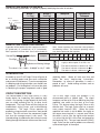
LOGIC PULSER KIT
MODEL LP-425K
Assembly and Instruction Manual
Elenco Electronics, Inc.
Copyright © 1995 Elenco Electronics, Inc.
REV-D Revised 2002
753262
PARTS LIST
If you are a student, and any parts are missing or damaged, please see instructor or bookstore.
If you purchased this kit from a distributor, catalog, etc., please contact Elenco Electronics (address/phone/email is at the back of this manual) for additional assistance, if needed.
RESISTORS
Qty.
2
1
2
3
1
4
1
2
1
Symbol
R1, R16
R17
R11, R13
R12, R14, R15
R8
R2, R7, R9, R10
R5
R3, R6
R4
Description
100W 5% 1/4W
470W 5% 1/4W
2kW 5% 1/4W
20kW 5% 1/4W
68kW 5% 1/4W
100kW 5% 1/4W
1MW 5% 1/4W
1.8MW 5% 1/4W
10MW 5% 1/4W
Qty.
2
1
1
1
Symbol
C6, C7
C4
C3
C1
Description
100pF (101) Discap
.001mF (102) Mylar
.01mF (103) Mylar
.1mF (104) Discap
Qty.
3
1
1
3
Symbol
D1,D4,D5
D3
D2
Q1,Q4,Q5
Description
Diode 1N4001
Diode 1N4148
Diode Zener 1N5246
Transistor 2N3904
Color Code
brown-black-brown-gold
yellow-violet-brown-gold
red-black-red-gold
red-black-orange-gold
blue-gray-orange-gold
brown-black-yellow-gold
brown-black-green-gold
brown-gray-green-gold
brown-black-blue-gold
Part #
131000
134700
142000
152000
156800
161000
171000
171800
181000
CAPACITORS
Qty.
1
1
1
Part #
221017
231017
241017
251010
Symbol
C5
C8
C2
Description
1mF Tantalum
10mF Lytic 35V
22mF Lytic 25V
Part #
260010
271016
272245
SEMICONDUCTORS
Qty.
2
1
Part #
314001
314148
315246
323904
1
Symbol
Q2, Q3
U1
Description
2N3906 Transistor
IC 4069 or 74C04
D6
LED
Part #
323906
334069
or 34C004
350001
MISCELLANEOUS
Qty.
1
1
1
1
2
1
3
1
Description
PC Board
Switch SPDT
Pulser Tip
Case
Screw #4 x 5/8”
IC Socket 14-pin
Pins
Alligator Clip Black
Qty.
1
1
1
1
3’
1”
1”
1
Part #
517009
541024
616001
623005
643450
664014
665001
680001
SPECIFICATIONS
Maximum Allowable Supply Voltage
Maximum Allowable Voltage on Output
Maximum Sync. Input Voltage
Operating Supply Voltage Range
Free Air Operating Temperature Range
Output Pulse Width at 100mA Load
Output Current
1) Pulser Mode
2) Square Wave Output
Pulse Repetition Rate
Sync. Input Impedance
+20V, +25V/15 sec.
+35V
+120V/15 sec.
4 - 15VDC
0 - 50OC
10mS
100mA Sink/Source
5mA Sink/Source
.5PPS / 400PPS
1MW
-1-
Description
Alligator Clip Red
Label Front
Label Back
Wire 22 Gauge Red 1.5”
Wire 2 Conductor
Tubing #20
Shrink Tubing (red)
Solder Tube
Part #
680002
724005
724006
814220
870500
890020
890312
9ST4
IDENTIFYING RESISTOR VALUES
Use the following information as a guide in properly identifying the value of resistors.
BAND 1
1st Digit
Bands
1 2 Multiplier
Tolerance
Color
Black
Brown
Red
Orange
Yellow
Green
Blue
Violet
Gray
White
Digit
0
1
2
3
4
5
6
7
8
9
Multiplier
BAND 2
2nd Digit
Color
Black
Brown
Red
Orange
Yellow
Green
Blue
Violet
Gray
White
Resistance
Tolerance
Color
Multiplier
Black
1
Brown
10
Red
100
Orange
1,000
Yellow
10,000
Green
100,000
Blue
1,000,000
Silver
0.01
Gold
0.1
Digit
0
1
2
3
4
5
6
7
8
9
Color
Silver
Gold
Brown
Red
Orange
Green
Blue
Violet
Tolerance
+10%
+5%
+1%
+2%
+3%
+.5%
+.25%
+.1%
IDENTIFYING CAPACITOR VALUES
Capacitors will be identified by their capacitance value in
pF (picofarads), nF (nanofarads), or mF (microfarads).
Most capacitors will have their actual value printed on
Second Digit
First Digit
Multiplier
103K
For the No.
0
1
2
3
Multiply By
1
10
100
1k
Tolerance*
Maximum Working Voltage
10mF 16V
100V
Multiplier
them. Some capacitors may have their value printed in
the following manner. The maximum operating voltage
may also be printed on the capacitor.
4
5
8
10k 100k .01
9
0.1
Note: The letter “R” may be used at times to
signify a decimal point; as in 3R3 = 3.3
* The letter M indicates a tolerance of +20%
The value is 10 x 1,000 = 10,000pF or .01mF 100V
The letter K indicates a tolerance of +10%
The letter J indicates a tolerance of +5%
INTRODUCTION
Assembly of your LP-425 Logic Pulser will prove to
be an exciting project and give much satisfaction
and personal achievement. If you have experience
in soldering and wiring technique, you should have
no problems. For the beginner, care must be given
in identifying the proper components and in good
soldering habits. Above all, take your time and
follow the easy step-by-step instructions.
Remember, “an ounce of prevention is worth a
pound of cure”. Avoid making mistakes and no
problems will occur.
CIRCUIT DESCRIPTION
The LP-425 Logic Pulser can produce a 10
microsecond pulse at 100mA load. The signal
frequency can be set to .5Hz or 400Hz by the pulse
repetition rate switch on the front of the Logic
Pulser. This feature makes the Logic Pulser a very
effective tool. The Logic Pulser also has a square
wave output terminal (SQ). When the pulse
repetition rate switch is set to 400Hz, the signal on
the square wave terminal is a square wave. When
the switch is set to .5Hz, the signal on the terminal
is a pulse, high for 90% of the time and ground for
the remaining 10%. The sync input terminal (SYNC)
Logic Pulser can be used to produce an externally
synchonized signal at the output.
The Elenco Model LP-425 Logic Pulser is a very
handy device for inspecting and repairing logic
circuits. By injecting a signal directly to the circuit,
you can avoid removing the ICs or other circuit
components. The Logic Pulser will thus help you to
troubleshoot wiring errors and malfunctioning
components. The Logic Pulser operates by
producing a large transient current for a short period
of time. This will not harm the components under
test since the average current is very small. The
injected voltage is produced by the transient current
flowing through the inherent resistance of the circuit.
-2-
CONSTRUCTION
Introduction
The most important factor in assembling your LP-425K Logic Pulser Kit is good soldering techniques. Using the
proper soldering iron is of prime importance. A small pencil type soldering iron of 25 - 40 watts is
recommended. The tip of the iron must be kept clean at all times and well tinned.
Safety Procedures
• Wear eye protection when soldering.
• Locate soldering iron in an area where you do not have to go around it or reach over it.
• Do not hold solder in your mouth. Solder contains lead and is a toxic substance. Wash your hands
thoroughly after handling solder.
• Be sure that there is adequate ventilation present.
Assemble Components
In all of the following assembly steps, the components must be installed on the top side of the PC board unless
otherwise indicated. The top legend shows where each component goes. The leads pass through the
corresponding holes in the board and are soldered on the foil side. Foil Side
Use only rosin core solder of 63/37 alloy.
DO NOT USE ACID CORE SOLDER!
Mount Part
What Good Soldering Looks Like
Bend Leads to
Hold Part
Solder and
Cut Off Leads
Types of Poor Soldering Connections
A good solder connection should be bright, shiny,
smooth, and uniformly flowed over all surfaces.
1.
Solder all components from
the copper foil side only.
Push the soldering iron tip
against both the lead and
the circuit board foil.
1. Insufficient heat - the
solder will not flow onto the
lead as shown.
Soldering Iron
Component Lead
Foil
Soldering iron positioned
incorrectly.
Circuit Board
2.
3.
4.
Apply a small amount of
solder to the iron tip. This
allows the heat to leave the
iron and onto the foil.
Immediately apply solder to
the opposite side of the
connection, away from the
iron.
Allow the heated
component and the circuit
foil to melt the solder.
Allow the solder to flow
around the connection.
Then, remove the solder
and the iron and let the
connection cool.
The
solder should have flowed
smoothly and not lump
around the wire lead.
Rosin
2. Insufficient solder - let the
solder flow over the
connection until it is
covered. Use just enough
solder
to
cover
the
connection.
Soldering Iron
Solder
Foil
Solder
Gap
Component Lead
Solder
3. Excessive solder - could
make connections that you
did not intend to between
adjacent foil areas or
terminals.
Soldering Iron
Solder
Foil
4. Solder bridges - occur
when solder runs between
circuit paths and creates a
short circuit. This is usually
caused by using too much
solder.
To correct this,
simply drag your soldering
iron across the solder
bridge as shown.
Here is what a good solder
connection looks like.
-3-
Soldering Iron
Foil
Drag
ASSEMBLE COMPONENTS TO THE PC BOARD
Refer to the top legend on the PC board, install and solder the following resistors. All are 1/4 watt, 5% tolerance.
(Resistors R11 and R12 install vertical).
R11 - 2kW Resistor
(red-black-red-gold)
(see Figure 1)
R12 - 20kW Resistor
(red-black-orange-gold)
(see Figure 1)
R14 - 20kW Resistor
(red-black-orange-gold)
R15 - 20kW Resistor
(red-black-orange-gold)
R9 - 100kW Resistor
(brown-black-yellow-gold)
R17 - 470W Resistor
(yellow-violet-brown-gold)
R7 - 100kW Resistor
(brown-black-yellow-gold)
R8 - 68kW Resistor
(blue-gray-orange-gold)
R10 - 100kW Resistor
(brown-black-yellow-gold)
R4 - 10MW Resistor
(brown-black-blue-gold)
R6 - 1.8MW Resistor
(brown-gray-green-gold)
R2 - 100kW Resistor
(brown-black-yellow-gold)
R13 - 2kW Resistor
(red-black-red-gold)
R5 - 1MW Resistor
(brown-black-green-gold)
R3 - 1.8MW Resistor
(brown-gray-green-gold)
R16 - 100W Resistor
(brown-black-brown-gold)
R1 - 100W Resistor
(brown-black-brown-gold)
Figure 1
Stand resistor on end.
-4-
ASSEMBLE COMPONENTS TO THE PC BOARD
Refer to the top legend on the PC board, install and solder the following diodes and capacitors.
D5 - 1N4001 Diode
(see Figure 2)
C8 - 10mF Lytic Capacitor
(see Figure 3A)
C6 - 100pF Discap
(may be marked 101)
D4 - 1N4001 Diode
(see Figure 2)
C7 - 100pF Discap
(may be marked 101)
D2 - 1N5246 Zener Diode
(see Figure 2)
D3 - 1N4148 Diode
(see Figure 2)
C2 - 22mF Lytic Capacitor
(see Figure 3A)
C5 - 1mF Tantalum
(May marked 105)
(see Figure 3B)
D1 - 1N4001 Diode
(see Figure 2)
C1 - .1mF Discap
(may be marked 104)
C3 - .01mF Mylar Capacitor
(May be marked 103)
C4 - .001mF Mylar Capacitor
(May be marked 102)
Figure 3A
Figure 2
When mounting diodes
horizontally, mount as
indicated by the band
(diodes have polarity).
Polarity Mark
(–)
Band
(+)
Figure 3B
(–)
(+)
Some capacitors have
polarity markings indicating
the positive (+) or negative
(–) lead. The PC board is
marked to show the lead
positions.
-5-
ASSEMBLE COMPONENTS TO THE PC BOARD
Refer to the top legend on the PC board, install and solder the following components.
Q3 - 2N3906 Transistor
(see Figure 7)
D6 - LED
(see Figure 8)
Q4 - 2N3904 Transistor
(see Figure 7)
Q1 - 2N3904 Transistor
(see Figure 7)
Q5 - 2N3904 Transistor
(see Figure 7)
U1 - 14-Pin IC Socket
U1 - 74C04 IC or 4069
(see Figure 5)
Q2 - 2N3906 Transistor
(see Figure 7)
SW1 - Switch
(see Figure 6)
P1, P2, P3 - Pins
Do not install the pins to the
PC board.
They will be
installed later. Tin (that is, put
a small amount of solder on)
the foil around the holes for
the three pins. Do not block
the hole. Tin the bottom fo
the pin as shown in Figure 4.
Figure 4
Tin Here
Figure 7
Figure 5
Install and solder the
socket. Insert the IC into
socket with the notch in
direction shown on the
legend.
Mount the transistor with the
flat side in the direction shown
on the top legend. Leave 1/4”
between the part and PC
board.
IC
the
the
top
1/4”
Notch
Figure 8
Cut a 3/8” piece of tubing for
each LED lead, to be used as
stand-offs. Mount the LED
with the flat side in the
direction shown on the top
legend.
Figure 6
Insert the tabs and terminals
into the PC board. Solder
terminals only.
Flat
Tubing
Tab
Tab
-6-
3/8”
Install the power cord as shown in Figure 9. Pull
the power cord wires apart about 2 inches on
one end. Strip the insulation off of both wires to
expose 1/4” of bare wire. Note that one wire is
ribbed on the edge. Solder the red alligator clip
to the ribbed wire. Solder the black clip to the
smooth wire. On the other side of the power
cord, pull the wires apart 1/2”. Strip 1/4” of
insulation off of both wires. Make a knot to serve
as a strain relief (about 1 inch from the end).
Solder the ribbed wire to the hole marked “+” and
the smooth wire to the hole marked “–”.
Place the unit into the case bottom and fasten
with two #4 screws. Do not over-tighten or the
holes may strip out.
Cut a 13/16” piece of red shrink tubing and slide
it over the pulser tip until it touches the plastic
case. Shrink the tubing by heating it with your
soldering iron. Be sure the soldering iron does
not contact the tubing or plastic case.
This completes the assembly procedure. Your Logic
Probe is now ready for testing.
Solder the wire to the clip, then bend
the tabs over the insulated wire.
Install the pulser tip as shown in Figure 10.
Using the 1 1/2” wire, strip 1/4” of insulation off of
both ends. Solder one end to point P on the PC
board. Solder the other end of the wire to the
pulser tip groove.
Clip
Punch out the five holes in the front label. Peel
the backing off the front and back labels and
stick them to the case as shown in Figure 11.
The front label should be placed toward the back
of the indent (toward the 3 pins) so that the LED
and switch holes align with the case holes.
Ribbed Wire
Insert the 3 pins P1, P2, and P3 into their holes in
the front label. Insert the PC board into the case
so that the LED and switch protrude through the
label (see Figure 11). Insert the 3 pins into the
PC board and solder (see Figure 4).
Smooth Wire
Figure 9
Front Label
Case (top)
Place knot
in case
Assembled
PC Board
Back Label
Case (bottom)
#4 x 5/8” Screws
Figure 10
Figure 11
-7-
Red Shrink
Tubing
TESTING YOUR LOGIC PULSER
Checking out your Logic Pulser for proper operation
is fairly easy. All that is needed is a 9V battery or
other DC power source (5-10V). Connect the red
alligator clip to the positive terminal of the battery
and the black clip to the negative terminal.
If you have an oscilloscope, connect it to the Square
(SQ) Pin and observe the waveforms shown in
Figure 12 for pulse repetition rate switch settings of
400PPS and .5PPS. The times shown are
approximate. If you do not get these waveforms:
Set the pulse repetition rate switch to the 0.5PPS
position. Check the red LED. It should blink once
every 2 seconds (0.5PPS). Set the switch to
400PPS. The Logic Pulser generates a frequency
of 400Hz. At this frequency, the LED flashes at a
rate that makes it appear to be on continuously. If
either of these tests fail:
a) Check the value and soldering of R16.
b) Check that transistor Q5 is the correct type and
is mounted with the flat as shown on the PC
board.
c) Check the value and soldering of capacitors C3,
C4 and C5.
Connect the pulser tip to the resistor combinations
shown in Figure 12 and observe the waveforms
shown for the pulser tip. If you do not get these
waveforms:
a) Check the input cable. The ribbed wire with the
red alligator clip should go to the hole marked
(+).
b) Check for cold solder joints and solder bridges
around the IC. Check that the IC notch matches
the notch shown on the PC board.
c) Check the soldering and polarity of diodes D1,
D2, D3 and D6 (LED).
d) Check that transistor Q5 is the correct type and
is mounted with the flat side as shown on the PC
board.
e) Check the soldering and the values of capacitors
C1 through C5.
f) Check the soldering and the values of resistors
R1 through R5 and R15 through R17.
a) Check that transistors Q1 through Q4 are the
correct type and are mounted with the flat side
as shown on the PC board.
b) Check the soldering and polarity of diodes D4
and D5.
c) Check the soldering and values of resistors R7
through R14.
d) Check the soldering and values of capacitors C3
through C8.
Figure 12
-8-
SCHEMATIC DIAGRAM
Note: All resistors are 5% 1/4W
IC 74C04 or 4069
Schematic Diagram
LP-425
-9-
QUIZ
1) The LP-425 Logic Pulser can produce a _______
microsecond pulse at 100mA.
A. 30
B. 15
C. 10
D. 20
6) The LP-425 Logic Pulser is a very handy device for
inspecting and repairing __________________.
A. motor circuits.
B. logic circuits.
C. lighting circuits.
D. radar circuits.
2) The Logic Pulser operates by producing a large
transient current for a __________ period of time.
A. long
B. short
C. long and short
D. none of the above.
7) The Sync input impedance of the LP-425 is
___________.
A. 3MW.
B. 2MW.
C. 4MW.
D. 1MW.
3) The signal frequency of the Logic Pulser are _____ Hz
and _____ Hz.
A. 10, 100
B. 0.1, 300
C. 0.5, 400
D. none of the above.
8) When the switch is set to 0.5Hz, the signal on the
terminal is a pulse, high for ________ of the time and
ground for the remaining _________.
A. 50%, 50%.
B. 20%, 80%.
C. 90%, 10%.
D. 60%, 40%.
4) The Logic Pulser also has a ___________ wave
output terminal.
A. square
B. sine
C. saw
D. cosine
9) The Sync Input Terminal (SYNC) Logic Pulser can be
used to produce an externally synchronized signal at
the ____________.
A. output.
B. input.
C. input and output.
D. none of the above.
5) In operating supply voltage range is ____________.
A. 0V to 10VDC.
B. 4V to 15VDC.
C. 20V to 45VDC.
D. 0.1V to 5VDC.
10) The Free air operating temperature range is ______.
A. 0 - 100OC.
B. 30 - 40OC.
C. 0 - 50OC.
D. 25 - 75OC.
Other Logic Probe Kits Available
Logic Probe Model LP-525K (kit)
Logic Probe Model LP-535K (kit)
Digital Logic Probe in kit form provides convenient and
precise use in measurement of logic circuits. It displays
logic levels (high or low), pulses and voltage transients
down to 30 nanoseconds and a maximum input of 20MHz.
Large PC board and detailed manual for fast construction.
Advanced design with audible sound for signal detection
in logic circuits. It displays logic levels (high or low) pulses
and voltage transients down to 10 nanoseconds. High
intensity LED readouts provide instant response to the
logic state. Simplified circuitry for fast construction.
Detailed instructions, illustrations and testing included.
Answers to Quiz: 1. C; 2. B; 3. C; 4. A; 5. B; 6. B; 7. D; 8. C; 9. A; 10. C
-10-
Elenco Electronics, Inc.
150 W. Carpenter Avenue
Wheeling, IL 60090
(847) 541-3800
http://www.elenco.com
e-mail: [email protected]