1
AMBE-3000F™ Vocoder Chip
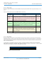
Users Manual
Version 3.4
April, 2014
DVSI Confidential Proprietary
AMBE-3000F™ Vocoder Chip Users Manual
Version 3.4, April, 2014
AMBE-3000F™ Vocoder Chip
Users Manual
Version 3.4
April, 2014
(The most up to date version of the manual is always available at www.dvsinc.com)
Copyright, 2008
Digital Voice Systems, Inc.
234 Littleton Road
Westford, MA 01886
This document may not, in whole or in part be copied, photocopied, reproduced, translated, or reduced to any electronic
medium or machine readable form without prior consent in writing from Digital Voice Systems, Incorporated.
Every effort has been made to ensure the accuracy of this manual. However, Digital Voice Systems, Inc. makes no warranties
with respect to the documentation and disclaims any implied warranties of merchantability and fitness for a particular purpose.
Digital Voice Systems, Inc. shall not be liable for any errors or for incidental or consequential damages in connection with the
furnishing, performance, or use of this manual or the examples herein. This includes business interruption and/or other loss
which may arise from the use of this product. The information in this document is subject to change without notice.
Trademarks
AMBE-3000F™ Vocoder Chip is a registered trademark of Digital Voice Systems, Inc. Other product names mentioned may
be trademarks or registered trademarks of their respective companies and are the sole property of their respective
manufacturers.
All Rights Reserved.
Data subject to change.
Page ii
(Subject to Change)
DVSI CONFIDENTIAL PROPRIETARY
AMBE-3000F™ Vocoder Chip Users Manual
Version 3.4, April, 2014
AMBE-3000F™ Vocoder Chip END USER License Agreement
1. Preliminary Statements and Definitions
Information from disclosure by such third party. Third parties shall agree to accept all
the terms and conditions under either Agreement or the END USER Agreement.
1.1 This nonexclusive end user product license agreement is a legal agreement between
the customer (the END USER) and Digital Voice Systems, Inc. (DVSI) covering the
terms and conditions under which DVSI's proprietary content (that may consist of and
is not limited to software, hardware, documentation and other material) is licensed to
the END USER as part of this PRODUCT.
a) The PRODUCT shall mean the Hardware, Software, Documentation and other
materials that were provided by DVSI, either directly or indirectly through distributors
or agents, to END USER as part of a sale, delivery or other transaction.
b) Hardware can be in the form of Integrated Circuits (such as Digital signal Processors)
Circuit boards and electronics enclosed in a chassis. DVSI’s AMBE-3000F™ Vocoder
Chip is an example of an Integrated Circuit.
c) Software can be in form of computer code, firmware masked into an IC or stored or
embedded into ROM or RAM or Flash memory, or software stored on any media (such
as CD-ROM, floppy disk, hard drive, solid-state memory or the Internet)
d) Documentation means written or electronic information, including user manuals,
technical documents, training materials, specifications or diagrams, that pertain to or
are delivered with the PRODUCT in any manner (including in print, on CD-ROM, or
on-line).
1.2 DVSI has developed a number of voice coding methods and algorithms (the
“Technology”) which include DVSI’s Advanced Multi-Band Excitation (“AMBE”) ,
AMBE+™, and AMBE+2™ voice coders. The Technology codes speech at low bit
rates and may include error correction, echo cancellation and other auxiliary functions.
1.3 "DVSI Voice Compression Software" shall mean the voice coding Software that
implements or embodies the Technology and is embedded into or otherwise provided
with the PRODUCT.
4. Term and Termination
4.1 This Agreement is effective upon initial delivery of the PRODUCT and shall remain in
effect until terminated in accordance with this agreement.
4.2 This Agreement shall terminate automatically without notice from DVSI if END USER
fails to comply with any of the material terms and conditions herein. END USER may
terminate this Agreement at any time upon written notice to DVSI certifying that END
USER has complied with the provisions of Section 3.
4.3 Upon termination of this Agreement for any reason, END USER shall: (i) return the
PRODUCT and documentation purchased or acquired, or in Licensee’s possession, to
DVSI; (ii) have no further rights to any DVSI Software or the Technology without a
separate written license from DVSI; (iii) discontinue all use of the PRODUCT;
All confidentiality obligations of Customer and all limitations of liability and disclaimers
and restrictions of warranty shall survive termination of this Agreement. In addition, the
provisions of the sections titled "U.S. Government End User Purchasers" and "General
Terms Applicable to the Limited Warranty Statement and End User License" shall
survive termination of this Agreement.
5. Payments
5.1 In consideration of the materials delivered as part of the Product, and in consideration
of the license granted by DVSI for the PRODUCT, and in consideration of DVSI's
performance of its obligations hereunder, the END USER agrees to pay to DVSI the
fees as specified in DVSI's invoice. Payments of fees shall be received by DVSI prior
to shipment of the PRODUCT.
6. Proprietary Notices
1.4 "DVSI Voice Codec" shall mean the DVSI Voice Compression Software, any
PRODUCT Hardware into which the DVSI Voice Compression Software is embedded
or executed and any associated Documentation.
1.5 DVSI represents that it owns certain “Proprietary Rights” in the PRODUCT including
patent rights, copyrights, trademarks and trade secrets. These rights include one or
more of the following US Patents #5,630,011; #5,649,050; #5,701,390; #5,715,365;
#5,754,974; #5,826,222; #5,870,405; #6,161,089; #6,199,037; #6,912,495;
#7,634,399; #7,957,963; #7,970,606; #8,036,886; #8,200,497; #8,315,860 and
#8,359,197; and under other US and foreign patents and patents pending. AMBE,
AMBE+™ and AMBE+2™ are trademarks of Digital Voice Systems, Inc.
6.1 END USER shall maintain and not remove any copyright or proprietary notice on or in
the PRODUCT.
6.2 Reproduction of non-proprietary information found in DVSI Users Manuals or data
sheets is permissible only if the END USER reproduces without alteration, and
includes all copyright and other proprietary notices, all associated warranties,
conditions and limitations on all copies, in any form.
7. Proprietary Information
7.1 The parties agree that the PRODUCT shall be considered Proprietary Information.
1.6 “END USER” shall mean the person and/or organization to whom the DVSI Vocoder
Product (software or hardware) was delivered or provided to as specified in the
purchase order or other documentation. In the event that the END USER transfers his
rights under this license to a third party as specified in Section 3.0, then this third party
shall become an “END USER”.
7.2 Except as otherwise provided in this Agreement, END USER shall not use, disclose,
make, or have made any copies of the Proprietary Information, in whole or in part,
without the prior written consent of DVSI.
8. Limited Warranty
1.7 DVSI reserves the right to make modifications and other changes to its products and
services at any time and to discontinue any product or service without notice.
2. License Granted
2.1 Subject to the conditions herein and upon initial use of the DVSI Product, DVSI hereby
grants to END USER a non-exclusive, limited license to use the DVSI Voice
Compression Software and Technology within the PRODUCT. No license is granted
for any use of the DVSI Voice Compression Software or Technology on any other
device or Hardware or in any manner other than within the original unmodified
PRODUCT purchased from DVSI. No license is granted to copy or modify the DVSI
Voice Compression Software or the PRODUCT either in whole or in part.
2.2 No license, right or interest in any trademark, trade name or service mark of DVSI is
granted under this Agreement. END USER acknowledges that the PRODUCT may
contain trade secrets of DVSI, including but not limited to the specific design, and
associated interface information.
2.3 END USER shall not copy, extract, reverse engineer, disassemble, de-compile or
otherwise reduce the DVSI Voice Compression Software to human-readable form.
END USER shall not alter, duplicate, make copies of, create derivative works from,
distribute, disclose, provide or otherwise make available to others, the DVSI Voice
Compression Software and Technology and/or trade secrets contained within the
PRODUCT in any form to any third party without the prior written consent of DVSI. The
END USER shall implement reasonable security measures to protect such trade
secrets.
2.4 This is a license, not a transfer of title, to the DVSI Voice Compression Software,
Technology and Documentation, and DVSI retains ownership and title to all copies.
3. Transfer of License
3.1 The END USER shall have the right to transfer the rights under this Agreement to a
third party by either (i) providing the third party with a copy of this Agreement or (ii)
providing the third party with an agreement written by the END USER ( hereinafter
“END USER Agreement”) so long as the END USER Agreement is approved in writing
by DVSI prior to transfer of the PRODUCT. The END USER Agreement shall contain
comparable provisions to those contained herein for protecting the Proprietary
8.1 DVSI warrants the PRODUCT to be free from defects in materials and workmanship
under normal use for a period of ninety (90) days from the date of delivery. The date of
delivery is set forth on the packaging material in which the Product is shipped. This
limited warranty extends only to the Customer who is the original purchaser. If the
PRODUCT is found to be defective and the condition is reported to DVSI, within the
warranty period, DVSI may, at its option, repair, replace, or refund of the purchase
price of the PRODUCT. DVSI may require return of the PRODUCT as a condition to
the remedy.
Restrictions. This warranty does not apply if the Product (a) has been altered, (b) has
not been installed, operated, repaired, or maintained in accordance with instructions
supplied by DVSI, (c) has been subjected to abnormal physical or electrical stress,
misuse, negligence, or accident;
8.2 Except as stated in Section 8.1, the PRODUCT is provided "as is" without warranty of
any kind. DVSI does not warrant, guarantee or make any representations regarding
the use, or the results of the use, of the PRODUCT with respect to its correctness,
accuracy, reliability, speech quality or otherwise. The entire risk as to the results and
performance of the PRODUCT is assumed by the END USER. After expiration of the
warranty period, END USER, and not DVSI or its employees, assumes the entire cost
of any servicing, repair, replacement, or correction of the PRODUCT.
8.3 DVSI represents that, to the best of its knowledge, it has the right to enter into this
Agreement and to grant a license to use the PRODUCT to END USER.
8.4 Except as specifically set forth in this Section 8, DVSI makes no express or implied
warranties including, without limitation, the warranties of merchantability or fitness for a
particular purpose or arising from a course of dealing, usage or trade practice, with
respect to the PRODUCT. Some states do not allow the exclusion of implied
warranties, so the above exclusion may not apply to END USER. No oral or written
information or advice given by DVSI or its employees shall create a warranty or in any
way increase the scope of this warranty and END USER may not rely on any such
information or advice. The limited warranties under this Section 8 give END USER
specific legal rights, and END USER may have other rights which vary from state to
state.
9. Limitation of Liability
Page iii
(Subject to Change)
DVSI CONFIDENTIAL PROPRIETARY
The END USER agrees that the limitations of liability and disclaimers set forth herein
will apply regardless of whether the END USER has accepted the product or service
delivered by DVSI.
9.1 In no event shall DVSI be liable for any special, incidental, indirect or consequential
damages resulting from the use or performance of the PRODUCT whether based on
an action in contract, or for applications assistance, or product support, or tort
(including negligence) or otherwise (including, without limitation, damages for loss of
business revenue, profits, business interruption, and loss of business information or
lost or damaged data), even if DVSI or any DVSI representative has been advised of
the possibility of such damages.
9.2 Because some states or jurisdictions do not allow the exclusion or limitation of liability
for consequential or incidental damages, the above limitations may not apply to END
USER.
9.3 DVSI's maximum liability for damages arising under this Agreement shall be limited to
20% (twenty percent) of the fees paid by END USER for the particular PRODUCT that
gave rise to the claim or that is the subject matter of, or is directly related to, the cause
of action.
10. Taxes
10.1 All payments required under Section 4 or otherwise under this Agreement are
exclusive of taxes and END USER agrees to bear and be responsible for the payment
of all such taxes (except for taxes based upon DVSI's income) including, but not
limited to, all sales, use, rental receipt, personal property or other taxes which may be
levied or assessed in connection with this Agreement.
11. Export
11.1 United States export laws and regulations prohibit the exportation of certain products
or technical data received from DVSI under this Agreement to certain countries except
under a special validated license. Some of the restricted countries include: Libya,
Cuba, North Korea, Iraq, Serbia, Taliban in Afghanistan, Sudan, Burma, and Iran. The
END USER hereby gives its assurance to DVSI that it will not knowingly, unless prior
authorization is obtained from the appropriate U.S. export authority, export or reexport, directly or indirectly to any of the restricted countries any products or technical
data received from DVSI under this Agreement in violation of said United States
Export Laws and Regulations. DVSI neither represents that a license is not required
nor that, if required, it will be issued by the U.S. Department of Commerce. Licensee
shall assume complete and sole responsibility for obtaining any licenses required for
export purposes.
12. Governing Law
12.1 This Agreement is made under and shall be governed by and construed in
accordance with the laws of the Commonwealth of Massachusetts, (USA), except that
body of law governing conflicts of law. If any provision of this Agreement shall be held
unenforceable by a court of competent jurisdiction, that provision shall be enforced to
the maximum extent permissible, and the remaining provisions of this Agreement shall
remain in full force and effect. This Agreement has been written in the English
language, and the parties agree that the English version will govern.
Page iv
(Subject to Change)
DVSI CONFIDENTIAL PROPRIETARY
Table of Contents
1
2
3
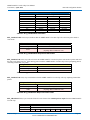
PRODUCT INTRODUCTION ..............................................................................................1
1.1
Advances in Vocoder Design ....................................................................................................................1
1.2
AMBE-3000™ Vocoder Chip Features .....................................................................................................1
1.3
Typical Applications...................................................................................................................................2
HARDWARE INFORMATION .............................................................................................3
2.1
Special Handling and Moisture Sensitivity ................................................................................................3
2.2
Package Details.........................................................................................................................................4
2.2.1 128-pin Low-Profile Quad Flat Pack (LQFP).................................................................................................. 4
2.2.2 179 Pin Ball Grid Array (BGA) ........................................................................................................................ 5
2.3
Pin Assignment Layouts ............................................................................................................................6
2.3.1 LQFP Package.................................................................................................................................................. 6
2.3.2 BGA Package Pins (Bottom View).................................................................................................................... 7
2.4
AMBE-3000F™ Vocoder Chip Markings...................................................................................................8
2.4.1 AMBE-3000F™ Vocoder Chip LQFP Markings.............................................................................................. 8
2.4.2 AMBE-3000F™ Vocoder Chip BGA Markings ................................................................................................ 9
2.5
Pin Out Table...........................................................................................................................................10
2.6
Hardware Configuration Pins...................................................................................................................18
2.7
Crystal / Oscillator Usage ........................................................................................................................19
2.7.1 External Clock Source .................................................................................................................................... 19
2.7.2 Crystal Oscillator............................................................................................................................................ 19
2.7.3 Input Clock Requirements............................................................................................................................... 20
ELECTRICAL CHARACTERISTICS AND REQUIREMENTS ..........................................21
3.1
Normal Operating Conditions ..................................................................................................................21
3.2
Recommended Operating Conditions .....................................................................................................21
3.3
Absolute Maximum Ratings.....................................................................................................................21
3.4
Thermal Resistance Characteristics........................................................................................................22
3.5
Power Sequencing Requirements...........................................................................................................22
3.6
Reset Behavior ........................................................................................................................................23
3.6.1 Reset to Ready Packet Timing......................................................................................................................... 23
3.6.2 Behavior of RTSn and TX_RDY following a RESET....................................................................................... 23
3.7
Signal Transition Levels ..........................................................................................................................24
3.8
Power-Down Sequencing: .......................................................................................................................25
3.9
Low Power Modes ...................................................................................................................................25
3.9.1 Run State ......................................................................................................................................................... 26
3.9.2 Idle State ......................................................................................................................................................... 26
3.9.3 Standby State................................................................................................................................................... 26
3.9.4 Halt State ........................................................................................................................................................ 26
3.9.5 Power Modes .................................................................................................................................................. 27
3.9.6 Low power mode when using the UART Packet Interface .............................................................................. 27
3.9.7 Low Power Mode when using the McBSP Packet Interface ........................................................................... 27
Page v
(Subject to Change)
DVSI CONFIDENTIAL PROPRIETARY
AMBE-3000F™ Vocoder Chip Users Manual
Version 3.4, April, 2014
3.9.8 Low Power Mode when using the McBSP Codec Interface ............................................................................ 27
3.9.9 Low Power Mode when using the SPI Codec Interface .................................................................................. 28
3.9.10 Low Power Mode when using the Parallel Packet Interface ......................................................................... 28
3.9.11 Additional Requirements when Low Power Mode is enabled........................................................................ 28
3.9.12 Typical AMBE-3000F™ Vocoder Chip Power Measurements: .................................................................... 28
4
5
INITIAL DESIGN CONSIDERATIONS ..............................................................................30
4.1
Vocoder Speech and FEC Rate Selection ..............................................................................................30
4.2
Interface Selection...................................................................................................................................30
4.3
A/D – D/A Codec chip Selection..............................................................................................................31
4.4
Vocoder State..........................................................................................................................................31
4.5
Special Functions Description .................................................................................................................32
4.5.1 Voice Activity Detection & Comfort Noise Insertion ...................................................................................... 32
4.5.2 Echo Canceller (EC_ENABLE TQFP pin120 BGA pin D5)........................................................................... 32
4.5.3 DTMF Dual Tone Multiple Frequency, Detection and Generation................................................................ 33
4.5.4 Soft Decision Error Correction....................................................................................................................... 33
4.5.5 Skew Control (SK_ENABLE TQFP pin 6 BGA pin D3) ................................................................................. 34
4.5.6 Noise Suppressor (NS_ENABLE TQFP pin 7 BGA pin D2) ........................................................................... 34
4.5.7 Companding Using A-Law and µ-Law ........................................................................................................... 34
I/O MANAGEMENT...........................................................................................................35
5.1
Operating Modes Introduction .................................................................................................................38
5.2
Codec mode ............................................................................................................................................39
5.2.1 Timing of channel transmit packets in Codec Mode ....................................................................................... 40
5.2.2 Timing of channel receive packets in Codec Mode......................................................................................... 41
5.2.3 I/O Handler in Codec Mode............................................................................................................................ 42
5.3
Packet Mode............................................................................................................................................43
5.3.1 I/O Handler In Packet Mode........................................................................................................................... 44
5.4
Switching between codec mode and packet mode using packets ..........................................................45
5.5
SPI Interface ............................................................................................................................................46
5.6
UART Interface........................................................................................................................................47
5.6.1 UART_TX Pin State ........................................................................................................................................ 48
5.7
McBSP Interface......................................................................................................................................48
5.7.1 McBSP Selected for Codec Interface .............................................................................................................. 48
5.7.2 McBSP Selected for Packet Interface ............................................................................................................. 49
5.8
Parallel Interface......................................................................................................................................51
5.8.1 Parallel Port Packet Interface ........................................................................................................................ 51
5.9
Codec A/D / D/A Interface .......................................................................................................................53
5.10 Vocoder Front End Requirements...........................................................................................................53
5.11 Interfacing a codec to the AMBE-3000F™ Vocoder chip........................................................................55
5.11.1 The Texas Instruments General purpose TLV320AIC14 ............................................................................... 55
5.11.2 The Texas Instruments PCM3500 General purpose codec............................................................................ 56
6
DATA AND CONFIGURATION PACKETS.......................................................................58
6.1
Overview..................................................................................................................................................58
6.2
Codec Mode Operation ...........................................................................................................................58
Page vi
(Subject to Change)
DVSI CONFIDENTIAL PROPRIETARY
AMBE-3000F™ Vocoder Chip Users Manual
Version 3.4, April, 2014
6.3
Packet Mode Operation...........................................................................................................................58
6.4
Packet Interfaces.....................................................................................................................................59
6.5
Packet Format .........................................................................................................................................59
6.5.1 START_BYTE (1 byte)..................................................................................................................................... 59
6.5.2 LENGTH (2 bytes) .......................................................................................................................................... 59
6.5.3 TYPE (1 byte).................................................................................................................................................. 60
6.5.4 Packet Fields................................................................................................................................................... 60
6.5.5 Parity Field (Parity is enabled by default)...................................................................................................... 61
6.6
Control Packet Format (Packet Type 0x00) ............................................................................................61
6.6.1 Control Packet Fields and Response Fields ................................................................................................... 61
6.7
Input Speech Packet Format (Packet Type 0x02) ..................................................................................79
6.7.1 Speech Packet Fields ...................................................................................................................................... 79
6.8
Output Speech Packets Format (Packet Type 0x02)..............................................................................82
6.9
Input Channel Packet Format (Packet Type 0x01) .................................................................................82
6.9.1 Channel Packet Fields .................................................................................................................................... 82
6.10 Output Channel Packet Format (Packet Type 0x01) ..............................................................................84
6.11 Example Packets.....................................................................................................................................84
6.11.1 Speech Packet Example 1 .............................................................................................................................. 84
6.11.2 Speech Packet Example 2 .............................................................................................................................. 85
6.11.3 Channel Packet Example 1 ............................................................................................................................ 86
6.11.4 Channel Packet Example 2 ............................................................................................................................ 87
7
8
APPENDICES ...................................................................................................................88
7.1
Algorithmic and Processing Delays.........................................................................................................88
7.2
Vocoder Rate by Index Number ..............................................................................................................89
7.3
Rate - Control Words / Configuration Pin Settings ..................................................................................91
SUPPORT .........................................................................................................................93
8.1
DVSI Contact Information........................................................................................................................93
9
ENVIRONMENTAL SPECIFICATIONS ............................................................................94
10
IC CHIP SOFTWARE ERRATA ........................................................................................97
11
HISTORY OF REVISIONS ................................................................................................99
List of Figures
Figure 1 TQFP Mechanical Details .......................................................................................... 4
Figure 2 BGA Mechanical Details................................................................................................ 5
Figure 3 AMBE-3000F™ Vocoder Chip Pins for LQFP Package ..................................................... 6
Figure 4 AMBE-3000F™ Vocoder Chip Pins Bottom View of BGA chip .......................................... 7
Figure 5 AMBE-3000F™ Vocoder Chip LQFP Markings ............................................................... 8
Figure 6 AMBE-3000F™ Vocoder Chip Markings for BGA ........................................................... 9
Figure 7 X1/XCLKIN and X2 with TTL/CMOS Clock Source ....................................................... 19
Figure 8 X1/XCLKIN and X2 with Crystal Oscillator................................................................. 20
Figure 9 Input Clock Requirements ...................................................................................... 20
Page vii
(Subject to Change)
DVSI CONFIDENTIAL PROPRIETARY
AMBE-3000F™ Vocoder Chip Users Manual
Version 3.4, April, 2014
Figure
Figure
Figure
Figure
Figure
Figure
Figure
Figure
Figure
Figure
Figure
Figure
Figure
Figure
Figure
Figure
Figure
Figure
Figure
Figure
Figure
Figure
Figure
Figure
Figure
Figure
Figure
Figure
Figure
Figure
Figure
10
11
12
13
14
15
16
17
18
19
20
21
22
23
24
25
26
27
28
29
30
31
32
33
34
35
36
37
38
39
40
Cascading Resets ................................................................................................ 23
TX_RDY after Reset............................................................................................. 24
Output Levels ..................................................................................................... 24
Input Levels ....................................................................................................... 25
AMBE-3000F™ Vocoder Chip Power States.............................................................. 25
Power Mode States Basic Timing ........................................................................... 26
Power Modes...................................................................................................... 27
Basic Operation .................................................................................................. 30
Typical Echo Path................................................................................................ 33
Switching between Packet and Codec Modes ........................................................... 38
Codec Mode (SPI Interface).................................................................................. 39
Codec Mode (McBSP Interface) ............................................................................. 40
TX_RDY with Skew Control Off .............................................................................. 40
TX_RDY with Skew Control On .............................................................................. 41
TX_RDY Timing................................................................................................... 41
TX_RDY Frame Interval ....................................................................................... 41
TX_RDY Frame interval Examples.......................................................................... 42
Interface BLOCK Diagram Codec Mode ................................................................... 43
Interface Block Diagram Packet Mode .................................................................... 44
Packet Mode....................................................................................................... 45
SPI Timing ......................................................................................................... 46
Timing of SPI_GENSTE ........................................................................................ 47
Timing of McBSP When Selected as Codec Interface................................................. 49
Timing of McBSP when Selected as Packet Interface................................................. 50
PPT Interface Timing ........................................................................................... 52
Typical Vocoder Implementation ........................................................................... 53
Vocoder Front End .............................................................................................. 54
Front End Input Filter Mask .................................................................................. 54
Front End Output Filter Mask ................................................................................ 55
AMBE-3000F™ Vocoder Chip and TLV320AIC14 Interface Block Diagram..................... 56
AMBE-3000F™ Vocoder Chip and PCM3500 Interface Block Diagram .......................... 57
List of Tables
Table
Table
Table
Table
Table
Table
Table
Table
Table
Table
Table
Table
Table
Table
Table
Table
Table
Table
Table
1 Pinout List ............................................................................................................ 16
2 Hardware Configuration Settings .............................................................................. 18
3 Normal Operating Conditions ................................................................................... 21
4 Recommended Operating Conditions......................................................................... 21
5 Absolute Maximum Ratings ..................................................................................... 22
6 Thermal Resistance Characteristics........................................................................... 22
7 Voltage Supply Pins................................................................................................ 22
8 Typical AMBE-3000F™ Vocoder Chip Power Measurements........................................... 28
9 Physical Interface Selection ..................................................................................... 31
10 Soft Decision Error Correction ................................................................................ 33
11 Companding Control ............................................................................................. 34
12 Companding Selection .......................................................................................... 34
13 ECMODE_IN Flags ................................................................................................ 36
14 ECMODE_OUT FLAGS............................................................................................ 36
15 DCMODE_IN Flags................................................................................................ 37
16 DCMODE_OUT Flags ............................................................................................. 37
17 SPI Interface Pins ................................................................................................ 46
18 SPI Timing .......................................................................................................... 47
19 UART Interface Pins.............................................................................................. 47
Page viii
(Subject to Change)
DVSI CONFIDENTIAL PROPRIETARY
AMBE-3000F™ Vocoder Chip Users Manual
Version 3.4, April, 2014
Table
Table
Table
Table
Table
Table
Table
Table
Table
Table
Table
Table
Table
Table
Table
Table
Table
Table
Table
Table
Table
Table
Table
Table
Table
Table
Table
Table
Table
Table
Table
Table
Table
Table
Table
Table
Table
Table
Table
Table
Table
Table
Table
Table
Table
Table
Table
Table
Table
Table
Table
Table
Table
20
21
22
23
24
25
26
27
28
29
30
31
32
33
34
35
36
37
38
39
40
41
42
43
44
45
46
47
48
49
50
51
52
53
54
55
56
57
58
59
60
61
62
63
64
65
66
67
68
69
70
71
72
UART Baud Rates ................................................................................................. 48
McBSP Interface Pins ............................................................................................ 48
McBSP Codec Interface Timing ............................................................................... 49
McBSP Packet Interface Timing .............................................................................. 50
McBSP Clock Rates ............................................................................................... 51
Parallel (PPT) Interface Pins................................................................................... 51
PPT Timing.......................................................................................................... 52
Control Register Value for the TLV320AIC14 ............................................................ 56
General Packet Format WITHOUT Parity Field ........................................................... 59
General Packet Format WITH Parity Field ................................................................. 59
Packet Types ....................................................................................................... 60
General Field Format ............................................................................................ 60
Control Packet Fields ............................................................................................ 62
PKT_CHANNEL(0) Field Format............................................................................... 62
PKT_CHANNEL(0) Response Field Format ................................................................ 62
PKT_ECMODE Field Format .................................................................................... 62
PKT_ECMODE Field Response Format ...................................................................... 63
PKT_DCMODE Field Format.................................................................................... 63
PKT_DCMODE Response Field Format...................................................................... 63
PKT_COMPAND Field Format .................................................................................. 63
PKT_COMPAND Field Options ................................................................................. 63
PKT_COMPAND Response Field Format .................................................................... 64
PKT_RATET Field Format ....................................................................................... 64
PKT_RATET Response Field Format ......................................................................... 64
PKT_RATEP Field Format ....................................................................................... 64
PKT_RATEP Field Example ..................................................................................... 65
PKT_RATEP Response Field Format ......................................................................... 65
PKT_INIT Field Format .......................................................................................... 65
PKT_INIT Field - Data ........................................................................................... 66
PKT_INIT Response Field Format ............................................................................ 66
PKT_LOWPOWER Field Format ............................................................................... 66
PKT_LOWPOWER Field Settings .............................................................................. 66
PKT_LOWPOWER Response Field Format ................................................................. 67
PKT_CODECCFG Field Format ................................................................................ 67
PKT_CODECCFG Field Example Data (default values shown)....................................... 67
PKT_CODECCFG Response Field Format .................................................................. 67
PKT_CODECSTART Field Format ............................................................................. 67
PKT_CODECSTART Field Data ................................................................................ 68
PKT_CODECSTART Response Field Format ............................................................... 68
PKT_CODECSTOP Field ......................................................................................... 68
PKT_CODECSTOP Response Field Format................................................................. 68
PKT_CHANFMT Field ............................................................................................. 69
PKT_CHANFMT Data Settings ................................................................................. 69
PKT_CHANFMT Response Field ............................................................................... 69
PKT_SPCHFMT Field.............................................................................................. 70
PKT_SPCHFMT Data Settings ................................................................................. 70
PKT_SPCHFMT Response Field................................................................................ 70
PKT_PRODID Field................................................................................................ 71
PKT_PRODID Response Field.................................................................................. 71
PKT_VERSTRING Field .......................................................................................... 71
PKT_VERSTRING Response Field ............................................................................ 72
PKT_READY Field ................................................................................................. 72
PKT_HALT Field.................................................................................................... 72
Page ix
(Subject to Change)
DVSI CONFIDENTIAL PROPRIETARY
AMBE-3000F™ Vocoder Chip Users Manual
Version 3.4, April, 2014
Table
Table
Table
Table
Table
Table
Table
Table
Table
Table
Table
Table
Table
Table
Table
Table
Table
Table
Table
Table
Table
Table
Table
Table
Table
Table
Table
Table
Table
Table
Table
Table
Table
Table
Table
Table
Table
Table
Table
Table
Table
Table
Table
Table
73 PKT_RESET Field.................................................................................................. 72
74 Software Override of Hardware Configuration Pins .................................................... 73
75 PKT_RESETSOFTCFG Field ..................................................................................... 73
76 PKT_GETCFG Field................................................................................................ 74
77 PKT_GETCFG Response Field ................................................................................. 74
78 PKT_READCFG Field ............................................................................................. 74
79 PKT_READCFG Response Field ............................................................................... 74
80 PKT_PARITYMODE Field Format.............................................................................. 74
81 PKT_PARITYMODE Response Field .......................................................................... 75
82 PKT_ WRITEI2C Field Format ................................................................................. 75
83 PKT_WRITEI2C Response Field............................................................................... 75
84 PKT_CLRCODECRESET Field Format ........................................................................ 75
85 PKT_CLRCODECRESET Response Field..................................................................... 76
86 PKT_SETCODECRESET Field Format ........................................................................ 76
87 PKT_SETCODECRESET Response Field..................................................................... 76
88 PKT_DISCARDCODEC Field Format ......................................................................... 76
89 PKT_DISCARDCODEC Response Field ...................................................................... 76
90 PKT_DELAYNUS Field Format ................................................................................. 77
91 PKT_DELAYNUS Response Field.............................................................................. 77
92 PKT_DELAYNUS Field Format ................................................................................. 77
93 PKT_DELAYNNS Response Field.............................................................................. 77
94 PKT_RTSTHRESH Field Format ............................................................................... 77
95 PKT_RTSTHRESH Response Field ............................................................................ 78
96 PKT_GAIN Field Format......................................................................................... 78
97 PKT_GAIN Response Field ..................................................................................... 78
98 Speech Packet Fields ............................................................................................ 79
99 SPEECHD Field Format .......................................................................................... 79
100 CMODE Field Format ........................................................................................... 80
101 CMODE Parameters Table .................................................................................... 80
102 CMODE Parameters Table Key .............................................................................. 80
103 TONE Field Format.............................................................................................. 80
104 TONE Index Values ............................................................................................. 81
105 TONE AMPLITUDE Values..................................................................................... 81
106 Channel Packet Fields ......................................................................................... 82
107 CHAND Field - Format ......................................................................................... 82
108 CHAND4 Field - Format ....................................................................................... 83
109 SAMPLES Field - Format ...................................................................................... 83
110 TONE Field Format.............................................................................................. 84
111 Speech Packet Example 1 .................................................................................... 85
112 Speech Packet Example 2 .................................................................................... 86
113 Channel Packet Example 1................................................................................... 86
114 Channel Packet Example 2................................................................................... 87
115 Rate Index Numbers ........................................................................................... 90
116 Rate Control Words and Pin Settings ..................................................................... 92
Page x
(Subject to Change)
DVSI CONFIDENTIAL PROPRIETARY
Digital Voice Systems, Inc.
AMBE-3000F™ Vocoder Chip Users Manual
Version 3.4, April, 2014
The Speech Compression Specialists
Product Introduction
1 Product Introduction
Digital Voice Systems Inc.’s AMBE-3000™ Vocoder Chip is an extremely flexible, high-performance speech compression
coder. DVSI has implemented its most advanced AMBE+2™ vocoder technology into a single DSP chip solution to achieve
unmatched voice quality, with robustness to background noise and channel bit errors. DVSI’s AMBE+2™ vocoder technology
outperforms G.729 and G.726 while adding additional features and benefits from DVSI’s previous industry-leading AMBE+™
Vocoder. The superior performance characteristics of the new AMBE+2™ Vocoder make it ideally suited for mobile radio,
secure voice, satellite communications, computer telephony, and other digital voice and storage applications where bandwidth
is at a premium and low data rate, and high-quality are both imperative.
The field-proven success of this technology has resulted in it being recognized as the standard for voice quality in
communications systems around the globe. DVSI’s AMBE+2™ technology is the preferred choice for many mobile radio
standards.
The AMBE-3000™ Vocoder Chip offers the affordability and mobility required by virtually all full or half-duplex mobile
communication devices. Two versions of the AMBE-3000™ Vocoder Chip are available. The AMBE-3000R™ Vocoder
Chip ROM version offers lower power requirements at a lower cost. Where as the AMBE-3000F™ Vocoder Chip Flash
version offers a few extra features that maybe useful in certain applications. This manual covers the features and capabilities of
the AMBE-3000F™ Vocoder Chip Flash version.
1.1
Advances in Vocoder Design
The AMBE-3000F™ Vocoder Chip voice coder maintains natural voice quality and speech intelligibility at rates as low as 2.0
kbits/sec. The AMBE-3000F™ Vocoder Chip provides a high degree of flexibility in selecting the speech and FEC (Forward
Error Correction) data rates. The user can separately select these parameters in 50 bps increments for total rates from 2.0 kbps
to 9.6 kbps. Plus, the AMBE-3000F™ Vocoder Chip offers similar features and backwards compatibility to DVSI’s AMBE2000™ and AMBE-1000™ Vocoder Chips allowing it to be incorporated into a system that can be interoperable with these
DVSI products.
1.2
AMBE-3000™ Vocoder Chip Features
The AMBE-3000™ Vocoder Chip includes a number of advanced features that are combined with low power consumption to
offer the affordability, mobility and power efficiency required by virtually all mobile communication devices.
DVSI’s full duplex AMBE+2™ Voice coder
Superior voice quality, low data rate speech coding
Supports variable data rates of 2.0 kbps to 9.6 kbps in 50 bps increments
Minimal algorithmic processing delay
Codec interfaces available (SPI or McBSP)
Packet interfaces available (UART, McBSP, PPT)
Configuration via hardware configuration pins and/or configuration packets
Supports a-law and µ-law companding
Robust to Bit Errors & Background Noise
Variable FEC Rates - 50 bps to 7.2 kbps
User Selectable Forward Error Correction rates
Viterbi Decoder (rate 1/4 or more)
Page 1
(Subject to Change)
DVSI CONFIDENTIAL PROPRIETARY
AMBE-3000F™ Vocoder Chip Users Manual
Version 3.4, April, 2014
Voice Activity Detection (VAD) / Comfort Noise Insertion
Echo Cancellation
Noise Suppression
DTMF detection and regeneration with North American call progress tones
Very low power consumption with low power- mode
Compact single chip solution: 128 pin LQFP or 179 pin PBGA
No external memory required
Low cost a value for mobile products
1.3
Product Introduction
Typical Applications
The AMBE-3000™ vocoder chip’s level of performance can lead to the successful development and deployment of wireless
communication systems in the most demanding environments. It has been thoroughly evaluated and tested by international
manufacturers under various conditions using a variety of languages. This assures the user is getting the best vocoder available
and makes the DVSI vocoder the logical choice without the need for additional comparison tests. Plus the fact, that DVSI’s
voice compression technology has been implemented worldwide for more than 20 years, delivers the added security of a field
proven technology that can play a key role in making any communication system an overall success.
Satellite Communications
Digital Mobile Radio
Secure Communications
Cellular Telephony and PCS
Voice Multiplexing
Page 2
(Subject to Change)
DVSI CONFIDENTIAL PROPRIETARY
Digital Voice Systems, Inc.
AMBE-3000F™ Vocoder Chip Users Manual
Version 3.4, April, 2014
The Speech Compression Specialists
Hardware Information
2 Hardware Information
The AMBE-3000F™ Vocoder Chip uses Texas Instruments TMS320F2811 core. The TMS320F2811 DSP Design uses HighPerformance Static CMOS Technology with a low-power Core (1.8-V @135 MHz), and 3.3-V I/O. This generation of TI
DSPs, are highly integrated, high-performance solutions for demanding control applications. For more details on handling,
electrical characteristics, packaging, or timing constraints please refer to the TMS320F2811 manual found at
http://focus.ti.com/docs/prod/folders/print/tms320f2811.html
2.1 Special Handling and Moisture Sensitivity
To avoid damage from the accumulation of a static charge, industry standard electrostatic discharge precautions and procedures
must be employed during handling and mounting.
The length of time the AMBE-3000F™ can be safely exposed to the ambient environment prior to high temperature reflow
soldering follows the JEDEC industry standard classification for Moisture Sensitivity Level.
LQFP package
MSL Level-2-260C-1 Year
BGA Package
MSL Level-3-260C-168 hours
NOTE: DVSI recommends the AMBE-3000F™ in the BGA package be handled within proper MSL Level 3
guidelines to avoid damage from moisture absorption that could result in yield and reliability degradation. The
Moisture Sensitivity Level requirements allow the AMBE-3000F™ to be safely exposed to the ambient environment
of <30ºC/60% RH, for only 168 hours. Since this is a relatively short period of time, all manufacturers should
routinely follow industry standard MSL Level 3 bake-out procedures prior to assembly with these components.
Page 3
(Subject to Change)
DVSI CONFIDENTIAL PROPRIETARY
AMBE-3000F™ Vocoder Chip Users Manual
Version 3.4, April, 2014
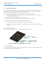
2.2
2.2.1
Hardware Information
Package Details
128-pin Low-Profile Quad Flat Pack (LQFP)
Figure 1 TQFP Mechanical Details
Page 4
(Subject to Change)
DVSI CONFIDENTIAL PROPRIETARY
AMBE-3000F™ Vocoder Chip Users Manual
Version 3.4, April, 2014
2.2.2
Hardware Information
179 Pin Ball Grid Array (BGA)
Figure 2 BGA Mechanical Details
Page 5
(Subject to Change)
DVSI CONFIDENTIAL PROPRIETARY
AMBE-3000F™ Vocoder Chip Users Manual
Version 3.4, April, 2014
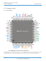
2.3
Pin Assignment Layouts
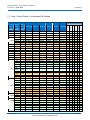
LQFP Package
N/C
Grou nd
1v8
N/C
N/C
S_COM_RAT E2
S_COM_RAT E1
S_COM_RAT E0
Grou nd
N/C
SPI_CLK_IN
I/O Pin (N/C)
I/O Pin (N/C)
3v3
1v8
I/O Pin (N/C)
SPI_FS
PARITY_ENABLE
I/O Pin (N/C)
SPI_GENSTE
I/O Pin (N/C)
STDBY_ENABL E
1v8
Grou nd
I/O Pin (N/C)
I2C_CLK
I2C_DATA
TX_RDY
TX_RQST
I/O Pin (N/C)
I/O Pin (N/C)
I/O Pin (N/C)
2.3.1
Hardware Information
96
Groun d
N/C
N/C
N/C
I/O Pin (N/C)
1v8
Groun d
3v3
N/C
SPI_WAKE
I/O Pin (N/C)
I/O Pin (N/C)
Groun d
1v8
UART_TX
UART_RX
RESET n
1v8
Groun d
N/C
Groun d
3v3
ES_ENABLE
EC_ENABLE
RATE5
RATE4
RATE3
RATE2
RATE1
RATE0
Groun d
Groun d
64
95
94
93
92
91
90
89
88
87
86
85
84
83
82
81
80
79
78
77
76
75
74
73
72
71
70
69
68
67
66
97
65
98
99
100
101
102
103
104
105
106
107
108
109
110
111
112
113
114
115
116
117
118
119
120
121
122
123
124
125
126
127
33
2
3
4
5
6
7
8
9
10
11
12
13
14
15
16
17
18
19
20
21
22
23
24
25
26
27
28
29
30
31
128
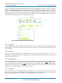
AMBE-3000™ Vocoder Chip
63
62
61
60
59
58
57
56
55
54
53
52
51
50
49
48
47
46
45
44
43
42
41
40
39
38
37
36
35
34
RTS
1v8
Grou nd
RUN
COD EC_RESETn
Grou nd
X1/XCLKIN
X2
1v8
I/O Pin (N/C)
I/O Pin (N/C)
Grou nd
3v3FL
N/C
N/C
3v3
PPT _A CK
PPT _WRITE
PPT _R EAD
IDLE
STAND BY
PKT_RX_WAKE
1v8
PPT _D ATA7
PPT _D ATA6
Grou nd
PPT _D ATA5
PPT _D ATA4
PPT _D ATA3
PPT _D ATA2
PPT _D ATA1
PPT _D ATA0
32
3v3
IF _SELECT0
IF _SELECT1
IF _SELECT2
DT X_ENABLE
SK_ENABLE
NS_ENABLE
CP_ENABLE
CP_SELECT
VREF_1V
VREF_2V
Ground
3v3
3v3
Ground
ADCRESEXT
Ground
McBSP_RxD
McBSP_TxD
1v8
McBSP_CLKR
McBSP_F SX
McBSP_CLKX
McBSP_FSR
3v3
Ground
SPI_CLK
SPI_STE
1v8
Ground
SPI_RX_DATA
SPI_TX_DATA
1
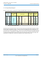
Figure 3 AMBE-3000F™ Vocoder Chip Pins for LQFP Package
All digital inputs are TTL-compatible. All outputs are 3.3 V with CMOS levels. Inputs are not 5-V tolerant. A 100-µA (or 20µA) pullup/pulldown is used. Note that pins 2 through 9 and 119 through 126 do not have internal pullup/pulldowns.
Page 6
(Subject to Change)
DVSI CONFIDENTIAL PROPRIETARY
AMBE-3000F™ Vocoder Chip Users Manual
Version 3.4, April, 2014
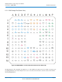
2.3.2
Hardware Information
BGA Package Pins (Bottom View)
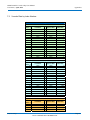
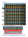
A B C D E F G H J K L M N P
1
2
3
4
5
6
7
8
9
10
11
12
13
14
McBSP
_T xD
IF_
SELECT2
DTX_
ENABL E
CP_
ENABL E
Ground
3v3
IF_
SELECT0
McBSP
NS_
VREF_2V
AD CRESEXT _RxD
ENABL E
RAT E0
Ground
RAT E4
RAT E3
RAT E2
3v3
ES_
ENABL E
1v8
IF_
SK_
SELECT1 ENABL E
3v3
N/C
1v8
McBSP
_CLKX
Ground
1v8
SPI_RX
_DATA
SPI_TX
_DATA
N/C
McBSP
_CL KR
McBSP
_FSR
SPI_
CLK
Ground
N/C
PPT_
DATA0
PPT_
DATA1
Ground
Ground
N/C
N/C
N/C
N/C
N/C
N/C
PPT_
DATA2
PPT_
DATA3
RAT E1
VREF_1V
3v3
Ground
McBSP
_FSX
3v3
SPI_
STE
PPT_
DATA4
PPT_
DATA5
N/C
Ground
Ground
EC_
ENABL E
RAT E5
CP_
SELEC T
N/C
N/C
N/C
PPT_
DATA6
N/C
PKT_RX
_WAKE
PPT_
DATA7
1v8
N/C
Ground
RESET n
N/C
Ground
PPT_
WRIT E
STAND
BY
PPT_
READ
IDLE
UART
_RX
N/C
UART
_T X
N/C
N/C
PPT_
AC K
3v3
N/C
N/C
N/C
N/C
Ground
1v8
I/O Pin
(N/C)
I/O Pin
(N/C)
I/O Pin
(N/C)
I/O Pin
(N/C)
N/C
3v3FL
Ground
N/C
N/C
N/C
SPI_
WAKE
3v3
X1/X
CL KIN
N/C
X2
N/C
1v8
N/C
1v8
Ground
Ground
N/C
S_COM_
RAT E2
I/O Pin
(N/C)
N/C
3v3
Ground
N/C
CODEC_
RESET n
I/O Pin
(N/C)
N/C
N/C
N/C
S_COM_
RAT E1
N/C
3v3
I/O Pin
(N/C)
Ground
N/C
N/C
RU N
N/C
N/C
N/C
N/C
N/C
N/C
1v8
SPI_FS
N/C
1v8
I2C_
DATA
TX_
RQST
RTS
1v8
Ground
N/C
N/C
N/C
S_COM_
RAT E0
SPI_
CL K_IN
Ground
N/C
SPI_
GENST E
Ground
I2C_
CLK
I/O Pin
(N/C)
I/O Pin
(N/C)
N/C
N/C
Ground
1v8
N/C
Ground
I/O Pin
(N/C)
N/C
I/O Pin
(N/C)
Ground
STDBY_
ENABL E
N/C
TX_
RDY
3v3
I/O Pin
(N/C)
I/O Pin
(N/C)
N/C
PARITY_ I/O Pin
ENABLE (N/C)
Figure 4 AMBE-3000F™ Vocoder Chip Pins Bottom View of BGA chip
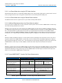
All digital inputs are TTL-compatible. All outputs are 3.3 V with CMOS levels. Inputs are not 5-V tolerant. A 100-µA (or 20µA) pullup/pulldown is used. Note that pins C2, C3, B1, C1, D3, D2, D1, F5, B5, D5, E5, A4, B4, C4, D4, A3 do not have
internal pullup/pulldowns.
Page 7
(Subject to Change)
DVSI CONFIDENTIAL PROPRIETARY
AMBE-3000F™ Vocoder Chip Users Manual
Version 3.4, April, 2014
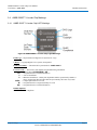
2.4
2.4.1
Hardware Information
AMBE-3000F™ Vocoder Chip Markings
AMBE-3000F™ Vocoder Chip LQFP Markings
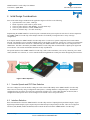
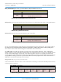
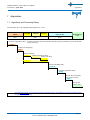
Figure 5 AMBE-3000F™ Vocoder Chip LQFP Markings
DVSI Logo --- Representation of Digital Voice Systems, Inc. Logo.
© DVSI --- Copyright Digital Voice Systems, Incorporated
DVSI Part Number --- The DVSI device part number is AMBE-3000F™
Lot Trace Code --- The lot trace code indicates chip manufacturing information.
Example as shown above CG-58ACRCW 980
CG --- Chip manufacturer’s internal information
5 --- Year of manufacture
8 --- Month of manufacture - January thru September shall be represented by numbers 1
thru 9, and October thru December shall be represented by the letters A, B, and C
ACRC --- Unique alpha-numeric Lot Code
W --- Chip manufacturer’s assigned assembly site code
980 --- Chip manufacturer’s internal information
RoHSCompliance
G4 Indicates RoHS Compliance.
Page 8
(Subject to Change)
DVSI CONFIDENTIAL PROPRIETARY
AMBE-3000F™ Vocoder Chip Users Manual
Version 3.4, April, 2014
2.4.2
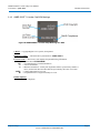
Hardware Information
AMBE-3000F™ Vocoder Chip BGA Markings
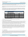
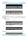
Figure 6 AMBE-3000F™ Vocoder Chip Markings for BGA
© DVSI --- Copyright Digital Voice Systems, Incorporated
DVSI Part Number --- The DVSI device part number is AMBE-3000F™
Lot Trace Code --- The lot trace code indicates chip manufacturing information.
Example as shown above CG-58ACRCW
CG --- Chip manufacturer’s internal information
5 --- Year of manufacture
8 --- Month of manufacture - January thru September shall be represented by numbers 1
thru 9, and October thru December shall be represented by the letters A, B, and C
ACRC --- Unique alpha-numeric Lot Code
W --- Chip manufacturer’s assigned assembly site code
RoHSCompliance
G4 Indicates RoHS Compliance.
Page 9
(Subject to Change)
DVSI CONFIDENTIAL PROPRIETARY
AMBE-3000F™ Vocoder Chip Users Manual
Version 3.4, April, 2014
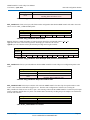
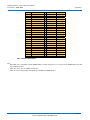
2.5
Hardware Information
Pin Out Table
Pin Name
Pin Number
TQFP BGA
Pin
Type
Notes
IF_SELECT0
IF_SELECT1
IF_SELECT2
DTX_ENABLE
SK_ENABLE
NS_ENABLE
CP_ENABLE
CP_SELECT
2
3
4
5
6
7
8
9
C2
C3
B1
C1
D3
D2
D1
F5
Input
Input
Input
Input
Input
Input
Input
Input
Interface selection configuration
Interface selection configuration
Interface selection configuration
Enables VAD and CNI
Skew Control enable / disable
Noise Suppression enable / disable
Companding enable / disable
Select a-law / µ-law
Voltage Reference Output (1 V). Requires a low ESR (50 mΩ 1.5 Ω) ceramic bypass capacitor of 10 μF to analog ground.
Voltage Reference Output (2 V). Requires a low ESR (50 m Ω 1.5 Ω) ceramic bypass capacitor of 10 μF to analog ground.
VREF_1V
10
E4
-
VREF_2V
11
E2
-
ADCRESEXT
16
F2
-
McBSP_RxD
18
G2
Input
McBSP Serial Packet/Codec Receive Data
McBSP_TxD
19
G1
Output
McBSP Serial Packet/Codec Transmit Data
McBSP_CLKR
21
H2
Input
McBSP_FSX
22
H4
I/O
McBSP_CLKX
23
J1
I/O
McBSP_FSR
24
J2
Input
SPI_CLK
27
K2
Input
SPI_STE
28
K4
Input
SPI_RX_DATA
31
M1
Input
PCM Data from A/D Converter to AMBE-3000F™ Vocoder Chip
SPI_TX_DATA
32
N1
Output
PCM Data from AMBE-3000F™ Vocoder Chip to D/A Converter
PPT_DATA0
33
N2
I/O
Parallel Packet Data
PPT_DATA1
34
P2
I/O
Parallel Packet Data
ADC External Current Bias Resistor (24.9kΩ) to Ground
McBSP Serial Packet/Codec receive clock
McBSP Serial Packet/Codec transmit frame
This signal is an input if the McBSP is used for Codec interface.
This signal is an output if the McBSP is used for Packet interface.
McBSP Serial Packet/Codec transmit clock. This signal is an
Input if the McBSP is used for the Codec Interface. This signal is
an Output if the McBSP is used for Packet interface.
McBSP Serial packet/Codec receive frame
This is the Serial clock from Codec. It also should be connected to
SPI_CLK_IN
This is the framing signal generated from SPI_GENSTE. This pin
need to be connected to Pin #77 on the AMBE-3000F™ Vocoder
Chip.
Page 10
(Subject to Change)
DVSI CONFIDENTIAL PROPRIETARY
AMBE-3000F™ Vocoder Chip Users Manual
Version 3.4, April, 2014
Hardware Information
PPT_DATA2
35
N3
I/O
Parallel Packet Data
PPT_DATA3
36
P3
I/O
Parallel Packet Data
PPT_DATA4
37
L4
I/O
Parallel Packet Data
PPT_DATA5
38
M4
I/O
Parallel Packet Data
PPT_DATA6
40
K5
I/O
Parallel Packet Data
PPT_DATA7
41
N5
I/O
Parallel Packet Data
PKT_RX_WAKE
43
M5
Input
STANDBYn
44
M6
Output
IDLEn
45
P6
Output
PPT_READ
46
N6
Input
PPT_WRITE
47
L6
Input
PPT_ACK
48
K7
Output
3v3FL
52
N8
PWR
X2
57
M9
Output
X1/XCLKIN
58
K9
Input
CODEC_RESETn
60
P10
Output
RUNn
61
P11
Output
When the UART interface is used and low-power mode is enabled,
this pin must be connected to UART_RX. When the McBSP
packet interface is used this signal should be connected to the
inverted McBSP_FSR signal.
For debugging purposes only. This signal is low while the AMBE3000F™ Vocoder Chip is in standby mode. Standby mode is
entered only when Low power mode is enabled and there is no
activity.
For debugging purposes only. This signal is low while the AMBE3000F™ Vocoder Chip is in Idle mode. Idle mode is entered when
there is no activity and low power mode is disabled.
Read data from PACKET_DATA pins
Write data to PACKET_DATA pins
Used to Acknowledges the transitions of PPT_READ and
PPT_WRITE
3.3-V Flash Core Power Pin. This pin should be connected to 3.3
V at all times after power-up sequence requirements have been
met.
Output from internal oscillator for use with a crystal. If the internal
oscillator is not used this pin should be unconnected.
29.4912 MHz Clock input. The AMBE-3000 may be operated
using the internal oscillator by connecting a crystal between X1
and X2 or with an external clock source. The AMBE-3000F™
Vocoder Chip can be operated with an external clock source,
provided that the proper voltage levels are driven on the
X1/XCLKIN pin. It should be noted that the X1/XCLKIN pin is
referenced to the 1.8-V core digital power supply (VDD), rather
than the 3.3-V I/O supply (VDDIO). A clamping diode may be
used to clamp a buffered clock signal to ensure that the logic-high
level does not exceed VDD (1.8 V) or a 1.8-V oscillator may be
used.
Output to Reset the Codec. This signal is active low.
For debugging purposes only. This signal is low while the either
encoder or decoder is executing otherwise it is high.
Page 11
(Subject to Change)
DVSI CONFIDENTIAL PROPRIETARY
AMBE-3000F™ Vocoder Chip Users Manual
Version 3.4, April, 2014
Hardware Information
The Request-To-Send (RTSn) pin is an output that is active low.
The signal is used by the AMBE-3000F™ Vocoder Chip to control
the flow of input packet data. The Chip has a receive buffer where
incoming packets are stored until they have been processed. The
AMBE-3000F™ Vocoder Chip sets RTSn low to indicate that it is
ready to receive data. When RTSn is high, the Chip is not ready to
receive packet data.
RTSn
64
N12
Output
RTSn is set high if there are less than thresh_hi bytes of free space
in the receive buffer. RTSn is set low if there are more than
thresh_lo bytes of free space in the receive buffer. After a reset
thresh_hi is set to 20 and thresh_lo is set to 40, by default. These
thresholds can be changed by sending a PKT_RTSTHRESH field
as part of a control packet after reset. The thresholds may need to
be set to higher values if the device connected to RTSn does not
stop sending packet data quick enough after RTSn goes high.
TX_RQST
68
M12
Input
TX_RDY
69
M14
Output
I2C_DATA
70
L12
Output
The RTSn signal follows the conventions commonly used for RS232 flow control. If the MCBSP or the parallel port is selected for
the packet interface, rather than the UART, then the RTSn signal is
still generated. The RTSn signal can also be used for flow control
if the McBSP or the PPT interface is used.
Channel Transmit Data Strobe TX_RQST is used to control the
encoder timing, when skew control is enabled. It must be high for
at least 250 us. The period must be 20+/-1 ms. When skew
control is enabled the time between rising edges of TX_RQST is
used to determine the number of speech samples per frame.
Transmit Packet Ready goes high as soon as the AMBE-3000F™
Vocoder Chip is ready to transmit a channel packet. Goes low
after the entire packet is read. Regardless of the packet interface
selected, whenever the AMBE-3000F™ Vocoder Chip has a
packet ready for transmission it sets TX_RDY to high.
I2C_DATA (output from AMBE-3000F™ Vocoder Chip to codec)
71
L13
Output
I2C_CLK (output from AMBE-3000F™ Vocoder Chip to codec)
2
I C_CLK
STDBY_ENABLEn is active low and is only used when low
power mode is Enabled. This signal is required for proper function
of low power mode and must be set low at least 500ns prior to
sending a packet to the AMBE-3000F™ Vocoder Chip. If low
power mode is not enabled then signal can be left unconnected and
not used.
STDBY_ENABLEn
75
K14
Input
SPI_GENSTE
77
J13
Output
PARITY_ENABLE
79
H11
Input
Enable parity bit
SPI_FSn
80
H12
Input
SPI_FSn is active low. If the SPI interface is used SPI_FSn must
be connected to the active low frame sync signal from the codec.
SPI_CLK_IN
86
F13
Input
For SPI Interface to function properly this pin must be connected
to the Serial clock from Codec. (pin #27 SPI_CLK)
Required when using the SPI interface. This is used to generate
the SPI_STE signal. This pin should be connected to SPI_STE
(pin# 28).
Page 12
(Subject to Change)
DVSI CONFIDENTIAL PROPRIETARY
AMBE-3000F™ Vocoder Chip Users Manual
Version 3.4, April, 2014
Hardware Information
S_COM_RATE0
89
E13
Input
LSB of Serial Communications Rate selection
S_COM_RATE1
90
E11
Input
Serial Communications Rate selection
S_COM_RATE2
91
F10
Input
MSB of Serial Communications Rate selection
Must be connected to the active low frame sync signal from the
codec if the SPI interface is used and low power mode is enabled.
The signal is used to wake the AMBE-3000F™ Vocoder Chip
from stand-by mode.
SPI_WAKE
106
D9
Input
UART_TX
111
C7
Output
UART_RX
112
A7
Input
RESETn
113
D6
I/O
ES_ENABLE
EC_ENABLE
RATE5
RATE4
RATE3
RATE2
RATE1
RATE0
119
120
121
122
123
124
125
126
B5
D5
E5
A4
B4
C4
D4
A3
Input
Input
Input
Input
Input
Input
Input
Input
Echo Suppressor enable / disable
Echo Canceller enable / disable
Vocoder Bit Rate Control Word
Vocoder Bit Rate Control Word
Vocoder Bit Rate Control Word
Vocoder Bit Rate Control Word
Vocoder Bit Rate Control Word
Vocoder Bit Rate Control Word
20, 29,
42, 56,
63, 74,
82, 94,
102,
110,
114
B10,
C8,
C14,
G12,
H1,
K12,
L1,
P5,
P9,
P12,
A6
PWR
Supply Voltage 1.8-V Core Digital Power Pins. (VDD)
1v8
Channel Transmit Data from AMBE-3000F™ Vocoder Chip SCI
asynchronous serial port. This pin must be held HIGH during a
Hard Reset.
Channel Receive Data to AMBE-3000F™ Vocoder Chip
asynchronous serial port.
AMBE-3000F™ Vocoder Chip Reset pin. Active LOW. The
RESET pin is considered an I/O port and will function as such
when a SOFT RESET packet (PKT_RESET or
PKT_RESETSOFTCFG) is sent to the device. For more details
see Section 3.6 Reset Behavior
Page 13
(Subject to Change)
DVSI CONFIDENTIAL PROPRIETARY
AMBE-3000F™ Vocoder Chip Users Manual
Version 3.4, April, 2014
3v3
Ground
I/O Pin
1, 13,
14, 25,
49, 83,
104,
118
12, 15,
17, 26,
30, 39,
53, 59,
62, 73,
88, 95,
97,
103,
109,
115,11
7, 127,
128
54, 55,
65, 66,
67, 72,
76, 78,
81, 84,
85,
101,
107,
108
Hardware Information
B2,
E1,
F4,
E9,
G11,
J4,
L7,
A5,
L10,
N14,
PWR
3.3 V I/O Digital Power Pins.
E3,
F3,
B8,
B14,
C10,
D10,
E14,
G4,
G13,
J14,
K1,
K6,
A13,
K13,
L2,
C6,
C5,
B3,
A2,
L11,
M10,
P4,
P8,
GND
Core and Digital I/O Pins to Ground. (VSS)
L8,
K8,
N13,
P14,
M13,
K11,
J11,
H10,
H14,
G10,
F14,
A11,
E8,
D8
I/O
No Connection
Page 14
(Subject to Change)
DVSI CONFIDENTIAL PROPRIETARY
AMBE-3000F™ Vocoder Chip Users Manual
Version 3.4, April, 2014
N/C
50, 51,
87, 92,
93, 96,
98, 99,
100,
105,
116
N7,
M7,
F11,
D13,
D12,
C13,
B12,
A12,
D11,
C9,
E6
Hardware Information
-
No Connection
Page 15
(Subject to Change)
DVSI CONFIDENTIAL PROPRIETARY
AMBE-3000F™ Vocoder Chip Users Manual
Version 3.4, April, 2014
B6,
B13,
E7,
F1,
K10,
M3,
N4,
N11,
P1,
P13,
A8,
A10,
A14,
B7,
B9,
C11,
C12,
D7,
D14,
E10,
E12,
F12,
G5,
G14,
H13,
J12,
M2,
M11,
N10,
A9,
B11,
G3,
H3,
H5,
J3,
J5,
J10,
K3,
L3,
L5,
L9,
L14,
M8,
N9,
P7,
N/C
Hardware Information
-
No Connection
Table 1 Pinout List
NOTE:
Other than the power supply pins, no pin should be driven before the 3.3-V rail has reached recommended operating
conditions. However, it is acceptable for an I/O pin to ramp along with the 3.3-V supply.
The following pins have internal pullup
18/G2, 21/H2, 22/H4, 23/J1, 24/J2, 33/N2, 34/P2, 35/N3, 36/P3, 37/L4, 38/M4, 40/K5, 41/N5, 43/M5, 44/M6, 45P6, 46/N6,
47/L6, 48/K7, 54/L8, 55/K8, 60/P10, 61/P11, 64/N12, 65/N13, 68/M12, 69/M14, 70/L12, 71/L13, 72/K11, 75/K14, 76/J11,
Page 16
(Subject to Change)
DVSI CONFIDENTIAL PROPRIETARY
AMBE-3000F™ Vocoder Chip Users Manual
Version 3.4, April, 2014
Hardware Information
77/J13, 78/H10, 79/H11, 80/H12, 81/H14, 84/G10, 85/F14, 86/F13, 89/E13, 90/E11, 91/F10, 92/D13, 96/C13, 99/A12,
100/D11, 101/A11, 105/C9, 107/E8, 111/C7, 112/A7, 113/D6
The following pins have internal Pulldown
98/B12
Page 17
(Subject to Change)
DVSI CONFIDENTIAL PROPRIETARY
AMBE-3000F™ Vocoder Chip Users Manual
Version 3.4, April, 2014
2.6
Hardware Information
Hardware Configuration Pins
There is a set of configuration pins that allows the user to set-up the most common chip configurations. The chip boots up
according to the configuration pins. Then after booting up, if any configuration packets are received, the configuration is
changed accordingly. The configuration pins are only checked at boot time.
Hardware Configuration Pins
Pin Number
TQFP
BGA
Name
Description
2
3
4
C2
C3
B1
IF_SELECT0
IF_SELECT1
IF_SELECT2
5
6
7
C1
D3
D2
DTX_ENABLE
SK_ENABLE
NS_ENABLE
See Section 4.5.4
See Section 4.5.5
See Section 4.5.6
8
9
D1
F5
CP_ENABLE
CP_SELECT
See Section 4.5.7
79
H11
PARITY_ENABLE
See Section 6.5.5
89
90
91
E13
E11
F10
S_COM_RATE0
S_COM_RATE1
S_COM_RATE2
119
120
121
122
123
124
125
126
B5
D5
E5
A4
B4
C4
D4
A3
ES_ENABLE
EC_ENABLE
RATE5
RATE4
RATE3
RATE2
RATE1
RATE0
See Section 4.2
See Table 20 UART Baud Rates
Echo suppressor enable Pin
Echo Cancellation enable Pin
See Table 116 Rate Control Words and Pin
Settings
Table 2 Hardware Configuration Settings
Page 18
(Subject to Change)
DVSI CONFIDENTIAL PROPRIETARY
AMBE-3000F™ Vocoder Chip Users Manual
Version 3.4, April, 2014
2.7
Hardware Information
Crystal / Oscillator Usage
The AMBE-3000F™ Vocoder Chip has an on-chip, PLL-based clock module and requires an input clock frequency of 29.4912
MHz. The PLL-based clock module provides all the necessary clocking signals for the device, as well as control for lowpower mode entry. The AMBE-3000F™ Vocoder Chip two modes of operation:
External clock source operation (See Figure 7 X1/XCLKIN and X2 with TTL/CMOS Clock Source)
This mode allows the internal oscillator to be bypassed. The device clocks are generated from an external clock
source input on the X1/XCLKIN pin.
Crystal-operation (See Figure 8 X1/XCLKIN and X2 with Crystal Oscillator)
This mode allows the use of an external crystal/resonator to provide the time base to the device.
The following points should be noted when designing any printed circuit board layout:
Keep X1/XCLKIN and X2 away from high frequency digital traces to avoid coupling.
Keep the crystal and external capacitors as close to the X1/XCLKIN and X2 pins as possible to minimize board stray
capacitance.
2.7.1
External Clock Source
When an external source is used as the clock input. Connect X1/XCLKIN and X2 as follows:
Figure 7 X1/XCLKIN and X2 with TTL/CMOS Clock Source
2.7.2
Crystal Oscillator
To use a crystal oscillator with the AMBE-3000F™ Vocoder Chip, connect the crystal across X1/XCLKIN and X2 along with
one external capacitor from each of these pins to ground.
Page 19
(Subject to Change)
DVSI CONFIDENTIAL PROPRIETARY
AMBE-3000F™ Vocoder Chip Users Manual
Version 3.4, April, 2014
Hardware Information
Figure 8 X1/XCLKIN and X2 with Crystal Oscillator
NOTE A: It is recommended that the resonator/crystal vendor characterize the operation
of their device with the chip. The resonator/crystal vendor has the equipment and
expertise to tune the tank circuit. The vendor can also advise regarding the proper tank
component values that will ensure start up and stability over the entire operating range.
The typical specifications for the external quartz crystal for a frequency of 30 MHz are listed below:
Fundamental mode, parallel resonant
CL (load capacitance) = 12 pF
CL1 = CL2 = 24 pF
Cshunt = 6 pF
ESR range = 25 to 40 Ohms
2.7.3
Input Clock Requirements
The clock provided at XCLKIN pin generates the internal CPU clock cycle.
ID
A
B
C
VIH
VIL
Parameter
tc(Cl) Cycle time, XCLKIN
tr(Cl) Rise time, XCLKIN
tf(Cl) Fall time, XCLKIN
tw(ClL) Pulse duration XCLKIN Low as a percentage of tc(Cl)
tw(ClH) Pulse duration XCLKIN High as a percentage of tc(Cl)
Parameter
High-level input voltage X1/XCLKIN (@50uA max)
Low-level input voltage X1/XCLKIN (@50uA max)
Min
.7 (1v8)
Min.
6.67
40
40
Nom
-
Max.
250
6
6
60
60
Unit
ns
ns
ns
%
%
Max
1v8
0.3 (1v8)
Unit
V
V
Figure 9 Input Clock Requirements
Page 20
(Subject to Change)
DVSI CONFIDENTIAL PROPRIETARY
AMBE-3000F™ Vocoder Chip Users Manual
Version 3.4, April, 2014
Digital Voice Systems, Inc.
The Speech Compression Specialists
Electrical Characteristics and Requirements
3 Electrical Characteristics and Requirements
Unless otherwise noted, the list of absolute maximum ratings is specified over operating temperature ranges. Stresses beyond
those listed under Absolute Maximum Ratings may cause permanent damage to the device. These are stress ratings only and
functional operation of the device at these or any other conditions beyond those indicated are not implied. Exposure to
absolute-maximum-rated conditions for extended periods may affect device reliability. All voltage values are with respect to
Vss.
3.1
Normal Operating Conditions
Normal Operating Conditions
Operating Voltage
1.8-V Core, (135 MHz), 3.3-V I/O
Operating Ambient Temperature Range
-40C to 85C
Storage Temperature Range
-65C to 150C
Junction Temperature Range
-40C to 150C
Table 3 Normal Operating Conditions
Long-term high-temperature storage and/or extended use at maximum temperature conditions may result in a reduction of
overall device life. For additional information, see IC Package Thermal Metrics Application Report (TI literature number
SPRA953) and Reliability Data for additional information; see IC Package Thermal Metrics Application Report and Reliability
Data (TI literature number SPRA953).
3.2
Recommended Operating Conditions
3v3
1v8
VIH
VIL
VIH
VIL
fSYSCLKOUT
IOH
IOH
IOL
IOL
Parameter
Device Supply Voltage, I/O
Device Supply Voltage, CPU 1.8 V (135MHz)
High-level input voltage All inputs except X1/XCLKIN
Low-level input voltage All inputs except X1/XCLKIN
High-level input voltage X1/XCLKIN (@50uA max)
Low-level input voltage X1/XCLKIN (@50uA max)
Device clock frequency (system clock) = 1.8 V ± 5%
High-level output current source current, VOH = 2.4 V
High-level output current source current, VOH = 2.4 V (See
Note) ††
Low-level output sink current VOL = VOL MAX
Low-level output sink current VOL = VOL MAX (Group 2)
Min
3.14
1.71
2.0
.7(1v8)
Nom
3.3
1.8
0.8
29.4912
-4
Max
3.47
1.89
3v3
1v8
0.3(1v8)
Unit
V
V
V
V
V
V
MHz
mA
-8
mA
4
8
mA
mA
Table 4 Recommended Operating Conditions
†† Note Applies to the following pin: SPI_WAKE (TQFP Pin 106, BGA Pin D9).
3.3
Absolute Maximum Ratings
Stresses in excess of the Absolute Maximum Ratings can cause permanent damage to the device. These are absolute stress
ratings only. Functional operation of the device is not implied at these or any other conditions in excess of those given in the
Page 21
(Subject to Change)
DVSI CONFIDENTIAL PROPRIETARY
AMBE-3000F™ Vocoder Chip Users Manual
Version 3.4, April, 2014
Electrical Characteristics and Requirements
operational sections of the data sheet. Exposure to Absolute Maximum Ratings for extended periods can adversely affect
device reliability.
Absolute Maximum Ratings
3v3 Supply voltage range
1v8 Supply voltage range
Input voltage range,VIN
Output voltage range, VO
Input clamp current IIK (VIN < 0 or VIN > 3v3)†
Output clamp current IOK (VO < 0 or VO > 3v3)
-0.3 V to 4.6 V
-0.5 V to 2.5 V
-0.3 V to 4.6 V
-0.3 V to 4.6 V
± 20 mA
± 20 mA
Table 5 Absolute Maximum Ratings
†Continuous clamp current per pin is ± 2 mA
3.4
Thermal Resistance Characteristics
Thermal Resistance Characteristics
Package Type
Parameter
TQFP
BGA
PsiJT
0.271
0.658
41.65
42.57
ΘJA
10.76
16.08
ΘJC
Unit
C/W
C/W
C/W
Table 6 Thermal Resistance Characteristics
Unless otherwise noted, the list of absolute maximum ratings is specified over operating temperature ranges. All voltage values
are with respect to Vss.
3.5
Power Sequencing Requirements
The AMBE-3000F™ Vocoder Chip silicon requires dual voltages (1.8-V and 3.3-V) to power up the CPU, Flash, ROM, ADC,
and the I/Os. To ensure the correct reset state for all modules during power up, there are some requirements to be met while
powering up/powering down the device.
Enable power to all 3.3-V supply pins and then ramp 1.8 V supply pins (Table 7 Voltage Supply Pins). Other than the power
supply pins, no pin should be driven before the 3.3-V rail has been fully powered up.
Voltage Supply Pins
Package Type
3.3 V Supply Pins
TQFP
1, 13, 14, 25, 49, 83, 104, 118
BGA
B2, E1, F4, E9, G11, J4, L7, A5, L10, N14
1.8 V Supply Pins
20, 29, 42, 56, 63, 74, 82, 94, 102, 110, 114
B10, C8, C14, G12, H1, K12, L1, P5, P9,
P12, A6
Table 7 Voltage Supply Pins
Page 22
(Subject to Change)
DVSI CONFIDENTIAL PROPRIETARY
AMBE-3000F™ Vocoder Chip Users Manual
Version 3.4, April, 2014
Electrical Characteristics and Requirements
1.8 V supply voltage should not reach 0.3 V until 3v3 has reached 2.5 V. This ensures the reset signal from the I/O pin has
propagated through the I/O buffer to provide power-on reset to all the modules inside the device.
In other words, 3.3-V and 1.8-V can ramp together.
3.6
Reset Behavior
To avoid startup latency problems the system should be designed to supply a cascading reset. This means that once the system
host processor is fully functional it should bring the AMBE-3000™ Vocoder Chip out of reset using RESETn signal. The
AMBE-3000™ Vocoder Chip should then supply the CODEC_RESETn signal to bring the codec out of reset. Employing
reset in this cascading fashion will allow each device to be up and running in proper sequence so that no data is lost.
AMBE-3000™
Host
Processor
RESET*
RESETn
Pin
113 (D6)
Pin
60 (P10)
Codec
RESET*
CODEC _RESETn
Figure 10 Cascading Resets
Care should be taken with the AMBE-3000™ Vocoder Chip RESET pin (LQFP pin 113, BGA pin D6). The RESET pin is
considered an I/O port and will function as such when a SOFT RESET packet (PKT_RESET or PKT_RESETSOFTCFG) is
sent to the device. This means that when a SOFT RESET packet is issued, the AMBE-3000™ Vocoder Chip will pull the
RESET pin low for a short period of time (approximately 20 µsec). The designer should avoid having the AMBE-3000™
Vocoder Chip’s RESET pin be shared on the system reset line or a reset with other components on the board if there is a
chance that a SOFT RESET may be called for in the design.
3.6.1
Reset to Ready Packet Timing
RESET release to PKT_ READY is 20 msec MAX, 17 msec TYPICAL.
SOFT reset to PKT_READY = ~ 7 msec
3.6.2
Behavior of RTSn and TX_RDY following a RESET
Following a RESET, there is a short period where the TX_RDY signal is set high by the AMBE-3000. During this short period
reading of the TX_RDY should be avoided. The TX_RDY hold off period is approximately 1 msec following a reset.
Page 23
(Subject to Change)
DVSI CONFIDENTIAL PROPRIETARY
AMBE-3000F™ Vocoder Chip Users Manual
Version 3.4, April, 2014
Electrical Characteristics and Requirements
“Re set a cti vated”
RESETn
A
B
A
B
C
RTS
C
TX_RDY
A
B
C
Figure 11 TX_RDY after Reset
3.7
Signal Transition Levels
Note that some of the signals use different reference voltages, see Table 4 Recommended Operating Conditions. Output levels
are driven to a minimum logic-high level of 2.4 V and to a maximum logic-low level of 0.4 V.
Figure 12 Output Levels
Output transition times are specified as follows:
For a high-to-low transition, the level at which the output is said to be no longer high is below VOH(MIN) and the level
at which the output is said to be low is VOL(MAX) and lower.
For a low-to-high transition, the level at which the output is said to be no longer low is above VOL(MAX) and the level
at which the output is said to be high is VOH(MIN) and higher.
Page 24
(Subject to Change)
DVSI CONFIDENTIAL PROPRIETARY
AMBE-3000F™ Vocoder Chip Users Manual
Version 3.4, April, 2014
Electrical Characteristics and Requirements
Figure 13 Input Levels
Input levels are as follows 0.8 V (VIL) and 2.0 V (VIH)
Input transition times are specified as follows:
For a high-to-low transition on an input signal, the level at which the input is said to be no longer high is below
VIH(Min) and the level at which the input is said to be low is VIL(Max) and lower.
3.8
For a low-to-high transition on an input signal, the level at which the input is said to be no longer low is above
VIL(Max) and the level at which the input is said to be high is VIH(Min) and higher.
Power-Down Sequencing:
During power-down, the device reset should be asserted low (8 μs, minimum) before the 1.8 V supply reaches 1.5 V. This will
help to keep on-chip flash logic in reset prior to the 3v3and 1.8 V power supplies ramping down. It is recommended that the
device reset control from “Low-Dropout (LDO)” regulators or voltage supervisors be used to meet this constraint. LDO
regulators that facilitate power-sequencing (with the aid of additional external components) may be used to meet the power
sequencing requirement.
3.9
Low Power Modes
The AMBE-3000F™ Vocoder Chip has four power states as shown in Figure 14 AMBE-3000F™ Vocoder Chip Power States.
Figure 14 AMBE-3000F™ Vocoder Chip Power States
Page 25
(Subject to Change)
DVSI CONFIDENTIAL PROPRIETARY
AMBE-3000F™ Vocoder Chip Users Manual
Version 3.4, April, 2014
Electrical Characteristics and Requirements
In order to reduce power consumption the AMBE-3000F™ Vocoder Chip automatically switches to lower power states when
possible. The AMBE-3000F™ Vocoder Chip may switch power states many times during each 20 ms frame. For instance,
during periods when the AMBE-3000F™ Vocoder Chip is not actively executing code, the AMBE-3000F™ Vocoder Chip
will be in a low power state. When a codec interrupt occurs the AMBE-3000F™ Vocoder Chip will briefly switch into the run
state and then switch back to the lower power state. If the codec interface is in use, then the AMBE-3000F™ Vocoder Chip
will never remain in the low power state for more than 125 us at a time.
Figure 15 Power Mode States Basic Timing
3.9.1
Run State
This is the highest power state. The AMBE-3000F™ Vocoder Chip is in this state whenever it is actively executing code. The
AMBE-3000F™ Vocoder Chip is in the run state if the encoder is running or if the decoder is running or other processing is
being performed.
3.9.2
Idle State
This state uses less power than the run state. The AMBE-3000F™ Vocoder Chip is in this state whenever it is not actively
executing code, but peripherals are active. Peripherals are active when packets are being transmitted or received or when codec
samples are being clocked in/out.
3.9.3
Standby State
This state uses even less power than the Idle State. However, no peripherals can be sending or receiving data while in this
state. The AMBE-3000F™ Vocoder Chip will only enter this state if low power mode is enabled, AND the AMBE-3000F™
Vocoder Chip is not actively executing code, AND no peripherals are in use. Peripheral activity causes the AMBE-3000F™
Vocoder Chip to re-enter the run state. When low power mode is enabled, some extra hardware connections are required. The
required connections are dependent upon which interfaces are in use.
3.9.4
Halt State
This is the lowest power state. The AMBE-3000F™ Vocoder Chip does not automatically enter in and out of this state. The
only way to get into this state is to send a packet containing a PKT_HALT field. The only way to get out of this state is via a
hard reset. During a hard reset be sure to hold UART_TX HIGH (LQFP pin 111, BGA pin C7)
Page 26
(Subject to Change)
DVSI CONFIDENTIAL PROPRIETARY
AMBE-3000F™ Vocoder Chip Users Manual
Version 3.4, April, 2014
3.9.5
Electrical Characteristics and Requirements
Power Modes
The AMBE-3000F™ Vocoder Chip has two power modes:
(1) Normal Power Mode: In this mode the AMBE-3000F™ Vocoder Chip switches between the Run State and the Idle
State.
(2) Low Power Mode: In this mode the AMBE-3000F™ Vocoder Chip switches between the Run State, the Idle State,
and the Standby State. Lower power is consumed because the AMBE-3000F™ Vocoder Chip is in the Standby state
a large percentage of the time. low power mode is enabled or disabled by sending a packet containing
PKT_LOWPOWER field to the AMBE-3000F™ Vocoder Chip. After reset, low power mode is always disabled.
Figure 16 Power Modes
The AMBE-3000F™ Vocoder Chip outputs three signals that are related to its current power state. The STANDBYn (TQFP
pin 44 / BGA pin M6) signal goes low whenever the AMBE-3000F™ Vocoder Chip is in the Standby State, otherwise the
signal is high. The IDLEn (TQFP pin 45 / BGA pin P6) signal is low whenever the AMBE-3000F™ Vocoder Chip is in the
Idle State, otherwise the signal is high. The RUNn (TQFP pin 61 / BGA pin P11) signal is low whenever, either the encoder or
the decoder is running, otherwise the signal is high.
3.9.6
Low power mode when using the UART Packet Interface
When the UART packet interface is used and low-power mode is enabled, PKT_RX_WAKE (TQFP pin 43 / BGA pin M5)
must be connected to UART_RX (TQFP pin 112 / BGA pin A7). The signal is used to make sure that the standby state is not
entered while UART_RX is active.
3.9.7
Low Power Mode when using the McBSP Packet Interface
When the McBSP packet interface is used the PKT_RX_WAKE (TQFP pin 43 / BGA pin M5) signal must be connected to the
inverted McBSP_FSR signal (TQFP pin 24 / BGA pin J2). The signal is needed in order to wake the chip from the standby
state.
3.9.8
Low Power Mode when using the McBSP Codec Interface
When the McBSP codec interface is used the SPI_WAKE (TQFP pin 106 / BGA pin D9) signal must be connected to the
inverted McBSP_FSR signal (TQFP pin 24 / BGA pin J2). The signal is needed in order to wake the chip from the standby
state.
Note: The higher the frequency of the MCBSP clock the better power consumption will be when low-power mode is enabled.
Page 27
(Subject to Change)
DVSI CONFIDENTIAL PROPRIETARY
AMBE-3000F™ Vocoder Chip Users Manual
Version 3.4, April, 2014
3.9.9
Electrical Characteristics and Requirements
Low Power Mode when using the SPI Codec Interface
When the SPI codec interface is used the SPI_WAKE (TQFP pin 106 / BGA pin D9) signal must be connected to the inverted
frame sync signal from the codec. The signal is needed in order to wake the chip from the standby state.
3.9.10 Low Power Mode when using the Parallel Packet Interface
No additional connections are required to use low power mode with the parallel interface.
3.9.11 Additional Requirements when Low Power Mode is enabled.
If low power mode is enabled, there are some restrictions on when a packet can be sent to the AMBE-3000F™ Vocoder Chip.
One of the following methods most be chosen.
Method 1: Prior to the start of any packet transfer to the AMBE-3000F™ Vocoder Chip, the STDBY_ENABLEn (TQFP pin
75 / BGA pin K14) pin must be set low at least 500ns prior to sending the first byte of a packet via UART, McBSP, or Parallel
Port. The signal should be set high anytime after the first byte of the packet has been transferred to the AMBE-3000F™
Vocoder Chip. When the STDBY_ENABLEn is held low, the AMBE-3000F™ Vocoder Chip is prevented from entering the
standby state, so it is important that the STDBY_ENABLEn signal is set high prior to the end of the last byte of the packet.
OR
Method 2: STDBY_ENABLEn (TQFP pin 75 / BGA pin K14) must be pulled high or left disconnected. Prior to the start of
any packet transfer to the AMBE-3000F™ Vocoder Chip, wait for a transition of the STANDBYn (TQFP pin 44 / BGA pin
M6) signal from the high state to the low state. After the transition is detected begin sending the first byte of the packet to the
AMBE-3000F™ Vocoder Chip via UART, McBSP, or Parallel Port within 100µs after the transition was detected.
OR
Method 3: A packet may be sent to the AMBE-3000F™ Vocoder Chip at anytime after the AMBE-3000F™ Vocoder Chip has
begun transmitting a packet up until the time the AMBE-3000F™ Vocoder Chip has just finished transmitting the packet. It is
important that the first byte of the packet being sent to the AMBE-3000F™ Vocoder Chip be sent before the last byte of the
packet is received from the AMBE-3000F™ Vocoder Chip.
3.9.12 Typical AMBE-3000F™ Vocoder Chip Power Measurements:
Test Conditions
Power Measurement
Low Power Mode NOT Enabled
Low Power Mode Enabled
Codec Mode (SPI Interface)
UART Packet Interface
50% Voice Activity
1.8v uses 154 mW
3.3v uses 26 mW
Packet Mode
UART Packet Interface
Not receiving packets
125 mW
(AMBE-3000F™ Vocoder Chip
is in the idle state)
Maximum Current Values
Total
180 mW
1.8v uses 62 mW
3.3v uses 23 mW
Total
85 mW
(DTX enabled)
22 mW
(AMBE-3000F™ Vocoder Chip is in
the standby state)
1.8v = 193 mW
3.3v = 171 mW
Table 8 Typical AMBE-3000F™ Vocoder Chip Power Measurements
Page 28
(Subject to Change)
DVSI CONFIDENTIAL PROPRIETARY
AMBE-3000F™ Vocoder Chip Users Manual
Version 3.4, April, 2014
Electrical Characteristics and Requirements
Page 29
(Subject to Change)
DVSI CONFIDENTIAL PROPRIETARY
Digital Voice Systems, Inc.
AMBE-3000F™ Vocoder Chip Users Manual
Version 3.4, April, 2014
The Speech Compression Specialists
Initial Design Considerations
4 Initial Design Considerations
Some of the initial design considerations the application engineer will face are the following:
Speech and FEC rates. (2000 – 9600 bps)
Mode of operation (codec mode or packet mode)
Choice of codec interface. (SPI, McBSP) - for codec mode only!
Choice of packet interface. (UART, McBSP, PPT)
Choice of A/D-D/A chip. - for codec mode only!
Implementing the AMBE-3000F™ Vocoder Chip into a communication system requires the selection of various components.
The AMBE-3000F™ Vocoder Chip offers multiple interfaces for flexibility in integration into a variety of design
configurations.
In its simplest model, the AMBE-3000F™ Vocoder Chip can be viewed as two separate components, the Encoder and the
Decoder. The Encoder receives an 8 kHz sampled stream of speech data (16-bit linear, 8-bit A-law, or 8-bit µ-law) and outputs
a stream of channel data at the desired rate. Simultaneously, the AMBE-3000F™ Vocoder Chip receives compressed voice
channel data. This data is decoded by the AMBE-3000F™ Vocoder Chip, then reconstructed into a digital speech signal and
sent to the D/A. The encoder and decoder functions are fully asynchronous.
The special functions of the AMBE-3000F™ Vocoder Chip, such as echo cancellation, voice activity /detection, power mode
control, data/FEC rate selection, etc. can be controlled either through hardware control pins and/or through the packet interface.
Figure 17 Basic Operation
4.1
Vocoder Speech and FEC Rate Selection
The voice coding rate as well as the FEC coding rate can be selected individually on the AMBE-3000F™ Vocoder Chip.
These rates are selected by using a configuration control packet, or through hardware configuration pins. The hardware
configuration pins provide the user with 62 pre-configured voice/FEC rates. If rates other than these are desired, then a
configuration control packet can be used to configure voice and FEC rates in 50 bps increments.
4.2
Interface Selection
Basic communication to/from the AMBE-3000F™ Vocoder Chip consists of input digitized speech data samples, output
digitized speech data samples, input compressed speech data and output compressed speech data. There are four physical
interfaces (SPI, McBSP, UART and Parallel) used to transfer the data to/from the AMBE-3000F™ Vocoder Chip.
Page 30
(Subject to Change)
DVSI CONFIDENTIAL PROPRIETARY
AMBE-3000F™ Vocoder Chip Users Manual
Version 3.4, April, 2014
Initial Design Considerations
For codec mode, the user must select two physical interfaces: one for the codec data and one for the packet data. The choices
for the codec interface are SPI or McBSP. The choices for the packet interface are McBSP or UART or Parallel Port. The
McBSP can not be used for both the codec interface and the packet interface.
For packet mode, the user must select one physical interface to be used for packet data. The packet interface is used to transfer
both the speech data samples and the compressed channel data. The choices for the packet interface are McBSP or UART or
Parallel Port.
The AMBE-3000F™ Vocoder Chip supports four separate physical interfaces: SPI, UART, Parallel port, and McBSP serial
port. The user must select a codec interface and a packet interface using hardware configuration pins IF_SELECT0 (TQFP
pin2, BGA pin C2), IF_SELECT1 (TQFP pin3, BGA pin C3), and IF_SELECT2 (TQFP pin4, BGA pin B1). The available
interface combinations are shown in Table 9 Physical Interface Selection
Interface Configurations
IF_SELECT Configuration
Pin #’s (TQFP / BGA)
Mode
4 / B1
3 / C3
2 / C2
Codec Mode
0
0
0
Codec Mode
0
0
1
Codec Mode
0
1
0
Codec Mode
0
1
1
Codec Mode
1
0
0
Packet Mode
1
0
1
Packet Mode
1
1
0
Packet Mode
1
1
1
Codec Interface
Packet Interface
SPI
SPI
SPI
McBSP*
McBSP*
Not used
Not used
Not used
UART
PPT
McBSP*
UART
PPT
UART
PPT
McBSP*
Table 9 Physical Interface Selection
*Note: McBSP Interface may be used for codec interface or the packet interface but not both.
4.3
A/D – D/A Codec chip Selection
The AMBE-3000F™ Vocoder Chip can be configured to transmit and receive digitized speech to and from most linear, a-law,
or u-law A/D-D/A codecs. The format of the incoming and outgoing speech data streams are coupled, that is to say they must
be the same format (16-bit linear, 8-bit a-law, or 8-bit -law). The digitized speech from the external A/D is converted into
compressed digital data (encoded) by the AMBE-3000F™ Vocoder Chip and the channel data is output to the packet interface.
Alternatively, speech data can be sent to/from the AMBE-3000F™ Vocoder Chip via a packet interface.
The choice of the A/D-D/A chip is critical to designing a system with superior voice quality. Given that a-law and -law
companding chips are already incorporating some compression to reduce the number of bits per sample, it is recommended
that, when possible, a 16-bit linear device be used for maximum voice quality. When choosing a device, pay particular
attention to signal to noise ratios and frequency responses of any filters that may be present on the analog front end of these
chips. Generally speaking, the flatter the frequency response over the voice spectrum (20-4000Hz) the better the overall
system will sound. The a-law and law interfaces are mainly provided for the design engineer who is trying to fit to preexisting conditions or is under cost savings restraints.
4.4
Vocoder State
In systems that require the ability to encode/decode different subsequent audio streams the vocoder state in the AMBE-3000™
Vocoder Chip would need to be reset back to the initial state. This will ensure that new audio streams will not be using state
data from a previous unrelated audio stream. To clear out any old vocoder state information the designer should send a
PKT_INIT to the AMBE-3000™ Vocoder Chip in between each different audio stream. This will reset the chip back to the
default state and allow it to encode/decode properly.
Page 31
(Subject to Change)
DVSI CONFIDENTIAL PROPRIETARY
AMBE-3000F™ Vocoder Chip Users Manual
Version 3.4, April, 2014
Initial Design Considerations
Issue a PKT_CODECSTOP:
0x61 0x00 0x01 0x2B
Issue PKT_INIT:
0x61 0x00 0x02 0x0B 0x03
Issue a PKT_CODECSTART
0x61 0x00 0x02 0x00 0x2A XxXX*
*See Table 57 PKT_CODECSTART Field Data
4.5
Special Functions Description
The special functions of the AMBE-3000F™ Vocoder Chip, such as voice activity detection, echo cancellation, DTMF,
data/FEC rate selection, power mode control, etc. can be controlled either through hardware control pins and/or through the
packet interface. The hardware inputs are only accessed for input during the first 7 milliseconds after a hardware reset on
RESETn. For predictable operation these signals must remain stable over this time period. After this 7 milliseconds
initialization period changes on these pins are ignored, unless another reset is performed.
4.5.1
Voice Activity Detection & Comfort Noise Insertion
(DTX_ENABLE TQFP pin5, BGA pin C1)
The Voice Activity Detection (VAD) algorithm along with the Comfort Noise Insertion (CNI) feature of the AMBE-3000F™
Vocoder Chip performs useful functions in systems trying to convert periods of silence, that exist in normal conversation, to
savings in system bandwidth or power. VAD and CNI can be enabled by either hardware configuration pin (DTX_ENABLE
TQFP pin5 BGA pin C1) or as part of a control packet.
With the VAD functions enabled, when periods of silence occur, the encoder will output a silence frame (in-band). This
silence frame contains information regarding the level of background noise, which allows the corresponding decoder to
synthesize a “Comfort Noise” signal at the other end. The comfort noise is intended to give the listener the feeling that the call
is still connected, as opposed to producing absolute silence, which can give the impression that, the call has been “dropped”.
The decoder will produce a comfort noise frame if it receives an in-band silence frame (produced only by an encoder with
VAD enabled). The synthesis of a Comfort Noise frame by the decoder is not dependent on VAD being enabled.
If the VAD features are being used to reduce transmit power during times of conversational silence, DVSI recommends that a
silence frame be transmitted at the start of the period and approximately each 500-1000 milliseconds thereafter. This is to
ensure that the parameters regarding the levels of background noise are transmitted to the decoder for the smoothest audible
transitions between synthesized speech and synthesized silence.
The silence threshold value is -25 dBm0 in the VAD algorithm. Each frame that exceeds this level will be classified as voice.
If the frame level is less than -25 dBm0 the voice/silence decision will be determined based upon various adaptive thresholds.
4.5.2
Echo Canceller (EC_ENABLE TQFP pin120 BGA pin D5)
The AMBE-3000F™ Vocoder Chip’s voice coder contains an echo canceller that can be selectively enabled or disabled via
either hardware pin or setting of control command packet. The echo canceller is suitable for canceling the local echo caused by
a 2-to-4 wire hybrid and can achieve echo cancellation of approximately 30dB or more. Only the linear portion of the echo can
be cancelled, so circuits should be designed to minimize nonlinearities. The Echo Return Loss (ERL) of the analog circuit
must be 6dB or more for proper echo canceller operation. Linear Codecs will generally provide better performance than µ-law
or a-law codecs due to lower quantization noise.
The AMBE-3000F™ Vocoder Chip employs an adaptive echo cancellation algorithm to cancel echoes of the decoder output
present at the encoder input. The echo canceller is an Adaptive LMS echo canceller with a 16 ms (128 samples) filter. It
exceeds all the performance requirements specified by ITU-T recommendation G.165.
Page 32
(Subject to Change)
DVSI CONFIDENTIAL PROPRIETARY
AMBE-3000F™ Vocoder Chip Users Manual
Version 3.4, April, 2014
Initial Design Considerations
Figure 18 Typical Echo Path
The echo canceller can be activated either through the hardware pin, or through the packet interface.
4.5.3
DTMF Dual Tone Multiple Frequency, Detection and Generation
The AMBE-3000F™ Vocoder Chip is capable of detecting, transmitting, and synthesizing DTMF tones. When the encoder
detects DTMF tones the voice data field will contain the DTMF tone data. Additionally, the encoder passes the DTMF data inband (within the regular voice data bits) so that normal DTMF tones pass seamlessly from the encoder to the decoder for
synthesis. The decoder synthesizes a DTMF tone in response to reception of an in-band DTMF tone frame or reception of a
control packet with the DTMF word set. When this voice data is received by an AMBE-3000F™ Vocoder Chip decoder, it
will regenerate the inband tone. The AMBE-3000F™ Vocoder Chip can also generate “Dual Tones” at many different
frequencies. Each tone packet generates 20 milliseconds of output tones. The length of the output tones can be extended by
repeating the tone packet. DTMF may be enabled or disabled through a control packet. DTMF is enabled by default.
The AMBE-3000F™ Vocoder Chip can also generate Single Frequency Tones. This can be done by using the TONE_IDX
Field (see Table 103 TONE Field Format. Each packet with TONE_IDX generates 20 milliseconds of output tones. The
length of the output tones can be extended by repeating the packet. Tones that can be generated by the AMBE-3000F™
Vocoder Chip are shown in Table 104 TONE Index Values.
4.5.4
Soft Decision Error Correction
Significant improvement in FEC performance can be added by setting up a receiver so that the demodulator is making a finer
estimation of the received energy prior to sending it to the decoder, this is called soft-decision decoding. To use Soft Decision
Error Correction use the CHAND4 (ID 0x17) field in the channel packet. The AMBE-3000F™ Vocoder Chip utilizes a 4-bit
soft decision decoder. The bits are defined as follows:
Decision Value (Binary)
0000
0111
1000
1111
Interpretation
Most confident 0
…
…
Most confident 1
Table 10 Soft Decision Error Correction
The user must implement circuitry at the receive end of the channel for making a finer (4 bit) estimation of the received energy.
The AMBE-3000F™ Vocoder Chip uses a different channel data field (CHAND4) to specify channel data represented by 4
soft decision (SD) bits. The decoder will make the decision of whether or not a 1 or a 0 is represented by the SD bits.
Page 33
(Subject to Change)
DVSI CONFIDENTIAL PROPRIETARY
AMBE-3000F™ Vocoder Chip Users Manual
Version 3.4, April, 2014
4.5.5
Initial Design Considerations
Skew Control (SK_ENABLE TQFP pin 6 BGA pin D3)
The AMBE-3000F™ Vocoder Chip processes speech in voice frames that are approximately 20 ms in duration. Skew control
can provide the designer with flexibility in dealing with clock drift. The AMBE-3000F™ Vocoder Chip skew control feature
allows the vocoder chip to compensate for drift between the frame and sample rate clocks.
Codec Mode
When skew control is enabled, the AMBE-3000F™ Vocoder Chip adjusts the frame boundaries so that they occur on the rising
edge of the TX_RQST signal. The user must generate the TX_RQST signal such that the frame size varies between 156 and
164 samples.
Packet Mode Skew Control Enable
In packet mode the normal length of the input speech packets is 160 samples. However this can vary between 156 and 164
samples in length. Output speech packets can also vary in length from 156 to 164 samples.
4.5.6
Noise Suppressor (NS_ENABLE TQFP pin 7 BGA pin D2)
The integrated Noise suppressor feature of the AMBE-3000F™ Vocoder Chip is used to reduce the effect of background noise
in the encoder input signal. The Noise suppressor is applied to both silence frames and voice frames, but not tone frames.
When the noise suppressor is started it may take up to a few seconds to converge allowing for it to begin fully working.
4.5.7
Companding Using A-Law and µ-Law
The format of the digital speech I/O is critical to designing a system with superior voice quality. It is recommended that, when
possible, 16-bit linear PCM data sampled at 8 kHz, be used for maximum voice quality. The AMBE-3000F™ Vocoder Chip
supports either 16-bit linear, 8-bit A-law, or 8-bit µ-law formats. Given that a-law and law companding formats already
incorporate some compression to reduce the number of bits per sample, when choosing either format, pay particular attention to
Signal to Noise ratios and Frequency Responses of any filters that may be present on the analog front end. The a-law and
law interfaces are provided for the design engineer who is trying to fit to pre-existing conditions or is under other cost type
restraints. To enable/disable companding and select the format, use either hardware pins as described in the following tables or
the COMPAND field (ID 0x32) as part of a Control packet.
CP_ENABLE
TQFP pin 8 BGA pin D1
Companding Disabled
0
Companding Enabled
1
Table 11 Companding Control
CP_SELECT
TQFP pin 9 BGA pin F5
Select µ-law
0
Select a-law
1
Table 12 Companding Selection
Page 34
(Subject to Change)
DVSI CONFIDENTIAL PROPRIETARY
Digital Voice Systems, Inc.
The Speech Compression Specialists
AMBE-3000F™ Vocoder Chip Users Manual
Version 3.4, April, 2014
I/O Management
5 I/O Management
The AMBE-3000F™ Vocoder Chip offers a variety of interfaces that can be configured in a variety of ways. Selection of the
physical interface and the operating Mode is determined from the configuration pins after reset. The AMBE-3000F™ Vocoder
Chip uses an I/O Handler to manage data to/from the encoder/decoder according to the selected interfaces and operating mode.
The I/O handler is also used to schedule calls to the encoder and decoder.
The I/O handler passes 160±4 Codec samples to the encoder for each 20 ms frame. In addition to passing the speech samples
to the encoder for every 20 ms frame, the I/O Handler passes a 16-bit control word named ECMODE_IN to the encoder.
ECMODE_IN is used to control various encoder features. Features set by ECMODE_IN will override the state as set by the
corresponding hardware configuration pins. Each bit of ECMODE_IN is summarized in Table 13 ECMODE_IN Flags:
Bit
Number
0 (LSB)
1
2
3
4
5
Bit Name
Bit Description
Initial Value
Reserved.0
Reserved.1
Reserved.2
Reserved.3
Reserved.4
Reserved.5
6
NS_ENABLE
0 at reset
0 at reset
0 at reset
0 at reset
0 at reset
0 at reset
After reset, this bit is
initialized using the setting
from the NS_ENABLE pin.
7
CP_SELECT
8
CP_ENABLE
9
ES_ENABLE
10
Reserved.10
11
DTX_ENABLE
12
TD_ENABLE
13
EC_ENABLE
14
TS_ENABLE
Reserved
Reserved
Reserved
Reserved
Reserved
Reserved
Noise Suppressor Enable. If this bit is set the noise
suppressor is enabled, otherwise the noise suppressor is
disabled.
Compand Select.
If companding is enabled and CP_SELECT=0, then µlaw companding is selected. If companding is enabled,
and CP_SELECT=1 then a-law companding is selected.
If companding is not enabled, then this bit has no effect.
Compand Enable
If CP_ENABLE=1, then companding is enabled (either
a-law or u-law, depending on the setting of
CP_SELECT). If CP_ENABLE=0, then companding is
disabled and all speech samples are 16-bit linear.
Echo suppressor Enable.
If ES_ENABLE=1, the echo suppressor is enabled,
otherwise the echo suppressor is disabled.
Reserved
Discontinuous Transmission Enable.
If DTX_ENABLE=1, then the encoder outputs a special
silence frame whenever silence is detected. If
DTX_ENABLE=0, then the encoder does not output
special silence frames when silence is detected.
Tone Detect Enable.
If TD_ENABLE=1, then tone detection is enabled,
otherwise tone detection is disabled.
Echo Canceller Enable.
If EC_ENABLE=1, then the echo canceller is enabled,
otherwise the echo canceller is disabled.
Tone Send Enable.
If TS_ENABLE=1, then the encoder produces a tone
frame in place of the frame that it would normally
produce.
After reset, this bit is
initialized using the setting
from the CP_SELECT pin.
After reset, this bit is
initialized using the setting
from the CP_ENABLE pin.
After reset, this bit is
initialized using the setting
from the ES_ENABLE pin.
0 at reset
After reset, this bit is
initialized using the setting
from the DTX_ENABLE pin.
This bit is initialized to 1 (tone
detection enabled) at reset.
After reset, this bit is
initialized using the setting
from the EC_ENABLE pin.
This bit is initialized to 0 at
reset.
Page 35
(Subject to Change)
DVSI CONFIDENTIAL PROPRIETARY
AMBE-3000F™ Vocoder Chip Users Manual
Version 3.4, April, 2014
15
(MSB)
Reserved.15
I/O Management
Reserved
0 at reset.
Table 13 ECMODE_IN Flags
ECMODE_IN is initialized at reset as determined by various configuration pins. It is also possible to directly specify the value
for ECMODE_IN by sending a PKT_ECMODE field within a configuration control packet prior to starting up the codec
interface or running the encoder. In addition, it is possible to specify ECMODE_IN every 20 ms by passing the value in every
packet (or selected packets). Note that ECMODE_IN will retain its value until it is changed.
The encoder produces channel data for every 20 ms frame. The I/O handler places the channel data into an outgoing channel
packet. The encoder also outputs a 16-bit status word named ECMODE_OUT, for each 20 ms frame. The ECMODE_OUT
flags are as specified in the following Table 14 ECMODE_OUT FLAGS
Note: ECMODE_IN will retain its value until it is changed.
Bit
Number
0
Bit Name
Bit description
Reserved.0
Reserved
If DTX is enabled, via the DTX_ENABLE bit of ECMODE_IN, then the
encoder sets VOICE_ACTIVE=1 if the channel data for that frame must be
transmitted. For frames which do not need to be transmitted, the encoder sets
VOICE_ACTIVE=0. Note that when VOICE_ACTIVE=0, the encoder still
produces a frame of channel data which may be transmitted if desired.
1
VOICE_ACTIVE
2-14
Reserved.2-Reserved.14
15
TONE_FRAME
The encoder sets this bit if the output frame contains either a single frequency
tone, a DTMF tone, a KNOX tone, or a call progress tone.
Table 14 ECMODE_OUT FLAGS
By default, the ECMODE_OUT flags are not output within the channel packets. If access to the flags is needed, it is possible
to configure the AMBE-3000F™ Vocoder Chip so that it will output the ECMODE_OUT flags in every channel packet that is
output or only when the ECMODE_OUT flags change. The PKT_CHANFMT field within a configuration control packet is
used to specify when/if the ECMODE_OUT flags are output.
For each 20 ms frame, the I/O handler also passes a 16-bit control word named DCMODE_IN to the decoder. DCMODE_IN
is used to control various decoder features. Each bit of DCMODE_IN is summarized in Table 15 DCMODE_IN Flags.
DCMODE_IN is initialized at reset as determined by various configuration pins. It is also possible to directly specify the value
for DCMODE_IN by sending a PKT_DCMODE field within a configuration control packet prior to starting up the codec
interface or running the decoder. In addition, it is possible to specify DCMODE_IN every 20 ms by passing the value in every
packet (or selected packets). Features set by DCMODE_IN will override the state as set by the corresponding hardware
configuration pins.
Note: DCMODE_IN will retain its value until it is changed.
Bit
Number
0
1
Reserved.0
Reserved.1
2
LOST_FRAME
Bit Name
Bit Description
Initial Value
Frame repeat enable. If LOST_FRAME=1, then the
Decoder ignores any channel data provided to it and
performs a frame repeat.
0 at reset.
Page 36
(Subject to Change)
DVSI CONFIDENTIAL PROPRIETARY
AMBE-3000F™ Vocoder Chip Users Manual
Version 3.4, April, 2014
3
CNI_FRAME
4-6
Reserved.4-Reserved.6
7
CP_SELECT
8
CP_ENABLE
9-13
Reserved.9-Reserved.13
14
TS_ENABLE
15
Reserved.15
I/O Management
Comfort Noise Insertion Enable. If CNI_FRAME=1,
then the Decoder ignores any channel data provided to
it and inserts comfort noise using the latest silence
frame that was received by the decoder. (or the default
silence frame if no silence frames have been received
yet).
Compand Select.
If companding is enabled and CP_SELECT=0, then ulaw companding is selected. If companding is
enabled, and CP_SELECT=1 then a-law companding
is selected. If companding is not enabled, then this bit
has no effect.
Compand Enable
If CP_ENABLE=1, then companding is enabled
(either a-law or u-law, depending on the setting of
CP_SELECT). If CP_ENABLE=0, then companding
is disabled and all speech samples are 16-bit linear.
Tone Synthesis Enable. If TS_ENABLE=1, then the
Decoder ignores any channel data provided to it and
synthesizes the specified tone.
0 at reset.
After reset, this
bit is initialized
using the setting
from the
CP_SELECT pin.
After reset, this
bit is initialized
using the setting
from the
CP_ENABLE pin.
0 at reset.
Table 15 DCMODE_IN Flags
The I/O handler also passes a frame of channel data, if available, to the decoder once every 20 ms. The decoder produces
160±4 speech samples for every 20 ms frame. In addition to outputting speech samples for each 20 ms frame, the decoder
outputs a 16-bit status word named DCMODE_OUT. The DCMODE_OUT flags are as specified in Table 16
DCMODE_OUT Flags. If the I/O handler does not have a frame of channel data to pass to the decoder at the scheduled time,
then the I/O Handler forces the decoder to perform a frame repeat by setting the appropriate bit in DCMODE_IN for that frame
only.
Bit
Number
0
Bit Name
Bit description
Reserved.0
Reserved
The decoder sets VOICE_ACTIVE=1 if the decoder synthesized a voice
frame or a tone frame. If the decoder synthesized a comfort noise frame,
then it sets VOICE_ACTIVE=0. The decoder can synthesize comfort
noise in the following circumstances:
(a) a comfort noise frame (silence frame) was received by the decoder.
(b) The decoder FEC (if enabled) found too many errors.
(c) more than 2 consecutive frame repeats were requested.
1
VOICE_ACTIVE
2-4
Reserved.2-Reserved.4
5
DATA_INVALID
6-14
15
Reserved.6-Reserved.14
TONE_FRAME
The decoder sets this bit whenever it performs a frame repeat. It also sets
this bit if it inserted comfort noise due to channel errors or missing frames.
The decoder will set DATA_INVALID=0 if it received a valid (voice,
silence, or tone frame).
The decoder sets this bit whenever it decodes a tone frame.
Table 16 DCMODE_OUT Flags
Page 37
(Subject to Change)
DVSI CONFIDENTIAL PROPRIETARY
AMBE-3000F™ Vocoder Chip Users Manual
Version 3.4, April, 2014
5.1
I/O Management
Operating Modes Introduction
There are two modes (codec mode and packet mode) for the AMBE-3000F™ vocoder chip. Both modes can take advantage of
the variety of interfaces available.
A good technique for smooth operation and data transfer is to design the system so that the AMBE-3000™ Vocoder Chip boots
into Packet Mode on start-up. This will allow the AMBE-3000™ Vocoder Chip to be sitting idle and ready to receive
configuration packets, independent of the channel interface being used. The user can then configure the AMBE-3000™
Vocoder Chip as needed. This method is beneficial because it puts the chip in a known state until it is ready to be utilized.
Figure 19 Switching between Packet and Codec Modes shows a flow chart of the events needed to switch between the two
modes.
Packet Mode
Codec Mode
Send Control
Packet
Send Codec Stop
Packet
PKT_CODECSTOP
Read Response
Packet
Read Response
Packet
Extract Channel
Data
No
Yes
Configuration
Complete?
No
Error
Is it a valid
Channel Packet?
No
Response
to Codec Stop
Packet
Received?
Yes
Yes
Send Codec Start Packet
PKT_CODECSTART
Packet Mode
Read Response
Packet
Codec Mode
Figure 19 Switching between Packet and Codec Modes
Page 38
(Subject to Change)
DVSI CONFIDENTIAL PROPRIETARY
AMBE-3000F™ Vocoder Chip Users Manual
Version 3.4, April, 2014
5.2
I/O Management
Codec mode
In codec mode the speech data I/O (to/from codec) is a serial stream of samples that uses either the SPI or the McBSP interface
and the channel data is configured into data packets that are sent across either the UART, parallel port, or McBSP (when not
used as the codec interface). When using codec mode, the speech and channel data use separate interfaces. Packets containing
channel data are sent and received every 20 ms.
Figure 20 Codec Mode (SPI Interface)
Page 39
(Subject to Change)
DVSI CONFIDENTIAL PROPRIETARY
AMBE-3000F™ Vocoder Chip Users Manual
Version 3.4, April, 2014
I/O Management
Figure 21 Codec Mode (McBSP Interface)
5.2.1
Timing of channel transmit packets in Codec Mode
When Skew Control is not used
The AMBE-3000™ vocoder chip outputs one packet per 20 ms. TX_RDY goes high once every 20 ms.
20ms
“Packet_Uncertainty_Zone”
TX_RDY
Frame_Interval
(n)
Frame_Interval
(n+1)
Frame_Interval
(n+2)
Frame_Interval
(n+3)
Figure 22 TX_RDY with Skew Control Off
When Skew Control is used
The AMBE-3000™ vocoder chip outputs one packet per each TX_RQST 0 to 1 transition. TX_RDY goes high approximately
5.625 ms after TX_RQST 0 to 1 transition. TX_RDY goes high once every 20 ms.
Page 40
(Subject to Change)
DVSI CONFIDENTIAL PROPRIETARY
AMBE-3000F™ Vocoder Chip Users Manual
Version 3.4, April, 2014
I/O Management
20ms
TX_RQST
“0 ” to “1” Transition
“0 ” to “1” Transition
“Packet_Uncertainty_Zone”
TX_RDY
8ms
9ms
5.625ms
5.625ms
20ms
Figure 23 TX_RDY with Skew Control On
5.2.2
Timing of channel receive packets in Codec Mode
In general, every time the AMBE-3000™ vocoder chip transmits a packet it should also receive a packet.
20ms
9ms
8ms
TX_RDY
“Packet_Uncertainty_Zone”
Packet
A
B C
Figure 24 TX_RDY Timing
At time “A” the AMBE-3000™ Vocoder Chip sets TX_RDY high
When using the PPT packet interface
the reading of a packet from the PPT can begin.
When using the UART or MCBSP packet interface
the AMBE-3000™ Vocoder Chip will begin transmitting a channel packet.
During each 20 ms frame interval as indicated by the TX_RDY signal, the decoder should receive exactly one packet.
Between time “B” and “C” (the “Packet_Uncertainty_Zone”) the vocoder should not receive any channel packets.
The following figure illustrates the simplest way to send packets to the AMBE-3000™ Vocoder Chip
20ms
“Packet_Uncertainty_Zone”
TX_RDY
Frame_Interval
n
Frame_Interval
n+1
Frame_Interval
n+2
Frame_Interval
n+3
Figure 25 TX_RDY Frame Interval
Page 41
(Subject to Change)
DVSI CONFIDENTIAL PROPRIETARY
AMBE-3000F™ Vocoder Chip Users Manual
Version 3.4, April, 2014
I/O Management
In the above figure packets are transmitted to the AMBE-3000™ Vocoder Chip with a fixed-period of 20 ms. The AMBE3000™ Vocoder Chip must receive exactly one channel packet per frame period and the “Packet_Uncertainty_Zone” should be
avoided.
The following figure shows some examples of packet timing that are aperiodic
TX_RDY
“ap erio dic pa ckets”
TX_RDY
TX_RDY
Frame_Interval
n
Frame_Interval
n+1
Frame_Interval
n+2
Frame_Interval
n+3
Figure 26 TX_RDY Frame interval Examples
When the AMBE-3000™ Vocoder Chip receives a packet during the “Packet_Uncertain_Zone” it is indeterminate which
frame interval will be assigned to the packet. If the AMBE-3000™ Vocoder Chip does not receive any packets during a frame
interval, then the decoder will fill in the gap by synthesizing a frame of speech using the model parameters from the prior
speech frame. This is known as a frame repeat. If two packets are received during a frame interval then the older channel
packet will be discarded.
Note that infrequent “erasure frames” and “frame repeats” can be acceptable in a system and may be a suitable way to account
for differences in the transmit and receive clocks.
Note that the frame intervals are defined relative to TX_RDY which is assumed to be synchronous with transmitted frames.
5.2.3
I/O Handler in Codec Mode
When the AMBE-3000F™ Vocoder Chip is in codec mode, speech samples are received and transmitted via the codec
interface. In codec mode, the schedule for the encoder is based upon the codec clock or the TXRQST signal, if skew control is
enabled.
Page 42
(Subject to Change)
DVSI CONFIDENTIAL PROPRIETARY
AMBE-3000F™ Vocoder Chip Users Manual
Version 3.4, April, 2014
I/O Management
Figure 27 Interface BLOCK Diagram Codec Mode
For codec mode, DCMODE_OUT can be output within every outgoing channel packet. By default, outgoing channel packets
do not contain DCMODE_OUT flags. The PKT_CHANFMT field used within a configuration control packet can be used to
tell the I/O handler to put DCMODE_OUT flags into subsequent outgoing channel packets.
5.3
Packet Mode
In packet mode, the speech and channel data use the same interface (either UART, parallel port, or McBSP serial port). All of
the speech and channel data to/from the AMBE-3000F™ Vocoder Chip is formatted into packets. It is the responsibility of the
designed system to extract the speech/channel data from these packets in order to pass the information to/from the
codec/channel interface.
The AMBE-3000F™ Vocoder Chip sends a packet in response to every packet received. When a control packet is received it
will respond with a control response packet. When a speech packet is received the AMBE-3000F™ Vocoder Chip responds
with a channel packet. When a channel packet is received it responds with a speech packet.
Page 43
(Subject to Change)
DVSI CONFIDENTIAL PROPRIETARY
AMBE-3000F™ Vocoder Chip Users Manual
Version 3.4, April, 2014
5.3.1
I/O Management
I/O Handler In Packet Mode
When the AMBE-3000F™ Vocoder Chip is in packet mode speech samples are received and transmitted via the packet
interface. In packet mode, the encoder is scheduled whenever the I/O handler receives a speech packet and the decoder is
scheduled each time a channel packet is received. In packet mode, multiple packets may be in the packet queue. The encoder
is scheduled when a speech packet is taken off the queue and the decoder is scheduled when a channel packet is taken off the
queue. Note that packets are taken off the queue in the order that they were received.
Figure 28 Interface Block Diagram Packet Mode
For packet mode DCMODE_OUT can be output within PKT_CMODE fields within outgoing speech packets. By default,
speech packets do not contain PKT_CMODE fields, but the PKT_SPEECHFMT field used within a configuration control
packet, can be used to tell the I/O handler to put DCMODE_OUT flags into subsequent outgoing speech packets. For packet
mode, the I/O handler outputs the speech samples using a PKT_SPEECHD field within an outgoing speech packet.
Page 44
(Subject to Change)
DVSI CONFIDENTIAL PROPRIETARY
AMBE-3000F™ Vocoder Chip Users Manual
Version 3.4, April, 2014
I/O Management
Figure 29 Packet Mode
Received packets are placed into a queue and response packets are generated in the order that the packets were received. If the
AMBE-3000F™ Vocoder Chip stops receiving packets, then it will stop sending packets after responding to the final packet
received.
5.4
Switching between codec mode and packet mode using packets
Upon boot up or after a reset the AMBE-3000F™ Vocoder Chip is set to the mode (either codec mode or packet mode)
corresponding to the interface configuration pins (see Table 9 Physical Interface Selection). Switching the AMBE-3000F™
Vocoder Chip from packet mode into codec mode or from codec mode into packet mode can be done through software using
configuration packets. The user can switch the AMBE-3000F™ Vocoder Chip between modes at any time using control
packets. (See Section Data and Configuration Packets)
To switch the AMBE-3000F™ Vocoder Chip from packet mode into codec mode using packets, a control packet with the field
identifier of 0x2A “PKT_STARTCODEC” (See Section Data and Configuration Packets) must be sent to the AMBE-30000™
Vocoder Chip. The data byte in the PKT_START CODEC packet selects either SPI or McBSP for the codec interface. When
the AMBE-3000F™ Vocoder Chip is in codec mode it outputs channel packets automatically, once every 20 ms. It also
expects to receive a channel packet once every 20 ms. All timing is relative to the codec clock
To switch the AMBE-3000F™ Vocoder Chip from codec mode into packet mode using packets, a control packet with the field
identifier of 0x2B “PKT_CODECSTOP” (See Table 59 PKT_CODECSTOP Field) must be sent to the AMBE-30000™
Page 45
(Subject to Change)
DVSI CONFIDENTIAL PROPRIETARY
AMBE-3000F™ Vocoder Chip Users Manual
Version 3.4, April, 2014
I/O Management
Vocoder Chip. When in packet mode the AMBE-3000F™ Vocoder Chip no longer outputs channel packets automatically
every 20 ms and the codec interface is inactive.
5.5
SPI Interface
The serial peripheral interface (SPI) is a high-speed, synchronous serial I/O port that can be used as the speech interface to the
codec. This interface allows a serial bit stream to be transferred between the AMBE-3000F™ Vocoder Chip and an audio
codec. The interface includes four-pins. The SPI interface is designed for speech data only and may be used only in codec
mode.
Pin
Pin Name
Direction
TQFP
BGA
27
K2
SPI_CLK
Input
28
K4
SPI_STE
Input
31
M1
SPI_RX_DATA
Input
32
N1
SPI_TX_DATA
Output
Description
A/D Serial clock.
The framing signal generated from
SPI_GENSTE.
PCM Data from A/D Converter to AMBE3000F™ Vocoder Chip
PCM Data from AMBE-3000F™ Vocoder
Chip to D/A Converter
Table 17 SPI Interface Pins
Figure 30 SPI Timing
The SPI_STE signal is asserted low at least 136 ns before the valid SPI_CLK edge and remains low for at least 136 ns after the
receiving edge of the last data bit.
SPI_CLK Cycle time (tSPI)
MIN
272 ns
MAX
7.8 µs
SPI_CLK low Pulse duration (twL)
126 ns
3.9 µs
SPI_CLK high Pulse duration (twH)
126 ns
3.9 µs
Page 46
(Subject to Change)
DVSI CONFIDENTIAL PROPRIETARY
AMBE-3000F™ Vocoder Chip Users Manual
Version 3.4, April, 2014
I/O Management
Table 18 SPI Timing
The AMBE-3000F™ Vocoder Chip can generate the signal SPI_GENSTE from signals SPI_FSn and SPI_CLK_IN. See
Figure 31 Timing of SPI_GENSTE for the timing relationship between these signals.
Figure 31 Timing of SPI_GENSTE
5.6
UART Interface
The serial interface supports asynchronous communication of real-time compressed voice data to other asynchronous
peripherals that use the standard non-return-to-zero (NRZ) format. The UART interface is designed for packet data only. If
the UART interface is used when running in codec mode the interface provides only channel data. If the UART interface is
used when running in packet mode the UART provides both speech data and channel data.
When UART interface is used for the packet interface neither the McBSP nor the parallel interface can be used.
Pin
Pin Name
Direction
Description
TQFP
BGA
111
C7
UART_TX
Output
UART Transmit Data
112
A7
UART_RX
Input
UART Receive Data
Table 19 UART Interface Pins
The AMBE-3000F™ Vocoder Chip transmits packets using pin UART_TX and receives packets using pin UART _RX. Each
serial word transmitted or received uses 8 data bits, no parity bits, and one stop bit. The serial port operates at baud rates from
28800 up to 460,800 baud. See Table 20 UART Baud Rates for available rates and configuration.
Baud Rate
(baud)
28,800
57,600
S_COM_RATE2
TQFP Pin 91
BGA Pin F10
0
0
S_COM_RATE1
TQFP Pin 90
BGA Pin E11
0
0
S_COM_RATE0
TQFP Pin 89
BGA Pin E13
0
1
Page 47
(Subject to Change)
DVSI CONFIDENTIAL PROPRIETARY
AMBE-3000F™ Vocoder Chip Users Manual
Version 3.4, April, 2014
I/O Management
115,200
230,400
460,800
0
0
1
1
1
0
0
1
0
Table 20 UART Baud Rates
5.6.1
UART_TX Pin State
When designing a system using the UART interface on the AMBE-3000™ Vocoder Chip it is necessary that the UART_TX
pin (pin 111 QFP – pin C7 BGA) be held high at boot. This will ensure the AMBE-3000™ Vocoder Chip will start in the
proper configuration. If the UART is not used in your design it can be left unconnected (there is an internal pull up resistor).
5.7
McBSP Interface
The Multichannel Buffered Serial Port (McBSP) is a synchronous serial communication port. The beginning of a word of data
is indicated by a frame signal. The receive frame signal and receive clock are inputs and must be generated by the device
interfacing to the AMBE-3000F™ Vocoder Chip. The McBSP interface can be used as either the codec interface or the packet
interface. When the McBSP interface is used as the codec interface for speech data it is not available for packet data. When
operating as the packet interface the McBSP interface is used for packet data.
Pin
TQFP
BGA
18
19
21
22
23
24
G2
G1
H2
H4
J1
J2
Pin Name
Direction
Description
McBSP_RxD
McBSP_TxD
McBSP_CLKR
McBSP_FSX
McBSP_CLKX
McBSP_FSR
Input
Output
Input
I/O
I/O
Input
Serial Receive Data
Serial Transmit Data
Serial Receive Clock
Serial Transmit Frame
Serial Transmit Clock
Serial Receive Frame
Table 21 McBSP Interface Pins
5.7.1
McBSP Selected for Codec Interface
If the McBSP is selected as the codec interface and companding is selected there are 8 data bits (In Figure 32 N=8). If
companding is not used then there are 16 data bits (In Figure 32 N=16). The bits are order from N-1 to 0, where bit N-1 is the
MSB and bit 0 is the LSB. McBSP_RxD is sampled on the rising edge of McBSP_CLKR and McBSP_TxD is sampled on the
falling edge of McBSP_CLKR. The signals McBSP_CLKX, McBSP_CLKR, McBSP_FSX and McBSP_FSR are all inputs
generated by the codec. McBSP_CLKX and McBSP_CLKR should be connected together. McBSP_FSX and McBSP_FSR
should also be connected together.
Note: The higher the frequency of the MCBSP clock the more power consumption is reduced when low-power mode is
enabled.
Page 48
(Subject to Change)
DVSI CONFIDENTIAL PROPRIETARY
AMBE-3000F™ Vocoder Chip Users Manual
Version 3.4, April, 2014
I/O Management
Figure 32 Timing of McBSP When Selected as Codec Interface
No.
Parameter
MIN
MAX
N=8
N=16
M1
Cycle time, for McBSP_CLK(X/R)
300 ns
16 µs
8 µs
M2
Pulse duration, for McBSP_CLK(X/R) High
150 ns
8 µs
4 µs
M3
Pulse duration, for McBSP_CLK(X/R) Low
150 ns
8 µs
4 µs
M4
Rise Time, for McBSP_CLK(X/R)
7 ns
M5
Fall Time, for McBSP_CLK(X/R)
7 ns
M6
Hold time McBSP_RXD valid after McBSP_CLK(X/R) high
6 ns
M7
Setup time McBSP_FS(X/R) valid before McBSP_CLK(X/R) high
2 ns
M8
Hold time McBSP_FS(X/R) high after McBSP_CLK(X/R) high
6 ns
Table 22 McBSP Codec Interface Timing
5.7.2
McBSP Selected for Packet Interface
If the McBSP is selected for the packet interface, packets are transmitted using data pin McBSP_TXD, clock pin
McBSP_CLKX, and framing pin McBSP_FSX. Packets are received using data pin McBSP_RXD, clock pin McBSP_CLKR,
and framing pin McBSP_FSR. There are 8 data bits per frame pulse. McBSP_RXD is sampled on the falling edge of
McBSP_CLKR and McBSP_TXD is sampled on the rising edge of McBSP_CLKX. McBSP_CLKR and McBSP_FSR are
inputs. McBSP_CLKX, McBSP_FSX are outputs. The clock frequency on McBSP_CLKX is determined from
S_COM_RATE(2-0) as shown in Table 24 McBSP Clock Rates.
Page 49
(Subject to Change)
DVSI CONFIDENTIAL PROPRIETARY
AMBE-3000F™ Vocoder Chip Users Manual
Version 3.4, April, 2014
I/O Management
M1
M2
M4
M3
M5
McBSP_CLKR
M6
M7
McBSP_FSR
M8
M9
McBSP_RXD
M1
M2
M5
M4
M3
McBSP_CLKX
M10
M10
McBSP_FSX
McBSP_TXD
Bit(0)
Bit(7)
Bit(6)
Bit(5)
Bit(4)
Figure 33 Timing of McBSP when Selected as Packet Interface
No.
Parameter
MIN
MAX
M1
Cycle time, for McBSP_CLKR and McBSP_CLKX
1.085 µs
69.44 µs
M2
Pulse duration, for McBSP_CLKR and McBSP_CLKX High
535.53 ns
34.72µs
M3
Pulse duration, for McBSP_CLKR and McBSP_CLKX Low
535.53 ns
34.72µs
M4
Rise Time, for McBSP_CLKR and McBSP_CLKX
7 ns
M5
Fall Time, for McBSP_CLKR and McBSP_CLKX
7 ns
M6
Set-up Time, for McBSP_FSR high before McBSP_CLKR low
2 ns
M7
Hold Time, for McBSP_FSR high after McBSP_CLKR low
6 ns
M8
Setup time McBSP_RXD valid before McBSP_CLKR low
2 ns
M9
Hold time McBSP_RXD valid after McBSP_CLKR low
6 ns
M10
Delay time McBSP_CLKX high to McBSP_FSX transission and
McBSP_TXD transission
3 ns
27 ns
Table 23 McBSP Packet Interface Timing
S_COM_RATE2
TQFP Pin 91
BGA Pin F10
S_COM_RATE1
TQFP Pin 90
BGA Pin E11
S_COM_RATE0
TQFP Pin 89
BGA Pin E13
28,800 Hz.
0
0
0
57,600 Hz.
0
0
1
115,200 Hz.
0
1
0
230,400 Hz.
0
1
1
Rate
Page 50
(Subject to Change)
DVSI CONFIDENTIAL PROPRIETARY
AMBE-3000F™ Vocoder Chip Users Manual
Version 3.4, April, 2014
I/O Management
460,800 Hz.
1
0
0
921,600 Hz.
1
0
1
Table 24 McBSP Clock Rates
The McBSP port operates at clock rates from 28,800 up to 921,600 Hz. Note that this specifies the rate at which the packet
will be transmitted. The receive clock and frame signals must generated by the device being interfaced to the AMBE-3000F™
Vocoder Chip. The receive clock supplied to the AMBE-3000F™ Vocoder Chip must be between 28,000 Hz. and 921,600 Hz.
See Table 24 McBSP Clock Rates for available rates and configuration.
5.8
Parallel Interface
Pin #
Description
Direction
TQFP
BGA
33
N2
PPT_DATA0
I/O
34
P2
PPT_DATA1
I/O
35
N3
PPT_DATA2
I/O
36
P3
PPT_DATA3
I/O
37
L4
PPT_DATA4
I/O
38
M4
PPT_DATA5
I/O
40
K5
PPT_DATA6
I/O
41
N5
PPT_DATA7
I/O
46
N6
PPT_READ
Input
47
L6
PPT_WRITE
Input
48
K7
PPT_ACK
Description
Output
Parallel Port
Transmit/Receive
Data
PPT Read Request
(Active Low)
PPT Write Request
(Active Low)
PPT Transfer Acknowledge
Table 25 Parallel (PPT) Interface Pins
5.8.1
Parallel Port Packet Interface
The parallel interface runs asynchronously and allows all packet data transfers to be performed on an 8-bit wide bus. The
parallel port interface (PPT) requires 11 pins total. When parallel port is used for the packet interface the UART or the McBSP
serial interface can not be used. The parallel interface is designed for packet data. This means that in codec mode the parallel
interface can be used for channel data only. In packet mode the parallel interface is used for both speech data and channel data
as well as control packets.
The AMBE-3000F™ Vocoder Chip will set TX_RDY high when data is available to be read from the parallel port.
The packet data from the AMBE-3000F™ Vocoder Chip is read by setting the pin PPT_READ low, then waiting for the
AMBE-3000F™ Vocoder Chip to set PPT_ACK low. After PPT_ACK goes low, the 8 data pins are valid, after the pins are
read PPT_READ should be set high. After PPT_READ goes high, the AMBE-3000F™ Vocoder Chip will set PPT_ACK
high.
Page 51
(Subject to Change)
DVSI CONFIDENTIAL PROPRIETARY
AMBE-3000F™ Vocoder Chip Users Manual
Version 3.4, April, 2014
I/O Management
To write packet data to the AMBE-3000F™ Vocoder Chip first the data is transferred to the 8 data pins and then the
PPT_WRITE pin must be set low. Then the AMBE-3000F™ Vocoder Chip reads the data from the pins and sets PPT_ACK
low. After the AMBE-3000F™ Vocoder Chip sets PPT_ACK low, PPT_WRITE pin must set high, at which time, the AMBE3000F™ Vocoder Chip will set PPT_ACK high.
Figure 34 PPT Interface Timing
PPT Timing
ta
ta <= 5 µs (1.12 µs typical)
tb
System Dependent
tc
< 320 ns
td
850 ns min.
Table 26 PPT Timing
The time between when the AMBE-3000F™ Vocoder Chip sets PPT_ACK Low and the user sets PPT_WRITE high has to be
>0. Times ta + tb + tc all determines what the maximum rate is. The lower tb is the faster the transfer rate. The transfer rate is as
follows:
Transfer Rate (bits/sec) = 8 / (ta + tb + tc )
Page 52
(Subject to Change)
DVSI CONFIDENTIAL PROPRIETARY
AMBE-3000F™ Vocoder Chip Users Manual
Version 3.4, April, 2014
I/O Management
At time 1 controller sets PPT_READ (PPT_WRITE) low to request to read (write) from the PPT interface.
At time 2 the AMBE-3000F™ Vocoder Chip sets the PPT_ACK low and the PPT_DATA is valid.
At time 3 the controller has read (written) the data and now sets the PPT_READ (PPT_WRITE) high.
At time 4 the AMBE-3000F™ Vocoder Chip sets the PPT_ACK high after the PPT_READ (PPT_WRITE) goes back to high.
For Example: If the designed system uses tb < 0.5µs the parallel port can transfer data, at rates exceeding 4.1 Mbps.
5.9
Codec A/D / D/A Interface
The AMBE-3000F™ Vocoder Chip operates with a speech data sample rate of 8kHz for both the A/D and D/A interfaces.
This 8kHz data is input and output using a serial port on the AMBE-3000F™ Vocoder Chip. The user can choose between
hardware configuration pins or software control in order to the process of configuring the interface to the A/D-D/A chip.
5.10 Vocoder Front End Requirements
In order to ensure proper performance from the voice coder, it is necessary for the vocoder front end to meet a set of minimum
performance requirements. For the purposes of this section the vocoder front end is considered to be the total combined
response between microphone/speaker and the digital PCM interface to the vocoder, as shown in Figure 35 Typical Vocoder
Implementation. This includes any analog electronics plus the A-to-D and D-to-A converters as well as any digital filtering
performed prior to the voice encoder or after the voice decoder.
Figure 35 Typical Vocoder Implementation
The AMBE+™ voice encoder and decoder operate with unity (i.e. 0 dB) gain. Consequently the analog input and output gain
elements shown in Figure 36 Vocoder Front End are only used to match the sensitivity of the microphone and speaker with the
A-to-D converters and D-to-A converters, respectively.
Page 53
(Subject to Change)
DVSI CONFIDENTIAL PROPRIETARY
AMBE-3000F™ Vocoder Chip Users Manual
Version 3.4, April, 2014
I/O Management
Figure 36 Vocoder Front End
It is recommended that the analog input gain be set such that the RMS speech level under nominal input conditions is 25 dB
below the saturation point of the A-to-D converter (+3 dBm0). This level, which equates to -22 dBm0, is designed to provide
sufficient margin to prevent the peaks of the speech waveform from being clipped by the A-to-D converter.
Figure 37 Front End Input Filter Mask
The voice coder interface requires the A-to-D and D-to-A converters to operate at an 8 kHz sampling rate (i.e. a sampling
period of 125 microseconds) at the digital input/output reference points. This requirement necessitates the use of analog filters
at both the input and output to eliminate any frequency components above the Nyquist frequency (4 kHz). The recommended
input filter mask is shown in Figure 37 Front End Input Filter Mask, and the recommended output filter mask is shown in
Figure 38 Front End Output Filter Mask. For proper operation, the shaded zone of the respective figure should bound the
frequency response of the front-end input and output.
Page 54
(Subject to Change)
DVSI CONFIDENTIAL PROPRIETARY
AMBE-3000F™ Vocoder Chip Users Manual
Version 3.4, April, 2014
I/O Management
Figure 38 Front End Output Filter Mask
This document assumes that the A-to-D converter produces digital samples where the maximum digital input level (+3 dBm0)
is defined to be +/- 32767, and similarly, that the maximum digital output level of the D-to-A converter occurs at the same
digital level of +/- 32767. If a converter is used which does not meet these assumptions then the digital gain elements shown in
Figure 36 Vocoder Front End should be adjusted appropriately. Note that these assumptions are automatically satisfied if 16
bit linear A-to-D and D-to-A converters are used, in which case the digital gain elements should be set to unity gain.
An additional recommendation addresses the maximum noise level measured at the output reference points shown in Figure 36
Vocoder Front End with the corresponding inputs set to zero. DVSI recommends that the noise level for both directions should
not exceed -60 dBm0 with no corresponding input. In addition, the isolation from cross talk (or echo) from the output to the
input should exceed 45 dB which can be achieved via either passive (electrical and/or acoustic design) or active (echo
cancellation and/or suppression) means.
5.11 Interfacing a codec to the AMBE-3000F™ Vocoder chip
5.11.1 The Texas Instruments General purpose TLV320AIC14
The Texas Instruments’ TLV320AIC14 codec presents a simple low cost solution for use with DVSI’s AMBE-3000F™
vocoder chip. This example provides information on interfacing theTLV320AIC14 to the AMBE-3000F™ Vocoder chip SPI
interface.
Page 55
(Subject to Change)
DVSI CONFIDENTIAL PROPRIETARY
AMBE-3000F™ Vocoder Chip Users Manual
Version 3.4, April, 2014
I/O Management
Figure 39 AMBE-3000F™ Vocoder Chip and TLV320AIC14 Interface Block
Diagram
The control registers in the TLV320AIC14 codec must be initialized for proper operation. The recommended procedure is to
initialize the TLV320AIC14 by writing data to 5 control registers via packet from the AMBE-3000F™ Vocoder Chip.
Control Register
1
2
4
5C
6
Configuration Data
0x41
0xA0
0x83
0xB8
0x02
Notes:
set 16 bit DAC mode, set continuous data transfer mode
set TURBO=1 (SCLK=MCLK/P), keep I2C addr=4
set M=3
sidetone=MUTE
set input MICIN self biased at 1.35 V
Table 27 Control Register Value for the TLV320AIC14
Various configuration data can be used to control the operation of the TLV320AIC14 codec (see its data sheet for more
information), however for reference the AMBE-3000F™ Vocoder Chip has been tested with the TLV320AIC14 configured
using the register values shown in Table 27 Control Register Value for the TLV320AIC14. A reset to the TLV320AIC14
codec will reset all of the internal registers. As a result, the TLV320AIC14 must be reconfigured following a reset.
5.11.2 The Texas Instruments PCM3500 General purpose codec
Another example of a low cost general purpose codec is the Texas Instruments. This example provides information on
interfacing the PCM35000 to the AMBE-3000F™ Vocoder chip’s McBSP interface.
Page 56
(Subject to Change)
DVSI CONFIDENTIAL PROPRIETARY
AMBE-3000F™ Vocoder Chip Users Manual
Version 3.4, April, 2014
I/O Management
Figure 40 AMBE-3000F™ Vocoder Chip and PCM3500 Interface Block Diagram
Page 57
(Subject to Change)
DVSI CONFIDENTIAL PROPRIETARY
Digital Voice Systems, Inc.
AMBE-3000F™ Vocoder Chip Users Manual
Version 3.4, April, 2014
The Speech Compression Specialists
Data and Configuration Packets
6 Data and Configuration Packets
6.1
Overview
Interfacing to the AMBE-3000F™ Vocoder Chip is engineered to provide as much flexibility as possible. The AMBE3000F™ Vocoder Chip always uses a packet format for the compressed voice data bits and for the chip configuration/control.
The packets can be transferred using the UART port, parallel port or McBSP serial port for a physical interface based on the
setting of hardware configuration pins. Packets are designed such that they can be as small as possible.
The AMBE-3000F™ Vocoder Chip uses packets whether it is running in codec mode or packet mode. When in codec mode
the packets are used for communicating with the AMBE-3000F™ Vocoder Chip to configure the vocoder, poll vocoder status
information, as well as, transferring compressed voice bits from the encoder or to the decoder. When running in packet mode
the packets provide the same capabilities as codec mode plus they have the ability to transfer speech data samples to the
encoder or from the decoder.
Every packet includes a HEADER that consists of a START byte for identification of the beginning of the packet, LENGTH
data to indicate how many bytes are in the packet and a TYPE byte that specifies what to do with the packet. Packets are
processed in a first-in-first-out manner.
6.2
Codec Mode Operation
When the AMBE-3000F™ Vocoder Chip is in codec mode the chip uses separate interfaces for the digitized speech data
samples and the compressed data bits. In this mode the AMBE-3000F™ Vocoder Chip automatically sends out compressed
data bits (channel data) packets every 20ms and expects to receive compressed data bits (channel data) packets every 20ms.
The timing of the data transfer depends on the codec clock.
6.3
Packet Mode Operation
In packet mode the AMBE-3000F™ Vocoder Chip uses the same interface for the digitized speech data samples and the
compressed data bits. In this mode, when the AMBE-3000F™ Vocoder Chip receives packets, it processes the packets and
sends response packets as soon as the data is ready. The AMBE-3000F™ Vocoder Chip sends response packets in the same
order that the packets are received. The AMBE-3000F™ Vocoder Chip maintains a FIFO for received packets and a separate
FIFO for packets that are awaiting transmission. The FIFOs are each large enough to accommodate up to two speech packets
and two channel packets. The AMBE-3000F™ Vocoder Chip can continue to transmit/receive packets while it is still
processing prior packets.
When the AMBE-3000F™ Vocoder Chip receives a speech packet, it takes the speech samples from the packet, encodes them
and sends back a channel packet.
When the AMBE-3000F™ Vocoder Chip receives a channel packet, it takes the channel data from the packet, decodes the
channel data, and sends back a speech packet.
When the AMBE-3000F™ Vocoder Chip receives a configuration control packet, it makes the requested configuration changes
and sends back a configuration response packet.
Page 58
(Subject to Change)
DVSI CONFIDENTIAL PROPRIETARY
AMBE-3000F™ Vocoder Chip Users Manual
Version 3.4, April, 2014
6.4
Data and Configuration Packets
Packet Interfaces
The AMBE-3000F™ Vocoder Chip supports three separate physical interfaces that handle packets: UART, parallel port, and
McBSP serial port. The user selects one of the three ports via configuration pins which are read by the AMBE-3000F™
Vocoder Chip after power-up or reset. The packet formats are identical regardless of which physical interface is selected.
Only one port is active at a time.
6.5
Packet Format
The AMBE-3000F™ Vocoder Chip supports packets with a parity field or packets without a parity field. The packet format is
as shown in Table 28 General Packet Format WITHOUT Parity Field and Table 29 General Packet Format WITH Parity Field .
A packet always starts with a PACKET HEADER byte. The next two bytes contain the PACKET LENGTH and the next byte
contains the PACKET TYPE. Each packet can contain one or more fields which are shown as FIELD0 through FIELDn in
Table 28 and Table 29. By default, parity fields are enabled after reset.
General Packet Format WITHOUT Parity Field
Packet Header
Fields
START_BYTE
LENGTH
TYPE
FIELD0
…
FIELDN-1
1 byte
2 bytes
1 byte
L0 bytes
…
LN-1 bytes
0x61
LLLL
TT
Table 28 General Packet Format WITHOUT Parity Field
General Packet Format WITH Parity Field
Packet Header
START_BYTE
1 byte
0x61
LENGTH
2 bytes
LLLL
TYPE
1 byte
TT
Fields
FIELD0
L0 bytes
…
…
Parity
FIELDN-1
LN-1 bytes
PKT_PARITY
1 byte
0x2F
PARITY_BYTE
1 byte
PP
Table 29 General Packet Format WITH Parity Field
6.5.1
START_BYTE (1 byte)
Referring to Table 28 General Packet Format WITHOUT Parity Field, the START_BYTE byte always has a fixed value of
0x61.
6.5.2
LENGTH (2 bytes)
Referring to Table 28 General Packet Format WITHOUT Parity Field and Table 29 General Packet Format WITH Parity Field
, the PACKET LENGTH occupies the second two bytes of the packet. The MS byte of the packet length is the second byte of
the packet and the LS byte of the packet length is the third byte of the packet. To calculate the PACKET LENGTH take the
sum of L0 through LN-1 plus the parity bytes (if parity is used). Do not include the 4 bytes (START_BYTE, PACKET
LENGTH, and PACKET TYPE) from the Packet Header in the PACKET LENGTH. Therefore in Table 28 General Packet
Format WITHOUT Parity Field the PACKET LENGTH is the sum of L0 through LN-1. With Parity field Enabled as shown in
Table 29 General Packet Format WITH Parity Field , the PACKET LENGTH is the sum of L0 through LN-1 plus the Parity
bytes.
Note that the PACKET LENGTH excludes the first 4 bytes taken up by the START_BYTE, PACKET LENGTH, and
PACKET TYPE. PACKET LENGTH is therefore the total length (in bytes) of the entire packet minus 4 bytes.
Page 59
(Subject to Change)
DVSI CONFIDENTIAL PROPRIETARY
AMBE-3000F™ Vocoder Chip Users Manual
Version 3.4, April, 2014
6.5.3
Data and Configuration Packets
TYPE (1 byte)
Referring to Table 28 General Packet Format WITHOUT Parity Field, the PACKET TYPE occupies the fourth byte of every
packet.
There are 3 different packet types for the AMBE-3000F™ vocoder chip.
Packet Types
Packet Name
Description
Type Value
(Hex)
Control /
Configuration
Packet
Used to setup chip modes, rates, configure hardware, initialize
encoder/decoder, enable low-power mode, specify output packet formats,
etc. When a control packet is received the chip returns a control packet
with response fields that contain response data for some control packets
or indication of errors in the control packet.
0x00
Speech Packet
These packets are used to input speech data to encoder and to output
speech data from the decoder. In addition to speech data, the packet can
provide flags to control the encoder operation on a frame-by-frame basis.
The speech packet also can have a field that forces the encoder to
produce a tone frame.
0x02
Channel Packet
These packets are used to input channel data to the decoder and to output
channel data from the encoder. In addition to channel data the packet can
provide flags that control the decoder operation on a frame-by-frame
basis. A channel packet can also contain a field that forces the decoder to
produce a tone frame.
0x01
Table 30 Packet Types
6.5.4
Packet Fields
Referring to Table 28 General Packet Format WITHOUT Parity Field, the remainder of a packet after the START_BYTE,
LENGTH, and TYPE is made up of packet fields. The packet fields contain the useful packet information. Various different
packet fields each with their own format are defined in the next sections, however, the general format of a field is shown in
Table 31 General Field Format.
A field consists of a field identifier followed by field data. The length of field data is dependent upon the field identifier.
Many fields have fixed lengths. Some fields, such as those that contain speech samples or channel data are variable in length;
and in such cases the length of the field data is embedded inside field data.
Field - Packet Format
Field Identifier
1 byte
Field Data
Ln-1 bytes
Table 31 General Field Format
Page 60
(Subject to Change)
DVSI CONFIDENTIAL PROPRIETARY
AMBE-3000F™ Vocoder Chip Users Manual
Version 3.4, April, 2014
6.5.5
Data and Configuration Packets
Parity Field (Parity is enabled by default)
When parity fields are enabled the AMBE-3000F™ Vocoder Chip inserts a 2-byte field at the end of all output packets. The
first byte of the parity field is the parity field identifier and is always equal to 0x2f. The second byte of the parity field is the
parity byte. It is obtained by “Exclusive-oring” every byte in the packet, except for the START_BYTE and the
PARITY_BYTE, together. If parity fields are enabled, the AMBE-3000F™ Vocoder Chip checks the parity byte for all
received packets and discards any packet that has an incorrect parity byte. Parity fields can be enabled or disabled (for all
future input and output packets) by sending a PKT_PARITYMODE field in a control packet.
6.6
Control Packet Format (Packet Type 0x00)
A control packet uses the format as shown in either Table 28 General Packet Format WITHOUT Parity Field or Table 29
General Packet Format WITH Parity Field where the PACKET TYPE is equal to 0x00.
Control packets can be used to configure the chip prior to operation and also to query for information from the chip. A control
packet must contain one or more control fields. For each control packet received, the AMBE-3000F™ Vocoder Chip sends
back a response packet. The response packet for most fields just echoes back the control field identifier followed by a 0x00
byte to indicate that the control field was received successfully. For control fields that query for information, the response
packet contains the Requested information (1 or more bytes depending upon the control field identifier).
6.6.1
Control Packet Fields and Response Fields
The control packet supports the following packet fields:
none
none
none
none
I/O
I/O
I/O
1
12
none
none
I/O
I/O
0x0B
1
none
I/O
PKT_LOWPOWER
PKT_CODECCFG
PKT_CODECSTART
PKT_CODECSTOP
PKT_CHANFMT
PKT_SPCHFMT
PKT_PRODID
PKT_VERSTRING
0x10
0x38
0x2A
0x2B
0x15
0x16
0x30
0x31
1
varies
1
none
2
2
none
none
none
none
none
none
none
none
varies
48
I/O
I/O
I/O
I/O
I/O
I/O
I/O
I/O
PKT_READY
0x39
none
none
O
PKT_HALT
0x35
none
none
I
PKT_CHANNEL0
PKT_ECMODE
PKT_DCMODE
0x40
0x05
0x06
PKT_COMPAND
0x32
1
PKT_RATET
PKT_RATEP
0x09
0x0A
PKT_INIT
Field Identifier Name
Direction
Response Field
Data Length
(bytes)
none
2
2
Field Identifier
Code
Control Field
Data Length
(bytes)
Control Packet – Fields
I/O
Description
The subsequent fields are for channel 0
Encoder cmode flags for current channel
Decoder cmode flags for current channel
Companding ON/OFF and a-law/µ-law
selection
Select rate from table for current channel
Select custom rate for current channel
Initialize encoder and/or decoder for current
channel
Enable or disable low-power mode
Sends configuration packet to codec
Switches from packet mode to codec mode
Switches from codec mode to packet mode
Sets the format of the output channel packet
Sets the format of the output speech packet
Query for product identification
Query for product version string
Indicates that the device is ready to receive
packets
Sets AMBE-3000F™ Vocoder Chip into
lowest power mode
Page 61
(Subject to Change)
DVSI CONFIDENTIAL PROPRIETARY
AMBE-3000F™ Vocoder Chip Users Manual
Version 3.4, April, 2014
Data and Configuration Packets
PKT_RESET
0x33
none
none
I
PKT_RESETSOFTCFG
0x34
6
none
I
PKT_GETCFG
0x36
none
3
I/O
PKT_READCFG
PKT_PARITYMODE
PKT_WRITE I2C
PKT_CLRCODECRESET
PKT_SETCODECRESET
PKT_DISCARDCODEC
0x37
0x3F
0x44
0x46
0x47
0x48
none
1
varies
none
none
2
3
none
none
none
none
none
I/O
I/O
I/O
I/O
I/O
I/O
PKT_DELAYNUS
0x49
2
none
I/O
PKT_DELAYNNS
0x4A
2
none
I/O
PKT_RTSTHRESH
0x4E
5
none
I/O
PKT_GAIN
0x4B
2
none
I/O
Reset the device using hard configuration via
pins.
Reset the device with software configuration.
Query for configuration pin state at power-up
or reset.
Query for current state of configuration pins.
Enable (default) / disable parity fields
Writes to an IC2 device such as a codec
Sets the codec reset signal to Low
Sets the codec reset signal to High
Number of codec samples to discard
Delays the next control field processing (in
microsecs)
Delays the next control field processing (in
nanosecs)
Sets the flow control thresholds
Used to set Input gain and output gain to be
anywhere between +90 and -90 dB
Table 32 Control Packet Fields
PKT_CHANNEL0 field (1 bytes) indicates that subsequent control fields pertain to channel 0.
PKT_CHANNEL0 Field - Format
Field Identifier
1 Byte
0x40
Control Field Data
0 Byte
No Data Needed
Table 33 PKT_CHANNEL(0) Field Format
PKT_CHANNEL0 Response Field - Format
Field Identifier
Response Field Data
1 Byte
0 Byte
0x40
No Data Needed
Table 34 PKT_CHANNEL(0) Response Field Format
PKT_ECMODE field (3 bytes total) contains the cmode flags to be passed to the encoder to enable/disable advanced features
of the encoder. Values set by the PKT_ECMODE field will override the state as set by the corresponding hardware
configuration pin.
Note: ECMODE_IN will retain its value until it is changed.
PKT_ECMODE Field - Format
Field Identifier
1 Byte
0x05
Control Field Data
1 Word
Table 13 ECMODE_IN Flags
Table 35 PKT_ECMODE Field Format
PKT_ECMODE Response field (1 byte total) indicates encoder cmode flags were received.
Page 62
(Subject to Change)
DVSI CONFIDENTIAL PROPRIETARY
AMBE-3000F™ Vocoder Chip Users Manual
Version 3.4, April, 2014
Data and Configuration Packets
PKT_ECMODE Response Field - Format
Field Identifier
Response Field Data
1 Byte
1 Byte
0x00
0x05
(anything different indicates error)
Table 36 PKT_ECMODE Field Response Format
PKT_DCMODE field (3 bytes total) contains the cmode flags to be passed to the decoder to enable/disable advanced features
of the decoder. Values set by the PKT_DCMODE field will override the state as set by the corresponding hardware
configuration pin.
Note: DCMODE_IN will retain its value until it is changed.
PKT_DCMODE Field - Format
Field Identifier
1 Byte
0x06
Control Field Data
1 Word
Table 15 DCMODE_IN Flags
Table 37 PKT_DCMODE Field Format
PKT_DCMODE field (1 byte total) indicates decoder cmode flags were received.
PKT_DCMODE Response Field - Format
Field Identifier
Response Field Data
1 Byte
1 Byte
0x00
0x06
(anything different indicates error)
Table 38 PKT_DCMODE Response Field Format
PKT_COMPAND field (2 bytes total) Enables/Disables the use of companded data and allows for selection or either a-law or
µ-law companding.
Field Identifier
1 Byte
PKT_COMPAND Field - Format
Control Field Data
1 Byte
0x32
Table 40 PKT_COMPAND Field Options
Table 39 PKT_COMPAND Field Format
Options for PKT_COMPAND Field
Description
Value
Select µ-law companding
Select a-law companding
Companding Disabled
Bit 1
0
1
X
Bit 0
1
1
0
Table 40 PKT_COMPAND Field Options
Page 63
(Subject to Change)
DVSI CONFIDENTIAL PROPRIETARY
AMBE-3000F™ Vocoder Chip Users Manual
Version 3.4, April, 2014
Data and Configuration Packets
PKT_COMPAND Response field (1 byte total) indicates compand command was received.
PKT_COMPAND Response Field - Format
Field Identifier
1 Byte
Response Field Data
1 Byte
0x00
(anything different indicates error)
0x32
Table 41 PKT_COMPAND Response Field Format
PKT_RATET field (2 bytes total) specifies one of the built-in rates. Sets a built-in Rate from Table 115 Rate Index Numbers
PKT_RATET Field - Format
Field Identifier
Control Field Data
1 Byte
1 Byte
0x09
Rate Index Value From Table 115 Rate Index Numbers
Table 42 PKT_RATET Field Format
PKT_RATET Response field (1 byte total) indicates receipt of a rate field.
PKT_RATET Response Field - Format
Field Identifier
Response Field Data
1 Byte
1 Byte
0x00
0x09
(anything different indicates error)
Table 43 PKT_RATET Response Field Format
The rate of the AMBE-3000F™ Vocoder Chip can be set through hardware pins or control words. After resetting the device,
the coding rate can be modified for both the encoder and the decoder by sending a PKT_RATET or PKT_RATEP packet.
Table 116 Rate Control Words and Pin Settings shows standard Rate / FEC combinations
The AMBE-3000F™ Vocoder Chip uses these six words to set the source and FEC coding rates. Table 115 Rate Index
Numbers and Table 116 Rate Control Words and Pin Settings lists the predefined values for various source and FEC rates that
are built into the AMBE-3000F™ Vocoder Chip. These tables also indicate what rates are compatible with older DVSI
vocoder chips such as the AMBE-2000™ Vocoder Chip (using AMBE™+ technology) and the AMBE-1000™ Vocoder Chip
(using AMBE™ technology). These are a representation of the most commonly requested rates. Please contact DVSI for
additional rate information if the desired rates are not listed.
PKT_RATEP field (13 bytes total) Custom Rate words
If rates other than those indicated in Table 115 Rate Index Numbers and Settings are desired then the PKT_RATEP field must
be used to specify a custom rate.
PKT_RATEP - Field Format
Field Identifier
1 Byte
0x0A
RCW 0
Control Fields Data
Rate Control Words (6 Words)
RCW 1
RCW 2
RCW 3
RCW 4
RCW 5
Table 44 PKT_RATEP Field Format
Page 64
(Subject to Change)
DVSI CONFIDENTIAL PROPRIETARY
AMBE-3000F™ Vocoder Chip Users Manual
Version 3.4, April, 2014
Data and Configuration Packets
Example of a PKT_RATEP field with the custom rate of 2800 bps voice and 0 bps FEC
Field Identifier
RCW 0
RCW 1
RCW 2
RCW 3
0x0A
0x0038
0x0765
0x0000
0x0000
RCW 4
RCW 5
0x0000
0x0038
Table 45 PKT_RATEP Field Example
PKT_RATEP Response field (1 byte total) indicated receipt of custom rate words
PKT_RATEP Response- Field Format
Field Identifier
1 Byte
Response Field Data
1 Byte
0x00
(anything different indicates error)
0x0A
Table 46 PKT_RATEP Response Field Format
Vocoder Rate table with Rate - Control Words / Configuration Pin Setting are shown in Section Rate - Control Words /
Configuration Pin Settings
PKT_INIT field (2 bytes total) sets the ecmode and dcmode initialization flags for the encoder and the decoder respectively as
well as initializes the echo canceller.
When bit 0 of byte 1 is set the encoder is initialized to the following:
TONE_DET_ENABLE_FLAG is on
Noise suppression is enabled/disabled depending on configuration pin
Echo canceller and echo suppressor are enabled/disabled depending on configuration pin or bit 2 of the PKT_INIT
control field data.
Companding is enabled/disabled and the companding type is selected depending upon the configuration pins.
All other bits in ecmode are initialized to zero.
When bit 1 of byte 1 is set the decoder is initialized to the following:
Companding is enabled/disabled and the companding type is selected depending upon the configuration pins.
All other bits in dcmode are initialized to zero.
When bits 0 and 1 of byte 1 are both set, the encoder and decoder are both initialized.
When bit 2 of the PKT_INIT field is set to 1 then the echo canceller is initialized.
PKT_INIT Field - Format
Field Identifier
1 Byte
0x0B
Control Field Data
1 Byte
Table 48 PKT_INIT Field - Data
Table 47 PKT_INIT Field Format
Page 65
(Subject to Change)
DVSI CONFIDENTIAL PROPRIETARY
AMBE-3000F™ Vocoder Chip Users Manual
Version 3.4, April, 2014
Data and Configuration Packets
Options for PKT_INIT Control Field Data
Description
Encoder Initialized
Decoder Initialized
Echo Canceller Initialized
Encoder and Decoder Initialized
Encoder, Decoder and Echo Canceller Initialized
Value
0x1
0x2
0x4
0x3
0x7
Table 48 PKT_INIT Field - Data
PKT_INIT Response field (1 byte total) indicated receipt of encoder and/or decoder initialization.
PKT_INIT Response Field - Format
Field Identifier
1 Byte
0x0B
Response Field Data
1 Byte
0x00
(anything different indicates error)
Table 49 PKT_INIT Response Field Format
PKT_LOWPOWER field (2 bytes)
Tells the AMBE-3000F™ Vocoder Chip to enable or disable low-power mode. The AMBE-3000F™ Vocoder Chip will go
into a mode, which conserves power, when no voice packets are being processed. By default, low power mode is disabled.
After a LOWPOWER packet is received, the chip uses the least power possible by entering standby mode whenever all of the
following is true:
the encoder is not running,
the decoder is not running,
a packet is not being received and a packet is not being transmitted.
PKT_LOWPOWER Field - Format
Field Identifier
1 Byte
0x10
Control Field Data
1 Byte
Table 51 PKT_LOWPOWER Field Settings
Table 50 PKT_LOWPOWER Field Format
Bit 0 of byte 1 enables and disables low power mode.
Options for PKT_LOWPOWER Field
Description
Low Power Mode Disabled
Low Power Mode Enabled
Value
0x0
0x1
Table 51 PKT_LOWPOWER Field Settings
PKT_LOWPOWER Response field (1 byte total) Indicates that the AMBE-3000F™ Vocoder Chip will enter standby
whenever it is idle.
PKT_LOWPOWER Response Field - Format
Field Identifier
Response Field Data
Page 66
(Subject to Change)
DVSI CONFIDENTIAL PROPRIETARY
AMBE-3000F™ Vocoder Chip Users Manual
Version 3.4, April, 2014
1 Byte
0x10
Data and Configuration Packets
1 Byte
0x00
(anything different indicates error)
Table 52 PKT_LOWPOWER Response Field Format
PKT_CODECCFG field (varies bytes) this field contains configuration data that the ABME-3000™ will send to the codec
after it receives a PKT_CODECSTART packet.
PKT_CODECCFG Field - Packet Format
Field Identifier
Control Field Data
1 Byte
(R) +1 Bytes
0x38
# of regs (R)
reg#
regdata
…
reg#
regdata
Table 53 PKT_CODECCFG Field Format
#of regs (R) bytes contains the number of control registers that will be programmed (where 0 < R < 10)
reg# byte is the value of the control register the following byte of data is to be used for.
regdata byte is the value that will be placed in the preceding control register number.
PKT_CODECCFG Field (default values)- Packet Example
Field
Control Field Data
Identifier
1 Byte
11 Bytes
0x38
0x05
0x01
0x41
0x02
0xA0 0x04
0x83
0x05
0xBB
0x06
0x04
Table 54 PKT_CODECCFG Field Example Data (default values shown)
PKT_CODECCFG field (1 byte total) Indicates that the AMBE-3000F™ Vocoder Chip sent a configuration packet to the
Codec.
PKT_CODECCFG Response Field - Format
Field Identifier
Response Field Data
1 Byte
1 Byte
0x00
0x38
(anything different indicates error)
Table 55 PKT_CODECCFG Response Field Format
PKT_CODECSTART field (2 bytes total) this will switch the AMBE-3000F™ Vocoder Chip from packet mode to codec
mode. It also causes the Codec Reset signal to be set. Then the codec configuration words that were set using the
PKT_CODECCFG field, are sent via the I2C pins. After entering Codec mode the AMBE-3000F™ Vocoder Chip will output
packets containing channel data every 20ms. The channel data is obtained by encoding the speech samples received from the
selected codec interface.
PKT_CODECSTART Field - Packet Format
Field Identifier
Control Field Data
1 Byte
1 Byte
0x2A
See Table 57 PKT_CODECSTART Field Data
Table 56 PKT_CODECSTART Field Format
Page 67
(Subject to Change)
DVSI CONFIDENTIAL PROPRIETARY
AMBE-3000F™ Vocoder Chip Users Manual
Version 3.4, April, 2014
Value
0x0
0x1
0x2
0x3
0x4
0x5
0x6
0x7
PKT_CODECSTART Flag Values
Description
Codec Interface
Pass thru
SPI
Disabled
SPI
Disabled
SPI
Enabled
SPI
Enabled
McBSP
Disabled
McBSP
Disabled
McBSP
Enabled
McBSP
Enabled
Data and Configuration Packets
Skew Control
Disabled
Enabled
Disabled
Enabled
Disabled
Enabled
Disabled
Enabled
Table 57 PKT_CODECSTART Field Data
PKT_CODECSTART field (2 bytes) Indicates that the AMBE-3000F™ Vocoder Chip will switch from packet mode to
codec mode.
PKT_CODECSTART Response Field - Format
Field Identifier
Response Field Data
1 Byte
1 Byte
0x00
0x2A
(anything different indicates error)
Table 58 PKT_CODECSTART Response Field Format
PKT_CODECSTOP field (1 byte) this will switch the AMBE-3000F™ Vocoder Chip from codec mode to packet mode and
the codec reset signal is set low. After entering packet mode the AMBE-3000F™ Vocoder Chip will stop outputting packets
containing channel data every 20ms.
PKT_CODECSTOP Field - Packet Format
Field Identifier
Control Field Data
1 Byte
0 Byte
0x2B
No Data Needed
Table 59 PKT_CODECSTOP Field
PKT_CODECSTOP field (1 byte total) Indicates that the AMBE-3000F™ Vocoder Chip will stop outputting channel data
packets.
PKT_CODECSTOP Response Field - Format
Field Identifier
Response Field Data
1 Byte
1 Byte
0x00
0x2B
(anything different indicates error)
Table 60 PKT_CODECSTOP Response Field Format
PKT_CHANFMT field (3 bytes total) this field will set the format of the channel packets output from the AMBE-3000F™
Vocoder Chip.
PKT_CHANFMT Field - Format
Field Identifier
Control Field Data
1 Byte
2 Bytes
15|14 13|12 11|10
9|8
7|6
5|4
3|2
1|0
Page 68
(Subject to Change)
DVSI CONFIDENTIAL PROPRIETARY
AMBE-3000F™ Vocoder Chip Users Manual
Version 3.4, April, 2014
Data and Configuration Packets
samples
0x15
Reserved (bits set to 0)
dcmode
ecmode
See Table 62
PKT_CHANFMT Data
Settings
Table 61 PKT_CHANFMT Field
NOTE: All Reserved data bits in the PKT_CHANFMT Field (bits 6 through bit 15) must be set to 0 in
order to avoid unexpected results.
Options for PKT_CHANFMT Field
Description
Value
ecmode
Output Channel packets never contain ecmode field
Output Channel packets always contain ecmode field
Output Channel packets only contain ecmode field when changed
Reserved
bit 1
0
0
1
1
bit 0
0
1
0
1
dcmode
Reserved
Reserved
Reserved
Reserved
bit 3
0
0
1
1
bit 2
0
1
0
1
samples
Output Channel packets NEVER include the number of samples used
in the current frame.
Output Channel packets ALWAYS include the number of samples
used in the current frame.
Output Channel packets include the number of samples used in the
current frame ONLY WHEN IT IS DIFFERENT FROM THE LAST
FRAME.
Output Channel packets include the number of samples used in the
current frame ONLY WHEN THE NUMBER OF SAMPLES DOES
NOT EQUAL 160.
bit 5
bit 4
0
0
0
1
1
0
1
1
Table 62 PKT_CHANFMT Data Settings
PKT_CHANFMT Response field (1 byte) this field indicates the output channel packet format has been changed.
PKT_CHANFMT Response Field - Format
Field Identifier
Response Field Data
1 Byte
1 Byte
0x00
0x15
(anything different indicates error)
Table 63 PKT_CHANFMT Response Field
PKT_SPCHFMT field (3 bytes total) this field will set the format of the Speech packets output from the AMBE-3000F™
Vocoder Chip
Page 69
(Subject to Change)
DVSI CONFIDENTIAL PROPRIETARY
AMBE-3000F™ Vocoder Chip Users Manual
Version 3.4, April, 2014
Data and Configuration Packets
PKT_SPCHFMT Field - Format
Field Identifier
Control Field Data
1 Byte
2 Bytes
15|14 13|12 11|10
9|8
7|6
5|4
0x16
3|2
1|0
samples
dcmode
Reserved (bits set to 0)
See Table
Table 64 PKT_SPCHFMT Field
NOTE: All Reserved data bits in the PKT_SPCHFMT Field (bits 4 through bit 15) must be set to 0 in order to
avoid unexpected results.
Options for PKT_SPCHFMT Field
Description
Value
dcmode
Output Speech packets never contain dcmode field
Output Speech packets always contain dcmode field
Output Speech packets only contain dcmode field when changed
Reserved
bit 1
0
0
1
1
bit 0
0
1
0
1
samples
Output Speech packets NEVER include the number of samples contained in the
current speech frame.
Output Speech packets ALWAYS include the number of samples contained in the
current speech frame.
Output Speech packets include the number of samples contained in the current
speech frame ONLY WHEN IT IS DIFFERENT FROM THE LAST FRAME.
Output Speech packets include the number of samples contained in the current
speech frame ONLY WHEN THE NUMBER OF SAMPLES DOES NOT EQUAL
160.
bit 3
bit 2
0
0
0
1
1
0
1
1
Table 65 PKT_SPCHFMT Data Settings
PKT_SPCHFMT Response field (1 byte) this field indicates the output Speech packet format has been changed.
PKT_SPCHFMT Response Field - Format
Field Identifier
1 Byte
0x16
Response Field Data
1 Byte
0x00
(anything different indicates error)
Table 66 PKT_SPCHFMT Response Field
PKT_PRODID field (1 byte total) this field will cause the AMBE-3000F™ Vocoder Chip to respond with a string that
contains the product identification.
Page 70
(Subject to Change)
DVSI CONFIDENTIAL PROPRIETARY
AMBE-3000F™ Vocoder Chip Users Manual
Version 3.4, April, 2014
Data and Configuration Packets
An easy way to verify the AMBE-3000™ Vocoder Chip is running and ready to process data is to check for the output of the
READY packet. However, in order to prove the communication to the AMBE-3000™ Vocoder Chip is operating properly it is
best to send a packet to the chip and verify the AMBE-3000™ Vocoder Chip returns the expected value. Two good known
packets to send are the PKT_PRODID and PKT_VERSTRING. These two packets have known return values and can easily
be compared to validate proper operation.
PKT_PRODID
0x61 0x00 0x01 0x00 0x30
Response Example:
0x61 0x00 0x0E 0x00 0x30 0x41 0x4D 0x42 0x45 0x33 0x30 0x30 0x30 0x53 0x41
0x54 0x46 0x00
PKT_PRODID Field - Packet Format
Field Identifier
1 Byte
0x30
Control Field Data
0 Byte
No Data Needed
Table 67 PKT_PRODID Field
PKT_PRODID Response field (11 byte) this field is a null-terminated string that contains the product identification for
example “AMBE3000”
PKT_PRODID Response Field - Format
Field Identifier
1 Byte
0x30
Response Field Data
varies <= 16 Bytes
Product ID Data
Table 68 PKT_PRODID Response Field
PKT_VERSTRING field (1 byte total) this field will cause the AMBE-3000F™ Vocoder Chip to respond with a string that
contains the product version number.
PKT_VERSTRING
0x61 0x00 0x01 0x00 0x31
PKT_VERSTRING Field - Packet Format
Field Identifier
1 Byte
0x31
Control Field Data
0 Byte
No Data Needed
Table 69 PKT_VERSTRING Field
PKT_VERSTRING Response field (n + 2 bytes) this field is a null-terminated string that contains the product version number
for example
“V100.E100.XXXX.C106.G514.R007.A0030608.C0020208”
Where the value after the “R” indicates the software release. For more detailed information on software modifications see
Section IC Chip Software Errata.
Page 71
(Subject to Change)
DVSI CONFIDENTIAL PROPRIETARY
AMBE-3000F™ Vocoder Chip Users Manual
Version 3.4, April, 2014
Data and Configuration Packets
PKT_VERSTRING Response Field - Format
Field Identifier
Response Field Data
1 Byte
varies <= 48 Bytes
0x31
Version Data
Table 70 PKT_VERSTRING Response Field
PKT_READY field (1 byte total) a packet containing this field is output by the AMBE-3000F™ Vocoder Chip after a hard
reset (TQFP pin 113 / BGA pin D6) or packet reset (using a PKT_RESET or PKT_RESETSFTCFG field) when it is ready to
receive packets.
PKT_READY Field - Format
Field Identifier
1 Byte
0x39
Control Field Data
0 Byte
No Data Needed
Table 71 PKT_READY Field
PKT_HALT field (1 byte total) this field will cause the AMBE-3000F™ Vocoder Chip to enter halt mode. In this mode the
AMBE-3000F™ Vocoder Chip will consume the least amount of power possible. The only way to exit this mode is to perform
a hardware reset.
PKT_HALT Field - Packet Format
Field Identifier
1 Byte
0x35
Control Field Data
0 Byte
No Data Needed
Table 72 PKT_HALT Field
The PKT_HALT field does not return a Response field.
PKT_RESET field (1 byte total) this field will cause the AMBE-3000F™ Vocoder Chip to be reset. As a result, the AMBE3000F™ Vocoder Chip will lose all prior configuration settings and reset itself to the default power up state. Note that the
AMBE-3000F™ Vocoder Chip will re-read the configuration pins.
PKT_RESET Field - Format
Field Identifier
1 Byte
0x33
Control Field Data
0 Byte
No Data Needed
Table 73 PKT_RESET Field
The PKT_RESET field does not return a Response field; however, the AMBE-3000F™ Vocoder Chip does output a
PKT_READY packet after every reset (including both hard resets and packet resets). The PKT_READY packet can therefore
be viewed as a response packet to the packet containing a PKT_RESET field.
PKT_RESETSOFTCFG field (7 bytes total) this field will cause the AMBE-3000F™ Vocoder Chip to be reset. As a result,
the AMBE-3000F™ Vocoder Chip will lose all prior configuration settings and reset itself to the default power up state. This
is similar to PKT_RESET; however the hardware configuration pins can be overridden by the settings specified by the packet.
The PKT_RESETSOFTCFG packet contains 6 additional bytes of data which specify the settings for the 24 configuration pins.
CFG0 – CFG2 specify the software settings for each of the 24 configuration pins. MASK0-MASK2 specify whether the
Page 72
(Subject to Change)
DVSI CONFIDENTIAL PROPRIETARY
AMBE-3000F™ Vocoder Chip Users Manual
Version 3.4, April, 2014
Data and Configuration Packets
hardware setting or the software setting for each pin is used. If all The MASK bits are 0, then no software configuration is
used and the packet behaves the same as a PKT_RESET packet (all the configuration settings come from the hardware pins at
reset). If all the MASK bits are 1, then all the configuration pins are ignored upon the resulting reset and replaced with the
configuration specified by CFG0 – CFG2. It is possible to individually mask the bits and select some configuration to come
from hardware pins and some configuration to come from CFG0-CFG2.
CFG Byte
Bit
Configuration Description
Pin Number
TQFP
BGA
2
C2
3
C3
4
B1
5
C1
6
D3
7
D2
8
D1
9
F5
CFG0
0 (LSB)
1
2
3
4
5
6
7 (MSB)
IF_SELECT0
IF_SELECT1
IF_SELECT2
DTX_ENABLE
SK_ENABLE
NS_ENABLE
CP_ENABLE
CP_SELECT
CFG1
0 (LSB)
1
2
3
4
5
6
7 (MSB)
RATE0
RATE1
RATE2
RATE3
RATE4
RATE5
EC_ENABLE
ES_ENABLE
126
125
124
123
122
121
120
119
A3
D4
C4
B4
A4
E5
D5
B5
S_COM_RATE0
S_COM_RATE1
S_COM_RATE2
Reserved
PARITY_ENABLE
Reserved
Reserved
Reserved
89
90
91
E13
E11
F10
CFG2
0 (LSB)
1
2
3
4
5
6
7 (MSB)
79
H11
Table 74 Software Override of Hardware Configuration Pins
For more information regarding configuration pins refer to Table 2 Hardware Configuration Settings
PKT_RESETSOFTCFG Field - Format
Field Identifier
1 Byte
0x34
CFG0
1 byte
CFG1
1 byte
Control Field Data
CFG2
MASK0
1 byte
1 byte
MASK1
1 byte
MASK2
1 byte
Table 75 PKT_RESETSOFTCFG Field
The PKT_RESETSOFTCFG field does not return a Response field; however, the AMBE-3000F™ Vocoder Chip does output a
PKT_READY packet after every reset (including both hard resets and packet resets). The PKT_READY packet can therefore
be viewed as a response packet to the packet containing a PKT_RESETSOFTCFG field.
Page 73
(Subject to Change)
DVSI CONFIDENTIAL PROPRIETARY
AMBE-3000F™ Vocoder Chip Users Manual
Version 3.4, April, 2014
Data and Configuration Packets
PKT_GETCFG field (1 byte) this field will cause the AMBE-3000F™ Vocoder Chip to output a response field which
contains the 3 bytes which were read from the configuration pins after reset. Note that this does not cause the configuration
pins to be re-read, it merely reports back what the state of the pins were upon power-up or reset.
PKT_GETCFG Field – Format
Field Identifier
1 Byte
0x36
Control Field Data
0 Byte
No Data Needed
Table 76 PKT_GETCFG Field
PKT_GETCFG Response Field – Format
Field Identifier
1 Byte
0x36
CFG0
1 Byte
Response Fields Data
CFG1
1 Byte
CFG2
1 Byte
Table 77 PKT_GETCFG Response Field
PKT_READCFG field (1 byte total) this field will cause the AMBE-3000F™ Vocoder Chip to output a response field which
contains the 3 bytes which are read from the configuration pins after the PKT_READCFG field is received. Note that if the
signal levels on the configuration pins have changed since their reset levels, then CFG0-CFG2 reported by the response packet
will reflect that change. Note that although this packet causes the configuration pins to be re-read and sent back in a response
packet, the AMBE-3000F™ Vocoder Chip does not change its configuration as a result of receiving this packet.
PKT_READCFG Field – Format
Field Identifier
1 Byte
0x37
Control Field Data
0 Byte
No Data Needed
Table 78 PKT_READCFG Field
PKT_READCFG Response field (4 bytes total) this contains the 3 bytes of data which was read from the configuration pins
after the PKT_READCFG field is received.
PKT_READCFG Response Field – Format
Response Fields Data
Field Identifier
CFG0
CFG1
CFG2
1 Byte
1 Byte
1 Byte
1 Byte
0x37
Table 79 PKT_READCFG Response Field
PKT_PARITYMODE field (2 bytes total) This field can be used to enable or disable parity fields at the end of every packet.
PKT_PARITYMODE Field - Format
Field Identifier
1 Byte
0x3F
Control Field Data
1 Byte
mode
Table 80 PKT_PARITYMODE Field Format
Page 74
(Subject to Change)
DVSI CONFIDENTIAL PROPRIETARY
AMBE-3000F™ Vocoder Chip Users Manual
Version 3.4, April, 2014
Data and Configuration Packets
If mode is 0 then parity fields will be disabled for all output packets beginning with the response to this packet. The AMBE3000F™ Vocoder Chip will not require a valid parity byte for future received packets.
If mode is 1 then parity fields will be enabled for all output packets beginning with the response to this packet. The AMBE3000F™ Vocoder Chip will reject all future received packets that do not have a valid parity field.
All other values for mode are reserved and should not be used.
PKT_PARITYMODE Response field (2 bytes) this field indicates that the PKT_PARITYMODE field in the corresponding
control packet was received without error.
PKT_PARITYMODE Response Field - Format
Field Identifier
Response Field Data
1 Byte
1 Byte
0x00
0x3F
(anything different indicates error)
Table 81 PKT_PARITYMODE Response Field
PKT_WRITEI2C field (n bytes plus 2) this field writes to an I2C device such as a codec.
PKT_WRITEI2C Field - Format
Field Identifier
1 Byte
0x44
Length
1 Byte
n
Control Fields Data
LenBytes
Codec Data
Table 82 PKT_ WRITEI2C Field Format
PKT_WRITEI2C Response field (2 byte) this field indicates that the PKT_WRITEI2C field in the corresponding control data
was received without error.
PKT_WRITEI2C Response Field - Format
Field Identifier
Response Field Data
1 Byte
1 Byte
0x00
0x44
(anything different indicates error)
Table 83 PKT_WRITEI2C Response Field
PKT_CLRCODECRESET field (1 byte total) this field sets the codec reset signal to low.
PKT_CLRCODECRESET Field - Format
Field Identifier
1 Byte
0x46
Control Field Data
0 Byte
No Data Needed
Table 84 PKT_CLRCODECRESET Field Format
PKT_CLRCODECRESET Response field (2 bytes) this field indicates that the PKT_CLRCODECRESET packet was
received without error.
PKT_CLRCODECRESET Response Field - Format
Field Identifier
Response Field Data
1 Byte
1 Byte
Page 75
(Subject to Change)
DVSI CONFIDENTIAL PROPRIETARY
AMBE-3000F™ Vocoder Chip Users Manual
Version 3.4, April, 2014
Data and Configuration Packets
0x00
(anything different indicates error)
0x46
Table 85 PKT_CLRCODECRESET Response Field
PKT_SETCODECRESET field (1 byte total) This field sets the codec reset signal to low.
PKT_SETCODECRESET Field - Format
Field Identifier
1 Byte
0x47
Control Field Data
0 Byte
No Data Needed
Table 86 PKT_SETCODECRESET Field Format
PKT_SETCODECRESET Response field (2 bytes) this field indicates that the PKT_SETCODECRESET packet was
received without error.
PKT_SETCODECRESET Response Field - Format
Field Identifier
Response Field Data
1 Byte
1 Byte
0x00
0x47
(anything different indicates error)
Table 87 PKT_SETCODECRESET Response Field
PKT_DISCARDCODEC field (3 bytes total) This field specifies the number of codec samples that are discarded when the
codec interface is started.
Default is 0. 128 is recommended for the Texas Instrument AIC14 codec.
PKT_DISCARDCODEC Field - Format
Field Identifier
Control Field Data
1 Byte
2 Bytes
0x48
Number of samples to discard
Table 88 PKT_DISCARDCODEC Field Format
PKT_DISCARDCODEC Response field (2 bytes) this field indicates that the PKT_DISCARDCODEC packet was received
without error.
PKT_DISCARDCODEC Response Field - Format
Field Identifier
Response Field Data
1 Byte
1 Byte
0x00
0x48
(anything different indicates error)
Table 89 PKT_DISCARDCODEC Response Field
PKT_DELAYNUS field (3 bytes total) This field specifies the amount of delay in microseconds prior to processing the next
control field.
PKT_DELAYNUS Field - Format
Field Identifier
1 Byte
0x49
Control Field Data
2 Bytes
Number of microseconds delay
Page 76
(Subject to Change)
DVSI CONFIDENTIAL PROPRIETARY
AMBE-3000F™ Vocoder Chip Users Manual
Version 3.4, April, 2014
Data and Configuration Packets
Table 90 PKT_DELAYNUS Field Format
PKT_DELAYNUS Response field (2 bytes) this field indicates that the PKT_DELAYNUS packet was received without
error.
PKT_DELAYNUS Response Field - Format
Field Identifier
Response Field Data
1 Byte
1 Byte
0x00
0x49
(anything different indicates error)
Table 91 PKT_DELAYNUS Response Field
PKT_DELAYNNS field (3 bytes total) This field specifies the amount of delay in nanoseconds prior to processing the next
control field.
PKT_DELAYNNS Field - Format
Field Identifier
1 Byte
0x4A
Control Field Data
2 Bytes
Number of nanoseconds delay
Table 92 PKT_DELAYNUS Field Format
PKT_DELAYNNS Response field (1 byte) this field indicates that the PKT_DELAYNNS packet was received without error.
PKT_DELAYNNS Response Field - Format
Field Identifier
Response Field Data
1 Byte
1 Byte
0x00
0x4A
(anything different indicates error)
Table 93 PKT_DELAYNNS Response Field
PKT_RTSTHRESH field (5 bytes total) This field can be used to set the number of threshold high and threshold low free
space bytes in the receive buffer.
PKT_RTSTHRESH Field - Format
Field Identifier
1 Byte
0x4E
Control Fields Data
thresh_hi
thresh_lo
2 Bytes
2 Bytes
Table 94 PKT_RTSTHRESH Field Format
The Ready-To-Send (RTSn) pin is output by the AMBE-3000F™ Vocoder Chip. The output is active low. The signal is used
by the AMBE-3000F™ Vocoder Chip to control the flow of packet data to the AMBE-3000F™ Vocoder Chip. The AMBE3000F™ Vocoder Chip has a receive buffer where incoming packets are stored until they have been processed. When RTSn is
low, the AMBE-3000F™ Vocoder Chip indicates that it is ready to receive packet data. When RTSn is high, the AMBE3000F™ Vocoder Chip is not ready to receive packet data. The AMBE-3000F™ Vocoder Chip sets RTSn high if there are
less than thresh_hi bytes of free space in the receive buffer. The AMBE-3000F™ Vocoder Chip sets RTSn low if there are
more than thresh_lo bytes of free space in the receive buffer. By default, after reset thresh_hi is set to 20 and thresh_lo is set to
40. These thresholds can be changed by sending a PKT_RTSTHRESH field as part of a control packet after reset. The
Page 77
(Subject to Change)
DVSI CONFIDENTIAL PROPRIETARY
AMBE-3000F™ Vocoder Chip Users Manual
Version 3.4, April, 2014
Data and Configuration Packets
thresholds may need to be set to higher values if the device connected to RTSn does not stop sending packet data quickly
enough after RTSn goes high.
The RTSn signal follows the conventions commonly used for RS-232 flow control. If the MCBSP or the parallel port is
selected for the packet interface, rather than the UART, then the RTSn signal is still generated. The RTSn signal can also be
used for flow control if the McBSP or the PPT interface is used.
Format of the PKT_RTSTHRESH field is as follows. 5 bytes total. 1 byte code is 0x4e followed by 2 bytes for thresh_hi two
bytes for thresh_lo
PKT_RTSTHRESH Response field (2 bytes) this field indicates that the PKT_ RTSTHRESH field in the corresponding
control packet was received without error.
PKT_RTSTHRESH Response Field - Format
Field Identifier
Response Field Data
1 Byte
1 Byte
0x00
0x4E
(anything different indicates error)
Table 95 PKT_RTSTHRESH Response Field
Note: “PKT_GAIN” and “PKT_GAIN Response” are ONLY effective for 16 bit
Linear Samples when in Packet Mode
PKT_GAIN field (3 bytes total) This field can be used to set the input gain and output gain to anywhere between +90 and -90
dB. The default input gain and output gain are each 0 dB.
PKT_GAIN Field - Format
Field Identifier
1 Byte
0x4B
Control Fields Data
Input Gain
Output Gain
1 Byte
1 Byte
Table 96 PKT_GAIN Field Format
If the input gain is < 0 dB then the input speech samples are attenuated prior to encoding.
If the input gain is > 0 dB then the input speech samples are amplified prior to encoding.
If the output gain is < 0 dB then the output speech samples are attenuated after decoding.
If the output gain is > 0 dB then the output speech samples are amplified after decoding.
It is recommended that the input and output gain are both 0 dB. Different values can be used for testing purposes.
PKT_GAIN Response field (2 bytes total) this field indicates that the PKT_GAIN field in the corresponding control packet
was received without error.
PKT_GAIN Response Field - Format
Field Identifier
Response Field Data
1 Byte
1 Byte
0x00
0x4B
(anything different indicates error)
Table 97 PKT_GAIN Response Field
Page 78
(Subject to Change)
DVSI CONFIDENTIAL PROPRIETARY
AMBE-3000F™ Vocoder Chip Users Manual
Version 3.4, April, 2014
6.7
Data and Configuration Packets
Input Speech Packet Format (Packet Type 0x02)
A speech packet uses the general packet format where the PACKET TYPE is equal to 0x02. For every speech packet input
(packet type 0x02) to the AMBE-3000F™ Vocoder chip, the chip will output channel packet (packet type 0x01). Speech
packets are used only when the AMBE-3000F™ Vocoder Chip is operating in packet mode.
6.7.1
Speech Packet Fields
The speech packet supports the following packet fields:
Speech Packet - Fields
Field Name
Field Identifier
PKT_CHANNEL0 0x40
SPEECHD
0x00
CMODE
0x02
TONE
0x08
Data Length
1 byte
Variable bytes
2 bytes
2 bytes
Description
The vocoder for subsequent fields
The speech data to be encoded for current vocoder
cmode flags for current vocoder’s encoder
Force current encoder to generate tone frames
Table 98 Speech Packet Fields
PKTCHANNEL_ID field (2 bytes) indicates the vocoder the control is intended for. It is the same as described in the Table
33 PKT_CHANNEL(0) Field Format
A SPEECHD field (variable number of bytes) contains the speech data to be encoded for the current channel or the decoded
speech data for the current channel.
When using 16 bit linear PCM Raw Speech data to be input to the encoder or output from the decoder there will be 16 bits per
sample, this means at 160 samples there are 320 bytes of data. When using companded data (a-law or µ-law there are 8 bits of
data per sample, this results in 160 bytes of data in 160 samples. The speech is denoted as Speech[0] thru Speech[2*{samples}
-1].Speech[0] is the MS byte of the first sample. Speech[1] is the LS byte of the first sample. Speech[2*{samples}-2] is the
MS byte of the last sample. Speech[2*{samples}-1] is the LS byte of the last sample.
SPEECHD Field - Packet Format
Field Identifier
Number of Samples
1 Byte
1 Byte
0x00
156 <= {samples} <= 164
Data
Variable Number of Samples
Speech[0] … Speech[2*{samples}-1]
Table 99 SPEECHD Field Format
CMODE fields (3 bytes total) may be used to change the mode of the encoder on a frame-by-frame basis. The CMODE field
will enable/disable advanced features of the encoder when sent as part of a speech packet.
CMODE will overwrite any values set by the PKT_ECMODE field as well as, the state as set by the corresponding hardware
configuration pin. In order not to inadvertently turn off or on features that were originally set by ECMODE_IN or set via
hardware configuration pins to be sure that CMODE is or'd with the correct value of the desired ECMODE_IN. Except for
Tone Generation, typically, once these values are set they do not change. So it is not necessary to send CMODE fields on a
frame-by-frame basis.
For example, to enable tone detection, DTX and noise suppression, CMODE data value would be 0x1840. In order to generate
a tone and retaining all of the other settings then CMODE data value would be 0x5840.
Page 79
(Subject to Change)
DVSI CONFIDENTIAL PROPRIETARY
AMBE-3000F™ Vocoder Chip Users Manual
Version 3.4, April, 2014
Data and Configuration Packets
CMODE Field - Format
Field Identifier
1 Byte
0x02
Data
1 Word
See Table 102 CMODE Parameters Table
Table 100 CMODE Field Format
Bit Number
Parameter
15
R
14
TS_E
13
R
CMODE Field - Parameters
1 Word
12
11
10 9
8
TD_E
DTX_E R
R CP_E
7
CP_S
6
NS_E
5
R
4
R
3 2
R R
1 0
R R
Table 101 CMODE Parameters Table
CMODE Field – Parameters Key
Parameter
Description
CMODE Name
R
NS_E
CP_S
CP_E
DTX_E
TD_E
TS_E
ALL RESERVED BITS SHOULD BE SET TO ZERO
Noise Suppression Enable
Compand Select
Compand_Enable
Discontinous Transmit Enable
Tone Detection Enable
*Tone Send Enable
Reserved
NS_Enable
CP_Select
CP_Enable
DTX_ENABLE
TD_ENABLE
TS_ENABLE
Table 102 CMODE Parameters Table Key
* Note: Tone generation can only be used when operating in packet mode.
TONE fields (3 bytes) can be used to force the encoder to transmit a tone frame. The frequency (or frequencies) and amplitude
of the tone are specified by this field. For durations of greater than 20 ms, the TONE field must be repeated for consecutive
frames. (DTMF Code Value and Amplitude Value are in Hex)
TONE Field - Format
Field Identifier
DTMF TONE Data
1 Byte
1 Byte
See Table 104 TONE Index
0x08
Values
Amplitude Data
1 Byte
See Table 105 TONE
AMPLITUDE Values
Table 103 TONE Field Format
TONE_IDX (Field ID 0x00)
Can specify the index of a desired tone or identify the index of a detected or received tone.
Page 80
(Subject to Change)
DVSI CONFIDENTIAL PROPRIETARY
AMBE-3000F™ Vocoder Chip Users Manual
Version 3.4, April, 2014
Parameter Name
Data and Configuration Packets
Tone Index Values
Description
Frequency 1 (Hz)
Frequency 2 (Hz)
TONE
Index Value
For Rate Index For Rate Index
Values 0 to 32 Values 33 to 61
Single Tones (The single tones span from 156.25 Hz to 3812.5 Hz in 31.25 Hz Increments)
Single tone
156.25
N/A
0x05
0x06
187.5
N/A
0x07
218.75
N/A
…
…
…
…
…
…
0x7A
3812.5
N/A
DTMF Tones
1
1209
697
0x80
0x81
2
1336
697
0x84
0x82
3
1477
697
0x88
0x83
4
1209
770
0x81
0x84
5
1336
770
0x85
0x85
6
1477
770
0x89
0x86
7
1209
852
0x82
0x87
8
1336
852
0x86
0x88
9
1477
852
0x8A
0x89
0
1336
941
0x87
0x80
A
1633
697
0x8C
0x8A
B
1633
770
0x8D
0x8B
C
1633
852
0x8E
0x8C
D
1633
941
0x8F
0x8D
*
1209
941
0x83
0x8E
#
1477
941
0x8B
0x8F
Call Progress
Dial Tone
Ring Tone
Busy Tone
Inactive
Invalid
440
480
620
N/A
350
440
480
N/A
0xA0
0xA1
0xA2
0xff
Table 104 TONE Index Values
TONE Amplitude Values (Field )
Can specify the amplitude of a desired tone or identify the index of a detected or received tone.
The DTMF Amplitude runs from 3 to –90 dBm0. This value is a signed byte (example: 0x03 = 3, 0x00 = 0, 0xC4 = -60).
Description
Max Amplitude Level = +3
…
…
Min. Amplitude Level = -90
TONE Amplitude Values
TONE Amplitude Value
0x03
…
…
0xA6
Table 105 TONE AMPLITUDE Values
Page 81
(Subject to Change)
DVSI CONFIDENTIAL PROPRIETARY
AMBE-3000F™ Vocoder Chip Users Manual
Version 3.4, April, 2014
6.8
Data and Configuration Packets
Output Speech Packets Format (Packet Type 0x02)
A speech packet (packet type 0x02) is output from the AMBE-3000F™ Vocoder chip, whenever the chip receives an input
channel packet (packet type 0x01). The format of the output speech packet can be configured using PKT_SPCHFMT control
field see Table 64 PKT_SPCHFMT Field.
6.9
Input Channel Packet Format (Packet Type 0x01)
A channel packet uses the format as shown in Table 28 General Packet Format WITHOUT Parity Field where the PACKET
TYPE is equal to 0x01. For every channel packet input (packet type 0x01) to the AMBE-3000F™ Vocoder chip, the chip will
output speech packet (packet type 0x02).
6.9.1
Channel Packet Fields
The channel packet supports the following packet fields:
Channel Packet Fields
Field Name
Field Identifier
PKT_CHANNEL0 0x40
CHAND
0x01
Field Length
2 bytes
Variable bytes
CHAND4
0x17
Variable bytes
SAMPLES
CMODE
TONE
0x30
0x02
0x08
2 bytes
3 bytes
3 bytes
Description
The vocoder for subsequent fields
Compressed speech data to be decoded for current vocoder
Compressed speech data with four bit soft decision error
correction enabled to be decoded for current vocoder
Number of samples to generate for current decoder frame
CMODE flags for current vocoder’s decoder
Force current vocoder’s decoder to generate tone frame
Table 106 Channel Packet Fields
PKT_CHANNEL0 field (2 bytes) indicates the vocoder the control is intended for. It is the same as described in the Table 33
PKT_CHANNEL(0) Field Format
CHAND (variable number of bytes) channel bits to be decoded, packet 8 bits per byte.
Compressed data bits from the encoder or to the decoder (packed 8 bits per byte). The data is denoted by Chand[0] to
Chand[(Bits-1)/8]. Chand[0] contains the bits which are most sensitive to bit errors. Chand[(Bits-1)/8] contain the bits which
are least sensitive to bit errors. 2 thru 1+(Bits+7)/8 bytes
CHAND Field - Format
Field Identifier
Number of Bits
1 Byte
1 Byte
0x01
40 ≤ {bits} ≤ 192
Data
Variable Number of Channel
Data Bits
chand[0] – chand[(bits-1)/8]
Table 107 CHAND Field - Format
CHAND4 (variable number of bytes) channel bits to be decoded, with soft decision error correction enabled.
Page 82
(Subject to Change)
DVSI CONFIDENTIAL PROPRIETARY
AMBE-3000F™ Vocoder Chip Users Manual
Version 3.4, April, 2014
Data and Configuration Packets
Compressed data bits from the encoder or to the decoder (packed 2 bits per byte). The data is denoted by Chand[0] to
Chand[(bits-1)/2].
CHAND4 Field - Format
Field Identifier
Number of Bits
1 Byte
1 Byte
0x17
40 ≤ {bits} ≤ 192
Data
Variable Number of Channel
Data Bits
chand[0] – chand[(bits-1)/2]
Table 108 CHAND4 Field - Format
SAMPLES field (2 bytes) denotes the number of samples to generate for current decoder frame. The second byte, contains the
data for the number of samples. The normal number of samples is 160 but the number can range between 156 to 164 when it
produces the resulting speech packet.
SAMPLES Field - Format
Field Identifier
1 Byte
0x03
Number of Samples
1 Byte
156 ≤ {number of samples} ≤ 164
Table 109 SAMPLES Field - Format
CMODE fields (3 bytes total) may be used to change the mode of the decoder on a frame-by-frame basis. The CMODE field
will enable/disable advanced features of the decoder when sent as part of a channel packet.
CMODE will overwrite any values set by the PKT_DCMODE field as well as, the state as set by the corresponding hardware
configuration pin. In order not to inadvertently turn off or on features that were originally set by DCMODE_IN or set via
hardware configuration pins to be sure that CMODE is or'd with the correct value of the desired DCMODE_IN. Except for
Tone Synthesis Enable, once these values are set they typically do not change. So it is not necessary to send CMODE fields on
a frame-by-frame basis.
For example, to enable both LOST_FRAME and CNI_FRAME CMODE data value would be 0xXXXC.
CMODE Field - parameters
Decoder Input Flag Parameters
LOST_FRAME
Frame repeat enable.
CNI_FRAME
Comfort Noise Insertion Enable.
TS_ENABLE
Tone Synthesis Enable.
CMODE Value
0xXXX4
0xXXX8
0x4XXX
TONE
TONE fields (3 bytes total) can be used to force the decoder to synthesize a tone frame. The frequency (or frequencies) and
amplitude of the tone are specified by this field. For durations of greater than 20 ms, the TONE field must be repeated for
consecutive frames. (DTMF Code Value and Amplitude Value are in Hex)
TONE Field - Format
Field Identifier
DTMF TONE Data
1 Byte
1 Byte
Amplitude Data
1 Byte
Page 83
(Subject to Change)
DVSI CONFIDENTIAL PROPRIETARY
AMBE-3000F™ Vocoder Chip Users Manual
Version 3.4, April, 2014
Data and Configuration Packets
See Table 104 TONE Index
Values
0x08
See Table 105 TONE
AMPLITUDE Values
Table 110 TONE Field Format
6.10 Output Channel Packet Format (Packet Type 0x01)
A channel packet (packet type 0x01) is output from the AMBE-3000F™ Vocoder chip, whenever the chip receives an
input speech packet (packet type 0x02). The format of the output channel packet can be configured using
PKT_CHANFMT control field see Table 61 PKT_CHANFMT Field.
6.11 Example Packets
6.11.1 Speech Packet Example 1
The simplest way to operate the AMBE-3000F™ Vocoder Chip in packet mode is to send it a packet and then wait for a
response packet. But using this method, the vocoder is idle during the time when a packet is being received by the
AMBE-3000F™ Vocoder Chip and during the time in which the AMBE-3000F™ Vocoder Chip is transmitting the
response packet.
Following is an example speech packet (hexadecimal) for input to the AMBE-3000F™ Vocoder Chip:
Speech Packet
CHANNEL
Field
Type
CHANNEL0
field identifier
SPEECHD field identifier
SPEECHD No. of Samples
61
0143
02
40
00
A0
SPEECHD Data
Length
SPEECHD Field
StartByte
Header
0000000100020003000400050006000700080009000
A000B000C000D000E000F0010001100120013001400
150001601700180019001A001B001C001D001E001F0
020002100220023002400250026002700280029002A
002B002C002D002E002F00300031003200330034003
50036003700380039003A003B003C003D003E003F00
40004100420043004400450046004700480049004A0
04B004C004D004E004F005000510052005300540055
0056005700580059005A005B005C005D005E005F006
0006100620063006400650066006700680069006A00
6B006C006D006E006F0070007100720073007400750
076007700780079007A007B007C007D007E007F0080
Page 84
(Subject to Change)
DVSI CONFIDENTIAL PROPRIETARY
AMBE-3000F™ Vocoder Chip Users Manual
Version 3.4, April, 2014
Data and Configuration Packets
008100820083008400850086008700880089008A008
B008C008D008E008F00900091009200930094009500
96009700980099009A009B009C009D009E009F
Table 111 Speech Packet Example 1
The first byte (0x61) is the packet header byte. The next two bytes (0x0144) specify the total length of the packet fields is 324
bytes. Note that the total packet length including the header, length,, and type is 328 bytes. The next byte (0x02) specifies that
the packet type is a speech packet. The next byte (0x40) is the field identifier for a ChannelID field. The next byte (0x00) is a
SPEECHD field identifier and the following byte (0xA0) tells the AMBE-3000F™ Vocoder Chip that the SPEECHD Data
field contains 160 speech samples, occupying 320 bytes. The final 320 bytes contain the speech samples. For this particular
example the speech samples increment from 0 to 159. Note that the MS byte of each sample is transmitted/received prior to
the LS byte of each sample. This convention is used whenever a 16-bit number is contained in a packet.
Also note that the default vocoder number, if no VOCODERID fields occur in the packet, is vocoder 0. So for this example,
since vocoder 0 is specified in the VOCODERID field, the VOCODERID field could have been omitted.
6.11.2 Speech Packet Example 2
The following packet is another example of speech input
Speech Packet
SPEECHD No. of Samples
00
A0
000000010002000300040
005000600070008000900
0A000B000C000D000E000
F00100011001200130014
001500016017001800190
01A001B001C001D001E00
1F0020002100220023002
400250026002700280029
002A002B002C002D002E0
02F003000310032003300
340035003600370038003
9003A003B003C003D003E
003F00400041004200430
044004500460047004800
TONE Amplifier Value
SPEECHD Field identifier
40
TONE Index Value
VOCODERID
Field Identifier
02
TONE Field
TONE Field identifier
Type
0149
CMODE
Field
CMODE flags
Length
61
SPEECHD Data
StartByte
SPEECHD Field
CMODE Field identifier
VOCODER
ID Field
Header
02
0000
08
03
00
Page 85
(Subject to Change)
DVSI CONFIDENTIAL PROPRIETARY
AMBE-3000F™ Vocoder Chip Users Manual
Version 3.4, April, 2014
Data and Configuration Packets
49004A004B004C004D004
E004F0050005100520053
005400550056005700580
059005A005B005C005D00
5E005F006000610062006
300640065006600670068
0069006A006B006C006D0
06E006F00700071007200
730074007500760077007
80079007A007B007C007D
007E007F0080008100820
083008400850086008700
880089008A008B008C008
D008E008F009000910092
009300940095009600970
0980099009A009B009C00
9D009E009F
Table 112 Speech Packet Example 2
This is the similar to the prior example except that a CMODE field and a TONE field were added to the end of the packet. The
packet indicates that the speech samples will be passed to the encoder for channel 0. The length field changed to 0x0149
because the packet length increased by 6 bytes. For the new bytes at the end of the packet (0x02) is the CMODE field
identifier. The following two bytes (0x0000) specifies that the encoder cmode flags should be set to 0x0000. The next byte
(0x08) is a TONE field identifier. The next two bytes (0x03 and 0x00) specify tone index of 3 and tone amplitude of 0 dBm0.
6.11.3 Channel Packet Example 1
Following is an example channel packet (hexadecimal) for input to the AMBE-3000F™ Vocoder Chip:
Channel Packet
Length
Type
CHAND
Field Identifier
CHAND No. of
Bits
CHAND Data
CHAND Field
StartByte
Header
61
000C
01
01
50
00112233445566778899
Table 113 Channel Packet Example 1
The first byte (0x61) is the packet header byte. The next two bytes (0x000C) specify that the length of the packet (excluding
the header, length, and type bytes) is 12 bytes. The next byte (0x01) specifies that the packet type is a channel packet. The next
byte (0x01) is the field identifier for a CHAND field. The next byte (0x50) specifies that 80 bits of channel data follow. The
bits are packed 8 bits per byte such that the 80 bits are contained in the 10 bytes that follow. The final 10 bytes contain the
channel data. The bits are output with the most significant (and most sensitive to bit-errors) bits in the first byte and the least
significant (and least sensitive to bit-errors) bits in the last byte. For bit-rates that are not an even multiple of 400 bps, the
MSBs of the last byte are used to hold the channel data, and the LSBs will be padded with zeros.
Note that in this example, the packet contains no VOCODERID field, and therefore channel 0 is assumed.
Page 86
(Subject to Change)
DVSI CONFIDENTIAL PROPRIETARY
AMBE-3000F™ Vocoder Chip Users Manual
Version 3.4, April, 2014
Data and Configuration Packets
6.11.4 Channel Packet Example 2
Following is another example of a channel packet for input to the AMBE-3000F™ Vocoder Chip:
Channel Packet
VOCODERID
Field
SAMPLES
Field
Type
VOCODERID
Field Identifier
CHAND Field
Identifier
CHAND Number of
Bits
CHAND Data
SAMPLES Field
Identifier
SAMPLES Number
of Samples
CMODE Field
CMODE Value
CMODE
Field
Length
CHAND Field
StartByte
Header
61
000F
01
40
01
38
00112233445566
03
A1
02
0000
Table 114 Channel Packet Example 2
The first byte (0x61) is the packet header byte. The next two bytes (0x0010), specify that the length of the packet (excluding
the header, length, and type bytes) is 16 bytes. The next byte (0x01) specifies that the packet type is a channel packet. The
next byte (0x40), is a ChannelID field identifier. The next byte (0x01) is a CHAND specifier and the following byte (0x38)
specifies that 56 bits (7 bytes) of channel data follow. The next 7 bytes contain the channel data to be decoded by the decoder.
The next byte (0x03), is a field identifier for a SAMPLES field. The next byte (0xA1), specifies that the decoder will output
161 samples rather than the normal 160 samples when it produces the resulting speech packet. The next byte (0x02), is the
field identifier for a CMODE field. The final 2 bytes (0x0000), are used to control the decoder mode.
Page 87
(Subject to Change)
DVSI CONFIDENTIAL PROPRIETARY
Digital Voice Systems, Inc.
The Speech Compression Specialists
AMBE-3000F™ Vocoder Chip Users Manual
Version 3.4, April, 2014
Appendices
7 Appendices
7.1
Algorithmic and Processing Delays
The total delay due to the coding/decoding algorithm is = 62 ms
Encoder Time
(58 ms)
Algorithm + Processing
delay
Transmit
Channel
Receive
Transmission + Channel + Receive
delay
**Encoder Algorithmic delay.
52 ms
Decoder Time
(up to 35 ms)
Scheduling + Algorithm + Processing
delay
Begin Speech
out
(This delay includes the delay associated with collecting enough PCM samples for the encoder algorithm
to begin processing.)
Encoder Processing delay.
6 ms
Packet read delay.
~
Channel transmission delay.
~
Packet write delay.
~
(user defined)
Decoder scheduling delay.
0 – 20 ms
**Decoder Algorithmic delay.
10 ms
Decoder Processing delay.
(Time to actual decode.)
5 ms
First speech
sample ready.
**Note:
The total algorithmic delay for the encoder and decoder combined is 62 msec. The breakdown in this chart is somewhat arbitrary
but it represents a close estimate.
Page 88
(Subject to Change)
DVSI CONFIDENTIAL PROPRIETARY
AMBE-3000F™ Vocoder Chip Users Manual
Version 3.4, April, 2014
7.2
Appendices
Vocoder Rate by Index Number
Vocoder Rates by Index Number
AMBE-1000™ Rates
Rate
Index #
0
1
2
3
4
5
6
7
8
9
10
11
12
13
14
15
Total Rate
Speech Rate
2400
3600
4800
4800
9600
2400
9600
4800
4800
7200
6400
3600
8000
8000
4000
4000
2400
3600
3600
4800
9600
2350
4850
4550
3100
4400
4150
3350
7750
4650
3750
4000
FEC Rate
0
0
1200
0
0
50
4750
250
1700
2800
2250
250
250
3350
250
0
AMBE-2000™ Rates
Rate
Index #
16
17
18
19
20
21
22
23
24
25
26
27
28
29
30
31
32
Total Rate
Speech Rate
3600
4000
4800
6400
8000
9600
4000
4800
4800
4800
6400
7200
8000
9600
9600
2000
6400
3600
4000
4800
6400
8000
9600
2400
3600
4000
2400
4000
4400
4000
2400
3600
2000
3600
FEC Rate
0
0
0
0
0
0
1600
1200
800
2400
2400
2800
4000
7200
6000
0
2800
AMBE-3000F™ Vocoder Chip Rates
Rate
Index #
33
34
35
36
Total Rate
Speech Rate
3600
2450
3400
2250
2450
2450
2250
2250
FEC Rate
1150
0
1150
0
Page 89
(Subject to Change)
DVSI CONFIDENTIAL PROPRIETARY
AMBE-3000F™ Vocoder Chip Users Manual
Version 3.4, April, 2014
37
38
39
40
41
42
43
44
45
46
47
48
49
50
51
52
53
54
55
56
57
58
59
60
61
Appendices
2400
3000
3600
4000
4400
4800
6400
7200
8000
9600
2700
3600
4000
4800
4400
4800
6000
7200
4000
4800
4800
6400
7200
8000
9600
2400
3000
3600
4000
4400
4800
6400
7200
8000
9600
2450
3350
3750
4550
2450
2450
2450
2450
2600
3600
4000
4000
4400
4000
3600
0
0
0
0
0
0
0
0
0
0
250
250
250
250
1950
2350
3550
4750
1400
1200
800
2400
2800
4000
6000
Table 115 Rate Index Numbers
Note
Rate Index #32 is compatible with the AMBE-2000™ Vocoder chip however; it is not part of the AMBE-2000™ Vocoder
chip standard rate table.
Index rates #32 to #63 are AMBE+2 mode rates
Index rate #33 is interoperable with APCO P25 Half Rate and DMR (Europe)
Page 90
(Subject to Change)
DVSI CONFIDENTIAL PROPRIETARY
AMBE-3000F™ Vocoder Chip Users Manual
Version 3.4, April, 2014
Rate - Control Words / Configuration Pin Settings
FEC
Rate
(bps)
RCW 0
RCW 1
RCW 2
RCW 3
RCW 4
RCW 5
122 / A4
123 / B4
124 / C4
125 / D4
126 / A3
Total
Rate
(bps)
Hardware Pin Numbers
Speec
h Rate
(bps)
121 / E5
7.3
Appendices
2000
2000
0
0x0128
0x0663
0x0000
0x0000
0x0000
0x6428
0
1
1
1
1
1
2250
2250
0
0x042D
0x0754
0x0000
0x0000
0x0000
0x722D
1
0
0
1
0
0
2400
2400
2350
2400
0
50
0
0x0030
0x002F
0x0430
0x0763
0x0763
0x0754
0x0000
0x0000
0x0000
0x0000
0x0000
0x0000
0x0000
0x0000
0x0000
0x4330
0x6930
0x6930
0
0
1
0
0
0
0
0
0
0
1
1
0
0
0
0
1
1
2450
2450
0
0x0431
0x0754
0x0000
0x0000
0x0000
0x7031
1
0
0
0
1
0
2700
2450
250
0x0431
0x0754
0x0080
0x0000
0x0000
0x3936
1
0
1
1
1
1
3000
3000
0
0x043C
0x0766
0x0000
0x0000
0x0000
0x673C
1
0
0
1
1
0
3400
2250
1150
0x042D
0x0754
0x2400
0x0000
0x0000
0x7944
1
0
0
0
1
1
3600
3600
3350
1
2400
2
2400
3
2400
3600
4
2450
3600
3350
0
250
1200
1200
1200
0
1150
0
250
0x0048
0x0043
0x0130
0x0130
0x0030
0x0248
0x0431
0x0448
0x0443
0x0767
0x0765
0x0763
0x0763
0x0664
0x0763
0x0754
0x0766
0x0766
0x0000
0x0080
0x0001
0x4000
0x4000
0x0000
0x2400
0x0000
0x0080
0x0000
0x0000
0x0000
0x0000
0x0000
0x0000
0x0000
0x0000
0x0000
0x0000
0x0000
0x4230
0x0000
0x0000
0x0000
0x0000
0x0000
0x0000
0x6F48
0x5348
0x0048
0x0048
0x0048
0x3948
0x6F48
0x6848
0x3948
0
0
0
1
1
1
0
0
1
0
0
1
0
1
0
0
0
0
0
0
0
0
1
0
0
1
0
0
1
0
1
1
0
1
1
0
4000
4000
3750
4000
2400
4000
3750
2600
0
250
0
1600
0
250
1400
0x0050
0x004B
0x0250
0x0130
0x0450
0x044B
0x0434
0x0887
0x0767
0x0765
0x0763
0x0986
0x0766
0x0754
0x0000
0x0080
0x0000
0x0001
0x0000
0x0080
0x2480
0x0000
0x0000
0x0000
0x0000
0x0000
0x0000
0x0000
0x0000
0x0000
0x0000
0x341A
0x0000
0x0000
0x0000
0x3950
0x3950
0x4150
0x6750
0x7450
0x4150
0x6850
0
0
0
0
1
1
1
0
0
1
1
0
1
1
1
1
0
0
1
0
0
1
1
0
1
0
0
1
1
1
0
1
0
0
1
1
0
1
0
0
1
1
4400
4400
2450
0
1950
0x0458
0x0431
0x0986
0x0754
0x0000
0x0001
0x0000
0x0000
0x0000
0x4221
0x4458
0x6C58
1
1
0
1
1
0
0
0
0
1
1
1
4800
4550
3600
3100
4800
4000
0
250
1200
1700
0
800
0x0060
0x005B
0x0048
0x003E
0x0260
0x0250
0x0887
0x0887
0x0767
0x0765
0x0767
0x0765
0x0000
0x0080
0x2030
0x2800
0x0000
0x2010
0x0000
0x0000
0x0000
0x0000
0x0000
0x0000
0x0000
0x0000
0x0000
0x0000
0x0000
0x0000
0x7960
0x6860
0x7060
0x7460
0x6C60
0x7460
0
0
0
0
0
0
0
0
0
0
1
1
0
0
0
1
0
1
0
1
0
0
0
0
1
1
1
0
1
0
1
1
0
0
0
0
4800
Page 91
(Subject to Change)
DVSI CONFIDENTIAL PROPRIETARY
AMBE-3000F™ Vocoder Chip Users Manual
Version 3.4, April, 2014
Appendices
3600
2400
4800
4550
2450
3600
4000
1200
2400
0
250
2350
1200
800
0x0248
0x0130
0x0460
0x045B
0x0431
0x0448
0x0450
0x0763
0x0763
0x0986
0x0986
0x0754
0x0766
0x0986
0x0001
0x0005
0x0000
0x0080
0x0002
0x4000
0x2010
0x0000
0x180C
0x0000
0x0000
0x0000
0x0000
0x0000
0x2412
0x3018
0x0000
0x0000
0x471E
0x0000
0x0000
0x6860
0x7360
0x5660
0x6C60
0x5260
0x7460
0x7360
0
0
1
1
1
1
1
1
1
0
1
1
1
1
0
1
1
0
0
1
1
1
0
0
0
1
0
0
1
0
1
1
0
0
0
1
1
0
0
0
0
1
6000
2450
3550
0x0431
0x0754
0x0002
0x0000
0x6625
0x6978
1
1
0
1
0
1
6400
4150
6400
4000
3600
6400
4000
2250
0
2400
2800
0
2400
0x0053
0x0280
0x0250
0x0248
0x0480
0x0450
0x0887
0x0887
0x0765
0x0763
0x0986
0x0986
0x2C00
0x0000
0x0001
0x0001
0x0000
0x8000
0x0000
0x0000
0x0000
0x0000
0x0000
0x0000
0x0000
0x0000
0x542A
0x6E3C
0x0000
0x0000
0x5680
0x6C80
0x5280
0x4380
0x5380
0x5280
0
0
0
1
1
1
0
1
1
0
0
1
1
0
1
0
1
1
0
0
0
0
0
0
1
1
1
0
1
1
0
1
0
0
1
0
7200
4400
4400
7200
2450
4400
2800
2800
0
4750
2800
0x0058
0x0258
0x0490
0x0431
0x0458
0x0887
0x0765
0x0986
0x0754
0x0986
0x3000
0x0009
0x0000
0x0003
0x8020
0x0000
0x1E0C
0x0000
0x0000
0x0000
0x0000
0x4127
0x0000
0x7E25
0x0000
0x4490
0x7390
0x4990
0x6790
0x7390
0
0
1
1
1
0
1
0
1
1
1
1
1
0
1
0
0
1
1
0
0
1
0
1
1
1
1
0
0
1
8000
7750
4650
8000
4000
8000
4000
250
3350
0
4000
0
4000
0x009B
0x005D
0x02A0
0x0250
0x04A0
0x0450
0x0997
0x0887
0x0997
0x0765
0x0986
0x0986
0x0080
0x3400
0x0000
0x0005
0x0000
0x0005
0x0000
0x0000
0x0000
0x2010
0x0000
0x2412
0x0000
0x0000
0x0000
0x6834
0x0000
0x6432
0x49A0
0x31A0
0x52A0
0x72A0
0x31A0
0x72A0
0
0
0
0
1
1
0
0
1
1
0
1
1
1
0
1
1
1
1
1
1
1
1
1
0
0
0
0
0
0
0
1
0
0
1
0
9600
4850
9600
3600
2400
9600
3600
0
4750
0
6000
7200
0
6000
0x00C0
0x0061
0x02C0
0x0248
0x0130
0x04C0
0x0448
0x0997
0x0887
0x0997
0x0763
0x0763
0x0986
0x0766
0x0000
0xE400
0x0000
0x000E
0x000E
0x0000
0x000A
0x0000
0x0000
0x0000
0x4010
0x681A
0x0000
0x3612
0x0000
0x0000
0x0000
0x6A2E
0x511B
0x0000
0x6C24
0x72C0
0x67C0
0x69C0
0x65C0
0x76C0
0x39C0
0x76C0
0
0
0
0
0
1
1
0
0
1
1
1
0
1
0
0
0
1
1
1
1
1
1
1
1
1
1
1
0
1
0
1
0
1
0
0
0
1
0
1
0
1
9600
Table 116 Rate Control Words and Pin Settings
Table Key for and Table 116 Rate Control Words and Pin Settings
AMBE-1000™ Rates (AMBE® Vocoder)
AMBE-2000™ Rates (AMBE+™ Vocoder)
AMBE-3000F™ Vocoder Chip Rates (AMBE+2™ Vocoder)
1
2
3
4
NOTE:
FEC is a convolutional code
This rate is interoperable with DSTAR
FEC is a block code
This rate is interoperable with APCO P25 Half Rate and DMR / dPMR (Europe).
Page 92
(Subject to Change)
DVSI CONFIDENTIAL PROPRIETARY
Digital Voice Systems, Inc.
AMBE-3000F™ Vocoder Chip Users Manual
Version 3.4, April, 2014
The Speech Compression Specialists
Support
8 Support
8.1
DVSI Contact Information
If you have questions regarding the AMBE-3000™- Vocoder Chip please contact:
Digital Voice Systems, Inc.
234 Littleton Road
Westford, MA 01886 USA
Phone: (978) 392-0002
Fax: (978) 392-8866
email: mailto:[email protected]
web site: http://www.dvsinc.com/
Page 93
(Subject to Change)
DVSI CONFIDENTIAL PROPRIETARY
Digital Voice Systems, Inc.
AMBE-3000F™ Vocoder Chip Users Manual
Version 3.4, April, 2014
The Speech Compression Specialists
Environmental Specifications
9 Environmental Specifications
(as stated by Texas Instruments Inc. Material Declaration Certificate for Semiconductor Products)
Part Number Details
DVSI Part Number
TI Part Number1
PN Type1A
AMBE-3000F™ Vocoder Chip
TMS320F2811PBKA
Std.
RoHS & High-Temp Compatible
Conversion Date2
Available Supply Date3
Yes
10, October 2005 (DC 0541)
30, March 2006
Pb-Free (RoHS) Details
Green (RoHS & no Sb/Br) Details
Green Compliant
Conversion Date2
Available Supply Date3
Yes
10, October 2005 (DC 0541)
30, March 2006
JIG Rating
JIG Material Content Compliance4
Level A & B
Package Type
Pins
Assembly Site
Current Lead/Ball Finish
Planned Lead/Ball Finish
Current MSL/Reflow Ratings
Device Mass (mg)
PBK
128
TI PHILIPPINES A/T
CU NIPDAU
Package Details
Level-2-260C-1YR
615.000
RoHS Restricted Substances4 (JIG Level A)5
Cadmium (Cd)
Hex.Chromium (Cr6+)
Lead (Pb)
Mercury (Hg)
PBB’s (RoHS defined)
PBDE’s (RoHS defined)
ppm
Amount (mg)
ppm
Amount (mg)
ppm
Amount (mg)
ppm
Amount (mg)
ppm
Amount (mg)
ppm
Amount (mg)
0
0
0
0
300
0.0185
0
0
0
0
0
0
ppm
Amount (mg)
0
0
JIG Level A
All other JIG Level A Substances
Page 94
(Subject to Change)
DVSI CONFIDENTIAL PROPRIETARY
AMBE-3000F™ Vocoder Chip Users Manual
Version 3.4, April, 2014
Environmental Specifications
Green Reportable Substances (JIG Level B)5
ppm
Amount (mg)
ppm
Amount (mg)
0
0
0
0
ppm
Amount (mg)
ppm
Amount (mg)
ppm
Amount (mg)
0
0
0
0
0
0
ppm
Amount (mg)
ppm
Amount (mg)
ppm
Amount (mg)
ppm
Amount (mg)
ppm
Amount (mg)
ppm
Amount (mg)
99739
60.2303
4990
3.0692
0
0
4065
2.5002
338
0.2084
4666
2.8701
Antimony (Sb)
Brominated Flame Retardants
(Other than PBBS or PBDEs)
JIG Level B
Bismuth (Bi)
Nickel-Exposed (Ni)
All Other JIG Level B Substances
Recyclable Metals6
Copper (Cu)
Gold (Au)
Magnesium (Mg)
Nickel-Not Exposed (Ni)
Palladium (Pd)
Silver (Ag)
Last Update7
17, February 2007
*Part Number
No material contents are available for this part.
**Pb-Free or Green Alternative BGA Parts
A Pb-Free or Green version of this BGA device may be available under a new part number. Typically, the package code for a device is embedded in the part
number. Package codes Gxx, YEx (where x can be any letter), YE and WAS will be changed to new codes during the conversion to Pb-Free and Green. The
new codes are Zxx, YZx, YZ and WAZ. Using this new package nomenclature in the part number you may locate information on the Pb-Free and Green
version of the device. To learn more, contact your TI sales rep.
Note (1) - Check the Available Supply Dates before ordering. Orders cannot be placed by assembly site.
Note (1A) - PN Type indicates whether a part number is a "Pb-Free" unique PN or a standard TI PN. If you need to order RoHS & high-temp compatible parts
and don't want to hassle with date codes, use the "Pb-Free" unique PN when placing orders.
Note (2) - The forecasted or actual conversion date for the specific device package, pin count, & assembly site. See Glossary of Terms for more details.
(http://focus.ti.com/quality/docs/prdcntglossary.jsp?templateId=5909)
Note (3) - The forecasted or actual date that the device will be available for purchase.
Note (4) - If a device's material content is less than the thresholds in the Joint Industry Guide (JIG) Level A & Level B substances tables, then "Level A & B"
will be displayed. Other options are "Level A ONLY" or "None". For availability of "Level A & B" devices, use the Green Available Supply Date (ASD). For
"Level A ONLY" devices, use the Pb-Free ASD.
Note (5) - ppm calculations are at the homogeneous material level. See Glossary of Terms for more details.
http://focus.ti.com/quality/docs/prdcntglossary.jsp?templateId=5909
Note (6) - ppm calculations are at the component level. See Glossary of Terms for more details.
http://focus.ti.com/quality/docs/prdcntglossary.jsp?templateId=5909
Page 95
(Subject to Change)
DVSI CONFIDENTIAL PROPRIETARY
AMBE-3000F™ Vocoder Chip Users Manual
Version 3.4, April, 2014
Environmental Specifications
Note (7) - Reflects the date when a change was last detected in the associated row of information. Change monitoring began 2005-08-11.
Important Part Information
There is a remote possibility the Customer Part Number (CPN) your company uses could reference more than one TI part number. This is due to two or more
users (EMSIs or subcontractors) using the same CPN for different TI part numbers. If this occurs, please check your Customer Part Number and cross
reference it with the TI part number seen on this page.
Product Content Methodology
For an explanation of the methods used to determine material weights, See Product Content Methodology,
http://focus.ti.com/quality/docs/gencontent.tsp?templateId=5909&navigationId=11220&path=templatedata/cm/ecoinfo/data/esh_methodology
Important Warranty and Disclaimer Information
TI bases its material content knowledge on information provided by third parties and has taken and continues to take reasonable steps to provide representative
and accurate information, but may not have conducted destructive testing or chemical analysis on incoming materials and chemicals. TI and TI suppliers
consider certain information to be proprietary, and thus CAS numbers and other limited information may not be available for release. TI provides an exclusive
warranty for certain material content representations in the Material Declaration Certificate for Semiconductor Products, which can be found at
http://focus.ti.com/quality/docs/gencontent.tsp?templateId=5909&navigationId=11219&contentId=5057 All other material content information is provided
"as is."
Page 96
(Subject to Change)
DVSI CONFIDENTIAL PROPRIETARY
Digital Voice Systems, Inc.
The Speech Compression Specialists
AMBE-3000F™ Vocoder Chip Users Manual
Version 3.4, April, 2014
IC Chip Software Errata
10 IC Chip Software Errata
DVSI reserves the right to make modifications, enhancements, improvements and other changes to the AMBE-3000F™
Vocoder Chip at any time without notice. This errata section provides updated information on software developments as it
pertains to the release number and release date. To identify the software release number of the AMBE-3000F™ Vocoder Chip
refer to the PKT_VERSTRING field in Section Packet Fields.
Release 002
7/28/2008
Original AMBE-3000F release.
Release 003
9/28/2008
Modified the AMBE-3000F™ to set TXRDY low after a packet is transmitted, and then
set it high again if there is already another packet in the buffer awaiting transmission.
This prevents the AMBE-3000F™ from having multiple packets in it’s transmit buffer
when using the PPT interface and assures that the TXRDY pin is set.
Modified the PPT interface so that if an attempt to read from the PPT is made when the
AMBE-3000F™ Vocoder Chip does not have any data available, then the user will read
a fixed value (0x34). This should only happen if the user attempts to read from the PPT
when TXRDY is low.
To better meet the specifications of Texas Instruments AIC14 Codec the I2C interface
was modified to insert a delay between SCL and SDA transitions.
Added more control packet fields as described in the users manual: PKT_WRITEI2C,
PKT_SETCODECRESET, PKT_CLEARCODECRESET, PKT_DISCARDCODEC,
PKT_DELAYNUS, and PKT_DELAYNNS
Release 004
11/14/2008
Improved the performance of the FEC decoder when Golay codes are used.
Release 005
06/02/2009
Added RTSn signal to support flow control. Flow control allows for better throughput
when the AMBE-3000F™ is operated in packet mode.
Added PKT_RTSTHRESH and PKT_GAIN control packet fields. See sections in the
user’s manual.
As another form of flow control. If a packet to be transmitted will not fit in the transmit
buffer, then wait until it fits. The encoding or decoding of packets is stopped if the
transmit is not keeping up. Primarily needed if consecutive channel packets are passed
to the AMBE-3000F™ in packet mode.
Packets should only be sent to the AMBE-3000F™ when RTSn is low. If the AMBE3000F™ receives a packet that does not fit into the receive buffer, it discards the oldest
packet, and acts as if it had never received it.
Optimizations to increase speed and reduce power usage.
Page 97
(Subject to Change)
DVSI CONFIDENTIAL PROPRIETARY
AMBE-3000F™ Vocoder Chip Users Manual
Version 3.4, April, 2014
IC Chip Software Errata
Allow the use of TXRQST signal for skew control, when the number of samples in a
frame is less than 160.
Call Progress tones work around based on rate.
Release 007
09/10/2009
Release 007 Improves the quality of single frequency tones and call progress tones for
AMBE-1000™ Vocoder Chip compatible rates.
In Release 007 the FEC error mitigation thresholds are set properly regardless of the
order the PKT_RATE(T/P) and PKT_INIT fields are sent. When an FEC rate is selected
via the rate configuration pins, the error mitigation thresholds are also set to the
appropriate value for the selected FEC.
In prior releases, PKT_INIT resets the FEC error mitigation thresholds to 0. Therefore,
after sending PKT_INIT it is always necessary to send PKT_RATET or PKT_RATEP to
set the error mitigation thresholds to the appropriate value for the selected FEC. For
prior releases, if FEC is used, it is necessary to send PKT_RATET or PKT_RATEP in
order for the FEC error mitigation thresholds to be set properly. In Release 007, it is not
necessary to send PKT_RATET or PKT_RATEP when FEC is used.
For Release 007, packet parity bytes can be disabled at reset using the parity enable pin.
Parity can also be disabled using a soft-reset packet (using a PKT_RESETSOFTCFG
field) to specify that parity should be disabled.
The parity enable pin can be used to disable parity bytes. This feature was not available
in Release 005.
Release 014
08/31/2012
Product ID = <AMBE3000F>
Version String = <V121.E100.XXXX.C110.G514.R014.A0030608.C0020208>
Skew Control. In Release 014, the Skew Control works as described in this manual. This
affects customers using codec mode who are using TXRQST to control frame
boundaries. No simple workaround is available for older releases.
MCBSP Initialization modification. In Release 014, the MCBSP initialization is properly
synchronized with the frame sync signal. This only affects customers who are using
codec mode and who have selected the MCBSP as the codec interface. Workarounds are
available for older releases.
SPI @ 128 KHz modification. Release 014, resolves the issue of glitches in some
decoder output samples when running the SPI @ 128 KHz. This affects customers who
are using codec mode and have selected the SPI as the codec interface. A workaround is
available for older releases.
cmode LOST_FRAME bit ignored. In this Release 014, the cmode LOST_FRAME bit
works as described in this manual. In prior releases the only way to cause a frame repeat
was to omit a packet. This affects customers who are using codec mode and who use the
cmode LOST_FRAME bit to make the decoder do a frame repeat.
Page 98
(Subject to Change)
DVSI CONFIDENTIAL PROPRIETARY
Digital Voice Systems, Inc.
The Speech Compression Specialists
AMBE-3000F™ Vocoder Chip Users Manual
Version 3.4, April, 2014
History of Revisions
11 History of Revisions
History of Revisions
Revision
Number
1.02
1.03
Date of
Revision
Description
Oct 7,
2008
Edited Table 39 PKT_COMPAND Field Format
Edited Table 45 PKT_RATEP Field Example Custom rate words
54
55
16
16
Oct 14,
2008
Revised Table 17 SPI Interface Pins pin 31 and pin 32
Revised Timing Diagram
Revised Figure 3 AMBE-3000F™ Vocoder Chip Pins for LQFP Packagepin 31 pin 32 and pin106
Revised Table 1 Pinout List Pins 24 Input description
Revised Table 1 Pinout List Pins 31 and Pin 32 descriptions
Revised Table 1 Pinout List Pin 106 Name
Revised Figure 39 AMBE-3000F™ Vocoder Chip and TLV320AIC14
Interface Block Diagram
14
34
34
35
17
1.04
Dec 9
2008
Added Skew Control (SK_ENABLE TQFP pin 6 BGA pin D3)
Revised Figure 32 Timing of McBSP When Selected as Codec Interface
Added Table 22 McBSP Codec Interface Timing
Revised Table 23 McBSP Packet Interface Timing
Re-ordered parts of Sections 2 and 3
1.05
Feb 19
2009
Edited Skew Control Codec Mode Description
1.06
Pages
April 20,
2009
Edited Table 115 Rate Index Numbers to indicate rate #32 is compatible to
the AMBE-2000™ Vocoder chip
Edited Note to explain that the rate require custom Control words for the
AMBE-2000™ Vocoder chip
Edited Table 116 Rate Control Words and Pin Settings to indicate rate #32
is compatible to the AMBE-2000™ Vocoder chip
35
37
37
40
47
75
75
77
June 2009
Added BGA information
Added PKT_RTSTHRESH and PKT_GAIN to Control Packet Fields
60
77
37
1.08
July 2009
Added Single Tone Information to table Table 104 TONE Index Values
Added information on which pins have internal pullup or pulldown
Edited Table 8 Typical AMBE-3000F™ Vocoder Chip Power
Measurements
Removed references to Parity Enable Pin 79
1.09
September
2009
Edited table Table 22 McBSP Codec Interface Timing
Edited Section Special Handling
50
3
1.10
October
2009
Edited PKT_VERSTRING Response field description
Added Section IC Chip Software Errata
61
86
1.07
35
Page 99
(Subject to Change)
DVSI CONFIDENTIAL PROPRIETARY
AMBE-3000F™ Vocoder Chip Users Manual
Version 3.4, April, 2014
History of Revisions
History of Revisions
Revision
Number
1.11
Date of
Revision
Description
November
2009
Edited Table 104 TONE Index Values
Edited CMODE Field description
Edited PKT_INIT Field description
Various Typographical and Formatting edits
Edits to Section 2.7 Crystal / Oscillator Usage
Edits to Sections 3.3 to 3.7
Edits to Section 5.5 SPI Interface
Edits to Section 5.7 McBSP Interface
Edits to Section 6.5 Packet Format
Edits to Table 32 Control Packet Fields
Edits to Table 62 PKT_CHANFMT Data Settings
Edits to Table 65 PKT_SPCHFMT Data Settings
Pages
79
19
21-24
46
48
59
62
69
70
2.0
April
2010
2.1
May 2010
Edited TX_RDY description in table 2.5
12
2.2
May 2010
Edited DTMF description Section 4.5.3
30
2.3
August
2010
Highlighted Note for Rate Table.
Added Notes to PKT_CHANFMT and PKT_SPCHFMT Fields
Added Table 101 CMODE Parameters Table
2.4
October
2010
Added Custom Rate Interoperable with DSTAR in Table 116 Rate Control
Words and Pin Settings
83
2.5
December
2010
Moved Custom Rate Interoperable with DSTAR in Table 116 Rate Control
Words and Pin Settings to show it is a AMBE+™ Vocoder Rate
83
2.6
2.7
2.8
March
2011
April
2011
August
2011
Corrected hyperlink cross-references and edited Figure 36 Vocoder Front
End, Figure 37 Front End Input Filter Mask and Figure 38 Front End
Output Filter Mask
Edited D-Star rate in Note for Table 116 Rate Control Words and Pin
Settings
Edited Figure 40 AMBE-3000F™ Vocoder Chip and PCM3500 Interface
Block Diagram
Added Note to PKT_GAIN and PKT_GAIN Response Packets
Edited Table 104 TONE Index Values to show Tone Index value for
various Rate Indexes
Added Algorithmic and Processing delay details
Removed (pin 57 TQFP) and (pin M9 BGA) from the No Connection
section of Table 1 Pinout List
Edited dcmode information in Table 62 PKT_CHANFMT Data Settings
Edited data response byte -- Table 63 PKT_CHANFMT Response Field
83
61-62
72
47-48
83
56
78
81
88
16
69
69
Page 100
(Subject to Change)
DVSI CONFIDENTIAL PROPRIETARY
AMBE-3000F™ Vocoder Chip Users Manual
Version 3.4, April, 2014
History of Revisions
History of Revisions
Revision
Number
2.9
Date of
Revision
May 2012
Description
Pages
Edited Table 26 PPT Timing
Edited Response Field Tables
Added Section 3.6 Reset Behavior
Added Section 4.4 Vocoder State
Edited Section 5.1 Operating Modes Introduction
Added Section 5.2.1 Timing of channel transmit packets in Codec Mode
Added Section 5.6.1 UART_TX Pin State
Edited PKT_PRODID and PKT_VERSTRING description
53
57-70
23
31
35
40
48
71
3.0
June 2012
Modified Table 8 Typical AMBE-3000F™ Vocoder Chip Power
Measurements
Edited Chip Markings Information
Added section 2.7.3 Input Clock Requirements
3.1
September
2012
Added description of Version Release 014
Added information on Echo canceller initilization
December
2012
Edited Figure 40 AMBE-3000F™ Vocoder Chip and PCM3500 Interface
Block Diagram
Edited Table 54 PKT_CODECCFG Field Example Data (default values
shown)
Added note regarding moisture sensitivity of the AMBE-3000F™ BGA
chip in section 2.1 Special Handling and Moisture Sensitivity
3.2
3.3
3.4
March
2013
April
2014
Edited length field and description text for the following tables:
Table 111 Speech Packet Example 1; Table 112 Speech Packet Example 2;
Table 114 Channel Packet Example 2
Edited PKT_GAIN note
Edited Figure 40 AMBE-3000F™ Vocoder Chip and PCM3500 Interface
Block Diagram
28
8-9
20
98
66
57
67
3
85 87
78
57
Page 101
(Subject to Change)
DVSI CONFIDENTIAL PROPRIETARY