1
Microcontroller & Interfacing
Laboratory Manual
Enrollment No.:
Name of the Student:
Biomedical Engineering Department
Government Engineering College,
Sect-28, Gandhinagar
BM Dept., Govt. Engg. College, Gandhinagar
Page 1
GOVERNMENT ENGINEERING COLLEGE,
GE,
SECT-28, GANDHI
NDHINAG
NAGAR
CERTIFICATE
This is to certify that Mr/Miss _______________________
_____________ Enrollment No. _________________ of B.E. (B.M.)
SEM-V has satisfactorily completed the term work of the subject
Microcontroller and interfacing prescribed by Gujarat Technological
University during the academic term ___________________.
Date:___________________________
Signature of the faculty
[Prof. P.V.Patel]
Lab Manual of Microcontroller & Interfacing
Page 2
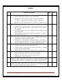
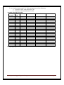
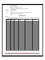
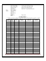
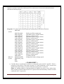
INDEX
Sr.
No.
Name of Experiment
Date
Sign
1 Write a assembly language program to ….
• Add two 8 bit numbers stored in register R6 and R7
• Multiply two 8 bit numbers stored in register R6 and R7.
• To find 1’s complement of number stored in register R0.
•
2
3
4
5
6
To perform AND operation between content of register R0 and
R1.
Write C language program to…
• Read data from port P2 and P3. Add data and display result on
port P0. Glow LED connected at port pinP1.1 if carry flag set
after addition.
• Read data from port P2 and P3. Multiply data and display result
on port P0 and P1.
• Write program to read switch connected at port pin P1.0, toggle it
and send to port pin P1.1.
Write program to…
• To add two sixteen bit numbers stored in DPTR and at memory
location 40h, 41h.Store result in DPTR.
• Multiply two 16 bit numbers. Assume that first 16 bit number is
stored in register R6 and R7, Second 16 bit number is stored in
register R4 and R5. Store answer in register R0,R1,R2 and R3.
Write a program to…
• Add block of data stored at location 40h to 45h.
• Transfer block of data from the location 40h-4Fh to external
memory location 2000h-200Fh.
• Arrange data stored at the location 40h-4Fh in ascending order.
Write a program to perform following…
• Keep monitoring port pin P1.2 until it becomes high.
• When P1.2 becomes high, write data 45h to port P0.
• Send high to low pulse on pin P2.3.
Write a program to generate square wave of 50% duty cycle having
frequency 5 KHz at port pin P1.0 using timer 1 in mode 2. Modify program
to generate pulse waveform of 70% duty cycle using timer on the same pin.
7 Generate external interrupt INT0 and INT1 by connecting push button
switch. Glow LEDs connected at port 1 one by one when interrupt INT0
occurs. LEDs should flash when interrupt INT1 occurs.
BM Dept., Govt. Engg. College, Gandhinagar
Page 3
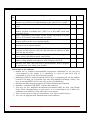
Sr.
No.
8.
9.
10.
11.
12.
13.
14.
15.
16.
17.
Name of Experiment
Date
Sign
Interface seven segment display with Port P2. Write program to display
number 0 to 9 on the seven segment display at the interval of 1 second.
Interface LCD with the microcontroller. Display your name on the
LCD.
Write a program to transmit letter “E” continuously using serial port.
Modify program to transmit text “YES”. Use 8 bit UART mode with
baud rate 19,200.
Write a program to receive bytes of data serially and display it on port
P0. Use 8 bit UART mode with baud rate 9600.
Write a program to count external pulses given at the timer0 input pin.
Display pulses on the seven segment display.
Interface matrix keyboard with 8051. Write program to display key
pressed on seven segment display.
Interface stepper motor with port P0 of the microcontroller. Write a
program to rotate motor in clockwise and anticlockwise direction in half
step and full step mode.
Interface DC motor with 89C51 microcontroller. Write a program to
rotate motor with different speed using PWM.
Interface ADC0808 with 89C51 microcontroller. Write program to read
analog voltage applied at the input of ADC. Display it on LCD.
Interface 8 bit DAC chip with 89C51 microcontroller. Write a program
to generate sine wave using look up table.
Instructions to the students:
• Student has to construct microcontroller mini-project individually as per the given
circuit diagram by the faculty. It is compulsory as a part of term work. List of
components is given at the end of this lab manual.
• Mounting of RS-232 connector and MAX-232 chip is compulsory for all the students
because it will help you to program your chip using Philips Flash Magic Utility (You
have to download HEX files in your chip to test your hardware)
• Simulate assembly language programs on UMPS assembler and simulator.
• Simulate C programs using KEIL compiler and simulator.
• You may use free integrated development environment (IDE) for 8051 with Ubuntu
Linux. Linux operating system is open source so it is convenient to use it. Many free
simulators are available to work with Linux environment.
• Solve exercise given at end of each practical, write answers and execute it.
• Test your all programs with Simulator and actual hardware.
Lab Manual of Microcontroller & Interfacing
Page 4
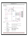
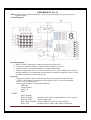
EXPERIMENT NO. 1
AIM: Write a program to ….
• Add two 8 bit numbers stored in register R6 and R7.
• Multiply two 8 bit numbers stored in register R6 and R7.
• To find 1’s complement of number stored in register R0.
• To perform AND operation between content of register R0 and R1.
Assembly language programs:
Program 1: To add two 8 bit numbers stored in register R6 and R7.
ORG 00h
MOV R6,#55h
MOV R7,#44h
MOV A,R6
ADD R7
END
; Transfer data 55h to register R6
; Transfer data 44h to register R7
; Transfer content of register R6 to accumulator
; Add content of R7 with accumulator and store result in A
; End of program
Program 2: To multiply two 8 bit numbers stored in register R6 and R7.
ORG 00h
MOV R6,#55h
MOV R7,#44h
MOV A,R6
MOV B, R7
MUL AB
END
; Transfer data 55h to register R6
; Transfer data 44h to register R7
; Transfer content of register R6 to accumulator
; Transfer content of R7 in register B
; Multiply accumulator and register B, Store result in both
; End of program
Program 3: To find 1’s complement of number stored in register R0. Store result in
register R1.
ORG 00h
MOV A,R0
CPL A
MOV R1,A
END
; Transfer number stored in R0 to Accumulator
; Complement the content of accumulator
; Store result in register R1
; End of program
Program 4: To perform AND operation between content of register R0 and R1. Store
result in register R3.
ORG 00h
MOV A,R0
ANL A,R1
MOV R3,A
END
; Transfer number stored in R0 to Accumulator
; AND operation between A and register R1
; Store result in register R3
; End of program
Note: Check execution of program 3 and 4 by loading different values in registers.
BM Dept., Govt. Engg. College, Gandhinagar
Page 5
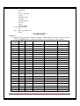
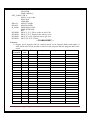
:: WORKSHEET ::
A. Write assembly language program to add two 8 bit data stored at memory locations 60h
and 61h. Store result at location 82h(LSB) and 83h (MSB).
Memory
HEX
Label
Opcode
Operands
Comments
Location
code
B. Write assembly language program to multiply two data stored at memory location 40h
and 41h. Write result of multiplication at memory location 42h (LSB) and 43h (MSB).
Memory
HEX
Label
Opcode
Operands
Comments
Location
code
C. Write and execute instructions to
a. Transfer content 1234h to DPTR.
b. Select register bank 1 and transfer content 45h to register R0 and 54h to R2.
Memory
HEX
Label
Opcode
Operands
Comments
Location
code
Lab Manual of Microcontroller & Interfacing
Page 6
D. Write and execute program to find 2’s complement of number stored in register R0. Store
result in register R1.
Memory
HEX
Label
Location
code
Opcode
Operands
Comments
E. Write and execute program to perform OR operation between data stored at memory
location 40h and 50h. Store result in register R7.
Memory
HEX
Label
Opcode
Operands
Comments
Location
code
BM Dept., Govt. Engg. College, Gandhinagar
Page 7
F. Write and execute program to subtract content of register R6 from register R7 and store
result in register R0.
Memory
HEX
Label
Opcode
Operands
Comments
Location
code
G. Write program to add registers R0,R1 and R2. Consider carry during the addition.
Memory
HEX
Label
Opcode
Operands
Comments
Location
code
H. Write program to add two BCD numbers stored at memory location 50h and 51h. Adjust
result for BCD number and store it at memory location 52h.
Memory
HEX
Label
Opcode
Operands
Comments
Location
code
Lab Manual of Microcontroller & Interfacing
Page 8
:: Rough Work ::
BM Dept., Govt. Engg. College, Gandhinagar
Page 9
EXPERIMENT NO. 2
AIM: Write a C language programs to…
• Read data from port P2 and P3. Add data and display result on port P0. Glow LED
connected at port pinP1.1 if carry flag set after addition.
• Read data from port P2 and P3. Multiply data and display result on port P0 and P1.
• Write program to read switch connected at port pin P1.0, toggle it and send to port pin
P1.1.
C Language Programs:
Program 1: Read data from port P2 and P3. Add data and display result on port P0. Glow
LED connected at port pinP1.1 if carry flag set after addition.
# include <reg51.h>
void main(void)
{
unsigned char a,b,c;
P2=0xff;
//Define port P2 as an input port
P3=0xff;
//Define port P3 as an input port
P0=0x00;
//Define port P0 as an output port
P1=0x00;
//Define port P1 as an output port
P1=0x01;
//Make LED off
a=P2;
//Read port P2
b=P3;
//Read port P3
c=a+b;
//Add content of port P2 and P3
P0 = c;
//Display result on port P0
if(CY==1)
{
P1=0x00;
//Glow LED connected at P1.0 common anode mode
}
}
Program 2: Read data from port P2 and P3. Multiply data and display result on port P0 &
P1.
# include <reg51.h>
void main(void)
{
unsigned char a,b;
unsigned int c;
P2=0xff;
//Define port P2 as an input port
P3=0xff;
// Define port P3 as an input port
P0=0x00;
//Define port P0 as an output port
P1=0x00;
//Define port P1 as an output port
a=P2;
//Read port P2
b=P3;
//Read port P3
c=a*b;
//Multiply content of port P2 and P3
P0 = ACC;
//Display accumulator content on port P0
P1=B;
//Display register B content on port P1
}
Lab Manual of Microcontroller & Interfacing
Page 10
Program 3: Write program to read switch connected at port pin P1.0, toggle it and send it to
port pin P1.1.
# include <reg51.h>
sbit input = P1^0;
/* Define input pin P1.0*/
sbit output=P1^1;
/* Define output pin P1.1*/
void main(void)
{
while(1)
//Continuous infinite loop
{
output=~input;
//Read input pin, toggle it and send to output
}
}
:: WORKSHEET ::
Exercise:
A. Write C language program to continuously toggle pin P1.0 without disturbing other port
pins.
B. Write C language program to perform OR operation between port pin P1.0 and P1.1.
Display result on port pin P1.2.
BM Dept., Govt. Engg. College, Gandhinagar
Page 11
C. Write C language program to read port P1, Compare content of port P1with data 80h. If
data at port P1 is greater than 80h, make port P0=0x00 and if data at port P1 is less than
or equal to 80h, make port P0=0xFF.
D. Write a program to sense lift door switch connected at port pin P2.0. Switch on the alarm
connected at port pin P2.1 if lift door is open. Write program in assembly and C language.
Lab Manual of Microcontroller & Interfacing
Page 12
EXPERIMENT NO. 3
AIM: Write programs to ….
• To add two sixteen bit numbers stored in DPTR and at memory location 40h,41h.Store
result in DPTR.
• Multiply two 16 bit numbers. Assume that first 16 bit number is stored in register R6 and
R7, Second 16 bit number is stored in register R4 and R5. Store answer in register
R0,R1,R2 and R3.Load first value in R6 and R7
Program 1: To add two sixteen bit numbers stored in DPTR and at memory location 40h,
41h. Store result in DPTR.
ORG 00h
MOV DPTR,#2233h
;Transfer 16 bit data to DPTR
MOV 40h,#11h
;Transfer LSB of 16 bit data to location 40h
MOV 41h,#22h
;Transfer MSB of 16 bit data to location 41h
MOV A,40h
; Get LSB of 16 bit data in accumulator
ADD A,DPL
;Add with LSB of second data which is stored in
;DPTR
MOV DPL,A
;Save result back in DPL
MOV A,41h
;Get MSB of first data in accumulator
ADC A,DPH
;Add with MSB of second data consider previous
;carry.
MOV A,DPH
;Save result back in DPH
END
Program 2:
;Load first 16 bit value in R6 and R7
MOV R6,#11h
MOV R7,#22h
;Load second 16 bit value in R4 and R5
MOV R4,#11h
MOV R5,#22h
;Multiply R5 by R7
MOV A,R5
;Move the R5 into the Accumulator
MOV B,R7
;Move R7 into B
MUL AB
;Multiply the two values
MOV R2,B
;Move B (the high-byte) into R2
MOV R3,A
;Move A (the low-byte) into R3
;Multiply R5 by R6
MOV A,R5
;Move R5 back into the Accumulator
MOV B,R6
;Move R6 into B
MUL AB
;Multiply the two values
ADD A,R2
;Add the low-byte into the value already in R2
MOV R2,A
;Move the resulting value back into R2
MOV A,B
;Move the high-byte into the accumulator
BM Dept., Govt. Engg. College, Gandhinagar
Page 13
ADDC A,#00h
MOV R1,A
MOV A,#00h
ADDC A,#00h
MOV R0,A
;Multiply R4 by R7
MOV A,R4
MOV B,R7
MUL AB
ADD A,R2
MOV R2,A
MOV A,B
ADDC A,R1
MOV R1,A
MOV A,#00h
ADDC A,R0
MOV R0,A
;Multiply R4 by R6
MOV A,R4
MOV B,R6
MUL AB
ADD A,R1
MOV R1,A
MOV A,B
ADDC A,R0
MOV R0,A
;Answer is in R0, R1, R2, and R3.
Lab Manual of Microcontroller & Interfacing
;Add zero (plus the carry, if any)
;Move the resulting answer into R1
;Load the accumulator with zero
;Add zero (plus the carry, if any)
;Move the resulting answer to R0.
;Move R4 into the Accumulator
;Move R7 into B
;Multiply the two values
;Add the low-byte into the value already in R2
;Move the resulting value back into R2
;Move the high-byte into the accumulator
;Add the current value of R1 (plus any carry)
;Move the resulting answer into R1.
;Load the accumulator with zero
;Add the current value of R0 (plus any carry)
;Move the resulting answer to R1.
;Move R4 back into the Accumulator
;Move R6 into B
;Multiply the two values
;Add the low-byte into the value already in R1
;Move the resulting value back into R1
;Move the high-byte into the accumulator
;Add it to the value already in R0 (plus any carry)
;Move the resulting answer back to R0
Page 14
:: WORKSHEET ::
Exercise:
A. Write assembly language program to find square of given number stored in register
R0. Save result in register R1 and R2.
Memory
Location
HEX
code
Label
BM Dept., Govt. Engg. College, Gandhinagar
Opcode
Operands
Comments
Page 15
B. Write assembly language program to add 4 digit BCD numbers. First 4 digit number
stored at 40h-41h (LSB at 41h), second 4 digit number stored at location 42h-43h
(LSB at 43h). Store result in DPTR and carry flag.
Memory
Location
HEX
code
Label
Opcode
Lab Manual of Microcontroller & Interfacing
Operands
Comments
Page 16
C. Divide content of register R1 by 8 using logical shift instruction.
Memory
Location
HEX
code
Label
BM Dept., Govt. Engg. College, Gandhinagar
Opcode
Operands
Comments
Page 17
EXPERIMENT NO. 4
AIM: Write a program to ….
• Add block of data stored at location 40h to 45h.
• Transfer block of data from the location 40h-4Fh to external memory location 2000h200Fh.
• Arrange data stored at the location 40h-4Fh in ascending order.
Assembly language programs:
Program 1: Add block of data stored at location 40h to 45h.
In this program, we assume that the result may be 16 bit so it is saved in register
pair A and B with LSB in register A and MSB in register B.
ORG 00h
MOV B,#00h
; Clear B to save the result
MOV R0,#40h
; Use R0 as a pointer to first memory location
MOV A,@R0
; Transfer data from first memory location to accumulator
AGAIN: INC R0
; Point to next memory location
ADD A,@R0
; Add data and store result in accumulator
JNC LOOP
; If no carry do not increment B
INC B
LOOP: CJNE R0,#45h,AGAIN ;Add up to memory location 45h
END
; End of program
Program 2: Transfer block of data from the location 40h-4Fh to external memory location
2000h-200Fh.
ORG 00h
MOV B,#00h
; Clear B to save the result
MOV R0,#40h
; Use R0 as a pointer to first memory location
MOV DPTR,#2000h ; Point to external memory location 2000h
NEXT: MOV A,@R0
; Transfer data from memory to accumulator
MOVX @DPTR,A
; Transfer data from accumulator to external memory
; location pointed by DPTR
INC R0
; Increment R0 to point next location
INC DPTR
; Increment DPTR to point next ext. memory loc.
CJNE R0,#50h,NEXT ;Add up to memory location 4Fh
END
; End of program
Program 3: Arrange data stored at the location 40h-4Fh in ascending order.
ORG 30h
;Start program from the location 30h (why?)
MOV R0,#40h
;Point for first location of data
MOV R1,#40h
loop: MOV b,@R0
start: INC R0
;Point to next data
CLR PSW.7
;Clear carry flag CY before subtraction
MOV A, B
;Transfer data to accumulator for comparison
SUBB A,@R0
;Subtract for comparison
Lab Manual of Microcontroller & Interfacing
Page 18
next:
JC next
MOV 60h,R0
MOV b,@R0
CJNE R0,#4Fh,start
MOV R0,60h
MOV a,@R0
XCH A,@R1
MOV @R0,A
INC R1
MOV A,R1
MOV R0,A
CJNE R1,#4Fh,loop
END
;If A<next data then check next data
;Save smallest location at RAM address 60h
;If A>next data then transfer next data to accumulator
;Check for last location
;Get smallest location again
;Exchange first data with location of smallest no.
;Start search for small number from next location
;Check for last location
:: WORKSHEET ::
Exercise:
A. Write an assembly language program to transfer data from external memory locations
5000h-500Fh to the internal memory locations 30-3Fh.
Memory
Location
HEX
code
Label
BM Dept., Govt. Engg. College, Gandhinagar
Opcode
Operands
Comments
Page 19
B. Write program to arrange data stored in the location 20h-2Fh in descending order.
Memory
Location
HEX
code
Label
Opcode
Lab Manual of Microcontroller & Interfacing
Operands
Comments
Page 20
C. Write program to count number of negative numbers in the array of numbers stored at
external memory location 4000h to 40FFh.
Memory
Location
HEX
code
Label
BM Dept., Govt. Engg. College, Gandhinagar
Opcode
Operands
Comments
Page 21
:: Rough Work ::
Lab Manual of Microcontroller & Interfacing
Page 22
EXPERIMENT NO. 5
AIM: Write a program to ….
• Keep monitoring port pin P1.2 until it becomes high.
• When P1.2 becomes low, write data 45h to port P0.
• Send high to low pulse on pin P2.3.
Program 1: Keep monitoring port pin P1.2 until it becomes high.
ORG 30h
MOV P1,#0FFh
; Configure port P1 as input port
MOV P0,#00h
; Configure port P0 as output port
CLR P2.3
; Make port pin P2.3 low
CHECK: JNB P1.2, CHECK
MOV P0,#45h
CLR P2.3
END
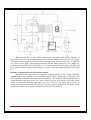
Circuit Diagram:
•
•
•
Construct circuit diagram on general purpose microcontroller board /simulator software.
Assemble and link the program to generate HEX file. Download HEX file into Flash
memory of microcontroller chip 89C51.
Press the reset button and write your comment about which LEDs are ON and OFF.
BM Dept., Govt. Engg. College, Gandhinagar
Page 23
:: WORKSHEET ::
A. Write assembly language and C program to make ALL LEDs connected at port P1 ON.
B. Write assembly language and C program to make ALL LEDs connected at port P1 OFF.
C. Write assembly language and C program to read input switch connected at port pin P3.2
and make all LEDs ON if this switch is pressed and OFF if this switch is released.
Lab Manual of Microcontroller & Interfacing
Page 24
D. A switch is connected to P3.2. Write a program to perform following:
a. If Switch is OFF, send data 0x88 to P0.
b. If Switch is ON, send data 0x55 to P0.
Assembly language program:
Memory
HEX
Label
Opcode
Operands
Comments
Location
code
C language program:
BM Dept., Govt. Engg. College, Gandhinagar
Page 25
EXPERIMENT NO. 6
AIM: Write a program to generate square wave of 50% duty cycle having frequency 5 KHz at
port pin P1.0 using timer 1 in mode 2. Modify program to generate pulse waveform of
70% duty cycle using timer on the same pin.
Calculation of delay:
Time = 1/Frequency = 1/(5x103) = 200 µS
For 50% duty cycle ON time and OFF time are equal
TON = TOFF = 100 µS
Time delay required is 100.
If we consider crystal frequency 12 MHz, time to execute one cycle is
T=
= 1 µS
If we will use pure software delay to generate delay of 100 µS
Program:
ORG 00h
; Start program from location 00h
CLR P1.0
; Make P1.0 output pin
next: ACALL delay
; Call delay of 100 µS
CPL P1.0
; Complement P1.0 to generate square wave
SJMP next
delay: MOV R7,#30h
; Load count value 48 (30h)
loop: DJNZ R7, loop
; Decrement R7 until it becomes zero
NOP
; No operation
RET
; Return to main routine
END
Total number of cycles in delay loop:
Total number if cycles CT = CO + CL + CR = 1 + 4 8⤬2 + 1+2 = 100
Where, CO = Number of cycles outside the loop
CL = Number of cycles inside the loop
CR = Number of cycles for return instruction.
Total time = CT x 1 µS = 100 µS
Note: Execute this program using Keil and observe waveforms at port pin P1.0. (Measure
frequency and verify whether it is giving correct value or not)
:: WORKSHEET ::
Exercise:
A. Modify program for 80% duty cycle.
Hint: Use separate delay loop for ON time and OFF time. Total time is 200 µS, so use
160 µS for ON time and 40 µS for OFF time. You can also prepare delay
subroutine of 10 µS. Call delay subroutine 16 times for ON time and 4 times for
OFF time.
Memory
HEX
Label
Opcode
Operands
Comments
Location
code
Lab Manual of Microcontroller & Interfacing
Page 26
B. Execute following C program in Keil and measure frequency of the square wave.
# include <reg51.h>
sbit wave_pin P1^0;
void sqdelay(unsigned int);
void main(void)
{
while(1)
{
wave_pin=1;
sqdelay(100);
wave_pin=0;
sqdelay(100);
}
}
void sqdelay(unsigned int t)
{
unsigned int i,j;
for(i=0;i<t;i++)
for(j=0;j<1000;j++);
}
Draw waveform (show on time and off time)
BM Dept., Govt. Engg. College, Gandhinagar
Page 27
C. What modifications you suggest in above program to reduce frequency of square wave to
half?
D. Suggest modification in the program to achieve duty cycle 60% without changing
frequency of the square wave.
Lab Manual of Microcontroller & Interfacing
Page 28
EXPERIMENT NO. 7
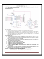
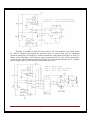
Aim: Generate external interrupt INT0 and INT1 by connecting push button switch. Glow LEDs
connected at port P1 one by one when interrupt INT0 occurs. LEDs should flash when interrupt
INT1 occurs.
Circuit Diagram:
Program:
start:
flash:
org 00h
ajmp start
org 03h
; Vector location for External interrupt INT0
ajmp sequence
; Jump to sequence program
reti
org 13h
; Vector location for External interrupt INT1
ajmp flash
; Jump to flash program
reti
mov IE,#10000101B ;Enable External interrupts
setb IT1
; Negative edge trigger for INT1
setb IT0
; Negative edge trigger for INT0
mov P1,#00h
; Port P1 output port
mov P1,#0ffh
; Make all LEDs OFF
acall delay
mov P1,#00h
; Make all LEDs ON
acall delay
BM Dept., Govt. Engg. College, Gandhinagar
Page 29
ajmp flash
sequence:
mov a,#0FEh
next: mov P1,a
rl a
acall delay
ajmp next
delay: mov R4,#02h
loop3: mov R6,#0ffh
loop2: mov R5,#0ffh
loop1: djnz R5,loop1
djnz R6,loop2
djnz r4,loop3
ret
end
; Bit pattern for First LED ON, others OFF
; Transfer bit pattern to port P1
; Rotate for next LED
; Delay
; Repeat loop
:: WORKSHEET ::
Exercise: Modify program such that when INT0 occurs, LEDs flash ten times and then stop.
When INT1 occurs LEDs glows one by one sequentially only once and then stop.
Hint: Use separate register as a counter.
Memory
HEX
Label
Opcode
Operands
Comments
Location
code
Lab Manual of Microcontroller & Interfacing
Page 30
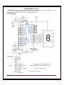
EXPERIMENT NO. 8
Aim: Interface seven segment display with Port P1. Write program to display number 0 to 9 on
the seven segment display. Use delay between two counts.
Program 1: Display Count value on seven segment display.
Circuit diagram:
Program:
again:
ORG 00h
AJMP start
ORG 03h
RETI
start:
MOV P1,#00h
MOV DPTR,#CODE
next: CLR A
MOVC A,@A+DPTR
JZ AGAIN
MOV P1,A
ACALL DELAY
BM Dept., Govt. Engg. College, Gandhinagar
;Configure port 1 as output port
;Initialize DPTR as a base address for code
; Get seven segment code
;Display count value
Page 31
INC DPTR
AJMP next
; Next digit
DELAY: MOV R7,#22h
L3:
MOV R6,#0FFh
L2:
MOV R5,#0FFh
L1:
DJNZ R5,L1
DJNZ R6,L2
DJNZ R7,L3
RET
CODE: db 0C0h,0F9h,0A4h,0B0h,99h,92h,82h,0F8h,80h,90h,00h,
END
Program 2: Interface DIP Switch with port P2 (P2.0 to P2.3). Write a program to read status
of the switch and display its HEX value on the seven segment display connected
at port P1.
Circuit diagram:
Program:
start:
again:
ORG 00h
AJMP start
ORG 03h
RETI
MOV P1,#00h
MOV P2,#0FFh
MOV DPTR,#CODE
MOV A,P2
Lab Manual of Microcontroller & Interfacing
;Configure port 1 as output port
;Configure port 2 as input port
;Initialize DPTR as a base address for code
;Read status of the switch
Page 32
DELAY:
LOOP1:
CODE:
ACALL DELAY
MOVC A,@A+DPTR
MOV P1,A ;Display count value
AJMP again ;Continue DIP switch reading process
MOV R6,#0ffh
DJNZ R6,LOOP1
RET
db 0C0h,0F9h,0A4h,0B0h,99h,92h,82h,0F8h,80h,90h,0C8h,
db 83h,0C6h,0A1h, 86h, 8Eh, 00h
END
:: WORKSHEET ::
Exercise:
A. Write program to display count value F to 0 at the interval of 1 second on seven segment
display connected at port P1.
Memory
HEX
Label
Opcode
Operands
Comments
Location
code
BM Dept., Govt. Engg. College, Gandhinagar
Page 33
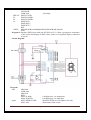
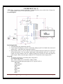
EXPERIMENT NO. 9
AIM: Interface LCD with the microcontroller. Display your name on the LCD.
Interfacing diagram:
Pin connections:
• Data lines of LCD are connected with port P0.
• RS (Register Select) line is connected with port pin P2.0.
• R/W pin is directly connected to ground.
• Enable line is connected with port pin P2.1.
• Relay is driven by transistor SL-100. Transistor SL-100 is controlled by port pin P1.0.
• Push button switches SW1 and SW2 are connected with port Pin P3.2 and P3.3 (External
interrupts pins)
Programming steps:
• Initialize the LCD. For example send command word #38h to initialize LCD for 5⤬7
dots/character and 2 rows. Send command word #3Ch for 5⤬10 dots/character and two
rows. Send other command words like 01h to clear LCD screen, 06h to make LCD ON &
Cursor ON, 80h to start from first line and first character etc.
• Write separate routine to send command in which we will make RS=0 and after
transferring command word to port P1, we will enable LCD by sending pulse at port pin
P3.1. We will use this command routine whenever we want to issue certain commands
during initialization, to clear display, for movement of cursor to display data at particular
position etc.
• Write separate routine to send data to the LCD in which we will make RS=1 and after
transferring data to port P1, we will enable LCD to display data. We will not check
whether LCD is busy or not but we will put certain amount of delay (about 5 ms)
Lab Manual of Microcontroller & Interfacing
Page 34
between two data which gives enough time to LCD for its operation and does not require
to check the status whether it is busy or not.
Program:
; For Kit prepared for LAB
; Program to Display text message on LCD
; Port 1 Drives data lines, P2.1-RS, P2.0 EN,RW is grounded
RS EQU P2.1
RW EQU P2.1
EN EQU P2.0
DATA equ P0
org 00h
MOV P0,#00h
MOV P2,#00h
MOV A,#38h
acall command
MOV A,#0eh
acall command
MOV A,#01h
acall command
MOV A,#06h
acall command
MOV A,#80h
acall command
MOV DPTR,#msg
acall disp_msg
here: sjmp here
command:
acall delay
clr RS
clr RW
mov DATA,A
setb EN
nop
nop
clr EN
ret
disp_data:
acall delay
mov DATA,a
clr RW
setb RS
setb EN
nop
nop
clr EN
ret
disp_msg:
; Port P0 output port
; Port P2 output port
;Initialize LCD, 2 lines, 5X7 matrix
;Issue command to the LCD
;LCD ON, Cursor ON
;Clear LCD
;Shift cursor right
;Force cursor at beginning of the first line
;Point to text message
;Display message on second line
;Write when display not busy
;Select command register
;Set Enable terminal of LCD
;Get data for display
;Select data register
;Enable LCD (Strobe LCD)
;Clear Enable and latch data
BM Dept., Govt. Engg. College, Gandhinagar
Page 35
acall delay
clr a
movc a,@a+dptr
jz exit
acall disp_data
inc dptr
sjmp disp_msg
exit: ret
delay:
mov R6,#0ffh
loop1: djnz R6,loop1
ret
msg: DB ‘ Your name ',0
END
:: WORKSHEET ::
Exercise:
A. Modify LCD program to display two lines: “WELCOME TO B.M.” on first line and
“GEC GANDHINAGAR” on the second line. Execute program in your hardware.
Memory
HEX
Label
Opcode
Operands
Comments
Location
code
Lab Manual of Microcontroller & Interfacing
Page 36
B. Modify program to read status of the switches connected to the port pins P3.2 and P3.3. If
switch SW1 is pressed display “DEVICE ON” and make relay ON. If switch SW2 is
pressed display “DEVICE OFF” and make relay OFF. Execute in your hardware.
Memory
HEX
Label
Opcode
Operands
Comments
Location
code
BM Dept., Govt. Engg. College, Gandhinagar
Page 37
Lab Manual of Microcontroller & Interfacing
Page 38
EXPERIMENT NO. 10
AIM: Write a program to transmit letter “E” continuously using serial port. Modify program to
transmit text “YES”. Use 8 bit UART mode with baud rate 19,200.
Circuit diagram:
Serial data transmission:
Data transmission is unidirectional from microcontroller to the destination device.
Each character takes 33.3 to 0.5 milliseconds for the transmission depending of the baud rate
used. The program must wait until transmission of character is over before loading the next
character in the SBUF. If program does not wait, data will be lost. This can be prevented with
any one of the following method mentioned here.
• Use time delay between transmissions of two characters. Time delay can be chosen
slightly higher than known transmission time of one character. This method is simplest.
• Monitor TI flag of t he SCON special function register (SFR) to check whether character
transmission is completed or not. Next character should be place d only after TI flag is set
i.e. transmission is over.
• TI Flag must be cleared by the program before transmission of next character.
• We can also use interrupt method to check whether transmission is over or not. Serial
interrupt can be invoked by TI or RI flag of SCON special function register. The vector
location for the serial interrupt is 0023h. The serial interrupt bit ES (IE.4) and Enable
interrupts bit EA (IE.7) are set in IE (Interrupt Enable) SFR. When transmission is over,
TI flag will set and serial interrupt will be invoked. Program will jump to the location
0023h where user should writ e a routine to clear TI flag and load S BUF register by new
character. In this practical, we will first write a program using polling method i.e.
continuously checking TI flag and then we will write a program using interrupt method.
Program:
ORG 00H
AJMP START
BM Dept., Govt. Engg. College, Gandhinagar
Page 39
START:
MOV TMOD,#20h
;Configure Timer 1 in mode 2 auto reload mode.
MOV TH1,#0fdh
;Load TH1 with FDh to achieve baud rate 9600
MOV SCON,#50h
;8 bit, 1 stop bit, REN Enabled.
MOV A,PCON
; Transfer content of PCON to accumulator
SETB ACC.7
; Set bit 7 of accumulator
MOV PCON,A
; Set SMOD bit to 1 to double the baud rate
SETB TR1
NEXT:
MOV SBUF,#’E’
;Transfer alphabet ‘A’ to SBUF
HERE:
JNB TI,HERE
;Wait for the last bit
CLR TI
;Clear TI for next ‘A’
SJMP NEXT
END
Modified program:
;Program to transmit text “YES” using Look up table in ROM through
;serial port of the microcontroller using 8 bit UART mode with baud rate
;19,200. TI flag is checked in this program to know whether transmission
;is over or not?
ORG 00H
AJMP START
START:
MOV TMOD,#20h
;Configure Timer 1 in mode 2 auto reload mode.
MOV TH1,#0fdh
;Load TH1 with FDh to achieve baud rate 9600
MOV SCON,#50h
;8 bit, 1 stop bit, REN Enabled.
MOV A,PCON
; Transfer content of PCON to accumulator
SETB ACC.7
; Set bit 7 of accumulator
MOV PCON,A
; Set SMOD bit to 1 to double the baud rate
SETB TR1
REPT:
MOV DPTR,#0400h
NEXT:
CLR A
MOVC A,@A+DPTR
; Get letter from look up table
JZ REPT
MOV SBUF,A
;Transfer letter from look up table
HERE:
JNB TI,HERE
;Wait for the last bit
CLR TI
;Clear TI for next character
INC DPTR
SJMP NEXT
ORG 0400h
DB 'YES',0
EXIT:
END
;Modified program for Serial transmission using interrupt method:
;Program to transmit data from RAM through serial port of
;the microcontroller using 8 bit UART mode with baud rate 9600
;Serial port interrupt is used for data transmission.
ORG 00h
AJMP start
ORG 23h
;Location for serial interrupt
ajmp serial
RETI
;Return from the ISR
start:
Lab Manual of Microcontroller & Interfacing
Page 40
next:
serial:
transmit:
MOV P1,#0ffh
MOV P2,#00h
MOV TMOD,#20h
MOV TH1,#0FDh
MOV SCON,#50h
MOV IE,#90h
MOV R0,#20h
SETB TR1
MOV A,@R0
MOV SBUF,A
INC R0
CJNE R0,#2Fh,next
JB TI, transmit
MOV A, SBUF
MOV P0, A
CLR RI
RETI
CLR TI
RETI
END
;Make P1 output port
;Make P2 output port
;Timer 1, mode-2 ( auto reload mode)
;Count value for baud rate 9600
;8 bit UART mode, REN enable
; Enable serial interrupt and EA bit
;Pointer to the RAM location
;Start timer 1 to generated baud rate.
:: WORKSHEET::
Exercise:
A. Modify program to transmit string “WELCOME TO GEC GANDHINAGAR” using
serial port. Use interrupt method and baud rate 9600.
Memory
HEX
Label
Opcode
Operands
Comments
Location
code
BM Dept., Govt. Engg. College, Gandhinagar
Page 41
B. Write C program to transfer the message “GTU” 255 times serially at 9600 buad, 8-bit
data, 1 stop bit.
Memory
HEX
Label
Opcode
Operands
Comments
Location
code
Lab Manual of Microcontroller & Interfacing
Page 42
BM Dept., Govt. Engg. College, Gandhinagar
Page 43
EXPERIMENT NO. 11
AIM: Write a program to receive bytes of data serially and display it on port P0. Use 8 bit
UART mode with baud rate 9600.
Interfacing diagram:
Pin connections:
• LEDs are connected to port 0 to display received data from the serial port.
• Serial data transfer pins RxD and TxD are connected to the serial port of the computer
thorough IC MAX 232. Max 232 provides necessary voltage conversion from TTL to
serial port standards. As per RS232 standard, logic 1 has voltage range -3 to -25 V and
logic 0 has voltage range +3 to +25 V.
Programming steps:
• The TMOD special function register is loaded with the value 20h to use timer 1 in mode
2 (8 bit auto-reload) to set baud rate. The value FDh is loaded in TH1 register to generate
baud rate 9600 for the crystal of 11.059 MHz.
• The SCON register is loaded with the value 50h, indicating serial mode 1 in which 8 bit
data is framed with start and stop bits.
• The timer 1 run control bit TR1 is set to high.
• The RI flag is cleared with the instruction CLR RI.
• The RI flag is monitored with the instruction:
“CHECK: JNB RI, CHECK” instruction to check whether entire character has been
received or not.
• When reception is over, RI is raised by microcontroller which indicates that SBUF has a
byte and we can read it and display it at LEDs connected at Port P0.
Program 1: Serial data reception using polling method:
ORG 00h
; Start program from memory location 00h
MOV TMOD,#20h ;Timer 1, mode-2 ( auto reload mode)
Lab Manual of Microcontroller & Interfacing
Page 44
MOV TH1,#0FDh
MOV SCON,#50h
MOV P0,#00h
SETB TR1
;Count value for baud rate 9600
;8 bit UART mode, REN enable
;Port P0 output port
;Start timer 1 to generated baud rate.
CHECK:
JNB RI,CHECK
; Check whether data byte is received or not
MOV P0,SBUF
; Display received data on port P0
CLR RI
; Clear RI flag
SJMP CHECK
;Repeat task
END
Program 2: Serial data reception using interrupt method:
In interrupt method, instead of checking RI flag continuously we use serial port
interrupt. When RI flag set, program will automatically jump to the location 0023h which is
vector location of serial interrupt. In this program we read port P1 continuously and display its
content on port P2.
ORG 00h
AJMP start
ORG 23h
;Location for serial interrupt
MOV P0,SBUF
; Display received data on port P0.
start:
CLR RI
RETI
;Return from the ISR
MOV P1,#0ffh
;Make P1 output port
MOV P2,#00h
;Make P2 output port
MOV TMOD,#20h ;Timer 1, mode-2 ( auto reload mode)
MOV TH1,#0FDh ;Count value for baud rate 9600
MOV SCON,#50h ;8 bit UART mode, REN enable
MOV IE,#90h ; Enable serial interrupt and EA bit
SETB TR1 ;Start timer 1 to generated baud rate.
next: MOV A, P1 ; Read port P1
MOV P2,A ; Display content of port P1 on port P2.
SJMP next ;Repeat task
END
Program 3: Program at computer side:
Program for serial communication in “C” language is given here. Alternately we can use
hyper terminal or XTalk software for serial communication.
#include <dos.h>
#include <stdio.h>
#include <conio.h>
#define PORT1 0x3F8
/* Defines Serial Ports Base Address */
/* COM1 0x3F8 COM2 0x2F8 COM3 0x3E8 COM4 0x2E8 */
void main(void)
{
int c,ch;
outportb(PORT1 + 1 , 0);
/* Turn off interrupts - Port1 */
outportb(PORT1 + 0 , 0x0C);
/* Baud rate 9600 */
/* Set Baud rate - Divisor Latch Low Byte */
/* Default 0x03 = 38,400 BPS 0x01 = 115,200 BPS 0x02 = 57,600 BPS
BM Dept., Govt. Engg. College, Gandhinagar
Page 45
/* 0x06 = 19,200 BPS 0x0C = 9,600 BPS 0x18 = 4,800 BPS */
/* 0x30 = 2,400 BPS */
outportb(PORT1 + 1 , 0x00);
/* Set Baud rate - Divisor Latch High Byte
outportb(PORT1 + 3 , 0x03);
/* 8 Bits, No Parity, 1 Stop Bit */
outportb(PORT1 + 2 , 0xC7);
/* FIFO Control Register */
outportb(PORT1 + 4 , 0x0B);
/* Turn on DTR, RTS, and OUT2 */
printf("\nSerial Communication with microcontroller. Press ESC to quit \n");
do { c = inportb(PORT1 + 5);
/* Check to see if char has been received */
if (c & 1) {ch = inportb(PORT1);
/* If so, then get Char */
printf("%c",ch);}
/* Print Char to Screen */
if (kbhit()){ch = getch();
/* If key pressed, get Char */
outportb(PORT1, ch);}
/* Send Char to Serial Port */
} while (ch !=27);
/* Quit when ESC (ASC 27) is pressed */
}
Program 4 : Receive and store data in RAM using interrupt
;Program to receive data through serial port of microcontroller at the
;baud rate 9600. Store data from the RAM location 20h
;This program uses interrupt method for reception of data
start:
ORG 00h
AJMP start
ORG 23h
;Location for serial interrupt
ACALL store
RETI
;Return from the ISR
MOV P1,#0ffh
;Make P1 output port
MOV P2,#00h
;Make P2 output port
MOV TMOD,#20h
;Timer 1, mode-2 ( auto reload mode)
MOV TH1,#0FDh
;Count value for baud rate 9600
MOV SCON,#50h
;8 bit UART mode, REN enable
MOV IE,#90h
; Enable serial interrupt and EA bit
MOV R0,#20h
;Pointer to the RAM location
SETB TR1
;Start timer 1 to generated baud rate.
next:
MOV A, P1
MOV P2,A
SJMP next
;Repeat task
store:
MOV A,SBUF
MOV @R0,A
INC R0
CLR RI
RET
END
Program 5: Receive and store data using polling (status checking)
;Program to receive data through serial port of microcontroller at the
;baud rate 9600. Store data from the RAM location 20h
;This program uses polling method.
ORG 00h
AJMP start
start:
MOV TMOD,#20h
;Timer 1, mode-2 ( auto reload mode)
Lab Manual of Microcontroller & Interfacing
Page 46
next:
HERE:
MOV TH1,#0FDh
MOV SCON,#50h
MOV R0,#20h
SETB TR1
MOV A,SBUF
JNB RI,HERE
CLR RI
MOV @R0,A
INC R0
SJMP next
END
;Count value for baud rate 9600
;8 bit UART mode, REN enable
;Pointer to the RAM location
;Start timer 1 to generated baud rate.
;Repeat task
:: WORKSHEET ::
A. Modify program to display received data on the LCD connected at port P1. Assume
control lines of LCD RS, EN and WR are connected to P2.0, P2.1 and P2.2 respectively.
Memory
HEX
Label
Opcode
Operands
Comments
Location
code
BM Dept., Govt. Engg. College, Gandhinagar
Page 47
:: Rough Work ::
Lab Manual of Microcontroller & Interfacing
Page 48
EXPERIMENT NO. 12
AIM: Write a program to measure frequency of external pulses given at the timer 0 input pin.
Display pulses on the LCD connected at port P1.
Circuit diagram:
Interfacing details:
• LCD data lines are connected to port P1.
• Control lines RS (Register select) is connected with port pin P3.0, Enable line connected
with pin P3.1, read/write line connected with P3.2.
• Opto-coupler PC817 is used to provide optical isolation between signal to be measured
and microcontroller. We can connect input signal with amplitude up to 12V to the optocoupler. We may connect 230V AC signal by using series resistor of 47K at the input of
opto-coupler. Pulses from the opto-coupler PC817 connected to timer input pin T0.
Program:
;To measure frequency of external pulses using 89C51
;LCD Interfacing details:
;Port 1 Drives data lines, P3.0-RS,P3.1 EN,P3.2 RW
;Signal connected through optocoupler PC817 at pin T0 (P3.4)
ORG 00H
AJMP START
ORG 03H
RETI
ORG 0BH
RETI
ORG 13H
RETI
BM Dept., Govt. Engg. College, Gandhinagar
Page 49
ORG 1BH
RETI
ORG 23H
RETI
START:
MOV SP,#60H
MOV P1,#00H
MOV P3,#00h
MOV A,#38H
ACALL COMMAND
MOV A,#0EH
ACALL COMMAND
MOV A,#01H
ACALL COMMAND
MOV A,#06H
ACALL COMMAND
MOV A,#80H
ACALL COMMAND
MOV DPTR,#MSG
ACALL DISP_MSG
MOV TCON,#00H
MOV TMOD,#15H
LOOP:
CHECK:
MOV TL1,#0E0H
MOV TH1,#0B1H
MOV TL0,#00H
MOV TH0,#00H
MOV A,#088H
ACALL COMMAND
MOV R1,#00H
MOV TCON,#50H
JNB TF1,CHECK
CLR TF1
MOV TL1,#0E0H
MOV TH1,#0B1H
SETB TR1
INC R1
CJNE R1,#64H,CHECK
READ_FREQ:
CLR TR0
CLR TR1
MOV 30H,TL0
MOV 31H,TH0
ACALL HEXBCD
Lab Manual of Microcontroller & Interfacing
;Set P1 as an output port
;Set P3 as an output port
;Initialize LCD, 2 lines, 5X7 matrix
;Issue command to the LCD
;LCD ON, Cursor ON
;Clear LCD
;Shift cursor right
;Force cursor at begining of the first line
;Point to message "Freq:"
;Display message on first line
;Timer 0 & Timer 1 off, flags in reset condition
;Timer 1 as a timer in mode 2 &
;Timer 0 as a counter in mode 1.
;Load Timer 1 with 45535(B1E0h)
;results in 0.01 second delay)
;Reset counter for counting operation
;Move cursor to line 2, position 8
;Clear R1 for overflow counting
;Start timer 0 and timer 1
;Load Timer 1 with 45536(b1e0h) results
;in 0.01 SECOND DELAY)
;Count 100 interrupts to provide delay
;100X0.01 =1second
;Stop timer 0
;Stop timer 1
;Transfer LSB of 16 bit count value at RAM
;location30h
;Transfer MSB of 16 bit count value at RAM
;location 31h
;Convert hex number into binary numbers
Page 50
MOV A,37H
ACALL HEXASCI
ACALL DISP_DATA
MOV A,36H
ACALL HEXASCI
ACALL DISP_DATA
MOV A,35H
ACALL HEXASCI
ACALL DISP_DATA
MOV A,34H
ACALL HEXASCI
ACALL DISP_DATA
MOV A,33H
ACALL HEXASCI
ACALL DISP_DATA
AJMP LOOP
;Convert the number stored at 37h into ASCII
; Display ASCII code of number at LCD
HEXASCI:
ADD A,#36H
JNB PSW.6,SKIP
ADD A,#07H
SKIP:
SUBB A,#06H
RET
HEXBCD:
MOV 35h,#0
MOV 36h,#0
MOV 37h,#0
MOV A,30h
MOV B,#10
DIV AB
MOV 33h,B
MOV 34h,A
MOV A,31h
JZ GO_NEXT
MOV B,#10
DIV AB
MOV 35h,B
MOV 36h,A
; Value in 35h is 256 times higher than value standing in 33h, 34h. Mply 35h with 6,
; add to 33h, mply 35h with 5, add to 34h, mply 35h with 2 and replace itself in 35h
MOV R0,#35h
; Point to 35h
ACALL TRANSF
; Transform 35h to 3 lower position
INC R0
; Repeat from 36h, now all registers are 1 higher
ACALL TRANSF
; Transform 36h to 3 higher positions
GO_NEXT:
MOV R0,#33h
; Point to lowest digit i.e. first digit
ACALL DECADJ
RET
TRANSF:
BM Dept., Govt. Engg. College, Gandhinagar
Page 51
MOV A,@R0
MOV B,#6
MUL AB
DEC R0
DEC R0
ADD A,@R0
MOV @R0,A
INC R0
INC R0
MOV A,@R0
MOV B,#5
MUL AB
DEC R0
ADD A,@R0
MOV @R0,A
INC R0
MOV A,@R0
RL A
MOV @R0,A
RET
; Mply with 2
DECADJ:
MOV A,@R0
DECLOP:
MOV B,#10
DIV AB
MOV @R0,B
INC R0
ADD A,@R0
MOV @R0,A
CJNE R0,#37h,DECLOP
RET
COMMAND:
PUSH DPH
PUSH DPL
MOV P1,A
ACALL DELAY
CLR P3.0
CLR P3.2
SETB P3.1
NOP
NOP
CLR P3.1
POP DPL
POP DPH
RET
DISP_DATA:
PUSH DPH
PUSH DPL
Lab Manual of Microcontroller & Interfacing
;Write when when display not busy
;Select command register
;Write Enable
;Set Enable terminal of LCD
Page 52
ACALL DELAY
MOV P1,A
SETB P3.0
CLR P3.2
SETB P3.1
CLR P3.1
POP DPL
POP DPH
RET
;Get data for display
;Select data register
;Enable Write
;Enable LCD (Strobe LCD)
;Clear Enable and latch data
DISP_MSG:
ACALL DELAY
CLR A
MOVC A,@A+DPTR
JZ EXIT
ACALL DISP_DATA
INC DPTR
SJMP DISP_MSG
EXIT:
RET
DELAY:
MOV R7,#22H
LOOP2:
MOV R6,#0FFH
LOOP1:
DJNZ R6,LOOP1
DJNZ R7,LOOP2
RET
MSG:
DB 'FREQ:',0
END
Connect signal from the function generator to the input of opto-coupler and measure frequency
of the signal.
:: WORKSHEET ::
Exercise:
A. Simplify program to count external pulses given at T0 pin. Display this pulses on seven
segment display connected at port P0.
Memory
HEX
Label
Opcode
Operands
Comments
Location
code
BM Dept., Govt. Engg. College, Gandhinagar
Page 53
Lab Manual of Microcontroller & Interfacing
Page 54
EXPERIMENT NO. 13
AIM: Interface matrix keyboard with 8051. Write program to display key pressed on seven
segment display.
Circuit Diagram:
Interfacing details:
• Rows of matrix keyboard are connected to port pins P1.0 to P1.3
• Columns of matrix keyboard are connected to port pins P2.0 to P2.3
• Common anode seven segment display is connected to port P0
• LEDs are connected to port P1.7 to P1.4 and P2.4 to P2.7. These LEDs may be used to
indicate which row is scanned and which column is read by the program. It may be used
to indicate which key is pressed at present.
Program:
; Program to interface matrix keyboard 4x4. Rows are connected to the Port pins
; P1.0-P1.3 & Columns are connected to Port pins P2.0-P2.3. Rows are grounded
; one by one and read columns
; Seven segment display is connected at port P0
ORG 00h
AJMP START
ORG 13h
RETI
START:
MOV P0,#00h
MOV P2,#0FH
; Port Pins P2.0 to P2.3 i/p pins and P2.4 to P2.7 o/p pins
MOV P1,#00H
;Port P0 output port
REL: MOV P1,#00H ; Make All Rows Ground To Check All Keys
MOV A,P2
;Read Port P2 To Ensure That All Keys Released
BM Dept., Govt. Engg. College, Gandhinagar
Page 55
ANL A,#0FH
;Maks Upper Bits Because They Are Not Used
CJNE A,#0FH,REL ;Check Till All Keys Released
AGAIN:
ACALL DELAY
MOV A,P2
;See If Any Key Pressed Or Not?
ANL A,#0FH
;Mask Upper Bits
CJNE A,#0FH,KPRESS ; If A Is Not Equal To 0fh Then Key Is
; Pressed
SJMP AGAIN
; Check Again If Key Is Not Pressed
KPRESS:
ACALL DELAY
MOV A,P2
ANL A,#0FH
;MASK UNUSED UPPER BITS
CJNE A,#0FH,KPRESS1 ; if a is not equal to 0fh then key is
;pressed
SJMP AGAIN
; CHECK AGAIN IF KEY IS NOT PRESSED
KPRESS1:
MOV P1,#0FEH
MOV A,P2
ANL A,#0FH
CJNE A,0FH,R_0
MOV P1,#0FDH
MOV A,P2
ANL A,#0FH
CJNE A,0FH,R_1
MOV P1,#0FBH
MOV A,P2
ANL A,#0FH
CJNE A,0FH,R_2
MOV P1,#0F7H
MOV A,P2
ANL A,#0FH
CJNE A,0FH,R_3
R_0:
R_1:
R_2:
R_3:
CHECK_C:
; Ground ROW 0
;Read All Columns
;Mask Unused Upper Bits
;key is pressed in first row (row 0),check
; columns
; Ground ROW 1
;READ ALL COLUMNS
;MASK UNUSED UPPER BITS
;KEY IS PRESSED IN SECOND ROW (ROW 1),CHECK
; COLUMNS
; Ground ROW 2
;READ ALL COLUMNS
;MASK UNUSED UPPER BITS
;KEY IS PRESSED IN THIRD ROW (ROW 2),CHECK
; COLUMNS
; Ground ROW 0
;READ ALL COLUMNS
;MASK UNUSED UPPER BITS
;KEY IS PRESSED IN FOURTH ROW (ROW 3),CHECK
; COLUMNS
LJMP AGAIN
MOV DPTR,#KCODE0 ;SET DPTR=START OF ROW 0
SJMP CHECK_C
MOV DPTR,#KCODE1 ;SET DPTR=START OF ROW 1
SJMP CHECK_C
MOV DPTR,#KCODE2 ;SET DPTR=START OF ROW 2
SJMP CHECK_C
MOV DPTR,#KCODE3 ;SET DPTR=START OF ROW 3
RRC A
JNC GET_CODE
;CHECK WHETHER CARRY OCCURS OR NOT
Lab Manual of Microcontroller & Interfacing
Page 56
INC DPTR
SJMP CHECK_C
GET_CODE: CLR A
MOVC A,@A+dptr
MOV P0,A
LJMP REL
DELAY:
MOV R7,#0FFh
DLOOP:
MOV R6,#0FFh
D_LOOP: DJNZ R6,D_LOOP
DJNZ R7,DLOOP
RET
KCODE0: DB '0','1','2','3' ;These codes are for LCDs
KCODE1: DB '4','5','6','7' ;Replace this code by seven
KCODE2: DB '8','9','A','B' ;segment code as per your
KCODE3: DB 'C','D','E','F' ;Circuit.
:: WORKSHEET ::
Exercise:
A. Prepare seven segment code for common anode seven segment display and replace it
with ASCII code in look up table as shown in the program. Run the program and see the
result.
Memory
HEX
Label
Opcode
Operands
Comments
Location
code
BM Dept., Govt. Engg. College, Gandhinagar
Page 57
B. Modify program such that LEDs connected at P1.4 to P1.7 shows which row is scanned
by the program and P2.4 to P2.7 shows which key is pressed in each row.
Memory
HEX
Label
Opcode
Operands
Comments
Location
code
Lab Manual of Microcontroller & Interfacing
Page 58
:: Rough Work ::
BM Dept., Govt. Engg. College, Gandhinagar
Page 59
EXPERIMENT NO. 14
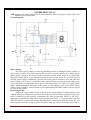
AIM: Interface stepper motor with port P0 of the microcontroller. Write a program to rotate
motor in clockwise and anticlockwise direction in half step and full step mode.
Circuit diagram:
Interfacing details:
Interfacing of small torque stepper motor with torque of 2Kg-cm is shown in above
diagram. Such motor requires current rating of 0.5 A per phase. Four terminals of the stepper
motor are controlled with PORT P0. As PORT P0 cannot supply desired current, IC ULN 2803
is used to supply necessary drive current to the motor. ULN2803 is high voltage high current
Darlington arrays consists of eight Darlington open collector transistors. Each Darlington pair
can drive load current upto 500 mA. This IC consists of internal suppression diodes for the
inductive loads. These diodes are used to protect switching transistor from breakdown. When
transistor switched from ON to OFF state, large voltage induced across coil of stepper motor can
damage the transistor. The suppression diode discharge energy stored in the inductor when
transistor is in OFF condition.
To drive stepper motor with torque 7 kg-cm, +12V it requires current of 2A/phase. This
stepper motor requires combination of transistor SL-100 and 2N3055 as shown in the following
circuit diagram. Program will remain same. Control signals may come from any port of
microcontroller. In this circuit control signals from port pins P1.0 to P1.3 are shown.
Lab Manual of Microcontroller & Interfacing
Page 60
Sequence of pulses required to send on port P0 to rotate motor in clockwise and anticlockwise
direction for full step mode:
Program 1: To rotate motor for 100 steps in clockwise direction (Full step)
ORG 30h
MOV P0,#00h
;Configure port P0 as an output port
MOV R0, #64h
;Load count value for 100 steps
MOV A,#11h
;Load accumulator with 11h
loop:
MOV P0,A
;Sent data to port 1 (stepper motor)
delay:
ACALL delay
;Delay to control speed
RL A
;Next data
DJNZ R0, loop
;Continue rotation if no. of steps<100
MOV R2,#0FFh
;Change this count to change speed
d_loop:
DJNZ R2,d_loop
RET
END
BM Dept., Govt. Engg. College, Gandhinagar
Page 61
Sequence of pulses required to send on port P0 to rotate motor in clockwise and anticlockwise
direction for half step mode:
Program 2: To rotate motor in half step mode continuously in clockwise direction.
ORG 40h
LOOP:
MOV P0,,#00h
;Define port P0 as output port
MOV P0,#01h
;Sent data to port 1 (stepper motor)
CALL DELAY
;Delay to control speed
MOV P0,#03h
;Sent data to port 1 (stepper motor)
CALL DELAY
;Delay to control speed
MOV P0,#02h
;Sent data to port 1 (stepper motor)
CALL DELAY
;Delay to control speed
MOV P0,#06h
;Sent data to port 1 (stepper motor)
CALL DELAY
;Delay to control speed
MOV P0,#04h
;Sent data to port 1 (stepper motor)
CALL DELAY
;Delay to control speed
MOV P0,#0Ch
;Sent data to port 1 (stepper motor)
CALL DELAY
;Delay to control speed
MOV P0,#08h
;Sent data to port 1 (stepper motor)
CALL DELAY
;Delay to control speed
MOV P0,#09h
;Sent data to port 1 (stepper motor)
CALL DELAY
;Delay to control speed
JMP LOOP
;Continue rotation
DELAY:
MOV R2,#0FFh
;Change this count to change speed
d_loop:
DJNZ R2,d_loop
RET
END
:: WORKSHEET ::
A. Consider that two push-button switches are connected at port pins P3.2 and P3.3. Write a
program so that speed of the motor increases if switch connected at P3.2 pressed and
speed of the motor reduces if switch connected at port pin P3.3 is pressed.
(Hint: use polling method or interrupt method to monitor key press event, reduce timer
delay counter if switch connected at P3.2 is pressed. Increase time delay counter if switch
connected at P3.3 is pressed)
Lab Manual of Microcontroller & Interfacing
Page 62
Memory
Location
HEX
code
Label
BM Dept., Govt. Engg. College, Gandhinagar
Opcode
Operands
Comments
Page 63
B. Consider that switch SW1 and SW2 shown in the circuit are two limit switches are
connected at external interrupt pins P3.2 and P3.3. Write a program so that when switch
SW1 is pressed, stepper motor rotates clockwise and when switch SW2 pressed, stepper
motor rotates anticlockwise.
(Hint: Use external interrupt vector location. Prepare clockwise routine and call it at
location 03h. Prepare anticlockwise routine and call it at vector location 13h. Enable
external interrupt bits in IE SFR)
Memory
HEX
Label
Opcode
Operands
Comments
Location
code
Lab Manual of Microcontroller & Interfacing
Page 64
EXPERIMENT NO. 15
AIM: Interface DC motor with AT89C51 microcontroller. Write a program to rotate motor with
different speed using PWM.
Circuit Diagram:
Basic concept:
DC motor speed control is useful in controlling motion in industrial control systems as
well as arm of robots. To control speed of DC motor, we can use variable DC voltage source.
When supply is given to DC motor, it takes some time to reach at full speed. If we switch OFF
DC power supply before it gets maximum speed, it starts to slow down. If we switch ON and
OFF DC power supply continuously, speed of DC motor will be in between zero and full rated
speed. If duty cycle is more (i.e. ON time is more than OFF time) speed is more and if duty cycle
is less (ON time is less than OFF time), speed of the motor is also less. Thus, if we apply PWM
(Pulse Width Modulated) waveform to the motor, we can change speed of the motor. When
width of pulse is highest, speed of motor is also highest and when width of pulse is lowest, speed
of motor is also lowest.
Interfacing details:
Simple DC motor control circuit is shown in the circuit diagram. Common anode seven
segment display is connected to port P0 to show the speed of the motor in numeric form. DC
motor is connected to the collector of transistor (We can use transistor TIP122 or 2N 3055).
Transistor is controlled by signal from microcontroller port pin P1.1. Two push button switches
SW1 and SW2 are connected at external interrupt pins to control speed of the DC motor. We can
write program such that width of pulses increases when we press switch SW1 and width of
BM Dept., Govt. Engg. College, Gandhinagar
Page 65
pulses decreases when we press the switch SW2. This will control speed of the motor. Transistor
acts as a switch which becomes ON when port pin P1.1 is set and becomes OFF when port pin
P1.1 is reset.
Program:
ORG 00h
SJMP START
ORG 03h
INC B
; Increase R7 to increase width of pulse
RETI
ORG 13h
DEC B
;Decrease R7 to decrease width of pulse
RETI
START:
MOV IE,#85h
; Enable external interrupt 0 and 1
SETB IT0
; Negative edge triggered interrupt
SETB IT1
;Negative edge triggered interrupt
CLR P1.1
; Make P1.1 output pin
MOV B,#80h
; Initial speed
next:
SETB P1.0
ACALL ON_delay ; Call delay for ON time
CLR P1.0
; Complement P1.0 to generate square wave
ACALL OFF_delay ; Call delay for OFF time
SJMP next
OFF_delay:
MOV R4,#00h
L1:
DJNZ R4, L1
RET
ON_delay:
MOV R7,B
; Load count value from register B
L3:
MOV R6,#0FFh
L2:
DJNZ R6, L2
; Decrement R6 until it becomes zero
DJNZ R7,L3
NOP
; No operation
RET
; Return to main routine
END
Optical isolation:
It is better to use opto-isolator between motor circuit and microcontroller because it will
protect microcontroller from EMI created by the motor brushes. If motor voltage rating is higher
than the voltage used for microcontroller then opto-isolator prevents damage to the
microcontroller by providing optical isolation. If there is any fault in motor circuit or power
supply, microcontroller is safe. Modified circuit using optoisolator is shown below:
Lab Manual of Microcontroller & Interfacing
Page 66
When port pin P1.1 is low, LED of opto-isolator will glow which makes transistor of
opto-isolator ON. Current flows through base of transistor TIP120 and motor gets DC supply.
Transistor of opto-isolator and TIP120 forms Darlington pair. When port pin P1.1 is high (i.e.
set), LED will not glow, both transistors remains off and motor will not get DC supply. By
controlling ON and OFF time of the LED, we can control speed of the DC motor. Program will
be very much similar to the previous program, except we will interchange SETB P1.1 and CLR
P1.1.
H-Bridge configuration for bi-directional rotation:
Direction of DC motor can be changed by changing polarity of DC voltage. H-Bridge
configuration is very popular for bi-directional speed control. Interfacing of H-bridge with
microcontroller is shown in the following circuit diagram. We need four microcontroller pins to
control direction and speed of the DC motor. When port pins P1.0 and P1.4 are high, motor
rotates in clockwise direction and when pins P1.1 and P1.2 are high; motor rotates in
anticlockwise direction because of reversal in current. Optical isolation is not shown in the
circuit but it is better to use optical isolation for safety of microcontroller.
BM Dept., Govt. Engg. College, Gandhinagar
Page 67
H-bridge is available in single IC form such as L293. Four transistors are inbuilt in this
IC. This IC produces heat during the operation, hence it requires heat sink for continuous
operation. Interfacing of H-bridge IC with microcontroller using Quad optocoupler IC ILQ74 is
shown in the following Circuit diagram. Quad optocoupler IC has four in-built optocoupler
which provides optical isolation between H-bridge circuit and microcontroller 89C51. Separate
power supply can be used for microcontroller and motor circuit.
Lab Manual of Microcontroller & Interfacing
Page 68
Program: Write a program to rotate DC motor connected in above circuit such that when switch
SW1 is pressed, motor rotates in clockwise direction and when SW2 is pressed, motor rotates in
anti-clockwise direction. Use external interrupts for the program.
ORG 00h
AJMP START
ORG 03h
; Vector location for external interrupt 0
SETB P1.1
; Rotate motor in clockwise direction
CLR P1.0
; -- do -RETI
ORG 13h
; Vector location for external interrupt 1
SETB P1.1
; Rotate motor in anticlockwise direction
CLR P1.0
; -- do -RETI
START:
CLR P1.0
; Make P1.0 output pin
CLR P1.1
; Make P1.1 output pin
CLR P1.2
; Make P1.2 output pin
MOV IE,#85h
; Enable external interrupt 0 and 1
SETB IT0
; Negative edge triggered interrupt
SETB IT1
; Negative edge triggered interrupt
SETB P1.0
; Enable chip L293 (H-bridge)
HERE:
SJMP HERE
:: WORKSHEET ::
A. Modify previous program without using interrupts.
(Hint: using polling method to check whether switch is pressed or not like JNB P3.2,
clockwise.)
Memory
HEX
Label
Opcode
Operands
Comments
Location
code
BM Dept., Govt. Engg. College, Gandhinagar
Page 69
B. Modify the first program of this practical, so that speed of the DC motor displayed on the
seven segment display.
(Hint: Use look up table method to display 0 for minimum speed and 9 to display
maximum speed.)
Memory
HEX
Label
Opcode
Operands
Comments
Location
code
Lab Manual of Microcontroller & Interfacing
Page 70
:: Rough Work ::
BM Dept., Govt. Engg. College, Gandhinagar
Page 71
EXPERIMENT NO. 16
AIM: Interface ADC0808 with AT89C51 microcontroller. Write a program to read analog
voltage applied at the input of ADC. Display hex code of analog value on LEDs connected
at port P0.
Circuit diagram:
Program:
; Microcontroller connections to ADC0808/9 lines.
START
EQU P3.6
; Pin 6 Start
EOC
EQU P3.2
; Pin 7 EOC
OE
EQU P3.7
; Pin 9 Output Enable
ALE
EQU P3.6
; Pin 22 ALE
LOOP:
ORG 00h
MOV P0,#00h
MOV P1,#0FFH
MOV P2,#00H
MOV R0,#05H
MOV P0,#0FFH
ACALL DELAY
MOV P0,#00H
ACALL DELAY
DJNZ R0,LOOP
; P0 OUTPUT PORT TO DRIVE LEDs
; P1 INPUT PORT TO READ ADC
; P2 OUTPUT PORT TO SELECT CHANNEL
BACK:
MOV P2,#00H
ACALL SDELAY
; SELECT ADC CHANNEL 0
Lab Manual of Microcontroller & Interfacing
Page 72
HERE:
HERE1:
DELAY:
L3:
L2:
L1:
SETB EOC
CLR ALE
CLR OE CLR
START SETB
START ACALL
SDELAY CLR
START
JB EOC,HERE
JNB EOC,HERE1
SETB OE
ACALL SDELAY
MOV A,P1
CPL A
MOV P0,A
CLR OE
AJMP BACK
MOV R7,#02h
MOV R6,#00h
MOV R5,#00h
DJNZ R5,L1
DJNZ R6,L2
DJNZ R7,L3
RET
; MAKE EOC INPUT
SDELAY:
SL2:
SL1:
MOV R6,#00h
MOV R5,#00h
DJNZ R5,SL1
DJNZ R6,SL2
RET
END
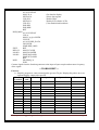
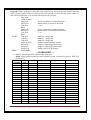
Observations:
Input
Voltage
D7
0.5 V
1V
2V
2.5 V
3V
4V
5V
D6
LED Status (ON/OFF)
D5
D4
D3
D2
BM Dept., Govt. Engg. College, Gandhinagar
D1
D0
Hex
Value
Page 73
:: WORKSHEET::
A. Write a program to read analog value at the interval of 1 second and store it at memory
location 50h onwards. Store total 16 values.
Memory
HEX
Label
Opcode
Operands
Comments
Location
code
Lab Manual of Microcontroller & Interfacing
Page 74
B. Draw interfacing diagram to interface ADC0804 with AT89C51 microcontroller. Write
program to read analog data and display its digital value on seven segment display
connected at port P0.
Memory
Location
HEX
code
Label
BM Dept., Govt. Engg. College, Gandhinagar
Opcode
Operands
Comments
Page 75
:: Roght Work ::
Lab Manual of Microcontroller & Interfacing
Page 76
EXPERIMENT NO. 17
AIM: Interface 8 bit DAC chip with 89C51 microcontroller. Write a program to generate sine
wave using look up table.
Circuit diagram:
Interfacing details:
• Data lines of DAC-0808 are connected with Port P1 of the microcontroller AT89C51.
• Zener diode is used to provide reference voltage to the DAC.
• Current output of the DAC is converted into voltage by I to V converter circuit formed by
Op-AMP 741.
• Connect C.R.O. at the output of DAC to observe analog signal.
Program:
org 30h
rept:
mov dptr,#0400h
mov P1,#00h
start:
clr a
movc a,@a+dptr
jz rept
add a,#127
mov P1,a
setb P0.7
acall delay
inc dptr
ajmp start
delay:
mov R7,#0ffh
loop:
djnz R7,loop
ret
BM Dept., Govt. Engg. College, Gandhinagar
Page 77
org 0400h
DB 1,8,16,24,32,40,47,54,62,69,75,82,88,93,99,104,108,112,116,119,122,124,124
DB 126,127,127,127,126,124,124,122,119,116,112,108,104,99,93,88,82,75,69,62,54
DB 47,40,32,24,16,8,1,-8,-16,-24,-32,-40,-47,-54,-62,-69,-75,-82,-88,-93,-99,-104
DB -108,-112,-116,-119,-122,-123,-124,-125,-126,-127,-127,-127,-126,-124,-122,-119
DB -116,-112,-108,-104,-99,-93,-88,-82,-75,-69,-62,-54,-47,-40,-32,-24,-16,-8,1,0
end
:: WORKSHEET::
Exercise:
A. Modify DAC program to generate ramp waveform at the output.
Memory
HEX
Label
Opcode
Operands
Location
code
Lab Manual of Microcontroller & Interfacing
Comments
Page 78
B. Modify DAC program to generate Full wave rectifier waveform at the output.
Memory
HEX
Label
Opcode
Operands
Comments
Location
code
BM Dept., Govt. Engg. College, Gandhinagar
Page 79
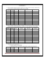
Component list for microcontroller mini-project and practical:
Part 1: List of components compulsory for all the students
1. Microcontroller IC Phillips 89V51RD2 with socket
2. Crystal 11.059 MHz
3. IC Max232 with socket
4. Male female connectors strip (According to PCB)
5. Capacitors:
a. 33pF
---- 2
b. 1000µF, 25V
---- 1
c. 10µF, 25V
---- 6
---- 1
d. 100µF, 25V
6. Resistors
a. 10K
---- 12
b. 470Ω
---- 8
c. 1 K
---- 8
d. 100 Ω
---- 2
e. RN10K
---- 2
(Resistor network, eight resistors in array, 10K Ω)
7. Transistor SL-100
---- 1
8. Tactile push-button switch
---- 9
9. LED (Red and Green) ---- 4 each
10. General purpose microcontroller PCB
11. Serial cable
12. DC power supply socket (Female)
13. IC LM7805
14. Bridge rectifier 1 A
15. Transformer 0-12V
(Student can purchase +5V DC adapter (charger) instead of item no. 13 to 15)
Part 2: Components as per group:
Group 1:
1. LCD Module 16 character*2 line (With socket) and necessary connectors.
2. 10K preset
Group 2:
1. Common anode seven segment display
--- 2
--- 2
2. Resistors 680Ω
Group 3:
1. IC L293D
2. Small DC motor
3. ILQ 74 opto-isolator
Group 4:
1. DIP Switch (array of 4 switch)
--- 2
Group 5:
1. Matrix keyboard
2. Common anode seven segment display
Group 6:
1. Relay 12V, 100 Ω (PCB mounted), Bulb holder
Group 7:
1. PC817 opto-coupler and LCD module with socket
Group 8:
1. Small stepper motor
2. IC ULN 2803
Group 9:
1. Thumb wheel switch, Common anode seven segment display and PCB mounted relay
Group 10:
1. DAC 0808,
2. Op-amp 741 (with socket),
3. Zener diode 10V,
4. Resistors 5.1K --- 2,
5. Capacitors 0.01µF and 0.1 µF
Group 11:
1. ADC0808 (with socket),
2. IC CD4024 with socket,
3. POT 10K.
Lab Manual of Microcontroller & Interfacing
Page 80