1
Intel® SRMK2 Internet Server
Technical Product Specification
February 26, 2001
iPN A39185-001
The Intel ® SRMK2 Internet Server may contain design defects or errors known as errata which may cause the product to deviate from published specifications. Current characterized errata are documented in the
Intel® SRMK2 Internet Server Specification Update.
Revision History
Revision
Revision History
Date
1.0
Original draft
October 18, 2000
1.1
First update
January 25, 2001
1.2
Second update
February 26, 2001
Information in this document is provided in connection with Intel products. No license, express or implied, by estoppel or
otherwise, to any intellectual property rights is granted by this document. Except as provided in Intel's Terms and Conditions of
Sale for such products, Intel assumes no liability whatsoever, and Intel disclaims any express or implied warranty, relating to sale
and/or use of Intel products including liability or warranties relating to fitness for a particular purpose, merchantability, or
infringement of any patent, copyright or other intellectual property right. Intel products are not intended for use in medical, life
saving, or life sustaining applications.
Intel retains the right to make changes to specifications and product descriptions at any time, without notice.
The Intel® SRMK2 Internet Server may contain design defects or errors known as errata that may cause the product to deviate
from published specifications. Current characterized errata are available on request.
Contact your local Intel sales office or your distributor to obtain the latest specifications before placing your product order.
Copies of documents which have an ordering number and are referenced in this document, or other Intel literature, may be
obtained from:
Intel Corporation
P.O. Box 5937
Denver, CO 80217-9808
or call in North America 1-800-548-4725, Europe 44-0-1793-431-155, France 44-0-1793-421-777,
Germany 44-0-1793-421-333, other Countries 708-296-9333.
† Third-party brands and names are the property of their respective owners.
Copyright 2000, Intel Corporation. All rights reserved.
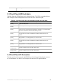
Preface
This Technical Product Specification (TPS) identifies components and software integrated with
the Intel® SRMK2 Internet Server. These components include the serverboard, riser card, front
panel board, hot-swap backplane, system BIOS, Advanced Server Management (ASM) software,
chassis, and power supply. Certifications, reliability, and serviceability of the system are also
discussed.
Intended Audience
This TPS provides detailed technical information about the SRMK2 Internet Server and its internal
components. This information is intended for xSPs, OEM engineers, vendors, system integrators,
and other engineers and technicians who need this level of information. It is not intended for
general audiences.
Typographical Conventions
This section describes the conventions used in this specification. Not all of these symbols and
abbreviations appear in all specifications of this type.
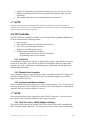
!
NOTE
Notes call attention to important information.
CAUTION
Cautions are included to help you avoid damaging hardware and losing data.
WARNING
Warnings indicate conditions that, if not observed, can cause personal injury.
Intel® SRMK2 Internet Server Technical Product Specification
iii
<Blank Page: Prevention words>
Intel® SRMK2 Internet Server Technical Product Specification
iv
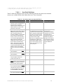
Conventions and Terminology
Contents
1
INTRODUCTION...............................................................................................................................................11
2
CHASSIS DESCRIPTION ...............................................................................................................................13
2.1
EXTERNAL CHASSIS FEATURES.............................................................................................................. 13
2.1.1
Chassis Dimensions................................................................................................................................ 13
2.1.2
Colors of Chassis.................................................................................................................................... 13
2.1.3
Front View of Chassis ............................................................................................................................. 14
2.1.4
Rear View of Chassis .............................................................................................................................. 15
2.2
INTERNAL CHASSIS FEATURES............................................................................................................... 15
2.2.1
AC Power Supply .................................................................................................................................... 15
2.2.2
DC Power Supply.................................................................................................................................... 19
2.2.3
BTU information..................................................................................................................................... 19
2.2.4
System Cooling........................................................................................................................................ 20
2.2.5
System Peripheral Bays........................................................................................................................... 21
2.2.6
System Interconnection............................................................................................................................ 21
2.3
SYSTEM CONFIGURATION ...................................................................................................................... 23
3
SRMK2 SERVERBOARD DESCRIPTION ..................................................................................................24
3.1
OVERVIEW ................................................................................................................................................. 24
3.2
SERVERBOARD LAYOUT .......................................................................................................................... 25
3.3
PROCESSORS............................................................................................................................................... 27
3.4
CHIPSET ..................................................................................................................................................... 28
3.4.1
ServerWorks CNB30LE North Bridge Chip........................................................................................... 28
3.4.2
ServerWorks OSB4 South Bridge Chip .................................................................................................. 29
3.5
M EMORY.................................................................................................................................................... 30
3.6
SCSI HOST BUS INTERFACE .................................................................................................................... 31
3.6.1
SCSI Hard Drive LED Connector (Optional) ........................................................................................ 31
3.7
IDE INTERFACE ......................................................................................................................................... 31
3.8
USB............................................................................................................................................................. 31
3.9
I/O CONTROLLER ..................................................................................................................................... 32
3.9.1
Serial Port............................................................................................................................................... 32
3.9.2
Diskette Drive Controller ....................................................................................................................... 32
3.9.3
Keyboard and Mouse Interface............................................................................................................... 32
3.9.4
Real-Time Clock, CMOS SRAM, and Battery......................................................................................... 32
3.10
INTEL ® 82559 10/100 ETHERNET CONTROLLERS................................................................................ 33
3.11
VIDEO INTERFACE .................................................................................................................................... 33
3.12
HARDWARE M ONITOR ............................................................................................................................ 34
3.13
W AKE ON RING AND RESUME ON RING ............................................................................................... 35
3.13.1
Wake on Ring..................................................................................................................................... 35
3.13.2
Resume on Ring.................................................................................................................................. 35
3.14
SPEAKER.................................................................................................................................................... 35
3.15
FAN SUPPORT ........................................................................................................................................... 36
3.16
BASEBOARD PROGRAMMING .................................................................................................................. 36
3.16.1
PCI Configuration Space Map........................................................................................................... 36
3.16.2
Interrupts ........................................................................................................................................... 36
3.16.3
SMI and NMI Routing........................................................................................................................ 37
3.16.4
System Management Bus (SMB) ........................................................................................................ 37
3.17
BASEBOARD CONNECTORS AND JUMPERS........................................................................................... 38
Intel® SRMK2 Internet Server Technical Product Specification
v
Conventions and Terminology
3.17.1
Back Panel I/O Connectors................................................................................................................ 39
3.17.2
Midboard Connectors........................................................................................................................ 41
3.17.3
Front Panel Connector....................................................................................................................... 48
3.18
JUMPER BLOCKS....................................................................................................................................... 50
3.19
THERMAL CONSIDERATIONS.................................................................................................................. 52
3.20
DC VOLTAGE REGULATION ................................................................................................................... 53
4
PCI RISER BOARD ..........................................................................................................................................54
4.1
4.2
4.3
4.4
5
FRONT PANEL BOARD..................................................................................................................................57
5.1
5.2
5.3
5.4
6
INTRODUCTION ........................................................................................................................................ 57
FRONT PANEL SWITCHES....................................................................................................................... 57
FRONT PANEL LED INDICATORS........................................................................................................... 58
FRONT PANEL I/O CONNECTOR ............................................................................................................ 58
SCSI BACKPLANE...........................................................................................................................................59
6.1
7
INTRODUCTION ........................................................................................................................................ 54
RISER BOARD PCI BUS CONNECTORS.................................................................................................... 54
PCI A DD-IN CARDS................................................................................................................................... 54
RISER BOARD PCI INTERRUPT ROUTING M AP ................................................................................... 55
INTRODUCTION ........................................................................................................................................ 59
BIOS DESCRIPTION .......................................................................................................................................61
7.1
OVERVIEW ................................................................................................................................................. 61
7.2
SYSTEM BIOS............................................................................................................................................ 61
7.2.1
Configuration Utility ............................................................................................................................... 62
7.2.2
CMOS Configuration RAM Summary..................................................................................................... 62
7.2.3
Flash Memory Update Utility.................................................................................................................. 62
7.2.4
Fail-Safe BIOS Extensions ...................................................................................................................... 62
7.2.5
System Flash ROM Layout...................................................................................................................... 62
7.3
SYSTEM BIOS............................................................................................................................................ 63
7.3.1
Auto-Configuration Features .................................................................................................................. 63
7.3.2
Performance Features............................................................................................................................. 67
7.3.3
Reliability Features.................................................................................................................................. 69
7.3.4
System Services ....................................................................................................................................... 71
7.3.5
Boot Options ........................................................................................................................................... 74
7.3.6
OEM Customization................................................................................................................................ 75
7.3.7
SMBIOS Support..................................................................................................................................... 78
7.3.8
Soft Power Switch.................................................................................................................................... 79
7.3.9
POST Memory Manager Support........................................................................................................... 80
7.3.10
ACPI Support..................................................................................................................................... 80
7.4
FAIL-SAFE BIOS EXTENSIONS................................................................................................................ 81
7.4.1
LAN Alerts............................................................................................................................................... 81
7.4.2
WatchDog Timer (WDT) ........................................................................................................................ 81
7.4.3
Paging Support....................................................................................................................................... 82
8
FLASH MEMORY UPDATE UTILITY...........................................................................................................83
8.1
9
LOADING THE SYSTEM BIOS ................................................................................................................. 83
ERROR HANDLING, MESSAGES & BEEP CODES ..................................................................................84
9.1
9.2
ERROR SOURCES AND TYPES.................................................................................................................. 84
ERROR HANDLERS .................................................................................................................................... 84
Intel® SRMK2 Internet Server Technical Product Specification
vi
Conventions and Terminology
9.3
ISA BUS ERROR ......................................................................................................................................... 85
9.3.2
Processor Bus Error............................................................................................................................... 86
9.3.3
Memory Bus Error.................................................................................................................................. 87
9.3.4
System Limit Error.................................................................................................................................. 87
9.3.5
Processor Failure................................................................................................................................... 87
9.4
ERROR M ESSAGES AND ERROR CODES .................................................................................................. 87
10
BIOS SETUP PROGRAM...........................................................................................................................90
10.1
10.2
10.3
10.4
10.5
10.6
10.7
11
M AINTENANCE M ENU ............................................................................................................................ 91
M AIN M ENU.............................................................................................................................................. 91
A DVANCED M ENU ................................................................................................................................... 92
SECURITY M ENU...................................................................................................................................... 93
BOOT M ENU.............................................................................................................................................. 93
SYSTEM M ANAGEMENT M ENU............................................................................................................. 94
EXIT M ENU ............................................................................................................................................... 96
CERTIFICATION..........................................................................................................................................97
11.1
SAFETY STANDARDS / CERTIFICATIONS............................................................................................. 97
11.2
ELECTROMAGNETIC COMPATIBILITY (EMC) REGULATIONS ......................................................... 97
11.3
ELECTROMAGNETIC COMPATIBILITY NOTICES (SRMK2S)............................................................ 98
11.3.1
Japan.................................................................................................................................................. 98
11.3.2
Canada............................................................................................................................................... 98
11.3.3
FCC/emissions disclaimer – Class A (USA)...................................................................................... 98
11.3.4
Taiwan (BSMI)................................................................................................................................... 99
11.4
ELECTROMAGNETIC COMPATIBILITY NOTICES (SRMK2D) ........................................................... 99
11.4.1
Japan.................................................................................................................................................. 99
11.4.2
Canada............................................................................................................................................... 99
11.4.3
FCC/emissions disclaimer – class B (USA)....................................................................................... 99
11.5
FCC DECLARATION OF CONFORMITY ................................................................................................ 100
11.5.1
SRMK2D.......................................................................................................................................... 100
11.5.2
Taiwan (BSMI)................................................................................................................................. 100
11.6
M ANDATORY / STANDARD: CERTIFICATIONS, REGISTRATION, DECLARATIONS ..................... 101
11.7
ENVIRONMENTAL LIMITS..................................................................................................................... 101
12
RELIABILITY AND SERVICEABILITY................................................................................................ 102
12.1
12.2
RELIABILITY ........................................................................................................................................... 102
SERVICEABILITY .................................................................................................................................... 102
13
COMPATIBILITY TESTING................................................................................................................... 103
14
SPECIFICATIONS AND CUSTOMER SUPPORT ............................................................................. 104
14.1
14.2
ONLINE SUPPORT .................................................................................................................................. 104
SPECIFICATIONS..................................................................................................................................... 104
Intel® SRMK2 Internet Server Technical Product Specification
vii
Conventions and Terminology
Conventions and Terminology
This document uses the following terms and abbreviations:
Term
Ω
µA
µF
A
AC
ACPI
AGP
ASCII
ASIC
BIOS
Byte
C
CD
CD-ROM
CE
cfm
CMOS
CPU
DC
DCD
DEMKO
DIMM
DMA
DRAM
ECC
EDO
EEPROM
EMC
EMI
EN
ESD
EU
F
FC-PGA
FCC
FD
FET
FP
FPC
FRU
GB
Hz
I/O
I2C
IDE
ISA
KB
kg
kV
Definition
Ohms
0.000001 amperes
microfarad
amperes (amps)
Alternating Current
Advanced Configuration Power Interface
Accelerated Graphics Port
American Standard Code for Information Interchange
Application Specific Integrated Circuit
Basic Input Output System
8-bit quantity
Centigrade
Compact Disk
Compact Disk Read Only Memory
Community European
Cubic feet per minute
Complementary Metal-Oxide Semiconductor
Central Processing Unit
Direct Current
Data Carrier Detect
Danishe Elektriske Materiellkontroll (Danish Board of Testing and Approval of Electrical Equipment)
Dual Inline Memory Module
Direct Memory Access
Dynamic Random Access Memory
Error Correction Code
Extended Data Out
Electrically Erasable Programmable Read Only Memory
Electromagnetic Compatibility
Electromagnetic Interference
European Standard (Norme Européenne or Europäische Norm)
Electrostatic Discharge
European Union
Fahrenheit
Flip Chip Pin Grid Array
Federal Communications Commission (USA)
Floppy Disk
Field Effect Transistor
Front Panel
Front Panel Controller
Field Replaceable Unit
gigabyte (1024 MB)
Hertz (cycles per second)
Input/Output
Inter-Integrated Circuit
Integrated Drive Electronics
Industry Standard Architecture
kilobyte (1024 bytes)
Kilograms
Kilovolts
Intel® SRMK2 Internet Server Technical Product Specification
viii
Conventions and Terminology
LED
LVD
mA
MB
MBE
MIF
mm
ms
MTBF
MTTR
NEMKO
NIC
NMI
NVRAM
OCP
OEM
OTP
OVP
PAC
PCI
Pf
PFC
OSB4
PIO
PLD
POST
PPGA
PXE
RAM
RPM
RxD
SBE
SCL
SCSI
SDA
SE
SEEPROM
SEL
SEMKO
SIO
SMB
SMC
SMBIOS
SMI
SMM
TTL
TxD
UART
UL
USB
V
VA
Vac
Light Emitting Diode
Low Voltage Differential
milliamps
megabyte (1024 KB)
Multi-bit Error
Management Information database
millimeters
milliseconds
Mean Time Between Failure
Mean Time To Repair
Norges Elektriske Materiellkontroll (Norwegian Board of Testing and Approval of Electrical
Equipment)
Network Interface Card
Non-Maskable Interrupt
Non-Volatile Random Access Memory
Over-Current Protection
Original Equipment Manufacturer
Over-Temperature Protection
Over-Voltage Protection
PCI/AGP Controller
Peripheral Component Interconnect
picofarad (10-12)
Power Factor Correction
PCI-ISA IDE Xcelerator controller
Programmed Input/Output
Programmable Logic Device
Power-On Self Test
Plastic Pin Grid Array
Preboot Execution Environment
Random Access Memory
Revolutions Per Minute
Receive Data
Single-bit Error
Serial Clock
Small Computer Systems Interface
Serial Data
Single Ended
Serial Electrically Erasable Programmable Read Only Memory
System Event Log
Sverge Elektriske Materiellkontroll (Swedish Board of Testing and Approval of Electrical
Equipment)
Super I/O
System Management Bus
Standard Microsystems Corporation
System Management BIOS
System Management Interrupt
System Management Module
Transistor-Transistor Logic
Transmit Data
Universal Asynchronous Receiving/Transmitting
Underwriter’s Laboratories
Universal Serial Bus
Volt
Volt amperes
Volts alternating current
Intel® SRMK2 Internet Server Technical Product Specification
ix
Conventions and Terminology
VCCI
Vdc
Vin
VRM
Vrms
W
Wdc
WOL
WOR
ZIF
Voluntary Control Council for Interference (by data processing and electronic office equipment)
Volts direct current
Volts in
Voltage Regulator Module
Volts root-mean-square
Watts
Watts direct current
Wake on LAN
Wake on Ring
Zero Insertion Force
Intel® SRMK2 Internet Server Technical Product Specification
x
1 Introduction
This document provides a detailed description of the chassis and system level features of the
Intel® SRMK2 Internet Server. This system is a high-density rackmount server consisting of a
1U chassis and the SRMK2 serverboard. The server will come in two models: A SCSI based
system (SRMK2S) and a SCSI based system with a –48V DC power supply (SRMK2D). Since
both of these systems are based off of the SRMK2S product, this guide has been written to
represent the SRMK2S. Notes and additions have been added to identify discrepancies between
the SRMK2S and the SRMK2D.
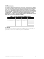
Table 1 provides a list and brief description of the SRMK2 Internet Server’s key features.
Feature
Table 1: Intel® SRMK2S Internet Server key features
Description
1U chassis
1.70” (height) x 16.75” (width behind bezel) x 24” (depth)
Weight
Approximately 30lbs in-box shipping weight
Power supply
Single 200W AC power supply (200W DC supply comes with the SRMK2D)
Cooling
Nine system fans (Eight 40mm and one 17mm)
Rackmounting
Two midmount and Front mounting brackets or sliding rails (optional)
Hard disk capacity
Support for two 1” U160 Hot Swappable SCSI hard drives for internal
configuration along with an external SCSI channel for external drives
Peripheral bays
Single standard slim diskette drive included with system. Optional slim-line
CD-ROM drive available (works in conjunction with the standard diskette).
Peripheral Interfaces
Two Ultra 160 SCSI channels, one internal and one external (The internal
channel has two SCA2 connector ports out the front of the machine)
One IDE interface with UDMA support
One rear serial port
Two 10/100 82559 LAN Connectors
One slim-line diskette interface
LED Panel Interface
Two USB ports
Video Interface
Two PS/2 ports
Microprocessor
Dual Pentium® III processors in PGA370 sockets
Memory capacity
Up to 4 GB of registered PC-100 or PC-133 ECC SDRAM DIMMs
LAN support
Integrated dual Intel® 82559 Pro/100+ Ethernet controllers featuring PXE 2.0 option
ROM for network installation and booting of operating systems
Add-in card support
Passive PCI riser (64-bit/66MHz) supports a low -profile and a full-length (13”) PCI
card
System management
Two Heceta 3 hardware monitoring ASIC’s which work in conjunction with Webbased management software (ASM).
BIOS
Intel/AMI BIOS with extensions to enhance server management capabilities
Intel® SRMK2 Internet Server Technical Product Specification
11
<This page was intentionally left blank>
Intel® SRMK2 Internet Server Technical Product Specification
12
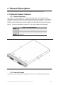
2 Chassis Description
This section describes the features of the Intel® SRMK2 Internet Server chassis.
2.1 External Chassis Features
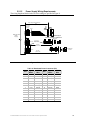
2.1.1 Chassis Dimensions
The chassis is 1.70 inches high by 16.75 inches wide behind the bezel by 24.00 inches deep
(measured from the front of the bezel to the deepest portion of the rear bulkhead). The chassis is
designed to be mounted in a relay-style rack using the two right-angle midmount or front mount
brackets provided with the base system that attach to the chassis and two brackets that attach to
the rack . It can also be installed in a standard 19” rack using a sliding rails kit (Optional).
Table 2: Chassis dimensions
Height
1.70” (1U)
Width
16.75” between the slide mounting surfaces
Depth
24” including bezel, 22.41” from front mounting flange to the rear panel
Shipping
Weight
30lbs. maximum configuration (Fully loaded weight including box and all
accessories)
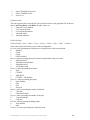
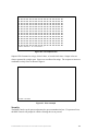
Figure 1: Isometric View of Chassis
2.1.2 Colors of Chassis
The primary exterior of the chassis is unpainted. The bezel is a molded black (GE701) plastic.
Intel® SRMK2 Internet Server Technical Product Specification
13
2.1.3 Front View of Chassis
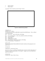
The front bezel is a multiple -part plastic molding that contains the buttons, the LED indicator light
pipes, and a flip-down door that spans half the width of the bezel and folds down (right striated
portion in Figure 2 below). After pulling the flip door down the Power, Sleep, and Reset buttons
as well as the NMI pin hole are revealed. This also reveals the floppy and CD-ROM bays. See
Figure 3 for button placement. See Section 5 Front Panel Board for a complete description of the
buttons and LEDs.
Figure 2: Front view of chassis with bezel on
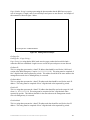
Additionally, the front bezel can be removed to reveal the front of the chassis. To access the hot
swappable SCSI hard disk drives, pivot the front panel out and to the right. Figure 3 shows the
chassis with the front bezel removed and the front panel in the closed position.
Figure 3: Front view of chassis without bezel
Upon pivoting the front panel out and to the right, the SCSI hard disk drive bays are revealed as
shown in Figure 4 below.
Intel® SRMK2 Internet Server Technical Product Specification
14
A
Hot Swappable SCSI Drives
C
Slimline Floppy
B
Slimline CDROM (Optional)
Figure 4 : Front view of chassis without bezel (Does not show Front Panel swung out)
2.1.4 Rear View of Chassis
The input/output connectors are accessible at the back panel of the chassis as shown in Figure 5.
See Section 3.17.1 Back Panel I/O Connectors for detailed descriptions of the rear panel I/O
connectors.
A
B
PS/2 Kbd / Mouse
Video
D
E
USB
Serial Port A
G
H
Low Profile PCI slot
Full Length PCI slot
C
Dual RJ-45
F
U160 SCSI
I
Power Supply *
* The power supply in the SRMK2D has a different connector
Figure 5: Rear view of chassis
2.2 Internal Chassis Features
2.2.1 AC Power Supply
The SRMK2 Internet Server can use two different power supplies, one being an AC 200W
version which ships with the SRMK2S model and a –48V DC 200W version that ships with the
SRMK2D model. For information on the DC model, see the Section 2.2.2 entitled DC Power
Supply. The AC power supply uses a standard IEC 320 power cord and is a single auto-ranging
power factor corrected power supply. The AC power supply rating is described in Table 3.
Intel® SRMK2 Internet Server Technical Product Specification
15
Table 3: 200W power supply output summary
DC Power
+3.3VDC at 13.0A Max.
+5 VDC at 22A Max.
+12 VDC at 3.5A Max.
-12 VDC at 0.25A
5V Standby 1A
Total power from supply
202.9W
AC line voltage
90-135,180-265VAC PFC: auto sense
AC line frequency
47 / 63 Hz
2.2.1.1
Power Supply Mechanical Outline
Both AC and DC power supplies are 3.30”wide by 1.60” high by 9.60”in length. The output cable
bundle is separated into two cables; one cable with two connectors for the serverboard, and the
other with a connector for the backplane which in turn powers the HDD’s. The backplane also
has a CDROM power connector.
2.2.1.2
Power Supply Fan Requirements
The power supply relies on cooling provided by two 40mm fans mounted in the chassis in front of
the power supply. These fans are monitored by hardware on the motherboard and the Advanced
Server Management software that comes on the Resource CD in the accessory kit.
2.2.1.3
AC Power Line
The system is specified to operate over two input voltage ranges that are automatically selected
and rated from 100-120VAC and 200-240VAC, at 50 or 60Hz. The power supply incorporates
Power Factor Correction (PFC) as a standard feature. The system is tested to meet these line
voltages, and has been tested (but not specified) at +10% and -10% of the voltage ranges, and ±
3Hz on the line input frequency. The system is specified to operate without error with line source
interruptions not to exceed 20 milliseconds at nominal line conditions and full power supply output
load. The system is not damaged by AC surge ring wave to 2.5kV/500A. This ring wave is a
100kHz damped oscillatory wave with a specified rise-time for the linear portion of the initial halfcycle of 0.5µsec. Additionally, the system will not be damaged by a unidirectional surge
waveform of 2.0kV /3000A, with a 1.2µsec rise time and 50µsec duration. Further details on
these waveforms can be obtained in ANSI/IEEE STD C62.45-1987.
Intel® SRMK2 Internet Server Technical Product Specification
16
2.2.1.4
DC Connector Requirements
Figure 6 and Figure 7 show the connector pinouts for the serverboard power connectors. These
mate with the power supply connectors at connector J27 and J39.
1 13
Ground
VRM Input Voltage
Ground
VRM Input Voltage
Ground
VRM Input Voltage
Ground
VRM Input Voltage
+3.3V
Ground
+3.3V
Ground
+3.3V
Ground
+3.3V
Ground
Ground
+5V
Ground
+5V
+5VSB
Ground
Ground
+12V
12 24
Figure 6: DC connector pinout (J27)
1
6
HECALERT#
SMB_Data
SMB_CLK
Ground
Ground Sense
+3.3V Sense
PWR_ON#
PWRGOOD
+5V Sense
-12V
5 10
Figure 7: DC connector pinout (J39)
Intel® SRMK2 Internet Server Technical Product Specification
17
2.2.1.5
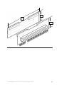
Power Supply Wiring Requirements
The wiring length and the desired wire color-coding are specified in Figure 8.
Edge of supply to center of connector on
PCB.
3.5" (87.5mm)
Only one wire tie
at exit of supply
this bundle.
Wire exit hole in
power
supply.
pin 13
P2
Main
Board
pin 1
Bundle A
Wire lengths should vary to
ensure no loops or slack wire.
0.25"
Max
Main board 2
Conn.
P3
Bundle B
Mini wire ties at
one inch spacing
length of bundle.
3.5" ±0.25"
(87.5mm ±6mm)
P4
Bundle C
SCSI Backplane
Connector
7.75" ±0.25"
(196mm ±6mm)
Figure 8: DC output wire harness
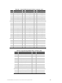
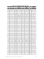
Table 4: Baseboard Power Connector (P2)
Signal 20 AWG
Signal
20 AWG
Pin
Pin
Name
Wire
Name
Wire
1
Ground
Black
13
VRM Input
Red
2
Ground
Black
14
VRM Input
Red
3
Ground
Black
15
VRM Input
Red
4
Ground
Black
16
VRM Input
Red
5
+3.3V
Orange
17
Ground
Black
6
+3.3V
Orange
18
Ground
Black
7
+3.3V
Orange
19
Ground
Black
8
+3.3V
Orange
20
Ground
Black
9
Ground
Black
21
+5V
Red
10
Ground
Black
22
+5V
Red
11
+5VSB
Purple
23
Ground
Black
12
Ground
Black
24
+12V
Yellow
Intel® SRMK2 Internet Server Technical Product Specification
18
Pin
Table 5: Baseboard Power Connector (P3)
Signal Name 20 AWG Wire
Pin
Signal Name
20 AWG Wire
1
HECALERT#*
N/A
6
SMB_Data*
N/A
2
Ground
Black
7
SMB_CLK*
N/A
3
Ground Sense
Black
8
+3.3V Sense
Brown
4
PWR_ON#
Green
9
PWRGOOD
Grey
5
-12V
Blue
10
+5V Sense
Red
* These pins are not stuffed or used on the SRMK2 power supply
Table 6: SCSI Backplane Power Connector (P4)
Pin Signal Name 20 AWG Wire
1
+12V
Yellow
2
+12V
Yellow
3
Ground
Black
4
Ground
Black
5
+3.3V
Orange
6
+5V
Red
2.2.2 DC Power Supply
The SRMK2D model ships with a –48V DC power supply. The output of the DC power supply is
electrically identical to that of the AC power supply (see Table 3 for reference), it shares the
same physical dimensions as the AC power supply, the same mounting, and the same power
cabling to the motherboard. It does vary, however, in it’s electrical specification for line input and
has a different interface on the rear of the chassis than the AC module. The interface on the
back of the DC power supply has four phillips screws that are protected by a cover for shipping.
Removing the cover reveals the four screws. A label should show the screw markings to be: A+
A- B+ B- . The A+ and A- connectors can be attached to a primary power source for the
server, while the B+ and B- leads can be connected to a secondary power source for redundant
power sourcing in case of primary source failure. Table 7 shows the input parameters for the –
48V DC power supply.
Table 7: -48V DC Power Supply Input Parameters
Parameter
Min
Nom
Max
Unit
Vin (-48VDC)
-36.0
-48.0
-72.0
VDC
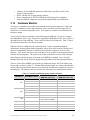
2.2.3 BTU information
BTU’s (British Thermal Units) are a standard for measuring the thermal output of a device. For
reference, one BTU equals the heat that will raise the temperature of one pound of water by one
degree Fahrenheit. In physical terms, 1 BTU = 1054 joules. Listed below is the maximum BTU
output of the SRMK2 system and a loaded system BTU output. System configuration of the
loaded system is described in Table 9.
The BTU maximum rating was derived by taking the maximum wattage output of the power
supply (202.9W), dividing it by the lowest efficiency of the power supply (70% or 0.70) and
multiplying by the BTU conversion number of 3.41. Remember that these numbers are rated at
Intel® SRMK2 Internet Server Technical Product Specification
19
the worst case (lowest efficiency) of the power supply. Under nominal conditions the power
supply should perform above the 70% efficiency level which will lower the BTU rating.
Table 8: Overall BTU Ratings
BTU (Loaded)
BTU (Max)
314 BTU
988 BTU
Table 9: Loaded System Configuration
Manufacturer /
Device
Configuration
Type
CPU #1
733MHz (133 FSB)
Intel Pentium III
CPU #2
733MHz (133 FSB)
Intel Pentium III
Memory
256MB
Micron 133
HDD #1
SCSI 9.1GB
Quantum Atlas V
HDD #2
SCSI 9.1GB
Quantum Atlas V
CD
Slimline CD
Teac CD224EB
Floppy
Slimline Floppy
Sony MPF 720-3
Table 10: Loaded System Power Draw
Current
Voltage Rail
Power (W)
(Measured)
+3.3V
4.1A
13.53 W
+5V
6.7A
33.5 W
-5V
0.1A
0.5 W
+12V
1.3A
15.6 W
-12V
0.1A
1.2 W
+5VSB
0.1A
0.5 W
Total
64.83 W
2.2.4 System Cooling
Nine 40mm fans provide cooling for the system. Two of the nine fans are dedicated to cooling the
power supply. Six of the fans provide cooling for the processor, memory, and serverboard. One
fan cools the full-length PCI slot (this last fan is 40mm x 17mm and is a bit thinner than the other
40mm x 28mm fans). A two-speed control circuit powers the fans and is located on the SCSI
backplane. The control circuit is driven by a sensor that is located on the front panel to monitor
the incoming air temperature. The fans have a tachometer output that can be sampled through the
ServerWorks ® ServerSet™ III LE chipset. The fans can be replaced by removing the top cover,
unplugging the fan connector from the serverboard, lifting the fan out of the fan bracket, and then
inserting the new fan. Additionally, a baffle will be added to help keep the processors and the
memory cool. You should always replace the baffle in the system when you are through working
on the system.
Intel® SRMK2 Internet Server Technical Product Specification
20
2.2.5 System Peripheral Bays
2.2.5.1
CD-ROM and Diskette Drive Bay
The right side of the system (as viewed from the front) contains the CD-ROM and diskette drive
bays. Opening the door in the bezel exposes these peripherals. A slim-line diskette drive is
provided with the system and a slim-line CD-ROM is an optional addition. For information on how
to add/remove the CD-ROM and floppy, please refer to the instruction sheet that comes with the
optional CD-ROM.
2.2.5.2
Internal 3.5” SCSI Hard Drive Bay
Space is provided for two 3.5” long, 1-inch thick hard drives. There are two removable Hudson
drive carriers provided that slide into two front disk drive bays on the front left side of the chassis
(behind the removable front bezel). Each drive can be accessed and replaced by removing the
front bezel, rotating the front panel out of the way (See Figure 3), releasing the handle on the
HDD carrier, and pulling the carrier from the drive bay. A pair of LEDs on the front panel flash
green to indicate drive activity for each drive (LED’s 8 and 9). In addition, the two SCSI HDD
bays are hot swappable.
2.2.6 System Interconnection
2.2.6.1
System Internal Cables
Table 11 lists the internal cables within the system. An italicized item is an optional accessory kit
and is not supplied with the base system.
Cable Purpose
Table 11: System internal cables
Description
Qty
SCSI hard drives
1
Standard 68-pin Wide SCSI cable with a LVD/SE terminator which connects
to the serverboard and the SCSI backplane
Front panel
1
50-pin flex cable; connects from front panel connector on the serverboard
to the front panel board.
Fan backplane
1
High density cable connects from the serverboard to the backplane to
provide system management monitoring of the system fans.
Slim-line diskette drive
1
26-pin flex cable; connects from high-density diskette drive connector on
the serverboard to one slim-line diskette drive
Slim-line CD-ROM
drive*
1
Standard 40-pin IDE cable with 2 connectors; connects from secondary IDE
connector on the serverboard to one slim-line CD-ROM drive
* Optional Accessory
Intel® SRMK2 Internet Server Technical Product Specification
21
2.2.6.2
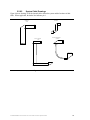
System Cable Drawings
Figure 9 shows drawings of all the internal cables within the system and the locations of their
folds. Where applicable, the darker line indicates pin 1.
Front panel
SCSI hard
drives
Slim-line diskette
drive
Slim-line CD-ROM drive
(optional)
Figure 9: Internal cables
Intel® SRMK2 Internet Server Technical Product Specification
22
2.3 System Configuration
Table 12 lists the base configuration of the SRMK2S Internet Server.
Table 12: Standard configuration
Description
Qty
SRMK2 serverboard
1
Dual-slot 66/64 PCI riser
1
Front panel board
1
200W power supply
1
System fans
9
SCSI Hard drive carriers
2
3.5” slime-line diskette drive with bracket
1
SCSI Hot swap backplane
1
SCSI backplane cable
1
Slimline floppy diskette drive cable
1
Front panel cable
1
Fan backplane cable
1
Front and Midmount brackets *
2
Heatsinks *
2
* Items that come in the Accessory Kit
Table 13 lists optional accessories. These accessories can be ordered:
Table 13: Optional accessories
Description
Product Code
Qty
Slim-line CD-ROM comes with one IDE
cable, installation instructions, and
backplane for slim-line CD-ROM drive
ACCCDROM001
1
Jonathan Manufacturing sliding rail kit
ACCRAILKIT001
1
Intel® SRMK2 Internet Server Technical Product Specification
23
3 SRMK2 Serverboard Description
3.1 Overview
The SRMK2 serverboard features are summarized in Table 14.
Table 14: SRMK2 feature summary
Form Factor
Serverboard dimension: 10.4” x 11.3”
Processor
Supports Dual Pentium® III processors using PGA370 sockets
Memory
•
Four 168-pin dual inline memory module (DIMM) sockets
•
Supports only registered SDRAM DIMMs
•
Supports up to 4 GB of ECC, SPD Registered SDRAM DIMMs
Chipset
ServerWorks® ServerSet™III LE Chipset, consists of:
•
ServerWorks CNB30LE North Bridge Front Side Bus Interface chip
•
ServerWorks OSB4 South Bridge chip
I/O Control
SMSC FDC37B782 I/O controller
Peripheral
Interfaces
•
Two integrated Intel® 82559 10/100BASE-T Ethernet controllers
•
One high-density diskette drive interface for slimline diskette drive
•
Two U160 SCSI channels (one internal and one external wide interface connector)
•
One IDE interface with low profile CD support
•
One serial port
•
Two USB ports
•
Two PS/2 interfaces for keyboard and mouse
•
LED panel interface
•
One rear panel video interface
Expansion
Capabilities
One 64/66 plug-in riser card expansion PCI bus slot which can fit a 2x11 riser sideband
connector supporting two PCI slots – One full length card and the other low profile.
BIOS
•
Intel/AMI BIOS
•
Intel® 8-Mbit boot block flash memory
•
Supports SMBIOS, Advanced Configuration and Power Interface (ACPI), and Plug and Play
(see section 14.2 Specifications for specification compliance levels)
•
Speaker
•
(2) Hardware monitor chips
•
Wake on Ring
•
Wake on LAN
•
SCSI LED connector
Other Features
Intel® SRMK2 Internet Server Technical Product Specification
24
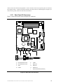
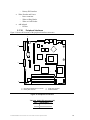
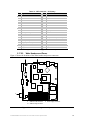
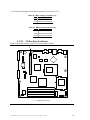
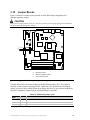
3.2 Serverboard Layout
Figure 10 shows the location of the major components on the serverboard.
I
A B C D E F GH
J
K
BB
L
M
AA
N
Z
Y
X
W
O
V
P
U T S
A
B
C
D
E
F
G
H
I
J
K
L
M
Battery
Slimline Floppy Connector
Wake on LAN Header
Speaker
Clear Password Jumper
64/66 PCI Bridge Connector
ServerWorks ® ServerSet™ South Bridge
BIOS Flash memory
Back panel I/O connectors
SMSC I/O controller
Wake on Ring Header
ATI Rage XL Video
Intel® 82559 10/100 Ethernet controllers
Q
R
N
O
P
Q
R
S
T
U
V
W
X
Y
Z
AA
BB
PGA370 processor sockets
Heceta 3 hardware monitor controllers
Fan backplane connector
Front panel connector
DIMM sockets
SCSI LED Header
Gluechip
Power supply connector
ServerWorks® ServerSet™ North Bridge
Adaptec® 7899 SCSI controller
Password override jumper
Clock generator
Whitebox / Appliance Jumper
Internal SCSI connector
Primary IDE connector
Figure 10: Serverboard components
Intel® SRMK2 Internet Server Technical Product Specification
25
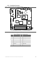
Figure 11 is a block diagram of the SRMK2 serverboard.
Processor
Processor
CNB30LE
SDRAM
DIMMs
Dual-Slot
64/66 PCI
Riser
Clock
Generator
Hardware
Monitor
Hardware
Monitor
SM
Bus
32/33 PCI Bus
Pri IDE
ATI Rage XL
Video
Controller
Back Panel
Adaptec 7899
Dual Channel
SCSI
Dual 82559
Ethernet
Controllers
Back Panel
Back Panel
64/66 PCI Bus
USB Port 0
OSB4
Front Drive
Bay
USB Port 1
Back Panel
ISA Bus
Boot Block
Flash Memory
Serial Port A
FDC37B782
I/O Controller
Front Panel
Controller
Mouse
Keyboard
Front Panel
Back Panel
Diskette
Back Panel
Figure 11: Serverboard block diagram
Intel® SRMK2 Internet Server Technical Product Specification
26
3.3 Processors
The SRMK2 serverboard supports dual Pentium® III processors. The host bus speed (100 MHz
or 133 MHz) is automatically selected based on the speed of the processors placed in the PGA370
sockets. The processors must be secured by pushing the Zero-Insertion-Force (ZIF) socket’s
lever down. The Intel SRMK2 serverboard can run in either a Uniprocessor (UP) mode or Dual
Processor (DP) mode. A terminator must be placed in the second processor PGA370 socket for
UP mode operation. A terminator card is shipped with the unit and is installed in the second
processor socket in the factory. Remove the terminator card if you wish to run in dual processor
mode. Table 15 lists processors supported by the SRMK2.
Table 15: Processors supported by the SRMK2S serverboard
Processor Type
L2 Cache Size
FSB Speed
Speed
Pentium® III
256 KB
100 MHz
Pentium® III
256 KB
133 MHz
800 MHz
1.0 GHz
933 MHz
866 MHz
800 MHz
733 MHz
!
NOTE
The serverboard supports Pentium® III processors with a 133 MHz host bus. The serverboard may not
operate reliably if a processor with a 133 MHz host is paired with 100 MHz SDRAM.
Intel® SRMK2 Internet Server Technical Product Specification
27
3.4 Chipset
The ServerWorks ® ServerSet™ III LE chipset consists of the ServerWorks CNB30LE North
Bridge chip and the ServerWorks OSB4 South Bridge chip. The CNB30LE provides an optimized
DRAM controller. The I/O subsystem of the ServerWorks chipset is based on the OSB4 South
Bridge, which is a highly integrated PCI ISA IDE Xcelerator Bridge.
3.4.1 ServerWorks CNB30LE North Bridge Chip
The ServerWorks CNB30LE North Bridge chip provides bus-control signals, address paths, and
data paths for transfers between the processor’s host bus, the PCI bus, and main memory.
The North Bridge features:
Processor Interface Control
•
Support for processor host bus frequency of 100MHz and 133MHz
•
32-bit addressing
•
Desktop-optimized GTL+ compliant host bus interface
Integrated DRAM Controller
•
+3.3V only DIMM DRAM configurations
•
Up to four double -sided DIMMs
•
100MHz or 133MHz SDRAM
•
Support for up to 4GB of registered SDRAM
•
DIMM serial presence detect via SMBus interface
•
16-, 64- and 128-Mbit devices with 2 KB, 4 KB, and 8 KB page sizes
•
x 4, x 8, and x 16 DRAM widths
•
Single error correction, multiple error detection
•
Symmetrical and asymmetrical DRAM addressing
•
ECC SEC/DED
PCI Bus Interface
•
Complies with the PCI specification Rev. 2.1
•
64 bit, 33/66 MHz Secondary PCI bus interface with integrated PCI arbiter
•
Asynchronous coupling to the host-bus frequency
•
PCI parity generation support
•
Data streaming support from PCI-to-DRAM
•
Support for four PCI bus masters in addition to the host and PCI-to-ISA I/O bridge
•
Support for concurrent host and PCI transactions to main memory
Data Buffering
•
DRAM write buffer with read-around-write capability
•
Dedicated host-to-DRAM, PCI0-to-DRAM, and PCI1-to-DRAM read buffers
Power Management
•
Support for system suspend/resume
•
Compliant with ACPI power management
SMBus Support for desktop management functions
Support for System Management Mode (SMM)
Glueless Serial interface with OSB4 South Bridge chip
Intel® SRMK2 Internet Server Technical Product Specification
28
3.4.2 ServerWorks OSB4 South Bridge Chip
The OSB4 South Bridge chip is a multifunctional PCI device implementing the PCI-to-ISA bridge,
PCI IDE functionality, USB host/hub functionality, and enhanced power management. The OSB4
South Bridge features:
•
•
•
•
•
•
•
•
•
•
•
•
•
•
•
•
•
•
•
•
Multifunctional PCI-to-ISA Address / Data bridge
PCI Slave
PCI Arbiter
PCI Master
Full ISA bus support
ISA Arbiter
One 8253 Counter/Timer
Client Management
– Temperature Sensing Inputs
– Two I2C Bit Bang Interfaces for (GPOC)
– Four general purpose I/O (GPMs)
Support for the PCI bus at 33 MHz
Support for PCI Rev 2.1 Specification
Integrated dual-channel enhanced IDE interface
– Support for up to four IDE devices
– PIO Mode 4 transfers at up to 16 MB/sec
– Support for Ultra DMA/33 synchronous DMA mode transfers at up to 33 MB/sec
– Bus master mode with an 8 x 32-bit buffer for bus master PCI IDE burst transfers
Enhanced DMA controller
– Two 8237-based DMA controllers
– Support for PCI DMA with three PC/PCI channels and distributed DMA protocols
– Fast type-F DMA for reduced PCI bus usage
Interrupt controller based on 82C59
– Support for 15 interrupts
– Programmable for edge/level sensitivity
Power management logic
– Sleep/resume logic
– Support for Wake on Ring and Wake on LAN† technology
– Support for APM and ACPI Revision 1.0
Internal APIC Controller
USB Interface
SMB bus interface
Glueless Serial interface with CNB30LE North Bridge chip
Black Box Security Functions
– 2X Passwords
– CMOS Protection
– Super I/O Security
Real-Time Clock
– 256-byte battery-backed CMOS SRAM
– Date alarm
– 16-bit counters/timers based on 82C54
Intel® SRMK2 Internet Server Technical Product Specification
29
3.5 Memory
The serverboard has four DIMM sockets. The serial presence detect (SPD) data structure which
is programmed into an E2PROM on the DIMM instructs the BIOS on the SDRAM’s size and
speed. The minimum memory size is 64MB; the maximum memory size is 4GB. DIMMs can be
populated in any order, but due to the 25 degree angle of the DIMM socket mountings it is
physically easier to populate DIMMs starting with DIMM0 and moving towards DIMM3.
Memory size can vary between sockets and slot vacancy between DIMMs is permitted. Mixing
of DIMM size is allowed as long as they are all registered DIMMs. For a list of compatible tested
memory please visit the support site at support.intel.com.
The serverboard supports the following memory features:
•
•
•
•
DIMM
Size
168-pin SPD DIMMs with gold-plated contacts.
133 MHz and 100 MHz registered SDRAM DIMMs, 72-bit ECC, 3.3V memory.
Single- or double-sided DIMMs in the sizes listed in Table 16.
Registered DIMMs of the following sizes: 64M, 128M, 256M, 512M and 1G for a
maximum memory size of 4 GB. Double stacked DIMMs may only be used if they
are within the 4.33 mm maximum thickness imposed by the 25 degree DIMM socket
spacing on the baseboard.
Table 16: Supported memory sizes and configurations
Configuration
DRAM
DRAM DRAM
Single-sided
Technology Depth
Width
DIMM Size x 64
bit
64 MB
8 Mbit x 72
64Mb
4Mb
16 bit
X
Double-sided
DIMM Size x 64
bit
8MB X 8B = 64MB
64 MB
8 Mbit x 72
64Mb
8Mb
8 bit
8MB X 8B = 64MB
X
128 MB
16 Mbit x 72
64Mb
8Mb
8 bit
X
16MB X 8B = 128MB
128 MB
16 Mbit x 72
64Mb
16Mb
4 bit
16MB X 8B = 128MB
X
64 MB
8 Mbit x 72
128Mb
8Mb
16 bit
8MB X 8B = 64MB
X
128 MB
16 Mbit x 72
128Mb
8Mb
16 bit
X
16MB X 8B = 128MB
128 MB
16 Mbit x 72
128Mb
16Mb
8 bit
16MB X 8B = 128MB
X
256 MB
32 Mbit x 72
128Mb
16Mb
8 bit
X
32MB X 8B = 256MB
256 MB
32 Mbit x 72
128Mb
32Mb
4 bit
32MB X 8B = 256MB
X
64 MB
8 Mbit x 72
256Mb
8Mb
32 bit
8MB X 8B = 64MB
X
128MB
16 Mbit x 72
256Mb
8Mb
32 bit
X
16MB X 8B = 128MB
128 MB
16 Mbit x 72
256Mb
16Mb
16 bit
16MB X 8B = 128MB
X
256MB
32 Mbit x 72
256Mb
16Mb
16 bit
X
32MB X 8B = 256MB
256 MB
32 Mbit x 72
256Mb
32Mb
8 bit
32MB X 8B = 256MB
X
512 MB
64 Mbit x 72
256Mb
32Mb
8 bit
X
64MB X 8B = 512MB
512 MB
64 Mbit x 72
256Mb
64Mb
4 bit
64MB X 8B = 512MB
X
1GB
128 Mbit x 72
256Mb
64Mb
4 bit
X
!
128MB X 8B = 1GB
NOTE
All memory components and DIMMs used with this motherboard must comply with the following
PC SDRAM specifications:
• PC SDRAM Specification (memory component specific)
• PC SDRAM Registered DIMM Specification
Intel® SRMK2 Internet Server Technical Product Specification
30
3.6 SCSI Host bus Interface
The SRMK2 motherboard uses an Adaptec® AIC-7899 Ultra 160 SCSI controller for the SCSI
Host bus interface. The AIC provides two independent Ultra 160/m SCSI channels combined with
a full-featured PCI 2.1/2.2-compliant bus master. The AIC-7899 operates at up to 66MHz and
functions as a 64-bit bus master capable of supporting zero wait state 64-bit memory transfers at a
maximum data burst rate of 533 Mbytes/sec. The AIC-7899 SCSI controller complies with the
SCSI-3 standard providing multimode SCSI support for both single -ended (SE) and Low Voltage
Differential (LVD) SCSI peripherals. The SRMK2 motherboard has two SCSI Ultra 160, 68-pin
D-shell connectors, one internal and one external on the rear panel. Both SCSI connectors are
protected from over-current conditions via a separate polyfuse.
3.6.1 SCSI Hard Drive LED Connector (Optional)
The optional SCSI hard drive LED connector is a 1 x 2-pin connector that allows add-in
SCSI controller applications to use the same LED as the IDE controller. This connector
can be connected to the LED output of the add-in controller card (J35 is the designator
number on the motherboard)
3.7 IDE Interface
Through the ServerWorks ® ServerSet™ OSB4 South bridge, the serverboard has one independent
bus-mastering IDE interface. This interface supports:
•
•
ATAPI devices (such as CD-ROM drives)
ATA devices
One 40-pin connector is populated on board. The connector at J9 provides the primary IDE
interface (only this one is populated). The BIOS supports logical block addressing (LBA) and
extended cylinder head sector (ECHS) translation modes. The drive reports the transfer rate and
translation mode to the BIOS.
3.8 USB
The serverboard has two USB ports; one USB peripheral can be connected to each port. For
more than two USB devices, an external hub can be connected to either port. The two USB ports
are implemented with stacked back panel I/O connectors. The serverboard fully supports UHCI
and uses UHCI-compatible software drivers. See section 14.2 for information about the USB and
UHCI specifications. (Note that NT 4.0 does not have USB support). Additionally, Legacy
USB devices are not supported by the system BIOS. This means that a Legacy USB keyboard
will not be operable during the system POST and you will not be able to enter the system BIOS
with a Legacy USB keyboard because of this restriction. To work around this problem, use a
PS/2 keyboard for changing BIOS settings. This restriction does not affect the use of Legacy
USB keyboards under operating systems that support USB devices.
The SRMK2 USB ports feature:
•
•
Self-identifying peripherals that can be plugged in while the computer is running
Automatic mapping of function to driver and configuration
Intel® SRMK2 Internet Server Technical Product Specification
31
•
•
•
!
Support for isochronous and asynchronous transfer types over the same set of wires
Guaranteed bandwidth and low latencies appropriate for telephony, audio, and other
applications
Error-handling and fault-recovery mechanisms built into the protocol
NOTE
Computer systems that have an unshielded cable attached to a USB port may not meet FCC Class B
requirements, even if no device or a low-speed USB device is attached to the cable. Use shielded cable that
meets the requirements for full-speed devices.
3.9 I/O Controller
The FDC37B782 I/O controller from SMSC is an ISA Plug and Play-compatible, multifunctional
I/O device that provides the following features:
•
•
•
•
•
One serial port
FIFO support on both serial and diskette drive interfaces
PS/2-style mouse and keyboard interfaces
Support for serial IRQ packet protocol
Intelligent power management, including:
−
Shadowed write-only registers for ACPI compliance
−
Programmable wake up event interface
3.9.1 Serial Port
The motherboard supports one serial port via 9-pin D-Sub connector. The populated serial port is
located on the back panel. The serial port is NS16C550-compatible UARTs and support data
transfers at speeds up to 460 Kbits/sec with BIOS support. Additionally, this port supports the
Wake On Ring functionality.
3.9.2 Diskette Drive Controller
The I/O controller supports a single diskette drive that is compatible with the 82077 diskette drive
controller and support both PC-AT† and PS/2 modes. The baseboard supports only a slimline
floppy drive interface connector.
3.9.3 Keyboard and Mouse Interface
The PS/2 keyboard and mouse connectors are located on the back panel. The +5V lines to these
connectors are protected with a PolySwitch† circuit that, like a self-healing fuse, reestablishes the
connection after an overcurrent condition is removed.
!
NOTE
The mouse and keyboard can be plugged into either of the PS/2 connectors. Turn off power to
the computer before connecting or disconnecting a keyboard or mouse.
3.9.4 Real-Time Clock, CMOS SRAM, and Battery
The real-time clock is provided by the SMC FDC37B782 Super I/O chip and is compatible with
DS1287 and MC146818 components. The clock provides a time-of-day clock and a multicentury
Intel® SRMK2 Internet Server Technical Product Specification
32
calendar with alarm features and century rollover. The real-time clock supports 256 bytes of
battery-backed CMOS SRAM in two banks that are reserved for BIOS use.
A coin-cell battery powers the real-time clock and CMOS memory. When the computer is not
plugged into a wall socket, the battery has an estimated life of three years. When the computer is
plugged in, the 3.3V standby current from the power supply extends the life of the battery. The
clock is accurate to ± 13 minutes/year at 25ºC with 3.3VSB applied. The time, date, and CMOS
values can be specified in the BIOS Setup program.
!
NOTE
The recommended method of accessing the date in systems with Intel® serverboards is indirectly from the
Real Time Clock (RTC) via the BIOS. The BIOS on Intel® serverboards contains a century checking and
maintenance feature. This feature checks the two least significant digits of the year stored in the RTC
during each BIOS request (INT 1Ah) to read the date and, if less than 80 (i.e., 1980 is the first year supported
by the PC), updates the century byte to 20. This feature enables operating systems and applications using
the BIOS date/time services to reliably manipulate the year as a four-digit value.
For more information on a proper date access in systems with Intel serverboards, please visit:
http://support.intel.com/support/year2000/
3.10
Intel® 82559 10/100 Ethernet Controllers
Two Intel 82559 LAN controllers provide two 10/100 Base-T RJ-45 interfaces. The two LAN
ports are brought out through a double stacked RJ45 connector on the rear of the chassis.
The LAN circuitry supports Wake on LAN technology on both LAN ports. Wake on LAN
technology enables remote wakeup of the computer through a network. If a PCI add-in network
interface card (NIC) with remote wakeup capabilities is desired, the remote wakeup connector on
the NIC must be connected to the onboard Wake on LAN header at J8. The on-board LAN
controllers or an add-in NIC will monitor network traffic at the MII interface; upon detecting a
Magic Packet† the LAN controllers or NIC will assert a wakeup signal that will power up the
computer. Alert and wake on LAN features are supported by the SRMK2 and the SMBus
interface of the Intel 82559s.
CAUTION
For Wake on LAN, the +5V standby line for the power supply must be capable of delivering +5V ± 5% at
720mA. Failure to provide adequate standby current when implementing Wake on LAN can damage the
power supply.
3.11
Video Interface
The on-board video interface is implemented using the ATI RAGE XL video controller. The
video controller is accessed over the 32-bit PCI bus interface on the ServerWorks ® North Bridge.
Some of the key features of the video interface are listed below:
•
•
•
•
•
•
Comprehensive AGP support, including 2X mode, Sideband addressing.
Fully PC 98 compliant.
32-bit wide memory-mapped registers.
Programmable flat or paged memory model with linear frame buffer access.
Triple 8-bit palette DAC with gamma correction for true WYSIWYG color.
Pixel rates up to 230 MHz.
Intel® SRMK2 Internet Server Technical Product Specification
33
•
•
•
•
3.12
4M bytes of video SDRAM organized as 2Mx32-bits, accessible over the 64-bit
interface of the controller.
DDC1 and DDC2B+ for plug and play monitors.
Power management for full VESA DPMS and EPA Energy Star compliance.
Integrated hardware diagnostic tests performed automatically upon initialization.
Hardware Monitor
Two Heceta 3 controllers are provided on the motherboard to monitor temperature, voltage, and
fan speed. In addition to the on chip temperature sensor, each Heceta provides input pins for
connection to an external temperature sensor. These inputs are connected to the Pentium® III
thermistor outputs.
Access to the two Heceta controllers is provided through the SMB bus. Heceta #1 is mapped
onto SMB address [0101 101x]. Heceta #2 is mapped onto SMB address [0101 110x], where x is
the Read/Write bit of the SMB bus. These can also be listed as 0x2d and 0x2e. Table 17 shows
the functions monitored by each Heceta controller.
When the Heceta is configured in the monitoring mode, it cycles sequentially through the
measurement of analog inputs and the temperature sensor, while at the same time the fan speed
inputs are independently monitored. Measured values from these inputs are stored in Value
Registers. These can be read out over the serial bus or can be compared with programmed limits
stored in the Limit Registers. The results of out of limit comparisons are stored in the Interrupt
Status Registers and will generate an interrupt on the INT line, if enabled. Any or all of the
Interrupt Status Bits can be masked by appropriate programming of the Interrupt Mask Register.
There are 9 Fans in the SRMK2 System which are multiplexed into the Fan1/Fan2 inputs of the
Heceta chips, as shown in Table 17. The Mux1/Mux0 control signals are software controlled bits
located in the front panel EPLD and are used to control the fan tachometer multiplexer located on
the Backplane. The software control is located in the Advanced Server Management software.
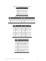
Table 17: Functions monitored by the Heceta controllers
Heceta #1 Function
Heceta #2 Function
Heceta Pin Mux1/Mux0 Control
SMB addr 0101 101x
SMB addr 0101 110x
Fan 1
Fan 2
CHS
+VCCP1
00
Fan Tach 1
Fan Tach 3
01
Fan Tach 5
Fan Tach 7
10
Fan Tach 9
N/A
11
N/A
N/A
00
Fan Tach 2
Fan Tach 4
01
Fan Tach 6
Fan Tach 8
10
N/A
N/A
11
N/A
N/A
Chassis Intrusion
N/A
(Not functional on SRMK2)
VCORE
N/A
+2.5V
VTT
+2.5V
+3.3V
+3.3V
+3.3V STBY
+5V
+5V STBY
+5V
Intel® SRMK2 Internet Server Technical Product Specification
34
+12V
D1+/D1-
+12V
N/A
CPU 0 Thermistor
CPU 1 Thermistor
For more details on accessing the Heceta registers please refer to the ADM1024 data sheet from
Analog Devices.
3.13
Wake on Ring and Resume on Ring
The SRMK2 baseboard provides three methods for implementing Wake on Ring (WOR). An
external modem connected to the serial port can toggle the super I/O controller’s Ring Indicator
pin which should be enabled to cause a wakeup event. The WOR output of an internal modem
card may be connected to an internal 2-pin WOR header (J11) to cause a wakeup event. Finally,
a PCI modem may implement a WOR circuit that uses PCI PME# to cause a wakeup event.
This section describes two technologies that enable telephony devices to access the computer
when it is in a power-managed state. The method used depends on the type of telephony device
(external or internal) and the power management mode being used (APM or ACPI).
/
NOTE
Wake on Ring and Resume on Ring technologies require the support of an operating system that
provides full ACPI functionality.
3.13.1
Wake on Ring
The operation of Wake on Ring can be summarized as follows:
•
•
Powers up the computer from either the APM soft-off mode or the ACPI S5 state
Detects incoming calls differently for external and internal modems:
− For external modems, the serverboard hardware monitors the Ring Indicator (RI)
input of the serial port.
− For internal modems, a cable must be routed from the modem to the Wake on Ring
connector
3.13.2
Resume on Ring
The operation of Resume on Ring can be summarized as follows:
•
•
•
3.14
Resumes operation from either the APM sleep mode or the ACPI S1 to S4 state
Detects incoming calls similarly for external and internal modems; does not use the
Wake on Ring connector.
Requires that modem interrupt be unmasked for correct operation.
Speaker
A 47 Ω inductive speaker is mounted on the motherboard. The speaker provides audible error
code (beep code) information during the power-on self test (POST).
Intel® SRMK2 Internet Server Technical Product Specification
35
3.15
Fan Support
The backplane powers nine 40mm system fans. Additionally, it incorporates logic to control and
monitor the tachometer speed of fans. Eight of those fans are 40mm x 28mm. The ninth fan is
40mm x 17mm and provides cooling to the PCI add-in card area.
3.16
Baseboard Programming
3.16.1
PCI Configuration Space Map
Table 18: PCI Configuration Space Map
Bus
Number
(hex)
Device
Number
(hex)
Function
Number
(hex)
00
00
00
CNB30LE Host Bridge Function 32 bit PCI (P1_AD[16])
00
00
01
CNB30LE 2nd Host Bridge Function 64 Bit PCI (P1_AD[16])
00
01
NA
PCI32 VIDEO (P1_AD[17])
00
02
NA
PCI32 SLOT1 (P1_AD[18])
00
03
NA
PCI32 SLOT2 (P1_AD[19])
00
05
NA
PCI32 LAN1
(P1_AD[23])
00
06
NA
PCI32 LAN2
(P1_AD[24])
00
0F
00
OSB4 SMB Bus, PCI Configuration Registers (P1_AD[31])
00
0F
01
OSB4 Ultra DMA IDE bus master (P1_AD[31])
01
02
NA
PCI64 SLOT1 (P2_AD[18])
01
03
NA
PCI 64 SLOT2 (P2_AD[19])
01
04
NA
PCI 64 SCSI
3.16.2
Description
(P2_AD[20])
Interrupts
Table 19 lists the system interrupts for the SRMK2.
Table 19: PCI Interrupt to OSB4 IRQ Input Mapping
OSB4 Input
PCI Interrupt
PCIIRQ0
LAN1 IRQ#
PCIIRQ1
LAN2 IRQ#
PCIIRQ2
P1S1_INTAC# (PCI32 Slot1 Interrupts A & C)
PCIIRQ3
P1S1_INTBD# (PCI32 Slot1 Interrupts B & D)
PCIIRQ4
P1S2_INTAC# (PCI32 Slot2 Interrupts A & C)
PCIIRQ5
P1S2_INTBD# (PCI32 Slot2 Interrupts B & D)
PCIIRQ6
FP_IRQ# (Front Panel IRQ#)
PCIIRQ7
VID_IRQ# (Video IRQ#)
PCIIRQ8
SCSI_IRQA#
PCIIRQ9
SCSI_IRQB#
PCIIRQ10
P2S1_INTAC# (PCI64 Slot1 Interrupts A & C)
PCIIRQ11
P2S1_INTBD# (PCI64 Slot1 Interrupts B & D)
Intel® SRMK2 Internet Server Technical Product Specification
36
3.16.3
PCIIRQ12
P2S2_INTAC# (PCI64 Slot2 Interrupts A & C)
PCIIRQ13
P2S2_INTBD# (PCI64 Slot2 Interrupts B & D)
PCIIRQ14
Not Used
PCIIRQ15
Not Used
SMI and NMI Routing
There are numerous SMI/NMI sources. SMI/NMI sources are routed either to OSB4 or SIO
GPI input pins. Software must configure the OSB4 and SIO GPI input pins to control whether the
corresponding events will generate SMI, NMI or wake up events to the processors. The
SMI/NMI sources on the SRMK2 are shown in Table 20. Note that some inputs are the wired
OR of several sources. Signal names are in parenthesis.
Table 20: SRMK2 SMI and NMI sources
SMI Source
OSB4 Input Pin
Processor #0 IERR (IERR#0)
GEVENT_0
Processor #1 IERR (IERR#1)
GEVENT_1
Processor #0 Thermal Trip (THERMTRIP#0)
GEVENT_2
Processor #1 Thermal Trip (THERMTRIP#0)
GEVENT_3
CNB30LE Chipset PCI SERR# - used for ECC Errors (SALERT#)
GEVENT_4
Wired OR of HECETA #1 & #2 INT output and LAN 1 & 2 SMBALERT
output (SMBALERT#)
GEVENT_5
Gluechip’s EXTSMI# output – used for +5VSB errors (EXTSMI#)
GEVENT_6
Debug NMI from Front Panel or NMI jumper (DBG_NMI#)
GEVENT_7
SIO SMI (SIO_SMI#)
GEVENT_19
SIO WAKE UP (SIO_WAKEUP#)
SIO_WAKEUP
32-bit PCI SERR (P1_SERR#)
SERR#
64-bit PCI SERR (P2_SERR#)
FRWP#
GEVNT_21
SIO Input Pin
Wired OR of 32-bit PCI PME, External WOL, LAN1 PME, and LAN2 PME
(P1_PME#)
GP17
64-bit PCI PME (P2_PME#)
GP16
Wake on Ring (WOR#)
GP11
3.16.4
System Management Bus (SMB)
The SRMK2 baseboard supports a simple I2C compatible Bus to provide a method to manage
system resources. To implement this feature, the ServerWorks South Bridge device becomes the
master controller and communicates with several other devices in the system. Some of the
functions the processor can monitor though the SMB bus are the following: Fan Speed
(Tachometer), temperatures, voltage rails, LAN controllers, DIMM presence and size. Table 21
shows the address map of the various devices on the SM Bus.
Device
Table 21: SMB Bus Address Map
Master/Slave
I2C Address
OSB4
Master Controller
N/A
LAN Controller 1
Slave
:84
Intel® SRMK2 Internet Server Technical Product Specification
37
LAN Controller 2
Slave
:85
32 PCI Riser expansion Connector
Slave
Undefined **
64 PCI Riser expansion Connector
Slave
Undefined **
Memory DIMM 0
Slave
:50
Memory DIMM 1
Slave
:51
Memory DIMM 2
Slave
:52
Memory DIMM 3
Slave
:53
st
Slave
:2D
nd
2 Heceta System Management chip
Slave
:2E
CNB30LE North Bridge chip
Slave
:C0
1 Heceta Management chip
** Note: At the writing of this document, the PCI riser expansion boards did not have an I 2C bus ID assigned.
3.17
Baseboard Connectors and Jumpers
This section describes the serverboard connectors. The connectors can be divided into three
groups, as shown in Figure 12.
A
B
A
Back panel I/O connectors
B
Midboard connectors
C
Front panel connector
C
Figure 12: Connector groups
CAUTION
Only the back panel connectors of this serverboard have overcurrent protection. The internal serverboard
connectors are not overcurrent protected, and should be connected only to devices inside the computer
Intel® SRMK2 Internet Server Technical Product Specification
38
chassis such as fans and internal peripherals. Do not use these connectors for powering devices external to
the computer chassis. A fault in the load presented by the external devices could damage the computer, the
interconnecting cable, and the external devices themselves.
3.17.1
Back Panel I/O Connectors
Figure 13 shows the location of the back panel I/O connectors.
A
D
F
C
B
E
H
I
G
A
PS/2 keyboard or mouse
E
LAN #1
B
C
PS/2 keyboard or mouse
F
USB port 0
Video
G
USB port 1
D
LAN #2
H
Serial Port A
I
68-pin External SCSI (Channel A)
Figure 13: Back panel I/O connectors
Intel® SRMK2 Internet Server Technical Product Specification
39
Table 22: PS/2 keyboard/mouse connectors (J7)
Pin Signal Name
Pin
1
Keyboard or Mouse Data
2
Not connected
3
Ground
4
Fused +5 V
5
Keyboard or Mouse Clock
6
Not connected
Table 23: USB stacked connector (J2)
Signal Name
Pin Signal Name
1
Fused +5 V
5
Fused +5 V
2
3.3 V differential USB signal USB_D-
6
3.3 V differential USB signal USB_D-
3
3.3 V differential USB signal USB_D+
7
3.3 V differential USB signal USB_D+
4
Ground
8
Ground
Note: J2 (top) is port #0 and J2 (bottom) is port #1.
Pin
Table 24: LAN RJ45 connectors (J5)
Signal Name
Pin
Signal Name
1
TX+
1
TX+
2
TX-
2
TX-
3
RX+
3
RX+
4
Return
4
Return
5
Return
5
Return
6
RX-
6
RX-
7
Return
7
Return
Return
8
Return
8
Note: J5-A (bottom) is LAN #1 and J5-B (top) is LAN #2.
Table 25: Serial port A connector (J3)
Pin
Signal Name
1
DCD (Data Carrier Detect)
2
SIN # (Serial Data In)
3
SOUT # (Serial Data Out)
4
DTR (Data Terminal Ready)
5
Ground
6
DSR (Data Set Ready)
7
RTS (Request to Send)
8
CTS (Clear to Send)
9
RI (Ring Indicator)
Intel® SRMK2 Internet Server Technical Product Specification
40
Pin
Pin
Table 26: Video connector (J4)
Signal Name
Pin
Signal Name
1
V_RED_FB
2
V_GREEN_FB
3
V_BLUE_FB
4
TP_VIO4
5
GRD
6
GRD
7
GRD
8
GRD
9
TP_VIO9
10
GRD
11
(Not Connected)
12
DDC2_SDA
13
V_HSYNC_R#
14
V_VSYNC_R#
15
DDC2_SCL
Table 27: External SCSI (Channel A) connector (J1)
Signal Name
Pin Signal Name
Pin Signal Name
1
SDA[12]+
2
SDA[13]+
3
SDA[14]+
4
SDA[15]+
5
SDA[P1]+
6
SDA[0]+
7
SDA[1]+
8
SDA[2]+
9
SDA[3]+
10
SDA[4]+
11
SDA[5]+
12
SDA[6]+
13
SDA[7]+
14
SDA[P0]+
15
GRD
16
DIFFSA
17
SCSIA_5V
18
SCSIA_5V
19
EXT_SCSI_P19_NC
20
GRD
21
ATNA+
22
GRD
23
BSYA+
24
ACKA+
25
RSTA+
26
MSGA+
27
SELA+
28
CDA+
29
REQA+
30
IOA+
31
SDA[8]+
32
SDA[9]+
33
SDA[10]+
34
SDA[11]+
35
SDA[12]-
36
SDA[13]-
37
SDA[14]-
38
SDA[15]-
39
SDA[P1]-
40
SDA[0]-
41
SDA[1]-
42
SDA[2]-
43
SDA[3]-
44
SDA[4]-
45
SDA[5]-
46
SDA[6]-
47
SDA[7]-
48
SDA[P0]-
49
GRD
50
GRD
51
SCSIA_5V
52
SCSIA_5V
53
EXT_SCSI_P53_NC
54
GRD
55
ATNA -
56
GRD
57
BSYA-
58
ACKA-
59
RSTA-
60
MSGA-
61
SELA-
62
CDA-
63
REQA-
64
IOA-
65
SDA[8]-
66
SDA[9]-
67
SDA[10]-
68
SDA[11]-
3.17.2
Midboard Connectors
The midboard connectors are divided into three functional groups:
•
Peripheral interfaces
− SCSI LED Header
− Internal SCSI interface
− High Density Diskette Drive interface
Intel® SRMK2 Internet Server Technical Product Specification
41
−
Primary IDE interface
•
Wake Headers and Power
− Power connector
− Wake on Ring Header
− Wake on LAN Header
•
Add-in board
− PCI bus
3.17.2.1
Peripheral Interfaces
Figure 14 shows the locations of the peripheral interface connectors.
A
B
C
D
A
B
High-density diskette drive connector
Primary IDE connector
C
D
SCSI drive connector
SCSI LED Header
Figure 14: Peripheral connectors
Table 28: SCSI LED connector (J35)
Pin
Signal Name
1
SCSI activity
2
Ground
Intel® SRMK2 Internet Server Technical Product Specification
42
Pin
Table 29: Internal SCSI (Channel B) Drive connector (J21)
Signal Name
Pin
Signal Name
Pin
Signal Name
1
SDB[12]+
2
SDB[13]+
3
SDB[14]+
4
SDB[15]+
5
SDB[P1]+
6
SDB[0]+
7
SDB[1]+
8
SDB[2]+
9
SDB[3]+
10
SDB[4]+
11
SDB[5]+
12
SDB[6]+
13
SDB[7]+
14
SDB[P0]+
15
GRD
16
DIFFSB
17
SCSIB_5V
18
SCSIB_5V
19
EXT_SCSI_P19_NC
20
GRD
21
ATNB+
22
GRD
23
BSYB+
24
ACKB+
25
RSTB+
26
MSGB+
27
SELB+
28
CDB+
29
REQB+
30
IOB+
31
SDB[8]+
32
SDB[9]+
33
SDB[10]+
34
SDB[11]+
35
SDB[12]-
36
SDB[13]-
37
SDB[14]-
38
SDB[15]-
39
SDB[P1]-
40
SDB[0]-
41
SDB[1]-
42
SDB[2]-
43
SDB[3]-
44
SDB[4]-
45
SDB[5]-
46
SDB[6]-
47
SDB[7]-
48
SDB[P0]-
49
GRD
50
GRD
51
SCSIB_5V
52
SCSIB_5V
53
EXT_SCSI_P53_NC
54
GRD
55
ATNB-
56
GRD
57
BSYB-
58
ACKB-
59
RSTB-
60
MSGB-
61
SELB-
62
CDB-
63
REQB-
64
IOB-
65
SDB[8]-
66
SDB[9]-
67
SDB[10]-
68
SDB[11]-
Table 30: High-density diskette drive connector (J36)
Pin
Signal Name
Pin Signal Name
1
HEAD# (Side 1 Select)
2
Ground
3
RDATA# (Read Data)
4
Ground
5
WPD# (Write Protect)
6
Ground
7
TRK0# (Track 0)
8
Ground
9
WGATE# (Write Enable)
10
Ground
11
WDATA# (Write Data)
12
Ground
13
STEP# (Step Pulse)
14
DENSEL
15
DIR# (Stepper Motor Direction)
16
+5 V Fused
17
MTR0# (Motor Enable A)
18
No connect
19
No connect
20
No connect
21
DSKCHG# (Diskette Change)
22
+5 V Fused
23
DS0# (Drive Select A)
24
+5 V Fused
25
INDX# (Index)
26
+5 V Fused
Intel® SRMK2 Internet Server Technical Product Specification
43
Pin
1
3
5
7
9
11
13
15
17
19
21
23
25
27
29
31
33
35
37
39
Table 31: IDE connector – J9 Primary
Signal Name
Pin Signal Name
Reset IDE
Data 7
Data 6
Data 5
Data 4
Data 3
Data 2
Data 1
Data 0
Ground
DDRQ0 [DDRQ1]
DIOW#
DIOR#
DRDY
DDAK0# [DDAK1#]
IRQ 14 [IRQ 15]
IDE_A1 (Address 1)
IDE_A0 (Address 0)
IDE_CS1#
IDE_ACT#
2
4
6
8
10
12
14
16
18
20
22
24
26
28
30
32
34
36
38
40
Ground
Data 8
Data 9
Data 10
Data 11
Data 12
Data 13
Data 14
Data 15
Key (NC)
Ground
Ground
Ground
CSEL (Cable Select pull-down)
Ground
Reserved
Reserved
IDE_A2
IDE_CS3#
Ground
Note: Signal names in brackets ([ ]) are for the secondary IDE connector.
3.17.2.2
Wake Headers and Power
Figure 15 shows the locations of the Wake headers and power connectors.
B
A
C
A
B
Wake on LAN connector
Wake on Ring connector
C Power supply connector
Figure 15: Hardware management and power connectors
Intel® SRMK2 Internet Server Technical Product Specification
44
To view pinouts and signals for the Power connector(s), see Section 2.2.1.4.
Table 32: Wake on Ring connector (J11)
Pin Signal Name
1
RINGA#
2
Ground
Table 33: Wake on LAN connector (J8)
Pin Signal Name
3.17.2.3
1
+5 VSB
2
Ground
3
WOL
PCI Bus Riser Card Board
Figure 16 shows the location of the PCI 64-bit Riser Bus Connector.
A
A
PCI 64/66 Riser Connector
Figure 16: PCI 64/66 Riser Card connector
Intel® SRMK2 Internet Server Technical Product Specification
45
Pin
Table 34: PCI 64/66 Riser Card connector (J15)
Signal Name Pin
Signal
Pin
Signal
Name
Name
Pin
Signal
Name
A1
+3.3VSB
B1
+3.3VSB
A52
P2_PAR
B52
P2_CBE[1]#
A2
+3.3VSB
B2
+3.3VSB
A53
P2_AD[15}
B53
P2_AD[14]
A3
+12V
B3
-12V
A54
+3.3V
B54
GND
A4
+5V
B4
+5V
A55
P2_AD[13]
B55
P2_AD[12]
A5
+3.3V
B5
+3.3V
A56
P2_AD[11]
B56
P2_AD[10]
A6
+3.3V
B6
+3.3V
A57
GND
B57
GND
A7
GND
B7
GND
A58
P2_AD[9]
B58
P2_M66EN
A8
NC
B8
SMB_DATA
A59
GND
B59
GND
A9
NC
B9
SMB_CLK
A60
GND
B60
P2_AD[8]
A10
GND
B10
GND
A61
P2_CBE[0]#
B61
P2_AD[7]
A11
GND
B11
TCK64
A62
+3.3V
B62
+3.3V
A12
NC
B12
GND
A63
P2_AD[6]
B63
P2_AD[5]
A13
NC
B13
NC
A64
P2_AD[4]
B64
P2_AD[3]
A14
TRST64#
B14
+5V
A65
GND
B65
GND
A15
+5V
B15
+5V
A66
P2_AD[2]
B66
P2_AD[1]
A16
TMS64
B16
P2S1_INTBD#
A67
P2_AD[0]
B67
+3.3V
A17
TDI64
B17
P2S2_INTBD#
A68
+3.3V
B68
P2_ACK64#
A18
NC
B18
NC
A69
P2_REQ64#
B69
+5V
A19
+5V
B19
P2_PME#
A70
NC
B70
+5V
A20
+3.3V
B20
NC
A71
+5V
B71
NC
A21
P2S1_INTAC#
B21
CK_P2_CLK2
A72
+5V
B72
GND
A22
P2S2_INTAC#
B22
GND
A73
GND
B73
P2_CBE[6]#
A23
+3.3V
B23
CK_P2_CLK1
A74
P2_CBE[7]#
B74
P2_CBE[4]#
A24
PCI_RST#
B24
GND
A75
P2_CBE[5]#
B75
GND
A25
+5V
B25
P2_REQ[1]#
A76
+3.3V
B76
P2_AD[63]
A26
P2_GNT[1]#
B26
P2_REQ[2]#
A77
P2_PAR64#
B77
P2_AD[61]
A27
GND
B27
+3.3V
A78
P2_AD[62]
B78
+3.3V
A28
P2_GNT[2]#
B28
P2_AD[31]
A79
GND
B79
P2_AD[59]
A29
P2_AD[30]
B29
P2_AD[29]
A80
P2_AD[60]
B80
P2_AD[57]
A30
+3.3V
B30
GND
A81
P2_AD[58]
B81
GND
A31
P2_AD[28]
B31
P2_AD[27]
A82
GND
B82
P2_AD[55]
A32
P2_AD[26]
B32
P2_AD[25]
A83
P2_AD[56]
B83
P2_AD[53]
A33
GND
B33
+3.3V
A84
P2_AD[54]
B84
GND
A34
P2_AD[24]
B34
P2_CBE[3]#
A85
+3.3V
B85
P2_AD[51]
A35
NC
B35
P2_AD[23]
A86
P2_AD[52]
B86
P2_AD[49]
A36
+3.3V
B36
GND
A87
P2_AD[50]
B87
+3.3V
A37
P2_AD[22]
B37
P2_AD[21]
A88
GND
B88
P2_AD[47]
A38
P2_AD[20]
B38
P2_AD[19]
A89
P2_AD[48]
B89
P2_AD[45]
A39
GND
B39
+3.3V
A90
P2_AD[46]
B90
GND
A40
P2_AD[18]
B40
P2_AD[17]
A91
GND
B91
P2_AD[43]
A41
P2_AD[16]
B41
P2_CBE[2]#
A92
P2_AD[44]
B92
P2_AD[41]
Intel® SRMK2 Internet Server Technical Product Specification
46
A42
+3.3V
B42
GND
A93
P2_AD[42]
B93
GND
A43
P2_FRAME#
B43
P2_IRDY#
A44
GND
B44
+3.3V
A94
+3.3V
B94
P2_AD[39]
A95
P2_AD[40]
B95
P2_AD[37]
A45
P2_TRDY#
B45
P2_DEVSEL#
A96
P2_AD[38]
B96
+3.3V
A46
GND
B46
GND
A97
GND
B97
P2_AD[35]
A47
A48
P2_STOP#
B47
P2_LOCK#
A98
P2_AD[36]
B98
P2_AD[33]
+3.3V
B48
P2_PERR#
A99
P2_AD[34]
B99
GND
A49
NC
B49
+3.3V
A100
GND
B100
NC
A50
NC
B50
P2_SERR#
A101
P2_AD[32]
B101
NC
A51
GND
B51
+3.3V
Intel® SRMK2 Internet Server Technical Product Specification
47
3.17.3
Front Panel Connector
Figure 17 shows the location of the front panel connector.
A
B
A
Backplane Fan Connector
B Front Panel I/O Connector
Figure 17: Backplane and Front panel connectors
Pin
Table 35: Backplane Fan connector (J37)
Signal Name
Pin Signal Name
1
GRD
2
M_FAN1_TACH
3
GRD
4
M_FAN2_TACH
5
GRD
6
M_FAN3_TACH
7
GRD
8
M_FAN4_TACH
9
GRD
10
FAN_NC1
11
FAN_MUX[1]
12
FAN_NC2
13
FAN_MUX[0]
14
FAN_NC3
15
FAN_NC4
16
MAX_FANS
17
FAN_NC5
18
FAN_NC6
Intel® SRMK2 Internet Server Technical Product Specification
48
Pin
Table 36: Front Panel I/O connector (J38)
Signal Name
Pin Signal Name
Pin Signal Name
1
GND
2
+5V Power, Fused
3
D1
4
D0
5
D2
6
GND
7
D3
8
D4
9
D5
10
GND
11
D6
12
D7
13
GND
14
LCD_E#
15
LCD_RESET#
16
LCD_R/W#
17
DSR2
18
LCD_D/I#
19
CS2
20
FP_TYPE_BIT1
21
CS1
22
RI2
23
LED_GREEN_BLINK
24
SW1_PRESSED
(scroll_sw1)
25
LED_YELLOW_BLINK
26
SW2_PRESSED
(scroll_sw2)
27
LED_HDD
28
RESET_SW#
29
+5V Standby Power,
Fused
30
POWERON_SW#
31
+3.3V Power, Fused
32
THERM_TRIP#
33
SLEEP_SWITCH#
34
P1_SERR# (NMI Switch)
35
SW3_PRESSED
36
SW4_PRESSED
37
LAN1_ACTLED
38
LAN2_ACTLED
39
LAN1_LINKLED
40
LAN2_LINKLED
41
LAN1_SPEEDLED
42
LAN2_SPEEDLED
43
PROG_LED1
44
PROG_LED2
45
SIN2#
46
SOUT2#
47
RTS2
48
CTS2
49
DTR2
50
DCD2
Intel® SRMK2 Internet Server Technical Product Specification
49
3.18
Jumper Blocks
Figure 18 shows the locations of the password override, BIOS Setup configuration and
whitebox/Appliance jumpers.
CAUTION
Do not move a jumper with the power on. Always turn off the power and unplug the power cord from the
computer before changing jumper settings.
A
B
C
A
B
C
BIOS Setup jumper
Whitebox / Appliance jumper
Clear Password jumper
Figure 18: BIOS Setup configuration and password override jumpers
The table below shows the jumper settings for the BIOS Setup jumper (J19). This jumper is
normally set with a jumper covering pins 1&2. BIOS recovery is performed by removing the
jumper (you need to have a BIOS diskette in the floppy disk drive) or you can enter the BIOS by
using the Configuration jumper setting by moving the jumper to pins 2&3.
Function /
Mode
Normal
Table 37: BIOS Setup jumper (J19)
Jumper Configuration
1-2
The BIOS uses current configuration information and passwords for booting.
Configure
2-3
After the POST runs, setup runs automatically. The Maintenance menu is displayed.
Recovery
None
The BIOS attempts to recover the BIOS configuration. A recovery diskette is required.
Intel® SRMK2 Internet Server Technical Product Specification
50
The password override jumper (J20) will allow you to override a misplaced or forgotten BIOS
password. Connecting the pins together with a jumper and starting the system will activate this
jumper.
Table 38: Password override jumper (J20)
Pin
Signal Name
1
PSWD_OVERRIDE
2
Ground
The Whitebox / Appliance jumper (J16) provides a selection between “Whitebox” mode and
“Appliance” mode for the server. Whitebox mode is the normal mode of operation for the server
and is in effect when no jumper is covering the pins of the jumper header. When a jumper is
placed on this jumper header “Appliance” mode is initiated.
Appliance mode activates the following:
1) Watchdog timer is activated on the system – The Watchdog timer is a chronometer on
the baseboard that is activated when the “Appliance” mode jumper is put in place at J16. It
serves to reset the system in the event of a software failure or crash. To do this, the timer
works in conjuction with the Advanced Server Management (ASM) software version 1.3
which can be loaded onto any of the approved operating systems of the SRMK2. The
Watchdog timer “pings” the ASM software at pre-set intervals and waits for a response. If
the software does not respond within a specified period of time the Watchdog timer reboots
the system and logs the error. See the section entitled “WatchDog Timer” under the
Advanced Server Management section for more details on how to set the timer services
through ASM.
2) Emergency Console Redirection is activated – If the SRMK2 server has the
Whitebox/Appliance jumper set to “Appliance” mode (Eg: The jumper is in place at site J16
on the motherboard) and the Watchdog Timer fires several times in a row (indicating a critical
system failure), the SRMK2 system will then enter Emergency Console Redirection mode.
This is a text-based diagnostic mode in which the screen console and keyboard/mouse activity
are redirected through the serial port to another computer via a null modem cable. The
“Client” computer here can issue commands to the SRMK2 machine via a hyperterminal
program. For further instructions on what commands may be given, see Appendix A.
Table 39: Whitebox/Appliance jumper (J16)
Pin
Signal Name
1
Whitebox
2
Ground
Intel® SRMK2 Internet Server Technical Product Specification
51
3.19
Thermal Considerations
Figure 19 shows the locations of the thermally sensitive components. Table 40 provides maximum
component case temperatures for serverboard components that could be sensitive to thermal
changes. Case temperatures could be affected by the operating temperature, current load, or
operating frequency. Maximum case temperatures are important when considering proper airflow
to cool the serverboard.
B
A
C
A
B
C
ServerWorks® ServerSet™ III LE South Bridge
Dual PGA370 sockets
ServerWorks® ServerSet™ III LE North Bridge
Figure 19: Thermally-sensitive components
CAUTION
An ambient temperature that exceeds the board’s maximum operating temperature by more than 5°C could
cause components to exceed maximum case temperature and malfunction. For information about the
maximum operating temperature, see the environmental specifications in Section 11.7.
Intel® SRMK2 Internet Server Technical Product Specification
52
Table 40: Thermal considerations for components
Component
Speed
Maximum Temperature
Pentium® III
processor
ServerWorks
CNB30LE
1.0 GHz
70°C (thermal case)
933 MHz
75°C (thermal case)
866 MHz
80°C (thermal case)
800 MHz
80°C (thermal case)
733 MHz
80°C (thermal case)
®
ServerWorks ®
OSB4
3.20
DC Voltage Regulation
Table 41 shows the DC output voltages that shall remain within the regulation ranges shown,
which are measured at the load end of the output connectors under all line, load, and
environmental conditions including Transients and Ripple & Noise.
Output Voltage
+3.3VDC
Table 41: DC output voltage regulation
Range
Min.
Nom.
Max.
Unit
+/- 5%
+3.2
+3.30
+3.465
Volts
+ 5 VDC
+/- 5%
+4.8
+5.00
+5.25
Volts
+12 VDC*
+/- 5%
+11.40
+12.00
+12.60
Volts
-12 VDC
+/- 5%
-10.80
-12.00
-13.20
Volts
+ 5 VSB
+/- 5%
+4.8
+5.00
+5.25
Volts
* At +12V/12sec surge, 12V output regulation can go to ±10%.
Intel® SRMK2 Internet Server Technical Product Specification
53
4 PCI Riser Board
4.1 Introduction
A PCI riser board is used in the SRMK2 Internet Server system to facilitate the addition of two
PCI add-in boards into the 1u chassis. It provides two PCI-compatible connectors mounted in
opposite directions parallel to the serverboard. The pinout of the connectors is exactly the same
as a standard PCI compatible connector.
4.2 Riser Board PCI Bus Connectors
The riser card provides two 64-bit/66MHz PCI bus connectors. See Table 34 for reference to the
pinout and signal names on the 64/66 riser connector (J15).
4.3 PCI Add-in Cards
The PCI riser board allows for one full length and one low profile PCI card to be added to the
system. These cards must be either +3.3V or Universal power cards. +5V add-in cards are
not supported on this system. A list of supported and tested add-in cards for the SRMK2
system can be found at support.intel.com.
!
NOTE
With the SRMK2’s extensive on-board hardware, approximately half of the 128k Boot ROM
space on the system has been used, leaving about 60k free. Add-in cards which use >60k
of Boot ROM space or add-in card combinations that use >60k of Boot ROM space will
report an error message during BIOS POST (see below). Generally this error is seen with
SCSI card adapters. You will see an error message at bootup similar to the following if you
have exceeded the Boot ROM space limit:
Error:
0146: PCI Bus Number:00,Device:07,Function:0 Insufficient Memory to shadow PCI ROM
You can free up Boot ROM space by either disabling the on-board Adaptec 7899 SCSI Boot
ROM or by disabling the Boot ROM on the add-in card. Doing so will, of course, disable
your ability to boot from either the on-board Adaptec SCSI controller or the add-in card
depending on which you disable. You will still be able to see and use the drives on the
Adaptec device if you disable the on-board Boot ROM and you will be able to see and use
the add-in card drives if you disable its Boot ROM.
To disable the on-board Adaptec 7899 SCSI controller Boot ROM follow these procedures:
1) Hit Ctrl-A when prompted at bootup to enter the Adaptec 7899 BIOS. (Note: Closely
observe which controller card is being listed on the screen since having multiple SCSI cards in
the system will give you multiple prompts for SCSI setup.)
2) After entering the SCSI Select setup, you will be prompted with a choice of
Bus:Device:Channel for either Channel A or B. Choose either one and press <Enter>.
3) At the next screen you will have two options. Choose the option entitled “Configure/View
Host Adapter Settings” and press <Enter>.
Intel® SRMK2 Internet Server Technical Product Specification
54
4) You will then see a list of options. Choose the option entitled “Advanced Configuration
Options” and press <Enter>.
5) Choose “Host Adapter BIOS” from the options on the next screen and press <Enter>.
6) You will then be in the Host Adapter BIOS options menu. Choose the option entitled
“Disabled:scan bus” and press <Enter>. (Note: You can also select the “Disabled:NOT
scan” option if you do not want the bus scanned at startup).
7) Press the <Esc> key several times to remove yourself from the utility and remember to save
changes whenever you are prompted.
You can also attempt these same steps to disable the Boot ROM option on the add-in cards
though the steps may vary slightly depending on the card manufacturer. After rebooting
the machine the Insufficient Memory error should be cleared.
4.4 Riser Board PCI Interrupt Routing Map
Table 42 lists the PIRQX signals and shows how the signals are connected to the PCI bus
connectors.
Table 42: Riser board PCI connector interrupt routing map
OSB4 PIRQ Signal Name PCI Bus Connector 1
PIRQA
INTA
PIRQB
INTB
PIRQC
INTC
PIRQD
INTD
Intel® SRMK2 Internet Server Technical Product Specification
55
~1.0”
~5.0”
~1.0”
Figure 20: PCI riser board
Intel® SRMK2 Internet Server Technical Product Specification
56
5 Front Panel Board
5.1 Introduction
The front panel board provides nine LED indicators, four system control switches, and four LCD
control switches. The front panel board is connected to the SRMK2 serverboard via a highdensity connector.
SCSI HDD #0 Activity
Green / Amber LED
SCSI HDD #1 Activity
Green / Amber LED
LAN #2 100Mbps
Green LED
LAN #2 Activity
Green LED
LAN #1 100Mbps
Green LED
LAN #1 Activity
Green LED
IDE CDROM Drive
and SCSI Header
Green LED
System Fault
Amber LED
Power
Green LED
Figure 21 depicts the layout of the front panel board.
Front Panel
Connector
Reset Switch
Serial Port B
(Unpopulated)
Sleep Switch
NMI Switch
Power Switch
Figure 21: Front panel board
5.2 Front Panel Switches
Table 43 gives a description of the switches (buttons) on the SRMK2 front panel.
Table 43: Front Panel switches
Button
Description
Power On
This switch is used to turn on and off power to the system. Note that this does not turn
off +5VSB Power.
Sleep
This switch is used to place the system into a sleep state.
RESET
This switch is used to issue a system reset.
NMI (P1_SERR#)
This switch is connected to PCI32 SERR# input of the OSB4. When depressed will
cause and NMI to be issued to the system. It is used to dump the system state when the
system is hung.
(Resessed)
Intel® SRMK2 Internet Server Technical Product Specification
57
system is hung.
5.3 Front Panel LED Indicators
Table 44 defines the LED indicators on the front panel board. The LED’s are numbered below
from 1 through 9 when reading them from in front of the server from left to right.
Table 44: Front panel LEDs (DS1, DS2, DS3, DS4, DS5, DS6, DS7, DS8, DS9)
LED
Description
Power On
(Green)
This LED indicates if the system is powered on. A blinking green LED indicates the
system is in sleep mode.
System Fault
(Amber)
This LED lights when the system has detected a system fault state.
Hard Disk
(Green)
This LED indicates when any access to the hard drive has taken place. It shows
activity from any one of three sources: Hard Disk 1, Hard Disk 2, or an external SCSI
drive that is connected to the internal SCSI activity connector
LAN1 Activity/Link
(Green)
This LED lights when a successful 10/100Mb link has occurred to an Ethernet port.
Once the LED is lit, it blinks at a variable rate to indicate network activity on this
channel.
LAN1 Speed
(Green)
This LED lights when the LAN1 controller has detected and is configured to run at 100
Mbps operation. For 10 Mbps operation, the LED will not be lit.
LAN2 Activity/Link
(Green)
This LED lights when a successful 10/100Mb link has occurred to an Ethernet port.
Once the LED is lit, it blinks at a variable rate to indicate network activity on this
channel.
LAN2 Speed
(Green)
This LED lights when the LAN2 controller has detected and is configured to run at 100
Mbps operation. For 10 Mbps operation, the LED will not be lit.
SCSI HDD #1
Activity (Green)
This LED will light Green to show SCSI HDD #1 activity.
SCSI HDD #0
Activity (Green)
This LED will light Green to show SCSI HDD #0 activity.
5.4 Front Panel I/O Connector
The front panel board is connected to the SRMK2 serverboard through a high-density connector
for I/O information. See Table 36 for Front panel I/O connector (J38) signal definitions.
Intel® SRMK2 Internet Server Technical Product Specification
58
6 SCSI Backplane
6.1 Introduction
Fan 7 Power
CDROM Pwr
Connector
Fan 6 Power
Fan 4 Power
SCSI Backplane
Conn
Fan 2 Power
Fan 8 Power
Backplane
Baseboard Conn
Fan 5 Power
SCA SCSI
Conn 0
Fan 3 Power
SCA SCSI
Conn 1
Backplane Power
Connector
Fan 9 Power
Fan 1 Power
The SCSI backplane provides nine fan headers for the system fans, two SCSI SCA drive
connectors, and a power connector for the optional CDROM. This board is located between the
system fans and the front drive bays. The figure below depicts the layout of the SCSI backplane.
Figure 22: SCSI Backplane
Table 45: Fan 1-9 Power Connectors
Pin Signal Name
Wire
1
+12V
Yellow
2
Ground
Black
3
Fan Tach
Red
Table 46: Backplane Power Connector
Pin Signal Name
Wire
1
+12V
Yellow
2
+12V
Yellow
3
Ground
Black
4
Ground
Black
5
+3.3V
Orange
6
+5V
Red
Intel® SRMK2 Internet Server Technical Product Specification
59
Table 47: Backplane-to-Baseboard Connector (J10)
Pin Signal Name Pin
Signal Name
1
GND
11
Max Fans
2
ISC_SCL
12
GND
3
GND
13
Fan Mux 0
4
I2C_SDA
14
Fan Mux 1
5
Drive 0 Fault
15
GND
6
GND
16
Fan 4 Tach
7
Drive 1 Fault
17
Fan 3 Tach
8
Drive 0 Active
18
GND
9
GND
19
Fan 2 Tach
10
Drive 1 Active
20
Fan 1 Tach
Intel® SRMK2 Internet Server Technical Product Specification
60
7 BIOS Description
7.1 Overview
The SRMK2 serverboard uses an Intel/AMI BIOS, which is stored in Flash memory and can be
upgraded using a disk-based program. In addition to the BIOS, the Flash memory contains the
Setup program, POST, the PCI auto-configuration utility, and Plug and Play support. This
serverboard supports system BIOS shadowing, allowing the BIOS to execute from 64-bit onboard
write-protected DRAM. The BIOS displays a message during POST identifying the type of
BIOS and a revision code. The initial production BIOS is identified as SRMK2A.86B.
The term “BIOS” as used in the context of this document, refers to the following:
•
•
•
•
System BIOS, that controls basic system functionality using stored configuration
values.
Configuration Utilities (CU) consisting of a Flash ROM-resident Setup utility that
provides user control of configuration values stored in NVRAM and battery-backed
CMOS configuration RAM.
Fail-Safe BIOS extensions that provide emergency remote-access diagnostic and
configuration capabilities to a target system.
Flash Memory Update Utility (IFLASH.EXE) that loads predefined areas of Flash
ROM with Setup, BIOS, and other code/data.
Each of these is introduced here, with references to the appropriate section for details. A
summary of memory maps for Flash, and CMOS configuration RAM and NVRAM register
spaces (which provide the operating environment for BIOS code) is also presented.
7.2 System BIOS
The system BIOS is the core of the Flash ROM-resident portion of the BIOS. The system BIOS
provides standard PC-BIOS services. In addition, the system BIOS provides support for these
SRMK2 specific features:
•
•
•
•
•
•
•
•
•
•
•
•
•
•
Security features
Multiple-speed processor support
Logging of critical events
Server management features
CMOS configuration RAM defaults
Defective DIMM detection and remapping
PCI BIOS interface
Option ROM shadowing
ECC support
SMI support
L2 cache support
Memory sizing
Boot drive sequencing
Resource allocation support
Intel® SRMK2 Internet Server Technical Product Specification
61
7.2.1 Configuration Utility
The Configuration Utility (CU) provides the means to configure on-board hardware devices and
add-in cards. The CU consists of the standard PC-AT Setup utility (a.k.a. Setup), embedded in
Flash ROM, for configuration of on-board resources.
7.2.2 CMOS Configuration RAM Summary
The SuperI/O FDC37B782 chip on the baseboard contains battery-backed CMOS memory for
system hardware setup parameters.
7.2.3 Flash Memory Update Utility
The system BIOS is resident in partitioned Flash ROM. The device is in-circuit reprogrammable,
except for the recovery boot block, which is electrically protected from erasure.
To reload Flash memory, use a Flash update utility. The board ID must match with the one in the
load file or the utility will not reprogram the Flash. This prevents the utility from reprogramming
the Flash with BIOS for another platform. For more information, see Section 8 for information on
the Flash memory update utility.
7.2.4 Fail-Safe BIOS Extensions
The Fail-Safe BIOS extensions allow a remote user to diagnose and fix problems on a machine
which has not successfully booted the OS. The centerpiece of the Fail-Safe extensions is the
Emergency BIOS Console . The Emergency BIOS Console is a Flash ROM-resident utility that
redirects input and output over a serial or modem connection. This console is only available when
the system is set for “Appliance” mode via jumper J16 on the motherboard. For further
information see the section entitled Jumper Blocks.
7.2.5 System Flash ROM Layout
The Flash ROM contains system initialization routines and runtime support routines. The exact
layout is subject to change. All areas are 64 KB in size (symmetric flash). The complete ROM is
visible, starting at physical address 4 GB less 1 MB. The Flash Memory Update utility loads
BIOS components to blocks of specified length and location. None of the blocks are visible at the
aliased addresses below 1 MB due to shadowing. The BIOS alone needs to know the exact Flash
map. Intel reserves the right to change the Flash map without notice. All blocks in this flash part
are 64k (10000h) in length. The BIOS will adjust the size of each component to fit in a given
block.
Intel® SRMK2 Internet Server Technical Product Specification
62
7.3 System BIOS
This section describes features of the system BIOS that are unique to SRMK2. For a complete
specification of standard PC-BIOS functions, see Section 14.2 for information about the AMBIOS
98 specification. The following groups of system BIOS features are described here:
•
•
•
•
•
•
•
•
•
•
•
Security features
Auto-configuration features
Performance features
Reliability features
System services
Boot options
OEM customization hooks
SMBIOS support
Soft power switch
POST memory manager support
ACPI support
7.3.1 Auto-Configuration Features
The BIOS provides support for auto-configuration of the following:
•
•
•
•
•
•
•
•
•
Plug and Play
SMP initialization
Memory sizing
Boot drive selection
PS/2 Mouse and keyboard swapping
Multi-processor support
Pentium® III processor BIOS update
USB keyboard and mice
Boot Splash Screen
7.3.1.1
Plug and Play
The BIOS supports the following industry standards for full Plug and Play capabilities:
•
•
•
Plug and Play (PnP) ISA specification
System Management BIOS Reference Specification
PCI Local Bus specification
See Section 14.2 for information about these specifications.
7.3.1.1.1
Resource Allocation
The system BIOS identifies, allocates, and initializes resources in a manner
consistent with other Intel servers. The BIOS scans for the following, in order:
1. Devices required for early console redirection
2. ISA devices
3. Off-board PCI devices
4. On-board PCI devices
Intel® SRMK2 Internet Server Technical Product Specification
63
7.3.1.1.2
Early Device Auto-Configuration
The BIOS performs early initialization of the serial port for console redirection. This
initialization must occur before initialization of the video controller so that all POST
information may be redirected to a remote user.
7.3.1.1.3
PnP ISA Auto-Configuration
For ISA PnP, the BIOS:
•
•
•
Fully supports the PnP ISA protocol.
Reads the PnP ISA configuration port.
Assigns the system I/O, memory, DMA channels, and IRQ’s from the
resource pool. The Super I/O chip is an example of a PnP ISA device.
7.3.1.1.4
PCI Auto-Configuration
The BIOS supports the INT 1Ah, AH = B1h functions in conformance with the PCI
specification, Rev. 2.1. It also supports the 16 and 32-bit protected mode interfaces as
required by the PCI BIOS specification. System POST performs auto-detection and
auto-configuration of ISA, ISA Plug-N-Play, and PCI devices. This process maps each
device into memory and/or I/O space and assigns IRQ’s and DMA channels as
required, so that there are no conflicts prior to booting the system. The BIOS scans the
PCI devices on each PCI bus in low to high sequence. The PCI buses are also
scanned in the same order. The BIOS programs the PCI-ISA interrupt routing logic in
the OSB4 to steer PCI interrupts to compatible ISA IRQ’s.
Drivers and OS programs can determine the installed devices and their assigned
resources using the BIOS interface functions. The BIOS does not support devices
behind PCI-to-PCI bridges that require mapping to the first 1 MB of memory space due
to architectural limitation.
7.3.1.1.5
On-board Device Auto-Configuration
The BIOS detects all on-board devices and assigns appropriate resources. The BIOS
dispatches the option ROM code for the on board devices to DOS compatibility hole
(C0000h to DFFFFh) and transfers control to the entry point.
7.3.1.1.6
On-board Video Controller
The BIOS detects video adapters starting with the first PCI slot. The video BIOS is
shadowed, starting at address C0000h, and is initialized before memory tests begin in
POST.
7.3.1.2
Multi-Processor Support
The SRMK2 BIOS supports one or two Pentium® III processors. When using one
processor a terminator must be placed in the second processor socket.
7.3.1.2.1
Multi-processor specification support
The SRMK2 BIOS complies with all requirements of the Intel Multi-Processor
Specification (MPS) version 1.4 for Symmetric Multi-Processor (SMP) support. Since
Intel® SRMK2 Internet Server Technical Product Specification
64
all the operating systems have migrated to MPS version 1.4, MPS version 1.1 is no
longer supported. The MP Configuration Table contains the following entries:
•
•
•
•
•
•
•
•
•
MP table header
Processor entries
PCI bus entries
I/O APIC entries
I/O interrupt entries
Local interrupt entries
System address space mapping entries
Bus hierarchy descriptor
Compatibility bus address space modifier entries
Note that some I/O interrupt entries in the MPS table describe a direct connection from
each PCI device to the I/O APICs. This is different from previous Dual Processor
platforms. In previous platforms, the PCI interrupts were represented in terms of their
equivalent ISA IRQ’s in the MPS table by default, and there was a setup switch to
control the representation.
The setup switch is no longer supported because all of the operating systems now
correctly support the PCI interrupts. Not having a configuration option provides more
flexibility in baseboard design. Describing direct PCI interrupt connections permits the
operating system and the BIOS to minimize interrupt sharing between PCI devices, and
improves interrupt latencies. All SMP operating systems and associated drivers must
be able to support an interrupt vector larger than 16 for it to work on the SRMK2
motherboard.
7.3.1.2.2
Multiple processor support
Pentium® III processors have a protocol based on microcode-MP initialization. On reset,
the Pentium® III processors compete to become the BootStrap Processor (BSP). If a
serious error is detected during the Built-In Self-Tests (BIST), that processor does not
participate in the initialization protocol. A single processor that successfully passes
BIST is automatically selected by the hardware as the BSP. This processor starts
executing from the reset vector (F000:FFF0h). A processor that does not perform the
role of BSP is referred to as an Application Processor (AP). The BSP is responsible
for executing POST and preparing the machine to boot the OS.
The SRMK2 BIOS performs several other tasks in addition to those required for MPS
support, as described in MP Specifications, Revision 1.4. These tasks are part of the
fault resilient booting algorithm. At the time of booting, the system is in virtual wire
mode and only the BSP is programmed to accept local interrupts (INTR driven by the
PIC and NMI). As a part of the boot process, the BSP wakes each AP. When
woken, an AP programs its memory type range registers (MTRRs) so they are identical
to those of the BSP. All APs execute a halt instruction with their local interrupts
disabled. The SMM handler, expects all the system processors to respond to an SMI.
To ensure that an AP can respond to an IPI, any agent that wakes an AP must ensure
that the AP is left in the halt state, not the “wait for startup IPI” state. The waking
agent must also ensure that the code segment containing the halt code executed by an
Intel® SRMK2 Internet Server Technical Product Specification
65
AP is protected, and does not get overwritten. Failure to comply with these guidelines
will result in a system hang during the next SMI.
7.3.1.2.3
Multiple Processor speed support
The SRMK2 BIOS supports numerous versions of Pentium® III without the need to
reflash the BIOS. Two processor modules of different operating frequencies are not
allowed within a single system configuration. All installed processors must run at the
same frequency (for example, the bus and core frequencies of all processors must be
identical). Also, for best performance, all processors should be of the same revision.
Additionally, the processors in the system must be run at the same speed.
! NOTE
The BIOS setup reports the type and speed of all detected and enabled processors. If
the BIOS detects processor speed mismatches, it will disable processors, starting with
the slowest processor, until the mismatch has been eliminated. In the worst case, only
one processor will be enabled. The BIOS will issue a POST error indicating a
mismatch in processor speeds.
7.3.1.3
Memory Sizing
During POST the BIOS:
•
•
Tests and sizes memory
Configures the memory controller
SRMK2 supports various sizes and configurations of ECC SDRAM DIMMs. Memory sizing and
configuration are only guaranteed for qualified DIMMs. The BIOS gathers all type, size, speed
and memory attributes from the on-board EEPROM or SPD on the memory DIMM. The
memory must be stuffed from the lowest DIMM socket to the highest for the memory to work in
all configurations over the full environmental range of the server.
The memory-sizing algorithm determines the size of each row of DIMMs. The BIOS reads the
DIMM speed information and programs the PAC accordingly. The BIOS always initializes ECC
memory. The BIOS is capable of reporting up to 64 MB using INT 15h, AH = 88h, or 4096 MB
using INT 15h, function E801h. INT 15h, function E820h supports reporting of the system
memory regions.
7.3.1.4
Boot Device Selection
The BIOS adheres to the BIOS Boot Specification (BBS). See Section 14.2 for information
about this specification. A boot device other than the one specified by the BBS may be selected
during recovery from boot failures.
7.3.1.5
Processor Microcode Update API
The Pentium® III processor has the capability to correct specific errata through the loading of an
Intel supplied data block. The Pentium® Pro Processor BIOS Update Specification defines a
way to incorporate future releases of such a data block (also called the “update”) into a system
BIOS. The BIOS is responsible for storing the update in a non-volatile memory block and loading
it into the Pentium® III processor during POST sequence. The Pentium® Pro processor BIOS
update specification requires the system BIOS to implement function calls to read the update and
Intel® SRMK2 Internet Server Technical Product Specification
66
overwrite the existing update with a new release. These functions can be accessed from real
mode by executing INT 15 with AX=0xD042. The corresponding 16-bit protected mode interface
is not implemented. The BIOS performs all the recommended security checks before validating
an update. See Section 14.2 for information about the Pentium® Pro Processor BIOS Writer’s
Guide.
7.3.1.6
Processor Clock Ratio Settings and CMOS Clear
SRMK2 will support all speeds of the Intel Pentium III processors. Processor speeds and,
therefore, clock ratios are hard-coded within the processor and no jumpers are required. See
section 3.3 for a list of supported processors.
7.3.1.7
Boot Splash Screen
The SRMK2 BIOS will include default Intel logo that can be displayed during BIOS POST.
The display is optional.
If the QuietBoot option is disabled via BIOS setup, the BIOS displays the usual POST screen,
including the memory count and the processor information during POST. If the QuietBoot option
is enabled and a valid logo is detected, the BIOS displays the logo during POST and suppresses
the usual POST screen.
The user may hit the <Escape> key to switch to the POST diagnostic screen from the logo.
Unlike previous platforms, the BIOS does not erases the logo when option ROMs are scanned.
Since option ROMs expect the video to be in text mode, the BIOS emulates text mode. The
option ROM screen is restored if the user presses <Escape> key. The ROM screen is restored if
the BIOS detects any key combination including <control> or <alt> key during option ROM scan
because many option ROMs employ such a key combination to enter their setup. While the splash
logo is displayed, the video is in graphics mode and BIOS console redirection is disabled. OEMs
can customize the logo.
7.3.2 Performance Features
For enhanced performance, the BIOS sets up the L2 cache controller for the Pentium® III
processor and performs option ROM shadowing.
7.3.2.1
L2 cache Initialization
To boost system performance, the processor contains an L2 cache and cache controller, which
previously had been handled by external devices. The BIOS programs the processor’s L2 cache
controller in a manner that is consistent with the chipset. The L2 cache is tested as a part of the
processor BIST. The BIOS detects the cache size and cache type (ECC or non-ECC), and
programs the cache controller accordingly before performing any cache operations. Table 48
describes the default values loaded in the MTR registers.
Offset
Name
Table 48: Memory type range register table
Description
Default
0FEh
MTRRCAP
Capability MSR, RO: VCNT, FIX, USWC
0508h
200h
MTRRphysBase0
Physical Address Base 0
00006h
201h
MTRRphysMask0
Physical Address Mask 0
00FFE000800h
202h
MTRRphysBase1
Physical Address Base 1
0000h
203h
MTRRphysMask1
Physical Address Mask 1
0000h
Intel® SRMK2 Internet Server Technical Product Specification
67
204h
MTRRphysBase2
Physical Address Base 2
0000h
205h
MTRRphysMask2
Physical Address Mask 2
0000h
206h
MTRRphysBase3
Physical Address Base 3
0000h
207h
MTRRphysMask3
Physical Address Mask 3
0000h
208h
MTRRphysBase4
Physical Address Base 4
0000h
209h
MTRRphysMask4
Physical Address Mask 4
0000h
20Ah
MTRRphysBase5
Physical Address Base 5
0000h
20Bh
MTRRphysMask5
Physical Address Mask 5
0000h
20Ch
MTRRphysBase6
Physical Address Base 6
0000h
20Dh
MTRRphysMask6
Physical Address Mask 6
0000h
20Eh
MTRRphysBase7
Physical Address Base 7
0000h
20Fh
MTRRphysMask7
Physical Address Mask 7
0000h
250h
MTRRfix64k_00000
Fixed range for 00h - 7Fh segment in 64KB block
0606060606060606h
258h
MTRRfix16k_80000
Fixed range for 80h - 9Fh segment in 16KB block
0606060606060606h
259h
MTRRfix16k_A0000
Fixed range for A0h - BFh segment in 16KB block
0000h
268h
MTRRfix4k_C0000
Fixed range for C0h segment in 4KB block
0000h
269h
MTRRfix4k_C8000
Fixed range for C8h segment in 4KB block
0000h
26Ah
MTRRfix4k_D0000
Fixed range for D0h segment in 4KB block
0000h
26Bh
MTRRfix4k_D8000
Fixed range for D8h segment in 4KB block
0000h
26Ch
MTRRfix4k_E0000
Fixed range for E0h segment in 4KB block
0000h
26Dh
MTRRfix4k_E8000
Fixed range for E8h segment in 4KB block
0000h
26Eh
MTRRfix4k_F0000
Fixed range for F0h segment in 4KB block
0505050505050505h
26Fh
MTRRfix4k_F8000
Fixed range for F8h segment in 4KB block
0505050505050505h
2FFh
MTRRdefType
Default memory type and global enable flags
00C00h
7.3.2.2
Cache State on Boot
The BIOS looks at a bit in CMOS to determine if the system cache should be enabled or disabled.
If the cache is enabled, the cache controller in the processor is initialized in a consistent manner
consistent with the chipset.
7.3.2.3
Option ROM Shadowing
All on-board adapter ROMs (stored in compressed form in the system Flash ROM), and PCI
adapter ROMs are shadowed into RAM in the ISA-compatible ROM adapter memory space
between C0000h to DFFFFh. PCI BIOS ROMs are always shadowed. Typically, the video
BIOS is shadowed at C0000h if a video controller is present.
7.3.2.4
Memory Speed Optimization
The BIOS detects the system memory speed and bus speed and optimizes the memory controller
for the best performance. The system bus speed can be determined by using the processor
internal speed and the bus ratio. The memory DIMM speed can be determined using its ID.
Using this information the BIOS can set up the memory controller register for the best
performance.
Intel® SRMK2 Internet Server Technical Product Specification
68
7.3.2.5
Chipset Performance Optimization
The BIOS detects the system configuration (such as board ID, chipset stepping, and processor
stepping) and optimizes the chipset for the best performance. The BIOS no longer supports a 1
MB hole at the 15-16 MB memory region.
7.3.3 Reliability Features
The BIOS supports several features to create a robust computing environment including:
•
•
•
•
ECC memory and defective DIMM handling
Logging of critical events
CMOS default override
Fault-Resilient Booting (FRB)
Also see Section 9 for more information on error handling and critical event logging.
7.3.3.1
Defective DIMM Detection and Remapping
The ECC memory subsystem on the SRMK2 is able to detect single -bit errors (SBE) and certain
multi-bit errors (MBE) during reads from and writes to system DRAM. Single -bit errors can be
detected and corrected. Certain patterns of MBEs can be detected but cannot be corrected,
whereas other types of MBEs cannot be detected.
During POST memory testing, detection of single -bit and multi-bit errors in DRAM banks is
enabled. Repeat errors are avoided by reducing the usable memory in that bank so the byte
containing the hard error is no longer accessible. This is done automatically by the BIOS during
POST and does not require any user intervention. The BIOS logs the errors in the nonvolatile
system event log. The BIOS detects the speed of individual DIMMs and disables a DIMM that is
slower than what the hardware requires while displaying a warning message.
7.3.3.2
Memory Configuration Algorithm
The algorithm for determining memory configuration is as follows:
1) If there is no DIMM population or the DIMMs are defective or have the wrong speed then
the BIOS sounds a beep code error and POST is terminated. At least 4 MB of good memory
is required for POST to start up and each memory bank is individually probed for the size of
installed DIMMs. After the BIOS detects the speed and type of the SDRAM it then
programs the chipset accordingly. If the bank does not match one of the allowable
configurations, BIOS reports the error with an error message. EDO memory is not physically
supported due to the memory socket used on the serverboard. The BIOS will automatically
shut off all ECC capability for the system if non-ECC memory is detected. All configuration
data for the memory DIMMs is gathered by the BIOS from the SPD or EEPROM on the
DIMM which is done via the SMBus interface on the OSB4.
2) If the BIOS disables or resizes a bank, an error message is displayed with the number of the
failed memory. Another message informs the user that the amount of usable memory in that
bank is being reduced to eliminate the failing location. Eliminating hard errors in this way
during POST is done as a precaution to prevent an SBE from becoming an MBE after the
system has booted and to prevent SBEs from being detected and logged each time the failed
location(s) are accessed. This is recorded in the SEL (System Event Log) at both POST
time as well as runtime with an SMI.
Intel® SRMK2 Internet Server Technical Product Specification
69
3) If the error is an SBE, the CNB30LE automatically corrects the data before it is returned to
memory. The CNB30LE memory controller scrubs the memory location where the error
occurred to correct the SBE, and the BIOS will record the SBE via an SMI to the SEL. If
the error is an MBE this condition is considered fatal, and after the error is logged an NMI is
generated telling the OS to handle this fatal error.
7.3.3.3
ECC Memory Initialization
The system BIOS handles ECC memory initialization. All memory locations, including System
Management RAM and shadow memory region, are unconditionally initialized during POST (set to
0). Error detection is disabled while ECC memory is initializing to prevent false alarms caused by
uninitialized memory bytes. If hard errors are detected during the memory test, the memory
partition containing the errors is resized to eliminate the failing locations.
7.3.3.4
ECC and SMI Support
During normal operation, any SBEs (single -bit errors) that are detected and are handled by the
SMI support code. The SMI code logs the SBE to the system event log. Scrubbing is always
automatically enabled when ECC memory is detected. The row containing the failing location is
scrubbed by the memory controller reading the corrected data and writing back the correct data
automatically. If a read from shadow memory results in an SBE, the BIOS must enable writes to
that area, scrub the location, and disable writes. Scrubbing helps to prevent a single -bit
correctable error from turning into multiple-bit errors in the future. Scrubbing an entire row is a
time consuming operation and might affect correct functioning of certain operating systems. If
MBEs are detected, the BIOS SMI handler will log an event into the SEL (System Event Log)
and then generate an NMI to the OS.
7.3.3.5
Logging System Events
The BIOS can log critical and informational events to nonvolatile memory. This area is managed
by the BIOS and can be accessed by an OS NVRAM driver. A critical event is one that might
result in the system being shut down to prevent catastrophic side effects from propagating to other
parts of the system. Multi-bit and parity errors in the memory subsystem are considered critical
errors, as are most errors that traditionally generate a Non-Maskable Interrupt (NMI). In the
SRMK2 these errors are first routed to System Management Interrupt (SMI). These errors
include I/O channel check, software generated NMI, and PCI SERR and PERR events.
During POST, the BIOS initializes System Management RAM (SMRAM) with error handling and
logging code. The processor has a private area of SMRAM dedicated to it for SMI processing.
The DRAM controller and OSB4 are programmed to generate an SMI for PCI SERR and PERR,
software generated NMI, I/O channel check, and ISA watchdog time-out and NMIs generated by
the PAC. The PAC generates an SERR if parity/ECC errors are observed in the memory
subsystem. The PAC generates an interrupt if a single -bit correctable error is observed in the
memory subsystem. The OSB4 can be programmed to generate an SMI on this interrupt. When
these errors are detected, the SMI routines log the error or event in a manner that is transparent
to the OS and then causes an NMI to be generated for certain events, so the OS can respond
appropriately. The BIOS also logs an event on another type of memory error called Single Bit
Error (SBE). For this error, the BIOS will not generate an NMI to the OS.
Intel® SRMK2 Internet Server Technical Product Specification
70
7.3.4 System Services
The BIOS provides an interface, using the software interrupt 15h, to report system configuration
information to application programs or the OS. Table 52 shows functions provided by the BIOS in
addition to the IBM AT standard INT 15h functions:
Intel® SRMK2 Internet Server Technical Product Specification
71
Table 49: System information (INT15h) functions
Function (AX)
Description
DA12h
New cache services
DA8Ch
Get version information
DA92h
Processor information
The following sections describe each function, showing the values in processor registers on call
and return.
7.3.4.1
New Cache Services
Table 50: New Cache Services
Call With
Description
AH = Dah
AL = 12h
CL = 0
Disable Cache
CL = 1
Enable Cache
CL = 2
Read Cache Status
CL = 3
Set Writeback Mode
CL = 4
Set Write-through Mode
Returns
AH = bit 0
AH = bit 1
Description
=0
Disable Cache
=1
Enable Cache
=0
Write-through Mode
=1
Write-back Mode
CX = bit 15
Size Information Valid Flag
= bits 14::0
Size of L2 Cache in 32KB
blocks
CF = 1,
Function not supported
AH = 86h
!
NOTE
The SRMK2 does not support switching from writeback to write-through modes during runtime. This function is not
supported if the processor is not in real mode.
Intel® SRMK2 Internet Server Technical Product Specification
72
7.3.4.2
Get Version Info
Call With
Table 51: Get Version Info
Description
AH = Dah
AL = 8Ch
CL = 0h
Get BIOS Version
ES =
Segment for Data Buffer (32 bytes)
DI =
Offset for Data Buffer
Returns
CL = 3
Description
To indicate AMIBIOS ID version 3 format32 byte ID
includes:
3-7 byte board ID, ‘Pinot’
1 byte board revision, starting from ‘0’
3 byte OEM ID, ‘86B’ for standard BIOS
4 byte build number
1-3 byte describing build type (D for development,
A for Alpha, B for Beta, Pxx for production
version xx)
6 byte build date in mmddyy format
4 byte build time in hhmm format
5 bytes reserved for future use
CF = 1,
AH = 86h
!
Invalid parameters / Function not supported
NOTE
The call “Get PCIset Version” is now obsolete.
Intel® SRMK2 Internet Server Technical Product Specification
73
7.3.4.3
Processor Info
Call With
Table 52: Get Processor Info
Description
AH = DAh
AL = 92h
CL = 0
Returns
AL =
Stepping ID
AH =
Model
BL =
Family
CX =
Processor bus speed in BCD (MHz)
DX =
Processor core speed in BCD (MHz)
CF = 1
CF = 1,
AH = 86h
!
Description
Error
Function not supported
NOTE
This call is enhanced to report the processor core speed and the maximum number of processors in the system. The way
processors are numbered is also changed.
7.3.5 Boot Options
The SRMK2 BIOS conforms to the BIOS Boot Specification (BBS). There are several additional
BIOS features not described in the BBS, which pertain to booting. These are described in the
following sections.
7.3.5.1
Quiet Boot
The BIOS includes a default Intel logo that can optionally be displayed during BIOS POST in lieu
of the POST diagnostic screen. If the Quiet Boot feature is disabled via BIOS setup, during
POST the BIOS displays the usual POST screen including the memory count and processor
information. If Quiet Boot is enabled and a valid logo is detected, the BIOS displays the logo
during POST and suppresses the usual POST screen. The user may press the <ESC> key to
switch to the POST diagnostic screen from the logo. The BIOS erases the logo when option
ROMs are scanned, because some option ROMs expect the video to be in text mode. The OEM
splash screen implementation follows the guidelines specified in PC99 System Design Guide. See
Section 14.2 for information about this specification. While the splash logo is displayed, the video
is in graphics mode. The BIOS logo can be customized, see Section 7.3.6 for detail.
7.3.5.2
PXE Boot
The SRMK2 BIOS provides network boot support as described in the Preboot Execution
Environment (PXE) Specification, ver 1.0 and the Preboot Execution Environment BIOS
Support Specification, ver 1.1. This feature works within the standard framework of the BBS
support. See Section 14.2 for information about this specification.
Intel® SRMK2 Internet Server Technical Product Specification
74
7.3.5.3
Ultra DMA IDE Support
The SRMK2 BIOS provides Ultra DMA IDE support. This feature can be disabled via BIOS
setup.
7.3.6 OEM Customization
OEMs can customize the BIOS for product differentiation. The extent of customization is limited
to what is stated in this section. OEMs can change the BIOS look and feel and manage OEMspecific hardware, if any, by executing their own code during the POST sequence. OEMs can
modify the contents of the message strings and supported languages by translating Intel supplied
strings into the desired language. The code in a user binary may not hook critical interrupts,
reprogram the PCIset, or take any action that affects the correct functioning of the system BIOS.
7.3.6.1
User-supplied BIOS Code Support
A 16KB region of Flash ROM is available to store the User Binary. Using the iFLASH utility,
this region can be updated with OEM supplied code and data – a User Binary. At several points
throughout POST control is passed to this User Binary.
The User Binary must adhere to the following requirements:
1. In order to be recognized by the BIOS and protected from runtime memory
managers, the User Binary must have an Option ROM header (55AA, size).
2. The system BIOS performs a scan of the User Binary Area at predefined points
during POST. Mask bits must be set within the User Binary that inform the BIOS
if an entry point exists for a given time during POST.
3. The system state must be preserved by the User Binary.
4. The user Binary code must be relocatable. It will be located within the first
Megabyte. The User Binary code should not make any assumptions about the value
of the code segment.
5. The user Binary code will always be executed from RAM and never from flash.
The BIOS copies the User Binary into system memory before the first scan point. If the User
Binary reports that it does not contain runtime code, it is located in conventional memory (0-640k)
saving limited option ROM space. If the User Binary code is required at runtime, it is copied to
option ROM space. At each scan point during POST, the system BIOS will determine if this
scan point has a corresponding User Binary entry point to transfer control to. To determine this,
the bitmap at byte 4 of the header is tested against the current mask bit (which has been
determined/defined by the scan point). If the bitmap has the appropriate bit set, the mask is
placed in AL and execution is passed to the address computed by (ADR(Byte 5)+5*scan
sequence #).
During execution, the User Binary may access 11 bytes of Extended BIOS Data Area RAM
(EBDA). The segment of the EBDA can be found at address 40:0e. Offset 18 to offset 21h is
available for the User Binary. The BIOS also reserves four CMOS bits for the User Binary.
These bits are in a region of CMOS that is not checksummed with default values of zero. These
bits will be contiguous, but are not in a fixed location. Upon entry into the User Binary, the DX
register will contain a ‘token’ that points to the reserved bits.
Intel® SRMK2 Internet Server Technical Product Specification
75
This token is of the following format:
MSB
15
LSB
…
12
# of bits available - 1
11
…
0
Bit offset from start of CMOS of first bit
The most significant 4 bits will be equal to the number of CMOS bits available minus 1. This field
will be equal to 3 since there are four CMOS bits available. The 12 least significant bits will
define the position of the CMOS bit in the RTC (Real Time Clock). This will be a bit address
rather than a byte address. The CMOS byte location is 1/8th of the 12-bit number, and the
remainder will be the starting bit position within that byte. For example, if the 12-bit number is
0109h, the user binary can use bit 1 of CMOS byte 0108h/8, or 021h.
The following code fragment shows the header and format for a User Binary:
.286
db
MyCode PROC
;***
;
;
;***
;***
;
;
55h,0AAh,10h
FAR
; USER binary signature is 55h,AAh
; 10h = size of user binary area
; 8k = 10h*512 bytes
; MUST be a FAR procedure
Use for normal CU controllable user binaries
RETF
;
;
;
;
Signal to BIOS that what follows
is a standard user binary
that will be used if the Scan User
Flash CU selection is enabled.
Use for Mandatory user binaries
db
0CBh
db
04h
; Signal to BIOS that what follows
; is a user binary that
;***
;
;
;
;
;
Bit map to define call points, a
one in any bit specifies that the
BIOS will be called at that scan
point in POST (scan points to be
defined
;*** jump table for each scan point
JMP
JMP
JMP
JMP
JMP
JMP
JMP
JMP
;*
;*
;*
;*
;*
;*
;*
scanpoint_01h
scanpoint_02h
scanpoint_04h
scanpoint_08h
scanpoint_10h
scanpoint_20h
scanpoint_40h
scanpoint_80h
;
;
;
;
;
;
follows a list of 8 transfer
addresses, one for each bit in the
bitmap. In all likelihood, only
one of these will be used, earlier
entries must be present, later can
be omitted if desired.
it is extremely important that this table's assembled code appears
as a jump table in real mode (jmps must be e9 xx 00 00) for each entry.
some assemblers will change the jmp to eb xx yy 00 00 or do a long
jump eb xx yy 00 00 00 00 which will create incorrect offsets. That is
why the .286 directive was used with masm 6.11. .586p is used to insert
instructions that do not appear in the 286 instruction set and to maintain
the offsets in the table.
; In this example since the mask is defined as 04h only scanpoint_04h
; will be executed during post. This happens to occur just before video
Intel® SRMK2 Internet Server Technical Product Specification
76
; initialization. If the mask were 0Ch. Both scanpoint_04h and
; scanpoint_08h would be executed during post.
7.3.6.1.1
Scan Point Definitions
Table 53 defines the bitmap for each scan point, indicating when the scan point occurs and which
resources are available (RAM, Stack, Binary Data Area, Video, Keyboard).
Scan Point
Table 53: User binary area scan point definitions
Mask RAM/Stack/BDA
Video/Keyboard
Near pointer to the User Binary
extension structure: the Mask bit is 0
if this structure is not present.
Instead of a jump instruction the scan
address (offset 5) contains a 0CB
followed by a near pointer.
01h
Not applicable
Not applicable
If SMM is enabled in CU, the system
BIOS copies the User Binary code into
SMRAM. The part of the User Binary
that is executed on SMI will be
executed in SMRAM. The SMI handler
will not make far calls because of
security concerns. The User Binary
can be used to handle OEM-specific
SMI events that a standard SMI
handler does not know about. This is
done in order to minimize the SMI
latency. This scan only occurs as a
result of an SMI (during SMM). This
routine is executed after all other SMI
detection routines if the standard
detection routines cannot handle the
SMI.
02h
A stack is assured. In addition, the
part of SMRAM that the User Binary
is copied to can be used for storing
data. A User Binary implementation
can reserve some bytes for data
storage. These locations can only
be written to while in SMM.
Remember, this is SMRAM and only
accessible when in SMM. It will
persist between SMM invocations
(but not across resets or powerdowns). The processor is in real
mode at this point.
Video memory and INT 10h
services are not
accessible since SMRAM
is mapped on top of where
video RAM usually is.
Keyboard services are not
available through BIOS,
although port accesses to
the keyboard are possible.
All the restrictions that are
placed on SMM code
apply.
This scan occurs immediately after
video initialization.
04h
Yes
Yes
This scan occurs immediately before
video initialization
08h
Yes
No
This scan occurs on POST error. On
entry, BX register contains the
number of the POST error
10h
Yes
Yes
This final scan occurs immediately
before the INT 19 for normal boot and
allows you to completely circumvent
the normal INT 19 boot if desired.
20h
Yes
Yes
This scan occurs immediately before
the normal external ROM scan. This is
just before boot, but prior to the scan
for external ROMs and the scan for
conventional BIOS in User Binary.
40h
Yes
Yes
This scan occurs immediately after
the “normal” User Binary area scan.
80h
Yes
Yes
Intel® SRMK2 Internet Server Technical Product Specification
77
Offset
0
1 - 0fh
Table 54: Format of the user binary information structure
Bit Definition
Bit 0 = 1 if mandatory User Binary, = 0 if not mandatory
Bit 1 = 1 if runtime presence required (other than SMM user binary portion, SMM
user binary will always be present in runtime irrespective of setting of this bit), =
0, if not required in runtime, and can be discarded at boot time.
Bit 7:2 - reserved for future expansion
Reserved for future expansion
If this structure is not present, that is, the mask bit 01 is not set, the system BIOS assumes that the
user binary is not mandatory, and it is required in runtime.
7.3.6.2
Multiple Language Support
The BIOS supports five languages at a time. iFLASH is used to load language support that
replaces the text strings for POST and general error messages with text strings translated into a
particular language. Intel provides specifications for all BIOS text strings, so that any OEM can
have them translated and prepared for updating with iFLASH. By default, the BIOS provides
language support for English, Spanish, French, German, and Italian. The language can be selected
using the CU.
7.3.7 SMBIOS Support
System management BIOS (SMBIOS) is a method of managing computers in an enterprise. The
main component of SMBIOS is the Management Information Format Database, or MIF. This
database contains all the information about the computing system and its components. Using
SMBIOS, a system administrator can obtain the types, capabilities, operational status, installation
date, and other information about the system components.
The System Management BIOS Reference Specification and its companion DMTF Systems
Standard Groups Definition define “manageable attributes that are expected to be supported by
SMBIOS-enabled computer systems.” Many of these attributes have no standard interface to the
management software, but are known by the system BIOS. The System Management BIOS
Reference Specification provides this interface via data structures through which the system
attributes are reported. There are two access methods defined for the SMBIOS structures; one
or both methods can be used in an SMBIOS-compliant BIOS. The first method, defined in v2.0 of
this specification, provides the SMBIOS structures through a Plug-and-Play function interface. A
table-based method, defined in v2.1 of this specification, provides the SMBIOS structures as a
packed list of data referenced by a table entry point. Using SMBIOS, a system administrator can
obtain the types, capabilities, operational status, installation date, and other information about the
system components. Plug and Play functions 50h-5Fh are assigned for the SMBIOS interface.
Each of the SMBIOS Plug and Play functions are available in both real-mode and 16-bit protected
mode. General Purpose Nonvolatile (GPNV) interface as defined in the SMBIOS specification,
Revision 2.3 will be provided. The SRMK2 BIOS supports GPNV areas as required by
manufacturing.
The table convention, provided as an addition or alternative to the calling interface, allows the
SMBIOS structures to also be accessed under 32-bit protected-mode operating systems such as
Microsoft Windows® NT. This convention provides a searchable entry-point structure that
contains a pointer to the packed SMBIOS structures residing somewhere in 32-bit physical
Intel® SRMK2 Internet Server Technical Product Specification
78
address space. Please refer to the System Management BIOS Reference Specification for
details.
The SMBIOS structure entry types currently supported in the SRMK2 are:
•
•
•
•
•
•
•
•
•
•
•
•
•
•
•
•
•
•
•
BIOS Information (Type 0)
System Information (Type 1)
Base Board Information (Type 2)
System enclosure/chassis (Type 3)
Processor information (Type 4)
Memory controller information (Type 5)
Memory module information (Type 6)
Cache information (Type 7)
Port connector information (Type 8)
System Slots (Type 9)
Onboard Device Information (Type 10)
OEM strings (Type 11)
System Configuration Options (Type 12)
BIOS Language Information (Type 13)
System Event Log (Type 15)
Physical Memory Array (Type 16)
Memory Error Information (Type 18)
Memory Array Mapped Address (Type 19)
System Boot Information (Type 32)
See Section 14.2 for more information about these specifications.
7.3.8 Soft Power Switch
Since the Severworks OSB4 does not have standby voltage the power button may be handled by
the SMSC Super I/O chip (SIO). Currently, the power button in the SRMK2 does a request to
the power state machine in the OSB4. It does not directly control power on the power supply.
7.3.8.1
Going from Power Off to Power On
The OSB4 monitors the power button and turns the system on. When the OSB4 receives power
good it performs a reset to put the system into an ON state. The OSB4 may be configured to turn
the system SRMK2 on for a variety of events including Wake on LAN and Wake on Ring.
7.3.8.2
Going from Power On to Power Off
When the power button is pushed while the system is on it causes the OSB4 to generate a SMI.
The BIOS will then service this SMI and set the state machine in the OSB4 to the off state. As a
safety mechanism, the OSB4 will automatically power the system off if BIOS fails to service the
SMI after 4 seconds. The OSB4 will also power the system off if the power button is pressed
and held for 4 seconds. During power-up the SMI handler that services the power button is not
loaded until SMI is initialized. The SMI handler only sets the state machine in the OSB4 to the
off state if the OS is not yet running. Once the OS is running, the SMI handler leaves the
machine running and allows the OS to handle the power state.
Intel® SRMK2 Internet Server Technical Product Specification
79
7.3.9 POST Memory Manager Support
The BIOS supports revision 1.0 of the POST Memory Manager (PMM) specification. This
specification allows external clients, such as option ROMs, to request memory buffer during
initialization and release it later. Without the PMM, the option ROMs may overwrite buffers used
by the system BIOS or another client. Check with your plug-in card vendor to make sure their
PCI or ISA option ROM is PMM compliant. Being PMM compliant ensures that the plug in
cards will not cause system hangs or memory conflicts during post initialization of Option ROMs.
7.3.10 ACPI Support
The SRMK2 BIOS supports the Advanced Configuration and Power Interface Specification,
Revision 1.0. The primary role of the ACPI BIOS is to supply the ACPI Tables. POST initializes
the ACPI tables and relocates them to extended memory. INT 15h, function E820 reports
memory, which is used by the ACPI BIOS as reserved. An ACPI aware OS causes an SMI if
the system is to be switched into ACPI mode. The system returns to legacy mode on hard reset
or power-on reset.
There are three runtime components to ACPI:
•
ACPI Tables - These tables describe the interfaces to the hardware. ACPI
Tables can make use of a p-code type of language, the interpretation of which is
performed by the OS. That is, the OS contains and uses an AML interpreter that
executes procedures encoded in AML and stored in the ACPI tables; ACPI
Machine Language (AML) is a compact, tokenized, abstract kind of machine
language. The tables contain information about power management capabilities of
the system, APIC information, and bus structure. The tables also describe control
methods that operating system uses to change PCI interrupt routing, enable/disable
devices in Super I/O, and find out the cause of the wake event.
•
ACPI Registers - The constrained part of the hardware interface, described (at
least in location) by the ACPI Tables.
•
ACPI BIOS - The code that boots the machine and implements interfaces for sleep,
wake, and some restart operations. The ACPI Description Tables are also
provided by the ACPI BIOS.
The SRMK2 platform supports states S0, S1, S4 and S5. Different sleep states are defined in the
ACPI specification. While entering S4 state, the operating system saves the context to the disk
and most of the system is powered off. The system can wake up from such a state on front panel
input, or a magic packet received by a Wake on LAN compliant LAN card, modem ring or RTC
alarm. The BIOS performs a complete POST upon wake up from S4, and initializes the platform.
The BIOS is not responsible for enabling Wake on LAN functionality in add-in cards. The WOL
enable bit is typically located in the SEEPROM on the network card, and the user must use the
configuration utilities that are shipped with the network card to set up the card in the correct
mode. The RTC alarm is set up in the standard CMOS locations from 0 to 0Ch of the RTC ram.
S1: The BIOS will set up the ACPI tables for CPU sleep halt capability only. No context will be
lost in this state and the CPU caches will maintain coherency.
S4: Hibernate or Save to disk. The BIOS will set up the ACPI tables and AML code to store
memory and the machine state to disk. All context is saved to the disk before the system reverts
to the soft off state (S5). Upon a power button press or wakeup event the system will restore
Intel® SRMK2 Internet Server Technical Product Specification
80
from disk and resume. This assumes that no hardware changes were made to the system while it
was off.
S5: Soft off. The system, when executing a shutdown, will go to a state where the OSB4 is
waiting for events to wake it up. Only the RTC section of the OSB4 is running in this state. The
system is only truly off when the AC power is unplugged.
7.4 Fail-Safe BIOS Extensions
The SRMK2 Fail-Safe BIOS extensions are a new feature set which allows remote management
and redundant boot capabilities to the preboot environment. This feature set includes:
• LAN alerts
• WatchDog Timer
• Paging support
Each of these features is described in the following sections.
7.4.1 LAN Alerts
LAN alerts allow the BIOS to notify one or more network clients that a critical error has
occurred. LAN alerts will be disabled by default. They may be enabled by software via the
CMOS interface. They are sent to the alert IP address specified in NVRAM using a hard-coded
port value of 0xB80B. A LAN alert is structured as a UDP packet with the data portion of the
UDP Payload containing a 32-byte header followed by SMBIOS error data. LAN alerts have the
following structure:
struct header {
UINT8
signature[4];
UINT8
Version_no;
UINT32 seq_no;
UINT32 ack_seq_no;
UINT8
command;
UINT8
status;
UINT16 data_size;
HEADER.
UINT8
reserved[0xF];
};
typedef struct header HEADER;
"RCON"
1
XXXX
XXXX
0x4A
X
Total Data contained followed by the end of
XXXXXXXXXXXXXXX
See System Management BIOS Reference Specification for details on the data portion of the
LAN alert. See Section 14.2 for information about this specification.
7.4.2 WatchDog Timer (WDT)
In order to ensure that the OS is given every opportunity to boot, a WatchDog Timer booting
mechanism has been defined to provide robust boot support. This BIOS feature works in
conjunction with the Advanced Server Management (ASM) software which can be downloaded
off the Internet. To activate this feature you should install the Advanced Server Management
software onto your system, then turn the WatchDog Timer functionality on by placing a jumper on
the Whitebox/Appliance jumper header on the motherboard. Upon activation, the WDT will
monitor ASM software to ensure that the system is running properly. If the system does not boot
correctly or there is a system crash, the watchdog timer (WDT) times out and resets the system.
Intel® SRMK2 Internet Server Technical Product Specification
81
For more detailed information regarding the WDT, see the Hardware Management Guide for the
SRMK2 on the support.intel.com web site.
7.4.3 Paging Support
The SRMK2 supports paging as the result of a request from the ASM software. Any POST
error that gets logged in the SEL also causes a page out if paging is enabled. If a page out is
required, the BIOS reads the Pager Number String in NVRAM and uses it to dial out (this is set
through the ASM software). GSM paging is not supported on this platform and paging is turned
off by default. Paging is only supported through a modem add-in card.
Intel® SRMK2 Internet Server Technical Product Specification
82
8 Flash Memory Update Utility
The Flash Memory Update Utility (IFLASH.EXE) loads a fresh copy of the BIOS into Flash
ROM. Updating a Flash area takes a file or series of files from a hard or floppy disk, and loads it
in the specified area of Flash ROM.
!
NOTE
The utility IFLASH.EXE must be run without the presence of a Protected Mode control program, such as
Windows or EMM386. Do not run in a DOS window under Windows NT, Win98 or Win95. IFLASH.EXE uses
the processor’s flat addressing mode to update the Flash part.
8.1 Loading the System BIOS
A new BIOS is contained in .BIx files. The number of .BIx files is determined by the size of the
BIOS area in the Flash part. For further information on logical area 1 - System BIOS, see Table
4-1: Flash Table. As of this writing, the system BIOS area is 8 files (512KB). They are named
as follows:
XXXXXXXX.BIO ß (zero) through XXXXXXXX.BI7
The first 8 letters of each filename on the release diskette can be any value, but cannot be
renamed. Each file contains a link to the next file in the sequence. IFLASH.EXE does a link
check before updating to ensure that the process is successful. However, the first file in the list
can be renamed, but all subsequent filenames must remain unchanged. Once an update of the
system BIOS is complete, the system is automatically rebooted into the OS.
Intel® SRMK2 Internet Server Technical Product Specification
83
9 Error Handling, Messages & Beep Codes
This section defines how errors are handled by the system BIOS on the SRMK2 pla tform. It
describes the role of the BIOS in error handling and the interaction between the BIOS and
platform hardware as far as error handling is concerned. In addition, error-logging techniques are
described, and beep codes for errors are defined.
9.1 Error Sources and Types
One of the major requirements of server management is to correctly and consistently handle
system errors. System errors on SRMK2 can be categorized as follows:
•
•
•
•
•
ISA bus
PCI bus
Memory single and multi-bit errors
Sensors
Processor internal error, thermal trip error, temperatures and voltages, GTL voltage
levels
The BIOS cannot detect errors on the processor bus because the CNB30LE does not monitor
these. ISA and PCI bus errors can be further classified as ‘standard bus’ errors, which have a
standard register interface across all platforms. All other errors, such as processor and ECC
errors, are referred to as ‘product-specific’ errors, which require special consideration depending
upon the system configuration. Product-specific errors can be emulated as standard bus errors, if
specific routing of certain hardware signals, as documented in this section, is followed. This
emulation is important to both OS and BIOS NMI handlers, which have no knowledge of productspecific errors, but need to recover and shut down the system gracefully.
9.2 Error Handlers
The BIOS has an NMI handler that gets invoked when an NMI occurs in POST. Generally, the
OS traps the NMI and does not pass it on to the BIOS NMI handler. Therefore, the BIOS NMI
handler is rarely invoked in a real operating environment. The SMI handler cannot be bypassed
by the OS, and is used to handle and log system-level events that are not visible to the OS.
9.2.1.1
BIOS NMI Handler
To maintain DOS compatibility, the BIOS NMI handler only processes enabled standard bus
errors, such as ISA Parity check or IOCHK# errors. It displays an error message, issues a beep
signal, and halts. It disables NMI using bit 7 of I/O port 70h (RTC Index Port) on the occurrence
of an unknown or spurious NMI. This can cause unusual side effects because it allows a spurious
NMI to block a subsequent valid NMI.
9.2.1.2
OS NMI handler
The OS NMI handler processes standard bus errors at the OS level. Most OS NMI handler
implementations are not product specific and behave in a manner similar to a BIOS NMI handler.
It is the responsibility of the BIOS SMI handler to present platform-specific errors, such as multibit ECC errors, as one of the standard bus errors, like parity error, to the OS NMI handler.
Intel® SRMK2 Internet Server Technical Product Specification
84
9.2.1.3
SMI Handler
The SMI handler preprocesses all system errors, even those that are normally considered to
generate an NMI. The SMI handler is responsible for properly detecting the error type, logging it
to the appropriate error log, and passing the error on to the OS if required.
9.3 ISA Bus Error
ISA bus errors generate an NMI, triggered by a memory error or IOCHK# assertion on the ISA
bus. The SRMK2 always uses ECC memory, so it emulates the ISA memory parity error as an
uncorrectable ECC memory error. For other system fatal errors generated by the PCI or
processor bus, the SMI handler can emulate a memory parity error to pass control to the NMI
handler. An I/O register at 61h (System Control port B) is defined that controls and indicates the
errors. The NMI can be disable d using the RTC Index port bit 7 (I/O port 70h). The following
tables show the action taken by each error handler, and control bits associated with the error.
Table 55: Error handler action on ISA bus error
Handler Action
Location
I/O 61h
BIOS NMI
Display an error message, and halt the system.
OS NMI
Log the error and gracefully shut down the system.
BIOS SMI
Log the event(s).
Function
Table 56: ISA bus error control bits
Bit(s)
Description
System Control
7
Memory parity check error flag (RO)
Port B
6
Channel check (IOCHK#) error flag (RO)
5::4
9.3.1.1
1 = error, 0 = OK
Reserved
3
Channel check enable (RW)
2
Parity check enable (RW) (system board
error enable)
1::0
Value
1 = enable, 0 = disable
Reserved
PCI Bus Error
The PCI bus defines two error pins, PERR# and SERR#, for reporting PCI parity errors and
system errors, respectively. In the case of PERR#, the PCI bus master has the option to retry the
offending transaction, or to report it using SERR#. All other PCI-related errors are reported
directly by SERR#. SERR# can be routed to NMI. In the SRMK2 platform, PAC is the device
that reports errors on PCI #1 using SERR#. All the PCI-to-PCI bridges are configured so they
generate SERR# on the primary interface whenever there is SERR# on the secondary side. The
same is true for PERR#. The following tables show the action taken by each error handler, and
the control bits associated with this error.
Table 57: Error handler action on PCI bus error
Handler
Action
BIOS NMI
Halt the system and disable NMI
OS NMI
Log the error and shut down the system
BIOS SMI
Log PCI errors
Intel® SRMK2 Internet Server Technical Product Specification
85
Table 58: PCI bus error control bits
Bit Description
Location
Function
CNB30LE
04h-05h
PCICR
8
SERR# enable
1 = enable, 0 = disable
6
PERR# enable
1 = enable, 0 = disable
CNB30LE
06h-07h
PCISR
15
Detected Parity Error
1 = error, 0 = OK
14
Signaled System Error
1 = error, 0 = OK
13
Received Master Abort
1 = error, 0 = OK
12
Received Target Abort Status
1 = error, 0 = OK
8
Data Parity Detected
1 = error, 0 = OK
7
Enable SERR# on Received Target Abort
1 = enable, 0 = disable
6
Enable SERR# on Transmitted Data Parity Error
1 = enable, 0 = disable
5
Enable SERR# on Received Data Parity Error
1 = enable, 0 = disable
4
Enable SERR# on Address Parity Error
1 = enable, 0 = disable
3
Enable PERR# on Received Data Parity Error
1 = enable, 0 = disable
2
Enable SERR# on ECC Uncorrectable Error
1 = enable, 0 = disable
1
Enable SALERT on ECC Correctable Error
1 = enable, 0 = disable
0
Enable SERR# on Received Master Abort
1 = enable, 0 = disable
6
PCI Transmitted Data Parity Error
1 = error, 0 = OK
5
PCI Received Data Parity Error
1 = error, 0 = OK
4
PCI Address Parity Error
1 = error, 0 = OK
2
DRAM Uncorrectable Error
1 = error, 0 = OK
1
DRAM Correctable Error
1 = error, 0 = OK
0
Shutdown Cycle Detected
1 = error, 0 = OK
CNB30LE
46h
CNB30LE
47h
ERRCMD
ERRSTS
Value
9.3.2 Processor Bus Error
The CNB30LE does not report processor bus AERR# and BERR# error signals to the system.
(AERR# indicates an address parity error and BERR# indicates an unrecoverable processor bus
error.) Therefore, the system SMM handler does not log and report these types of errors to the
OS.
Intel® SRMK2 Internet Server Technical Product Specification
86
9.3.3 Memory Bus Error
The CNB30LE generates SERR# on single and multiple-bit errors. The following register bits
control and log the errors. The following tables show the action taken by each error handler, and
control bits associated with the error.
Table 59: Error handler action on memory bus error
Handler
Action
BIOS NMI
Emulation or Disable NMI
OS NMI
Log the error and shut down the system
BIOS SMI
Log the error
Note: The SMI handler might emulate processor bus fatal errors (only),
and pass control to the BIOS NMI handler.
Location
Table 60: Memory bus error control bits
Function Bit Description
Value
CNB30LE 46h
ERRCMD
2
Enable SERR# on Uncorrectable ECC Error
1-enabled, 0-disabled
1
Enable SALERT on ECC Correctable Error
1-enabled, 0-disabled
CNB30LE 47h
ERRSTS
2
DRAM Uncorrectable Error
1 = error, 0 = OK
1
DRAM Correctable Error
1 = error, 0 = OK
CNB30LE E8h
ECCSYN
7::0
ECC syndrome bits
varies
9.3.4 System Limit Error
The SRMK2 Heceta 3 ASIC monitors system operational limits. It manages the A/D converter,
defines voltage and temperature limits, and defines chassis intrusion. Any sensor values outside of
specified limits are fully handled by the BIOS and OS software. The BIOS response to any
critical Heceta 3 error is to log the error, display an error condition, and shut down the system.
9.3.5 Processor Failure
The BIOS detects BIST failure and watchdog timer reset events.
9.4 Error Messages and Error Codes
The following tables show the beep codes and error messages for AMIBIOS.
Beeps
Error message
Table 61: Beep codes
Description
1
Refresh Failure
The memory refresh circuitry is faulty.
2
Parity Error
A parity error in the base memory (the first 64 KB block) of
memory.
3
Base 64 KB Memory
Failure
A memory failure in first 64 KB.
4
Timer Not Operational
A memory failure in the first 64 KB of memory, or Timer 1 is not
functioning.
5
Processor Error
The CPU generated an error.
6
8042 - Gate A20
Failure
Cannot switch to protected mode.
7
Processor Exception
Interrupt Error
The CPU on the CPU Card generated an exception interrupt.
Intel® SRMK2 Internet Server Technical Product Specification
87
Beeps
Error message
Description
8
Display Memory
Read/Write Error
The system video adapter is either missing or its memory is
faulty. This is not a fatal error.
9
ROM Checksum Error
The ROM checksum value does not match the value encoded
in AMIBIOS.
10
CMOS Shutdown
Register Read/Write
Error
The shutdown register for CMOS RAM has failed.
11
Cache Memory Bad –
Do Not Enable Cache
The cache memory test failed. Cache memory is disabled. Do
not press <Ctrl> <Alt> <Shift> <+> to enable cache memory.
Error Message
Table 62: BIOS Error Messages
Description
8042 Gate-A20 Error
Gate A20 on the keyboard controller (8042) is not working.
Replace the 8042.
Address Line Short!
Error in the address decoding circuitry.
C: Drive Error
No response from drive C:. Run the AMIDiag Hard Disk Utility.
Check the C: hard disk type in Standard Setup.
C: Drive Failure
No response from hard disk drive C:. Replace the drive.
Cache Memory Bad, Do Not
Enable Cache!
Cache memory is defective. Run AMIDiag.
CH-2 Timer Error
An AT system has two timers. There is an error in timer 2.
CMOS Battery State Low
CMOS RAM is powered by a battery. The battery power is low.
Replace the battery.
CMOS Checksum Failure
CMOS RAM checksum is different than the previous value. Run
WINBIOS Setup.
CMOS System Options Not Set
The values stored in CMOS RAM have been destroyed. Run
WINBIOS Setup.
CMOS Display Type Mismatch
The video type in CMOS RAM does not match the type detected.
Run WINBIOS Setup.
CMOS Memory Size Mismatch
The amount of memory found by AMIBIOS is different than the
amount in CMOS RAM. Run WINBIOS Setup.
CMOS Time and Date Not Set
Run Standard Setup to set the date and time.
D: Drive Error
No response from drive D:. Run the AMIDiag Hard Disk Utility.
Check the hard disk type in Standard Setup.
D: Drive failure
No response from hard disk drive D:. Replace the drive.
Diskette Boot Failure
The boot diskette in drive A: cannot be used to boot the system.
Use another boot diskette and follow the screen instructions.
Display Switch Not Proper
Some systems require a video switch be set to either color or
monochrome. Turn the system off, set the switch properly, then
power on.
DMA Error
Error in the DMA controller.
DMA 1 Error
Error in the first DMA channel.
DMA 2 Error
Error in the second DMA channel.
FDD Controller Failure
AMIBIOS cannot communicate with the floppy disk drive
controller. Check all appropriate connections after the system is
powered down.
Intel® SRMK2 Internet Server Technical Product Specification
88
Error Message
Description
HDD Controller Failure
AMIBIOS cannot communicate with the hard disk drive controller.
Check all appropriate connections after the system is powered
down.
INTR1 Error
Interrupt channel 1 failed POST.
INTR2 Error
Interrupt channel 2 failed POST.
Invalid Boot Diskette
AMIBIOS can read the diskette in floppy drive A:, but it cannot
boot the system with it. Use another boot diskette and follow the
screen instructions.
Keyboard Is Locked...Unlock It
The keyboard lock on the system is engaged. The system must be
unlocked to continue to boot.
Keyboard Error
The keyboard has a timing problem. Make sure a Keyboard
Controller AMIBIOS is installed. Set Keyboard in Advanced Setup
to Not Installed to skip the keyboard POST routines.
KB/Interface Error
There is an error in the keyboard connector.
No ROM BASIC
Cannot find a proper bootable sector on drive A:, C:, or CD-ROM
drive. AMIBIOS cannot find ROM Basic.
Off Board Parity Error
Parity error in memory installed on an adapter card in an
expansion slot. The format is:
OFF BOARD PARITY ERROR ADDR = (XXXX)
XXXX is the hex address where the error occurred. Run AMIDiag
to find and correct memory problems.
On Board Parity Error
Parity error in serverboard memory. The format is:
ON BOARD PARITY ERROR ADDR = (XXXX)
XXXX is the hex address where the error occurred. Run AMIDiag
to find and correct memory problems.
Parity Error
Parity error in system memory at an unknown address. Run
AMIDiag to find and correct memory problems.
Intel® SRMK2 Internet Server Technical Product Specification
89
10 BIOS Setup Program
The BIOS Setup program is used for viewing and changing the system’s BIOS settings. The user
accesses Setup by pressing <F2> key after the Power-On-Self-Test (POST) memory test begins
and before the operating system boot begins. The menu bar and a brief description of each menu
item is shown in Table 63.
Table 63: BIOS Setup menu bar
Maintenance
Main
Advanced
Security
Boot
Clears
passwords
Allocates
resources
for
hardware
components
Configures
advanced
features
available
through the
chipset
Set
passwords
and security
features
Selects boot
options and
power
supply
control
System
Management
Exit
Configures
server
management
features such
as console
redirection
Saves or
discards
changes
to Setup
program
options
If “Quiet Boot” is enabled, an OEM logo will display instead of the “Press <F2> to enter Setup”
message. The user can still enter Setup by pressing <F2> during the time an OEM logo is
displayed.
!
NOTE
Note that a few seconds might pass before Setup is entered. This is the result of POST completing test and initialization
functions that must be completed before Setup can be entered. When Setup is entered, the Main Menu options page is
displayed.
Table 64 shows the function keys available for menu screens.
Setup Key
Table 64: BIOS Setup function keys
Description
<Enter>
Select Submenu: The <Enter> key activates sub-menus when the selected feature is a submenu, displays a pick list if a selected feature has a value field, or selects a sub-field for
multi-valued features like time and date. If a pick list is displayed, the <Enter> key undoes the
pick list, and allows another selection in the parent menu.
<ESC>
Exit: The <ESC> key provides a mechanism for backing out of any field. This key undoes the
pressing of the <Enter> key. When the <ESC> key is pressed while the user is editing a field
or selecting features of a menu, the parent menu is re-entered. When the <ESC> key is
pressed in any sub-menu, the parent menu is re-entered. When the <ESC> key is pressed in
any major menu, the exit confirmation window displays and the user is asked whether
changes can be discarded.
<Tab>
Select Field: The <Tab> key selects a field within a configurable field. For example, when
configuring the system time, use the <Tab> key to move between the hour, minute, and
second fields.
<↑
↑ > or <↓
↓>
Select Item: The up or down arrow selects the previous or next value in a pick list, or the
previous or next feature in a menu item’s option list. The selected item must then be activated
by pressing the <Enter> key.
<→
→ > or <←
←>
Select Menu: The left and right arrow keys move between the major menu pages. The keys
have no effect if a sub-menu or pick list is displayed.
<F9>
Setup Defaults: Load the default configuration values for all fields. A menu will appear
asking the user to confirm. Press <Yes> to load defaults. Press <No> to cancel loading
defaults.
Intel® SRMK2 Internet Server Technical Product Specification
90
<F10>
10.1
Save and Exit: Save the current values and exit Setup. A menu will appear asking the user
to confirm. Press <Yes> to save and exit. Press <No> to remain in Setup.
Maintenance Menu
The menu bar is shown below.
Maintenance
Main
Advanced
Security
Server
Boot
Exit
The menu shown in Table 65 is for clearing Setup and boot passwords. Setup only displays this
menu in configuration mode. See Section 3.18 for configuration mode setting information.
Table 65: Maintenance menu
Description
Feature
Options
Clear All
Passwords
No options
10.2
Clears the user and supervisor passwords.
Main Menu
The menu bar is shown below.
Maintenance
Main
Advanced
Security
Boot
System
Management
Exit
Table 66 shows the Main menu. This menu reports processor and memory information and is for
configuring the system date and time.
Table 66: Main menu
Description
Feature
Options
System Time
HH:MM:SS
Sets the system time.
System Date
MM/DD/YYYY
Sets the system date.
Floppy A
Not Installed
Sets the floppy type
360 KB 5 ¼”
1.2 MB 5 ¼”
720 KB 3 ½”
1.44/1.25 MB 3 ½” (default)
2.88 MB 3 ½”
Hard Disk Pre-Delay
Disabled (default)
3 seconds
6 seconds
Selects the hard disk drive pre-delay.
Causes the BIOS to insert a delay before
attempting to detect IDE drives in the system.
9 seconds
12 seconds
15 seconds
21 seconds
30 seconds
Primary IDE Master
No options
Displays ”Not Installed”
Primary IDE Slave
No options
Displays ”Not Installed”
Secondary IDE Master
No options
Reports name of device installed, otherwise
displays ”Not Installed”
Intel® SRMK2 Internet Server Technical Product Specification
91
Secondary IDE Slave
No options
Reports name of device installed, otherwise
displays ”Not Installed”
Processor Configuration
Processor Type (No options)
Displays processor type.
Processor Speed (No options)
Displays processor speed (MHz).
Processor Serial Number:
Enables or Disables the Processor Serial
Number
Enabled / Disabled
CPU ID
Displays the CPU ID
L2 Cache
Displays the L2 Cache total
English (US) (default).
Selects which language the BIOS displays.
Spanish, Italian, French, German,
Japanese (Kanji)
(Serial re-direction does not work with Kanji)
BIOS Version
No options
Displays the version of the BIOS.
Total Memory
No options
Displays total memory (MB).
Language
10.3
Advanced Menu
The menu bar is shown below.
Maintenance
Main
Advanced
Security
Boot
System
Management
Exit
Table 67 shows the Advanced menu. This menu configures advanced features that are available
through the chipset.
Table 67: Advanced menu
Description
Feature
Options
Peripheral Configuration
See Table 68
Configures peripheral ports and devices.
Plug & Play O/S
Yes
Specifies if a Plug and Play operating system is being used. “No”
lets the BIOS configure all the devices in the system. “Yes” lets
the operating system configure Plug & Play (PnP) devices not
required for boot if yours system has a Plug and Play operating
system.
No (default)
Reset Config Data
Numlock
Yes
No (default)
Clears the BIOS PCI/PnP configuration data stored in Flash on
next boot.
Off
Selects the power on state of the Numlock key.
On (default)
Bank 0
No options
Displays memory type for each bank or “Not Installed.”
Bank 1
Bank 2
Bank 3
Feature
Serial Port A
Table 68: Peripheral configuration submenu
Options
Description
Auto (default)
Disables or enables serial port A.
Disabled
Enabled
Intel® SRMK2 Internet Server Technical Product Specification
92
Diskette Controller
Disabled
Enabled (default)
Diskette Write Protect
Legacy USB Support
Disabled (default)
Disables or enables the integrated diskette
controller.
Enabled
Disables or enables write protect for the
diskette drive.
Auto (default)
Disables or enables support for legacy USB.
Disabled
Enabled
Onboard SCSI
Disabled
Enabled (default)
10.4
Disables or enables the onboard SCSI
controller.
Security Menu
The menu bar is shown below.
Maintenance
Main
Advanced
Security
Boot
System
Management
Exit
Table 69 shows the Security menu. This menu sets passwords and security features.
Table 69: Security menu
Description
Feature
Options
User Password Is
No options
Displays whether or not there is a supervisor password installed.
Default is no user password installed.
Administrator Password
Is
No options
Displays whether or not there is a supervisor password installed.
Default is no supervisor password installed.
Set Admin Password
Press <Enter> to
input a supervisor
password.
Password can be up to seven alphanumeric characters. Default is
no supervisor password.
Set User Password
Press <Enter> to
input a user
password.
Password can be up to seven alphanumeric characters. Default is
no user password.
User Access Level
Limited
“Limited” allows only limited fields to be changed such as Date and
Time. “No Access” prevents user access to the Setup Utility. “View
Only” allows access to the Setup Utility but the fields cannot be
changed. “Full” allows any field to be changed.
No Access
View Only
Full (default)
10.5
Boot Menu
The menu bar is shown below.
Maintenance
Main
Advanced
Security
Boot
System
Management
Exit
Table 70 shows the Boot menu. This menu sets boot features and the boot sequence.
Feature
Options
Quiet Boot
Disabled (default)
Enabled
Table 70: Boot menu
Description
“Disabled” displays normal POST messages. “Enabled”
displays the OEM logo instead of POST messages.
Intel® SRMK2 Internet Server Technical Product Specification
93
Quick Boot
Disabled
Allows the BIOS to skip certain tests while booting. This
decreases the time needed to boot the system.
Enabled (default)
After Power Failure
Stays Off
Last State (default)
Power On
On Modem Ring
Stay Off (default)
APM Mode only: Determines the action of the system when
the system power is off and the modem is ringing.
Power On
On LAN
Stay Off
Power On (default)
On PME
Stay Off (default)
1st IDE (default)
Configures the peripheral devices. Configurable options for
other IDE devices are similar to Primary Master IDE. Note that
the Primary Master/Slave IDE port is not available on the
baseboard.
nd
2 IDE
3rd IDE
4th IDE
Primary Slave IDE
2nd IDE (default)
Secondary Master IDE
3rd IDE (default)
Secondary Slave IDE
4th IDE (default)
st
1 to 6-th Boot
Devices
APM Mode only: Determines the action of the system when a
LAN wake up event occurs.
APM Mode only: Determines the action of the system when a
PCI Power Management Enabled wake up event occurs.
Power On
Primary Master IDE
Determines the mode of operation if a power loss occurs.
“Stays Off” keeps system off once power is restored.
“Power On” boots the system after power is restored. “Last
State” restores the system to the same state it was in before
the power failed.
Floppy (default)
Configures the boot sequence from the available devices.
IDE-HDD
IDE-HDD = Hard disk drive.
ATAPI CD-ROM
ARMD-FDD
ARMD-FDD = ATAPI removable device-floppy disk drive.
ARMD-HDD
Disabled
Intel UNDI, PXE-2.0 (LAN 1)
Intel UNDI, PXE-2.0 = Network boot using PXE.
Intel UNDI, PXE-2.0 (LAN 2)
10.6
AIC-7899
Channel B of the Onboard Adaptec SCSI 7899
AIC-7899
Channel A of the Onboard Adaptec SCSI 7899
SCSI
SCSI = If a SCSI device is installed, it will appear as one of the
possible boot devices with the name of device.
System Management Menu
The menu bar is shown below.
Maintenance
Main
Advanced
Security
Boot
System
Managemen
t
Exit
Table 71 shows the System Management menu. This menu sets server management features.
Feature
Table 71: System management menu
Options
Description
Serial Features
Serial Console Redirection
Disables or enables serial console redirection.
Disabled
Enabled (default)
Configures which COM port to use for serial
Intel® SRMK2 Internet Server Technical Product Specification
94
Serial Port
console redirection and paging.
COM1 3F8 IRQ4 (default)
COM2 2F8 IRQ3
COM3 3E8 IRQ4
Sets the baud rate.
Baud Rate
9600
19.2K (default)
38.4K
115.2K
If enabled, it will use the flow control selected.
Flow Control
CTS/RTS = Hardware.
No Flow Control
XON/XOFF = Software.
CTS/RTS (default)
CTS/RTS + CD = Hardware + Carrier Detect for
modem use.
XON/XOFF
CTS/RTS+CD
LAN Features
LAN Console Redirection
Disables or enables LAN console redirection.
Disabled (default)
Enabled
LAN Device
Configures which LAN device to use for LAN
console redirection and LAN alerts.
Disabled
LAN Device 1 (default)
LAN Device 2
Event Log
Configuration
See Table 72 for Options.
Configures event log.
Note: The LAN Console Redirection works with a client application. This
client application will be released on the support.intel.com website for
the SRMK2 server.
Feature
Table 72: Event log configuration submenu
Options
Description
Event Log
No options
Displays whether or not there is space available in the
event log.
Event Log
Validity
No options
Displays whether or not the contents of the event log are
valid.
Clear All Event
Logs
Yes
Clears the event log after rebooting.
Event Logging
Disabled
No (default)
Disables or enables logging of DMI events.
Enabled (default)
Critical Event
Logging
Disabled
Enabled (default)
Disables or enables the logging of critical events such as
PERR, SERR, ECC and NMI errors.
Intel® SRMK2 Internet Server Technical Product Specification
95
10.7
Exit Menu
The menu bar is shown below.
Maintenance
Main
Advanced
Security
Boot
System
Management
Exit
Table 73 shows the Exit menu. This menu exits the Setup program – saving, discarding, and
loading default settings.
Feature
Table 73: Exit menu
Options
Description
Exit Saving Changes
No options
Exits system Setup and saves your changes in CMOS.
Exit Discarding Changes
No options
Exits system setup without saving your changes in
CMOS.
Load Setup Defaults
No options
Loads setup defaults.
Load Custom Defaults
No options
Loads custom defaults.
Save Custom Defaults
No options
Save custom defaults.
Discard Changes
No options
Discards changes.
Intel® SRMK2 Internet Server Technical Product Specification
96
11 Certification
11.1
Safety Standards / Certifications
Table 74: Safety standards / Certifications summary
USA/Canada
11.2
UL 1950, 3rd Edition/CSA 22.2, No. 950M93, 3rd Edition
Europe
Low Voltage Directive, 73/23/EEC
TUV/GS to EN60950 2nd Edition with Amendments, A1 = A2 + A3 + A4
International
CB Certificate and Report to IEC 60950, 3rd Edition including EMKO-TSE (74-SEC)
207/94 and other national deviations
Electromagnetic Compatibility (EMC) Regulations
Table 75: Electromagnetic compatibility (EMC) summary of SRMK2S model
FCC 47 CFR Parts 2 and 15, Verified Class A Limit
USA
IC ICES-003 Class A Limit
Canada
EMC Directive, 89/336/EEC
Europe
Australia/New Zealand
Japan
Taiwan
Korea
Russia
International
EN55022, Class A Limit, Radiated & Conducted Emissions
EN55024, Immunity Standard for Information Technology Equipment
EN61000-3-2 Harmonic Currents
EN61000-3-3 Voltage Flicker
AS/NZS 3548, Class A Limit
VCCI Class A ITE (CISPR 22, Class A Limit).
IEC 1000-3-2; Harmonic Currents
BSMI, Class A (CISPR 22)
RRL, Class A (CISPR 22)
Gost Approval
CISPR 22, Class A Limit
Table 76: Electromagnetic compatibility (EMC) summary for SRMK2D
FCC 47 CFR Parts 2 and 15, Verified Class B Limit
USA
IC ICES-003 Class B Limit
Canada
EMC Directive, 89/336/EEC
Europe
Australia/New Zealand
Japan
Taiwan
Korea
Russia
International
EN55022, Class B Limit, Radiated & Conducted Emissions
EN55024, Immunity Standard for Information Technology Equipment
AS/NZS 3548, Class B Limit
VCCI Class B ITE (CISPR 22, Class A Limit).
BSMI, Class B (CISPR 22)
RRL, Class B (CISPR 22)
Gost Approval
CISPR 22, Class B Limit
Intel® SRMK2 Internet Server Technical Product Specification
97
11.3
Electromagnetic Compatibility Notices (SRMK2S)
11.3.1
Japan
English translation of the notice above:
This is a Class A product based on the standard of the Voluntary Control Council for Interference
by Information Technology Equipment (VCCI). If this equipment is used in a domestic
environment, radio disturbance may arise. When such trouble occurs, the user may be required to
take corrective actions.
11.3.2
Canada
Cet appareil numérique respecte les limites bruits radioélectriques applicables aux appareils
numériques de Cla sse A prescrites dans la norme sur le matériel brouilleur: “Appareils
Numériques”, NMB-003 édictée par le Ministre Canadian des Communications.
English translation of the notice above:
This digital apparatus does not exceed the Class A limits for radio noise emissions from digital
apparatus set out in the interference-causing equipment standard entitled “Digital Apparatus,”
ICES-003 of the Canadian Department of Communications.
11.3.3
FCC/emissions disclaimer – Class A (USA)
This equipment has been tested and found to comply with the limits for a Class A digital device,
pursuant to Part 15 of the FCC Rules. These limits are designed to provide reasonable protection
against harmful interference when the equipment is operating in a commercial environment. This
equipment generates, uses, and can radiate radio frequency energy and, if not installed and used in
accordance with the instructions, may cause harmful interference to radio communications.
Operation of this equipment in a residential area is likely to cause harmful interference. In this
case, the user is required to correct the interference at their own expense. If this equipment does
cause harmful interference to radio or television reception, which can be determined by turning the
equipment off and on; the user is encouraged to try to correct the interference by one or more of
the following measures:
• Reorient or relocate the receiving antenna.
• Increase the separation between the equipment and the receiver.
• Connect the equipment into an outlet on a circuit different from that to which the receiver is
connected.
• Consult the dealer or an experienced radio/TV technician for help.
Any changes or modifications not expressly approved by the grantee of this device could void the
user’s authority to operate the equipment. The customer is responsible for ensuring compliance of
the modified product.
Only peripherals (computer input/output devices, terminals, printers, etc.) that comply with FCC
Class A limits may be attached to this computer product. Operation with non-compliant
peripherals is likely to result in interference to radio and TV reception.
Intel® SRMK2 Internet Server Technical Product Specification
98
All cables used to connect to peripherals must be shielded and grounded. Operation with cables,
connected to peripherals that are not shielded and grounded may result in interference to radio and
TV reception.
11.3.4
Taiwan (BSMI)
The BSMI Certification number and the following warning is located on the product safety label
which is located visibly on the external chassis.
11.4
Electromagnetic Compatibility Notices (SRMK2D)
11.4.1
Japan
English translation of the notice above:
This is a Class B product based on the standard of the Voluntary Control Council for Interference
by Information Technology Equipment (VCCI). If this is used near a radio or television receiver
in a domestic environment, it may cause radio interference. Install and use the equipment
according to the instruction manual.
11.4.2
Canada
Cet appareil numérique respecte les limites bruits radioélectriques applicables aux appareils
numériques de Classe B prescrites dans la norme sur le matériel brouilleur: “Appareils
Numériques”, NMB-003 édictée par le Ministre Canadian des Communications.
English translation of the notice above:
This digital apparatus does not exceed the Class B limits for radio noise emissions from digital
apparatus set out in the interference-causing equipment standard entitled “Digital Apparatus,”
ICES-003 of the Canadian Department of Communications.
11.4.3
FCC/emissions disclaimer – class B (USA)
This equipment has been tested and found to comply with the limits for a Class B digital device,
pursuant to Part 15 of the FCC Rules. These limits are designed to provide reasonable protection
against harmful interference in a residential installation. This equipment generates, uses, and can
radiate radio frequency energy and, if not installed and used in accordance with the instructions,
may cause harmful interference to radio communications. However, there is no guarantee that
interference will not occur in a particular installation. If this equipment does cause harmful
interference to radio or television reception, which can be determined by turning the equipment off
Intel® SRMK2 Internet Server Technical Product Specification
99
and on; the user is encouraged to try to correct the interference by one or more of the following
measures:
• Reorient or relocate the receiving antenna.
• Increase the separation between the equipment and the receiver.
• Connect the equipment into an outlet on a circuit different from that to which the receiver is
connected.
• Consult the dealer or an experienced radio/TV technician for help.
Any changes or modifications not expressly approved by the grantee of this device could void the
user’s authority to operate the equipment. The customer is responsible for ensuring compliance of
the modified product.
Only peripherals (computer input/output devices, terminals, printers, etc.) that comply with FCC
Class B limits may be attached to this computer product. Operation with non-compliant
peripherals is likely to result in interference to radio and TV reception.
All cables used to connect to peripherals must be shielded and grounded. Operation with cables,
connected to peripherals that are not shielded and grounded may result in interference to radio and
TV reception.
/
NOTE
If a Class A device is installed within this system, then the system is to be
considered a Class A system. In this configuration, operation of this
equipment in a residential area is likely to cause harmful interference.
11.5
FCC Declaration of conformity
11.5.1
SRMK2D
This device complies with Part 15 of the FCC Rules. Operation is subject to the following two
conditions: (1) This device may not cause harmful interference, and (2) this device must accept
any interference received, including interference that may cause undesired operation.
For questions related to the EMC performance of this product, contact:
Intel Corporation
100 Center Point Circle
Columbia, SC 29210
Phone: 1 (800)-INTEL4U or 1 (800) 628-8686
11.5.2
Taiwan (BSMI)
The following BSMI Class B EMC Warning along with the BSMI ID number is located on the
external left side chassis of the product.
Intel® SRMK2 Internet Server Technical Product Specification
100
11.6 Mandatory / Standard: Certifications, Registration,
Declarations
•
•
•
•
•
•
•
•
UL, cUL Listing
German GS Mark
Nordic Certification
FCC Declaration of Conformity
CE Mark Declaration of Conformity
VCCI Certification
Industry Canada Certification
Australia Communications Authority Declaration of Conformity
11.7
Environmental Limits
11.7.1.1
System Office Environment
Table 77: System office environment summary
Operating Temperature
Non-Operating
Temperature
Non-operating Humidity
Acoustic noise
Operating Shock
Package Shock
ESD
11.7.1.2
+10°C to +35°C
De-rated 0.5°C/1000ft.
Altitude to 10,000 ft. max.
Maximum rate of change of 10°C per hour.
-40°C to +70°C
95%, non-condensing @ 30°C
< 6.8 Bel, 8 Weighted Sound Power (ISO 7779 Test Procedure)
No errors with a half sine wave shock of 2G (with 11-millisecond
duration).
Operational after a 24-inch free fall, although cosmetic damage may be
present
15kV per Intel Environmental test specification
System Environment Testing
The system was tested per the Environmental & Reliability Board and System Validation Test
Handbook, Intel Doc. #662394 Rev-04.
These tests include:
•
•
•
•
•
•
•
•
Temperature Operating and Non-Operating
Humidity Non-Operating
Shock Packaged and Un-packaged
Vibration Packaged and Un-packaged
AC Voltage, Freq. & Source Interrupt
AC Surge
Acoustics
ESD
Intel® SRMK2 Internet Server Technical Product Specification
101
12 Reliability and Serviceability
12.1
Reliability
Based on a typical configuration, as listed in Table 78, the system’s Mean-Time-BetweenFailure (MTBF) as shipped from the factory was calculated to be approximately 39,278 hours
(Approximately 4.5 years).
Table 78: MTBF summary
Component
Qty
MTBF (hrs)
Fan
9
500,000
200W power supply
1
200,000
SRMK2 serverboard
1
670,000
Pentium III processor
2
4,000,000
Front panel
1
7,000,000
Slim-line CD-ROM drive (1% duty cycle)
1
14,100,000
Slim-line floppy drive (1% duty cycle)
1
18,200,000
Memory (256MB)
4
24,100,000*
PCI I/O riser card
1
®
55,800,000
39,278 hrs
12.2
Serviceability
The desired Mean-Time-To-Repair (MTTR) of the system is approximately less than 30
minutes including diagnosis of the system problem. To meet this goal, the system enclosure and
hardware have been designed to minimize the MTTR.
Following are the maximum times that a trained field service technician should take to perform the
listed system maintenance procedures, after diagnosis of the system.
Table 79: MTTR summary
Action
Remove top cover
Approx. Time (min)
0.20
Remove and replace SCSI disk drives
1
Remove and replace slim-line CD-ROM
5
Remove and replace power supply
3
Remove and replace fans
8
Remove and replace riser card
1
Remove and replace front panel board
2
Remove and replace serverboard (with CPU, memory, riser card installed)
6
Remove and replace DIMMs
1
Remove and replace processor
1
Intel® SRMK2 Internet Server Technical Product Specification
102
13 Compatibility Testing
At the time of this writing, validation of the SRMK2 Internet Server with third-party operating
systems and hardware has not been completed. Please visit http://www.intel.com/isp to find an
up-to-date compatibility test report.
Intel® SRMK2 Internet Server Technical Product Specification
103
14 Specifications and Customer Support
14.1
Online Support
Find the latest information on the Intel® SRMK2 Internet Server online at Intel’s site at
http://www.intel.com/isp or http://support.intel.com.
14.2
Specifications
Table 80 lists the specifications mentioned in this document.
Specification
ACPI
AMI BIOS
APM
ATA-3
ATAPI
ATX
Table 80: Specification references
Description
Revision Level
Advanced
Configuration and
Power Interface
Specification
Revision 1.0b, February 8, 1999.
American
Megatrends BIOS
Specification
AMIBIOS 98.
Advanced Power
Management BIOS
Interface
Specification
Revision 1.2, February 1996.
Information
Technology – AT
Attachment-3
Interface
X3T10/2008D Revision 6, October 25, 1995.
ATA Packet
Interface for CDROMs
SFF-8020i Revision 2.5.
ATX Form Factor
Specification
Revision 2.03, December 1998.
Intel Corporation, Microsoft Corporation, and Toshiba Corporation.
http://www.teleport.com/~acpi
http://www.amibios.com
Intel Corporation and Microsoft Corporation
http://www.microsoft.com/hwdev/busbios/amp_12.htm
ftp://fission.dt.wdc.com/pub/standards
(SFF) Fax Access: (408) 741-1600
Intel Corporation
http://www.teleport.com/~ffsupprt/spec/atxspecs.htm
BIOS Boot
Specification
BIOS Boot
Specification (BBS)
Version 1.01, January 11, 1996.
Compaq Computer Corporation, Intel Corporation, and Phoenix
Technologies Ltd.
ftp://download.intel.com/ial/bbs101.pdf
DMTF Systems
Standard Groups
Definition
DMTF Systems
Standard Groups
Definition
http://www.dmtf.org/spec/dmis.html.
El Torito
Bootable CD-ROM
Format
Specification
Version 1.0, January 25, 1995.
Heceta 3 ASCI –
Low Cost
Hardware Monitor
Revision 1.03, December 30, 1997.
North Bridge
Chipset
http://www.serverworks.com/home.html
Heceta 3
ServerWorks®
ServerSet III LE
Chipset
Phoenix Technologies Ltd. and IBM Corporation
http://www.phoenix.com/products/specs.html
Intel Corporation
http://developer.intel.com/ial/wfm/wfm20/design/bibliog.htm
Intel® SRMK2 Internet Server Technical Product Specification
104
ServerWorks®
OSB4 Chipset
South Bridge
Chipset
http://www.serverworks.com/home.html
Intel 82559
Ethernet
Controller
Intel Fast Ethernet
Multifunction
PCI/Cardbus
Controller
Revision 2.0, May 1999.
Intel
E28F008S585
Flash
Intel E28F008S585
Flash
Intel Corporation
Intel® Pentium® III
Processor
Intel® Pentium® III
Processor
Intel Corporation
IrDA
Serial Infrared
Physical Layer Link
Specifications
Infrared Data Association
Low -Profile PCI
Specification
PCI Special Interest Group
microATX
Serverboard
Interface
Specification
Version 1.0, December 1997.
PC99 Design Guide
Version 1.0, July 14, 1999.
Low -Profile PCI
microATX
PC99 Design
Guide
Intel Corporation
ftp://download.intel.com/design/network/datashts/73825902.pdf
http://developer.intel.com/design/flash/
http://developer.intel.com/design/processor/
http://www.irda.org/standards/specifications.asp
http://www.pcisig.com
Intel Corporation
http://www.teleport.com/~ffsupprt/spec/microatxspecs.htm
Microsoft Corporation, Intel Corporation, Compaq Computer
Corporation, Dell Corporation, Gateway, Inc., and Hewlett-Packard
Company
http://www.microsoft.com/hwdev/pc99.htm.
PCI
PCI Local Bus
Specification
Revision 2.2, December 18, 1998.
PCI Special Interest Group
Revision 1.1, December 18, 1998.
PCI Special Interest Group
http://www.pcisig.com
®
®
®
®
Intel Pentium
Pro BIOS Writer’s
Guide
Intel Pentium Pro
BIOS Writer’s Guide
Intel Corporation
Plug and Play
Plug and Play BIOS
Specification
Version 1.0a, May 5, 1994.
Call 1-800-548-4725
Compaq Computer Corporation, Phoenix Technologies Ltd., and Intel
Corporation
http://www.microsoft.com/hwdev/respec/pnpspecs.htm
POST Memory
Manager
POST Memory
Manager (PMM)
Version 1.01, November 21, 1997.
Phoenix Technologies Ltd. and Intel Corporation
http://www.ptltd.com/products/specs-pmm101.pdf.
PXE
Preboot Execution
Environment (PXE)
Specification
Version 2.1, September 20, 1999.
PXE BIOS
Support
Preboot Execution
Environment (PXE)
BIOS Support
Revision 1.1, June 9, 1997.
SDRAM DIMMs
(64 and 72-bit)
PC SDRAM DIMM
Specification
Revision 1.63, October 1998.
Intel Corporation and SystemSoft Corporation
http://developer.intel.com/ial/wfm/wfmspecs.htm
Intel Corporation
ftp://download.intel.com/ial/wfm/lsa-wp.pdf
PC100 Registered
Intel® SRMK2 Internet Server Technical Product Specification
105
SMBIOS
DIMM Specification
Revision 1.2, October 1998.
PC Serial Presence
Detect (SPD)
Specification
Revision 1.2a, December 1997, Intel Corporation
System
Management BIOS
Reference
Specification
http://developer.intel.com/design/chipsets/memory/
Version 2.3.1, March 16, 1999.
American Megatrends Inc., Award Software International Inc.,
Compaq Computer Corporation, Hewlett-Packard Company, Intel
Corporation, IBM Corporation, Phoenix Technologies Ltd., and
SystemSoft Corporation
http://developer.intel.com/ial/wfm/design/smbios/
SMSC
FDC37B782
FDC37B78x
Standard Microsystems Corporation
PC98/99 Compliant
Enhanced Super
I/O Controller with
ACPI Support, Real
Time Clock and
Consumer IR
http://www.smsc.com/main/datasheet.html
UHCI
Universal Host
Controller Interface
(UHCI) Design
Guide
Revision 1.1, March 1996.
Universal Serial
Bus Specification
Revision 1.1, September 23, 1998.
USB
Intel Corporation
http://www.usb.org/developers/docs.html
Compaq Computer Corporation, Intel Corporation, Microsoft
Corporation, and NEC Corporation
http://www.usb.org/developers/docs.html
Intel® SRMK2 Internet Server Technical Product Specification
106
Appendix A
BIOS Console Commands
All typed commands sent to the BIOS Console will be echoed on the display. The BIOS Console
formats all output as 8-bit ASCII text. All input and output values are decimal except where
noted. Each command is terminated with an ASCII carriage return <CR>. Command
parameters are separated by ASCII spaces and as a result of this, spaces are not allowed when
typing command strings into the BIOS Console. The BIOS console will support double -quoting to
delimit strings that need spaces.
The BIOS console supports the following commands. Each command is described in detail in the
sections below.
Table 81: BIOS Console Commands
ClearScreen
PutSerialConfig
PutPagerStr
ReadFRU
GetBiosControl
GetStaticIP
ReadSEL
PutBiosControl
GetStaticMask
Reboot
GetServiceID
GetAlertIP
GetBootCount
GetModemStr
GetAlertMask
GetLastState
PutModemStr
GetChecksum
GetLastSensor
GetPagerNum
EnablePassword
GetReasonCode
PutPagerNum
ChangePassword
GetSerialConfig
GetPagerStr
DisablePassword
ClearScreen - After typing this command into the BIOS Console the display will clear.
ReadFRU
- This command will return the entire SMBIOS data structure which contains all
FRU information. All output for this command will be hexadecimal bytes. See
the System Management BIOS Reference Specification, Version 2.3 for the
format of FRU fields.
ReadSEL
- This command will return a range of system event log (SEL) entries defined by:
ReadSEL <X> <Y>
<X> is the index of the first SEL entry in the range with 0 defined as the most
recent entry.
<Y> is the index of the last SEL entry in the range that you which to view.
All output for this command will be hexadecimal bytes. An example of the ReadSEL command is
shown in Figure 1 below. Note that to read the entire SEL, <X> should be set to 0 and <Y>
should be set to a large number.
Intel® SRMK2 Internet Server Technical Product Specification
107
08 10 99 02 27 07 41 30 00 02 00 00 00 00 00 00
08 10 99 02 26 05 34 11 00 02 00 00 00 00 00 00
>ReadSEL 0 1
Figure 23: ReadSEL Example
Reboot
-The BIOS console will reboot the system. During reboot, the BIOS will examine
BIOSControl to determine if any special action is required such as powering off the
system or booting the service partition.
CMOS/NVRAM commands
GetBootCount
The number of times the OS has tried to boot
GetLastState
This represents the last known state of the system. Possible values are:
0
1
2
3
4
5
6
7
Unknown (default)
POST
Machine is in POST
Emergency Mode
BIOS emergency mode (console redirection)
OS Booting
Bootstrap about to be loaded
OS Initializing OS booted and started running
OS Running
OS fully up
OS Going Down
OS starting graceful shut down
OS Down
OS mostly shutdown (All but essential processes and services)
GetLastSensor
This code represents the last known state of the sensors as monitored by either OS
instrumentation software and/or the BIOS. Possible values are:
0
Unknown (default)
1
Normal
Intel® SRMK2 Internet Server Technical Product Specification
108
2
3
4
Sensor Threshold Non-Critical
Sensor Threshold Critical
Power Lost
GetReasonCode
This code represents the reason why the OS went down if known. Only applicable if Last Known
State is OS Going Down or OS Down. Possible values are:
0
Unknown or N/A (default)
1
User-requested reboot
2
User-requested shutdown
3
Automatic reboot
4
Automatic shutdown
GetSerialConfig
PutSerialConfig <Port> <Rate> <Flow> <Parity> <Data> <Stop> <Dial> <Connect>
These codes represent the direct serial or modem configuration.
Port is a value representing the COM port to be assigned to the serial or modem link:
0
Disabled
1
COM1
2
COM2
3
COM3 (default)
Rate is a value representing the speed of serial communication in bits per second:
0
9600 bits/second
1
19200 bits/second (default)
2
38400 bits/second
3
115200 bits/second
Flow is a value representing flow control:
0
None
1
CTS/RTS
2
XON/XOFF
3
CTS/RTS + CD (default)
Parity is a value representing port parity:
0
None (default)
1
Odd
2
Even
3
Reserved
Data is a value representing the number of data bits:
0
7 data bits
1
8 data bits (default)
Stop is a value representing the number of stop bits:
0
1 stop bit (default)
1
2 stop bits
Dial is a value representing the dialing option:
0
Tone (default)
1
Pulse
Connect is a value representing the connection mode:
Intel® SRMK2 Internet Server Technical Product Specification
109
0
1
Modem (default)
Direct connect
An example of this command is presented in figure 2 below.
3 1 3 0 1 0 0 0
>GetSerialConfig
Figure 24: GetSerialConfig example
GetBIOSControl
PutBIOSControl <Value>
This value directs the BIOS to enable/disable various fail-safe BIOS features. Value is defined
as a bit field as follows:
Bit 0 Power-off (1 = power-off next boot, self-clearing)
Bit 1 Service Partition Boot (1 = boot service partition on next boot, self-clearing)
Bit 2 LAN Alerts Enable
Bit 3 Paging Enable
Bit 4 Console Redirection Enable
Bit 5 Pager Control (1 = page out on next boot, self-clearing)
Value is a decimal number. The default is 16.
GetServiceID
This code is the partition ID that the BIOS will search for and boot to when going into service
partition mode.
GetModemStr
PutModemStr <Initialization String>
Initialization String is an AT/Hayes Compatible string to send to the modem when paging or if
Emergency Console connection mode is set to modem. Length is not to exceed 64 bytes and
spaces are not allowed.
GetPagerNum
PutPagerNum <Pager Number String>
Intel® SRMK2 Internet Server Technical Product Specification
110
Pager Number String is a string representing the phone number that the BIOS uses to page in
case of emergency. Length is not to exceed 64 bytes and spaces are not allowed. An example of
this command is shown in figure 3 below.
>PutPagerNum 918005991234
Figure 25: PutPagerNum example
GetPagerStr
PutPagerStr <Pager String>
Pager String is a string that the BIOS sends once the pager number has been dialed and a
connection has been established. Length is not to exceed 64 bytes and spaces are not allowed.
GetStaticIP
This is a string that represents the “dotted” IP address that should be used for the LAN-based
version of the BIOS Emergency Console. (i.e. 111.111.111.111) This string must be comprised of
four 3-digit decimal values separated by periods. This address should be in the same subnet as the
management console since a default gateway is not stored.
GetStaticMask
This is a string that represents the “dotted” IP subnet mask that should be used for the static IP
address. This string must be comprised of four 3-digit decimal values separated by periods.
GetAlertIP
This is a string that represents the “dotted” IP address that should be used as the target for LAN
alerts. (i.e. 111.111.111.111) This string must be comprised of four 3-digit decimal values
separated by periods. This address should be in the same subnet as the management console
since a default gateway is not stored.
GetAlertMask
This is a string that represents the “dotted” IP subnet mask that should be used for the alert IP
address. This string must be comprised of four 3-digit decimal values separated by periods.
Intel® SRMK2 Internet Server Technical Product Specification
111
Password commands
EnablePassword <New Password> <Verification Password>
This command enables the password for access to the BIOS console. The New Password and
the Verification Password must be identical to enable the password. Maximum password length
is 20 characters and spaces are not allowed.
ChangePassword <Old Password> <New Password> <Verification Password>
This command changes the password for access to the BIOS console. The Old Password must
be identical to the current enabled password and the New Password and Verification Password
must match to change the password. Maximum password length is 20 characters and spaces are
not allowed.
DisablePassword <Old Password>
This command disables the password for access to the BIOS console. The Old Password must
be identical to the current enabled password to disable it. Maximum password length is 20
characters and spaces are not allowed.
Help command
Help
- This command will display the list of supported command with respective usage
and a brief description.
BIOS Console input/output formats
The BIOS Console will prompt for input on the command line at the bottom of the display. The
command line will be displayed in reverse video.
It will then accept input from the keyboard and echo all keystrokes to the display. Input cannot
exceed a single 80-character line of text including the command prompt. The keyboard and video
display will be redirected across a serial, modem, or LAN line. Commands are always terminated
by an ASCII carriage return <CR>. Output for each command, if defined, will occur starting on
the first line of the display and scrolling downward until the last output line is reached. At this
point, the user will be prompted on the last output line for a <CR> (Enter key) to continue as
shown in figure 5. After receiving the carriage return, the output screen is cleared and output
continues from the top of the display.
Intel® SRMK2 Internet Server Technical Product Specification
112
00 00
00 00
00 00
00 00
00 00
00 00
00 00
00 00
00 00
00 00
00 00
00 00
00 00
00 00
00 00
Press
00 00 00 00 00 00 00 00
00 00 00 00 00 00 00 00
00 00 00 00 00 00 00 00
00 00 00 00 00 00 00 00
00 00 00 00 00 00 00 00
00 00 00 00 00 00 00 00
00 00 00 00 00 00 00 00
00 00 00 00 00 00 00 00
00 00 00 00 00 00 00 00
00 00 00 00 00 00 00 00
00 00 00 00 00 00 00 00
00 00 00 00 00 00 00 00
00 00 00 00 00 00 00 00
00 00 00 00 00 00 00 00
00 00 00 00 00 00 00 00
<Enter> to continue...
00
00
00
00
00
00
00
00
00
00
00
00
00
00
00
00
00
00
00
00
00
00
00
00
00
00
00
00
00
00
00
00
00
00
00
00
00
00
00
00
00
00
00
00
00
00
00
00
00
00
00
00
00
00
00
00
00
00
00
00
00
00
00
00
00
00
00
00
00
00
00
00
00
00
00
00
00
00
00
00
00
00
00
00
00
00
00
00
00
00
Figure 26: Full output screen
Output will be formatted as strings, decimal values, or hexadecimal values. Output values are
always separated by a single space. Spaces are not allowed in strings. The response to incorrect
commands is always Error as shown in figure 6.
Error
>Clear Screen
Figure 27: Error example
Security
The BIOS Console can be password-protected to prevent unauthorized use. If a password is set,
the BIOS Console will prompt for it before allowing the user to proceed.
Intel® SRMK2 Internet Server Technical Product Specification
113
Password:
Figure 28: Password prompt
The password will not be echoed on the display as it is entered. If the correct password is
entered, the standard prompt will be displayed and operation proceeds normally. If an incorrect
password is entered, an error message is displayed followed by the password prompt.
Error
Password:
Figure 29: Incorrect password
Intel® SRMK2 Internet Server Technical Product Specification
114
Intel® SRMK2 Internet Server Technical Product Specification
115