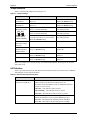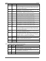
1
CoreModule™ 420
PC/104 Single Board Computer
Reference Manual
P/N 5001808A Revision A
Notice Page
NOTICE
No part of this document may be reproduced, transmitted, transcribed, stored in a retrieval system, or
translated into any language or computer language, in any form or by any means, electronic, mechanical,
magnetic, optical, chemical, manual, or otherwise, without the prior written permission of Ampro
Computers, Incorporated.
DISCLAIMER
Ampro Computers, Incorporated makes no representations or warranties with respect to the contents of
this manual or of the associated Ampro products, and specifically disclaims any implied warranties of
merchantability or fitness for any particular purpose. Ampro shall under no circumstances be liable for
incidental or consequential damages or related expenses resulting from the use of this product, even if it
has been notified of the possibility of such damages. Ampro reserves the right to revise this publication
from time to time without obligation to notify any person of such revisions. If errors are found, please
contact Ampro at the address listed below on the Notice page of this document.
TRADEMARKS
Ampro and the Ampro logo are registered trademarks, and CoreModule, EnCore, Little Board,
LittleBoard, MightyBoard, MiniModule, ReadyBoard, ReadyBox, ReadyPanel, and ReadySystem are
trademarks of Ampro Computers, Inc. All other marks are the property of their respective companies.
REVISION HISTORY
Revision
Reason for Change
Date
A, A
Initial Release
Jun/06
Ampro Computers, Incorporated
5215 Hellyer Avenue
San Jose, CA 95138-1007
Tel: 408 360-0200
Fax: 408 360-0222
www.ampro.com
© Copyright 2006, Ampro Computers, Incorporated
Audience Assumptions
This reference manual is for the person who designs computer related equipment, including but not
limited to hardware and software design and implementation of the same. Ampro Computers, Inc.
assumes you are qualified in designing and implementing your hardware designs and its related software
into your prototype computer equipment.
ii
Reference Manual
CoreModule 420
Contents
Chapter 1
About This Manual......................................................................................................... 1
Purpose of this Manual ...................................................................................................................... 1
Reference Material ............................................................................................................................. 1
Related Ampro Products .................................................................................................................... 2
Chapter 2 Product Overview ............................................................................................................... 5
PC/104 Architecture ........................................................................................................................... 5
Product Description ............................................................................................................................ 6
Module Features ............................................................................................................................ 6
Block Diagram................................................................................................................................ 9
Major Integrated Circuits (ICs) ..................................................................................................... 10
Connectors, Jumpers, and LEDs ..................................................................................................... 11
Connector Definitions................................................................................................................... 11
Jumper Definitions ....................................................................................................................... 12
LED Definitions ............................................................................................................................ 12
Specifications ................................................................................................................................... 14
Physical Specifications ................................................................................................................ 14
Mechanical Specifications............................................................................................................ 14
Power Specifications.................................................................................................................... 15
Environmental Specifications....................................................................................................... 15
Thermal/Cooling Requirements ................................................................................................... 15
Chapter 3 Hardware ........................................................................................................................... 17
Overview ....................................................................................................................................... 17
CPU (U14) ....................................................................................................................................... 18
Memory
....................................................................................................................................... 18
SDRAM Memory (U7, U8, U9, U10) ............................................................................................ 18
Flash Memory (U6) ...................................................................................................................... 18
Bytewide Socket (U5) .................................................................................................................. 18
Memory Map ................................................................................................................................ 18
Interrupt Channel Assignments.................................................................................................... 20
I/O Address Map .......................................................................................................................... 20
PC/104 Bus Interface (P1A,B,C,D) .................................................................................................. 22
IDE Interface (J6) ............................................................................................................................. 27
Compact Flash Socket Interface (J12)............................................................................................. 29
Floppy/Parallel Interface (J4) ........................................................................................................... 31
Floppy Disk Drive Port ................................................................................................................. 31
Parallel Port.................................................................................................................................. 31
Serial Interface (J3, J9, J13, J14) .................................................................................................... 33
USB Interface (J10).......................................................................................................................... 35
Utility Interface (J5) .......................................................................................................................... 36
Keyboard...................................................................................................................................... 36
Mouse ....................................................................................................................................... 36
Battery ....................................................................................................................................... 36
Reset Switch ................................................................................................................................ 36
Speaker ....................................................................................................................................... 36
Ethernet Interface (J2) ..................................................................................................................... 37
Video (LCD/CRT) Interface (J11)..................................................................................................... 38
CoreModule 420
Reference Manual
iii
Contents
Miscellaneous ...................................................................................................................................41
Real Time Clock (RTC) ................................................................................................................41
User GPIO Interface .....................................................................................................................41
Oops! Jumper (BIOS Recovery)...................................................................................................42
Serial Console ..............................................................................................................................42
Watchdog Timer ...........................................................................................................................43
Power Interface (J7) .........................................................................................................................44
Chapter 4 BIOS Setup ........................................................................................................................45
Introduction .......................................................................................................................................45
Accessing BIOS Setup (VGA Display) .........................................................................................45
Accessing BIOS Setup (Serial Console) ......................................................................................46
Main BIOS Setup Menu ....................................................................................................................47
BIOS Configuration Screen ..............................................................................................................48
Drive Configurations and Boot Options ........................................................................................48
User Interface Options..................................................................................................................50
Memory Control Options...............................................................................................................50
Power Management and Advanced User Options .......................................................................51
Video and On Board Controller Options.......................................................................................52
PCI, Plug n' Play, and Interrupt/DMA Assignments .....................................................................52
Splash Screen Customization...........................................................................................................55
Splash Screen Image Requirements............................................................................................55
Converting the Splash Screen File...............................................................................................55
On-Board Flash Access and Use .....................................................................................................57
Flash Programming Requirements...............................................................................................57
Building the Example....................................................................................................................57
Example Assumptions ..................................................................................................................58
Installing the Example Application................................................................................................58
Flash Boot API..............................................................................................................................58
Appendix A Technical Support .........................................................................................................59
Appendix B Connector Part Numbers..............................................................................................61
Index
........................................................................................................................................63
List of Figures
Figure 2-1. Stacking PC/104 Modules with the CoreModule 420......................................................5
Figure 2-2. Block Diagram .................................................................................................................9
Figure 2-3. Component Locations (Top View).................................................................................10
Figure 2-4. Connector Locations (Top View)...................................................................................11
Figure 2-5. Jumper and LED Locations (Top View) ........................................................................13
Figure 2-6. Connector Location (Bottom View) ...............................................................................13
Figure 2-7. Mechanical Dimensions (Top View)..............................................................................14
Figure 3-1. RS-485 Serial Port Implementation...............................................................................33
Figure 3-2. Oops! Jumper................................................................................................................42
Figure 3-3. Hot Cable Jumper .........................................................................................................42
Figure 4-1. BIOS Setup Opening Screen ........................................................................................47
Figure 4-2. BIOS Configuration Screen...........................................................................................48
iv
Reference Manual
CoreModule 420
Contents
List of Tables
Table 2-1. Major Integrated Circuit (Chips) Descriptions and Function .......................................... 10
Table 2-2. Connector Descriptions.................................................................................................. 11
Table 2-3. Jumper Settings ............................................................................................................. 12
Table 2-4. Ethernet Port (J2) LED Indicators.................................................................................. 12
Table 2-5. Weight and Footprint Dimensions.................................................................................. 14
Table 2-6. Power Supply Requirements ......................................................................................... 15
Table 2-7. Environmental Requirements ........................................................................................ 15
Table 3-1. Memory Map .................................................................................................................. 18
Table 3-2. Interrupt Channel Assignments ..................................................................................... 20
Table 3-3. DMA Map ....................................................................................................................... 20
Table 3-4. I/O Address Map ............................................................................................................ 20
Table 3-5. PC/104 Bus Interface Pin/Signal Descriptions (P1A) .................................................... 22
Table 3-6. PC/104 Bus Interface Pin/Signal Descriptions (P1B) .................................................... 23
Table 3-7. PC/104 Bus Interface Pin/Signal Descriptions (P1C) .................................................... 24
Table 3-8. PC/104 Bus Interface Pin/Signal Descriptions (P1D) .................................................... 25
Table 3-9. IDE Interface Pin/Signal Descriptions (J6)..................................................................... 27
Table 3-10. Compact Flash Socket Interface Pin/Signal Descriptions (J12) .................................. 29
Table 3-11. Floppy/Parallel Interface Pin/Signal Descriptions (J4)................................................. 31
Table 3-12. Serial Ports 1 & 2 Interface Pin/Signal Descriptions (J3, J9)....................................... 34
Table 3-13. Serial Ports 3 & 4 Interface Pin/Signal Descriptions (J13, J14)................................... 34
Table 3-14. USB Interface Pin/Signal Designations (J10) .............................................................. 35
Table 3-15. Utility Interface Pin/Signal Descriptions (J5)................................................................ 36
Table 3-16. Ethernet Interface Pin/Signal Descriptions (J2) ........................................................... 37
Table 3-17. Video Interface Pin/Signal Descriptions (J11) ............................................................. 39
Table 3-18. User GPIO Interface Pin/Signal Descriptions (J8)....................................................... 41
Table 3-19. Power Interface Pin/Signals (J7) ................................................................................. 44
Table 3-20. Power Interface Pin Arrangement (J7) ........................................................................ 44
Table 4-1. BIOS Setup Menus ........................................................................................................ 46
Table A-1. Technical Support Contact Information ......................................................................... 59
Table B-1. Connector and Manufacture’s Part Numbers ................................................................ 61
CoreModule 420
Reference Manual
v
Contents
vi
Reference Manual
CoreModule 420
Chapter 1 About This Manual
Purpose of this Manual
This manual is for designers of systems based on the CoreModule™ 420 PC/104 single board computer
(SBC) module. This manual contains information that permits designers to create an embedded system
based on specific design requirements.
Information provided in this reference manual includes:
• CoreModule 420 SBC Specifications
• Environmental requirements
• Major chips and features implemented
• CoreModule 420 SBC connector/pin numbers and definition
• BIOS Setup information
Information not provided in this reference manual includes:
• Detailed chip specifications
• Internal component operation
• Internal registers or signal operations
• Bus or signal timing for industry standard busses and signals
Reference Material
The following list of reference materials may be helpful for you to complete your custom design
successfully. Most of this reference material is also available on the Ampro web site in the Embedded
Design Resource Center. The Embedded Design Resource Center was created for embedded system
developers to share Ampro’s knowledge, insight, and expertise gained from years of experience.
Specifications
• PC/104 Specifications Revision 2.5, November 2003
For latest revision of the PC/104 specifications, contact the PC/104 Consortium, at:
Web site: http://www.pc104.org
Major Integrated Circuit (Chip) Specifications
The following chip specifications are used in the CoreModule 420 processor module:
• STMicroelectronics and the chip, STPC® Atlas, used for the embedded CPU
Web site: http://us.st.com/stonline/books/pdf/docs/7341.pdf
• Standard Microsystems Corp and the chip, FDC37B782, used for the Super I/O controller
Web site: http://www.smsc.com/main/catalog/fdc37b78x.html
• Intel Corporation and the chip, 82559ER, used for the Ethernet controller
Web site: http://www.intel.com/design/network/datashts/714682.htm (71468206.pdf)
CoreModule 420
Reference Manual
1
Chapter 1
About this Manual
NOTE
If you are unable to locate the datasheets using the links provided,
go to the manufacturer's web site where you can perform a search
using the chip datasheet number or name listed, including the
extension, (htm for web page, pdf for files name, etc.
Related Ampro Products
The following items are directly related to successfully using the Ampro product you have just
purchased or plan to purchase. Ampro highly recommends that you purchase and utilize a CoreModule
420 QuickStart Kit simultaneously with the design of your product.
CoreModule 420 Support Products
• CoreModule 420 QuickStart Kit (QSK)
The CoreModule 420 QuickStart Kit includes the CoreModule 420 CPU, a complete cable kit,
documentation, and drivers for Ampro supported operating systems and unique devices used on
the board.
• CoreModule 420 Documentation and Support Software CD-ROM
The CoreModule 420 Documentation and Support Software (Doc & SW) CD-ROM is provided
with the CoreModule 420 QuickStart Kit. The CD-ROM includes all of the CoreModule
documentation, including this Reference Manual and the CoreModule 420 QuickStart Guide in
PDF format, release notes, software utilities, and drivers.
Other CoreModule Products
• CoreModule™ 410 – This PC/104 embedded CPU is a state-of-the-art, high-integration x86based computer using STMicroelectronics 133 MHz STPC Elite processor, which provides a
complete embedded PC solution with most of the standard peripheral interfaces. In addition to
the standard CoreModule features (PC/104 form factor, PC/104 bus, +5 volt power, etc.), it
includes 16 MB soldered SDRAM memory, bytewide socket supporting DiskOnChip 2000
devices and a GPIO interface for customer usage. The CoreModule 410 also offers a watchdog
timer, serial console, BIOS extensions for OEM boot customization, and Advanced Power
Management.
• CoreModule™ 600 – This PC/104-Plus embedded single board computer (SBC) is a compact,
rugged, high integration, ultra low power 400 MHz ULV Celeron® processor with 256 kB of
internal cache, and all of the standard peripheral interfaces. In addition to the standard CoreModule
features (PC/104 form factor, PC/104-Plus, +5 volt power, etc.), the CoreModule 600 includes
10/100BaseT Ethernet, AGP 4X equivalent video with 32 MB video memory for CRT, TFT and
standard LCD flat panels, USB ports, RS-232C/RS-485 serial ports, and an onboard compact flash
socket, which supports up to 1 GB or more of memory. The CoreModule 600 also supports a
watchdog timer, serial console, battery-less boot, BIOS extensions for OEM boot customization,
some power management features and up to 256 MB of SDRAM memory.
• CoreModule™ 800 – This compact, rugged, high integration PCI-104 embedded single board
computer (SBC) provides the Intel® 855GME chipset to support the Intel 800 MHz Ultra Low
Voltage (ULV) Celeron M processor with 0 kB Level 2 internal cache, and all of the standard
peripheral interfaces. In addition to the standard CoreModule features (PCI-104 form factor, +5
volt power, etc.), the CoreModule 800 includes a Gigabit Ethernet port, 128-bit video with 64 MB
video memory for CRT, TFT and standard LCD flat panels, USB 2.0 ports (2), RS-232/RS-485
serial ports (2), and an onboard SODIMM socket, which supports up to 1 GB DDR memory. The
CoreModule 800 also supports a watchdog timer, serial console (remote access), battery-less boot,
and ACPI power management features.
2
Reference Manual
CoreModule 420
Chapter 1
About this Manual
Other Ampro Products
• ETX Family – These high-performance, compact, rugged Computer-on-Module (COM) solutions
use various x86 processors from Celeron to Pentium® M CPUs in an ETX Revision 2.7 form
factor to plug into your custom baseboard. Each ETX module provides standard peripherals,
including dual Ultra/DMA 33/66/100 IDE, floppy drive interface, PCI bus, ISA bus, serial,
parallel, PS/2 keyboard and mouse interfaces, 10/100BaseT Ethernet, USB ports, Video, and
AC’97 audio. A 50% thicker PCB, Ampro embedded BIOS extensions, such as watchdog timer,
battery-free boot, a customizable splash screen, BIOS recovery, serial console, and optional –
40°C to +85°C operation are available to meet your rugged application requirements.
• LittleBoard™ Family – These high-performance, highly integrated single board computers use
the EBX form factor (5.75"x8.00"), and are available with Pentium M, Celeron M, Pentium III, or
Celeron processors. The EBX-compliant LittleBoard single board computers offer functions
equivalent to a complete laptop or desktop PC system, plus several expansion cards. Built-in
extras to meet the critical requirements of embedded applications include onboard solid state disk
capability, watchdog timer, smart power monitor, and other embedded-PC BIOS enhancements.
• MightyBoard™ Family – These low-cost, high-performance single-board computers (SBC) use the
Mini-ITX form factor (6.75" x 6.75") and are available with Intel Celeron M and Pentium M
processors. MightyBoard products offer the equivalent functions of a complete laptop or desktop PC
system, including DDR memory, high performance graphics, USB 2.0, Gigabit Ethernet, plus
standard PCI expansion capability in one card slot. Ampro includes configuration control and
embedded BIOS extensions such as watchdog timer, battery-free boot, a customizable splash screen,
BIOS recovery, and serial console.
• MiniModule™ Family – This line of peripheral interface modules, compliant with PC/104, PC/104Plus, and/or PCI-104 form factor (3.6"x3.8") and standards, can be used with Ampro’s CoreModule,
LittleBoard, and ReadyBoard single board computers (SBCs) to expand the I/O configuration of
embedded systems. Ampro's highly reliable MiniModule products add value to existing designs by
adding I/O ports, such as IEEE 1394 (FireWire), or by adding support for legacy boards, such as a
PCI to ISA bridge adapter board.
• ReadyBoard™ Family – These low-cost, high-performance single-board computers (SBC) use the
EPIC form factor (4.5"x6.5") and are available with the Intel Celeron, Pentium III, Pentium M, and
Celeron M processors. ReadyBoard products offer functions equivalent to a complete laptop or
desktop PC system, plus several expansion cards, with PC-style connectors. Ampro includes
configuration control and embedded BIOS extension such as watchdog timer, battery-free boot, a
customizable splash screen, BIOS recovery, and serial console.
• ReadyPanel™ Family – This is a series of high performance, low cost, turnkey systems incorporating
an LCD and a touch screen for a Human Machine Interface solution. All ReadyPanels come with
one of Ampro's versatile ReadyBoard models in a variety of touch screen sizes pre-loaded with one
of Ampro's supported operating systems (Windows® CE, etc.). The ReadyPanel includes a compact
flash socket, a specific size of SODIMM memory, an Ethernet port, two serial ports, two USB ports
standard, with two additional USB ports on selected models. The current models are driven by an
integrated 4-wire resistive 6.5" touch screen that displays up to 262k colors. The ReadyPanel is
powered by +5V (for board) and +12V DC (for panel) power input.
CoreModule 420
Reference Manual
3
Chapter 1
About this Manual
• ReadySystem™ Family – The ReadySystem family is a series of high performance, low cost
turnkey systems that come with a ReadyBoard product installed into a particular size ReadyBox
enclosure with a specific size SODIMM, and a 2 ½" hard disk drive pre-loaded with one of
Ampro's supported operating systems (Linux®, etc.). The ReadySystem provides all of the
ReadyBoard's standard PC style connectors accessible on the front I/O panel, including three
audio connectors, and a slot for a compact flash card. Depending on the enclosure, you may add
PC style connectors for two additional serial ports (4 total), two additional USB ports (4 total),
and one parallel port connector. You may also install up to two PCI-104 or PC/104-Plus
expansion boards into the ReadySystem ATX and 2U enclosures. A ReadySystem comes pretested and ready for application loading to provide customers with the fastest possible
deployment of their embedded applications. Refer to the specific ReadySystem Users Guide on
the web site, or the ReadyBoard product Documentation and Support Software (Doc & SW)
CD-ROM for more information.
4
Reference Manual
CoreModule 420
Chapter 2
Product Overview
This introduction presents general information about the PC/104 architecture and the CoreModule 420
single board computer (SBC). After reading this chapter you should understand:
• PC/104 Concept
• CoreModule 420 architecture
• CoreModule 420 features
• Major components
• Connectors
• Specifications
PC/104 Architecture
The PC/104 architecture affords a great deal of flexibility in system design. You can build a simple
system using only a CoreModule single board computer (SBC), with input/output devices connected to
its serial or parallel ports, and a solid state disk on chip in the bytewide socket or a compact flash card in
the compact flash socket. To expand a simple CoreModule system, simply add self-stacking Ampro
MiniModules or 3rd party PC/104 expansion boards to provide additional capabilities, such as:
• Additional I/O ports (such as IEEE 1394 (FireWire)
• Analog or digital I/O interfaces
PC/104 expansion modules can be stacked with the CoreModule 420 avoiding the need for card cages
and backplanes. The PC/104 expansion modules can be mounted directly to the PC/104 bus connector
of the CoreModule 420. PC/104-compliant modules can be stacked with an inter-board spacing of
~0.66" (16.7 mm) so that a 3-module system fits in a 3.6" x 3.8" x 2.4" space. See Figure 2-1.
One or more MiniModule products or other PC/104 modules can be installed on the CoreModule
expansion connectors. When installed on the PC/104 headers, the expansion modules fit within the
CoreModule outline dimensions. Most MiniModule products have stack through connectors compatible
with the PC/104 Version 2.5 specification. Several modules can be stacked on the CoreModule headers.
Each additional module increases the thickness of the package by 0.60" (15 mm). See Figure 2-1.
PC/104 Module
4-40 nut (4)
0.6 inch spacer (4)
CoreModule 420
PC/104 Module
Stackthrough
Expansion
Bus Headers
0.6 inch spacer (4)
CM420stack
PC/104 Module
4-40 screw (4)
Figure 2-1. Stacking PC/104 Modules with the CoreModule 420
CoreModule 420
Reference Manual
5
Chapter 2
Product Overview
Product Description
The CoreModule 420 SBC is an exceptionally high integration, high-performance, 486-based PC
compatible system in the PC/104 form factor. This rugged and high quality single board system contains
all the component subsystems of a PC/AT motherboard plus the equivalent of several PC/AT expansion
boards.
In addition, the CoreModule 420 SBC includes a comprehensive set of system extensions and
enhancements that are specifically designed for embedded systems. These enhancements ensure failsafe embedded system operation, such as, a watchdog timer. It is designed to meet the size, power
consumption, temperature range, quality, and reliability demands of embedded applications. The
CoreModule 420 requires a single +5V power source.
The CoreModule 420 SBC is particularly well suited to either embedded or portable applications. Its
flexibility makes system design quick and easy. It can be stacked with Ampro MiniModules or other
PC/104-compliant expansion board, or it can be used as the computing engine in a fully customized
application.
Module Features
• CPU
♦
Provides 133 MHz x86 based STPC ATLAS microprocessor
♦
Fully supports PC compatible architecture
♦
Provides 8 kB Unified Instruction and Data Cache
♦
Provides Parallel Processing Integrated Floating Point Unit
♦
Provides Low Power and System Management Modes
• Memory
♦
Provides 64 MB standard SDRAM (soldered on the board)
♦
Supports 100 MHz Clock Speed
♦
Provides 32-pin bytewide memory socket
•
♦
Supports a DiskOnChip® device
1 MB Flash memory
•
Stores system BIOS
•
Stores system Setup parameters and manufacturing information
•
Supports battery-free boot capability
•
768 kB available for OEM use
• PC/104 Bus Interface
♦
Supports clock speeds up to 8.25 MHz
• IDE Interface
6
♦
Supports two enhanced IDE devices
♦
Provides Fast ATA-capable interface for high-speed PIO modes
(PIO modes 0 to 4)
♦
Supports ATAPI and DVD peripherals
♦
Supports IDE native and ATA compatibility modes
Reference Manual
CoreModule 420
Chapter 2
Product Overview
• Compact Flash Socket
♦
Provides compact flash socket (Type I or II)
♦
Supports IDE compact flash cards
♦
Attached to Secondary IDE bus
• Floppy Disk Controller
♦
Provides shared floppy/parallel port connector
♦
Supports two floppy drives
♦
Supports all standard PC/AT formats: 360 kB, 1.2 MB, 720 kB, 1.44 MB, 2.88 MB
• Serial Ports
♦
Provides four buffered RS-232 serial ports with full handshaking and modem capability
♦
Provides 16550 (or 16540-equivalent) UARTs, each with a built-in 16-byte FIFO buffer
♦
Supports RS-232 or RS-485 operation on ports 1 and 2
♦
Supports programmable word length, stop bits, and parity
♦
Supports 16-bit programmable baud-rate generator and a interrupt generator
• Parallel Port
♦
Provides shared parallel/floppy port connector
♦
Supports standard printer port
♦
Supports IEEE standard 1284 protocols, including EPP, ECP modes
♦
Provides bidirectional data lines
♦
Supports 16 byte FIFO for ECP mode
• Ethernet Controller
♦
Intel 82559ER Controller chip
♦
Supports IEEE 802.3 10BaseT/100BaseT compatible physical layer
♦
Supports Auto-negotiation for speed, duplex mode, and flow control
♦
Supports full duplex or half-duplex mode
•
Full-duplex mode supports transmit and receive frames simultaneously
•
Supports IEEE 802.3x Flow control in full duplex mode
•
Half-duplex mode supports enhanced proprietary collision reduction mode
• Utility Interface
♦
Keyboard and PS/2 Mouse Interface
♦
Supports external battery for Real Time Clock operation
♦
Supports standard external 8Ω speaker interface
♦
Supports external reset switch
• USB Ports
♦
Provides one root USB hub
♦
Provides one USB port
♦
Supports USB v1.1 and Universal OHCI v1.1
CoreModule 420
Reference Manual
7
Chapter 2
Product Overview
• Video (LCD/CRT) Display
Enhanced 2D graphics controller
♦
Supports BitBLT implementation for all 256 raster operations for Windows® support
♦
Supports all BLT transparency modes
•
Bitmap transparency
•
Pattern transparency
•
Source transparency
•
Destination transparency
♦
Supports 8, 16, 24, and 32-bit pixel depths
♦
Supports hardware clipping
♦
Supports fast line draw engine with anti-aliasing
♦
Supports fast triangle fill engine
♦
Supports 4-bit alpha blend font for anti-aliased text display
♦
Supports 64-bit wide pipelined architecture operating at 100 MHz
♦
Supports complete double buffered registers for pipelined operation
♦
Provides video memory up to 4 MB – selected in BIOS Setup
CRT Interface
♦
VGA Controller with 135 MHz triple RAMDACs for 1280 x 1024 x 75 Hz display
♦
Supports 24-bit pixel depth
♦
Interlaced or non-interlaced output
LCD/TFT Interface
♦
Supports VESA Flat Panel Display interface FPDI-1B
♦
Supports programmable panel size up to 1024x768 pixel display resolution
♦
Supports VGA and SVGA active matrix TFT flat panels
♦
Support internal CRT controller for display mode settings
♦
Supports 9-, 12-, and 18-bit interface (1 Pixel/Clock)
♦
Supports 2x9-bit interface (2 Pixels/Clock)
♦
Supports programmable image position
♦
Supports 3.3V or 5V LCD panels; jumper selectable
♦
Provides Video BIOS customization tools
• Miscellaneous
8
♦
Provides Real Time Clock and CMOS RAM, with support for battery-free operation
♦
Provides General Purpose I/O (GPIO) interface
♦
Supports Oops! Jumper (BIOS Recovery)
♦
Supports Serial Console (Console Redirection)
♦
Supports customizable Splash Screen
♦
Supports Watchdog Timer (WDT)
Reference Manual
CoreModule 420
Chapter 2
Product Overview
Block Diagram
Figure 2-2 shows the functional components of the module.
Memory
(SDRAM)
Video (CRT/TFT)
Internal PCI
Bus
CPU
Core
STPC Atlas
(Computer
in a Chip)
Ethernet
Controller
I2C Interface
USB Port
Speaker
Serial Ports
(Serial 1 & 2)
HostPeripheral
Interface
GPIOs (8)
IDE Devices
(HDD, Compact Flash,
CD-ROM, etc. )
PC/104 Interface
ISA Bus
Bytewide
Socket
BIOS
CM420blkdiag
Floppy Drive
RTC
Parallel Port
Super I/O
Controller
Serial Ports
(Serial 3 & 4)
Utility Interface
(Keyboard, Mouse,
External Bat. etc)
Figure 2-2. Block Diagram
CoreModule 420
Reference Manual
9
Chapter 2
Product Overview
Major Integrated Circuits (ICs)
Table 2-1 lists the major integrated circuits (ICs or chips), including a brief description of each, on the
CoreModule 420 and Figure 2-3 shows the location of the major chips.
Table 2-1. Major Integrated Circuit (Chips) Descriptions and Function
Chip Type
CPU (U14)
Mfg.
STMicroelectronics
Model
STPC
ATLAS
Description
Embedded CPU – The combination of
features in the CPU provide more than
just a processor. It also provides a
graphics controller, PCI controller,
EIDE controller, I/O features, and
power management capabilities.
Function
Embedded
CPU
Super I/O
Controller
(U13)
Standard
Microsystems
Corp.
FDC37B782
Super I/O – This chip provides serial
and Floppy controllers
Floppy/Serial
Controllers
Ethernet
Controller
(U15)
Intel
82559ER
Ethernet – This chip provides the
10/100BaseT Ethernet function.
Ethernet
2
1
JP6
J14
9
10
2
J3
1
3
J13
JP5 JP4
J4
1
J8
2
JP8
U7
U35
U3
JP9
U12
U36
JP7
L5
J11
4
10
D8
J9
JP1
J5
U8
U9
U10
U6
U11
CPU (U14)
Flash
Memory (U6)
U41
U40
Bytewide
Socket (U5)
U5
D1
U14
Super I/O (U13)
D2
J2
U15
SDRAM
Memory
(U7-U10)
U13
Ethernet
Controller (U15)
J10
U16
Ethernet
Magnetics (U16)
J7
JP2
P1
CM420RFM_01a
Figure 2-3. Component Locations (Top View)
NOTE
10
Pin-1 is shown as black pin (square or round) in connectors
and jumpers in all illustrations, except where noted.
Reference Manual
CoreModule 420
Chapter 2
Product Overview
Connectors, Jumpers, and LEDs
Connector Definitions
Table 2-2 describes the connectors shown in Figures 2-4 to 2-6. Refer to Appendix B for part numbers.
Table 2-2. Connector Descriptions
Jack/Plug #
Access
Description
P1A/1B & P1C/1D –
Top/
PC/104 Bus Bottom
104-pin, 0.1", connectors used for PC/104 (ISA) bus
J2 – Ethernet
Top
8-pin, 0.1", connector used for the Ethernet interface
J3 – Serial 1 (COM1)
Top
10-pin, 0.1", connector used for the Serial 1 interface
J4 – Floppy/Parallel
Top
26-pin, 0.1", connector provides the Floppy/Parallel interface
J5 – Utility
Top
10-pin, 0.1", connector used for the Utility interface
J6 – IDE
Top
44-pin, 2 mm connector used for the IDE interface
J7 – Power
Top
10-pin, 0.1", connector used for the Power connection
J8 – GPIO (User)
Top
10-pin, 2 mm connector used for the User defined GPIO signals
J9 – Serial 2 (COM2)
Top
10-pin, 0.1", connector used for the Serial 2 interface
J10 – USB
Top
5-pin, 0.1", connector used for the USB interface
J11 – Video
Top
44-pin, 2 mm connector used for the LCD/CRT interface
J12 – Compact Flash
Bottom
50-pin, 1.27 mm, socket used for compact flash cards
J13 – Serial 3 (COM3)
Top
10-pin, 0.1", connector used for the Serial 3 interface
J14 – Serial 4 (COM4)
Top
10-pin, 0.1", connector used for the Serial 4 interface
Utility (J5)
IDE (J6)
2
J5
1
Serial 4 (J14)
(COM 4)
JP6
J14
9
10
J13
J3
1
U7
Serial 3 (J13)
(COM 3)
J4
1
J8
2
JP8
U8
U9
Serial 1 (J3)
(COM 1)
JP5 JP4
U35
U36
U3
JP9
U12
J11
2
3
JP7
L5
J9
4
10
D8
Serial 2 (J9)
(COM 2)
JP1
GPIO (J8)
U10
U6
U11
U40
Video (J11)
U41
Floppy/Parallel (J4)
U5
D1
U14
D2
J2
U15
Ethernet (J2)
U13
U16
P1B
P1A
USB (J10)
J7
Power (J7)
JP2
P1
P1C
P1D
(PC104 Bus)
CM420RFM_01b
J10
Figure 2-4. Connector Locations (Top View)
CoreModule 420
Reference Manual
11
Chapter 2
Product Overview
Jumper Definitions
Table 2-3 describes the jumpers shown in Figure 2-5.
Table 2-3. Jumper Settings
Jumper #
Installed
Removed/Installed
JP1 Serial Port 2
Termination
Enable RS-485 Termination
(Pins 1-2)
Disable RS-485 Termination
(Removed) Default setting
JP2 Serial Port 1
Termination
Enable RS-485 Termination
(Pins 1-2)
Disable RS-485 Termination
(Removed) Default setting
JP4 & JP5
BIOS/DOC Select
JP5 JP4
Enable Internal BIOS – Normal operation,
(Pins 1-3 on both JP4 & JP5)
Disabled – Won’t Boot
(See other positions)
Enable External BIOS – Used for recovery
(Pins 1-2 on both JP4 & JP5)
Disabled – Won’t Boot
(See other positions)
BIOS/DOC Select
Jumper Setting
(Shown in Default)
Enable DOC – Boot from DiskOnChip in
bytewide socket (Pins 1-3 & 2-4 on both
JP4 & JP5) Default setting
Disabled – Won’t Boot
(See other positions)
JP6
Flat Panel Voltage
Selection
+3.3 Volts (Pins 1-2) Default setting
+5 Volts (Pins 2-3)
JP7
DiskOnChip Boot
Address Select
Access from DC000h-DDFFFh
(Pins 1-2) Default setting
Access from CC000h-CDFFFh
(Removed)
JP8 Serial Port 1
Enable Serial Port 1
(Pins 1-2) Default setting
Disabled Serial Port 1
(Pins 2-3)
JP9 Serial Port 2
Enable Serial Port 2
(Pins 1-2) Default setting
Disabled Serial Port 2
(Pins 2-3)
4
3
24
1
2
1
Notes: The jumpers use 2 mm pin spacing. JP8 and JP9 Enable/Disable the Serial ports at the STPC
Altas CPU (U14).
LED Definitions
Table 2-4 provides the LED color and definitions for the Ethernet Port (J2) located on the CoreModule
420 and Figure 2-5 provides the locations.
Table 2-4. Ethernet Port (J2) LED Indicators
Indicator
Definition
Ethernet
Link/Activity LED (D1)
Link/Activity LED – This yellow LED is the link/ activity
indicator and provides the status of Ethernet port (J2).
The Link/Activity LED indicates a link is established with either
transmit or receive activity.
Yellow On – This indicates a link is present.
Yellow Flashing – This indicates activity is present.
Yellow Off – This indicates no link or activity is present.
Ethernet Speed (D2)
Speed LED – This green LED is the LAN Speed indictor and
indicates the transmit or receive speed of Ethernet port (J2).
Green On – This indicates the operating speed is 100 Mbps
Green Off – This indicates the operating speed is 10 Mbps.
12
Reference Manual
CoreModule 420
Chapter 2
Product Overview
JP6
JP7
JP9
JP8
JP1
JP4
JP5
2
JP1
J5
1
JP6
J14
9
10
J3
JP5 JP4
U35
U3
JP9
U12
U36
JP7
L5
J4
1
J8
JP8
U7
2
U9
U8
U10
U41
U40
Bytewide
Socket (U5)
Pin-1
U6
U11
U5
D1
D2
U14
J2
U15
Link/Activity
LED (D1)
Speed
LED (D2)
U13
J10
U16
J7
JP2
JP2
P1
CM420RFM_01c
J11
2
1
3
J13
D8
J9
4
10
Figure 2-5. Jumper and LED Locations (Top View)
Compact Flash
Socket (J12)
D3
D4
Voltage
Regulator
(U19)
U19
U37
U1
U21
D5
U22
U20
U42
U24
U23
F1
USB Fuse (F1)
PC/104 Bus (P1)
CM420RFM_02a
U30
U28
Y2
Y3
U27
Y1
U38
U29
U25
J12
Figure 2-6. Connector Location (Bottom View)
CoreModule 420
Reference Manual
13
Chapter 2
Product Overview
Specifications
Physical Specifications
Table 2-5 gives the physical dimensions of the module and Figure 2-7 gives the mounting dimensions.
Table 2-5. Weight and Footprint Dimensions
Item
Dimension
Weight
Height (upper surface)
0.0925 kg. (0.204 lbs.)
10.99 mm (0.43")
See also Note on page 15.
Width
90.2 mm (3.6")
Length
95.9 mm (3.8")
NOTE
Height is measured from the
upper board surface to the
highest permanent
component (PC/104
connector) on the upper
board surface. This does
not include the heatsink.
3.575
3.431
3.375
3.050
3.155
2.375
2.100
JP1
JP6
J6
9
10
3.281
2.890
1.800
1.160
0.400
0.150
0.000
Mechanical Specifications
10
J9
J14
J13
4
2
3
1
3.400
3.375
J5
JP5 JP4
3.195
J3
JP7
JP8
JP9
3.100
2.500
1
J8
2
2.580
J11
CM420RFM_01d
J4
CPU
U14
0.940
P1B
P1A
P1C
P1D
0.700
J10
J2
0.394
0.300
0.000
3.112
0.850
0.280
-0.200
-0.030
-0.020
0.000
0.050
3.350
JP2
J7
3.150
0.000
-0.010
-0.200
Figure 2-7. Mechanical Dimensions (Top View)
NOTE
14
All dimensions are given in inches. Pin-1 is shown as a black or white pin
(square or round) in connectors and jumpers in this illustration.
Reference Manual
CoreModule 420
Chapter 2
Product Overview
NOTE
The CoreModule 420 is in violation of the PC/104 height limitations in two
places on the bottom of the board. The voltage regulator (U19) exceeds the
allowed height limitation by 0.085 inches and the compact flash socket (J12)
exceeds the height limitation by 0.2 inches. See Figure 2-6.
Power Specifications
Table 2-6 provides the power requirements.
Table 2-6. Power Supply Requirements
Parameter
Characteristics
Input Type
Regulated DC voltages
In-rush* Current
+5 VDC +/- 5% @ 13.72 Amps
BIT** Current
(Typical)
+5 VDC +/- 5% @ 1.51 Amps (7.56W)
Notes: *In-rush measured with video, 64 MB memory (fixed), and power connected. Typically, in-rush
current reflects the short duration current spike associated with charging large on-board bulk capacitance
during power supply start up. However, the in-rush current value is the result of placing a switch on the
DC output of a fully 'ramped' power supply to give a worst-case current value, which is much higher
than the standard method. This in-rush value should be regarded as a maximum design guideline, not a
requisite or typical value.
**The average BIT (burn in test) current is conducted with 64 MB memory (fixed), a floppy disk drive
(FDD), a IDE hard disk drive (HDD), keyboard, mouse, serial loopbacks (4), externally connected USB
HDD (1), and active Ethernet channel (1) in a Windows® 2000 operating system (OS) environment.
Environmental Specifications
Table 2-7 provides the operating and storage condition ranges required for this module.
Table 2-7. Environmental Requirements
Parameter
Conditions
Temperature
Operating
-20° to +70° C (-4° to 158° F)
Extended (Optional)
–40° to +85° C (–40° F to +185° F)
Storage
–55° to +85° C (–67° F to +185° F)
Humidity
Operating
20% to 80% relative humidity, non-condensing
Non-operating
5% to 95% relative humidity, non-condensing
Thermal/Cooling Requirements
The CPU, Super I/O, and voltage regulator are the sources of heat on the board. The CoreModule 420 is
designed to operate at its maximum CPU speed of 133 MHz and requires a heatsink (provided).
CoreModule 420
Reference Manual
15
Chapter 2
16
Product Overview
Reference Manual
CoreModule 420
Chapter 3
Hardware
Overview
This chapter discusses the chips and connectors of the module features in the following order:
• CPU (U14)
• Memory
♦
SDRAM (U7, U8, U9, U10)
♦
Flash Memory (U6)
♦
Bytewide socket (U5)
• PC/104 (P1A, B, C, D)
• IDE (J6)
• Compact flash socket (J12)
• Serial (J3, J9, J13, J14)
• Floppy/Parallel (J4)
• Utility (J5)
♦
Keyboard
♦
Mouse
♦
Battery
♦
Reset Switch
♦
Speaker
• Ethernet (J2)
• USB (J10)
• Video (J11)
• Miscellaneous
♦
Time of Day/RTC
♦
User GPIO (J8)
♦
Oops! Jumper (BIOS Recovery)
♦
Watchdog timer
• Power (J7)
NOTE
CoreModule 420
Ampro Computers, Inc. only supports the features/options tested and listed in this
manual. The main integrated circuits (chips) used in the CoreModule 420 may
provide more features or options than are listed for the CoreModule 420, but some
of these features/options are not supported on the module and will not function as
specified in the chip documentation.
Reference Manual
17
Chapter 3
Hardware
CPU (U14)
The CoreModule 420 uses an embedded microprocessor operating at 133 MHz, that combines a
powerful x86 core and a selection of peripheral interfaces into one chip. The STPC Atlas integrates a
standard 5th generation x86 core. It supports logic including PC/104, EIDE controllers and combines
these with standard I/O interfaces to provide a PC compatible subsystem in a single chip.
Memory
The CoreModule 420 memory (storage) consists of the following elements:
• SDRAM
• Flash memory
• Bytewide socket
SDRAM Memory (U7, U8, U9, U10)
The CoreModule 420 contains four 16-bit SDRAM chips of 16 MB each for a total of 64 MB memory
soldered into place on the module and operating at 100 MHz.
Flash Memory (U6)
A 1 MB flash device is used for system BIOS on the module and 768 kB is available for user code. The
Flash memory also stores system parameters (CMOS settings) and can be used for battery-less boot
capability when no battery is available.
Bytewide Socket (U5)
The CoreModule 420 has a 32-pin DIP socket on the module used as a bytewide socket. This socket
supports DiskOnChip devices.
A memory device installed in the bytewide socket can be used for:
• DOC2000 (M-Systems DiskOnChip©)
• External BIOS (BIOS recovery)
Memory Map
Table 3-1. Memory Map
Address
1 0000 0000
Size
Use
256 kB
Flash ROM (BIOS)
FFFC 0000
130,560 kB
Unused
F804 0000
128 kB
Ethernet
F802 0000
120 kB
Unused
F800 2000
4 kB
Ethernet
F800 1000
4 kB
USB
F800 0000
3824 MB
0900 0000
16 MB
STPC Graphics Memory
0800 0000
64 MB
Unused
Unused
Memory Map Table continued on next page
18
Reference Manual
CoreModule 420
Chapter 3
Hardware
Table 3-1. Memory Map (continued)
Address
Size
Use
0400 0000
1 MB
RAM or Unused if Framebuffer is set to 1 MB or more
03F0 0000
1 MB
RAM or Unused if Framebuffer is set to 2 MB or more
03E0 0000
1 MB
RAM or Unused if Framebuffer is set to 3 MB or more
03D0 0000
1 MB
RAM or Unused if Framebuffer is set to 4 MB
03C0 0000
44 MB
RAM
Use
Address
Size
Memory hole size selected
8 MB
4 MB
2 MB
1 MB
0 MB
0100 0000
1 MB
H
H
H
H
R
00F0 0000
1 MB
H
H
H
R
R
00E0 0000
1 MB
H
H
R
R
R
00D0 0000
1 MB
H
H
R
R
R
00C0 0000
1 MB
H
R
R
R
R
00B0 0000
1 MB
H
R
R
R
R
00A0 0000
1 MB
H
R
R
R
R
0090 0000
1 MB
H
R
R
R
R
R = RAM
H = Memory Hole, forwarded to ISA
The board can be configured to have access to the 1 MB
Flash anywhere in the memory hole, on 1 MB alignment.
Address
Size
Use
0080 0000
7 MB
0010 0000
128 kB
000E 0000
8 kB
Unused
000D E000
8 kB
DiskOnChip, if DC000-DDFFF window selected.
Unused if no DOC present.
000D C000
56 kB
Unused
000C E000
8 kB
DiskOnChip, if CC000-CDFFF window selected.
Unused if no DOC present.
000C C000
48 kB
Unused
000C 0000
128 kB
Unused, reserved for Video RAM, or
in SMI mode, mapped to RAM
000A 0000 0000 0000
640 kB
Base memory
CoreModule 420
RAM
Shadowed BIOS
Reference Manual
19
Chapter 3
Hardware
Interrupt Channel Assignments
The channel interrupt assignments are shown in Table 3-2.
Table 3-2. Interrupt Channel Assignments
Device vs
IRQ No.
0
Timer
X
Keyboard
1
2
3
4
5
6
7
8
9
10 11
12
13
14
15
Disable
X
Secondary
Cascade
X
COM1
X
Z
COM2
X
Z
COM3
O
O
O
O
O
O
O
D
O
O
Z
COM4
O
O
O
O
O
O
D
O
O
O
Z
O
O
O
O
Z
Floppy
X
O
Parallel
O
O
O
D
RTC
X
Prim. IDE
D
Z
Sec. IDE
D
Z
USB
O
O
O
O
O
O
O
O
D
O
Z
Ethernet
O
O
D
O
O
O
O
O
O
O
Z
Math
Coprocessor
X
O
PS/2 Mouse
O
O
O
O
O
O
O
D
Z
Legend: D = Default, O = Optional, X = Fixed, Z = Disable option
NOTE
The devices listed with a “Z” in the Disable column indicate the device
can be disabled, which will free the IRQ for another device.
Table 3-3. DMA Map
DMA #
Use
0-1, 5, 6, 7
Direct Memory Access
2
Floppy (configurable)
3
LPT 1, only in ECP mode (configurable)
4
DMA 1 cascade
I/O Address Map
Table 3-4. I/O Address Map
20
Address (hex)
Subsystem
0000-000F
Primary DMA Controller (#1)
0020-0021
Master Interrupt Controller (#1)
0022-0023
STPC Configuration
Reference Manual
CoreModule 420
Chapter 3
Hardware
Address (hex)
Subsystem
0040-0043
Programmable Interrupt Timer (Clock/Timer)
0060-0064
0070-0071
Keyboard Controller
0080-008F
DMA Page
0094
RTC/ NMI enable
Motherboard VGA enable
00A0-00A1
Slave Interrupt Controller (#2)
00C0-00DF
Secondary DMA Controller (#2)
0102
VGA setup register
01F0-01F7
Primary IDE (configurable)
0170-0177
Secondary IDE (configurable)
0201
02E8-02EF
Watchdog trigger (configurable, disabled by default)
COM4 (configurable)
02F8-02FF
COM2 (configurable)
0376
0378-037B
Secondary IDE (see 170)
LPT 1 (configurable, disabled by default)
0378-037F
LPT 1 (only in EPP modes)
03B4-03B5
VGA registers (monochrome mode only)
03BA
VGA registers (monochrome mode only)
03C0-03CF
VGA registers
03D4-03D5
VGA registers (color mode only)
03DA
VGA registers (color mode only)
03E8-03EF
COM3 (configurable)
03F0-03F1
Super I/O Configuration
03F0-03F5, 03F7
Floppy Disk Controller (configurable)
03F6
Primary IDE (see 1F0)
03F8-03FF
COM1 (configurable)
0778-077A
LPT 1 (only in ECP modes)
0CF8
0CFC-0CFF
46E8
PCI Configuration Address
PCI Configuration Data
VGA add-in mode enable register
D000-D007
General Purpose I/O for customer use
D400-D407
Board control
E400-E43F
On-Board Ethernet
E800-E80F
IDE Bus Master registers (PCI mode)
EC00-EC0F
Secondary IDE Control (PCI mode)
F000-F00F
Secondary IDE Command (PCI mode)
F400-F40F
Primary IDE Control (PCI mode)
F800-F80F
Primary IDE Command (PCI mode)
Note: Configurable indicates the device’s base address can be configured and/or
the device can be disabled, either through BIOS Setup or hardware jumpers.
CoreModule 420
Reference Manual
21
Chapter 3
Hardware
PC/104 Bus Interface (P1A,B,C,D)
The PC/104 Bus uses a 104-pin 0.1" connector interface. This interface connector will carry all of the
appropriate PC/104 signals operating at clock speeds to 8.25 MHz. This interface connector is located
on both the top and bottom of the module.
Table 3-5. PC/104 Bus Interface Pin/Signal Descriptions (P1A)
22
Pin #
Signal
Description (P1 Row A)
1 (A1)
IOCHCHK* I/O Channel Check – This signal may be activated by ISA boards to
request that a non-maskable interrupt (NMI) be generated to the system
processor. It is driven active to indicate an uncorrectable error has been
detected.
2 (A2)
SD7
System Data 7 – This signal (0 to 19) provides a system data bit.
3 (A3)
SD6
System Data 6 – Refer to SD7, pin A2, for more information.
4 (A4)
SD5
System Data 5 – Refer to SD7, pin A2, for more information.
5 (A5)
SD4
System Data 4 – Refer to SD7, pin A2, for more information.
6 (A6)
SD3
System Data 3 – Refer to SD7, pin A2, for more information.
7 (A7)
SD2
System Data 2 – Refer to SD7, pin A2, for more information.
8 (A8)
SD1
System Data 1 – Refer to SD7, pin A2, for more information.
9 (A9)
SD0
System Data 0 – Refer to SD7, pin A2, for more information.
10 (A10)
IOCHRDY
I/O Channel Ready – This signal allows slower ISA boards to lengthen
I/O or memory cycles by inserting wait states. This signal’s normal state
is active high (ready). ISA boards drive the signal inactive low (not
ready) to insert wait states. Devices using this signal to insert wait states
should drive it low immediately after detecting a valid address decode and
an active read, or write command. The signal is released high when the
device is ready to complete the cycle.
11 (A11)
AEN
Address Enable – This signal is reserved for the ISA Bus and is asserted
during DMA cycles to prevent I/O slaves from misinterpreting DMA
cycles as valid I/O cycles.
12 (A12)
SA19
System Address 19 – These signals (0 to 19) provide system address bits.
13 (A13)
SA18
System Address 18 – Refer to SA19, pin A12, for more information.
14 (A14)
SA17
System Address 17 – Refer to SA19, pin A12, for more information.
15 (A15)
SA16
System Address 16 – Refer to SA19, pin A12, for more information.
16 (A16)
SA15
System Address 15 – Refer to SA19, pin A12, for more information.
17 (A17)
SA14
System Address 14 – Refer to SA19, pin A12, for more information.
18 (A18)
SA13
System Address 13 – Refer to SA19, pin A12, for more information.
19 (A19)
SA12
System Address 12– Refer to SA19, pin A12, for more information.
20 (A20)
SA11
System Address 11 – Refer to SA19, pin A12, for more information.
21 (A21)
SA10
System Address 10 – Refer to SA19, pin A12, for more information.
22 (A22)
SA9
System Address 9 – Refer to SA19, pin A12, for more information.
23 (A23)
SA8
System Address 8 – Refer to SA19, pin A12, for more information.
24 (A24)
SA7
System Address 7 – Refer to SA19, pin A12, for more information.
25 (A25)
SA6
System Address 6 – Refer to SA19, pin A12, for more information.
26 (A26)
SA5
System Address 5 – Refer to SA19, pin A12, for more information.
Reference Manual
CoreModule 420
Chapter 3
Hardware
Pin #
Signal
Description (P1 Row A)
27 (A27)
SA4
System Address 4 – Refer to SA19, pin A12, for more information.
28 (A28)
SA3
System Address 3 – Refer to SA19, pin A12, for more information.
29 (A29)
SA2
System Address 2 – Refer to SA19, pin A12, for more information.
30 (A30)
SA1
System Address 1 – Refer to SA19, pin A12, for more information.
31 (A31)
SA0
System Address 0 – Refer to SA19, pin A12, for more information.
32 (A32)
GND
Ground
Notes: The shaded area denotes power or ground. The signals marked with * indicate active low.
Table 3-6. PC/104 Bus Interface Pin/Signal Descriptions (P1B)
Pin #
Signal
Description (P1 Row B)
33 (B1)
GND
Ground
34 (B2)
RstDrv
Reset Drive – This signal is used to reset or initialize system logic on
power up or subsequent system reset.
35 (B3)
+5V
+5V power ±5%
36 (B4)
IRQ9
Interrupt Request 9 – Asserted by a device when it has pending interrupt
request. Only one device may use this request line at a time.
37 (B5)
NC
Not connected (-5 volts)
38 (B6)
DRQ2
DMA Request 2 – Used by I/O resources to request DMA service, or to
request ownership of the bus as a bus master device. Must be held high
until associated DACK2 line is active.
39 (B7)
NC
Not connected (-12 volts)
40 (B8)
ZWS*
Zero Wait State – This signal is driven low by a bus slave device to
indicate it is capable of performing a bus cycle without inserting any
additional wait states. To perform a 16-bit memory cycle without wait
states, this signal is derived from an address decode.
41 (B9)
+12V
+12 Volts
42 (B10)
Key (NC)
Key Pin with plug inserted (Not Connected)
43 (B11)
SMemW*
System Memory Write – This signal is used by bus owner to request a
memory device to store data currently on the data bus and only active for
the lower 1 MB. Used for legacy compatibility with 8-bit cards.
44 (B12)
SMemR*
System Memory Read – This signal is used by bus owner to request a
memory device to drive data onto the data bus and only active for lower
1 MB. Used for legacy compatibility with 8-bit cards.
45 (B13)
IOW*
I/O Write – This strobe signal is driven by the owner of the bus (ISA bus
master or DMA controller) and instructs the selected I/O device to
capture the write data on the data bus.
46 (B14)
IOR*
I/O Read – This strobe signal is driven by the owner of the bus (ISA bus
master or DMA controller) and instructs the selected I/O device to drive
read data onto the data bus.
47 (B15)
DAck3*
DMA Acknowledge 3 – Used by DMA controller to select the I/O
resource requesting the bus, or to request ownership of the bus as a bus
master device. Can also be used by the ISA bus master to gain control of
the bus from the DMA controller.
48 (B16)
DRQ3
DMA Request 3 – Used by I/O resources to request DMA service. Must
be held high until associated DACK3 line is active.
CoreModule 420
Reference Manual
23
Chapter 3
Hardware
Pin #
Signal
Description (P1 Row B)
49 (B17)
DACK1*
DMA Acknowledge 1 – Used by DMA controller to select the I/O
resource requesting the bus, or to request ownership of the bus as a bus
master device. Can also be used by the ISA bus master to gain control of
the bus from the DMA controller.
50 (B18)
DRQ1
DMA Request 1 – Used by I/O resources to request DMA service. Must
be held high until associated DACK1 line is active.
51 (B19)
Refresh*
Memory Refresh – This signal is driven low to indicate a memory refresh
cycle is in progress. Memory is refreshed every 15.6 usec.
52 (B20)
SysClk*
System Clock – This is a free running clock typically in the 8 MHz to 10
MHz range, although its exact frequency is not guaranteed.
53 (B21)
IRQ7
Interrupt Request 7 – Asserted by a device when it has pending interrupt
request. Only one device may use the request line at a time.
54 (B22)
IRQ6
Interrupt Request 6 – Asserted by a device when it has pending interrupt
request. Only one device may use the request line at a time.
55 (B23)
IRQ5
Interrupt Request 5 – Asserted by a device when it has pending interrupt
request. Only one device may use the request line at a time.
56 (B24)
IRQ4
Interrupt Request 4 – Asserted by a device when it has pending interrupt
request. Only one device may use the request line at a time.
57 (B25)
IRQ3
Interrupt Request 3 – Asserted by a device when it has pending interrupt
request. Only one device may use the request line at a time.
58 (B26)
DACK2*
DMA Acknowledge 2 – Used by DMA controller to select the I/O
resource requesting the bus, or to request ownership of the bus as a bus
master device. Can also be used by the ISA bus master to gain control of
the bus from the DMA controller.
59 (B27)
TC
Terminal Count – This signal is a pulse to indicate a terminal count has
been reached on a DMA channel operation.
60 (B28)
BALE
Buffered Address Latch Enable – This signal is used to latch the LA23 to
LA17 signals or decodes of these signals. Addresses are latched on the
falling edge of BALE. It is forced high during DMA cycles. When used
with AENx, it indicates a valid processor or DMA address.
61 (B29)
+5V
+5V power ±5%
62 (B30)
OSC
Oscillator – This clock signal operates at 14.3 MHz. This signal is not
synchronous with the system clock (SYSCLK).
63 (B31)
GND
Ground
64 (B32)
GND
Ground
Notes: The shaded area denotes power or ground. The signals marked with * indicate active low.
Table 3-7. PC/104 Bus Interface Pin/Signal Descriptions (P1C)
24
Pin #
Signal
Description (P1 Row C)
1 (C0)
GND
Ground
2 (C1)
SBHE*
System Byte High Enable – This signal is driven low to indicate a transfer
of data on the high half of the data bus (D15 to D8).
3 (C2)
LA23
Latchable Address 23 – This signal must be latched by the resource if the
line is required for the entire data cycle.
4 (C3)
LA22
Latchable Address 22 – Refer to LA23, pin C2, for more information.
5 (C4)
LA21
Latchable Address 21 – Refer to LA23, pin C2, for more information.
Reference Manual
CoreModule 420
Chapter 3
Hardware
Pin #
Signal
Description (P1 Row C)
6 (C5)
LA20
Latchable Address 20 – Refer to LA23, pin C2, for more information.
7 (C6)
LA19
Latchable Address 19 – Refer to LA23, pin C2, for more information.
8 (C7)
LA18
Latchable Address 18 – Refer to LA23, pin C2, for more information.
9 (C8)
LA17
Latchable Address 17 – Refer to LA23, pin C2, for more information.
10 (C9)
MemR*
Memory Read – This signal instructs a selected memory device to drive
data onto the data bus. It is active on all memory read cycles.
11 (C10)
MemW*
Memory Write – This signal instructs a selected memory device to store
data currently on the data bus. It is active on all memory write cycles.
12 (C11)
SD8
System Data 8 – Refer to SD7, pin A2, for more information.
13 (C12)
SD9
System Data 9 – Refer to SD7, pin A2, for more information.
14 (C13)
SD10
System Data 10 – Refer to SD7, pin A2, for more information.
15 (C14)
SD11
System Data 11 – Refer to SD7, pin A2, for more information.
16 (C15)
SD12
System Data 12 – Refer to SD7, pin A2, for more information.
17 (C16)
SD13
System Data 13 – Refer to SD7, pin A2, for more information.
18 (C17)
SD14
System Data 14 – Refer to SD7, pin A2, for more information.
19 (C18)
SD15
System Data 15 – Refer to SD7, pin A2, for more information.
20 (C19)
Key (NC)
Key Pin with plug inserted. (Not Connected)
Notes: The shaded area denotes power or ground. The signals marked with * indicate active low.
Table 3-8. PC/104 Bus Interface Pin/Signal Descriptions (P1D)
Pin #
Signal
Description (P1 Row D)
21 (D0)
GND
Ground
22 (D1)
MCS16*
Memory Chip Select 16 – This is signal is driven low by a memory slave
device to indicate it is capable of performing a 16-bit memory data
transfer. This signal is driven from a decode of the LA23 to LA17 address
lines.
23 (D2)
IOCS16*
I/O Chip Select 16 – This signal is driven low by an I/O slave device to
indicate it is capable of performing a 16-bit I/O data transfer. This signal
is driven from a decode of the SA15 to SA0 address lines.
24 (D3)
IRQ10
Interrupt Request 10 – Asserted by a device when it has pending interrupt
request. Only one device may use the request line at a time.
25 (D4)
IRQ11
Interrupt Request 11 – Asserted by a device when it has pending interrupt
request. Only one device may use the request line at a time.
26 (D5)
IRQ12
Interrupt Request 12 – Asserted by a device when it has pending interrupt
request. Only one device may use the request line at a time.
27 (D6)
IRQ15
Interrupt Request 15 – Asserted by a device when it has pending interrupt
request. Only one device may use the request line at a time.
28 (D7)
IRQ14
Interrupt Request 14 – Asserted by a device when it has pending interrupt
request. Only one device may use the request line at a time.
29 (D8)
DACK0*
DMA Acknowledge 0 – Used by DMA controller to select the I/O
resource requesting the bus, or to request ownership of the bus as a bus
master device. Can also be used by the ISA bus master to gain control of
the bus from the DMA controller.
30 (D9)
DRQ0
DMA Request 0 – Used by I/O resources to request DMA service. Must
be held high until associated DACK0 line is active.
CoreModule 420
Reference Manual
25
Chapter 3
Hardware
Pin #
Signal
Description (P1 Row D)
31 (D10) DACK5*
DMA Acknowledge 5 – Used by DMA controller to select the I/O
resource requesting the bus, or to request ownership of the bus as a bus
master device. Can also be used by the ISA bus master to gain control of
the bus from the DMA controller.
32 (D11) DRQ5
DMA Request 5 – Used by I/O resources to request DMA service. Must
be held high until associated DACK5 line is active.
33 (D12) DACK6*
DMA Acknowledge 6 – Used by DMA controller to select the I/O
resource requesting the bus, or to request ownership of the bus as a bus
master device. Can also be used by the ISA bus master to gain control of
the bus from the DMA controller.
34 (D13) DRQ6
DMA Request 6 – Used by I/O resources to request DMA service. Must
be held high until associated DACK6 line is active.
35 (D14) DACK7*
DMA Acknowledge 7 – Used by DMA controller to select the I/O
resource requesting the bus, or to request ownership of the bus as a bus
master device. Can also be used by the ISA bus master to gain control of
the bus from the DMA controller.
36 (D15) DRQ7
DMA Request 7 – Used by I/O resources to request DMA service. Must
be held high until associated DACK7 line is active.
37 (D16) +5V
+5V Power ±5%
38 (D17) Master*
Bus Master Assert – This signal is used by an ISA board along with a
DRQ line to gain ownership of the ISA bus. Upon receiving a -DACK a
device can pull -MASTER low which will allow it to control the system
address, data, and control lines. After -MASTER is low, the device should
wait one CLK period before driving the address and data lines, and two
clock periods before issuing a read or write command.
39 (D18) GND
Ground
40 (D19) GND
Ground
Notes: The shaded area denotes power or ground. The signals marked with * indicate active low.
26
Reference Manual
CoreModule 420
Chapter 3
Hardware
IDE Interface (J6)
The IDE device signals are provided through the standard 44-pin, 2 mm connector (J6).
The IDE interface supports the following features:
• Master mode PCI supporting Enhanced IDE devices
• Supports two EIDE devices
• Full scatter-gather capability
• Supports ATAPI compliant devices including DVD
• Supports IDE native and ATA compatibility modes
Table 3-9 gives the signals for the 44-pins of the IDE 2 mm header.
Table 3-9. IDE Interface Pin/Signal Descriptions (J6)
Pin # Signal
Description
1
RESET*
Low active hardware reset (RSTDRV inverted)
2
GND
Ground
3
D7
Disk Data 7– These pins (0 to 15) provide disk data.
4
D8
Disk Data 8 – Refer to pin 3, D7, for more information.
5
D6
Disk Data 6– Refer to pin 3, D7, for more information.
6
D9
Disk Data 9 – Refer to pin 3, D7, for more information.
7
D5
Disk Data 5– Refer to pin 3, D7, for more information.
8
D10
Disk Data 10– Refer to pin 3, D7, for more information.
9
D4
Disk Data 4 – Refer to pin 3, D7, for more information.
10
D11
Disk Data 11 – Refer to pin 3, D7, for more information.
11
D3
Disk Data 3 – Refer to pin 3, D7, for more information.
12
D12
Disk Data 12 – Refer to pin 3, D7, for more information.
13
D2
Disk Data 2 – Refer to pin 3, D7, for more information.
14
D13
Disk Data 13 – Refer to pin 3, D7, for more information.
15
D1
Disk Data 1 – Refer to pin 3, D7, for more information.
16
D14
Disk Data 14– Refer to pin 3, D7, for more information.
17
D0
Disk Data 0 – Refer to pin 3, D7, for more information.
18
D15
Disk Data 15 – Refer to pin 3, D7, for more information.
19
GND
Ground
20
Key/GND
Key pin plug/Ground
21
DMARQ
DMA Request – Used for DMA transfers between host and drive (direction of
transfer controlled by PIOR* and PIOW*). Also used in an asynchronous mode
with PDACK*. Drive asserts PIRQ when ready to transfer or receive data.
22
GND
Ground
23
PIOW*
Drive I/O Write – Strobe signal for write functions. Negative edge enables data
from a register or data port of the drive onto the host data bus. Positive edge
latches data at the host.
24
GND
Ground
CoreModule 420
Reference Manual
27
Chapter 3
Hardware
Pin # Signal
Description
25
PIOR*
Drive I/O Read – Strobe signal for read functions. Negative edge enables data
from a register or data port of the drive onto the host data bus. Positive edge
latches data at the host.
26
GND
Ground
27
IOChRdy
I/O Channel Ready – When negated, extends the host transfer cycle of any host
register access when the drive is not ready to respond to a data transfer request.
High impedance if asserted.
28
Reserved
Reserved – Not used (through 470 ohm resistor to ground)
29
PDACK*
DMA Channel Acknowledge – Used by the host to acknowledge data has been
accepted or data is available. Used in response to DMARQ asserted.
30
GND
Ground
31
PIRQ
Interrupt Request – Asserted (IRQ 14) by drive when it has pending interrupt
request (PIO transfer of data to or from the drive to the host).
32
NC
Not connected
33
LA18
Latch Address 18 – Used to indicate which byte in the ATA command block or
control block is being accessed.
34
NC
Not connected (through 0.047 µf capacitor to ground)
35
LA17
Latch Address 17 – Used to indicate which byte in the ATA command block or
control block is being accessed.
36
LA19
Latch Address 19 – Used to indicate which byte in the ATA command block or
control block is being accessed
37
CS1*
Chip Select 1 – Used to select the host-accessible Command Block Register.
38
CS3*
Chip Select 3 – Used to select the host-accessible Command Block Register.
39
Reserved
Reserved – Not used
40
GND
Ground
41
+5V
+5 volts ±5% supply
42
+5V
+5 volts ±5% supply
43
GND
Ground
44
NC
Not connected
Notes: The shaded area denotes power or ground. The signals marked with * indicate active low.
28
Reference Manual
CoreModule 420
Chapter 3
Hardware
Compact Flash Socket Interface (J12)
The CoreModule 420 provides a compact flash socket, which allows for the insertion of a compact flash
card (Type I or II). The compact flash card acts as a standard IDE Drive and is the only device
connected to the Secondary IDE bus. If a compact flash card is installed, it must be set in BIOS Setup as
[CF on Sec Master] and is hardwired for master mode.
NOTE
Supports True IDE Mode and Type I or Type II compact flash cards in the
compact flash socket (J12).
Table 3-10. Compact Flash Socket Interface Pin/Signal Descriptions (J12)
Pin # Signal
Description
1
GND
Ground
2
D3
Disk Data 3 – These signals (D0-D15) carry the Data, Commands, and Status
between the host and the controller. D0 is the LSB of the even Byte of the Word.
D8 is the LSB of the Odd Byte of the Word. All Task File operations occur in
byte mode on the low order bus D0-D7, while all data transfers are 16 bit using
D0-D15 provide the disk data signals.
3
D4
Disk Data 4 – Refer to pin 2, D3, for more information.
4
D5
Disk Data 5 – Refer to pin 2, D3, for more information.
5
D6
Disk Data 6 – Refer to pin 2, D3, for more information.
6
D7
Disk Data 7 – Refer to pin 2, D3, for more information.
7
CE1*
Card Enable 1 – This signal, along with CE2*, is used to select the card and
indicate to the card when a byte or word operation is being performed. This signal
accesses the even byte or odd byte of the word depending on A0 and CE2*.
8, 9
GND
Ground
10, 11 GND
Ground
12
GND
Ground
13
Vcc
+5 volts ±5% power supply
14, 15 GND
Ground
16, 17 GND
Ground
18
A2
Address Select 2 – One of three signals (0 – 2) used to select one of eight registers
in the Task File. The host grounds all remaining address lines.
19
A1
Address Select 1 – Refer to A2 on pin-18 for more information.
20
A0
Address Select 0 – Refer to A2 on pin-18 for more information.
21
D0
Disk Data 0 – Refer to D3 on pin-2 for more information.
22
D1
Disk Data 1 – Refer to D3 on pin-2 for more information.
23
D2
Disk Data 2 – Refer to D3 on pin-2 for more information.
24
NC
Not connected – (IOCS16*)
25
GND
Ground
26
NC
Not Connected (Card detect)
CoreModule 420
Reference Manual
29
Chapter 3
Hardware
Pin # Signal
Description
27
D11
Disk Data 11 – Refer to pin 2, D3, for more information.
28
D12
Disk Data 12 – Refer to pin 2, D3, for more information.
29
D13
Disk Data 13 – Refer to pin 2, D3, for more information.
30
D14
Disk Data 14 – Refer to pin 2, D3, for more information.
31
D15
Disk Data 15 – Refer to pin 2, D3, for more information.
32
CE2*
Card Enable 2 – This signal, along with CE1*, is used to select the compact flash
card and indicate to the card when a byte or word operation is being performed.
This signal always accesses the odd byte of the word.
33
NC
Not Connected (VS1*)
34
IOR*
I/O Read Strobe – This signal is generated by the host and gates the I/O data onto
the bus from the compact flash card when the card is configured to use the I/O
interface.
35
IOW*
I/O Write Strobe – This signal is generated by the host and clocks the I/O data on
the Card Data bus into the compact flash card controller registers when the card is
configured to use the I/O interface. The clock occurs on the negative to positive
edge of the signal (trailing edge).
36, 38 Vcc
+5 volts ±5% power
37
RDY
Drive Ready – IRQ (IRQ 15) is asserted by drive (CF) when it has a pending
interrupt request (PIO transfer of data to or from the drive to the host).
39
GND
Grounded (CSEL)
40
NC
Not Connected (VS2*)
41
IDERst*
IDE Reset – This input signal is the active low hardware reset from the host. If
this pin goes high, it is used as the reset signal. This pin is driven high at powerup, causing a reset, and if left high will cause another reset.
42
IORDY
I/O Channel Ready – When negated, extends the host transfer cycle of any host
register access when the drive is not ready to respond to a data transfer request.
High impedance if asserted.
43
NC
Not Connected – (INPACK)
44
REG*
Registered/Common Memory Access – Tied high for Common Memory Access.
45
ACT/SLV Drive Active/Slave Present – Tied high for Master/Slave handshake protocol.
46
NC
Not Connected (PDIAG)
47
D8
Disk Data 8 – Refer to pin 2, D3, for more information.
48
D9
Disk Data 9 – Refer to pin 2, D3, for more information.
49
D10
Disk Data 10 – Refer to pin 2, D3, for more information.
50
NC
Not Connected (CD2)
Notes: The shaded area denotes power or ground. The signals marked with * = Negative true logic.
30
Reference Manual
CoreModule 420
Chapter 3
Hardware
Floppy/Parallel Interface (J4)
Floppy Disk Drive Port
The Super I/O chip provides the Floppy Disk Controller and the Parallel Port interface (J4). The Floppy
Drive interface shares the same connector as the Parallel Port and the signals are multiplexed out of the
connector. However, you can only use one of these devices at a time and it must be configured in BIOS
Setup Utility. The default device in the BIOS Setup Utility is the Floppy Drive.
The Floppy Disk Controller supports two floppy disk drives from 360 kB through 2.88 MB and is
configured as the floppy interface in the BIOS.
NOTE
Due to the multiplexed nature of the signals for the floppy disk and parallel
connector, you can only connect one of these devices at a time. Refer to
Chapter 4, BIOS Setup later in this manual when selecting the floppy or
parallel device in the BIOS Setup Utility.
Parallel Port
The Super I/O chip provides the Parallel Port interface and Floppy Disk Controller, which share the
same output connector (J4). The Parallel Port supports the standard parallel, Bi-directional, Standard
Printer Port (SPP), Enhanced Parallel Port (EPP), and Enhanced Capabilities Port (ECP) protocols.
Table 3-11. Floppy/Parallel Interface Pin/Signal Descriptions (J4)
Pin # Signal
Description
1
Strobe*
Strobe* – This is an output signal used to strobe data into the printer. I/O pin
in ECP/EPP mode.
DS0*
Drive Select 0 – Selects floppy drive 0.
AutoFD*
Auto Feed* – This is a request signal into the printer to automatically feed one
line after each line is printed.
DRV0
Floppy Drive Density Select 0 – This signal indicates a low (250/300 kbps) or
high (500 kbps) data rate has been selected.
PD0
Parallel Port Data 0 – These pins (0 to 7) provides parallel port data signals.
INDEX
Index – Sense detects the head is positioned over the beginning of a track
ERR*
Error – This is a status output signal from the printer. A Low State indicates
an error condition on the printer.
HDSEL
Head Select – Selects the side for Read/Write operations (0 = side 1,
1 = side 0)
5
PD1
Parallel Port Data 1 – Refer to pin-3, PDO for more information.
6
TRK0
INIT*
Track 0 – Indicates when the head is positioned over track 0 (outermost track).
Initialize* – This signal is used to Initialize printer. Output in standard mode,
I/O in ECP/EPP mode.
DIR
PD2
Direction – This signal determines direction of head movement
(0 = inward motion, 1 = outward motion).
Parallel Port Data 2 – Refer to pin-3, PDO for more information.
WRPRT
Write Protect – Senses the diskette is write protected.
2
3
4
7
CoreModule 420
Reference Manual
31
Chapter 3
Hardware
Pin # Signal
Description
8
SLIN
Select In – This output signal is used to select the printer. I/O pin in ECP/EPP
mode.
STEP
Step – Low step pulse for each track-to-track movement of the head.
PD3
Parallel Port Data 3 – Refer to pin-3, PDO for more information.
RDATA
Read Data – Raw serial bit stream from the drive for read operations.
10
GND
Ground
11
PD4
Parallel Port Data 4 – Refer to pin-3, PDO for more information.
DskChg
Disk Change – Senses the drive door is open or the diskette has been changed
since the last drive selection.
12
GND
Ground
13
PD5
Parallel Port Data 5 – Refer to pin-3, PDO for more information.
14
GND
Ground
15
PD6
Parallel Port Data 6 – Refer to pin-3, PDO for more information..
MTR0*
Motor Control 0 – Selects or enables the motor on floppy drive 0.
16
GND
Ground
17
PD7
Parallel Port Data 7 – Refer to pin-3, PDO for more information.
18
GND
Ground
19
Ack*
Acknowledge* – This is a status output signal from the printer. A Low State
indicates it has received the data and is ready to accept new data.
DS1
Drive Select 1 – Selects floppy drive 1.
20
GND
Ground
21
Busy*
Busy* – This is a Status output signal from the printer. A High State indicates
the printer is not ready to accept data.
MTR1
Motor Control 1 – Selects or enables the motor on floppy drive 1.
22
GND
Ground
23
PE
Paper End – This is a status output signal from the printer. A High State
indicates it is out of paper.
WDATA
Write Data – Encoded data to the drive for write operations.
24
GND
Ground
25
Slct
Select – This is a status output signal from the printer. A High State indicates
it is selected and powered on.
WGATE
Write Gate – Signal to the drive to enable current flow in the write head.
Key/NC
Key Pin/Not Connected
9
26
Notes: The shaded area denotes power or ground. The signals marked with * indicate active low.
32
Reference Manual
CoreModule 420
Chapter 3
Hardware
Serial Interface (J3, J9, J13, J14)
The Atlas CPU and Super I/O chips each contain the circuitry for two of the four serial ports. The Atlas
CPU provides serial port 1 (J3) and serial port 2 (J9) through the two independent 10-pin connectors.
The Super I/O chip provides serial ports 3 (J13) and 4 (J14). The serial ports support the following
features:
• Programmable word length, stop bits and parity
• 16-bit programmable baud rate generator
• Interrupt generator
• Loop-back mode
• 16-bit FIFOs for each port
• Ports 1 and 2 are supported by the STPC Atlas processor and are 16540 compatible
♦
Serial 1 (J3, COM1) supports RS-232/RS-485 and has full modem operation
♦
Serial 2 (J9, COM2) supports RS-232/RS-485 and has full modem operation
• Ports 3 and 4 are supported by the Super I/O Controller and are 16550 compatible
♦
Serial 3 (J13, COM3) supports RS-232 with full modem support
♦
Serial 4 (J14, COM4) supports RS-232 with full modem support
NOTE
The RS-232/RS-485 mode for Serial Port 1 (COM1) and Serial Port 2
(COM2) are selected in BIOS Setup Utility. However, the RS-232
mode is the default (Standard) for any serial port.
RS-485 mode termination is selected with jumper JP2 Serial 1 (COM1)
and JP1 Serial 2 (COM2) on the module. Refer to Table 2-3 for more
information.
To implement the two-wire RS-485 mode on either serial port, you must tie the equivalent pins together
for the selected port.
1 2 3 4 5
Serial Ports (J3, J9)
(COM1 or COM2)
Side View
Standard DB9 Serial
Or Port Connector (Female)
Rear View
6 7 8 9
CM420RS485jump
For example; you must tie pins 3 (Rx Data –) to 5 (Tx Data –) and pins 4 (Tx Data +) to 6 (Rx Data +) at
Serial Port 1 or 2 (J3 or J9) for the two-wire interface. As an alternate, you may short the equivalent
pins on the DB9 connector attached to respective serial port, as shown in Figure 3-1. Refer also to the
following tables for the specific pins on the connectors. The RS-422 mode uses a four-wire interface
and does not require combining pins for its operation, but you must select RS-485 in BIOS Setup.
Figure 3-1. RS-485 Serial Port Implementation
Table 3-12 provides the signals for the corresponding pins of the two independent serial interface ports
(Serial 1 & 2) and Table 3-13 provides the signals for the corresponding pins of two independent serial
interface headers (Serial 3 & 4).
CoreModule 420
Reference Manual
33
Chapter 3
Hardware
Table 3-12. Serial Ports 1 & 2 Interface Pin/Signal Descriptions (J3, J9)
Pin # Signal
DB9 # Description
1
DCD*
1
Data Carrier Detect – Indicates external serial device is detecting a
carrier signal (i.e., a communication channel is currently open). In
direct connect environments, this input is driven by DTR as part of the
DTR/DSR handshake.
2
DSR*
6
Data Set Ready – Indicates external serial device is powered, initialized,
and ready. Used as hardware handshake with DTR for overall
readiness.
3
RXD
2
Receive Data – Serial port receive data input is typically held at a logic
1 (mark) when no data is being transmitted, and is held “Off” for a brief
interval after an “On” to “Off” transition on the RTS line to allow the
transmission to complete.
Rx Data –
4
RTS*
Serial Port 1 or 2 – If in RS-485 mode, this pin is Rx Data Negative.
7
Tx Data +
5
TXD
Serial Port 1 or 2 – If in RS-485 mode, this pin is Tx Data Positive.
3
Tx Data –
6
CTS*
Request To Send – Indicates serial port is ready to transmit data. Used
as hardware handshake with CTS for low level flow control.
Transmit Data – Serial port transmit data output is typically held to a
logic 1 when no data is being sent. Typically, a logic 0 (On) must be
present on RTS, CTS, DSR, and DTR before data can be transmitted on
this line.
Serial Port 1 or 2 – If in RS-485 mode, this pin is Tx Data Negative.
8
Rx Data +
Clear To Send – Indicates external serial device is ready to receive data.
Used as hardware handshake with RTS for low level flow control.
Serial Port 1 or 2 – If in RS-485 mode, this pin is Rx Data Positive.
7
DTR*
4
Data Terminal Ready – Indicates serial port is powered, initialized, and
ready. Used as hardware handshake with DSR for overall readiness.
8
RI*
9
Ring Indicator – Indicates external serial device is detecting a ring
condition. Used by software to initiate operations to answer and open
the communications channel.
9
GND
5
Ground
10
Key/NC
NC
Key Pin/Not connected
Notes: The shaded area denotes power or ground. The signals marked with * indicate active low.
Table 3-13. Serial Ports 3 & 4 Interface Pin/Signal Descriptions (J13, J14)
Pin # Signal
34
DB9 # Description
1
DCD*
1
Data Carrier Detect – Indicates external serial device is detecting a
carrier signal (i.e., a communication channel is currently open). In
direct connect environments, this input is driven by DTR as part of the
DTR/DSR handshake.
2
DSR*
6
Data Set Ready – Indicates external serial device is powered,
initialized, and ready. Used as hardware handshake with DTR for
overall readiness.
3
RXD
2
Receive Data – Serial port receive data input is typically held at a logic
1 (mark) when no data is being transmitted, and is held “Off” for a brief
interval after an “On” to “Off” transition on the RTS line to allow the
transmission to complete.
Reference Manual
CoreModule 420
Chapter 3
Hardware
Pin # Signal
DB9 # Description
4
RTS*
7
Request To Send – Indicates serial port is ready to transmit data. Used
as hardware handshake with CTS for low level flow control.
5
TXD
3
Transmit Data – Serial port transmit data output is typically held to a
logic 1 when no data is being sent. Typically, a logic 0 (On) must be
present on RTS, CTS, DSR, and DTR before data can be transmitted on
this line.
6
CTS*
8
Clear To Send – Indicates external serial device is ready to receive
data. Used as hardware handshake with RTS for low level flow control.
7
DTR*
4
Data Terminal Ready – Indicates serial port is powered, initialized, and
ready. Used as hardware handshake with DSR for overall readiness.
8
RI*
9
Ring Indicator – Indicates external serial device is detecting a ring
condition. Used by software to initiate operations to answer and open
the communications channel.
9
GND
5
Ground
10
Key/NC
NC
Key Pin – Not connected
Notes: The shaded area denotes power or ground. The signals marked with * indicate active low.
USB Interface (J10)
The CoreModule 420 contains one root USB (Universal Serial Bus) hub and one functional USB port.
The USB function is provided by the STPC ATLAS CPU (U14). Features implemented in the USB port
include the following:
• Provides one root hub with one USB port
• Supports USB v.1.1 and Universal OHCI v.1.0
• Over-current detection status is provided by STPC ATLAS CPU (pin D21)
• Provides a fuse (F1, 1.5A) onboard for over current protection
Table 3-14. USB Interface Pin/Signal Designations (J10)
Pin # Signal
Description
1
USBPWR
USB Power – Vcc (+5V +/-5%) power goes to the port through an
onboard fuse. Port is disabled if this input is low.
2
USBPN
USB Port Data Negative.
3
USBPP
USB Port Data Positive
4
GND
USB Port ground
5
SHIELD
USB Port shield
Note: The shaded area denotes power or ground.
CoreModule 420
Reference Manual
35
Chapter 3
Hardware
Utility Interface (J5)
The Utility interface provides various utility and I/O signals on the module and consist of a 10-pin, 0.1"
header. The Super I/O chip drives most of the signals on the Utility interface. Table 3-15 provides the
definition of the interface signals on the utility interface.
•
Keyboard and PS/2 Mouse
• Battery
• Reset Switch
• Speaker
Keyboard
The signal lines for an AT or PS/2 keyboard are provided through the Utility interface (J5) to the Super
I/O controller (U13). Refer to Table 3-15 for pin-signal information.
Mouse
The signal lines for a PS/2 mouse are provided through the Utility interface (J5) to the Super I/O
controller (U13). Refer to Table 3-15 for pin-signal information.
Battery
An external battery input connection is provided through the Utility interface (J5) to support a battery
backup for the CMOS RAM and the RTC (Real Time Clock). Refer to Table 3-15 for pin-signal
information.
Reset Switch
An external reset switch provides the reset signal through the Utility interface (J5) to a reset circuit,
which drives the STPC ATLAS CPU (U14). Refer to Table 3-15 for pin-signal information.
Speaker
The speaker signal provides sufficient signal strength to drive a 1W 8 Ω “Beep” speaker through the
Utility interface (J5) at an audible level. The speaker signal is driven from an on board amplifier and the
STPC ATLAS CPU (U14). Refer to Table 3-15 for pin-signal information.
Table 3-15. Utility Interface Pin/Signal Descriptions (J5)
Pin #
Signal
Description
1
SPKR
Speaker Output
2
BATV-
Ground return
3
RESETSW*
External Reset Switch signal
4
MDATA
Mouse Data input
5
KBDATA
Keyboard Data input
6
KBCLK
Keyboard Clock input
7
GND
Ground
8
KMPWR
Keyboard /Mouse power (+5V) output
9
BATV+
Real time battery voltage (3.6V Type/ 4.0V Max) input
10
MCLK
Mouse Clock input
Notes: The shaded area denotes power or ground. The signals marked with * indicate active low.
36
Reference Manual
CoreModule 420
Chapter 3
Hardware
Ethernet Interface (J2)
The Ethernet solution is provided by the Intel 82559ER PCI controller chip and consists of both the
Media Access Controller (MAC) and the physical layer (PHY) combined into a single component
solution. The 82559ER is a glueless 32-bit PCI controller that features enhanced scatter-gather bus
mastering capabilities, which enables the 82559ER to perform high-speed data transfers over the internal
PCI bus. The 82559ER glueless bus master capabilities enable the component to process high-level
commands and perform multiple operations, thereby off-loading communication tasks from the system
CPU. The Ethernet interface offers the following features:
• Full duplex or half-duplex support
• Full duplex support at 10 Mbps or 100 Mbps
• In full duplex mode the 82559ER adheres to the IEEE 802.3x Flow Control specification.
• In half-duplex mode, performance is enhanced by a proprietary collision reduction mechanism.
• IEEE 802.3 10/100BaseT compatible physical layer to wire transformer
• Two on board LEDs support the speed and the link & activity status
• IEEE 802.3u Auto-Negotiation support
• Fast back-to-back transmission support with minimum interframe spacing (IFS).
• IEEE 802.3x auto-negotiation support for speed and duplex operation
• 3 kB transmit and 3 kB receive FIFOs (helps prevent data underflow and overflow)
• IEEE 802.3x 100BaseTX flow control support
• Onboard magnetics (isolation transformer, U16)
Table 3-16 describes the pin-outs of the Ethernet connector J2.
Table 3-16. Ethernet Interface Pin/Signal Descriptions (J2)
Pin # Signal
Description
1
TX+
2
TX-
Analog Twisted Pair Ethernet Transmit Differential Pair – These pins transmit the
serial bit stream through the isolation transformer.
3
RX+
6
RX-
4
CT
5
CT
7
CT
8
CT
NOTE
CoreModule 420
Analog Twisted Pair Ethernet Receive Differential Pair – These pins receive the
serial bit stream through the isolation transformer.
Center Tap – Connected through two 75 ohm resistors in series to center tap of
isolation transformer and then to ground through common 1k PF capacitor.
Center Tap – Connected through two 75 ohm resistors in series to center tap of
isolation transformer and then to ground through common 1k PF capacitor.
The magnetics (isolation transformer, U16) for the Ethernet
connector is included on the CoreModule 420.
Reference Manual
37
Chapter 3
Hardware
Video (LCD/CRT) Interface (J11)
The STPC Atlas chip provides the 2D graphics controller for the video signals to a flat panel display and
traditional glass CRT monitor. The features are listed below:
• Enhanced 2D Graphics Controller
♦
Supports Pixel Depths of 8, 16, 24 and 32 bit
♦
Full BitBLT Implementation for all 256 Raster Operations Defined for Windows
♦
Supports 4 Transparent BLT Modes
•
Bitmap Transparency
•
Pattern Transparency
•
Source Transparency
•
Destination Transparency
♦
Hardware Clipping
♦
Fast Line Draw Engine with anti-aliasing
♦
Fast Triangle Fill Engine
♦
Supports 4-bit Alpha Blend Font for anti-aliased text display
♦
Complete Double Buffered Registers for pipelined operation
♦
64-bit wide Pipelined Architecture running at 100 MHz
♦
Video memory up to 4 MB; selected in BIOS Setup
• CRT Controller
♦
Integrated 135 MHz triple RAMDAC allowing for 1280 x 1024 x 75 Hz display
♦
Supports 8-, 16-, and 24-bit pixels
♦
Interlaced or non-interlaced output
• TFT Display Controller
♦
Conforms with VESA Flat Panel Display Interface FPDI-1B
♦
Supports both 4/3 and 16/9 screen size ratio
♦
Supports up to 1024 x 768 pixel display resolutions
♦
Uses Internal CRTC Controller for display modes settings
♦
Supports VGA and SVGA active matrix panels with 9-, 12-, 18-bit Interface (1 pixel/clock)
♦
Supports XGA and SXGA active matrix panels with 2x9-bit Interface (2 pixels/clock)
♦
Programmable image position and size
♦
Programmable blank space insertion in text mode
♦
Programmable horizontal and vertical image expansion in graphic mode
♦
Supports PanelLink™ high speed serial transmitter externally for high resolution panel
interface.
The video interface (LCD/CRT) uses a 44-pin 2 mm header with pin outs shown in Table 3-17.
38
Reference Manual
CoreModule 420
Chapter 3
Hardware
Table 3-17. Video Interface Pin/Signal Descriptions (J11)
Pin # Signal
Description
TFTDCLK TFT Shift Clock – This clock signal provides the timing for transferring digital
1
pixel data.
TFTDE
TFT Data Enable – This signal indicates valid data on any of the FP [23:0] lines.
2
3
TFTLP
TFT Line Pulse – This signal is the digital monitor equivalent of HSYNC.
4
TFTFrame
TFT Frame Marker – This signal is the TFT monitor equivalent of VSYNC.
5
GND
Ground
6
GND
Ground
7
NC
Not connected (FP0 = Panel Data 0)
8
NC
Not connected (FP1 = Panel Data 1)
9
FP2
Panel Data 2 – These pins (0 to 23) provides digital pixel data output signals.
10
FP3
Panel Data 3 – Refer to pin 9, FP2, for more information.
11
FP4
Panel Data 4 – Refer to pin 9, FP2, for more information.
12
FP5
Panel Data 5 – Refer to pin 9, FP2, for more information.
13
FP6
Panel Data 6 – Refer to pin 9, FP2, for more information.
14
FP7
Panel Data 7 – Refer to pin 9, FP2, for more information.
15
NC
Not connected (FP8 = Panel Data 8)
16
NC
Not connected (FP9 = Panel Data 9)
17
FP10
Panel Data 10 – Refer to pin 9, FP2, for more information.
18
FP11
Panel Data 11 – Refer to pin 9, FP2, for more information.
19
FP12
Panel Data 12 – Refer to pin 9, FP2, for more information.
20
FP13
Panel Data 13 – Refer to pin 9, FP2, for more information.
21
FP14
Panel Data 14 – Refer to pin 9, FP2, for more information.
22
FP15
Panel Data 15 – Refer to pin 9, FP2, for more information.
23
NC
Not connected (FP16 = Panel Data 16)
24
NC
Not connected (FP17 = Panel Data 17)
25
FP18
Panel Data 18 – Refer to pin 9, FP2, for more information.
26
FP19
Panel Data 19 – Refer to pin 9, FP2, for more information.
27
FP20
Panel Data 20 – Refer to pin 9, FP2, for more information.
28
FP21
Panel Data 21 – Refer to pin 9, FP2, for more information.
29
FP22
Panel Data 22 – Refer to pin 9, FP2, for more information.
30
FP23
Panel Data 23 – Refer to pin 9, FP2, for more information.
31
32
TFTEnVcc TFT Power (Vcc) – This signal is the power to flat panel displays.
TFTEnVee TFT Voltage Enable (Vee) – This signal enables power to flat panel displays.
33
+PNLVdd
Voltage (+3.3 or +5 volts ±5%) depends on setting of JP6.
34
+12V Out
+12 volts ±5%
35
GND
Ground
36
GND
Ground
37
HSYNC
Horizontal Sync – This signal is used for the digital horizontal sync output to
the CRT. Also used (with VSYNC) to signal power management state
information to the CRT per the VESA™ DPMS™ standard.
CoreModule 420
Reference Manual
39
Chapter 3
Hardware
Pin # Signal
VSYNC
38
39
AGNDR
Description
Vertical Sync – This signal is used for the digital vertical sync output to the
CRT. Also used (with HSYNC) to signal power management state information
to the CRT per the VESA™ DPMS™ standard.
Analog Ground for Red
40
RED
Red – This pin provides the Red analog output to the CRT.
41
AGNDG
Analog Ground for Green
42
GREEN
Green – This pin provides the Green analog output to the CRT.
43
AGNDB
Analog Ground for Blue
44
BLUE
Blue – This pin provides the Blue analog output to the CRT.
Notes: The shaded area denotes power or ground. The signals marked with * indicate active low.
40
Reference Manual
CoreModule 420
Chapter 3
Hardware
Miscellaneous
Real Time Clock (RTC)
The CoreModule 420 contains a Real Time (time of day) Clock (RTC), which can be backed up with an
external Lithium Battery. The CoreModule 420 will function without a battery in those environments,
which prohibit inclusion of batteries. The CoreModule 420 will also continue to operate after the battery
life has been exceeded. Under these conditions all setup information is restored from the onboard Flash
memory during POST along with the default date and time information.
NOTE
Some operating systems require a valid default date and time to function.
User GPIO Interface
The CoreModule 420 provides GPIO pins for customer use and the signals are routed to connector J8.
An example of how to use the GPIO pins is provided in the Miscellaneous Source Code Examples
subdirectory, under the CoreModule 420 Software menu on the CoreModule 420 Doc & SW CD-ROM
(CD-ROM\Software\Misc\GPIO).
CAUTION
To prevent a system crash, or render the CoreModule 420 BIOS
unusable, do not attempt to use the master GPIO pins (GPIOs 0-7).
The STPC Atlas processor has two GPIO blocks, master and slave.
The slave GPIO pins are reserved for customer applications. The
master GPIO pins are dedicated for BIOS use to control on-board
peripherals. The master GPIO pins can not be used for customer
applications.
The example program can be built by using the make.bat file. This produces a 16-bit DOS executable
application, gpio.exe, which can be run on the CoreModule 420 to demonstrate the use of GPIO pins.
For more information about the GPIO pin operation, refer to the Programming Manual for the STPC
Atlas processor at:
http://www.stmcu.com/devicedocs-Atlas-75.html
Table 3-18. User GPIO Interface Pin/Signal Descriptions (J8)
Pin #
Signal
Description
1
GPIO8
User defined
2
GPIO9
User defined
3
GPIO10
User defined
4
GPIO11
User defined
5
GPIO12
User defined
6
GPIO13
User defined
7
GPIO14
User defined
8
GPIO15
User defined
9
GND
Ground
10
GND
Ground
Note: The shaded area denotes ground.
CoreModule 420
Reference Manual
41
Chapter 3
Hardware
Oops! Jumper (BIOS Recovery)
The Oops! jumper is provided in the event you’ve selected BIOS settings that prevent you from booting
the system. By using the Oops! jumper you can stop the current BIOS settings in the CMOS from being
loaded, allowing you to proceed, using the default settings. Connect the DTR pin to the RI pin on Serial
port 1 (COM 1) prior to boot up to prevent the present BIOS settings from loading. After booting with
the Oops! jumper in place, remove the Oops! jumper and go into BIOS Setup.
To restore your BIOS setting changes without the errors, you must first select Load Factory Default
Settings, which will automatically load and save the defaults and reboot the system. Then you can
modify the default settings to your desired values. Ensure you save the changes before rebooting the
system.
NOTE
Serial Port 1 (J3) is a 10-pin header and uses pin 7 = DTR and pin 8
= Ri for the Oops! Jumper. At Serial Port 1, short pin 7 to 8, as
shown in Figure 3-2. Alternatively, you may short the equivalent
pins on the DB9 connector attached to Serial Port 1 as shown in
Figure 3-2.
Serial Port 1 (J3)
(COM1)
Side View
CM420Oops!jump
1 2 3 4 5
Standard DB9 Serial
Or Port Connector (Female)
Rear View
6 7 8 9
Figure 3-2. Oops! Jumper
Serial Console
The CoreModule 420 BIOS supports the serial console (or console redirection) feature. These I/O
functions are provided by an ANSI-compatible serial terminal, or the equivalent terminal emulation
software running on another system. This can be very useful when setting up the BIOS on a production
line for systems that are not connected to a keyboard and display.
Serial Console BIOS Setup
The serial console (console redirection) feature is implemented by connecting a standard null-modem
cable or a modified serial cable (or “Hot Cable”) between one of the serial ports, such as Serial 1 or 2 (J3
or J9), and the serial terminal or a PC with communications software. The BIOS Setup Utility controls
the serial console settings on the CoreModule 420. Refer to Chapter 4, BIOS Setup for the serial console
option settings and the connection procedure, using the a serial terminal, or PC with communications
software.
Hot (Serial) Cable
1 2 3 4 5
97531
Serial Ports (J3, J9)
(COM1 or COM2)
Side View
Or
10 8 6 4 2
Standard DB9 Serial
Port Connector (Female)
Rear View
6 7 8 9
CM420Hotcable
To convert a standard serial cable to a Hot Cable, certain pins must be shorted together at the Serial port
connector or at the DB9 connector. Short together the RTS (4) and RI (8) pins on either serial port (J3 or
J9) header. As an alternate, you can short the equivalent pins (pins 7 and 9) on the respective DB9 port
connector as shown in Figure 3-3.
Figure 3-3. Hot Cable Jumper
42
Reference Manual
CoreModule 420
Chapter 3
Hardware
Watchdog Timer
The watchdog timer (WDT) restarts the system if an error or mishap occurs, allowing the system to
recover from the mishap, even though the error condition may still exist. Possible problems include
failure to boot properly, loss of control by the application software, failure of an interface device,
unexpected conditions on the bus, or other hardware or software malfunctions.
The WDT (watchdog timer) can be used both during the boot process and during normal system
operation.
• During the Boot process – If the OS fails to boot in the time interval set in the BIOS, the system
will reset.
Enable the Watchdog Timer (sec) field in the BIOS and Hardware Settings screen of BIOS Setup.
Set the WDT for a time-out interval in seconds, between 1 and 255, in one second increments.
Ensure you allow enough time for the operating system (OS) to boot. The OS or application
must tickle (reset) the WDT before the timer expires. This can be done by accessing the
hardware directly or through a BIOS call.
• During System Operation – An application can set up the WDT hardware through a BIOS call, or
by accessing the hardware directly. Some Ampro Board Support Packages provide an API to the
WDT. The application must tickle (reset) the WDT before the timer expires or the system will be
reset. The BIOS implements interrupt 15 function 0x0C3h to manipulate the WDT.
• Watchdog Code examples – Ampro has provided source code examples on the CoreModule 420
Doc & SW CD-ROM illustrating how to control the WDT. The code examples can be easily
copied to your development environment to compile and test the examples, or make any desired
changes before compiling. Refer to the WDT Readme file in the Miscellaneous Source Code
Examples subdirectory, under the Support Software menu on the CoreModule 420 Doc & SW
CD-ROM.
CoreModule 420
Reference Manual
43
Chapter 3
Hardware
Power Interface (J7)
The CoreModule 420 requires one +5 volt DC power source and uses a 10-pin header with 0.1" spacing.
If the +5VDC power drops below ~4.65V, a low voltage reset is triggered, resetting the system.
The power input connector (J7) supplies the following voltages and ground directly to the module:
• 5.0VDC +/- 5% @ 1.35 Amps
Table 3-19 gives the signals for Power supply pin outs.
Table 3-19. Power Interface Pin/Signals (J7)
Pin
Signal
Descriptions
1
GND
Ground
2
+5V
+5 Volts
3
Key/GND
Key Pin on connector/Grounded on board
4
+12V
+12 volts routed to PC/104
5
GND
Ground
6
NC
Not connected
7
GND
Ground
8
+5V
+5 Volts
9
GND
Ground
10
+5V
+5 Volts
Note: The shaded area denotes power or ground.
Table 3-20. Power Interface Pin Arrangement (J7)
Pin #
Signal
Pin #
Signal
1
GND
2
+5V
3
GND
4
+12V
5
GND
6
Key/NC
7
GND
8
+5V
9
GND
10
+5V
Note: The shaded area denotes power or ground.
44
Reference Manual
CoreModule 420
Chapter 4
BIOS Setup
Introduction
This chapter describes the BIOS Setup menus and the various screens used for configuring the
CoreModule 420. Some features in the Operating System (OS) or application software may require
configuration in the BIOS Setup screens.
This section assumes the user is familiar with general BIOS setup and does not attempt to describe the
BIOS functions. Refer to the appropriate PC reference manuals for information about the software
interface of the onboard ROM BIOS. If Ampro has added to or modified the standard functions, these
functions will be described.
The options provided for the CoreModule 420 are controlled by the BIOS Setup Utility. BIOS Setup is
used to configure the CoreModule 420 features, modify the fields in the Setup screens, and save the
results in the onboard configuration memory. Configuration memory consists of portions of the CMOS
RAM in the battery-backed real time clock chip and the flash memory.
The Setup information is retrieved from configuration memory when the module is powered up or when
it is rebooted. Changes made to the Setup parameters, with the exception of the time and date settings,
do not take effect until the module is rebooted.
Setup is located in the ROM BIOS and can be accessed, when prompted using the <Del> key, while the
module is in the Power On Self Test (POST) state, just before completing the boot process. The screen
displays a message indicating when you can press <Del>.
The CoreModule 420 Setup is used to configure items in the BIOS using the following menus:
• BIOS and Hardware Settings
• Reload Initial Settings
• Load Factory Default Settings
• Exit, Saving Changes
• Exit, Discarding Changes
The main BIOS Setup menu offers the menu choices listed above and the related topics and screens are
described on the following pages. Table 4-1 summarizes the list of BIOS menus and some of the
features available for CoreModule 420.
Accessing BIOS Setup (VGA Display)
To access BIOS Setup using a VGA display for the CoreModule 420:
1. Turn on the VGA monitor and the power supply to the CoreModule 420.
2. Start Setup by pressing the [Del] key, when the following message appears on the boot screen.
Hit <Del> if you want to run SETUP
NOTE
If the setting for Memory Test is set to Fast, you may not see this prompt appear on
screen if the monitor is too slow to display it on start up. If this happens, use the
<Del> key early in the boot sequence to enter BIOS Setup.
3. Use the <Enter> key to access the screen menus listed in the BIOS opening screen.
4. Follow the instructions at the bottom of each screen to navigate through the selections and
modify any settings.
CoreModule 420
Reference Manual
45
Chapter 4
BIOS Setup
Accessing BIOS Setup (Serial Console)
Entering the BIOS Setup, in serial console (console redirection) mode, is very similar to the steps you
use to enter BIOS Setup with a VGA display input, except the actual keys you use.
1. Set the serial terminal, or the PC with communications software to the following settings:
♦
115k baud
♦
8 bits
♦
One stop bit
♦
No parity
♦
No hardware handshake
2. Connect the serial terminal , or the PC with serial terminal emulation, to Serial Port 1 (J3) or
Serial Port 2 (J9) of the CoreModule 420.
♦
If the BIOS option, Serial Console is set to [Enable], use a standard null-modem serial cable.
♦
If the BIOS option, Serial Console is set to [Hot Cable], use the modified serial cable
described in Chapter 3, under Hot (Serial) Cable.
3. Turn on the serial terminal or the PC with serial terminal emulation and the power supply to the
CoreModule 420.
4. Start Setup by pressing the Ctrl–C keys, when the following message appears on the boot screen.
Hit ^C if you want to run SETUP
5. Use the <Enter> key to access the Setup screen menus listed in the main BIOS screen.
NOTE
The serial console port is not hardware protected but is removed from the
COM table during BIOS Setup. Diagnostic software that probes hardware
addresses may cause a loss or failure of the serial console functions.
Table 4-1. BIOS Setup Menus
BIOS Setup Menu
Item/Topic
BIOS and Hardware Settings
Date and Time
Drive Configuration
Boot Order and
Drive and Boot Options
Keyboard settings
User Interface options
Memory settings
Power management
Advanced Features
On-Board Features (Serial, Parallel, USB, Video, etc.)
PCI and Plug and Plug Options
46
Reload Initial Settings
Resets the BIOS (CMOS) to the last known settings
Load Factory Default Settings
Resets BIOS (CMOS) to factory settings
Exit, Saving Changes
Writes all changes to BIOS (CMOS) and exits
Exit, Discarding Changes
Closes BIOS without saving changes except time and date
Reference Manual
CoreModule 420
Chapter 4
BIOS Setup
Main BIOS Setup Menu
Ampro Setup Utility for CoreModule 420, SWxxxxxx
Help for BIOS and Hardware Settings
>
BIOS and Hardware Settings
<
Reload Initial Settings
Load Factory Default Settings
Exit, Saving Changes
Exit, Discarding Changes
Use Arrow keys to change menu item, use Enter to select menu item
(C) Copyright 2004, Ampro Computers, Inc. - http://www.ampro.com
Figure 4-1. BIOS Setup Opening Screen
NOTE
The default values or the typical settings are shown highlighted (bold text)
in the list of options.
Refer to the bottom of the BIOS screens for the navigation instructions
when making selections.
NOTE
CoreModule 420
For the most current BIOS Information, refer to the CoreModule 420
Hardware Release Notes provided as hard copy in the shipping container.
47
Chapter 4
BIOS Setup
BIOS Configuration Screen
Ampro Setup Utility for CoreModule 420, SWxxxxxx
[Date & Time]
> Date
28 Jun 2006<
Time
10:24:34
[Drive Assignment]
Drive A
1.44 MB, 3.5”
Drive B
(none)
Drive C
HDD on Pri Master
(none)
Drive D
(none)
Drive E
[Boot Order]
Boot 1st
Drive A:
Boot 2nd
Drive C:
Boot 3rd
CDROM
(none)
Boot 4th
(none)
Boot 5th
Boot 6th
(none)
[Drive and Boot Options]
Help for Date
The Date & Time fields are updated
in real-time.
When you make a change, the CMOS
is updated immediately.
Any changes made to Date & Time
fields will be saved even if you
discard changes at exit.
Use Arrow keys to change menu item, use Page Up/Down to mofiy. Esc to exit.
(C) Copyright 2004, Ampro Computers, Inc. - http://www.ampro.com
Figure 4-2. BIOS Configuration Screen
• Date & Time
♦
DATE (dd:mmm:yyyy) – This feature sets the numeric entry of the day of the month,
calendar month, and all 4 digits of the year, indicating the century plus year (28 Jun 2006).
♦
Time (hh:mm:ss) – This feature sets the 24 hour clock, in hours, minutes, and seconds
Drive Configurations and Boot Options
• Drive Assignment
♦
Drive A – [none], [360 kB, 5.25"], [1.2 MB, 5.25"], [720 kB, 3.5"], [1.44 MB, 3.5"], or [2.88
MB, 3.5"]
♦
Drive B – [none], [360 kB, 5.25"], [1.2 MB, 5.25"], [720 kB, 3.5"], [1.44 MB, 3.5"], or [2.88
MB, 3.5"]
♦
Drive C – [none], [HDD on Pri Master], [CDROM on Pri Master], [HDD on Pri Slave],
[CDROM on Pri Slave], or [CF on Sec Master]
♦
Drive D – [none], [HDD on Pri Master], [CDROM on Pri Master], [HDD on Pri Slave],
[CDROM on Pri Slave], or [CF on Sec Master]
♦
Drive E – [none], [HDD on Pri Master], [CDROM on Pri Master], [HDD on Pri Slave],
[CDROM on Pri Slave], or [CF on Sec Master]
NOTE
If a compact flash card is used to boot the system, it must be configured as [CF on Sec
Master] on Drive C or D, but not Drive E, even though it appears under Drive E options.
The bytewide socket or DiskOnChip (DOC) are not listed as a drive and are not in the
boot order. Refer to the software instructions provided with your specific DiskOnChip
device for more information concerning booting the device.
48
Reference Manual
CoreModule 420
Chapter 4
BIOS Setup
• Boot Order
♦
Boot 1st – [none], [Drive A], [Drive B], [Drive C], [Drive D], [CDROM], [Alarm], [Reboot],
or [Flash]
♦
Boot 2nd – [none], [Drive A], [Drive B], [Drive C], [Drive D], [CDROM], [Alarm], [Reboot],
or [Flash]
♦
Boot 3rd – [none], [Drive A], [Drive B], [Drive C], [Drive D], [CDROM], [Alarm], [Reboot],
or [Flash]
♦
Boot 4th – [none], [Drive A], [Drive B], [Drive C], [Drive D], [CDROM], [Alarm], [Reboot],
or [Flash]
♦
Boot 5th – [none], [Drive A], [Drive B], [Drive C], [Drive D], [CDROM], [Alarm], [Reboot],
or [Flash]
♦
Boot 6th – [none], [Drive A], [Drive B], [Drive C], [Drive D], [CDROM], [Alarm], [Reboot],
or [Flash]
NOTE
The default Boot order is, A, C, CD-ROM, and the BIOS will start its search for a
bootable device in drive A, then C, then CD-ROM. If no bootable device is found, the
screen will display “No Bootable Device Available” and the boot process will stop,
allowing you to select from: R – for Reboot, or S – for Setup.
If you do not choose R or S, the boot process stops, until you intervene.
The Alarm or Reboot options can be used as the last boot order option, in cases where
the BIOS can't boot from any of the selected drives. The Alarm option sounds beeps on
the speaker.
• Drive and Boot Options
♦
Floppy over Parallel – [Disabled] or [Enabled]
∗ If [Enabled], this option selects the Floppy Drive instead of the Parallel port on the shared
connector.
∗ If [Disabled], this option selects the Parallel port instead of the Floppy Drive on the shared
connector.
♦
Floppy Swap – [Disabled] or [Enabled]
♦
Floppy Seek – [Disabled] or [Enabled]
♦
Hard disk Seek – [Disabled] or [Enabled]
♦
Boot Method – [Boot Sector] or [Windows CE]
♦
Compact Flash ATA mode – [LBA], [Physical], or [Phoenix]
This option allows you to select between the existing geometries when configuring the file
system on your compact flash card.
NOTE
CoreModule 420
Always partition and format the compact flash card while attached to
the CoreModule 420. This feature allows you to use any one of the
three common geometries available for compact flash cards when
configuring the file system on compact flash card while attached to the
CoreModule 420. The LBA (Logical Block Address) is set as the
default method because it can handle larger drives and is the newest
method available. The other common methods that may be
encountered are the Physical (below 512 MB) or Phoenix (physical
above 512 MB).
49
Chapter 4
BIOS Setup
User Interface Options
• Keyboard and Mouse
♦
Numlock – [Disabled] or [Enabled]
♦
Typematic – [Disabled] or [Enabled]
These fields are used to set parameters for the keyboard.
•
Delay – [250ms], [500ms], [750ms], or [1000ms]
This field determines how many milliseconds the keyboard controller waits before stating
to repeat a key, if the key is held down on the keyboard.
•
Rate – [30cps], [24cps], [20cps], [15cps], [12cps], [10cps], [8cps], or [6cps]
This field determines the rate, in characters per second, the keyboard controller will repeat
a key, if the key is held down on the keyboard.
♦
Initialize PS/2 Mouse – [Disabled] or [Enabled]
• User Interface
♦
Show ‘Hit <Del>…’ – [Disabled] or [Enabled]
∗ If this feature is [Enabled], it will place ‘Hit <Del>…’ on screen during the boot process,
to indicate when you may select <Del> to enter the BIOS Setup menus.
♦
F1 Error Wait – [Disabled] or [Enabled]
∗ If this feature is [Enabled], it will display an Error message indicating when an error has
occurred and waits for you to respond by hitting the F1 key.
♦
Config Box – [Disabled] or [Enabled]
∗ If this feature is [Enabled,] it displays the Configuration Summary Box, which list all of
the configuration information for the system, at the completion of POST, but before the
OS (Operating System) is loaded.
♦
Splash Screen – [Disabled] or [Enabled]
∗ If this feature is [Enabled] a Splash Screen is displayed as a default or customized splash
screen. Refer to the Splash Screen Customization topic later in this chapter for
instructions on how to customize the splash screen.
Memory Control Options
• Memory
50
♦
Memory Test – [Fast], [Standard], or [Exhaustive]
♦
Memory Hole – [Disabled], [1MB], [2MB], [4MB] or [8MB]
♦
Flash Address – [Disabled], [8MB], [9MB], [10MB], [11MB], [12MB], [13MB], [14MB] or
[15MB]
♦
Shadow C800-CBFF – [Disabled] or [Enabled]
♦
Shadow CC00-CFFF – [Disabled] or [Enabled]
♦
Shadow D000-D3FF – [Disabled] or [Enabled]
♦
Shadow D400-D7FF – [Disabled] or [Enabled]
♦
Shadow D800-DBFF – [Disabled] or [Enabled]
♦
Shadow DC00-DFFF – [Disabled] or [Enabled]
Reference Manual
CoreModule 420
Chapter 4
BIOS Setup
Power Management and Advanced User Options
• Power Management
♦
APM – [Disabled] or [Enabled]
• Advanced features
♦
Post Memory Manager – [Disabled] or [Enabled]
♦
Watchdog Timeout (sec) – [select whole number between 1 and 255 seconds] or [Disabled]
∗ If this feature is enabled by selecting a timer interval, it will direct the watchdog timer to
reset the system if the OS fails to boot the system within the timer interval specified.
♦
Serial Console – [Hot Cable] or [Enabled]
∗ If the Hot Cable option is selected, the BIOS only allows serial console (console
redirection) when a Hot Cable is actually connected to Serial 1 or 2 (COM 1 or 2). The
Hot Cable option can not be used on Serial 3 or 4 (COM 3 or 4). Use the modified serial
cable described in Chapter 3, under Hot (Serial) Cable.
∗ If the [Enabled] option is selected, it instructs the BIOS to operate in the serial console
(console redirection) mode at all times (no video locally) with the serial port selected in
the Serial Console > Port field listed below. This option can be used on any of the Serial
ports (Serial 1, 2, 3, or 4). Use a standard null-modem serial cable.
∗ If a Hot Cable is connected to the other port (port not selected) the Hot Cable will
override the settings in this field [Enabled] and the Serial Console > Port field.
•
Port – [3F8h], [2F8h], [3E8h], or [2E8h]
This field selects the COM (Serial) port address used for console redirection when
[Enabled] has been selected in Serial Console. Use a standard null-modem serial cable.
∗
If you connect a Hot Cable to the other port (port not selected) this field setting is
overriden and activates the connected port. Use the modified serial cable described in
Chapter 3, under Hot (Serial) Cable.
• On-Board Serial Ports
♦
Serial 1 Mode – [RS-232] or [RS-485]
♦
Serial 2 Mode – [RS-232] or [RS-485]
♦
Serial 3 – [Disabled], [3F8h], [2F8h], [3E8h], [2E8h], [260h], [2F0h], [3E0h], [2E0h],
[200h], or [220h]
•
♦
IRQ – [none], [1], [3], [4], [5], [6], [7], [8], [9], [10], [11], or [12]
Serial 4 – [Disabled], [3F8h], [2F8h], [3E8h], [2E8h], [260h], [2F0h], [3E0h], [2E0h],
[200h], or [220h]
•
IRQ – [none], [1], [3], [4], [5], [6], [7], [8], [9], [10], [11], or [12]
• On-Board LPT Port
If the Floppy Drive is selected instead of the Parallel port, these settings have no effect.
♦
LPT 1 – [Disabled], [378h], [278h], [3BCh], [370h], or [270h]
•
IRQ – [none], [1], [3], [4], [5], [6], [7], [8], [9], [10], [11], or [12]
•
DMA – [3], [2], [1], or [0]
•
Mode – [Standard], [SPP (bi-dir)], [EPP 1.7 + SPP], [EPP 1.9 + SPP], [EPP 1.7 + ECP],
[EPP 1.9 + ECP], or [ECP]
CoreModule 420
51
Chapter 4
BIOS Setup
Video and On Board Controller Options
• On-Board Video
♦
Framebuffer Size – [Disabled], [1MB], [2MB], [3MB], or [4MB]
This field specifies the amount of system memory used for the on-board Video Framebuffer.
The amount of memory used for the Framebuffer of the on-board Video controller is
subtracted from the available system memory.
NOTE
♦
If the Framebuffer Size field is set to [Disabled], then no video
will be displayed on screen.
VGA Palette Snoop – [Disabled] or [Enabled]
• On-Board Controllers
♦
Primary IDE – [Disabled] or [Enabled]
♦
Secondary IDE – [Disabled] or [Enabled]
♦
PS/2 Mouse IRQ – [none], [1], [3], [4], [5], [6], [7], [8], [9], [10], [11], or [12]
♦
USB IRQ – [none], [1], [3], [4], [5], [6], [7], [9], [10], [11], [12], [14], or [15]
♦
Ethernet IRQ – [none], [1], [3], [4], [5], [6], [7], [9], [10], [11], [12], [14], or [15]
♦
ISA Speed – [7.16 MHz] or [8.25 MHz]
• CPU
♦
L1 Cache – [Disabled], [Write-Back], or [Write-Through]
♦
No Lock Cycles – [Disabled] or [Enabled]
PCI, Plug n' Play, and Interrupt/DMA Assignments
• Plug and Play
♦
PnP BIOS – [Disabled] or [Enabled]
∗ If this field is set to [Enabled], the BIOS uses Plug and Play adapter initialization and assigns
the resources, such as I/O addresses, IRQs, and DMA channels to Plug and Play compatible
devices. The resources assigned by the BIOS are based on the settings of the IRQ and DMA
channel assignments listed in the following fields.
∗ If this field is set to [Disabled], the IRQs and DMA channels listed below can not be assigned
to Plug and Play devices.
♦
PnP OS – [Disabled] or [Enabled]
∗ If this field is set to [Enabled], the BIOS makes the Plug and Play API available for Plug and
Play Operating Systems. This allows the Plug and Play OS to get the Plug and Play
information by calling the Plug and Play API.
♦
Assign IRQ 1 – [Disabled] or [Enabled]
∗ If this field is set to [Enabled], then the BIOS can assign this IRQ to a Plug and Play adapter.
∗ If another device in the system is using this IRQ, then this field should be set to [Disabled].
♦
Assign IRQ 3 – [Disabled] or [Enabled] (Typically COM2)
∗ If this field is set to [Enabled], then the BIOS can assign this IRQ to a Plug and Play adapter.
∗ If another device in the system is using this IRQ, then this field should be set to [Disabled].
52
Reference Manual
CoreModule 420
Chapter 4
BIOS Setup
♦
Assign IRQ 4 – [Disabled] or [Enabled] (Typically COM1)
∗ If this field is set to [Enabled], then the BIOS can assign this IRQ to a Plug and Play adapter.
∗ If another device in the system is using this IRQ, then this field should be set to [Disabled].
♦
Assign IRQ 5 – [Disabled] or [Enabled]
∗ If this field is set to [Enabled], then the BIOS can assign this IRQ to a Plug and Play adapter.
∗ If another device in the system is using this IRQ, then this field should be set to [Disabled].
♦
Assign IRQ 6 – [Disabled] or [Enabled] (Typically Floppy Disk)
∗ If this field is set to [Enabled], then the BIOS can assign this IRQ to a Plug and Play adapter.
∗ If another device in the system is using this IRQ, then this field should be set to [Disabled].
♦
Assign IRQ 7 – [Disabled] or [Enabled] (Typically LPT1)
∗ If this field is set to [Enabled], then the BIOS can assign this IRQ to a Plug and Play adapter.
∗ If another device in the system is using this IRQ, then this field should be set to [Disabled].
♦
Assign IRQ 9 – [Disabled] or [Enabled] (Typically unused)
∗ If this field is set to [Enabled], then the BIOS can assign this IRQ to a Plug and Play adapter.
∗ If another device in the system is using this IRQ, then this field should be set to [Disabled].
♦
Assign IRQ 10 – [Disabled] or [Enabled] (Typically unused)
∗ If this field is set to [Enabled], then the BIOS can assign this IRQ to a Plug and Play adapter.
∗ If another device in the system is using this IRQ, then this field should be set to [Disabled].
♦
Assign IRQ 11 – [Disabled] or [Enabled] (Typically ISA Bridge/Native IDE)
∗ If this field is set to [Enabled], then the BIOS can assign this IRQ to a Plug and Play adapter.
∗ If another device in the system is using this IRQ, then this field should be set to [Disabled].
♦
Assign IRQ 12 – [Disabled] or [Enabled] (Typically PS/2 Mouse)
∗ If this field is set to [Enabled], then the BIOS can assign this IRQ to a Plug and Play adapter.
∗ If another device in the system is using this IRQ, then this field should be set to [Disabled].
♦
Assign IRQ 14 – [Disabled] or [Enabled] (Typically Primary IDE controller)
∗ If this field is set to [Enabled], then the BIOS can assign this IRQ to a Plug and Play adapter.
∗ If another device in the system is using this IRQ, then this field should be set to [Disabled].
♦
Assign IRQ 15 – [Disabled] or [Enabled] (Typically Secondary IDE controller)
∗ If this field is set to [Enabled], then the BIOS can assign this IRQ to a Plug and Play adapter.
∗ If another device in the system is using this IRQ, then this field should be set to [Disabled].
♦
Assign DMA 0 – [Disabled] or [Enabled]
∗ If this field is set to [Enabled], then the BIOS can assign this DMA channel to a Plug and
Play adapter.
∗ If another device in the system is using this DMA channel, then this field should be set to
[Disabled].
♦
Assign DMA 1 – [Disabled] or [Enabled]
∗ If this field is set to [Enabled], then the BIOS can assign this DMA channel to a Plug and
Play adapter.
∗ If another device in the system is using this DMA channel, then this field should be set to
[Disabled].
CoreModule 420
53
Chapter 4
BIOS Setup
♦
Assign DMA 2 – [Disabled] or [Enabled]
∗ If this field is set to [Enabled], then the BIOS can assign this DMA channel to a Plug and
Play adapter.
∗ If another device in the system is using this DMA channel, then this field should be set to
[Disabled].
♦
Assign DMA 3 – [Disabled] or [Enabled]
∗ If this field is set to [Enabled], then the BIOS can assign this DMA channel to a Plug and
Play adapter.
∗ If another device in the system is using this DMA channel, then this field should be set to
[Disabled].
♦
Assign DMA 5 – [Disabled] or [Enabled]
∗ If this field is set to [Enabled], then the BIOS can assign this DMA channel to a Plug and
Play adapter.
∗ If another device in the system is using this DMA channel, then this field should be set to
[Disabled].
♦
Assign DMA 6 – [Disabled] or [Enabled]
∗ If this field is set to [Enabled], then the BIOS can assign this DMA channel to a Plug and
Play adapter.
∗ If another device in the system is using this DMA channel, then this field should be set to
[Disabled].
♦
Assign DMA 7 – [Disabled] or [Enabled]
∗ If this field is set to [Enabled], then the BIOS can assign this DMA channel to a Plug and
Play adapter.
∗ If another device in the system is using this DMA channel, then this field should be set to
[Disabled].
54
Reference Manual
CoreModule 420
Chapter 4
BIOS Setup
Splash Screen Customization
The CoreModule 420 BIOS supports a graphical splash screen, which can be customized by the user and
displayed on screen when enabled through the BIOS Setup Utility. The graphical image can be a
company logo or any custom image the user wants to display during the boot process. The custom
image can be displayed as the first image displayed on screen during the boot process and remain there,
depending on the options selected in BIOS Setup, while the OS boots.
Splash Screen Image Requirements
The user’s image may be customized with any bitmap software editing tool, but must be converted into
an acceptable format with the tools (files and utilities) provided by Ampro. If the custom image is not
converted with the tools provided, then the image will not display properly when this feature is selected
in BIOS Setup.
NOTE
Do not use other splash screen conversion tools, including tools from
other Ampro products, as these will render an image that is not
compatible with the CoreModule 420 BIOS.
The splash screen image supported by the CoreModule 420 BIOS should be:
• Bitmap image
• Exactly 640x480 pixels
• Exactly 16 colors
• A converted file size of not greater than 5 kbytes compressed (see example splash.rle file)
Converting the Splash Screen File
The following files are provided by Ampro on the CoreModule 420 Doc & SW CD-ROM and are
required for converting a custom splash screen file. Refer to the Miscellaneous Source Code Examples
subdirectory under the Support Software directory on the CD-ROM for the utilities and examples of how
to load a customized image in the CD-ROM\Software\ Misc\Splash directory.
• splash.bmp
• resplash.com
• convert.exe
• cm420.bin
• convert.idf
The process of converting and loading a custom image onto the CoreModule 420 involves the following
sequence of events:
• Prepare directory for conversion (create directory and copy the files into it)
• Obtain the CoreModule 420 BIOS binary
• Prepare the custom image file
• Convert the image to an acceptable BIOS format
• Merge the image with BIOS binary to create new BIOS binary
• Load the new BIOS binary onto the CoreModule 420 board
NOTE
CoreModule 420
You can use any Windows PC to convert the custom image, but your
PC must have an internet browser to access, view, and make selections
in the main menu of the CoreModule 420 Doc & SW CD-ROM.
For example: Microsoft Internet Explorer 4.x, or greater, Netscape
Navigator version 4.x, or greater, or the equivalent.
55
Chapter 4
BIOS Setup
Use the following steps to convert and load your custom image onto the CoreModule 420.
1. Copy the files from the CD-ROM\Software\Misc\Splash directory on the CD-ROM to a new
directory (conversion directory) on your PC.
This new conversion directory is where you intend to do the conversion and save the file.
2. Ensure you remove the read-only attributes from all the files as part of the file copying process.
3. Copy the CoreModule 420 BIOS binary file (cm420.bin) to the new conversion directory on your
PC where the other files and utilities are located.
If file is not on the CoreModule 420 Doc & SW CD-ROM, you will have to obtain it from Ampro.
NOTE
Ampro recommends keeping a copy of this original cm420.bin file,
just in case you encounter problems with your new file or have
difficulty updating the BIOS with the new image.
4. Prepare your custom image file with any Windows bitmap software editing tool.
♦
For example, Corel Photo-Paint, Adobe Photoshop, or the Windows Paint program provided
with Windows. You can insert a desired graphic image, logo, text, etc. into the file.
♦
The custom image must be a bitmap image in .bmp format at 640x480 pixels and it must be
16 colors. The file should be about 150 kbytes uncompressed. Refer to the example file
splash.bmp.
5. Save your custom image file as splash.bmp at 640x480 pixels by 16 colors.
♦
If your custom image file is not approximately 150 kbytes in size it is probably not in the
right format or is too complex to be used in the BIOS. You will have to edit it down in size
until you have reached an acceptable file size. Refer to the example splash.bmp.
♦
If you are doubtful about the conversion process, due to the file size, Ampro recommends
making a copy of your new splash.bmp, so that you can edit it later if the conversion does not
yield a small enough file. Otherwise, you may have to re-create your custom image before
you can edit it down to an acceptable file size.
6. If your custom image file is not on the conversion PC, copy the new splash.bmp file to the
conversion directory.
7. Run the following command from DOS, or a Windows DOS pop-up screen to convert your new
splash.bmp file.
C:\splash>convert convert.idf
This conversion should yield a splash.rle file of approximately 5kbytes in size or less, depending
on the complexity of your image.
8. If the splash.rle file size is greater than 5kbytes, go back to the unconverted image file and edit the
file.
You may reduce the file size of the converted image (splash.rle) by reducing the image’s complexity.
9. Run the following command to merge the converted image with the BIOS binary file.
C:\splash>resplash cm420.bin splash.rle cm420n.bin
This creates a new BIOS named cm420n.bin, which has the new splash image. Rename the new
BIOS file cm420n.bin to cm420.bin before using it to update the CoreModule 420.
10. Copy the files update.bat, aflash.exe, and the renamed cm420.bin to a DOS boot floppy.
11. Boot the CoreModule 420 from the floppy and run update.bat.
12. Cycle the power to the CoreModule 420 and enter BIOS Setup to enable the splash screen.
56
Reference Manual
CoreModule 420
Chapter 4
BIOS Setup
On-Board Flash Access and Use
This section describes how to use the on-board flash memory and load an application in the available
lower 768 kB region of the 1 MB of flash memory. The application can boot directly from the on-board
flash memory.
The flash memory can be accessed at 128 MB intervals above the base address (with the exception of
256 MB). For example, if the flash address is set to 8 MB, then the flash memory can be accessed at 136
MB, 392 MB, 520 MB etc.
CAUTION
To prevent a system crash or unusable BIOS, do not overwrite the BIOS.
The entire 1 MB of flash is accessible, but only the lower 768 kB region is
available for custom applications. The higher 256 kB region is used for the
BIOS and can be overwritten, rendering the CoreModule 420 unbootable!!
Flash Programming Requirements
To build an example application under DOS or in a Windows DOS pop-up screen, you need to have one
of the following tools.
• Microsoft Visual C++ 7.0 – This is a commercial product and is available from Microsoft. It can
be downloaded as part of the .NET Framework from http://msdn.microsoft.com. The compiler is
part of the Microsoft .NET Framework V1.1 Software Development Kit and the NET Framework
Redistributable Package V1.1. Both of these need to be downloaded and installed.
• Open Watcom C/C++32 1.1 – This is a commercial compiler product available from
http://www.openwatcom.org. It is also included on the CoreModule 420 Doc & SW CD-ROM in
the CD-ROM\Software\Misc\Flash\Watcom directory.
• Other versions of the above tools may also work.
The following example application is also necessary and is provided by Ampro.
• Example application – This application can be found in the CD-ROM\Software\Misc\
Flash\Watcom or CD-ROM\Software\Misc\Flash\Msvc directory for the Watcom compiler or
Visual C++ compiler respectively. This example application will be described in more detail in
the following procedures.
Building the Example
Ampro provides an example for flash programming found on the CoreModule 420 Doc & SW CD-ROM
under Miscellaneous Source Code Examples in the Support Software directory. The example actually
consists of two parts:
• Example application – The example application shows how a C++ compiler can be used to
generate a 32-bit application, which runs without an Operating System. First, build this
application using the make.bat file. The make.bat file will build app.exe.
• Bootloader – The bootloader can be found in bootsec.asm and the final Flash image is built with
image.asm. You can use make.bat to build the bootloader and Flash image (in the CDROM\Software\Misc\Flash).
CoreModule 420
57
Chapter 4
BIOS Setup
Example Assumptions
The following assumptions have been made concerning the application and certain functionality has not
implemented.
• The application is located at the fixed address of 1 MB.
• The bootloader has to load the application at the fixed address of 1 MB.
• The startup code is incomplete.
For example, early initialization functions and constructors normally called before main, are not
called at all.
• In general, the standard libraries can NOT be used.
• C++ exception handling is not supported.
• The bootloader makes certain assumptions, which are documented in the source code.
Installing the Example Application
To install the example application, the generated Flash image needs to be programmed into Flash
memory.
1. Copy the files aflash.exe, image and updimg.bat to a floppy.
2. Turn on power to the CoreModule 420 and enter BIOS Setup.
3. Go to Memory settings under the BIOS and Hardware Settings screen and set Flash Address to
[8MB].
4. Select Esc to exit to the main menu.
5. Exit BIOS Setup using the Exit, Saving Changes option.
6. Reboot the CoreModule 420 from a MS-DOS 6.22 floppy diskette, without a config.sys and
autoexec.bat and then remove the diskette.
7. Insert the floppy diskette into the drive with aflash.exe, image and updimg.bat previously copied
to it.
8. Change the current directory to the floppy, by typing a:
9. Run the updimg.bat file from the diskette.
This bat file will program the file image into the Flash memory.
10. Reboot the CoreModule 420 and enter BIOS Setup again.
11. Go to the BIOS and Hardware Settings, set Boot 1st to [Flash] to boot from Flash.
12. Select Esc to exit to the main menu.
13. Exit BIOS Setup using the Exit, Saving Changes option.
14. After system reboots from the Flash, the example application sends a message to the screen.
Flash Boot API
The BIOS implements an API call to assist in booting from Flash. This API allows bootloaders to call
the BIOS to copy memory anywhere in the 32-bit address range. All addresses are treated as linear,
physical addresses.
Refer to the Flash directory under Miscellaneous Source Code Examples on the CoreModule 420 Doc &
SW CD-ROM (CD-ROM\Software\Misc\Flash) for the examples and more information.
58
Reference Manual
CoreModule 420
Appendix A
Technical Support
Ampro Computers, Inc. provides a number of methods for contacting Technical Support listed below in
Table A-1. Requests for support through the Virtual Technician are given the highest priority, and
usually will be addressed within one working day.
• Ampro Virtual Technician – This is a comprehensive support center designed to meet all your
technical needs. This service is free and available 24 hours a day through the Ampro web site at
http://ampro.custhelp.com. This includes a searchable database of Frequently Asked Questions,
which will help you with the common information requested by most customers. This is a good
source of information to look at first for your technical solutions. However, you must register
online before you can login in to access this service.
• Personal Assistance – You may also request personal assistance by going to the "Ask a Question"
area in the Virtual Technician. Requests can be submitted 24 hours a day, 7 days a week. You
will receive immediate confirmation that your request has been entered. Once you have
submitted your request you can go to the "My Stuff" area and log in to check status, update your
request, and access other features.
• Embedded Design Resource Center – This service is also free and available 24 hours a day at the
Ampro web site at http://www.ampro.com. However, you must be registered online before you
can login in to access this service.
The Embedded Design Resource Center was created as a resource for embedded system
developers to share Ampro's knowledge, insight, and expertise gained from years of experience.
This page contains links to White Papers, Specifications, and additional technical information.
Table A-1. Technical Support Contact Information
Method
Contact Information
Virtual Technician
http://ampro.custhelp.com
Web Site
http://www.ampro.com
Standard Mail
Ampro Computers, Incorporated
5215 Hellyer Avenue
San Jose, CA 95138-1007, USA
CoreModule 420
Reference Manual
59
Appendix A
60
Technical Support
Reference Manual
CoreModule 420
Appendix B
Connector Part Numbers
Table B-1 provides the non-standard RoHS connectors, including the manufacturers and part numbers,
used on the CoreModule 420. These part numbers can be used to determine the mating connectors,
when making your own cables.
Table B-1. Connector and Manufacture’s Part Numbers
Connector
Pin Number/Pin Spacing/
Orientation
Manufacturer
Manufacturer’s PN
J2 – Ethernet
8-pin, 0.1", right angle
AMP/Tyco
3-647079-8
J3 – Serial 1,
10-pin, 0.1", right angle
TEKA
J5 – Utility,
ZR205A1CC-NS-00
ZR205A1BC-NS-00
J7 – Power,
J9 – Serial 2
J4 – Floppy/
Parallel
26-pin, 0.1", right angle
J6 – IDE
44-pin, 2 mm, straight
TEKA
ZR213A1BC-NS-00
ZR213A1CC-NS-00
TEKA
HM222CB1N-191-00
HM222CC1N-191-00
J8 – GPIO,
10-pin, 2 mm, straight
TEKA
HM205CB1N-191-00
HM205CC1N-191-00
J10 – USB
5-pin, 0.140", right angle
Tyco
3-641216-5
J11 – Video
44-pin, 2 mm, right angle
Adam Tech or
2PH2R44SGAHT
Samtec
TMM-122-01-SM-D-RA
Molex
15-91-3100
J13 – Serial 3,
10-pin, 0.1", straight
J14 – Serial 4
Note: The following list provides the Manufacturer abbreviations used in this table and the web sites
where you can locate the required mating connector information.
• Adam Tech = Adam Technologies at
http://www.adam-tech.com
• Samtec = Samtec, Inc. at
http://www.samtec.com
• Molex = Molex Inc. at
http://www.molex.com
• TEKA = Teka Interconnection Systems at
http://www.tekais.com
• Tyco = Tyco Electronics Corp at
http://www.tycoelectronics.com
CoreModule 420
Reference Manual
61
Appendix B
62
Connector Part Numbers
Reference Manual
CoreModule 420
Index
Ampro Products
CoreModule™ 410 ............................................ 2
CoreModule™ 600 ............................................ 2
CoreModule™ 800 ............................................ 2
ETX Family....................................................... 3
LittleBoard™ Family......................................... 3
MightyBoard ™ Family..................................... 3
MiniModule™ Family ....................................... 3
ReadyBoard™ Family ....................................... 3
ReadyPanel™ Family ........................................ 3
ReadySystem™ Family ..................................... 4
Battery
connector pin outs ........................................... 36
external Lithium type ...................................... 41
function...................................................... 36, 41
BIOS recovery
Description ...................................................... 42
See also Oops! jumper
BIOS Setup
accessing BIOS Setup (VGA) ......................... 47
accessing console redirection .......................... 48
accessing serial console................................... 48
Advanced user settings .................................... 53
boot order settings ........................................... 51
Compact Flash................................................. 50
compact flash format NOTE............................ 51
compact flash format selection ........................ 51
console redirection .......................................... 42
console redirection settings ............................. 53
CoreModule 420 Hardware Release Notes...... 49
CPU settings .................................................... 54
default settings................................................. 49
DMA settings .................................................. 55
drive assignments ............................................ 50
Enable BIOS prompt ....................................... 52
Enable Config Box .......................................... 52
enter BIOS prompt not seen ............................ 47
Ethernet settings .............................................. 54
Flash settings ................................................... 51
floppy drive selections............................... 50, 51
Hot (Serial) Cable............................................ 42
Hot Cable......................................................... 53
IDE port settings.............................................. 54
IRQ settings..................................................... 54
keyboard settings ............................................. 52
memory settings .............................................. 52
mouse settings ........................................... 52, 54
no bootable device available............................ 51
on-board controller settings ............................. 54
parallel (LPT1) port settings...................... 51, 53
PC/104 clock speeds........................................ 54
Plug and Play settings...................................... 54
Power Management settings............................ 53
PS/2 mouse initialization ................................. 52
PS/2 mouse settings......................................... 54
CoreModule 420
serial console settings.......................................53
serial port settings ............................................53
serial terminal...................................................42
special boot options..........................................51
Splash Screen selection....................................52
setting time, month, day, year ..........................50
USB settings.....................................................54
user interface options .......................................52
video port settings ............................................54
watchdog timer (WDT) settings.................43, 53
boot device
alarm option .....................................................51
CD-ROM .........................................................50
compact flash ...................................................50
DiskOnChip (DOC) not listed..........................50
floppy disk drive ........................................50, 51
floppy drive selection.......................................51
no bootable device available ............................51
reboot option ....................................................51
boot order
BIOS Setup ......................................................51
Bytewide socket
BIOS recovery, external...................................18
DiskOnChip .....................................................18
external BIOS.............................................18, 50
not listed in BIOS Setup...................................50
CAUTION
overwriting BIOS settings................................59
master/slave GPIO pins....................................41
Compact Flash
always use [CF on Sec Master]........................50
ATA format selection.......................................51
BIOS Setup ......................................................50
Card – IDE drive equivalent ............................29
format NOTE ...................................................51
socket accepts Type I or II ...............................29
Connectors
connector list....................................................11
connector locations ..........................................11
manufacturer’s number ....................................63
parts list............................................................63
Console Redirection
accessing BIOS Setup ......................................48
features.............................................................42
serial console....................................................42
serial port settings ......................................48, 53
setting up serial terminal ..................................48
See also serial console
CoreModule 420
1 MB flash memory .........................................18
64 MB SDRAM memory .................................18
BIOS Setup ......................................................47
block diagram.....................................................9
bytewide socket (U5) .......................................18
compact flash selection ....................................50
Reference Manual
63
Index
compact flash socket........................................ 29
connector locations .......................................... 11
connector part numbers ................................... 63
CPU features................................................ 6, 18
current capability ............................................. 44
dimensions....................................................... 14
DiskOnChip (DOC) settings............................ 50
DMA map........................................................ 20
drive assignments ............................................ 50
environmental requirements ............................ 15
Ethernet connector........................................... 37
Ethernet features .............................................. 37
Ethernet LEDs ................................................. 12
features .............................................................. 6
flash memory access........................................ 59
floppy disk port................................................ 31
floppy port connector....................................... 31
GPIO features .................................................. 41
GPIO master/slave pins ................................... 41
heatsink requirements ...................................... 15
height limitations ............................................. 15
I/O address map ............................................... 20
IDE features..................................................... 27
Jumper settings ................................................ 12
low voltage limit.............................................. 44
major integrated circuits (chips) ...................... 10
mechanical dimensions.................................... 14
memory features .............................................. 18
Oops! jumper ................................................... 42
parallel (LPT1) port connector ........................ 31
PC/104 architecture ........................................... 5
pin-1 locations ................................................. 10
power requirements ......................................... 15
product description ............................................ 6
QuickStart Kit.................................................... 2
Real Time Clock (RTC) .................................. 41
RS-485 mode ................................................... 34
Serial connectors.............................................. 34
serial console ................................................... 42
serial port features ........................................... 33
single board computer (SBC) ............................ 5
Splash Screen................................................... 52
USB connector................................................. 35
Utility connector .............................................. 36
video port connector ........................................ 39
video port features ........................................... 38
voltage requirements........................................ 44
watchdog timer (WDT) ................................... 43
weight .............................................................. 14
see also BIOS Setup
see also supported features
CPU
heatsink requirements ...................................... 15
settings............................................................. 54
STPC Atlas features......................................... 18
default settings
BIOS Setup...................................................... 49
shown in bold text............................................ 49
64
dimensions ...........................................................14
DiskOnChip (DOC) .............................................50
DMA map ............................................................20
Enter BIOS prompt not seen ................................47
Environmental specifications ...............................15
Ethernet
connector..........................................................37
controller ..........................................................37
Port LEDs.........................................................12
port settings ......................................................54
supported feature..............................................37
Flash Access
API call ............................................................60
BIOS settings ...................................................51
example application .........................................60
flash programming ...........................................59
installing example application..........................60
programming tools ...........................................59
two methods .....................................................59
floppy disk port
drive selection ..................................................51
drive settings ....................................................50
supported drive sizes ..................................31, 50
Hardware Release Notes
latest BIOS setup information ..........................49
Hot Cable
BIOS settings ...................................................53
console redirection ...........................................42
modified serial cable ........................................42
serial console....................................................42
I/O address map....................................................20
IDE interface
port settings ......................................................54
supported feature..............................................27
Integrated Circuit (chip) specifications
web sites.............................................................1
Interrupt (IRQs) list..............................................20
Jumpers
locations ...........................................................12
settings .............................................................12
Keyboard
connector pin outs ............................................36
supported feature..............................................36
LEDs
Ethernet Port ....................................................12
Lithium Battery
real time clock (RTC).......................................41
low voltage limit ..................................................44
major chip specifications
web sites.............................................................1
Memory features
1 MB flash memory .........................................18
64 MB SDRAM ...............................................18
BIOS settings ...................................................52
Bytewide socket ...............................................18
Mouse
connector pin outs ............................................36
supported feature..............................................36
Reference Manual
CoreModule 420
Index
no bootable device available ............................... 51
null modem serial cable................................. 42, 53
Oops! jumper
DB9 connector................................................. 42
Serial port 1 ..................................................... 42
Parallel (LPT1) port
features ............................................................ 31
settings............................................................. 53
supported protocols ................................... 31, 53
Parallel/Floppy interface
shared port ....................................................... 31
PC/104 (ISA) bus
architecture ........................................................ 5
connector ........................................................ 22
clock speeds up to 8.25 MHz..................... 22, 54
Pin-1 locations..................................................... 10
POST
no bootable device available............................ 51
power interface connector (J7)
pinouts ............................................................. 44
Power Management
BIOS settings................................................... 53
power requirements ............................................. 15
QuickStart Kit
contents.............................................................. 2
CoreModule 420................................................ 2
Real Time Clock (RTC) ...................................... 41
reference material
PC/104 specifications ........................................ 1
web sites ............................................................ 1
Reset Switch
connector pin outs ........................................... 36
supported feature ............................................. 36
Serial Console
accessing BIOS Setup...................................... 48
console redirection .......................................... 42
Hot cable ......................................................... 42
modified serial cable........................................ 42
serial port settings...................................... 48, 53
serial port setup ............................................... 48
serial terminal .................................................. 42
setting up serial terminal ................................. 48
standard null modem serial cable .............. 42, 53
terminal emulation software ............................ 42
two methods .................................................... 42
See also console redirection
Serial Ports
BIOS settings................................................... 53
connector pin outs ........................................... 34
features ............................................................ 33
RS-232/RS-485 support................................... 33
Serial terminal
ANSI-compatible............................................. 42
Speaker
connector pin outs ........................................... 36
supported feature ............................................. 36
Splash Screen
converting image ............................................. 57
CoreModule 420
customization ...................................................57
customer defined ..............................................57
image conversion tools.....................................58
requirements.....................................................57
standard null modem serial cable
serial console..............................................42, 53
supported features
1 MB flash memory .....................................6, 18
32-pin bytewide socket ......................................6
64 MB SDRAM ...............................................18
768 kB OEM memory use .................................6
battery-free boot.................................................8
BIOS recovery (Oops! jumper)....................8, 42
BIOS Setup Utility .....................................47, 48
bytewide socket (U5) .......................................18
compact flash card socket ................................29
compact flash socket (1) ....................................7
connector list....................................................11
console redirection .................................8, 42, 53
DMA map ........................................................20
Ethernet port (1) ...........................................7, 37
Ethernet port LEDs ..........................................12
external lithium battery ................................7, 36
external speaker ...............................................36
flash access.......................................................59
flash memory ...................................................59
floppy disk drives (2) ...................................7, 31
floppy disk port selection .................................50
GPIO interface ...................................................8
Hot Cable ...................................................42, 53
I/O address map ...............................................20
IDE devices (3) ................................................27
IDE drives (2) ....................................................6
IDE interface................................................6, 27
Interrupt (IRQs) list..........................................20
jumpers, on board.............................................12
keyboard (1) .................................................7, 36
major integrated circuits (chips).......................10
mechanical dimensions ....................................14
memory ........................................................6, 18
memory map ....................................................18
mouse ...............................................................36
Oops! jumper (BIOS recovery )...................8, 42
parallel (LPT1) port (1)..........................7, 31, 53
PC/104 bus interface ....................................6, 22
power requirements..........................................15
PS/2 mouse (1)...................................................7
real time clock (RTC) ..................................8, 41
reset switch.......................................................36
RS-232/RS-485 selection .................................33
serial console..........................................8, 42, 53
serial ports (4) ........................................7, 33, 53
shared floppy/parallel interface........................31
Splash Screen customization..................8, 52, 57
STPC Atlas CPU..........................................6, 18
USB interface (1) .........................................7, 35
USB over current fuse......................................35
user GPIO signals ............................................41
Reference Manual
65
Index
Utility connector .............................................. 36
video setting, onboard...................................... 54
video (CRT) interface...................................... 38
video (CRT) interface (1) ............................ 8, 38
video (LCD) interface (1) ............................ 8, 38
video port interface (1) ................................ 8, 38
watchdog timer (WDT) ......................... 8, 43, 53
terminal emulation software
serial console ................................................... 42
thermal cooling
heatsinks .......................................................... 15
USB interface
connector pin outs............................................ 35
port features ..................................................... 35
port settings ..................................................... 54
Utility Connector
battery connection............................................ 36
external speaker connection............................. 36
66
keyboard connection ........................................36
mouse connection.............................................36
reset switch connection ....................................36
Video port
controller features.............................................38
settings .............................................................54
Watchdog Timer (WDT)
1 to 255 settings ...............................................43
BIOS settings ...................................................53
description........................................................43
source code examples.......................................43
web sites
integrated circuit (chip) specifications ...............1
major chip specifications....................................1
PC/104 specifications.........................................1
reference material...............................................1
weight...................................................................14
Reference Manual
CoreModule 420