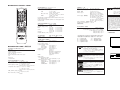
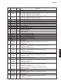
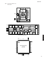
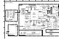
1
DVD AUDIO/VIDEO SA-CD PLAYER
DVD-S1700
SERVICE MANUAL
IMPORTANT NOTICE
This manual has been provided for the use of authorized YAMAHA Retailers and their service personnel.
It has been assumed that basic service procedures inherent to the industry, and more specifically YAMAHA Products, are already
known and understood by the users, and have therefore not been restated.
WARNING:
Failure to follow appropriate service and safety procedures when servicing this product may result in personal
injury, destruction of expensive components, and failure of the product to perform as specified. For these reasons,
we advise all YAMAHA product owners that any service required should be performed by an authorized
YAMAHA Retailer or the appointed service representative.
IMPORTANT: The presentation or sale of this manual to any individual or firm does not constitute authorization, certification or
recognition of any applicable technical capabilities, or establish a principle-agent relationship of any form.
The data provided is believed to be accurate and applicable to the unit(s) indicated on the cover. The research, engineering, and
service departments of YAMAHA are continually striving to improve YAMAHA products. Modifications are, therefore, inevitable
and specifications are subject to change without notice or obligation to retrofit. Should any discrepancy appear to exist, please
contact the distributor's Service Division.
WARNING:
Static discharges can destroy expensive components. Discharge any static electricity your body may have
accumulated by grounding yourself to the ground buss in the unit (heavy gauge black wires connect to this buss).
IMPORTANT: Turn the unit OFF during disassembly and part replacement. Recheck all work before you apply power to the unit.
DVD-S1700
■ CONTENTS
TO SERVICE PERSONNEL ...................................... 2–4
PREVENTION OF ELECTROSTATIC DISCHARGE .... 4
LOCALE MANAGEMENT INFORMATION ................... 4
FRONT PANEL .............................................................. 5
REAR PANELS .......................................................... 5–6
REMOTE CONTROL PANEL ........................................ 7
SPECIFICATIONS / 参考仕様 ........................................ 7
INTERNAL VIEW ........................................................... 8
TRADE MODE / トレードモード ................................... 8
ERROR MESSAGE / エラーメッセージ ........................ 8
101037
TROUBLESHOOTING / トラブルシュート ................... 8
DISASSEMBLY PROCEDURES / 分解手順 .................. 9
DISPLAY DATA ........................................................... 10
IC DATA ................................................................. 12–30
BLOCK DIAGRAM ....................................................... 31
WIRING DIAGRAM ...................................................... 32
PRINTED CIRCUIT BOARDS................................ 33–36
SCHEMATIC DIAGRAMS ...................................... 37–42
REPLACEMENT PARTS LIST .............................. 43–45
REMOTE CONTROL .................................................... 46
2006
All rights reserved.
This manual is copyrighted by YAMAHA and may not be copied or
redistributed either in print or electronically without permission.
P.O.Box 1, Hamamatsu, Japan
'06.12
DVD-S1700
■ TO SERVICE PERSONNEL
1. Critical Components Information
Components having special characteristics are
marked s and must be replaced with parts having
specifications equal to those originally installed.
WALL
OUTLET
2. Leakage Current Measurement (For 120V Models
Only)
When service has been completed, it is imperative to
verify that all exposed conductive surfaces are properly insulated from supply circuits.
●
Meter impedance should be equivalent to 1500 ohms
shunted by 0.15µF.
EQUIPMENT
UNDER TEST
AC LEAKAGE
TESTER OR
EQUIVALENT
INSULATING
TABLE
●
●
Leakage current must not exceed 0.5mA.
Be sure to test for leakage with the AC plug in both
polarities.
WARNING: CHEMICAL CONTENT NOTICE!
The solder used in the production of this product contains LEAD. In addition, other electrical/electronic and/or plastic (where
applicable) components may also contain traces of chemicals found by the California Health and Welfare Agency (and
possibly other entities) to cause cancer and/or birth defects or other reproductive harm.
DO NOT PLACE SOLDER, ELECTRICAL/ELECTRONIC OR PLASTIC COMPONENTS IN YOUR MOUTH FOR ANY REASON WHATSOEVER!
Avoid prolonged, unprotected contact between solder and your skin! When soldering, do not inhale solder fumes or expose
eyes to solder/flux vapor!
If you come in contact with solder or components located inside the enclosure of this product, wash your hands before
handling food.
DVD-S1700
About lead free solder / 無鉛ハンダについて
All of the P.C.B.s installed in this unit and solder joints are
soldered using the lead free solder.
本機に搭載されているすべての基板およびハンダ付けによる接合
部は無鉛ハンダでハンダ付けされています。
Among some types of lead free solder currently available,
it is recommended to use one of the following types for the
repair work.
無鉛ハンダにはいくつかの種類がありますが、修理時には下記の
ような無鉛ハンダの使用を推奨します。
• Sn + Ag + Cu (tin + silver + copper)
• Sn + Cu (tin + copper)
• Sn + Zn + Bi (tin + zinc + bismuth)
Caution:
As the melting point temperature of the lead free solder
is about 30°C to 40°C (50°F to 70°F) higher than that of
the lead solder, be sure to use a soldering iron suitable
to each solder.
・Sn+Ag+Cu
(錫+銀+銅)
・Sn+Cu
(錫+銅)
・Sn+Zn+Bi(錫+亜鉛+ビスマス)
注意:
無鉛ハンダの融点温度は通常の鉛入りハンダに比べ30∼40℃
程度高くなっていますので、それぞれのハンダに合ったハンダ
ごてをご使用ください。
WARNING: Laser Safety
This product contains a laser beam component. This component may emit invisible, as well as visible radiation,
which may cause eye damage. To protect your eyes and skin from laser radiation, the following precautions must be
used during servicing of the unit.
1) When testing and/or repairing any component within the product, keep your eyes and skin more than 30 cm away from
the laser pick-up unit at all times. Do not stare at the laser beam at any time.
2) Do not attempt to readjust, disassemble or repair the laser pick-up, unless noted elsewhere in this manual.
3) CAUTION : Use of controls, adjustments or performance of procedures other than those specified herein may result in
hazardous radiation exposure.
2
DVD-S1700
Laser Emitting conditions:
1) When the Top Cover is removed, and the STANDBY/ON SW is turned to the "ON" position, the laser component will emit
a beam for several seconds to detect if a disc is present. During this time (5-10 sec.) the laser may radiate through the
lens of the laser pick-up unit. Do not attempt any servicing during this period!
If no disc is detected, the laser will stop emitting the beam. When a disc is loaded, you will not be exposed to any laser
emissions.
2) The laser power level can be adjusted with the VR on the pick-up PWB, however, this level has been set by the factory
prior to shipping from the factory. Do not adjust this laser level control unless instruction is provided elsewhere in this
manual. Adjustment of this control can increase the laser emission level from the device.
Laser Diode Properties
Type:
Wave length:
Output Power:
Beam divergence:
Semiconductor laser GaAlAs
650 nm (DVD)
790 nm (VCD/CD)
1.45 mW (DVD)
1.13 mW (VCD/CD)
60 degrees
VARO!
: AVATTAESSA JA SUOJALUKITUS
OHITETTAESSA OLET ALTTIINA
NÄKYMÄTTÖMÄLLE LASERSÄTEILYLLE. ÄLÄ KATSO
SÄTEESEEN.
VARNING! : OSYNLIG LASERSTRÅLNING NÄR
DENNA DEL ÄR ÖPPNAD OCH
SPÄRREN ÄR URKOPPLAD.
BETRAKTA EJ STRÅLEN.
DVD-S1700
3
DVD-S1700
Warning for power supply
The primary side of the power supply carries live mains voltage when the player is connected to the mains even when
the player is switched off !
This primary area is not shielded so it is possible to touch copper tracks and/or components when servicing the player.
Service personnel have to take precautions to prevent touching this area or components in this area.
Note:
The screws on the DVD mechanism may never be touched, removed or re-adjusted.
Handle the DVD mechanism with care when the unit has to be exchanged!
The DVD mechanism is very sensitive for dropping or giving shocks.
■ PREVENTION OF ELECTROSTATIC DISCHARGE
The laser diode in the DVD mechanism may be damaged due to static electricity from clothes or the human body. Use caution
to prevent electrostatic damage when servicing or handling the DVD-mechanism.
1. Grounding for electrostatic damage prevention
Some devices, such as the DVD player, use an optical pickup (laser diode) that will be damaged by static electricity in the
working environment. Only attempt service after ensuring that all grounding procedures have been completed.
1. Worktable grounding
Put a grounded conductive material (sheet) or iron sheet on the area where the optical pickup is placed.
2. Human body grounding
Use an anti-static wrist strap to discharge the static electricity from your body.
Anti-static wrist strap
1M-ohms
Conductive material
(sheet) or steel sheet
2. Handling Precautions for DVD mechanism
1. Handle the DVD mechanism gently, as it is an extremely high-precision assembly.
DVD-S1700
2. The flexible cable lines may break if an excessive force is applied to it. Use caution when handling the cable.
3. The semi-fixed resistor for laser power adjustment should not be adjusted. Do not turn the resistor.
■ LOCALE MANAGEMENT INFORMATION
Locale Management Information : This DVD player is designed and manufactured to respond to the Locale
Management Information that is recorded on a DVD disc. If the Locale number described on the DVD disc does not
correspond to the Locale number of this DVD player, this DVD player cannot play this disc.
This product incorporates copyright protection technology that is protected by
method claims of certain U.S. patents and
other intellectual property rights owned by
Macrovision Corporation and other rights
owners. Use of this copyright protection
technology must be authorized by
Macrovision Corporation, and is intended
for home and other limited viewing uses
only unless otherwise authorized by
Macrovision Corporation. Reverse engineering or disassembly is prohibited.
5
2
1
6
3
5
4
2
4
2
5
4
DVD-S1700
■ FRONT PANEL
U, T, K, A, G, L, J models
■ REAR PANELS
U model
T model
DVD-S1700
K model
5
DVD-S1700
A model
G model
L model
DVD-S1700
J model
6
DVD-S1700
■ REMOTE CONTROL PANEL
VIDEO PERFORMANCE / ビデオ部
Video (CVBS) output
1 Vpp into 75 ohms
S-video output
Y: 1 Vpp into 75 ohms
C: 0.3 Vpp into 75 ohms
D1/D2 output (J model) Y: 1 Vpp into 75 ohms
PB/CB, PR/CR: 0.7 Vpp into 75 ohms
Component video output (U, T, K, A, G, L models)
Y: 1 Vpp into 75 ohms
PB/CB, PR/CR: 0.7 Vpp into 75 ohms
RGB (SCART) output (G model)
0.7 Vpp into 75 ohms
Black level shift (U model)
On/Off
U ........ U.S.A. model
K ........ Korean model
G ........ European model
J ......... Japanese model
7
T ........ Chinese model
A ........ Australian model
L ........ Singapore model
Manufactured under license from Dolby Laboratories. “Dolby” and the double-D symbol are
trademarks of Dolby Laboratories.
ドルビーラボラトリーズからの実施権により製造され
ています。「ドルビー」およびダブルD 記号は、ドル
ビーラボラトリーズの商標です。
“DTS” and “DTS Digital Surround” are registered trademarks of Digital Theater Systems,
Inc.
DTSおよびDTS Digital Surroundはデジタルシア
ターシステムズの登録商標です。
DivX, DivX Certified, and associated logos are
trademarks of DivX, Inc. and are used under
license.
435 (17-1/8")
(1/4")
* Specifications are subject to change without prior notice.
※ 参考仕様および外観は予告なく変更されることがあります。
284.5 (11-3/16")
CONNECTIONS / 接続端子
Video output
Cinch (yellow) x 1
S-video output
Mini DIN, 4 pins x 1
D1/D2 output (J model) 1
Component video output
Y output
Cinch (green) x 1
PB/CB output
Cinch (blue) x 1
Cinch (red) x 1
PR/CR output
SCART (G model)
Euroconnector x 1
Digital output
Coaxial x 1
Optical x 1
IEC60958 for CDDA/LPCM,
IEC61937 for MPEG 1/2,
Dolby Digital and DTS
HDMI
Type A x 1
Audio output
2 channel analog output
MIXED 2CH L/R Cinch (white/red) x 1 pair
Multi channel analog output
FRONT L/R
Cinch (white/red) x 1 pair
SURROUND L/R Cinch (white/red) x 1 pair
CENTER
Cinch (black) x 1
SUBWOOFER
Cinch (black) x 1
• DIMENSIONS
273.5 (10-3/4")
(PAL: 50 Hz) (NTSC: 60 Hz)
625
525
Multistandard (PAL/NTSC)
Remote control x 1
Battery (AAA, R03, UM-4) x 2
Power cable (2 m) x 1 (U, T, A, G, L, J models)
Power cable (2 m) x 2 (K model)
Video pin cable (1 m) x 1
Audio pin cable (1 m) x 1
本製品は、著作権保護技術を採用しており、マクロビジョン社及びその
他の著作権利者が保有する米国特許及びその他の知的財産権によって保
護されています。この著作権保護技術の使用は、マクロビジョン社の許
可が必要で、またマクロビジョン社の特別な許可がない限り家庭用及び
その他の一部の視聴用の使用に制限されています。分解したり、改造す
ることも禁じられています。
87 (3-7/16")
PLAYBACK SYSTEM / 対応ディスク
DVD-video
DVD-audio
DVD-R, DVD-RW
DVD+R, DVD+RW, DVD+R DL
Video CD, SVCD
SA-CD multi-channel and SA-CD stereo
CD
Picture CD
CD-R, CD-RW
kHz
kHz
kHz
kHz
kHz
This product incorporates copyright protection technology that
is protected by method claims of certain U.S. patents and
other intellectual property rights owned by Macrovision Corporation and other rights owners. Use of this copyright protection
technology must be authorized by Macrovision Corporation,
and is intended for home and other limited viewing uses only
unless otherwise authorized by Macrovision Corporation. Reverse engineering or disassembly is prohibited.
4
■ SPECIFICATIONS / 参考仕様
44
22
22
20
20
H D M I 、H D M I ロゴおよびH i g h - D e f i n i t i o n
Multimedia Interfaceは、HDMI Licensing LLCの
商標または、登録商標です。
(3/16")
TV STANDARD
Number of lines
Playback
ACCESSORIES / 付属品
to
to
to
to
to
“HDMI”, the “HDMI” logo and “High Definition
Multimedia Interface” are trademarks or registered trademark of HDMI Licensing LLC.
70 (2-3/4")
/ オーディオ特性
24 bits, 192 kHz
115 dB
105 dB
fs 96 kHz
2 Hz
fs 48 kHz
2 Hz
SVCD
fs 48 kHz
2 Hz
fs 44.1 kHz
2 Hz
CD/VCD
fs 44.1 kHz
2 Hz
Distortion and noise (1 kHz) 0.002 %
AUDIO PERFORMANCE
DA converter
Signal to noise (1 kHz)
Dynamic range (1 kHz)
DVD
435 x 87 x 284.5 mm
(17-1/8" x 3-7/16" x 11-3/16")
3.3 Kg (7 lbs. 4 oz)
Gold color (K, J models)
Black color (U, A, G models)
Titanium color (T, G, L models)
Power supply / 電源電圧
AC 120 V, 60 Hz (U model)
AC 100-240 V, 50 Hz (T model)
AC 100-240 V, 50/60 Hz
(K, A, L models)
AC 230 V, 50 Hz (G model)
AC 100 V, 50/60 Hz (J model)
Power consumption / 消費電力 Approx. 21 W
Standby power consumption / < 0.5 W
待機時消費電力
17
Full decoding of Dolby Digital and DTS multi-channel sound
Analog stereo sound
Dolby surround compatible downmix from Dolby Digital multichannel sound
GENERAL / 一般
Dimensions (W x H x D) /
寸法
(幅 x 高さ x 奥行き)
Weight / 質量
Finish / 仕上げ
(11/16")
AUDIO FORMAT / オーディオフォーマット
Digital Dolby Digital/DTS/MPEG
Compressed Digital
PCM
16, 20, 24 bits
fs 44.1, 48, 88.2, 96 kHz
MP3 (ISO 9660) 32 kbps to 320 kbps
fs 16, 22.05, 24, 32, 44.1, 48 kHz
WMA
64 kbps to 320 kbps
mono, stereo
Unit: mm (inch)
単位:mm
(インチ)
DivX、DivX Certified、および関連するロゴは、
DivX, Inc.の商標です。これらの商標は、DivX, Inc.
の使用許諾を得て使用しています。
“DCDi” is a trademark of Faroudja, a division of
Genesis Microchip, Inc.
DCDiは、Genesis Microchip Inc.の事業部門である
Faroudjaの商標です。
7
DVD-S1700
■ INTERNAL VIEW
1
■ ERROR MESSAGE / エラーメッセージ
2
3
4
Display / 表示
1
2
3
4
5
6
POWER SUPPLY UNIT
DVD MECHANISM UNIT
MAIN (1) P.C.B.
MAIN (4) P.C.B. (G model)
MAIN (2) P.C.B.
MAIN (3) P.C.B.
Cause / 原因
NO DISC
When no disc is loaded in the tray. / ディスクがトレイにセットされていない場合。
UNKNOWN DISC
When a disc which cannot be played or recognized is loaded in the tray. /
再生できない、または認識できないディスクがトレイにセットされている場合。
■ TROUBLESHOOTING / トラブルシュート
・ HDMIリセット
• HDMI Reset
6
When no picture is displayed even though the main unit
and TV monitor are connected with the HDMI cable
1. Press the “STOP” key of the main unit or on the remote control twice.
2. While pressing the “STOP” key of the main unit, press
the “PLAY/PAUSE” key for 3 seconds or longer.
3. [HDMI RESE] is displayed of the main unit which then
returns to the normal display.
5
■ TRADE MODE / トレードモード
In the TRADE mode, the tray open/close function is stopped
temporarily.
トレードモードは、トレイのOPEN/CLOSE機能を一時的に停止
する機能です。
• Setting TRADE mode
・ トレードモードの起動
1. Connect the power cable of the main unit to the AC
outlet.
2. Press the “STANDBY/ON” key of the main unit or remote controller to turn on the power.
3. Press the “OPEN/CLOSE” key of the main unit to open
the tray.
4. Place a disc in the tray and open the “OPEN/CLOSE”
key of the main unit to close the tray.
5. While pressing the “SKIP+/SEARCH+” key of the
main unit and press the “STOP” key for 3 seconds
or longer.
6. When the TRADE mode is set, [TRADE ON] is displayed which then returns to the normal display.
Note: Even after the TRADE mode is set, all functions remain the same as normal except the
“OPEN/ CLOSE” key.
Press the “OPEN/CLOSE” key, and [TRAY
LOCKED] is displayed.
• Canceling TRADE mode
1. With a disc set in the tray, while pressing the “SKIP+/
SEARCH+” key of the main unit and press the “STOP”
key for 3 seconds or longer.
2. When the TRADE mode is cancelled, [TRADE OFF]
is displayed which then returns to the normal display.
8
1. 本機の電源コードをACコンセントに接続します。
2. 本機またはリモコンの
“STANDBY/ON”
キーを押し、電源
を入れます。
3. 本機の
“OPEN/CLOSE”
キーを押し、トレイを開きます。
4. トレイにディスクをセットし、本機の“OPEN/CLOSE”
キーを押しトレイを閉じます。
本機とTVモニターをHDMIケーブルで接続しても映像が表示
されない場合
1. 本機の“STOP”キーまたは、リモコンの“STOP”キーを2
回押します。
2. 本機の
“STOP”
キーを押しながら
“PLAY/PAUSE”
キーを
3秒間以上押し続けます。
3. 本機のディスプレイに「HDMI RESET」と表示した後、通
常の表示に戻ります。
・ ビデオリセット
• VIDEO Reset
When no picture is displayed or picture is displayed but
not properly even though the main unit and TV monitor
are connected with the video pin cable or the like
1. Press the “EJECT” key to open the tray.
2. Press the “CLEAR” key on the remote control.
3. Press the “2”, “5”, “8” and “0” keys on the remote control.
4. Press the “AUDIO” key on the remote control.
本機とTVモニターを映像ピンケーブルなどで接続しても映像
が表示されない、または映像が正しく表示されない場合
1. 本機の“EJECT”キーを押してトレイを開きます。
2. リモコンの“CLEAR”キーを押します。
3. リモコンの“2”、“5”、“8”、“0”キーを押します。
4. リモコンの“AUDIO”キーを押します。
Remote control / リモコン
5. 本機の“S K I P + / S E A R C H + ”キーを押しながら次に
“STOP”キーを3秒間以上押し続けます。
6. トレードモードが起動し
「TRADE ON」
と表示した後、通常
の表示に戻ります。
注:
トレードモード起動後、“OPEN/CLOSE”キー以
外の操作は通常通り行うことができます。
“OPEN/CLOSE”
キーを押すと
「TRAY LOCKED」
と表示されます。
Main unit / 本機
Tray
"EJECT" key
・ トレードモードの解除
1. トレイにディスクがセットされている状態で、本機の
“SKIP+/SEARCH+”キーを押しながら次に“STOP”キー
を3秒間以上押し続けます。
2. トレードモードが解除され
「TRADE OFF」
と表示した後、
通常の表示に戻ります。
"PLAY/PAUSE" key
"STOP" key
DVD-S1700
e. Remove CN11, CN12 and CN13. (Fig. 2)
f. Lift up the rear side of the DVD mechanism unit, then
■ DISASSEMBLY PROCEDURES / 分解手順
(Remove parts in disassembly order as numbered.)
f. DVDメカユニットの後ろを持ち上げ、フック2箇所を外し、
remove 2 hooks and remove rearward. (Fig. 1)
(番号順に部品を取り外してください。)
Disconnect the power cable from the AC outlet.
e. CN11、CN12、CN13を外します。(Fig. 2)
後方へ取り外します。(Fig. 1)
AC電源コンセントから、電源コードを抜いてください。
DVD mechanism unit
DVDメカユニット
Solder
1. Removal of Top Cabinet
1. トップカバーの外し方
a. Remove 6 screws (1). (Fig. 1)
b. Lift up the rear side of the top cover, then remove rear-
a. 1のネジ6本を外します。(Fig. 1)
MAIN (1) P.C.B.
b. トップカバーの後ろを持ち上げ、後方へ取り外します。
(Fig. 1)
ward. (Fig. 1)
CN11
DVD mechanism unit
DVDメカユニット
2
1
CN13
1
1
Tray lid
トレイリッド
CX41
3
CN12
Fig. 2
Hook
フック
Top cover
トップカバー
5
1
4
Hook
フック
5
Front panel ass'y
フロントパネルASS'Y
Front panel ass'y
Hook
フロントパネルASS'Y フック
3. Removal of Front Panel Ass’y
3. フロントパネルASS’Yの外し方
a. Remove 3 screws (3) and 4 screws (4). (Fig. 1)
b. Remove 2 screws (5). (Fig. 1)
a. 3のネジ3本、4のネジ4本を外します。(Fig. 1)
c. Remove CX41. (Fig. 2)
d. Remove 2 hooks and then remove the front panel ass’y
c. CX41を外します。(Fig. 2)
forward. (Fig. 1)
b. 5のネジ2本を外します。(Fig. 1)
d. フック2箇所を外し、フロントパネルASS’Yを前方へ取り外
します。(Fig. 1)
Hook
フック
Front
Front panel ass'y
フロントパネルASS'Y
Front
DVD mechanism unit
DVDメカユニット
• How to manually eject the tray / 手動でトレイを開く方法
a. Turn the unit bottom up.
b. Turn the loading gear in the direction indicated with a
flatblade screwdriver until the tray is ejected.
c. Gently pull the tray out.
a. 本機を上下反転します。
b. トレイが出てくるまで、マイナスドライバーでローディングギ
アを図に示す矢印の方向に回転します。
c. トレイをそっと引き出します。
Fig. 1
Flatblade screwdriver
マイナスドライバー
2. Removal of DVD Mechanism Unit
2. DVDメカユニットの外し方
a. Eject the tray. (See “How to manually eject the tray”.)
b. Remove the tray lid and close the tray. (Fig. 1)
b. トレイリッドを外し、トレイを閉じます。(Fig. 1)
c. Remove 2 screws (2). (Fig. 1)
d. Solder the lands in the P.C.B. of the DVD mechanism
unit with the anti-static soldering iron. (Fig. 2)
Note
• After you have finished repairing , connect the
flexible flat cable to CN11 in advance and then remove the solder from the short-circuit location
Loading gear
ローディングギア
a. トレイを開きます。(“手動でトレイを開く方法”を参照)
c. 2のネジ2本を外します。(Fig. 1)
d. DVDメカユニットの基板上の端子間を静電気対策はんだこて
を使用してショートします。(Fig. 2)
注意
Tray
トレイ
Tray
トレイ
・ 修理終了時は、先にカード電線をCN11に接続し、次に静電
気対策はんだこてを使用してショート箇所からはんだを除去
します。
with the anti-static soldering iron.
9
DVD-S1700
■ DISPLAY DATA
● ANODE CONNECTION
● F401 : HCA14SM16 (AAX80850)
j
1
PATTERN AREA
● PIN CONNECTION
Pin No.
50 49 48 47 46 45 44 43 42 41 40 39 38 37 36 35 34 33 32 31 30 29 28 27 26
Connection F2 F2 NP NP NX NX NX NX NX NX NX NX NX NX NX NX NX NX NX NX NX NX NX NX NX
Pin No.
25 24 23 22 21 20 19 18 17 16 15 14
13
12
11
10
9
8
7
6
5
4
3
2
1
Connection NX NX NX NX NX NX NX NX NX 1G NC GR1 VDD DIN CLKB CSB RSTB OSCO OSCI VEE GND NP NP F1 F1
Note : 1) F1, F2 ..... Filament pin
2) NP ..... No pin
3) NC ..... No connection
4) NX ..... No extended pin
● GRID ASSIGNMENT
1G
14G
13G
12G
11G
10G
9G
8G
7G
1
2
3
4
5
6
7
8
9
10
11
12
13
14
15
16
17
18
19
20
21
22
23
24
25
26
27
28
29
30
31
32
33
34
35
(2G-14G)
10
6G
5G
4G
3G
2G
SG1
SG2
SG3
SG4
SG5
SG6
SG7
SG8
SG9
SG10
SG11
SG12
SG13
SG14
SG15
SG16
SG17
SG18
SG19
SG20
SG21
SG22
SG23
SG24
SG25
SG26
SG27
SG28
SG29
SG30
SG31
SG32
SG33
SG34
SG35
GR14 GR13 GR12 GR11 GR10
14G
13G
12G
11G
10G
1
1
1
1
1
2
2
2
2
2
3
3
3
3
3
4
4
4
4
4
5
5
5
5
5
6
6
6
6
6
7
7
7
7
7
8
8
8
8
8
9
9
9
9
9
10
10
10
10
10
11
11
11
11
11
12
12
12
12
12
13
13
13
13
13
14
14
14
14
14
15
15
15
15
15
16
16
16
16
16
17
17
17
17
17
18
18
18
18
18
19
19
19
19
19
20
20
20
20
20
21
21
21
21
21
22
22
22
22
22
23
23
23
23
23
24
24
24
24
24
25
25
25
25
25
26
26
26
26
26
27
27
27
27
27
28
28
28
28
28
29
29
29
29
29
30
30
30
30
30
31
31
31
31
31
32
32
32
32
32
33
33
33
33
33
34
34
34
34
34
35
35
35
35
35
GR9
9G
1
2
3
4
5
6
7
8
9
10
11
12
13
14
15
16
17
18
19
20
21
22
23
24
25
26
27
28
29
30
31
32
33
34
35
GR8
8G
1
2
3
4
5
6
7
8
9
10
11
12
13
14
15
16
17
18
19
20
21
22
23
24
25
26
27
28
29
30
31
32
33
34
35
GR7
7G
1
2
3
4
5
6
7
8
9
10
11
12
13
14
15
16
17
18
19
20
21
22
23
24
25
26
27
28
29
30
31
32
33
34
35
GR6
6G
1
2
3
4
5
6
7
8
9
10
11
12
13
14
15
16
17
18
19
20
21
22
23
24
25
26
27
28
29
30
31
32
33
34
35
GR5
5G
1
2
3
4
5
6
7
8
9
10
11
12
13
14
15
16
17
18
19
20
21
22
23
24
25
26
27
28
29
30
31
32
33
34
35
GR4
4G
1
2
3
4
5
6
7
8
9
10
11
12
13
14
15
16
17
18
19
20
21
22
23
24
25
26
27
28
29
30
31
32
33
34
35
GR3
3G
1
2
3
4
5
6
7
8
9
10
11
12
13
14
15
16
17
18
19
20
21
22
23
24
25
26
27
28
29
30
31
32
33
34
35
GR2
2G
1
2
3
4
5
6
7
8
9
10
11
12
13
14
15
16
17
18
19
20
21
22
23
24
25
26
27
28
29
30
31
32
33
34
35
GR1
1G
DVD-S1700
MEMO
DVD-S1700
MEMO
11
DVD-S1700
■ IC DATA
IC11: ZR36778 (MAIN P.C.B.)
MPEG decoder
IR-RC
Receiver
Front Panel
Concentrator
SPI/I2C/GPIO/DDC
8/16 Mbits
NOR
Flash
v
TRAY
v
MICROPROCESSOR
SPINDLE
SERVO
v
RESET
Vaddis
778
v
v
AFE
Disc loader
VPU
ADP
DSP
ADC
S/PDIF
DVD-S1700
Stereo
Mics
DAC
2 to 8
Speakers
TV
Monitor
v
Audio
12
32/64/128
Mbits
SDRAM
MCU
v
OPU
RF amp
v
SLED
27 MHz
PLL
Servo amp
DVD-S1700
No.
1
2
3
4,5
6
7
8
9
10
11
12
13
14
15
16
17
18-19
20
23
24
25
26
27
28
29
30
31
32
33
34
35
36
37
38
SSCRXD
GPCI/O[17]
PM[15]
MEMCS[1]#
GPCI/O[18]
VDDP
MEMAD
[15,16]
SYSIND[1,0]
MEMAD[14]
GCLKSEL
MEMAD[13]
FCUIF[29]
MEMAD[12]
PLLCFGA
MEMDA[15]
FCUIF[28]
MEMAD[11]
PLLCFGP
MEMDA[7]
FCUIF[9]
GNDP
MEMAD[10]
FCUIF[20]
MEMDA[14]
FCUIF[27]
MEMAD[9]
FCUIF[19]
MEMDA[6]
FCUIF[8]
MEMAD[8]
FCUIF[18]
MEMDA[13,5]
FCUIF[26,7]
MEMAD[20]
MEMCS[2]#
GPCI/O[19]
VDDP
MEMDA[12]
FCUIF[25]
MEMWR#
FCUIF[0]
MEMDA[4]
FCUIF[6]
VDDC
MEMDA[11]
FCUIF[24]
MEMDA[3]
FCUIF[5]
MEMAD[19]
PLLSEL
GNDC
MEMDA[10]
FCUIF[23]
MEMAD[18]
GNDP
MEMDA[2]
FCUIF[4]
MEMAD[17]
MEMDA[9]
FCUIF[22]
MEMAD[7]
FCUIF[17]
MEMDA[1]
FCUIF[3]
MEMAD[6]
Description
I
I/O
O
O
I/O
S
O
SSC data input
General purpose I/O, monitored/controlled by the microprocessor or DSP or FCU SW
Probe mux data output
PNVM/SRAM chip select (active low) output
General purpose I/O, monitored/controlled by the microprocessor or DSP SW
3.3 V digital periphery power supply
PNVM/SRAM address bus outputs
I
O
I
O
O
O
I
I/O
I/O
O
I
I/O
I/O
S
O
O
I/O
I/O
O
O
I/O
I/O
O
O
I/O
I/O
O
O
I/O
S
I/O
I/O
O
O
I/O
O
S
I/O
I/O
I/O
I/O
O
I
S
I/O
I/O
O
S
I/O
I/O
O
I/O
I/O
O
O
I/O
I/O
O
General purpose system configuration indication input / Level sampled during RESET
PNVM/SRAM address bus output
GCLKPOUT or GCLKA function selection / Level sampled during RESET
PNVM/SRAM address bus output
Flash card interface unit output signal
PNVM/SRAM address bus output
Audio PLL configuration input / Level sampled during RESET / In normal operation the pin must be low during RESET
PNVM/SRAM bi-directional data bus
Flash card interface unit I/O signal
PNVM/SRAM address bus output
Process PLL configuration input / Level sampled during RESET / In normal operation the pin must be low during RESET
PNVM/SRAM bi-directional data bus
Flash card interface unit I/O signals
Digital periphery ground of 3.3 V supply
PNVM/SRAM address bus output
Flash card interface unit output signal
PNVM/SRAM bi-directional data bus
Flash card interface unit I/O signal
PNVM/SRAM address bus outputs
Flash card interface unit output signal
PNVM/SRAM bi-directional data bus
Flash card interface unit I/O signals
PNVM/SRAM address bus outputs
Flash card interface unit output signal
PNVM/SRAM bi-directional data bus
Flash card interface unit I/O signals
PNVM/SRAM address bus outputs
PNVM/SRAM chip select (active low) output
General purpose I/O, monitored/controlled by the microprocessor or DSP SW
3.3 V digital periphery power supply
PNVM/SRAM bi-directional data bus
Flash card interface unit I/O signal
PNVM/SRAM write enable (active low) output
Flash card interface unit output signal
PNVM/SRAM bi-directional data bus
Flash card interface unit output signal
1.8 V digital core power supply
PNVM/SRAM bi-directional data bus
Flash card interface unit I/O signal
PNVM/SRAM bi-directional data bus
Flash card interface unit I/O signals
PNVM/SRAM address bus outputs
PLL frequency selection -108 MHz (low) or 135 MHz (high) / Level sampled during RESET
Digital core ground of 1.8 V supply
PNVM/SRAM bi-directional data bus
Flash card interface unit I/O signal
PNVM/SRAM address bus output
Digital periphery ground of 3.3 V supply
PNVM/SRAM bi-directional data bus
Flash card interface unit I/O signals
PNVM/SRAM address bus output
PNVM/SRAM bi-directional data bus
Flash card interface unit I/O signal
PNVM/SRAM address bus outputs
Flash card interface unit output signal
PNVM/SRAM bi-directional data bus
Flash card interface unit I/O signals
PNVM/SRAM address bus outputs
DVD-S1700
21
22
Pin Functions Direction
13
DVD-S1700
No.
O
I/O
I/O
O
O
S
I/O
O
I/O
O
O
I/O
O
O
O
O
O
I
49
MEMAD[0]
FCUIF[10]
BOOTSEL[1]
O
O
I
50
51
52
53-57
GNDP
VDD-IP
VDDP
RAMADD
[4, 3, 5, 2, 6]
VDDP
RAMADD
[1, 7, 0]
GNDP
RAMADD[8]
VDDC
RAMADD[10]
GNDC
RAMADD[9]
VDDP
RAMADD[11]
RAMCS[0]#
RAMBA[1]
RAMBA[0]
GNDP
RAMCS[1]#
RAMRAS#
RAMCAS#
VDDP
RAMWE#
RAMDQM
GNDPCLK
PCLK
VDDPCLK
RAMDAT[8]
GNDP
RAMDAT
[7, 9, 6]
VDDP
RAMDAT
[10, 5, 11]
GNDP
S
S
S
O
Flash card interface unit output signal
PNVM/SRAM bi-directional data bus
Flash card interface unit I/O signal
PNVM/SRAM address bus outputs
Flash card interface unit output signal
3.3 V digital periphery power supply
PNVM/SRAM bi-directional data bus
Flash card interface unit output signal
PNVM/SRAM address bus outputs
Flash card interface unit output signal
PNVM/SRAM read enable (active low) output
Flash card interface unit I/O signal
PNVM/SRAM address bus outputs
Flash card interface unit output signal
PNVM/SRAM chip select (active low) output
PNVM/SRAM address bus outputs
Flash card interface unit output signals
Microprocessor SW boot (and execute) source selection:
(high, high) - For production testing;
(high, low) - Flash+SRAM (for debug monitor);
(low, high) - First debug UART
(low, low) - Flash (low) or Level sampled during RESET
PNVM/SRAM address bus outputs
Flash card interface unit output signals
Microprocessor SW boot (and execute) source selection:
(high, high) - For production testing;
(high, low) - Flash+SRAM (for debug monitor);
(low, high) - First debug UART
(low, low) - Flash (low) or Level sampled during RESET
Digital periphery ground of 3.3 V supply
3.3 V periphery reference voltage
3.3 V digital periphery power supply
SDRAM address bus output
S
O
3.3 V digital periphery power supply
SDRAM address bus output
S
O
S
O
S
O
S
O
O
O
O
S
O
O
O
S
O
O
S
O
S
I/O
S
I/O
Digital periphery ground of 3.3 V supply
SDRAM address bus output
1.8 V digital core power supply
SDRAM address bus output
Digital core ground of 1.8 V supply
SDRAM address bus output
3.3 V digital periphery power supply
SDRAM address bus output
SDRAM chip select (active low)
SDRAM bank select output
SDRAM bank select output
Digital periphery ground of 3.3 V supply
SDRAM chip select (active low) output
SDRAM row select (active low) output
SDRAM column select (active low) output
3.3 V digital periphery power supply
SDRAM write enable (active low) output
SDRAM data masking (active high) output
Digital ground of filtered 3.3 V supply for PCLK
SDRAM clock output (same as internal processing clock)
3.3 V filtered digital power supply for PCLK
SDRAM bi-directional data bus
Digital periphery ground of 3.3 V supply
SDRAM bi-directional data bus
S
I/O
3.3 V digital periphery power supply
SDRAM bi-directional data bus
40
41
42
43
44
45-46
47
48
58
59-61
62
63
64
65
66
67
68
69
70
DVD-S1700
Description
FCUIF[16]
MEMDA[8]
FCUIF[21]
MEMAD[5]
FCUIF[15]
VDDP
MEMDA[0]
FCUIF[2]
MEMAD[4]
FCUIF[14]
MEMRD#
FCUIF[1]
MEMAD[3, 2]
FCUIF[13, 12]
MEMCS[0]#
MEMAD[1]
FCUIF[11]
BOOTSEL[2]
39
71
72
73
74
75
76
77
78
79
80
81
82
83
84-86
87
88-90
91
14
Pin Functions Direction
S
Digital periphery ground of 3.3 V supply
DVD-S1700
No.
92
93
94
95
96
97
98-100
Pin Functions Direction
Description
SDRAM bi-directional data bus
1.8 V digital core power supply
SDRAM bi-directional data bus
Digital core ground of 1.8 V supply
SDRAM bi-directional data bus
3.3 V digital periphery power supply
SDRAM bi-directional data bus
S
I/O
Digital periphery ground of 3.3 V supply
SDRAM bi-directional data bus
S
I/O
I
I
O
S
I/O
109
AOUT[3]
SDATA[1]
PM[1]
IDGPCI/O[0]
O
I
O
I/O
RAMCKE
SDATA[2]
PM[2]
S/PDIFOUT
SDATA[3]
PM[3]
AOUT[2]
GPCI/O[21]
SDATA[4]
PM[4]
AOUT[1]
GPCI/O[22]
PM[5]
AOUT[0]
SDATA[6]
PM[6]
GPAI/O
AOUT[3]
IDGPCI/O[0]
O
I
O
O
I
O
O
I/O
I
O
O
I/O
O
O
I
O
I/O
O
I/O
PM[7]
ALRCLK
ABCLK
O
O
O
GNDP-A2
AMCLK
VDDP-A2
AIN
GPCI/O[23]
PM[8]
GNDC
VSYNC#
HDFI
GPI/O[24]
DACTEST[9]
PM[9]
VDDC
HSYNC#
HDHS
GPCI/O[25]
GNDP
VCLKx2
S
I/O
S
I
I/O
O
S
O
I
I/O
I
O
S
O
I
I/O
S
O
3.3 V digital periphery power supply
General purpose I/O, monitored/controlled by the microprocessor or DSP SW
Microprocessor non-maskable interrupt input
SERVO channel sample data input for AFE by-pass
Probe mux data output
Digital periphery ground of 3.3 V supply
General purpose I/O, monitored/controlled by the microprocessor or DSP SW
When input, the pin can be used as general purpose external interrupt to the microprocessor
Serial output of digital stereo audio
SERVO channel sample data input for AFE by-pass
Probe mux data output
General purpose I/O, monitored/controlled by the microprocessor or DSP SW
When input, the pin can be used as general purpose external interrupt to the DSP
Clock enable signal to the SDRAM (for power down)
SERVO channel sample data input for AFE by-pass
Probe mux data output
S/PDIF transmitter output for digital coded or reconstructed audio data
SERVO channel sample data input for AFE by-pass
Probe mux data output
Serial outputs of digital stereo audio
General purpose I/O, monitored/controlled by the microprocessor or DSP SW
SERVO channel sample data inputs for AFE by-pass
Probe mux data outputs
Serial output of digital stereo audio
General purpose I/O, monitored/controlled by the microprocessor or DSP SW
Probe mux data outputs
Serial output of digital stereo audio
SERVO channel sample data input for AFE by-pass
Probe mux data outputs
General purpose I/O, monitored/controlled by the ADP SW
Serial output of digital stereo audio
General purpose I/O, monitored/controlled by the microprocessor or DSP SW
When input, the pin can be used as general purpose external interrupt to the DSP
Probe mux data output
Digital audio left/right select output for the audio port / Square wave, at the sampling frequency / Programmable polarity
Digital audio bit-clock output / Data on AOUT and AIN is output or latched, respectively, with the rising or
falling (programmable) edge of this clock
Digital ground filtered 3.3 V supply for AMCLK
Audio master clock I/O / 128, 192, 256 or 384 times the sampling frequency (programmable)
3.3 V filtered digital power supply for AMCLK
Serial input of digital stereo audio
General purpose I/O, monitored/controlled by the microprocessor or DSP SW
Probe mux data output
Digital core ground of 1.8 V supply
SD digital video vertical sync output signal
HD digital video field index input signal
General purpose I/O, monitored/controlled by the microprocessor or DSP SW
DACs test input
Probe mux data output
1.8 V digital core power supply
SD digital video horizontal sync output signal
HD digital video horizontal sync input signal
General purpose I/O, monitored/controlled by the microprocessor or DSP SW
Digital periphery ground of 3.3 V supply
Digital video clock output / 27,000 (for SD interlaced), 54,000 (SD progressive) or 135,000 (for HD) MHz
101
102-104
105
106
110
111
112
113
114
115
116
117
118
119
120
121
122
123
124
125
126
DVD-S1700
I/O
S
I/O
S
I/O
S
I/O
107
108
RAMDAT[4]
VDDC
RAMDAT[12]
GNDC
RAMDAT[3]
VDDP
RAMDAT
[13, 2, 14]
GNDP
RAMDAT
[1, 15, 0]
VDDP
GPCI/O[20]
CPUNMI
SDATA[0]
PM[0]
GNDP
ICGPCI/O[0]
15
DVD-S1700
No.
COSYNC
ICGPCI/O[1]
O
I/O
VDDP
VID[7]
GPCI/O[26]
VID[6]
ICGPCI/O[2]
S
O
I/O
O
I/O
130
VID[5]
IDGPCI[1]
O
I/O
131
132
GNDP
VID[4]
GPCI/O[27]
VID[3]
GPCI/O[28]
SERVOCLK
VID[2]
GPCI/O[29]
SSEL[0]
VDDP
VID[1]
GPCI/O[30]
SSEL[1]
VID[0]
ICGPCI/O[3]
S
O
I/O
O
I/O
O
O
I/O
O
S
O
I/O
O
O
I/O
138
139
140
141
142
GNDP
GNDA
RESET#
VDDA
XO
S
S
ID
S
AO
143
144
GCLKP
GCLKA
GPCI/O[31]
GCLKPOUT
VDDP
ICGPCI/O[4]
ID
ID
I/O
O
S
I/O
S/PDIFIN[0]
GPCI/O[33]
ICGPCI/O[5]
I
I/O
I/O
S/PDIFIN[1]
GPCI/O[34]
IDGPCI/O[3]
I
I/O
I/O
FCUIF[33]
GNDP
DUPRD0
GPCI/O[35]
DUPTD0
GPCI/O[36]
VDD-IP
DUPRD1
GPCI/O[37]
DUPTD1
GPCI/O[38]
GNDDACD
CVBS/G/Y
(DAC A)
I
S
I
I/O
O
I/O
S
I
I/O
O
I/O
S
AO
CVBS/C
(DAC D)
AO
127
128
129
133
134
135
136
137
DVD-S1700
145
146
147
148
149
150
151
152
153
154
155
156
157
158
159
16
Pin Functions Direction
Description
Composite sync output / Active only when component analog output is selected
General purpose I/O, monitored/controlled by the microprocessor or DSP SW
When input, the pin can be used as general purpose external interrupt to the microprocessor
3.3 V digital periphery power supply
Digital 4: 2: 2 video luma/chroma output, interleaved U, Y V Y
General purpose I/O, monitored/controlled by the microprocessor or DSP SW
Digital 4: 2: 2 video luma/chroma output, interleaved U, Y V Y
General purpose I/O, monitored/controlled by the microprocessor or DSP SW
When input, the pin can be used as general purpose external interrupt to the microprocessor
Digital 4: 2: 2 video luma/chroma output, interleaved U, Y V Y
General purpose I/O, monitored/controlled by the microprocessor or DSP SW
When input, the pin can be used as general purpose external interrupt to the DSP
Digital periphery ground of 3.3 V supply
Digital 4: 2: 2 video luma/chroma output, interleaved U, Y V Y
General purpose I/O, monitored/controlled by the microprocessor or DSP SW
Digital 4: 2: 2 video luma/chroma output, interleaved U, Y V Y
General purpose I/O, monitored/controlled by the microprocessor or DSP SW
SERVO channel clock output for AFE by-pass
Digital 4: 2: 2 video luma/chroma output, interleaved U, Y V Y
General purpose I/O, monitored/controlled by the microprocessor or DSP SW
SERVO channel select output for AFE by-pass
3.3 V digital periphery power supply
Digital 4: 2: 2 video luma/chroma output, interleaved U, Y V Y
General purpose I/O, monitored/controlled by the microprocessor or DSP SW
SERVO channel output for AFE by-pass
Digital 4: 2: 2 video luma/chroma output, interleaved U, Y V Y
General purpose I/O, monitored/controlled by the microprocessor or DSP SW
When input, the pin can be used as general purpose external interrupt to the microprocessor
Digital periphery ground of 3.3 V supply
Ground plane of internal PLL circuit
Reset input (active low)
1.8 V power supply for internal PLL circuit
Output to a crystal that is connected to GCLKP
If a crystal is not used at GCLKP, XO must be left not connected.
27.000MHz clock or crystal input for main processing clock generation.
27.000MHz clock input for audio master clock generation.
General purpose I/O, monitored/controlled by the microprocessor or DSP SW
GCLKP output
3.3 V digital periphery power supply
General purpose I/O, monitored/controlled by the microprocessor or DSP SW
When input, the pin can be used as general purpose external interrupt to the microprocessor
S/PDIF receiver input for digital coded or reconstructed audio data
General purpose I/O, monitored/controlled by the microprocessor or DSP SW
General purpose I/O, monitored/controlled by the microprocessor or DSP SW
When input, the pin can be used as general purpose external interrupt to the DSP
Flash card interface unit input signal
Digital periphery ground of 3.3 V supply
First debug UART data input
General purpose I/O, monitored/controlled by the microprocessor or DSP SW
First debug UART data output
General purpose I/O, monitored/controlled by the microprocessor or DSP SW
3.3 V periphery reference voltage
Second debug UART data output
General purpose I/O, monitored/controlled by the microprocessor or DSP SW
Second debug UART data output
General purpose I/O, monitored/controlled by the microprocessor or DSP SW
Ground for the video DACs 3.3 V analog power supply
When the Vaddis 778 outputs composite (SCART or non-SCART) video, this line is CVBS output
When the Vaddis 778 outputs RGB, this line is the Green output
When the Vaddis 778 outputs YUV, this line is the Y output
When the other Vaddis 778 output are not SCART video, the output on this line can be either CVBS or C / the
selection is independent of the specific selection of the other three DACs
DVD-S1700
No.
Pin Functions Direction
VDDDAC
Y/R/V
(DAC B)
S
AO
162
C/B/U
(DAC C)
AO
163
164
165
166
167
168
169
170
171
172
RSET
GNDDACP
GNDDABS2
GNDDACPS
DACDRIVE[0]
VDDDACS
DACDRIVE[1]
GNDDACDS
VDDAFERF
RFINP
AI
S
S
S
AO
S
AO
S
S
AI
173
RFINN
AI
174
175
176
177
178-183
184,185
186
187
GNDAFERF
VDDAFES
ADCIN[7]
ADCIN[6]
ADCIN[5-0]
VBIASS[0, 1]
GNDAFES
PWMACT[0]
GPCI/O[39]
DVDDAT[0]
NRZDATA
PWMACT[1]
GPCI/O[40]
DVDDAT[1]
NRZCLK
PWMCO[0]
GPCI/O[41]
DVDDAT[2]
NRZLOCK
GNDC
PWMCO[1]
GPCI/O[42]
DVDDAT[3]
NRZDFCT
VDDC
PWMCO[2]
GPCI/O[43]
FCUIF[34]
DVDDAT[4]
PWMCO[3]
GPCI[44]
FCUIF[35]
IDGPCI/O[2]
S
S
AI
AI
AI
AI
S
O
I/O
I
I
O
I/O
I
I
O
I/O
I
I
S
O
I/O
I
I
S
O
I/O
O
I
O
I/O
I/O
I/O
DVDDAT[5]
GNDPWMS
PWMCO[4]
GPCI/O[45]
DVDDAT[6]
VDDPWMS
PWMCO[5]
GPCI/O[46]
FCUIF[36]
DVDDAT[7]
I
S
O
I/O
I
S
O
I/O
I/O
I
188
189
190
191
192
193
194
195
196
197
198
When the Vaddis 778 outputs composite SCART video, this line is the Y output
3.3 V analog power supply for the video DACs
When the Vaddis 778 outputs composite non-SCART video, this line is Y output
When the Vaddis 778 output RGB, this line is the Red output
When the Vaddis 778 outputs YUV, this line is the V output
When the Vaddis 778 outputs composite SCART video, this line is the C output
When the Vaddis 778 outputs composite (SCART or non-SCART) video, this line is C output
When the Vaddis 778 outputs RGB, this line is the Blue output
When the Vaddis 778 outputs YUV, this line is the U output
Resistive load for gain adjustment of the DACs
Ground for the video DACs 3.3 V analog power supply
Common ground for the video and SERVO DACs
Ground for the SERVO DAC 3.3 V analog power
Drive DACs output signal
3.3 V SERVO DACs power supply
Drive DACs output signal
Ground for the SERVO DAC 3.3 V analog power supply
3.3 V analog RF (AFE) power supply
RF positive input signal (differential input) //
RF input signal (single ended)
RF negative input signal (differential input) //
RF reference input signal
Analog RF (AFE) ground of 3.3 V supply
3.3 V analog SERVO (AFE) power supply
SERVO ADC input signal (e.g. from RF amplifier)
SERVO ADC input signal from RF amplifier
SERVO ADC input signal (e.g. from RF amplifier)
Servo analog signal reference voltage inputs
Analog SERVO (AFE) ground of 3.3 V supply
PWM0 output signal
General purpose I/O, monitored/controlled by the microprocessor or DSP or FCU SW
AV data input for FE by-pass
NRZ data input for AFE and DRC by-pass
PWM1 output signal
General purpose I/O, monitored/controlled by the microprocessor or DSP or FCU SW
AV data input for FE by-pass
NRZ clock input for AFE and DRC by-pass
PWM2 output signal
General purpose I/O, monitored/controlled by the microprocessor or DSP SW
AV data input for FE by-pass
NRZ lock input for AFE and DRC by-pass
Digital core ground of 1.8 V supply
PWM3 output signal
General purpose I/O, monitored/controlled by the microprocessor or DSP SW
AV data input for FE by-pass
NRZ defect input for AFE and DRC by-pass
1.8 V digital core power supply
PWM4 output signal
General purpose I/O, monitored/controlled by the microprocessor or DSP SW
Flash card interface unit input signal
AV data input for FE by-pass
PWM5 output signal
General purpose I/O, monitored/controlled by the microprocessor or DSP SW
Flash card interface unit I/O signal
General purpose I/O, monitored/controlled by the microprocessor or DSP SW
When input, the pin can be used as general purpose external interrupt to the DSP
AV data input for FE by-pass
SERVO PWMs ground of 3.3 V supply
PWM6 output signal
General purpose I/O, monitored/controlled by the microprocessor or DSP SW
AV data input for FE by-pass
3.3 V SERVO PWM power supply
PWM7 output signal
General purpose I/O, monitored/controlled by the microprocessor or DSP SW
Flash card interface unit I/O signal
AV data input for FE by-pass
DVD-S1700
160
161
Description
17
DVD-S1700
No.
199
PWMCO[6]
IDGPCI/O[4]
O
I/O
FCUIF[32]
DVDSTRB
RFDAT[4]
DEFFCT
IDGPCI/O[5]
I/O
I
I
I/O
I/O
201
FCUIF[37]
DVDREQ
ICGPI/O[6]
I/O
O
I/O
202
203
DVDVALID
GNDP
ICGPI/O[7]
I
S
I/O
DVDERR
VDDP
SLEDPULSE
IDGPCI/O[6]
I
S
I
I/O
FCUIF[30]
DVDSOS
SPIND LEPULSE
IDGPCI/O[7]
I
I
I
I/O
FCUIF[31]
SSCCLK
GPCI/O[47]
SSCTXD
GPCI/O[16]
I/O
I/O
I/O
O
I/O
200
204
205
206
207
DVD-S1700
208
18
Pin Functions Direction
Description
PMW8 output signal
General purpose I/O, monitored/controlled by the microprocessor or DSP SW
When input, the pin can be used as general purpose external interrupt to the DSP
Flash card interface unit I/O signal
AV data input for FE by-pass
RF channel sample data inputs for AFE by-pass
Disc defect input or output signal
General purpose I/O, monitored/controlled by the microprocessor or DSP SW
When input, the pin can be used as general purpose external interrupt to the DSP
Flash card interface unit I/O signal
AV data request output for FE by-pass / Programmable polarity
General purpose I/O, monitored/controlled by the microprocessor or DSP or FCU SW
When input, the pin can be used as general purpose external interrupt to the microprocessor
AV data valid input for FE by-pass / Programmable polarity
Digital periphery ground of 3.3 V supply
General purpose I/O, monitored/controlled by the microprocessor or DSP or FCU SW
When input, the pin can be used as general purpose external interrupt to the microprocessor
AV error input for FE by-pass / Programmable polarity
3.3 V digital periphery power supply
Sled optical encoder input
General purpose I/O, monitored/controlled by the microprocessor or DSP SW
When input, the pin can be used as general purpose external interrupt to the DSP
Flash card interface unit output signal
AV start of sector indication input for FE by-pass / Programmable polarity
Spindle optical encoder input
General purpose I/O, monitored/controlled by the microprocessor or DSP SW
When input, the pin can be used as general purpose external interrupt to the DSP
Flash card interface unit I/O signal
SSC clock input signal
General purpose I/O, monitored/controlled by the microprocessor or DSP or FCU SW
SSC data output signal
General purpose I/O, monitored/controlled by the microprocessor or DSP SW
DVD-S1700
IC20: SAA7893HLC2 (MAIN P.C.B.)
DSD decoder
to host
host_sel
HF
AGC
FRONTEND
INTERFACE
HOST
INTERFACE
ADC
MEMORY
MANAGER
PSP-KEY
DECODER
key
data-bus
REGISTER
HOST
INTERFACE
SAA7893HL
PI-bus
control
DECRYPTION/
SECTOR
PROCESSOR
8-CHANNEL
DSD2PCM
CONVERSION
DEMUX
SACD
AUDIO
INTERFACE
PI-BUS
CONTROL
2, 5 or 6-channel
LOSSLESS
DECODER
SPEAKER SETUP
VOLUME CONTROL
DELAY
to
DSD/PCM
DAC
SWITCH
MATRIX
SDRAM
INTERFACE
MBL615
sys_clk
27-35 MHz
external PCM
aud_clk
256/384/512/768*fs
103
104
105
106
107
108
109
111
110
112
113
114
115
116
117
118
119
120
121
122
123
124
125
126
1
102
2
101
3
100
4
99
5
98
6
97
7
96
8
95
9
94
10
93
11
92
12
91
13
90
14
89
15
88
16
87
17
86
18
85
19
84
SAA7893HL
20
83
64
63
62
61
60
59
58
PCM_CeLf_in
PCM_LeRi_in
PCM_LsRs_in
B_FLAG/SERR
B_SYNC/Sync
B_WCLK/SENB
B_DATA/Be_dat(0)
B_BCLK/SDCLK
UDE_req
Data_req
Be_dat(1)
Be_dat(2)
Be_dat(3)
Be_dat(4)
Be_dat(5)
Be_dat(6)
Be_dat(7)
TRST
TMS
VCC_IO2
TDO
TDI
TCK
H_sel[0]
H_sel[1]
D_ADDR[3]
57
65
56
66
38
55
67
37
54
68
36
53
69
35
52
70
34
51
71
33
50
72
32
49
73
31
48
74
30
47
75
29
46
76
28
45
77
27
44
78
26
43
79
25
42
80
24
41
81
23
40
82
22
39
21
D_DQ[13]
D_DQ[2]
D_DQ[12]
GND_IO5
D_DQ[3]
D_DQ[11]
D_DQ[4]
D_DQ[10]
D_DQ[9]
D_DQ[6]
VCC_IO4
D_DQ[8]
D_DQ[7]
D_LDQM
D_UDQM
D_DQ[5]
D_clk
VCC_Core2
GND_Core2
GND_IO4
D_CASn
D_RASn
D_Wen
D_ADDR[11]
D_ADDR[12]
D_ADDR[9]
VCC_IO3
D_ADDR[13]
D_ADDR[8]
D_ADDR[10]
D_ADDR[7]
D_ADDR[0]
D_ADDR[6]
GND_IO3
D_ADDR[1]
D_ADDR[5]
D_ADDR[2]
D_ADDR[4]
DVD-S1700
H_A[1]
H_DQ[15]
H_DQ[14]
GND_IO1
H_DQ[13]
H_DQ[12]
H_DQ[11]
H_DQ[10]
H_DQ[9]
VCC_IO1
H_DQ[8]
H_DQ[7]
H_DQ[6]
H_DQ[5]
H_DQ[4]
H_DQ[3]
GND_IO2
H_procclock
VCC_Core1
GND_Core1
sys_clk
H_DQ[2]
H_DQ[1]
H_CSn
H_DQ[0]
H_RWn
H_WAIT
H_IRQn
aud_clk
PCM_dclk_in
PCM_wclk_in
VDDA
VSSA
biasin
Agcinp
Adcrefl
VCC_IO7
GND_IO7
127
128
H_A[2]
H_A[3]
H_A[4]
H_A[5]
H_A[6]
H_A_sel
RESETn
DSD_PCM_11
DSD_PCM_9
DSD_PCM_10
VCC_IO6
DSD_PCM_8
DSD_PCM_7
DSD_PCM_6
DSD_PCM_5
DSD_PCM_4
GND_IO6
DSD_PCM_3
DSD_PCM_2
DSD_PCM_1
DSD_PCM_0
D_DQ[15]
VCC_IO5
D_DQ[0]
D_DQ[14]
D_DQ[1]
to 64 Mbit
SDRAM
19
DVD-S1700
Pin.
Symbol
Type [1]
1
2
3
4
5
6
7
8
9
10
11
12
13
14
15
16
17
18
19
20
21
22
23
24
25
26
27
28
29
30
31
32
33
H_A[1]
H_DQ[15]
H_DQ[14]
GND_IO1
H_DQ[13]
H_DQ[12]
H_DQ[11]
H_DQ[10]
H_DQ[9]
VCC_IO1
H_DQ[8]
H_DQ[7]
H_DQ[6]
H_DQ[5]
H_DQ[4]
H_DQ[3]
GND_IO2
H_procclock
VCC_Core1
GND_Core1
sys_clk
H_DQ[2]
H_DQ[1]
H_CSn
H_DQ[0]
H_RWn
H_WAIT
H_IRQn
aud_clk
PCM_dclk_in
PCM_wclk_in
V DDA
V SSA
IN
I/O10
I/O10
GND_IO
I/O10
I/O10
I/O10
I/O10
I/O10
VCC_IO1
I/O10
I/O10
I/O10
I/O10
I/O10
I/O10
GND_IO
IN
VCC_core
GND_core
IN
I/O10
I/O10
IN
I/O10
IN
O10
O10
IN
IN
IN
VDDCO
VSSCO
Description
DVD-S1700
Address bus
Data bus
Data bus
GND I/O pads
Data bus
Data bus
Data bus
Data bus
Data bus
Vcc_I/O pads
Data bus
Data bus
Data bus
Data bus
Data bus
Data bus
GND I/O pads
Host processor EMI interface clock
Core supply voltage
Core ground
System clock
Data bus
Data bus
Host chip select; active LOW
Data bus
Read = 1; Write = 0
Wait signal
Interrupt request; active LOW
DSD audio clock
PCM data clock
PCM word clock
VDD of ADC
VSS of AGC and ADC;
Connected to substrate
34
biasin
APIO Bias current input
35
Agcinp
APIO AGC positive input signal; HF in
36
Adcrefl
APIO ADC decoupling
37
V CC_IO7
VCC_IO VCC I/O pads
38
GND_IO7
GND_IO GND I/O pads
39 PCM_CeLf_in
IN
PCM data center or LFE
40 PCM_LeRi_in
IN
PCM data left or right
41 PCM_LsRs_in
IN
PCM data left or right surround
42 B_FLAG/SERR
IN
I2 S-bus flag (EDC flag)
43 B_SYNC/Sync
IN
Sector sync or absolute time sync
44 B_WCLK/SENB
IN
I 2S-bus word clock or UDE data
sense from host
45 B_DATA/Be_dat(0)
IN
I2S-bus data or LSB data of parallel interface
46 B_BCLK/SDCLK
IN
I2 S-bus bit clock
47
UDE_req
IN
Host request data from front-end;
routed via the SAA7893HL
48
Data_req
O10
Data request for UDE
49
Be_dat(1)
IN
Front-end parallel data interface
50
Be_dat(2)
IN
Front-end parallel data interface
51
Be_dat(3)
IN
Front-end parallel data interface
52
Be_dat(4)
IN
Front-end parallel data interface
53
Be_dat(5)
IN
Front-end parallel data interface
54
Be_dat(6)
IN
Front-end parallel data interface
55
Be_dat(7)
IN
Front-end parallel data interface
56
TRST
IN1
Boundary scan reset
57
TMS
IN1
Boundary scan mode select
58
VCC_IO2
VCC_IO VCC I/O pads
59
TDO
O10
Output
60
TDI
IN1
Boundary scan data input
61
TCK
IN
Boundary scan clock
62
H_sel[0]
IN
Host select signals: SAD16,
MAD16 and SAD08
63
H_sel[1]
IN
Host select signals: SAD16,
MAD16 and SAD08
20
Pin
64
65
66
67
68
69
70
71
72
73
74
75
76
77
78
79
80
81
82
83
84
85
86
87
88
89
90
91
92
93
94
95
96
97
98
99
100
101
102
103
104
105
106
107
108
109
110
111
112
113
114
115
116
117
118
119
120
121
122
123
124
125
126
127
128
Symbol
Type[1]
Description
D_ADDR[3]
O10
SDRAM address bus
D_ADDR[4]
O10
SDRAM address bus
D_ADDR[2]
O10
SDRAM address bus
D_ADDR[5]
O10
SDRAM address bus
D_ADDR[1]
O10
SDRAM address bus
GND_IO3
GND_IO GND I/O pads
D_ADDR[6]
O10
SDRAM address bus
D_ADDR[0]
O10
SDRAM address bus
D_ADDR[7]
O10
SDRAM address bus
D_ADDR[10]
O10
SDRAM address bus
D_ADDR[8]
O10
SDRAM address bus
D_ADDR[13]
O10
SDRAM address bus
VCC_IO3
VCC_IO Vcc I/O pads
D_ADDR[9]
O10
SDRAM address bus
D_ADDR[12]
O10
SDRAM address bus
D_ADDR[11]
O10
SDRAM address bus
D_Wen
O10
Read or write
D_RASn
O10
Row address select; active LOW
D_CASn
O10
Column address select; active LOW
GND_IO4
GND_IO GND I/O pads
GND_Core2
GND_core Core ground
VCC_Core2
VCC_core Core supply voltage
D_clk
O10
Clock signal needed for SDRAM
D_DQ[5]
I/O10 Data bus
D_UDQM
O10
DQ mask enable (upper)
D_LDQM
O10
DQ mask enable (lower)
D_DQ[7]
I/O10 Data bus
D_DQ[8]
I/O10 Data bus
VCC_IO4
VCC_IO Vcc I/O pads
D_DQ[6]
I/O10 Data bus
D_DQ[9]
I/O10 Data bus
D_DQ[10]
I/O10 Data bus
D_DQ[4]
I/O10 Data bus
D_DQ[11]
I/O10 Data bus
D_DQ[3]
I/O10 Data bus
GND_IO5
GND_IO GND I/O pads
D_DQ[12]
I/O10 Data bus
D_DQ[2]
I/O10 Data bus
D_DQ[13]
I/O10 Data bus
D_DQ[1]
I/O10 Data bus
D_DQ[14]
I/O10 Data bus
D_DQ[0]
I/O10 Data bus
VCC_IO5
VCC_IO Vcc_IO pads
D_DQ[15]
I/O10 Data bus
DSD_PCM_0
O10
6-channel data output
DSD_PCM_1
O10
6-channel data output
DSD_PCM_2
O10
6-channel data output
DSD_PCM_3
O10
6-channel data output
GND_IO6
GND_IO GND I/O pads
DSD_PCM_4
O10
6-channel data output
DSD_PCM_5
O10
6-channel data output
DSD_PCM_6
O10
6-channel data output
DSD_PCM_7
O10
6-channel data output
DSD_PCM_8
O10
2-channel data output
VCC_IO6
VCC_IO V CC I/O pads
DSD_PCM_10
O10
2-channel data output
DSD_PCM_9
O10
2-channel clock or control
DSD_PCM_11
O10
2-channel data output
RESETn
IN
Asynchronous reset; active LOW
H_A_sel
IN
Address select
H_A[6]
IN
Address bus
H_A[5]
IN
Address bus
H_A[4]
IN
Address bus
H_A[3]
IN
Address bus
H_A[2]
IN
Address bus
DVD-S1700
IC41: ST72F321R (MAIN P.C.B.)
Microprocessor
No replacement part available.
サービス部品供給なし
Device Block Diagram
8-BIT CORE
ALU
RESET
VPP
TLI
VSS
VDD
PROGRAM
MEMORY
(16K - 60K Bytes)
CONTROL
RAM
(512 - 2048 Bytes)
LVD
EVD
AVD
OSC1
OSC2
OSC
WATCHDOG
PORT F
PF7:0
(8-bits)
TIMER A
BEEP
I2C
ADDRESS AND DATA BUS
MCC/RTC/BEEP
PA7:0
(8-bits)
PORT A
PORT B
PB7:0
(8-bits)
PWM ART
PORT C
PORT E
TIMER B
PE7:0
(8-bits)
PC7:0
(8-bits)
SCI
SPI
PORT D
PD7:0
(8-bits)
10-BIT ADC
(HS) PE4
(HS) PE5
(HS) PE6
(HS) PE7
PWM3 / PB0
PWM2 / PB1
PWM1 / PB2
PWM0 /PB3
ARTCLK /(HS) PB4
ARTIC1 / PB5
ARTIC2 / PB6
PB7
AIN0 / PD0
AIN1 / PD1
AIN2 / PD2
AIN3 / PD3
ei0
ei2
ST72F321R
TOP VIEW
ei3
ei1
DVD-S1700
PE3
PE2
PE1 / RDI
PE0 / TDO
VDD_2
OSC1
OSC2
VSS_2
TLI
EVD
RESET
VPP / ICCSEL
PA7 (HS) / SCLI
PA6 (HS) / SDAI
PA5 (HS)
PA4 (HS)
VAREF
VSSA
AIN4 / PD4
AIN5 / PD5
AIN6 / PD6
AIN7 / PD7
VAREF
VSSA
VDD_3
VSS_3
MCO / AIN8 / PF0
BEEP / (HS) PF1
(HS) PF2
OCMP2_A / AIN9 / PF3
OCMP1_A / AIN10 / PF4
ICAP2_A / AIN11 / PF5
ICAP1_A / (HS) PF6
EXTCLK_A / (HS) PF7
*
VSS_1
VDD_1
PA3 (HS)
PA2
PA1
PA0
PC7 / SS / AIN15
PC6 / SCK / ICCCLK
PC5 / MOSI / AIN14
PC4 / MISO / ICCDATA
PC3 (HS) / ICAP1_B
PC2 (HS) / ICAP2_B
PC1 / OCMP1_B / AIN13
PC0 / OCMP2_B / AIN12
VSS_0
VDD_0
21
DVD-S1700
22
HS
HS
HS
HS
DSP_FINTREQ.
PMCLK&DMCLK_SEL
MREQ
KEY W/U
MRESET
VDD_1
VSS_1
F_REQ
GND
I2C_DATA
I2C_CLK
RS232(+12V)
I/O
I/O
I/O
I/O
I/O
S
S
I/O
I/O
I/O
I/O
I
CT
CT
CT
CT
CT
CT
CT
CT
CT
54
55
56
57
58
59
60
61
62
63
64
40
41
42
43
44
1
-
RESET
N.C.
N.C.
V SS_2
OSC2
OSC1
V DD_2
RS-232C_TX
RS-232C_RX
GND
N.C.
I/O
CT
I
S
I/O
I
S
I/O
I/O
I/O
I/O
CT
CT
CT
CT
CT
CT
CT
CT
CT
CT
CT
CT
CT
CT
CT
CT
CT
CT
CT
CT
HS
X
X
X
X
X
X
X
X
X
X
X
X
X
X
X
X
X
X
X
X
X
X
X
X
X
X
X
X
X
X
X
X
X
X
X
X
X
X
X
X
X
X
X
X
X
X
X
X
X
X
X
X
X
X
X
X
X
X
X
X
X
X
X
X
X
X
X
X
X
X
X
X
X
X
X
X
X
X
X
X
X
X
X
X
X
X
X
X
X
X
X
X
X
X
X
X
X
X
X
X
X
X
X
X
X
X
X
X
X
X
X
X
X
X
T
T
X
X
X
X
X
X
X
X
ei2
ei2
ei2
ei2
ei3
ei3
ei3
ei3
X
X
X
X
X
X
X
X
X
X
X
X
X
X
X
X
X
X
X
X
X
X
X
X
X
X
X
X
X
X
X
X
X
X
X
X
X
X
X
X
X
HS
X
X
X
X
X
HS
HS
HS
HS
X
X
X
X
X
X
HS
HS
HS
HS
HS
HS
ei1
ei1
ei1
X
X
X
ei0
ei0
ei0
ei0
X
X
X
X
X
X
X
X
Main
function
(afterreset)
Alternate function
PP
CT
CT
CT
CT
CT
CT
CT
CT
CT
CT
CT
CT
CT
CT
CT
CT
CT
CT
CT
CT
OD
Output
/O
I/O
I/O
I/O
I/O
I/O
I/O
I/O
I/O
I/O
I/O
I/O
I/O
I/O
I/O
I/O
I/O
I/O
I/O
I/O
I
S
S
S
I/O
I/O
I/O
I/O
I/O
I/O
I/O
I/O
S
S
I/O
I/O
I/O
I/O
I/O
I/O
I/O
Output
ana
Input
RS-232C_RTS
RS-232C_CTS
VFD_RESET
N.C.
REMOTE_IN/OUT
N.C.
N.C.
GND
GND
HDMI_DET.
HDMI_INT.
N.C.
KEY#1
KEY#2
N.C.
N.C.
PWR_CTL
A_MUTE
AVMUTE
INT/EXT_SEL
V AREF
V SSA
V DD_3
V SS_3
REMOTE/BUS_IN
REMOTE_OUT
N.C.
HDMI_RESET
FL_OFF_LED
HDMI_ON_LED
HDMI_LINK_LED
N.C.
V DD_0
V SS_0
N.C.
N.C.
N.C.
N.C.
DSP&DAC_IN
DSP&DAC_OUT
ICCCLK
42
43
44
45
46
47
48
49
50
51
52
53
2
3
4
5
6
7
8
9
10
11
12
13
14
15
16
17
18
19
20
21
22
23
24
25
26
27
28
29
30
31
32
33
34
35
36
37
38
39
int
Type
1
2
3
4
5
6
7
8
9
10
11
12
13
14
15
16
17
18
19
20
21
22
23
24
25
26
27
28
29
30
31
32
33
34
35
36
37
38
39
40
41
Input
wpu
Pin Name
Port
float
TQFP44
Level
TQFP64
DVD-S1700
Pin no.
Port E4
Port E5
Port E6
Port E7
Port B0 PWM output 3
Port B1 PWM output 2
Port B2 PWM output 1
Port B3 PWM output 0
Port B4 PWM-ART external clock
Port B5 PWM-ART input capture 1
Port B6 PWM-ART input capture 2
Port B7
Port D0 ADC analog input 0
Port D1 ADC analog input 1
Port D2 ADC analog input 2
Port D3 ADC analog input 3
Port D4 ADC analog input 4
Port D5 ADC analog input 5
Port D6 ADC analog input 6
Port D7 ADC analog input 7
Analog reference voltage for ADC
Analog ground voltage
Digital main supply voltage
Digital ground voltage
Port F0 Main clock out (fOSC/2) ADC analog input 8
Port F1 Beep signal output
Port F2
Port F3 Timer A output compare 2 ADC analog input 9
Port F4 Timer A output compare 1 ADC analog input 10
Port F5 Timer A input capture 2 ADC analog input 11
Port F6 Timer A input capture 1
Port F7 Timer A external clock source
Digital main supply voltage
Digital ground voltage
Port C0 Timer B output compare 2 ADC analog input 12
Port C1 Timer B output compare 1 ADC analog input 13
Port C2 Timer B input capture 2
Port C3 Timer B input capture 1
Port C4 SPI master in/slave out data ICC data input
Port C5 SPI master out/slave in data ADC analog input 14
Port C6 SPI serial clock
ICC clock output
Port C7 SPI slave select (active low) ADC analog input 15
Port A0
Port A1
Port A2
Port A3
Digital main supply voltage
Digital ground voltage
Port A4
Port A5
Port A6 I 2C data 1)
Port A7 I 2C clock 1)
Must be tied low. In flash programming mode, this pin acts as
the programming voltage input VPP. See section 12.9.2 for
more details. High voltage must not be applied to ROM devices.
Top priority non maskable interrupt
External voltage detector
Top level interrupt input pin
Digital ground voltage
Resonator oscillator inverter output
External clock input or resonator oscillator inverter input
Digital main supply voltage
Port E0 SCI transmit data out
Port E1 SCI receive data in
Port E2
Port E3
DVD-S1700
IC51: ADV7320KSTZ (MAIN P.C.B.)
Video encoder
STANDARD DEFINITION
CONTROL BLOCK
ADV7320/
ADV7321
COLOR CONTROL
BRIGHTNESS
DNR
GAMMA
PROGRAMMABLE
FILTERS
SD TEST PATTERN
12-BIT
DAC
PROGRAMMABLE
RGB MATRIX
HIGH DEFINITION
CONTROL BLOCK
12-BIT
DAC
12-BIT
DAC
12-BIT
DAC
HD TEST PATTERN
HSYNC
VSYNC
BLANK
12-BIT
DAC
COLOR CONTROL
ADAPTIVE FILTER CTRL
SHARPNESS FILTER
TIMING
GENERATOR
I2C
INTERFACE
CLKIN_ A
CLKIN_B
PLL
05067-001
D
E
M
U
X
Y9–Y0
C9–C0
S9–S0
12-BIT
DAC
O
V
E
R
S
A
M
P
L
I
N
G
Simplified Functional Block Diagram
HD PIXEL
INPUT
CLKIN_B
Y
DEINTER- CR
LEAVE
CB
TEST
PATTERN
SHARPNESS
AND
ADAPTIVE
FILTER
CONTROL
Y COLOR
CR COLOR
CB COLOR
PS 8 u DAC
HDTV 2 u
4:2:2
TO
4:4:4
DAC
TIMING
GENERATOR
S_HSYNC
S_VSYNC
S_BLANK
V
UV SSAF
RGB
MATRIX
DAC
SD 16 u
DNR
GAMMA
COLOR
CONTROL
LUMA
AND
CHROMA
FILTERS
SYNC
INSERTION
2 uOVERSAMPLING
FSC
MODULATION
CGMS
WSS
DAC
DAC
S_VSYNC
S_HSYNC
S0
S1
S2
S3
S4
VDD
DGND
S5
S6
S7
S8
S9
DVD-S1700
CLKIN_B
Detailed Functional Block Diagram
VDD_IO
S_BLANK
Y0
RSET1
Y1
VREF
Y2
COMP1
Y3
DAC A
Y4
DAC B
Y5
ADV7320/ADV7321
Y6
TOP VIEW
(Not to Scale)
Y7
VDD
DAC C
VAA
AGND
DAC D
CLKIN_A
RTC_SCR_TR
C9
C8
C7
C6
C5
RESET
P_BLANK
EXT_LF
C2
P_VSYNC
RSET2
C1
P_HSYNC
COMP2
C0
SCLK
DAC F
Y9
SDA
DAC E
Y8
ALSB
DGND
I2 C
TEST
PATTERN
GND_IO
CB
DEINTER- CR
LEAVE
Y
C4
SD PIXEL
INPUT
DAC
U
TIMING
GENERATOR
C3
CLKIN_A
CLOCK
CONTROL
AND PLL
05067-002
P_HSYNC
P_VSYNC
P_BLANK
23
DVD-S1700
Pin No
Mnemonic
Input/Output
Description
1
V DD_ IO
P
Power supply for digital inputs and outputs.
2
Y0
I
SD or progressive scan/HDTV input port for Y data. Input port for interleaved progressive scan
3
Y1
I
4
Y2
I
5
Y3
I
6
Y4
I
7
Y5
I
8
Y6
I
9
Y7
I
10
V DD
P
Digital power supply.
11
DGND
G
Digital ground.
12
Y8
I
SD or progressive scan/HDTV input port for Y data. Input port for interleaved progressive scan
13
Y9
I
14
C0
I
15
C1
I
16
C2
I
17
C3
I
18
C4
I
19
XSPI/I 2 C
I
This input pin must be tied high (V DD_IO) for the ADV7320/ADV7321 to interface over the I 2C port.
20
ALSB_SO
I
TTL Address Input. This signal sets up the LSB of the I 2 C address. When this pin is tied low, the
21
SDA_CLKSP
I/O
22
SCLK_SI
I
I 2C port serial interface clock input.
23
XP_HSYNC
I
Video horizontal SYNC control signal for HD in simultaneous SD/HD mode and HD only mode.
24
XP_VSYNC
I
Video vertical SYNC control signal for HD in simultaneous SD/HD mode and HD only mode.
25
P_BLANK
I
Video blanking control signal for HD in simultaneous SD/HD mode and HD only mode.
26
C5
I
Progressive scan/HDTV input port 4:4:4 input mode. This port is used for the Cb [Blue/U] data.
27
C6
I
28
C7
I
29
C8
I
30
C9
I
31
RTC_SCR_TR
I
Multifunctional input. Real-time control (RTC) input, timing reset input, subcarrier reset input.
32
CLKIN_A
I
Pixel clock input for HD (74. 25 MHz only, PS only (27 MHz), SD only (27 MHz)).
33
RESET
I
This input resets the on-chip timing generator and sets the ADV7320/ADV7321 into default
34
EXT_LF
I
data. The LSB is set up on pin Y0. For 8-bit data input, LSB is set up on Y2.
SD or progressive scan/HDTV input port for Y data. Input port for interleaved progressive scan
data. The LSB is set up on pin Y0. For 8-bit data input, LSB is set up on Y2.
SD or progressive scan/HDTV input port for Y data. Input port for interleaved progressive scan
data. The LSB is set up on pin Y0. For 8-bit data input, LSB is set up on Y2.
SD or progressive scan/HDTV input port for Y data. Input port for interleaved progressive scan
data. The LSB is set up on pin Y0. For 8-bit data input, LSB is set up on Y2.
SD or progressive scan/HDTV input port for Y data. Input port for interleaved progressive scan
data. The LSB is set up on pin Y0. For 8-bit data input, LSB is set up on Y2.
SD or progressive scan/HDTV input port for Y data. Input port for interleaved progressive scan
data. The LSB is set up on pin Y0. For 8-bit data input, LSB is set up on Y2.
SD or progressive scan/HDTV input port for Y data. Input port for interleaved progressive scan
data. The LSB is set up on pin Y0. For 8-bit data input, LSB is set up on Y2.
SD or progressive scan/HDTV input port for Y data. Input port for interleaved progressive scan
data. The LSB is set up on pin Y0. For 8-bit data input, LSB is set up on Y2.
data. The LSB is set up on pin Y0. For 8-bit data input, LSB is set up on Y2.
SD or progressive scan/HDTV input port for Y data. Input port for interleaved progressive scan
data. The LSB is set up on pin Y0. For 8-bit data input, LSB is set up on Y2.
Progressive scan/HDTV input port 4:4:4 input mode. This port is used for the Cb [Blue/U] data.
The LSB is set up on pin C0. For 8-bit data input, LSB is set up on C2.
Progressive scan/HDTV input port 4:4:4 input mode. This port is used for the Cb [Blue/U] data.
The LSB is set up on pin C0. For 8-bit data input, LSB is set up on C2.
Progressive scan/HDTV input port 4:4:4 input mode. This port is used for the Cb [Blue/U] data.
The LSB is set up on Pin C0. For 8-bit data input, LSB is set up on C2.
Progressive Scan/HDTV Input Port 4:4:4 Input Mode. This port is used for the Cb [Blue/U] data.
The LSB is set up on pin C0. For 8-bit data input, LSB is set up on C2.
Progressive scan/HDTV input port 4:4:4 input mode. This port is used for the Cb [Blue/U] data.
DVD-S1700
The LSB is set up on pin C0. For 8-bit data input, LSB is set up on C2.
I 2C filter is activated, which reduces noise on the I2 C interface.
I 2C port serial data input/output.
The LSB is set up on pin C0. For 8-bit data input, LSB is set up on C2.
Progressive scan/HDTV input port 4:4:4 input mode. This port is used for the Cb [Blue/U] data.
The LSB is set up on pin C0. For 8-bit data input, LSB is set up on C2.
Progressive scan/HDTV input port 4:4:4 input mode. This port is used for the Cb [Blue/U] data.
The LSB is set up on pin C0. For 8-bit data input, LSB is set up on C2.
Progressive scan/HDTV input port 4:4:4 input mode. This port is used for the Cb [Blue/U] data.
The LSB is set up on pin C0. For 8-bit data input, LSB is set up on C2.
Progressive scan/HDTV input port 4:4:4 input mode. This port is used for the Cb [Blue/U] data.
The LSB is set up on pin C0. For 8-bit data input, LSB is set up on C2.
register setting. RESET is an active low signal.
24
External loop filter for the internal PLL.
DVD-S1700
Pin No
Mnemonic
Input/Output
Description
35
R SET2
I
36
COMP2
O
Compensation pin for DACs. Connect 0. 1 uF capacitor from COMP pin to V AA.
37
DAC_F
O
In SD only mode: Chroma/Red/V analog output; in HD only mode and simultaneous HD/SD.
38
DAC_E
O
39
DAC_D
O
40
AGND
G
Analog ground.
41
V AA
P
Analog power supply.
42
DAC_C
O
Luma/Red/V/Pr analog output.
43
DAC_B
O
Chroma/Blue/U/Pb analog output.
44
DAC_A
O
CVBS/Green/Y/Y analog output.
45
COMP1
O
Compensation pin for DACs. Connect 0. 1 uF capacitor from COMP pin to V AA.
46
V REF
I/O
47
R SET1
I
48
XS_BLANK
I/O
Video blanking control signal for SD only.
49
XS_VSYNC
I/O
Video vertical SYNC control signal for SD only.
50
XS_HSYNC
I/O
Video horizontal SYNC control signal for SD only.
51
S0
I
52
S1
I
53
S2
I
54
S3
I
55
S4
I
56
V DD
P
Digital power supply.
57
DGND
G
Digital ground.
58
S5
I
SD or progressive scan/HDTV input port for Cr [Red/V] data in 4:4:4 input mode. LSB is set up on
59
S6
I
60
S7
I
61
S8
I
62
S9
I
63
CLKIN_B
I
64
GND_IO
A 3040 ohm resistor must be connected from this pin to AGND and is used to control the
amplitudes of the DAC outputs.
Mode: Pb/Blue [HD] analog output.
In SD only mode: Luma/Blue/U analog output; in HD only mode and simultaneous HD/SD.
Mode: Pr/Red analog output
In SD only mode: CVBS/Green/Y analog output; in HD only mode and simultaneous HD/SD.
Mode: Y/Green [HD] analog output.
Optional external voltage reference input for DACs or voltage reference output (1.235 V).
A 3040 ohm resistor must be connected from this pin to AGND and is used to control the
amplitudes of the DAC outputs.
SD or progressive scan/HDTV input port for Cr [Red/V] data in 4:4:4 input mode. LSB is set up on
pin S0. For 8-bit data input, LSB is set up on S2.
SD or progressive scan/HDTV input port for Cr [Red/V] data in 4:4:4 input mode. LSB is set up on
pin S0. For 8-bit data input, LSB is set up on S2.
SD or progressive scan/HDTV input port for Cr [Red/V] data in 4:4:4 input mode. LSB is set up on
pin S0. For 8-bit data input, LSB is set up on S2.
SD or progressive scan/HDTV input port for Cr [Red/V] data in 4:4:4 input mode. LSB is set up on
pin S0. For 8-bit data input, LSB is set up on S2.
SD or progressive scan/HDTV input port for Cr [Red/V] data in 4:4:4 input mode. LSB is set up on
pin S0. For 8-bit data input, LSB is set up on S2.
DVD-S1700
pin S0. For 8-bit data input, LSB is set up on S2.
SD or progressive scan/HDTV input port for Cr [Red/V] data in 4:4:4 input mode. LSB is set up on
pin S0. For 8-bit data input, LSB is set up on S2.
SD or progressive scan/HDTV input port for Cr [Red/V] data in 4:4:4 input mode. LSB is set up on
pin S0. For 8-bit data input, LSB is set up on S2.
SD or progressive scan/HDTV input port for Cr [Red/V] data in 4:4:4 input mode. LSB is set up on
pin S0. For 8-bit data input, LSB is set up on S2.
SD or progressive scan/HDTV input port for Cr [Red/V] data in 4:4:4 input mode. LSB is set up on
pin S0. For 8-bit data input, LSB is set up on S2.
Pixel clock input. Requires a 27 MHz reference clock for progressive scan mode or a 74.25 MHz
(74.1758 MHz) reference clock in HDTV mode. This clock is only used in dual modes.
Digital input/output ground.
25
DVD-S1700
HSYNC1_PORT1
VSYNC1_PORT1
FIELD ID1_PORT1
IN_CLK1_PORT1
HSYNC2_PORT1
VSYNC2_PORT1
FIELD ID2_PORT1
VDD1
VSS
IN_CLK2_PORT1
B/Cb/D1_0
157
Reserved
R_VSS
R_VDD
Reserved
R_VSS
R_VDD1.8
R_VSS
AVSS_PLL_FE
AVDD_PLL_FE
AVDD_PLL_SDI
AVSS_PLL_SDI
AVSS_PLL_BE2
AVDD_PLL_BE2
ADD_PLL_BE1
AVSS_PLL_BE1
PLL_PVSS
PLL_PVDD
R_VSS
R_VDD
R_VSS
Reserved
Reserved
Reserved
R_VSS
R_VDD
Reserved
R_VSS
R_VDD
208
HSYNC_PORT2
VSYNC_PORT2
FIELD ID_PORT2
D1_IN_7
D1_IN_6
D1_IN_5
D1_IN_4
D1_IN_3
D1_IN_2
D1_IN_1
VSScore
VDDcore8
D1_IN_0
IN_CLK_PORT2
VSS
VDD9
XTAL OUT
XTAL IN
TEST2
TEST1
TEST0
R_VDD
R_VDD
R_VSS
IC61: FLI2310LFCF (MAIN P.C.B.)
Digital video converter
156
1
B/Cb/D1_1
B/Cb/D1_2
B/Cb/D1_3
B/Cb/D1_4
VDDcore1
VSScore
B/Cb/D1_5
B/Cb/D1_6
B/Cb/D1_7
R/Cr/Cb Cr_0
R/Cr/Cb Cr_1
R/Cr/Cb Cr_2
R/Cr/Cb Cr_3
R/Cr/Cb Cr_4
R/Cr/Cb Cr_5
R/Cr/Cb Cr_6
R/Cr/Cb Cr_7
G/Y/Y_0
VDD2
VSS
G/Y/Y_1
G/Y/Y_2
G/Y/Y_3
G/Y/Y_4
VDDcore2
VSScore
G/Y/Y_5
G/Y/Y_6
G/Y/Y_7
IN_SEL
TEST
DEV_ADDR1
DEV_ADDR0
SCLK
R/V/Pr_OUT_2
VSScore
VDDcore7
B/U/Pr_OUT_1
B/U/Pr_OUT_0
B/U/Pb_OUT_7
B/U/Pb_OUT_6
B/U/Pb_OUT_5
B/U/Pb_OUT_4
B/U/Pb_OUT_3
B/U/Pb_OUT_2
VSS
VDD7
B/U/Pb_OUT_1
B/U/Pb_OUT_0
CLKOUT
VSScore
VDDcore6
CTLOUT4
CTLOUT3
CTLOUT2
CTLOUT1
CTLOUT0
TEST OUT1
TEST OUT0
TEST3
SDRAM CLKIN
VSS
VDD6
SDRAM CLKOUT
SDRAM DQM
SDRAM CSN
SDRAM BA0
SDRAM BA1
SDRAM CASN
105
SDRAM DATA(3)
SDRAM DATA(4)
SDRAM DATA(5)
SDRAM DATA(6)
SDRAM DATA(7)
SDRAM DATA(8)
SDRAM DATA(9)
SDRAM DATA(10)
SDRAM DATA(11)
VDD4
VSS
SDRAM DATA(12)
SDRAM DATA(13)
SDRAM DATA(14)
SDRAM DATA(15)
VDDcore3
VSScore
SDRAM DATA(16)
SDRAM DATA(17)
SDRAM DATA(18)
SDRAM DATA(19)
SDRAM DATA(20)
SDRAM DATA(21)
SDRAM DATA(22)
SDRAM DATA(23)
SDRAM DATA(24)
SDRAM DATA(25)
VDDcore4
VSScore
SDRAM DATA(26)
SDRAM DATA(27)
SDRAM DATA(28)
SDRAM DATA(29)
SDRAM DATA(30)
SDRAM DATA(31)
VDD5
VSS
TEST IN
SDRAM ADDR(10)
SDRAM ADDR(9)
SDRAM ADDR(8)
SDRAM ADDR(7)
SDRAM ADDR(6)
VDDcore5
VSScor
SDRAM ADDR(5)
SDRAM ADDR(4)
SDRAM ADDR(3)
SDRAM ADDR(2)
SDRAM ADDR(1)
SDRAM ADDR(0)
SDRAM WEN
104
52
53
DVD-S1700
SDATA
RESET_N
VDD3
VSS
SDRAM DATA(0)
SDRAM DATA(1)
SDRAM DATA(2)
NOTES:
1) *-The connection of these pins depends on the type of external SDRAM used. See Appendix 3
2) For 16/20 bit Y and muxed C output modes see Appendix 2 for pin configuration
26
OE
G/Y/Y_OUT_7
G/Y/Y_OUT_6
G/Y/Y_OUT_5
G/Y/Y_OUT_4
G/Y/Y_OUT_3
G/Y/Y_OUT_2
G/Y/Y_OUT_1
G/Y/Y_OUT_0
VSS
VDD8
R/V/Pr_OUT_7
R/V/Pr_OUT_6
R/V/Pr_OUT_5
R/V/Pr_OUT_4
R/V/Pr_OUT_3
SDRAM RASN
DVD-S1700
No.
Pin Name
Input
Input
Input
Input
Input
Input
Input
Power
Ground
Input
Input
Input
Input
Input
Input
Power
Ground
Input
Input
Input
Input
Input
Input
Input
Input
Input
Input
Input
Input
Power
Ground
Input
Input
Input
Input
Power
Ground
Input
Input
Input
Output
Input
Input
Input
I/O
I/O
Input
Power
Ground
Tristate I/O
Tristate I/O
Tristate I/O
Tristate I/O
Tristate I/O
Tristate I/O
Tristate I/O
Tristate I/O
Tristate I/O
Tristate I/O
Tristate I/O
Voltage
Tolerance
5v
5v
5v
5v
5v
5v
5v
Drive
Internal
Pull-up/
Pull-down
5v
5v
5v
5v
5v
5v
5v
5v
5v
5v
5v
5v
5v
5v
5v
5v
5v
5v
5v
5v
5v
5v
5v
5v
5v
5v
5v
5v
5v
5v
5v
5v
5v
5v
5v
5v
5v
5v
5v
5v
5v
5v
5v
8mA
8mA
8mA
PU
4mA
4mA
4mA
4mA
4mA
4mA
4mA
4mA
4mA
4mA
4mA
PD
PD
PD
PD
PD
PD
PD
PD
PD
PD
PD
Description
Horizontal sync or reference - CTl1 of Port 1
Vertical sync or reference - CTL1 of Port 1
Odd/Even field identification - CTL1 of Port 1
Data clock input - CTL1 of Port 1
Horizontal sync or reference - CTl2 of Port 1
Vertical sync or reference - CTL2 of Port 1
Odd/Even field identification - CTL2 of Port 1
3.3 V - Power pin for IO
Ground
Data clock input - CTL2 of Port 1
Port 1 - Digital video input (Blue/Cb/D1)
Port 1 - Digital video input (Blue/Cb/D1)
Port 1 - Digital video input (Blue/Cb/D1)
Port 1 - Digital video input (Blue/Cb/D1)
Port 1 - Digital video input (Blue/Cb/D1)
1.8 V - Power pin for core
Ground
Port 1 - Digital video input (Blue/Cb/D1)
Port 1 - Digital video input (Blue/Cb/D1)
Port 1 - Digital video input (Blue/Cb/D1)
Port 1 - Digital video input (Red/Cr/CrCb)
Port 1 - Digital video input (Red/Cr/CrCb)
Port 1 - Digital video input (Red/Cr/CrCb)
Port 1 - Digital video input (Red/Cr/CrCb)
Port 1 - Digital video input (Red/Cr/CrCb)
Port 1 - Digital video input (Red/Cr/CrCb)
Port 1 - Digital video input (Red/Cr/CrCb)
Port 1 - Digital video input (Red/Cr/CrCb)
Port 1 - Digital video input (Green/Y)
3.3 V - Power pin for IO
Ground
Port 1 - Digital video input (Green/Y)
Port 1 - Digital video input (Green/Y)
Port 1 - Digital video input (Green/Y)
Port 1 - Digital video input (Green/Y)
1.8 V - Power pin for core
Ground
Port 1 - Digital video input (Green/Y)
Port 1 - Digital video input (Green/Y)
Port 1 - Digital video input (Green/Y)
Output to select external video mux
Connect to ground
Device address setting 1
Device address setting 0
2-wire serial control bus clock
2-wire serial control bus data
Reset
3.3 V - Power pin for IO
Ground
SDRAM data bus *
SDRAM data bus *
SDRAM data bus *
SDRAM data bus *
SDRAM data bus *
SDRAM data bus *
SDRAM data bus *
SDRAM data bus *
SDRAM data bus *
SDRAM data bus *
SDRAM data bus *
DVD-S1700
1
HSYNC1_PORT1
2
VSYNC1_PORT1
3 FIELD ID1_PORT1
4
IN_CLK1_PORT1
5
HSYNC2_PORT1
6
VSYNC2_PORT1
7 FIELD ID2_PORT1
8
VDD1
9
VSS
10 IN_CLK2_PORT1
11
B/Cb/D1_0
12
B/Cb/D1_1
13
B/Cb/D1_2
14
B/Cb/D1_3
15
B/Cb/D1_4
16
VDDcore1
17
VSScore
18
B/Cb/D1_5
19
B/Cb/D1_6
20
B/Cb/D1_7
21
R/Cr/Cb Cr_0
22
R/Cr/Cb Cr_1
23
R/Cr/Cb Cr_2
24
R/Cr/Cb Cr_3
25
R/Cr/Cb Cr_4
26
R/Cr/Cb Cr_5
27
R/Cr/Cb Cr_6
28
R/Cr/Cb Cr_7
29
G/Y/Y_0
30
VDD2
31
VSS
32
G/Y/Y_1
33
G/Y/Y_2
34
G/Y/Y_3
35
G/Y/Y_4
36
VDDcore2
37
VSScore
38
G/Y/Y_5
39
G/Y/Y_6
40
G/Y/Y_7
41
IN_SEL
42
TEST
43
DEV_ADDR1
44
DEV_ADDR0
45
SCLK
46
SDATA
47
RESET_N
48
VDD3
49
VSS
50 SDRAM DATA(0)
51 SDRAM DATA(1)
52 SDRAM DATA(2)
53 SDRAM DATA(3)
54 SDRAM DATA(4)
55 SDRAM DATA(5)
56 SDRAM DATA(6)
57 SDRAM DATA(7)
58 SDRAM DATA(8)
59 SDRAM DATA(9)
60 SDRAM DATA(10)
I/O Type
27
DVD-S1700
DVD-S1700
28
No.
Pin Name
I/O Type
61
62
63
64
65
66
67
68
69
70
71
72
73
74
75
76
77
78
79
80
81
82
83
84
85
86
87
88
89
90
91
92
93
94
95
96
97
98
99
100
101
102
103
104
105
106
107
108
109
110
111
112
113
114
115
116
117
118
SDRAM DATA(11)
VDD4
VSS
SDRAM DATA(12)
SDRAM DATA(13)
SDRAM DATA(14)
SDRAM DATA(15)
VDDcore3
VSScore
SDRAM DATA(16)
SDRAM DATA(17)
SDRAM DATA(18)
SDRAM DATA(19)
SDRAM DATA(20)
SDRAM DATA(21)
SDRAM DATA(22)
SDRAM DATA(23)
SDRAM DATA(24)
SDRAM DATA(25)
VDDcore4
VSScore
SDRAM DATA(26)
SDRAM DATA(27)
SDRAM DATA(28)
SDRAM DATA(29)
SDRAM DATA(30)
SDRAM DATA(31)
VDD5
VSS
TEST IN
SDRAM ADDR(10)
SDRAM ADDR(9)
SDRAM ADDR(8)
SDRAM ADDR(7)
SDRAM ADDR(6)
VDDcore5
VSScor
SDRAM ADDR(5)
SDRAM ADDR(4)
SDRAM ADDR(3)
SDRAM ADDR(2)
SDRAM ADDR(1)
SDRAM ADDR(0)
SDRAM WEN
SDRAM RASN
SDRAM CASN
SDRAM BA1
SDRAM BA0
SDRAM CSN
SDRAM DQM
SDRAM CLKOUT
VDD6
VSS
SDRAM CLKIN
TEST3
TEST OUT0
TEST OUT1
CTLOUT0
Tristate I/O
Power
Ground
Tristate I/O
Tristate I/O
Tristate I/O
Tristate I/O
Power
Ground
Tristate I/O
Tristate I/O
Tristate I/O
Tristate I/O
Tristate I/O
Tristate I/O
Tristate I/O
Tristate I/O
Tristate I/O
Tristate I/O
Power
Ground
Tristate I/O
Tristate I/O
Tristate I/O
Tristate I/O
Tristate I/O
Tristate I/O
Power
Ground
Input
Tristate O/P
Tristate O/P
Tristate O/P
Tristate O/P
Tristate O/P
Power
Ground
Tristate O/P
Tristate O/P
Tristate O/P
Tristate O/P
Tristate O/P
Tristate O/P
Tristate O/P
Tristate O/P
Tristate O/P
Tristate O/P
Tristate O/P
Tristate O/P
Tristate O/P
Output
Power
Ground
Input
Input
Output
Output
Tristate O/P
119
CTLOUT1
Tristate O/P
Voltage
Tolerance
5v
Drive
4mA
5v
5v
5v
5v
4mA
4mA
4mA
4mA
5v
5v
5v
5v
5v
5v
5v
5v
5v
5v
4mA
4mA
4mA
4mA
4mA
4mA
4mA
4mA
4mA
4mA
5v
5v
5v
5v
5v
5v
4mA
4mA
4mA
4mA
4mA
4mA
5v
5v
5v
5v
5v
5v
8mA
8mA
8mA
8mA
8mA
5v
5v
5v
5v
5v
5v
5v
5v
5v
5v
5v
5v
5v
5v
8mA
8mA
8mA
8mA
8mA
8mA
8mA
8mA
8mA
8mA
8mA
4mA
8mA
12mA
5v
5v
12mA
8mA
8mA
5v
8mA
Internal
Pull-up/
Description
Pull-down
PD
SDRAM data bus *
3.3 V - Power pin for IO
Ground
PD
SDRAM data bus *
PD
SDRAM data bus *
PD
SDRAM data bus *
PD
SDRAM data bus *
1.8 V - Power pin for core
Ground
PD
SDRAM data bus *
PD
SDRAM data bus *
PD
SDRAM data bus *
PD
SDRAM data bus *
PD
SDRAM data bus *
SDRAM data bus *
PD
PD
SDRAM data bus *
SDRAM data bus *
PD
SDRAM data bus *
PD
PD
SDRAM data bus *
1.8 V - Power pin for core
Ground
PD
SDRAM data bus *
PD
SDRAM data bus *
PD
SDRAM data bus *
PD
SDRAM data bus *
PD
SDRAM data bus *
PD
SDRAM data bus *
3.3 V - Power pin for IO
Ground
Test input - Connect to ground
SDRAM address bus *
SDRAM address bus *
SDRAM address bus *
SDRAM address bus *
SDRAM address bus *
1.8 V - Power pin for core
Ground
SDRAM address bus *
SDRAM address bus *
SDRAM address bus *
SDRAM address bus *
SDRAM address bus *
SDRAM address bus *
SDRAM write enable *
SDRAM row address select *
SDRAM column address select *
SDRAM bank select 1 *
SDRAM bank select 0 *
SDRAM CS *
SDRAM DQM *
Clock out to SDRAM *
3.3 V - Power pin for IO
Ground
Trace delayed SDRAM clock in
Test input -Connect to ground
Test output - Leave open
Test output - Leave open
Control signal output selectable as HSync1/
CSync/HRef/Monitor coast
Control signal output selectable as
DVD-S1700
Voltage
Pin Name
I/O Type
120
CTLOUT2
Tristate O/P
5v
8mA
121
CTLOUT3
Tristate O/P
5v
8mA
122
CTLOUT4
Tristate O/P
5v
8mA
123
124
125
126
127
128
129
130
131
132
133
134
135
136
137
138
139
140
141
142
143
144
145
146
147
148
149
150
151
152
153
154
155
156
157
158
159
160
161
162
163
164
165
166
167
168
169
170
171
172
173
174
175
VDDcore6
VSScore
CLKOUT
B/U/Pb_OUT_0
B/U/Pb_OUT_1
VDD7
VSS
B/U/Pb_OUT_2
B/U/Pb_OUT_3
B/U/Pb_OUT_4
B/U/Pb_OUT_5
B/U/Pb_OUT_6
B/U/Pb_OUT_7
B/U/Pr_OUT_0
B/U/Pr_OUT_1
VDDcore7
VSScore
R/V/Pr_OUT_2
R/V/Pr_OUT_3
R/V/Pr_OUT_4
R/V/Pr_OUT_5
R/V/Pr_OUT_6
R/V/Pr_OUT_7
VDD8
VSS
G/Y/Y_OUT_0
G/Y/Y_OUT_1
G/Y/Y_OUT_2
G/Y/Y_OUT_3
G/Y/Y_OUT_4
G/Y/Y_OUT_5
G/Y/Y_OUT_6
G/Y/Y_OUT_7
OE
PLL_PVDD
PLL_PVSS
AVSS_PLL_BE1
AVDD_PLL_BE1
AVDD_PLL_BE2
AVSS_PLL_BE2
AVSS_PLL_SDI
AVDD_PLL_SDI
AVDD_PLL_FE
AVSS_PLL_FE
R_VSS
R_VDD1.8
R_VSS
Reserved
R_VDD
R_VSS
Reserved
R_VDD
R_VSS
Power
Ground
Tristate O/P
Tristate O/P
Tristate O/P
Power
Ground
Tristate O/P
Tristate O/P
Tristate O/P
Tristate O/P
Tristate O/P
Tristate O/P
Tristate O/P
Tristate O/P
Power
Ground
Tristate O/P
Tristate O/P
Tristate O/P
Tristate O/P
Tristate O/P
Tristate O/P
Power
Ground
Tristate O/P
Tristate O/P
Tristate O/P
Tristate O/P
Tristate O/P
Tristate O/P
Tristate O/P
Tristate O/P
Input
Power
Ground
Ground
Power
Power
Ground
Ground
Power
Power
Ground
Ground
Power
Ground
Power
Ground
Power
Ground
5v
5v
5v
12mA
8mA
8mA
5v
5v
5v
5v
5v
5v
5v
5v
8mA
8mA
8mA
8mA
8mA
8mA
8mA
8mA
5v
5v
5v
5v
5v
5v
8mA
8mA
8mA
8mA
8mA
8mA
5v
5v
5v
5v
5v
5v
5v
5v
5v
8mA
8mA
8mA
8mA
8mA
8mA
8mA
8mA
Tolerance
Drive
Internal
Pull-up/
Pull-down
Description
VSync1/CRef/VRef/Film indicator
Control signal output selectable as monitor
Coast/HRef/VDD_en/HSync2
Control signal output selectable as film
Indicator/VRef/Backlight_en/VSync2
Control signal output selectable as CRef/Field
ID/CSync/Monitor coast
1.8 V - Power pin for core
Ground
Output data rate clock
Digital video output - Blue/U/Pb
Digital video output - Blue/U/Pb
3.3 V - Power pin for IO
Ground
Digital video output - Blue/U/Pb
Digital video output - Blue/U/Pb
Digital video output - Blue/U/Pb
Digital video output - Blue/U/Pb
Digital video output - Blue/U/Pb
Digital video output - Blue/U/Pb
Digital video output - Red/V/Pr
Digital video output - Red/V/Pr
1.8 V - Power pin for core
Ground
Digital video output - Red/V/Pr
Digital video output - Red/V/Pr
Digital video output - Red/V/Pr
Digital video output - Red/V/Pr
Digital video output - Red/V/Pr
Digital video output - Red/V/Pr
3.3 V - Power pin for IO
Ground
Digital video output - Green/Y
Digital video output - Green/Y
Digital video output - Green/Y
Digital video output - Green/Y
Digital video output - Green/Y
Digital video output - Green/Y
Digital video output - Green/Y
Digital video output - Green/Y
Output data enable for digital video output
1.8 V - Power pin for PLL pads
Ground for PLL pads
PLL ground
1.8 V - Power pin for PLL
1.9 V - Power pin for PLL
PLL ground
PLL ground
1.8 V - Power pin for PLL
1.9 V - Power pin for PLL
PLL ground
Ground
1.8 V
Ground
Leave open
3.3 V
Ground
Leave open
3.3 V
Ground
DVD-S1700
No.
29
DVD-S1700
No.
Pin Name
DVD-S1700
Reserved
176
R_VDD
177
R_VSS
178
Reserved
179
Reserved
180
Reserved
181
R_VSS
182
R_VDD
183
R_VSS
184
R_VSS
185
R_VDD
186
R_VDD
187
TEST0
188
TEST1
189
TEST2
190
XTAL IN
191
XTAL OUT
192
VDD9
193
VSS
194
195 IN_CLK_PORT2
D1_IN_0
196
VDDcore8
197
VSScore
198
D1_IN_1
199
D1_IN_2
200
D1_IN_3
201
D1_IN_4
202
D1_IN_5
203
D1_IN_6
204
D1_IN_7
205
206 FIELD ID_PORT2
207 VSYNC_PORT2
208 HSYNC_PORT2
30
I/O Type
Power
Ground
Ground
Power
Ground
Ground
Power
Power
Input
Input
Input
Input
Output
Power
Ground
Input
Input
Power
Ground
Input
Input
Input
Input
Input
Input
Input
Input
Input
Input
Voltage
Tolerance
Drive
5v
5v
5v
5v
5v
4mA
4mA
5v
5v
5v
5v
5v
5v
5v
5v
5v
5v
4mA
4mA
4mA
4mA
4mA
4mA
4mA
4mA
4mA
4mA
Internal
Pull-up/
Pull-down
Description
Leave open
3.3 V
Ground
Leave open
Leave open
Leave open
Ground
3.3 V
Ground
Ground
3.3 V
3.3 V
Test pin - Connect to ground
Test pin - Connect to ground
Test pin - Connect to ground
External parallel crystal oscillator
External parallel crystal oscillator
3.3 V - Power pin for IO
Ground
Port2 - Data clock input
Port2 - ITU-R BT656 digital data input
1.8 V - Power pin for core
Ground
Port2 - ITU-R BT656 digital data input
Port2 - ITU-R BT657 digital data input
Port2 - ITU-R BT658 digital data input
Port2 - ITU-R BT659 digital data input
Port2 - ITU-R BT660 digital data input
Port2 - ITU-R BT661 digital data input
Port2 - ITU-R BT662 digital data input
Port2 - Odd/Even field identification
Port2 - Vertical sync or reference
Port2 - Horizontal sync or reference
A
B
C
D
E
F
G
H
I
J
DVD-S1700
■ BLOCK DIAGRAM
MAIN (1)
IC51
U, T, K, A, G, L models
• See page 37-41 →
SCHEMATIC DIAGRAM
IC52
I2C Controller
2
X101
IC14
X601
IC54
J model
IC18
IC61
191,192
VIDEO OUT
1
JK51
VIDEO
IC11
S-VIDEO
IC62
U model
SCALER
• See page 40 →
IC53
IC17
MAIN (4)
SCHEMATIC DIAGRAM
3
AV
(SCART)
G model
IC12
IC91
JK91
HDMI
IC96
IC13
IC16
5
IC78
4
110
1,2
X401
4
1
IC20
118
DVD MECHANISM UNIT
IC87
SWITCH
JK83
COAXIAL
2
OPTICAL
IC21
IC43
IC27
5
29
• U+5V
• VF±
• VP (-28V)
1,2
IC41
IC81
4
IC82
MIXED 2CH
L/R
115
IC83
IC55
MICROPROCESSOR
IC86
3
FRONT L/R
SURROUND L/R
CENTER
SUBWOOFER
IC84
CN95
SN74LVC157
11
AUDIO OUT
• ±12V
• D+8V
• M+5.6V
• M+5V
• D+5V
IC85
6
F401
S401-405,408
U, A, G models
IC44
IC57
AC IN
7
3,4
JK55
1,2
REMOTE CONTROL
IC31
• See page 42 →
SCHEMATIC DIAGRAM
POWER SUPPLY UNIT
MAIN (2) and MAIN (3)
• See page 40 → SCHEMATIC DIAGRAM
31
A
B
C
D
E
F
G
H
I
J
DVD-S1700
1
■ WIRING DIAGRAM
2
MAIN (1)
MAIN (4)
G model
G model
U model
3
4
POWER SUPPLY
UNIT
5
DVD MECHANISM UNIT
6
MAIN (3)
7
32
MAIN (2)
A
B
C
D
E
F
G
H
I
J
DVD-S1700
1
When any part not included in the replacement parts list has failed, replace the P.C.B..
■ PRINTED CIRCUIT BOARDS
J model
パーツリストに記載されている部品以外は供給できません。部品交換が必要な場合はP.C.B.を交換してください。
U, T, K, A, G, L models
VIDEO OUT
U, A, G models
REMOTE CONTROL
DIGITAL
COAXIAL /
OPTICAL
RS-232C
COMPONENT VIDEO / S VIDEO
D1/D2
ON/OFF
HDMI
AUDIO OUT
SURROUND CENTER /
FRONT
L / R SUBWOOFER L / R
MIXED
L/R
IN / OUT
MAIN (1) P.C.B.
2
(Top view)
3
G model
MAIN (4)
(CY91)
U model
4
5
DVD MECHANISM UNIT
POWER SUPPLY UNIT
6
DVD MECHANISM UNIT
MAIN (2)
7
(CY41)
33
A
DVD-S1700
1
MAIN (1) P.C.B.
(Bottom view)
2
3
4
5
6
7
34
B
C
D
E
F
G
H
I
J
A
B
C
D
E
F
G
H
I
J
DVD-S1700
1
MAIN (2) P.C.B. (Top view)
2
MAIN (1)
(CX41)
3
MAIN (2) P.C.B. (Bottom view)
4
5
MAIN (3) P.C.B. (Top view)
MAIN (3) P.C.B. (Bottom view)
MAIN (4) P.C.B. (Top view)
MAIN (4) P.C.B. (Bottom view)
G model
G model
AV (SCART)
6
STANDBY
/ON
7
MAIN (1)
(CX91)
35
A
B
C
D
E
F
G
H
I
J
DVD-S1700
1
POWER SUPPLY UNIT (Top view)
AC IN
2
3
MAIN (1)
(BN42)
4
5
6
7
36
A
B
C
D
E
F
G
H
I
J
DVD-S1700
1
■ SCHEMATIC DIAGRAMS
When any part not included in the replacement parts list has failed, replace the P.C.B..
パーツリストに記載されている部品以外は供給できません。部品交換が必要な場合はP.C.B.を交換してください。
MAIN 1/5
MAIN (1)
2
4
To DVD Mechanism Unit
3
5
6
7
37
A
B
DVD-S1700
1
MAIN 2/5
MAIN (1)
2
3
4
5
6
7
38
C
D
E
F
G
H
I
J
A
B
C
D
E
F
G
H
I
J
DVD-S1700
1
MAIN 3/5
OPTICAL
COAXIAL
DIGITAL
MAIN (1)
2
3
FRONT L/R
CENTER
4
AUDIO OUT
MIXED 2CH L/R
SUBWOOFER
SURROUND L/R
5
RS-232C
REMOTE CONTROL
ON/OFF
6
U, A, G models
7
39
A
B
C
D
E
F
G
H
I
J
DVD-S1700
1
MAIN 4/5
MAIN (2)
MAIN (1)
U model
T, K, A,
G, L, J models
U model
T, K, A, G,
L, J models
U model
VIDEO
U model
T, K, A, G,
L, J models
S-VIDEO
2
COMPONENT
U, T, K, A, G, L models
VIDEO OUT
U model
T, K, A, G,
L, J models
3
D1/D2
MAIN (3)
J model
STANDBY/ON
4
MAIN (4)
G model
AV (SCART)
7
40
MICROPROCESSOR
IN
OUT
REMOTE
CONTROL
I3
Page 42
6
to POWER SUPPLY UNIT_CN95
5
A
B
C
D
E
F
G
H
I
J
DVD-S1700
1
MAIN 5/5
MAIN (1)
2
MICROPROCESSOR
3
HDMI
4
5
6
7
41
A
B
C
D
E
F
G
H
I
J
DVD-S1700
1
POWER SUPPLY UNIT
2
B5
Page 40
AC IN
4
5
6
7
42
to MAIN (1)_BN42
3
DVD-S1700
■ REPLACEMENT PARTS LIST
P.C.B. MAIN
• ELECTRICAL COMPONENT PARTS
Note) When any part not included in the replacement parts list has failed, replace the P.C.B..
WARNING
注)
● Components having special characteristics are marked s and must be replaced with parts having specifications
equal to those originally installed.
● s印のある部分は、安全確保部品を示しています。部品の交換が必要な場合、パーツリストに記載されている部品を使用してください。
● 部品価格ランクは、予告なく変更することがあります。
ABBREVIATIONS IN THIS LIST ARE AS FOLLOWS:
C.A.EL.CHP
C.CE
C.CE.ARRAY
C.CE.CHP
C.CE.ML
C.CE.M.CHP
C.CE.SAFTY
C.CE.TUBLR
C.CE.SMI
C.EL
C.MICA
C.ML.FLM
C.MP
C.MYLAR
C.MYLAR.ML
C.PAPER
C.PLS
C.POL
C.POLY
C.PP
C.TNTL
C.TNTL.CHP
C.TRIM
CN
CN.BS.PIN
CN.CANNON
CN.DIN
CN.FLAT
CN.POST
COIL.MX.AM
COIL.AT.FM
COIL.DT.FM
COIL.MX.FM
COIL,OUTPT
DIOD.ARRAY
DIODE.BRG
DIODE.CHP
DIODE.VAR
DIOD.Z.CHP
DIODE.ZENR
DSCR.CE
FER.BEAD
FER.CORE
FET.CHP
FL.DSPLY
FLTR.CE
FLTR.COMB
FLTR.LC.RF
GND.MTL
GND.TERM
HOLDER.FUS
IC.PRTCT
JUMPER.CN
JUMPER.TST
L.DTCT
:
:
:
:
:
:
:
:
:
:
:
:
:
:
:
:
:
:
:
:
:
:
:
:
:
:
:
:
:
:
:
:
:
:
:
:
:
:
:
:
:
:
:
:
:
:
:
:
:
:
:
:
:
:
:
CHIP ALUMI.ELECTROLYTIC CAP
CERAMIC CAP
CERAMIC CAP ARRAY
CHIP CERAMIC CAP
MULTILAYER CERAMIC CAP
CHIP MULTILAYER CERAMIC CAP
RECOGNIZED CERAMIC CAP
CERAMIC TUBULAR CAP
SEMI CONDUCTIVE CERAMIC CAP
ELECTROLYTIC CAP
MICA CAP
MULTILAYER FILM CAP
METALLIZED PAPER CAP
MYLAR FILM CAP
MULTILAYER MYLAR FILM CAP
PAPER CAPACITOR
POLYSTYRENE FILM CAP
POLYESTER FILM CAP
POLYETHYLENE FILM CAP
POLYPROPYLENE FILM CAP
TANTALUM CAP
CHIP TANTALUM CAP
TRIMMER CAP
CONNECTOR
CONNECTOR,BASE PIN
CONNECTOR,CANNON
CONNECTOR,DIN
CONNECTOR,FLAT CABLE
CONNECTOR,BASE POST
COIL,AM MIX
COIL,FM ANTENNA
COIL,FM DETECT
COIL,FM MIX
OUTPUT COIL
DIODE ARRAY
DIODE BRIDGE
CHIP DIODE
VARACTOR DIODE
CHIP ZENER DIODE
ZENER DIODE
CERAMIC DISCRIMINATOR
FERRITE BEADS
FERRITE CORE
CHIP FET
FLUORESCENT DISPLAY
CERAMIC FILTER
COMB FILTER MODULE
LC FILTER,EMI
GROUND PLATE
GROUND TERMINAL
FUSE HOLDER
IC PROTECTOR
JUMPER CONNECTOR
JUMPER,TEST POINT
LIGHT DETECTING MODULE
L.EMIT
LED.DSPLY
LED.INFRD
MODUL.RF
PHOT.CPL
PHOT.INTR
PHOT.RFLCT
PIN.TEST
PLST.RIVET
R.ARRAY
R.CAR.
R.CAR.CHP
R.CAR.FP
R.FUS
R.MTL.CHP
R.MTL.FLM
R.MTL.OXD
R.MTL.PLAT
RSNR.CE
RSNR.CRYS
R.TW.CEM
R.CEMENT
SCR.BND.HD
SCR.BW.HD
SCR.CUP
SCR.TERM
SCR.TR
SUPRT.PCB
SURG.PRTCT
SW.TACT
SW.LEAF
SW.LEVER
SW.MICRO
SW.PUSH
SW.RT.ENC
SW.RT.MTR
SW.RT
SW.SLIDE
TERM.SP
TERM.WRAP
THRMST.CHP
TR.CHP
TR.DGT
TR.DGT.CHP
TRANS
TRANS.PULS
TRANS.PWR
TUNER.AM
TUNER.FM
TUNER.PK
VR
VR.MTR
VR.SW
VR.SLIDE
VR.TRIM
:
:
:
:
:
:
:
:
:
:
:
:
:
:
:
:
:
:
:
:
:
:
:
:
:
:
:
:
:
:
:
:
:
:
:
:
:
:
:
:
:
:
:
:
:
:
:
:
:
:
:
:
:
:
:
LIGHT EMITTING MODULE
LED DISPLAY
LED,INFRARED
MODULATOR,RF
PHOTO COUPLER
PHOTO INTERRUPTER
PHOTO REFLECTOR
PIN,TEST POINT
PLASTIC RIVET
RESISTOR ARRAY
CARBON RESISTOR
CHIP RESISTOR
FLAME PROOF CARBON RESISTOR
FUSABLE RESISTOR
CHIP METAL FILM RESISTOR
METAL FILM RESISTOR
METAL OXIDE FILM RESISTOR
METAL PLATE RESISTOR
CERAMIC RESONATOR
CRYSTAL RESONATOR
TWIN CEMENT FIXED RESISTOR
CEMENT RESISTOR
BIND HEAD B-TIGHT SCREW
BW HEAD TAPPING SCREW
CUP TIGHT SCREW
SCREW TERMINAL
SCREW,TRANSISTOR
SUPPORT,P.C.B.
SURGE PROTECTOR
TACT SWITCH
LEAF SWITCH
LEVER SWITCH
MICRO SWITCH
PUSH SWITCH
ROTARY ENCODER
ROTARY SWITCH WITH MOTOR
ROTARY SWITCH
SLIDE SWITCH
SPEAKER TERMINAL
WRAPPING TERMINAL
CHIP THERMISTOR
CHIP TRANSISTOR
DIGITAL TRANSISTOR
CHIP DIGITAL TRANSISTOR
TRANSFORMER
PULSE TRANSFORMER
POWER TRANSFORMER ASS’Y
TUNER PACK,AM
TUNER PACK,FM
FRONT-ENDTUNER PACK
ROTARY POTENTIOMETER
POTENTIOMETER WITH MOTOR
POTENTIOMETER WITH ROTARY SW
SLIDE POTENTIOMETER
TRIMMER POTENTIOMETER
*
*
*
*
*
*
*
*
*
*
*
*
*
*
*
*
*
*
*
*
*
*
*
*
*
*
*
*
パーツリストに記載されている部品以外は供給できません。部品交換が必要な場合はP.C.B.を交換してください。
Ref No.
Part No.
F401
IC11
IC13
IC17
IC18
IC20
IC21
IC51
IC52
IC53
IC61
IC62
IC81
JK31
JK45
JK51
JK52
JK53
JK55
JK81
JK82
JK83
JK91
S401-405
S408
SW31
AAX80130
AAX80110
AAX80120
AAX80100
AAX80850
AAX80840
AAX80810
AAX80830
AAX80780
AAX80820
AAX80810
AAX80760
AAX80740
AAX80790
AAX80770
AAX80750
AAX80800
AAX80150
AAX80350
AAX80370
AAX80440
AAX80050
AAX80330
AAX80320
AAX80450
AAX80360
AAX80340
AAX74630
AAX74630
AAX80380
Description
P.C.B.
P.C.B.
P.C.B.
P.C.B.
FIP DSPLY
IC
IC
IC
IC
IC
IC
IC
IC
IC
IC
IC
IC
CN.RS232C
CN.SCART
PIN JACK
PIN JACK
CN.D2
JACK
PIN JACK
PIN JACK
JACK
CN.HDMI
SW. TACT
SW. TACT
SW. SLIDE
MAIN
MAIN
MAIN
MAIN
HCA14SM16
ZR36778
M12L64164A7T
ZR36707
AM5888SLF
SAA7893HLC2
M12L64164A7T
ADV7320KSTZ
BH7862FS
BA7660FS
FLI2310LFCF
57V643220TP6
CS4382-KQ
D-SUB 9P
SCART
S-VIDEO/VIDEO
3P COMPONENT
D2
2P REMOTE IN/OUT
4P L/R
4P C/SW/SUR.
OPTICAL/COAXIAL
HDMI
SKHV10910G
SKHV10910G
REMOTE ON/OFF
Remarks
COP11898E
COP11898C
COP11898D
COP11898B
CFLHCA14SM16
HVIZR36778
HVIM12L64164A7T
HVIZR36707
HVIAM5888SLF
HVISAA7893HLC2
HVIM12L64164A7T
CVIADV7320KSTZ
BVIBH7862FS
HVIBA7660FS
CVIFLI2310LFCF
CVI57V643220TP6
HVICS4382-KQ
CJJ9V001Z
CJJ6K003Z
CJJ9N006Z
CJJ4S014Z
CJJ9U001ZJ
HJJ1D002Z
CJJ4P019Y
CJJ4P061Z
CJS9U011Z
HJJ9H003Z
CST1A012ZT
CST1A012ZT
KSS2B016Z
Markets
J
UA
TKL
G
G
UAG
G
UTKAGL
J
UAG
部 品 名
PCB メイン
PCB メイン
PCB メイン
PCB メイン
FIP表示器
IC
IC
IC
IC
IC
IC
IC
IC
IC
IC
IC
IC
RS232Cコネクター
SCARTコネクター
ピンジャック
ピンジャック
D2コネクター
ジャック
ピンジャック
ピンジャック
ジャック
HDMIコネクター
タクトスイッチ
タクトスイッチ
スライドスイッチ
ランク
01
01
✻ New Parts * 新規部品
43
A
B
C
D
E
F
G
H
I
J
DVD-S1700
1
•
OVERALL ASS’Y
34
G model
42
43
J model
19
40
41
12
34
19
8 (1)
39
2
34
17
22
8 (4)
17-1
200
24
3
23
40
* Note) The replacement battery cover is not available.
注) リモコンの電池蓋はサービス部品として供給できません。
202
41
38
1
204
18
40
37
38
37
34
U, A, G models
4
203 K model
205
19
8 (3)
* K model
202
14
203
33
8 (1)
5
8 (2)
32
5 (1)
13
3
4
6
21
20
6
7
32
31
9
5 (2)
33
10
35
9
7
2
36
10
44
U, A, G models
DVD-S1700
Ref No.
*
*
*
*
*
*
*
*
*
*
*
*
*
*
*
*
*
*
*
1
1
1
2
2
2
3
4
5
5
5
6
7
7
7
8
8
8
8
9
*
9
10
*
12
12
*
12
*
13
* s 14
*
17
17-1
*
18
*
19
*
19
*
19
*
19
*
19
*
19
*
19
*
20
*
20
*
21
*
22
*
23
*
24
*
24
31
*
31
32
*
33
34
*
34
*
35
36
*
37
*
38
39
40
*
41
*
42
43
Part No.
AAX80400
AAX80410
AAX80390
AAX80470
AAX80480
AAX80460
AAX80070
AAX80080
AAX80200
AAX80180
AAX80190
AAX80090
AAX80290
AAX80300
AAX80280
AAX80130
AAX80110
AAX80120
AAX80100
AAX78660
AAX78650
AAX76760
AAX80040
AAX78320
AAX78330
AAX80310
AAX80690
AAX80060
AAX74670
AAX80270
AAX80530
AAX80520
AAX80550
AAX80540
AAX80510
AAX80500
AAX80560
AAX80210
AAX80220
AAX80240
AAX80250
AAX80260
AAX80160
AAX80170
AAX74180
AAX80490
AAX78420
AAX80600
AAX73500
AAX78380
AAX80420
AAX78410
AAX80140
AAX80140
AAX78410
AAX78400
AAX80430
AAX80700
AAX78370
Description
TRAY LID
TRAY LID
TRAY LID
FRONT PANEL
FRONT PANEL
FRONT PANEL
WINDOW
FILTER FIP
ORNAMENT KNOB
ORNAMENT KNOB
ORNAMENT KNOB
INDICATOR LED LENS
SUB PANEL
SUB PANEL
SUB PANEL
P.C.B. ASS'Y
P.C.B. ASS'Y
P.C.B. ASS'Y
P.C.B. ASS'Y
FOOT
FOOT
CUSHION FOOT
TOP CABINET
TOP CABINET
TOP CABINET
SUPPORT DVD MECHANISM
POWER SUPPLY UNIT
DVD MECHANISM UNIT
BELT
GUIDE CABLE
PANEL REAR
PANEL REAR
PANEL REAR
PANEL REAR
PANEL REAR
PANEL REAR
PANEL REAR
BADGE
BADGE
FLEXIBLE FLAT CABLE
FLEXIBLE FLAT CABLE
FLEXIBLE FLAT CABLE
INLET ASS'Y
INLET ASS'Y
BIND HEAD BONDING B-T. SCREW
BIND HEAD BONDING B-T. SCREW
BIND HEAD SCREW
FLAT HEAD B-TIGHT SCREW
BIND HEAD B-TIGHT SCREW
BIND HEAD B-TIGHT SCREW
BIND HEAD B-TIGHT SCREW
BIND HEAD P-TIGHT SCREW
PW HEAD B-TIGHT SCREW
PW HEAD B-TIGHT SCREW
BIND HEAD P-TIGHT SCREW
BIND HEAD P-TIGHT SCREW
BIND HEAD SCREW
SPECIAL SCREW
BIND HEAD B-TIGHT SCREW
✻ New Parts * 新規部品
Remarks
GD
BL
TI
GD
BL
TI
GD
BL
TI
GD
BL
TI
MAIN
MAIN
MAIN
MAIN
GD
BL, TI
GD
BL
TI
GD
BL, TI
17P 80mm
17P 80mm
24P 250mm
2P 100mm
2P 100mm
GD,TI 3x8
BL
3x8
3x6
3x8
GD,TI 3x8
BL
3x8
3x6
3x10
3x8
3x8
3x10
3x10
3x6
3x6
3x6
P=1 A-A
P=1 A-B
P=0.5
MFZN2W3
MFZN2B3
MFZN2Y
MFZN2Y
MFZN2W3
MFZN2B3
MFZN2B3
MFZN2Y
MFZN2Y
MFZN2Y
MFZN2Y
MFZN2B3
MFZN2B3
MFZN2B3
CGR1A401M9YH54
CGR1A401ZH53
CGR1A401M7XH55
CKM1A177YC55
CKM1A177ZC59
CKM1A177XC60
CGU1A395Z
CMZ1A116Z
CGR1A402M9D6
CGR1A402K128
CGR1A402M7G41
CGL1A253Z
CGW1A423M9YD6
CGW1A423ZK128
CGW1A423M7XG41
COP11898E
COP11898C
COP11898D
COP11898B
CKL1A192H57
CKL1A192H56
CHG1A329
CKC1A173D8
CKC1A173B11
CKC1A173G40
CMH1A258
COP11897B
CJDDVD27YA
CHG1A330
CMH1A250
CKF3A314Z
CKF2A314Z
CKF4A314Y
CKF4A314X
CKF2A314Y
CKF1A314Z
CKF4A314Z
CGB1A167Y
CGB1A167Z
CWC1B4A17A080A
CWC1B4A17A080B
CWC1G2A24G250B
CWZDVD37BN91A
CWZDVD37EUBN91A
CTBD3+8JFC
CTBD3+8JFZR
CTB3+6JR
CTS3+8JR
CTB3+8JFC
CTB3+8JFZR
CTB3+6JR
CTB3+10GR
CTW3+8JR
CTW3+8JR
CTB3+10GR
CTB3+10GFZR
CTB3+6FFZR
CHD1A055R
CTB3+6JFZR
Markets
J
UA
TKL
G
J
U
T
K
A
G
L
G
JUTKAL
G
G
部 品 名
トレイリッド
トレイリッド
トレイリッド
フロントパネル
フロントパネル
フロントパネル
FLウィンドウ
FLシート
エスカッション
エスカッション
エスカッション
LED レンズ
サブパネル
サブパネル
サブパネル
PCB メイン
PCB メイン
PCB メイン
PCB メイン
脚
脚
クッション 脚
トップカバー
トップカバー
トップカバー
サポート DVDメカ
電源ユニット
DVDメカユニット
ベルト
ケーブルガイド
リアパネル
リアパネル
リアパネル
リアパネル
リアパネル
リアパネル
リアパネル
エンブレム
エンブレム
カード電線
カード電線
カード電線
インレットASSY
インレットASSY
ボンディングBタイトネジ
ボンディングBタイトネジ
バインド小ネジ
皿Bタイトネジ
バインドBタイトネジ
バインドBタイトネジ
バインドBタイトネジ
バインドPタイトネジ
PWヘッドBタイトネジ
PWヘッドBタイトネジ
バインドPタイトネジ
バインドPタイトネジ
バインド小ネジ
特殊ネジ
バインドBタイトネジ
ランク
Ref No. Part No.
*
*
*
*
*
*
*
*
*
*
s
s
s
s
s
s
s
200
202
202
202
202
202
202
203
204
205
AAX80570
AAX80650
AAX80620
AAX80670
AAX80640
AAX80680
AAX80630
AAX80660
AAX80580
AAX80590
Description
ACCESSORIES
REMOTE CONTROL
POWER CABLE
POWER CABLE
POWER CABLE
POWER CABLE
POWER CABLE
POWER CABLE
POWER CABLE
VIDEO PIN CABLE
AUDIO PIN CABLE
BATTERY
DVD-14
2m
2m
2m
2m
2m
2m
2m
1P 1m
2P 1m
R03
Remarks
1pc
1pc
1pc
1pc
1pc
1pc
1pc
1pc
1pc
2pcs
CARTDVDS1700
CJA2J091Z
CJA2A085Z
CJA2N078Z
CJA2D089Z
CJA2S088Z
CJA2B020Z
CJA2L090Z
CJS4M033Z
CJS4N016Z
Markets
J
U
T
K
A
GL
K
部 品 名
ランク
付属品
リモコン
電源コード
電源コード
電源コード
電源コード
電源コード
電源コード
電源コード
映像ピンケーブル
音声ピンケーブル
単4乾電池
01
01
01
01
✻ New Parts * 新規部品
45
A
B
C
D
E
F
G
H
I
J
DVD-S1700
1
■ REMOTE CONTROL
• SCHEMATIC DIAGRAM
• PANEL
23
• KEY NO. LAYOUT
OSC1
K2
455kHz
K0
X1
2
22
OSC2
K1
7
8
K01
K02
K09
K10
K17
K18
K25
K26
K33
K34
K42
VDD
K2
SI5314-H/
HI-I530A
IR1
K3
21 REM
OUT
VDD
24
4
1
3V
+
+
VDD
RESET
GMS34140-MRS189
100ohms
R1
STD123SF
Q1
C1
R0
R1
R2
R3
D0
D1
D2
47uF/10V
C2
0.1uF
D3
2
GND
D5
D6
D7
6
7
46
K11
K19
K27
K35
K5
K6
K7
K8
K9
K10
K11 K12 K13
K14
K15 K16 K17
K18
K43
K19 K20 K21
K22
K23 K24 K25
K26
K04
K12
K20
K28
K36
K44
K05
K13
K21
K29
K37
K45
K06
K14
K22
K30
K38
K46
K27 K28 K29
3
4
5
6
11
14
15
16
17
18
19
20
K07
K15
K23
K31
K39
K47
K08
K16
K24
K32
K40
K48
K31
K33
K35
K38
D4
5
10
K03
K4
K30
R2
1ohm
3
9
K3
K41
K41
K32
K34
K36
K39
K42
K37
K40
K43
K44 K45 K46 K47
• KEY CODE
Key no.
K1
K2
K3
K4
K5
K6
K7
K8
K9
K10
K11
K12
K13
K14
K15
K16
K17
K18
K19
K20
K21
K22
K23
K24
K25
K26
K27
K28
K29
K30
K31
K32
K33
K34
K35
K36
K37
K38
K39
K40
K41
K42
K43
K44
K45
K46
K47
Function
–
POWER
DIMMER
HDMI
AUDIO DIRECT
STANDBY
GROUP
PAGEPAGE+
MULTI/2CH
1
2
3
PROG
4
5
6
RANDOM
7
8
9
REPEAT
CLEAR
0
ENTER
A-B
SETUP
SLOW/SEARCH E
SLOW/SEARCH R
STOP A
PAUSE D
PLAY W
SKIP T
SKIP Y
TOP MENU
H
ON SCREEN
Q
ENTER
W
MENU
G
RETURN
SUBTITLE
AUDIO
ANGLE
ZOOM
Custom code
–
7C-F6
7C-A9
7C-E5
7C-D9
7C-F7
7C-DD
7C-DE
7C-DF
7C-E1
7C-94
7C-95
7C-96
7C-A0
7C-97
7C-98
7C-99
7C-A1
7C-9A
7C-9B
7C-9C
7C-A3
7C-9F
7C-93
7C-B8
7C-A4
7C-AC
7C-86
7C-87
7C-85
7C-83
7C-82
7C-B9
7C-BA
7C-B1
7C-B4
7C-A6
7C-B5
7C-B8
7C-B6
7C-B2
7C-B3
7C-B7
7C-AA
7C-AD
7C-AE
7C-D7