1
HogthrobV0 Users Manual
Martin Leopold
Technical Report no. 07/05
ISSN: 0107-8283
Dept. of Computer Science
University of Copenhagen • Universitetsparken 1
DK-2100 Copenhagen • Denmark
HogthrobV0
Users Manual
version 0.3
September 24, 2007
Martin Leopold
Department of Computer science, University of Copenhagen
Technical Report no. 07/05
ISSN: 0107-8283
0.1
0.2
0.3
Revision History
Apr. 2006 Initial version
Oct. 2006 Pin definitions
Sep. 2007
Restructured
Contents
1
The Hogthrob Prototype Platform
1.1 Further Information . . . . . . . . . . . . . . . . . . . . . . . . . . . . . . . . . . . .
2 HogthrobV0 Overview
2.1 External Connections and Cables
2.1.1 Power . . . . . . . . . . .
2.1.2 Programming . . . . . . .
2.1.3 UART . . . . . . . . . . .
2.2 Pin Connections . . . . . . . . . .
2.2.1 ATMega-FPGA . . . . . .
2.2.2 ATMega-Radio . . . . . .
2.2.3 Bus Switches . . . . . . .
2.2.4 FPGA IO . . . . . . . . . .
5
6
.
.
.
.
.
.
.
.
.
.
.
.
.
.
.
.
.
.
.
.
.
.
.
.
.
.
.
.
.
.
.
.
.
.
.
.
.
.
.
.
.
.
.
.
.
.
.
.
.
.
.
.
.
.
.
.
.
.
.
.
.
.
.
.
.
.
.
.
.
.
.
.
.
.
.
.
.
.
.
.
.
.
.
.
.
.
.
.
.
.
.
.
.
.
.
.
.
.
.
.
.
.
.
.
.
.
.
.
.
.
.
.
.
.
.
.
.
.
.
.
.
.
.
.
.
.
.
.
.
.
.
.
.
.
.
.
.
.
.
.
.
.
.
.
.
.
.
.
.
.
.
.
.
.
.
.
.
.
.
.
.
.
.
.
.
.
.
.
.
.
.
.
.
.
.
.
.
.
.
.
.
.
.
.
.
.
.
.
.
.
.
.
.
.
.
.
.
.
7
7
7
10
10
11
11
11
12
13
3 Xilinx FPGA
3.1 Hardware Setup . . . . . . . . . . . . . . . . .
3.1.1 Configuration Flash . . . . . . . . . .
3.1.2 Program Flash and ATMega interface
3.1.3 Clock Source . . . . . . . . . . . . . .
3.1.4 FPGA I/O . . . . . . . . . . . . . . . .
3.2 Software installation . . . . . . . . . . . . . .
3.2.1 ISE 8.1 for Linux . . . . . . . . . . . .
3.2.2 ModelSim . . . . . . . . . . . . . . . .
3.3 Building a Project . . . . . . . . . . . . . . . .
3.3.1 Oregano . . . . . . . . . . . . . . . . .
.
.
.
.
.
.
.
.
.
.
.
.
.
.
.
.
.
.
.
.
.
.
.
.
.
.
.
.
.
.
.
.
.
.
.
.
.
.
.
.
.
.
.
.
.
.
.
.
.
.
.
.
.
.
.
.
.
.
.
.
.
.
.
.
.
.
.
.
.
.
.
.
.
.
.
.
.
.
.
.
.
.
.
.
.
.
.
.
.
.
.
.
.
.
.
.
.
.
.
.
.
.
.
.
.
.
.
.
.
.
.
.
.
.
.
.
.
.
.
.
.
.
.
.
.
.
.
.
.
.
.
.
.
.
.
.
.
.
.
.
.
.
.
.
.
.
.
.
.
.
.
.
.
.
.
.
.
.
.
.
.
.
.
.
.
.
.
.
.
.
.
.
.
.
.
.
.
.
.
.
.
.
.
.
.
.
.
.
.
.
.
.
.
.
.
.
.
.
.
.
.
.
.
.
.
.
.
.
.
.
14
14
14
14
15
15
15
15
17
17
17
4 ATMega
4.1 Hardware Setup . . . . . . . . . .
4.1.1 Fuses . . . . . . . . . . . .
4.1.2 ATMega I/O . . . . . . .
4.1.3 Radio Control . . . . . . .
4.2 FPGA Interface . . . . . . . . . .
4.2.1 FPGA Power Control . . .
4.2.2 FPGA Control Lines . . .
4.3 Radio Interface . . . . . . . . . .
4.3.1 Mastering SPI . . . . . . .
4.3.2 SPI Master Mode and PB0
4.3.3 ShockBurst Mode . . . . .
.
.
.
.
.
.
.
.
.
.
.
.
.
.
.
.
.
.
.
.
.
.
.
.
.
.
.
.
.
.
.
.
.
.
.
.
.
.
.
.
.
.
.
.
.
.
.
.
.
.
.
.
.
.
.
.
.
.
.
.
.
.
.
.
.
.
.
.
.
.
.
.
.
.
.
.
.
.
.
.
.
.
.
.
.
.
.
.
.
.
.
.
.
.
.
.
.
.
.
.
.
.
.
.
.
.
.
.
.
.
.
.
.
.
.
.
.
.
.
.
.
.
.
.
.
.
.
.
.
.
.
.
.
.
.
.
.
.
.
.
.
.
.
.
.
.
.
.
.
.
.
.
.
.
.
.
.
.
.
.
.
.
.
.
.
.
.
.
.
.
.
.
.
.
.
.
.
.
.
.
.
.
.
.
.
.
.
.
.
.
.
.
.
.
.
.
.
.
.
.
.
.
.
.
.
.
.
.
.
.
.
.
.
.
.
.
.
.
.
.
.
.
.
.
.
.
.
.
.
.
.
18
18
18
18
19
20
20
20
22
22
23
23
.
.
.
.
.
.
.
.
.
.
.
.
.
.
.
.
.
.
.
.
.
.
.
.
.
.
.
.
.
.
.
.
.
.
.
.
.
.
.
.
.
.
.
.
.
.
.
.
.
.
.
.
.
.
.
.
.
.
.
.
3
.
.
.
.
.
.
.
.
.
.
.
.
.
.
.
.
.
.
.
.
.
.
.
.
.
.
.
.
.
.
.
.
.
.
.
.
.
.
.
.
.
.
.
.
.
.
.
.
.
.
.
.
.
.
.
.
.
.
.
.
.
.
.
.
.
.
.
.
.
.
.
.
.
.
.
.
24
24
24
25
25
5 Testing
5.1 AVR Testing . . . . . . . . . . . . . . . . . . . . . . . . . . . . . . . . . . . . . . . .
5.1.1 Fuse programming . . . . . . . . . . . . . . . . . . . . . . . . . . . . . . . .
5.1.2 Program upload . . . . . . . . . . . . . . . . . . . . . . . . . . . . . . . . .
5.1.3 ATMega UART1 . . . . . . . . . . . . . . . . . . . . . . . . . . . . . . . . .
5.1.4 ATMega LED . . . . . . . . . . . . . . . . . . . . . . . . . . . . . . . . . . .
5.1.5 ATMega push-buttons . . . . . . . . . . . . . . . . . . . . . . . . . . . . . .
5.1.6 ATMega radio connection and bus switches . . . . . . . . . . . . . . . . .
5.1.7 ATMega sensor connector . . . . . . . . . . . . . . . . . . . . . . . . . . . .
5.2 FPGA Testing . . . . . . . . . . . . . . . . . . . . . . . . . . . . . . . . . . . . . . .
5.2.1 PROM Programming (Upload) . . . . . . . . . . . . . . . . . . . . . . . . .
5.2.2 FPGA Boot (FPGA control-lines) . . . . . . . . . . . . . . . . . . . . . . . .
5.2.3 FPGA→LED, Push-Button . . . . . . . . . . . . . . . . . . . . . . . . . . . .
5.2.4 FPGA→Sensor Board (Digital Connectors), FPGA→nRF, FPGA→UART
(Serial Interface) . . . . . . . . . . . . . . . . . . . . . . . . . . . . . . . . .
5.2.5 AVR→FPGA . . . . . . . . . . . . . . . . . . . . . . . . . . . . . . . . . . .
5.2.6 FPGA→FLASH . . . . . . . . . . . . . . . . . . . . . . . . . . . . . . . . . .
27
27
28
28
28
28
29
29
29
29
30
30
30
30
31
31
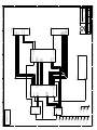
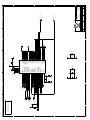
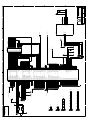
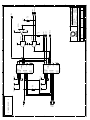
A Schematics
A.1 Mother Board . . . . . . . . . . . . . . . . . . . . . . . . . . . . . . . . . . . . . . .
A.2 nRF2401 Radio Board . . . . . . . . . . . . . . . . . . . . . . . . . . . . . . . . . . .
32
32
42
B Errata
B.1 Post Delivery Modifications . . . . . . . . . . . . . . . . . . . . . . . . . . . . . . .
B.2 Bill of Components . . . . . . . . . . . . . . . . . . . . . . . . . . . . . . . . . . . .
B.3 Schematics . . . . . . . . . . . . . . . . . . . . . . . . . . . . . . . . . . . . . . . . .
43
43
44
44
C FPGA control.c
45
D example.ucf
50
E FPGA Makefile
54
4.4
4.3.4 Direct Mode . . . . . . . . . .
TinyOS . . . . . . . . . . . . . . . . .
4.4.1 Porting TinyOS . . . . . . . .
4.4.2 FPGA, ATMega Interconnect
4.4.3 nRFSPI . . . . . . . . . . . . .
.
.
.
.
.
4
.
.
.
.
.
.
.
.
.
.
.
.
.
.
.
.
.
.
.
.
.
.
.
.
.
.
.
.
.
.
.
.
.
.
.
.
.
.
.
.
.
.
.
.
.
.
.
.
.
.
.
.
.
.
.
.
.
.
.
.
.
.
.
.
.
.
.
.
.
.
.
.
.
.
.
.
.
.
.
.
.
.
.
.
.
.
.
.
.
.
.
.
.
.
.
.
.
.
.
.
.
.
.
.
.
.
.
.
.
.
.
.
.
.
.
.
.
.
.
.
Chapter 1
The Hogthrob Prototype Platform
The Hogthrob prototype platform (HogthrobV0) must serve as a development platform throughout the Hogthrob project. It must be general enough to allow a large variety of configurations
and robust enough to allow lab and field experiments.
The platform was defined by the Hogthrob partners and was implemented by I/O Technologies delivering practical expertise in embedded systems design, PCB1 layout and assembly. The
PCB was manufactured and assembled in a foundry before delivery. In total 50 boards are produced.
The platform was delivered in two stages. First a few boards were delivered for testing
and evaluation. The testing involved developing the software to be run on the platform testing
every feature of the platform. In a second stage the 50 boards are produced.
The design goals of the Hogthrob prototype platform are different from that of the sensor
node we are trying to build. It must be functionally equivalent of our sensor node on a chip,
and we must be able map the design to the performance of a sensor node on a chip.
The two major goal of HogthrobV0 are
• to allow software/hardware co-design
• to provide a prototype platform for further exploration of the design space.
The platform must be flexible enough to let us change any of the givens of the sensor node
design: radio, sensors, microprocessor, hardware accelerators, etc. This allows us to explore a
broad spectrum of design choices: hardware/software boundary, radio protocol design, duty
cycling, sensor sampling frequencies, etc.
To achieve these objectives we adapt a modular design strategy so that we can swap sensors
or radio transceivers with ones resulting in more efficient energy and system performance. To
experiment with microprocessor designs and/or hardware accelerators, we need some form of
reconfigurable logic on the prototype platform. To sum up our strategy for building a platform
with no constraints:
• Configurable logic (FPGA) to develop hardware
• A/D2 converter (rarely included in configurable logic blocks)
1 Printed
2 Analog
Circuitry Board
to digital
5
• A low-power timer
• Add on-board with wireless communication
• Add on-board with sensors
• The ability be battery powered
We choose to implement these goals using a Xilinx Spartan III FPGA with external FLASH
for the FPGA configuration and for the program running on the FPGA. In addition we placed an
ATMega 182l MCU that provides A/D as well as housekeeping for the FPGA power up/down
procedure.
The following Section describes the platform design, pin connections and the general procedure to setup the platform eg. cables, power source, etc. Programming the FPGA is described
in Section 3. Programming the ATMega is described in Section 4.
1.1
Further Information
Apart from this manual the following documents provide further information about the platform:
• Martin Hansen: System Design Specification for 1087 Hogthrob (unpublished)
• Kashif Virk: Testing FPGA Interfaces on Hogthrob Development Platform[4]
6
Chapter 2
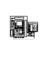
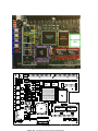
HogthrobV0 Overview
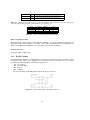
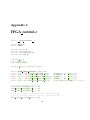
The functionality of the platform can be divided into four closely interacting subsystems: computing, sensing, communication, and power supply (see Figure 2.1). We will look into the details of each of these subsystems in the following, fist let us sum up the contents of this division:
Computing an FPGA for hardware development and an MCU with A/D converter for external
peripherals
Communication an add on-board with a flexible radio with low level access
Sensing an add on-board with sensors
Power a power supply allowing battery powered operation while maintaining a steady supply.
Figure 2.1 depicts each of these subsystems and their interconnection, Figure 2.2 depicts the
layout on the board and external connections.
2.1
External Connections and Cables
HoghtrobV0 has 6 pin headers for external connections:
J1 Combined programming of ATMega and JTAG bus (FPGA, PROMs)
J2 16 general I/O pins for FPGA
J3 ATMega analog input and digital I/O
J4 15 general I/O pins for FPGA
J5 Radio power
J6 Radio I/O
J7 External 5 V power supply (see below for polarity).
2.1.1
Power
The board is powered through a common power connector (see figure 2.3(a)). The input power
may not exceed 5.5 V and it is essential that polarity is not reversed (positive connected to gnd).
If in doubt insert a diode in the power cable to avoid glitches.
7
Mother Board
3.0V Flash
LP2989
Flash Memory
4M x 16 bit
LED’s
Spartan3 XC3S400
S
P
I
PB’s
Serial
PROM 2
Serial
PROM 1
J
T
A
G
nRF2401
PA
U
A
R
T
1
UART2
3.0V Flash
Radio Board
FPGA Core
S
P
I
2.5V
1.2V
MAX 192R
UART2
2.5V
MAX 192R
Program Flash
128 KB
I2C
AVR
Processor
Core
Sensors
A/D
SRAM
4KB
Comp
Sensor
Board
Clock
4MHz
Bus
Exchange
Switches
S
P
I
U
A
R
T
1
Frequency
Synthesizer
U
A
R
T
1
3.0V Analog
Crystal
16MHz
Lowpass Filter
fc=1.5MHz (max)
JTAG
3.0V
LP2989
ATMega 128L
Clock 8MHz
Baseband
Processing
Logic
LNA
Clock
48MHz
PB
LED
2.5V
(Optional)
3.0V
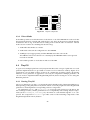
Figure 2.1 HogthrobV0 interconnections (figure by Kashif Virk))
8
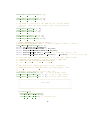
(a) Motherboard (Picture and annotation by Kashif Virk)
9
(b) Layout
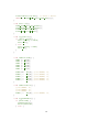
(a) J5 power connector
(b) J1 programming connector
Figure 2.3 Power and programming cables
2.1.2
Programming
Connector J1 combines programming interfaces for the ATMega, FPGA and configuration PROMs
(see figure 2.3(b)). Pin 16 has been cut and pin 16 has been blocked to provide a key for the correct placement of the connector. The two cables are combined into one that is connected to the
appropriated programmers when programming either device.
As depicted in Figure 2.3(b) the FPGA is connected to a Xilinx1 programming dongle, such
as Platform Cable USB or Parallel Cable IV. The ATMega is connected to an Atmel2 programming
dongle such as the STK-500 or AVR-ISP. connected to
JTAG
TDO
TDI
TMS
TCK
V ref
Gnd
2.1.3
HTV0 J1
1: RESET
2: FPGA TDO (JTAG0)
3: 3.0 V
4: TDI (JTAG1)
5: SCK
6: TMS (JTAG2)
7: RXD0/DPI
8: TCK (JTAG3)
9: TXD0/DPO
10: 3.0 V
11: FPGA RX
12: GND
13: FPGA TX
14: GND
15: PEN
16: GND (Pin cut)
STK-500 (ISP)
RST
SCK
MOSI
MISO
GND
(only for SPI protramming)
UART
The ATMega and FPGA have a UART connection to the J1 pin header. The voltage levels of
these connections are different to those of a PC-RS232 UART and requires level conversion to
1 http://www.xilinx.com
2 http://www.atmel.com
10
be connected to a PC.
Some programmer boards such as the Atmel STK-5003 feature built in level conversion,
however using a USB-RS232 converter can be convenient. Such a converter is usually built
using a general purpose serial conversion chip such as Prolific PL-23034 or FTDI FT-2325 , the
inputs on the chip can be connected to the UART output of the platform.
2.2
Pin Connections
End point
J1
J1
J1
J1
LED
Button
2.2.1
Line
SCL
SDA
RXD1
RXD1
LED
BOTTON
DONE (FPGA booted)
ATMega-FPGA
Line
Power on
DONE
FPGA CS
FPGA INT6
ALE
RD N (PROM SEL)
WE N
DA0-DA7
2.2.2
AVR
PD0
PD1
PD2
PD3
PD7
PE7
PB4
AVR
PD6
PB4
PC7
PE6
PG2
PG1
PG0
PA0-PA7
FPGA
High means FPGA on
B14 (VCCAUX DONE)
P7 (B5 IO)
N5 (B5 IO)
T5 (B5 IO
T4 (B5 IO L01P 5/CS B)
T3 (B5 IO L01N 5/RDWR B)
P5, N6, M6, B6, N7, M7, T7, B7
ATMega-Radio
RADIO IO11 used to select RX/TX direction if RXD1 and TXD1 is used as a combined singlewire UART.
3 http://www.atmel.com
4 http://www.prolific.com.tw
5 http://www.ftdichip.com
11
Line
RXD1
TXD1
CLK (SCK)
MOSI+MISO
INT0
Radio Board
J1, pin 31
J1, pin 32
CLK1
DATA
DR2
Radio IO0
Radio IO1
Radio IO2
Radio IO3
Radio IO4
Radio IO5
Radio IO6
Radio IO7
Radio IO8
Radio IO9
Radio IO10
Radio IO11
2.2.3
DR1
DOUT2
CS
PWR UP
J1, pin 13
J1, pin 15
DEVICE CODE0
DEVICE CODE1
LED0
LED1
CLK2
CE
NC7SZ125
AVR
PD2 (RXD1/INT2)
PD3 (TXD1/INT3)
PB1 (CLK)
PB2+PB3
PE4 (INT4)
PE5 (INT5)
ˆ
+ (by mistake) PB0 (SS)
PB5
PB6
PB7
FPGA
FPGA IO17
FPGA IO18
FPGA IO13
FPGA IO14+FPGA IO15
FPGA IO1
FPGA IO4
PD4
PD5
PG3
PG4
PC3
PC2
PC1
PC0
FPGA IO2
FPGA IO3
FPGA IO5
FPGA IO6
FPGA IO7
FPGA IO8
FPGA IO9
FPGA IO10
FPGA IO11
FPGA IO12
FPGA IO0
FPGA IO16
Bus Switches
PI3B16213
RADIO MUXx
AVR - pin
RADIO MUXS2
S2
2
PC6
RADIO MUXS1
S1
1
PC5
12
RADIO MUXS0
S0
0
PC4
2.2.4
FPGA IO
Line
FPGA AIO0
FPGA AIO1
FPGA AIO2
FPGA AIO3
FPGA AIO4
FPGA AIO5
FPGA AIO6
FPGA AIO7
FPGA AIO8
FPGA AIO9
FPGA AIO10
FPGA AIO11
FPGA AIO12
FPGA AIO13
FPGA AIO14
FPGA AIO15
FPGA AIO16
FPGA AIO17
FPGA AIO18
FPGA AIO19
FPGA AIO20
FPGA AIO21
Bank
B6
B6
B6
B6
B6
B6
B6
B6
B6
B6
B6
B6
B6
B6
B6
B6
B6
B6
B6
B6
B6
B6
Pin
K1
R1
P1
P2
N3
N2
N1
M4
M3
M2
M1
L5
L4
L3
L2
K6
K4
K3
K2
J4
J3
J2
Connector
J2, pin 5
J2, pin 7
J2, pin 9
J2, pin 11
J2, pin 15
J2, pin 17
J2, pin 19
J2, pin 21
J2, pin 25
J2, pin 27
J2, pin 29
J2, pin 31
J2, pin 32
J2, pin 30
J2, pin 28
J2, pin 26
J2, pin 22
J2, pin 20
J2, pin 18
J2, pin 16
J2, pin 12
J2, pin 10
Line
FPGA BIO
FPGA BIO1
FPGA BIO2
FPGA BIO3
FPGA BIO4
FPGA BIO5
FPGA BIO6
FPGA BIO7
FPGA BIO8
FPGA BIO9
FPGA BIO10
FPGA BIO11
FPGA BIO12
FPGA BIO13
FPGA BIO14
FPGA BIO15
FPGA BIO16
FPGA BIO17
FPGA BIO18
FPGA BIO19
FPGA BIO20
FPGA AIO21
13
Bank
B7
B7
B7
B7
B7
B7
B7
B7
B7
B7
B7
B7
B7
B7
B7
B7
B7
B7
B7
B7
B7
B7
Pin
G2
C1
R1
C2
C3
D1
D2
F3
D3
F1
F2
F4
F4
F2
F3
G5
F5
G3
G4
H3
H4
H1
Connector
J4, pin 5
J4, pin 7
J4, pin 9
J4, pin 11
J4, pin 15
J4, pin 17
J4, pin 19
J4, pin 21
J4, pin 25
J4, pin 27
J4, pin 29
J4, pin 31
J4, pin 32
J4, pin 30
J4, pin 28
J4, pin 26
J4, pin 22
J4, pin 20
J4, pin 18
J4, pin 16
J4, pin 12
J4, pin 10
Chapter 3
Xilinx FPGA
The FPGA portion of the platform is controlled by the ATMega in a number of ways. The ATMega powers the FPGA on and off and points the radio interface to either the ATMega of FPGA.
The FPGA boot procedure and ATMega dependence is described in Section 4.2 on page 20, the
following describes the features that are independent of the ATMega.
In order to program the FPGA the appropriate compiler must be installed see Section 3.2.
3.1
Hardware Setup
Once the FPGA has been booted it operates independently of the ATMega. It features a large
number of digital I/O lines, buttons, leds, external UART connection and is connected to an
external FLASH. See schematics in Appendix A.
3.1.1
Configuration Flash
On boot the FPGA loads a configuration from the configuration FLASH. The board has one
flash chip mounted and solder pads for an optional additional FLASH chip. Chip selection is
performed by the ATMega (described in Section 4) and is required before booting the FPGA.
The FLASH chip is programmed using Xilinx Impact using the JTAG connector.
3.1.2
Program Flash and ATMega interface
The FPGA is connected to the program flash and ATMega using elaborate interfaces. Using
these interfaces requires including an appropriate controller in the FPGA logic, that we will not
cover here. The detailed FPGA testing procedure?? describes an example of such controllers.
The FGPA is connected to the ATMega by a set of pins that can be treated as either general
purpose I/O pins or as external memory to the ATMega. This interface uses a set of pins to
alternate between address and data, this is controlled automatically by the ATMega, but must
be programmed accordingly on the FPGA.
Programs for the CPU running on the FPGA can be stored either in block-memory or via
the external FLASH. This requires that the FPGA implements a FLASH controller for storing an
retrieving data from the FLASH.
14
3.1.3
Clock Source
The FPGA has two external crystal clock sources: a 4 MHz and a 48 MHz source. The 4 MHz
clock is always enabled, but the 48 MHz must be enabled by pulling I/O pin R10 high.
3.1.4
FPGA I/O
A large number of the FPGA I/O pins have been connected to external connectors either with
a dedicated purpose of as general purpose I/O. An example constrains file with appropriate
naming for the external I/O pins is given in Appendix D on page 50, as well as [4].
Each of the FPGA I/O blocks must be supplied with an external power source. The blocks
B0, B1, B2, B3, B4 and B5 (that are used internally on the board) are all supplied on the board
while B6 and B7 must be feed through the connectors J2 and J4 respectively using a jumper.
Block
Power
Connection
B0
Internal (3.0 V)
FLASH
B1
Internal (3.0 V)
FLASH
B2
Internal (3.0 V)
FLASH + FPGA UART (connector J1)
B3
Internal (3.0 V)
Radio via J6
B4
Internal (2.5 V)
Buttons + LEDs
B5
Internal (3.0 V)
ATMega
B6
External through pin 3 of J2
J2
B7
External through pin 3 of J4
J4
B8
Grounded
Buttons and Leds
The FPGA is connected to 3 buttons and 3 leds, the LEDs are active high, while the buttons are
low when pressed. Please note this is a different semantics than other buttons and leds found
on the board. See Chapter 4.
FPGA UART
The FPGA has two pins connected to the common programming connector J1 intended for use
as a UART. The two pins are F14 and F15, these pins are part of the I/O block B2 resulting in an
3.0 V level on these two pins.
3.2
Software installation
To program the FPGA the ISE tool-suit from Xilinx is required. A full version supporting all
Xilinx devices or a limited “WebPack” version only supporting smaller devices can be downloaded. The WebPack should be sufficient for our device.
ISE WebPack is free of charge, but you are required to register with Xilinx in order to download it. At the time of writing the latest version (8.1i) is available for Windows, Linux and
Solaris. The Windows is self explanatory, while the Linux installtion can be a bit tricky.
3.2.1
ISE 8.1 for Linux
Use the provided installer (either web-install or full download), this will provide you with a
Xilinx directory containing the tools. The installer also compiles and installs drivers, which
15
requires you to run the installer as root.
The installer is provided for Red Hat Linux, but it should work perfectly on most other
distributions, except for the driver setup scripts. The installer contains scripts to setup the
drivers at boot time and these are unlikely to be setup correctly outside of Red Hat.
The installation script will also prepare an environment settings that you will need to load
to start the tools. Depending on your shell this will look something like this:
source ˜/Xilinx/setting.sh
USB Cable Drivers
The drivers provided by Xilinx at the time of writing only support Linux kernel version prior
to 2.6.13. For more recent kernel versions you need to obtain one driver from from Jungo.com
directly and one from the Xilinx distribution.
For recent kernel versions get the “driver development kit” and compile this. For gcc versions 4.0 and up find the macro “KBUILD STR” in the Makefile and remove it.
tar zxfv WD802ln.tgz
cd WinDriver/redist
./configure --with-kernel-source=/usr/src/linux-headers-2.6.15-26-386
make
For udev enabled platforms a udev rule must be created for the driver to be loaded. Create
a udev rule in /etc/udev/rules.d for example 10-xilinx.rules
BUS=="usb", SYSFS{idVendor}=="03fd", SYSFS{idProduct}=="0007",\\
RUN+="/sbin/fxload -v -t fx2 -I /usr/local/Xilinx/bin/lin/xusbdfwu.hex
Parallel Cable Drivers
The drivers for the parallel and USB cables are installed as part of the installation procedure.
If this should fail or if you upgrade your kernel you can download the drivers from one of the
following locations depending on your kernel version. Unpack theses archives and build the
drivers with make:
ftp://ftp.xilinx.com/pub/utilities/fpga/linuxdrivers.tar.gz
For Linux 2.6
ftp://ftp.xilinx.com/pub/utilities/M1_workstation/linuxdrivers.2.6.tar.gz
The driver installation creates two scripts to load the drivers and setup the required device
nodes. However the permissions of these device nodes are set such that only root can access the
cables.
/lib/modules/misc/install_windrvr6 windrvr6
/lib/modules/misc/install_xpc4drvr
chmod 777 /dev/xpc4* /dev/windrvr6
Pace
Pace (the constraints editor) as of version 8.1i unfortunately suffers from a few quirks that need
to be taken into account. First of all make sure that the library libmotif3 is install, secondly
make sure to setup your DISPLAY DISPLAY=:0
16
3.2.2
ModelSim
In addition to ISE it might be useful to simulate a project for debugging. For this purpose Xilinx
provides ModelSim Xilinx Edition-III free of charge1 .
Don’t forget to select the free ”Starter” version when installing. And be sure to select VHDL
and not Verilog. The license file is then requested with a web link in the start menu.
3.3
Building a Project
Building the project can be built using the Xilinx ISE graphical environment or it can be built
using the corresponding command line tools. Either way the two methods go through the same
steps. An example make file has been provided as Appendix E.
Along with the platform two example projects have been provided: An 8051 core Oregano
and an AVR core Nimbus
3.3.1
Oregano
Oregano is an open source, freely available 8051 core2 adapted to the Xilinx environment. It is
a straight forward 8051 implementation with a few external peripherals such as UART.
Boot Loading Programs
Provided with the Oregano 8051 is a boot loader example design (RAMLOAD) this program
accepts programs from the UART and stores them in the code memory space of the 8051. This
boot loader resides in the internal memory (ROM) of the 8051 and is booted as the first program.
At start-up the boot loader emits a “=” and expects a program to be uploaded once the
upload is complete it emits a “:” and waits for a command to start executing further[1].
Send a “/2000” to start the program at address 2000
If the address is accepted it sends a “@” before jumping to the address
Uploading Programs
Building programs for oregano is the same as for any other 8051 core. Compile the program
using an 8051 compiler such as Keil PK513 and upload the program to the FPGA board using
the UART:
cat hathat.hex > /dev/ttyUSB0
echo -en "/2000\r" > /dev/ttyUSB0
1 http://www.xilinx.com/ise/optional
prod/mxe.htm
2 http://www.oregano.at/
3 http://www.keil.com
17
Chapter 4
ATMega
In this section we will concern our selves with programming the features of the HTV0 board
dealing with the ATMega. We will present programs them in C (see Appendix C) and construct
TinyOS interface to control the features (see Section 4.4).
4.1
Hardware Setup
The ATMega is powered on and boots a program from FLASH as soon as the board is powered
up. It is then up to the ATMega program to turn on a, power up the FPGA and so forth.
The ATMega execution is controlled by a set of fuses before booting the first program these
fuses must be set to match the configuration of the chip.
4.1.1
Fuses
The internal fuses of the ATMega change certain properties of the ATMega: available clock
sources, external interfaces (ISP, JTAG, etc.), and more. These settings are pre-programmed and
cannot be altered by the ATMega. Besides controlling the functionality of the ATMega, the
fuse settings can affect power consumption. In our case the FPGA is by far going to be the
dominating factor, making this aspect less important. Consider for example the JTAG interface
(on port-F) - this peripheral could be disabled to make sure that is does not consume any power,
on the other hand we are not sure how this platform is going to be used, so disabling JTAG
might be a problem.
A set of fuse settings is provided in Table 4.1 that enables most features, sets up clock sources,
brownout detection, etc. The setting are programmed using AVR Studio for Windows or using
uisp:
uisp -dserial=/dev/ttyUSB0 -dpart=ATmega128 -dprog=stk500
--wr fuse l=0x8e --wr fuse h=0x00 --wr fuse e=0xff
4.1.2
ATMega I/O
In addition to the control pins for the FPGA, the A/D pins of the ATMega are connected to the
J3 pin header. Furthermore the ATMega is connected to a LED and a button.
See schematic in Appendix A for further information.
18
Extended fuse
High fuse
0xFF
0x00
0x8E
Low fuse
M103C OFF, WDTON OFF
OCDEN ON, JTAGEN ON, SPIEN ON, CKOPT ON,
EESAVE ON, BOOTSZ1 ON, BOOTSZ0 ON, BOOTRST OFF
BODLEVEL OFF, BODEN ON, SUT1 ON, SUT0 ON
CKSEL3 OFF, CKSEL2 OFF, CKSEL1 OFF, CKSEL0 ON
Table 4.1 ATMega fuse settings (see [2, p.289] for further). The semantics of the fuse settings are
reversed, meaning that a logical 1 corresponds to “off” and 0 to “on”.
Location
Radio
Radio
Motherboard
Motherboard
Component
D1
D2
D1
B4
AVR pin
PC3
PG4
PD7
PE7
Active
Low
Low
High
High = pressed
Table 4.2 LEDs on the motherboard and radioboard
Button and LED Interface
The platform provides 3 LEDs connected to the ATMega: one on the motherboard and two on
the radio-board. The semantics of the LEDs on the radio and motherboard are different (see
Table 4.2). In addition the B4 button is connected to the external interrupt 7.
External Interfaces
Analog, UART1/UART2, ISP
4.1.3
Radio Control
Selecting whether the FPGA or the ATMega uses the radio is done by two bus switches. These
connect the radio either to the ATMega or to the FPGA. The two switches act as a cross-bar
switch interconnecting either of 4 buses (see Figure 4.1):
A1 reset-value
A2 the radio (RF)
B1 FPGA
B2 ATMega
The relevant states of the MUX interconnect the buses as follows:
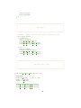
Figure 4.1 Bus switches (Figure by Martin Hansen)
19
cc
V
cc
co
V
O
n
V
DC−
DC
ATMega
FPGA
Figure 4.2 FPGA to ATMega interconnect. Each I/O pin of the FPGA is connected with two diodes
for Electro-Static Discharge protection[5].
RF-AVR (1):
RF-FPGA (2):
A2-B2, A1-B1 RF(A2) to AVR (B2),
Reset(A1) to FPGA(B1)
A2-B1, A1-B2 RF(A2) to FPGA(B1),
Reset(A1) to AVR(B2)
The bus switches are controlled using 3 lines (RADIO MUX0/1/2) connected to AVR pins
PC4/PC5/PC6. The two states are selected are selected as follows:
PC6
2
1
1
AVR pin
RADIO MUX Sx
RF-AVR (1):
RF-FPGA (2):
4.2
PC5
1
1
1
PC4
0
0
1
FPGA Interface
The ATMega and FPGA are interconnected with the external memory interface of the ATMega
and a few control signals. The external memory interface must be configured and enabled from
the ATMega in order to be functional (see below).
As described earlier the ATMega is responsible for booting and selecting a configuration
ROM for the FPGA. Let’s go over the steps to boot the FPGA.
4.2.1
FPGA Power Control
The power supply to the FPGA is controlled by the ATMega. This means that in order to be
functional it must first be powered up. Furthermore great care must be employed regarding the
state of the interconnect-signals when the FPGA is powered off in order to prevent the FPGA
from shorting the pins of the FPGA to ATMega interface to ground.
The internal circuitry of the FPGA requires that all pins connecting the FPGA and ATMega
must be tri-stated (configured as input) when powering the FPGA off (see Figure 4.2).
When the On signal is disabled the supply voltage of the FPGA is connected to ground. If any
of the pins of the ATMega are driving the line (that is configured as output) a direct connection
from supply to ground has been created. This connection will draw a current and in worst case
overloading and destroying the FPGA. It is thus essential that the pins of the ATMega is put
into a state where they are unable to drive a current over the line (tri-stated).
4.2.2
FPGA Control Lines
The FPGA control is performed by the following lines, in short the FPGA has to be supplied
with power and a prom in order to boot. The prom selection logic is probably broken and even
20
MCUCR
XMCRA
XMCRB
// 32
MCUCR
&= ˜_BV(SRW10); // No wait-states
= 0; // No wait-states
= _BV(XMBK) | _BV(XMM0) | _BV(XMM1) |_BV(XMM2);
kB address space w. bus-keeper
|= _BV(SRE); // Enable external mem
Figure 4.3 Configure and enable external memory
if two proms are mounted it will probably not be possible to select the 2nd prom. In any case
the line will be controlled by a pull-up resistor and leaving it will select the available PROM. In
the following we will describe how to turn the FPGA on and off see Appendix C for examples
in C.
In addition to the control lines below the interface also contain the data and address (DA)
lines:
ALE, RD N, WE N External memory interface of the ATMega. This must be enabled to be
functional (see above).
PROM SEL RD N (on the ATMega) doubles as PROM SEL which selects which PROM to use
during start-up of the FPGA. This signal should be pulled low to enable the PROM that is
mounted on all boards. Even if the other PROM is mounted it might still not be possible
to select it (see Appendix B).
FPGA CS is general purpose I/O pin despite the name.
FPGA DONE reports the successful start-up and loading of a configuration from a PROM. If
the PROMS are empty the DONE signal will not be generated. Meaning that the ATMega
cannot wait for the DONE signal if the PROM is empty!
power on Powers up the FPGA by turning on the voltage converters for the FPGA.
FPGA Power On Procedure
Booting the FPGA is done by: (optionally) pulling PROM SEL high, i) pulling power on high.
This causes the FPGA to turn on and load a configuration from the selected PROM. If this is
successful the FPGA will set FPGA DONE high.
FPGA Power On Procedure
Turning off the FPGA is done by first setting the interface pins to input and then powering off
the device. If the external memory interface is enabled the pin direction is controlled by this
unit and external memory must be disabled.
To power off: i) disable external memory ii) set all lines as input iii) set power on low.
Enabling External Memory
The external memory of the ATMega must be configured and enabled for this peripheral unit
within the ATMega to be operational. In addition the FPGA must contain a corresponding logic
block. See Figure 4.3) for a C example.
21
typedef struct \{
unsigned int
rx_en
: 1;
unsigned int
rf_ch
: 7;
unsigned int
rf_pwr : 2;
unsigned int
xo_f
: 3;
unsigned int
rfdr_sb : 1;
unsigned int
cm
: 1;
unsigned int
rx2_en : 1;
//high order bits
\} __attribute__ ((packed))
typedef struct
gen_config_t general_config;
unsigned int
crc_en:1;
unsigned int
crc_l:1;
unsigned int
addr_w:6;
uint8_t
addr1[5];
uint8_t
addr2[5];
uint8_t
data1_w;
uint8_t
data2_w;
//uint8_t
test[3];
// High order bits
__attribute__ ((packed))
//
//
//
//
//
//
//
RX or TX operation
Channel frequency
RF output power
Crystal frequency
RF data rate (1Mbps requires 16 MHz crystal)
Communicaton mode (Direct or ShockBurst)
Enable two channel receive mode
gen_config_t;
//
//
//
//
//
//
//
Enable on-chip CRC generation/checking
8 or 16 bit CRC
Number of address bits (both RX channels)
Up to 5 byte address for RX channel 1
Up to 5 byte address for RX channel 2
Length of data payload RX channel 1 (bits)
Length of data payload RX channel 2 (bits)
// reserved for testing - no need to send
shock_conf_t;
Figure 4.4 Configuration words for nRF2401. The upper part show the general configuration word
the lower shows the additional options for shockburst mode.
4.3
Radio Interface
The radio is connected to ATMega through a digital bus (SPI) that is used both when using the
built in MAC layer of the radio (burst mode) or when transmitting bits directly (direct mode).
In either mode the configuration details of the nRF2401 is setup by uploading a configuration
(or control word) to the device (see Figure 4.4). The configuration sets parameters such as
receive/transmit mode, data-rate, etc. The control word is split in two parts one common part
for direct-mode and ShockBurst and one only required for ShockBurst.
In the following we describe how to control the bus and how to setup the various modes of
operation.
4.3.1
Mastering SPI
Communicating with the nRF2401 takes place over a three-wire serial interface not unlike SPI.
The ATMega128l does not have such a peripheral, but the SPI unit is close enough to be useful.
In order to use the SPI peripheral of the ATMega128l it has to be misused slightly. The
SPI interface is a four wire interface consisting of: chip select (CS), clock (CLK), master send
(MOSI1 ) and slave send (MISO2 ). At each clock tick on the CLK line 2 bits are exchanged: one
on the MOSI line and one on the MISO line. The ATMega128l has one register for each of these
1 Master
2 Master
Output Slave Input
Input Slave Output
22
lines — one outbound register and one inbound register. A transmission is initiated by putting
a byte in the outbound register, starting the clock generator. Once the transmission is over the
received data will reside in the inbound register.
In our case, the MOSI and MISO lines are combined since we never receive data from and
transmit data to the nRF2401 the same time. However it is still possible to utilize the SPI interface of the ATMega128l. Sending works as described above, but in order to receive data from
the nRF2401 we need the ATMega128l to start generating a clock without interfering with the
signal from nRF2401. To do this we start the transmission of the byte “0x00”. Once the transmission of the “0x00” byte is completed, the value from the nRF2401 has been shifted into the
inbound register.
The SPI peripheral can be operated either in a polling mode or using interrupts. Using the
method above complicates the interrupt handling. Usually an interrupt is generated when a
transmission is complete, however when we are trying to clock data out of the nRF2401 this
must be handled properly.
The nRFSPI abstracts the bit level operations of communicating with the nRF2401, but allows full flexibility. ShockBurst and direct-mode operations communication is possible using
this component.
4.3.2
SPI Master Mode and PB0
ˆ not slave select) is connected to DR1 in the final platform, PB0 will be lifted
By mistake, PB0 (SS
off the board and, thus, be completely irrelevant, however in the following we describe the
consequences of this mistake.
The DR1 signal is driven by the nRF2401 and the SPI peripheral of the ATMega is influenced
by the state of this signal - particularly in SPI master mode. When communicating over the SPI
bus the master shall generate a clock signal. The nRF2401 does not have a clock generator for
this signal, thus the ATMega will always be designated as the master.
For the short burst mode, DR1 will toggle when data is ready. In direct mode, DR1 will be
pulled low. For master mode of SPI peripheral, both of these are wrong. In the master mode,
ˆ is disregarded only if this is set to output (see [2, p.166]) - in this case both the ATMega and
SS
nRF2401 will attempt to drive the line. If PB0 is set as input (still, while the SPI is in the master
mode) PB0 must be held high by an external source for the SPI bus to operate, which we cannot
guarantee is performed by the nRF2401.
ˆ value.
It is, thus, important that we are able to ignore the SS
4.3.3
ShockBurst Mode
The Shock Burst mode provides a built in CRC check, MAC protocol, etc.The radio control data
and data packet are sent via SPI.
Shock burst is enabled by uploading a special configuration word to the device (see Figure 4.4). From here on the radio handles the address match and CRC check and only returns
valid packets. A shock burst TX could look like this:
1. AVR enbles the SPI bus as a master
2. AVR powers up the radio and waits for it to be ready
3. AVR sends a shock burst mode configuration to the nRF2401
4. AVR sends a packet with packet header to nRF2401
23
sendShockConfig
rxMode
txMode
sendPkt
samplePort
dataReady
HPLADC
set
fired
HPLUART
nRFSPI
buttonInterrupt
FPGAInterrupt
sendDone
dataReady
Application
htV0Control
FPGASelProm
FPGAPowerDown
FPGAPowerOn
radioMuxToAVR
radioMuxToFPGA
enableButtonInt
disableButtonInt
FPGAFlashBootOK
get
get
print
send StdOut
On
Off
Timer
LED’s
Figure 4.5 TinyOS components
4.3.4
Direct Mode
It should be possible to use the SPI unit to clock data in or out of the nRF2401. In order to do this
the bit stream must be constant and without jitter. Any holes in the stream would be directly
translated to the air. Eg. if the SPI unit is waiting for more bit the radio would stall. A direct
mode session would look something like the following:
1. AVR enbles the SPI bus as a master
2. AVR sends a direct mode configuration to the nRF2401
3. AVR flips CE, CS appropriately and the nRF2401 enters the active mode
The PB0 line will now be driven low constantly by the nRF2401 and has to be ignored.
For both Tx and RX
4. It should be possible to clock data in and out of the nRF.
4.4
TinyOS
To span across multiple platforms easily TinyOS introduces the concept of platforms. For each
platform implementations are provided for certain low-level interfaces used by higher level
applications (one can think of these as drivers in a traditional operating system). By sharing
interfaces across platforms an application can easily be compiled for multiple platforms. In
our case we have implemented the HogthrobV0 platform, but for testing we are also using the
BTnode2 platform.
4.4.1
Porting TinyOS
The core of TinyOS is very slim — it contains the simple thread model of TinyOS and little more.
Subsequently, porting TinyOS is trivial, but in order to access the peripherals of the HogthrobV0
platform we must implement corresponding software components.
We implement nRFSPI and htV0Control to access the radio transceiver, the FPGA, the
bus-exchange switches, and the push-buttons. For compatibility with existing TinyOS components (such as IntOutput, IntDebug, etc.) the LEDs are controlled through the Leds component. The component htV0Control provides control of the remaining components of the
HogthrobV0 platform: FPGA, buttons.
24
In addition to this the ATMega128l based Mica variants and BTNode2 share the common
meta platform avrmote — this platform provides only functionality related to the ATMega128l.
The HogthrobV0 shares the same processor and we reuse as many components as possible.
4.4.2
FPGA, ATMega Interconnect
The FPGA is connected to the ATMega128l through the external memory interface — from the
ATMega the FPGA is merely memory mapped to a special portion of memory.
The htV0Control components contains abstractions to enable and disable the external
memory interface. In addition to the memory interface the two are connected with an interrupt line from the FPGA to the ATMega128l, htV0Control provides a TinyOS event for this
interrupt.
This component alone does not provide the means for communicating between a processor core in the FPGA and the ATMega128l. This will have to be constructed as an additional
component.
4.4.3
nRFSPI
The nRFSPI component work as a wrapper for the functionality of the nRF2401 and provides
a packet level interface to the byte level SPI peripheral of the ATMega128l. The component is
shared among the platforms that we are working with (BTNode2 and HogthrobV0). The nRFSPI component is not a MAC, it assists in communicating with the nRF2401, but does not handle collisions and retransmissions or any other facilities that one would expect from a MAC.
Furthermore, it does not handle the timing required when switching operation mode of the
nRF2401, this will have to be implemented in an additional component.
The interface of nRFSPI abstracts the access of the nRF2401 by providing events and commands for common operations and providing data structures with human readable field names.
The interface is shown in Figure 4.6 and the two data structures used by the interface is shown
in Figure 4.7.
TinyOS does not provide any form of memory management. This means that the programs
will have to keep track of the used and available space. The two common approaches to this in
TinyOS are transfer of ownership and buffer trading[3]. Transfer of ownership implicitly transfers
the ownership of a buffer when it is passed from component to component. It is up to the components to ensure that only the right one modifies it at the right time. Buffer trading denotes the
process of giving a buffer to a component and getting one back. Using the data structures enables the buffer trading type of memory management — trading chunks of equal size. The two
types of memory management are not mutually exclusive and can be used to the convenience
of the programmer.
In the nRFSPI interface the event dataReady is an example of buffer trading while rxMode
is an example of transfer of ownership.
25
interface nRFSPI {
command void enableSPIMaster();
/* Set up the nRF2401 in rx mode and provide a buffer for reception
* The buffer must be atleast as big as ADDR_LEN and PAYLOAD_LEN
*
* The buffer is given back when the radio is set to txMode
*/
command void rxMode(nRF_pkt_t* pkt);
/* Set the nRF2401 in tx mode and give back a buffer given in rxMode
* of NULL if no buffer was given.
*/
command nRF_pkt_t* txMode();
/* Send a payload of "pkt" to the recipent in "pkt".
*
* @return SUCCESS if no byte were in transit or a buffer
was available.
*
*/
command result_t sendPkt(nRF_pkt_t *pkt);
command result_t sendShockConf(shock_conf_t *conf);
command result_t sendBytesRev(uint8_t *first, uint8_t *last);
async event result_t sendDone();
/* Propagates data from the air to an application.
* channel dennotes the transmission channel (1 or 2)
* last signals the end of the current packet (DR1/DR2 low)
*/
async event nRF_pkt_t* dataReady(uint8_t channel, nRF_pkt_t* pkt);
/* Non-interrupt controlled interface */
command void send_sync(uint8_t data);
Figure 4.6 The TinyOS interface of nRFSPI
typedef struct {
uint8_t payload[PAYLOAD_LEN];
uint8_t addr[ADDR_LEN];
}__attribute__((packed))nRF_pkt_t;
typedef struct {
unsigned int
rx_en
unsigned int
rf_ch
unsigned int
rf_pwr
unsigned int
xo_f
unsigned int
rfdr_sb
unsigned int
cm
unsigned int
rx2_en
//high order bits
} __attribute__ ((packed))
(a) Data packet structure
:
:
:
:
:
:
:
1;
7;
2;
3;
1;
1;
1;
//
//
//
//
//
//
//
RX or TX operation
Channel frequency
RF output power
Crystal frequency
RF data rate
Direct/ShockBurst
Two channel receive
gen_config_t;
(b) Common configuration structure
Figure 4.7 Two data structures for the nRFSPI interface.
26
Chapter 5
Testing
The goal of the following tests is to ensure that all the external interfaces (pin headers) and the
on-board connections to the LED’s, Push Buttons, and all the chip-to-chip interfaces are working properly. The tests are to be performed one time only for each board ensuring a uniform
assurance for each board. We will focus on the chip-to-chip interfaces and assume that unless
we detect errors with the following tests the components are working.
We will be assuming that no X-ray of the board will be performed meaning that there might
be short circuits on the boards that we need to detect. However, such a short could be on the
pins not connected to the pin headers or other chips. We will not be able to detect such errors
and they will not influence the functionality of the platform.
Furthermore the tests are going to ensure that component mounting was accurate, and that
no mistakes were made during post production modifications.
In the following we will describe the ATMega tests in detail and briefly cover the FPGA
testing (FPGA testing is covered in detail in [4]).
5.1
AVR Testing
The test programs for the AVR will be written in the TinyOS and shared via the subversion
repository at: https://svn.hogthrob.dk. If possible, the tests will be carried out using the onboard LED’s and Push-Buttons. Before the test is started, the fuses MUST be programmed.
The upload port of the AVR will be tested first by uploading and downloading test patterns
to the flash. Each of the following tests will be carried out by a single program uploaded to the
AVR. The tests are carried out by connecting the board to a terminal emulator on a PC via the
serial interface and an RS232 level-converter.
The tests are:
Echo Echo the typed character back to the user.
LED Turn the LEDs on motherboard and radio-board.
Button Notify a Push-Button press to the UART
ADC Print the value of the ADC to the UART
FPGA↔AVR Write patterns to the entire address space of the interface and report status via
the UART
27
nRF2400 Set one node as RX and one as TX and try to make them communicate
The tests should be performed in the following order:
The test sets the Bus-Switches (MUX) to point towards the AVR at boot-up. If this fails, the
UART1 LED’s will not function.
5.1.1
Fuse programming
The fuse setup particular features of the ATMega (see section 4.1.1).
1. Use UISP to program fuses
5.1.2
Program upload
Test the program upload port (AVR-UART0, AVR→PEN).
1. Test that the PEN (program enable) and the UART0 (RXD0/RXD1) pins are connected and
working.
2. Connect the HoghthrobV0 comm port to the STK500 ISP.
3. Upload anything to the Flash and read it back using USIP (on Linux) The test patterns are:
0’s, 1’s and alternating 1’s and 0’s.
4. The uploaded and the downloaded programs should be the same.
A simple way to test this is simply to test this is to supply uisp with the “–verify” option:
uisp --verify -dprog=stk500 -dserial=/dev/ttyUSB0 -dpart=ATmega128 -v=2 --erase
--upload if=build/hogthrobV0/main.srecb
5.1.3
ATMega UART1
Test the connection to the secondary UART (AVR-UART1)
1. Test that the Rx and the Tx lines are connected to the Pin Header (Radio IO). Test the
buffer (NC7SX125) and the control line (Radio IO11 → PC11)
2. Connect RXD1/TXD1 on the Radio Connector to the PC via RS232 level- converter (on
STK500). Upload the test program to the AVR. Start MiniCom terminal emulator on PC
(with Linux) or a similar program with Windows (Hyperterminal). Local echo should be
disabled in the terminal emulator. The control line for NC7SX125 is set ’High’ and the
resistor R37 is unmounted (if mounted).
3. Each typed character should be echoed back immediately.
5.1.4
ATMega LED
Test connection to LEDs (D0 on motherboard and D0/D1 on radio board)
1. Test that the LED’s on the MB (LED → PD7) and on the Radio Board (RADIO IO7/RADIO IO8
→ PC3/PG4) are working
2. Start the blink test in the test program
3. See the LED’s blinking
28
5.1.5
ATMega push-buttons
Test the ATMega push button (AVR - Push-Button).
1. Test that the on-board Push-Button is connected to the AVR (PE7)
2. Upload the test program (the Push-Button test is enabled by default)
3. For each Push-Button press, the UART should report this.
5.1.6
ATMega radio connection and bus switches
Test connection to the radio, this connection goes through the bus switches (AVR-nRF). Test that
the Radio Transceiver is able to communicate through the connector to the Radio Board. Test
the MUX and the MUX-control lines (RADIO MUX0/1/2 → PC4/PC5/PC6).
1. Use 2 nodes. Connect the Radio Boards to the MB. Upload the test program.
2. The test program has a one-way test (the receiver tests the CRC). It sets the the MUX to
connect the radio and the AVR. Start by enabling one as an RX, and then enable the other
as a TX
3. As soon as the TX-node is enabled, the RX-node should start blinking the LED’s and print
status on the terminal.
5.1.7
ATMega sensor connector
Test the external sensor connections. These connection can function either as analog or digital,
we only test their analog mode.
1. Test that the ADC0-ADC7 connections to J3 are working properly.
2. Connect all the sensors to ground (pin 1-8 to pin 15) and to AREF reference voltage (pin
1-8 to pin 9), respectively.
3. Start the ADC printer on the node
4. With ADC input grounded, all should be 0 and with all set to AREV they should be
0xFFFF.
5.2
FPGA Testing
The FPGA will be tested using a simple VHDL state machine. This state machine will input
and output some registers - continuously stimulating the inputs and the outputs. The tests
will be carried out using the on-board LED’s and connecting a logic-analyzer and capturing the
waveforms. The Logic Analyzer can be replaced with the Xilinx ChipScope. FPGA testing is
further documented in [4].
Required Programs:
AVR FPGA-bootup-and-MUX-selector, memory write-read-back-test
FPGA Xilinx ChipScope core, AVR-SRAM interface, FPGA→FLASH interface
29
5.2.1
PROM Programming (Upload)
Test JTAG and PROM-lines.
1. Connect JTAG and upload a configuration.
2. Read it back and see that the two are the same.
5.2.2
FPGA Boot (FPGA control-lines)
Test that the FPGA↔AVR control-lines are correct and that the FPGA boots.
1. Upload the AVR program.
2. AVR sets the correct PROM () and powers up the FPGA (power on) - FPGA loads the
program from the PROM. Set PROM SEL (It will be pulled-up now) AVR wait for the
DONE Signal. Turn on the LED’s.
3. After applying power, the AVR-connected LED (on the MB) should turn on after ”a while”.
5.2.3
FPGA→LED, Push-Button
1. Test the LED and the Push-Button connections using the Xilinx ChipScope
2. Upload FPGA configuration and set the LED values in the ChipScope. Toggle the Push
Buttons and see the changes.
5.2.4
FPGA→Sensor Board (Digital Connectors), FPGA→nRF, FPGA→UART
(Serial Interface)
All of the following tests can be performed either manually using the Xilinx ChipScope or by
writing a simple FPGA configuration that automates the procedure.
1. Test that the connections to the pin headers are working correctly using the Xilinx ChipScope.
Connect both the Digital Connectors with each other (J4 to J5).
If the Radio Transceiver is working with the AVR, we just need to test that the FPGA connections to the Radio Connector are working. Connect the pins on J1: 1,3,5,7,9,11,13,15→17,19,21,23,25,27,29
After booting the FPGA, the AVR sets the MUX and the Tri-State Buffer.
Short circuit Rx and Tx. Use the Xilinx ChipScope such that whatever you send, you get
back.
2. Upload FPGA configuration with the Xilinx ChipScope. Generate test patterns on each of
the I/O pin groups and check that they show up at the inputs. The patterns include 0’s,
1’s and alternating 1 and 0.
See that the pattern from J4 shows up at J4, Rx→Tx and the J1 pin groups.
To test the LED’s, toggle the values in the Xilinx ChipScope
30
5.2.5
AVR→FPGA
Test that all the data and the control lines are working and that the FPGA can interrupt the AVR.
The FPGA is connected to the AVR using the external SRAM interface (p. 26 in the AVR data
sheet). Reading and writing to a register in the FPGA will test all the pins (AD, ALE, RD N,
WE N). The latch and the register are implemented in the FPGA and the AVR writes and reads
this register.
Since only the lower 8 bits of the address are connected, the high bits of the address space
must be disabled by setting XMM0=XMM1=XMM2=1. The XMEM interface will be configured
to no wait-states, XMCRA=SRW10=0. The bus-keeper is enabled by setting XMBK=1.The external memory interface is enabled by setting SRE in MCUCR.
The FPGA is memory-mapped to the addresses 0x1100-0x90FF (both inclusive). The test
program will write and read back a series of patterns (0’s, 1’s and alternating ’1’ and ’0’).
FPGA CS is untested!!
1. Upload the test program.
2. Boot the FPGA and wait for the DONE signal.
3. Start the test program and wait for it to report success or failure.
5.2.6
FPGA→FLASH
Make sure that the connection to the on-board flash is working. We don’t need to test that the
FLASH is working. The FPGA implements a simple serial interface to the flash and uploads
some data and tries to read it back.
1. Try all 1’s and all 0’s, and alternating 1’s and 0’s.
31
Appendix A
Schematics
32
?
?
?
?
?
?
+5@ ?
+5@ ?
+5@ ?
+5@ ?
'
!
7
>
1
<+
@A
.
F8
:"":+
:"":+@F8 C'( D
,8)8"
.
@A
?
?
?
,B '; 5
,8)8" "B '; 5:
58+
) 2
95< @"B
95< @,B
%" <C'( D
&
&
<+
%" <C'( D
:"":+@F8 C'( D
"
"
A
7F
@ &
,B '; 5
"B '; 5:
58+
F8
:"":+
,8)8"
7F
,
,
) 2
:)
):
,B
"B
+"C'( D
:@ :C'( D
:@ HBC'( D
G8@+
, @+
F8
C'(>D
95< @ +"1
95< @ )
:+8
+C'( D
) F
)
C'(>D
A
@ &
C'(>D
+C'( D
C'(>D
5
5
A
@ &
&
B &E A
&
%" <C'( D
95< @"B
95< @,B
G8@+
, @+
F8
C'(>D
95< @ +"1
95< @ )
:+8
:"":+@F8 C'( D
B &E A
D
D
95< @ :C'( 7D
95< @ :C'(
95< @ :C'(
D
D
+"C'( D
,
:@ :C'( D
,
:@ HBC'( D
95< @ :C'( 7D
95< @ :C'(
95< @ :C'(
,
,
C'(>D
& @
&&
&&
(
&&
( "
9 +
)*
"
@
(
#$ % &
& +
) 2
:)
):
,B
"B
+"C'( D
,
:@ :C'( D
,
:@ HBC'( D
95< @ :C'( 7D
@
& @
D
8E
D
95< @ :C'(
&&
95< @ :C'(
)
+C'( D
) F
8E
'$ ''
&
8& &
?
&
&
? 4
&
)
%
& / 0 1$
23 '' / #
&
4
5 & ( 6
1 77 ''
:"
;)
& #
&
&
&
.
!
, -
<=
- 01
237 ' 8 =
&
4
6 7> 7'>'
) F
)
?'/
, 1
2
, >
2
:+8
95< @ +"1
:"":+
+"C'( D
+C'( D
,
,
,
,
,
,
A
:@ :
:@ :
,B
:@ :
:@ :
:@ :
) 2
@ &
F8
"B
:)
):
:@ :'
,B '; 5
"B '; 5:
,8)8"
58+
<+
A9
<+
?'/
7?''''
B
+'
+
+"'
+"
*
>
9
<+
A9
1
>
7
!
'
1
>
'
1
>
7
!
'
<+
"
7
''&9
" F
B" F
7F37
5 ' I) F; +"'J
5
I) ; +" J
5
I,B ; +" J
5
I"B ; +" J
5
I
J
5
IB 2 J
5 1 I" J
5 > I" J
J
I,B ';5 J
I"B ';5 :J
IB 2'; +'J
I:
; + J
I:
; +" J
I:
; +" J
I" ; +"1J
I
; +">J
5 ' I))J
5
I) 2J
5
I :) J
5
I ):J
5
I: 'J
5
I:
J
5 1 I:
J
5 > I: ;:
58'
58
58
58
58
58
581
58>
,8)8"
58+
?'/
!
''&9
1
/
/
/
I
I
I
,89
1
?'/
1
,89
<+
<+
<+
'J
J
J
J
J
J
1J
>J
5 '
5
5
5
5
5
5 1
5 >
59'
59
59
59
59
59
591
59>
5<
5<
5<
5<
5<'
I 7J 5 '
I !J 5
I 'J 5
I
J 5
I
J 5
I
J 5
I
J 5 1
I
J 5 >
I
I
I
I
I
I
I
I
I":) ; J
I":) J
I F8J
I, J
IG,J
I
'J
J
J
J
;" 2J
;" )J
1;" :J
>;" J
I
I
I
I
H
9
!
7
1
>
7
!
'
'
!
7
>
1
1
1'
!
7
>
1
<+
?'/
<+
9
,
,
,
,
,
,
,
,
,
1
>
'
:@ :>
:@ :1
1
''&9
:@ :
:@ : '
:@ :!
:@ :7
:@ HB'
:@ HB
:@ HB
1
>
'
F8
, @+
G8@+
95< @ )
C'(>D
C'(>D
"
(
( "
9 +
)*
(
#$ % &
& +
'$ ''
:"
:@ :C'(
D
:@ HBC'( D
&
8& &
?
&
&
? 4
&
)
%
& / 0 1$
23 '' / #
&
4
5 & ( 6
1 77 ''
,
,
;)
& #
&
&
&
.
!
, -
<=
- 01
237 ' 8 =
&
4
6 7> 7'>'
? /
<+
:
:
<+
? /
<+
? /
<+
9F ) @ ?'/
<+
>@/
<+
1@/
?'''
H
7?'''
H
''&9
7
''&9
''&9
'
''&9
>
''&9
*
*
1
''&9
!
''&9
''&9
''&9
!
''&9
? /
>
''&9
'
''&9
''&9
C'(>D
, @+
G8@+
<+
7
''&9
''&9
1
''&9
95< @ +"1
95< @ )
F8
, '
?>2
<+
!
''&9
''&9
>
''&9
95< @ :C'(
95< @ :C'(
D
D
'
''&9
''&9
,
',
<+
5,:<@5,: @)8F
:"":+@F8 C'( D
"
,
',
9
9
1@/
:
5,:<@ + "@
5,:<@
95<
95<
95<
95<
95<
95<
95<
95<
95<
95<
95<
95<
95<
95<
95<
95<
95<
95<
95<
95<
95<
95<
@
@
@
@
@
@
@
@
@
@
@
@
@
@
@
@
@
@
@
@
@
@
:'
:
:
:
:
:
:1
:>
:7
:!
: '
:
:
:
:
:
: 1
: >
: 7
: !
: '
:
<+
@ :'
@ :
@ :
@ :
@ :
@ :
@ :1
@ :>
@ :7
@ :!
@ : '
@ :
@ :
@ :
@ :
@ :
@ : 1
@ : >
@ : 7
@ : !
@ : '
@ :
>@/ :
95<
95<
95<
95<
95<
95<
95<
95<
95<
95<
95<
95<
95<
95<
95<
95<
95<
95<
95<
95<
95<
95<
9F ) @ ?'/
1
>
'
? /
:"":+@F8
:"":+@F8
:"":+@F8
:"":+@F8 '
:"":+@F8
:"":+@F8
>
7
!
'
%>
%7
%!
% '
%
2>
27
2!
2 '
F1
F
,
,7
,
"
" 1
91
9
<>
<7
<!
< '
!
1
1
<1
<
8
8
9
8
9
9
<
9
<
<
8
<
%
%1
21
F
F
F
F
2
2
2
2
%
%
%
%
2
,
5
5
+
+
+
F>
F7
7
+
5>
"
"7
"
,
"
,
,
5
+1
1
,1
51
+>
>
">
,>
57
+7
F!
F '
!
'
+ '
5 '
, '
+!
5!
,!
"!
+
5
,
"
"
+
5
" '
,
"
5
,
:
:
:
:
:
:
+; '
;
;
;< F2
;< F2
;/,89@
; 1
; >
;, G,@
; )@
;/,5@
;/,+@
;/,89@
:
:
:
<+
<+
<+
<+
<+
<+
<+
<+
<+
<+
<+
<+
<+
<+
<+
<+
<+
<+
<+
<+
<+
<+
<+
<+
<+
<+
<+
<+
<+
<+
<+
<+
>@/
>@/
>@/
:
:
:
B
>@ :
>@ :@F' +@>;/,5@>
>@ :@F' 5@>;/,+@>
>@ :@F 1+@>
>@ :@F 15@>;/,89@>
>@ :@F >+@>
>@ :@F >5@>
>@ :@F !+@>;/,89@>
>@ :@F !5@>
>@ :@F '+@>
>@ :@F '5@>
>@ :@F +@>
>@ :@F 5@>
>@ :@F +@>
>@ :@F 5@>
>@ :@F +@>
>@ :@F 5@>
>@ :@F +@>
>@ :@F 5@>
>@ :@F !+@>
>@ :@F !5@>
>@ :@F '+@>;/,89@>
>@ :@F '5@>
1@/
1@/
1@/
:@'
:@'
:@'
:@
:@
:@
:@
:@
:@
/
+"
+"
+"
+"
+"
+"
+"
+"
:
:
:
1 8)
/
/
/
/
/
/
/
/
/
/
/
/
HB
HB
HB
HB
HB
HB
HB
HB
HB@" 2
HB@"
HB@" :
HB@" )
/
HB@ F2
/
HB@ :+8
HB@ )G 5@8+
/
HB@ '
/
HB@
/
HB@
/
HB@5,:<@
/
/
/
/
/
/
/
/
@/
@/
@/
@:
@ :@F' +@ ;/,5@
@ :@F' 5@ ;/,+@
@ :@F 1+@
@ :@F 15@
@ :@F >+@
@ :@F >5@ ;/,89@
@ :@F !+@
@ :@F !5@
@ :@F '+@
@ :@F '5@
@ :@F +@
@ :@F 5@
@ :@F +@
@ :@F 5@
@ :@F +@
@ :@F 5@ ;/,89@
@ :@F +@
@ :@F 5@
@ :@F !+@
@ :@F !5@
@ :@F '+@ ;/,89@
@ :@F '5@
@/
@/
@/
@:
@ :@F' +@ ;/,5@
@ :@F' 5@ ;/,+@
@ :@F 1+@
@ :@F 15@
@ :@F >+@
@ :@F >5@ ;/,89@
@ :@F !+@
@ :@F !5@
@ :@F '+@
@ :@F '5@
@ :@F +@
@ :@F 5@
@ :@F +@
@ :@F 5@
@ :@F +@ ;/,89@
@ :@F 5@
@ :@F +@
@ :@F 5@
@ :@F !+@
@ :@F !5@
@ :@F '+@
@ :@F '5@ ;/,89@
@/
@/
@/
@:
@:
@:
@ :;/,89@
@ :@F' +@ ;/,5@
@ :@F' 5@ ;/,+@
@ :@F '+@ ;/,89@
@ :@F '5@
@ :@F >+@
@ :@F >5@
@ :@F 7+@
@ :@F 75@
@ :@F !+@
@ :@F !5@
@ :@F '+@
@ :@F '5@
@ :@F +@ ;/,89@
@ :@F 5@
@ :@F +@ ;< F2
@ :@F 5@ ;< F2
'@/
'@/
'@/
'@ :
'@ :
'@ :;/,89@'
'@ :;/,89@'
'@ :@F' +@';/,5@'
'@ :@F' 5@';/,+@'
'@ :@F +@'
'@ :@F 5@'
'@ :@F >+@'
'@ :@F >5@'
'@ :@F 7+@'
'@ :@F 75@'
'@ :@F !+@'
'@ :@F !5@'
'@ :@F '+@'
'@ :@F '5@'
'@ :@F +@'
'@ :@F 5@';/,89@'
'@ :@F +@';< F2>
'@ :@F 5@';< F21
) ''39"
;
;
; + "@
; :H"; H)L
;< F2
;< F2'
;
;
;/,5@
;/,+@
1@ :
1@ :@F' +@1;/,5@1
1@ :@F' 5@1;/,+@1
1@ :@F 1+@1
1@ :@F 15@1
1@ :@F >+@1
1@ :@F >5@1;/,89@1
1@ :@F !+@1
1@ :@F !5@1
1@ :@F '+@1
1@ :@F '5@1
1@ :@F +@1
1@ :@F 5@1
1@ :@F +@1
1@ :@F 5@1
1@ :@F +@1
1@ :@F 5@1
1@ :@F +@1;/,89@1
1@ :@F 5@1
1@ :@F !+@1
1@ :@F !5@1
1@ :@F '+@1
1@ :@F '5@1;/,89@1
@/
@/
@/
@:
@:
@:
@ :;/,89@
@ :@F' +@
@ :@F' 5@
@ :@F '+@
@ :@F '5@
@ :@F >+@
@ :@F >5@
@ :@F 7+@
@ :@F 75@
@ :@F !+@
@ :@F !5@
@ :@F '+@
@ :@F '5@
@ :@F +@
@ :@F 5@
@ :@F +@
@ :@F 5@
@/
@/
@/
@:
@:
@ :;/,89@
@ :;/,89@
@ :;/,89@
@ :@F' +@
@ :@F' 5@
@ :@F +@
@ :@F 5@
@ :@F >+@
@ :@F >5@
@ :@F 7+@
@ :@F 75@
@ :@F !+@
@ :@F !5@
@ :@F '+@
@ :@F '5@
@ :@F +@
@ :@F 5@
@ :@F +@
@ :@F 5@
H '
'
1
1
9
9 1
F
F 1
"1
"
1
5
"
5
"
,
+
+
8
8
%
%
2
F
F
2
F
2
2
%
%
% 1
2 1
F
+
2
5 1
, 1
5
5
+ 1
+
<
1
8
8
8
8 1
9
9
9
9
<
<
<
<
< 1
1
1
8!
9!
9 '
'
8 '
'
'
!
!
8
!
87
9>
97
81
1
1
1
8>
>
>
>
7
7
7
7
>
)
)
)
)
)
)
)
)
)
)
)
)
)
)
)
)
@
@
@
@
@
@
@
@
@
@
@
@
@
@
@
@
@ :'
@:
@:
@:
@:
@:
@ :1
@ :>
@ :7
@ :!
@: '
@:
@:
@:
@:
@:
@: 1
@: >
@: 7
? /
? /
9F ) @ ?'/
95<
95<
95<
95<
95<
95<
95<
95<
95<
95<
95<
95<
95<
95<
95<
95<
95<
95<
95<
9F ) @ ?'/
9F ) @ ?'/
9F
9F
9F
9F
9F
9F
9F
9F
9F
9F
9F
9F
9F
9F
9F
9F
9F ) @ ?'/
K'
K
K
K
K
K
K1
K>
K7
K!
K '
K
K
K
K
K
,
, 1
F2
5,:<@5,:<@
5,:<@ :+8
5,:<@
,
,
,
,
,
,
,
<+
? /
,
95< @" 2
, !
',
<+
!F/1
,8)8"
8
:8
G8
1
>
7
!
'
'
1
>
7
!
'
95< @" )
95< @" :
95< @"
<+
, 7
+ '1'
, >
',
1
7
'
!
7
>
1
'
!
7
7
>
1
H
>
1
>
>
1
!
'
7
'
!
, '
',
:+8
<+
9F
9F
9F
9F
9F
9F
9F
9F
9F
9F
9F
9F
9F
9F
9F
9F
%" <'
D
<+
,
',
9F ) @ KC'(
<+
<+
G5
/ K
/
K'
K
K
K
K
K
K1
K>
K7
K!
K '
K
K
K
K
K
H83!'"+
)
)
)
)
)
)
)
)
)
)
)
)
)
)
)
)
@
@
@
@
@
@
@
@
@
@
@
@
@
@
@
@
K'
K
K
K
K
K
K1
K>
K7
K!
K '
K
K
K
K
K
%" <
%" <
%" <
%" <C'( D
9F ) @ ?'/
5,:
" :
"
" )
" 2
5,:
95< @ :C'( 7D
95< @"B
95< @,B
5,: @)8F
5,:<@
:+8
+ "@
F2
:H"
(
( "
9 +
)*
"
5,:<@5,:<@
5,:<@ :+8
5,:<@ + "@
F2
"
(
#$ % &
& +
'$ ''
5,:<@5,: @)8F
5,:<@
5,:<@
&
,
?>2
8& &
?
&
&
? 4
&
)
%
& / 0 1$
23 '' / #
&
4
5 & ( 6
1 77 ''
:"
? /
,
?>2
;)
&
.
!
, -
<=
- 01
237 ' 8 =
&
4
6 7> 7'>'
& #
&
&
,
?>2
"
" 2
" )
" :
9F ) @ ?'/
,
',
9F ) @ ?'/
? /
? /
<+
9F ) @ ?'/
<+
9F ) @ ?'/
!
1
>
7
!
'
!
1
>
7
!
'
8:
+
+
+
+
+
+
:8;,8)8"
8
9
B 9' )
'
"
(
(
+ >)'7
',
,
<+
>
1
( "
9 +
)*
#$ % &
& +
'$ ''
5,:<@
F2
<+
<+
? /
+ >)'7
:H"
7
1
'
:
" :
"
" 2
" )
/
+"
/ :
/ %
<+
H
>
7
? /
? /
F2
+
+
+
+
+
+
B 9' )
8:
:8;,8)8"
8
9
F2
:
" :
"
" 2
" )
/
+"
/ :
/ %
<+
H
? /
&
,
?>2
8& &
?
&
&
? 4
&
)
& / 0 1$
23 '' / #
&
4
5 & ( 6
1 77 ''
%
:"
+ >)M'
;)
5,: @)8F
:+8
&
.
!
, -
<=
- 01
237 ' 8 =
&
4
6 7> 7'>'
& #
&
&
+ "@
<+
?'/
9
9
',
, >
,8)8"@/
,8)8"@/
,8)8"@/
,8)8"@/
,8)8"@/
,8)8"@/
,8)8"@/
,8)8"@/
,8)8"@/
,8)8"@/
,8)8"@/
,8)8"@/
,8)8"@/
,8)8"@/
<+
? /
F'
F
F
F
F
F
F1
F>
F7
F!
F '
F
F
F
<+
1
7
'
1
7
'
1
7
'
>
!
1
7
'
1
7
'
'
1
7
%1
>
!
%
7E
1E
>
!
>
!
>
!
1
1
7
'
>
!
>
!
>
!
1
1
7
'
,
, !
,
, 7
#
#
#
#
! "
,
,
, 1
,
"
"
?'/
<+
? /
?'/
+ >)M
H!
?'/
:@ HB'
:@ HB
:@ HB
F'
F
F
F
F
F
F1
F>
F7
F!
F '
F
:@ HB'
:@ HB
:@ HB
,8)8"@/ F
,8)8"@/ F
,
?>2
,
,
,
,8)8"@/
,8)8"@/
,8)8"@/
,8)8"@/
,8)8"@/
,8)8"@/
,8)8"@/
,8)8"@/
,8)8"@/
,8)8"@/
,8)8"@/
,8)8"@/
,
,
,
1
7
1
'
>
'
>
7
1
!
1
>
?'/
1
7
1
'
>
'
>
7
1
!
1
>
?'/
H>
5
'
1
>
7
!
'
1
>
7
!
)'
)
)
/
H7
5
'
1
>
7
!
'
1
>
7
!
)'
)
)
/
1
1
<+
?'/
<+
<+
<+
<+
1
>
7
!
'
1
>
7
!
'
<+
<+
<+
<+
1
>
7
!
'
1
>
7
!
'
!
7
!
7
!
'
>
7
1
'
!
1
'
>
!
7
!
7
!
'
>
7
1
'
!
1
'
>
<+
<+
''&9
@ :'
@:
@:
@:
@:
@:
@ :1
@ :>
@ :7
@ :!
@: '
@:
95<
95<
95<
95<
95<
''&9
@:
@:
@: 1
@: >
@: 7
95< @ :
95< @ :
95<
95<
95<
95<
95<
95<
95<
95<
95<
95<
95<
95<
,
,
,
,
,
,
,
,
,
,
,
"B
,B
1
''&9
:)
): ,
) 2
:@ :
:@ :
:@ :1
:@ :>
:@ :7
:@ :
:@ :
:@ :'
:@ :
:@ : '
:@ :
:@ :!
"
(
( "
9 +
)*
(
+"
+"'
#$ % &
& +
'$ ''
:@ :C'(
+"C'( D
&
8& &
?
&
&
? 4
&
)
%
& / 0 1$
23 '' / #
&
4
5 & ( 6
1 77 ''
:"
,
D
;)
&
.
!
, -
<=
- 01
237 ' 8 =
&
4
6 7> 7'>'
& #
&
&
:@ HBC'( D
95< @ :C'( 7D
,
,8)8"
:"":+
F8
:"":+@F8 C'( D
<+
:"":+@F8
:"":+@F8
:"":+@F8
:"":+@F8
:"":+@F8
:"":+@F8 '
, 7
7',
<+
, !
7',
<+
, '
7',
<+
?'/
<+
,
?>2
''&9
,
''2
,
7',
? /
? /
, 1
?>2
<+
? /
,
?>2
(
( "
9 +
)*
"
, >
?>2
(
)
#$ % &
& +
)
)
)
)
)
'$ ''
&
8& &
?
&
&
? 4
&
)
& / 0 1$
23 '' / #
&
4
5 & ( 6
1 77 ''
%
:"
<+
?'/
<+
;)
1
& #
&
&
&
.
!
, -
<=
- 01
237 ' 8 =
&
4
6 7> 7'>'
)
,89
<+
'
>
1
'
7
>
1
7
>
1
'''N ''
, ! '''N ''
,
1
>
7
,
*
*
'2
'2
,7
7
>
1
>
!
>
!
%
<+
7E
1
1
7
'
1
'
1
7
7
>
1
7
>
1
*
*
<+
) F
)
;"
; +"
H1
F >>
'''N ''
, '
'''N ''
,
<+
C'(>D
$
B3
>
1
/
7
'
+'
+
>
1
? /
? /
D
D
<+
+C'( D
) F
95< @ :C'(
95< @ :C'(
@
@
@
@
@
@
@
@
95<
95<
95<
95<
95<
95<
95<
95<
@
@
@
@
@
@
@
@
95<
95<
95<
95<
95<
95<
95<
95<
@
@
@
@
:7
:!
: '
:
:
:
:1
:>
:'
:
:
:
95<
95<
95<
95<
@
@
@
@
95<
95<
95<
95<
:7
:!
: '
:
:
:
:1
:>
:'
:
:
:
7
>
1
7
>
1
7
>
1
'''N ''
,
'''N ''
,
'''N ''
, >
'''N ''
,
'''N ''
,!
'''N ''
,1
7
>
1
7
>
1
7
>
1
*
*
*
*
*
*
<+
<+
1@/
7',
:
, 1
7',
,
>@/
:
>
!
>
!
>
!
? /
? /
>
!
>
!
>
!
>
!
>
!
>
!
%
>
!
>
!
>
!
%
1
7
'
1
7
'
1
7
'
1
7
'
1
7
'
1
7
'
1
7
'
1
7
'
'
1
7
'
1
7
'
1
7
'
1E
1
7
1E
"
(
( "
9 +
)*
(
#$ % &
& +
7
>
1
7
>
1
7
>
1
*
'''N ''
*
*
*
@
@
@
@
@
@
@
@
:
:
:
:
:
:
:
:
!
7
>
1
95<
95<
95<
95<
95<
95<
95<
95<
:
:
:
:
:
:
:
:
&
!
7
>
1
?
&
&
? 4
&
)
%
& / 0 1$
23 '' / #
&
4
5 & ( 6
1 77 ''
@
@
@
@
@
@
@
@
95< @ :
95< @ : '
95<
95<
95<
95<
95<
95<
95<
95<
95< @ :
95< @ : '
:"
*
8& &
'''N ''
,
'''N ''
,
, 7
'$ ''
<+
9F ) @ ?'/
'''N ''
,
7
>
1
*
'''N ''
'''N ''
, '
7
>
1
<+
,>
7
>
1
9F ) @ ?'/
;)
>
& #
&
&
&
.
!
, -
<=
- 01
237 ' 8 =
&
4
6 7> 7'>'
58+
?'/
,
?>2
%
) 2
,B '; 5
"B '; 5:
95< @,B
95< @"B
,8)8"
?'/
>
!
>
!
%
7E
1
1
7
'
1
'
1
7
<+
%"
%"
%"
%"
<'
<
<
<
"
(
( "
9 +
)*
(
#$ % &
& +
?'/
'$ ''
%" <C'( D
&
8& &
?
&
&
? 4
&
)
& / 0 1$
23 '' / #
&
4
5 & ( 6
1 77 ''
%
:"
;)
7
& #
&
&
&
.
!
, -
<=
- 01
237 ' 8 =
&
4
6 7> 7'>'
A
@ &
7! ' 3'
%>
'
<+
<+
,1
?>2
<+
&
',
'
9
, 7
<+
'
> 9
<+
<+
<+
<+
,1
9
1
? &9
,1
<+
>'A9
9
<+
2
?'/
<+
<+
<+
1
''&9
2
>7
'&9
>
'&9
1
A9
A9
<+
<+
<+
<+
7
7
1
''&9
1
!
'
''&9
1
!
5<+
<+
5:2
) H" :G+
F
?
F5 !7!
<+
L5 ))
) H" :G+
+5H"
H 7
F5 !7!
<+
L5 ))
9
FB
5G
B ! 78H
+5H"
H >
,89
: 5
+
""
H 1
)
5<+
<+
5:2
9
FB
5G
B ! >,
: 5
+
""
,89
)
H
'
'
)8+)8
+
?'/
8,,:,
)8+)8
:H"5H"
+
8,,:,
>
1
>
1
<+
<+
<+
<+
:H"5H"
>
7
>
7
F
F
?>
?>
,1!
+ '1'
,1>
+ '1'
<+
,1
12
,1'
1? 2
<+
<+
<+
<+
>
9
1>
9
7
9
1
9
',
,17
',
,11
',
,1
',
, !
"
(
( "
9 +
)*
(
<+
<+
<+
? /
<+
? /
9
#$ % &
& +
>>
9
>'
9
1
!
9
'$ ''
?'/
&
?
&
&
? 4
&
)
%
& / 0 1$
23 '' / #
&
4
5 & ( 6
1 77 ''
:"
8& &
9F ) @ ?'/
;)
!
& #
&
&
&
.
!
, -
<=
- 01
237 ' 8 =
&
4
6 7> 7'>'
A
B
C
D
R7
4.7K
Device code
0x0 no dev
0x1 nRF2401
0x0 NC
0x0 NC
VDD
5
R11 560R
R5 560R
R4 560R
C7
33nF
C11
22pF
16.000MHz
X1
R9 1M
1
2
3
4
8
7
6
5
5
1
2
3
4
8
7
6
5
R3 560R
2
4
6
8
10
12
14
16
18
20
22
24
26
28
30
32
2
4
6
8
10
12
14
16
18
20
22
24
26
28
30
32
1
3
5
7
9
11
13
15
17
19
21
23
25
27
29
31
1
3
5
7
9
11
13
15
17
19
21
23
25
27
29
31
1
2
3
4
8
7
6
5
R1 560R
R2 560R
4
XC2
XC1
ANT2
ANT1
VSS
VSS
VSS
VSS
VDD
VDD
VDD
IREF
19
13
16
15
14
22
18
20
10
24
21
17
D2 KA-3020SGT
D1 KA-3020SGT
VDD_PA
VSS_PA
nRF2401
DVDD
PWR_UP
CE
DR2
CLK2
DOUT2
CS
DR1
CLK1
Data
C10
22pF
11
12
9
23
1
2
3
4
5
6
7
8
U1
R8 560R
R6 560R
BLA3216A601SG4
L5
L4
L6
socet board to board 16 x 2 bottom
J1
4
R10
22K
VDD
VDD
3
3
C8
2.2nF
C9
22pF
L3
22nH
L2
3.6nH
1.0pF
C4
1.0pF
C3
Power connector
2
16
14
12
10
8
6
4
2
16
14
12
10
8
6
4
2
15
13
11
9
7
5
3
1
C17
1.5pF
J3
SMB
C6
10uF
AGND
C14
1nF
2
Date: Wednesday, April 21, 2004
+
C16
22uF
C2
10uF
VDD
1
www.iotech.dk
1
Sheet
1
of
1
Rev
1
Gåseagervej 6
DK-8250 Egå
Denmark
+45 87438070
Drawn by
Martin Hansen
Carl Jacobsens Vej 16,3
DK-2500 Valby
Denmark
Phone: +45 36188100
IO Technologies A/S
C13
33nF
IMM Hogthrob radio module
C5
10uF
socet 8x2
J2
C1
10uF3.3uH
L1
FileName: hardware\radio_module\schmatic
Size Document Number
Engineer
A4
<Doc>
Martin Hansen
Title:
VDD
15
13
11
9
7
5
3
1
A
B
C
D
Appendix B
Errata
This chapter contains an errata from the HogthrobV0 Platform and Associated Documentation.
• LED on MB and comm. board have different semantics
ˆ connected wrongly (should be unconnected)
• SS
• Sensing and radio boards are connected to different sides of the MB PCB
• J3 - 3.3 V measures as unconnected
• built in battery-voltage tester missing
• On-MB Temperature Sensor missing
• The signals PROM SEL, FPGA CS and PROG PROM SEL are confusing FPGA CS is connected from AVR→FPGA (is this a general purpose pin??) PROM SEL is depicted in comgroup 3, but not connected to AVR (could be multiplexed with RD N - PG1) PROG PROM SEL
is only shown in comgroup 2 nowhere else PROG PROM SEL is connected to RD N
(AVR)
Possibly RD N acts as PROM SEL during FPGA boot and laters as ext. mem interface
meaning that FPGA CS is just an I/O pin between AVR/FPGA
• The 2nd UART has been routed to the radioboard with no purpose. Furthermore a criscrossing cuircuit has been placed in front of it making it useless as a debug port for the
ATMega.
B.1
Post Delivery Modifications
In order to make the platform boot the following modifications have been made:
• Removed (Comgroup 2) R41, R47 (on some boards), R48
• Removed (Comgroup 3) R3
• Removed (Comgroup 4) R34, R37
• Removed (Comgroup 8): R67, R69
• On some boards R36 (comgruop 4) has been removed. This should be replaced.
43
B.2
Bill of Components
• L3 might be changed to Murata LQH32CH15M11l (check index.htm)
• The actual FLASH memory for the FPGA is unclear (stykliste and index.html are inconsistent)
B.3
Schematics
The schematic is out of date with the actual layout in several places. These mistakes refer to the
schematic dated June 10 2004.
• - C37, C77 missing
• Commgroup Group 1:
– ATAL1 is named XTAL1
– BUTTON misspelled BOTTON
• Commgroup Group 2:
– “Done” is an output
– FPGA INT6 is output
– U11 is depicted as a different chip than the one that is mounted,
– VCCO 3-VCCO 7 are not named consistently with VCCO 0-VCCO 2
• Comgroup 3:
– U3 and U4 are not designated on the schematic (U3 is the NC7S08 on the top and U4
is the one on the bottom).
• Comgroup 4:
– INT4/INT5 on Datasheet wrong
44
Appendix C
FPGA control.c
# define
AVR ATmega128
1
# d e f i n e FALSE 0
# d e f i n e TRUE 1
# include
# include
# include
# include
<avr/ i o . h>
<avr/ s i g n a l . h>
<avr/ i n t e r r u p t . h>
<avr/wdt . h>
void FPGA on ( ) ;
void toggleFPGA ( ) ;
void setMuxToAVR ( ) ;
i n t FPGA running , muxToAVR, ledsOn ;
# d e f i n e TOSH ASSIGN PIN ( name , port , b i t ) \
s t a t i c i n l i n e void TOSH SET ##name## PIN ( )
s t a t i c i n l i n e void TOSH CLR ##name## PIN ( )
s t a t i c i n l i n e void TOSH MAKE ##name## OUTPUT ( )
s t a t i c i n l i n e void TOSH MAKE ##name## INPUT ( )
s t a t i c i n l i n e char TOSH READ ##name## PIN ( )
/ / S e t u p t h e nRF mux c o n t r o l
TOSH ASSIGN PIN ( nRFMUX s0 , C ,
TOSH ASSIGN PIN ( nRFMUX s1 , C ,
TOSH ASSIGN PIN ( nRFMUX s2 , C ,
{PORT## p o r t | =
BV ( b i t ) ; } \
{PORT## p o r t &= ˜ BV ( b i t ) ; } \
{DDR## p o r t | =
BV ( b i t ) ; } \
{DDR## p o r t &= ˜ BV ( b i t ) ; } \
{ r e t u r n 0 x01 & ( PIN## p o r t >> b i t ) ; }
lines
4);
5);
6);
/ ∗ The u a r t . Uart0 i s c o n n e c t e d t o t h e b l u e t o o t h module
v i a p e 0 and p e 1 . Uart1 i s e x t e r n a l , v i a pd2 and pd3 . ∗ /
TOSH ASSIGN PIN (UART RXD0 , E , 0 ) ;
45
TOSH ASSIGN PIN ( UART TXD0 , E , 1 ) ;
TOSH ASSIGN PIN (UART RXD1 , D, 2 ) ;
TOSH ASSIGN PIN ( UART TXD1 , D, 3 ) ;
/ ∗ The FPGA i s c o n n e c t e d t o t h e AVR v i a t h e e x t e r n a l memory
i n t e r f a c e ( o n l y t h e l o w e r a d d r e s s p i n s ) and an i n t e r r u p t
pin ∗/
TOSH ASSIGN PIN (WE N, G, 0 ) ;
TOSH ASSIGN PIN (RD N, G, 1 ) ;
TOSH ASSIGN PIN (ALE, G, 2 ) ;
TOSH ASSIGN PIN ( FPGA CS , C , 7 ) ;
TOSH ASSIGN PIN (FPGA ON, D, 6 ) ;
TOSH ASSIGN PIN (FPGA DONE, B , 4 ) ;
/ ∗ FIXME : REMEBER TO SET DDR AS INPUT ! ! ! ∗ /
/ / TOSH ALIAS INT (BUTTON, INT7 ) ; / / Dosn ’ t c o m p i l e ! ? INT7 i s a macro ! ?
TOSH ASSIGN PIN ( BUTTON PIN , E , 7 ) ;
# d e f i n e SIG BUTTON SIG INTERRUPT7
# d e f i n e BUTTON INT ENABLE EIMSK | = BV ( INT7 )
# d e f i n e BUTTON INT DISABLE EIMSK &= ˜ BV ( INT7 )
# d e f i n e BUTTON INT CLR EIFR | = BV ( INT7 ) / / C l e a r any l e f t o v e r i n t s
# d e f i n e BUTTON INT SETUP EICRB | = BV ( ISC71 ) | BV ( ISC70 ) / / I n t on r i s i n g e d g e
/ / S e t u p LED names , f o r c o m p a t i b i l i t y we u s e t h e same names a s Mica
/ / LedDebug ( and I n t O u t p u t ) u s e s t h e b i t o r d e r (MSB−>LSB )
/ / EXTRA LED LED YELLOW LED GREEN LED RED
/ / 0 x8
0 x4
0 x2
0 x1
//
/ / The LEDs on t h e r a d i o b o a r d h a v e r e v e r s e s e m e a n t i c s
/ / TOSH CLR means on TOSH SET means o f f ( LedC h a n d l e s t h i s )
//
/ / Remember t h a t LedDebug r e v e r s e s t h e c o d e !
TOSH ASSIGN PIN (MB LED, D, 7 ) ;
/ / D1 on m o t h e r b o a r d
TOSH ASSIGN PIN ( RadioD1 LED , C , 3 ) ;
/ / D1 on r a d i o b o a r d
TOSH ASSIGN PIN ( RadioD2 LED , G, 4 ) ; / / D2 on r a d i o b o a r d
/ ∗ ∗∗∗∗∗∗∗∗∗∗∗∗∗∗∗∗∗∗∗∗∗∗∗∗∗∗∗∗∗∗∗∗∗∗∗∗∗∗∗∗∗∗∗∗∗∗∗∗∗∗∗∗∗∗∗∗∗
∗
∗
∗
B o o t FPGA
∗
∗
∗
∗
∗
∗∗∗∗∗∗∗∗∗∗∗∗∗∗∗∗∗∗∗∗∗∗∗∗∗∗∗∗∗∗∗∗∗∗∗∗∗∗∗∗∗∗∗∗∗∗∗∗∗∗∗∗∗∗∗∗∗ ∗ /
void FPGA on ( ) {
TOSH MAKE FPGA ON OUTPUT ( ) ;
TOSH MAKE FPGA CS OUTPUT ( ) ;
TOSH SET FPGA ON PIN ( ) ; / / A c t u a l l y b o o t
46
TOSH CLR FPGA CS PIN ( ) ; / / Doesn ’ t m a t t e r
while ( ! TOSH READ FPGA DONE PIN ( ) ) { } ;
}
void FPGA off ( ) {
TOSH MAKE FPGA ON OUTPUT ( ) ;
TOSH MAKE FPGA CS OUTPUT ( ) ;
TOSH CLR FPGA ON PIN ( ) ;
TOSH CLR FPGA CS PIN ( ) ;
}
void toggleFPGA ( ) {
i f ( FPGA running ) {
FPGA running = FALSE ;
FPGA off ( ) ;
} else {
FPGA running = TRUE ;
FPGA on ( ) ;
}
}
void setMuxToAVR ( ) {
DDRC | = BV ( 2 ) ;
DDRC | = BV ( 3 ) ;
DDRC | = BV ( 4 ) ;
DDRC | = BV ( 5 ) ;
DDRC | = BV ( 6 ) ;
DDRC | = BV ( 7 ) ;
PORTC
PORTC
PORTC
PORTC
PORTC
&= ˜ BV ( 4 ) ;
|=
BV ( 5 ) ;
|=
BV ( 6 ) ;
|=
BV ( 7 ) ;
|=
BV ( 8 ) ;
//
//
//
//
//
c b i (PORTC,
s b i (PORTC,
s b i (PORTC,
s b i (PORTC,
s b i (PORTC,
4);
5);
6);
7);
8);
}
void setMuxToFPGA ( ) {
/ / s b i (PORTC, 4 ) ;
/ / s b i (PORTC, 5 ) ;
/ / s b i (PORTC, 6 ) ;
PORTC | =
BV ( 4 ) ; / / s b i (PORTC, 4 ) ;
}
void togglenRFMUX ( ) {
i f (muxToAVR) {
setMuxToFPGA ( ) ;
muxToAVR=FALSE ;
} else {
47
setMuxToAVR ( ) ;
muxToAVR=TRUE ;
}
}
/ ∗ ∗∗∗∗∗∗∗∗∗∗∗∗∗∗∗∗∗∗∗∗∗∗∗∗∗∗∗∗∗∗∗∗∗∗∗∗∗∗∗∗∗∗∗∗∗∗∗∗∗∗∗∗∗∗∗∗∗
∗
∗
∗
LED TEST
∗
∗
∗
∗
∗
∗∗∗∗∗∗∗∗∗∗∗∗∗∗∗∗∗∗∗∗∗∗∗∗∗∗∗∗∗∗∗∗∗∗∗∗∗∗∗∗∗∗∗∗∗∗∗∗∗∗∗∗∗∗∗∗∗ ∗ /
/ / Remeber . debug r e v e r s e s t h e c o d e s o 0 means a l l on !
void t o g g l e L e d s ( ) {
i f ( ledsOn ) {
ledsOn = FALSE ;
TOSH CLR MB LED PIN ( ) ;
TOSH SET RadioD1 LED PIN ( ) ;
TOSH SET RadioD2 LED PIN ( ) ;
} else {
ledsOn = TRUE ;
TOSH SET MB LED PIN ( ) ;
TOSH CLR RadioD1 LED PIN ( ) ;
TOSH CLR RadioD2 LED PIN ( ) ;
}
}
/ ∗ ∗∗∗∗∗∗∗∗∗∗∗∗∗∗∗∗∗∗∗∗∗∗∗∗∗∗∗∗∗∗∗∗∗∗∗∗∗∗∗∗∗∗∗∗∗∗∗∗∗∗∗∗∗∗∗∗∗
∗
∗
∗
Pin d i r e c t i o n s e t u p
∗
∗
∗
∗
∗
∗∗∗∗∗∗∗∗∗∗∗∗∗∗∗∗∗∗∗∗∗∗∗∗∗∗∗∗∗∗∗∗∗∗∗∗∗∗∗∗∗∗∗∗∗∗∗∗∗∗∗∗∗∗∗∗∗ ∗ /
void TOSH SET PIN DIRECTIONS ( void )
{
DDRC=0x0 ; / / PortC o u t
PORTC & BV ( 4 ) ; / / Mux t o AVR
PORTC | = BV ( 5 ) ;
PORTC | = BV ( 6 ) ;
TOSH MAKE nRFMUX s0 OUTPUT ( ) ;
TOSH MAKE nRFMUX s1 OUTPUT ( ) ;
TOSH MAKE nRFMUX s2 OUTPUT ( ) ;
48
TOSH MAKE MB LED OUTPUT ( ) ;
TOSH MAKE RadioD1 LED OUTPUT ( ) ;
TOSH MAKE RadioD2 LED OUTPUT ( ) ;
/ / S t a r t w i t h LEDs on
ledsOn=TRUE ;
TOSH SET MB LED PIN ( ) ;
TOSH CLR RadioD1 LED PIN ( ) ;
TOSH CLR RadioD2 LED PIN ( ) ;
/ / I t i s e x t r e m e l y i m p o r t a n t t h a t t h e p i n s g o i n g t o t h e FPGA
/ / a r e ” t r i s t a t e d ” w h i l e t h e FPGA i s o f f o r we r i s k c o n n e c t i n g
/ / an o u t p u t p i n d r i v i n g t h e l i n e d i r e c t l y t o ground
//
/ / A l l o f t h e d i r e c t i o n s w i l l b e t a k e n o v e r by t h e memory
/ / i n t e r f a c e when e n a b l e d
DDRA = 0xFF ; / / A l l i n
TOSH MAKE ALE INPUT ( ) ;
TOSH MAKE WE N INPUT ( ) ;
TOSH MAKE RD N INPUT ( ) ;
/ / Turn FPGA o f f
TOSH MAKE FPGA ON OUTPUT ( ) ;
TOSH MAKE FPGA CS OUTPUT ( ) ;
TOSH MAKE FPGA DONE INPUT ( ) ;
TOSH CLR FPGA ON PIN ( ) ; / / O f f
TOSH MAKE BUTTON PIN INPUT ( ) ;
}
i n t main ( void ) {
TOSH SET PIN DIRECTIONS ( ) ;
FPGA running = TRUE ;
FPGA on ( ) ;
muxToAVR = FALSE ;
setMuxToFPGA ( ) ;
return 0;
}
49
Appendix D
example.ucf
# Clock i n t e r f a c e s
NET ” c l k 4 0 e n \ ”
NET ” clk 40mhz ”
NET ” c l k ”
LOC = ”R10” ; # Clock e n a b l e f o r 40 MHz c l o c k
LOC = ” r 9 ” ; # 40 MHz c l o c k
LOC = ” t 9 ” ; # Slow c l o c k
# FPGA UART i n t e r f a c e ( J ? )
NET ” a l l r x d i <0>”
LOC = ” f 1 5 ”
NET ” a l l t x d o <0>”
LOC = ” f 1 4 ”
# Button i n t e r f a c e
NET ” r e s e t ”
LOC = ”p12”
NET ” btn<0>” LOC = ”p12 ” ;
NET ” btn<1>” LOC = ” t 1 3 ” ;
NET ” btn<2>” LOC = ” r 1 3 ” ;
# Led i n t e r f a c e
NET ” led <0>” LOC = ”m10”
NET ” led <1>” LOC = ” r 1 1 ”
NET ” led <2>” LOC = ”p11 ”
;
;
;
# ATMega <−> FPGA i n t e r f a c e
NET
NET
NET
NET
NET
NET
NET
NET
NET
NET
”AD<0>”
”AD<1>”
”AD<2>”
”AD<3>”
”AD<4>”
”AD<5>”
”AD<6>”
”AD<7>”
”ALE”
”RDI”
LOC
LOC
LOC
LOC
LOC
LOC
LOC
LOC
LOC
LOC
=
=
=
=
=
=
=
=
=
=
”p5”
”n6”
”m6”
” r6 ”
”n7”
”m7”
” t7 ”
” r7 ”
” t5 ”
” t4 ”
;
;
;
;
;
;
;
;
;
;
50
;
;
;
NET ”WRI”
LOC = ” t 3 ”
NET ”FPGA INT6”
NET ”FPGA CS”
NET ”DONE”
;
LOC = ”N5” ;
LOC = ”P7” ;
LOC = ”B14” ;
# FPGA<−>F l a s h I n t e r f a c e
NET ”Aout<0>”
LOC = ”A5”
NET ”Aout<1>”
LOC = ”A7”
NET ”Aout<2>”
LOC = ”A3”
NET ”Aout<3>”
LOC = ”D5”
NET ”Aout<4>”
LOC = ”B4”
NET ”Aout<5>”
LOC = ”A4”
NET ”Aout<6>”
LOC = ”C5”
NET ”Aout<7>”
LOC = ”B5”
NET ”Aout<8>”
LOC = ”E6”
NET ”Aout<9>”
LOC = ”D6”
NET ”Aout<10>”
LOC = ”C6”
NET ”Aout<11>”
LOC = ”B6”
NET ”Aout<12>”
LOC = ”E7”
NET ”Aout<13>”
LOC = ”D7”
NET ”Aout<14>”
LOC = ”C7”
NET ”Aout<15>”
LOC = ”B7”
NET ”Aout<16>”
LOC = ”D8”
NET ”Aout<17>”
LOC = ”C8”
NET ”Aout<18>”
LOC = ”B8”
NET ”Aout<19>”
LOC = ”C9”
NET ”Aout<20>”
LOC = ”B10”
NET ”DQ<0>”
LOC = ”A9”
NET ”DQ<1>”
LOC = ”A12”
NET ”DQ<2>”
LOC = ”C10”
NET ”DQ<3>”
LOC = ”D12”
NET ”DQ<4>”
LOC = ”A14”
NET ”DQ<5>”
LOC = ”B14”
NET ”DQ<6>”
LOC = ”A13”
NET ”DQ<7>”
LOC = ”B13”
NET ”DQ<8>”
LOC = ”B12”
NET ”DQ<9>”
LOC = ”C12”
NET ”DQ<10>”
LOC = ”D11”
NET ”DQ<11>”
LOC = ”E11”
NET ”DQ<12>”
LOC = ”B11”
NET ”DQ<13>”
LOC = ”C11”
NET ”DQ<14>”
LOC = ”D10”
NET ”DQ<15>”
LOC = ”E10”
NET ”MEM RESET” LOC = ”D15”
NET ”CE”
LOC = ”E14”
NET ”OE”
LOC = ”E15”
NET ”WE”
LOC = ”E16”
NET ”WP”
LOC = ” F12 ”
;
;
;
;
;
;
;
;
;
;
;
;
;
;
;
;
;
;
;
;
;
;
;
;
;
;
;
;
;
;
;
;
;
;
;
;
;
;
;
;
;
;
51
# FPGA<−>Radio I n t e r f a c e
NET ”FPGA IO0”
LOC =”P15”
NET ”FPGA IO1”
LOC =”P14”
NET ”FPGA IO2”
LOC =”N16”
NET ”FPGA IO3”
LOC =”N15”
NET ”FPGA IO4”
LOC =”M14”
NET ”FPGA IO5”
LOC =”N14”
NET ”FPGA IO6”
LOC =”M16”
NET ”FPGA IO7”
LOC =”M15”
NET ”FPGA IO8”
LOC =”L13”
NET ”FPGA IO9”
LOC =”M13”
NET ”FPGA IO10” LOC =”L15”
NET ”FPGA IO11” LOC =”L14”
NET ”FPGA IO12” LOC =”K12”
NET ”FPGA IO13” LOC =”L12”
NET ”FPGA IO14” LOC =”K14”
NET ”FPGA IO15” LOC =”K13”
NET ”FPGA IO16” LOC =” J 1 4 ”
NET ”FPGA IO17” LOC =” J 1 3 ”
NET ”FPGA IO18” LOC =” J 1 6 ”
;
;
;
;
;
;
;
;
;
;
;
;
;
;
;
;
;
;
;
# FPGA <−> Sensor I n t e r f a c e
# AIO i s connected t o c o n n e c t o r J 2
NET
NET
NET
NET
NET
NET
NET
NET
NET
NET
NET
NET
NET
NET
NET
NET
NET
NET
NET
NET
NET
NET
”AIO
”AIO
”AIO
”AIO
”AIO
”AIO
”AIO
”AIO
”AIO
”AIO
”AIO
”AIO
”AIO
”AIO
”AIO
”AIO
”AIO
”AIO
”AIO
”AIO
”AIO
”AIO
0”
1”
2”
3”
4”
5”
6”
7”
8”
9”
10”
11”
12”
13”
14”
15”
16”
17”
18”
19”
20”
21”
LOC
LOC
LOC
LOC
LOC
LOC
LOC
LOC
LOC
LOC
LOC
LOC
LOC
LOC
LOC
LOC
LOC
LOC
LOC
LOC
LOC
LOC
=”K1”
=”R1”
=”P1”
=”P2”
=”N3”
=”N2”
=”N1”
=”M4”
=”M3”
=”M2”
=”M1”
=”L5”
=”L4”
=”L3”
=”L2”
=”K5”
=”K4”
=”K3”
=”K2”
=” J 4 ”
=” J 3 ”
=” J 2 ”
;
;
;
;
;
;
;
;
;
;
;
;
;
;
;
;
;
;
;
;
;
;
#
#
#
#
#
#
#
#
#
#
#
#
#
#
#
#
#
#
#
#
#
#
J2
J2
J2
J2
J2
J2
J2
J2
J2
J2
J2
J2
J2
J2
J2
J2
J2
J2
J2
J2
J2
J2
,
,
,
,
,
,
,
,
,
,
,
,
,
,
,
,
,
,
,
,
,
,
# BIO i s connected t o c o n n e c t o r J 4
52
pin
pin
pin
pin
pin
pin
pin
pin
pin
pin
pin
pin
pin
pin
pin
pin
pin
pin
pin
pin
pin
pin
5
7
9
11
15
17
19
21
25
27
29
31
32
30
28
26
22
20
18
16
12
10
NET
NET
NET
NET
NET
NET
NET
NET
NET
NET
NET
NET
NET
NET
NET
NET
NET
NET
NET
NET
NET
NET
” BIO
” BIO
” BIO
” BIO
” BIO
” BIO
” BIO
” BIO
” BIO
” BIO
” BIO
” BIO
” BIO
” BIO
” BIO
” BIO
” BIO
” BIO
” BIO
” BIO
” BIO
” BIO
0”
1”
2”
3”
4”
5”
6”
7”
8”
9”
10 ”
11 ”
12 ”
13 ”
14 ”
15 ”
16 ”
17 ”
18 ”
19 ”
20 ”
21 ”
LOC
LOC
LOC
LOC
LOC
LOC
LOC
LOC
LOC
LOC
LOC
LOC
LOC
LOC
LOC
LOC
LOC
LOC
LOC
LOC
LOC
LOC
=”G2”
=”C1”
=”B1”
=”C2”
=”C3”
=”D1”
=”D2”
=”E3”
=”D3”
=”E1”
=”E2”
=”F4”
=”E4”
=”F2”
=”F3”
=”G5”
=”F5”
=”G3”
=”G4”
=”H3”
=”H4”
=”H1”
;
;
;
;
;
;
;
;
;
;
;
;
;
;
;
;
;
;
;
;
;
;
#
#
#
#
#
#
#
#
#
#
#
#
#
#
#
#
#
#
#
#
#
#
J4
J4
J4
J4
J4
J4
J4
J4
J4
J4
J4
J4
J4
J4
J4
J4
J4
J4
J4
J4
J4
J4
,
,
,
,
,
,
,
,
,
,
,
,
,
,
,
,
,
,
,
,
,
,
53
pin
pin
pin
pin
pin
pin
pin
pin
pin
pin
pin
pin
pin
pin
pin
pin
pin
pin
pin
pin
pin
pin
5
7
9
11
15
17
19
21
25
27
29
31
32
30
28
26
22
20
18
16
12
10
Appendix E
FPGA Makefile
## X i l i n x f p g a t o o l f l o w
TOPDIR
XDIR
= ./
: = $ ( s h e l l i f [ −x ”/usr/cad/ X i l i n x ” ] ; then echo ”/usr/cad/ X i l i n x ” ; \
e l s e i f [ −x ”/usr/ l o c a l / X i l i n x /” ] ; then echo ”/usr/ l o c a l / X i l i n x /” ;
SRC DIR = s r c
SOURCES = $ ( SRC DIR )/∗
PROJECT = mc8051 top
TOP
= mc8051 top
# ###########################################################################
# Xilinx t o o l s
# ###########################################################################
XST DEFAULT OPT MODE = Speed
XST DEFAULT OPT LEVEL = 1
DEFAULT ARCH = s p a r t a n 3
DEFAULT PART = xc3s400−f t 2 5 6 −4
XBIN = $ ( XDIR)/ bin/ l i n
XENV = XILINX=$ ( XDIR ) LD LIBRARY PATH=$ ( XBIN )
XST
NGDBUILD
MAP
PAR
BITGEN
PROMGEN
FLOORPLAN
IMPACT
=
=
=
=
=
=
=
=
$ (XENV)
$ (XENV)
$ (XENV)
$ (XENV)
$ (XENV)
$ (XENV)
$ (XENV)
$ (XENV)
$ ( XBIN)/ x s t
$ ( XBIN)/ ngdbuild
$ ( XBIN)/map
$ ( XBIN)/ par
$ ( XBIN)/ b i t g e n
$ ( XBIN)/ promgen
$ ( XBIN)/ f l o o r p l a n n e r
$ ( XBIN)/ impact
XSTWORK
= $ ( PROJECT ) . work
54
XSTSCRIPT = $ ( PROJECT ) . x s t
default :
echo $ (XSTWORK)
echo $ (SOURCES)
. PRECIOUS : %.ngc %.ngc %.ngd %.map . ncd %. b i t %. par . ncd %cmd
i f n d e f XST OPT MODE
XST OPT MODE = $ (XST DEFAULT OPT MODE)
endif
i f n d e f XST OPT LEVEL
XST OPT LEVEL = $ ( XST DEFAULT OPT LEVEL )
endif
i f n d e f ARCH
ARCH = $ (DEFAULT ARCH)
endif
i f n d e f PART
PART = $ (DEFAULT PART)
endif
$ (XSTWORK ) : $ (SOURCES)
> $@
f o r a i n $ (SOURCES ) ; do echo ” vhdl work $$a ” >> $@ ; done
$ ( XSTSCRIPT ) : $ (XSTWORK)
> $@
echo −n ” run −i f n $ (XSTWORK) −i f m t mixed −top $ (TOP) −ofn $ ( PROJECT ) . ngc ” >> $@
echo ” −ofmt NGC −p $ (PART) −opt mode $ (XST OPT MODE) −o p t l e v e l $ ( XST OPT LEVEL ) ” >
# Synthesis step
%.ngc : $ ( XSTSCRIPT )
$ ( XST ) −i f n $<
# R e q u i e r e s t h a t $ ( PROJECT ) . u c f f a i l s o t h e r w i s e t h e r u l e w i l l n o t match
%.ngd : %.ngc $ ( PROJECT ) . u c f
$ (NGDBUILD) − i n t s t y l e i s e −dd ngo −uc $ ( PROJECT ) . u c f −p $ (PART) $ ∗ . ngc $ ∗ . ngd
%.map . ncd : %.ngd
$ (MAP) −o $@ $< $ ∗ . p c f
%. par . ncd : %.map . ncd
$ (PAR) −w −o l high $< $@ $ ∗ . p c f
%. b i t : %. par . ncd
$ ( BITGEN ) −w −g UnusedPin : PullNone $< $@ $ ∗ . p c f
%.prm : %. b i t
$ (PROMGEN) −o $@ −w −u 0
$<
55
%.mcs : %. b i t
$ (PROMGEN) −o $@ −w −p mcs −u 0 $<
%.cmd : %. b i t
> $@
echo ”setMode −bs ” >> $@
echo ” s e t C a b l e −p p a r p o r t 0
echo ” adddevice −p 1 −p a r t
echo ” adddevice −p 2 − f i l e
echo ”program −e −p 2 ” >>
echo ” e x i t ” >> $@
#
e c h o ” program −e −p 1 ” >>
#
e c h o ” i d e n t i f y ” >> $@
” >> $@
x c f 0 2 s − f i l e $ ( PROJECT ) . mcs ” >> $@
$ ( PROJECT ) . b i t ” >> $@
$@
$@
program : $ ( PROJECT ) . cmd
$ (IMPACT) −batch $ ( PROJECT ) . cmd
impact :
$ (IMPACT) −batch c l e a n . cmd
.PHONY: b c l e a n
bclean :
rm −fR ngo x s t
rm −f ∗ . work ∗ . x s t
rm −f ∗ . ngc ∗ . ngd ∗ . bld ∗ . srp ∗ . l s o ∗ . p r j
rm −f ∗ . map . mrp ∗ . map . ncd ∗ . map . ngm ∗ . mcs ∗ . par . ncd ∗ . par . pad
rm −f ∗ . p c f ∗ . prm ∗ . bgn ∗ . drc
rm −f ∗ . par pad . csv ∗ . par pad . t x t ∗ . par . par ∗ . par . xpi ∗ . par . unroutes
rm −f ∗ . b i t
rm −f ∗ . cmd
rm −f ∗ . vcd ∗ . vvp
rm −f i m p a c t b a t c h . l o g
56
Bibliography
[1] Bootstrap demo design - users manual. URL http://www.oregano.at/ip/mc8051/
mc8051_bootstrap_ug.pdf.
[2] Atmel. Atmega128(l) complete. URL http://www.atmel.com.
[3] Martin Leopold, Mads Dydensborg, and Philippe Bonnet. Bluetooth and sensor networks:
A reality check. In Proceedings of the First International Conference on Embedded Networked
Sensor Systems, pages 103–113, November 2003. ISBN 1-58113-707-9. URL http://www.
distlab.dk/public/distsys/publications.php?id=38.
[4] Kashif Virk. Testing fpga interfaces on hogthrob development platform. Technical Report
Hogthrob-SoC-CSE-IMM-DTU-001, Informatics & Mathematical Modeling (IMM), Technical University of Denmark (DTU), 2004.
[5] Xilinx. Spartan-3 complete data sheet. Datasheet, 2004.
57