1
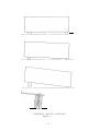
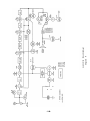
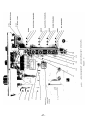
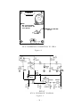
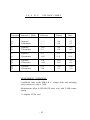
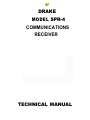
DRAKE
MODEL SPR-4
COMMUNICATIONS
RECEIVER
TECHNICAL MANUAL
Table of Contents
1.
1.1
1.2
GENERAL DESCRIPTION
Features
Specifications
1
1
2.
2.1
2.2
2.3
2.4
2.5
2.6
2.7
2.8
INSTALLATION
Unpacking
Location
Power Requirements
Antennas
Speakers
Headphone Operation
Viewing Angle Options
Rear Controls & Connectors
5
5
5
5
5
6
6
6
6
3.
3.1
3.2
3.3
11
OPERATION
11
Operating Controls
Simplified Operating Procedurel2
12
Dia1 Calibration
4.
4.1
4.2
4.3
4.4
4.5
4.6
4.7
4.8
4.9
4.10
PRINCIPLES OF OPERATION
Loop Amplifier
R .F . Amplifier
First Mixer
Premixer
Second Mixer
1 .F. System
Detection Systems
Audio Amplifier
AVC System
S-Meter
14
14
14
14
14
15
15
15
15
16
16
5.
5.1
5.2
5.3
ALIGNM ENT
Removing Cover
Trouble Shooting
Alignment Instructions
19
19
19.
19
6.
6.1
6.2
6.3
6.4
6.5
6.6
ACCESSORIES
SCC-4 Crystal Calibrator
S-NB Noise Blanker
RY-4 Radio Teletype Adaptor
TA-4 Transceive Adaptor
AVC Alterations
Service Data on Accessories
24
24
24
26
28
31
34
Fig. P a g e
Viewing Angle Options
1
4
Front Pane1 Operating Controls
2
9
Rear Controls & Connections
10
3
Block Diagram
4
13
Top Alignment Adjustment Points
17
5
Bottom Alignment Adjustment Points
18
6
SCC-4 Circuit Board
7
34
RY-4 Calibration Connection to SCC4 8
35
SCC-4 Schematic Diagram
9
35
S-NB Circuit Board
10
37
11
S-NB Schematic Diagram
38
RY-4 Circuit Board Installation
12
39
RY-4 Pictorial Wiring Diagram
13
39
14
RY-4 Circuit Board
40
41
RY-4 Schematic Diagram
15
TA-4 Circuit Board Installation
16
42
TA-4 Pictorial Wiring Diagram
17
42
TA-4 Circuit Board
18
44
19
TA-4 Schematic Diagram
45
20
Bottom View - Circuit Board
46
21
49
Transistor Lead Configuration
22
Loop Amplifier Circuit Board
50
RF Amplifier Circuit Board
51
23
Range Crystal Oscillator CircuitBoard24
52
Accessory Crystal Circuit Board
25
53
26
54
Premixer Circuit Board
27
55
Premixer Output Circuit Board
28
1st Mixer Circuit Board
56
29
2nd Mixer Circuit Board
57
58
1st IF Amplifier Circuit Board
30
31
58
2nd IF Amplifier Circuit Board
59
S -Meter Circuit Board
32
59
33
Notch Filter Circuit Board
60
34
50 kHz Filter Circuit Board
60
35
BF0 Circuit Board
61
36
AM Detector Circuit Board
61
37
Audio Amplifier Circuit Board
62
38
Power Supply Circuit Board
Accessory Crystal Chart
S C C - 4 DC/RF Voltage Chart
S-NB DC/RF Voltage Chart
RY-4 DC Voltage Chart
TA-4 DC Voltage Chart
SPR-4 DC Voltage Chart
SPR-4 RF Voltage Chart
SPR-4 Schematic Diagram
-33
-34
-36
-40
-43
-47
-48
Fold Out
1.
1.1
GENERAL
DESCRIPTION
FEATURES
The SPR-4 is an a11 solid-state communications receiver which can te
programmed with accessory crystals to cover 150 kHz to 30 MHz. The
SPR-4 receives AM, CW, SSB (Upper and lower ) and may be powered
from 120 VAC, 240 VAC and 12 VDC.
1.2
SPECIFICATIONS
1.2.1
GENERAL SPECIFICATIONS
Frequency Coverage : Can be programmed with accessory crystals for 23
ranges (each tuning a 500 kHz band ) from .5 to 30 MHz plus 150 to 500
kHz. Generous PTO dial overtravel allows additional 50 kHz or more off
each end of range. Crystals supplied with the receiver allow coverage
on these ranges ;
150
.5
1.0
6.0
7.0
-
500 kHz
l.0MHz
1.5 MHz
6.5 MHz
7.5 MHz
Modes of Operation:
Selectivity: AM
SSB
CW
RTTY
9.5 - 10.0 MHz
11.5 - 12.0 MHz
1 5 . 0 - 15.5 MHz
17.5 - 18.0 MHz
2 1 . 5 - 22.0 MHz
AM, CW, SSB (Upper and lower
RTTY adapter.
),
and RTTY with
4_8kHz@6dB, l0.0kHz@60dB
2 . 4 kHz@ 6 dB, 7.2 kHz @ 60 dB
.4
4 kHz @ 6 dB, 2.7kHz@ 60dB
With RTTY adapter, RTTY can be received in SSB
( lower ) or CW .
Sensitivity: SSB , CW, and RTTY: .2 5 microvolt for 10 dB S + N / N .
AM : .5 microvolt with 30% modulation for 10 dB S + N / N .
Intermediate Frequencies :
1st IF 5645 kHz, 2nd IF 50 kHz.
Frequency Stability: At room temperature, drift for a11 causes (including
+ 10% change in supply voltage) is les s than +- 100 Hz.
Automatic Volume Control: AVC is used on a11 modes. Time constants
are selected for the optimum effectiveness on each mode. Audio output
is held constant to 6 dB over a 100 dB range of input signals.
Input Impedance: 50 ohms approximately , on ranges C - H. On ranges
A and B, input is high impedance and plug in loop antenna is low impedance.
Audio Output Power: 3 watts into 4 ohm load (less into higher impedance loads ) .
Hum and Noise:
More than 60 dB below rated output.
Calibration: Dial is accurate to better than _+ 1 kHz when calibrated to
nearest 100 kHz calibration point.
1.2.2
POWER CONSUMPTION: 18 watts on 120 V DC, or 240 V AC, and 6 watts
2.5 watts on 12 V DC with dia1 lamps turned off.
on 12VDC.
1.2.3
SIZE AND WEIGHT:
1.2.4
SEMICONDUCTOR COMPLIMENT:
5-1/2” H x l0-3/4” W x 12-1/4” D ,
18 pounds .
Symbol
Type
Function
Ql
Q2
Q3
Q4
Q5
Q6
Q7
Q8
Q9
2N3394
2N3394
Loop Amplifier
Range Crystal OscilIator
PT0 B u f f e r
RF Amplifier
Premixer
PT0 Oscillator
1st Mixer
1st Mixer
D . C . Regulator
2nd Mixer
Crystal Oscillator
Audio Amplifier
Audio Amplifier
S-meter Amplifier
Audio Amplifier
Audio Amplifier
Crystal Oscillator Buffer
AVC Amplifier
Audio Amplifier
Audio Amplifier
Negative Supply Driver
Audio Amplifier
IF Amplifier
IF Amplifier
AVC Detector
Mute Control
BF0
AM Detector
Q10
Q11
Q12
Q13
Q14
Q15
Q16
Q17
Q18
Q19
Q20
Q21
Q22
Q23
Q24
Q25
Q26
Q27
Q28
2N3563
SFC4982, MFE3007
SFC4982, MFE3007
2N5950.
2N5245
2N5245
B5030
SFC4982, MFE3007
2N5245
B5030
B5030
2N5949, MPF102
2N3394
2N4125
2N5950, MPF102
2N4 125
2N3394
2N3394
2N3566
2N3394
SFC4982, MFE3007
SFC4982, MFE3007
2N3.566
2N4125
2N3394
2N3394
IC-1
CA3053
S-meter Amplifier
-2-
Symbol
CRl
CR2
CR3
CR4
CRS
CR6
CR7
CR8
CR9
CRl0
CRll
CR12
CR13
CR14
CR15
CR16
CR17
CR18
CR19
CR20
CR21
Function
Premixer Switch
RF Amplifier Protection
RF Amplifier Protection
Zener Regulator
Power Supply Rectifier
Power Supply Rectifier
Power Supply Rectifier
Zener Regulator
Zener Regulator
AVC Switch
AVC Switch
Negative Supply Rectifier
Negative Supply Rectifier
Zener Regulator
AVC Switch
AVC Switch
AVC Switch
AVC Switch
Product Detector
Product Detector
AM Detector
Type
lN270
lN4148
lN4148
lN714
B5G5
B5G5
B5G5
Z13B
lN714
lN4148
lN270
lN4148
lN4148
lN751
lN4148
lN4148
lN4148
lN4148
lN270
lN270
lN270
-
3
-
-
VIEWING ANGLE OPTIONS
Figure 1.
-
4
-
2.
2.1
INSTALLATION
UNPACKING
Carefully remove the receiver from the shipping carton, and examine it
for evidence of damage. If any damage is discovered, immediately notify the transportation company that delivered the receiver. Be sure to
keep the shipping carton and packing material, as the transportation company will want to examine them if there is a damage claim. Keeping the
carton and packing material is recommended even when no shipping damage occurs , as having the original carton available makes shipment of
the receiver much easier should it ever be necessary to return it to the
factory for service.
2.2
LOCATION
The SPR-4 will work well in almost any location. Extremely hot areas
such as over a radiator should be avoided. No air circulation around the
receiver is required .
2.3
POWER REQUIREMENTS
The SPR-4 will operate on 120 or 240 VAC 50/60 Hz or from any 12 15 VDC source with negative ground .
The SPR-4 is shipped from the factory ready for 120 V AC operation with
the power cord supplied. A 1/4 amp, slow-blow fuse, Buss type MDL
1/4, is installed in the fuse holder on the rear of the chassis .
For operating from 240 V AC , the same power cord is used and the 120 /
240 volt slide switch at the chassis rear is moved to the 240 position.
This requires moving the small metal keeper from the right to the left
mounting screw on the slide switch .
Also for 240 volt operation , the fuse should be
slow-blow, Buss type MDL 1/8.
changed to a 1/8 amp,
W A R N I N G : NEVER C O N N E C T T H E S P R - 4 T O 2 4 0 V O L T S
WITH THE SWITCH IN THE 120 VOLT POSITION.
For DC operation, a separate power cord is a11 that is required. This cord
is available with a cigar lighter plug installed.
2.4
ANTENNAS
For optimum performance the SPR-4 should be used with a good antenna.
For general broadcast and short wave listening, a long wire antenna from
-
5
-
50 to 100 feet long will give good results . An antenna kit (Mode1 AN-S)
is available.
For best single band performance, a half wave dipole or other resonant
antenna , fed with unbalanced 50 ohm coaxial table, may be used . How-
ever, Bands A and B require a long wire antenna.
For directional reception on 150 kHz to 1600 kHz, the accessory AL-4
shielded loop antenna may be used. All antennas other than the AL-4
loop antenna, connect to the Ant. jack on the rear of the chassis.
2.5
SPEAKERS
The SPR-4 has a built in 3” x 5” ceramic magnet speaker which makes optimum use of the available space in the cabinet. It may be desirable to
use an external speaker when the receiver is used at fixed locations .
The Drake MS-4 Speaker, housed in a cabinet that matches the SPR-4,
provides excellent audio reproduction and cornes equipped with a table
terminated in a phono plug matching the speaker socket on the rear of the
SPR-4.
2.6
HEADPHONE OPERATION
Best results will be obtained with a set of good quality headphones . T h e
headphone connection is made through the jack at the bottom left of the
front pane1 of the SPR-4. A standard 1/4 inch phone plug will mate with
the jack. Connecting the headphones to the receiver turns off the speake r . The SPR-4 will accommodate headphones of any impedance.
2.7
VIEWING ANGLE OPTIONS
As supplied, the SPR-4 sits with its base parallel to the mounting surface
and its front pane1 vertical to the mounting surface. With the studs and
rubber feet supplied, it is possible to position the SPR-4 for either of
two alternate viewing angles as shown in Figure 1. TO convert the SPR-4
to either option, remove the bottom row of three screws on each side ‘of
the receiver, and remove the bottom cover . For Option 1, remove the
rear feet and snap the small rubber feet into the holes just inboard from
the original rear feet and replace the bottom cover. For Option 2, remove
the front feet, invert them , and remount them with the same screws .
Thread one of the accessory studs into each of the remounted front feet.
Remove the rear feet and screw them onto the studs on the front feet and
replace the bottom cover.
2.8
REAR CONTROLS AND CONNECTORS
Refer to Figure 3 for the location of the connectors and controls .
-
6
-
2.8.1 P O W E R
The power connector mates with both the AC and DC power cords .
See “2 . 3 ”
2.8.2 FUSE
The fuse holder must have the proper fuse installed for 120 or 240 V AC
operation . See “2 .3 ”
2.8.3 SPEAKER
The interna1 speaker is normally connected to the speaker jack, when an
external speaker is used, disconnect the interna1 speaker by removing
the plug and connect the external speaker to this jack.
2.8.4 ANTI VOX and INJECTION
The holes marked ANTI VOX and INJ are intended for installation of
connectors for the TA-4 accessory which permits the SPR-4 to transceive
with the T-4XB. The injection and anti-vox tables from the T-4XB are
plugged into these jacks .
2.8.5 MUTE
A shorted phono connector is normally installed in the MUTE jack. When
the shorted connector is removed, the SPR-4 will be muted . When the
SPR-4 is used as a companion to the T-4XB, the mute table from the
T-4XB is plugged into this jack.
2.8.6 GROUND POST
A binding post is provided to allow connecting the SPR-4 chassis to
earth ground .
2.8.7 RTTY
The hole marked RY is intended for the installation of a connector for the
RY-4 accessory which permits the SPR-4 to receive RTTY signals . An external switch is plugged into this jack which enables RTTY reception
when the jack is shorted and the SPR-4 mode switch is in the CW or LSB
position .
2.8.8 AUDIO IN/OUT
The AUDIO IN/OUT jack provides approximately .08 volts of audio into
a high impedance load such as a tape recorder. The output level is independent of the setting of the AUDIO GAIN control.
-
7
--
The SPR-4 audio amplifier may be used with an external audio source
such as a tuner. The level of the external source must be approximately
.08 volts into a 3 K load . The received signals may be eliminated by
turning the RF GAIN control counter-clockwise or by removing the mute
plug
l
2.8.9 DIAL LAMPS
The DIAL LAMPS switch may be used to tum off the three dial lamps .
Since the power required to operate the dial lamps is somewhat greater
than the power required by the rest of the SPR-4, the operating time for a
battery power supply may be extended by turning the lamps off. The on
and off positions of the switch are interchanged when operating with a
DC power cord .
2.8.10 ANTENNA JACK
The antenna jacks mate with a standard phono fitting. A special antenna
fitting (a pin with a spring clip attached ) is supplied with the SPR-4 and
may be used by inserting it into the antenna jack. The antenna lead -in
is then connected to the clip.
2.8.11 ACCESSORY CRYSTAL INSTALLATION
The top of the SPR-4 cabinet must be removed in order to install additiona l crystals . This is accomplished by removing the top row of screws on
both sides of the set. Also, disconnect the table from the speaker jack.
Be sure the power tord is disconnected. The top of the cabinet may now
be removed .
At the bottom of each segment of the crystal selector dial is a small num-.
ber (0 - 23 ) which corresponds to a particular crystal socket . The crystal location diagram which is located on the chassis behind the crystal
sockets indicates the number of each socket. No crystal is required for
reception of 15 0 - 500 kHz, therefore there is no crystal socket numbered
zero .
Install the accessory crystal in one of the empty sockets . Locate the
appropriate crystal dial decal from the sheet supplied with the crystal.
Remove the decal from the sheet by cutting along the appropriate lines
with a pair of scissors . Remove the backing from the decal and install it
in the dial sector with the same number as the crystal socket used. Replace the cabinet top and the speaker table.
On certain ranges there are spurious interna1 signals which are unavoidable in this double conversion, super-heterodyne receiver. These are
due to outputs of interna1 conversion oscillators. There are five frequencies that should be avoided if possible. These are; 5.222 MHz, 5.595
MHz, 5.695 MHz, 9.963 MHz, and 15.334 MHz.
-
8
-
a,
3.
OPERATION
Refer to Figure 3 for the location of the operating controls.
3.1
OPERATING CONTROLS
1.
The S-meter indicates the relative level of the received signals .
2.
The crystal selector switch selects the band determining crystals .
The top line of the dial sector reads the lowest frequency of each
band in MHz, the middle line indicates the approximate position for
tuning the preselector and the bottom line indicates the proper setting of the range switch.
3.
The main tuning dial reads 0 to 500 kHz with 1 kHz graduations.
When the tuning dial reading is added to the crystal dial reading ,
the actual received frequency is indicated to 1 kHz.
The
that
disc
may
main tuning dial consists of two concentric transparent discs
rotate at different speeds . Zero to 100 kHz is indicated on one
and hundreds of kHz are indicated on the other disc. The dial
be calibrated by rotating the skirt with respect to the knob.
4.
The preselector is set to the position indicated by the number on the
middle line of the crystal selector dial and then fine tuned for peak
signal .
5.
The range switch sets up the proper tuned circuits to cover the desired band of frequencies . It is set to the position indicated on the
bottom line of the crystal selector dial.
6.
The headphone jack mates with a standard 1/4 inch phone plug. Connecting the headphones to the receiver will turn off the speaker.
7.
The audio gain control adjusts the audio output to the proper level.
8.
The RF gain control controls the gain of the receiver for a l l signals
which are below the AVC threshold level to which the control is set.
This control is normally set in the full clockwise position. Counterclockwise rotation reduces the gain of the receiver.
9.
The mode selector switches in a product detector for CW and SSB or
a diode detector for AM. The proper I. F. bandwidth and AVC time
constant is also selected.
10.
The notch control may be used to eliminate or reduce an interfering
heterodyne or CW signal. The off position, which is shown in
Figure 2, has a positive detent. Counter-clockwise rotation of the
-
ll-
knob from the off position moves the rejection notch across the receiver pass band .
11.
3.2
The accessory switch turns on the S-NB Noise Blanker and the SCC-4
Crystal Calibrator if they are installed. The 5-NB and the SCC-4 are
off in the NORM position.
SIMPLIFIED OPERATING PROCEDURE
As an example , suppose that the SPR-4 is to be tuned to 7272 kHz. First
turn the crystal selector dial to the 7.0 MHz position. Set the preselector to 5.5 as indicated on the second line of the crystal selector dial .
Next set the range switch to E as indicated on the bottom line of the
crystal selector dial. Turn the tuning knob until the 100 kHz dial is between 2 00 and 300 and the one kHz dial is on 72. Select the desired
mode of reception with the mode switch. The RF gain control should be
full clockwise and the notch should be in the off position. Turn on the
receiver with the audio gain control and adjust it for normal audio output.
Fine tune the preselector for maximum indication of the S-meter.
The frequency of the received signal is the sum of thè crystal dial reading and the main tuning dial reading as shown by the example:
3.3
Crys ta1 Selector Reading
100 kHz Dial Reading
1 kHz Dial Reading
7 .000 MHz
.200
Frequency of Received Signal
7.272 MHz
.072
DIRL CALIBRATION
The main tuning dial calibration may be adjusted over a short frequency
range by using the known frequency of the SCC-4 crystal calibrator or a
station such as the National Bureau of Standards , WWV, on 2.5, 5, 10,
15, 20, and 25 MHz. Usually 5 and 10 MHz WWV signals are the easiest to receive . With the mode switch in the CW, LSB or USB position,
tune the signal from the SCC-4 or WWV to zero beat. Hold the main
tuning knob stationary and rotate the skirt until the dial reads the correct
frequency .
-
12-
.;
-13-
4.
4.1
PRINCIPLES OF OPERATION
LOOP AM PLIFIER
On Bands A and B , Q1 amplifies signals from the loop antenna and feeds
one gate of the R.F. amplifier Q4, through C52 and the tuned circuits
formed by C9, Cl0, C13, C16, C18, C22, C23, C25, C27, C33, T2,
and T4.
On Bands A and B, signals from an external antenna connected to J2 (AA)
bypass Q1 through Cl0 and Cl3 into the tuned circuits described above.
4.2
R.F. AMPLIFIER
On Bands C through H signals from an external antenna connected to J2
(ANT ) are coupled to Q4 through T3 and C52..T3 is resonated with C101
and the capacitors connected to S5R. Q4 is protected from large signals
by CR2 and CR3 which are reverse biased. CR2 and CR3 limit the signal
to a safe level by conducting when a large signal overcomes their reverse
bias .
On Bands A and B the drain of Q4 is untuned and drivès the 1st mixer
through C90 and C96. On Bands C through H , the drain of Q4 is tuned by
T5, the capacitors connected to S9F, and drives the 1st mixer through
C90.
4.3
FIRST MIXER
The 1st mixer is a balanced mixer comprised of Q7 and Q8 and driven by
the R .F . amplifier and the pre-mixer . On Band A, the pre-mixer is bypassed and the 1st mixer is driven from the P.T.O. through R25 and C99.
On Bands B through H, the pre-mixer drives the 1st mixer through T6 and
C99.
The 1st mixer is balanced by R40 and the output is tuned by Cl02 and T8
and drives the 2nd mixer through C110, the 5645 crystal filter, and T9.
Heterodyning of the R.F. amplifier and pre-mixer (P.T.O. on Band A)
results in a difference frequency output from Q7/Q8 of 5645 kHz.
4.4
PREMIXER
The premixer system consists of the P .T .O. , the crystal oscillator Q2,
the premixer transistor QS, and the tuned circuits associated with S1,
S4F, S4R, S8F, a n d S8R.
The collector of the crystal oscillator Q2 is tuned by L5 and the components connected to S1.The feedback winding on L5 is connected
through S2 to the proper range ctystal and the output of Q2 is connected
- 1 4 -
-
to one gate of the premixer, Q5 through C26 and R15. The P.T.O. drives
the other gate of Q5 through R25 and C76. The P.T .O. is tuneable from
4955 kHz to 5455 kHz.
The output of Q5 is tuned by the components associated with S4F, S4R,
S8F, S8R and drives the 1st mixer through T6, S6R, C99 and C96.
4.5
SECOND MIXER
The 2nd mixer, Q10, is driven by the 1st mixer and the crystal oscillator
buffer Q17. Q10 is coupled to the 1st IF amplifier through the T notch
filter and the 50 kHz four pole Hi-Q ferrite L C filter. Heterodyning of
the 1st mixer and crystal oscillator results in a difference frequency output from Q10 of 50 kHz.
4.6
1. F. SYSTEM
The I .F . system is composed of the 1st I .F . amplifier, 423, which drives
through T 15, the 2nd I. F. amplifier, Q24. C169 and C187 tune T15 and
T16 respectively to 50 kHz and T16 drives the detection systems .
4.7
DETECTION SYSTEMS
4.7.1 AM DETECTION
The AM signal from T16 is detected by CR2 1 and amplified by Q28 to a
level matching the output level of the product detector and is applied to
the audio gain control through C 167 and S 14F.
4.7.2 CW AND SSB DETECTION
CW and SSB signals from T16 are detected by the product detector made
up of CR19, CR20, R122, R123, and Q27, the beat frequency oscillator.
The output of the product detector is applied to the audio gain control
through S 14F.
4.8
AUDIO AM PLIFIER
A portion of the audio signal, determined by the setting of Rl0l , is applied to Q22 through a low-pass filter consisting of L10, L11, C164,
R97, R95, C 163, and C159 which eliminates any residual 50 kHz signal
from driving the audio amplifier. Q22 amplifies this audio signal and
drives Q20 through C 148 where further amplification occurs and Q2 0
drives Ql6 directly and Q15 via Q19 which is unity gain common base
amplifier. Q12, Q 15 and Q13, Q16 are darlington connected amplifiers
and the configuration of Q16 establishes a phase inversion permitting
Q12 and Q13 to operate in push-pull, Q12 and Q13 operate the speaker
or a headphone through coupling capacitor C 127.
-
15
--
4.9
AVC SYSTEM
The AVC threshold is established by the setting of R111, the R.F. gain
control. R111 is normally operated fully clockwise . This applies approximately +2 volts to the AVC line through R104, R100 and CR15 with no
received signal. Signals from T16 drive Q25 into base current on the positive R .F . driving cycle which pulls the collector negative because the
emitter is returned to the - 5 volt line. The negative potential on the collector of Q25 is applied to the AVC line through CR18 and to C 171
through CR17. The rate that C162 is charged determines the AVC attack
time. The AVC release time is determined by the rate that C 171 discharges through R100 allowing Cl62 to discharge through CR15. The attack and release times for Q4 are lengthened by R22 and C70 to eliminate
undesirable transients.
Large signals are kept from overloading Q4 by the application of a positive voltage on Pin 3, the signal gate. This voltage is derived from the
S-meter and Q-18 and the delaying circuit of CR10, R47, R52, and C180.
On AM , S 14R shorts out CR10 to obtain a symmetrical attack and release
response.
4.9.1 MUTING
Muting is accomplished by placing an open circuit at J9 which removes
base current from Q26, lowering its collector voltage to -5 volts. The
cathode of CR16 will also be at -5 volts causing it to conduct, applying
cut-off voltage on the AVC line which turns off Q4, Q10, Q23, and Q24
and mutes the receiver.
4.10
S -METER
The S-meter is a voltmeter that measures the AVC voltage and is calibrated in ” S ” units . The source follower Q14, is connected to the AVC line
and drives IC- 1 which is a differential amplifier that operates the Smeter. The zero adjustment is affected by R64 and the S-meter full scale
sensitivity is set by R73.
-
16
--
-17-
-18-
5.
5.1
ALIGNMENT
REMOVING COVERS
Remove the AL-4 Loop Antenna if it is in use. Remove the top three screws
on each side of the SPR-4 and remove the top cover by pulling up on the
rear and then on the front of the cabinet. Remove the remaining screws
from the bottom cover and lift the SPR-4 from out of the bottom cover.
5.2
TROUBLE SHOOTING
Careful consideration has been given in the design of the SPR-4 to keeping maintenance problems to a m i n i m u m . If you experience difficulty we
recommend that you return the unit to your Drake dealer or write direct to
our Customer Service Department describing your problem in detail. Include full information concerning external connections, control settings ,
antenna used , serial number, etcetera.
D O N O T R E T U R N E Q U I P M E N T T O T H E F A C T O R Y WITHOUT P R I O R A U T H O R I Z A T I O N !
The voltage and parts location charts which follow should be
valuable in isolating service problems . However, no attempt should be
made to service the SPR-4 unless you are thoroughly familiar with electronic circuitxy and transistor and printed circuit servicing technique.
C A R E S H O U L D B E T A K E N N O T T O D I S T U R B T H E LEAD
DRESS IN THE SPR-4 SINCE THIS. IS CRITICAL IN
SEVERAL CIRCUITS.
5.3
ALIGNMENT INSTRUCTIONS
Alignment of the SPR-4 requires the use of the following equipment.
1.
A stable R.F . signal generator with variable output that can be accurately set to any frequency in the range from 50 kHz to 3 0 MHz .
2.
A voltmeter having an input impedance of 11 Megohms or greater,
such as a VTVM.
3.
The following accessory crystals :
40.59
39.59
25.09
14.59
12.59
MHz
MHz
MHz
MHz
MHz
for 2 9 . 5
for 28.5
for 14.0
for 3 . 5
for 1.5
- 30.0
- 29.0
- 14.5
- 4.0
- 2.0
-
MHz
MHz
MHz
MHz
MHz
19
reception
reception
reception
reception
reception
---
5.3.1
5.3.2
4.
An accessory crystal for reception of WWV standard frequency transmission that is most reliably received in your area.
See Page 33 to determine crystal frequency required. This
crystal is not required if SPR-4 does not have an SCC-4 Crystal Calibra tor .
5.
A 47 ohm 1/2 watt composition resistor connected across a phono plug
to serve as an antenna load.
6.
A scale with accurate 1/32 inch divisions.
7.
An alignment tuning wand such as General Cernent GC 8273 or
Walsco 25 16.
50 kHz I.F., B.F.O., and 50 kHz LC Filter Alignment
1.
The settings of the range, preselector, crystal selector, and PT0 controls are unimportant for this portion of the alignment . Set the audio
gain at 12 o’clock, the RF gain fully clockwise, mode switch to LSB ,
notch to OFF, and accessory switch to NORM.
2.
Connect a VTVM to the AVC line . This line is accessible at the terminal on the 1st I. F. board with the two white/green tracer wires attached .
3.
Connect a 50.0 kHz unmodulated signal generator to Gate 1 (pin 3)
of Q10 which is the terminal on T9, right side and closest to the
front pane1 when looking into the bottom of the SPR-4 and front
pane1 facing you.
4.
Set the generator level SO that slight AVC deflection (negative
going) can be observed and adjust T17 for zero beat.
5.
Adjust T-15 and then T16 for maximum deflection of AVC voltage.
6.
Set the signal generator to precisely 50.8 kHz and put the mode
switch on CW and tune L11, L12, L13, and L14 for maximum AVC
deflection.Repeat tuning L11 through L14 until no further improvement can be obtained.
5645 kHz I. F. Alignment
1.
With the receiver set up as in 5.3.1, connect the signal generator
to the junction of R27 and C90. This point is accessible at the ter-
-20-
-
minal on the R.F. amplifier board at the left top corner, looking into
the bottom of the SPR-4 and front pane1 facing you. This terminal
has coax connected to it . Care should be taken not to short this
point to ground because Q4 will be ruined,
2.
Preset the balance pot on the 1st mixer board fully clockwise.
3.
Set the signal generator to 5645 kHz and adjust its level for a slight
AVC deflection.
4.
Place the mode switch in LSB and adjust C 115, the outer trimmer
capacitor on the mixer oscillator board for zero beat .
5.
Place the mode switch in USB and adjust C 113, the inner trimmer
capacitor on the mixer oscillator board for zero beat.
6.
Set the signal generator to 5650 kHz, the mode switch to LSB and
adjust T8 and then T9 for maximum AVC.
7.
Set the generator to 5645 kHz and adjust the mixer balance pot for
minimum AVC deflection (most positive going ).
PRESELECTOR AND INJECTION ALIGNMENT
1.
The settings of’the range,preselector, crystal selector, and PTO will
be indicated before each adjustment. Set the audio gain at 12
o’clock, the RF gain fully clockwise, mode switch to LSB, notch to
OFF, and accessory switch to NORM .
2.
Install the accessory crystals listed at 5.3.3 on Page 19. Plug the
47 ohm resistor into the antenna jack, J2.
3.
Tum the preselector control fully clockwise and check the shield
cans marked Tl , T2, T3, T4, T5, and T6 for proper slug engagement.
The distance from the top of the slugs to the top of the white coil
forms should be 9/16” . T2 and T4 may differ from this figure by 1/32”
on receivers from the factory. These s lugs may be left alone for
“Touch up” alignment . For complete alignment, set a l l slugs to
9/16”.. Turn the preselector control fully counterclockwise and set
the pointer on zero.
4.
Tune in the calibrator signal or an unmodulated signal generator
loosely coupled to the 47 ohm antenna load at 30.0 MHz (range
switch on H with 40.5 9 MHz crystal, dial on 500. ) Rough tune a l l
H band trimmers for maximum S-meter reading and/or maximum AVC
deflection.
5.
Tune in the calibrator or a signal generator at 28.7 MHz and repeak
the preselector for maximum AVC deflection . Tune the H band R .F .
-21-
and mixer trimmers for maximum AVC deflection. Detune T6 by grasping a metal screwdriver shaft and touching it to the rotor contact of
S4R, and tune the rear H band injection trimmer for maximum AVC
deflection. Detune T1 by touching the rotor contact of S8F and tune
the front H band injection trimmer for maximum AVC deflection.
6.
Tune the G through C bands with the following set-up, tuning the R.F.
and mixer trimmers first, followed by the injection trimmers taking
care to use the loading techniques described in 5 (above ) . The
identification and location of the trimmers can be found in Figure
and Figure
Calibrator or Signal Generator
BAND Frequency in MHz.
7.
G
F
E
D
21.5
14.0
6.0
3.8
C
1.9
Preselector Setting
9.0
7.5
4.0
R.F. slug tops flush with
white coil form
R.F. slug tops flush with
white coil form
BANDS A and B ALIGNMENT
Remove the 47 ohm antenna load and tune in the calibrator or a signal
generator at 300 kHz on Band A and set’the preselector to exactly 6
on its scale. If a signal generator is used, a 10 pf coupling capacitor
should connect the generator to the antenna jack. Adjust the slugs of
shield cans T2 and T4 for maximum AVC deflection.
On Band B tune in the calibrator or signal generator at 1600 kHz and
tum the preselector control fully clockwise and rough tune a l l B band
trimmers for maximum AVC deflection. Retune to 1400 kHz and carefully peak the signal with the preselector control. Tune the B band
R . F . , mixer, and injection trimmers ( properly loaded ) for maximum
AVC deflection. The accessory crystals used especially for alignment may now be removed.
5.3.4
NOTCH FILTER ALIGNMENT
Tune in the calibrator or signal generator on LSB for a zero beat and set
the notch knob to, 3 o’clock. The notch slug should be as far into the
coi1 as it will go without engaging the stop. If it isn’t , rotate the notch
knob to its OFF detent , loosen the notch knob setscrew and tighten it in
the OFF position. Return the knob to the 3 o’clock position and adjust the
notch slug for maximum AVC voltage (positive going) . Switch to AM, set
- 2 2 - -
the notch control at 12 o’clock and adjust the main tuning knob for maximum AVC voltage ( positive going ) . Altemately adjust the notch control
and the notch depth control, R57, for maximum AVC voltage (positive
going ) .
5.3.5 S-METER ADJUSTMENT
Tune in a 10,000 microvolt signal on 7.2 MHz LSB and looking into the
top of the chassis with the front panel facing you, adjust R73, the left
control on the S-meter circuit board for + 4.5 volts on the middle top terminal of the meter board and has a white/black tracer wire connected to
it . Remove the 10,000 microvolt signal and adjust R64, the right control
for meter zero . Because these controls interact slightly, repeat the above
procedure until no further interaction occurs .
-
23
-
6.
ACCESSORIES
6.1
MCDEL SCC-4 CRYSTAL CALIBPATOR
6.1.1
GENERAL DESCRIPTION
6.1.2
6.1.3
The SCC-4 is a 100 kHz crystal controlled oscillator that injects into the
receiver a harmonic every 100 kHz throughout the SPR-4 frequency coverage .
INSTALLATION
Remove the top row of 3 screws on each side of the SPR-4 cabinet. Disconnect the power cord, internal speaker cable and remove cabinet top.
Install the SCC-4 by inserting it into the socket marked CALIBRATOR at
the left rear of the SPR-4 chassis. Replace the cabinet top, power cord,
and speaker cable.
OPERATION
The calibrator is switched on by placing the accessories switch on the
front panel in the CAL position.
6.1.4
CIRCUIT DESCRIPTION
Transistor Q2 and the 100 kHz crystal form the oscillator which drives the
harmonic amplifier Q1. Harmonics of 100 kHz are generated by the wave
shaping diode CRl.’ The amplified 100 kHz harmonics are coupled to the
SPR-4 antenna input through C2.
6.1.5
SERVICE DATA
A voltage chart ,schematic and a circuit board layout, Figure 7
provided for servicing the SCC-4.
are
6 . 1 . 6 ALIGNMENT
The SCC-4 is factory aligned, but due to shock and vibration during
shipment, or normal long term drift, adjustment is sometimes necessary .
Tum on the receiver and the calibrator and allow it to warm up for at
least 30 minutes . Tune in a standard frequency station such as WWV
Carefully adjust the ceramic trimmer capacitor located on top of the calibrator circuit board for zero beat . This completes a l l necessary alignment.
6.2
MODEL 5-NB NOISE BLANKER
6.2.1
GENERAL DESCRIPTION
The 5-NB is a solid state noise blanker for use with the SPR-4 Receiver.
The 5-NB works by muting the receiver for the duration of the noise
-
24
--
puls e. Between noise pulses , full receiver gain is restored . Receiver
AVC is affected only by the desired signal and not by noise when the
5-NB is in use. The 5-NB is most effective on strong, periodic impulse
noise such as ignition noise.
6.2.2 INSTALLATION
T O install the 5-NB, remove the top row of three screws on each side of
the SPR-4 Receiver cabinet. Disconnect the power cord, the internal
speaker cable and remove the cabinet top. Unplug the jumper cable from
the two sockets near the power transformer and marked noise blanker .Retain the jumper cable SO that it may be used if the S-NB should ever
require service. Install the 5-NB by plugging it into the two sockets on
top of the SPR-4 chassis.. Be sure that the 5-NB is seated in the sockets
and do not disturb any components on the 5-NB circuit board. Replace
the cabinet top, power cord , and speaker cable .
6.2.3 OPERATION
The 5-NB is controlled by the SPR-4 accessory switch. When the accessory switch is in NB position, the 5-NB is turned on. The accessory
switch may be left in the NB position for full time protection against
noise interference . Some distortion may be noted when using the 5-NB on
extremely strong signals .
6.2.4 CIRCUIT DESCRIPTION
Signals at the I .F . frequency from the 1st mixer in the SPR-4 pass
through the two pole crystal filter in the 5-NB and are amplified by Q4.
The signal on the collector of Q4 is coupled to Q9 and Q 10 through T2 ,
C27, T3 and C33 where it is amplified further and passes through T4 to
the series gate CRl , CR2 and into the SPR-4 I .F . through T5 . The I.F .
signal on the emitter of Q4 is coupled through C 16 to Ql which drives
the balanced mixer, Q5 and Q6. The balanced mixer subtracts the I. F .
signal from the crystal oscillator Q3 and the difference frequency is coupled to Q7 through T7 and C23. Transistors Q7 and Q8 amplify the mixer
output . The collector of Q8 drives the pulse detector, Q 15 and the AGC
amplifiers, Q l l , Q13 and Q14. Q14 drives Q2 and Q16 which control
the gain of Q1 and Q7 respectively . The AGC system maintains the amplitude of the signals at the collector of Q8 SO that the pulse detector,
Q15, remains tut-off for normal radio communication signals . When
transistor Q15 is cut-off, Q12 conducts and applies a positive potential
to the center tap of the secondary winding of T4 which is greater than the
+ 1 volt applied ,to the center tap of T5 primary maintaining the series
gate in the "on" state . With the series gate “on”, radio signals pass
through the 5-NB unaffected. Noise impulses larger than the average
communication signal will turn on Q15 for the duration of the impulse .
This turns off Q12 for the same duration causing the series gate to be
-25- -
reverse biased and turned “off”. With the series gate “off”, the signal
path through the 5-NB is broken and reception is blanked for the duration of the interferring noise pulse. The 5-NB is turned on by the accessory switch in the SPR-4 which removes the ground from Pin 1 of P-5 and
allows Q3 in the 5-NB to oscillate permitting signals to mix in the 5-NB
balanced mixer and eventually operates the series gate.
6.2.5 SERVICE DATA
A voltage char-t, s chematic , and a circuit board layout , Figure 10 are
provided for servicing the 5-NB.
6.2.6 ALIGNMENT
The 5-NB requires no alignment at the time of installation. However,
should alignment ever become necessary, the following procedure should
be used.
Connect a VTVM at 15 volts full scale between the chassis and R46 of
the 5 -NB (see Figure 10 ) . Tune the SPR-4 to 2 1.9 MHz while using a
signal generator as a signal source. With the 5-NB turned off, ad just
C-21, C-26, and C-28 for maximum S-meter reading. It may be necessary to touch up the adjustment of C-21 for the best AM passband as indicated by the S-meter. With the accessory switch in NB position, and
the signal source turned off, adjust R-19 for maximum positive voltage
on R-46. With the’signal source turned on, adjust C-7 and C-18 for
minimum voltage on R-46. Tune the SPR-4 to 2 1.5 MHz while using the
2 1.5 MHz crystal. With the signal generator turned off, adjust the
spacing between C12 and C49 for maximum voltage on R-46. With the
signal generator turned on, and still on 21.9 MHz, adjust R-38 so that
the S-meter has the same reading with the 5-NB installed as it does with
the jumper cable installed.
6.3
MODEL RY-4 RADIO TELETYPE ADAPTOR
6.3.1 GENERAL DESCRIPTION
The RY-4 Radio teletype Adaptor allows the 50 kHz BF0 in the SPR-4 to
be remotely switched so that standard shift RTTY tones may be center ed
in the passband of the 50 kHz I .F. filter. The switching is performed by
an external circuit which must short the RTTY jack to ground.
When the mode switch is in the CW position and the RTTY jack grounded,
the BF0 frequency will be switched to 48.590 kHz so that standard 2125
and 2295 Hz tones may be received.
When the mode switch is in the LSB position and the RTTY jack grounded,
the BF0 frequency will be shifted to 49.350 kHz so that standard 2 125
and 2975 Hz tones may be received.
-26--
When the mode switch is in the AM or USB position, shorting the RTTY
jack will have no effect.
6.3 .2
INSTALLATION
This modification should be made by a competent technician. If you need
help or want the RY-4 to be installed by one of our factory authorized
service centers or by the factory service technicians , please call or
write our Customer Service Department .
Disconnect the speaker cable, the line cord , and remove the SPR-4 cabinet. Mount the circuit board in the location shown in Figure 12 using
a No. 4 sheet metal screw with a No. 4 lockwasher between the screwhead and the mounting foot. Some early SPR-4 Receivers may not have
the hole in the chassis. In this case, mount the circuit board foot under
the No. 6 nut on the PTO spade bolt as shown in Figure 12 .
Mount the phono jack (with nut, lockwasher and ground lug on the inside
of the chassis) in the hole next to the grounding screw on the rear apron
of the chassis. Connect the .01 disc capacitor between the phono jack
and the ground lug. Solder only the ground lug. connect the 3 wires
between the terminals on the RY-4 circuit board and the terminals on the
BF0 board as shown in Figure 13. Use bare wire and sleeving .
D 0 N 0 T use any more heat than necessary when soldering the terminals as the circuit boards may be damaged.
Connect the 3 color coded wires between the RY-4 circuit board terminals
and switch S-14R as shown in Figure 13 . Connect the white/yellow
wire from the RY-4 circuit board to the installed phono connector. Dress
this wire along the wiring harness . Solder a l l connections.
The BF0 transformer T-17, must be adjusted for 50 kHz. Place the mode
switch in the USB position and the RF gain control fully clockwise. The
position of the crystal selector, range switch, and preselector is unimportant. Connect a clip lead with a series blocking capacitor of 1000 pf
between the terminal on T-15 and the 10 K resistor of the SCC-4 crystal
calibrator . See Figure 8
and Figure 12 . Adjust the slug in T-17 for
zero beat. Remove the clip lead and replace the cabinet, If an SCC-4 is
not available, follow the B.F.O. alignment in “5 -3.1” and make certain
the RTTY jack on the rear of the SPR-4 is not connected to ground.
6.3.3 OPERATION
Reception of standard shift (850 Hz) RTTY signals is accomplished by
placing the mode switch in
position and shorting the RTTY jack with
an external switch provided by the user. Reception of narrow shift
( 170 Hz ) RTTY signals is accomplished by placing the mode switch in CW
position and shorting the RTTY jack with an external switch.
-
27
--
6.3.4
CIRCUIT DESCRIPTION
The BF0 is shifted in frequency for RTTY reception by shunting a capacitor
across T17 with an electronic switch . Transistor Q2 electronically
switches C2 across T17, and Q3 switches C3. Switch S14R connects
the collector of Q1 to the base of Q3 in CW and to the base of Q2 in LSB .
If Jl (RTTY jack) is shorted, Q1 conducts and turns on either Q2 in LSB
or Q3 in CW, allowing reception of RTTY signals .
6.3.5
SERVICE DATA
A voltage chart ,schematic and a circuit board layout , Figure 14 are
provided for servicing the RY-4.
6.3.6
ALIGNMENT
Place the mode switch in t he USB position and the RF gain control fully
clockwise . The position of the crystal selector, range switch and pres elector is unimportant. Connect a clip lead with a series blocking
capacitor of 1000 pf between the terminal on T15 and the 10 K resistor of
the SCC-4 crystal calibrator. See Figure 8 and Figure 12 . Adjust
the slug in T- 17 for zero beat . Remove the clip lead and replace the
cabinet. If an SCC-4 is not available, follow the BF0 alignment in
“5.3.1” and make certain the RTTY jack on the rear of the SPR-4 is not
connected to ground .
6.4
MODEL TA-4 TRANSCEIVE ADAPTOR
6.4.1
GENERAL DESCRIPTION
The TA-4 Transceive Adaptor allows the SPR-4 to transceive with the T-4A
T-4B/T-4X/T-4XB Drake Transmitters .
6.4.2
INSTALLATION
This modification should be made by a competent technician . If you need
help or want the TA-4 to be installed by one of our factory authorized
service centers or by the factory service technicians, please call or
write our Customer Service Department.
Disconnect the speaker table and the line cord and remove the SPR-4
cabinet. Mount the TA-4 circuit board with two number 4 sheet metal
screws and two lockwashers (with the lockwashers between the screwheads and the mounting feet) in the chassis holes as shown in Figure 16 .
Connect the five color coded TA-4 circuit board wires by pushing the
connectors at the end of each wire onto the appropriate mating pins in the
SPR-4 until they are fully seated. See Figure 17 for the location of the
-
28--------------
Late SPR-4’s have a 12 K 1/2 watt resistor between T-6 and the preCut the resistor lead from T-6 and remove the resistor. Route
mixer board
the coax cable along the wiring harness and install the phono fitting on the
end of the cable in the large hole near the center of rear chassis apron a s
shown in Figure 17 . The nut and the flat washer should be on the outside
of the chassis .
pins .
.
Remove the SPR-4 S-meter lamp bracket by squeezing the sides of the
bracket. Remove the lamp bracket from the crystal selector frame by
removing the mounting screw.Locate the audio transformer mounting feet
over the two holes in the top of the chassis which are in front of the
crystal selector. The black transformer lead should be facing the front
Mount the audio transformer by inserting number six screws
panel
through the chassis holes from the bottom and into the speed nuts on the
transformer. Route the two transformer leads through the rectangular
chassis hole.. Push the pin on the black wire into the clip on the headphone jack. Some early SPR-4 Receivers do not have this clip. In this
case, solder the black wire to the headphone terminal closest to the RF
Route the red wire along the wiring harness to
and audio gain controls
the rear of the chassis and mount the phono fitting in the 3/8 inch hole
directly below the speaker jack.. Some early SPR-4 Receivers may have a
1/4 inch hole in this location. In this case, enlarge the 1/4 inch hole to
3/8 inch.. Replace both lamp brackets
.
.
.
It will be necessary to adjust the injection trimmers after the TA-4 installation . S e e “ 5 . 3 , Paragraph 3” for the required accessory crystals for
tuning the injection trimmers . Tune in the signals in the chart below
from a signal generator or the crystal calibrator and peak
the preselector for maximum S-meter reading. Detune T6 by grasping a
metal screwdriver shaft and touching it to the rotor contact of S4R and
tune the rear most injection trimmer for the band under alignment for maximum AVC deflection or S-meter reading . Detune T1 by touching the
rotor contact of S8F and tune the front injection trimmer for maximum AVC
deflection or S-meter reading.
BAND
FREQUENCY IN MHz
H
G
F
E
D
C
B
28.7
21.5
14 .o
6.0
3.8
1.9
1.6
MHz
6.4.3 OPERATION
The TA-4 is activated by circuits in the Drake T-4/T-4B/T-4X/T-4XB
Transmitters , therefore operation of the TA-4 is performed at the trans-
ceive switch on these transmitters .
-
29
-
6.4.4 CIRCUIT DESCRIPTION
The transceive switch on the T-4/T-4B/T-4X/T-4XB Transmitter controls
the TA-4 by applying a negative or positive D.C. potential to the injection c a b l e. When the transceive switch on the transmitter is in SPOT
position, no D.C . potential is applied to the injection cable and the
injection cable is not utilized . In SEPARATE position, the injection line
is connected to the mute jack through a 68 K resistor. The mute jack in
the SPR-4 becomes positive under open circuit (receiver muted) condition
which supplies base current through R6, CR2 and CR3 to Q2 and turns it
on. Whenever, Q2 is on, Q l , Q3 and Q4 are also conducting. The collector current in Q4 drops the gate voltage on the SPR-4 premixer transistor Q5 and cuts it off which éliminates the possibility of the SPR-4 injection frequency from getting into the transmitter and causing a spurious
signal.
In RCVR position, the cathode of the premixer tube, V8, in the T-4/T-4B/
T-4X/T-4XB Transmitter is connected directly to the injection line which
makes it positive, but not enough to cause CR2 to conduct preventing Q4
from disabling the SPR-4 premixer.
T-6 in the SPR-4, drives Q5, an emitter follower, through C5 and R-12 in
the TA-4. The output of Q5 drives the injection jack through C7 which
allows the T-4XB to transceive on the SPR-4 dial frequency.
In XMTR position, the injection line is made negative which turns on Q1,
Q3 and Q4. Collector current in Q4 drops the gate voltage on the SPR-4
premixer transistor Q5 and cuts it off. The injection frequency signal
from the transmitter drives the center tap on the link of T6 through Q1
which is used as a switching diode.
T1 in the TA-4 ,is an audio transformer which matches the SPR-4 audio output impedance to the anti-vox circuit in the transmitter.
6.4.5 SERVICE DATA
A voltage chart, schematic, and circuit board layout, Figure 18
provided for servicing the TA-4.
are
6.4.6 ALIGNMENT
The carrier oscillator in the T-4XB must be adjusted SO that the SPR-4
and the T-4XB will transceive. Both SPR-4 carrier oscillators must be
on frequency . The SPR-4 oscillators are set at the factory and should
not require any adjustment . If the SPR-4 alignment is under suspicion,
perform the 5 0 kHz IF and 5645 kHz IF alignment described in 5.3.l
and 5.3.2.
-
30
-
CONTROL OR SWITCH
S PR-4
Band or Range switch
Crys tal switch
Function
Mode
Audio Gain
Transceive
Anti -Vox
S ideband
D
3.5
--LSB
3 o’clock
-------
Preselector
Both the SPR-4 and T-4XB preselectors
should be set to about 6.5 and peaked
for the loudest “canary” sound from
the speaker.
T-4XB
3.5
--SSB
--_
--spot
Full clockwise
Lower
Adjust C-2 in the T-4XB until the “canary” sound slows down to only a
few chirps a second and then zero chirp a second and a l l that is heard is
a single tone.
6.5
AVC ALTERATIONS
6.5.1 GENERAL DESCRIPTION:
It is possible to alter the SPR-4 AVC system by simple connections to
two circuit boards . These alterations allow the gain to be controlled
manually with the RF GAIN control and allow fast AVC on CW only instead
of the supplied slow AVC response.
6.5.2 FAST AVC ALTERATION
Fast AVC can be obtained on CW for SPR-4’s with serial numbers above
1000, by placing a jumper wire between the two terminals at the center
of the 2nd mixer board . One terminal has a white/yellow wire connected
to it and the other terminal is unused. A resistor placed between these
terminals will allow an AVC response between fast and slow. A 6.8
megohm resistor will halve the AVC response time.
-
31
-
6.5.3 AVC OFF ALTERATION
The AVC may be remotely turned off in SPR-4’s with serial numbers above
1,000. This is obtained by altering connections to two terminals on the
power supply board . One of these two terminals has two white/bIue
wires attached . Cut the jumper from these two terminals and connect an
external SPST switch across these terminals for AVC OFF operation.
-
32
-
SPR-4
ACCESSORY
CRYSTAL
CHART
OPERATING FREQ.
in MHz.
CRYSTAL FREQ .
in MHz.
OPERATING FREQ.
in MHz.
.15
.5
1.0
1.5
2.0
2.5
3.0
3.5
4.0
4.5
5.0
5.5
6.0
6.5
7.0
7.5
8.0
8.5
9.0
9.5
10.0
10.5
11.0
11.5
12 .o
12.5
13.0
13.5
14.0
14.5
None Required .
11.59
12.09
12.59
13.09
13.59
14.09
14.59
15.09
15.59
16.09
16.59
17.09
17.59
18.09
18.59
19.09
19.59
20.09
20.59
21.09
21.59
22.09
22.59
23.09
23.59
24.09
24.59
25.09
25.59
15.0
15.5
16.0
16.5
17.0
17.5
18.0
18.5
19.0
19.5
20.0
20.5
21.0
21.5
22.0
22.5
23.0
23.5
24.0
24.5
25.0
25.5
26.0
26.5
27.0
27.5
28.0
28.5
29.0
29.5
-
.5*
1.0”
1.5”
2.0
2.5
3.0
3.5
4.0
4.5.
5.0
5.5
6.0
6.5*
7.0
7.5*
8.0
8.5
9.0
9.5
10.0*
10.5
11.0
11.5
12.0*
12.5
13.0
13.5
14.0
14.5
15.0
-
CRYSTAL FREQ.
in MHz.
15.5*
16.0
16.5
17.0
17.5
18.0*
18.5
19.0
19.5
20.0
20.5
21.0
21.5
22.0*
22.5
23.0
23.5
24.0
24.5
25.0
25.5
26.0
26.5
27.0
27.5
28.0
28.5
29.0
29.5
30.0
* SPR-4 normally supplied with these operating freyuencies .
26.09
26.59
27.09
27.59
28.09
28.59
29.09
29.59
30.09
30.59
31.09
31.59
32.09
32.59
33.09
33.59
34.09
34.59
35.09
35.59
36.09
36.59
37.09
37.59
38.09
38.59
39.09
39.59
40.09
40.59
SERVICE DATA FOR SPR-4 ACCESSORIES
6.6
SCC-4 D.C. and R.F. VOLTAGE CHART
Transistor
Drain Collectr
Source Emitter
Gate Base
Q1
3 . 3 (3 v)
3.0
.8
Q2
6.2 (670 mV)
2.4
0.0
t
MEASUREMENT CONDITIONS
Conditions same as the SPR-4 R.F. VoItage char-t with the accessory
switch in CAL position.
11 megohm VTVM and Boonton Mode1 9 1 CA R.F. voltmeter used .
100:l divider used on measurements above 500 mV.
Measurements in parenthesis are R.F. voltages.
SCC-4 CIRCUIT BOARD
Figure 7
- 34 -
Note:
All components
on this board are
not shown.
-JUMPER TO THIS LEAD
“SEE TEXT”
,‘^..
.
-” ,!
0
RY-4 CALIBRATION CONNECTION TO SPR-4
Figure 8
+
3 220
0
c4
.Oi
\l
*
_
CRI
1N270
SCC-4 SCHEMATIC DIAGRAM
Figure 9
- 35 -
‘“‘“-L
=
3 “”
2.2K
0
5-NB D . C . A N D R . F . V O L T A G E C H A R T
Transistor
Drain Collector
Source Emitter
Gate 1 Base
Ql
12.1 (31)
2.6
8.5 (3.4V)
3.1 (9.4)
12.3 (57)
12.3 (57)
9 . 6 (12.5)
9.3 (290)
9.0
11.5
4 . 4 (650)
11.8
12.3
12.3
6.2
2.7
2.7
2.4
3.4
1.8 (6.4)
1.0
1.4
2.7
2.7
1.25
8.2 (21)
0.0
5.5
3.85
3.3
0.0
2.4
3.4
3.0
3.0
2.5
0.0
0.0
3.4
3.4
1.8
8.8
0.2
6.1
4.3
3. 8
0.0
3.4
Q2
Q3
Q4
Q5
Q6
Q7
Q8
Q9
Q10
Q11
Q12
Q13
Q14
Q15
Q16
(4)
(3.8)
(480)
(480)
(12)
(8)
MEASUREMENT CONDITIONS
Conditions same as the SPR-4 R. F. voltage chart with the accessory
switch in NB position.
11 megohm VTVM and Boonton Mode1 91CA R.F. voltmeter used.
100:l divider used on measurements above 500 mV.
Measurements in parenthesis are R.F. voltages.
- 36 ---
L-
Base
Transistor
Collector
Emitter
Q1, CW
Ql, LSB
- 1.4
- 1.1
8.8
8.8
8.7
8.7
Q2,, CW
Q2, LSB
29
30
2.2
2.2
-. 3
-. 3
Q3,, CW
Q3, LSB
33
33
2.2
2.2
-. 5
-. 5
MEASUREMENT CONDITIONS
Conditions same as the SPR-4 R.F. voltage chart .
RY jack shorted to ground .
11 megohm VTVM used.
RY-4 D .C. VOLTAGE CHART
RY-4 CIRCUIT BOARD
F i g u r e 14
- 40 --
S\4R
Q1
-
\tA
R3
-
TO EMITTER
R4
l+A
C3
.
Figure 15 RY-4 Schematic Diagram
-41-
Q3
Q27
INJECTION
ANTI-VOX
TA4 CIRCUIT BOARD INSTALLATION DIAGRAM
Figure 16
PWR SUPPLY AND
~~~AGC
TA-4 PICTORAL WIRING DIAGRAM
F i g u r e 17
- 42 -
TA-4 D.C.
Transistor Transceive Mode
VOLTAGE CHART
Collector
Emitter
Base
Q1
Q1
Separate
Transmitter
---------
0.0
0.0
0.7
0.7
Q2
Q2
Separate
Transmitter
0.05
11.1
0.0
0.0
0.6
0.0
Q3
Q3
Separate
Transmitter
12.2
0.02
12.2
11.9
11.5
10.6
Q4
Q4
Separate
Trans mitter
0.0
0.02
0.0
0.0
0.6
0.6
Q5
Q5
Separate
Transmitter
0.0
2.3
0.01
3.0
12.2
12.0
MEASUREMENT CONDITIONS
Conditions same as the SPR-4 R .F . voltage chart and including
inter-connection with a T4XB.
Measurements taken in SEPARATE mode were with T-4XB transmitting .
11 megohm VTVM used .
- 43 --
2Ni394TA-4 CIRCUIT BOARD
Figure 18
- 44 -
r
YELLOW TO CENTER TAP T-6
TA4 SCHEMATIC
Figure 19
- 45 -
SPR-4
D.C.
Transistor
Drain Collector
Q1
Q2
7.3
9.0
PT0
9.7
9.8
PT0
10.2
10.2
17.0
11.8
6.3
12.2
6.0
Q3
Q4
Q5
Q6
Q7
Q8
Q9
Ql0
Qll
Ql2
Q13
Q14
Q15
Q16
Q17
Ql8
Ql9
Q20
Q21
Q22
Q23
Q24
Q25
Q26
Q27
Q28
6.0
12.2
0.5
10.0
1.7
7.0
5.4
5.5
8.8
11.2
11.6
1.6
4.6
8.6
4.8*
VOLTAGE CHART
Source Emitter
.l
4.3
----.3
.8
----3.0
2.8
12.7
.25
1.8
6.0
0.0
4.0
6.5
6.0
3.9
11.0
5.4
0.0
0.3
0.15
0.15
0.3
-4.7
4.6
2.5
0.2*
Gate 1 Base
Gate 2
.8
3.9
----1.3
0.0
----0.0
0.0
13.2
0.0
0.0
6.5
0.5
0.4
7.0
5.4
2.8
10.5
5.9
0.5
-0.1
0.65
-------------
0.0
-4.6
4.0
3.0
0.8*
MEASUREMENT CONDITIONS
Conditions are the same as the SPR-4 R.F . voltage char-t.
11 megohm VTVM used.
*Mode switch in AM for these measurement .
- 47 --
.35
.90
----------------.30
------------------------------------------------.35
.35
-----------------
SPR-4
R.F.
VOLTAGE CHART
Trans is tor
Function
Drain Collector Gate 1 Gate i Source
Q1
Loop Amp
RF Amp
1st Mixer
2nd Mixer
1st IF Amp
2nd IF Amp
Range Xtal Osc.
Premixer
Xtal Osc.
Xtal Osc. Buffer
Neg . Supply Driver
BF0
131”
16
215**
900**
310
1V
4V
2.5V
3V
Q4
Q7, Q8
Q10
Q23
Q24
Q5
Q11
Q17
Q21
Q27
T
2.15V 480
2.8V
4.25V
1.35V
All voltages are millivolts RMS except those marked V (volts)
MEASUREMENT CONDITIONS
Set signal generator to 7.0 MHz and 1 millivolt at the SPR-4 antenna
jack. Tune in generator on LSB for maximum S-meter reading with RF
Gain fully clockwise and accessory switch on NORM and notch in OFF
position. Measurements taken without 5-NB installed . Boonton Mode1
91 CA RF voltmeter used. 100:l divider used on measurements above
500 mV.
* SPR-4 tuned to 1 MHz LSB with 1 millivolt R.F. across external
47 ohm emitter resistor . Measurement of generator output must be done
with SPR-4 turned off.
** Large variations (-50% + 100%) from values shown are typical.
- 48 -
2N 3394
MFE 3007
*SFC4982
@
tg
*2N 5949
*2N 5950
TIS88
*2N 5245
*2N 5246
2N 4125
2N 3566
9
* SERIAL N O ' S ABOVE 1000
TRANSISTOR LEAD CONFIGURATION
F i g u r e 21
- 49 -
8 5030
CA 3053
TERMINAL(PC SIDE)
LOOP ANTENNA CIRCUIT BOARD
Figure 22
- 50 -
-
51 -
a
-
53 -
-
54 -
!.
.
R57
20K POT
Cl41
c?.o*
82
RW
--62--