1
MC2 Chip
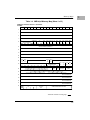
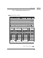
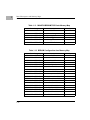
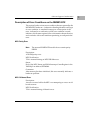
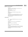
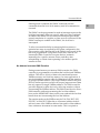
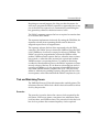
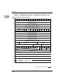
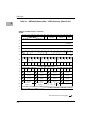
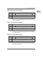
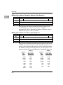
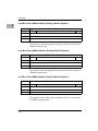
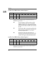
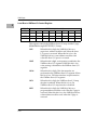
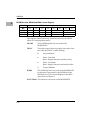
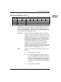
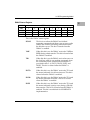
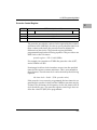
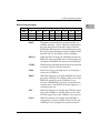
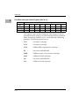
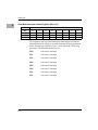
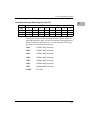
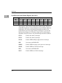
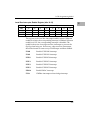
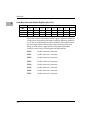
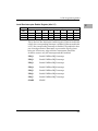
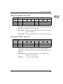
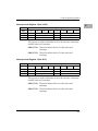
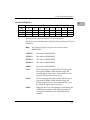
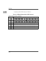
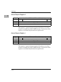
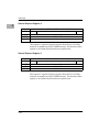
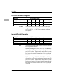
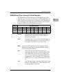
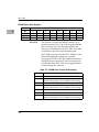
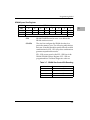
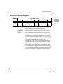
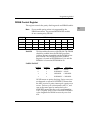
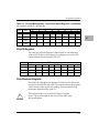
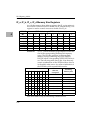
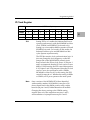
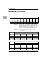
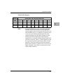
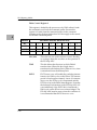
Access and Watchdog Time Base Select Register
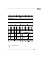
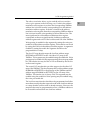
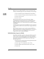
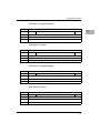
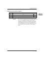
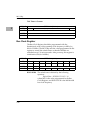
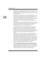
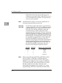
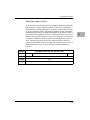
The watchdog timer control logic in the MC2 chip is used with the
ÒNo VMEbus InterfaceÓ option. This function is duplicated at the
same bit locations in the VMEchip2 at location $FFF4004C. It is
permissible to enable the watchdog timer in both the VMEchip2
and the MC2 chip.
3
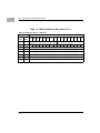
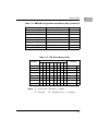
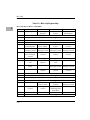
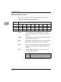
ADR/SIZ
BIT
$FFF42044 (8 bits)
15
14
13
NAME
11
10
9
LBTO
WDTO
OPER
R/W
R/W
R/W
RESET
0
0 PL
0 PL
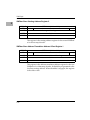
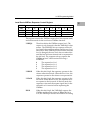
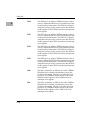
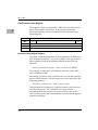
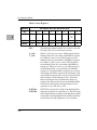
WDTO
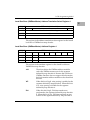
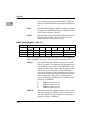
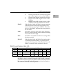
LBTO
8
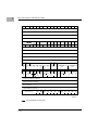
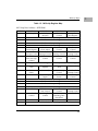
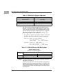
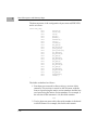
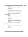
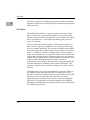
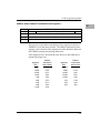
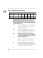
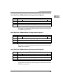
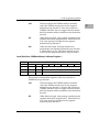
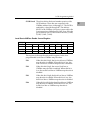
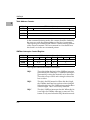
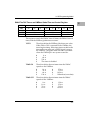
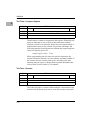
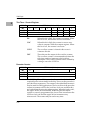
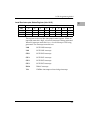
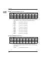
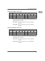
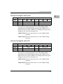
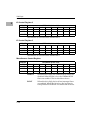
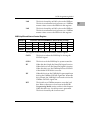
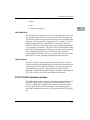
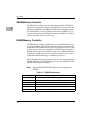
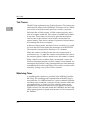
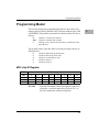
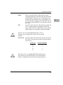
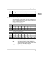
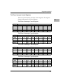
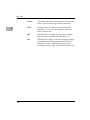
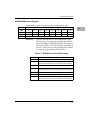
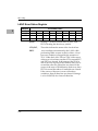
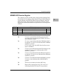
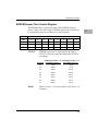
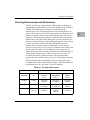
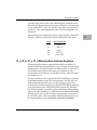
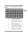
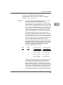
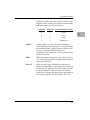
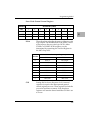
These bits define the watchdog time-out period:
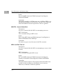
Bit Encoding
0
1
2
3
4
5
6
7
Time-out
512 µs
1 ms
2 ms
4 ms
8 ms
16 ms
32 ms
64 ms
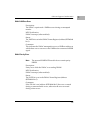
Bit Encoding
8
9
10
11
12
13
14
15
Time-out
128 ms
256 ms
512 ms
1 s
4 s
16 s
32 s
64 s
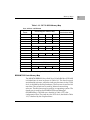
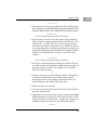
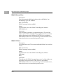
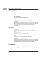
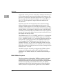
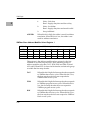
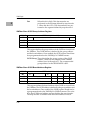
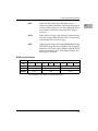
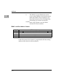
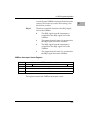
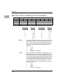
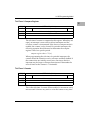
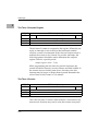
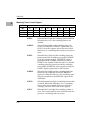
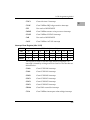
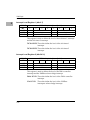
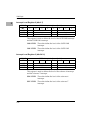
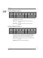
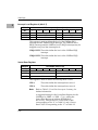
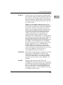
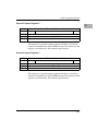
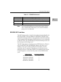
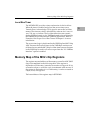
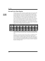
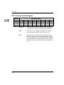
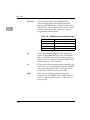
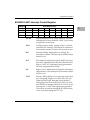
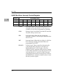
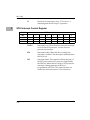
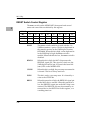
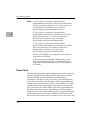
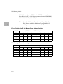
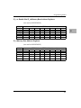
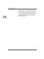
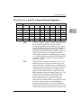
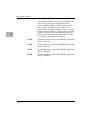
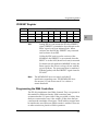
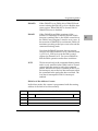
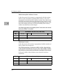
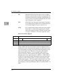
These bits define the local bus time-out value. The
timer begins timing when TS is asserted on the local
bus. If TA or TAE is not asserted before the timer
times out, a TEA signal is sent to the local bus. Note
that the Version Register bit V1 must be set to a 1 to
enable the MC2 chip access timer (i.e., it must be a
ÒNo VMEbus InterfaceÓ option).
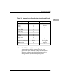
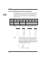
0
1
2
3
3-46
12
8 µs
64 µs
256 µs
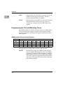
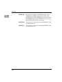
The timer is disabled.