1
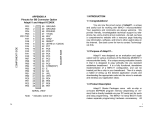
EAS FINGER BOARD II
68HC11
Single Board Computer
Ver. 11/24/03
Embedded Acquisition Systems
2517 Cobden Drive
Sterling Heights, MI
48310
http://www.embeddedtronics.com
email [email protected]
copyright 2003
All trademarks are those of their respective companies
1
EAS FINGER BOARD was created as a small compact general purpose embedded controller to be
used for robotics, data logging, smart instruments, and custom control applications. It can run
“Interactive C” and emulates many of the hardware functions of “Handy Board” by MIT. Motor
functions as well as push buttons were left out of the design to keep it small, simple and versatile. All
functions of the “Handy Board” can be added via expansion board, circuits of older “Rug warrior”
designs as well. The Finger Board uses very common easily found parts and a low parts count to
keep costs down. All mating contacts are spaced .1” apart to allow the Finger Board to plug on top of
standard prototyping boards. The Finger Board comes as two separate circuit boards, the CPU board
and the Communications board. It can be ordered as one board if size is not an issue.
FINGER BOARD II ASSEMBLY
Construction notes
This kit requires good soldering techniques due to its small size.
Tools necessary: A fine tip soldering gun and a good wire cutter.
Recommended tools: Mechanical clamp-known as a third hand, fine solder wick to remove excess
solder. A good source of information for beginners is found on the “Handy Board” web site.
An online construction manual with images is available on our web site to help in the construction of
the Finger Board. A copy of the Finger Board schematic, silkscreen and parts placement guide can
also be downloaded from our web site and printed out.
Caution: Integrated circuits are static and heat sensitive. Do not apply too much heat with your
soldering iron when installing these parts. Please take precautions while handing IC’s. To protect
against static electricity, ground your body before handling parts.
We will start with the CPU board first.
CPU Board
Step 1
Start by installing the IC's. Observe proper orientation for pin 1. You may install an IC socket for U7
and U6 but do not socket U5. The installation of a socket for U5 will interfere with U3, the 256kbit ram,
which will require the need for a socket. We normally do not install sockets for these IC's.
U5 - 74HC573
U6 - 74HC00
U7 - 74HC138
Step 2
Install capacitor C6 and the 28 pin IC socket for U3. You may need to snip off the center plastic
section of the IC socket so it will fit over U5.
C6 - .1uf monolithic capacitor. The printed value on the capacitor will normally be 104, denoting a .1uf
value.
U3 - 28pin IC socket
2
Step 3
Install the 52pin PGA IC socket for U4. Observe proper orientation for pin 1 before soldering.
Step 4
Install the resistors R2, R3, R5, R6 and R8. Bend the resistor so that it may stand end up on the PCB.
R2, R5, R6, R8 - 10K ohm
R3 - 1 Meg ohm
Step 5
Install resistor R4. This is a 47K inline sip resistor. Observe proper orientation for pin 1 before
soldering. Pin 1 is usually marked with a dot.
R4 - 47K ohm inline sip resistor. Part#10-1-473
Step 6
Install capacitor C3 and C4.
C3, C4 - 22pf capacitor (20pf may be substituted)
Step 7
Install capacitor C1, C2, C3, C5 and C7. Observe the polarity for C1. Place positive side closest to the
silkscreened "+" symbol.
C1 - 1uf tantalum, 25 volts or greater
C2, C5, C7 - .1uf monolithic. The printed value on the capacitor will normally be 104, denoting a .1uf
value.
Note: R1 and C13 are no longer needed
Step 8
Install diodes D2 and D3. Observe proper orientation. Place the cathode side of the diodes to line up
with the silkscreened bar on the PCB.
D2 - 1N4007 or 1N5817
D3 -1N4148
Note:
1N5817 has a lower voltage drop while the 1N4007 can handle more current, your choice
You can omit diode D2 and use solder pad J4 to bridge the connection. We recommend installing D2.
This will protect the Finger Board from reverse input supply voltage connections. J4 is located on the
bottom side of the board, near JP1.
Step 9
The following headers are normally installed on the topside of the Finger Board. Depending on user
applications all or none of the headers may be soldered in.
Headers are usually purchased in longer lengths and cut down to the size needed. Use headers with
a contact lead length of .230"(shorter style).
JP1 - 2 terminal block connector
JP2 - Header 7x2
3
JP6 - Header 2x2
JP10, JP12, JP13 - installed as one Header 3x2
JP14 - Header 3x2
JP18 - Header 2x1
JP19 - Header 2x1
Note:
If you have the one piece Finger Board with attached Communications board, you do not have to
install JP14. There are already pcb traces connecting JP14 to JP15.
You can omit JP6 and use the solder pads J1 and J2. By bridging solder pad J1, A/D ref input VRH
will be connected to VCC. Bridging solder pad J2 will connect A/D ref input VRL to ground. These two
pads are located on the bottom side of the board, near JP6.
Step 10
The following headers are normally installed on the bottom side of the Finger Board so that
prototyping boards can be used. Depending on your actual application, these headers can be placed
on top. Trim any excess lead lengths at this time before installing the headers.
JP4 - Header 4x2
JP7 - Header 8x2
JP9 - Header 10x2
JP11, JP8, JP17, JP16 - installed as one Header 12x2
Step 11
Install reset IC U1 and 5 volt regulator U2. Observe the silkscreened symbols on the PCB for proper
placement.
U1 - Dallas Semiconductor DS1233m (Note: DS1233 can be used, but its pins are different from the
DS1233m and will need to be oriented correctly)
We are currently replacing mc34064 with Dallas DS1233 from JDR Microdevices. We are still looking
for a source for the DS1233m, this is an equivalent part but has the same pin configuration as the
mc34064. The DS1233 is a far superior reset chip, we are very happy with the results and highly
recommend it over the mc34064. It will also reduce your parts count. If you are using the DS1233, you
will need to put the part in backwards and move the center pin to pin 1-square pad on the board. You
should also put a sleeve to prevent the wires from touching. (ie. pin1 now goes to pin 3 on the pcb
board, 2=>1, 3=>2). If you have the DS1233m, no changes are needed since it is a replacement for
the mc34064. We have provided a picture of this on our web page, under What's New.
U2 - LM7805
Note:
A low drop-out (LDO) voltage regulator can be substituted for the standard LM7805 regulator.
Applications that require low current use such as a solar cell powered Finger Board or running off 4
cell batteries may need a LDO regulator. If you install a LDO regulator, omit diode D2 and bridge
solder pad J4. The diode voltage drop will interfere with the LDO lowest voltage regulation. J4 is
located on the bottom side of the board, near JP1.
Step 12
Install crystal Y1. Cut a small piece of Mylar or thin cardboard insulation to prevent a short on the pc
board. Punch two small holes for the crystal leads so the insulator can fit against the bottom.
Y1 - 8Mhz crystal
4
Step 13
Bridge solder Pad J5 using a small blob of solder. This will connect the SRAM supply to VCC. J5 is
located on the bottom side of the board, near JP4.
Note:
If you plan to use a standard 256kbit SRAM memory chip and not a Dallas battery backed memory
module, do not bridge solder pad J5. See step 22 for optional external SRAM battery backup.
Step 14
You should wash and clean the completed board before installing U3 and U4. We use water soluble
flux solder here at EAS. This permits easy board cleaning. Radio Shack sells flux removing solvent
made for pc board cleaning. Take a close look at all solder joints and touch-up any joints that look
bad. A 2x or 3x magnifying glass helps to find any solder bridges.
When installing the 68HC11 processor, observe pin one polarity. Some PLCC sockets may require
firm pressure when pushing in the processor. Also observe proper pin placement when install the
memory module.
U4 - MC68HC11A1FN CPU
U3 - DS1230AB/Y Dallas 256kbit (32Kbyte) battery backed static ram. Substitute a DS1244Y if a real
time clock is needed. You can also use a Dallas DS1216D 28pin lithium battery socket but will need
separate 256kbit 62256-100LP static memory chip.
Note:
If you are using a header for JP6, place a couple of jumper shunts on JP6. This is the A/D reference
input voltage. Install a shunt across pins 1 and 2 to tie VRH to VCC. Install a shunt across pins 3 and
4 to tie VRL to ground.
A small hole is provided underneath the 68HC11 to be used to remove the processor. Use a small
diameter screwdriver to push the processor out of the IC socket.
Communications Board Assembly
Step 15
Install U8 on the Communications printed circuit board. Observe proper orientation for pin 1. If you
want, you can install an IC socket for U8.
U8 - MAX232CPE (Maxim)
Note: We have noticed when using 3rd party manufactured equivalent Maxim MAX232CPE chips,
downloading S19 files from DOS isn’t as reliable. Please purchase exact Maxim part for the
Communications Board.
Step 16
Install capacitors C8, C9, C10, C11, C12. Observe the polarity of the capacitors before soldering.
C8, C9, C10, C11, C12 - 1uf tantalum 16 volt or greater.
Step 17
Install resistor R7 and LED D1. The shorter lead on LED D1 is the cathode. If D1 is installed
5
backwards, the communications board will not operate. Place the cathode side of the LED to line up
with the silkscreened bar on the PCB.
R7 - 1K ohm
D1 - HLMP1790 LED
Note:
The LED is rated for 2ma. If a higher current model is substituted, the Communications board will not
work. You can decide not to install the LED, since it just indicates download mode. The download
mode will also be indicated on your computer screen while Interactive C is sending out the pcode.
Tech America (1-800-877-0072) sells a 3ma LED (model#90-1555) that can be substituted for the
HLMP-1790. The resistor R7 value must be increased to 2.2K, or else the current drain from the LED
will prevent communications
Step 18
Install switch S1 and S2.
S1, S2 - momentary normally open push button switch.
Use the middle two sets of holes on the PCB when installing the switches.
Step 19
Install connector P1 and header JP15.
P1 - Female DB9 pin connector
JP15 - Header 3x2
Note:
If you have the one piece Finger Board with attached Communications board, you do not have to
install JP15. There are already pcb traces connecting JP14 to JP15.
Step 20
To connect the main CPU board to the Communications board, you will need a short length of ribbon
cable and two female IDC connectors (3x2). When making the cable, make sure pin 1 line up together
on both connectors. The ribbon cable length should be no more than 1 foot between the CPU board
and Communications board. Serial communication errors may occur if cable is too long due to noise.
If you need a longer length from your computer to the Finger Board, then increase the length of cable
going from the Communications board to the PC serial port, since this length can be as long as 25ft.
Step 21
When using Interactive C, the Finger Board supports a 16x2 line LCD module connected to header
JP2. To connect the LCD module, you will need a short length of ribbon cable and two female IDC
connectors (7x2). When making the cable, make sure pin 1 line up together on both connectors. The
ribbon cable length should be no more than 1 foot.
Note:
If you cannot locate a LCD module, you can purchase one directly from EAS. The cable is included in
the price.
6
The Finger Board II was designed to allow our LCD module to mount directly on top using a header
and socket with the communications board attached.
Optional parts installation
Step 22 SRAM Battery Backup
If you plan to use a standard 256kbit SRAM memory chip and not the Dallas battery backed memory
module, install diodes D4 and D5. Place the cathode side of the diodes to line up with the
silkscreened bar on the PCB.
Do not bridge solder pad J5.
D4, D5 – IN5817
Note:
Placing a 3 to 5 volt battery on header JP19 will retain the SRAM memory when the main supply
voltage is disconnected. We do recommend using the Dallas battery backed memory chip, as it is
very reliable. However if you do use standard SRAM memory, use a good quality on/off switch for the
power. Power cycle switch bounce can corrupt the data in memory.
Step 23 Remote Serial Reset
To use the remote serial port reset feature, install mosfet Q1 and bridge solder pad J3.
Q1 - BS170 or MOSFET N
Note:
If you plan to use Interactive C, do not implement this feature
7
PARTS LIST FOR FINGER BOARD II
Bill Of Materials, all parts can be found from Radio Shack, Digikey, JDR and Jameco. All resistors ½
Watt or less. All similar parts found on “Handy Board” can also be used on Finger Board.
Item #
1
2
3
4
5
6
7
8
9
10
Quantity
1
4
2
5
11
7
12
13
14
15
16
17
18
19
20
21
22
23
24
1
1
2
2
1
2
4
1
1
1
JP10,JP12,JP13, JP16
JP17,JP18,JP19
JP2
JP4
JP6,JP11
JP7,JP8
JP9
JP14,JP15
J1,J2,J3,J4,J5
P1
Q1
R2,R5,R6,R8
R3
R4
R7
25
2
S1,S2
26
1
U1
27
28
1
1
U2
U3
29
30
31
32
33
34
35
36
37
38
39
40
41
42
1
1
1
1
1
1
1
1
2
1
U4
U5
U6
U7
U8
Y1
IC socket
IC socket
1
1
1
1
1
1
Part Reference #
C1
C2,C5,C6,C7
C3,C4
C8,C9,C10,C11,C12
C13
D1
D2
D3
D4,D5
JP1
Description
1uf tantalum capacitor, 25 volts or greater
.1uf monolithic capacitor
22pf capacitor (20pf can be substituted)
1uf tantalum capacitor, 16 volts or greater
Note: C13 is no longer needed
HLMP-1790 LED (2ma rating)
1N4007 or 1N5817
1N4148
1N5817 (optional, only for external SRAM battery backup)
OST 2 terminal block connector 3.5mm lead spacing.
Digikey Part#ED1514-ND
Header 2x1 (all headers are .1" straight male double row
Jameco Part#103405 - snap apart to correct length)
Header 7x2
Header 4x2
Header 2x2
Header 8x2
Header 10x2
Header 3x2
Solder Pads (on PCB, not a part)
Female DB9 pin connector short profile
BS170 or MOSFET N (optional, for remote serial reset)
10K ohm resistor
1Meg ohm resistor
47Kohm 10 pin inline resistor pack. (Part# 10-1-473)
2.2K ohm resistor model#90-1555 LED (3ma) or
1K ohm resistor HLMP-1790 LED (2ma rating)
Momentary normally open push button switch
Digikey Part# SW263CT-ND
DS1233m (Note: DS1233 can be used, but its pins are
positioned differently from the DS1233m)
LM7805 or LM340T (+5 volt regulator)
DS1230AB/Y Dallas 256kbit (32Kbyte) battery backed static
ram. Substitute a DS1244Y if a real time clock is needed.
You can also use a Dallas DS1216D 28 pin lithium battery
socket but will need separate 256kbit 62256-100LP static
memory chip
MC68HC11A1FN CPU (Motorola)
74HC573
74HC00
74HC138
MAX232CPE (Maxim)
8Mhz Crystal - Series
28 pin socket
52 pin PLCC socket
3x2 Female IDC connectors
Ribbon cable - 6" length , 6 conductor
16x2 character LCD module
Beeper 5Volt TTL or speaker
3 Volt Battery (optional external battery for SRAM backup)
Finger Board II printed circuit board
Optional
Optional
BT1
PCB
Optional items not included:
½" 4-40 plastic standoffs for mounting, 2 jumper shunts for JP6
Use headers with a contact lead length of .230"(shorter style) for expansion boards.
Prototype expansion board with .1" spacing, can be found at your local Radio Shack.
8
CONNECTING TO THE FINGER BOARD
9
Headers are counted in the same pattern as drawn on the schematic diagram. When possible we
have placed the label closest to pin 1 on the printed circuit board. Pin 1 is marked with a square pad.
See silkscreen top view drawing.
JP1 is the DC input connector used to power the Finger Board. You can use any voltage from 7 to 18
volts.
Pin
1
2
Function
+Battery input
ground
JP2 is an Interactive C compatible LCD interface. If you have the 14 x 1 type connector on your LCD,
you should be able to rewire with the pattern shown.
Pin
1
3
5
7
9
11
13
Function
ground
ground
A8
D0
D2
D4
D6
Pin
2
4
6
8
10
12
14
Function
VCC
A9
PA4
D1
D3
D5
D7
JP4 is an SPI high-speed serial peripheral interface. There are lots of industry SPI compatible devices
that can be attached to this port.
For those who wish to connect two Finger Boards together using the SPI port, you must not connect
pin 2 (VCC) together between the Finger Boards. Doing so will short out the voltage regulators. You
can use a straight through IDC ribbon cable but cut out pin 2 from one or both of the JP4 headers.
For other SPI devices, pin 2 can be used to supply +5 volt power. The 5 volt source is taken from the
onboard 7805 voltage regulator.
Pins 7 and 8 on the header are not connected. They can be wired up to user determined chip selects.
Pin
1
3
5
7
Function
ground
SS
SCK
n/c
Pin
2
4
6
8
Function
VCC
MISO
MOSI
n/c
n/c not connected
JP6 analog A/D reference input voltage. For normal use, pins 1 and 2 are shorted and pins 3 and 4
are shorted together using jumper shunts. See "M68HC11 Reference Manual" for further info.
Pin
1
3
Function
VRH
VRL
Pin
2
4
Function
VCC
ground
10
JP7 is the 68HC11 8-bit A/D analog input port. Input voltages between 0 and 5volts can be applied to
the A/D. Grounds are provided for each analog input.
Pin
1
3
4
6
7
9
11
13
Function
AN0
AN1
AN2
AN3
AN4
AN5
AN6
AN7
Pin
2
3
5
6
8
10
12
14
Function
ground
ground
ground
ground
ground
ground
ground
ground
JP8 is PORT A on the 68HC11. This is an 8-bit digital input/output port. Reading the "M68HC11
Reference Manual", by Motorola will give information on how to utilize this port. In Interactive C, some
of these pins are pre-assigned. By editing the library routines, you can change the pre-assigned
functions.
Pin
1
3
5
7
9
11
13
15
Function
PA0
PA1
PA2
PA3
PA4
PA5
PA6
PA7
Pin
2
4
6
8
10
12
14
16
Function
ground
ground
ground
ground
ground
ground
ground
ground
JP9 is the expansion bus. It is setup so you can easily enhance the Finger Board with additional
circuits. You can have up to 32 memory mapped digital inputs and 32 digital outputs. Circuit diagrams
are available at our Web page on how to utilize this header. Data lines are brought out as well as
power and ground pins. Hexadecimal address map is shown. W is for write; R is for read.
CPU address lines A0 and A1 are available for memory mapped LCD's or other peripheral devices.
Pin
1
3
5
7
9
11
13
15
17
19
Function
4000W 2
4000R
5000W 6
5000R
6000W 10
6000R
7000W 14
7000R
A0
VCC
Pin
D0
4
D2
8
D4
12
D6
16
18
20
Function
D1
D3
D5
D7
A1
ground
11
JP10 is a dedicated header for a Sharp IR receiver when running Interactive C.
Pin
1
2
Function
Sharp IR receiver (68HC11 output pin PA2)
Ground
JP11 is useful for external interrupt requests.
Pin
1
3
Function
XIRQ\
IRQ\
Pin
2
4
Function
ground
ground
JP12 is a dedicated header for a Piezo beeper or speaker when running Interactive C.
Pin
1
2
Function
+ Piezo beeper or speaker (68HC11 output pin PA3)
ground
JP13 is a dedicated header for an Infrared transmitter when running Interactive C.
Pin
1
2
Function
Infrared transmitter (68HC11 output pin PA6)
ground
JP14 is the serial communications header on the CPU board that is used to connect to the
Communications Board.
Pin
1
3
5
Function
PD0
PD1
ground
Pin
2
4
6
Function
MODA
reset
VCC
JP15 is the serial communications header on the Communications board that is used to connect to
the main CPU board.
Pin
1
3
5
Function
PD0
PD1
ground
Pin
2
4
6
Function
MODA
reset
VCC
JP16 is an available 5volt source (VCC) taken from the onboard 7805 voltage regulator.
Pin
1
2
Function
VCC
Ground
JP17 is used to connect an external reset switch.
Pin
1
2
Function
reset
ground
12
JP18 is the MODB select. By placing a jumper on JP18, this will enable you to change the reset
vector from 0xBFFE, 0xBFFF to 0xFFFE,0xFFFF. It is used in conjunction with the Download switch
(S1) on the Communications board. Pressing the Download switch pulls the MODA line low (open).
Pin
1
2
Function
MODB
VCC
CPU Hardware Mode select summary
JP18
Download Switch S1 (default is closed, pressing S1 opens)
MODB
MODA
closed
closed
Normal Expanded (reset at 0xFFFE,0xFFFF)
open
open
Special Bootstrap (for downloading programs into memory)
open
closed
Special Test (Default mode for Interactive C, reset at 0xBFFE, 0xBFFF)
JP19 is used to connect an external battery for SRAM battery backup. Use a 3-5 volt battery. This is
not needed if you use a Dallas battery backup memory module.
Pin
1
2
Function
+BT1 3-5Volt battery
ground
P1 is the Communications board DB9 RS232 connector. It is a simple three wire asynchronous serial
interface. When using Interactive C, set your PC serial port to 9600 baud, 1 start, 1 stop, 8 data, no
parity. Use a standard serial cable to connect the PC serial port to the Finger Board. If your PC has a
25 pin serial port, use a 9 to 25 pin adapter.
Pin
1
2
3
4
5
6
7
8
Function
n/c
TxD
RxD
n/c
ground
n/c
RTS
CTS
n/c not connected
13
RUNNING INTERACTIVE C
Interactive C (IC) is a simple to use C compiler for the 68HC11. The freeware version of IC can be
downloaded from MIT’s FTP site at
ftp://cherupakha.media.mit.edu/pub/projects/6270/interactive-c along with a manual that
can be printed out for reference. There is also more information on the “Handy Board” web page on
how to use IC.
To use the Finger Board you need to connect the serial port of your PC to the serial connector P1 of
the Finger Board Communications board. You should be able to run version 2.86 or the newest
commercial version of IC from Newton Labs, but you must load the “Rug Warrior” version of the
pcode.
The MODB setting (JP18) should be un-jumpered. This sets the 68HC11 CPU in “Special Test Mode”
with a reset vector address location of $BFFE:BFFF. Interactive C will not run if JP18 is jumpered.
When using version 2.86. Make sure ic.exe is set. Example setup by executing “ic -config” is shown:
C:\IC>ic -config
Interactive C for 6811. Version 2.860 BETA (Nov 29 1994)
IC written by Randy Sargent and Anne Wright. Copyright 1994.
(uses board pcode by R. Sargent, F. Martin, and A. Wright)
This program is freeware and unsupported. It is provided as a service to
hobbyists and educators. Type 'about' for information about support
and obtaining newer versions of IC.
Backing up C:\IC\IC.EXE to C:\IC\IC.bak
Done
Default editor: edit
Directory where libraries reside: /ic/libs/
Default library file (blank for none): /ic/libs/lib_rw11.lis
Default serial device name (in the form /dev/*): com1
Finished configuring
Note: lib_rw11.lis should be edited if you need to add additional library routines. The nicest thing
about 2.860 is all source code is made public and can be recompiled.
To put Finger Board in download mode. You need to hit the reset switch or just re-power Finger Board
while pressing the download push button S1 on the Communications board. Once you release the
download push button S1, the LED D1 will turn off, indicating that the board is in download mode. This
LED works the same as on the “Handy Board”. Note: If you are using a reset switch you must release
the reset switch first then release the download push button S1. Initially, the LED may not be on, once
initial communications is established it will function normally.
14
USING OTHER COMPILERS AND PROGRAMS
The Finger Board was designed to take advantage of the many public domain software available on
the web as well as any commercial compilers. There are links on our web site to freeware and
shareware compilers and programs that can be downloaded and used to write programs for the
Finger Board II. Check out our related sites page for links to commercial compilers
To use certain compilers, you must be aware of the reset vector location. The reset vector address
can be changed by jumping JP18. The default mode of operation for Interactive C is "Special Test
Mode" and the reset vector is located at address $BFFE:BFFF. By jumping JP18, the reset vector
location can be set to address $FFFE:FFFF. Read the “M68HC11 Reference Manual” by Motorola for
a better description.
You can use DL.EXE (found in Interactive C) to download compiled S19 records to the Finger Board.
There are other C compilers for the 68HC11 that can be used, Small C, ICC11, and GCC. For BASIC
programs, use SBasic by Karl Lunt. Karl also has written a version of FORTH for the HC11 called
tiny4th. Two very good interactive debuggers are NoICE by John Hartman and PCbug
(Pcbug342.exe) by Motorola. A good bootloader is Hcload by Sylvain Bissonnette. The one we have
found to be very reliable is DL68hc11 by Wilfried Markenstein. Motorola also has a freeware
assembler, as11.
15
FREQUENTLY ASKED QUESTIONS (FAQ)
Please check our web site for the latest version of the Finger Board FAQ.
TROUBLE SHOOTNG
If you have purchased the assembled Finger Board, it is fully tested and operational before shipping.
If it fails to function properly, inspect the board for obvious physical damage. If there is damage,
please contact us for replacement.
The most common problems are improperly configured communications parameters or attempting to
use the wrong COM port on the PC. Verify that your communications port is working by substituting a
known good serial device or by doing a loopback diagnostic. Also check your power source. The
input voltage should not fall below 7 volts DC.
For kits,
Check for +5VCC voltage on header JP16.
Check and make sure all components are installed and properly orientated.
Check all resistor and capacitor values.
Check LED polarity.
Check IC positions.
Check Tantalum capacitor polarities.
Check for shorts.
Check for cold solder joints.
Problems communicating, remove LED D1, it’s probably in backwards.
If not using the optional SRAM battery backed feature, makes sure solder pad J5 is bridged.
16
Silkscreen Top View. Pin 1 on all headers are indicated by the square pad.
Parts placement
17
SPECIFICATIONS:
Motorola 68HC11 CPU A0, A1, A8, E2, or E9 versions can be used.
256kbit (32Kbyte) Dallas 10 year battery-backed memory module, no need to use EPROMs or slower
EEPROMs.
Compact size 2” X 2.85”.
Interactive C compatible LCD interface.
Network capable, Serial Peripheral Interface (SPI).
Jumper selectable reset address. Reset vector can be located at 0xFFFE,0xFFFF or 0xBFFE,0xBFFF
improved over the Handy Board.
No expensive hardware programmer needed, programs can be downloaded using a standard serial
port.
Easily expandable, using standard headers. List of Headers:
Port A of 68HC11, 8 multi function I/O pins (JP8)
Port E of 68HC11, 8 analog channels (JP7)
Memory mapped I/O, Finger Board can be easily expanded to have 32 digital inputs and 32 digital
output lines (JP9)
IRQ and XIRQ lines brought out for external interrupts (JP11)
Standard 9pin serial port (P1).
SPI high speed serial interface (JP4)
LCD display interface (JP2)
Sharp IR receiver input (JP10)
Speaker output (JP12)
Infrared transmitter output (JP13)
MODB select (JP18)
External A/D reference input (JP6)
Optional external battery backup capable (JP19)
Optional Low Dropout voltage regulator
Optional remote reset through serial port
Optional real time clock
Power requirements:
7 to 18volts DC. Can easily run from a 9volts DC battery.
Current consumption: 24 ma DC without communications board < 10ma in WAIT mode, or STOP
mode. 30ma with communications board
For remote data logging - using an Alkaline 9volt battery to supply power, we were able to get 19
hours using the Finger Board without the communications board, but with an attached LCD for
display. The total current draw was ~25 ma. The LCD display typically draws about ~1ma.
For low battery situations and Solar Cell applications. Special modifications can be made to the
Finger Board. With a few easy component changes, we were able to bring the current draw down to
22ma. By changing the voltage regulator to a low dropout version, the Finger Board was able to run
from 26volts down to 4.8volts. These application specific modifications are posted on our web site.
Dimensions:
CPU board only: 2.85” long, 2.0” wide
Communications board: 1.15” long, 2.0” wide
CPU board with attached Communications board: 4” long, 2.0” wide
18
STANDARD LEGAL STUFF
Although all of the circuits and projects provided have been thoroughly tested by Embedded Acquisition
Systems (EAS). We cannot take responsibility for the circuits, nor will we take any responsibility for anything
happening as a result of using any of our designs.
PERFORMANCE INFORMATION: Performance tests and ratings are measured using specific computer
systems and/or components and reflect the approximate performance of EAS
products as measured by those tests. Any difference in system hardware or software design or configuration
may affect actual performance.
SINGLE COPY LICENSE: You may download copies of the information or software ("Materials") found on EAS
sites on a single computer for your personal, non-commercial internal use only. This is a license, not a transfer
of title, and is subject to the following restrictions: you may not: (a) modify the Materials or use them for any
commercial purpose, or any public display, performance, sale or rental; (b) decompile, reverse engineer, or
disassemble software Materials; (c) remove any copyright or other proprietary notices from the Materials; (d)
transfer the Materials to another person. You agree to prevent any unauthorized copying of the Materials.
OWNERSHIP OF MATERIALS: Materials are copyrighted and are protected by worldwide copyright laws and
treaty provisions. They may not be copied, reproduced, modified,
published, uploaded, posted, transmitted, or distributed in any way, without EAS's prior written permission.
Other rights may be granted to you by EAS in writing or incorporated elsewhere in the Materials.
TERMINATION OF THIS LICENSE: EAS may terminate this license at any time if you are in breach of the terms
of this Agreement. Upon termination, you will immediately destroy the Materials.
DISCLAIMER: The materials are provided "as is" without any express or implied warranty of any kind including
warranties of merchantability, noninfringement of intellectual property, or fitness for any particular purpose. In no
event shall EAS, or its suppliers be liable for any damages whatsoever (including, without limitation, damages
for loss of profits, business interruption, loss of information) arising out of the use of or inability to use the
materials, even if EAS has been advised of the possibility of such damages.
BECAUSE SOME JURISDICTIONS PROHIBIT THE EXCLUSION OR LIMITATION OF LIABILITY FOR
CONSEQUENTIAL OR INCIDENTAL DAMAGES, THEABOVE LIMITATION MAY NOT APPLY TO YOU.
EAS further does not warrant the accuracy or completeness of the information, text, graphics, links or other
items contained within these materials. EAS may make changes to these materials, or to the products described
therein, at any time without notice. EAS makes no commitment to update the Materials.
19
PARTS LIST FOR FINGER BOARD II
Bill Of Materials, all parts can be found from Radio Shack, Digikey, JDR and Jameco.
All resistors ½ Watt or less. All similar parts found on “Handy Board” can also be used on Finger
Board.
Item #
1
2
3
4
5
6
7
8
9
10
Quantity
1
4
2
5
11
7
12
13
14
15
16
17
18
19
20
21
22
23
24
1
1
2
2
1
2
4
1
1
1
JP10,JP12,JP13, JP16
JP17,JP18,JP19
JP2
JP4
JP6,JP11
JP7,JP8
JP9
JP14,JP15
J1,J2,J3,J4,J5
P1
Q1
R2,R5,R6,R8
R3
R4
R7
25
2
S1,S2
26
1
U1
27
28
1
1
U2
U3
29
30
31
32
33
34
35
36
37
38
39
40
41
42
1
1
1
1
1
1
1
1
2
1
U4
U5
U6
U7
U8
Y1
IC socket
IC socket
1
1
1
1
1
1
Part Reference #
C1
C2,C5,C6,C7
C3,C4
C8,C9,C10,C11,C12
C13
D1
D2
D3
D4,D5
JP1
Optional
Optional
BT1
PCB
Description
1uf tantalum capacitor, 25 volts or greater
.1uf monolithic capacitor
22pf capacitor (20pf can be substituted)
1uf tantalum capacitor, 16 volts or greater
Note: C13 is no longer needed
HLMP-1790 LED (2ma rating)
1N4007 or 1N5817
1N4148
1N5817 (optional, only for external SRAM battery backup)
OST 2 terminal block connector 3.5mm lead spacing.
Digikey Part#ED1514-ND
Header 2x1 (all headers are .1" straight male double row
Jameco Part#103405 - snap apart to correct length)
Header 7x2
Header 4x2
Header 2x2
Header 8x2
Header 10x2
Header 3x2
Solder Pads (on PCB, not a part)
Female DB9 pin connector short profile
BS170 or MOSFET N (optional, for remote serial reset)
10K ohm resistor
1Meg ohm resistor
47Kohm 10 pin inline resistor pack. (Part# 10-1-473)
2.2K ohm resistor model#90-1555 LED (3ma) or
1K ohm resistor HLMP-1790 LED (2ma rating)
Momentary normally open push button switch
Digikey Part# SW263CT-ND
DS1233m (Note: DS1233 can be used, but its pins are
positioned differently from the DS1233m)
LM7805 or LM340T (+5 volt regulator)
DS1230AB/Y Dallas 256kbit (32Kbyte) battery backed static
ram. Substitute a DS1244Y if a real time clock is needed.
You can also use a Dallas DS1216D 28 pin lithium battery
socket but will need separate 256kbit 62256-100LP static
memory chip
MC68HC11A1FN CPU (Motorola)
74HC573
74HC00
74HC138
MAX232CPE (Maxim)
8Mhz Crystal - Series
28 pin socket
52 pin PLCC socket
3x2 Female IDC connectors
Ribbon cable - 6" length , 6 conductor
16x2 character LCD module
Beeper 5Volt TTL or speaker
3 Volt Battery (optional external battery for SRAM backup)
Finger Board II printed circuit board
20