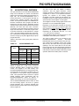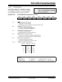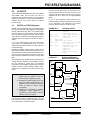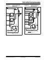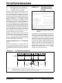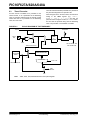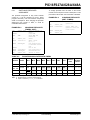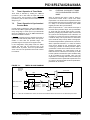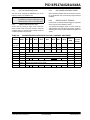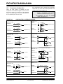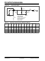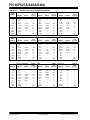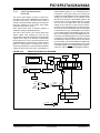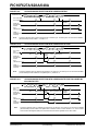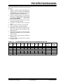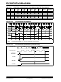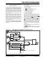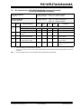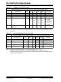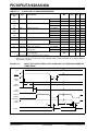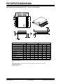
1
PIC16F627A/628A/648A Data Sheet Flash-Based 8-Bit CMOS Microcontrollers with nanoWatt Technology 2004 Microchip Technology Inc. Preliminary DS40044B Note the following details of the code protection feature on Microchip devices: • Microchip products meet the specification contained in their particular Microchip Data Sheet. • Microchip believes that its family of products is one of the most secure families of its kind on the market today, when used in the intended manner and under normal conditions. • There are dishonest and possibly illegal methods used to breach the code protection feature. All of these methods, to our knowledge, require using the Microchip products in a manner outside the operating specifications contained in Microchip's Data Sheets. Most likely, the person doing so is engaged in theft of intellectual property. • Microchip is willing to work with the customer who is concerned about the integrity of their code. • Neither Microchip nor any other semiconductor manufacturer can guarantee the security of their code. Code protection does not mean that we are guaranteeing the product as “unbreakable.” Code protection is constantly evolving. We at Microchip are committed to continuously improving the code protection features of our products. Attempts to break Microchip’s code protection feature may be a violation of the Digital Millennium Copyright Act. If such acts allow unauthorized access to your software or other copyrighted work, you may have a right to sue for relief under that Act. Information contained in this publication regarding device applications and the like is intended through suggestion only and may be superseded by updates. It is your responsibility to ensure that your application meets with your specifications. No representation or warranty is given and no liability is assumed by Microchip Technology Incorporated with respect to the accuracy or use of such information, or infringement of patents or other intellectual property rights arising from such use or otherwise. Use of Microchip’s products as critical components in life support systems is not authorized except with express written approval by Microchip. No licenses are conveyed, implicitly or otherwise, under any intellectual property rights. Trademarks The Microchip name and logo, the Microchip logo, Accuron, dsPIC, KEELOQ, MPLAB, PIC, PICmicro, PICSTART, PRO MATE, PowerSmart and rfPIC are registered trademarks of Microchip Technology Incorporated in the U.S.A. and other countries. AmpLab, FilterLab, microID, MXDEV, MXLAB, PICMASTER, SEEVAL, SmartShunt and The Embedded Control Solutions Company are registered trademarks of Microchip Technology Incorporated in the U.S.A. Application Maestro, dsPICDEM, dsPICDEM.net, dsPICworks, ECAN, ECONOMONITOR, FanSense, FlexROM, fuzzyLAB, In-Circuit Serial Programming, ICSP, ICEPIC, Migratable Memory, MPASM, MPLIB, MPLINK, MPSIM, PICkit, PICDEM, PICDEM.net, PICtail, PowerCal, PowerInfo, PowerMate, PowerTool, rfLAB, Select Mode, SmartSensor, SmartTel and Total Endurance are trademarks of Microchip Technology Incorporated in the U.S.A. and other countries. Serialized Quick Turn Programming (SQTP) is a service mark of Microchip Technology Incorporated in the U.S.A. All other trademarks mentioned herein are property of their respective companies. © 2004, Microchip Technology Incorporated, Printed in the U.S.A., All Rights Reserved. Printed on recycled paper. Microchip received ISO/TS-16949:2002 quality system certification for its worldwide headquarters, design and wafer fabrication facilities in Chandler and Tempe, Arizona and Mountain View, California in October 2003. The Company’s quality system processes and procedures are for its PICmicro® 8-bit MCUs, KEELOQ® code hopping devices, Serial EEPROMs, microperipherals, nonvolatile memory and analog products. In addition, Microchip’s quality system for the design and manufacture of development systems is ISO 9001:2000 certified. DS40044B-page ii Preliminary 2004 Microchip Technology Inc. PIC16F627A/628A/648A 18-pin Flash-Based 8-Bit CMOS Microcontrollers with nanoWatt Technology High Performance RISC CPU: Low Power Features: • • • • • • Standby Current: - 100 nA @ 2.0V, typical • Operating Current: - 12 µA @ 32 kHz, 2.0V, typical - 120 µA @ 1 MHz, 2.0V, typical • Watchdog Timer Current - 1 µA @ 2.0V, typical • Timer1 oscillator current: - 1.2 µA @ 32 kHz, 2.0V, typical • Dual Speed Internal Oscillator: - Run-time selectable between 4 MHz and 37 kHz - 4 µs wake-up from Sleep, 3.0V, typical Operating speeds from DC - 20 MHz Interrupt capability 8-level deep hardware stack Direct, Indirect and Relative Addressing modes 35 single word instructions - All instructions single cycle except branches Special Microcontroller Features: • Internal and external oscillator options - Precision Internal 4 MHz oscillator factory calibrated to ±1% - Low Power Internal 37 kHz oscillator - External Oscillator support for crystals and resonators. • Power saving Sleep mode • Programmable weak pull-ups on PORTB • Multiplexed Master Clear/Input-pin • Watchdog Timer with independent oscillator for reliable operation • Low voltage programming • In-Circuit Serial Programming™ (via two pins) • Programmable code protection • Brown-out Reset • Power-on Reset • Power-up Timer and Oscillator Start-up Timer • Wide operating voltage range. (2.0 - 5.5V) • Industrial and extended temperature range • High Endurance Flash/EEPROM Cell - 100,000 write Flash endurance - 1,000,000 write EEPROM endurance - 100 year data retention Device Program Memory Peripheral Features: • 16 I/O pins with individual direction control • High current sink/source for direct LED drive • Analog comparator module with: - Two analog comparators - Programmable on-chip voltage reference (VREF) module - Selectable internal or external reference - Comparator outputs are externally accessible • Timer0: 8-bit timer/counter with 8-bit programmable prescaler • Timer1: 16-bit timer/counter with external crystal/ clock capability • Timer2: 8-bit timer/counter with 8-bit period register, prescaler and postscaler • Capture, Compare, PWM module - 16-bit Capture/Compare - 10-bit PWM • Addressable Universal Synchronous/Asynchronous Receiver/Transmitter USART/SCI Data Memory I/O CCP (PWM) USART Comparators Timers 8/16-bit 128 16 1 Y 2 2/1 128 16 1 Y 2 2/1 256 16 1 Y 2 2/1 Flash (words) SRAM (bytes) EEPROM (bytes) PIC16F627A 1024 224 PIC16F628A 2048 224 PIC16F648A 4096 256 2004 Microchip Technology Inc. Preliminary DS40044B-page 1 PIC16F627A/628A/648A Pin Diagrams PDIP, SOIC 1 18 RA1/AN1 RA3/AN3/CMP1 2 17 RA0/AN0 16 RA7/OSC1/CLKIN 15 RA6/OSC2/CLKOUT 14 VDD 13 RB7/T1OSI/PGD 3 RA5/MCLR/VPP 4 RB0/INT 6 RB1/RX/DT 7 12 RB6/T1OSO/T1CKI/PGC RB2/TX/CK 8 11 RB5 RB3/CCP1 9 10 RB4/PGM RA5/MCLR/VPP 8 9 10 NC 11 12 RB4/PGM 13 RB5 NC 14 1 21 NC 2 20 VSS 3 19 NC 4 PIC16F627A/628A 18 NC PIC16F648A VSS 17 5 NC 6 16 RB0/INT 7 15 DS40044B-page 2 RA7/OSC1/CLKIN RA6/OSC2/CLKOUT VDD VDD RB7/T1OSI/PGD RB6/T1OSO/T1CKI/PGC RB1/RX/DT RB2/TX/CK RB3/CCP1 RA2/AN2/VREF RA3/AN3/CMP1 RA4/TOCKI/CMP2 RA5/MCLR/VPP VSS VSS RB0/INT RB1/RX/DT RB2/TX/CK RB3/CCP1 1 2 3 4 5 6 7 8 9 10 PIC16F627A/628A/648A 28 27 26 25 NC 24 23 22 NC RA4/T0CKI/CMP2 RA3/AN3/CMP1 RA2/AN2/VREF 28-Pin QFN 20 19 18 17 16 15 14 13 12 11 RA1/AN1 RA0/AN0 RA7/OSC1/CLKIN RA6/OSC2/CLKOUT VDD VDD RB7/T1OSI/PGD RB6/T1OSO/T1CKI/PGC RB5 RB4/PGM VSS 5 RA1/AN1 RA0/AN0 RA4/TOCKI/CMP2 PIC16F627A/628A/648A PIC16F627A/628A/648A SSOP RA2/AN2/VREF Preliminary 2004 Microchip Technology Inc. PIC16F627A/628A/648A Table of Contents 1.0 2.0 3.0 4.0 5.0 6.0 7.0 8.0 9.0 10.0 11.0 12.0 13.0 14.0 15.0 16.0 17.0 18.0 19.0 General Description...................................................................................................................................................................... 5 PIC16F627A/628A/648A Device Varieties ................................................................................................................................... 7 Architectural Overview ................................................................................................................................................................. 9 Memory Organization ................................................................................................................................................................. 15 I/O Ports ..................................................................................................................................................................................... 31 Timer0 Module ........................................................................................................................................................................... 45 Timer1 Module ........................................................................................................................................................................... 48 Timer2 Module ........................................................................................................................................................................... 52 Capture/Compare/PWM (CCP) Module ..................................................................................................................................... 55 Comparator Module.................................................................................................................................................................... 61 Voltage Reference Module......................................................................................................................................................... 67 Universal Synchronous Asynchronous Receiver Transmitter (USART) Module........................................................................ 69 Data EEPROM Memory ............................................................................................................................................................. 89 Special Features of the CPU...................................................................................................................................................... 93 Instruction Set Summary .......................................................................................................................................................... 111 Development Support............................................................................................................................................................... 125 Electrical Specifications............................................................................................................................................................ 131 DC and AC Characteristics Graphs and Tables....................................................................................................................... 147 Packaging Information.............................................................................................................................................................. 149 TO OUR VALUED CUSTOMERS It is our intention to provide our valued customers with the best documentation possible to ensure successful use of your Microchip products. To this end, we will continue to improve our publications to better suit your needs. Our publications will be refined and enhanced as new volumes and updates are introduced. If you have any questions or comments regarding this publication, please contact the Marketing Communications Department via E-mail at [email protected] or fax the Reader Response Form in the back of this data sheet to (480) 792-4150. We welcome your feedback. Most Current Data Sheet To obtain the most up-to-date version of this data sheet, please register at our Worldwide Web site at: http://www.microchip.com You can determine the version of a data sheet by examining its literature number found on the bottom outside corner of any page. The last character of the literature number is the version number, (e.g., DS30000A is version A of document DS30000). Errata An errata sheet, describing minor operational differences from the data sheet and recommended workarounds, may exist for current devices. As device/documentation issues become known to us, we will publish an errata sheet. The errata will specify the revision of silicon and revision of document to which it applies. To determine if an errata sheet exists for a particular device, please check with one of the following: • Microchip’s Worldwide Web site; http://www.microchip.com • Your local Microchip sales office (see last page) • The Microchip Corporate Literature Center; U.S. FAX: (480) 792-7277 When contacting a sales office or the literature center, please specify which device, revision of silicon and data sheet (include literature number) you are using. Customer Notification System Register on our web site at www.microchip.com/cn to receive the most current information on all of our products. 2004 Microchip Technology Inc. Preliminary DS40044B-page 3 PIC16F627A/628A/648A NOTES: DS40044B-page 4 Preliminary 2004 Microchip Technology Inc. PIC16F627A/628A/648A 1.0 GENERAL DESCRIPTION HS is for High-Speed crystals. The EC mode is for an external clock source. The PIC16F627A/628A/648A are 18-Pin Flash-based members of the versatile PIC16CXX family of low cost, high performance, CMOS, fully-static, 8-bit microcontrollers. All PICmicro® microcontrollers employ an advanced RISC architecture. The PIC16F627A/628A/648A have enhanced core features, eight-level deep stack, and multiple internal and external interrupt sources. The separate instruction and data buses of the Harvard architecture allow a 14-bit wide instruction word with the separate 8-bit wide data. The two-stage instruction pipeline allows all instructions to execute in a singlecycle, except for program branches (which require two cycles). A total of 35 instructions (reduced instruction set) are available, complemented by a large register set. PIC16F627A/628A/648A microcontrollers typically achieve a 2:1 code compression and a 4:1 speed improvement over other 8-bit microcontrollers in their class. PIC16F627A/628A/648A devices have integrated features to reduce external components, thus reducing system cost, enhancing system reliability and reducing power consumption. The PIC16F627A/628A/648A has 8 oscillator configurations. The single-pin RC oscillator provides a low cost solution. The LP oscillator minimizes power consumption, XT is a standard crystal, and INTOSC is a selfcontained precision two-speed internal oscillator. The TABLE 1-1: Clock Memory A highly reliable Watchdog Timer with its own on-chip RC oscillator provides protection against software lockup. Table 1-1 shows the features of the PIC16F627A/ 628A/648A mid-range microcontroller families. A simplified block diagram of the PIC16F627A/628A/ 648A is shown in Figure 3-1. The PIC16F627A/628A/648A series fits in applications ranging from battery chargers to low power remote sensors. The Flash technology makes customizing application programs (detection levels, pulse generation, timers, etc.) extremely fast and convenient. The small footprint packages makes this microcontroller series ideal for all applications with space limitations. Low cost, low power, high performance, ease of use and I/O flexibility make the PIC16F627A/628A/648A very versatile. 1.1 Development Support The PIC16F627A/628A/648A family is supported by a full-featured macro assembler, a software simulator, an in-circuit emulator, a low cost in-circuit debugger, a low cost development programmer and a full-featured programmer. A Third Party “C” compiler support tool is also available. PIC16F627A/628A/648A FAMILY OF DEVICES PIC16F627A PIC16F628A PIC16F648A PIC16LF627A PIC16LF628A PIC16LF648A Maximum Frequency of Operation (MHz) 20 20 20 4 4 4 Flash Program Memory (words) 1024 2048 4096 1024 2048 4096 RAM Data Memory (bytes) 224 224 256 224 224 256 EEPROM Data Memory (bytes) 128 128 256 128 128 256 TMR0, TMR1, TMR2 TMR0, TMR1, TMR2 TMR0, TMR1, TMR2 TMR0, TMR1, TMR2 TMR0, TMR1, TMR2 TMR0, TMR1, TMR2 2 2 2 2 2 2 1 1 1 1 1 1 USART USART USART USART USART USART Yes Yes Yes Yes Yes Yes Timer module(s) Comparator(s) Peripherals Capture/Compare/ PWM modules Serial Communications Internal Voltage Reference Features The Sleep (Power-down) mode offers power savings. Users can wake-up the chip from Sleep through several external interrupts, internal interrupts and Resets. Interrupt Sources 10 10 10 10 10 10 I/O Pins 16 16 16 16 16 16 3.0-5.5 3.0-5.5 3.0-5.5 2.0-5.5 2.0-5.5 2.0-5.5 Yes Yes Yes Yes Yes Yes 18-pin DIP, SOIC, 20-pin SSOP, 28-pin QFN 18-pin DIP, SOIC, 20-pin SSOP, 28-pin QFN 18-pin DIP, SOIC, 20-pin SSOP, 28-pin QFN 18-pin DIP, SOIC, 20-pin SSOP, 28-pin QFN 18-pin DIP, SOIC, 20-pin SSOP, 28-pin QFN 18-pin DIP, SOIC, 20-pin SSOP, 28-pin QFN Voltage Range (Volts) Brown-out Reset Packages All PICmicro® Family devices have Power-on Reset, selectable Watchdog Timer, selectable Code Protect and high I/O current capability. All PIC16F627A/628A/648A Family devices use serial programming with clock pin RB6 and data pin RB7. 2004 Microchip Technology Inc. Preliminary DS40044B-page 5 PIC16F627A/628A/648A NOTES: DS40044B-page 6 Preliminary 2004 Microchip Technology Inc. PIC16F627A/628A/648A 2.0 PIC16F627A/628A/648A DEVICE VARIETIES A variety of frequency ranges and packaging options are available. Depending on application and production requirements, the proper device option can be selected using the information in the PIC16F627A/628A/648A Product Identification System, at the end of this data sheet. When placing orders, please use this page of the data sheet to specify the correct part number. 2.1 Flash Devices Flash devices can be erased and re-programmed electrically. This allows the same device to be used for prototype development, pilot programs and production. A further advantage of the electrically erasable Flash is that it can be erased and reprogrammed in-circuit, or by device programmers, such as Microchip's PICSTART® Plus, or PRO MATE® II programmers. 2.2 Quick-Turnaround-Production (QTP) Devices Microchip offers a QTP Programming Service for factory production orders. This service is made available for users who chose not to program a medium to high quantity of units and whose code patterns have stabilized. The devices are standard Flash devices but with all program locations and configuration options already programmed by the factory. Certain code and prototype verification procedures apply before production shipments are available. Please contact your Microchip Technology sales office for more details. 2.3 Serialized Quick-TurnaroundProduction (SQTPSM) Devices Microchip offers a unique programming service where a few user-defined locations in each device are programmed with different serial numbers. The serial numbers may be random, pseudo-random or sequential. Serial programming allows each device to have a unique number, which can serve as an entry-code, password or ID number. 2004 Microchip Technology Inc. Preliminary DS40044B-page 7 PIC16F627A/628A/648A NOTES: DS40044B-page 8 Preliminary 2004 Microchip Technology Inc. PIC16F627A/628A/648A 3.0 ARCHITECTURAL OVERVIEW The high performance of the PIC16F627A/628A/648A family can be attributed to a number of architectural features commonly found in RISC microprocessors. To begin with, the PIC16F627A/628A/648A uses a Harvard architecture, in which program and data are accessed from separate memories using separate busses. This improves bandwidth over traditional Von Neumann architecture where program and data are fetched from the same memory. Separating program and data memory further allows instructions to be sized differently than 8-bit wide data word. Instruction opcodes are 14-bits wide making it possible to have all single word instructions. A 14-bit wide program memory access bus fetches a 14-bit instruction in a single cycle. A two-stage pipeline overlaps fetch and execution of instructions. Consequently, all instructions (35) execute in a single-cycle (200 ns @ 20 MHz) except for program branches. Table 3-1 lists device memory sizes (Flash, Data and EEPROM). TABLE 3-1: DEVICE MEMORY LIST Memory Device Flash Program RAM Data EEPROM Data PIC16F627A 1024 x 14 224 x 8 128 x 8 PIC16F628A 2048 x 14 224 x 8 128 x 8 PIC16F648A 4096 x 14 256 x 8 256 x 8 PIC16LF627A 1024 x 14 224 x 8 128 x 8 PIC16LF628A 2048 x 14 224 x 8 128 x 8 PIC16LF648A 4096 x 14 256 x 8 256 x 8 The ALU is 8-bit wide and capable of addition, subtraction, shift and logical operations. Unless otherwise mentioned, arithmetic operations are two's complement in nature. In two-operand instructions, typically one operand is the working register (W register). The other operand is a file register or an immediate constant. In single operand instructions, the operand is either the W register or a file register. The W register is an 8-bit working register used for ALU operations. It is not an addressable register. Depending on the instruction executed, the ALU may affect the values of the Carry (C), Digit Carry (DC), and Zero (Z) bits in the Status Register. The C and DC bits operate as a Borrow and Digit Borrow out bit, respectively, bit in subtraction. See the SUBLW and SUBWF instructions for examples. A simplified block diagram is shown in Figure 3-1, and a description of the device pins in Table 3-2. Two types of data memory are provided on the PIC16F627A/628A/648A devices. Nonvolatile EEPROM data memory is provided for long term storage of data such as calibration values, look up table data, and any other data which may require periodic updating in the field. These data are not lost when power is removed. The other data memory provided is regular RAM data memory. Regular RAM data memory is provided for temporary storage of data during normal operation. Data are lost when power is removed. The PIC16F627A/628A/648A can directly or indirectly address its register files or data memory. All Special Function Registers (SFR), including the program counter, are mapped in the data memory. The PIC16F627A/628A/648A have an orthogonal (symmetrical) instruction set that makes it possible to carry out any operation, on any register, using any Addressing mode. This symmetrical nature and lack of ‘special optimal situations’ make programming with the PIC16F627A/628A/648A simple yet efficient. In addition, the learning curve is reduced significantly. The PIC16F627A/628A/648A devices contain an 8-bit ALU and working register. The ALU is a general purpose arithmetic unit. It performs arithmetic and Boolean functions between data in the working register and any register file. 2004 Microchip Technology Inc. Preliminary DS40044B-page 9 PIC16F627A/628A/648A FIGURE 3-1: BLOCK DIAGRAM 13 Program Memory RAM File Registers 8-Level Stack (13-bit) Program Bus 14 8 Data Bus Program Counter Flash RAM Addr (1) PORTA 9 Addr MUX Instruction reg Direct Addr 7 8 RA0/AN0 RA1/AN1 RA2/AN2/VREF RA3/AN3/CMP1 RA4/T0CK1/CMP2 RA5/MCLR/VPP RA6/OSC2/CLKOUT RA7/OSC1/CLKIN Indirect Addr FSR reg Status Reg 8 3 Power-up Timer Instruction Decode & Control Timing Generation OSC1/CLKIN OSC2/CLKOUT Oscillator Start-up Timer MUX RB0/INT RB1/RX/DT RB2/TX/CK RB3/CCP1 RB4/PGM RB5 RB6/T1OSO/T1CKI/PGC RB7/T1OSI/PGD ALU Power-on Reset 8 Watchdog Timer Brown-out Detect PORTB W reg Low-Voltage Programming MCLR Comparator Timer0 VREF CCP1 Note: VDD, VSS Timer1 Timer2 USART Data EEPROM Higher order bits are from the Status Register. DS40044B-page 10 Preliminary 2004 Microchip Technology Inc. PIC16F627A/628A/648A TABLE 3-2: PIC16F627A/628A/648A PINOUT DESCRIPTION Name RA0/AN0 RA1/AN1 RA2/AN2/VREF RA3/AN3/CMP1 RA4/T0CKI/CMP2 RA5/MCLR/VPP RA6/OSC2/CLKOUT RA7/OSC1/CLKIN Function Input Type Output Type CMOS Description RA0 ST Bidirectional I/O port AN0 AN — RA1 ST CMOS AN1 AN — RA2 ST CMOS AN2 AN — Analog comparator input VREF — AN VREF output RA3 ST CMOS AN3 AN — CMP1 — CMOS Comparator 1 output RA4 ST OD Bidirectional I/O port T0CKI ST — Timer0 clock input CMP2 — OD Comparator 2 output RA5 ST — Input port MCLR ST — Master clear. When configured as MCLR, this pin is an active low Reset to the device. Voltage on MCLR/VPP must not exceed VDD during normal device operation. Programming voltage input. Analog comparator input Bidirectional I/O port Analog comparator input Bidirectional I/O port Bidirectional I/O port Analog comparator input VPP — — RA6 ST CMOS Bidirectional I/O port OSC2 — XTAL Oscillator crystal output. Connects to crystal or resonator in Crystal Oscillator mode. CLKOUT — CMOS In RC/INTOSC mode, OSC2 pin can output CLKOUT, which has 1/4 the frequency of OSC1 RA7 ST CMOS OSC1 XTAL — Oscillator crystal input External clock source input. RC biasing pin. Bidirectional I/O port CLKIN ST — RB0/INT RB0 TTL CMOS INT ST — RB1/RX/DT RB1 TTL CMOS RX ST — DT ST CMOS Synchronous data I/O. RB2 TTL CMOS Bidirectional I/O port. Can be software programmed for internal weak pull-up. RB2/TX/CK RB3/CCP1 O = Output — = Not used TTL = TTL Input 2004 Microchip Technology Inc. External interrupt. Bidirectional I/O port. Can be software programmed for internal weak pull-up. USART receive pin TX — CMOS USART transmit pin CK ST CMOS Synchronous clock I/O. RB3 TTL CMOS Bidirectional I/O port. Can be software programmed for internal weak pull-up. ST CMOS Capture/Compare/PWM I/O CCP1 Legend: Bidirectional I/O port. Can be software programmed for internal weak pull-up. CMOS = CMOS Output I = Input OD = Open Drain Output Preliminary P = Power ST = Schmitt Trigger Input AN = Analog DS40044B-page 11 PIC16F627A/628A/648A TABLE 3-2: PIC16F627A/628A/648A PINOUT DESCRIPTION Name RB4/PGM Function Input Type Output Type Description RB4 TTL CMOS PGM ST — RB5 RB5 TTL CMOS Bidirectional I/O port. Interrupt-on-pin change. Can be software programmed for internal weak pull-up. RB6/T1OSO/T1CKI/PGC RB6 TTL CMOS Bidirectional I/O port. Interrupt-on-pin change. Can be software programmed for internal weak pull-up. T1OSO — XTAL Timer1 oscillator output. T1CKI ST — Timer1 clock input. PGC ST — ICSP Programming Clock. RB7 TTL CMOS T1OSI XTAL — PGD ST CMOS VSS VSS Power — Ground reference for logic and I/O pins VDD VDD Power — Positive supply for logic and I/O pins RB7/T1OSI/PGD Legend: O = Output — = Not used TTL = TTL Input DS40044B-page 12 Bidirectional I/O port. Interrupt-on-pin change. Can be software programmed for internal weak pull-up. Low voltage programming input pin. When low voltage programming is enabled, the interrupt-on-pin change and weak pull-up resistor are disabled. Bidirectional I/O port. Interrupt-on-pin change. Can be software programmed for internal weak pull-up. Timer1 oscillator input. ICSP Data I/O CMOS = CMOS Output I = Input OD = Open Drain Output Preliminary P = Power ST = Schmitt Trigger Input AN = Analog 2004 Microchip Technology Inc. PIC16F627A/628A/648A 3.1 Clocking Scheme/Instruction Cycle 3.2 Instruction Flow/Pipelining An instruction cycle consists of four Q cycles (Q1, Q2, Q3 and Q4). The instruction fetch and execute are pipelined such that fetch takes one instruction cycle while decode and execute takes another instruction cycle. However, due to the pipelining, each instruction effectively executes in one cycle. If an instruction causes the program counter to change (e.g., GOTO) then two cycles are required to complete the instruction (Example 3-1). The clock input (OSC1/CLKIN/RA7 pin) is internally divided by four to generate four non-overlapping quadrature clocks namely Q1, Q2, Q3 and Q4. Internally, the program counter (PC) is incremented every Q1, the instruction is fetched from the program memory and latched into the instruction register in Q4. The instruction is decoded and executed during the following Q1 through Q4. The clocks and instruction execution flow is shown in Figure 3-2. A fetch cycle begins with the program counter (PC) incrementing in Q1. In the execution cycle, the fetched instruction is latched into the Instruction Register (IR) in cycle Q1. This instruction is then decoded and executed during the Q2, Q3, and Q4 cycles. Data memory is read during Q2 (operand read) and written during Q4 (destination write). FIGURE 3-2: CLOCK/INSTRUCTION CYCLE Q2 Q1 Q3 Q4 Q1 Q2 Q3 Q4 Q1 Q2 Q3 Q4 OSC1 Q1 Q2 Internal phase clock Q3 Q4 PC PC PC+1 PC+2 CLKOUT Fetch INST (PC) Execute INST (PC-1) EXAMPLE 3-1: 2. MOVWF PORTB SUB_1 4. BSF PORTA, 3 Fetch INST (PC+2) Execute INST (PC+1) INSTRUCTION PIPELINE FLOW 1. MOVLW 55h 3. CALL Fetch INST (PC+1) Execute INST (PC) Fetch 1 Execute 1 Fetch 2 Execute 2 Fetch 3 Execute 3 Fetch 4 Flush Fetch SUB_1 Execute SUB_1 All instructions are single cycle, except for any program branches. These take two cycles since the fetch instruction is “flushed” from the pipeline while the new instruction is being fetched and then executed. 2004 Microchip Technology Inc. Preliminary DS40044B-page 13 PIC16F627A/628A/648A NOTES: DS40044B-page 14 Preliminary 2004 Microchip Technology Inc. PIC16F627A/628A/648A 4.0 MEMORY ORGANIZATION 4.2 4.1 Program Memory Organization The data memory (Figure 4-2 and Figure 4-3) is partitioned into four banks, which contain the General Purpose Registers (GPR’s) and the Special Function Registers (SFR). The SFR’s are located in the first 32 locations of each Bank. There are General Purpose Registers implemented as static RAM in each Bank. Table 4-1 lists the General Purpose Register available in each of the four banks. The PIC16F627A/628A/648A has a 13-bit program counter capable of addressing an 8K x 14 program memory space. Only the first 1K x 14 (0000h - 03FFh) for the PIC16F627A, 2K x 14 (0000h - 07FFh) for the PIC16F628A and 4K x 14 (0000h - 0FFFh) for the PIC16F648A are physically implemented. Accessing a location above these boundaries will cause a wraparound within the first 1K x 14 space (PIC16F627A), 2K x 14 space (PIC16F628A) or 4K x 14 space (PIC16F648A). The Reset vector is at 0000h and the interrupt vector is at 0004h (Figure 4-1). FIGURE 4-1: PROGRAM MEMORY MAP AND STACK PC<12:0> CALL, RETURN RETFIE, RETLW 13 On-chip Program Memory GENERAL PURPOSE STATIC RAM REGISTERS PIC16F627A/628A PIC16F648A Bank0 20-7Fh 20-7Fh Bank1 A0h-FF A0h-FF Bank2 120h-14Fh, 170h-17Fh 120h-17Fh Bank3 1F0h-1FFh 1F0h-1FFh Table 4-2 lists how to access the four banks of registers via the Status Register bits RP1 and RP0. Stack Level 8 Interrupt Vector TABLE 4-1: Addresses F0h-FFh, 170h-17Fh and 1F0h-1FFh are implemented as common RAM and mapped back to addresses 70h-7Fh. Stack Level 1 Stack Level 2 Reset Vector Data Memory Organization TABLE 4-2: 000h 0004 0005 PIC16F627A, PIC16F628A and PIC16F648A 03FFh On-chip Program Memory PIC16F628A and PIC16F648A 07FFh 4.2.1 ACCESS TO BANKS OF REGISTERS RP1 RP0 Bank0 0 0 Bank1 0 1 Bank2 1 0 Bank3 1 1 GENERAL PURPOSE REGISTER FILE The register file is organized as 224 x 8 in the PIC16F627A/628A and 256 x 8 in the PIC16F648A. Each is accessed either directly or indirectly through the File Select Register (FSR), See Section 4.4 "Indirect Addressing, INDF and FSR Registers". On-chip Program Memory PIC16F648A only 0FFFh 1FFFh 2004 Microchip Technology Inc. Preliminary DS40044B-page 15 PIC16F627A/628A/648A FIGURE 4-2: DATA MEMORY MAP OF THE PIC16F627A AND PIC16F628A File Address Indirect addr.(1) 00h Indirect addr.(1) 80h Indirect addr.(1) 100h Indirect addr.(1) 180h TMR0 01h OPTION 81h TMR0 101h OPTION 181h PCL 02h 82h PCL 102h PCL 182h STATUS 03h STATUS 83h STATUS 103h STATUS 183h FSR 04h FSR 84h FSR 104h FSR 184h PORTA 05h TRISA 85h PORTB 06h TRISB 86h PCL 105h PORTB 106h 185h TRISB 186h 07h 87h 107h 187h 08h 88h 108h 188h 89h 109h 189h 09h 8Ah PCLATH 10Ah PCLATH 18Ah 8Bh INTCON 10Bh INTCON 18Bh PCLATH 0Ah PCLATH INTCON 0Bh INTCON PIR1 0Ch PIE1 8Ch 10Ch 18Ch 8Dh 10Dh 18Dh 8Eh 10Eh 18Eh 10Fh 18Fh 0Dh TMR1L 0Eh TMR1H 0Fh 8Fh T1CON 10h 90h TMR2 11h T2CON 12h PCON 91h PR2 92h 13h 93h 14h 94h CCPR1L 15h 95h CCPR1H 16h 96h CCP1CON 17h 97h RCSTA 18h TXSTA 98h TXREG 19h 99h RCREG 1Ah SPBRG EEDATA 1Bh EEADR 9Bh 1Ch EECON1 9Ch 1Dh EECON2(1) 9Dh 1Eh CMCON 1Fh 9Ah 9Eh VRCON 20h 9Fh A0h General Purpose Register 80 Bytes General Purpose Register General Purpose Register 48 Bytes 11Fh 120h 14Fh 150h 80 Bytes 6Fh 70h 16 Bytes accesses 70h-7Fh 7Fh Bank 0 EFh F0h accesses 70h-7Fh 1EFh 1F0h accesses 70h - 7Fh 17Fh FFh Bank 2 Bank 1 16Fh 170h 1FFh Bank 3 Unimplemented data memory locations, read as ‘0’. Note 1: Not a physical register. DS40044B-page 16 Preliminary 2004 Microchip Technology Inc. PIC16F627A/628A/648A FIGURE 4-3: DATA MEMORY MAP OF THE PIC16F648A File Address Indirect addr.(1) 00h Indirect addr.(1) 80h Indirect addr.(1) 100h Indirect addr.(1) 180h TMR0 01h OPTION 81h TMR0 101h OPTION 181h PCL 02h 82h PCL 102h PCL 182h STATUS 03h STATUS 83h STATUS 103h STATUS 183h FSR 04h FSR 84h FSR 104h FSR 184h PORTA 05h TRISA 85h PORTB 06h TRISB 86h PCL 105h PORTB 106h 185h TRISB 186h 07h 87h 107h 187h 08h 88h 108h 188h 89h 109h 189h 09h 8Ah PCLATH 10Ah PCLATH 18Ah 8Bh INTCON 10Bh INTCON 18Bh PCLATH 0Ah PCLATH INTCON 0Bh INTCON PIR1 0Ch PIE1 8Ch 10Ch 18Ch 8Dh 10Dh 18Dh 8Eh 10Eh 18Eh 10Fh 18Fh 0Dh TMR1L 0Eh TMR1H 0Fh 8Fh T1CON 10h 90h TMR2 11h T2CON 12h PCON 91h PR2 92h 13h 93h 14h 94h CCPR1L 15h 95h CCPR1H 16h 96h CCP1CON 17h 97h RCSTA 18h TXSTA 98h TXREG 19h 99h RCREG 1Ah SPBRG EEDATA 1Bh EEADR 9Bh 1Ch EECON1 9Ch 1Dh EECON2(1) 9Dh 1Eh CMCON 1Fh 9Ah 9Eh VRCON 20h 9Fh 11Fh 120h A0h General Purpose Register 80 Bytes General Purpose Register 80 Bytes General Purpose Register 80 Bytes 6Fh 70h 16 Bytes accesses 70h-7Fh 7Fh Bank 0 EFh F0h accesses 70h-7Fh 1EFh 1F0h accesses 70h - 7Fh 17Fh FFh Bank 2 Bank 1 16Fh 170h 1FFh Bank 3 Unimplemented data memory locations, read as ‘0’. Note 1: Not a physical register. 2004 Microchip Technology Inc. Preliminary DS40044B-page 17 PIC16F627A/628A/648A 4.2.2 SPECIAL FUNCTION REGISTERS The SFRs are registers used by the CPU and Peripheral functions for controlling the desired operation of the device (Table 4-3). These registers are static RAM. The special registers can be classified into two sets (core and peripheral). The SFRs associated with the “core” functions are described in this section. Those related to the operation of the peripheral features are described in the section of that peripheral feature. TABLE 4-3: Address SPECIAL REGISTERS SUMMARY BANK0 Name Bit 7 Bit 6 Bit 5 Bit 4 Bit 3 Bit 2 Bit 1 Bit 0 Value on Details on POR Reset(1) Page Bank 0 00h INDF Addressing this location uses contents of FSR to address data memory (not a physical register) xxxx xxxx 28 01h TMR0 Timer0 module’s Register xxxx xxxx 45 02h 03h PCL STATUS Program Counter's (PC) Least Significant Byte Indirect data memory address pointer 04h FSR 05h PORTA 06h PORTB 07h 08h — — IRP RA7 RB7 RP1 RP0 RA6 RB6 RA5 RB5 TO PD Z DC C RA4 RB4 RA3 RB3 RA2 RB2 RA1 RB1 RA0 RB0 Unimplemented Unimplemented 09h 0Ah — PCLATH 0Bh 0Ch INTCON PIR1 0Dh 0Eh — TMR1L Unimplemented Holding register for the Least Significant Byte of the 16-bit TMR1 Holding register for the Most Significant Byte of the 16-bit TMR1 0Fh TMR1H 10h T1CON 11h 12h TMR2 T2CON 13h 14h — — 15h 16h CCPR1L CCPR1H 17h CCP1CON 18h RCSTA 19h 1Ah TXREG RCREG Unimplemented — — — Write buffer for upper 5 bits of program counter 0000 0000 28 0001 1xxx 22 xxxx xxxx 28 xxxx 0000 xxxx xxxx 31 36 — — — — — ---0 0000 — 28 GIE PEIE T0IE INTE RBIE T0IF INTF RBIF 0000 000x 24 EEIF CMIF RCIF TXIF — CCP1IF TMR2IF TMR1IF 0000 -000 26 — xxxx xxxx — 48 xxxx xxxx 48 — — T1CKPS1 T1CKPS0 T1OSCEN T1SYNC TMR1CS TMR1ON TMR2 module’s register — TOUTPS3 TOUTPS2 TOUTPS1 TOUTPS0 TMR2ON T2CKPS1 T2CKPS0 Unimplemented Unimplemented Capture/Compare/PWM register (LSB) Capture/Compare/PWM register (MSB) — SPEN — RX9 CCP1X SREN CCP1Y CREN CCP1M3 ADEN CCP1M2 FERR CCP1M1 OERR CCP1M0 RX9D USART Transmit data register USART Receive data register --00 0000 48 0000 0000 52 -000 0000 52 — — — — xxxx xxxx xxxx xxxx 55 55 --00 0000 0000 000x 55 69 0000 0000 0000 0000 76 79 1Bh 1Ch — — Unimplemented Unimplemented — — — — 1Dh 1Eh — — Unimplemented Unimplemented — — — — 0000 0000 61 1Fh CMCON C2OUT C1OUT C2INV C1INV CIS CM2 CM1 CM0 Legend: — = Unimplemented locations read as ‘0’, u = unchanged, x = unknown, q = value depends on condition, shaded = unimplemented Note 1: For the Initialization Condition for Registers Tables, refer to Table 14-6 and Table 14-7. DS40044B-page 18 Preliminary 2004 Microchip Technology Inc. PIC16F627A/628A/648A TABLE 4-4: Address SPECIAL FUNCTION REGISTERS SUMMARY BANK1 Name Bit 7 Bit 6 Bit 5 Bit 4 Bit 3 Bit 2 Bit 1 Bit 0 Value on Details POR on Reset(1) Page Bank 1 80h INDF 81h OPTION 82h PCL 83h STATUS 84h FSR Addressing this location uses contents of FSR to address data memory (not a physical register) RBPU INTEDG T0CS T0SE PSA PS2 PS1 xxxx xxxx PS0 Program Counter's (PC) Least Significant Byte IRP RP1 RP0 TO PD Z DC C Indirect data memory address pointer 28 1111 1111 23 0000 0000 28 0001 1xxx 22 xxxx xxxx 28 85h TRISA TRISA7 TRISA6 TRISA5 TRISA4 TRISA3 TRISA2 TRISA1 TRISA0 1111 1111 31 86h TRISB TRISB7 TRISB6 TRISB5 TRISB4 TRISB3 TRISB2 TRISB1 TRISB0 1111 1111 36 87h — Unimplemented — — 88h — Unimplemented — — 89h — Unimplemented — — ---0 0000 28 8Ah PCLATH 8Bh INTCON GIE PEIE T0IE INTE RBIE T0IF INTF RBIF 0000 000x 24 8Ch PIE1 EEIE CMIE RCIE TXIE — CCP1IE TMR2IE TMR1IE 0000 -000 25 — — ---- 1-0x 27 — — — — — 1111 1111 — 52 — — — Write buffer for upper 5 bits of program counter 8Dh — 8Eh PCON 8Fh 90h — — Unimplemented Unimplemented — Unimplemented Timer2 Period Register 93h 94h — — Unimplemented Unimplemented — — — — 95h 96h — — Unimplemented Unimplemented — — — — 97h 98h — TXSTA Unimplemented CSRC TX9 — 0000 -010 — 71 99h 9Ah SPBRG EEDATA Baud Rate Generator Register EEPROM data register 0000 0000 xxxx xxxx 71 89 9Bh 9Ch EEADR EECON1 EEPROM address register xxxx xxxx 90 ---- x000 90 9Dh EECON2 EEPROM control register 2 (not a physical register) ---- ---- 90 91h 92h 9Eh 9Fh PR2 — VRCON Unimplemented — — — — — TXEN — — OSCF — SYNC — WRERR — BRGH WREN POR TRMT WR BOR TX9D RD Unimplemented VREN VROE VRR — VR3 VR2 VR1 VR0 — — 000- 0000 67 Legend: — = Unimplemented locations read as ‘0’, u = unchanged, x = unknown, q = value depends on condition, shaded = unimplemented Note 1: For the Initialization Condition for Registers Tables, refer to Table 14-6 and Table 14-7. 2004 Microchip Technology Inc. Preliminary DS40044B-page 19 PIC16F627A/628A/648A TABLE 4-5: Address SPECIAL FUNCTION REGISTERS SUMMARY BANK2 Name Bit 7 Bit 6 Bit 5 Bit 4 Bit 3 Bit 2 Bit 1 Bit 0 Value on POR Reset(1) Details on Page Bank 2 100h INDF 101h 102h TMR0 PCL 103h STATUS 104h FSR Addressing this location uses contents of FSR to address data memory (not a physical register) xxxx xxxx Timer0 module’s Register xxxx xxxx Program Counter's (PC) Least Significant Byte IRP RP1 RP0 TO 0000 0000 PD Z DC C Indirect data memory address pointer 105h — 106h PORTB 107h — 108h — 109h — 10Ah PCLATH 10Bh INTCON Unimplemented 28 45 28 0001 1xxx 22 xxxx xxxx 28 — — xxxx xxxx 36 Unimplemented — — Unimplemented — — Unimplemented — — ---0 0000 28 RB7 RB6 RB5 — — — GIE PEIE T0IE RB4 RB3 RB2 RB1 RB0 Write buffer for upper 5 bits of program counter 0000 000x 24 10Ch — Unimplemented INTE RBIE T0IF INTF RBIF — — 10Dh — Unimplemented — — 10Eh — Unimplemented — — 10Fh 110h — — Unimplemented Unimplemented — — — — 111h 112h — — Unimplemented Unimplemented — — — — 113h 114h — — Unimplemented Unimplemented — — — — 115h 116h — — Unimplemented Unimplemented — — — — 117h 118h — — Unimplemented Unimplemented — — — — 119h 11Ah — — Unimplemented Unimplemented — — — — 11Bh 11Ch — — Unimplemented Unimplemented — — — — 11Dh 11Eh — — Unimplemented Unimplemented — — — — 11Fh — Unimplemented — — Legend: — = Unimplemented locations read as ‘0’, u = unchanged, x = unknown, q = value depends on condition, shaded = unimplemented. Note 1: For the Initialization Condition for Registers Tables, refer to Table 14-6 and Table 14-7. DS40044B-page 20 Preliminary 2004 Microchip Technology Inc. PIC16F627A/628A/648A TABLE 4-6: Address SPECIAL FUNCTION REGISTERS SUMMARY BANK3 Name Bit 7 Bit 6 Bit 5 Bit 4 Bit 3 Bit 2 Bit 1 Bit 0 Value on POR Reset(1) Details on Page Bank 3 180h INDF Addressing this location uses contents of FSR to address data memory (not a physical register) xxxx xxxx 28 181h 182h OPTION PCL INTEDG T0CS T0SE RBPU Program Counter's (PC) Least Significant Byte PSA 1111 1111 23 0000 0000 28 183h STATUS IRP PD 0001 1xxx 22 184h FSR Indirect data memory address pointer xxxx xxxx 28 185h — 186h TRISB 187h — 188h — 189h — 18Ah PCLATH 18Bh INTCON RP1 RP0 TO PS2 Z PS1 DC PS0 C Unimplemented — — 1111 1111 36 Unimplemented — — Unimplemented — — Unimplemented — — ---0 0000 28 TRISB7 TRISB6 TRISB5 — — — GIE PEIE T0IE TRISB4 TRISB3 TRISB2 TRISB1 TRISB0 Write buffer for upper 5 bits of program counter 0000 000x 24 18Ch — Unimplemented INTE RBIE T0IF INTF RBIF — — 18Dh — Unimplemented — — 18Eh — Unimplemented — — 18Fh 190h — — Unimplemented Unimplemented — — — — 191h 192h — — Unimplemented Unimplemented — — — — 193h 194h — — Unimplemented Unimplemented — — — — 195h 196h — — Unimplemented Unimplemented — — — — 197h 198h — — Unimplemented Unimplemented — — — — 199h 19Ah — — Unimplemented Unimplemented — — — — 19Bh 19Ch — — Unimplemented Unimplemented — — — — 19Dh 19Eh — — Unimplemented Unimplemented — — — — 19Fh — Unimplemented — — Legend: — = Unimplemented locations read as ‘0’, u = unchanged, x = unknown, q = value depends on condition, shaded = unimplemented Note 1: For the Initialization Condition for Registers Tables, refer to Table 14-6 and Table 14-7. 2004 Microchip Technology Inc. Preliminary DS40044B-page 21 PIC16F627A/628A/648A 4.2.2.1 Status Register The Status Register, shown in Register 4-1, contains the arithmetic status of the ALU; the Reset status and the bank select bits for data memory (SRAM). The Status Register can be the destination for any instruction, like any other register. If the Status Register is the destination for an instruction that affects the Z, DC or C bits, then the write to these three bits is disabled. These bits are set or cleared according to the device logic. Furthermore, the TO and PD bits are nonwritable. Therefore, the result of an instruction with the Status Register as destination may be different than intended. REGISTER 4-1: For example, CLRF STATUS will clear the upper-three bits and set the Z bit. This leaves the Status Register as “000uu1uu” (where u = unchanged). It is recommended, therefore, that only BCF, BSF, SWAPF and MOVWF instructions are used to alter the StatusRegister because these instructions do not affect any Status bit. For other instructions, not affecting any Status bits, see the “Instruction Set Summary”. Note 1: The C and DC bits operate as a Borrow and Digit Borrow out bit, respectively, in subtraction. See the SUBLW and SUBWF instructions for examples. STATUS REGISTER (ADDRESS: 03h, 83h, 103h, 183h) R/W-0 R/W-0 R/W-0 R-1 R-1 R/W-x R/W-x R/W-x IRP RP1 RP0 TO PD Z DC C bit 7 bit 0 bit 7 IRP: Register Bank Select bit (used for indirect addressing) 1 = Bank 2, 3 (100h - 1FFh) 0 = Bank 0, 1 (00h - FFh) bit 6-5 RP1:RP0: Register Bank Select bits (used for direct addressing) 00 = Bank 0 (00h - 7Fh) 01 = Bank 1 (80h - FFh) 10 = Bank 2 (100h - 17Fh) 11 = Bank 3 (180h - 1FFh) bit 4 TO: Time out bit 1 = After power-up, CLRWDT instruction, or SLEEP instruction 0 = A WDT time out occurred bit 3 PD: Power-down bit 1 = After power-up or by the CLRWDT instruction 0 = By execution of the SLEEP instruction bit 2 Z: Zero bit 1 = The result of an arithmetic or logic operation is zero 0 = The result of an arithmetic or logic operation is not zero bit 1 DC: Digit carry/borrow bit (ADDWF, ADDLW,SUBLW,SUBWF instructions) (for borrow the polarity is reversed) 1 = A carry-out from the 4th low order bit of the result occurred 0 = No carry-out from the 4th low order bit of the result bit 0 C: Carry/borrow bit (ADDWF, ADDLW,SUBLW,SUBWF instructions) 1 = A carry-out from the Most Significant bit of the result occurred 0 = No carry-out from the Most Significant bit of the result occurred Note: For borrow, the polarity is reversed. A subtraction is executed by adding the two’s complement of the second operand. For rotate (RRF, RLF) instructions, this bit is loaded with either the high or low order bit of the source register. Legend: DS40044B-page 22 R = Readable bit W = Writable bit U = Unimplemented bit, read as ‘0’ -n = Value at POR ‘1’ = Bit is set ‘0’ = Bit is cleared Preliminary x = Bit is unknown 2004 Microchip Technology Inc. PIC16F627A/628A/648A 4.2.2.2 OPTION Register Note: The OPTION register is a readable and writable register, which contains various control bits to configure the TMR0/WDT prescaler, the external RB0/INT interrupt, TMR0 and the weak pull-ups on PORTB. REGISTER 4-2: To achieve a 1:1 prescaler assignment for TMR0, assign the prescaler to the WDT (PSA = 1). See Section 6.3.1 "Switching Prescaler Assignment". OPTION REGISTER (ADDRESS: 81h, 181h) R/W-1 R/W-1 R/W-1 R/W-1 R/W-1 R/W-1 R/W-1 R/W-1 RBPU INTEDG T0CS T0SE PSA PS2 PS1 PS0 bit 7 bit 0 bit 7 RBPU: PORTB Pull-up Enable bit 1 = PORTB pull-ups are disabled 0 = PORTB pull-ups are enabled by individual port latch values bit 6 INTEDG: Interrupt Edge Select bit 1 = Interrupt on rising edge of RB0/INT pin 0 = Interrupt on falling edge of RB0/INT pin bit 5 T0CS: TMR0 Clock Source Select bit 1 = Transition on RA4/T0CKI pin 0 = Internal instruction cycle clock (CLKOUT) bit 4 T0SE: TMR0 Source Edge Select bit 1 = Increment on high-to-low transition on RA4/T0CKI pin 0 = Increment on low-to-high transition on RA4/T0CKI pin bit 3 PSA: Prescaler Assignment bit 1 = Prescaler is assigned to the WDT 0 = Prescaler is assigned to the Timer0 module bit 2-0 PS2:PS0: Prescaler Rate Select bits Bit Value 000 001 010 011 100 101 110 111 TMR0 Rate 1:2 1:4 1:8 1 : 16 1 : 32 1 : 64 1 : 128 1 : 256 WDT Rate 1:1 1:2 1:4 1:8 1 : 16 1 : 32 1 : 64 1 : 128 Legend: R = Readable bit W = Writable bit U = Unimplemented bit, read as ‘0’ -n = Value at POR ‘1’ = Bit is set ‘0’ = Bit is cleared 2004 Microchip Technology Inc. Preliminary x = Bit is unknown DS40044B-page 23 PIC16F627A/628A/648A 4.2.2.3 INTCON Register Note: The INTCON register is a readable and writable register, which contains the various enable and flag bits for all interrupt sources except the comparator module. See Section 4.2.2.4 "PIE1 Register" and Section 4.2.2.5 "PIR1 Register" for a description of the comparator enable and flag bits. REGISTER 4-3: Interrupt flag bits get set when an interrupt condition occurs regardless of the state of its corresponding enable bit or the global enable bit, GIE (INTCON<7>). INTCON REGISTER (ADDRESS: 0Bh, 8Bh, 10Bh, 18Bh) R/W-0 R/W-0 R/W-0 R/W-0 R/W-0 R/W-0 R/W-0 R/W-x GIE PEIE T0IE INTE RBIE T0IF INTF RBIF bit 7 bit 0 bit 7 GIE: Global Interrupt Enable bit 1 = Enables all un-masked interrupts 0 = Disables all interrupts bit 6 PEIE: Peripheral Interrupt Enable bit 1 = Enables all un-masked peripheral interrupts 0 = Disables all peripheral interrupts bit 5 T0IE: TMR0 Overflow Interrupt Enable bit 1 = Enables the TMR0 interrupt 0 = Disables the TMR0 interrupt bit 4 INTE: RB0/INT External Interrupt Enable bit 1 = Enables the RB0/INT external interrupt 0 = Disables the RB0/INT external interrupt bit 3 RBIE: RB Port Change Interrupt Enable bit 1 = Enables the RB port change interrupt 0 = Disables the RB port change interrupt bit 2 T0IF: TMR0 Overflow Interrupt Flag bit 1 = TMR0 register has overflowed (must be cleared in software) 0 = TMR0 register did not overflow bit 1 INTF: RB0/INT External Interrupt Flag bit 1 = The RB0/INT external interrupt occurred (must be cleared in software) 0 = The RB0/INT external interrupt did not occur bit 0 RBIF: RB Port Change Interrupt Flag bit 1 = When at least one of the RB7:RB4 pins changed state (must be cleared in software) 0 = None of the RB7:RB4 pins have changed state Legend: DS40044B-page 24 R = Readable bit W = Writable bit U = Unimplemented bit, read as ‘0’ -n = Value at POR ‘1’ = Bit is set ‘0’ = Bit is cleared Preliminary x = Bit is unknown 2004 Microchip Technology Inc. PIC16F627A/628A/648A 4.2.2.4 PIE1 Register This register contains interrupt enable bits. REGISTER 4-4: PIE1 REGISTER (ADDRESS: 8Ch) R/W-0 R/W-0 R/W-0 R/W-0 U-0 R/W-0 R/W-0 R/W-0 EEIE CMIE RCIE TXIE — CCP1IE TMR2IE TMR1IE bit 7 bit 0 bit 7 EEIE: EE Write Complete Interrupt Enable Bit 1 = Enables the EE write complete interrupt 0 = Disables the EE write complete interrupt bit 6 CMIE: Comparator Interrupt Enable bit 1 = Enables the comparator interrupt 0 = Disables the comparator interrupt bit 5 RCIE: USART Receive Interrupt Enable bit 1 = Enables the USART receive interrupt 0 = Disables the USART receive interrupt bit 4 TXIE: USART Transmit Interrupt Enable bit 1 = Enables the USART transmit interrupt 0 = Disables the USART transmit interrupt bit 3 Unimplemented: Read as ‘0’ bit 2 CCP1IE: CCP1 Interrupt Enable bit 1 = Enables the CCP1 interrupt 0 = Disables the CCP1 interrupt bit 1 TMR2IE: TMR2 to PR2 Match Interrupt Enable bit 1 = Enables the TMR2 to PR2 match interrupt 0 = Disables the TMR2 to PR2 match interrupt bit 0 TMR1IE: TMR1 Overflow Interrupt Enable bit 1 = Enables the TMR1 overflow interrupt 0 = Disables the TMR1 overflow interrupt Legend: R = Readable bit W = Writable bit U = Unimplemented bit, read as ‘0’ -n = Value at POR ‘1’ = Bit is set ‘0’ = Bit is cleared 2004 Microchip Technology Inc. Preliminary x = Bit is unknown DS40044B-page 25 PIC16F627A/628A/648A 4.2.2.5 PIR1 Register Note: This register contains interrupt flag bits. REGISTER 4-5: Interrupt flag bits get set when an interrupt condition occurs regardless of the state of its corresponding enable bit or the global enable bit, GIE (INTCON<7>). User software should ensure the appropriate interrupt flag bits are clear prior to enabling an interrupt. PIR1 REGISTER (ADDRESS: 0Ch) R/W-0 R/W-0 R-0 R-0 U-0 R/W-0 R/W-0 R/W-0 EEIF CMIF RCIF TXIF — CCP1IF TMR2IF TMR1IF bit 7 bit 0 bit 7 EEIF: EEPROM Write Operation Interrupt Flag bit 1 = The write operation completed (must be cleared in software) 0 = The write operation has not completed or has not been started bit 6 CMIF: Comparator Interrupt Flag bit 1 = Comparator output has changed 0 = Comparator output has not changed bit 5 RCIF: USART Receive Interrupt Flag bit 1 = The USART receive buffer is full 0 = The USART receive buffer is empty bit 4 TXIF: USART Transmit Interrupt Flag bit 1 = The USART transmit buffer is empty 0 = The USART transmit buffer is full bit 3 Unimplemented: Read as ‘0’ bit 2 CCP1IF: CCP1 Interrupt Flag bit Capture Mode 1 = A TMR1 register capture occurred (must be cleared in software) 0 = No TMR1 register capture occurred Compare Mode 1 = A TMR1 register compare match occurred (must be cleared in software) 0 = No TMR1 register compare match occurred PWM Mode Unused in this mode bit 1 TMR2IF: TMR2 to PR2 Match Interrupt Flag bit 1 = TMR2 to PR2 match occurred (must be cleared in software) 0 = No TMR2 to PR2 match occurred bit 0 TMR1IF: TMR1 Overflow Interrupt Flag bit 1 = TMR1 register overflowed (must be cleared in software) 0 = TMR1 register did not overflow Legend: DS40044B-page 26 R = Readable bit W = Writable bit U = Unimplemented bit, read as ‘0’ -n = Value at POR ‘1’ = Bit is set ‘0’ = Bit is cleared Preliminary x = Bit is unknown 2004 Microchip Technology Inc. PIC16F627A/628A/648A 4.2.2.6 PCON Register The PCON register contains flag bits to differentiate between a Power-on Reset, an external MCLR Reset, WDT Reset or a Brown-out Reset. REGISTER 4-6: Note: BOR is unknown on Power-on Reset. It must then be set by the user and checked on subsequent Resets to see if BOR is cleared, indicating a brown-out has occurred. The BOR Status bit is a “don't care” and is not necessarily predictable if the brown-out circuit is disabled (by clearing the BOREN bit in the Configuration word). PCON REGISTER (ADDRESS: 8Eh) U-0 U-0 U-0 U-0 R/W-1 U-0 R/W-0 R/W-x — — — — OSCF — POR BOR bit 7 bit 0 bit 7-4 Unimplemented: Read as ‘0’ bit 3 OSCF: INTOSC oscillator frequency 1 = 4 MHz typical 0 = 37 kHz typical bit 2 Unimplemented: Read as ‘0’ bit 1 POR: Power-on Reset Status bit 1 = No Power-on Reset occurred 0 = A Power-on Reset occurred (must be set in software after a Power-on Reset occurs) bit 0 BOR: Brown-out Reset Status bit 1 = No Brown-out Reset occurred 0 = A Brown-out Reset occurred (must be set in software after a Brown-out Reset occurs) Legend: R = Readable bit W = Writable bit U = Unimplemented bit, read as ‘0’ -n = Value at POR ‘1’ = Bit is set ‘0’ = Bit is cleared 2004 Microchip Technology Inc. Preliminary x = Bit is unknown DS40044B-page 27 PIC16F627A/628A/648A 4.3 PCL and PCLATH The program counter (PC) is 13-bits wide. The low byte comes from the PCL register, which is a readable and writable register. The high byte (PC<12:8>) is not directly readable or writable and comes from PCLATH. On any Reset, the PC is cleared. Figure 4-4 shows the two situations for loading the PC. The upper example in Figure 4-4 shows how the PC is loaded on a write to PCL (PCLATH<4:0> → PCH). The lower example in Figure 4-4 shows how the PC is loaded during a CALL or GOTO instruction (PCLATH<4:3> → PCH). FIGURE 4-4: The stack operates as a circular buffer. This means that after the stack has been PUSHed eight times, the ninth push overwrites the value that was stored from the first push. The tenth push overwrites the second push (and so on). Note 1: There are no Status bits to indicate stack overflow or stack underflow conditions. 2: There are no instructions/mnemonics called PUSH or POP. These are actions that occur from the execution of the CALL, RETURN, RETLW and RETFIE instructions, or the vectoring to an interrupt address. LOADING OF PC IN DIFFERENT SITUATIONS 4.4 PCH PCL 12 8 7 0 PC 8 PCLATH<4:0> 5 Instruction with PCL as Destination ALU result PCLATH PCH 12 11 10 PCL 8 0 7 GOTO, CALL PC 2 PCLATH<4:3> 11 Opcode <10:0> PCLATH Indirect Addressing, INDF and FSR Registers The INDF register is not a physical register. Addressing the INDF register will cause indirect addressing. Indirect addressing is possible by using the INDF register. Any instruction using the INDF register actually accesses data pointed to by the file select register (FSR). Reading INDF itself indirectly will produce 00h. Writing to the INDF register indirectly results in a no-operation (although Status bits may be affected). An effective 9-bit address is obtained by concatenating the 8-bit FSR register and the IRP bit (STATUS<7>), as shown in Figure 4-5. A simple program to clear RAM location 20h-2Fh using indirect addressing is shown in Example 4-1. EXAMPLE 4-1: 4.3.1 COMPUTED GOTO A computed GOTO is accomplished by adding an offset to the program counter (ADDWF PCL). When doing a table read using a computed GOTO method, care should be exercised if the table location crosses a PCL memory boundary (each 256-byte block). Refer to the application note “Implementing a Table Read” (AN556). 4.3.2 NEXT MOVLW MOVWF CLRF INCF BTFSS GOTO Indirect Addressing 0x20 FSR INDF FSR FSR,4 NEXT ;initialize pointer ;to RAM ;clear INDF register ;inc pointer ;all done? ;no clear next ;yes continue STACK The PIC16F627A/628A/648A family has an 8-level deep x 13-bit wide hardware stack (Figure 4-1). The stack space is not part of either program or data space and the stack pointer is not readable or writable. The PC is PUSHed onto the stack when a CALL instruction is executed or an interrupt causes a branch. The stack is POPed in the event of a RETURN, RETLW or a RETFIE instruction execution. PCLATH is not affected by a PUSH or POP operation. DS40044B-page 28 Preliminary 2004 Microchip Technology Inc. PIC16F627A/628A/648A FIGURE 4-5: Status Register RP1 RP0 bank select DIRECT/INDIRECT ADDRESSING PIC16F627A/628A/648A Status Register Direct Addressing 6 from opcode 0 IRP Indirect Addressing 7 bank select location select 00 01 10 FSR Register 0 location select 11 00h 180h RAM File Registers 7Fh 1FFh Bank 0 Note: Bank 1 Bank 2 Bank 3 For memory map detail see Figure 4-3, Figure 4-2 and Figure 4-1. 2004 Microchip Technology Inc. Preliminary DS40044B-page 29 PIC16F627A/628A/648A NOTES: DS40044B-page 30 Preliminary 2004 Microchip Technology Inc. PIC16F627A/628A/648A 5.0 I/O PORTS The PIC16F627A/628A/648A have two ports, PORTA and PORTB. Some pins for these I/O ports are multiplexed with alternate functions for the peripheral features on the device. In general, when a peripheral is enabled, that pin may not be used as a general purpose I/O pin. 5.1 IPORTA and TRISA Registers PORTA is an 8-bit wide latch. RA4 is a Schmitt Trigger input and an open drain output. Port RA4 is multiplexed with the T0CKI clock input. RA5(1) is a Schmitt Trigger input only and has no output drivers. All other RA port pins have Schmitt Trigger input levels and full CMOS output drivers. All pins have data direction bits (TRIS registers) which can configure these pins as input or output. A ‘1’ in the TRISA register puts the corresponding output driver in a High-impedance mode. A '0' in the TRISA register puts the contents of the output latch on the selected pin(s). Reading the PORTA register reads the status of the pins whereas writing to it will write to the port latch. All write operations are read-modify-write operations. So a write to a port implies that the port pins are first read, then this value is modified and written to the port data latch. The PORTA pins are multiplexed with comparator and voltage reference functions. The operation of these pins are selected by control bits in the CMCON (comparator control register) register and the VRCON (voltage reference control register) register. When selected as a comparator input, these pins will read as ‘0’s. The RA2 pin will also function as the output for the voltage reference. When in this mode, the VREF pin is a very high-impedance output. The user must configure TRISA<2> bit as an input and use high-impedance loads. In one of the Comparator modes defined by the CMCON register, pins RA3 and RA4 become outputs of the comparators. The TRISA<4:3> bits must be cleared to enable outputs to use this function. EXAMPLE 5-1: PORTA MOVLW MOVWF 0x07 CMCON BCF BSF MOVLW STATUS, RP1 STATUS, RP0 ;Select Bank1 0x1F ;Value used to initialize ;data direction TRISA ;Set RA<4:0> as inputs ;TRISA<5> always ;read as ‘1’. ;TRISA<7:6> ;depend on oscillator ;mode MOVWF 2: On Reset, the TRISA register is set to all inputs. The digital inputs (RA<3:0>) are disabled and the comparator inputs are forced to ground to reduce current consumption. Data Bus D WR PORTA 2004 Microchip Technology Inc. BLOCK DIAGRAM OF RA0/AN0:RA1/AN1 PINS Q CK VDD Q Data Latch WR TRISA Q CK RD TRISA I/O Pin Q TRIS Latch 3: TRISA<6:7> is overridden by oscillator configuration. When PORTA<6:7> is overridden, the data reads ‘0’ and the TRISA<6:7> bits are ignored. TRISA controls the direction of the RA pins, even when they are being used as comparator inputs. The user must make sure to keep the pins configured as inputs when using them as comparator inputs. ;Initialize PORTA by ;setting ;output data latches ;Turn comparators off and ;enable pins for I/O ;functions FIGURE 5-1: D Note 1: RA5 shares function with VPP. When VPP voltage levels are applied to RA5, the device will enter Programming mode. Initializing PORTA CLRF Analog Input Mode (CMCON Reg.) VSS Schmitt Trigger Input Buffer Q D EN RD PORTA To Comparator Preliminary DS40044B-page 31 PIC16F627A/628A/648A FIGURE 5-2: Data Bus BLOCK DIAGRAM OF RA2/VREF PIN D WR PORTA Q CK VDD Q Data Latch D Q RA2 Pin WR TRISA CK Analog Input Mode (CMCON Reg.) Q TRIS Latch RD TRISA VSS Schmitt Trigger Input Buffer Q D EN RD PORTA To Comparator VROE VREF FIGURE 5-3: Data Bus BLOCK DIAGRAM OF THE RA3/AN3 PIN Comparator Mode = 110 (CMCON Reg.) D VDD Q Comparator Output WR PORTA 1 CK Q Data Latch D 0 Q RA3 Pin WR TRISA CK Analog Input Mode (CMCON Reg.) Q TRIS Latch RD TRISA VSS Schmitt Trigger Input Buffer Q D EN RD PORTA To Comparator DS40044B-page 32 Preliminary 2004 Microchip Technology Inc. PIC16F627A/628A/648A FIGURE 5-4: Data Bus BLOCK DIAGRAM OF RA4/T0CKI PIN Comparator Mode = 110 (CMCON Reg.) D Q Comparator Output WR PORTA 1 CK Q 0 Data Latch D Q RA4 Pin N WR TRISA CK Q Vss Vss TRIS Latch Schmitt Trigger Input Buffer RD TRISA Q D EN RD PORTA TMR0 Clock Input FIGURE 5-5: BLOCK DIAGRAM OF THE FIGURE 5-6: BLOCK DIAGRAM OF RA6/OSC2/CLKOUT PIN RA5/MCLR/VPP PIN From OSC1 OSC Circuit VDD CLKOUT(FOSC/4) 1 MCLRE (Configuration Bit) MCLR circuit MCLR Filter Q 0 CK Q (FOSC = Data Latch 101, 111) (2) Schmitt Trigger Input Buffer Program mode D WR PORTA VSS HV Detect RA5/MCLR/VPP D WR TRISA Data Bus CK Q Q TRIS Latch VSS RD TRISA RD TRISA FOSC = 011, 100, 110 Schmitt Trigger Input Buffer (1) VSS Q Q D EN RD PORTA 2004 Microchip Technology Inc. D EN RD PORTA Note Preliminary 1: 2: INTOSC with RA6 = I/O or RC with RA6 = I/O. INTOSC with RA6 = CLKOUT or RC with RA6 = CLKOUT. DS40044B-page 33 PIC16F627A/628A/648A FIGURE 5-7: BLOCK DIAGRAM OF RA7/OSC1/CLKIN PIN To Clock Circuits VDD Data Bus WR PORTA D Q RA7/OSC1/CLKIN Pin CK Q Data Latch D WR TRISA CK VSS Q Q TRIS Latch RD TRISA FOSC = 100, 101(1) Q D Schmitt Trigger Input Buffer EN RD PORTA Note 1: INTOSC with CLKOUT, and INTOSC with I/O. DS40044B-page 34 Preliminary 2004 Microchip Technology Inc. PIC16F627A/628A/648A TABLE 5-1: PORTA FUNCTIONS Name RA0/AN0 RA1/AN1 RA2/AN2/VREF RA3/AN3/CMP1 RA4/T0CKI/CMP2 RA5/MCLR/VPP RA6/OSC2/CLKOUT Function Input Type Output Type RA0 AN0 RA1 AN1 RA2 AN2 VREF RA3 AN3 CMP1 RA4 T0CKI CMP2 ST AN ST AN ST AN — ST AN — ST ST — CMOS — CMOS — CMOS — AN CMOS — CMOS OD — OD RA5 ST — MCLR ST — VPP RA6 OSC2 HV ST — — CMOS XTAL CLKOUT RA7/OSC1/CLKIN Legend: RA7 OSC1 CLKIN O = Output — = Not used TTL = TTL Input 2004 Microchip Technology Inc. Description Bidirectional I/O port Analog comparator input Bidirectional I/O port Analog comparator input Bidirectional I/O port Analog comparator input VREF output Bidirectional I/O port Analog comparator input Comparator 1 output Bidirectional I/O port. Output is open drain type. External clock input for TMR0 or comparator output Comparator 2 output Input port Master clear. When configured as MCLR, this pin is an active low Reset to the device. Voltage on MCLR/VPP must not exceed VDD during normal device operation. Programming voltage input. Bidirectional I/O port Oscillator crystal output. Connects to crystal resonator in Crystal Oscillator mode. — CMOS In RC or INTOSC mode. OSC2 pin can output CLKOUT, which has 1/4 the frequency of OSC1 ST CMOS Bidirectional I/O port XTAL — Oscillator crystal input. Connects to crystal resonator in Crystal Oscillator mode. ST — External clock source input. RC biasing pin. CMOS = CMOS Output P = Power I = Input ST = Schmitt Trigger Input OD = Open Drain Output AN = Analog Preliminary DS40044B-page 35 PIC16F627A/628A/648A TABLE 5-2: SUMMARY OF REGISTERS ASSOCIATED WITH PORTA(1) Bit 7 Bit 6 Bit 5 Bit 4 Bit 3 Bit 2 Bit 1 Bit 0 Value on POR Value on All Other Resets PORTA RA7 RA6 RA5(2) RA4 RA3 RA2 RA1 RA0 xxxx 0000 qqqu 0000 85h TRISA TRISA7 TRISA6 TRISA5 TRISA4 TRISA3 TRISA2 TRISA1 TRISA0 1111 1111 1111 1111 1Fh CMCON C2OUT C1OUT C2INV C1INV CIS CM2 CM1 CM0 0000 0000 0000 0000 9Fh VRCON VREN VROE VRR — VR3 VR2 VR1 VR0 000- 0000 000- 0000 Address 05h Name Legend: — = Unimplemented locations read as ‘0’, u = unchanged, x = unknown, q = value depends on condition, shaded = unimplemented Note 1: Shaded bits are not used by PORTA. 2: MCLRE Configuration Bit sets RA5 functionality. 5.2 PORTB and TRISB Registers PORTB is an 8-bit wide bidirectional port. The corresponding data direction register is TRISB. A ‘1’ in the TRISB register puts the corresponding output driver in a High-impedance mode. A '0' in the TRISB register puts the contents of the output latch on the selected pin(s). PORTB is multiplexed with the external interrupt, USART, CCP module and the TMR1 clock input/output. The standard port functions and the alternate port functions are shown in Table 5-3. Alternate port functions may override TRIS setting when enabled. Reading PORTB register reads the status of the pins, whereas writing to it will write to the port latch. All write operations are read-modify-write operations. So a write to a port implies that the port pins are first read, then this value is modified and written to the port data latch. This interrupt on mismatch feature, together with software configurable pull-ups on these four pins allow easy interface to a key pad and make it possible for wake-up on key-depression. (See AN552) Note: If a change on the I/O pin should occur when a read operation is being executed (start of the Q2 cycle), then the RBIF interrupt flag may not get set. The interrupt-on-change feature is recommended for wake-up on key depression operation and operations where PORTB is only used for the interrupt-on-change feature. Polling of PORTB is not recommended while using the interrupt-on-change feature. Each of the PORTB pins has a weak internal pull-up (≈200 µA typical). A single control bit can turn on all the pull-ups. This is done by clearing the RBPU (OPTION<7>) bit. The weak pull-up is automatically turned off when the port pin is configured as an output. The pull-ups are disabled on Power-on Reset. Four of PORTB’s pins, RB<7:4>, have an interrupt-onchange feature. Only pins configured as inputs can cause this interrupt to occur (i.e., any RB<7:4> pin configured as an output is excluded from the interrupton-change comparison). The input pins (of RB7:RB4) are compared with the old value latched on the last read of PORTB. The “mismatch” outputs of RB7:RB4 are OR’ed together to generate the RBIF interrupt (flag latched in INTCON<0>). This interrupt can wake the device from Sleep. The user, in the interrupt service routine, can clear the interrupt in the following manner: a) b) Any read or write of PORTB. This will end the mismatch condition. Clear flag bit RBIF. A mismatch condition will continue to set flag bit RBIF. Reading PORTB will end the mismatch condition and allow flag bit RBIF to be cleared. DS40044B-page 36 Preliminary 2004 Microchip Technology Inc. PIC16F627A/628A/648A FIGURE 5-8: BLOCK DIAGRAM OF RB0/INT PIN FIGURE 5-9: BLOCK DIAGRAM OF RB1/RX/DT PIN VDD VDD RBPU Weak P Pull-up VDD RBPU P Weak Pull-up SPEN VDD USART Data Output Data Bus WR PORTB Data Bus D Q RB0/INT CK WR TRISB CK Q D Q CK Q 0 RB1/ RX/DT Data Latch VSS Data Latch D WR PORTB Q 1 WR TRISB Q D Q CK Q VSS TRIS Latch Peripheral OE(1) TRIS Latch TTL Input Buffer RD TRISB TTL Input Buffer RD TRISB Q Q D D EN RD PORTB EN EN USART Receive Input RD PORTB Schmitt Trigger INT Note Schmitt Trigger 2004 Microchip Technology Inc. Preliminary 1: Peripheral OE (output enable) is only active if peripheral select is active. DS40044B-page 37 PIC16F627A/628A/648A FIGURE 5-10: BLOCK DIAGRAM OF RB2/TX/CK PIN FIGURE 5-11: VDD Weak P Pull-up VDD RBPU SPEN USART TX/CK Output Data Bus WR PORTB Q CK Q RB2/ TX/CK 0 WR TRISB Q CK Q CCP1CON 0 Data Bus WR PORTB Data Latch D VDD Weak P Pull-up VDD RBPU CCP output 1 D BLOCK DIAGRAM OF RB3/CCP1 PIN D Q CK Q Data Latch VSS WR TRISB TRIS Latch D Q CK Q VSS TRIS Latch Peripheral OE(1) Peripheral OE(2) TTL Input Buffer RD TRISB Q TTL Input Buffer RD TRISB D Q EN RD PORTB RD PORTB CCP In Schmitt Trigger 1: D EN USART Slave Clock In Note RB3/ CCP1 1 Peripheral OE (output enable) is only active if peripheral select is active. DS40044B-page 38 Schmitt Trigger Note Preliminary 1: Peripheral OE (output enable) is only active if peripheral select is active. 2004 Microchip Technology Inc. PIC16F627A/628A/648A FIGURE 5-12: BLOCK DIAGRAM OF RB4/PGM PIN VDD RBPU P weak pull-up Data Bus WR PORTB D Q CK Q VDD Data Latch WR TRISB D Q CK Q RB4/PGM VSS TRIS Latch RD TRISB LVP (Configuration Bit) RD PORTB PGM input TTL input buffer Schmitt Trigger Q D EN Q1 Set RBIF Q From other RB<7:4> pins D EN Note: Q3 The low voltage programming disables the interrupt-on-change and the weak pull-ups on RB4. 2004 Microchip Technology Inc. Preliminary DS40044B-page 39 PIC16F627A/628A/648A FIGURE 5-13: BLOCK DIAGRAM OF RB5 PIN VDD RBPU weak VDD P pull-up Data Bus D Q CK Q RB5 pin WR PORTB Data Latch VSS D Q CK Q WR TRISB TRIS Latch TTL input buffer RD TRISB Q D RD PORTB EN Q1 Set RBIF Q From other RB<7:4> pins D EN DS40044B-page 40 Preliminary Q3 2004 Microchip Technology Inc. PIC16F627A/628A/648A FIGURE 5-14: BLOCK DIAGRAM OF RB6/T1OSO/T1CKI PIN VDD RBPU P weak pull-up Data Bus WR PORTB D Q CK Q VDD Data Latch WR TRISB D Q CK Q RB6/ T1OSO/ T1CKI pin VSS TRIS Latch RD TRISB T1OSCEN TTL input buffer RD PORTB TMR1 Clock From RB7 Schmitt Trigger TMR1 oscillator Serial programming clock Q D EN Q1 Set RBIF From other RB<7:4> pins Q D Q3 EN 2004 Microchip Technology Inc. Preliminary DS40044B-page 41 PIC16F627A/628A/648A FIGURE 5-15: BLOCK DIAGRAM OF THE RB7/T1OSI PIN VDD RBPU P weak pull-up TMR1 oscillator To RB6 VDD Data Bus WR PORTB D Q CK Q RB7/T1OSI pin Data Latch WR TRISB D Q CK Q VSS TRIS Latch RD TRISB T10SCEN TTL input buffer RD PORTB Serial programming input Schmitt Trigger Q D EN Q1 Set RBIF From other RB<7:4> pins Q D EN DS40044B-page 42 Preliminary Q3 2004 Microchip Technology Inc. PIC16F627A/628A/648A TABLE 5-3: PORTB FUNCTIONS Name Function Input Type Output Type RB0/INT RB0 TTL CMOS RB1/RX/DT INT RB1 ST TTL — CMOS RB2/TX/CK RX DT RB2 TX CK RB3/CCP1 RB3 RB4/PGM CCP1 RB4 RB5 RB6/T1OSO/T1CKI/ PGC RB6 T1OSO T1CKI PGC RB7 RB7/T1OSI/PGD T1OSI PGD Legend: O = Output — = Not used TTL = TTL Input TABLE 5-4: Bidirectional I/O port. Can be software programmed for internal weak pull-up. External interrupt. Bidirectional I/O port. Can be software programmed for internal weak pull-up. ST — USART Receive Pin ST CMOS Synchronous data I/O TTL CMOS Bidirectional I/O port — CMOS USART Transmit Pin ST CMOS Synchronous Clock I/O. Can be software programmed for internal weak pull-up. TTL CMOS Bidirectional I/O port. Can be software programmed for internal weak pull-up. ST CMOS Capture/Compare/PWM/I/O TTL CMOS Bidirectional I/O port. Interrupt-on-pin change. Can be software programmed for internal weak pull-up. ST — Low voltage programming input pin. When low voltage programming is enabled, the interrupt-on-pin change and weak pull-up resistor are disabled. TTL CMOS Bidirectional I/O port. Interrupt-on-pin change. Can be software programmed for internal weak pull-up. TTL CMOS Bidirectional I/O port. Interrupt-on-pin change. Can be software programmed for internal weak pull-up. — XTAL Timer1 Oscillator Output ST — Timer1 Clock Input ST — ICSP Programming Clock TTL CMOS Bidirectional I/O port. Interrupt-on-pin change. Can be software programmed for internal weak pull-up. XTAL — Timer1 Oscillator Input ST CMOS ICSP Data I/O CMOS = CMOS Output P = Power I = Input ST = Schmitt Trigger Input OD = Open Drain Output AN = Analog PGM RB5 Description SUMMARY OF REGISTERS ASSOCIATED WITH PORTB(1) Address Name Bit 7 Bit 6 Bit 5 Bit 4 Bit 3 Bit 2 Bit 1 Bit 0 Value on POR Value on All Other Resets 06h, 106h PORTB RB7 RB6 RB5 RB4(2) RB3 RB2 RB1 RB0 xxxx xxxx uuuu uuuu 86h, 186h TRISB TRISB7 TRISB6 TRISB5 TRISB4 TRISB3 TRISB2 TRISB1 TRISB0 1111 1111 1111 1111 81h, 181h OPTION RBPU INTEDG T0CS T0SE PSA PS2 PS1 PS0 1111 1111 1111 1111 Legend: u = unchanged, x = unknown Note 1: Shaded bits are not used by PORTB. 2: LVP Configuration Bit sets RB4 functionality. 2004 Microchip Technology Inc. Preliminary DS40044B-page 43 PIC16F627A/628A/648A 5.3 I/O Programming Considerations 5.3.1 EXAMPLE 5-2: BIDIRECTIONAL I/O PORTS Any instruction that writes, operates internally as a read followed by a write operation. The BCF and BSF instructions, for example, read the register into the CPU, execute the bit operation and write the result back to the register. Caution must be used when these instructions are applied to a port with both inputs and outputs defined. For example, a BSF operation on bit5 of PORTB will cause all eight bits of PORTB to be read into the CPU. Then the BSF operation takes place on bit5 and PORTB is written to the output latches. If another bit of PORTB is used as a bidirectional I/O pin (e.g., bit 0) and is defined as an input at this time, the input signal present on the pin itself would be read into the CPU and rewritten to the data latch of this particular pin, overwriting the previous content. As long as the pin stays in the Input mode, no problem occurs. However, if bit 0 is switched into Output mode later on, the content of the data latch may now be unknown. Reading a port register reads the values of the port pins. Writing to the port register writes the value to the port latch. When using read-modify-write instructions (ex. BCF, BSF, etc.) on a port, the value of the port pins is read, the desired operation is done to this value, and this value is then written to the port latch. Example 5-2 shows the effect of two sequential readmodify-write instructions (ex., BCF, BSF, etc.) on an I/O port. A pin actively outputting a Low or High should not be driven from external devices at the same time in order to change the level on this pin (“wired-or”, “wired-and”). The resulting high output currents may damage the chip. FIGURE 5-16: READ-MODIFY-WRITE INSTRUCTIONS ON AN I/O PORT ;Initial PORT settings:PORTB<7:4> Inputs ; PORTB<3:0> Outputs ;PORTB<7:6> have external pull-up and are ;not connected to other circuitry ; ; PORT latchPORT Pins ---------- ---------BCF STATUS, RP0 ; BCF PORTB, 7 ;01pp pppp 11pp pppp BSF STATUS, RP0 ; BCF TRISB, 7 ;10pp pppp 11pp pppp BCF TRISB, 6 ;10pp pppp 10pp pppp ; ;Note that the user may have expected the ;pin values to be 00pp pppp. The 2nd BCF ;caused RB7 to be latched as the pin value ;(High). 5.3.2 SUCCESSIVE OPERATIONS ON I/O PORTS The actual write to an I/O port happens at the end of an instruction cycle, whereas for reading, the data must be valid at the beginning of the instruction cycle (Figure 516). Therefore, care must be exercised if a write followed by a read operation is carried out on the same I/O port. The sequence of instructions should be such to allow the pin voltage to stabilize (load dependent) before the next instruction, which causes that file to be read into the CPU, is executed. Otherwise, the previous state of that pin may be read into the CPU rather than the new state. When in doubt, it is better to separate these instructions with a NOP or another instruction not accessing this I/O port. SUCCESSIVE I/O OPERATION Q1 Q2 Q3 Q4 Q1 Q2 Q3 Q4 Q1 Q2 Q3 Q4 Q1 Q2 Q3 Q4 PC Instruction fetched PC MOVWF PORTB Write to PORTB PC + 1 MOVF PORTB, W Read to PORTB PC + 2 NOP PC + 3 NOP Port pin sampled here TPD Execute MOVWF PORTB Note 1: 2: Execute MOVF PORTB, W Execute NOP This example shows write to PORTB followed by a read from PORTB. Data setup time = (0.25 TCY - TPD) where TCY = instruction cycle and TPD = propagation delay of Q1 cycle to output valid. Therefore, at higher clock frequencies, a write followed by a read may be problematic. DS40044B-page 44 Preliminary 2004 Microchip Technology Inc. PIC16F627A/628A/648A 6.0 TIMER0 MODULE 6.2 The Timer0 module timer/counter has the following features: • • • • • • 8-bit timer/counter Read/Write capabilities 8-bit software programmable prescaler Internal or external clock select Interrupt on overflow from FFh to 00h Edge select for external clock Timer mode is selected by clearing the T0CS bit (OPTION<5>). In Timer mode, the TMR0 register value will increment every instruction cycle (without prescaler). If the TMR0 register is written to, the increment is inhibited for the following two cycles. The user can work around this by writing an adjusted value to the TMR0 register. Counter mode is selected by setting the T0CS bit. In this mode the TMR0 register value will increment either on every rising or falling edge of pin RA4/T0CKI. The incrementing edge is determined by the source edge (T0SE) control bit (OPTION<4>). Clearing the T0SE bit selects the rising edge. Restrictions on the external clock input are discussed in detail in Section 6.2 "Using Timer0 with External Clock". The prescaler is shared between the Timer0 module and the Watchdog Timer. The prescaler assignment is controlled in software by the control bit PSA (OPTION<3>). Clearing the PSA bit will assign the prescaler to Timer0. The prescaler is not readable or writable. When the prescaler is assigned to the Timer0 module, prescale value of 1:2, 1:4,..., 1:256 are selectable. Section 6.3 "Timer0 Prescaler" details the operation of the prescaler. 6.1 When an external clock input is used for Timer0, it must meet certain requirements. The external clock requirement is due to internal phase clock (TOSC) synchronization. Also, there is a delay in the actual incrementing of Timer0 after synchronization. 6.2.1 Figure 6-1 is a simplified block diagram of the Timer0 module. Additional information is available in the PICmicro® Mid-Range MCU Family Reference Manual (DS33023). Using Timer0 with External Clock EXTERNAL CLOCK SYNCHRONIZATION When no prescaler is used, the external clock input is the same as the prescaler output. The synchronization of T0CKI with the internal phase clocks is accomplished by sampling the prescaler output on the Q2 and Q4 cycles of the internal phase clocks (Figure 6-1). Therefore, it is necessary for T0CKI to be high for at least 2TOSC (and a small RC delay of 20 ns) and low for at least 2TOSC (and a small RC delay of 20 ns). Refer to the electrical specification of the desired device. When a prescaler is used, the external clock input is divided by the asynchronous ripple-counter type prescaler so that the prescaler output is symmetrical. For the external clock to meet the sampling requirement, the ripple-counter must be taken into account. Therefore, it is necessary for T0CKI to have a period of at least 4TOSC (and a small RC delay of 40 ns) divided by the prescaler value. The only requirement on T0CKI high and low time is that they do not violate the minimum pulse width requirement of 10 ns. Refer to parameters 40, 41 and 42 in the electrical specification of the desired device. See Table 17-8. Timer0 Interrupt Timer0 interrupt is generated when the TMR0 register timer/counter overflows from FFh to 00h. This overflow sets the T0IF bit. The interrupt can be masked by clearing the T0IE bit (INTCON<5>). The T0IF bit (INTCON<2>) must be cleared in software by the Timer0 module interrupt service routine before reenabling this interrupt. The Timer0 interrupt cannot wake the processor from Sleep since the timer is shut off during Sleep. 2004 Microchip Technology Inc. Preliminary DS40044B-page 45 PIC16F627A/628A/648A 6.3 Timer0 Prescaler The PSA and PS2:PS0 bits (OPTION<3:0>) determine the prescaler assignment and prescale ratio. An 8-bit counter is available as a prescaler for the Timer0 module, or as a postscaler for the Watchdog Timer. A prescaler assignment for the Timer0 module means that there is no postscaler for the Watchdog Timer, and vice-versa. FIGURE 6-1: When assigned to the Timer0 module, all instructions writing to the TMR0 register (e.g., CLRF 1, MOVWF 1, BSF 1, x....etc.) will clear the prescaler. When assigned to WDT, a CLRWDT instruction will clear the prescaler along with the Watchdog Timer. The prescaler is not readable or writable. BLOCK DIAGRAM OF THE TIMER0/WDT DATA BUS FOSC/4 8 0 T0CKI PIN 1 1 0 T0SE T0CS 0 1 TMR0 REG SET FLAG BIT T0IF ON OVERFLOW PSA TMR1 Clock Source WATCHDOG TIMER SYNC 2 CYCLES WDT POSTSCALER/ TMR0 PRESCALER 8 PSA 8-TO-1MUX PS0 - PS2 WDT ENABLE BIT 1 0 WDT TIME OUT PSA Note: DS40044B-page 46 T0SE, T0CS, PSA, PS0-PS2 are bits in the Option Register. . Preliminary 2004 Microchip Technology Inc. PIC16F627A/628A/648A 6.3.1 SWITCHING PRESCALER ASSIGNMENT The prescaler assignment is fully under software control (i.e., it can be changed “on the fly” during program execution). Use the instruction sequences shown in Example 6-1 when changing the prescaler assignment from Timer0 to WDT, to avoid an unintended device Reset. EXAMPLE 6-1: BCF CHANGING PRESCALER (TIMER0→WDT) STATUS, RP0 CLRWDT CLRF TMR0 BSF MOVLW STATUS, RP0 '00101111’b MOVWF OPTION_REG CLRWDT MOVLW '00101xxx’b MOVWF OPTION_REG BCF STATUS, RP0 TABLE 6-1: Address 01h, 101h ;Skip if already in ;Bank 0 ;Clear WDT ;Clear TMR0 and ;Prescaler ;Bank 1 ;These 3 lines ;(5, 6, 7) ;are required only ;if desired PS<2:0> ;are ;000 or 001 ;Set Postscaler to ;desired WDT rate ;Return to Bank 0 To change prescaler from the WDT to the Timer0 module, use the sequence shown in Example 6-2. This precaution must be taken even if the WDT is disabled. EXAMPLE 6-2: CHANGING PRESCALER (WDT→TIMER0) CLRWDT ;Clear WDT and ;prescaler BSF MOVLW STATUS, RP0 b'xxxx0xxx' MOVWF BCF OPTION_REG STATUS, RP0 ;Select TMR0, new ;prescale value and ;clock source REGISTERS ASSOCIATED WITH TIMER0 Name TMR0 0Bh, 8Bh, INTCON 10Bh, 18Bh 81h, 181h OPTION(2) 85h TRISA Bit 7 Bit 6 Bit 5 Bit 4 Bit 3 Bit 2 Bit 1 Bit 0 Timer0 module register Value on POR Value on All Other Resets xxxx xxxx uuuu uuuu GIE PEIE T0IE INTE RBIE T0IF INTF RBIF 0000 000x 0000 000u RBPU INTEDG T0CS T0SE PSA PS2 PS1 PS0 1111 1111 1111 1111 TRISA7 TRISA6 TRISA5 TRISA4 TRISA3 TRISA2 TRISA1 TRISA0 1111 1111 1111 1111 Legend: — = Unimplemented locations, read as ‘0’, u = unchanged, x = unknown Note 1: Shaded bits are not used by Timer0 module. 2: Option is referred by OPTION_REG in MPLAB®. 2004 Microchip Technology Inc. Preliminary DS40044B-page 47 PIC16F627A/628A/648A 7.0 TIMER1 MODULE The Operating mode is determined by the clock select bit, TMR1CS (T1CON<1>). The Timer1 module is a 16-bit timer/counter consisting of two 8-bit registers (TMR1H and TMR1L) which are readable and writable. The TMR1 register pair (TMR1H:TMR1L) increments from 0000h to FFFFh and rolls over to 0000h. The Timer1 Interrupt, if enabled, is generated on overflow of the TMR1 register pair which latches the interrupt flag bit TMR1IF (PIR1<0>). This interrupt can be enabled/disabled by setting/clearing the Timer1 interrupt enable bit TMR1IE (PIE1<0>). Timer1 can operate in one of two modes: Timer1 can be enabled/disabled by setting/clearing control bit TMR1ON (T1CON<0>). Timer1 also has an internal “Reset input”. This Reset can be generated by the CCP module (Section 9.0 "Capture/Compare/PWM (CCP) Module"). Register 7-1 shows the Timer1 control register. For the PIC16F627A/628A/648A, when the Timer1 oscillator is enabled (T1OSCEN is set), the RB7/T1OSI and RB6/T1OSO/T1CKI pins become inputs. That is, the TRISB<7:6> value is ignored. • As a timer • As a counter REGISTER 7-1: In Timer mode, the TMR1 register pair value increments every instruction cycle. In Counter mode, it increments on every rising edge of the external clock input. T1CON: TIMER1 CONTROL REGISTER (ADDRESS: 10h) U-0 U-0 — — R/W-0 R/W-0 T1CKPS1 T1CKPS0 R/W-0 T1OSCEN R/W-0 R/W-0 R/W-0 T1SYNC TMR1CS TMR1ON bit 7 bit 0 bit 7-6 Unimplemented: Read as ‘0’ bit 5-4 T1CKPS1:T1CKPS0: Timer1 Input Clock Prescale Select bits 11 = 1:8 Prescale value 10 = 1:4 Prescale value 01 = 1:2 Prescale value 00 = 1:1 Prescale value bit 3 T1OSCEN: Timer1 Oscillator Enable Control bit 1 = Oscillator is enabled 0 = Oscillator is shut off(1) bit 2 T1SYNC: Timer1 External Clock Input Synchronization Control bit TMR1CS = 1 1 = Do not synchronize external clock input 0 = Synchronize external clock input TMR1CS = 0 This bit is ignored. Timer1 uses the internal clock when TMR1CS = 0. bit 1 TMR1CS: Timer1 Clock Source Select bit 1 = External clock from pin RB6/T1OSO/T1CKI (on the rising edge) 0 = Internal clock (FOSC/4) bit 0 TMR1ON: Timer1 On bit 1 = Enables Timer1 0 = Stops Timer1 Note 1: The oscillator inverter and feedback resistor are turned off to eliminate power drain. Legend: DS40044B-page 48 R = Readable bit W = Writable bit U = Unimplemented bit, read as ‘0’ -n = Value at POR ‘1’ = Bit is set ‘0’ = Bit is cleared Preliminary x = Bit is unknown 2004 Microchip Technology Inc. PIC16F627A/628A/648A 7.1 7.2.1 Timer1 Operation in Timer Mode Timer mode is selected by clearing the TMR1CS (T1CON<1>) bit. In this mode, the input clock to the timer is FOSC/4. The synchronize control bit T1SYNC (T1CON<2>) has no effect since the internal clock is always in sync. 7.2 Timer1 Operation in Synchronized Counter Mode Counter mode is selected by setting bit TMR1CS. In this mode the TMR1 register pair value increments on every rising edge of clock input on pin RB7/T1OSI when bit T1OSCEN is set or pin RB6/T1OSO/T1CKI when bit T1OSCEN is cleared. If T1SYNC is cleared, then the external clock input is synchronized with internal phase clocks. The synchronization is done after the prescaler stage. The prescaler stage is an asynchronous ripple-counter. In this configuration, during Sleep mode, the TMR1 register pair value will not increment even if the external clock is present, since the synchronization circuit is shut off. The prescaler however will continue to increment. FIGURE 7-1: EXTERNAL CLOCK INPUT TIMING FOR SYNCHRONIZED COUNTER MODE When an external clock input is used for Timer1 in synchronized Counter mode, it must meet certain requirements. The external clock requirement is due to internal phase clock (Tosc) synchronization. Also, there is a delay in the actual incrementing of the TMR1 register pair value after synchronization. When the prescaler is 1:1, the external clock input is the same as the prescaler output. The synchronization of T1CKI with the internal phase clocks is accomplished by sampling the prescaler output on the Q2 and Q4 cycles of the internal phase clocks. Therefore, it is necessary for T1CKI to be high for at least 2Tosc (and a small RC delay of 20 ns) and low for at least 2Tosc (and a small RC delay of 20 ns). Refer to the appropriate electrical specifications, parameters 45, 46, and 47. When a prescaler other than 1:1 is used, the external clock input is divided by the asynchronous ripplecounter type prescaler so that the prescaler output is symmetrical. In order for the external clock to meet the sampling requirement, the ripple-counter must be taken into account. Therefore, it is necessary for T1CKI to have a period of at least 4Tosc (and a small RC delay of 40 ns) divided by the prescaler value. The only requirement on T1CKI high and low time is that they do not violate the minimum pulse width requirements of 10 ns). Refer to the appropriate electrical specifications, parameters 45, 46, and 47. TIMER1 BLOCK DIAGRAM Set flag bit TMR1IF on Overflow TMR1H Synchronized 0 TMR1 Clock Input TMR1L 1 TMR1ON T1SYNC T1OSC RB6/T1OSO/T1CKI RB7/T1OSI 1 T1OSCEN Enable Oscillator(1) FOSC/4 Internal Clock Prescaler 1, 2, 4, 8 Synchronize det 0 2 Sleep Input T1CKPS1:T1CKPS0 TMR1CS Note 1: When the T1OSCEN bit is cleared, the inverter and feedback resistor are turned off. This eliminates power drain. 2004 Microchip Technology Inc. Preliminary DS40044B-page 49 PIC16F627A/628A/648A 7.3 EXAMPLE 7-1: Timer1 Operation in Asynchronous Counter Mode If control bit T1SYNC (T1CON<2>) is set, the external clock input is not synchronized. The timer continues to increment asynchronous to the internal phase clocks. The timer will continue to run during Sleep and can generate an interrupt on overflow, which will wake-up the processor. However, special precautions in software are needed to read/write the timer (Section 7.3.2 "Reading and Writing Timer1 in Asynchronous Counter Mode"). Note: 7.3.1 In Asynchronous Counter mode, Timer1 cannot be used as a time-base for capture or compare operations. EXTERNAL CLOCK INPUT TIMING WITH UNSYNCHRONIZED CLOCK If control bit T1SYNC is set, the timer will increment completely asynchronously. The input clock must meet certain minimum high and low time requirements. Refer to Table 17-8 in the Electrical Specifications Section, timing parameters 45, 46, and 47. 7.3.2 READING A 16-BIT FREERUNNING TIMER ; All interrupts are disabled MOVF TMR1H, W ;Read high byte MOVWF TMPH ; MOVF TMR1L, W ;Read low byte MOVWF TMPL ; MOVF TMR1H, W ;Read high byte SUBWF TMPH, W ;Sub 1st read with ;2nd read BTFSC STATUS,Z ;Is result = 0 GOTO CONTINUE ;Good 16-bit read ; ; TMR1L may have rolled over between the ; read of the high and low bytes. Reading ; the high and low bytes now will read a good ; value. ; MOVF TMR1H, W ;Read high byte MOVWF TMPH ; MOVF TMR1L, W ;Read low byte MOVWF TMPL ; ; Re-enable the Interrupts (if required) CONTINUE ;Continue with your ;code READING AND WRITING TIMER1 IN ASYNCHRONOUS COUNTER MODE Reading the TMR1H or TMR1L register while the timer is running, from an external asynchronous clock, will produce a valid read (taken care of in hardware). However, the user should keep in mind that reading the 16-bit timer in two 8-bit values itself poses certain problems since the timer may overflow between the reads. For writes, it is recommended that the user simply stop the timer and write the desired values. A write contention may occur by writing to the timer registers while the register is incrementing. This may produce an unpredictable value in the timer register. Reading the 16-bit value requires some care. Example 7-1 is an example routine to read the 16-bit timer value. This is useful if the timer cannot be stopped. DS40044B-page 50 Preliminary 2004 Microchip Technology Inc. PIC16F627A/628A/648A 7.4 Timer1 Oscillator 7.5 A crystal oscillator circuit is built in between pins T1OSI (input) and T1OSO (amplifier output). It is enabled by setting control bit T1OSCEN (T1CON<3>). It will continue to run during Sleep. It is primarily intended for a 32.768 kHz watch crystal. Table 7-1 shows the capacitor selection for the Timer1 oscillator. If the CCP1 module is configured in Compare mode to generate a “special event trigger” (CCP1M3:CCP1M0 = 1011), this signal will Reset Timer1. Note: The user must provide a software time delay to ensure proper oscillator start-up. TABLE 7-1: C1 The special event triggers from the CCP1 module will not set interrupt flag bit TMR1IF (PIR1<0>). Timer1 must be configured for either timer or synchronized Counter mode to take advantage of this feature. If Timer1 is running in Asynchronous Counter mode, this Reset operation may not work. CAPACITOR SELECTION FOR THE TIMER1 OSCILLATOR Freq Resetting Timer1 Using a CCP Trigger Output In the event that a write to Timer1 coincides with a special event trigger from CCP1, the write will take precedence. C2 32.768 kHz 15 pF 15 pF These values are for design guidance only. Consult AN826 (DS00826) for further information on Crystal/Capacitor Selection. In this mode of operation, the CCPRxH:CCPRxL registers pair effectively becomes the period register for Timer1. 7.6 Resetting Timer1 Register Pair (TMR1H, TMR1L) TMR1H and TMR1L registers are not reset to 00h on a POR or any other Reset except by the CCP1 special event triggers. T1CON register is reset to 00h on a Power-on Reset or a Brown-out Reset, which shuts off the timer and leaves a 1:1 prescale. In all other Resets, the register is unaffected. 7.7 Timer1 Prescaler The prescaler counter is cleared on writes to the TMR1H or TMR1L registers. TABLE 7-2: REGISTERS ASSOCIATED WITH TIMER1 AS A TIMER/COUNTER Address Name Bit 7 Bit 6 Bit 5 Bit 4 Bit 3 Bit 2 Bit 1 Bit 0 Value on POR Value on all other Resets 0Bh, 8Bh, 10Bh, 18Bh INTCON GIE PEIE T0IE INTE RBIE T0IF INTF RBIF 0000 000x 0000 000u 0Ch PIR1 EEIF CMIF RCIF TXIF — CCP1IF TMR2IF TMR1IF 0000 -000 0000 -000 8Ch PIE1 EEIE CMIE RCIE TXIE — CCP1IE TMR2IE TMR1IE 0000 -000 0000 -000 0Eh TMR1L Holding register for the Least Significant Byte of the 16-bit TMR1 register xxxx xxxx uuuu uuuu 0Fh TMR1H Holding register for the Most Significant Byte of the 16-bit TMR1 register xxxx xxxx uuuu uuuu 10h T1CON --00 0000 --uu uuuu Legend: — — T1CKPS1 T1CKPS0 T1OSCEN T1SYNC TMR1CS TMR1ON x = unknown, u = unchanged, - = unimplemented read as ‘0’. Shaded cells are not used by the Timer1 module. 2004 Microchip Technology Inc. Preliminary DS40044B-page 51 PIC16F627A/628A/648A 8.0 TIMER2 MODULE 8.1 Timer2 is an 8-bit timer with a prescaler and a postscaler. It can be used as the PWM time-base for PWM mode of the CCP module. The TMR2 register is readable and writable, and is cleared on any device Reset. The input clock (FOSC/4) has a prescale option of 1:1, 1:4 or 1:16, selected by control bits T2CKPS1:T2CKPS0 (T2CON<1:0>). The Timer2 module has an 8-bit period register PR2. The TMR2 register value increments from 00h until it matches the PR2 register value and then resets to 00h on the next increment cycle. The PR2 register is a readable and writable register. The PR2 register is initialized to FFh upon Reset. The match output of Timer2 goes through a 4-bit postscaler (which gives a 1:1 to 1:16 scaling inclusive) to generate a Timer2 interrupt (latched in flag bit TMR2IF, (PIR1<1>)). Timer2 Prescaler and Postscaler The prescaler and postscaler counters are cleared when any of the following occurs: • a write to the TMR2 register • a write to the T2CON register • any device Reset (Power-on Reset, MCLR Reset, Watchdog Timer Reset, or Brown-out Reset) The TMR2 register is not cleared when T2CON is written. 8.2 TMR2 Output The TMR2 output (before the postscaler) is fed to the Synchronous Serial Port module which optionally uses it to generate shift clock. FIGURE 8-1: Sets flag bit TMR2IF TIMER2 BLOCK DIAGRAM TMR2 output Timer2 can be shut off by clearing control bit TMR2ON (T2CON<2>) to minimize power consumption. Reset TMR2 reg Register 8-1 shows the Timer2 control register. Postscaler 1:1 to 1:16 EQ Comparator Prescaler 1:1, 1:4, 1:16 FOSC/4 2 T2CKPS<1:0> 4 PR2 reg TOUTPS<3:0> DS40044B-page 52 Preliminary 2004 Microchip Technology Inc. PIC16F627A/628A/648A REGISTER 8-1: T2CON: TIMER2 CONTROL REGISTER (ADDRESS: 12h) U-0 R/W-0 — R/W-0 R/W-0 TOUTPS3 TOUTPS2 TOUTPS1 R/W-0 R/W-0 TOUTPS0 R/W-0 R/W-0 TMR2ON T2CKPS1 T2CKPS0 bit 7 bit 0 bit 7 Unimplemented: Read as ‘0’ bit 6-3 TOUTPS3:TOUTPS0: Timer2 Output Postscale Select bits 0000 = 1:1 Postscale Value 0001 = 1:2 Postscale Value • • • 1111 = 1:16 Postscale bit 2 TMR2ON: Timer2 On bit 1 = Timer2 is on 0 = Timer2 is off bit 1-0 T2CKPS1:T2CKPS0: Timer2 Clock Prescale Select bits 00 = 1:1 Prescaler Value 01 = 1:4 Prescaler Value 1x = 1:16 Prescaler Value Legend: TABLE 8-1: R = Readable bit W = Writable bit U = Unimplemented bit, read as ‘0’ -n = Value at POR ‘1’ = Bit is set ‘0’ = Bit is cleared x = Bit is unknown REGISTERS ASSOCIATED WITH TIMER2 AS A TIMER/COUNTER Address Name Bit 7 Bit 6 Bit 5 Bit 4 Bit 3 Bit 2 Bit 1 Bit 0 Value on Value on all other POR Resets 0Bh, 8Bh, INTCON 10Bh, 18Bh GIE PEIE T0IE INTE RBIE T0IF INTF RBIF 0000 000x 0000 000u 0Ch PIR1 EEIF CMIF RCIF TXIF — CCP1IF TMR2IF TMR1IF 0000 -000 0000 -000 8Ch PIE1 EEIE CMIE RCIE TXIE — CCP1IE TMR2IE TMR1IE 0000 -000 0000 -000 11h TMR2 0000 0000 0000 0000 Timer2 module’s register — TOUTPS3 TOUTPS2 TOUTPS1 TOUTPS0 TMR2ON T2CKPS1 T2CKPS0 -000 0000 -000 0000 12h T2CON 92h PR2 Legend: x = unknown, u = unchanged, - = unimplemented read as ‘0’. Shaded cells are not used by the Timer2 module. 1111 1111 1111 1111 Timer2 Period Register 2004 Microchip Technology Inc. Preliminary DS40044B-page 53 PIC16F627A/628A/648A NOTES: DS40044B-page 54 Preliminary 2004 Microchip Technology Inc. PIC16F627A/628A/648A 9.0 CAPTURE/COMPARE/PWM (CCP) MODULE TABLE 9-1: The CCP (Capture/Compare/PWM) module contains a 16-bit register which can operate as a 16-bit capture register, as a 16-bit compare register or as a PWM master/slave Duty Cycle register. Table 9-1 shows the timer resources of the CCP module modes. CCP MODE - TIMER RESOURCE CCP Mode Timer Resource Capture Compare PWM Timer1 Timer1 Timer2 CCP1 Module Capture/Compare/PWM Register1 (CCPR1) is comprised of two 8-bit registers: CCPR1L (low byte) and CCPR1H (high byte). The CCP1CON register controls the operation of CCP1. All are readable and writable. Additional information on the CCP module is available in the PICmicro® Mid-Range Reference Manual (DS33023). REGISTER 9-1: CCP1CON REGISTER (ADDRESS: 17h) U-0 U-0 R/W-0 R/W-0 R/W-0 — — CCP1X CCP1Y CCP1M3 R/W-0 R/W-0 R/W-0 CCP1M2 CCP1M1 CCP1M0 bit 7 bit 0 bit 7-6 Unimplemented: Read as ‘0’ bit 5-4 CCP1X:CCP1Y: PWM Least Significant bits Capture Mode: Unused Compare Mode: Unused PWM Mode: These bits are the two LSbs of the PWM duty cycle. The eight MSbs are found in CCPRxL. bit 3-0 CCP1M3:CCP1M0: CCPx Mode Select bits 0000 = Capture/Compare/PWM off (resets CCP1 module) 0100 = Capture mode, every falling edge 0101 = Capture mode, every rising edge 0110 = Capture mode, every 4th rising edge 0111 = Capture mode, every 16th rising edge 1000 = Compare mode, set output on match (CCP1IF bit is set) 1001 = Compare mode, clear output on match (CCP1IF bit is set) 1010 = Compare mode, generate software interrupt on match (CCP1IF bit is set, CCP1 pin is unaffected) 1011 = Compare mode, trigger special event (CCP1IF bit is set; CCP1 resets TMR1 11xx = PWM mode Legend: R = Readable bit W = Writable bit U = Unimplemented bit, read as ‘0’ -n = Value at POR ‘1’ = Bit is set ‘0’ = Bit is cleared 2004 Microchip Technology Inc. Preliminary x = Bit is unknown DS40044B-page 55 PIC16F627A/628A/648A 9.1 9.1.4 Capture Mode In Capture mode, CCPR1H:CCPR1L captures the 16-bit value of the TMR1 register when an event occurs on pin RB3/CCP1. An event is defined as: • • • • Every falling edge Every rising edge Every 4th rising edge Every 16th rising edge An event is selected by control bits CCP1M3:CCP1M0 (CCP1CON<3:0>). When a capture is made, the interrupt request flag bit CCP1IF (PIR1<2>) is set. It must be cleared in software. If another capture occurs before the value in register CCPR1 is read, the old captured value will be lost. 9.1.1 CCP PIN CONFIGURATION In Capture mode, the RB3/CCP1 pin should be configured as an input by setting the TRISB<3> bit. Note: If the RB3/CCP1 is configured as an output, a write to the port can cause a capture condition. There are four prescaler settings, specified by bits CCP1M3:CCP1M0. Whenever the CCP module is turned off, or the CCP module is not in Capture mode, the prescaler counter is cleared. This means that any Reset will clear the prescaler counter. Switching from one capture prescaler to another may generate an interrupt. Also, the prescaler counter will not be cleared, therefore the first capture may be from a non-zero prescaler. Example 9-1 shows the recommended method for switching between capture prescalers. This example also clears the prescaler counter and will not generate the “false” interrupt. EXAMPLE 9-1: CLRF MOVLW MOVWF 9.2 FIGURE 9-1: CAPTURE MODE OPERATION BLOCK DIAGRAM Prescaler ³ 1, 4, 16 CCPR1H and edge detect CCPR1L • Driven High • Driven Low • Remains Unchanged FIGURE 9-2: Q’s TIMER1 MODE SELECTION Timer1 must be running in Timer mode or synchronized Counter mode for the CCP module to use the capture feature. In Asynchronous Counter mode, the capture operation may not work. 9.1.3 Compare Mode TMR1L CCP1CON<3:0> 9.1.2 SOFTWARE INTERRUPT When the Capture mode is changed, a false capture interrupt may be generated. The user should keep bit CCP1IE (PIE1<2>) clear to avoid false interrupts and should clear the flag bit CCP1IF following any such change in Operating mode. DS40044B-page 56 CCP1CON ;Turn CCP module off NEW_CAPT_PS ;Load the W reg with ; the new prescaler ; mode value and CCP ON CCP1CON ;Load CCP1CON with this ; value The action on the pin is based on the value of control bits CCP1M3:CCP1M0 (CCP1CON<3:0>). At the same time, interrupt flag bit CCP1IF is set. Capture Enable TMR1H CHANGING BETWEEN CAPTURE PRESCALERS In Compare mode, the 16-bit CCPR1 register value is constantly compared against the TMR1 register pair value. When a match occurs, the RB3/CCP1 pin is: Set flag bit CCP1IF (PIR1<2>) RB3/CCP1 Pin CCP PRESCALER COMPARE MODE OPERATION BLOCK DIAGRAM Set flag bit CCP1IF (PIR1<2>) CCPR1H CCPR1L Q S Output Logic match RB3/CCP1 R Pin TRISB<3> Output Enable CCP1CON<3:0> Mode Select Preliminary Note: Comparator TMR1H TMR1L Special event trigger will reset Timer1, but not set interrupt flag bit TMR1IF (PIR1<0>). 2004 Microchip Technology Inc. PIC16F627A/628A/648A 9.2.1 CCP PIN CONFIGURATION 9.2.3 The user must configure the RB3/CCP1 pin as an output by clearing the TRISB<3> bit. Note: 9.2.2 When generate software interrupt is chosen the CCP1 pin is not affected. Only a CCP interrupt is generated (if enabled). Clearing the CCP1CON register will force the RB3/CCP1 compare output latch to the default low level. This is not the data latch. 9.2.4 The special event trigger output of CCP1 resets the TMR1 register pair. This allows the CCPR1 register to effectively be a 16-bit programmable period register for Timer1. Timer1 must be running in Timer mode or Synchronized Counter mode if the CCP module is using the compare feature. In Asynchronous Counter mode, the compare operation may not work. Address SPECIAL EVENT TRIGGER In this mode, an internal hardware trigger is generated which may be used to initiate an action. TIMER1 MODE SELECTION TABLE 9-2: SOFTWARE INTERRUPT MODE REGISTERS ASSOCIATED WITH CAPTURE, COMPARE, AND TIMER1 Name Bit 7 Bit 6 Bit 5 Bit 4 Bit 3 Bit 2 Bit 1 Bit 0 RBIF Value on POR Value on all other Resets 0Bh, 8Bh, INTCON 10Bh, 18Bh GIE PEIE T0IE INTE RBIE T0IF INTF 0Ch PIR1 EEIF CMIF RCIF TXIF — CCP1IF TMR2IF TMR1IF 0000 -000 0000 -000 8Ch PIE1 EEIE CMIE RCIE TXIE — CCP1IE TMR2IE TMR1IE 0000 -000 0000 -000 86h, 186h TRISB PORTB Data Direction Register 1111 1111 1111 1111 0000 000x 0000 000u 0Eh TMR1L Holding register for the Least Significant Byte of the 16-bit TMR1 register xxxx xxxx uuuu uuuu 0Fh TMR1H Holding register for the Most Significant Byte of the 16-bit TMR1register xxxx xxxx uuuu uuuu 10h T1CON 15h CCPR1L Capture/Compare/PWM register1 (LSB) xxxx xxxx uuuu uuuu 16h CCPR1H Capture/Compare/PWM register1 (MSB) xxxx xxxx uuuu uuuu 17h CCP1CON Legend: x = unknown, u = unchanged, - = unimplemented read as ‘0’. Shaded cells are not used by Capture and Timer1. — — 2004 Microchip Technology Inc. — — T1CKPS1 T1CKPS0 T1OSCEN T1SYNC TMR1CS TMR1ON --00 0000 --uu uuuu CCP1X CCP1Y CCP1M3 CCP1M2 CCP1M1 CCP1M0 --00 0000 --00 0000 Preliminary DS40044B-page 57 PIC16F627A/628A/648A 9.3 PWM Mode In Pulse Width Modulation (PWM) mode, the CCP1 pin produces up to a 10-bit resolution PWM output. Since the CCP1 pin is multiplexed with the PORTB data latch, the TRISB<3> bit must be cleared to make the CCP1 pin an output. Note: A PWM output (Figure 9-4) has a time base (period) and a time that the output stays high (duty cycle). The frequency of the PWM is the inverse of the period (frequency = 1/period). FIGURE 9-4: Clearing the CCP1CON register will force the CCP1 PWM output latch to the default low level. This is not the PORTB I/O data latch. Period Duty Cycle Figure 9-3 shows a simplified block diagram of the CCP module in PWM mode. TMR2 = PR2 For a step by step procedure on how to set up the CCP module for PWM operation, see Section 9.3.3 "Set-Up for PWM Operation". FIGURE 9-3: SIMPLIFIED PWM BLOCK DIAGRAM Duty cycle registers PWM OUTPUT TMR2 = Duty Cycle TMR2 = PR2 9.3.1 PWM PERIOD The PWM period is specified by writing to the PR2 register. The PWM period can be calculated using the following formula: CCP1CON<5:4> CCPR1L PWM period = [ ( PR2 ) + 1 ] ⋅ 4 ⋅ Tosc ⋅ TMR2 prescale value PWM frequency is defined as 1 / [PWM period]. CCPR1H (Slave) R Comparator When TMR2 is equal to PR2, the following three events occur on the next increment cycle: Q RB3/CCP1 TMR2 (1) S TRISB<3> Comparator Clear Timer, CCP1 pin and latch D.C. PR2 Note 1: • TMR2 is cleared • The CCP1 pin is set (exception: if PWM duty cycle = 0%, the CCP1 pin will not be set) • The PWM duty cycle is latched from CCPR1L into CCPR1H Note: 8-bit timer is concatenated with 2-bit internal Q clock or 2 bits of the prescaler to create 10-bit time-base. DS40044B-page 58 Preliminary The Timer2 postscaler (see Section 8.0) is not used in the determination of the PWM frequency. The postscaler could be used to have a servo update rate at a different frequency than the PWM output. 2004 Microchip Technology Inc. PIC16F627A/628A/648A 9.3.2 PWM DUTY CYCLE Maximum PWM resolution (bits) for a given PWM frequency: The PWM duty cycle is specified by writing to the CCPR1L register and to the CCP1CON<5:4> bits. Up to 10-bit resolution is available: the CCPR1L contains the eight MSbs and the CCP1CON<5:4> contains the two LSbs. This 10-bit value is represented by CCPR1L:CCP1CON<5:4>. The following equation is used to calculate the PWM duty cycle in time: Fosc log ------------------------------------------------------------- PWM Fpwm × TMR2 Prescaler Resolution = --------------------------------------------------------------------------- bits log(2) Note: If the PWM duty cycle value is longer than the PWM period the CCP1 pin will not be cleared. PWM duty cycle = (CCPR1L:CCP1CON<5:4>) ⋅ Tosc ⋅ TMR2 prescale value For an example PWM period and duty cycle calculation, see the PICmicro® Mid-Range Reference Manual (DS33023). CCPR1L and CCP1CON<5:4> can be written to at any time, but the duty cycle value is not latched into CCPR1H until after a match between PR2 and TMR2 occurs (i.e., the period is complete). In PWM mode, CCPR1H is a read-only register. 9.3.3 The following steps should be taken when configuring the CCP module for PWM operation: The CCPR1H register and a 2-bit internal latch are used to double buffer the PWM duty cycle. This double buffering is essential for glitch less PWM operation. 1. 2. When the CCPR1H and 2-bit latch match TMR2 concatenated with an internal 2-bit Q clock or 2 bits of the TMR2 prescaler, the CCP1 pin is cleared. 3. 4. 5. TABLE 9-3: Set the PWM period by writing to the PR2 register. Set the PWM duty cycle by writing to the CCPR1L register and CCP1CON<5:4> bits. Make the CCP1 pin an output by clearing the TRISB<3> bit. Set the TMR2 prescale value and enable Timer2 by writing to T2CON. Configure the CCP1 module for PWM operation. EXAMPLE PWM FREQUENCIES AND RESOLUTIONS AT 20 MHz PWM Frequency 1.22 kHz 4.88 kHz 19.53 kHz 78.12 kHz 156.3 kHz 208.3 kHz Timer Prescaler (1, 4, 16) PR2 Value Maximum Resolution (bits) TABLE 9-4: Address SET-UP FOR PWM OPERATION 16 0xFF 10 4 0xFF 10 1 0xFF 10 1 0x3F 8 1 0x1F 7 1 0x17 6.5 REGISTERS ASSOCIATED WITH PWM AND TIMER2 Name 0Bh, 8Bh, INTCON 10Bh, 18Bh Bit 7 Bit 6 Bit 5 Bit 4 Bit 3 Bit 2 Bit 1 Bit 0 Value on POR Value on all other Resets GIE PEIE T0IE INTE RBIE T0IF INTF RBIF 0000 000x 0000 000u 0Ch PIR1 EEIF CMIF RCIF TXIF — CCP1IF TMR2IF TMR1IF 0000 -000 0000 -000 8Ch PIE1 EEIE CMIE RCIE TXIE — CCP1IE TMR2IE TMR1IE 0000 -000 0000 -000 86h, 186h TRISB PORTB Data Direction Register 1111 1111 1111 1111 11h TMR2 Timer2 module’s register 0000 0000 0000 0000 92h PR2 Timer2 module’s period register 1111 1111 1111 1111 12h T2CON -000 0000 uuuu uuuu 15h CCPR1L xxxx xxxx uuuu uuuu 16h CCPR1H 17h CCP1CON Legend: x = unknown, u = unchanged, - = unimplemented read as ‘0’. Shaded cells are not used by PWM and Timer2. — TOUTPS3 TOUTPS2 TOUTPS1 TOUTPS0 TMR2ON T2CKPS1 T2CKPS0 Capture/Compare/PWM register1 (LSB) Capture/Compare/PWM register1 (MSB) — 2004 Microchip Technology Inc. — CCP1X CCP1Y CCP1M3 Preliminary CCP1M2 CCP1M1 CCP1M0 xxxx xxxx uuuu uuuu --00 0000 --00 0000 DS40044B-page 59 PIC16F627A/628A/648A NOTES: DS40044B-page 60 Preliminary 2004 Microchip Technology Inc. PIC16F627A/628A/648A 10.0 COMPARATOR MODULE The CMCON register, shown in Register 10-1, controls the comparator input and output multiplexers. A block diagram of the comparator is shown in Figure 10-1. The Comparator module contains two analog comparators. The inputs to the comparators are multiplexed with the RA0 through RA3 pins. The on-chip Voltage Reference (Section 11.0 "Voltage Reference Module") can also be an input to the comparators. REGISTER 10-1: CMCON REGISTER (ADDRESS: 01Fh) R-0 R-0 R/W-0 R/W-0 R/W-0 R/W-0 R/W-0 R/W-0 C2OUT C1OUT C2INV C1INV CIS CM2 CM1 CM0 bit 7 bit 7 bit 0 C2OUT: Comparator 2 Output When C2INV = 0: 1 = C2 VIN+ > C2 VIN0 = C2 VIN+ < C2 VINWhen C2INV = 1: 1 = C2 VIN+ < C2 VIN0 = C2 VIN+ > C2 VIN- bit 6 C1OUT: Comparator 1 Output When C1INV = 0: 1 = C1 VIN+ > C1 VIN0 = C1 VIN+ < C1 VINWhen C1INV = 1: 1 = C1 VIN+ < C1 VIN0 = C1 VIN+ > C1 VIN- bit 5 C2INV: Comparator 2 Output Inversion 1 = C2 Output inverted 0 = C2 Output not inverted bit 4 C1INV: Comparator 1 Output Inversion 1 = C1 Output inverted 0 = C1 Output not inverted bit 3 CIS: Comparator Input Switch When CM2:CM0: = 001 Then: 1 = C1 VIN- connects to RA3 0 = C1 VIN- connects to RA0 When CM2:CM0 = 010 Then: 1 = C1 VIN- connects to RA3 C2 VIN- connects to RA2 0 = C1 VIN- connects to RA0 C2 VIN- connects to RA1 bit 2-0 CM2:CM0: Comparator Mode Figure 10-1 shows the Comparator modes and CM2:CM0 bit settings Legend: R = Readable bit W = Writable bit U = Unimplemented bit, read as ‘0’ -n = Value at POR ‘1’ = Bit is set ‘0’ = Bit is cleared 2004 Microchip Technology Inc. Preliminary x = Bit is unknown DS40044B-page 61 PIC16F627A/628A/648A 10.1 Comparator Configuration If the Comparator mode is changed, the comparator output level may not be valid for the specified mode change delay shown in Table 17-2. There are eight modes of operation for the comparators. The CMCON register is used to select the mode. Figure 10-1 shows the eight possible modes. The TRISA register controls the data direction of the comparator pins for each mode. Note 1: Comparator interrupts should be disabled during a Comparator mode change, otherwise a false interrupt may occur. 2: Comparators can have an inverted output. See Figure 10-3. FIGURE 10-1: COMPARATOR I/O OPERATING MODES Comparators Off CM2:CM0 = 111 Comparators Reset (POR Default Value) CM2:CM0 = 000 RA0/AN0 A VIN- RA3/AN3/CMP1 A VIN+ RA1/AN1 A VIN- RA2/AN2/VREF A VIN+ C1 Off (Read as '0') RA0/AN0 D VIN- RA3/AN3/CMP1 D VIN+ D VIN- D VIN+ RA1/AN1 C2 Off (Read as '0') RA2/AN2/VREF C1 Off (Read as '0') C2 Off (Read as '0') VSS Four Inputs Multiplexed to Two Comparators CM2:CM0 = 010 Two Independent Comparators CM2:CM0 = 100 A RA0/AN0 VIN+ A RA3/AN3/CMP1 RA0/AN0 VIN- RA1/AN1 A VIN- RA2/AN2/VREF A VIN+ C1 C2 C1VOUT A CIS = 0 CIS = 1 RA3/AN3/CMP1 A RA1/AN1 A RA2/AN2/VREF A CIS = 0 CIS = 1 C2VOUT VINVIN+ C1 C1VOUT C2 C2VOUT VINVIN+ From VREF Module Two Common Reference Comparators with Outputs CM2:CM0 = 110 Two Common Reference Comparators CM2:CM0 = 011 RA0/AN0 A D VIN+ RA1/AN1 A VIN- RA2/AN2/VREF A VIN+ RA3/AN3/CMP1 A VIN- RA3/AN3/CMP1 D VIN+ RA1/AN1 A VIN- RA2/AN2/VREF A VIN+ RA0/AN0 VINC1 C2 C1VOUT C2VOUT C1 C1VOUT C2 C2VOUT RA4/T0CKI/CMP2 Open Drain Three Inputs Multiplexed to Two Comparators CM2:CM0 = 001 One Independent Comparator CM2:CM0 = 101 RA0/AN0 D RA3/AN3/CMP1 D VINVIN+ RA0/AN0 C1 Off (Read as '0') A RA3/AN3/CMP1 A CIS = 0 CIS = 1 VINVIN+ C1 C1VOUT C2 C2VOUT VSS RA1/AN1 RA2/AN2/VREF A VIN- A VIN+ C2 A = Analog Input, port reads zeros always. DS40044B-page 62 RA1/AN1 A VIN- RA2/AN2/VREF A VIN+ C2VOUT D = Digital Input. Preliminary CIS (CMCON<3>) is the Comparator Input Switch. 2004 Microchip Technology Inc. PIC16F627A/628A/648A The code example in Example 10-1 depicts the steps required to configure the Comparator module. RA3 and RA4 are configured as digital output. RA0 and RA1 are configured as the V- inputs and RA2 as the V+ input to both comparators. EXAMPLE 10-1: FLAG_REG CLRF CLRF MOVF ANDLW IORWF MOVLW MOVWF BSF MOVLW MOVWF BCF CALL MOVF BCF BSF BSF BCF BSF BSF 10.2 FIGURE 10-2: SINGLE COMPARATOR Vin+ + Vin- – Result INITIALIZING COMPARATOR MODULE EQU 0X20 FLAG_REG PORTA CMCON, W 0xC0 FLAG_REG,F 0x03 CMCON STATUS,RP0 0x07 TRISA ;Init flag register ;Init PORTA ;Load comparator bits ;Mask comparator bits ;Store bits in flag register ;Init comparator mode ;CM<2:0> = 011 ;Select Bank1 ;Initialize data direction ;Set RA<2:0> as inputs ;RA<4:3> as outputs ;TRISA<7:5> always read ‘0’ STATUS,RP0 ;Select Bank 0 DELAY10 ;10µs delay CMCON,F ;Read CMCON to end change ;condition PIR1,CMIF ;Clear pending interrupts STATUS,RP0 ;Select Bank 1 PIE1,CMIE ;Enable comparator interrupts STATUS,RP0 ;Select Bank 0 INTCON,PEIE ;Enable peripheral interrupts INTCON,GIE ;Global interrupt enable Comparator Operation VINVIN+ Result 10.3.1 When external voltage references are used, the Comparator module can be configured to have the comparators operate from the same or different reference sources. However, threshold detector applications may require the same reference. The reference signal must be between VSS and VDD, and can be applied to either pin of the comparator(s). A single comparator is shown in Figure 10-2 along with the relationship between the analog input levels and the digital output. When the analog input at VIN+ is less than the analog input VIN-, the output of the comparator is a digital low level. When the analog input at VIN+ is greater than the analog input VIN-, the output of the comparator is a digital high level. The shaded areas of the output of the comparator in Figure 10-2 represent the uncertainty due to input offsets and response time. See Table 17-2 for Common Mode Voltage. 10.3.2 10.3 10.4 Comparator Reference An external or internal reference signal may be used depending on the comparator Operating mode. The analog signal that is present at VIN- is compared to the signal at VIN+, and the digital output of the comparator is adjusted accordingly (Figure 10-2). 2004 Microchip Technology Inc. EXTERNAL REFERENCE SIGNAL INTERNAL REFERENCE SIGNAL The Comparator module also allows the selection of an internally generated voltage reference for the comparators. Section 11.0 "Voltage Reference Module", contains a detailed description of the Voltage Reference Module that provides this signal. The internal reference signal is used when the comparators are in mode CM<2:0>=010 (Figure 10-1). In this mode, the internal voltage reference is applied to the VIN+ pin of both comparators. Comparator Response Time Response time is the minimum time, after selecting a new reference voltage or input source, before the comparator output is to have a valid level. If the internal reference is changed, the maximum delay of the internal voltage reference must be considered when using the comparator outputs. Otherwise, the maximum delay of the comparators should be used (Table 17-2). Preliminary DS40044B-page 63 PIC16F627A/628A/648A 10.5 Comparator Outputs The comparator outputs are read through the CMCON register. These bits are read only. The comparator outputs may also be directly output to the RA3 and RA4 I/O pins. When the CM<2:0> = 110 or 001, multiplexors in the output path of the RA3 and RA4/T0CK1 pins will switch and the output of each pin will be the unsynchronized output of the comparator. The uncertainty of each of the comparators is related to the input offset voltage and the response time given in the specifications. Figure 10-3 shows the comparator output block diagram. The TRISA bits will still function as an output enable/ disable for the RA3 and RA4/T0CK1 pins while in this mode. Note 1: When reading the PORT register, all pins configured as analog inputs will read as a ‘0’. Pins configured as digital inputs will convert an analog input, according to the Schmitt Trigger input specification. 2: Analog levels on any pin that is defined as a digital input may cause the input buffer to consume more current than is specified. FIGURE 10-3: MODIFIED COMPARATOR OUTPUT BLOCK DIAGRAM CnINV To RA3 or RA4/T0CK1 pin CnVOUT To Data Bus CMCON<7:6> Q D Q3 EN RD CMCON Q Set CMIF bit D EN CL Q1 From other Comparator Reset DS40044B-page 64 Preliminary 2004 Microchip Technology Inc. PIC16F627A/628A/648A 10.6 Comparator Interrupts 10.7 The comparator interrupt flag is set whenever there is a change in the output value of either comparator. Software will need to maintain information about the status of the output bits, as read from CMCON<7:6>, to determine the actual change that has occurred. The CMIF bit, PIR1<6>, is the comparator interrupt flag. The CMIF bit must be Reset by clearing ‘0’. Since it is also possible to write a ‘1’ to this register, a simulated interrupt may be initiated. The CMIE bit (PIE1<6>) and the PEIE bit (INTCON<6>) must be set to enable the interrupt. In addition, the GIE bit must also be set. If any of these bits are clear, the interrupt is not enabled, though the CMIF bit will still be set if an interrupt condition occurs. Note: If a change in the CMCON register (C1OUT or C2OUT) should occur when a read operation is being executed (start of the Q2 cycle), then the CMIF (PIR1<6>) interrupt flag may not get set. The user, in the interrupt service routine, can clear the interrupt in the following manner: a) b) Any write or read of CMCON. This will end the mismatch condition. Clear flag bit CMIF. A mismatch condition will continue to set flag bit CMIF. Reading CMCON will end the mismatch condition and allow flag bit CMIF to be cleared. 2004 Microchip Technology Inc. Comparator Operation During Sleep When a comparator is active and the device is placed in Sleep mode, the comparator remains active and the interrupt is functional if enabled. This interrupt will wake-up the device from Sleep mode when enabled. While the comparator is powered-up, higher Sleep currents than shown in the power-down current specification will occur. Each comparator that is operational will consume additional current as shown in the comparator specifications. To minimize power consumption while in Sleep mode, turn off the comparators, CM<2:0> = 111, before entering Sleep. If the device wakes up from Sleep, the contents of the CMCON register are not affected. 10.8 Effects of a Reset A device Reset forces the CMCON register to its Reset state. This forces the Comparator module to be in the comparator Reset mode, CM2:CM0 = 000. This ensures that all potential inputs are analog inputs. Device current is minimized when analog inputs are present at Reset time. The comparators will be powered-down during the Reset interval. 10.9 Analog Input Connection Considerations A simplified circuit for an analog input is shown in Figure 10-4. Since the analog pins are connected to a digital output, they have reverse biased diodes to VDD and VSS. The analog input therefore, must be between VSS and VDD. If the input voltage deviates from this range by more than 0.6V in either direction, one of the diodes is forward biased and a latch-up may occur. A maximum source impedance of 10 kΩ is recommended for the analog sources. Any external component connected to an analog input pin, such as a capacitor or a Zener diode, should have very little leakage current. Preliminary DS40044B-page 65 PIC16F627A/628A/648A FIGURE 10-4: ANALOG INPUT MODE VDD VT = 0.6V RS < 10 K RIC AIN CPIN 5 pF VA VT = 0.6V ILEAKAGE ±500 nA VSS Legend TABLE 10-1: Address 1Fh CPIN VT ILEAKAGE RIC RS VA = Input Capacitance = Threshold Voltage = Leakage Current At The Pin = Interconnect Resistance = Source Impedance = Analog Voltage REGISTERS ASSOCIATED WITH COMPARATOR MODULE Name Bit 7 Bit 6 Bit 5 Bit 4 Bit 3 Bit 2 Bit 1 Bit 0 CMCON Value on POR Value on All Other Resets C2OUT C1OUT C2INV C1NV CIS CM2 CM1 CM0 0000 0000 0000 0000 0Bh, 8Bh, INTCON 10Bh, 18Bh GIE PEIE T0IE INTE RBIE T0IF INTF RBIF 0000 000x 0000 000u 0Ch EEIF CMIF RCIF TXIF — CCP1IF TMR2IF TMR1IF 0000 -000 0000 -000 EEIE CMIE RCIE TXIE — CCP1IE TMR2IE TMR1IE 0000 -000 0000 -000 PIR1 8Ch PIE1 85h TRISA Legend: TRISA7 TRISA6 TRISA5 TRISA4 TRISA3 TRISA2 TRISA1 TRISA0 1111 1111 1111 1111 x = Unknown, u = Unchanged, - = Unimplemented, read as ‘0’ DS40044B-page 66 Preliminary 2004 Microchip Technology Inc. PIC16F627A/628A/648A 11.0 VOLTAGE REFERENCE MODULE The equations used to calculate the output of the Voltage Reference are as follows: if VRR = 1: The Voltage Reference is a 16-tap resistor ladder network that provides a selectable voltage reference. The resistor ladder is segmented to provide two ranges of VREF values and has a power-down function to conserve power when the reference is not being used. The VRCON register controls the operation of the reference as shown in Figure 11-1. The block diagram is given in Figure 11-1. 11.1 VR <3:0> VREF = ---------------------- × VDD 24 if VRR = 0: 1 VR <3:0> VREF = VDD × --- + ---------------------- × VDD 4 32 The setting time of the Voltage Reference must be considered when changing the VREF output (Table 17-3). Example 11-1 demonstrates how Voltage Reference is configured for an output voltage of 1.25V with VDD = 5.0V. Voltage Reference Configuration The Voltage Reference can output 16 distinct voltage levels for each range. REGISTER 11-1: VRCON REGISTER (ADDRESS: 9Fh) R/W-0 R/W-0 R/W-0 U-0 R/W-0 R/W-0 R/W-0 R/W-0 VREN VROE VRR — VR3 VR2 VR1 VR0 bit 7 bit 0 bit 7 VREN: VREF Enable 1 = VREF circuit powered on 0 = VREF circuit powered down, no IDD drain bit 6 VROE: VREF Output Enable 1 = VREF is output on RA2 pin 0 = VREF is disconnected from RA2 pin bit 5 VRR: VREF Range selection 1 = Low Range 0 = High Range bit 4 Unimplemented: Read as ‘0’ bit 3-0 VR<3:0>: VREF value selection 0 ≤ VR [3:0] ≤ 15 When VRR = 1: VREF = (VR<3:0>/ 24) * VDD When VRR = 0: VREF = 1/4 * VDD + (VR<3:0>/ 32) * VDD Legend: FIGURE 11-1: R = Readable bit W = Writable bit U = Unimplemented bit, read as ‘0’ -n = Value at POR ‘1’ = Bit is set ‘0’ = Bit is cleared x = Bit is unknown VOLTAGE REFERENCE BLOCK DIAGRAM VDD VREN 16 Stages 8R R R R R 8R VSS VREF Note: 16-1 Analog Mux VRR VSS VR3 (From VRCON<3:0>) VR0 R is defined in Table 17-3. 2004 Microchip Technology Inc. Preliminary DS40044B-page 67 PIC16F627A/628A/648A EXAMPLE 11-1: MOVLW MOVWF BSF MOVLW MOVWF MOVLW MOVWF BCF CALL 11.2 VOLTAGE REFERENCE CONFIGURATION 0x02 CMCON STATUS,RP0 0x07 TRISA 0xA6 VRCON STATUS,RP0 DELAY10 11.4 A device Reset disables the Voltage Reference by clearing bit VREN (VRCON<7>). This Reset also disconnects the reference from the RA2 pin by clearing bit VROE (VRCON<6>) and selects the high voltage range by clearing bit VRR (VRCON<5>). The VREF value select bits, VRCON<3:0>, are also cleared. ;4 Inputs Muxed ;to 2 comps. ;go to Bank 1 ;RA3-RA0 are ;outputs ;enable VREF ;low range set VR<3:0>=6 ;go to Bank 0 ;10µs delay 11.5 Voltage Reference Accuracy/Error The RA2 pin can be used as a simple D/A output with limited drive capability. Due to the limited drive capability, a buffer must be used in conjunction with the Voltage Reference output for external connections to VREF. Figure 11-2 shows an example buffering technique. Operation During Sleep When the device wakes up from Sleep through an interrupt or a Watchdog Timer time out, the contents of the VRCON register are not affected. To minimize current consumption in Sleep mode, the Voltage Reference should be disabled. FIGURE 11-2: Connection Considerations The Voltage Reference Module operates independently of the comparator module. The output of the reference generator may be connected to the RA2 pin if the TRISA<2> bit is set and the VROE bit, VRCON<6>, is set. Enabling the Voltage Reference output onto the RA2 pin with an input signal present will increase current consumption. Connecting RA2 as a digital output with VREF enabled will also increase current consumption. The full range of VSS to VDD cannot be realized due to the construction of the module. The transistors on the top and bottom of the resistor ladder network (Figure 11-1) keep VREF from approaching VSS or VDD. The Voltage Reference is VDD derived and therefore, the VREF output changes with fluctuations in VDD. The tested absolute accuracy of the Voltage Reference can be found in Table 17-3. 11.3 Effects of a Reset VOLTAGE REFERENCE OUTPUT BUFFER EXAMPLE R(1) VREF Opamp RA2 + Module VREF Output Voltage Reference Output Impedance Note 1: R is dependent upon the Voltage Reference Configuration VRCON<3:0> and VRCON<5>. TABLE 11-1: REGISTERS ASSOCIATED WITH VOLTAGE REFERENCE Name Bit 7 Bit 6 Bit 5 Bit 4 Bit 3 Bit 2 Bit 1 Bit 0 Value On POR Value On All Other Resets 9Fh VRCON VREN VROE VRR — VR3 VR2 VR1 VR0 000- 0000 000- 0000 1Fh CMCON C2OUT C1OUT C2INV C1INV CIS CM2 CM1 CM0 0000 0000 0000 0000 85h TRISA TRISA7 TRISA6 TRISA5 TRISA4 TRISA3 TRISA2 TRISA1 TRISA0 1111 1111 1111 1111 Address Legend: — = Unimplemented, read as ‘0’. DS40044B-page 68 Preliminary 2004 Microchip Technology Inc. PIC16F627A/628A/648A 12.0 UNIVERSAL SYNCHRONOUS ASYNCHRONOUS RECEIVER TRANSMITTER (USART) MODULE The USART can be configured in the following modes: • Asynchronous (full-duplex) • Synchronous - Master (half-duplex) • Synchronous - Slave (half-duplex) The Universal Synchronous Asynchronous Receiver Transmitter (USART) is also known as a Serial Communications Interface or SCI. The USART can be configured as a full-duplex asynchronous system that can communicate with peripheral devices such as CRT terminals and personal computers, or it can be configured as a half-duplex synchronous system that can communicate with peripheral devices such as A/D or D/ A integrated circuits, Serial EEPROMs, etc. REGISTER 12-1: Bit SPEN (RCSTA<7>), and bits TRISB<2:1>, have to be set in order to configure pins RB2/TX/CK and RB1/ RX/DT as the Universal Synchronous Asynchronous Receiver Transmitter. Register 12-1 shows the Transmit Status and Control Register (TXSTA) and Register 12-2 shows the Receive Status and Control Register (RCSTA). TXSTA: TRANSMIT STATUS AND CONTROL REGISTER (ADDRESS: 98h) R/W-0 CSRC R/W-0 TX9 R/W-0 TXEN R/W-0 U-0 R/W-0 R-1 R/W-0 SYNC — BRGH TRMT TX9D bit 7 bit 0 bit 7 CSRC: Clock Source Select bit Asynchronous mode Don’t care Synchronous mode 1 = Master mode (Clock generated internally from BRG) 0 = Slave mode (Clock from external source) bit 6 TX9: 9-bit Transmit Enable bit 1 = Selects 9-bit transmission 0 = Selects 8-bit transmission bit 5 TXEN: Transmit Enable bit(1) 1 = Transmit enabled 0 = Transmit disabled bit 4 SYNC: USART Mode Select bit 1 = Synchronous mode 0 = Asynchronous mode bit 3 Unimplemented: Read as ‘0’ bit 2 BRGH: High Baud Rate Select bit Asynchronous mode 1 = High speed 0 = Low speed Synchronous mode Unused in this mode bit 1 TRMT: Transmit Shift Register Status bit 1 = TSR empty 0 = TSR full bit 0 TX9D: 9th bit of transmit data. Can be parity bit. Note: SREN/CREN overrides TXEN in SYNC mode. Legend: R = Readable bit W = Writable bit U = Unimplemented bit, read as ‘0’ -n = Value at POR ‘1’ = Bit is set ‘0’ = Bit is cleared 2004 Microchip Technology Inc. Preliminary x = Bit is unknown DS40044B-page 69 PIC16F627A/628A/648A REGISTER 12-2: RCSTA: RECEIVE STATUS AND CONTROL REGISTER (ADDRESS: 18h) R/W-0 R/W-0 R/W-0 R/W-0 R/W-0 R-0 R-0 R-x SPEN RX9 SREN CREN ADEN FERR OERR RX9D bit 7 bit 0 bit 7 SPEN: Serial Port Enable bit (Configures RB1/RX/DT and RB2/TX/CK pins as serial port pins when bits TRISB<2:1> are set) 1 = Serial port enabled 0 = Serial port disabled bit 6 RX9: 9-bit Receive Enable bit 1 = Selects 9-bit reception 0 = Selects 8-bit reception bit 5 SREN: Single Receive Enable bit Asynchronous mode: Don’t care Synchronous mode - master: 1 = Enables single receive 0 = Disables single receive This bit is cleared after reception is complete. Synchronous mode - slave: Unused in this mode bit 4 CREN: Continuous Receive Enable bit Asynchronous mode: 1 = Enables continuous receive 0 = Disables continuous receive Synchronous mode: 1 = Enables continuous receive until enable bit CREN is cleared (CREN overrides SREN) 0 = Disables continuous receive bit 3 ADEN: Address Detect Enable bit Asynchronous mode 9-bit (RX9 = 1): 1 = Enables address detection, enable interrupt and load of the receive buffer when RSR<8> is set 0 = Disables address detection, all bytes are received, and ninth bit can be used as parity bit Asynchronous mode 8-bit (RX9 = 0): Unused in this mode Synchronous mode Unused in this mode bit 2 FERR: Framing Error bit 1 = Framing error (Can be updated by reading RCREG register and receive next valid byte) 0 = No framing error bit 1 OERR: Overrun Error bit 1 = Overrun error (Can be cleared by clearing bit CREN) 0 = No overrun error bit 0 RX9D: 9th bit of received data (Can be parity bit) Legend: DS40044B-page 70 R = Readable bit W = Writable bit U = Unimplemented bit, read as ‘0’ -n = Value at POR ‘1’ = Bit is set ‘0’ = Bit is cleared Preliminary x = Bit is unknown 2004 Microchip Technology Inc. PIC16F627A/628A/648A 12.1 EXAMPLE 12-1: USART Baud Rate Generator (BRG) CALCULATING BAUD RATE ERROR The BRG supports both the Asynchronous and Synchronous modes of the USART. It is a dedicated 8bit baud rate generator. The SPBRG register controls the period of a free running 8-bit timer. In Asynchronous mode bit BRGH (TXSTA<2>) also controls the baud rate. In Synchronous mode bit BRGH is ignored. Table 12-1 shows the formula for computation of the baud rate for different USART modes, which only apply in Master mode (internal clock). Fosc Desired Baud Rate = ----------------------64 ( x + 1 ) Given the desired baud rate and FOSC, the nearest integer value for the SPBRG register can be calculated using the formula in Table 12-1. From this, the error in baud rate can be determined. 16000000 Calculated Baud Rate = -------------------------- = 9615 64 ( 25 + 1 ) Example 12-1 shows the calculation of the baud rate error for the following conditions: (Calculated Baud Rate - Desired Baud Rate) Error = ---------------------------------------------------------------------------------------------------------Desired Baud Rate 16000000 9600 = -----------------------64 ( x + 1 ) x = 25.042 FOSC = 16 MHz 9615 – 9600 = ------------------------------ = 0.16% 9600 Desired Baud Rate = 9600 BRGH = 0 SYNC = 0 It may be advantageous to use the high baud rate (BRGH = 1) even for slower baud clocks. This is because the FOSC/(16(X + 1)) equation can reduce the baud rate error in some cases. Writing a new value to the SPBRG register, causes the BRG timer to be Reset (or cleared), this ensures the BRG does not wait for a timer overflow before outputting the new baud rate. TABLE 12-1: BAUD RATE FORMULA SYNC BRGH = 0 (Low Speed) BRGH = 1 (High Speed) Baud Rate= FOSC/(16(X+1)) NA (Asynchronous) Baud Rate = FOSC/(64(X+1)) (Synchronous) Baud Rate = FOSC/(4(X+1)) Legend: X = value in SPBRG (0 to 255) 0 1 TABLE 12-2: REGISTERS ASSOCIATED WITH BAUD RATE GENERATOR Address Name Bit 7 Bit 6 Bit 5 Bit 4 Bit 3 Bit 2 Bit 1 Bit 0 Value on POR Value on all other Resets 98h TXSTA CSRC TX9 TXEN SYNC — BRGH TRMT TX9D 0000 -010 0000 -010 18h RCSTA SPEN RX9 SREN CREN ADEN FERR OERR RX9D 0000 000x 0000 000x 99h SPBRG 0000 0000 0000 0000 Baud Rate Generator Register Legend: x = unknown, - = unimplemented read as ‘0’. Shaded cells are not used by the BRG. 2004 Microchip Technology Inc. Preliminary DS40044B-page 71 PIC16F627A/628A/648A TABLE 12-3: BAUD RATE (K) 0.3 1.2 2.4 9.6 19.2 76.8 96 300 500 HIGH LOW BAUD RATE (K) BAUD RATES FOR SYNCHRONOUS MODE FOSC = 20 MHz KBAUD ERROR NA NA NA NA 19.53 76.92 96.15 294.1 500 5000 19.53 — — — — +1.73% +0.16% +0.16% -1.96 0 — — FOSC = 7.15909 MHz SPBRG 16 MHz value KBAUD (decimal) — — — — 255 64 51 16 9 0 255 NA NA NA NA 19.23 76.92 95.24 307.69 500 4000 15.625 SPBRG 5.0688 MHz value KBAUD (decimal) ERROR — — — — +0.16% +0.16% -0.79% +2.56% 0 — — — — — — 207 51 41 12 7 0 255 NA NA NA 9.766 19.23 75.76 96.15 312.5 500 2500 9.766 SPBRG 4 MHz value KBAUD (decimal) ERROR SPBRG value (decimal) — — — +1.73% +0.16% -1.36% +0.16% +4.17% 0 — — — — — 255 129 32 25 7 4 0 255 ERROR SPBRG value (decimal) KBAUD ERROR 0.3 1.2 2.4 9.6 19.2 76.8 96 300 NA NA NA 9.622 19.24 77.82 94.20 298.3 — — — +0.23% +0.23% +1.32 -1.88 -0.57 — — — 185 92 22 18 5 NA NA NA 9.6 19.2 79.2 97.48 316.8 — — — 0 0 +3.13% +1.54% 5.60% — — — 131 65 15 12 3 NA NA NA 9.615 19.231 75.923 1000 NA 500 NA — — NA — NA — — HIGH LOW 1789.8 6.991 — — 0 255 1267 4.950 — — — 0 255 100 3.906 — — 0 255 ERROR SPBRG value (decimal) +1.14% -2.48% 26 6 — — — — — — — BAUD RATE (K) FOSC = 3.579545 MHz SPBRG 1 MHz value KBAUD (decimal) ERROR SPBRG 10 MHz value KBAUD (decimal) KBAUD ERROR 0.3 1.2 2.4 NA NA NA — — — — — — NA 1.202 2.404 — +0.16% +0.16% — 207 103 0.303 1.170 NA 9.6 19.2 76.8 9.622 19.04 74.57 +0.23% -0.83% -2.90% 92 46 11 9.615 19.24 83.34 +0.16% +0.16% +8.51% 25 12 2 NA NA NA 96 99.43 +3.57% 8 NA 298.3 NA 0.57% 2 — NA NA — — — NA 300 500 — — — NA — — — HIGH LOW 894.9 3.496 0 255 250 0.9766 — — 0 255 8.192 0.032 — — DS40044B-page 72 — — — ERROR SPBRG 32.768 kHz value KBAUD (decimal) — — — +0.16% +0.16% +0.16% +4.17% Preliminary — — — 103 51 12 9 — — — — — — 0 255 2004 Microchip Technology Inc. PIC16F627A/628A/648A TABLE 12-4: BAUD RATE (K) 0.3 1.2 2.4 9.6 19.2 76.8 96 300 500 HIGH LOW BAUD RATE (K) 0.3 1.2 2.4 9.6 19.2 76.8 96 300 500 HIGH LOW BAUD RATE (K) 0.3 1.2 2.4 9.6 19.2 76.8 96 300 500 HIGH LOW BAUD RATES FOR ASYNCHRONOUS MODE (BRGH = 0) FOSC = 20 MHz KBAUD ERROR NA 1.221 2.404 9.469 19.53 78.13 104.2 312.5 NA 312.5 1.221 — +1.73% +0.16% -1.36% +1.73% +1.73% +8.51% +4.17% — — — FOSC = 7.15909 MHz KBAUD ERROR NA 1.203 2.380 9.322 18.64 NA NA NA NA 111.9 0.437 — +0.23% -0.83% -2.90% -2.90% — — — — — — FOSC = 3.579545 MHz KBAUD ERROR 0.301 1.190 2.432 9.322 18.64 NA NA NA NA 55.93 0.2185 +0.23% -0.83% +1.32% -2.90% -2.90% — — — — — — 2004 Microchip Technology Inc. SPBRG 16 MHz value KBAUD (decimal) — 255 129 32 15 3 2 0 — 0 255 NA 1.202 2.404 9.615 19.23 83.33 NA NA NA 250 0.977 SPBRG 5.0688 MHz value KBAUD (decimal) — 92 46 11 5 — — — — 0 255 0.31 1.2 2.4 9.9 19.8 79.2 NA NA NA 79.2 0.3094 SPBRG 1 MHz value KBAUD (decimal) 185 46 22 5 2 — — — — 0 255 0.300 1.202 2.232 NA NA NA NA NA NA 15.63 0.0610 ERROR — +0.16% +0.16% +0.16% +0.16% +8.51% — — — — — ERROR +3.13% 0 0 +3.13% +3.13% +3.13% — — — — — ERROR +0.16% +0.16% -6.99% — — — — — — — — Preliminary SPBRG 10 MHz value KBAUD (decimal) — 207 103 25 12 2 — — — 0 255 NA 1.202 2.404 9.766 19.53 78.13 NA NA NA 156.3 0.6104 SPBRG 4 MHz value KBAUD (decimal) 255 65 32 7 3 0 — — — 0 255 0.3005 1.202 2.404 NA NA NA NA NA NA 62.500 3.906 SPBRG 32.768 kHz value KBAUD (decimal) 51 12 6 — — — — — — 0 255 0.256 NA NA NA NA NA NA NA NA 0.512 0.0020 ERROR SPBRG value (decimal) — +0.16% +0.16% +1.73% +1.73V +1.73% — — — — — — 129 64 15 7 1 — — — 0 255 ERROR SPBRG value (decimal) -0.17% +1.67% +1.67% — — — — — — — — 207 51 25 — — — — — — 0 255 ERROR SPBRG value (decimal) -14.67% — — — — — — — — — — 1 — — — — — — — — 0 255 DS40044B-page 73 PIC16F627A/628A/648A TABLE 12-5: BAUD RATE (K) 9600 19200 38400 57600 115200 250000 625000 1250000 BAUD RATE (K) 9600 19200 38400 57600 115200 250000 625000 1250000 BAUD RATE (K) 9600 19200 38400 57600 115200 250000 625000 1250000 BAUD RATES FOR ASYNCHRONOUS MODE (BRGH = 1) FOSC = 20 MHz KBAUD ERROR 9.615 19.230 37.878 56.818 113.636 250 625 1250 +0.16% +0.16% -1.36% -1.36% -1.36% 0 0 0 FOSC = 7.16 MHz KBAUD ERROR 9.520 19.454 37.286 55.930 111.860 NA NA NA -0.83% +1.32% -2.90% -2.90% -2.90% — — — FOSC = 3.579 MHz KBAUD ERROR 9725.543 18640.63 37281.25 55921.88 111243.8 223687.5 NA NA 1.308% -2.913% -2.913% -2.913% -2.913% -10.525% — — DS40044B-page 74 SPBRG 16 MHz value KBAUD (decimal) 129 64 32 21 10 4 1 0 9.615 19.230 38.461 58.823 111.111 250 NA NA SPBRG 5.068 MHz value KBAUD (decimal) 46 22 11 7 3 — — — 9598.485 18632.35 39593.75 52791.67 105583.3 316750 NA NA SPBRG 1 MHz value KBAUD (decimal) 22 11 5 3 1 0 — — 8.928 20833.3 31250 62500 NA NA NA NA ERROR +0.16% +0.16% +0.16% +2.12% -3.55% 0 — — ERROR 0.016% -2.956% 3.109% -8.348% -8.348% 26.700% — — ERROR -6.994% 8.507% -18.620% +8.507 — — — — Preliminary SPBRG 10 MHz value KBAUD (decimal) 103 51 25 16 8 3 — — 9.615 18.939 39.062 56.818 125 NA 625 NA SPBRG 4 MHz value KBAUD (decimal) 32 16 7 5 2 0 — — 9615.385 19230.77 35714.29 62500 125000 250000 NA NA SPBRG 32.768 kHz value KBAUD (decimal) 6 2 1 0 — — — — NA NA NA NA NA NA NA NA ERROR SPBRG value (decimal) +0.16% -1.36% +1.7% -1.36% +8.51% — 0 — 64 32 15 10 4 — 0 — ERROR SPBRG value (decimal) 0.160% 0.160% -6.994% 8.507% 8.507% 0.000% — — 25 12 6 3 1 0 — — ERROR SPBRG value (decimal) NA NA NA NA NA NA NA NA NA NA NA NA NA NA NA NA 2004 Microchip Technology Inc. PIC16F627A/628A/648A The data on the RB1/RX/DT pin is sampled three times by a majority detect circuit to determine if a high or a low level is present at the RX pin. If bit BRGH (TXSTA<2>) is clear (i.e., at the low baud rates), the sampling is done on the seventh, eighth and ninth falling edges of a x16 clock (Figure 12-3). If bit BRGH is set (i.e., at the high baud rates), the sampling is done on the 3 clock edges preceding the second rising edge after the first falling edge of a x4 clock (Figure 12-4 and Figure 12-5). FIGURE 12-1: RX PIN SAMPLING SCHEME. BRGH = 0 RX (RB1/RX/DT pin) Start bit bit 0 Baud CLK for all but Start bit Baud CLK x16 CLK 1 2 3 4 5 6 7 8 9 10 11 12 13 14 15 16 1 2 3 Samples FIGURE 12-2: RX PIN SAMPLING SCHEME, BRGH = 1 RX pin bit 0 Start Bit bit 1 Baud CLK First falling edge after RX pin goes low Second rising edge x4 CLK 1 2 3 4 1 2 3 4 1 2 Q2, Q4 CLK Samples FIGURE 12-3: Samples Samples RX PIN SAMPLING SCHEME, BRGH = 1 RX pin Start Bit bit 0 Baud CLK for all but Start bit Baud CLK First falling edge after RX pin goes low Second rising edge x4 CLK 1 2 3 4 Q2, Q4 CLK Samples 2004 Microchip Technology Inc. Preliminary DS40044B-page 75 PIC16F627A/628A/648A FIGURE 12-4: RX PIN SAMPLING SCHEME, BRGH = 0 OR BRGH = 1 RX (RB1/RX/DT pin) Start bit bit 0 Baud CLK for all but Start bit Baud CLK x16 CLK 1 2 3 4 5 6 7 8 9 10 11 12 13 14 15 16 1 2 3 Samples 12.2 USART Asynchronous Mode In this mode, the USART uses standard non-return-tozero (NRZ) format (one Start bit, eight or nine data bits and one Stop bit). The most common data format is 8-bit. A dedicated 8-bit baud rate generator is used to derive baud rate frequencies from the oscillator. The USART transmits and receives the LSb first. The USART’s transmitter and receiver are functionally independent but use the same data format and baud rate. The baud rate generator produces a clock either x16 or x64 of the bit shift rate, depending on bit BRGH (TXSTA<2>). Parity is not supported by the hardware, but can be implemented in software (and stored as the ninth data bit). Asynchronous mode is stopped during Sleep. Asynchronous mode is selected by clearing bit SYNC (TXSTA<4>). The USART Asynchronous module consists of the following important elements: • • • • Baud Rate Generator Sampling Circuit Asynchronous Transmitter Asynchronous Receiver 12.2.1 USART ASYNCHRONOUS TRANSMITTER The USART transmitter block diagram is shown in Figure 12-5. The heart of the transmitter is the transmit (serial) shift register (TSR). The shift register obtains its data from the read/write transmit buffer, TXREG. The TXREG register is loaded with data in software. The TSR register is not loaded until the Stop bit has been transmitted from the previous load. As soon as the Stop bit is transmitted, the TSR is loaded with new data from the TXREG register (if available). Once the TXREG register transfers the data to the TSR register (occurs in one TCY), the TXREG register is empty and flag bit TXIF (PIR1<4>) is set. This interrupt can be enabled/ disabled by setting/clearing enable bit TXIE ( PIE1<4>). Flag bit TXIF will be set regardless of the state of enable bit TXIE and cannot be cleared in DS40044B-page 76 software. It will Reset only when new data is loaded into the TXREG register. While flag bit TXIF indicated the status of the TXREG register, another bit TRMT (TXSTA<1>) shows the status of the TSR register. Status bit TRMT is a read only bit which is set when the TSR register is empty. No interrupt logic is tied to this bit, so the user has to poll this bit in order to determine if the TSR register is empty. Note 1: The TSR register is not mapped in data memory so it is not available to the user. 2: Flag bit TXIF is set when enable bit TXEN is set. Transmission is enabled by setting enable bit TXEN (TXSTA<5>). The actual transmission will not occur until the TXREG register has been loaded with data and the baud rate generator (BRG) has produced a shift clock (Figure 12-5). The transmission can also be started by first loading the TXREG register and then setting enable bit TXEN. Normally when transmission is first started, the TSR register is empty, so a transfer to the TXREG register will result in an immediate transfer to TSR resulting in an empty TXREG. A backto-back transfer is thus possible (Figure 12-7). Clearing enable bit TXEN during a transmission will cause the transmission to be aborted and will Reset the transmitter. As a result the RB2/TX/CK pin will revert to hi-impedance. In order to select 9-bit transmission, transmit bit TX9 (TXSTA<6>) should be set and the ninth bit should be written to TX9D (TXSTA<0>). The ninth bit must be written before writing the 8-bit data to the TXREG register. This is because a data write to the TXREG register can result in an immediate transfer of the data to the TSR register (if the TSR is empty). In such a case, an incorrect ninth data bit maybe loaded in the TSR register. Preliminary 2004 Microchip Technology Inc. PIC16F627A/628A/648A FIGURE 12-5: USART TRANSMIT BLOCK DIAGRAM Data Bus TXIF TXREG register TXIE 8 MSb (8) LSb 0 ² ² ² Pin Buffer and Control TSR register RB2/TX/CK pin Interrupt TXEN Baud Rate CLK TRMT SPEN SPBRG TX9 Baud Rate Generator TX9D Follow these steps when setting up an Asynchronous Transmission: 1. 2. 3. 4. 5. 6. 7. 8. TRISB<1> bit needs to be set and TRISB<2> bit cleared in order to configure pins RB2/TX/CK and RB1/RX/DT as the Universal Synchronous Asynchronous Receiver Transmitter pins. Initialize the SPBRG register for the appropriate baud rate. If a high-speed baud rate is desired, set bit BRGH. (Section 12.1 "USART Baud Rate Generator (BRG)") Enable the asynchronous serial port by clearing bit SYNC and setting bit SPEN. If interrupts are desired, then set enable bit TXIE. If 9-bit transmission is desired, then set transmit bit TX9. Enable the transmission by setting bit TXEN, which will also set bit TXIF. If 9-bit transmission is selected, the ninth bit should be loaded in bit TX9D. Load data to the TXREG register (starts transmission). FIGURE 12-6: ASYNCHRONOUS TRANSMISSION Write to TXREG BRG output (shift clock) Word 1 RB2/TX/CK (pin) Start Bit Bit 1 Bit 7/8 Stop Bit WORD 1 TXIF bit (Transmit buffer reg. empty flag) TRMT bit (Transmit shift reg. empty flag) Bit 0 WORD 1 Transmit Shift Reg 2004 Microchip Technology Inc. Preliminary DS40044B-page 77 PIC16F627A/628A/648A FIGURE 12-7: ASYNCHRONOUS TRANSMISSION (BACK TO BACK) Write to TXREG Word 1 BRG output (shift clock) RB2/TX/CK (pin) Start Bit TXIF bit (interrupt reg. flag) TRMT bit (Transmit shift reg. empty flag) Note: TABLE 12-6: Address Name Word 2 Bit 0 Bit 1 WORD 1 Bit 7/8 Start Bit Stop Bit Bit 0 WORD 2 WORD 1 Transmit Shift Reg. WORD 2 Transmit Shift Reg. . timing diagram shows two consecutive transmissions. This REGISTERS ASSOCIATED WITH ASYNCHRONOUS TRANSMISSION Bit 7 Bit 6 Bit 5 Bit 4 Bit 3 Bit 2 Bit 1 Bit 0 Value on POR Value on all other Resets 0Ch PIR1 EEIF CMIF RCIF TXIF — CCP1IF TMR2IF TMR1IF 0000 -000 0000 -000 18h RCSTA SPEN RX9 SREN CREN ADEN FERR OERR RX9D 0000 000x 0000 000x 19h TXREG USART Transmit data register PIE1 EEIE CMIE RCIE TXIE — CCP1IE TMR2IE TMR1IE 98h TXSTA CSRC TX9 TXEN SYNC — BRGH TRMT TX9D 99h SPBRG Baud Rate Generator Register 8Ch 0000 0000 0000 0000 0000 -000 0000 -000 0000 -010 0000 -010 0000 0000 0000 0000 Legend: x = unknown, - = unimplemented locations read as ‘0’. Shaded cells are not used for Asynchronous Transmission. DS40044B-page 78 Preliminary 2004 Microchip Technology Inc. PIC16F627A/628A/648A 12.2.2 USART ASYNCHRONOUS RECEIVER double buffered register, (i.e., it is a two deep FIFO). It is possible for two bytes of data to be received and transferred to the RCREG FIFO and a third byte begin shifting to the RSR register. On the detection of the Stop bit of the third byte, if the RCREG register is still full then overrun error bit OERR (RCSTA<1>) will be set. The word in the RSR will be lost. The RCREG register can be read twice to retrieve the two bytes in the FIFO. Overrun bit OERR has to be cleared in software. This is done by resetting the receive logic (CREN is cleared and then set). If bit OERR is set, transfers from the RSR register to the RCREG register are inhibited, so it is essential to clear error bit OERR if it is set. Framing error bit FERR (RCSTA<2>) is set if a Stop bit is detected as clear. Bit FERR and the 9th receive bit are buffered the same way as the receive data. Reading the RCREG, will load bits RX9D and FERR with new values, therefore it is essential for the user to read the RCSTA register before reading RCREG register in order not to lose the old FERR and RX9D information. The receiver block diagram is shown in Figure 12-8. The data is received on the RB1/RX/DT pin and drives the data recovery block. The data recovery block is actually a high-speed shifter operating at x16 times the baud rate, whereas the main receive serial shifter operates at the bit rate or at FOSC. When Asynchronous mode is selected, reception is enabled by setting bit CREN (RCSTA<4>). The heart of the receiver is the receive (serial) shift register (RSR). After sampling the Stop bit, the received data in the RSR is transferred to the RCREG register (if it is empty). If the transfer is complete, flag bit RCIF (PIR1<5>) is set. The actual interrupt can be enabled/disabled by setting/clearing enable bit RCIE (PIE1<5>). Flag bit RCIF is a read-only bit, which is cleared by the hardware. It is cleared when the RCREG register has been read and is empty. The RCREG is a FIGURE 12-8: USART RECEIVE BLOCK DIAGRAM x64 Baud Rate CLK FERR OERR CREN SPBRG ³ 64 or ³ 16 Baud Rate Generator MSb Stop (8) 7 RSR register LSb 1 0 Start ² ² ² RB1/RX/DT Pin Buffer and Control Data Recovery RX9 8 SPEN RX9 ADEN Enable Load of RX9 ADEN RSR<8> Receive Buffer 8 RX9D RCREG register RX9D RCREG register FIFO 8 Interrupt RCIF Data Bus RCIE 2004 Microchip Technology Inc. Preliminary DS40044B-page 79 PIC16F627A/628A/648A FIGURE 12-9: ASYNCHRONOUS RECEPTION WITH ADDRESS DETECT RB1/RX/DT (PIN) START BIT BIT0 BIT1 BIT8 STOP BIT START BIT BIT0 BIT8 STOP BIT RCV SHIFT REG RCV BUFFER REG BIT8 = 0, DATA BYTE BIT8 = 1, ADDRESS BYTE READ RCV BUFFER REG RCREG WORD 1 RCREG RCIF (INTERRUPT FLAG) ‘1’ ADEN = 1 (ADDRESS MATCH ENABLE) Note: ‘1’ This timing diagram shows a data byte followed by an address byte. The data byte is not read into the RCREG (Receive Buffer) because ADEN = 1 and Bit 8 = 0. FIGURE 12-10: RB1/RX/DT (PIN) ASYNCHRONOUS RECEPTION WITH ADDRESS BYTE FIRST START BIT BIT0 RCV SHIFT REG RCV BUFFER REG BIT1 BIT8 STOP BIT START BIT BIT0 BIT8 = 1, ADDRESS BYTE WORD 1 RCREG READ RCV BUFFER REG RCREG BIT8 STOP BIT BIT8 = 0, DATA BYTE RCIF (INTERRUPT FLAG) ‘1’ ADEN = 1 (ADDRESS MATCH ENABLE) Note: ‘1’ This timing diagram shows an address byte followed by an data byte. The data byte is not read into the RCREG (receive buffer) because ADEN was not updated (still = 1) and Bit 8 = 0. FIGURE 12-11: RB1/RX/DT (PIN) ASYNCHRONOUS RECEPTION WITH ADDRESS BYTE FIRST FOLLOWED BY VALID DATA BYTE START BIT BIT0 RCV SHIFT REG RCV BUFFER REG READ RCV BUFFER REG RCREG BIT1 BIT8 STOP BIT START BIT BIT0 BIT8 = 1, ADDRESS BYTE WORD 1 RCREG BIT8 STOP BIT BIT8 = 0, DATA BYTE WORD 2 RCREG RCIF (INTERRUPT FLAG) ADEN (ADDRESS MATCH ENABLE) Note: This timing diagram shows an address byte followed by an data byte. The data byte is read into the RCREG (Receive Buffer) because ADEN was updated after an address match, and was cleared to a ‘0’, so the contents of the Receive Shift Register (RSR) are read into the Receive Buffer regardless of the value of Bit 8. DS40044B-page 80 Preliminary 2004 Microchip Technology Inc. PIC16F627A/628A/648A Follow these steps when setting up an Asynchronous Reception: 1. TRISB<1> bit needs to be set and TRISB<2> bit cleared in order to configure pins RB2/TX/CK and RB1/RX/DT as the Universal Synchronous Asynchronous Receiver Transmitter pins. 2. Initialize the SPBRG register for the appropriate baud rate. If a high-speed baud rate is desired, set bit BRGH. (Section 12.1 "USART Baud Rate Generator (BRG)"). 3. Enable the asynchronous serial port by clearing bit SYNC, and setting bit SPEN. 4. If interrupts are desired, then set enable bit RCIE. 5. If 9-bit reception is desired, then set bit RX9. 6. Enable the reception by setting bit CREN. 7. Flag bit RCIF will be set when reception is complete and an interrupt will be generated if enable bit RCIE was set. 8. Read the RCSTA register to get the ninth bit (if enabled) and determine if any error occurred during reception. 9. Read the 8-bit received data by reading the RCREG register. 10. If any error occurred, clear the error by clearing enable bit CREN. TABLE 12-7: Address Name REGISTERS ASSOCIATED WITH ASYNCHRONOUS RECEPTION Bit 7 Bit 6 Bit 5 Bit 4 Bit 2 Bit 1 Bit 0 Value on POR Value on all other Resets CCP1IF TMR2IF TMR1IF 0000 -000 0000 -000 FERR OERR RX9D 0000 000x 0000 000x 0000 0000 0000 0000 8Ch PIE1 EEIE CMIE RCIE TXIE — CCP1IE TMR2IE TMR1IE 0000 -000 0000 -000 98h TXSTA CSRC TX9 TXEN SYNC — BRGH TRMT TX9D 0000 -010 0000 -010 99h SPBRG Baud Rate Generator Register 0000 0000 0000 0000 Legend: x = unknown, - = unimplemented locations read as ‘0’. Shaded cells are not used for Asynchronous Reception. 0Ch 18h 1Ah EEIF CMIF RCIF TXIF PIR1 RCSTA SPEN RX9 SREN CREN RCREG USART Receive data register Bit 3 2004 Microchip Technology Inc. — ADEN Preliminary DS40044B-page 81 PIC16F627A/628A/648A 12.3 USART Address Detect Function 12.3.1 The ADEN bit will only take effect when the receiver is configured in 9-bit mode (RX9 = ‘1’). When ADEN is disabled (= ‘0’), all data bytes are received and the 9th bit can be used as the parity bit. USART 9-BIT RECEIVER WITH ADDRESS DETECT The receive block diagram is shown in Figure 12-8. When the RX9 bit is set in the RCSTA register, 9 bits are received and the ninth bit is placed in the RX9D bit of the RCSTA register. The USART module has a special provision for multi-processor communication. Multiprocessor communication is enabled by setting the ADEN bit (RCSTA<3>) along with the RX9 bit. The port is now programmed such that when the last bit is received, the contents of the receive shift register (RSR) are transferred to the receive buffer, the ninth bit of the RSR (RSR<8>) is transferred to RX9D, and the receive interrupt is set if and only if RSR<8> = 1. This feature can be used in a multi-processor system as follows: Reception is (RCSTA<4>). 12.3.1.1 Name setting bit CREN Setting up 9-bit mode with Address Detect 1. TRISB<1> bit needs to be set and TRISB<2> bit cleared in order to configure pins RB2/TX/CK and RB1/RX/DT as the Universal Synchronous Asynchronous Receiver Transmitter pins. 2. Initialize the SPBRG register for the appropriate baud rate. If a high-speed baud rate is desired, set bit BRGH. 3. Enable asynchronous communication by setting or clearing bit SYNC and setting bit SPEN. 4. If interrupts are desired, then set enable bit RCIE. 5. Set bit RX9 to enable 9-bit reception. 6. Set ADEN to enable address detect. 7. Enable the reception by setting enable bit CREN or SREN. 8. Flag bit RCIF will be set when reception is complete, and an interrupt will be generated if enable bit RCIE was set. 9. Read the 8-bit received data by reading the RCREG register to determine if the device is being addressed. 10. If any error occurred, clear the error by clearing enable bit CREN if it was already set. 11. If the device has been addressed (RSR<8> = ‘1’ with address match enabled), clear the ADEN and RCIF bits to allow data bytes and address bytes to be read into the receive buffer and interrupt the CPU. When ADEN is enabled (= ‘1’), all data bytes are ignored. Following the Stop bit, the data will not be loaded into the receive buffer, and no interrupt will occur. If another byte is shifted into the RSR register, the previous data byte will be lost. Address by Follow these steps when setting up Asynchronous Reception with Address Detect Enabled: A master processor intends to transmit a block of data to one of many slaves. It must first send out an address byte that identifies the target slave. An address byte is identified by setting the ninth bit (RSR<8>) to a ‘1’ (instead of a ‘0’ for a data byte). If the ADEN and RX9 bits are set in the slave’s RCSTA register, enabling multiprocessor communication, all data bytes will be ignored. However, if the ninth received bit is equal to a ‘1’, indicating that the received byte is an address, the slave will be interrupted and the contents of the RSR register will be transferred into the receive buffer. This allows the slave to be interrupted only by addresses, so that the slave can examine the received byte to see if it is being addressed. The addressed slave will then clear its ADEN bit and prepare to receive data bytes from the master. TABLE 12-8: enabled REGISTERS ASSOCIATED WITH ASYNCHRONOUS RECEPTION Bit 7 Bit 6 Bit 5 Bit 4 Bit 3 Bit 2 Bit 1 Bit 0 Value on POR Value on all other Resets EEIF CMIF RCIF TXIF — CCP1IF TMR2IF TMR1IF 0000 -000 0000 -000 PIR1 RCSTA SPEN RX9 SREN CREN ADEN FERR OERR RX9D 0000 000x 0000 000x RCREG USART Receive data register 0000 0000 0000 0000 PIE1 EEIE CMIE RCIE TXIE — CCP1IE TMR2IE TMR1IE 0000 -000 0000 -000 TXSTA CSRC TX9 TXEN SYNC — BRGH TRMT TX9D 0000 -010 0000 -010 99h SPBRG Baud Rate Generator Register 0000 0000 0000 0000 Legend: x = unknown, - = unimplemented locations read as ‘0’. Shaded cells are not used for Asynchronous Reception. 0Ch 18h 1Ah 8Ch 98h DS40044B-page 82 Preliminary 2004 Microchip Technology Inc. PIC16F627A/628A/648A 12.4 USART Synchronous Master Mode In Synchronous Master mode, the data is transmitted in a half-duplex manner, (i.e., transmission and reception do not occur at the same time). When transmitting data, the reception is inhibited and vice versa. Synchronous mode is entered by setting bit SYNC (TXSTA<4>). In addition enable bit SPEN (RCSTA<7>) is set in order to configure the RB2/TX/CK and RB1/RX/DT I/O pins to CK (clock) and DT (data) lines respectively. The Master mode indicates that the processor transmits the master clock on the CK line. The Master mode is entered by setting bit CSRC (TXSTA<7>). 12.4.1 USART SYNCHRONOUS MASTER TRANSMISSION The USART transmitter block diagram is shown in Figure 12-5. The heart of the transmitter is the transmit (serial) shift register (TSR). The shift register obtains its data from the read/write transmit buffer register TXREG. The TXREG register is loaded with data in software. The TSR register is not loaded until the last bit has been transmitted from the previous load. As soon as the last bit is transmitted, the TSR is loaded with new data from the TXREG (if available). Once the TXREG register transfers the data to the TSR register (occurs in one Tcycle), the TXREG is empty and interrupt bit, TXIF (PIR1<4>) is set. The interrupt can be enabled/disabled by setting/clearing enable bit TXIE (PIE1<4>). Flag bit TXIF will be set regardless of the state of enable bit TXIE and cannot be cleared in software. It will Reset only when new data is loaded into the TXREG register. While flag bit TXIF indicates the status of the TXREG register, another bit TRMT (TXSTA<1>) shows the status of the TSR register. TRMT is a read only bit which is set when the TSR is empty. No interrupt logic is tied to this bit, so the user has to poll this bit in order to determine if the TSR register is empty. The TSR is not mapped in data memory so it is not available to the user. Transmission is enabled by setting enable bit TXEN (TXSTA<5>). The actual transmission will not occur until the TXREG register has been loaded with data. The first data bit will be shifted out on the next available rising edge of the clock on the CK line. Data out is stable around the falling edge of the synchronous clock (Figure 12-12). The transmission can also be started by first loading the TXREG register and then setting bit TXEN (Figure 12-13). This is advantageous when slow baud rates are selected, since the BRG is kept in Reset when bits TXEN, CREN, and SREN are clear. Setting enable bit TXEN will start the BRG, creating a shift clock immediately. Normally when transmission is first started, the TSR register is empty, so a transfer to the TXREG register will result in an immediate transfer to TSR resulting in an empty TXREG. Back-to-back transfers are possible. 2004 Microchip Technology Inc. Clearing enable bit TXEN, during a transmission, will cause the transmission to be aborted and will Reset the transmitter. The DT and CK pins will revert to hi-impedance. If either bit CREN or bit SREN is set, during a transmission, the transmission is aborted and the DT pin reverts to a hi-impedance state (for a reception). The CK pin will remain an output if bit CSRC is set (internal clock). The transmitter logic however is not Reset although it is disconnected from the pins. In order to Reset the transmitter, the user has to clear bit TXEN. If bit SREN is set (to interrupt an on-going transmission and receive a single word), then after the single word is received, bit SREN will be cleared and the serial port will revert back to transmitting since bit TXEN is still set. The DT line will immediately switch from hi-impedance Receive mode to transmit and start driving. To avoid this, bit TXEN should be cleared. In order to select 9-bit transmission, the TX9 (TXSTA<6>) bit should be set and the ninth bit should be written to bit TX9D (TXSTA<0>). The ninth bit must be written before writing the 8-bit data to the TXREG register. This is because a data write to the TXREG can result in an immediate transfer of the data to the TSR register (if the TSR is empty). If the TSR was empty and the TXREG was written before writing the “new” TX9D, the “present” value of bit TX9D is loaded. Follow these steps when setting up a Synchronous Master Transmission: 1. 2. 3. 4. 5. 6. 7. 8. Preliminary TRISB<1> bit needs to be set and TRISB<2> bit cleared in order to configure pins RB2/TX/CK and RB1/RX/DT as the Universal Synchronous Asynchronous Receiver Transmitter pins. Initialize the SPBRG register for the appropriate baud rate (Section 12.1 "USART Baud Rate Generator (BRG)"). Enable the synchronous master serial port by setting bits SYNC, SPEN, and CSRC. If interrupts are desired, then set enable bit TXIE. If 9-bit transmission is desired, then set bit TX9. Enable the transmission by setting bit TXEN. If 9-bit transmission is selected, the ninth bit should be loaded in bit TX9D. Start transmission by loading data to the TXREG register. DS40044B-page 83 PIC16F627A/628A/648A TABLE 12-9: Address 0Ch 18h 19h 8Ch 98h REGISTERS ASSOCIATED WITH SYNCHRONOUS MASTER TRANSMISSION Name Bit 7 Bit 6 Bit 5 Bit 4 PIR1 EEIF CMIF RCIF TXIF RCSTA SPEN RX9 SREN CREN TXREG USART Transmit data register PIE1 EEIE CMIE RCIE TXIE TXSTA CSRC TX9 TXEN SYNC Bit 3 — ADEN — — Bit 2 Bit 1 Bit 0 Value on POR CCP1IF TMR2IF TMR1IF 0000 FERR OERR RX9D 0000 0000 CCP1IE TMR2IE TMR1IE 0000 BRGH TRMT TX9D 0000 -000 000x 0000 -000 -010 Value on all other Resets 0000 0000 0000 0000 0000 -000 000x 0000 -000 -010 99h SPBRG Baud Rate Generator Register 0000 0000 0000 0000 Legend: x = unknown, - = unimplemented, read as ‘0’. Shaded cells are not used for Synchronous Master Transmission. FIGURE 12-12: SYNCHRONOUS TRANSMISSION Q1Q2Q3Q4Q1Q2Q3Q4Q1Q2Q3Q4Q1Q2Q3Q4Q1Q2Q3Q4 BIT 0 RB1/RX/DT PIN BIT 1 Q3Q4 Q1Q2Q3Q4Q1Q2Q3Q4Q1Q2Q3Q4Q1Q2Q3Q4Q1 Q2Q3Q4Q1Q2Q3Q4 BIT 2 BIT 7 WORD 1 BIT 0 BIT 1 WORD 2 BIT 7 RB2/TX/CK PIN WRITE TO TXREG REG WRITE WORD1 TXIF BIT (INTERRUPT FLAG) WRITE WORD2 TRMT TRMT BIT ‘1’ ‘1’ TXEN BIT Note: Sync Master Mode; SPBRG = ‘0’. Continuous transmission of two 8-bit words. FIGURE 12-13: SYNCHRONOUS TRANSMISSION (THROUGH TXEN) RB1/RX/DT PIN BIT0 BIT1 BIT2 BIT6 BIT7 RB2/TX/CK PIN WRITE TO TXREG REG TXIF BIT TRMT BIT TXEN BIT DS40044B-page 84 Preliminary 2004 Microchip Technology Inc. PIC16F627A/628A/648A 12.4.2 USART SYNCHRONOUS MASTER RECEPTION Once Synchronous mode is selected, reception is enabled by setting either enable bit SREN (RCSTA<5>) or enable bit CREN (RCSTA<4>). Data is sampled on the RB1/RX/DT pin on the falling edge of the clock. If enable bit SREN is set, then only a single word is received. If enable bit CREN is set, the reception is continuous until CREN is cleared. If both bits are set then CREN takes precedence. After clocking the last bit, the received data in the Receive Shift Register (RSR) is transferred to the RCREG register (if it is empty). When the transfer is complete, interrupt flag bit RCIF (PIR1<5>) is set. The actual interrupt can be enabled/disabled by setting/clearing enable bit RCIE (PIE1<5>). Flag bit RCIF is a read only bit which is Reset by the hardware. In this case it is Reset when the RCREG register has been read and is empty. The RCREG is a double buffered register, (i.e., it is a two deep FIFO). It is possible for two bytes of data to be received and transferred to the RCREG FIFO and a third byte to begin shifting into the RSR register. On the clocking of the last bit of the third byte, if the RCREG register is still full then overrun error bit OERR (RCSTA<1>) is set. The word in the RSR will be lost. The RCREG register can be read twice to retrieve the two bytes in the FIFO. Bit OERR has to be cleared in software (by clearing bit CREN). If bit OERR is set, transfers from the RSR to the RCREG are inhibited, so it is essential to clear bit OERR if it is set. The 9th receive bit is buffered the same way as the receive data. Reading the RCREG register, will load bit RX9D with a new value, therefore it is essential for the user to read the RCSTA register before reading RCREG in order not to lose the old RX9D information. Follow these steps when setting up a Synchronous Master Reception: 1. TRISB<1> bit needs to be set and TRISB<2> bit cleared in order to configure pins RB2/TX/CK and RB1/RX/DT as the Universal Synchronous Asynchronous Receiver Transmitter pins. 2. Initialize the SPBRG register for the appropriate baud rate. (Section 12.1 "USART Baud Rate Generator (BRG)"). 3. Enable the synchronous master serial port by setting bits SYNC, SPEN, and CSRC. 4. Ensure bits CREN and SREN are clear. 5. If interrupts are desired, then set enable bit RCIE. 6. If 9-bit reception is desired, then set bit RX9. 7. If a single reception is required, set bit SREN. For continuous reception set bit CREN. 8. Interrupt flag bit RCIF will be set when reception is complete and an interrupt will be generated if enable bit RCIE was set. 9. Read the RCSTA register to get the ninth bit (if enabled) and determine if any error occurred during reception. 10. Read the 8-bit received data by reading the RCREG register. 11. If any error occurred, clear the error by clearing bit CREN. TABLE 12-10: REGISTERS ASSOCIATED WITH SYNCHRONOUS MASTER RECEPTION Address Name Bit 7 Bit 6 Bit 5 Bit 4 Bit 3 Bit 2 Bit 1 Bit 0 Value on: POR Value on all other Resets EEIF CMIF RCIF TXIF — CCP1IF TMR2IF TMR1IF 0000 -000 0000 -000 PIR1 RCSTA SPEN RX9 SREN CREN ADEN FERR OERR RX9D 0000 000x 0000 000x RCREG USART Receive data register 0000 0000 0000 0000 PIE1 EEPIE CMIE RCIE TXIE — CCP1IE TMR2IE TMR1IE -000 0000 -000 -000 98h TXSTA CSRC TX9 TXEN SYNC — BRGH TRMT TX9D 0000 -010 0000 -010 99h SPBRG Baud Rate Generator Register 0000 0000 0000 0000 Legend: x = unknown, - = unimplemented read as ‘0’. Shaded cells are not used for Synchronous Master Reception. 0Ch 18h 1Ah 8Ch 2004 Microchip Technology Inc. Preliminary DS40044B-page 85 PIC16F627A/628A/648A FIGURE 12-14: SYNCHRONOUS RECEPTION (MASTER MODE, SREN) Q2 Q3Q4Q1Q2Q3Q4Q1Q2Q3Q4 Q1Q2Q3Q4Q1Q2Q3Q4 Q1Q2Q3Q4Q1Q2Q3 Q4Q1Q2Q3Q4Q1Q2Q3Q4Q1Q2Q3Q4 Q1Q2Q3Q4 RB1/RX/DT PIN BIT0 BIT1 BIT2 BIT3 BIT4 BIT5 BIT6 BIT7 RB2/TX/CK PIN WRITE TO BIT SREN SREN BIT CREN BIT ‘0’ ‘0’ RCIF BIT (INTERRUPT) READ RXREG Note: 12.5 Timing diagram demonstrates Sync Master Mode with bit SREN = ‘1’ and bit BRG = ‘0’. USART Synchronous Slave Mode Synchronous Slave mode differs from the Master mode in the fact that the shift clock is supplied externally at the RB2/TX/CK pin (instead of being supplied internally in Master mode). This allows the device to transfer or receive data while in Sleep mode. Slave mode is entered by clearing bit CSRC (TXSTA<7>). 12.5.1 USART SYNCHRONOUS SLAVE TRANSMIT The operation of the synchronous Master and Slave modes are identical except in the case of the Sleep mode. If two words are written to the TXREG and then the SLEEP instruction is executed, the following will occur: a) b) c) d) e) The first word will immediately transfer to the TSR register and transmit. The second word will remain in TXREG register. Flag bit TXIF will not be set. When the first word has been shifted out of TSR, the TXREG register will transfer the second word to the TSR and flag bit TXIF will now be set. If enable bit TXIE is set, the interrupt will wake the chip from Sleep and if the global interrupt is enabled, the program will branch to the interrupt vector (0004h). DS40044B-page 86 Follow these steps when setting up a Synchronous Slave Transmission: 1. 2. 3. 4. 5. 6. 7. 8. Preliminary TRISB<1> bit needs to be set and TRISB<2> bit cleared in order to configure pins RB2/TX/CK and RB1/RX/DT as the Universal Synchronous Asynchronous Receiver Transmitter pins. Enable the synchronous slave serial port by setting bits SYNC and SPEN and clearing bit CSRC. Clear bits CREN and SREN. If interrupts are desired, then set enable bit TXIE. If 9-bit transmission is desired, then set bit TX9. Enable the transmission by setting enable bit TXEN. If 9-bit transmission is selected, the ninth bit should be loaded in bit TX9D. Start transmission by loading data to the TXREG register. 2004 Microchip Technology Inc. PIC16F627A/628A/648A 12.5.2 USART SYNCHRONOUS SLAVE RECEPTION 2. The operation of the Synchronous Master and Mlave modes is identical except in the case of the Sleep mode. Also, bit SREN is a don't care in Slave mode. If receive is enabled, by setting bit CREN, prior to the SLEEP instruction, then a word may be received during Sleep. On completely receiving the word, the RSR register will transfer the data to the RCREG register and if enable bit RCIE bit is set, the interrupt generated will wake the chip from Sleep. If the global interrupt is enabled, the program will branch to the interrupt vector (0004h). Follow these steps when setting up a Synchronous Slave Reception: 1. 3. 4. 5. 6. 7. 8. 9. TRISB<1> bit needs to be set and TRISB<2> bit cleared in order to configure pins RB2/TX/CK and RB1/RX/DT as the Universal Synchronous Asynchronous Receiver Transmitter pins. Enable the synchronous master serial port by setting bits SYNC and SPEN and clearing bit CSRC. If interrupts are desired, then set enable bit RCIE. If 9-bit reception is desired, then set bit RX9. To enable reception, set enable bit CREN. Flag bit RCIF will be set when reception is complete and an interrupt will be generated, if enable bit RCIE was set. Read the RCSTA register to get the ninth bit (if enabled) and determine if any error occurred during reception. Read the 8-bit received data by reading the RCREG register. If any error occurred, clear the error by clearing bit CREN. TABLE 12-11: REGISTERS ASSOCIATED WITH SYNCHRONOUS SLAVE TRANSMISSION Address Name Bit 7 Bit 6 Bit 5 Bit 4 Bit 3 Bit 2 Bit 1 Bit 0 Value on POR Value on all other Resets EEIF CMIF RCIF TXIF — CCP1IF TMR2IF TMR1IF 0000 -000 0000 -000 PIR1 RCSTA SPEN RX9 SREN CREN ADEN FERR OERR RX9D 0000 000x 0000 000x TXREG USART Transmit data register 0000 0000 0000 0000 PIE1 EEIE CMIE RCIE TXIE — CCP1IE TMR2IE TMR1IE 0000 -000 0000 -000 98h TXSTA CSRC TX9 TXEN SYNC — BRGH TRMT TX9D 0000 -010 0000 -010 99h SPBRG Baud Rate Generator Register 0000 0000 0000 0000 Legend: x = unknown, - = unimplemented read as ‘0’. Shaded cells are not used for Synchronous Slave Transmission. 0Ch 18h 19h 8Ch TABLE 12-12: REGISTERS ASSOCIATED WITH SYNCHRONOUS SLAVE RECEPTION Address Name Bit 7 Bit 6 Bit 5 Bit 4 Bit 3 Bit 2 Bit 1 Bit 0 Value on POR Value on all other Resets EEIF CMIF RCIF TXIF — CCP1IF TMR2IF TMR1IF 0000 -000 0000 -000 0Ch PIR1 18h RCSTA SPEN RX9 SREN CREN ADEN FERR OERR RX9D 0000 000x 0000 000x 1Ah RCREG USART Receive data register 0000 0000 0000 0000 8Ch PIE1 EEIE CMIE RCIE TXIE — CCP1IE TMR2IE TMR1IE 0000 -000 0000 -000 98h TXSTA CSRC TX9 TXEN SYNC — BRGH TRMT TX9D 0000 -010 0000 -010 99h SPBRG Baud Rate Generator Register 0000 0000 0000 0000 Legend: x = unknown, - = unimplemented read as ‘0’. Shaded cells are not used for Synchronous Slave Reception. 2004 Microchip Technology Inc. Preliminary DS40044B-page 87 PIC16F627A/628A/648A NOTES: DS40044B-page 88 Preliminary 2004 Microchip Technology Inc. PIC16F627A/628A/648A 13.0 DATA EEPROM MEMORY The EEPROM data memory is readable and writable during normal operation (full VDD range). This memory is not directly mapped in the register file space. Instead it is indirectly addressed through the Special Function Registers (SFRs). There are four SFRs used to read and write this memory. These registers are: The EEPROM data memory allows byte read and write. A byte write automatically erases the location and writes the new data (erase before write). The EEPROM data memory is rated for high erase/write cycles. The write time is controlled by an on-chip timer. The writetime will vary with voltage and temperature as well as from chip to chip. Please refer to AC specifications for exact limits. • • • • EECON1 EECON2 (Not a physically implemented register) EEDATA EEADR When the device is code protected, the CPU can continue to read and write the data EEPROM memory. A device programmer can no longer access this memory. EEDATA holds the 8-bit data for read/write, and EEADR holds the address of the EEPROM location being accessed. PIC16F627A/628A devices have 128 bytes of data EEPROM with an address range from 0h to 7Fh. PIC16F648A device has 256 bytes of data EEPROM with an address range from 0h to FFh. Additional information on the data EEPROM is available in the PICmicro® Mid-Range Reference Manual (DS33023). REGISTER 13-1: EEDATA REGISTER (ADDRESS: 9Ah) R/W-x R/W-x R/W-x R/W-x R/W-x EEDAT7 EEDAT6 EEDAT5 EEDAT4 EEDAT3 R/W-x R/W-x EEDAT2 EEDAT1 R/W-x EEDAT0 bit 7 bit 7-0 bit 0 EEDATn: Byte value to write to or read from Data EEPROM memory location. Legend: REGISTER 13-2: R = Readable bit W = Writable bit U = Unimplemented bit, read as ‘0’ -n = Value at POR ‘1’ = Bit is set ‘0’ = Bit is cleared x = Bit is unknown EEADR REGISTER (ADDRESS: 9Bh) R/W-x R/W-x R/W-x R/W-x R/W-x R/W-x R/W-x R/W-x EADR7 EADR6 EADR5 EADR4 EADR3 EADR2 EADR1 EADR0 bit 7 bit 0 bit 7 PIC16F627A/628A - Unimplemented Address: Must be set to ‘0’ PIC16F648A - EEADR: Set to ‘1’ specifies top 128 locations (128-256) of EEPROM Read/Write Operation bit 6-0 EEADR: Specifies one of 128 locations of EEPROM Read/Write Operation Legend: R = Readable bit W = Writable bit U = Unimplemented bit, read as ‘0’ -n = Value at POR ‘1’ = Bit is set ‘0’ = Bit is cleared 2004 Microchip Technology Inc. Preliminary x = Bit is unknown DS40044B-page 89 PIC16F627A/628A/648A 13.1 EEADR Control bits RD and WR initiate read and write, respectively. These bits cannot be cleared, only set, in software. They are cleared in hardware at completion of the read or write operation. The inability to clear the WR bit in software prevents the accidental, premature termination of a write operation. The PIC16F648A EEADR register addresses 256 bytes of data EEPROM. All eight bits in the register (EEADR<7:0>) are required. The PIC16F627A/628A EEADR register addresses only the first 128 bytes of data EEPROM so only seven of the eight bits in the register (EEADR<6:0>) are required. The upper bit is address decoded. This means that this bit should always be '0' to ensure that the address is in the 128 byte memory space. 13.2 The WREN bit, when set, will allow a write operation. On power-up, the WREN bit is clear. The WRERR bit is set when a write operation is interrupted by a MCLR Reset or a WDT Time out Reset during normal operation. In these situations, following Reset, the user can check the WRERR bit and rewrite the location. The data and address will be unchanged in the EEDATA and EEADR registers. EECON1 AND EECON2 REGISTERS Interrupt flag bit EEIF in the PIR1 register is set when write is complete. This bit must be cleared in software. EECON1 is the control register with four low order bits physically implemented. The upper-four bits are nonexistent and read as '0's. REGISTER 13-3: EECON2 is not a physical register. Reading EECON2 will read all ‘0’s. The EECON2 register is used exclusively in the Data EEPROM write sequence. EECON1 REGISTER (ADDRESS: 9Ch) DEVICES U-0 U-0 U-0 U-0 R/W-x R/W-0 R/S-0 R/S-0 — — — — WRERR WREN WR RD bit 7 bit 0 bit 7-4 Unimplemented: Read as ‘0’ bit 3 WRERR: EEPROM Error Flag bit 1 = A write operation is prematurely terminated (any MCLR Reset, any WDT Reset during normal operation or BOR Reset) 0 = The write operation completed bit 2 WREN: EEPROM Write Enable bit 1 = Allows write cycles 0 = Inhibits write to the data EEPROM bit 1 WR: Write Control bit 1 = initiates a write cycle. (The bit is cleared by hardware once write is complete. The WR bit can only be set (not cleared) in software. 0 = Write cycle to the data EEPROM is complete bit 0 RD: Read Control bit 1 = Initiates an EEPROM read (read takes one cycle. RD is cleared in hardware. The RD bit can only be set (not cleared) in software). 0 = Does not initiate an EEPROM read Legend: DS40044B-page 90 R = Readable bit W = Writable bit U = Unimplemented bit, read as ‘0’ -n = Value at POR ‘1’ = Bit is set ‘0’ = Bit is cleared Preliminary x = Bit is unknown 2004 Microchip Technology Inc. PIC16F627A/628A/648A 13.3 READING THE EEPROM DATA MEMORY To read a data memory location, the user must write the address to the EEADR register and then set control bit RD (EECON1<0>). The data is available, in the very next cycle, in the EEDATA register; therefore it can be read in the next instruction. EEDATA will hold this value until another read or until it is written to by the user (during a write operation). EXAMPLE 13-1: DATA EEPROM READ BSF MOVLW MOVWF BSF MOVF BCF STATUS, RP0 CONFIG_ADDR EEADR EECON1, RD EEDATA, W STATUS, RP0 ;Bank 1 ; ;Address to read ;EE Read ;W = EEDATA ;Bank 0 13.4 WRITING TO THE EEPROM DATA MEMORY Required Sequence BSF BSF BCF MOVLW MOVWF MOVLW MOVWF BSF BSF INTCON, GIE WRITE VERIFY Depending on the application, good programming practice may dictate that the value written to the Data EEPROM should be verified (Example 13-3) to the desired value to be written. This should be used in applications where an EEPROM bit will be stressed near the specification limit. BSF MOVF BSF DATA EEPROM WRITE STATUS, RP0 EECON1, WREN INTCON, GIE 55h EECON2 AAh EECON2 EECON1,WR 13.5 EXAMPLE 13-3: To write an EEPROM data location, the user must first write the address to the EEADR register and the data to the EEDATA register. Then the user must follow a specific sequence to initiate the write for each byte. EXAMPLE 13-2: At the completion of the write cycle, the WR bit is cleared in hardware and the EE Write Complete Interrupt Flag bit (EEIF) is set. The user can either enable this interrupt or poll this bit. The EEIF bit in the PIR1 registers must be cleared by software. ;Bank 1 ;Enable write ;Disable INTs. ; ;Write 55h ; ;Write AAh ;Set WR bit ;begin write ;Enable INTs. The write will not initiate if the above sequence is not exactly followed (write 55h to EECON2, write AAh to EECON2, then set WR bit) for each byte. We strongly recommend that interrupts be disabled during this code segment. A cycle count is executed during the required sequence. Any number what is not equal to the required cycles to execute the required sequence will cause the data not to be written into the EEPROM. WRITE VERIFY STATUS, RP0 ;Bank 1 EEDATA, W EECON1, RD ;Read the ;value written ; ;Is the value written (in W reg) and ;read (in EEDATA) the same? ; SUBWF EEDATA, W ; BTFSS STATUS, Z ;Is difference 0? GOTO WRITE_ERR ;NO, Write error : ;YES, Good write : ;Continue program 13.6 PROTECTION AGAINST SPURIOUS WRITE There are conditions when the device may not want to write to the data EEPROM memory. To protect against spurious EEPROM writes, various mechanisms have been built in. On power-up, WREN is cleared. Also when enabled, the Power-up Timer (72 ms duration) prevents EEPROM write. The write initiate sequence, and the WREN bit together help prevent an accidental write during brown-out, power glitch, or software malfunction. Additionally, the WREN bit in EECON1 must be set to enable write. This mechanism prevents accidental writes to data EEPROM due to errant (unexpected) code execution (i.e., lost programs). The user should keep the WREN bit clear at all times, except when updating EEPROM. The WREN bit is not cleared by hardware. After a write sequence has been initiated, clearing the WREN bit will not affect this write cycle. The WR bit will be inhibited from being set unless the WREN bit is set. 2004 Microchip Technology Inc. Preliminary DS40044B-page 91 PIC16F627A/628A/648A 13.7 Using the Data EEPROM For this reason, variables that change infrequently (such as constants, IDs, calibration, etc.) should be stored in Flash program memory. The data EEPROM is a high endurance, byte addressable array that has been optimized for the storage of frequently changing information (e.g., program variables or other data that are updated often). Frequently changing values will typically be updated more often than specification D124. If this is not the case, an array refresh must be performed. EXAMPLE 13-4: BANKSEL CLRF BCF BSF Loop BSF MOVLW MOVWF MOVLW MOVWF BSF BTFSC GOTO Note: If data EEPROM is only used to store constants and/or data that changes rarely, an array refresh is likely not required. See specification D124. DATA EEPROM REFRESH ROUTINE 0X80 EEADR INTCON, GIE EECON1, WREN ;select Bank1 ;start at address 0 ;disable interrupts ;enable EE writes EECON1, RD 0x55 EECON2 0xAA EECON2 EECON1, WR EECON1, WR $ - 1 ;retrieve data into EEDATA ;first step of ... ;... required sequence ;second step of ... ;... required sequence ;start write sequence ;wait for write complete #IFDEF __16F648A INCFSZ #ELSE INCF BTFSS #ENDIF A simple data EEPROM refresh routine is shown in Example 13-4. ;256 bytes in 16F648A EEADR, f ;test for end of memory ;128 bytes in 16F627A/628A ;next address ;test for end of memory ;end of conditional assembly EEADR, f EEADR, 7 GOTO Loop ;repeat for all locations BCF BSF EECON1, WREN INTCON, GIE ;disable EE writes ;enable interrupts (optional) 13.8 DATA EEPROM OPERATION DURING CODE PROTECT When the device is code protected, the CPU is able to read and write data to the Data EEPROM. TABLE 13-1: Address REGISTERS/BITS ASSOCIATED WITH DATA EEPROM Name Bit 7 Bit 6 Bit 5 Bit 4 Bit 3 Bit 2 9Ah 9Bh 9Ch 9Dh Legend: Note Bit 1 Bit 0 EEDATA EEPROM data register EEADR EEPROM address register EECON1 — — — — WRERR WREN WR RD EECON2(1) EEPROM control register 2 x = unknown, u = unchanged, - = unimplemented read as ‘0’, q = value depends upon condition. Shaded cells are not used by data EEPROM. 1: EECON2 is not a physical register. DS40044B-page 92 Preliminary Value on Power-on Reset Value on all other Resets xxxx xxxx xxxx xxxx ---- x000 ---- ---- uuuu uuuu uuuu uuuu ---- q000 ---- ---- 2004 Microchip Technology Inc. PIC16F627A/628A/648A 14.0 SPECIAL FEATURES OF THE CPU Special circuits to deal with the needs of real-time applications are what sets a microcontroller apart from other processors. The PIC16F627A/628A/648A family has a host of such features intended to maximize system reliability, minimize cost through elimination of external components, provide power saving Operating modes and offer code protection. These are: 1. 2. 3. 4. 5. 6. 7. 8. 9. 10. 11. 12. OSC selection Reset Power-on Reset (POR) Power-up Timer (PWRT) Oscillator Start-Up Timer (OST) Brown-out Reset (BOR) Interrupts Watchdog Timer (WDT) Sleep Code protection ID Locations In-Circuit Serial Programming™ (ICSP™) 14.1 Configuration Bits The configuration bits can be programmed (read as ‘0’) or left unprogrammed (read as ‘1’) to select various device configurations. These bits are mapped in program memory location 2007h. The user will note that address 2007h is beyond the user program memory space. In fact, it belongs to the special configuration memory space (2000h – 3FFFh), which can be accessed only during programming. See Programming Specification (DS41196) for additional information. The PIC16F627A/628A/648A has a Watchdog Timer which is controlled by configuration bits. It runs off its own RC oscillator for added reliability. There are two timers that offer necessary delays on power-up. One is the Oscillator Start-up Timer (OST), intended to keep the chip in Reset until the crystal oscillator is stable. The other is the Power-up Timer (PWRT), which provides a fixed delay of 72 ms (nominal) on power-up only, designed to keep the part in Reset while the power supply stabilizes. There is also circuitry to Reset the device if a Brown-out occurs. With these three functions on-chip, most applications need no external Reset circuitry. The Sleep mode is designed to offer a very low current Power-down mode. The user can wake-up from Sleep through external Reset, Watchdog Timer wake-up or through an interrupt. Several oscillator options are also made available to allow the part to fit the application. The RC oscillator option saves system cost while the LP crystal option saves power. A set of configuration bits are used to select various options. 2004 Microchip Technology Inc. Preliminary DS40044B-page 93 PIC16F627A/628A/648A REGISTER 14-1: CP — CONFIGURATION WORD — — — CPD LVP BOREN MCLRE FOSC2 PWRTE WDTE F0SC1 bit 13 bit 0 bit 13: CP: Flash Program Memory Code Protection bit(2) (PIC16F648A) 1 = Code protection off 0 = 0000h to 0FFFh code protected (PIC16F628A) 1 = Code protection off 0 = 0000h to 07FFh code protected (PIC16F627A) 1 = Code protection off 0 = 0000h to 03FFh code protected bit 12-9: Unimplemented: Read as ‘0’ bit 8: CPD: Data Code Protection bit(3) 1 = Data memory code protection off 0 = Data memory code protected bit 7: LVP: Low Voltage Programming Enable 1 = RB4/PGM pin has PGM function, low voltage programming enabled 0 = RB4/PGM is digital I/O, HV on MCLR must be used for programming bit 6: BOREN: Brown-out Reset Enable bit (1) 1 = BOR Reset enabled 0 = BOR Reset disabled bit 5: MCLRE: RA5/MCLR pin function select 1 = RA5/MCLR pin function is MCLR 0 = RA5/MCLR pin function is digital Input, MCLR internally tied to VDD bit 3: PWRTEN: Power-up Timer Enable bit (1) 1 = PWRT disabled 0 = PWRT enabled bit 2: WDTEN: Watchdog Timer Enable bit 1 = WDT enabled 0 = WDT disabled bit 4, 1-0: FOSC2:FOSC0: Oscillator Selection bits(4) 111 = RC oscillator: CLKOUT function on RA6/OSC2/CLKOUT pin, Resistor and Capacitor on RA7/OSC1/CLKIN 110 = RC oscillator: I/O function on RA6/OSC2/CLKOUT pin, Resistor and Capacitor on RA7/OSC1/CLKIN 101 = INTOSC oscillator: CLKOUT function on RA6/OSC2/CLKOUT pin, I/O function on RA7/OSC1/CLKIN 100 = INTOSC oscillator: I/O function on RA6/OSC2/CLKOUT pin, I/O function on RA7/OSC1/CLKIN 011 = EC: I/O function on RA6/OSC2/CLKOUT pin, CLKIN on RA7/OSC1/CLKIN 010 = HS oscillator: High speed crystal/resonator on RA6/OSC2/CLKOUT and RA7/OSC1/CLKIN 001 = XT oscillator: Crystal/resonator on RA6/OSC2/CLKOUT and RA7/OSC1/CLKIN 000 = LP oscillator: Low power crystal on RA6/OSC2/CLKOUT and RA7/OSC1/CLKIN Note F0SC0 1: 2: 3: 4: Enabling Brown-out Reset does not automatically enable the Power-up Timer (PWRT) the way it did in the PIC16F627/628. The code protection scheme has changed from the code protection scheme used in the PIC16F627/628. The entire Flash program memory needs to be bulk erased to set the CP bit, turning the code protection off. See Programming Specification DS41196 for details. The entire data EEPROM needs to be bulk erased to set the CPD bit, turning the code protection off. See Programming Specification DS41196 for details. When MCLR is asserted in INTOSC mode, the internal clock oscillator is disabled. Legend: R = Readable bit W = Writable bit U = Unimplemented bit, read as ‘0’ -n = Value at POR ‘1’ = bit is set ‘0’ = bit is cleared DS40044B-page 94 Preliminary x = bit is unknown 2004 Microchip Technology Inc. PIC16F627A/628A/648A 14.2 TABLE 14-1: Oscillator Configurations 14.2.1 OSCILLATOR TYPES The PIC16F627A/628A/648A can be operated in eight different oscillator options. The user can program three configuration bits (FOSC2 through FOSC0) to select one of these eight modes: • • • • • • LP Low Power Crystal XT Crystal/Resonator HS High Speed Crystal/Resonator RC External Resistor/Capacitor (2 modes) INTOSC Internal Precision Oscillator (2 modes) EC External Clock In 14.2.2 Freq OSC1(C1) OSC2(C2) XT 455 kHz 2.0 MHz 4.0 MHz 22 - 100 pF 15 - 68 pF 15 - 68 pF 22 - 100 pF 15 - 68 pF 15 - 68 pF HS 8.0 MHz 16.0 MHz 10 - 68 pF 10 - 22 pF 10 - 68 pF 10 - 22 pF CRYSTAL OPERATION (OR CERAMIC RESONATOR) (HS, XT OR LP OSC CONFIGURATION) XTAL RF Sleep OSC2 RS(1) C2 Note 1: 2: FOSC PIC16F627A/628A/648A A series resistor may be required for AT strip cut crystals. See Table 14-1 and Table 14-2 for recommended values of C1 and C2. 2004 Microchip Technology Inc. CAPACITOR SELECTION FOR CRYSTAL OSCILLATOR Mode Freq OSC1(C1) OSC2(C2) LP 32 kHz 200 kHz 15 - 30 pF 0 - 15 pF 15 - 30 pF 0 - 15 pF XT 100 kHz 2 MHz 4 MHz 68 - 150 pF 15 - 30 pF 15 - 30 pF 150 - 200 pF 15 - 30 pF 15 - 30 pF HS 8 MHz 10 MHz 20 MHz 15 - 30 pF 15 - 30 pF 15 - 30 pF 15 - 30 pF 15 - 30 pF 15 - 30 pF Note: Higher capacitance increases the stability of the oscillator but also increases the start-up time. These values are for design guidance only. A series resistor (RS) may be required in HS mode as well as XT mode to avoid overdriving crystals with low drive level specification. Since each crystal has its own characteristics, the user should consult the crystal manufacturer for appropriate values of external components. 14.2.3 EXTERNAL CRYSTAL OSCILLATOR CIRCUIT OSC1 C1 Higher capacitance increases the stability of the oscillator but also increases the start-up time. These values are for design guidance only. Since each resonator has its own characteristics, the user should consult the resonator manufacturer for appropriate values of external components. TABLE 14-2: In XT, LP or HS modes a crystal or ceramic resonator is connected to the OSC1 and OSC2 pins to establish oscillation (Figure 14-1). The PIC16F627A/628A/648A oscillator design requires the use of a parallel cut crystal. Use of a series cut crystal may give a frequency out of the crystal manufacturers specifications. When in XT, LP or HS modes, the device can have an external clock source to drive the OSC1 pin (Figure 14-4). FIGURE 14-1: Mode Note: CRYSTAL OSCILLATOR / CERAMIC RESONATORS CAPACITOR SELECTION FOR CERAMIC RESONATORS Either a prepackaged oscillator can be used or a simple oscillator circuit with TTL gates can be built. Prepackaged oscillators provide a wide operating range and better stability. A well-designed crystal oscillator will provide good performance with TTL gates. Two types of crystal oscillator circuits can be used; one with series resonance, or one with parallel resonance. Figure 14-2 shows implementation of a parallel resonant oscillator circuit. The circuit is designed to use the fundamental frequency of the crystal. The 74AS04 inverter performs the 180° phase shift that a parallel oscillator requires. The 4.7 kΩ resistor provides the negative feedback for stability. The 10 kΩ potentiometers bias the 74AS04 in the linear region. This could be used for external oscillator designs. Preliminary DS40044B-page 95 PIC16F627A/628A/648A FIGURE 14-2: EXTERNAL PARALLEL RESONANT CRYSTAL OSCILLATOR CIRCUIT FIGURE 14-4: EXTERNAL CLOCK INPUT OPERATION (EC, HS, XT OR LP OSC CONFIGURATION) +5V TO OTHER DEVICES Clock From ext. system 10K 4.7K 74AS04 PIC16F627A/628A/648A 10K 14.2.6 C2 Figure 14-3 shows a series resonant oscillator circuit. This circuit is also designed to use the fundamental frequency of the crystal. The inverter performs a 180° phase shift in a series resonant oscillator circuit. The 330 kΩ resistors provide the negative feedback to bias the inverters in their linear region. EXTERNAL SERIES RESONANT CRYSTAL OSCILLATOR CIRCUIT 330 KΩ 74AS04 RC OSCILLATOR For applications where precise timing is not a requirement, the RC oscillator option is available. The operation and functionality of the RC oscillator is dependent upon a number of variables. The RC oscillator frequency is a function of: 10K 330 KΩ RA6/OSC2/CLKOUT RA6 XTAL FIGURE 14-3: PIC16F627A/628A/648A CLKIN 74AS04 C1 RA7/OSC1/CLKIN 74AS04 TO OTHER DEVICES • Supply voltage • Resistor (REXT) and capacitor (CEXT) values • Operating temperature. The oscillator frequency will vary from unit to unit due to normal process parameter variation. The difference in lead frame capacitance between package types will also affect the oscillation frequency, especially for low CEXT values. The user also needs to account for the tolerance of the external R and C components. Figure 14-5 shows how the R/C combination is connected. FIGURE 14-5: RC OSCILLATOR MODE 74AS04 CLKIN VDD PIC16F627A/628A/648A 0.1 PF PIC16F627A/ 628A/648A REXT RA7/OSC1/ CLKIN XTAL Internal Clock CEXT 14.2.4 VSS PRECISION INTERNAL 4 MHZ OSCILLATOR FOSC/4 The internal precision oscillator provides a fixed 4 MHz (nominal) system clock at VDD = 5 V and 25°C. See Section 17.0 "Electrical Specifications", for information on variation over voltage and temperature. 14.2.5 EXTERNAL CLOCK IN For applications where a clock is already available elsewhere, users may directly drive the PIC16F627A/ 628A/648A provided that this external clock source meets the AC/DC timing requirements listed in Section 17.6 "Timing Diagrams and Specifications". Figure 14-4 below shows how an external clock circuit should be configured. DS40044B-page 96 RA6/OSC2/CLKOUT The RC Oscillator mode has two options that control the unused OSC2 pin. The first allows it to be used as a general purpose I/O port. The other configures the pin as an output providing the Fosc signal (internal clock divided by 4) for test or external synchronization purposes. 14.2.7 CLKOUT The PIC16F627A/628A/648A can be configured to provide a clock out signal by programming the configuration word. The oscillator frequency, divided by 4 can be used for test purposes or to synchronize other logic. Preliminary 2004 Microchip Technology Inc. PIC16F627A/628A/648A 14.2.8 SPECIAL FEATURE: DUAL SPEED OSCILLATOR MODES 14.3 A software programmable dual speed Oscillator mode is provided when the PIC16F627A/628A/648A is configured in the INTOSC Oscillator mode. This feature allows users to dynamically toggle the oscillator speed between 4 MHz and 37 kHz nominal in the INTOSC mode. Applications that require low current power savings, but cannot tolerate putting the part into Sleep, may use this mode. There is a time delay associated with the transition between Fast and Slow oscillator speeds. This Oscillator Speed Transition delay consists of two existing clock pulses and eight new speed clock pulses. During this Clock Speed Transition Delay the System Clock is halted causing the processor to be frozen in time. During this delay the Program Counter and the Clock Out stop. The OSCF bit in the PCON register is used to control Dual Speed mode. See Section 4.2.2.6 "PCON Register", Register 4-6. Reset The PIC16F627A/628A/648A differentiates between various kinds of Reset: a) b) c) d) e) f) Power-on Reset (POR) MCLR Reset during normal operation MCLR Reset during Sleep WDT Reset (normal operation) WDT wake-up (Sleep) Brown-out Reset (BOR) Some registers are not affected in any Reset condition; their status is unknown on POR and unchanged in any other Reset. Most other registers are reset to a “Reset state” on Power-on Reset, Brown-out Reset, MCLR Reset, WDT Reset and MCLR Reset during Sleep. They are not affected by a WDT wake-up, since this is viewed as the resumption of normal operation. TO and PD bits are set or cleared differently in different Reset situations as indicated in Table 14-4. These bits are used in software to determine the nature of the Reset. See Table 14-7 for a full description of Reset states of all registers. A simplified block diagram of the on-chip Reset circuit is shown in Figure 14-6. The MCLR Reset path has a noise filter to detect and ignore small pulses. See Table 17-7 for pulse width specification. FIGURE 14-6: SIMPLIFIED BLOCK DIAGRAM OF ON-CHIP RESET CIRCUIT External Reset Schmitt Trigger Input MCLR/ VPP Pin Sleep WDT Module VDD rise detect WDT Time out Reset Power-on Reset VDD Brown-out detect Reset S Q R Q BOREN OST/PWRT OST Chip_Reset 10-bit Ripple-counter OSC1/ CLKIN Pin PWRT On-chip(1) OSC 10-bit Ripple-counter Enable PWRT See Table 14-3 for time out situations. Enable OST Note 1: This is a separate oscillator from the INTOSC/RC oscillator. 2004 Microchip Technology Inc. Preliminary DS40044B-page 97 PIC16F627A/628A/648A 14.4 14.4.1 Power-on Reset (POR), Power-up Timer (PWRT), Oscillator Start-up Timer (OST) and Brown-out Reset (BOR) The Power-Up Time delay will vary from chip to chip and due to VDD, temperature and process variation. See DC parameters Table 17-7 for details. 14.4.3 POWER-ON RESET (POR) The OST provides a 1024 oscillator cycle (from OSC1 input) delay after the PWRT delay is over. Program execution will not start until the OST time out is complete. This ensures that the crystal oscillator or resonator has started and stabilized. The on-chip POR circuit holds the chip in Reset until VDD has reached a high enough level for proper operation. To take advantage of the POR, just tie the MCLR pin through a resistor to VDD. This will eliminate external RC components usually needed to create Power-on Reset. A maximum rise time for VDD is required. See Electrical Specifications for details. The OST time out is invoked only for XT, LP and HS modes and only on Power-on Reset or wake-up from Sleep. See Table 17-7. The POR circuit does not produce an internal Reset when VDD declines. 14.4.4 When the device starts normal operation (exits the Reset condition), device operating parameters (voltage, frequency, temperature, etc.) must be met to ensure operation. If these conditions are not met, the device must be held in Reset until the operating conditions are met. On any Reset (Power-on, Brown-out, Watchdog, etc.), the chip will remain in Reset until VDD rises above BVDD (see Figure 14-7). The Power-up Timer will now be invoked, if enabled, and will keep the chip in Reset an additional 72 ms. POWER-UP TIMER (PWRT) The PWRT provides a fixed 72 ms (nominal) time out on power-up (POR) or if enabled from a Brown-out Reset. The PWRT operates on an internal RC oscillator. The chip is kept in Reset as long as PWRT is active. The PWRT delay allows the VDD to rise to an acceptable level. A configuration bit, PWRTE can disable (if set) or enable (if cleared or programmed) the PWRT. It is recommended that the PWRT be enabled when Brown-out Reset is enabled. FIGURE 14-7: BROWN-OUT RESET (BOR) The PIC16F627A/628A/648A have on-chip BOR circuitry. A configuration bit, BOREN, can disable (if clear/programmed) or enable (if set) the BOR Reset circuitry. If VDD falls below VBOR for longer than TBOR, the brown-out situation will Reset the chip. A Reset is not guaranteed to occur if VDD falls below VBOR for shorter than TBOR. VBOR and TBOR are defined in Table 17-2 and Table 17-7, respectively. For additional information, refer to Application Note AN607, “Power-up Trouble Shooting”. 14.4.2 OSCILLATOR START-UP TIMER (OST) If VDD drops below VBOR while the Power-up Timer is running, the chip will go back into a Brown-out Reset and the Power-up Timer will be re-initialized. Once VDD rises above VBOR, the Power-Up Timer will execute a 72 ms Reset. Figure 14-7 shows typical Brown-out situations. BROWN-OUT SITUATIONS WITH PWRT ENABLED VDD VBOR ≥ TBOR INTERNAL RESET 72 ms VDD VBOR INTERNAL RESET <72 ms 72 ms VDD VBOR INTERNAL RESET 72 ms Note: DS40044B-page 98 72 ms delay only if PWRTE bit is programmed to ‘0’. Preliminary 2004 Microchip Technology Inc. PIC16F627A/628A/648A 14.4.5 TIME OUT SEQUENCE 14.4.6 On power-up the time out sequence is as follows: First PWRT time out is invoked after POR has expired. Then OST is activated. The total time out will vary based on oscillator configuration and PWRTE bit Status. For example, in RC mode with PWRTE bit set (PWRT disabled), there will be no time out at all. Figure 14-8, Figure 14-9 and Figure 14-10 depict time out sequences. The power control/Status Register, PCON (address 8Eh) has two bits. Bit 0 is BOR (Brown-out Reset). BOR is unknown on Power-on-Reset. It must then be set by the user and checked on subsequent Resets to see if BOR = 0 indicating that a brown-out has occurred. The BOR Status bit is a don’t care and is not necessarily predictable if the brown-out circuit is disabled (by setting BOREN bit = 0 in the Configuration word). Since the time outs occur from the POR pulse, if MCLR is kept low long enough, the time outs will expire. Then bringing MCLR high will begin execution immediately (see Figure 14-9). This is useful for testing purposes or to synchronize more than one PIC16F627A/628A/ 648A device operating in parallel. Bit 1 is POR (Power-on Reset). It is a ‘0’ on Power-on Reset and unaffected otherwise. The user must write a ‘1’ to this bit following a Power-on Reset. On a subsequent Reset if POR is ‘0’, it will indicate that a Power-on Reset must have occurred (VDD may have gone too low). Table 14-6 shows the Reset conditions for some special registers, while Table 14-7 shows the Reset conditions for all the registers. TABLE 14-3: POWER CONTROL (PCON) STATUS REGISTER TIME OUT IN VARIOUS SITUATIONS Power-up Brown-out Reset Oscillator Configuration PWRTEN = 0 PWRTEN = 1 PWRTEN = 0 PWRTEN = 1 XT, HS, LP 72 ms + 1024•TOSC 1024•TOSC 72 ms + 1024•TOSC 1024•TOSC 1024•TOSC RC, EC 72 ms — 72 ms — — INTOSC 72 ms — 72 ms — 6 µs TABLE 14-4: STATUS/PCON BITS AND THEIR SIGNIFICANCE POR BOR TO PD 0 X 1 1 Power-on Reset 0 X 0 X Illegal, TO is set on POR 0 X X 0 Illegal, PD is set on POR 1 0 X X Brown-out Reset 1 1 0 u WDT Reset 1 1 0 0 WDT Wake-up 1 1 u u MCLR Reset during normal operation 1 1 1 0 MCLR Reset during Sleep Legend: Wake-up from Sleep Condition u = unchanged, x = unknown 2004 Microchip Technology Inc. Preliminary DS40044B-page 99 PIC16F627A/628A/648A TABLE 14-5: SUMMARY OF REGISTERS ASSOCIATED WITH BROWN-OUT RESET Address Name Bit 7 Bit 6 Bit 5 Bit 4 Bit 3 Bit 2 Bit 1 Bit 0 Value on POR Reset Value on all other Resets(1) 03h, 83h, 103h, 183h STATUS IRP RP1 RPO TO PD Z DC C 0001 1xxx 000q quuu 8Eh PCON — — — — OSCF — POR BOR ---- 1-0x ---- u-uq Legend: Note x = unknown, u = unchanged, - = unimplemented read as ‘0’, q = value depends upon condition. Shaded cells are not used by Brown-out Reset. 1: Other (non Power-up) Resets include MCLR Reset, Brown-out Reset and Watchdog Timer Reset during normal operation. TABLE 14-6: INITIALIZATION CONDITION FOR SPECIAL REGISTERS Program Counter Status Register PCON Register Power-on Reset 000h 0001 1xxx ---- 1-0x MCLR Reset during normal operation 000h 000u uuuu ---- 1-uu MCLR Reset during Sleep 000h 0001 0uuu ---- 1-uu Condition WDT Reset WDT Wake-up Brown-out Reset Interrupt Wake-up from Sleep 000h 0000 uuuu ---- 1-uu PC + 1 uuu0 0uuu ---- u-uu 000h 000x xuuu ---- 1-u0 uuu1 0uuu ---- u-uu PC + 1 (1) Legend: u = unchanged, x = unknown, - = unimplemented bit, reads as ‘0’. Note 1: When the wake-up is due to an interrupt and global enable bit, GIE is set, the PC is loaded with the interrupt vector (0004h) after execution of PC+1. DS40044B-page 100 Preliminary 2004 Microchip Technology Inc. PIC16F627A/628A/648A TABLE 14-7: Register W INITIALIZATION CONDITION FOR REGISTERS Address Power-on Reset • MCLR Reset during normal operation • MCLR Reset during Sleep • WDT Reset • Brown-out Reset (1) • Wake-up from Sleep(7) through interrupt • Wake-up from Sleep(7) through WDT time out — xxxx xxxx uuuu uuuu INDF 00h — — — TMR0 01h, 101h xxxx xxxx uuuu uuuu uuuu uuuu PCL 02h, 82h, 102h, 182h 0000 0000 0000 0000 PC + 1(3) STATUS 03h, 83h, 103h, 183h 0001 1xxx 000q quuu(4) uuuq 0uuu(4) FSR 04h, 84h, 104h, 184h xxxx xxxx uuuu uuuu uuuu uuuu PORTA 05h xxxx 0000 xxxx 0000 uuuu uuuu PORTB 06h, 106h xxxx xxxx uuuu uuuu uuuu uuuu PCLATH 0Ah, 8Ah, 10Ah, 18Ah ---0 0000 ---0 0000 ---u uuuu INTCON 0Bh, 8Bh, 10Bh,18Bh 0000 000x 0000 000u uuuu uqqq(2) PIR1 0Ch 0000 -000 0000 -000 qqqq -qqq(2) TMR1L 0Eh xxxx xxxx uuuu uuuu uuuu uuuu TMR1H 0Fh xxxx xxxx uuuu uuuu uuuu uuuu T1CON 10h --00 0000 --uu uuuu(6) --uu uuuu TMR2 11h 0000 0000 0000 0000 uuuu uuuu T2CON 12h -000 0000 -000 0000 -uuu uuuu CCPR1L 15h xxxx xxxx uuuu uuuu uuuu uuuu CCPR1H 16h xxxx xxxx uuuu uuuu uuuu uuuu CCP1CON 17h --00 0000 --00 0000 --uu uuuu RCSTA 18h 0000 000x 0000 000x uuuu uuuu TXREG 19h 0000 0000 0000 0000 uuuu uuuu RCREG 1Ah 0000 0000 0000 0000 uuuu uuuu CMCON 1Fh 0000 0000 0000 0000 uu-- uuuu OPTION 81h,181h 1111 1111 1111 1111 uuuu uuuu TRISA 85h 1111 1111 1111 1111 uuuu uuuu TRISB 86h, 186h 1111 1111 1111 1111 uuuu uuuu PIE1 8Ch 0000 -000 0000 -000 uuuu -uuu PCON 8Eh ---- 1-0x ---- 1-uq(1,5) ---- u-uu PR2 92h 1111 1111 1111 1111 uuuu uuuu TXSTA 98h 0000 -010 0000 -010 uuuu -uuu SPBRG 99h 0000 0000 0000 0000 uuuu uuuu EEDATA 9Ah xxxx xxxx uuuu uuuu uuuu uuuu EEADR 9Bh xxxx xxxx uuuu uuuu uuuu uuuu EECON1 9Ch ---- x000 ---- q000 ---- uuuu EECON2 9Dh — — — VRCON 9Fh 000- 0000 000- 0000 uuu- uuuu Legend: Note 1: 2: 3: 4: 5: 6: 7: uuuu uuuu u = unchanged, x = unknown, - = unimplemented bit, reads as ‘0’, q = value depends on condition. If VDD goes too low, Power-on Reset will be activated and registers will be affected differently. One or more bits in INTCON and PIR1 will be affected (to cause wake-up). When the wake-up is due to an interrupt and the GIE bit is set, the PC is loaded with the interrupt vector (0004h). See Table 14-6 for Reset value for specific condition. If Reset was due to brown-out, then bit 0 = 0. All other Resets will cause bit 0 = u. Reset to ‘--00 0000’ on a Brown-out Reset (BOR). Peripherals generating interrupts for wake-up from Sleep will change the resulting bits in the associated registers. 2004 Microchip Technology Inc. Preliminary DS40044B-page 101 PIC16F627A/628A/648A FIGURE 14-8: TIME OUT SEQUENCE ON POWER-UP (MCLR NOT TIED TO VDD): CASE VDD MCLR INTERNAL POR Tpwrt PWRT TIME OUT Tost OST TIME OUT INTERNAL RESET TIME OUT SEQUENCE ON POWER-UP (MCLR NOT TIED TO VDD): CASE 2 FIGURE 14-9: VDD MCLR INTERNAL POR Tpwrt PWRT TIME OUT Tost OST TIME OUT INTERNAL RESET FIGURE 14-10: TIME OUT SEQUENCE ON POWER-UP (MCLR TIED TO VDD) VDD MCLR INTERNAL POR Tpwrt PWRT TIME OUT Tost OST TIME OUT INTERNAL RESET DS40044B-page 102 Preliminary 2004 Microchip Technology Inc. PIC16F627A/628A/648A FIGURE 14-11: EXTERNAL POWER-ON RESET CIRCUIT (FOR SLOW VDD POWER-UP) FIGURE 14-13: EXTERNAL BROWN-OUT PROTECTION CIRCUIT 2 VDD VDD VDD VDD R1 Q1 D R MCLR PIC16F627A/628A/648A R2 R1 40k MCLR PIC16F627A/628A/648A C Note 1: This Brown-out Circuit is less expensive, albeit less accurate. Transistor Q1 turns off when VDD is below a certain level such that: Note 1: External Power-on Reset circuit is required only if VDD power-up slope is too slow. The diode D helps discharge the capacitor quickly when VDD powers down. 2: R < 40 kΩ is recommended to make sure that voltage drop across R does not violate the device’s electrical specification. 3: R1 = 100Ω to 1 kΩ will limit any current flowing into MCLR from external capacitor C in the event of MCLR/VPP pin breakdown due to Electrostatic Discharge (ESD) or Electrical Overstress (EOS). FIGURE 14-12: VDD x R1 R1 + R2 = 0.7 V R1 0.7 V be dis2: Internal Reset= should VddBrown-out x R1 + R2 abled when using this circuit. 3: Resistors should be adjusted for the characteristics of the transistor. EXTERNAL BROWN-OUT PROTECTION CIRCUIT 1 VDD VDD 33k 10k MCLR 40k PIC16F627A/628A/648A Note 1: This circuit will activate Reset when VDD goes below (Vz + 0.7V) where Vz = Zener voltage. 2: Internal Brown-out Reset circuitry should be disabled when using this circuit. 2004 Microchip Technology Inc. Preliminary DS40044B-page 103 PIC16F627A/628A/648A 14.5 Interrupts The PIC16F627A/628A/648A has 10 sources of interrupt: • • • • • • • • • • External Interrupt RB0/INT TMR0 Overflow Interrupt PORTB Change Interrupts (pins RB7:RB4) Comparator Interrupt USART Interrupt TX USART Interrupt RX CCP Interrupt TMR1 Overflow Interrupt TMR2 Match Interrupt Data EEPROM Interrupt The interrupt control register (INTCON) records individual interrupt requests in flag bits. It also has individual and global interrupt enable bits. A global interrupt enable bit, GIE (INTCON<7>) enables (if set) all un-masked interrupts or disables (if cleared) all interrupts. Individual interrupts can be disabled through their corresponding enable bits in INTCON register. GIE is cleared on Reset. When an interrupt is responded to, the GIE is cleared to disable any further interrupt, the return address is pushed into the stack and the PC is loaded with 0004h. Once in the interrupt service routine the source(s) of the interrupt can be determined by polling the interrupt flag bits. The interrupt flag bit(s) must be cleared in software before re-enabling interrupts to avoid RB0/ INT recursive interrupts. For external interrupt events, such as the INT pin or PORTB change interrupt, the interrupt latency will be three or four instruction cycles. The exact latency depends when the interrupt event occurs (Figure 1415). The latency is the same for one or two cycle instructions. Once in the interrupt service routine the source(s) of the interrupt can be determined by polling the interrupt flag bits. The interrupt flag bit(s) must be cleared in software before re-enabling interrupts to avoid multiple interrupt requests. Individual interrupt flag bits are set regardless of the status of their corresponding mask bit or the GIE bit. Note 1: Individual interrupt flag bits are set regardless of the status of their corresponding mask bit or the GIE bit. The “return from interrupt” instruction, RETFIE, exits interrupt routine as well as sets the GIE bit, which reenable RB0/INT interrupts. The INT pin interrupt, the RB port change interrupt and the TMR0 overflow interrupt flags are contained in the INTCON register. The peripheral interrupt flag is contained in the special register PIR1. The corresponding interrupt enable bit is contained in special registers PIE1. FIGURE 14-14: INTERRUPT LOGIC TMR1IF TMR1IE TMR2IF TMR2IE T0IF T0IE INTF INTE CCP1IF CCP1IE CMIF CMIE TXIF TXIE RCIF RCIE EEIF EEIE RBIF RBIE DS40044B-page 104 2: When an instruction that clears the GIE bit is executed, any interrupts that were pending for execution in the next cycle are ignored. The CPU will execute a NOP in the cycle immediately following the instruction which clears the GIE bit. The interrupts which were ignored are still pending to be serviced when the GIE bit is set again. Wake-up (If in Sleep mode) Interrupt to CPU PEIE GIE Preliminary 2004 Microchip Technology Inc. PIC16F627A/628A/648A 14.5.1 RB0/INT INTERRUPT 14.5.3 External interrupt on RB0/INT pin is edge triggered: either rising if INTEDG bit (OPTION<6>) is set, or falling, if INTEDG bit is clear. When a valid edge appears on the RB0/INT pin, the INTF bit (INTCON<1>) is set. This interrupt can be disabled by clearing the INTE control bit (INTCON<4>). The INTF bit must be cleared in software in the interrupt service routine before re-enabling this interrupt. The RB0/INT interrupt can wake-up the processor from Sleep, if the INTE bit was set prior to going into Sleep. The status of the GIE bit decides whether or not the processor branches to the interrupt vector following wake-up. See Section 14.8 "Power-Down Mode (Sleep)" for details on Sleep, and Figure 14-17 for timing of wake-up from Sleep through RB0/INT interrupt. 14.5.2 PORTB INTERRUPT An input change on PORTB <7:4> sets the RBIF (INTCON<0>) bit. The interrupt can be enabled/disabled by setting/clearing the RBIE (INTCON<4>) bit. For operation of PORTB (Section 5.2 "PORTB and TRISB Registers"). Note: If a change on the I/O pin should occur when the read operation is being executed (starts during the Q2 cycle and ends before the start of the Q3 cycle), then the RBIF interrupt flag may not get set. 14.5.4 COMPARATOR INTERRUPT See Section 10.6 "Comparator Interrupts" complete description of comparator interrupts. for TMR0 INTERRUPT An overflow (FFh → 00h) in the TMR0 register will set the T0IF (INTCON<2>) bit. The interrupt can be enabled/disabled by setting/clearing T0IE (INTCON<5>) bit. For operation of the Timer0 module, see Section 6.0 "Timer0 Module". FIGURE 14-15: INT PIN INTERRUPT TIMING Q1 Q2 Q3 Q4 Q1 Q2 Q3 Q4 Q1 Q2 Q3 Q4 Q1 Q2 Q3 Q4 Q1 Q2 Q3 Q4 OSC1 CLKOUT (3) (4) INT pin INTF flag (INTCON<1>) (1) (1) (5) Interrupt Latency (2) GIE bit (INTCON<7>) INSTRUCTION FLOW PC PC Instruction Fetched Inst (PC) Instruction Executed Inst (PC-1) PC+1 PC+1 Inst (PC+1) Inst (PC) — Dummy Cycle 0004h 0005h Inst (0004h) Inst (0005h) Dummy Cycle Inst (0004h) Note 1: INTF flag is sampled here (every Q1). 2: Asynchronous interrupt latency = 3-4 Tcy. Synchronous latency = 3 Tcy, where Tcy = instruction cycle time. Latency is the same whether Inst (PC) is a single cycle or a 2-cycle instruction. 3: CLKOUT is available in RC and INTOSC Oscillator mode. 4: For minimum width of INT pulse, refer to AC specs. 5: INTF is enabled to be set anytime during the Q4-Q1 cycles. 2004 Microchip Technology Inc. Preliminary DS40044B-page 105 PIC16F627A/628A/648A TABLE 14-8: Address SUMMARY OF INTERRUPT REGISTERS Name 0Bh, 8Bh, INTCON 10Bh, 18Bh Bit 7 Bit 6 Bit 5 Bit 4 Bit 3 Bit 2 Bit 1 Bit 0 Value on POR Reset Value on all other Resets(1) GIE PEIE T0IE INTE RBIE T0IF INTF RBIF 0000 000x 0000 000u 0Ch PIR1 EEIF CMIF RCIF TXIF — CCP1IF TMR2IF TMR1IF 0000 -000 0000 -000 8Ch PIE1 EEIE CMIE RCIE TXIE — CCP1IE TMR2IE TMR1IE 0000 -000 0000 -000 Note 1: Other (non Power-up) Resets include MCLR Reset, Brown-out Reset and Watchdog Timer Reset during normal operation. 14.6 Context Saving During Interrupts During an interrupt, only the return PC value is saved on the stack. Typically, users may wish to save key registers during an interrupt (e.g., W register and Status Register). This must be implemented in software. Example 14-2 stores and restores the Status and W registers. The user register, W_TEMP, must be defined in a common memory location (i.e., W_TEMP is defined at 0x70 in Bank 0 and is therefore, accessible at 0xF0, 0x170 and 0x1F0). The Example 14-2: • • • • • Stores the W register Stores the Status Register Executes the ISR code Restores the Status (and bank select bit register) Restores the W register EXAMPLE 14-2: SAVING THE STATUS AND W REGISTERS IN RAM MOVWF W_TEMP ;copy W to temp register, ;could be in any bank SWAPF STATUS,W ;swap status to be saved ;into W BCF STATUS,RP0 ;change to bank 0 ;regardless of current ;bank MOVWF STATUS_TEMP ;save status to bank 0 ;register : :(ISR) : Watchdog Timer (WDT) The watchdog timer is a free running on-chip RC oscillator which does not require any external components. This RC oscillator is separate from the RC oscillator of the CLKIN pin. That means that the WDT will run, even if the clock on the OSC1 and OSC2 pins of the device has been stopped, for example, by execution of a SLEEP instruction. During normal operation, a WDT time out generates a device Reset. If the device is in Sleep mode, a WDT time out causes the device to wake-up and continue with normal operation. The WDT can be permanently disabled by programming the configuration bit WDTE as clear (Section 14.1 "Configuration Bits"). 14.7.1 WDT PERIOD The WDT has a nominal time out period of 18 ms (with no prescaler). The time out periods vary with temperature, VDD and process variations from part to part (see DC Specifications, Table 17-7). If longer time out periods are desired, a postscaler with a division ratio of up to 1:128 can be assigned to the WDT under software control by writing to the OPTION register. Thus, time out periods up to 2.3 seconds can be realized. The CLRWDT and SLEEP instructions clear the WDT and the postscaler, if assigned to the WDT, and prevent it from timing out and generating a device Reset. The TO bit in the Status Register will be cleared upon a Watchdog Timer time out. 14.7.2 SWAPF STATUS_TEMP,W;swap STATUS_TEMP register ;into W, sets bank to original ;state MOVWF STATUS ;move W into STATUS register SWAPF W_TEMP,F ;swap W_TEMP SWAPF W_TEMP,W ;swap W_TEMP into W DS40044B-page 106 14.7 WDT PROGRAMMING CONSIDERATIONS It should also be taken in account that under worst case conditions (VDD = Min., Temperature = Max., max. WDT prescaler) it may take several seconds before a WDT time out occurs. Preliminary 2004 Microchip Technology Inc. PIC16F627A/628A/648A FIGURE 14-16: WATCHDOG TIMER BLOCK DIAGRAM From TMR0 Clock Source (Figure 6-1) 0 M U 1X Watchdog Timer WDT POSTSCALER/ TMR0 PRESCALER 8 8 to 1 MUX PSA 3 PS<2:0> WDT Enable Bit To TMR0 (Figure 6-1) 0 MUX 1 PSA WDT Time out Note: T0SE, T0CS, PSA, PS0-PS2 are bits in the OPTION register. TABLE 14-9: SUMMARY OF WATCHDOG TIMER REGISTERS Value on POR Reset Value on all other Resets Address Name Bit 7 Bit 6 Bit 5 Bit 4 Bit 3 Bit 2 Bit 1 Bit 0 2007h Config. bits LVP BOREN MCLRE FOSC2 PWRTE WDTE FOSC1 FOSC0 uuuu uuuu uuuu uuuu 81h, 181h OPTION RBPU INTEDG T0CS T0SE PSA PS2 PS1 PS0 1111 1111 1111 1111 Legend: Note: 14.8 x = unknown, u = unchanged, - = unimplemented read as ‘0’, q = value depends upon condition. Shaded cells are not used by the Watchdog Timer. Power-Down Mode (Sleep) The Power-down mode is entered by executing a SLEEP instruction. If enabled, the Watchdog Timer will be cleared but keeps running, the PD bit in the Status Register is cleared, the TO bit is set, and the oscillator driver is turned off. The I/O ports maintain the status they had, before SLEEP was executed (driving high, low, or hi-impedance). For lowest current consumption in this mode, all I/O pins should be either at VDD, or VSS, with no external circuitry drawing current from the I/O pin and the comparators, and VREF should be disabled. I/O pins that are hi-impedance inputs should be pulled high or low externally to avoid switching currents caused by floating inputs. The T0CKI input should also be at VDD or VSS for lowest current consumption. The contribution from on chip pull-ups on PORTB should be considered. The MCLR pin must be at a logic high level (VIHMC). Note: 2004 Microchip Technology Inc. Preliminary It should be noted that a Reset generated by a WDT time out does not drive MCLR pin low. DS40044B-page 107 PIC16F627A/628A/648A 14.8.1 WAKE-UP FROM SLEEP The device can wake-up from Sleep through one of the following events: 1. 2. 3. External Reset input on MCLR pin Watchdog Timer wake-up (if WDT was enabled) Interrupt from RB0/INT pin, RB Port change, or any Peripheral Interrupt. The first event will cause a device Reset. The two latter events are considered a continuation of program execution. The TO and PD bits in the Status Register can be used to determine the cause of device Reset. PD bit, which is set on power-up is cleared when Sleep is invoked. TO bit is cleared if WDT wake-up occurred. When the SLEEP instruction is being executed, the next instruction (PC + 1) is pre-fetched. For the device to wake-up through an interrupt event, the corresponding interrupt enable bit must be set (enabled). Wake-up is regardless of the state of the GIE bit. If the GIE bit is clear (disabled), the device continues execution at the instruction after the SLEEP instruction. If the GIE bit is set (enabled), the device executes the instruction after the SLEEP instruction and then branches to the interrupt address (0004h). In cases where the execution of the instruction following SLEEP is not desirable, the user should have an NOP after the SLEEP instruction. Note: If the global interrupts are disabled (GIE is cleared), but any interrupt source has both its interrupt enable bit and the corresponding interrupt flag bits set, the device will not enter Sleep. The SLEEP instruction is executed as a NOP instruction. The WDT is cleared when the device wakes up from Sleep, regardless of the source of wake-up. FIGURE 14-17: WAKE-UP FROM SLEEP THROUGH INTERRUPT Q1 Q2 Q3 Q4 Q1 Q2 Q3 Q4 Q1 Q1 Q2 Q3 Q4 Q1 Q2 Q3 Q4 Q1 Q2 Q3 Q4 Q1 Q2 Q3 Q4 OSC1 Tost(2) CLKOUT(4) INT pin INTF flag (INTCON<1>) Interrupt Latency (Note 2) GIE bit (INTCON<7>) Processor in Sleep INSTRUCTION FLOW PC Instruction Fetched Instruction Executed Note 1: 2: 3: 4: 14.9 PC Inst(PC) = Sleep Inst(PC - 1) PC+1 PC+2 Inst(PC + 2) Sleep Inst(PC + 1) PC + 2 Dummy cycle 0004h 0005h Inst(0004h) Inst(0005h) Dummy cycle Inst(0004h) XT, HS or LP Oscillator mode assumed. TOST = 1024TOSC (drawing not to scale). Approximately 1 µs delay will be there for RC Osc mode. GIE = ‘1’ assumed. In this case after wake-up, the processor jumps to the interrupt routine. If GIE = ‘0’, execution will continue in-line. CLKOUT is not available in these Osc modes, but shown here for timing reference. Code Protection 14.10 User ID Locations With the Code Protect bit is cleared (Code Protect enabled) the contents of the program memory locations are read out as “00”. See Programing Specification, DS41196, for details. Note: PC+2 Inst(PC + 1) Only a Bulk Erase function can set the CP and CPD bits by turning off the code protection. The entire data EEPROM and Flash program memory will be erased to turn the code protection off. DS40044B-page 108 Four memory locations (2000h-2003h) are designated as user ID locations where the user can store checksum or other code-identification numbers. These locations are not accessible during normal execution but are readable and writable during program/verify. Only the Least Significant 4 bits of the user ID locations are used. Preliminary 2004 Microchip Technology Inc. PIC16F627A/628A/648A 14.11 In-Circuit Serial Programming 14.12 Low Voltage Programming The PIC16F627A/628A/648A microcontrollers can be serially programmed while in the end application circuit. This is simply done with two lines for clock and data, and three other lines for power, ground, and the programming voltage. This allows customers to manufacture boards with unprogrammed devices and then program the microcontroller just before shipping the product. This also allows the most recent firmware, or a custom firmware to be programmed. The LVP bit of the configuration word, enables the low voltage programming. This mode allows the microcontroller to be programmed via ICSP using only a 5V source. This mode removes the requirement of VIHH to be placed on the MCLR pin. The LVP bit is normally erased to '1' which enables the low voltage programming. In this mode, the RB4/PGM pin is dedicated to the programming function and ceases to be a general purpose I/O pin. The device will enter Programming mode when a '1' is placed on the RB4/PGM pin. The HV Programming mode is still available by placing VIHH on the MCLR pin. The device is placed into a Program/Verify mode by holding the RB6 and RB7 pins low while raising the MCLR (VPP) pin from VIL to VIHH (see programming specification). RB6 becomes the programming clock and RB7 becomes the programming data. Both RB6 and RB7 are Schmitt Trigger inputs in this mode. After Reset, to place the device into Programming/Verify mode, the program counter (PC) is at location 00h. A 6bit command is then supplied to the device. Depending on the command, 14 bits of program data are then supplied to or from the device, depending if the command was a load or a read. For complete details of serial programming, please refer to the Programming Specifications (DS41196). A typical In-Circuit Serial Programming connection is shown in Figure 14-18. FIGURE 14-18: External Connector Signals TYPICAL IN-CIRCUIT SERIAL PROGRAMMING CONNECTION Note 1: While in this mode the RB4 pin can no longer be used as a general purpose I/O pin. 2: VDD must be 5.0V +10% during erase operations. If low-voltage Programming mode is not used, the LVP bit should be programmed to a '0' so that RB4/PGM becomes a digital I/O pin. To program the device, VIHH must be placed onto MCLR during programming. The LVP bit may only be programmed when programming is entered with VIHH on MCLR. The LVP bit cannot be programmed when programming is entered with RB4/ PGM. It should be noted, that once the LVP bit is programmed to 0, only high voltage Programming mode can be used to program the device. To Normal Connections PIC16F627A/628A/648A +5V VDD 0V VSS VPP RA5/MCLR/VPP CLK RB6/PGC Data I/O RB7/PGD VDD To Normal Connections 2004 Microchip Technology Inc. Preliminary DS40044B-page 109 PIC16F627A/628A/648A NOTES: DS40044B-page 110 Preliminary 2004 Microchip Technology Inc. PIC16F627A/628A/648A 15.0 INSTRUCTION SET SUMMARY Each PIC16F627A/628A/648A instruction is a 14-bit word divided into an OPCODE which specifies the instruction type and one or more operands which further specify the operation of the instruction. The PIC16F627A/628A/648A instruction set summary in Table 15-2 lists byte-oriented, bit-oriented, and literal and control operations. Table 15-1 shows the opcode field descriptions. For byte-oriented instructions, ‘f’ represents a file register designator and ‘d’ represents a destination designator. The file register designator specifies which file register is to be used by the instruction. The destination designator specifies where the result of the operation is to be placed. If ‘d’ is zero, the result is placed in the W register. If ‘d’ is one, the result is placed in the file register specified in the instruction. For bit-oriented instructions, ‘b’ represents a bit field designator which selects the number of the bit affected by the operation, while ‘f’ represents the number of the file in which the bit is located. For literal and control operations, ‘k’ represents an eight or eleven bit constant or literal value. TABLE 15-1: The instruction set is highly orthogonal and is grouped into three basic categories: • Byte-oriented operations • Bit-oriented operations • Literal and control operations All instructions are executed within one single instruction cycle, unless a conditional test is true or the program counter is changed as a result of an instruction. In this case, the execution takes two instruction cycles with the second cycle executed as a NOP. One instruction cycle consists of four oscillator periods. Thus, for an oscillator frequency of 4 MHz, the normal instruction execution time is 1 µs. If a conditional test is true or the program counter is changed as a result of an instruction, the instruction execution time is 2 µs. Table 15-2 lists the instructions recognized by the MPASM™ assembler. Figure 15-1 shows the three general formats that the instructions can have. Note 1: Any unused opcode is reserved. Use of any reserved opcode may cause unexpected operation. 2: To maintain upward compatibility with future PICmicro products, do not use the OPTION and TRIS instructions. OPCODE FIELD DESCRIPTIONS Field Description All examples use the following format to represent a hexadecimal number: f Register file address (0x00 to 0x7F) W Working register (accumulator) b Bit address within an 8-bit file register k Literal field, constant data or label x Don't care location (= 0 or 1) The assembler will generate code with x = 0. It is the recommended form of use for compatibility with all Microchip software tools. d Destination select; d = 0: store result in W, d = 1: store result in file register f. Default is d = 1 label Label name TOS Top of Stack PC Program Counter 0xhh where h signifies a hexadecimal digit. FIGURE 15-1: Global Interrupt Enable bit WDT Watchdog Timer/Counter Byte-oriented file register operations 13 8 7 6 OPCODE d Bit-oriented file register operations 13 10 9 76 OPCODE Time out bit PD Power-down bit dest Destination either the W register or the specified register file location Literal and control operations [ ] Options General ( ) Contents 13 Assigned to <> Register bit field ∈ In the set of italics User defined term (font is courier) 0 b (BIT #) TO → 0 f (FILE #) d = 0 for destination W d = 1 for destination f f = 7-bit file register address PCLATH Program Counter High Latch GIE GENERAL FORMAT FOR INSTRUCTIONS f (FILE #) b = 3-bit bit address f = 7-bit file register address 8 7 0 OPCODE k (literal) k = 8-bit immediate value CALL and GOTO instructions only 13 11 10 OPCODE 0 k (literal) k = 11-bit immediate value 2004 Microchip Technology Inc. Preliminary DS40044B-page 111 PIC16F627A/628A/648A TABLE 15-2: PIC16F627A/628A/648A INSTRUCTION SET 14-Bit Opcode Mnemonic, Operands Description Cycles MSb LSb Status Affected Notes BYTE-ORIENTED FILE REGISTER OPERATIONS ADDWF ANDWF CLRF CLRW COMF DECF DECFSZ INCF INCFSZ IORWF MOVF MOVWF NOP RLF RRF SUBWF SWAPF XORWF f, d f, d f — f, d f, d f, d f, d f, d f, d f, d f — f, d f, d f, d f, d f, d Add W and f AND W with f Clear f Clear W Complement f Decrement f Decrement f, Skip if 0 Increment f Increment f, Skip if 0 Inclusive OR W with f Move f Move W to f No Operation Rotate Left f through Carry Rotate Right f through Carry Subtract W from f Swap nibbles in f Exclusive OR W with f 1 1 1 1 1 1 1(2) 1 1(2) 1 1 1 1 1 1 1 1 1 00 00 00 00 00 00 00 00 00 00 00 00 00 00 00 00 00 00 0111 0101 0001 0001 1001 0011 1011 1010 1111 0100 1000 0000 0000 1101 1100 0010 1110 0110 dfff dfff lfff 0000 dfff dfff dfff dfff dfff dfff dfff lfff 0xx0 dfff dfff dfff dfff dfff ffff ffff ffff 0011 ffff ffff ffff ffff ffff ffff ffff ffff 0000 ffff ffff ffff ffff ffff 1 1 1(2) 1(2) 01 01 01 01 00bb 01bb 10bb 11bb bfff bfff bfff bfff ffff ffff ffff ffff 1 1 2 1 2 1 1 2 2 2 1 1 1 11 11 10 00 10 11 11 00 11 00 00 11 11 111x 1001 0kkk 0000 1kkk 1000 00xx 0000 01xx 0000 0000 110x 1010 kkkk kkkk kkkk 0110 kkkk kkkk kkkk 0000 kkkk 0000 0110 kkkk kkkk kkkk kkkk kkkk 0100 kkkk kkkk kkkk 1001 kkkk 1000 0011 kkkk kkkk C,DC,Z Z Z Z Z Z Z Z Z C C C,DC,Z Z 1,2 1,2 2 1,2 1,2 1,2,3 1,2 1,2,3 1,2 1,2 1,2 1,2 1,2 1,2 1,2 BIT-ORIENTED FILE REGISTER OPERATIONS BCF BSF BTFSC BTFSS f, b f, b f, b f, b Bit Clear f Bit Set f Bit Test f, Skip if Clear Bit Test f, Skip if Set 1,2 1,2 3 3 LITERAL AND CONTROL OPERATIONS ADDLW ANDLW CALL CLRWDT GOTO IORLW MOVLW RETFIE RETLW RETURN SLEEP SUBLW XORLW Note 1: 2: 3: k k k — k k k — k — — k k Add literal and W AND literal with W Call subroutine Clear Watchdog Timer Go to address Inclusive OR literal with W Move literal to W Return from interrupt Return with literal in W Return from Subroutine Go into Standby mode Subtract W from literal Exclusive OR literal with W C,DC,Z Z TO,PD Z TO,PD C,DC,Z Z When an I/O register is modified as a function of itself ( e.g., MOVF PORTB, 1), the value used will be that value present on the pins themselves. For example, if the data latch is ‘1’ for a pin configured as input and is driven low by an external device, the data will be written back with a ‘0’. If this instruction is executed on the TMR0 register (and, where applicable, d = 1), the prescaler will be cleared if assigned to the Timer0 Module. If Program Counter (PC) is modified or a conditional test is true, the instruction requires two cycles. The second cycle is executed as a NOP. DS40044B-page 112 Preliminary 2004 Microchip Technology Inc. PIC16F627A/628A/648A 15.1 Instruction Descriptions ADDLW Add Literal and W Syntax: [ label ] ADDLW Operands: ANDLW AND Literal with W Syntax: [ label ] ANDLW 0 ≤ k ≤ 255 Operands: 0 ≤ k ≤ 255 Operation: (W) + k → (W) Operation: (W) .AND. (k) → (W) Status Affected: C, DC, Z Status Affected: Z Encoding: 11 Encoding: 11 Description: The contents of the W register are added to the eight bit literal ‘k’ and the result is placed in the W register. Description: Words: 1 The contents of W register are AND’ed with the eight bit literal ‘k’. The result is placed in the W register. Cycles: 1 Words: 1 Example ADDLW Cycles: 1 Before Instruction W = 0x10 After Instruction W = 0x25 Example ANDLW ADDWF Add W and f ANDWF AND W with f Syntax: [ label ] ADDWF Syntax: [ label ] ANDWF Operands: 0 ≤ f ≤ 127 d ∈ [0,1] Operands: 0 ≤ f ≤ 127 d ∈ [0,1] Operation: (W) + (f) → (dest) Operation: (W) .AND. (f) → (dest) Status Affected: C, DC, Z Status Affected: Z Encoding: 00 Encoding: 00 Description: Add the contents of the W register with register ‘f’. If ‘d’ is 0 the result is stored in the W register. If ‘d’ is 1 the result is stored back in register ‘f’. Description: AND the W register with register ‘f’. If ‘d’ is 0 the result is stored in the W register. If ‘d’ is 1 the result is stored back in register ‘f’. Words: 1 Words: 1 Cycles: 1 Cycles: 1 Example ADDWF Example ANDWF 111x k kkkk kkkk 0x15 0111 kkkk kkkk 0x5F Before Instruction W = 0xA3 After Instruction W = 0x03 f,d dfff REG1, 0 ffff 0101 f,d dfff ffff REG1, 1 Before Instruction W = 0x17 REG1 = 0xC2 After Instruction W = 0x17 REG1 = 0x02 Before Instruction W = 0x17 REG1 = 0xC2 After Instruction W = 0xD9 REG1 = 0xC2 Z = 0 C = 0 DC = 0 2004 Microchip Technology Inc. 1001 k Preliminary DS40044B-page 113 PIC16F627A/628A/648A BCF Bit Clear f BTFSC Bit Test f, Skip if Clear Syntax: [ label ] BCF Syntax: [ label ] BTFSC f,b Operands: 0 ≤ f ≤ 127 0≤b≤7 Operands: 0 ≤ f ≤ 127 0≤b≤7 Operation: 0 → (f<b>) Operation: skip if (f<b>) = 0 Status Affected: None Status Affected: None Encoding: 01 f,b 00bb bfff Description: Bit ‘b’ in register ‘f’ is cleared. Words: 1 Cycles: 1 Example BCF ffff Encoding: Description: Before Instruction REG1 = 0xC7 After Instruction REG1 = 0x47 Bit Set f Syntax: [ label ] BSF Operands: 0 ≤ f ≤ 127 0≤b≤7 Operation: 1 → (f<b>) Status Affected: None Encoding: 01 Description: Bit ‘b’ in register ‘f’ is set. Words: 1 Cycles: 1 Example BSF 01bb Words: bfff ffff If bit ‘b’ in register ‘f’ is ‘0’ then the next instruction is skipped. 1 Cycles: 1(2) Example HERE FALSE TRUE f,b bfff 10bb If bit ‘b’ is ‘0’ then the next instruction fetched during the current instruction execution is discarded, and a NOP is executed instead, making this a twocycle instruction. REG1, 7 BSF 01 ffff BTFSC GOTO • • • REG1 PROCESS_CODE Before Instruction PC = address HERE After Instruction if REG<1> = 0, PC = address TRUE if REG<1>=1, PC = address FALSE REG1, 7 Before Instruction REG1 = 0x0A After Instruction REG1 = 0x8A DS40044B-page 114 Preliminary 2004 Microchip Technology Inc. PIC16F627A/628A/648A BTFSS Bit Test f, Skip if Set CALL Call Subroutine Syntax: [ label ] BTFSS f,b Syntax: [ label ] CALL k Operands: 0 ≤ f ≤ 127 0≤b<7 Operands: 0 ≤ k ≤ 2047 Operation: Operation: skip if (f<b>) = 1 Status Affected: None (PC)+ 1→ TOS, k → PC<10:0>, (PCLATH<4:3>) → PC<12:11> Encoding: 01 Status Affected: None Description: If bit ‘b’ in register ‘f’ is ‘1’ then the next instruction is skipped. If bit ‘b’ is ‘1’, then the next instruction fetched during the current instruction execution, is discarded and a NOP is executed instead, making this a two-cycle instruction. Encoding: 10 Description: Call Subroutine. First, return address (PC+1) is pushed onto the stack. The eleven bit immediate address is loaded into PC bits <10:0>. The upper bits of the PC are loaded from PCLATH. CALL is a two-cycle instruction. Words: 1 Cycles: 2 Example HERE Words: 1 Cycles: 1(2) Example HERE FALSE TRUE 11bb BTFSS GOTO • • • bfff ffff REG1 PROCESS_CODE Before Instruction PC = address HERE After Instruction if FLAG<1> = 0, PC = address FALSE if FLAG<1> = 1, PC = address TRUE 0kkk kkkk CALL kkkk THERE Before Instruction PC = Address HERE After Instruction PC = Address THERE TOS = Address HERE+1 CLRF Syntax: Clear f [ label ] CLRF Operands: 0 ≤ f ≤ 127 Operation: 00h → (f) 1→Z f Status Affected: Z Encoding: 00 Description: The contents of register ‘f’ are cleared and the Z bit is set. Words: 1 Cycles: 1 Example CLRF 0001 1fff ffff REG1 Before Instruction REG1 = 0x5A After Instruction REG1 = 0x00 Z = 1 2004 Microchip Technology Inc. Preliminary DS40044B-page 115 PIC16F627A/628A/648A CLRW Clear W COMF Complement f Syntax: [ label ] CLRW Syntax: [ label ] COMF Operands: None Operands: Operation: 00h → (W) 1→Z 0 ≤ f ≤ 127 d ∈ [0,1] Operation: (f) → (dest) Status Affected: Z Status Affected: Z Encoding: 00 Encoding: 00 Description: W register is cleared. Zero bit (Z) is set. Description: Words: 1 Cycles: 1 The contents of register ‘f’ are complemented. If ‘d’ is 0 the result is stored in W. If ‘d’ is 1 the result is stored back in register ‘f’. Example CLRW Words: 1 Before Instruction W = 0x5A After Instruction W = 0x00 Z = 1 Cycles: 1 Example COMF CLRWDT Clear Watchdog Timer DECF Syntax: [ label ] CLRWDT Operands: None Operands: Operation: 00h → WDT 0 → WDT prescaler, 1 → TO 1 → PD 0 ≤ f ≤ 127 d ∈ [0,1] Operation: (f) - 1 → (dest) Status Affected: Z Status Affected: TO, PD Encoding: Encoding: 00 Description: 0001 0000 0011 1001 f,d dfff ffff REG1, 0 Before Instruction REG1 = 0x13 After Instruction REG1 = 0x13 W = 0xEC Syntax: Decrement f [ label ] DECF f,d 00 0011 dfff ffff Description: CLRWDT instruction resets the Watchdog Timer. It also resets the prescaler of the WDT. Status bits TO and PD are set. Decrement register ‘f’. If ‘d’ is 0 the result is stored in the W register. If ‘d’ is 1 the result is stored back in register ‘f’. Words: 1 Words: 1 Cycles: 1 Cycles: 1 Example DECF Example 0000 0110 CLRWDT Before Instruction WDT counter = ? After Instruction WDT counter = WDT prescaler = = TO = PD DS40044B-page 116 0100 0x00 0 1 1 Preliminary CNT, 1 Before Instruction CNT = 0x01 Z = 0 After Instruction CNT = 0x00 Z = 1 2004 Microchip Technology Inc. PIC16F627A/628A/648A DECFSZ Decrement f, Skip if 0 GOTO Unconditional Branch Syntax: [ label ] DECFSZ f,d Syntax: [ label ] Operands: 0 ≤ f ≤ 127 d ∈ [0,1] Operands: 0 ≤ k ≤ 2047 Operation: (f) - 1 → (dest); 0 Operation: k → PC<10:0> PCLATH<4:3> → PC<12:11> Status Affected: None Status Affected: None Encoding: Encoding: 10 00 Description: The contents of register ‘f’ are decremented. If ‘d’ is 0 the result is placed in the W register. If ‘d’ is 1 the result is placed back in register ‘f’. If the result is 0, the next instruction, which is already fetched, is discarded. A NOP is executed instead making it a two-cycle instruction. Description: GOTO is an unconditional branch. The eleven-bit immediate value is loaded into PC bits <10:0>. The upper bits of PC are loaded from PCLATH<4:3>. GOTO is a two-cycle instruction. Words: 1 Cycles: 2 Example GOTO THERE Words: 1011 skip if result = dfff ffff 1(2) Example HERE DECFSZ GOTO CONTINUE • • • 1kkk kkkk kkkk After Instruction PC = Address THERE 1 Cycles: GOTO k REG1, 1 LOOP Before Instruction PC = address HERE After Instruction REG1 = REG1 - 1 if REG1 = 0, PC = address CONTINUE if REG1 ≠ 0, PC = address HERE+1 2004 Microchip Technology Inc. Preliminary DS40044B-page 117 PIC16F627A/628A/648A INCF Increment f INCFSZ Increment f, Skip if 0 Syntax: [ label ] Syntax: [ label ] Operands: 0 ≤ f ≤ 127 d ∈ [0,1] Operands: 0 ≤ f ≤ 127 d ∈ [0,1] Operation: (f) + 1 → (dest) Operation: (f) + 1 → (dest), skip if result = 0 Status Affected: Z Status Affected: None Encoding: 00 Encoding: 00 Description: The contents of register ‘f’ are incremented. If ‘d’ is 0 the result is placed in the W register. If ‘d’ is 1 the result is placed back in register ‘f’. Description: Words: 1 Cycles: 1 Example INCF The contents of register ‘f’ are incremented. If ‘d’ is 0 the result is placed in the W register. If ‘d’ is 1 the result is placed back in register ‘f’. If the result is 0, the next instruction, which is already fetched, is discarded. A NOP is executed instead making it a two-cycle instruction. Words: 1 INCF f,d 1010 dfff ffff REG1, 1 Before Instruction REG1 = 0xFF Z = 0 After Instruction REG1 = 0x00 Z = 1 INCFSZ f,d 1111 Cycles: 1(2) Example HERE dfff INCFSZ GOTO CONTINUE • • • ffff REG1, 1 LOOP Before Instruction PC = address HERE After Instruction REG1 = REG1 + 1 if CNT = 0, PC = address CONTINUE if REG1≠ 0, PC = address HERE +1 DS40044B-page 118 Preliminary 2004 Microchip Technology Inc. PIC16F627A/628A/648A IORLW Inclusive OR Literal with W MOVLW Move Literal to W Syntax: [ label ] Syntax: [ label ] Operands: 0 ≤ k ≤ 255 Operands: 0 ≤ k ≤ 255 Operation: (W) .OR. k → (W) Operation: k → (W) Status Affected: Z Status Affected: None Encoding: 11 Encoding: 11 Description: The contents of the W register is OR’ed with the eight bit literal ‘k’. The result is placed in the W register. Description: The eight bit literal ‘k’ is loaded into W register. The don’t cares will assemble as 0’s. Words: 1 Words: 1 Cycles: 1 Cycles: 1 Example MOVLW Example IORLW IORLW k 1000 kkkk kkkk 0x35 MOVLW k 00xx kkkk kkkk 0x5A After Instruction W = 0x5A Before Instruction W = 0x9A After Instruction W = 0xBF Z = 0 IORWF Inclusive OR W with f MOVF Syntax: [ label ] Syntax: [ label ] Operands: 0 ≤ f ≤ 127 d ∈ [0,1] Operands: 0 ≤ f ≤ 127 d ∈ [0,1] Operation: (f) → (dest) Status Affected: Z Encoding: 00 Description: The contents of register f is moved to a destination dependent upon the status of d. If d = 0, destination is W register. If d = 1, the destination is file register f itself. d = 1 is useful to test a file register since status flag Z is affected. Words: 1 Cycles: 1 Example MOVF IORWF f,d Operation: (W) .OR. (f) → (dest) Status Affected: Z Encoding: 00 Description: Inclusive OR the W register with register ‘f’. If ‘d’ is 0 the result is placed in the W register. If ‘d’ is 1 the result is placed back in register ‘f’. Words: 1 Cycles: 1 Example IORWF 0100 dfff REG1, 0 Before Instruction REG1 = 0x13 W = 0x91 After Instruction REG1 = 0x13 W = 0x93 Z = 1 2004 Microchip Technology Inc. ffff Move f MOVF f,d 1000 dfff ffff REG1, 0 After Instruction W= value in REG1 register Z = 1 Preliminary DS40044B-page 119 PIC16F627A/628A/648A MOVWF Move W to f OPTION Load Option Register Syntax: [ label ] Syntax: [ label ] 0 ≤ f ≤ 127 Operands: None Operands: Operation: (W) → (f) Operation: (W) → OPTION Status Affected: None Status Affected: None Encoding: 00 Encoding: 00 Description: The contents of the W register are loaded in the OPTION register. This instruction is supported for code compatibility with PIC16C5X products. Since OPTION is a readable/writable register, the user can directly address it. Using only register instruction such as MOVWF. Words: 1 Cycles: 1 MOVWF 0000 f 1fff Description: Move data from W register to register ‘f’. Words: 1 Cycles: 1 Example MOVWF ffff REG1 Before Instruction REG1 = 0xFF W = 0x4F After Instruction REG1 = 0x4F W = 0x4F OPTION 0000 0110 0010 Example To maintain upward compatibility with future PICmicro® products, do not use this instruction. NOP No Operation RETFIE Return from Interrupt Syntax: [ label ] Syntax: [ label ] Operands: None Operands: None Operation: No operation Operation: Status Affected: None TOS → PC, 1 → GIE Encoding: 00 Status Affected: None Description: No operation. Encoding: 00 Words: 1 Description: Cycles: 1 Example NOP Return from Interrupt. Stack is POPed and Top of Stack (TOS) is loaded in the PC. Interrupts are enabled by setting Global Interrupt Enable bit, GIE (INTCON<7>). This is a twocycle instruction. Words: 1 Cycles: 2 Example RETFIE NOP 0000 0xx0 0000 RETFIE 0000 0000 1001 After Interrupt PC = TOS GIE = 1 DS40044B-page 120 Preliminary 2004 Microchip Technology Inc. PIC16F627A/628A/648A RETLW Return with Literal in W RLF Rotate Left f through Carry Syntax: [ label ] Syntax: [ label ] Operands: 0 ≤ k ≤ 255 Operands: Operation: k → (W); TOS → PC 0 ≤ f ≤ 127 d ∈ [0,1] Operation: See description below Status Affected: None Status Affected: C Encoding: 11 Encoding: 00 Description: The W register is loaded with the eight bit literal ‘k’. The program counter is loaded from the top of the stack (the return address). This is a two-cycle instruction. Description: The contents of register ‘f’ are rotated one bit to the left through the Carry Flag. If ‘d’ is 0 the result is placed in the W register. If ‘d’ is 1 the result is stored back in register ‘f’. Words: 1 Cycles: 2 Example CALL TABLE;W contains table ;offset value • ;W now has table value • • ADDWF PC;W = offset RETLW k1;Begin table RETLW k2; • • • RETLW kn; End of table TABLE RETLW k 01xx kkkk kkkk 1 Cycles: 1 Example RLF f,d 1101 C Words: RLF dfff ffff REGISTER F REG1, 0 Before Instruction REG1=1110 0110 C = 0 After Instruction REG1=1110 0110 W = 1100 1100 C = 1 Before Instruction W = 0x07 After Instruction W = value of k8 RETURN Return from Subroutine Syntax: [ label ] Operands: None Operation: TOS → PC Status Affected: None Encoding: 00 Description: Return from subroutine. The stack is POPed and the top of the stack (TOS) is loaded into the program counter. This is a two-cycle instruction. Words: 1 Cycles: 2 Example RETURN RETURN 0000 0000 1000 After Interrupt PC = TOS 2004 Microchip Technology Inc. Preliminary DS40044B-page 121 PIC16F627A/628A/648A RRF Rotate Right f through Carry SUBLW Subtract W from Literal Syntax: [ label ] Syntax: [ label ] Operands: 0 ≤ f ≤ 127 d ∈ [0,1] Operands: 0 ≤ k ≤ 255 Operation: k - (W) → (W) Operation: See description below C, DC, Z Status Affected: C Status Affected: Encoding: 00 Encoding: 11 Description: The contents of register ‘f’ are rotated one bit to the right through the Carry Flag. If ‘d’ is 0 the result is placed in the W register. If ‘d’ is 1 the result is placed back in register ‘f’. Description: The W register is subtracted (2’s complement method) from the eight bit literal ‘k’. The result is placed in the W register. 1100 C Words: 1 Cycles: 1 Example RRF RRF f,d dfff ffff REGISTER F SUBLW k 110x Words: 1 Cycles: 1 Example 1: SUBLW kkkk kkkk 0x02 Before Instruction W = 1 C = ? REG1, 0 After Instruction Before Instruction REG1 = 1110 0110 C = 0 After Instruction REG1 = 1110 0110 W = 0111 0011 C = 0 W = 1 C = 1; result is positive Example 2: Before Instruction W = 2 C = ? After Instruction W = 0 C = 1; result is zero SLEEP Example 3: Syntax: [ label ] SLEEP Operands: None Operation: 00h → WDT, 0 → WDT prescaler, 1 → TO, 0 → PD W = C = W = C = TO, PD Encoding: 00 Description: The power-down Status bit, PD is cleared. Time out Status bit, TO is set. Watchdog Timer and its prescaler are cleared. The processor is put into Sleep mode with the oscillator stopped. See Section 14.8 "Power-Down Mode (Sleep)" for more details. Words: 1 Cycles: 1 Example: SLEEP DS40044B-page 122 0110 3 ? After Instruction Status Affected: 0000 Before Instruction 0xFF 0; result is negative 0011 Preliminary 2004 Microchip Technology Inc. PIC16F627A/628A/648A SUBWF Subtract W from f SWAPF Swap Nibbles in f Syntax: [ label ] Syntax: [ label ] Operands: 0 ≤ f ≤ 127 d ∈ [0,1] Operands: 0 ≤ f ≤ 127 d ∈ [0,1] Operation: (f) - (W) → (dest) Operation: Status Affected: C, DC, Z (f<3:0>) → (dest<7:4>), (f<7:4>) → (dest<3:0>) Status Affected: None Encoding: 00 Encoding: 00 Description: Subtract (2’s complement method) W register from register ‘f’. If ‘d’ is 0 the result is stored in the W register. If ‘d’ is 1 the result is stored back in register ‘f’. Description: The upper and lower nibbles of register ‘f’ are exchanged. If ‘d’ is 0 the result is placed in W register. If ‘d’ is 1 the result is placed in register ‘f’. Words: 1 Words: 1 Cycles: 1 Cycles: 1 Example 1: SUBWF Example SWAPF SUBWF f,d 0010 dfff ffff REG1, 1 Before Instruction Example 2: 1 2 1; result is positive 1 0 After Instruction Example 3: TRIS REG1 = 1 W = 2 C = ? [ label ] TRIS Operands: 5≤f≤7 Operation: (W) → TRIS register f; Status Affected: None Encoding: 00 Description: The instruction is supported for code compatibility with the PIC16C5X products. Since TRIS registers are readable and writable, the user can directly address them. Words: 1 Cycles: 1 2004 Microchip Technology Inc. 0000 f 0110 0fff Example After Instruction = = = = Load TRIS Register Syntax: 0 2 1; result is zero DC = 1 Before Instruction REG1 W C Z REG1, 0 REG1 = 0xA5 W = 0x5A REG1 = 2 W = 2 C = ? = = = = ffff After Instruction Before Instruction REG1 W C Z dfff REG1 = 0xA5 After Instruction = = = = = 1110 Before Instruction REG1 = 3 W = 2 C = ? REG1 W C DC Z SWAPF f,d 0xFF 2 0; result is negative DC = 0 Preliminary To maintain upward compatibility with future PICmicro® products, do not use this instruction. DS40044B-page 123 PIC16F627A/628A/648A XORLW Exclusive OR Literal with W XORWF Exclusive OR W with f Syntax: [ label ] Syntax: [ label ] Operands: 0 ≤ k ≤ 255 Operands: 0 ≤ f ≤ 127 d ∈ [0,1] Operation: (W) .XOR. (f) → (dest) Status Affected: Z Encoding: 00 Description: Exclusive OR the contents of the W register with register ‘f’. If ‘d’ is 0 the result is stored in the W register. If ‘d’ is 1 the result is stored back in register ‘f’. Words: 1 Cycles: 1 Example XORWF XORLW k Operation: (W) .XOR. k → (W) Status Affected: Z Encoding: 11 Description: The contents of the W register are XOR’ed with the eight bit literal ‘k’. The result is placed in the W register. 1010 Words: 1 Cycles: 1 Example: XORLW kkkk 0xAF Before Instruction W = 0xB5 kkkk XORWF 0110 f,d dfff ffff REG1, 1 Before Instruction After Instruction REG1 = 0xAF W = 0xB5 W = 0x1A After Instruction REG1 = 0x1A W = 0xB5 DS40044B-page 124 Preliminary 2004 Microchip Technology Inc. PIC16F627A/628A/648A 16.0 DEVELOPMENT SUPPORT 16.1 The PICmicro® microcontrollers are supported with a full range of hardware and software development tools: • Integrated Development Environment - MPLAB® IDE Software • Assemblers/Compilers/Linkers - MPASMTM Assembler - MPLAB C17 and MPLAB C18 C Compilers - MPLINKTM Object Linker/ MPLIBTM Object Librarian - MPLAB C30 C Compiler - MPLAB ASM30 Assembler/Linker/Library • Simulators - MPLAB SIM Software Simulator - MPLAB dsPIC30 Software Simulator • Emulators - MPLAB ICE 2000 In-Circuit Emulator - MPLAB ICE 4000 In-Circuit Emulator • In-Circuit Debugger - MPLAB ICD 2 • Device Programmers - PRO MATE® II Universal Device Programmer - PICSTART® Plus Development Programmer - MPLAB PM3 Device Programmer • Low-Cost Demonstration Boards - PICDEMTM 1 Demonstration Board - PICDEM.netTM Demonstration Board - PICDEM 2 Plus Demonstration Board - PICDEM 3 Demonstration Board - PICDEM 4 Demonstration Board - PICDEM 17 Demonstration Board - PICDEM 18R Demonstration Board - PICDEM LIN Demonstration Board - PICDEM USB Demonstration Board • Evaluation Kits - KEELOQ® - PICDEM MSC - microID® - CAN - PowerSmart® - Analog MPLAB Integrated Development Environment Software The MPLAB IDE software brings an ease of software development previously unseen in the 8/16-bit microcontroller market. The MPLAB IDE is a Windows® based application that contains: • An interface to debugging tools - simulator - programmer (sold separately) - emulator (sold separately) - in-circuit debugger (sold separately) • A full-featured editor with color coded context • A multiple project manager • Customizable data windows with direct edit of contents • High-level source code debugging • Mouse over variable inspection • Extensive on-line help The MPLAB IDE allows you to: • Edit your source files (either assembly or C) • One touch assemble (or compile) and download to PICmicro emulator and simulator tools (automatically updates all project information) • Debug using: - source files (assembly or C) - mixed assembly and C - machine code MPLAB IDE supports multiple debugging tools in a single development paradigm, from the cost effective simulators, through low-cost in-circuit debuggers, to full-featured emulators. This eliminates the learning curve when upgrading to tools with increasing flexibility and power. 16.2 MPASM Assembler The MPASM assembler is a full-featured, universal macro assembler for all PICmicro MCUs. The MPASM assembler generates relocatable object files for the MPLINK object linker, Intel® standard hex files, MAP files to detail memory usage and symbol reference, absolute LST files that contain source lines and generated machine code and COFF files for debugging. The MPASM assembler features include: • Integration into MPLAB IDE projects • User defined macros to streamline assembly code • Conditional assembly for multi-purpose source files • Directives that allow complete control over the assembly process 2004 Microchip Technology Inc. Preliminary DS40044B-page 125 PIC16F627A/628A/648A 16.3 MPLAB C17 and MPLAB C18 C Compilers 16.6 The MPLAB C17 and MPLAB C18 Code Development Systems are complete ANSI C compilers for Microchip’s PIC17CXXX and PIC18CXXX family of microcontrollers. These compilers provide powerful integration capabilities, superior code optimization and ease of use not found with other compilers. For easy source level debugging, the compilers provide symbol information that is optimized to the MPLAB IDE debugger. 16.4 MPLINK Object Linker/ MPLIB Object Librarian The MPLINK object linker combines relocatable objects created by the MPASM assembler and the MPLAB C17 and MPLAB C18 C compilers. It can link relocatable objects from precompiled libraries, using directives from a linker script. The MPLIB object librarian manages the creation and modification of library files of precompiled code. When a routine from a library is called from a source file, only the modules that contain that routine will be linked in with the application. This allows large libraries to be used efficiently in many different applications. The object linker/library features include: • Efficient linking of single libraries instead of many smaller files • Enhanced code maintainability by grouping related modules together • Flexible creation of libraries with easy module listing, replacement, deletion and extraction 16.5 MPLAB C30 C Compiler MPLAB C30 is distributed with a complete ANSI C standard library. All library functions have been validated and conform to the ANSI C library standard. The library includes functions for string manipulation, dynamic memory allocation, data conversion, timekeeping and math functions (trigonometric, exponential and hyperbolic). The compiler provides symbolic information for high-level source debugging with the MPLAB IDE. DS40044B-page 126 MPLAB ASM30 assembler produces relocatable machine code from symbolic assembly language for dsPIC30F devices. MPLAB C30 compiler uses the assembler to produce it’s object file. The assembler generates relocatable object files that can then be archived or linked with other relocatable object files and archives to create an executable file. Notable features of the assembler include: • • • • • • Support for the entire dsPIC30F instruction set Support for fixed-point and floating-point data Command line interface Rich directive set Flexible macro language MPLAB IDE compatibility 16.7 MPLAB SIM Software Simulator The MPLAB SIM software simulator allows code development in a PC hosted environment by simulating the PICmicro series microcontrollers on an instruction level. On any given instruction, the data areas can be examined or modified and stimuli can be applied from a file, or user defined key press, to any pin. The execution can be performed in Single-Step, Execute Until Break or Trace mode. The MPLAB SIM simulator fully supports symbolic debugging using the MPLAB C17 and MPLAB C18 C Compilers, as well as the MPASM assembler. The software simulator offers the flexibility to develop and debug code outside of the laboratory environment, making it an excellent, economical software development tool. 16.8 The MPLAB C30 C compiler is a full-featured, ANSI compliant, optimizing compiler that translates standard ANSI C programs into dsPIC30F assembly language source. The compiler also supports many command line options and language extensions to take full advantage of the dsPIC30F device hardware capabilities and afford fine control of the compiler code generator. MPLAB ASM30 Assembler, Linker and Librarian MPLAB SIM30 Software Simulator The MPLAB SIM30 software simulator allows code development in a PC hosted environment by simulating the dsPIC30F series microcontrollers on an instruction level. On any given instruction, the data areas can be examined or modified and stimuli can be applied from a file, or user defined key press, to any of the pins. The MPLAB SIM30 simulator fully supports symbolic debugging using the MPLAB C30 C Compiler and MPLAB ASM30 assembler. The simulator runs in either a Command Line mode for automated tasks, or from MPLAB IDE. This high-speed simulator is designed to debug, analyze and optimize time intensive DSP routines. Preliminary 2004 Microchip Technology Inc. PIC16F627A/628A/648A 16.9 MPLAB ICE 2000 High-Performance Universal In-Circuit Emulator 16.11 MPLAB ICD 2 In-Circuit Debugger The MPLAB ICE 2000 universal in-circuit emulator is intended to provide the product development engineer with a complete microcontroller design tool set for PICmicro microcontrollers. Software control of the MPLAB ICE 2000 in-circuit emulator is advanced by the MPLAB Integrated Development Environment, which allows editing, building, downloading and source debugging from a single environment. The MPLAB ICE 2000 is a full-featured emulator system with enhanced trace, trigger and data monitoring features. Interchangeable processor modules allow the system to be easily reconfigured for emulation of different processors. The universal architecture of the MPLAB ICE in-circuit emulator allows expansion to support new PICmicro microcontrollers. The MPLAB ICE 2000 in-circuit emulator system has been designed as a real-time emulation system with advanced features that are typically found on more expensive development tools. The PC platform and Microsoft® Windows 32-bit operating system were chosen to best make these features available in a simple, unified application. 16.10 MPLAB ICE 4000 High-Performance Universal In-Circuit Emulator The MPLAB ICE 4000 universal in-circuit emulator is intended to provide the product development engineer with a complete microcontroller design tool set for highend PICmicro microcontrollers. Software control of the MPLAB ICE in-circuit emulator is provided by the MPLAB Integrated Development Environment, which allows editing, building, downloading and source debugging from a single environment. The MPLAB ICD 4000 is a premium emulator system, providing the features of MPLAB ICE 2000, but with increased emulation memory and high-speed performance for dsPIC30F and PIC18XXXX devices. Its advanced emulator features include complex triggering and timing, up to 2 Mb of emulation memory and the ability to view variables in real-time. The MPLAB ICE 4000 in-circuit emulator system has been designed as a real-time emulation system with advanced features that are typically found on more expensive development tools. The PC platform and Microsoft Windows 32-bit operating system were chosen to best make these features available in a simple, unified application. 2004 Microchip Technology Inc. Microchip’s In-Circuit Debugger, MPLAB ICD 2, is a powerful, low-cost, run-time development tool, connecting to the host PC via an RS-232 or high-speed USB interface. This tool is based on the Flash PICmicro MCUs and can be used to develop for these and other PICmicro microcontrollers. The MPLAB ICD 2 utilizes the in-circuit debugging capability built into the Flash devices. This feature, along with Microchip’s In-Circuit Serial ProgrammingTM (ICSPTM) protocol, offers cost effective in-circuit Flash debugging from the graphical user interface of the MPLAB Integrated Development Environment. This enables a designer to develop and debug source code by setting breakpoints, single-stepping and watching variables, CPU status and peripheral registers. Running at full speed enables testing hardware and applications in real-time. MPLAB ICD 2 also serves as a development programmer for selected PICmicro devices. 16.12 PRO MATE II Universal Device Programmer The PRO MATE II is a universal, CE compliant device programmer with programmable voltage verification at VDDMIN and VDDMAX for maximum reliability. It features an LCD display for instructions and error messages and a modular detachable socket assembly to support various package types. In Stand-Alone mode, the PRO MATE II device programmer can read, verify and program PICmicro devices without a PC connection. It can also set code protection in this mode. 16.13 MPLAB PM3 Device Programmer The MPLAB PM3 is a universal, CE compliant device programmer with programmable voltage verification at VDDMIN and VDDMAX for maximum reliability. It features a large LCD display (128 x 64) for menus and error messages and a modular detachable socket assembly to support various package types. The ICSP™ cable assembly is included as a standard item. In StandAlone mode, the MPLAB PM3 device programmer can read, verify and program PICmicro devices without a PC connection. It can also set code protection in this mode. MPLAB PM3 connects to the host PC via an RS-232 or USB cable. MPLAB PM3 has high-speed communications and optimized algorithms for quick programming of large memory devices and incorporates an SD/MMC card for file storage and secure data applications. Preliminary DS40044B-page 127 PIC16F627A/628A/648A 16.14 PICSTART Plus Development Programmer 16.17 PICDEM 2 Plus Demonstration Board The PICSTART Plus development programmer is an easy-to-use, low-cost, prototype programmer. It connects to the PC via a COM (RS-232) port. MPLAB Integrated Development Environment software makes using the programmer simple and efficient. The PICSTART Plus development programmer supports most PICmicro devices up to 40 pins. Larger pin count devices, such as the PIC16C92X and PIC17C76X, may be supported with an adapter socket. The PICSTART Plus development programmer is CE compliant. The PICDEM 2 Plus demonstration board supports many 18, 28 and 40-pin microcontrollers, including PIC16F87X and PIC18FXX2 devices. All the necessary hardware and software is included to run the demonstration programs. The sample microcontrollers provided with the PICDEM 2 demonstration board can be programmed with a PRO MATE II device programmer, PICSTART Plus development programmer, or MPLAB ICD 2 with a Universal Programmer Adapter. The MPLAB ICD 2 and MPLAB ICE in-circuit emulators may also be used with the PICDEM 2 demonstration board to test firmware. A prototype area extends the circuitry for additional application components. Some of the features include an RS-232 interface, a 2 x 16 LCD display, a piezo speaker, an on-board temperature sensor, four LEDs and sample PIC18F452 and PIC16F877 Flash microcontrollers. 16.15 PICDEM 1 PICmicro Demonstration Board The PICDEM 1 demonstration board demonstrates the capabilities of the PIC16C5X (PIC16C54 to PIC16C58A), PIC16C61, PIC16C62X, PIC16C71, PIC16C8X, PIC17C42, PIC17C43 and PIC17C44. All necessary hardware and software is included to run basic demo programs. The sample microcontrollers provided with the PICDEM 1 demonstration board can be programmed with a PRO MATE II device programmer or a PICSTART Plus development programmer. The PICDEM 1 demonstration board can be connected to the MPLAB ICE in-circuit emulator for testing. A prototype area extends the circuitry for additional application components. Features include an RS-232 interface, a potentiometer for simulated analog input, push button switches and eight LEDs. 16.16 PICDEM.net Internet/Ethernet Demonstration Board The PICDEM.net demonstration board is an Internet/ Ethernet demonstration board using the PIC18F452 microcontroller and TCP/IP firmware. The board supports any 40-pin DIP device that conforms to the standard pinout used by the PIC16F877 or PIC18C452. This kit features a user friendly TCP/IP stack, web server with HTML, a 24L256 Serial EEPROM for Xmodem download to web pages into Serial EEPROM, ICSP/MPLAB ICD 2 interface connector, an Ethernet interface, RS-232 interface and a 16 x 2 LCD display. Also included is the book and CD-ROM “TCP/IP Lean, Web Servers for Embedded Systems,” by Jeremy Bentham DS40044B-page 128 16.18 PICDEM 3 PIC16C92X Demonstration Board The PICDEM 3 demonstration board supports the PIC16C923 and PIC16C924 in the PLCC package. All the necessary hardware and software is included to run the demonstration programs. 16.19 PICDEM 4 8/14/18-Pin Demonstration Board The PICDEM 4 can be used to demonstrate the capabilities of the 8, 14 and 18-pin PIC16XXXX and PIC18XXXX MCUs, including the PIC16F818/819, PIC16F87/88, PIC16F62XA and the PIC18F1320 family of microcontrollers. PICDEM 4 is intended to showcase the many features of these low pin count parts, including LIN and Motor Control using ECCP. Special provisions are made for low-power operation with the supercapacitor circuit and jumpers allow onboard hardware to be disabled to eliminate current draw in this mode. Included on the demo board are provisions for Crystal, RC or Canned Oscillator modes, a five volt regulator for use with a nine volt wall adapter or battery, DB-9 RS-232 interface, ICD connector for programming via ICSP and development with MPLAB ICD 2, 2 x 16 liquid crystal display, PCB footprints for H-Bridge motor driver, LIN transceiver and EEPROM. Also included are: header for expansion, eight LEDs, four potentiometers, three push buttons and a prototyping area. Included with the kit is a PIC16F627A and a PIC18F1320. Tutorial firmware is included along with the User’s Guide. Preliminary 2004 Microchip Technology Inc. PIC16F627A/628A/648A 16.20 PICDEM 17 Demonstration Board The PICDEM 17 demonstration board is an evaluation board that demonstrates the capabilities of several Microchip microcontrollers, including PIC17C752, PIC17C756A, PIC17C762 and PIC17C766. A programmed sample is included. The PRO MATE II device programmer, or the PICSTART Plus development programmer, can be used to reprogram the device for user tailored application development. The PICDEM 17 demonstration board supports program download and execution from external on-board Flash memory. A generous prototype area is available for user hardware expansion. 16.21 PICDEM 18R PIC18C601/801 Demonstration Board The PICDEM 18R demonstration board serves to assist development of the PIC18C601/801 family of Microchip microcontrollers. It provides hardware implementation of both 8-bit Multiplexed/Demultiplexed and 16-bit Memory modes. The board includes 2 Mb external Flash memory and 128 Kb SRAM memory, as well as serial EEPROM, allowing access to the wide range of memory types supported by the PIC18C601/801. 16.22 PICDEM LIN PIC16C43X Demonstration Board The powerful LIN hardware and software kit includes a series of boards and three PICmicro microcontrollers. The small footprint PIC16C432 and PIC16C433 are used as slaves in the LIN communication and feature on-board LIN transceivers. A PIC16F874 Flash microcontroller serves as the master. All three microcontrollers are programmed with firmware to provide LIN bus communication. 16.24 PICDEM USB PIC16C7X5 Demonstration Board The PICDEM USB Demonstration Board shows off the capabilities of the PIC16C745 and PIC16C765 USB microcontrollers. This board provides the basis for future USB products. 16.25 Evaluation and Programming Tools In addition to the PICDEM series of circuits, Microchip has a line of evaluation kits and demonstration software for these products. • KEELOQ evaluation and programming tools for Microchip’s HCS Secure Data Products • CAN developers kit for automotive network applications • Analog design boards and filter design software • PowerSmart battery charging evaluation/ calibration kits • IrDA® development kit • microID development and rfLabTM development software • SEEVAL® designer kit for memory evaluation and endurance calculations • PICDEM MSC demo boards for Switching mode power supply, high-power IR driver, delta sigma ADC and flow rate sensor Check the Microchip web page and the latest Product Selector Guide for the complete list of demonstration and evaluation kits. 16.23 PICkitTM 1 Flash Starter Kit A complete “development system in a box”, the PICkit Flash Starter Kit includes a convenient multi-section board for programming, evaluation and development of 8/14-pin Flash PIC® microcontrollers. Powered via USB, the board operates under a simple Windows GUI. The PICkit 1 Starter Kit includes the User’s Guide (on CD ROM), PICkit 1 tutorial software and code for various applications. Also included are MPLAB® IDE (Integrated Development Environment) software, software and hardware “Tips 'n Tricks for 8-pin Flash PIC® Microcontrollers” Handbook and a USB interface cable. Supports all current 8/14-pin Flash PIC microcontrollers, as well as many future planned devices. 2004 Microchip Technology Inc. Preliminary DS40044B-page 129 PIC16F627A/628A/648A NOTES: DS40044B-page 130 Preliminary 2004 Microchip Technology Inc. PIC16F627A/628A/648A 17.0 ELECTRICAL SPECIFICATIONS Absolute Maximum Ratings(†) Ambient temperature under bias................................................................................................................. -40 to +125°C Storage temperature .............................................................................................................................. -65°C to +150°C Voltage on VDD with respect to VSS ............................................................................................................ -0.3 to +6.5V Voltage on MCLR and RA4 with respect to VSS ............................................................................................-0.3 to +14V Voltage on all other pins with respect to VSS ....................................................................................-0.3V to VDD + 0.3V Total power dissipation(1) .....................................................................................................................................800 mW Maximum current out of VSS pin ...........................................................................................................................300 mA Maximum current into VDD pin ..............................................................................................................................250 mA Input clamp current, IIK (VI < 0 or VI > VDD)..................................................................................................................... ± 20 mA Output clamp current, IOK (Vo < 0 or Vo >VDD)............................................................................................................... ± 20 mA Maximum output current sunk by any I/O pin..........................................................................................................25 mA Maximum output current sourced by any I/O pin ....................................................................................................25 mA Maximum current sunk by PORTA and PORTB (Combined)................................................................................200 mA Maximum current sourced by PORTA and PORTB (Combined)...........................................................................200 mA Note 1: Power dissipation is calculated as follows: PDIS = VDD x {IDD - ∑ IOH} + ∑ {(VDD-VOH) x IOH} + ∑(VOl x IOL) † NOTICE: Stresses above those listed under “Absolute Maximum Ratings” may cause permanent damage to the device. This is a stress rating only and functional operation of the device at those or any other conditions above those indicated in the operation listings of this specification is not implied. Exposure to maximum rating conditions for extended periods may affect device reliability. Note: Voltage spikes below VSS at the MCLR pin, inducing currents greater than 80 mA, may cause latch-up. Thus, a series resistor of 50-100 Ω should be used when applying a “low” level to the MCLR pin rather than pulling this pin directly to VSS. 2004 Microchip Technology Inc. Preliminary DS40044B-page 131 PIC16F627A/628A/648A PIC16F627A/628A/648A VOLTAGE-FREQUENCY GRAPH, -40°C ≤ TA ≤ +125°C FIGURE 17-1: 6.0 5.5 5.0 VDD (VOLTS) 4.5 4.0 3.5 3.0 2.5 4 0 10 20 25 FREQUENCY (MHz) Note: The shaded region indicates the permissible combinations of voltage and frequency. PIC16LF627A/628A/648A VOLTAGE-FREQUENCY GRAPH, -40°C ≤ TA ≤ +85°C FIGURE 17-2: 6.0 5.5 5.0 4.5 VDD (VOLTS) 4.0 3.5 3.0 2.5 2.0 0 4 10 20 25 FREQUENCY (MHz) Note: The shaded region indicates the permissible combinations of voltage and frequency. DS40044B-page 132 Preliminary 2004 Microchip Technology Inc. PIC16F627A/628A/648A 17.1 DC Characteristics: PIC16F627A/628A/648A (Industrial, Extended) PIC16LF627A/628A/648A (Industrial) PIC16LF627A/628A/648A (Industrial) Standard Operating Conditions (unless otherwise stated) Operating temperature -40°C ≤ Ta ≤ +85°C for industrial PIC16F627A/628A/648A (Industrial, Extended) Standard Operating Conditions (unless otherwise stated) Operating temperature -40°C ≤ Ta ≤ +85°C for industrial and -40°C ≤ Ta ≤ +125°C for extended Param No. Sym VDD D001 Characteristic/Device Min Typ† Max Units PIC16LF627A/628A/648A 2.0 — 5.5 V PIC16F627A/628A/648A Conditions Supply Voltage 3.0 — 5.5 V D002 VDR RAM Data Retention Voltage(1) — 1.5* — V Device in Sleep mode D003 VPOR VDD Start Voltage to ensure Power-on Reset — VSS — V See Section 14.4 on Power-on Reset for details D004 SVDD VDD Rise Rate to ensure Power-on Reset 0.05* — — V/ms See Section 14.4 on Power-on Reset for details D005 VBOR Brown-out Reset Voltage 3.65 3.65 4.0 4.0 4.35 4.4 V V BOREN configuration bit is set BOREN configuration bit is set, Extended Legend: Rows with standard voltage device data only are shaded for improved readability. * These parameters are characterized but not tested. † Data in “Typ” column is at 5.0 V, 25°C, unless otherwise stated. These parameters are for design guidance only and are not tested. Note 1: This is the limit to which VDD can be lowered in Sleep mode without losing RAM data. 2004 Microchip Technology Inc. Preliminary DS40044B-page 133 PIC16F627A/628A/648A 17.2 DC Characteristics: PIC16F627A/628A/648A (Industrial) PIC16LF627A/628A/648A (Industrial) Standard Operating Conditions (unless otherwise stated) Operating temperature -40°C ≤ Ta ≤ +85°C for industrial Param No. LF and F Device Characteristics Min† Typ Max Conditions Units VDD Note Supply Voltage (VDD) D001 LF 2.0 — 5.5 V — LF/F 3.0 — 5.5 V — — 0.1 0.80 µA 2.0 — 0.1 0.85 µA 3.0 — 0.2 2.7 µA 5.0 — 1 2.0 µA 2.0 — 2 3.4 µA 3.0 — 9 17.0 µA 5.0 — 32 TBD µA 4.5 — 33 TBD µA 5.0 — 15 TBD µA 2.0 — 27 TBD µA 3.0 — 49 TBD µA 5.0 — 34 TBD µA 2.0 — 50 TBD µA 3.0 — 80 TBD µA 5.0 — 1.2 2.0 µA 2.0 — 1.3 2.2 µA 3.0 — 1.8 2.9 µA 5.0 — 12 15 µA 2.0 — 21 25 µA 3.0 — 38 48 µA 5.0 — 130 190 µA 2.0 — 220 340 µA 3.0 — 370 520 µA 5.0 — 270 350 µA 2.0 — 430 600 µA 3.0 — 780 995 µA 5.0 — 2.6 2.9 mA 4.5 — 3 3.3 mA 5.0 Power-down Base Current (IPD) LF D020 LF/F WDT, BOR, Comparators, VREF, and T1OSC: disabled Peripheral Module Current (∆IMOD)(1) LF D021 D022 LF/F LF/F LF D023 LF/F LF D024 LF/F LF D025 LF/F WDT Current BOR Current Comparator Current VREF Current T1OSC Current Supply Current (IDD) LF D010 LF/F LF D011 LF/F LF D012 D013 LF/F LF/F FOSC = 32 kHz LP Oscillator Mode FOSC = 1 MHz XT Oscillator Mode FOSC = 4 MHz XT Oscillator Mode FOSC = 20 MHz HS Oscillator Mode Note 1: The “∆” current is the additional current consumed when this peripheral is enabled. This current should be added to the base IDD or IPD measurement. Max values should be used when calculating total current consumption. DS40044B-page 134 Preliminary 2004 Microchip Technology Inc. PIC16F627A/628A/648A 17.3 DC Characteristics: PIC16F627A/628A/648A (Extended) Standard Operating Conditions (unless otherwise stated) Operating temperature -40°C ≤ Ta ≤ +125°C for extended Param No. Device Characteristics Min† Typ Max Conditions Units VDD Note Supply Voltage (VDD) D001 — 3.0 — 5.5 V — Power-down Base Current (IPD) D020E — — 0.1 TBD µA 3.0 — 0.2 TBD µA 5.0 WDT, BOR, Comparators, VREF, and T1OSC: disabled — 2 TBD µA 3.0 WDT Current Peripheral Module Current (∆IMOD)(1) D021E — D022E — D023E — D024E — D025E — — 9 TBD µA 5.0 — 32 TBD µA 4.5 — 33 TBD µA 5.0 — 27 TBD µA 3.0 — 49 TBD µA 5.0 — 50 TBD µA 3.0 — 83 TBD µA 5.0 — 1.3 TBD µA 3.0 — 1.8 TBD µA 5.0 BOR Current Comparator Current VREF Current T1OSC Current Supply Current (IDD) D010E — D011E — D012E — D013E — — 21 TBD µA 3.0 — 38 TBD µA 5.0 — 220 TBD µA 3.0 — 370 TBD µA 5.0 — 430 TBD µA 3.0 — 780 TBD µA 5.0 — 2.6 TBD mA 4.5 — 3 TBD mA 5.0 FOSC = 32 kHz LP Oscillator Mode FOSC = 1 MHz XT Oscillator Mode FOSC = 4 MHz XT Oscillator Mode FOSC = 20 MHz HS Oscillator Mode Note 1: The “∆” current is the additional current consumed when this peripheral is enabled. This current should be added to the base IDD or IPD measurement. Max values should be used when calculating total current consumption. 2004 Microchip Technology Inc. Preliminary DS40044B-page 135 PIC16F627A/628A/648A 17.4 DC Characteristics: PIC16F627A/628A/648A (Industrial, Extended) PIC16LF627A/628A/648A (Industrial) Standard Operating Conditions (unless otherwise stated) Operating temperature -40°C ≤ TA ≤ +85°C for industrial and -40°C ≤ TA ≤ +125°C for extended Operating voltage VDD range as described in DC spec Table 17-2 and Table 17-3 DC CHARACTERISTICS Param. No. Sym VIL Characteristic/Device D031 D032 with Schmitt Trigger input MCLR, RA4/T0CKI,OSC1 (in RC mode) OSC1 (in HS) OSC1 (in LP and XT) D033 VIH (4) I/O ports with TTL buffer D041 D042 D043 D043A with Schmitt Trigger input(4) MCLR RA4/T0CKI OSC1 (XT, HS and LP) OSC1 (in RC mode) IPURB IIL PORTB weak pull-up current VOL VOH VSS VSS VSS VSS — — — — 0.8 0.15 VDD 0.2 VDD 0.2 VDD V V V V VSS VSS — — 0.3 VDD 0.8 V V 2.0 V .25 VDD + 0.8 V 0.8 VDD 0.8 VDD 0.7 VDD 0.9 VDD — — — — — — VDD VDD VDD VDD VDD VDD V V V V V V VDD = 4.5V to 5.5V otherwise 50 200 400 µA VDD = 5.0V, VPIN = VSS — — — — — — — — ±1.0 ±0.5 ±1.0 ±5.0 µA µA µA µA VSS ≤ VPIN ≤ VDD, pin at hi-impedance VSS ≤ VPIN ≤ VDD, pin at hi-impedance VSS ≤ VPIN ≤ VDD VSS ≤ VPIN ≤ VDD, XT, HS and LP osc configuration — — — — 0.6 0.6 V V IOL=8.5 mA, VDD=4.5 V, -40° to +85°C IOL=7.0 mA, VDD=4.5 V, +85° to +125°C VDD-0.7 VDD-0.7 — — — — V V IOH=-3.0 mA, VDD=4.5 V, -40° to +85°C IOH=-2.5 mA, VDD=4.5 V, +85° to +125°C — — 8.5* V RA4 pin PIC16F627A/628A/648A, PIC16LF627A/628A/648A In XT, HS and LP modes when external clock used to drive OSC1. VDD = 4.5V to 5.5V otherwise (Note1) (Note1) Output High Voltage(3) I/O ports (Except RA4(4) D090 Conditions Output Low Voltage I/O ports(4) D080 Unit Input Leakage Current(2), (3) I/O ports (Except PORTA) PORTA(4) RA4/T0CKI OSC1, MCLR D060 D061 D063 Max Input High Voltage D040 D070 Typ† Input Low Voltage I/O ports with TTL buffer D030 Min D150 VOD D100* COSC2 OSC2 pin — — 15 pF Cio All I/O pins/OSC2 (in RC mode) — — 50 pF Open-Drain High Voltage Capacitive Loading Specs on Output Pins D101* Note * These parameters are characterized but not tested. † Data in “Typ” column is at 5.0V, 25°C unless otherwise stated. These parameters are for design guidance only and are not tested. 1: In RC oscillator configuration, the OSC1 pin is a Schmitt Trigger input. It is not recommended that the PIC16F627A/628A/648A be driven with external clock in RC mode. 2: The leakage current on the MCLR pin is strongly dependent on applied voltage level. The specified levels represent normal operating conditions. Higher leakage current may be measured at different input voltages. 3: Negative current is defined as coming out of the pin. 4: Includes OSC1 and OSC2 when configured as I/O pins, CLKIN, or CLKOUT. DS40044B-page 136 Preliminary 2004 Microchip Technology Inc. PIC16F627A/628A/648A TABLE 17-1: DC Characteristics: PIC16F627A/628A/648A (Industrial, Extended) PIC16LF627A/628A/648A (Industrial) Standard Operating Conditions (unless otherwise stated) Operating temperature -40°C ≤ TA ≤ +85°C for industrial and -40°C ≤ TA ≤ +125°C for extended Operating voltage VDD range as described in DC spec Table 17-2 and Table 17-3 DC Characteristics Parameter Sym No. Characteristic Min Typ† Max — D120 D120A D121 Data EEPROM Memory ED Endurance ED Endurance VDRW VDD for read/write 100K 10K VMIN 1M 100K — 5.5 D122 D123 TDEW Erase/Write cycle time TRETD Characteristic Retention — 100 4 — 8* — D124 TREF 1M 10M — D130 D130A D131 EP EP VPR 10K 1000 VMIN 100K 10K — — — 5.5 D132 D132A VIE VDD for Block erase VPEW VDD for write 4.5 VMIN — — 5.5 5.5 D133 D133A D134 TIE Block Erase cycle time TPEW Write cycle time TRETP Characteristic Retention — — 100 4 2 — 8* 4* — Number of Total Erase/Write Cycles before Refresh(1) Program Flash Memory Endurance Endurance VDD for read Units Conditions E/W -40°C ≤ TA ≤ 85°C E/W 85°C ≤ TA ≤ 125°C V VMIN = Minimum operating voltage ms Year Provided no other specifications are violated E/W -40°C to +85°C E/W -40°C ≤ TA ≤ 85°C E/W 85°C ≤ TA ≤ 125°C VMIN = Minimum operating V voltage V VMIN = Minimum operating V voltage ms VDD > 4.5V ms year Provided no other specifications are violated * These parameters are characterized but not tested. † Data in “Typ” column is at 5.0 V, 25°C unless otherwise stated. These parameters are for design guidance only and are not tested. Note 1: Refer to Section 13.7 "Using the Data EEPROM" for a more detailed discussion on data EEPROM endurance. 2004 Microchip Technology Inc. Preliminary DS40044B-page 137 PIC16F627A/628A/648A TABLE 17-2: COMPARATOR SPECIFICATIONS Operating Conditions: 2.0V < VDD <5.5V, -40°C < TA < +125°C, unless otherwise stated. Param No. Characteristics Sym Min Typ Max Units D300 Input Offset Voltage VIOFF — ±5.0 ±10 mV D301 Input Common Mode Voltage VICM 0 — VDD - 1.5* V D302 Common Mode Rejection Ratio CMRR 55* — — db D303 Response Time(1) TRESP — 300 400* ns — 400 600* ns — 400 600* ns — 300 10* µs D304 Comparator Mode Change to Output Valid TMC2OV Comments VDD = 3.0V to 5.5V -40° to +85°C VDD = 3.0V to 5.5V -85° to +125°C VDD = 2.0V to 3.0V -40° to +85°C * These parameters are characterized but not tested. Note 1: Response time measured with one comparator input at (VDD - 1.5)/2 while the other input transitions from VSS to VDD. TABLE 17-3: VOLTAGE REFERENCE SPECIFICATIONS Operating Conditions: 2.0V < VDD < 5.5V, -40°C < TA < +125°C, unless otherwise stated. Spec No. Characteristics Sym Min Typ Max Units Comments D310 Resolution VRES — — VDD/24 VDD/32 LSb LSb Low Range (VRR = 1) High Range (VRR = 0) D311 Absolute Accuracy VRAA — — — — 1/4(2)* 1/2(2)* LSb LSb Low Range (VRR = 1) High Range (VRR = 0) D312 Unit Resistor Value (R) VRUR — 2k* — Ω TSET — — 10* µs D313 Settling Time (1) * These parameters are characterized but not tested. Note 1: Settling time measured while VRR = 1 and VR<3:0> transitions from 0000 to 1111. 2: When VDD is between 2.0V and 3.0V the VREF output voltage levels on RA2 described by the equation:[VDD/2 ± (3-VDD)/2] may cause the Absolute Accuracy (VRAA) of the VREF output signal on RA2 to be greater than the stated max. DS40044B-page 138 Preliminary 2004 Microchip Technology Inc. PIC16F627A/628A/648A 17.5 Timing Parameter Symbology The timing parameter symbols have been created with one of the following formats: 1. TppS2ppS 2. TppS T F Frequency Lowercase subscripts (pp) and their meanings: pp ck CLKOUT io I/O port mc MCLR Uppercase letters and their meanings: S F Fall H High I Invalid (Hi-impedance) L Low FIGURE 17-3: T Time osc t0 OSC1 T0CKI P R V Z Period Rise Valid Hi-Impedance LOAD CONDITIONS LOAD CONDITION 2 LOAD CONDITION 1 VDD/2 RL CL PIN CL PIN VSS VSS RL = 464Ω CL = 50 pF for all pins except OSC2 15 pF for OSC2 output 2004 Microchip Technology Inc. Preliminary DS40044B-page 139 PIC16F627A/628A/648A 17.6 Timing Diagrams and Specifications FIGURE 17-4: EXTERNAL CLOCK TIMING Q4 Q1 Q3 Q2 Q4 Q1 OSC1 1 3 3 4 4 2 CLKOUT TABLE 17-4: Parameter No. EXTERNAL CLOCK TIMING REQUIREMENTS Sym Fosc Characteristic External CLKIN Frequency(1) Oscillator Frequency(1) 1 Tosc External CLKIN Period(1) Oscillator Period(1) 2 3 4 * Tcy TosL, TosH RC Min Typ† Max DC — 4 DC DC — 0.1 1 — — — 250 50 5 250 250 50 5 — — 200 100* — — — — — — 4 37 — — — — — — — 250 27 TCY — 20 200 4 4 20 200 — — — — — — 10,000 1,000 — — — DC — — 4 MHz Instruction Cycle Time External CLKIN (OSC1) High External CLKIN Low External Biased RC Fre10 kHz* quency These parameters are characterized but not tested. Units Conditions MHz XT and RC Osc mode, VDD = 5.0 V MHz HS, EC Osc mode kHz LP Osc mode MHz RC Osc mode, VDD = 5.0V MHz XT Osc mode MHz HS Osc mode kHz LP Osc mode MHz INTOSC mode (fast) kHz INTOSC mode (slow) ns XT and RC Osc mode ns HS, EC Osc mode µs LP Osc mode ns RC Osc mode ns XT Osc mode ns HS Osc mode µs LP Osc mode ns INTOSC mode (fast) µs INTOSC mode (slow) ns TCY = 4/FOSC ns XT oscillator, TOSC L/H duty cycle — VDD = 5.0V † Data in “Typ” column is at 5.0V, 25°C unless otherwise stated. These parameters are for design guidance only and are not tested. Note: Instruction cycle period (Tcy) equals four times the input oscillator time-based period. All specified values are based on characterization data for that particular oscillator type under standard operating conditions with the device executing code. Exceeding these specified limits may result in an unstable oscillator operation and/or higher than expected current consumption. All devices are tested to operate at “Min” values with an external clock applied to the OSC1 pin. When an external clock input is used, the “Max” cycle time limit is “DC” (no clock) for all devices. DS40044B-page 140 Preliminary 2004 Microchip Technology Inc. PIC16F627A/628A/648A TABLE 17-5: PRECISION INTERNAL OSCILLATOR PARAMETERS Parameter No. Sym F10 FIOSC ∆IOSC F13 F14 Characteristic Min Max Units Oscillator Center frequency — 4 — MHz Oscillator Stability (jitter) — — — — ±1 ±2 % % — — ±5 % — — — 6 4 3 TBD TBD TBD µs µs µs TIOSCST Oscillator Wake-up from Sleep start-up time FIGURE 17-5: Typ Conditions VDD = 3.5 V, 25°C 2.0 V ≤ VDD ≤ 5.5V 0°C ≤ TA ≤ +85°C 2.0 V ≤ VDD ≤ 5.5V -40°C ≤ TA ≤ +85°C (IND) -40°C ≤ TA ≤ +125°C (EXT) VDD = 2.0V, -40°C to +85°C VDD = 3.0V, -40°C to +85°C VDD = 5.0V, -40°C to +85°C CLKOUT AND I/O TIMING Q1 Q4 Q2 Q3 OSC1 11 10 22 CLKOUT 23 13 19 14 12 18 16 I/O PIN (INPUT) 15 17 I/O PIN (OUTPUT) NEW VALUE OLD VALUE 20, 21 2004 Microchip Technology Inc. Preliminary DS40044B-page 141 PIC16F627A/628A/648A TABLE 17-6: Parameter No. 10 CLKOUT AND I/O TIMING REQUIREMENTS Sym Characteristic TosH2ckL OSC1↑ to CLKOUT↓ 10A 11 TosH2ckH OSC1↑ to CLKOUT↑ 11A 12 TckR CLKOUT rise time TckF CLKOUT fall time 14 TckL2ioV CLKOUT ↓ to Port out valid 15 TioV2ckH Port in valid before CLKOUT ↑ 12A 13 13A Min Typ† Max Units PIC16F62X — 75 200* ns PIC16LF62X — — 400* ns PIC16F62X — 75 200* ns PIC16LF62X — — 400* ns PIC16F62X — 35 100* ns PIC16LF62X — — 200* ns PIC16F62X — 35 100* ns — — 200* ns — — 20* ns PIC16LF62X Tosc+200 ns* — — ns PIC16LF62X Tosc+400 ns* PIC16F62X — — ns Port in hold after CLKOUT ↑ 16 TckH2ioI 17 TosH2ioV OSC1↑ (Q1 cycle) to 18 TosH2ioI PIC16F62X Port out valid PIC16LF62X OSC1↑ (Q2 cycle) to Port input invalid (I/O in hold time) 0 — — ns — 50 150* ns — — 300* ns 100* 200* — — ns * These parameters are characterized but not tested. † Data in “Typ” column is at 5.0V, 25°C unless otherwise stated. These parameters are for design guidance only and are not tested. FIGURE 17-6: RESET, WATCHDOG TIMER, OSCILLATOR START-UP TIMER AND POWER-UP TIMER TIMING VDD MCLR 30 Internal POR 33 PWRT Time out 32 OST Time out Internal RESET Watchdog Timer RESET 34 31 34 I/O Pins DS40044B-page 142 Preliminary 2004 Microchip Technology Inc. PIC16F627A/628A/648A FIGURE 17-7: BROWN-OUT DETECT TIMING VBOR VDD 35 TABLE 17-7: RESET, WATCHDOG TIMER, OSCILLATOR START-UP TIMER AND POWER-UP TIMER REQUIREMENTS Parameter No. Sym 30 TmcL 31 Characteristic Min Typ† Max Units Conditions MCLR Pulse Width (low) 2000 TBD — TBD — TBD ns ms VDD = 5V, -40°C to +85°C Extended temperature Twdt Watchdog Timer Time out Period (No Prescaler) 7* TBD 18 TBD 33* TBD ms ms VDD = 5V, -40°C to +85°C Extended temperature 32 Tost Oscillation Start-up Timer Period — 1024TOSC — — TOSC = OSC1 period 33 Tpwrt Power-up Timer Period 28* TBD 72 TBD 132* TBD ms ms VDD = 5V, -40°C to +85°C Extended temperature 34 TIOZ I/O Hi-impedance from MCLR Low or Watchdog Timer Reset — — 2.0* µs 35 TBOR Brown-out Reset pulse width 100* — — µs VDD ≤ VBOR (D005) * These parameters are characterized but not tested. † Data in “Typ” column is at 5.0V, 25°C unless otherwise stated. These parameters are for design guidance only and are not tested. FIGURE 17-8: TIMER0 AND TIMER1 EXTERNAL CLOCK TIMINGS RA4/T0CKI 41 40 42 RB6/T1OSO/T1CKI 46 45 47 48 TMR0 OR TMR1 2004 Microchip Technology Inc. Preliminary DS40044B-page 143 PIC16F627A/628A/648A TABLE 17-8: Param No. Sym 40 Tt0H 41 42 45 46 47 48 * TIMER0 AND TIMER1 EXTERNAL CLOCK REQUIREMENTS Characteristic Min Typ† Max Units Conditions T0CKI High Pulse Width No Prescaler 0.5TCY + 20* — — ns With Prescaler 10* — — ns Tt0L T0CKI Low Pulse Width No Prescaler 0.5TCY + 20* — — ns With Prescaler 10* — — ns Tt0P T0CKI Period Greater of: — — ns N = prescale TCY + 40* value (2, 4, ..., N 256) Tt1H T1CKI High Synchronous, No Prescaler 0.5TCY + 20* — — ns Time Synchronous, PIC16F62X 15* — — ns with Prescaler PIC16LF62X 25* — — ns Asynchronous PIC16F62X 30* — — ns PIC16LF62X 50* — — ns Tt1L T1CKI Low Synchronous, No Prescaler 0.5TCY + 20* — — ns Time Synchronous, PIC16F62X 15* — — ns with Prescaler PIC16LF62X 25* — — ns Asynchronous PIC16F62X 30* — — ns PIC16LF62X 50* — — ns Tt1P T1CKI input Synchronous PIC16F62X Greater of: — — ns N = prescale period TCY + 40* value (1, 2, 4, 8) N — — — PIC16LF62X Greater of: TCY + 40* N Asynchronous PIC16F62X 60* — — ns PIC16LF62X 100* — — ns Ft1 Timer1 oscillator input frequency range — 32.7(1) — kHz (oscillator enabled by setting bit T1OSCEN) TCKEZt Delay from external clock edge to timer 2Tosc — 7Tosc — mr1 increment These parameters are characterized but not tested. † Data in “Typ” column is at 5V, 25°C unless otherwise stated. These parameters are for design guidance only and are not tested. Note 1: This oscillator is intended to work only with 32.768 kHz watch crystals and their manufactured tolerances. Higher value crystal frequencies may not be compatible with this crystal driver. FIGURE 17-9: CAPTURE/COMPARE/PWM TIMINGS RB3/CCP1 (CAPTURE MODE) 50 51 52 RB3/CCP1 (COMPARE OR PWM MODE) 53 DS40044B-page 144 54 Preliminary 2004 Microchip Technology Inc. PIC16F627A/628A/648A TABLE 17-9: CAPTURE/COMPARE/PWM REQUIREMENTS Param Sym No. 50 Characteristic TccL CCP input low time Min No Prescaler 51 TccH CCP input high time — — ns 10* — — ns PIC16LF62X 20* — — ns 0.5TCY + 20* — — ns PIC16F62X 10* — — ns PIC16LF62X 20* — — ns 3TCY + 40* N — — ns PIC16F62X 10 25* ns PIC16LF62X 25 45* ns No Prescaler With Prescaler 52 TccP CCP input period 53 TccR CCP output rise time 54 0.5TCY + 20* PIC16F62X With Prescaler TccF CCP output fall time Typ† Max Units PIC16F62X 10 25* ns PIC16LF62X 25 45* ns Conditions N = prescale value (1,4 or 16) * These parameters are characterized but not tested. † Data in “Typ” column is at 5V, 25°C unless otherwise stated. These parameters are for design guidance only and are not tested. FIGURE 17-10: TIMER0 CLOCK TIMING RA4/T0CKI 41 40 42 TMR0 TABLE 17-10: TIMER0 CLOCK REQUIREMENTS Parameter Sym No. Characteristic 40 Tt0H T0CKI High Pulse Width 41 Tt0L T0CKI Low Pulse Width 42 Min No Prescaler 0.5 TCY + 20* Typ† Max Units — — ns With Prescaler 10* — — ns No Prescaler 0.5 TCY + 20* — — ns With Prescaler 10* — — ns TCY + 40* N — — ns Tt0P T0CKI Period Conditions N = prescale value (1, 2, 4, ..., 256) * These parameters are characterized but not tested. † Data in “Typ” column is at 5.0V, 25°C unless otherwise stated. These parameters are for design guidance only and are not tested. 2004 Microchip Technology Inc. Preliminary DS40044B-page 145 PIC16F627A/628A/648A NOTES: DS40044B-page 146 Preliminary 2004 Microchip Technology Inc. PIC16F627A/628A/648A 18.0 DC AND AC CHARACTERISTICS GRAPHS AND TABLES Not Available at this time. 2004 Microchip Technology Inc. Preliminary DS40044B-page 147 PIC16F627A/628A/648A NOTES: DS40044B-page 148 Preliminary 2004 Microchip Technology Inc. PIC16F627A/628A/648A 19.0 PACKAGING INFORMATION 19.1 Package Marking Information 18-LEAD PDIP (.300") XXXXXXXXXXXXXX XXXXXXXXXXXXXX EXAMPLE PIC16F627A-I/P YYWWNNN 18-LEAD SOIC (.300") XXXXXXXXXXXX XXXXXXXXXXXX XXXXXXXXXXXX YYWWNNN EXAMPLE PIC16F628A -E/SO 0210017 20-LEAD SSOP EXAMPLE XXXXXXXXXXX XXXXXXXXXXX YYWWNNN PIC16F648A -I/SS 0210017 28-LEAD QFN EXAMPLE XXXXXXXX XXXXXXXX YYWWNNN 16F628A -I/ML 0210017 Legend: XX...X YY WW NNN Note: * 0210017 Customer specific information* Year code (last 2 digits of calendar year) Week code (week of January 1 is week ‘01’) Alphanumeric traceability code In the event the full Microchip part number cannot be marked on one line, it will be carried over to the next line thus limiting the number of available characters for customer specific information. Standard PICmicro device marking consists of Microchip part number, year code, week code, and traceability code. For PICmicro device marking beyond this, certain price adders apply. Please check with your Microchip Sales Office. For QTP devices, any special marking adders are included in QTP price. 2004 Microchip Technology Inc. Preliminary DS40044B-page 149 PIC16F627A/628A/648A 18-Lead Plastic Dual In-line (P) – 300 mil (PDIP) E1 D 2 n α 1 E A2 A L c A1 B1 β p B eB Units Dimension Limits n p MIN INCHES* NOM 18 .100 .155 .130 MAX MILLIMETERS NOM 18 2.54 3.56 3.94 2.92 3.30 0.38 7.62 7.94 6.10 6.35 22.61 22.80 3.18 3.30 0.20 0.29 1.14 1.46 0.36 0.46 7.87 9.40 5 10 5 10 MIN Number of Pins Pitch Top to Seating Plane A .140 .170 Molded Package Thickness A2 .115 .145 Base to Seating Plane A1 .015 Shoulder to Shoulder Width E .300 .313 .325 Molded Package Width E1 .240 .250 .260 Overall Length D .890 .898 .905 Tip to Seating Plane L .125 .130 .135 c Lead Thickness .008 .012 .015 Upper Lead Width B1 .045 .058 .070 Lower Lead Width B .014 .018 .022 Overall Row Spacing § eB .310 .370 .430 α Mold Draft Angle Top 5 10 15 β Mold Draft Angle Bottom 5 10 15 * Controlling Parameter § Significant Characteristic Notes: Dimensions D and E1 do not include mold flash or protrusions. Mold flash or protrusions shall not exceed .010” (0.254mm) per side. JEDEC Equivalent: MS-001 Drawing No. C04-007 DS40044B-page 150 Preliminary MAX 4.32 3.68 8.26 6.60 22.99 3.43 0.38 1.78 0.56 10.92 15 15 2004 Microchip Technology Inc. PIC16F627A/628A/648A 18-Lead Plastic Small Outline (SO) – Wide, 300 mil (SOIC) E p E1 D 2 B n 1 h α 45° c A2 A φ β L Units Dimension Limits n p Number of Pins Pitch Overall Height Molded Package Thickness Standoff § Overall Width Molded Package Width Overall Length Chamfer Distance Foot Length Foot Angle Lead Thickness Lead Width Mold Draft Angle Top Mold Draft Angle Bottom A A2 A1 E E1 D h L φ c B α β MIN .093 .088 .004 .394 .291 .446 .010 .016 0 .009 .014 0 0 A1 INCHES* NOM 18 .050 .099 .091 .008 .407 .295 .454 .020 .033 4 .011 .017 12 12 MAX .104 .094 .012 .420 .299 .462 .029 .050 8 .012 .020 15 15 MILLIMETERS NOM 18 1.27 2.36 2.50 2.24 2.31 0.10 0.20 10.01 10.34 7.39 7.49 11.33 11.53 0.25 0.50 0.41 0.84 0 4 0.23 0.27 0.36 0.42 0 12 0 12 MIN MAX 2.64 2.39 0.30 10.67 7.59 11.73 0.74 1.27 8 0.30 0.51 15 15 * Controlling Parameter § Significant Characteristic Notes: Dimensions D and E1 do not include mold flash or protrusions. Mold flash or protrusions shall not exceed .010” (0.254mm) per side. JEDEC Equivalent: MS-013 Drawing No. C04-051 2004 Microchip Technology Inc. Preliminary DS40044B-page 151 PIC16F627A/628A/648A 20-Lead Plastic Shrink Small Outline (SS) – 209 mil, 5.30 mm (SSOP) E E1 p D B 2 1 n α c A2 A φ L A1 β Units Dimension Limits n p Number of Pins Pitch Overall Height Molded Package Thickness Standoff § Overall Width Molded Package Width Overall Length Foot Length Lead Thickness Foot Angle Lead Width Mold Draft Angle Top Mold Draft Angle Bottom A A2 A1 E E1 D L c φ B α β MIN .068 .064 .002 .299 .201 .278 .022 .004 0 .010 0 0 INCHES* NOM 20 .026 .073 .068 .006 .309 .207 .284 .030 .007 4 .013 5 5 MAX .078 .072 .010 .322 .212 .289 .037 .010 8 .015 10 10 MILLIMETERS NOM 20 0.65 1.73 1.85 1.63 1.73 0.05 0.15 7.59 7.85 5.11 5.25 7.06 7.20 0.56 0.75 0.10 0.18 0.00 101.60 0.25 0.32 0 5 0 5 MIN MAX 1.98 1.83 0.25 8.18 5.38 7.34 0.94 0.25 203.20 0.38 10 10 * Controlling Parameter § Significant Characteristic Notes: Dimensions D and E1 do not include mold flash or protrusions. Mold flash or protrusions shall not exceed .010” (0.254mm) per side. JEDEC Equivalent: MO-150 Drawing No. C04-072 DS40044B-page 152 Preliminary 2004 Microchip Technology Inc. PIC16F627A/628A/648A 28-Lead Plastic Quad Flat No Lead Package (ML) 6x6 mm Body (QFN) EXPOSED METAL PADS E E1 Q D1 D D2 p 2 1 B n R E2 CH x 45 L TOP VIEW BOTTOM VIEW α A2 A A1 A3 Units Dimension Limits Number of Pins INCHES MIN MILLIMETERS* NOM n MIN MAX MAX NOM 28 28 Pitch p Overall Height A .033 .039 0.85 1.00 Molded Package Thickness A2 .026 .031 0.65 0.80 Standoff A1 .0004 .002 0.01 0.05 Base Thickness A3 .008 REF. 0.20 REF. 6.00 BSC .000 E .236 BSC Molded Package Width E1 .226 BSC Exposed Pad Width E2 Overall Width Overall Length 0.65 BSC .026 BSC .140 .146 0.00 5.75 BSC .152 3.55 .236 BSC D 3.70 3.85 6.00 BSC .226 BSC 5.75 BSC Molded Package Length D1 Exposed Pad Length D2 .140 .146 .152 3.55 3.70 Lead Width B .009 .011 .014 0.23 0.28 0.35 Lead Length L .020 .024 .030 0.50 0.60 0.75 3.85 Tie Bar Width R .005 .007 .010 0.13 0.17 0.23 Tie Bar Length Q .012 .016 .026 0.30 0.40 0.65 CH .009 .017 .024 0.24 0.42 0.60 Chamfer Mold Draft Angle Top α 12 12 *Controlling Parameter Notes: Dimensions D and E1 do not include mold flash or protrusions. Mold flash or protrusions shall not exceed .010” (0.254mm) per side. JEDEC equivalent: M0-220 Drawing No. C04-114 2004 Microchip Technology Inc. Preliminary DS40044B-page 153 PIC16F627A/628A/648A NOTES: DS40044B-page 154 Preliminary 2004 Microchip Technology Inc. PIC16F627A/628A/648A APPENDIX A: DATA SHEET REVISION HISTORY APPENDIX B: DEVICE DIFFERENCES The differences between the PIC16F627A/628A/648A devices listed in this data sheet are shown in Table B-1. Revision A This is a new data sheet. TABLE B-1: Revision B Revised 28-Pin QFN Pin Diagram Revised Figure 5-4 Block Diagram Revised Register 7-1 TMR1ON Revised Example 13-4 Data EEPROM Refresh Routine Revised Instruction Set SUBWF, Example 1 Revised DC Characteristics 17-2 and 17-3 Revised Tables 17-4 and 17-6 Corrected Table and Figure numbering in Section 17.0 2004 Microchip Technology Inc. DEVICE DIFFERENCES Memory Device Flash Program RAM Data EEPROM Data PIC16F627A 1024 x 14 224 x 8 128 x 8 PIC16F628A 2048 x 14 224 x 8 128 x 8 PIC16F648A 4096 x 14 256 x 8 256 x 8 Preliminary DS40044B-page 155 PIC16F627A/628A/648A APPENDIX C: DEVICE MIGRATIONS This section describes the functional and electrical specification differences when migrating between functionally similar devices. (such as from a PIC16F627 to a PIC16F627A). C.1 1. 2. 3. 4. 5. 6. 7. PIC16F627/628 to a PIC16F627A/628A ER mode is now RC mode. Code Protection for the Program Memory has changed from Code Protect sections of memory to Code Protect of the whole memory. The Configuration bits CP0 and CP1 in the PIC16F627/628 do not exist in the PIC16F627A/ 628A. They have been replaced with one Configuration bit<13> CP. “Brown-out Detect (BOD)” terminology has changed to “Brown-out Reset (BOR)” to better represent the function of the Brown-out circuitry. Enabling Brown-out Reset (BOR) does not automatically enable the Power-up Timer (PWRT) the way it did in the PIC16F627/628. INTRC is now called INTOSC. Timer1 Oscillator is now designed for 32.768 kHz operation. In the PIC16F627/628 the Timer1 Oscillator was designed to run up to 200 kHz. The Dual Speed Oscillator mode only works in the INTOSC Oscillator mode. In the PIC16F627/ 628 the Dual Speed Oscillator mode worked in both the INTRC and ER Oscillator modes. DS40044B-page 156 APPENDIX D: MIGRATING FROM OTHER PICmicro DEVICES This discusses some of the issues in migrating from other PICmicro devices to the PIC16F627A/628A/648A family of devices. D.1 PIC16C62X/CE62X to PIC16F627A/628A/ 648A Migration See Microchip web (www.microchip.com). D.2 Preliminary for availability PIC16C622A to PIC16F627A/628A/648A Migration See Microchip web (www.microchip.com). Note: site site for availability This device has been designed to perform to the parameters of its data sheet. It has been tested to an electrical specification designed to determine its conformance with these parameters. Due to process differences in the manufacture of this device, this device may have different performance characteristics than its earlier version. These differences may cause this device to perform differently in your application than the earlier version of this device. 2004 Microchip Technology Inc. PIC16F627A/628A/648A APPENDIX E: DEVELOPMENT TOOL VERSION REQUIREMENTS This lists the minimum requirements (software/ firmware) of the specified development tool to support the devices listed in this data sheet. MPLAB® IDE: TBD MPLAB® SIMULATOR: TBD MPLAB® ICE 3000: PIC16F627A/628A/648A Processor Module: Part Number TBD PIC16F627A/628A/648A Device Adapter: Socket Part Number 18-pin PDIP TBD 18-pin SOIC TBD 20-pin SSOP TBD 28-pin QFN TBD MPLAB® ICD: PRO MATE® PICSTART® TM MPASM MPLAB® Note: TBD II: TBD Plus: TBD Assembler: TBD C18 C Compiler: TBD Please read all associated README.TXT files that are supplied with the development tools. These “read me” files will discuss product support and any known limitations. 2004 Microchip Technology Inc. Preliminary DS40044B-page 157 PIC16F627A/628A/648A NOTES: DS40044B-page 158 Preliminary 2004 Microchip Technology Inc. PIC16F627A/628A/648A ON-LINE SUPPORT Microchip provides on-line support on the Microchip World Wide Web site. The web site is used by Microchip as a means to make files and information easily available to customers. To view the site, the user must have access to the Internet and a web browser, such as Netscape® or Microsoft® Internet Explorer. Files are also available for FTP download from our FTP site. Connecting to the Microchip Internet Web Site SYSTEMS INFORMATION AND UPGRADE HOT LINE The Systems Information and Upgrade Line provides system users a listing of the latest versions of all of Microchip's development systems software products. Plus, this line provides information on how customers can receive the most current upgrade kits.The Hot Line Numbers are: 1-800-755-2345 for U.S. and most of Canada, and 1-480-792-7302 for the rest of the world. The Microchip web site is available at the following URL: www.microchip.com The file transfer site is available by using an FTP service to connect to: ftp://ftp.microchip.com The web site and file transfer site provide a variety of services. Users may download files for the latest Development Tools, Data Sheets, Application Notes, User's Guides, Articles and Sample Programs. A variety of Microchip specific business information is also available, including listings of Microchip sales offices, distributors and factory representatives. Other data available for consideration is: • Latest Microchip Press Releases • Technical Support Section with Frequently Asked Questions • Design Tips • Device Errata • Job Postings • Microchip Consultant Program Member Listing • Links to other useful web sites related to Microchip Products • Conferences for products, Development Systems, technical information and more • Listing of seminars and events 2004 Microchip Technology Inc. Preliminary DS40044B-page 159 PIC16F627A/628A/648A READER RESPONSE It is our intention to provide you with the best documentation possible to ensure successful use of your Microchip product. If you wish to provide your comments on organization, clarity, subject matter, and ways in which our documentation can better serve you, please FAX your comments to the Technical Publications Manager at (480) 792-4150. Please list the following information, and use this outline to provide us with your comments about this document. To: Technical Publications Manager RE: Reader Response Total Pages Sent ________ From: Name Company Address City / State / ZIP / Country Telephone: (_______) _________ - _________ FAX: (______) _________ - _________ Application (optional): Would you like a reply? Y Device: PIC16F627A/628A/648A N Literature Number: DS40044B Questions: 1. What are the best features of this document? 2. How does this document meet your hardware and software development needs? 3. Do you find the organization of this document easy to follow? If not, why? 4. What additions to the document do you think would enhance the structure and subject? 5. What deletions from the document could be made without affecting the overall usefulness? 6. Is there any incorrect or misleading information (what and where)? 7. How would you improve this document? DS40044B-page 160 Preliminary 2004 Microchip Technology Inc. PIC16F627A/628A/648A INDEX A A/D Special Event Trigger (CCP)....................................... 57 Absolute Maximum Ratings .............................................. 131 ADDLW Instruction ........................................................... 113 ADDWF Instruction ........................................................... 113 ANDLW Instruction ........................................................... 113 ANDWF Instruction ........................................................... 113 Architectural Overview .......................................................... 9 Assembler MPASM Assembler ................................................... 125 B Baud Rate Error .................................................................. 71 Baud Rate Formula ............................................................. 71 BCF Instruction ................................................................. 114 Block Diagrams Comparator I/O Operating Modes .......................................... 62 Modified Comparator Output .............................. 64 I/O Ports RB0/INT Pin ........................................................ 37 RB1/RX/DT Pin ................................................... 37 RB2/TX/CK Pin ................................................... 38 RB3/CCP1 Pin .................................................... 38 RB4/PGM Pin ..................................................... 39 RB5 Pin............................................................... 40 RB6/T1OSO/T1CKI Pin ...................................... 41 RB7/T1OSI Pin ................................................... 42 RC Oscillator Mode..................................................... 96 USART Receive.......................................................... 79 USART Transmit ......................................................... 77 BRGH bit ............................................................................. 71 Brown-Out Detect (BOD) .................................................... 98 BSF Instruction ................................................................. 114 BTFSC Instruction............................................................. 114 BTFSS Instruction ............................................................. 115 C C Compilers MPLAB C17 .............................................................. 126 MPLAB C18 .............................................................. 126 MPLAB C30 .............................................................. 126 CALL Instruction ............................................................... 115 Capture (CCP Module) ....................................................... 56 Block Diagram............................................................. 56 CCP Pin Configuration................................................ 56 CCPR1H:CCPR1L Registers...................................... 56 Changing Between Capture Prescalers...................... 56 Prescaler..................................................................... 56 Software Interrupt ....................................................... 56 Timer1 Mode Selection ............................................... 56 Capture/Compare/PWM (CCP)........................................... 55 Capture Mode. See Capture CCP1 .......................................................................... 55 CCPR1H Register............................................... 55 CCPR1L Register ............................................... 55 CCP2 .......................................................................... 55 Compare Mode. See Compare PWM Mode. See PWM Timer Resources......................................................... 55 CCP1CON Register CCP1M3:CCP1M0 Bits ............................................... 55 2004 Microchip Technology Inc. CCP1X:CCP1Y Bits.................................................... 55 CCP2CON Register CCP2M3:CCP2M0 Bits .............................................. 55 CCP2X:CCP2Y Bits.................................................... 55 Clocking Scheme/Instruction Cycle .................................... 13 CLRF Instruction............................................................... 115 CLRW Instruction.............................................................. 116 CLRWDT Instruction......................................................... 116 Code Examples Data EEPROM Refresh Routine ................................ 92 Code Protection ................................................................ 108 COMF Instruction.............................................................. 116 Comparator Block Diagrams I/O Operating Modes .......................................... 62 Modified Comparator Output .............................. 64 Comparator Module.................................................... 61 Configuration .............................................................. 62 Interrupts .................................................................... 65 Operation.................................................................... 63 Reference ................................................................... 63 Compare (CCP Module) ..................................................... 56 Block Diagram ............................................................ 56 CCP Pin Configuration ............................................... 57 CCPR1H:CCPR1L Registers ..................................... 56 Software Interrupt ....................................................... 57 Special Event Trigger ................................................. 57 Timer1 Mode Selection............................................... 57 Configuration Bits ............................................................... 93 Crystal Operation................................................................ 95 D Data EEPROM Memory...................................................... 89 EECON1 Register ...................................................... 89 EECON2 Register ...................................................... 89 Operation During Code Protection ............................. 92 Reading ...................................................................... 91 Spurious Write Protection ........................................... 91 Using .......................................................................... 92 Write Verify ................................................................. 91 Writing to .................................................................... 91 Data Memory Organization................................................. 15 DECF Instruction .............................................................. 116 DECFSZ Instruction.......................................................... 117 Demonstration Boards PICDEM 1................................................................. 128 PICDEM 17............................................................... 129 PICDEM 18R ............................................................ 129 PICDEM 2 Plus......................................................... 128 PICDEM 3................................................................. 128 PICDEM 4................................................................. 128 PICDEM LIN ............................................................. 129 PICDEM USB ........................................................... 129 PICDEM.net Internet/Ethernet .................................. 128 Development Support ....................................................... 125 Development Tool Version Requirements ........................ 157 Device Differences............................................................ 155 Device Migrations ............................................................. 156 Dual-speed Oscillator Modes.............................................. 97 Preliminary DS40044B-page 161 PIC16F627A/628A/648A E EECON1 register ................................................................ 90 EECON2 register ................................................................ 90 Errata .................................................................................... 3 Evaluation and Programming Tools .................................. 129 External Crystal Oscillator Circuit........................................ 95 G General-Purpose Register File............................................ 15 GOTO Instruction .............................................................. 117 I I/O Ports .............................................................................. 31 Bi-Directional............................................................... 44 Block Diagrams RB0/INT Pin ........................................................ 37 RB1/RX/DT Pin ................................................... 37 RB2/TX/CK Pin ................................................... 38 RB3/CCP1 Pin .................................................... 38 RB4/PGM Pin...................................................... 39 RB5 Pin............................................................... 40 RB6/T1OSO/T1CKI Pin ...................................... 41 RB7/T1OSI Pin ................................................... 42 PORTA ........................................................................ 31 PORTB........................................................................ 36 Programming Considerations ..................................... 44 Successive Operations ............................................... 44 TRISA ......................................................................... 31 TRISB ......................................................................... 36 ID Locations ...................................................................... 108 INCF Instruction ................................................................ 118 INCFSZ Instruction............................................................ 118 In-Circuit Serial Programming ........................................... 109 Indirect Addressing, INDF and FSR Registers.................... 28 Instruction Flow/Pipelining .................................................. 13 Instruction Set ADDLW ..................................................................... 113 ADDWF ..................................................................... 113 ANDLW ..................................................................... 113 ANDWF ..................................................................... 113 BCF ........................................................................... 114 BSF ........................................................................... 114 BTFSC ...................................................................... 114 BTFSS ...................................................................... 115 CALL ......................................................................... 115 CLRF......................................................................... 115 CLRW........................................................................ 116 CLRWDT................................................................... 116 COMF ....................................................................... 116 DECF ........................................................................ 116 DECFSZ.................................................................... 117 GOTO........................................................................ 117 INCF.......................................................................... 118 INCFSZ ..................................................................... 118 IORLW....................................................................... 119 IORWF ...................................................................... 119 MOVF........................................................................ 119 MOVLW..................................................................... 119 MOVWF .................................................................... 120 NOP .......................................................................... 120 OPTION .................................................................... 120 RETFIE ..................................................................... 120 RETLW...................................................................... 121 RETURN ................................................................... 121 RLF ........................................................................... 121 DS40044B-page 162 RRF .......................................................................... 122 SLEEP ...................................................................... 122 SUBLW ..................................................................... 122 SUBWF..................................................................... 123 SWAPF ..................................................................... 123 TRIS ......................................................................... 123 XORLW..................................................................... 124 XORWF .................................................................... 124 Instruction Set Summary .................................................. 111 INT Interrupt...................................................................... 105 INTCON Register................................................................ 24 Interrupt Sources Capture Complete (CCP)............................................ 56 Compare Complete (CCP).......................................... 57 TMR2 to PR2 Match (PWM) ....................................... 58 Interrupts........................................................................... 104 Interrupts, Enable Bits CCP1 Enable (CCP1IE Bit) ........................................ 56 Interrupts, Flag Bits CCP1 Flag (CCP1IF Bit)............................................. 56 IORLW Instruction ............................................................ 119 IORWF Instruction ............................................................ 119 M Memory Organization Data EEPROM Memory.................................. 89, 91, 92 Migrating from other PICmicro Devices ............................ 156 MOVF Instruction.............................................................. 119 MOVLW Instruction........................................................... 119 MOVWF Instruction .......................................................... 120 MPLAB ASM30 Assembler, Linker, Librarian ................... 126 MPLAB ICD 2 In-Circuit Debugger ................................... 127 MPLAB ICE 2000 High-Performance Universal In-Circuit Emulator................................................................................. 127 MPLAB ICE 4000 High-Performance Universal In-Circuit Emulator................................................................................. 127 MPLAB Integrated Development Environment Software.. 125 MPLAB PM3 Device Programmer .................................... 127 MPLINK Object Linker/MPLIB Object Librarian ................ 126 N NOP Instruction ................................................................ 120 O OPTION Instruction .......................................................... 120 OPTION Register................................................................ 23 Oscillator Configurations..................................................... 95 Oscillator Start-up Timer (OST) .......................................... 98 P Package Marking Information ........................................... 149 Packaging Information ...................................................... 149 PCL and PCLATH............................................................... 28 Stack ........................................................................... 28 PCON Register ................................................................... 27 PICkit 1 Flash Starter Kit .................................................. 129 PICSTART Plus Development Programmer..................... 128 PIE1 Register...................................................................... 25 Pin Functions RC6/TX/CK ........................................................... 69–86 RC7/RX/DT........................................................... 69–86 PIR1 Register ..................................................................... 26 Port RB Interrupt............................................................... 105 PORTA ............................................................................... 31 PORTB ............................................................................... 36 Preliminary 2004 Microchip Technology Inc. PIC16F627A/628A/648A Power Control/Status Register (PCON) .............................. 99 Power-Down Mode (SLEEP) ............................................ 107 Power-On Reset (POR) ...................................................... 98 Power-up Timer (PWRT) .................................................... 98 PR2 Register................................................................. 52, 58 PRO MATE II Universal Device Programmer ................... 127 Program Memory Organization ........................................... 15 PWM (CCP Module) ........................................................... 58 Block Diagram............................................................. 58 Simplified PWM .................................................. 58 CCPR1H:CCPR1L Registers...................................... 58 Duty Cycle................................................................... 59 Example Frequencies/Resolutions ............................. 59 Period.......................................................................... 58 Set-Up for PWM Operation ......................................... 59 TMR2 to PR2 Match ................................................... 58 Q Q-Clock ............................................................................... 59 Quick-Turnaround-Production (QTP) Devices ...................... 7 R RC Oscillator ....................................................................... 96 RC Oscillator Mode Block Diagram............................................................. 96 Registers Maps PIC16F627A ................................................. 16, 17 PIC16F628A ................................................. 16, 17 Reset................................................................................... 97 RETFIE Instruction............................................................ 120 RETLW Instruction ............................................................ 121 RETURN Instruction ......................................................... 121 Revision History ................................................................ 155 RLF Instruction.................................................................. 121 RRF Instruction ................................................................. 122 S Serial Communication Interface (SCI) Module, See USART Serialized Quick-Turnaround-Production (SQTP) Devices ... 7 SLEEP Instruction ............................................................. 122 Software Simulator (MPLAB SIM)..................................... 126 Software Simulator (MPLAB SIM30)................................. 126 Special Event Trigger. See Compare Special Features of the CPU .............................................. 93 Special Function Registers ................................................. 18 Status Register ................................................................... 22 SUBLW Instruction............................................................ 122 SUBWF Instruction ........................................................... 123 SWAPF Instruction............................................................ 123 T T1CKPS0 bit ....................................................................... 48 T1CKPS1 bit ....................................................................... 48 T1OSCEN bit ...................................................................... 48 T1SYNC bit ......................................................................... 48 T2CKPS0 bit ....................................................................... 53 T2CKPS1 bit ....................................................................... 53 Timer0 Block Diagrams Timer0/WDT ....................................................... 46 External Clock Input.................................................... 45 Interrupt....................................................................... 45 Prescaler..................................................................... 46 Switching Prescaler Assignment................................. 47 2004 Microchip Technology Inc. Timer0 Module............................................................ 45 Timer1 Asynchronous Counter Mode ..................................... 50 Capacitor Selection .................................................... 51 External Clock Input ................................................... 49 External Clock Input Timing........................................ 50 Oscillator..................................................................... 51 Prescaler .............................................................. 49, 51 Resetting Timer1 ........................................................ 51 Resetting Timer1 Registers ........................................ 51 Special Event Trigger (CCP) ...................................... 57 Synchronized Counter Mode ...................................... 49 Timer Mode................................................................. 49 TMR1H ....................................................................... 50 TMR1L........................................................................ 50 Timer2 Block Diagram ............................................................ 52 Postscaler ................................................................... 52 PR2 register................................................................ 52 Prescaler .............................................................. 52, 59 Timer2 Module............................................................ 52 TMR2 output ............................................................... 52 TMR2 to PR2 Match Interrupt..................................... 58 Timing Diagrams Timer0....................................................................... 143 Timer1....................................................................... 143 USART Asynchronous Receiver...................................... 80 USART Asynchronous Master Transmission ............. 77 USART Asynchronous Reception .............................. 80 USART RX Pin Sampling ..................................... 75, 76 USART Synchronous Reception ................................ 86 USART Synchronous Transmission ........................... 84 Timing Diagrams and Specifications ................................ 140 TMR0 Interrupt.................................................................. 105 TMR1CS bit ........................................................................ 48 TMR1ON bit........................................................................ 48 TMR2ON bit........................................................................ 53 TOUTPS0 bit ...................................................................... 53 TOUTPS1 bit ...................................................................... 53 TOUTPS2 bit ...................................................................... 53 TOUTPS3 bit ...................................................................... 53 TRIS Instruction ................................................................ 123 TRISA ................................................................................. 31 TRISB ................................................................................. 36 U Universal Synchronous Asynchronous Receiver Transmitter (USART) ............................................................................. 69 Asynchronous Receiver Setting Up Reception.......................................... 82 Asynchronous Receiver Mode Address Detect ................................................... 82 Block Diagram .................................................... 82 USART Asynchronous Mode................................................... 76 Asynchronous Receiver.............................................. 79 Asynchronous Reception............................................ 81 Asynchronous Transmission....................................... 77 Asynchronous Transmitter.......................................... 76 Baud Rate Generator (BRG) ...................................... 71 Block Diagrams Transmit.............................................................. 77 USART Receive ................................................. 79 BRGH bit .................................................................... 71 Preliminary DS40044B-page 163 PIC16F627A/628A/648A Sampling ......................................................... 72, 73, 74 Synchronous Master Mode ......................................... 83 Synchronous Master Reception .................................. 85 Synchronous Master Transmission............................. 83 Synchronous Slave Mode ........................................... 86 Synchronous Slave Reception .................................... 87 Synchronous Slave Transmit ...................................... 86 V Voltage Reference Configuration............................................................... 67 Voltage Reference Module.......................................... 67 W Watchdog Timer (WDT) .................................................... 106 WWW, On-Line Support........................................................ 3 X XORLW Instruction ........................................................... 124 XORWF Instruction ........................................................... 124 DS40044B-page 164 Preliminary 2004 Microchip Technology Inc. PIC16F627A/628A/648A PRODUCT IDENTIFICATION SYSTEM To order or obtain information, e.g., on pricing or delivery, refer to the factory or the listed sales office. PART NO. -X /XX XXX Device Temperature Range Package Pattern Examples: a) PIC16F627A - E/P 301 = Extended Temp., PDIP package, 20 MHz, normal VDD limits, QTP pattern #301. b) Device PIC16F627A/628A/648A:Standard VDD range 3.0V to 5.5V PIC16F627A/628A/648ATVDD range 3.0V to 5.5V (Tape and Reel) PIC16LF627A/628A/648A:VDD range 2.0V to 5.5V PIC16LF627A/628A/648AT:VDD range 2.0V to 5.5V (Tape and Reel) Temperature Range I E = = -40°C to -40°C to Package P SO SS ML = = = = PDIP SOIC (Gull Wing, 300 mil body) SSOP (209 mil) QFN (28 Lead) Pattern 3-Digit Pattern Code for QTP (blank otherwise). PIC16LF627A - I/SO = Industrial Temp., SOIC package, 20 MHz, extended VDD limits. +85°C +125°C * JW Devices are UV erasable and can be programmed to any device configuration. JW Devices meet the electrical requirement of each oscillator type. Sales and Support Data Sheets Products supported by a preliminary Data Sheet may have an errata sheet describing minor operational differences and recommended workarounds. To determine if an errata sheet exists for a particular device, please contact one of the following: 1. 2. 3. Your local Microchip sales office The Microchip Corporate Literature Center U.S. FAX: (480) 792-7277 The Microchip Worldwide Site (www.microchip.com) Please specify which device, revision of silicon and Data Sheet (include Literature #) you are using. New Customer Notification System Register on our web site (www.microchip.com/cn) to receive the most current information on our products. 2004 Microchip Technology Inc. Preliminary DS40044B-page 165 WORLDWIDE SALES AND SERVICE AMERICAS China - Beijing Korea Corporate Office Unit 706B Wan Tai Bei Hai Bldg. No. 6 Chaoyangmen Bei Str. Beijing, 100027, China Tel: 86-10-85282100 Fax: 86-10-85282104 168-1, Youngbo Bldg. 3 Floor Samsung-Dong, Kangnam-Ku Seoul, Korea 135-882 Tel: 82-2-554-7200 Fax: 82-2-558-5932 or 82-2-558-5934 China - Chengdu 200 Middle Road #07-02 Prime Centre Singapore, 188980 Tel: 65-6334-8870 Fax: 65-6334-8850 2355 West Chandler Blvd. Chandler, AZ 85224-6199 Tel: 480-792-7200 Fax: 480-792-7277 Technical Support: 480-792-7627 Web Address: http://www.microchip.com 3780 Mansell Road, Suite 130 Alpharetta, GA 30022 Tel: 770-640-0034 Fax: 770-640-0307 Rm. 2401-2402, 24th Floor, Ming Xing Financial Tower No. 88 TIDU Street Chengdu 610016, China Tel: 86-28-86766200 Fax: 86-28-86766599 Boston China - Fuzhou 2 Lan Drive, Suite 120 Westford, MA 01886 Tel: 978-692-3848 Fax: 978-692-3821 Unit 28F, World Trade Plaza No. 71 Wusi Road Fuzhou 350001, China Tel: 86-591-7503506 Fax: 86-591-7503521 Atlanta Chicago 333 Pierce Road, Suite 180 Itasca, IL 60143 Tel: 630-285-0071 Fax: 630-285-0075 Dallas 4570 Westgrove Drive, Suite 160 Addison, TX 75001 Tel: 972-818-7423 Fax: 972-818-2924 Detroit Tri-Atria Office Building 32255 Northwestern Highway, Suite 190 Farmington Hills, MI 48334 Tel: 248-538-2250 Fax: 248-538-2260 Kokomo 2767 S. Albright Road Kokomo, IN 46902 Tel: 765-864-8360 Fax: 765-864-8387 Los Angeles 18201 Von Karman, Suite 1090 Irvine, CA 92612 Tel: 949-263-1888 Fax: 949-263-1338 San Jose 1300 Terra Bella Avenue Mountain View, CA 94043 Tel: 650-215-1444 Fax: 650-961-0286 Toronto 6285 Northam Drive, Suite 108 Mississauga, Ontario L4V 1X5, Canada Tel: 905-673-0699 Fax: 905-673-6509 ASIA/PACIFIC Australia Suite 22, 41 Rawson Street Epping 2121, NSW Australia Tel: 61-2-9868-6733 Fax: 61-2-9868-6755 China - Hong Kong SAR Unit 901-6, Tower 2, Metroplaza 223 Hing Fong Road Kwai Fong, N.T., Hong Kong Tel: 852-2401-1200 Fax: 852-2401-3431 Singapore Taiwan Kaohsiung Branch 30F - 1 No. 8 Min Chuan 2nd Road Kaohsiung 806, Taiwan Tel: 886-7-536-4818 Fax: 886-7-536-4803 Taiwan Taiwan Branch 11F-3, No. 207 Tung Hua North Road Taipei, 105, Taiwan Tel: 886-2-2717-7175 Fax: 886-2-2545-0139 EUROPE China - Shanghai Austria Room 701, Bldg. B Far East International Plaza No. 317 Xian Xia Road Shanghai, 200051 Tel: 86-21-6275-5700 Fax: 86-21-6275-5060 Durisolstrasse 2 A-4600 Wels Austria Tel: 43-7242-2244-399 Fax: 43-7242-2244-393 Denmark China - Shenzhen Regus Business Centre Lautrup hoj 1-3 Ballerup DK-2750 Denmark Tel: 45-4420-9895 Fax: 45-4420-9910 Rm. 1812, 18/F, Building A, United Plaza No. 5022 Binhe Road, Futian District Shenzhen 518033, China Tel: 86-755-82901380 Fax: 86-755-8295-1393 China - Shunde Room 401, Hongjian Building, No. 2 Fengxiangnan Road, Ronggui Town, Shunde District, Foshan City, Guangdong 528303, China Tel: 86-757-28395507 Fax: 86-757-28395571 China - Qingdao Rm. B505A, Fullhope Plaza, No. 12 Hong Kong Central Rd. Qingdao 266071, China Tel: 86-532-5027355 Fax: 86-532-5027205 India Divyasree Chambers 1 Floor, Wing A (A3/A4) No. 11, O’Shaugnessey Road Bangalore, 560 025, India Tel: 91-80-2290061 Fax: 91-80-2290062 Japan Benex S-1 6F 3-18-20, Shinyokohama Kohoku-Ku, Yokohama-shi Kanagawa, 222-0033, Japan Tel: 81-45-471- 6166 Fax: 81-45-471-6122 France Parc d’Activite du Moulin de Massy 43 Rue du Saule Trapu Batiment A - ler Etage 91300 Massy, France Tel: 33-1-69-53-63-20 Fax: 33-1-69-30-90-79 Germany Steinheilstrasse 10 D-85737 Ismaning, Germany Tel: 49-89-627-144-0 Fax: 49-89-627-144-44 Italy Via Quasimodo, 12 20025 Legnano (MI) Milan, Italy Tel: 39-0331-742611 Fax: 39-0331-466781 Netherlands P. A. De Biesbosch 14 NL-5152 SC Drunen, Netherlands Tel: 31-416-690399 Fax: 31-416-690340 United Kingdom 505 Eskdale Road Winnersh Triangle Wokingham Berkshire, England RG41 5TU Tel: 44-118-921-5869 Fax: 44-118-921-5820 01/26/04 DS40044B-page 166 Preliminary 2004 Microchip Technology Inc.