1
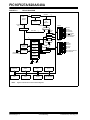
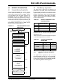
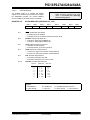
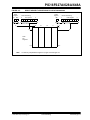
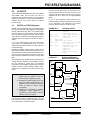
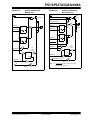
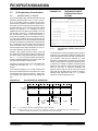
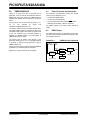
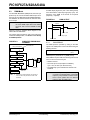
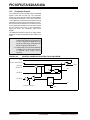
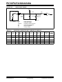
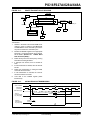
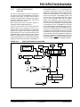
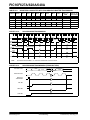
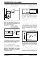
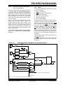
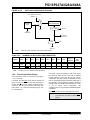
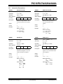
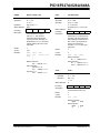
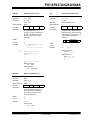
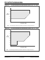
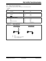
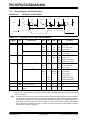
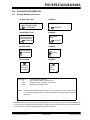
PIC16F627A/628A/648A 10.5 Comparator Outputs The comparator outputs are read through the CMCON register. These bits are read only. The comparator outputs may also be directly output to the RA3 and RA4 I/O pins. When the CM<2:0> = 110 or 001, multiplexors in the output path of the RA3 and RA4/T0CK1 pins will switch and the output of each pin will be the unsynchronized output of the comparator. The uncertainty of each of the comparators is related to the input offset voltage and the response time given in the specifications. Figure 10-3 shows the comparator output block diagram. The TRISA bits will still function as an output enable/ disable for the RA3 and RA4/T0CK1 pins while in this mode. Note 1: When reading the PORT register, all pins configured as analog inputs will read as a ‘0’. Pins configured as digital inputs will convert an analog input, according to the Schmitt Trigger input specification. 2: Analog levels on any pin that is defined as a digital input may cause the input buffer to consume more current than is specified. FIGURE 10-3: MODIFIED COMPARATOR OUTPUT BLOCK DIAGRAM CnINV To RA3 or RA4/T0CK1 pin CnVOUT To Data Bus CMCON<7:6> Q D Q3 EN RD CMCON Q Set CMIF bit D EN CL Q1 From other Comparator Reset DS40044B-page 64 Preliminary 2004 Microchip Technology Inc.