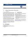
1
PSoC CY8C20x34 TRM
PSoC® CY8C29x66,
CY8C27x43, CY8C27x43E,
CY8C21x34
LIN Bus 2.0
PSoC Reference Design. Revision **
Cypress Semiconductor
198 Champion Court
San Jose, CA 95134-1709
Phone (USA): 800.858.1810
Phone (Intnl.): 408.943.2600
http://www.cypress.com
Copyrights
Copyrights
Copyright © 2006 Cypress Semiconductor Corporation. All rights reserved.
Cypress, the Cypress logo, and PSoC® are registered trademarks and PSoC Designer™, Programmable System-on-Chip™,
and PSoC Express™ are trademarks of Cypress Semiconductor Corporation (Cypress). All other trademarks or registered
trademarks referenced herein are the property of their respective owners.
The information in this document is subject to change without notice and should not be construed as a commitment by
Cypress. While reasonable precautions have been taken, Cypress assumes no responsibility for any errors that may appear
in this document. No part of this document may be copied or reproduced in any form or by any means without the prior written
consent of Cypress. Made in the U.S.A.
Disclaimer
CYPRESS MAKES NO WARRANTY OF ANY KIND, EXPRESS OR IMPLIED, WITH REGARD TO THIS MATERIAL,
INCLUDING, BUT NOT LIMITED TO, THE IMPLIED WARRANTIES OF MERCHANTABILITY AND FITNESS FOR A PARTICULAR PURPOSE. Cypress reserves the right to make changes without further notice to the materials described herein.
Cypress does not assume any liability arising out of the application or use of any product or circuit described herein. Cypress
does not authorize its products for use as critical components in life-support systems where a malfunction or failure may reasonably be expected to result in significant injury to the user. The inclusion of Cypress’ product in a life-support systems application implies that the manufacturer assumes all risk of such use and in doing so indemnifies Cypress against all charges.
Flash Code Protection
Note the following details of the Flash code protection features on Cypress devices.
Cypress products meet the specifications contained in their particular Cypress Data Sheets. Cypress believes that its family of
products is one of the most secure families of its kind on the market today, regardless of how they are used. There may be
methods, unknown to Cypress, that can breach the code protection features. Any of these methods, to our knowledge, would
be dishonest and possibly illegal. Neither Cypress nor any other semiconductor manufacturer can guarantee the security of
their code. Code protection does not mean that we are guaranteeing the product as "unbreakable."
Cypress is willing to work with the customer who is concerned about the integrity of their code. Code protection is constantly
evolving. We at Cypress are committed to continuously improving the code protection features of our products.
2
PSoC Reference Design. Revision **
Contents
1.1 LIN Bus 2.0 Demonstration Kit Description .......................................................................................5
1.1.1
Introduction ..............................................................................................................5
1.2
Kit Contents ...............................................................................................................................5
1.3
Getting Started ...........................................................................................................................5
1.4
LIN Bus Demonstration ..............................................................................................................6
1.5
Master Node Port Pin Usage .....................................................................................................9
1.6
Slave 1 Port Pin Usage ..............................................................................................................9
1.7
Slave 2 Port Pin Usage ............................................................................................................10
1.8
Design IP .................................................................................................................................10
1.9
Demonstration Projects............................................................................................................10
1.10
Other Features .........................................................................................................................10
1.11
Support ....................................................................................................................................10
2.1 System Architecture Overview ..........................................................................................................11
2.2
Features of the PSoC LIN Bus 2.0 Design...............................................................................11
2.3
LIN Frame ................................................................................................................................11
2.3.1
Basic LIN Frame ...................................................................................................11
2.3.2
Break Field.............................................................................................................12
2.3.3
Synch Byte.............................................................................................................12
2.3.4
Protected Identifier.................................................................................................12
2.3.5
Data .......................................................................................................................12
2.3.6
Checksum ..............................................................................................................12
2.3.7
Frame Transfers on the LIN Bus............................................................................12
2.4
Hardware Architecture .............................................................................................................13
2.4.1
LIN Transceiver .....................................................................................................13
2.4.2
Voltage Regulator .................................................................................................13
2.4.3
External Pin Connections ......................................................................................13
3.1 Master Software Architecture ............................................................................................................15
3.1.1
Overview ................................................................................................................15
3.1.2
Foreground Processing..........................................................................................15
3.1.3
Timing and Interrupts .............................................................................................16
3.2
Device Configurations ..............................................................................................................16
3.2.1
Synchro Break Configuration .................................................................................16
3.2.2
Data Transmission Configuration...........................................................................16
3.2.3
Data Reception Configuration................................................................................16
3.3
Firmware ..................................................................................................................................17
3.3.1
Overview ................................................................................................................17
3.3.2
Synchro Break Interrupt .........................................................................................17
3.3.3
TX Interrupt ............................................................................................................17
3.3.4
RX Interrupt............................................................................................................17
3.3.5
Bit Time Interrupt ...................................................................................................17
3.3.5.1
Synchro Break Configuration ..............................................................17
3.3.5.2
Data Transmission Configuration .......................................................17
3.3.5.3
Data Reception Configuration .............................................................18
LIN Bus 2.0 Reference Design
1
Contents
3.4
3.5
3.6
Source Code Files ................................................................................................................... 18
Header Files ............................................................................................................................ 18
Creating a Project Using the Design IP ................................................................................... 18
3.6.1
Importing the Design ............................................................................................. 18
3.6.2
Configuring Global Resources............................................................................... 19
3.6.3
Configuring GPIO .................................................................................................. 19
3.6.4
Routing the Signals ............................................................................................... 19
3.6.5
Setting the Baud Rate ........................................................................................... 20
3.6.6
Adding the Schedule Timer ................................................................................... 20
3.6.7
Setting the Source Clock and Period .................................................................... 20
3.6.8
Configuring the Signal Table.................................................................................. 20
3.6.9
RAM Allocation ...................................................................................................... 20
3.6.10
Frame Definition .................................................................................................... 20
3.6.11
Schedule Table ...................................................................................................... 22
3.6.11.1 Structure of Schedule Table ................................................................ 22
3.6.11.2 An Example Schedule Table ............................................................... 22
3.6.11.3 Diagnostic Schedules .......................................................................... 23
3.6.12
Adding the Main Application .................................................................................. 23
3.6.13
Special Features .................................................................................................... 23
3.6.13.1 Low Power Management..................................................................... 23
3.6.13.2 Node Configuration.............................................................................. 24
3.6.13.3 Implementation of Sporadic Frames....................................................24
3.7
Master Design APIs ................................................................................................................. 25
3.7.1
Basic Functions ..................................................................................................... 25
3.7.2
Miscellaneous Core API Functions........................................................................ 26
3.7.3
LIN Node Configuration API Functions.................................................................. 27
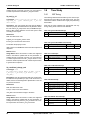
3.8
Time Study............................................................................................................................... 28
3.8.1
ISR Timing ............................................................................................................. 28
3.8.2
Calculation of CPU Overhead Over a Frame ........................................................ 29
3.8.3
Maximum Interrupt Latency ................................................................................... 29
4.1 Slave Software Architecture .............................................................................................................. 31
4.1.1
Overview................................................................................................................ 31
4.1.2
Foreground Processing ......................................................................................... 31
4.1.3
Timing and Interrupts ............................................................................................. 31
4.2
Device Configuration ............................................................................................................... 32
4.2.1
Synchro Reception Configuration .......................................................................... 32
4.2.2
Data Reception Configuration................................................................................ 32
4.3
Firmware.................................................................................................................................. 32
4.3.1
Overview................................................................................................................ 32
4.3.2
GPIO Interrupt ....................................................................................................... 32
4.3.3
Synchro Timer Interrupt ......................................................................................... 33
4.3.4
Synchro Timeout Interrupt ..................................................................................... 33
4.3.5
RX Interrupt ...........................................................................................................33
4.3.6
TX Interrupt............................................................................................................ 34
4.3.7
Bit Timer Interrupt ................................................................................................. 34
4.4
LIN Source Code Files............................................................................................................. 34
4.5
Header Files ............................................................................................................................ 34
4.6
Using the Design IP ................................................................................................................. 35
4.6.1
Importing the Design ............................................................................................. 35
4.6.2
Configuring Global Resources............................................................................... 35
4.6.3
Configuring GPIO .................................................................................................. 35
4.6.4
Routing the Signals ............................................................................................... 36
4.6.5
Configuring the Signal Table.................................................................................. 36
2
LIN Bus 2.0 Reference Design
Contents
4.6.5.1
RAM Allocation ....................................................................................36
Frame Definition.....................................................................................................37
Response_Error Bit Definition................................................................................37
Node Information ...................................................................................................37
Adding the Main Application ..................................................................................37
Special Features ....................................................................................................38
4.6.10.1 Power Management.............................................................................38
4.6.10.2 Node Configuration..............................................................................38
4.6.10.3 Implementing Event-Triggered Frames ...............................................38
4.7
LIN 2.0 Slave Design API ........................................................................................................39
4.8
Time Study ...............................................................................................................................40
4.8.1
ISR and Function Timing .......................................................................................40
4.8.2
Calculation of CPU Overhead Over a Frame.........................................................41
4.8.3
Maximum Interrupt Latency ...................................................................................41
5.1 Demonstration Projects Introduction ...............................................................................................43
5.2
LIN Description File (LDF)........................................................................................................43
5.2.1
Description .............................................................................................................43
5.2.2
Example LDF .........................................................................................................44
5.3
Example Project for Master (CEM) ..........................................................................................47
5.3.1
Description .............................................................................................................47
5.3.2
Example Master Program ......................................................................................47
5.4
Example Project for Slave 1 (CPM) .........................................................................................52
5.4.1
Description .............................................................................................................52
5.4.2
Example Slave 1 Program .....................................................................................52
5.5
Example Project for Slave 2 (DIA) ...........................................................................................54
5.5.1
Description .............................................................................................................54
5.5.2
Example Slave 2 Program .....................................................................................54
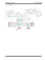
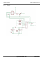
6.1 Board Schematics ..............................................................................................................................57
6.1.1
Power Supply.........................................................................................................57
6.1.2
Master ....................................................................................................................58
6.1.3
Slave 1 ...................................................................................................................59
6.1.4
Slave 2 ...................................................................................................................60
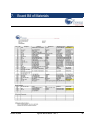
7.1 Board Bill of Materials .......................................................................................................................61
4.6.6
4.6.7
4.6.8
4.6.9
4.6.10
LIN Bus 2.0 Reference Design
3
Contents
4
LIN Bus 2.0 Reference Design
1.
LIN Bus 2.0 Kit
1.1
LIN Bus 2.0 Demonstration Kit Description
1.1.1
Introduction
The LIN Bus Demonstration Kit demonstrates the ability of
the PSoC® Programmable System-on-Chip™ to implement
LIN bus, Local Interconnect Network, standard protocol. The
LIN bus was developed to fill the need for a low cost automotive network to complement existing networks. LIN bus
also finds many uses in non-automotive distributed systems
where a robust, low-speed and low-cost protocol is required.
Additional information is located on the LIN consortium web
site at http://www.lin-subbus.org where you can also find the
complete LIN specifications for version 2.0.
This design provides a flexible development environment for
creation of either slave or master LIN device applications
using the PSoC. The demonstration board has one master
and two slave nodes. Using dynamic reconfiguration, hardware resources are minimized with low CPU overhead.
Design details on specific implementation provided with the
demonstration board are included in the supplied Lin Master
Node Design IP, Lin Slave Design IP, Application Note
AN2045, and in the corresponding project comments inside
PSoC Designer™.
1.2
■
■
■
■
1.3
Getting Started
The LIN bus demonstration board is preprogrammed to
demonstrate the LIN bus directly out of the box. To demonstrate functionality, follow these steps:
1. Verify contents in design kit.
2. Plug the power supply into a wall outlet (international
plug adaptors are included). The power supply automatically adapts to this voltage and frequency range: 100240 VAC at 50-60 Hz.
3. Connect the barrel plug of the power supply cord into the
demonstration board. The green power LED next to the
power jack lights.
The demonstration board is now fully operational and demonstrates LIN bus operations. Functional details of the
examples running on the board can be found in section 1.4,
LIN Bus Demonstration, on page 6.
Kit Contents
LIN Bus Demonstration Board
International Power Supply (110-220 VAC to 12V DC)
Serial Cable (DB-9)
Software CD with Documentation, Example Project, and
Design IP
October 25, 2006
Cypress Semiconductor – Rev. **
5
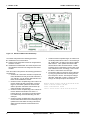
1. LIN Bus 2.0 Kit
LIN Bus 2.0 Reference Design
Power
Jack
Power
Supply
Master
Serial Port
Master
Node
Slave
1
Prototype
Area
Slave
2
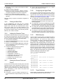
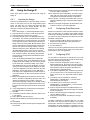
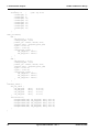
Figure 1-1. LIN Bus Demonstration Board
The master node and slave 1 are both implemented in a 28pin part, CY8C27443-24PXI. Slave 2 is implemented in an
8-pin part, CY8C27143-24PXI.
The CD-ROM that is included with this kit has all project files
for the designed-in devices as well as project files for automotive grade devices.
1.4
LIN Bus Demonstration
The LIN bus demonstration board is divided into four
regions: master node, slave 1, slave 2, and the prototype
area.
The master node has a bank of 8 dip-switches, SW2, and a
bank of 10 LEDs, U8. Slave 1 also has a set of 8 dipswitches, SW1, and a bank of 10 LEDs, U7. Slave 2 has 2
push-button switches, S1 and S2, and 2 individual green
LEDs, D2 and D4. Figure 1-1 shows the positions of these
components.
6
Cypress Semiconductor – Rev. **
October 25, 2006
LIN Bus 2.0 Reference Design
1. LIN Bus 2.0 Kit
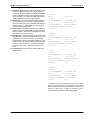
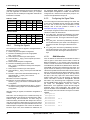
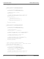
U8
SW2
U7
SW1
S2
S1
D2 D4
Figure 1-2. Layout of Node-Specific Switches and LEDs
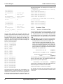
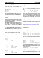
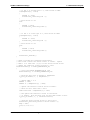
Periodically, the master node sends its switch state information to slave 1 and then polls both slaves for their switch
state information. In response, the master and slaves display the state of the information as specified by the switchto-display relationship. Figure 1-3 and the following list show
the switches and the LEDs that they control:
■ Master node dip-switches 8 to 1 control slave 1’s LEDs 1
to 8. Note that the dip-switch numbering is reversed but
is oriented such that the left most switch, numbered 8,
controls the left most LED of slave 1.
■ Slave 1’s dip-switches 8 to 5 control master node LEDs
1 to 4.
■ Slave 1 measures the resistance connected between
P0[1] and P0[3] and sends this information to the master.
To make the resistance measurement, a reference resistance of 2.2K is connected between P0[1] and P0[2].
These resistance connections can be made to the
header (SV3) meant for port 0 of slave 1.
■ Slave 1’s dip-switches 2 and 1 control slave 2 LEDs, D2
and D4. These switches are configured to implement a
left / right turn indicator. When one of these switches is
closed, D2 or D4 blinks.
■ Slave 2’s push-button switches, S2 and S1, control master node LEDs 5 and 6.
October 25, 2006
■
The remaining switches and LEDs are not used, but
board connections are provided for use in the prototype
area.
Cypress Semiconductor – Rev. **
7
1. LIN Bus 2.0 Kit
LIN Bus 2.0 Reference Design
Figure 1-3. Switch-to-LED Control Relationship
The master node performs the following operations.
■ Initializes the LIN communication.
■ Calls the node configuration function to configure slave 1
and slave 2 nodes.
■ Initializes the Schedule table. The frame sequence and
time allotted for each frame is configured in the Schedule table.
Then the master node performs the following operations in
an infinite loop:
❐ Checks if the current frame transfer is complete and
if the LIN hardware is ready to send the next frame. If
yes, calls the l_sch_tick function that loads the next
frame due and initiates the transfer.
❐ Checks if Frame1 completion flag is set. Frame1 carries the master's dip-switch information. If Frame1
flag is set, the master updates the Frame1 buffer
with the dip-switch information and sends the dipswitch information over serial port.
❐ Checks if Frame2 completion flag is set. Frame2 carries the resistance information from slave 1. If
Frame2 flag is set, converts the 2-byte HEX integer
to an ASCII string and sends this string over the
serial port.
❐ Checks if Frame3 completion flag is set. Frame3 carries the switch status of slave 2. If Frame3 flag is set,
updates LED 5 and LED 6 according to the switch
status and sends the Slave-2 switch status over
serial port.
8
❐
❐
Checks if Frame4 completion flag is set. Frame4 carries the dip-switch status of slave 1. If Frame4 flag is
set, updates LED 1 to LED 4 as per status of SW8 to
SW5 of slave 1. Then updates the Frame5 buffer
with the status of SW1 and SW2 of slave 1. When
Frame5 is due, this information is sent to slave 2 and
slave 2 blinks D4 or D5, accordingly. Then it sends
the Slave-1 switch status over serial port.
The master's data over serial port may be observed
by using a HyperTerminal and connecting the master's serial port to the PC. The serial port setting is
38.4 kbps, 8 data bits, no parity, 1 stop bit. The following is an example output on the serial port:
Master Switch Status: ON ON ON ON ON ON ON ON
Slave 2 Switch Status: ON OFF
Slave 1 Resistance: 25000
Slave 1 Switch Status: ON ON ON ON ON ON ON ON
Cypress Semiconductor – Rev. **
October 25, 2006
LIN Bus 2.0 Reference Design
1.5
1. LIN Bus 2.0 Kit
Master Node Port Pin Usage
1.6
Slave 1 Port Pin Usage
The pin usage for the LIN bus PSoC master node is as follows:
The section details the pin usage for the LIN bus PSoC
slave 1:
Table 1-1. Port 0 – Pins Connect to User-Accessible
Header Row
Table 1-4. Port 0 – Pins Connect to User-Accessible
Header Row
0
Not used
0
Not used
1
Not used
1
2
Not used
Common point of measured resistance and reference
resistance
3
Not used
2
Reference resistance
4
Not used
3
Measured resistance
LIN bus RX
4
LIN bus TX
LIN bus TX
5
LIN bus RX
6
UART RX
6
Not used
7
UART TX
7
Not used
5
4
Table 1-2. Port 1 – Pins Connect to User-Accessible
Header Row and LEDs
Table 1-5. Port 1 – Pins Connect to User-Accessible
Header Row and LEDs
Crystal out
0
LED controlled by master, Port2_0 switch
Crystal in
1
LED controlled by master, Port2_1 switch
2
LED controlled by slave 2, Port0_7 switch
2
LED controlled by master, Port2_2 switch
3
LED controlled by slave 2, Port0_2 switch
3
LED controlled by master, Port2_3 switch
4
LED controlled by master, Port2_4 switch
5
LED controlled by master, Port2_5 switch
6
LED controlled by master, Port2_6 switch
7
LED controlled by master, Port2_7 switch
0
1
4
5
LED controlled by slave 1, Port2_4 switch
LED controlled by slave 1, Port2_5 switch
6
LED controlled by slave 1, Port2_6 switch
7
LED controlled by slave 1, Port2_7 switch
Table 1-3. Port 2 – Pins Connect to User-Accessible
Header Row and Dip-Switches
0
1
Switch controls slave 1, Port1_0 LED
Switch controls slave 1, Port1_1 LED
2
Switch controls slave 1, Port1_2 LED
3
Switch controls slave 1, Port1_3 LED
4
5
Switch controls slave 1, Port1_4 LED
Switch controls slave 1, Port1_5 LED
6
Switch controls slave 1, Port1_6 LED
7
Switch controls slave 1, Port1_7 LED
October 25, 2006
Table 1-6. Port 2 - Pins Connect to User-Accessible
Header Row and Dip-Switches
0
Switch not used
1
Switch not used
2
Switch controls slave 2, Port1_1 LED blinking control
3
Switch controls slave 2, Port1_0 LED blinking control
4
Switch controls master, Port1_4 LED
5
Switch controls master, Port1_5 LED
6
Switch controls master, Port1_6 LED
7
Switch controls master, Port1_7 LED
Cypress Semiconductor – Rev. **
9
1. LIN Bus 2.0 Kit
1.7
LIN Bus 2.0 Reference Design
Slave 2 Port Pin Usage
The section details the pin usage for the LIN bus PSoC
slave 2:
Table 1-7. Port 0 – Pins
2
Push button controls master, Port1_3 LED
4
LIN bus TX
5
LIN bus RX
7
Push button controls master, Port1_2 LED
Table 1-8. Port 1 – Pins
0
Blinking LED controlled by slave 1, Port2_3 switch
1
Blinking LED controlled by slave 1, Port2_2 switch
1.8
1.10
Other Features
In addition to the three LIN nodes, the demonstration board
provides several other features:
■ Unregulated 12V DC 500 mA power supply for prototype
use.
■ Regulated 5V DC 500 mA power supply for prototype
use.
■ U12 header provides access to LIN bus for probing or
bus extension.
■ Disconnectable LIN nodes from the LIN bus by removing
the JP1, JP2, or JP3 jumpers.
■ Prototype area provides power and ground connections,
and two strips of holes for prototyping. The holes are
connected in rows of three to simplify connections, and if
required, the traces can be cut.
5V
5V
Design IP
LIN Master Node and LIN Slave Node Design IP are provided on the CD and on the Cypress Semiconductor web
site at http://www.cypress.com.
Design IP in PSoC Designer allows a user to import the
required solution, precomposed of configurations and software APIs, to quickly and easily implement a LIN bus node.
To import the Design IP into a project, use the PSoC
Designer Design Browser (under Config >> Import Design).
The LIN Master Node Design IP and the LIN Slave Node
Design IP documentation are located in the root directory of
the CD.
1.9
Demonstration Projects
Also included on the CD are the three PSoC projects that
implement the master and slave nodes on the demonstration board delivered with this design kit. The demonstration
projects are in the following directories of the CD:
■ Demonstration Projects\Master Node\MasterLinDemo
■ Demonstration Projects\Slave 1 Node\CLinSlaveDemo
■ Demonstration Projects\Slave 2 Node\CLinSlaveDemo2
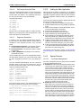
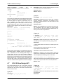
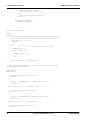
Gnd
Gnd
Figure 1-4. Prototype Area Through Hole Connections
■
■
■
■
■
■
Install header U13 to short LED D2. This allows development of self-diagnostic indicator faults.
Remove jumper JP4 to provide an open circuit at LED
D4. This provides an additional way to develop self-diagnostic indicator faults.
You can emulate master node and slave 1 using a universal emulation pod, from a PSoC Basic Development
Kit, mounted on the standard 28-pin DIP foot.
You can emulate slave 2 using a universal emulation
pod mounted on the standard 8-pin DIP foot.
The four unused LEDs in the master node LED array are
provided on pads LED 0-3 for prototyping.
The two unused LEDs in the slave 1 LED array are provided on pads LED 4-5 for prototyping.
1.11
Support
Support for the PSoC device, the development tools or the
LIN bus demonstration board can be found on our web site
at http://www.cypress.com, http://www.cypress.com/support
or by calling the Applications Hotline at 425.787.4814.
10
Cypress Semiconductor – Rev. **
October 25, 2006
2.
System Architecture
2.1
Overview
The LIN bus, Local Interconnect Network, is an asynchronous, 1 wire, single master, multiple slave network. It is most
commonly used in automobile networks.
■
■
■
2.2
■
■
■
■
■
■
■
Features of the PSoC LIN
Bus 2.0 Design
Single master, multiple slaves - up to 16 slaves.
Message-based protocol.
Single wire - maximum 40 m.
Data rates of 2.4K, 4.8K, 9.6K and 19.2K are supported
by master.
Slaves capable of synchronizing to any baud rate from
2K to 20K.
Self synchronization of slaves to master’s speed.
Data format similar to common serial UART format.
■
■
Safe behavior with data checksums and bit-error detection.
100% LIN Bus 2.0 protocol-compliant.
Master design uses minimal resources (only three digital
blocks) and is easy to implement (using overlapping
configurations).
Slave designs use minimal resources (only four digital
blocks) and are easy to implement (using overlapping
configurations). The slave design for the CY8C21x34
device family uses the least amount of system
resources.
The PSoC design IP is provided for master and slave
nodes in the following device families:
❐ CY8C29x66 Industrial
❐ CY8C27x43 Automotive
❐ CY8C27x43 Industrial
❐ CY8C21x34 Industrial
Figure 2-1. Structure of a LIN Frame
2.3
2.3.1
LIN Frame
It is made of a break field followed by 4 to 11 byte fields.
Each byte field is transmitted as a serial byte as shown in
Figure 2-2.
Basic LIN Frame
The LIN communication takes place in frames. Figure 2-1
shows the structure of a frame.
October 25, 2006
Cypress Semiconductor – Rev. **
11
2. System Architecture
LIN Bus 2.0 Reference Design
Figure 2-2. Structure of a Byte Field
2.3.2
Break Field
■
The break symbol is used to signal the beginning of a new
frame. It is the only field that does not comply with Figure 22. A break is always generated by the master and is at least
13 bits of dominant value, including the start bit, followed by
a break delimiter, as shown in Figure 2-3. The break delimiter is at least one nominal bit-time long. A slave node uses
a break detection threshold of 11 nominal bit times.
■
■
Identifiers 60 (0x3C) and 61 (0x3D) are used for diagnostic frames.
Identifier 62 (0x3E) is used for user-defined extensions.
Identifier 63 (0x3F) is used for future protocol enhancements.
More details on protected identifiers are in the LIN Bus 2.0
specifications at http://www.linsubbus.org.
2.3.5
The protected Identifier is followed by 1 to 8 bytes of data.
The number of data bytes carried by a frame is defined in
the LIN definition file (LDF). This file also defines whether
the data bytes are sent from the master to a slave or from a
slave to the master. Data that are longer than 1 byte are
transmitted LSB first (Little Endian mode).
Figure 2-3. The Break Field
2.3.6
2.3.3
Synch Byte
The synch byte is sent to the slave to synchronize to the
master’s baud rate. The synch byte is nothing but a data
field with 0x55 as data. The synch byte is shown in Figure 34.
Figure 2-4. The Synch Byte
The slave measures the time between the start bit and the
fourth falling edge of the synch byte. Then dividing this by
eight, gives the single bit time. Based upon this time, the
slave sets the clock to its UART so that it can send/receive
the data bytes of the frame at the master’s bit rate.
2.3.4
Protected Identifier
The byte that follows the synch byte is the protected identifier. This byte has two parts. Bits 0-5 form the actual identifier (0 to 63). Bits 6 and 7 form the identifier parity. The
identifiers can be split into four different categories:
■ Identifiers 0 - 59 are used for signal-carrying frames.
12
Data
Checksum
The last field of a frame is the checksum. The checksum
contains the inverted 8-bit sum with carry over all data bytes
or all data bytes and the protected identifier. Checksum calculation over only the data bytes is called classic checksum
and is used for communication with LIN bus 1.x slaves.
Checksum calculation over both the data bytes and the protected identifier byte is called enhanced checksum and it is
used for communication with LIN bus 2.0 slaves. The checksum is transmitted in a byte field. Use of classic or
enhanced checksum is managed by the master node and
determined per frame identifier; classic in communication
with LIN bus 1.x slave nodes and enhanced in communication with LIN bus 2.0 slave nodes. Identifiers 60 (0x3c) to 63
(0x3f) always use classic checksum.
The complete LIN standard is available at http://www.linsubbus.org.
2.3.7
Frame Transfers on the LIN Bus
Only the master initiates a frame. The master allocates a
time slot for each frame. The master also sends the frames
in a predetermined sequence. The information sequence of
the frames and the time slot for each frame is available in a
table called Schedule table. Each entry of this table
describes the protected identifier of the frame to be initiated
and also the time to be allotted for that frame. When all the
Cypress Semiconductor – Rev. **
October 25, 2006
LIN Bus 2.0 Reference Design
2. System Architecture
frames in the Schedule table have been transmitted, the
next cycle starts again from the first frame of the table.
The LIN 2.0 API has many functions to manage the Schedule table. It has functions to select tables, to initiate the
transfer of the next frame in the current table, and so on.
More details on these APIs are found in section 3, Master
Design APIs, on page 25.
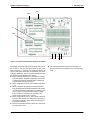
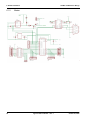
Figure 2-5. Hardware Configuration of a LIN Master/Slave
2.4
Hardware Architecture
Figure 2-5 shows the hardware architecture for the LIN Master/Slave.
2.4.1
LIN Transceiver
Because the physical LIN bus is held at Vbat in the range of
8 to 18 volts, a LIN transceiver device is required to connect
the LIN bus with the PSoC chip. The LIN transceiver converts the single wire LIN bus at 8V – 18 volts to TTL-level TX
and RX signals, which can be connected to the PSoC.
2.4.2
Voltage Regulator
You must use a voltage regulator to provide the PSoC Vcc
supply. LIN transceivers with built-in regulators are available.
2.4.3
External Pin Connections
You have the option to decide which pins to use for the TX
and RX pins in the design. These connections are done in
the Device Editor of PSoC Designer. Details on how to configure the pins are in section 5, Using the Design IP, on
page 35.
October 25, 2006
Cypress Semiconductor – Rev. **
13
2. System Architecture
14
LIN Bus 2.0 Reference Design
Cypress Semiconductor – Rev. **
October 25, 2006
3.
Master Design IP
3.1
Software Architecture
3.1.1
Overview
The software architecture maximizes interrupt processing to
minimize the processing overhead on the end application.
All message processing through configurations is performed
at the interrupt level. Each stage is designed as a state
machine and, upon completion, this state machine unloads
itself and loads in the next required configuration to propagate the message to completion through the LIN message
protocol sequence. Each message scheduled for processing is identified by the identifier byte in the header. The identifier is defined by the agreed master-slave relationship in
the LIN description file (LDF). See the example LDF in section 5, LIN Description File (LDF) on page 43.
The master has a Schedule table where the frames are
defined in the sequence in which they are transmitted on the
bus. This table also contains an entry for the duration slot for
each frame. In addition to the Schedule table, there is a Signal table in which the frames that are used in the system are
defined. This table contains parameters such as the protected identifier, transfer type, checksum mode, data count,
and the pointer to the frame buffer.
There are three transfer types:
■ MASTER_TO_SLAVE where the master sends the data
after the protected ID for the slave to process.
■ SLAVE_TO_MASTER where the slave responds with
data to the master’s request.
■ SLAVE_TO_SLAVE where the master initiates a frame
and the data is transferred from one slave to another.
When a MASTER_TO_SLAVE transaction takes place, the
master transmits the content of the frame’s buffer to the
slave. For SLAVE_TO_MASTER, the master receives the
slave’s response and deposits the data in the frame’s buffer.
For a SLAVE_TO_SLAVE transfer, the master discards all
the data received at the end of the frame.
There are two types of checksum modes used, classic and
enhanced. For LIN 1.x slave nodes, use the classic checksum for all frames. For LIN 2.0 slave nodes, use enhanced
checksum for frames with identifiers 1 through 59. For identifiers 60 to 63, use classic checksum. While creating the
Signal table, refer to the LDF to determine the slave version
before deciding the checksum type.
LIN Bus 2.0 Reference Design, Rev. **
The data count also depends upon the slave type. For
LIN1.x slaves, the data count is fixed for different protected
identifiers. For these frames, the data count is set to zero in
the Signal table. When the master comes across a zero for
data count in this table, it assumes that the default data
count is used and extracts the data count from the protected
identifier. For LIN 2.0 slaves, the data count can be from one
to eight. So the data count entry can have any value from
one to eight. Again, this value must be configured after
studying the LDF.
The buffer pointer is an entry that has the address of the
buffer for the particular frame. The master reads from or
writes to the corresponding frame buffer using the buffer
pointer parameter.
3.1.2
Foreground Processing
The main process must initialize the LIN function and then
set the Schedule table using the l_sch_set function. After
this, the main process performs the actual application. The
successive frame transfers are initiated either inside the
main loop or inside the schedule timer’s interrupt service
routine (ISR). The schedule timer is configured to generate
an interrupt based upon the time base defined in the LDF.
When a frame is read from the Schedule table, the time for
the frame is also read and a loop counter is updated with
this time count. This counter is decremented inside the
schedule timer ISR. When it reaches zero, a flag is set to
indicate that the next frame is ready for processing. The
main function continuously checks this using the
LinMaster_fIsLinReady function. When this flag is set, the
main function calls the l_sch_tick function to start the next
message. Alternatively, the l_sch_tick function can be called
from the schedule timer ISR.
The main program is able to perform other functions inside
the main loop. It checks the status of each frame transfer by
checking the first byte of the frame buffer. It can also update
frames or process received data.
More details on the l_sch_tick function are in the API section
ahead.
15
3. Master Design IP
3.1.3
LIN Bus 2.0 Reference Design
Timing and Interrupts
Automotive applications are often real-time driven. As a
result, the LIN driver only uses interrupts with no active loop
or blocking functions. Overhead measurements made on a
LIN bus with messages transferred at 19200 bauds and the
PSoC CPU running at 24 MHz, show a 0% overhead
between messages, and a maximum of 5% overhead while
sending or receiving messages. Refer to Time Study on
page 28 in this chapter.
3.2
Device Configurations
The LIN master design uses dynamic reconfiguration and
has three configurations, the Synchro Break Configuration,
Data Transmission Configuration and the Data Reception
Configuration. The Synchro Break Configuration generates
the break field. The Data Transmission Configuration sends
the synchronization byte and any data bytes to be transmitted followed by the checksum byte. The Data Reception
Configuration receives the slave’s response data.
3.2.1
the TX8 block’s clock input. When break field generation is
complete, the Data Transmission Configuration is loaded
and 0x55 is transmitted as the synch byte. Next, the protected identifier is transmitted. The protected identifier is followed by master’s data and the checksum if the frame is
MASTER_TO_SLAVE. Also during the data transmission,
the Bit_time_counter generates an interrupt every bit time.
Inside the Bit_time_counter’s ISR, the TX and RX pins are
compared. If they are not equal, then the BIT_ERROR flag
is set and transmission of the current frame is aborted.
Synchro Break Configuration
Figure 3-1 shows the module placement for the Synchro
Break Configuration. This configuration has one 8-bit
counter (SB_Baud_Rate_Counter) that generates the baud
clock. The output frequency of this clock generator is eight
times the baud rate. There is a second 8-bit counter
(SB_Bit_time_counter) that is used to generate an interrupt
every bit time. Finally, there is a third 8-bit counter
(Synchro_Break_Counter) that generates the actual break
field.
The
period
and
compare
values
of
Synchro_Break_Counter are set in such a way that one full
cycle of the counter produces a break time approximately
equal to 13 bit times and the break delimiter equal to one bit
time. The TX and RX pins are compared to detect any bit
error inside the Bit_time_counter ISR.
Figure 3-2. Data Transmission Configuration
3.2.3
Data Reception Configuration
Figure 3-3 shows the user module placement for the Data
Reception Configuration. This has one 8-bit counter that
generates the baud rate (DR_Baud_rate_counter), one 8-bit
counter that is used to generate interrupts every five bit
times for detecting the slave non-response timeout
(DR_Bit_time_counter), and one RX8 User Module that
receives data (RX8). The DR_Baud_rate_counter is configured to generate a clock eight times that of the baud clock
and feed the RX8 block’s clock input. The received bytes
are transferred to the temporary buffer inside the RX8 ISR.
When all the bytes indicated by the variable bNbDataToReceive have been received, the master processes the
received data. Also, the bit time counter generates an interrupt every five bit times and a timeout counter is decremented inside the DT_Bit_time_counter ISR. The timeout is
set as number of bit times according to the length of the
frame. If the frame is not completed within this timeout (if the
concerned slave stops transmitting), the Synchro Break
Configuration is loaded and the “Slave Not Responding”
error flag is set.
Figure 3-1. Synchro Break Configuration
3.2.2
Data Transmission Configuration
Figure 3-2 shows the user module placement for the Data
Transmission Configuration. This configuration has one 8-bit
counter
that
generates
the
baud
rate
(DT_Baud_rate_counter), one 8-bit counter that is used to
generate interrupts every bit time for detecting bit errors
(DT_Bit_time_counter), and one TX8 User Module to transmit data (TX8). The baud rate generator is configured to
generate a clock eight times that of the baud clock and feed
16
Figure 3-3. Data Reception Configuration
Cypress Semiconductor – Rev. **
October 25, 2006
LIN Bus 2.0 Reference Design
3.3
3.3.1
3. Master Design IP
Firmware
3.3.4
Overview
The initiation of a frame is done by the l_sch_tick function.
This function first reads the Schedule table and loads the
frame parameters of the frame to transmit. It then loads the
Synchro Break Configuration and starts the synchro break
timer. This timer is configured to generate a dominant state
of 13 bit times and a recessive (logic high level on the bus)
state of one bit time. On the terminal count interrupt of this
timer, the Data Transmission Configuration is loaded and
the synch byte of 0x55 is transmitted. The protected identifier
is
transmitted
next.
If
the
transfer
is
MASTER_TO_SLAVE, all data bytes are transmitted one by
one with the checksum as the last byte. If the transfer type is
not MASTER_TO_SLAVE, then the Data Reception Configuration is loaded and the response from the slave is
received. Data is processed after all bytes are received.
Once the l_sch_tick function loads the Synchro Break Configuration and starts the synchro break timer, the rest of the
frame is processed in the background, inside ISRs. More
about the ISRs will be explained in the following sections.
This enables the main function to run in the foreground.
There are four different interrupts processed inside the LIN
master. One or more of these interrupts may be active
depending upon the active state. The code inside each of
these ISRs is well commented so that it is very easy to
understand the operation.
3.3.2
Synchro Break Interrupt
3.3.3
TX Interrupt
3.3.5
Bit Time Interrupt
The bit time interrupt is used in all the configurations.
Synchro Break Configuration
In the Synchro Break Configuration, the bit time counter
generates an interrupt every bit time. Inside the ISR, the TX
and RX pins are compared to check if there is a bit error. If a
bit error is found, the frame is aborted and the Synchro
Break Configuration is reloaded. Also, when the TX state is
sensed as logic high, the TX pin is disconnected from the
global bus and made StdCPU and the TX pin’s state is made
logic high. This is done to prevent the counter output from
becoming logic low upon terminal count before it is stopped
inside the synchro break ISR. This unwanted low transition
could be taken as the falling edge of the synch byte by the
slaves connected to the cluster and may lead to communication errors.
3.3.5.2
Inside the TX ISR, the program checks if this is the first
interrupt. If this is the first interrupt, 0x55 was placed in the
TX shift register and the buffer is empty. The bit time counter
is started and its interrupt enabled. This counter’s interrupt is
used to check for bit errors. The bNbDataToSend variable is
then checked. If this variable equals zero, no more bytes are
sent and the bfLAST_BYTE_SENT flag is set. The completion of the frame takes place inside the Bit_time_counter’s
ISR. If the bNbDataToSend is not zero, then the next byte
sent is transferred to the TX buffer. Then the bNbDataToSend variable is decremented by one before exiting the
ISR.
October 25, 2006
If a response is expected from the slave, the Data Reception
Configuration is loaded. This is done inside the
Bit_time_counter’s ISR for the Data Transmission Configuration. When a byte is received from the slave, this interrupt
is generated. Inside the interrupt, the received data is placed
on a buffer in the RAM. The bNbDataToReceive variable is
decremented and checked if zero. If it is not zero, the ISR is
exited. If this value becomes zero, it means that all the bytes
were received and the Synchro Break Configuration is
loaded to allow for the next frame initiation. Then the
bfDATA_TO_COPY flag is checked. This flag is set if this is
a SLAVE_TO_MASTER transaction and is not set if this is a
SLAVE_TO_SLAVE transaction. For a SLAVE_TO_SLAVE
transaction, the master has nothing to do with the received
data so the data is discarded. For a SLAVE_TO_MASTER
transaction, the checksum of the received data is verified. If
the checksum is valid, the received data is transferred to the
corresponding frame buffer. The checksum of the data bytes
is compared with the last byte of the frame, which is the
checksum transmitted by the slave. If they are identical, the
data is valid. If the data is a slave’s response to a master’s
diagnostics request, the received data is processed for the
RSID, error code etc. of the slave response. Details of RSID
may be found in the LIN 2.0 specifications.
3.3.5.1
The l_sch_tick function loads the Synchro Break Configuration and starts the synchro break counter. The synch
counter clock is from the baud rate clock generator, which
runs at eight times the bit rate. The period of the synch
counter is set to 111. This is equal to 14 bit times. The compare value of the counter is set to eight, which is equal to
one bit time. So the output of the counter remains low for 13
bit times and high for one bit time. At the terminal count, the
synchro break counter generates an interrupt. The Data
Transmission Configuration is loaded inside this ISR. 0x55
is then placed on the TX buffer to generate the synch field.
The rest of the frame is continued from the TX interrupt.
RX Interrupt
Data Transmission Configuration
In the Data Transmission Configuration, the bit time interrupt
is used to compare the TX and RX pins. The number of bits
compared is tracked by the bNbBitsAnalyzed variable. This
variable is initially set to 10, including the start and stop bits
of a byte. Whenever this variable becomes zero, a byte is
analyzed and the bfLAST_BYTE_TRANSMITTED flag is
checked. If this flag is set, the last byte of the frame was
sent. When this happens, the bNbDataToReceive variable is
checked. If this is zero, then the Synchro Break Configuration is loaded. If this is not zero, then the Data Reception
Configuration is loaded to receive the slave’s response.
Cypress Semiconductor – Rev. **
17
3. Master Design IP
3.3.5.3
LIN Bus 2.0 Reference Design
Data Reception Configuration
In the Data Reception Configuration, the bit time counter is
configured to generate an interrupt every five bit times.
Inside this ISR, a timeout counter is decremented by five.
This timeout counter is initialized by the l_sch_tick function
according to the number of data present in the frame. In a
normal frame transaction, the frame is completed before this
counter becomes zero. However, if the slave stops transmitting in the middle of the frame for any reason, and the timeout counter becomes zero, a timeout is detected, the
SLAVE_NOT_RESPONDING error flag is set and the Synchro Break Configuration is loaded.
3.4
Source Code Files
Lin20CoreAPI.asm: This file has all the functions for the
LIN core API.
Lin20NodeConfiguration.asm: This file has all the functions for the node configuration.
Lin20PhysicalLayer.asm: This file has all the code related
to the proper operation of the LIN firmware. This file has all
the ISRs described in section 3.3, Firmware on page 17.
RamVariables.asm: This file has all RAM variable allocations.
SignalTable.asm: This file has the Message table and the
Protected ID table. This file must be modified according to
the LDF.
ScheduleTable.asm: This file has the Schedule tables used
in the master design. This file must be modified according to
the LDF.
LinPowerManagement.c: This file has the functions that
are required for the go to sleep and wakeup operations of
the LIN master.
NodeConfigUtilities.c: This file has some functions that
can be used for node configuration functions.
3.5
Header Files
Lin20CoreAPI.h: This file has all the function prototypes for
the Lin20CoreAPI.asm file.
Lin20NodeConfiguration.h: This file has all the function
prototypes for the Lin20Nodeconfiguration.asm file.
Lin20Defines.h: This file has the variable types defined in
the LIN specifications.
Lin20Master.h: This file has the definitions of different constants and flags used in the firmware.
LinPowerManagement.h: This file has the function prototypes for the LinPowerManagement.c file.
NodeConfigUtilities.h: This file has the function prototypes
for the NodeConfigUtilities.c file.
18
SignalTable.h: This file has declarations of the signal buffers and frame names used in the SignalTable.asm file.
ScheduleTable.h: This file has the declarations of the
Schedule table names used in the ScheduleTable.asm file.
Lin20Master.inc: This file has the definitions of all the constants and flags used by the Lin20PhysicalLayer.asm file.
Of all source code and header files, you must modify the following files according to the LDF.
■ Lin20Master.inc
■ SignalTable.asm
■ SignalTable.h
■ ScheduleTable.asm
■ ScheduleTable.h
3.6
Creating a Project Using the
Design IP
Follow these steps to create a LIN master PSoC project
using the Design IP.
3.6.1
Importing the Design
There are two ways to import the design. One is to create a
new project in PSoC Designer and use the design-based
project option. The other is to create a project and then
import the design using the Design Browser. The recommended method is to create a new design-based project.
1. Select
File >> New Project >> Create Design-Based Project.
2. Select the directory in which to create the project files.
3. Select the directory and name for a project.
4. The Design Browser opens. The Design Browser has
two windows. The window on the left side is the Design
Browser itself where you select the design. The window
on the right side shows the data sheet for the selected
design. On the top of the Design Browser window there
are two radio buttons that select between “Browse File
System” and “Select From Design Catalog.” Click the
"Browse File System" option. Navigate to the "\Design
IP\Lin2.0 Master" directory on the CD, and open the
folder corresponding to the device that you want to use.
Then select the .cfg file in this directory. Now the data
sheet window on the right shows the data sheet of the
LIN master design.
5. Below the Design Browser window, there are two radio
buttons, “Overwrite configurations with same name” and
“Resolve configuration name conflicts.” Use these
options when importing a design into an already-existing
project and if some of the configurations from the existing project have the same name as that of the imported
design.
6. Below this there are two windows, “Resolve name conflicts” and the “Specify base configuration.” The “Specify
base configuration” window has the Synchro Break Configuration, Data Transmission Configuration and Data
Reception Configurations listed. Do not select any of
these options.
Cypress Semiconductor – Rev. **
October 25, 2006
LIN Bus 2.0 Reference Design
3. Master Design IP
7. The “Resolve name conflicts” window lists functions in
the imported design that have the same name as functions in the existing project. When there is a name conflict, clicking the “Auto Resolve” button automatically
renames the conflicting function names.
8. Below this, details of the design such as date of creation,
description and the base part number are displayed.
9. Click OK.
10. Now in the Device Selection window, select the device
for the project.
11. Select “Generate main file using C.”
12. Select “Device Editor” as the Designer State.
13. Click Finish.
14. A Design Import Status window opens and displays the
import status.
15. When the design is imported, PSoC Designer opens the
Device Editor.
16. Four configurations are visible. The base configuration
with the project name, the Synchro Break Configuration,
Data Transmission Configuration and the Data Reception Configuration.
17. Go to Project >> Settings, Device Editor tab. In the configuration initialization type, select “Direct Write (Speed
Efficient).”
18. Now switch to the base configuration and select all the
user modules to include in the main application.
3.6.2
The GPIO configuration is done. After this, modify the GPIO
of the other port pins according to the main project requirements. Whenever a modification is done in the base configuration, the same settings are updated in the other three
configurations. Thus, regardless of which configuration is
active, the GPIO state of the main application is maintained.
When the process is complete, the configuration of the TX
and RX pins looks like this:
Table 3-1. TX Pin
Configuration
Base
Name
TX
Port
As selected
Drive
Interrupt
GlobalOut Strong
Select
DisableInt
Synchro Break
TX
As selected
GlobalOut Strong
DisableInt
Data Transmission
TX
As selected
GlobalOut Strong
DisableInt
Data Reception
TX
As selected
GlobalOut Strong
DisableInt
Configuring Global Resources
Now switch to the Interconnect View and select the base
configuration. First, configure all the global resources
related to the LIN design. Whatever changes made to the
base configuration, are reflected in the other three loadable
configurations.
1. Set CPU speed to 24 MHz. (Set the CPU speed to 12
MHz for the CY8C27x43 automotive grade device.)
2. Set 32 kHz to External.
3. Set the PLL to Enabled.
4. Set VC1 divider to 12.
These are the required global resources for the LIN master.
The clock VC1 is used as the source clock to LIN modules.
The divider is set to 12 in the firmware so that the output of
VC1 is 2 MHz. Take this into account when using VC1 and
VC2 in the main application. You can set all the other global
resources in your main application.
3.6.3
you plan to use as the TX pin as “TX.” Capitalize these
letters.
4. In the Select column of the RX pin, select the
GlobalInOdd_x or GlobalInEven_x. The drive mode
automatically becomes High Z.
5. In the Select column of the TX pin, select the
GlobalOutOdd_x or GlobalOutEven_x. The drive mode
automatically becomes Strong.
6. Switch to synchro break, data transmission and data
reception configurations and check that these changes
are reflected.
Configuring GPIO
Next, decide the TX and RX pins of the LIN bus. To properly
select their drive modes in all configurations, follow these
steps carefully.
1. Switch to the base configuration. Use the Config >>
Restore default pinout. All the pins in the GPIO configuration pane become StdCPU, High Z Analog, DisableInt.
Repeat this step for the synchro break, data transmission and data reception configurations.
2. Return to the base configuration.
3. In the GPIO configuration pane, rename the port pin you
plan to use as the RX pin to “RX.” Then rename the pin
October 25, 2006
Table 3-2. RX Pin
Configuration
Name
Base
RX
Synchro Break
Port
Select
Drive
Interrupt
As selected
GlobalIn
High Z
DisableInt
RX
As selected
GlobalIn
High Z
DisableInt
Data Transmission RX
As selected
GlobalIn
High Z
DisableInt
Data Reception
As selected
GlobalIn
High Z
DisableInt
3.6.4
RX
Routing the Signals
The next step is to route the signals to the digital blocks of
the LIN configurations.
1. Go to the Synchro Break Configuration.
2. Route the Compare Out of the synchro break counter to
the appropriate Row_1_Output_x line. For example, if
you have configured P0[3] as TX pin, then route the
Compare out to Row_1_Output_3 net.
3. From this Row_1_Output_x net, route the signal to the
appropriate GlobalOut bus to which the TX pin is connected.
4. Switch to the Data Transmission Configuration.
5. Route the output of the TX8 to the same
Row_1_Output_x line used by the synchro break
counter (step 2) and from there to the GlobalOut bus to
which TX pin is connected.
6. Switch to the Data Reception Configuration.
7. Route the Global_Input net to which RX is connected, to
an appropriate Row_1_Input_x net. Select Synch to
SysClk in the Synchronization box. For example, if P0[2]
is used as RX, then connect GlobalIn_Even_2 bus to
Row_1_Input_2 net.
Cypress Semiconductor – Rev. **
19
3. Master Design IP
LIN Bus 2.0 Reference Design
8. Select Row_1_Input_x (step 7) as the input to the RX8
User Module.
9. Switch to the base configuration.
10. Make the connection from Row_1_Output_x net to the
Global bus as used by the Data Transmission and Synchro Break configurations in the base configuration.
11. Make the connection from Global_In bus to the
Row_1_Input_x net as used by the Data Reception Configuration.
With this routing of signals, the hardware configuration is
complete.
3.6.5
Setting the Baud Rate
In the Lin20Master.inc file, there are four constants:
BR2400, BR4800, BR9600, and BR19200. These correspond to 2.4K, 4.8K, 9.6K, and 19.2K baud rates, respectively. Set the value of one of these constants to 1 to
correspond to the baud rate. This constant is used to select
the period and compare values of the baud rate generator.
Make only one of these constants 1.
3.6.6
Adding the Schedule Timer
An important module necessary for the proper functioning of
the master is the schedule timer. This timer is used to generate the frame slot timings for the LIN bus. This is placed by
the user in the base configuration. Follow these steps.
1. Go to the base configuration.
2. Select a Counter8 User Module and add it to the project.
3. Rename it “ScheduleTimer.”
4. Place it in any of the available digital blocks. Avoid placing it in a digital block used by the LIN design in any of
the other configurations.
5. Configure the parameters for the counter as:
❐ Clock: according to the time base
❐ Enable: High
❐ CompareOut: None
❐ TerminalCountOut: None
❐ Period: As per time base
❐ CompareValue: ½ (Period + 1)
❐ CompareType: Less Than or Equal To
❐ InterruptType: Terminal Count
❐ ClockSync: As per the Clock source
❐ InvertEnable: Normal
3.6.7
Setting the Source Clock and
Period
Set the source clock and period according to the time base
specified in the LDF. In the example, the time base is 1 ms.
Make the counter output frequency 1 kHz. Since the configuration of the clock resources is very flexible, there are different combinations of clock source and period that
arepossible. For example:
■ Clock: VC2.
■ VC2 Divider = 10. As VC1’s divider is already set to 12
by the LIN firmware, the output frequency of VC2 is 200
kHz.
20
■
Period = 199. VC2 is divided by (Period + 1), i.e., 200 to
give an output frequency of 1 kHz.
3.6.8
Configuring the Signal Table
You now need to configure the frames used in the system in
the SignalTable.asm file. This configuration is done according to the LDF. For this example, refer to the LDF provided in
section 5, LIN Description File (LDF) on page 43. According
to the LDF file, a total of four frames are used.
■ VL1_CEM_Frm1: This frame is published by the master
and is subscribed to by the slaves CPM and DIA. The
protected ID for this frame is 0xF0. The length of this
frame is eight bytes.
■ VL1_CPM_Frm1: This frame is published by slave CPM
and is subscribed to by the master. The protected ID of
this frame is 0x9C. The length of this frame is two bytes.
■ VL1_CPM_Frm2: This frame is published by slave CPM
and is subscribed to by the master. The protected ID of
this frame is 0x32. The length of this frame is one byte.
■ VL1_DIA_Frm1: This frame is published by slave DIA
and is subscribed to by the master. The protected ID of
this frame is 0x80. The length of this frame is two bytes.
3.6.9
RAM Allocation
First the buffers for these frames are allocated in RAM. A
name is given to each frame and the buffer is named as
Buffer<FrameName>. The frames are named Frame1,
Frame2, Frame3, and Frame4. The buffers for these frames
are BufferFrame1, BufferFrame2, BufferFrame3, and
BufferFrame4. When assigning RAM, one extra byte is allocated for each frame. This byte is used as the status byte of
that particular frame. The LIN firmware updates the status of
transaction of each frame in this byte. The status byte is the
first byte of the array. Another buffer is used by the LIN firmware for diagnostic frames. This buffer is named “abDiagBuffer.” The diagnostic frames always carry eight bytes. This
makes the total length of this buffer nine bytes.
Here is an example of RAM allocation.
area bss(ram)
_abDiagBuffer:
abDiagBuffer:
frames
_BufferFrame1:
BufferFrame1:
_BufferFrame2:
BufferFrame2:
_BufferFrame3:
BufferFrame3:
_BufferFrame4:
BufferFrame4:
3.6.10
BLK 9; Buffer for Diagnostic
BLK 9; Buffer for Frame1
BLK 3; Buffer for Frame2
BLK 2; Buffer for Frame3
BLK 2; Buffer for Frame4
Frame Definition
Now the frames are defined in the Signal table. Each frame
has the following parameters entered in this order:
Cypress Semiconductor – Rev. **
October 25, 2006
LIN Bus 2.0 Reference Design
3. Master Design IP
A. Checksum Type: This entry defines the checksum type
used for the particular frame. There are two types of
checksums, CSUM_CLASSIC and CSUM_EXTENDED.
CSUM_CLASSIC is used for frames that belong to LIN
slaves of version 1.3 or less and for diagnostic frames.
CSUM_EXTENDED is used for LIN 2.0 slaves.
B. Data Count: This entry indicates the length of data carried by the frame. For LIN1.x slaves, this parameter is
left as zero. When the l_sch_tick function finds that the
data count is zero, it calculates the standard length for
the frame from the protected ID.
C. Buffer Pointer: This entry is the pointer to the buffer for
this frame that is reserved in RAM. Enter the name of the
buffer in this entry. The compiler will translate this to the
RAM address and create the table.
D. Data Direction: This entry indicates the direction of data
flow. MASTER_TO_SLAVE indicates that the slave must
receive data from master and SLAVE_TO_MASTER
indicates that the slave must transmit a response to the
master. SLAVE_TO_SLAVE indicates that the data flow
is from one slave to another. In this type of transaction,
the master’s job is only to generate the header of the
frame.
E. Protected ID: This entry is for the protected ID for the
particular frame.
_Frame1:
db 8
;Data Count
Frame1:
db CSUM_EXTENDED
; Checksum Type
db 0
; Data count
db BufferFrame1
; Buffer address
db MASTER_TO_SLAVE ; Direction
db 0xF0
; ID
_Frame2:
Frame2:
db CSUM_EXTENDED
; Checksum Type
db 2
; Data count
db BufferFrame2
; Buffer address
db SLAVE_TO_MASTER ; Direction
db 0x9C
; ID
_Frame3:
Frame3:
db CSUM_EXTENDED
; Checksum Type
db 1
; Data count
db BufferFrame3
; Buffer address
db SLAVE_TO_MASTER ; Direction
db 0x32
; ID
_Frame4:
Frame4:
db CSUM_EXTENDED
; Checksum Type
db 2
; Data count
db BufferFrame4
; Buffer address
db SLAVE_TO_MASTER ; Direction
db 0x80
; ID
In addition to these user-defined frames, there are some
frames used by the master for diagnostics. They are the
master request and slave response frames. For both these
frames, the data count is eight, the checksum type is
extended, and the response buffer is abDiagBuffer.
October 25, 2006
Cypress Semiconductor – Rev. **
21
3. Master Design IP
LIN Bus 2.0 Reference Design
_MasterRequest:
MasterRequest:
db CSUM_CLASSIC
; Checksum Type
db 8
; Data count
db abDiagBuffer
; Buffer address
they are in the RAM. The following are the entries in the
SignalTable.h file.
// Definition of Frame Buffers to be used by
the main program
extern BYTE BufferFrame1[];
extern BYTE BufferFrame2[];
extern BYTE BufferFrame3[];
extern BYTE BufferFrame4[];
extern BYTE abDiagBuffer[];
db MASTER_TO_SLAVE ; Direction
db 0x3C
; ID
_SlaveResponse:
SlaveResponse:
db CSUM_CLASSIC
; Checksum Type
db 8
; Data count
db abDiagBuffer
; Buffer address
db SLAVE_TO_MASTER ; Direction
db 0x7D
_abDiagBuffer
abDiagBuffer
_BufferFrame1
BufferFrame1
_BufferFrame2
BufferFrame2
_BufferFrame3
BufferFrame3
_BufferFrame4
BufferFrame4
Schedule Table
Structure of Schedule Table
Once the frames used in the cluster are defined, you need
to create Schedule tables. The Schedule tables are found in
the “ScheduleTable.asm” file. To create a Schedule table,
you first select a name. For the example, create a Schedule
table called Schedule1. The table entries are entered in this
order.
A. Frame Name: The name of the frame to be transmitted.
B. Frame Time Constant: The number of schedule timer
interrupts before the next frame is transmitted. This
value is derived from the “Node Capability File” of the
nodes. The node capability file has frames defined with
minimum and maximum frame times. If these values are
not given in the node capability file, then use the formula
given in “Section 2.2 Frame Slots” in the LIN 2.0 protocol
specification. The equations are:
THeader Nominal = 34 * TBit
Equation 1
TRespone Nominal = 10 * (NData +1) * TBit
Equation 2
TFrame Nominal = THeader Nominal + TRespone
Equation 3
Nominal
This calculation does not consider the response space, byte
space or inter-frame space. The actual time used is according to the LIN 2.0 protocol specification.
TFrame Maximum = 1.4 * TFrame Nominal
Equation 4
From this time, calculate the number of schedule timer overflows based upon the schedule timer time base.
Frame Time Constant = Frame Time / Timebase
Once these names are exported, they are available to any
assembly function. To use these names in C, they must be
declared in a C header file. This is done in the SignalTable.h
file. All frame names are defined as “const char” as they are
in the Flash and the buffer names are defined as “BYTE” as
22
3.6.11
3.6.11.1
; ID
Once the frame definition and the buffer allocations are
complete, export these names as Global so they are used in
the main application and the LIN API. All the frame names
and buffer names must be declared with and without an
underscore. The name with the underscore is to enable the
name to be used in C functions. For the above example, the
following names are exported.
export _MasterRequest
export MasterRequest
export _SlaveResponse
export SlaveResponse
export _Frame1
export Frame1
export _Frame2
export Frame2
export _Frame3
export Frame3
export _Frame4
export Frame4
export
export
export
export
export
export
export
export
export
export
// Definition of Frame names to be used by
the main program
extern const char Frame1[];
extern const char Frame2[];
extern const char Frame3[];
extern const char Frame4[];
For example, if the frame time is calculated as 20 ms and
the time base is 1 ms, then the frame time constant is 20 ms
/ 1mS = 20.
Cypress Semiconductor – Rev. **
October 25, 2006
LIN Bus 2.0 Reference Design
3.6.11.2
3. Master Design IP
An Example Schedule Table
Here is an example Schedule table. The name of the table is
Schedule1. This table has Frame1, Frame2, Frame3 and
Frame4 (which are defined in the SignalTable.asm file) in
the order they are entered in the Schedule table.
Schedule table example:
_Schedule1:
Schedule1:
dw Frame1, 20
dw Frame3, 10
dw Frame2, 10
dw Frame4, 10
dw 0xFFFF
The last entry in the Schedule table is the table terminator.
When the l_sch_tick function comes across 0xFFFF, it goes
back to the start of the Schedule table.
3.6.11.3
Diagnostic Schedules
In addition to the user-defined Schedule tables defined in
the LDF, there are some tables defined in the API that are
available for other diagnostic functions. They are listed
below.
■ ScheduleNodeConfiguration: This schedule contains
a master request frame and a slave response frame.
■ ScheduleGoToSleep: This schedule contains a masterrequest frame.
■ L_NULL_SCHEDULE: This schedule is null and does
not transmit any frame.
These schedules are at the end of ScheduleTable.asm file.
Set these tables using the l_sch_set function before calling
the node configuration functions or the l_goto_sleep function.
Once the Schedule table definitions are done, export the
schedule names so that they are referenced by the LIN
functions and the main program. This is done in the beginning of the ScheduleTable.asm file.
; Export Schedule Names
export _L_NULL_SCHEDULE
export L_NULL_SCHEDULE
export _Schedule1
export Schedule1
export _ScheduleNodeConfiguration
export ScheduleNodeConfiguration
export _ScheduleGoToSleep
export ScheduleGoToSleep
Then declare these names in the ScheduleTable.h file so
that these schedules are referenced in the C program.
// Definition of Schedule Names to be used in
the main program.
extern const char L_NULL_SCHEDULE[];
extern const char Schedule1[];
extern const char ScheduleNodeConfiguration[];
extern const char ScheduleGoToSleep[];
October 25, 2006
3.6.12
Adding the Main Application
Now that the LIN 2.0 master is configured, you can add the
main application. Follow the normal procedure of building an
application using PSoC Designer. Place the user modules in
the base configuration, finish the routing, and generate the
application.
In the main.c file, follow these steps to properly start the LIN
firmware and update the LIN frames.
1. Call the l_ifc_init function to initialize the LIN function.
2. Enable the Global Interrupts using the M8C_EnableGInt
macro.
3. Write a 0 to the first byte of all the frame buffers. This is
to clear the status bytes of the buffers.
4. Perform node configuration if necessary.
5. Set the schedule that the master must follow.
6. Inside an infinite loop, add the application code.
■ Keep checking for a completion of transaction of each
frame using the bfLAST_TRANSACTION_OK flag on
the first byte of the frame buffer, then process the data.
■ If polling is used to initiate a frame transfer, use the
LinMaster_fIsLinReady function to check if the current
time slot is over before calling the l_sch_tick function.
■ If using an interrupt-driven frame transfer, then call the
l_sch_tick function inside the ScheduleTimer_ISR function found in the FrameTiming.c file.
The example main file given in section 5, Demonstration
Projects on page 43, uses the polling method of frame transfer.
3.6.13
3.6.13.1
Special Features
Low Power Management
For power management there are some functions available
in the LinPowerManagement.c file.
A. ShutdownLin: This function properly stops all the active
LIN resources and makes the pins HighZ so that the processor enters a low power state. Inside this function,
there is an area into which the user must enter code to
stop all the resources used by the main application.
Also, if the main application uses analog resources, turn
off the analog reference and the analog buffers to minimize current consumption during sleep state. It also disables all the interrupts except the GPIO interrupt. Call
this function to put the master in power-down mode after
it executes the l_goto_sleep function putting all the
slaves in the cluster to power-down mode.
B. SleepLoop: When this function is entered, the
M8C_Sleep macro is executed to put the processor to
sleep. Once the processor is put to sleep, it wakes up
only upon an interrupt. Since all interrupts are disabled
except the GPIO interrupt, when a slave in the cluster
issues a wakeup command (dominant state for a time of
250 µs to 5 ms), the processor wakes up and enters a
loop where it waits for the bus to go to recessive state.
When this happens, it checks the length of the dominant
state. If this length is within a specified limit, it returns
Cypress Semiconductor – Rev. **
23
3. Master Design IP
LIN Bus 2.0 Reference Design
from this function. If the dominant state is less than 250
µS or if the state does not become recessive for more
than 5 ms, the processor is put to sleep again. The processor can be configured to wake up on some other
interrupt if the master must wake up on its own to complete some other task. For example, if the master must
wake up upon a sleep interrupt and perform some operation, add code for this also inside the function. In this
situation, the interrupt upon which the master must wake
up also must be enabled inside the ShutDownLin function.
C. RestartLin: This function restores the processor to the
original configuration and restarts the LIN core. It has a
marked area where the user can add code to start the
resources required for the main application.
3.6.13.2
Node Configuration
Some functions are provided in the NodeConfigUtilities.c file
for carrying out node configuration.
A. ConfigureNode: Use this function to assign a frame ID
to a desired node. This function sends the master
request frame with the proper parameters, sends the
slave response frame, analyzes the slave’s response,
and returns the status.
B. ReadByIdentifier0: Use this function to read the node
information of any desired slave. This function transmits
the master request frame with the ReadById command
with ID=0, sends the slave response frame and returns
the node information such as function ID, supplier ID,
and variant in variables whose pointers are passed to
this function.
C. ReadByIdentifier1: Use this function to read the serial
number of the desired slave. This function transmits the
master request frame with the ReadById command with
ID=1, sends the slave response frame, and returns the
node serial number in the variable whose pointer is
passed to this function.
The details of the read by ID request are found in the Node
Configuration section of the LIN 2.0 specifications.
3.6.13.3
Implementation of Sporadic Frames
Sporadic frames are frames that carry a signal only if an
updated signal is available. It is possible to associate more
than one frame to the same sporadic frame slot. And if more
than one frame has an updated signal, the frame having the
highest priority is transmitted in that time slot. If none of the
frames has an updated signal, then the frame remains
silent. The time for this silent frame can be set by modifying
the DEFAULT_FRAME_TIME constant in the SignalTable.inc file.
Up to eight sporadic frames are supported in this design.
There is a queue variable called l_sporadic_frame_queue
which controls eight sporadic frames. Each bit of the variable corresponds to one sporadic frame. If a bit is set, then it
means that the sporadic frame corresponding to that bit has
an updated signal. The setting of bits must be done by the
main program. If more than one bit is set, then the frame
24
corresponding to the least significant of these bits is processed first. That is, the frame corresponding to bit 0 has
the highest priority and the frame corresponding to bit 7 has
the lowest priority. When the frame has been transmitted,
the corresponding queue bit is cleared by the LIN physical
layer.
Follow these steps to construct a sporadic frame.
1. Add the name of the Sporadic Frame table in the Schedule table. Type 0 as the frame time constant. When the
l_sch_tick function comes across a frame time constant
with 0, it assumes that this is a sporadic frame and processes the Sporadic Frame table.
2. Construct a Sporadic Frame table with all the frames to
be included in the frame.
Here is an example. Say Frame5, Frame6 and Frame7
are sporadic frames. Create a Sporadic Frame table with
these frame names and their associated frame time constant. Type the frame with the highest priority first.
SporadicFrames:
dw Frame5, 15
dw Frame7, 15
dw Frame6, 15
dw 0xFFFF
In that example, Frame5 has highest priority followed by
Frame7, then Frame6. Add this Sporadic Frame table to the
Schedule table with time frame constant as 0.
_Schedule1:
Schedule1:
dw SporadicFrames,0
dw Frame1, 20
dw Frame3, 10
dw Frame2, 10
dw Frame4, 10
dw 0xFFFF
Now, in the main function, whenever the signal corresponding to any of the sporadic frames is updated, set the bit corresponding to the frame in the queue variable. The frame
with the highest priority uses bit 0 and the frame with the
lowest priority uses bit 7 of the queue byte. In the example,
Frame5 uses bit 0 and Frame6 uses bit 1 of the
l_sporadic_frame_queue variable.
if (Frame5 signal updated)
{
// Code to update the
Frame5 buffer with the signal
l_sporadic_frame_queue |=
0x01;
}
if (Frame7 signal updated)
{
// Code to update the
Frame5 buffer with the signal
l_sporadic_frame_queue |=
0x02;
}
if (Frame6 signal updated)
{
Cypress Semiconductor – Rev. **
October 25, 2006
LIN Bus 2.0 Reference Design
3. Master Design IP
// Code to update the
Frame5 buffer with the signal
l_sporadic_frame_queue |=
0x04;
}
Description: The l_sch_tick function follows a schedule.
When called, it initiates the next due frame in the current
Schedule table. When the end of the current table is
reached, the function starts from the beginning of the schedule.
Only the bits corresponding to the frames in the Sporadic
Frame table are set by the main function.
Parameters: None.
3.7
Master Design APIs
3.7.1
Basic Functions
These API functions are used to control the LIN core including initializing, setting schedules, power management, etc.
Returns: The return value is the next schedule entry’s number to be transmitted during the next time slot. Use this
value to interrupt a current running schedule to run some
other schedule and then use this return value with the
l_sch_set API to again start from the left frame.
l_bytes_rd
C Prototype: l_u8 l_sys_init (void);
C Prototype: void
l_signal_handle,
char* data);
Description: This is a dummy function included in the API
for consistency with the LIN specifications.
Description: Reads and returns the current value of the
selected bytes in the signal specified by l_signal_handle.
Parameters: None.
Parameters:
Returns: Always 0.
l_signal_handle: Name of the frame from which bytes are
read.
l_ifc_init
start: This is the offset in the frame buffer from where the
bytes are read.
l_sys_init
l_bytes_rd (const char*
l_u8 start, l_u8 count,
C Prototype: l_u8 l_ifc_init (void);
count: Number of bytes to read.
Description: This function initializes the LIN master and
loads the Synchro Reception Configuration. It also sets the
Schedule table to L_NULL_SCHEDULE.
data: Buffer to which the data are read.
Returns: Always 0.
Example: To read two bytes from Frame1 from the third
byte of the buffer to another buffer called TempBuffer, use
this code:
l_bytes_rd(Frame1, 2, 2, TempBuffer);
l_sch_set
Note that the third byte of the frame buffer has an offset of
two. That is why two is used as the offset parameter.
Parameters: None.
C Prototype: void
l_sch_set(const
l_schedule_handle, l_u8 entry);
char*
Description: This function sets up the next Schedule table
to be followed by the l_sch_tick function. The entry defines
the starting point in the new Schedule table. The entry value
should be in the range of 0 to N, where N is the number of
frames in the Schedule table. If the entry value is 0 or 1,
then the new Schedule table is started from the beginning.
Parameters:
l_schedule_handle: The name of the schedule to make
active.
entry: The frame number in the schedule that must be sent
during the next frame slot.
Returns: None.
Returns: None.
l_bytes_wr
C Prototype: void
l_bytes_wr(const
l_signal_handle, l_u8 start, l_u8
char* data);
char*
count,
Description: Writes the specified data to the buffer of the
specified signal.
Parameters:
l_signal_handle: Name of the frame to which bytes are written
start: The offset on the frame buffer from where the bytes
are written.
count: Number of bytes to write.
l_sch_tick
data: Buffer from which the data are copied.
C Prototype: l_u8 l_sch_tick(void);
October 25, 2006
Cypress Semiconductor – Rev. **
25
3. Master Design IP
LIN Bus 2.0 Reference Design
Example: For example, to write two bytes to Frame1 from
the first byte of the buffer from another buffer called TempBuffer, use this code:
l_bytes_wr(Frame1, 0, 2, TempBuffer);
Parameters: None.
Returns: None.
Note that the first byte of the frame buffer has an offset of
zero. That is why zero was used as the offset parameter.
l_ifc_goto_sleep
Returns: None.
Description: This function generates the go to sleep command on the LIN bus. As described in the LIN bus specifications, a frame with the protected ID of 0x3C (master
request) and a first data byte of 0x00 is taken by all the
slaves as a go to sleep command. So this function writes the
first byte of the DiagBuffer with 0x00, sets the Schedule
table to point to a master request frame, and calls the
l_sch_tick function to initiate the frame transfer. It waits for
the frame to be completed and then exits.
l_ifc_read_status
C Prototype: l_u16 l_ifc_read_status(void);
Description: The call returns a 16-bit status word.
Returns: 16-bit status word.
Table 3-3.
C Prototype: void l_ifc_goto_sleep(void);
Parameters: None.
Bit Number
Description
Returns: None.
Bit 0
Error in Response: This bit is set whenever there is an error
in the LIN transaction.
Bit 1
Successful Transfer: This bit is set when the last frame was
successfully processed.
l_ifc_wake_up
Bit 2
Overrun: This bit is set when the last status was not read
before the next update.
C Prototype: void l_ifc_wake_up(void);
Bit 3
Go To Sleep: This bit is set when a go to sleep command
has been received. This bit is also set by the firmware when
a bus idle is detected.
Description: Generates a wakeup command on the bus.
This function sends a 0xF0 on the LIN bus, which simulates
a wakeup call.
Last Frame Protected ID: This byte has the protected ID of
the frame that was processed last.
Parameters: None.
Bits 4 to7
Bits 8 to 15
Usage: Use this function for the foreground program to
monitor the LIN bus for error conditions. For example, use
this code to trap any errors in the LIN bus:
if((char)l_ifc_read_status() &
bfSTATUS_ERROR_IN_RESPONSE)
{
// Code to process error
}
Returns: None.
3.7.2
Miscellaneous Core API Functions
In addition to the above functions that are described in the
LIN 2.0 specifications, more functions are added to enable
the polling method to initiate frame transfer. Normally, the
initiation of frames in LIN are interrupt driven. The l_sch_tick
function is called from inside the schedule timer’s ISR.
These functions are useful if using the polling method.
An example 16-bit status word:
LinMaster_fIsLinReady
0x3202: Here, the MSB indicates the protected ID of the last
frame processed and it is 0x32. Bit 1 of the LSB is set indicating that the last frame transfer succeeded.
C Prototype: BYTE LinMaster_fIsLinReady(void);
Parameters: None.
l_ifc_irq_disable
C Prototype: void l_ifc_irq_disable(void);
Description: Disables system interrupts.
Returns: None.
l_ifc_irq_restore
C Prototype: void l_ifc_irq_restore(void);
26
Returns: Non zero if the current frame slot is complete.
Zero if the current frame slot is not complete.
Example: Use this code to initiate the next frame transfer:
if (LinMaster_fIsLinReady())
// Check if
current frame slot complete
{
l_sch_tick();
}
Parameters: None.
Description: Restores system interrupts.
Description: Checks if the current frame slot is completed
so that the next frame transfer can be initiated.
LinMaster_ClrReadyFlag
C Prototype:
(void);
Cypress Semiconductor – Rev. **
void
LinMaster_ClrReadyFlag
October 25, 2006
LIN Bus 2.0 Reference Design
3. Master Design IP
Description: Clears the LIN ready flag.
Parameters: None.
Table 3-4.
Returns: None.
Flag
LinMaster_SetReadyFlag
C Prototype:
(void);
void
LinMaster_ClrReadyFlag
Description: Sets the LIN ready flag. This function is called
inside the schedule timer’s ISR when a frame slot is complete.
Parameters: None.
Returns: None.
3.7.3
LIN Node Configuration API
Functions
Description
LD_SUCCESS
The call succeeded.
LD_NEGATIVE
The call failed. Parse the code to find more information.
LD_NO_RESPONSE
No response received for the request.
LD_OVERWRITTEN
Not used.
ld_assign_nad
C Prototype: void ld_assign_NAD(l_u8 NAD, l_u16
supplier_id,
l_u16
function_id,
l_u8
new_NAD);
Description: The call assigns the NAD of all the slaves that
match the NAD, supplier_id and function_id. The new NAD
of the nodes after this is new_NAD.
Parameters:
The Lin20NodeConfigurationAPI.asm file has all the
required functions to perform node configuration. These
functions are listed below.
ld_is_ready
C Prototype: BYTE ld_is_ready(void);
Description: This function returns true (non zero) if the
diagnostic module is ready for the next command. This also
implies that the previous command has completed. Use this
to process the received response. Unless the ld_is_ready
returns true, no other node configuration call is issued.
NAD: The NAD of the nodes.
supplier_id: The supplier_id for which the slaves are
matched.
function_id: The function_id for which the slaves are
matched.
new_NAD: The new NAD to be assigned to the matching
slaves.
Returns: None.
Usage Notes: When this function is called, the diagnostic
buffer in the RAM is updated with all the parameters. To
actually send the command, point the l_sch_set function to
a master request frame and call a l_sch_tick function.
Parameters: None.
Returns: Zero, not ready.
Non zero, ready.
ld_assign_frame_id
ld_check_response
C Prototype: BYTE ld_check_response(char* RSID,
char* error_code);
C Prototype: void ld_assign_frame_id(l_u8 NAD,
l_u16 supplier_id, l_u16 message_id, l_u8
PID);
Description: This routine returns the result of the last completed node configuration call. The RSID and error code
sent by the slave are also returned for analysis. The result is
interpreted as follows.
Description: This call assigns the protected identifier of a
frame in the slave node with the address NAD and the specified supplier ID.
Parameters:
Parameters:
char *RSID: Pointer to the variable where the RSID of the
slave is stored.
NAD: The NAD of the node.
supplier_id: The supplier_id of the slave.
char *error_code: Pointer to the variable where the error
code from slave is stored.
message_id: The message ID for which the PID must be
assigned.
Returns: An unsigned char containing the status of the previous node configuration call. This table defines the flags.
PID: The protected identifier to be assigned to message_id.
Returns: None.
Usage Notes: When this function is called, the diagnostic
buffer in the RAM is updated with all the parameters. To
October 25, 2006
Cypress Semiconductor – Rev. **
27
3. Master Design IP
LIN Bus 2.0 Reference Design
actually send the command, point the l_sch_set function to
a master request frame and call the l_sch_tick function.
3.8
3.8.1
ld_read_by_id
C Prototype: void ld_read_by_id(l_u8 NAD, l_u16
supplier_id, l_u16 function_id, l_u8 id,
char* data);
Description: This call requests the node with the NAD to
return the property associated with the ID parameter. When
the next call to ld_is_ready returns true, the RAM area specified by data contains between one and five bytes of data
according to the request.
Time Study
ISR Timing
The following tables list the time taken by some of the important branches of the ISR in the LIN master node. The CPU
overhead for various conditions are roughly computed using
these tables.
Note that the times indicated are approximate and may
change during future revisions of the firmware.
Table 3-5. Synchro Break Interrupt
Sl. No.
Parameters:
1
Stage
Break field sent
No. Of Cycles
Time(µS)
864
36.00
NAD: The NAD of the node.
supplier_id: The supplier_id of the slave.
function_id: The function ID of the slave.
Table 3-6. Synchro Break Bit Time Interrupt
id: Indicates the property to read.
Sl. No.
data: Pointer to the RAM buffer where the slave response is
deposited.
1
Stage
Once every bit time for 14 bits
No. Of Cycles
Time(µS)
63
2.63
No. Of Cycles
Time(µS)
58
2.42
No. Of Cycles
Time(µS)
Returns: None.
Usage Notes: When this function is called, the diagnostic
buffer in the RAM is updated with all the parameters. To
actually send the command, point the l_sch_set function to
a master request frame and call l_sch_tick function. Then
follow the master request frame with a slave response frame
to get the slave’s response.
Table 3-7. TX Interrupt
Sl. No.
1
Stage
When a data byte is sent
Table 3-8. TX Bit Time Interrupt
ld_conditional_change_nad
Sl. No.
C Prototype: void
ld_conditional_change_NAD(l_u8 NAD, l_u8 id,
l_u8 byte, l_u8 mask, l_u8 invert, l_u8
new_NAD);
Description: This call changes the NAD if the node properties fulfill the test specified by id, byte, mask and invert. For
details, refer to the LIN Diagnostics Specification in the LIN
2.0 protocol document.
1
Once every bit time
65
2.71
2
When all bytes have been transmitted
989
41.21
Table 3-9. RX Interrupt
Sl. No.
1
Parameters:
NAD: The NAD of the node.
Stage
Stage
Data byte received
No. Of Cycles
Time(µS)
95
3.96
2
Frame reception complete, normal
1679
69.96
3
Frame reception complete, slave
response
1776
74.00
Id, byte, mask, invert: Test conditions.
new_NAD: The new NAD to assign to the slave.
Returns: None.
Table 3-10. RX Bit Time Interrupt
Usage Notes: When this function is called, the diagnostic
buffer in the RAM is updated with all the parameters. To
actually send the call, point the l_sch_set function to a master request frame and call the l_sch_tick function.
28
No. Of Cycles
Time(µS)
1
Once in 5 bit times, normal
27
1.13
2
Once in 5 bit times, slave not
responding
970
40.42
Sl. No.
Stage
Cypress Semiconductor – Rev. **
October 25, 2006
LIN Bus 2.0 Reference Design
3. Master Design IP
The overall CPU overhead for a frame is calculated by adding all the time components for a frame and then finding the
fraction of the total frame time. Remember, this method only
gives the overhead over a complete frame. The overhead at
different instances of the frame may be different.
3.8.2
Calculation of CPU Overhead Over
a Frame
The following calculations are based on a baud rate of 19.2
kbps and CPU speed of 24 MHz. For lower baud rates, the
CPU overhead is less.
Frame reception complete during checksum byte = 69.96
µS. (The RX ISR time during checksum byte is different.)
Total time = 180.68 µS.
Total bits in frame = 54.
Total frame time = 1.4 * 54 * 1/19.2K = 3.93 mS.
Overall CPU Overhead = 180.68 µS / 3.93 mS = 4.59%.
For calculation purposes, the worst case frame length of 1
byte was used. For an 8-byte frame, the overhead will come
down to 2.5%.
Example 1: A frame of 1 byte being transmitted.
3.8.3
Total time for break/synch: This is the sum of the time taken
in the synchro break ISR and inside the bit time counter ISR.
This is the maximum latency the LIN node can cause in an
application. Using the above table, the maximum time taken
inside the ISR is in the RX ISR when a slave response was
received and this value is 74 µS. Take this value into consideration when the interrupts of the main application are
designed/analyzed.
Time taken in synchro break ISR = 36 µS.
Time taken inside the bit time counter ISR = 14 * 2.63 µS =
36.82 µS.
Maximum Interrupt Latency
Transmission: 3 bytes sent are synch byte, data byte and
checksum. Total time is time taken by the TX ISR and the
TX bit time counter ISR.
Time taken by TX ISR = 3 * 2.42 µS = 7.26 µS.
Time taken by bit time ISR = 30 * 2.7 µS = 81 µS.
Time taken in bit time ISR at frame complete = 41.21 µS.
Total time taken by ISRs = 202 µS.
Total bits in frame = 54.
Total frame time = 1.4 * 54 * 1/19.2K = 3.93 mS.
Overall CPU overhead = 202 µS / 3.93 mS = 5.14%.
For calculation purposes, the worst case frame length of 1
byte was used. For an 8-byte frame, the overhead is
reduced to 4.5%.
Example 2: A frame of 1 byte being received.
Total time for break/synch: This is the sum of the time taken
in the synchro break ISR and inside the bit time counter ISR.
Time taken in synchro break ISR = 36 µS.
Time taken inside the bit time counter ISR = 14 * 2.63 µS =
36.82 µS.
Transmission: 1 synch byte, data byte and checksum. Total
time is time taken by the TX ISR and the TX bit time counter
ISR.
Time taken by TX ISR = 1 * 2.42 µS = 2.42 µS.
Time taken by bit time ISR = 10 * 2.7 µS = 27 µS.
Reception: 1 data byte.
Time taken by RX ISR = 1 * 3.96 µS = 3.96 µS.
Time taken by RX bit time counter ISR = 4 * 1.13 µS = 4.52.
October 25, 2006
Cypress Semiconductor – Rev. **
29
3. Master Design IP
30
LIN Bus 2.0 Reference Design
Cypress Semiconductor – Rev. **
October 25, 2006
4.
Slave Design IP
4.1
Software Architecture
4.1.1
Overview
The software architecture maximizes interrupt processing to
minimize the processing overhead on the end application.
All processing of the current message using the configurations is performed at the interrupt level. Each stage is
designed as a state machine and at completion, unloads
itself and loads in the next required configuration to propagate the message to completion via LIN message protocol
sequence. Each processed message is identified by the
identifier byte in the header. The identifier is defined by the
agreed master-slave relationship in the LIN description file
(LDF). See the example LDF in section 5, LIN Description
File (LDF) on page 43.
Each slave node establishes a message table that defines
the set of identifiers that it will process. The slave has two
such tables. One is the Message ID table and the other is
the Protected ID table. For each entry in the Message ID
table, there is an associated entry in the Protected ID table.
This table has details of protected ID, data direction (TX or
RX), event-triggered frames, data count, and the pointer to
the buffer to receive data into or transmit data from. Initially,
when the device is programmed, the protected ID for each
entry is made 0xFF. When the node is connected to a LIN
cluster and when node configuration is carried out, the protected IDs are updated with the configured values.
For an identifier that specifies the receipt of data, the slave
device places the data received in the associated buffer. For
an identifier that specifies the transmission of data, the slave
device transmits the data to the LIN bus at the baud rate
used by the master, from the associated data buffer. For
slave-to-slave communication facilitated by the master
device, an agreed upon identifier causes a transmit
response from one slave and receive response from another
slave. Update the data buffers for each frame in the foreground process by the main application. This is done by
using the corresponding core API functions. The first byte of
each data buffer is used as a status byte for the frame. This
byte is used by event-triggered frames to indicate if a signal
was updated and if the frame must be sent. In diagnostic
frames, this byte is used to indicate whether or not to transmit a slave response.
October 25, 2006
4.1.2
Foreground Processing
The main process must initialize the LIN function and then
perform the actual application. The main process should
continuously read the status of the LIN transaction using the
l_read_status function and check if a frame was received
from the master and process accordingly. The foreground
process is to update the frames to transmit. It also should
check if the go to sleep flag was set by the LIN firmware. If
yes, it needs to switch off all the resources and enter the
sleep state. Functions for entering sleep state and waiting
for the wakeup call from the master are provided in the LowPowerManagement.c file.
4.1.3
Timing and Interrupts
Because automotive applications are often real-time driven,
the LIN driver only makes use of interrupts, with no active
loop or blocking functions. Overhead measurements made
on a LIN bus with messages transferred at 19200 bauds and
PSoC CPU running at 24 MHz, show a 0% overhead
between messages, and a maximum overhead of 8% while
sending or receiving messages. Refer to Time Study on
page 40 for details.
The LIN slave design leverages interrupts to maximize idle
time between transmitted and received data bits. When the
LIN bus is idle, no LIN slave associated interrupts are
invoked. When the LIN master initiates a message protocol,
the slave GPIO interrupt is triggered to initiate the reception
and processing of the LIN message transmitted on the bus.
At a minimum, all LIN slaves synchronize to the synch break
header and receive the identifier. For slaves in which the
identifier requires action, the specific slave responds appropriately as agreed to by the definition of the identifier byte. In
slaves for whom the identifier does not require any action,
the following bytes of the frame are received and discarded.
When the frame completion is detected by a receiver timeout, the slaves are re-initialized to receive the break field of
the next frame. This minimal interrupt consumes less than
3% of CPU overhead. Since the LIN bus is asynchronous,
Cypress Semiconductor – Rev. **
31
4. Slave Design IP
LIN Bus 2.0 Reference Design
all slaves are required to monitor the bus at all times in preparation for the next message.
4.2
Device Configuration
The LIN slave design has two configurations, the Synchro
Reception Configuration and the Data Reception Configuration. The Synchro Reception Configuration detects the
break/synch signal and calculates the master’s bit rate. The
Data Reception Configuration receives the protected identifier, decodes it and then either receives data from the master or sends a response to the master.
Figure 4-2. Data Reception Configuration
4.2.1
4.3.1
Synchro Reception Configuration
Figure 4-1 shows the module placement for the Synchro
Reception Configuration. This configuration has one 16-bit
timer to find the timings between the rising and falling edges
of the break/synch signal and one 16-bit counter for timeout
operation. The RX pin is routed to the capture input of the
timer and configured to capture either rising edge or the falling edge of the input signal. Also, the GPIO interrupt is
enabled and all the calculations take place inside the GPIO
ISR.
4.3
4.2.2
Data Reception Configuration
Figure 4-2 shows the module placement for the Data Reception Configuration. This has one 8-bit counter that generates
the baud rate, one 8-bit counter that generates interrupts at
bit time to either detect timeouts while receiving data or to
check bit errors while transmitting data, one RX8 User Module that receives data, and one TX8 User Module that transmits data. The baud rate generator is configured according
to the bit rate calculated during the break/synch detection
stage. During data reception, the bit time counter generates
an interrupt every five bit times and a timeout counter is decremented. If the frame is not completed within this timeout (if
the master stops transmitting), the Synchro Reception Configuration is loaded. When transmitting, this timer generates
an interrupt every bit time. Inside the bit time counter ISR,
the states of TX and RX pins are compared. If they do not
match, then it is taken as a bit error and the transmission is
aborted and the Synchro Reception Configuration is
reloaded.
32
Overview
Once the foreground process calls the l_sys_init function
and starts the LIN firmware, all other operations take place
in the background inside ISRs. There are no blocking functions in the LIN APIs, so that the main application runs in the
foreground. There are five different interrupts that are processed inside the LIN firmware. Depending upon the active
state, some of these interrupts are active. The code inside
each of these ISRs is commented so that it is easy to understand the operation. A brief description of each ISR is given
below.
4.3.2
Figure 4-1. Synchro Reception Configuration
Firmware
GPIO Interrupt
This interrupt is active during the Synchro Reception Configuration. The break/synch field detection/decoding takes
place inside this ISR. This ISR is managed as a state
machine that has eight states.
A. Default State: Initially, when the Synchro Reception
Configuration is loaded, the GPIO interrupt is configured
to a falling edge interrupt and the timer capture is
enabled upon the falling edge of input. The state
machine is initialized to “Wait for Dominant Break.”
B. Wait For Dominant Break: When the falling edge of the
break signal is detected, this state is entered. Here, the
count latched to the compare register, due to the capture
of the timer, and is read into a temporary register. Then
the timer capture is configured to occur upon rising edge
of input. The GPIO is configured as a rising edge interrupt. The state machine is initialized to “Wait for Recessive Break.”
C. Wait for Recessive Break: When the rising edge of the
break signal is detected, this state is entered. Here, the
count latched to the compare register of the timer during
capture is read and the difference between this count
and the previously recorded count (during falling edge of
break) is found. This gives the time of the break field.
This value is stored in a variable to be processed later.
The timer is configured to capture upon falling edge and
the GPIO is configured as a falling edge interrupt. The
state machine is updated to “Wait for Synchro Field.”
D. Wait For Synchro Field: When the falling edge of the
start bit of the synchro field is detected, this state is
entered. Here, the compare register of the timer is read
Cypress Semiconductor – Rev. **
October 25, 2006
LIN Bus 2.0 Reference Design
E.
F.
G.
H.
4. Slave Design IP
and backed up. The state machine is updated as “Wait
For Falling Edge 1.”
Wait For Falling Edge 1: When the first falling edge of
the synch byte is detected, this state is entered. Here the
compare register of the timer is read, and the difference
between the current value and the value on the start bit
of the synch byte is found. This equals two bit times.
Then two more values are calculated from the two bit
times that are +6.25% of the measured two bit times.
These values are used to compare the two bit times
measured during the second, third and fourth falling
edges of the synch field. This comparison is to make
sure that a 0x55 is transmitted as a synch field. Any
other value transmitted as a synch field will not be within
the limits of the two bit times and the break/synch field
will be considered invalid. After this, the state machine is
updated to “Wait For Falling Edge 2.”
Wait For Falling Edge 2: When the second falling edge
of the synch byte is detected, this state is entered. Here,
the time difference between the current falling edge and
the previous edge is calculated and compared with the
minimum and maximum two bit-time values calculated
during the previous state. If the value is within the limits,
the state is updated to “Wait For Falling Edge 3,” else,
the synchro reception variables are all reset and the
firmware gets ready to detect a new break/synch field.
Wait For Falling Edge 3: When the third falling edge of
the synch byte is detected, this state is entered. Here,
the time difference between the current falling edge and
the previous edge is calculated and compared with the
minimum and maximum two bit-time values calculated
during the first falling edge. If the value is within the limits, the state is updated to “Wait For Falling Edge 4,”
else, the synchro reception variables are all reset and
the firmware gets ready to detect a new break/synch
field.
Wait For Falling Edge 4: When the fourth falling edge of
the synch byte is detected, this state is entered. Here,
the time difference between the current falling edge and
the previous edge is calculated and compared with the
minimum and maximum two bit-time values calculated
during the first falling edge. If the value is within the limits, then the difference between the timer count value of
this falling edge and the timer count value backed up
during the start bit of the synch field is calculated. This
value is divided by eight to find out the bit time. Dividing
this further by eight gives the counter value to be loaded
to the baud rate generator. Then the bit time is multiplied
by 13 and the already stored break time is compared
with this to check if the break field is at least 13 bit times.
If this condition is satisfied, then the Data Reception
Configuration is loaded.
4.3.3
Synchro Timer Interrupt
The synchro timer interrupt has two functions.
■ Bus Idle Detection: When there is no activity on the
bus, this interrupt is used to detect the bus idle timeout
and set the sleep flag. The specification says that if there
October 25, 2006
■
is no activity on the bus for four seconds, the slaves
enter sleep state.
Break/Synch Timeout: When break/synch detection is
taking place, this interrupt is used to timeout the operation, in case the break/synch field does not complete. If
this timeout were not provided, the firmware would enter
an infinite loop waiting for the break/synch to complete.
4.3.4
Synchro Timeout Interrupt
The synchro timeout counter interrupt is used to detect a
timeout condition during the break/synch detection state.
When a break signal is received and its length found, the
same length is used to set the timeout duration. So if a
break is not followed by the synch field within the 13 bit
times, the state machine is reset to detect a break signal
again. This timeout is also useful in the case when a slave is
switched on in the midst of a LIN frame. What happens is
the slave starts considering the data bits of the ongoing
frame as the break field. Under this condition, if the last bit of
the frame is considered by the slave as the break, then the
actual break of the next frame is treated as the first falling
edge of the synch byte, which results in that frame being
missed. In this event, this timeout resets the state machine
and correctly synchronizes the slave to the next break signal.
4.3.5
RX Interrupt
When a valid break/synch field is detected and the bit rate
calculations are done, the Data Reception Configuration is
loaded and the RX8 interrupt is enabled. Any data received
on the bus generates an interrupt and the received data is
processed inside this ISR. There are three states inside this
ISR.
■ Receiving and Decoding the Protected ID: The first
data received after the break/synch field is the protected
ID. When the protected ID is received, the ExtractID
function is called to check if the protected ID is present in
the ID table. This function parses through the ID table
present in the E2PROM area in the Flash. If it finds the
ID in the table, it updates the related parameters including data count, buffer pointer, and data transfer direction
(master to slave or slave to master). It also checks if the
received protected ID is a master request or a slave
response ID. If it is either of these, then it initializes the
proper variables to carry out these operations.
■ Processing Received Data: When all the data indicated
by the data counter have been received, the received
data is processed. First, the checksum of the received
data is checked. If the protected ID is greater than or
equal to 60 (0x3C), classic checksum is used. For all
other IDs, extended checksum is used. If there is an
error in checksum, then proper error bits are set and the
whole data is discarded. If the checksum matches, then
the received data is transferred to the corresponding
buffer pointed to by the buffer pointer variable. Then
proper bits are set to indicate a successful transfer. If the
protected ID is a master request, the master request is
processed. When all these operations are completed,
Cypress Semiconductor – Rev. **
33
4. Slave Design IP
■
LIN Bus 2.0 Reference Design
the Synchro Reception Configuration is loaded to
receive the next frame.
Waiting for Frame Completion: If, in the first step of
decoding the protected ID, it is found that the ID is not
present in the ID table, then the node should wait for the
present frame to complete. Every time a data is received
on the bus (either from master or from some other
node), a timeout counter is initialized to 15. The received
data is discarded. The timeout counter will be decremented inside the bit time counter ISR. When this count
becomes zero, it means that no data have been received
for 15 bit times, which in turn indicates that the current
frame is completed and the Synchro Reception Configuration is loaded inside the bit time counter ISR to wait for
the next frame.
4.3.6
TX Interrupt
When the protected ID is decoded inside the RX ISR and
the slave has to transmit a response to the master or to
another slave, the Data Transmission Configuration is
loaded. (This is not a physical reloadable configuration, but
a re-organization of the Data Reception Configuration in the
firmware to transmit a slave response.) For CY8C27x43 and
CY8C29x66 device families, a separate digital block is used
for TX. To reduce digital block usage in the CY8C21x34
design, the same digital block used for RX is reconfigured
into TX.
The RX ISR also updates the data counter and the buffer
pointer. The TX8 interrupt is enabled and the first byte of the
response is written to the TX buffer. At this time, the bit time
counter is initialized to generate an interrupt every bit time.
This interrupt is used to check if the TX and RX bits are the
same. After this, every time the TX buffer is empty, an interrupt is generated and the next byte of the response is written to the TX buffer. When all the bytes have been sent, the
LastByteSent flag is set.
4.3.7
compared. If the states are the same, then there is no bit
error. But if these two pins are at a different states, there is a
bit error. Upon detection of the bit error, the TX8 User Module is stopped and the Synchro Reception Configuration is
loaded.
4.4
LIN Source Code Files
Lin20CoreAPI.asm: This file contains the functions for the
LIN core APIs.
Lin20PhysicalLayer.asm: This file contains the code
related to the proper operation of the LIN firmware. It has all
the ISRs described in section 4.3, Firmware on page 32.
MathUtilities.asm: This file has the math functions used by
the LIN firmware.
RamVariables.asm: This file contains the variable allocations.
SignalTable.asm: This file has the Message table and the
Protected ID table. It must be modified according to the
specifications in the LDF.
LinPowerManagement.c: This file has the functions that
are required for the go to sleep and wakeup operations of
LIN.
4.5
Header Files
Lin20CoreAPI.h: This file contains the function prototypes
for the Lin20CoreAPI.asm file.
Lin20Defines.h: This file has the variable types defined in
the LIN specifications.
Lin20Slave.h: This file has the definitions of different constants and flags used in the firmware.
LinPowerManagement.h: This file has the function prototypes used by the LinPowerManagement.c file.
Bit Timer Interrupt
The bit time interrupt is used in both the data reception and
data transmission states.
SignalTable.h: This file has declarations of the signal buffers and frame names used in the SignalTable.asm file.
Data Reception: When data reception is taking place, the
bit time counter is configured to generate an interrupt every
five bit times. Inside the ISR, a timeout counter is decremented. This timeout counter is initialized in the protected
ID decode function after finding out the number of bytes to
be received. This value is 1.4 times the actual number of bits
to receive. So during normal operation, before this counter
becomes zero, the frame completes and the Synchro
Reception Configuration is loaded by the RX ISR. But if, due
to some fault, the bus activity stops and after the set number
of bits the timeout counter becomes zero, the Synchro
Reception Configuration is loaded.
Lin20Slave.inc: This file contains the definitions of all the
constants and flags used by the Lin20PhysicalLayer.asm
file.
Data Transmission: When data transmission is underway,
this ISR is used to detect bit errors. The bit time counter is
configured to generate an interrupt every bit time. When the
interrupt is generated, the state of the TX and RX pins is
34
NodeInformation.inc: This file has definitions of constants
relating to the product ID of the node. Such constants
include serial number, product ID, manufacturer’s ID, variant, number of messages supported by node, etc.
When using the source code and header files, modify the
following files according to information in the LDF.
SignalTable.asm
SignalTable.h
NodeInformation.inc
Cypress Semiconductor – Rev. **
October 25, 2006
LIN Bus 2.0 Reference Design
4.6
4. Slave Design IP
Using the Design IP
Follow these steps to create a LIN slave node using the
Design IP.
4.6.1
Importing the Design
There are two possible ways to import the design. One is to
create a new project and use the design-based project
option. The other way is to create your project and then
import the design using the Design Browser. The best
method is to create a new design-based project.
1. Select
File >> New Project >> Create Design-Based Project.
2. Select the directory in which to create the project files.
3. Select the directory and name for a project.
4. The Design Browser opens. The Design Browser has
two windows. The window on the left side is the Design
Browser itself where you select the design. The window
on the right side shows the data sheet for the selected
design. On the top of the Design Browser window there
are two radio buttons that select between “Browse File
System” and “Select From Design Catalog.” Click the
"Browse File System" option. Navigate to the "\Design
IP\LinSlaveNode" directory on the CD, and open the
folder corresponding to the device that you want to use.
Then select the .cfg file in this directory. Now the data
sheet window on the right shows the data sheet of the
LIN slave design.
There are two designs available for the CY8C21x34
device. The Lin20_Slave_21x34_2DB design uses only
2 digital blocks for the design, but uses VC3 for generating the baud clock. Choose this design if you require
more digital blocks for your main application. As VC3 is
used by LIN 2.0, this design cannot implement an ADC
in the main application. If an ADC is desired in the main
application, use the Lin20_Slave_21x34_3DB design.
This design uses 3 digital blocks for the LIN and VC3 is
not used. Therefore, an ADC may be placed in the main
application.
5. Below the Design Browser window, there are two radio
buttons, “Overwrite configurations with same name” and
“Resolve configuration name conflicts.” Use these
options when importing a design into an already-existing
project and if some of the configurations from the existing project have the same name as that of the imported
design.
6. In the configurations list, locate the Synchro Reception
and Data Reception configurations.
7. Click OK.
8. In the Device Selection window, select the device to use
in your project.
9. Select “Generate main file using C.”
10. Select Device Editor as the Designer State to proceed
to.
11. Click Finish.
12. A Design Import Status window opens and displays the
import status.
October 25, 2006
13. When the design is imported, the PSoC Designer opens
the Device Editor configuration.
14. You should see three configurations. The base configuration with your project name, the Synchro Reception
Configuration and the Data Reception Configuration.
15. Go to Project >> Settings, Device Editor tab. In the configuration initialization type, select “Direct Write (Speed
Efficient).”
16. Switch to the base configuration and select all the user
modules to include in your main application.
4.6.2
Configuring Global Resources
Switch to the Interconnect View and select the base configuration. The first step is to configure all the global resources
related to the LIN design. Remember that whatever changes
you make to the base configuration are reflected in the other
reloadable configurations.
1. Set CPU speed to 24 MHz. (Set the CPU speed to 12
MHz for the CY8C27x43 automotive grade device.)
2. Set VC3 source to SysClk/1.
3. Set VC3 divider to 6.
These are the only three global resources that are required
for the LIN. You set all the other resources according to the
requirements of your main application.
4.6.3
Configuring GPIO
The next step is to decide the TX and RX pins of your LIN
bus and to properly select their drive modes in all the configurations. Follow these steps carefully.
1. Switch to the base configuration. Use the Config >>
Restore default pinout. All the pins in the GPIO configuration pane become StdCPU, High Z Analog, DisableInt.
Now repeat this step for the Synchro Reception and
Data Reception configurations also.
2. In the GPIO configuration pane, rename the port pin that
you want as Rx to “RX.” Then rename the pin that you
want to be the Tx as “TX.” Type these names in capital
letters.
3. In the Select column of the RX pin, select the
GlobalInOdd_x or GlobalInEven_x. The drive mode
automatically becomes High Z.
4. In the Select column of the TX pin, select the
GlobalOutOdd_x or GlobalOutEven_x. The drive mode
automatically becomes Strong.
5. Switch to Synchro Reception and Data Reception configurations and confirm that these changes are reflected
in both configurations.
6. Switch to Synchro Reception Configuration. Change the
TX pin to StdCPU, High Z.
7. Change the interrupt mode of the RX pin to ChangeFromRead.
The GPIO configuration is complete. After this, you modify
the GPIO of the other port pins according to your project
requirements. Whenever a modification is done in the base
configuration, the same configuration is updated in the Synchro Reception and Data Reception configurations, so that
Cypress Semiconductor – Rev. **
35
4. Slave Design IP
LIN Bus 2.0 Reference Design
regardless of which configuration is active, the GPIO state of
your main application is maintained. When you complete
this process, the TX and RX pins configuration looks like the
information in this table:
the appropriate ROW_OUTPUT_x equate to 1. While the
Data Reception Configuration is loaded, the RX8 block is
configured into a TX8 block and the primary output is connected to the specified Row Output net.
Table 4-1. TX Pin
4.6.5
Configuration
Drive
Interrupt
As selected GlobalOut Strong
DisableInt
Synchro Reception TX
As selected StdCPU
High Z
DisableInt
Data Reception
As selected GlobalOut Strong
DisableInt
Base
Name
TX
TX
Port
Select
Table 4-2. RX Pin
Configuration
Base
Name
Port
Select
Drive
Interrupt
RX
As selected GlobalIn High Z
DisableInt
Synchro Reception RX
As selected GlobalIn High Z
ChangeFromRead
Data Reception
As selected GlobalIn High Z
DisableInt
4.6.4
RX
Routing the Signals
The next step is to route the signals to the digital blocks of
the LIN configurations.
1. Switch to Synchro Reception Configuration.
2. Route the RX Global_Input net to an appropriate
Row_1_Input_x line.
3. Select “Async” inside the Sync select square.
4. Select this Row_1_Input_x as the Capture input of the
Synchro_timer.
5. Switch to Data Reception Configuration.
6. Route the RX Global_Input net to the same
Row_1_Input_x net selected in the Synchro Reception
Configuration.
7. Select “Async” inside the Sync select square.
8. Select this Row_1_Input_x as the input to the RX8 User
Module.
9. Route the output of the TX8 User Module through an
appropriate Row_1_Output_x line to the TX
Global_Output net.
10. Switch to the base configuration
11. Make the connection between the Global_Input net and
the Row_1_Input_x net as done in the Data Reception
Configuration.
12. 12. Make the connection between the Row_1_Output_x
net and the Global_Output net in the Data Reception
Configuration.
With this routing of signals, the hardware configuration is
complete.
Note that in the LIN design for the CY8C21x34 family, the
same digital block used for RX8 is reconfigured into TX8 in
software during data transmission. So while using the
CY8C21x34 family, decide which Row Output net in which to
route the TX signal to a Global Out bus. Connect the output
of that Row Output net to the required Global Out bus in the
Data Reception Configuration and connect the Global Out
bus to the TX pin. Then, in the lin20slave.inc header file, set
36
Configuring the Signal Table
You must configure the frames that belong to the slave. This
is done in the signaltable.asm file using the node capability
file or the LDF in which this node is described. For this
example, refer to the LDF provided in section 5, LIN
Description File (LDF) on page 43.
This example configures the slave CPM. As described in the
LDF file, this slave has three frames.
■ VL1_CEM_Frm1: This frame is published by the master
and is subscribed to by this slave. The message ID of
this frame is 0x1001. The length of this frame is eights
bytes.
■ VL1_CPM_Frm1: This frame is published by this slave
and is subscribed to by the master. The message ID of
this frame is 0x1002. The length of this frame is two
bytes.
■ VL1_CPM_Frm2: This frame is published by this slave
and is subscribed to by the master. The message ID of
this frame is 0x1003. The length of this frame is one
byte.
4.6.5.1
RAM Allocation
First, the buffers for these frames are allocated in RAM. A
name is given to each frame and the buffer is named as
Buffer<FrameName>. In our example, name the frames as
Frame1, Frame2 and Frame3. The buffers for these frames
are BufferFrame1, BufferFrame2, BufferFrame3. When allocating RAM, one extra byte is allocated for each frame. This
byte is used as the status byte of that particular frame. The
LIN firmware updates the transaction status of each frame in
this byte. This byte also has the flag that indicates if a particular frame carries the Response_Error bit. This byte is the
first byte of the array. Apart from these buffers, there is
another buffer used by the LIN firmware for diagnostic
frames. This buffer is named as “abDiagBuffer.” Because
this buffer is only used during node configuration, it reuses
the same RAM location used by other frames. In the example below, the abDiagBuffer reuses the RAM of
BufferFrame1. If the application requires the frame signals
preserved during node configuration, then allocate nine
bytes for this buffer. If the total RAM for all the signals is less
than nine bytes, then also allocate nine bytes for the abDiagBuffer.
_abDiagBuffer:
abDiagBuffer:
_BufferFrame1:
BufferFrame1:
blk 9
_BufferFrame2:
BufferFrame2:
blk 3
_BufferFrame2:
BufferFrame2:
blk 2
Cypress Semiconductor – Rev. **
October 25, 2006
LIN Bus 2.0 Reference Design
4.6.6
4. Slave Design IP
Frame Definition
db
db
You now define the frames. There are two tables in this file.
One is the MESSAGE_ID_TABLE and the other is the
ID_TABLE. Type the message ID list in the MESSAGE_ID
table. Type these three messages in sequence:
MESSAGE_ID_TABLE:
dw 0x1001
dw 0x1002
dw 0x1003
After updating the MESSAGE_ID_TABLE, open the NodeInformation.inc file and update the MESSAGE_COUNT constant with the number of entries in the MESSAGE_ID table.
You must type the frame details in the same sequence in the
ID_TABLE. There are four entries for each frame in the
ID_TABLE.
Protected ID: This entry is for the protected ID for the particular frame. In LIN 2.0 slaves, the protected ID is allocated by
the master during node configuration. So when creating the
project, this should be left as 0xFF.
Data Direction: This entry indicates the direction of the data
flow. MASTER_TO_SLAVE indicates that the slave has to
receive data from the master and SLAVE_TO_MASTER
indicates that the slave has to transmit a response to the
master. This entry also is used to indicate if the frame is
event triggered. In case of event-triggered frames, the entry
is SLAVE_TO_MASTER | EVENT_TRIGGERED. This indicates that the data direction is from slave to master and the
frame is also an event-triggered frame.
Buffer Pointer: This entry is the pointer to the buffer for this
frame that is reserved in RAM. Just enter the name of the
buffer allocated for that frame in this entry. The compiler will
translate this to the RAM address and create the table.
Data Count: This entry indicates the length of data carried
by this frame.
The ID_TABLE for this example is listed here:
ID_TABLE:
_Frame1:
Frame1:
db
db
db
db
_Frame2:
Frame2:
db
db
db
db
_Frame3:
Frame3:
db
db
October 25, 2006
BufferFrame3
1
You fill the remaining records of the ID table with 0xFF. The
ID table holds 16 records. In our example, three of them are
filled. So fill the remaining 13 records with four entries of
0xFF.
db
0xFF, 0xFF, 0xFF, 0xFF
4.6.7
Response_Error Bit Definition
You now define the response error bit mask. The mask is
defined according to the bit number that carries the
response error bit. In the example, bit 7 carries the response
error bit. So the mask is 0x80. This mask is defined in both
the Lin20Slave.inc and Lin20Slave.h files. Using this feature
is explained ahead in Adding the Main Application on
page 37.
4.6.8
Node Information
The details of the node are configured in the NodeInformation.inc file. Modify the constants for the supplier ID, function
ID, variant and the node serial number according to the
node’s specifications. For example, review the Node CPM in
section 5, Example Project for Slave 1 (CPM) on page 52.
The Manufacturer’s ID is 0x1234
The Function ID is 0x2345
The Variant is 0x00
The corresponding constants for these parameters in
NodeInformation.inc is:
SUPPLIER_ID_MSB: equ
0x12; Manufacturer's
Id MSB
SUPPLIER_ID_LSB: equ
0x34; Manufacturer's
Id LSB
FUNCTION_ID_MSB: equ
0x23; Product Id MSB
FUNCTION_ID_LSB: equ
0x45; Product Id LSB
VARIANT:
equ
0x00; Variant
0xFF
MASTER_TO_SLAVE
BufferFrame1
8
Then modify the serial number constants to match the 4byte serial number of the node. For a serial number of
0xAA597142, the constants for the serial number are:
SERIAL3:
equ
0xAA; MSB of Serial
Number
SERIAL2:
equ
0x59
SERIAL1:
equ
0x71
SERIAL0:
equ
0x42; LSB of Serial
Number
0xFF
SLAVE_TO_MASTER
BufferFrame2
2
Also modify the message count parameter with the number
of messages supported by the slave. As described in the
LDF, the node CPM supports three frames, so the constant
for the message count is:
MESSAGE_COUNT:
equ
0x03; Number of
messages supported by the Node
4.6.9
0xFF
SLAVE_TO_MASTER
Adding the Main Application
Now the LIN 2.0 slave node is configured and you can add
the main application. Follow the normal procedure of build-
Cypress Semiconductor – Rev. **
37
4. Slave Design IP
LIN Bus 2.0 Reference Design
ing an application using PSoC Designer. Place the user
modules in the base configuration, finish the routing, and
generate application.
In the main.c file, follow these steps to properly start the LIN
firmware and to update the LIN frames.
1. Call the l_sys_init function to initialize the LIN function.
2. Assign an NAD to the slave node. Though the LDF is
able to list different possible NADs for any slave, the initially configured NAD must be decided by the main application.
3. Enable the global interrupts using the M8C_EnableGInt
macro.
4. Write a 0 to the first byte of all the frame buffers. This is
to clear the status bytes of the buffers.
5. Inside an infinite loop add the code for your application.
6. Check the bfLAST_TRANSACTION_OK flag in the first
byte of each frame buffer to determine if the frame was
received successfully, and process the received data.
Refer to the example code in section 5, Demonstration
Projects on page 43.
7. Continue to update the frames that transmit data to the
master.
8. When updating the frame that contains the response
error bit, check the bResponseError variable, and set the
response error bit if the bResponseError variable is a
non-zero value.
4.6.10
4.6.10.1
Special Features
Power Management
According to the LIN 2.0 specification, if the bus is idle for
four seconds or if the master issues a sleep command, the
slave enters the sleep state. For this, there are some functions included in the LinPowerManagement.c file. In the
main function, periodically check if the GoToSleep bit in the
LIN status register has been set. This register is accessed
by calling the l_read_status function in the core API. If the
GoToSleep bit is set, then call the go to sleep function in the
main application. This function is a blocking function. The
function in turn calls these three functions.
■ ShutdownLin: This function properly stops all the active
LIN resources and makes the pins High Z so that the
processor enters a low-power state. Inside this function,
there is an area where the user must enter code to stop
all the resources used by the main application. Also, if
the main application uses analog resources, including
analog reference and analog buffers, you must turn
them off to minimize current consumption during sleep
state. This function also disables all the interrupts except
the GPIO interrupt.
■ SleepLoop: When this function is entered, the
M8C_Sleep macro is executed to put the processor to
sleep. Once the processor is put to sleep, it wakes up
only upon an interrupt. Because all interrupts except the
GPIO interrupt are disabled, when the master or some
other slave in the cluster issues a wakeup command
(dominant state for a time of 250 µS to 5 mS), the processor wakes up and enters a loop where it waits for the
38
■
bus to go to recessive state. When this happens, it
checks the length of the dominant state. If this length is
within the specified limit, it returns from this function. If
the dominant state is less than 250 µS or if the state
does not become recessive for more than 5 mS, the processor is put to sleep again.
RestartLin: This function restores the processor to the
original configuration and also restarts the LIN function.
This function has a marked area where the user can add
code to start the resources required for the main application.
4.6.10.2
Node Configuration
One very important feature of LIN 2.0 is the node configuration. This feature is used to set up nodes in a cluster. It is a
tool to avoid conflicts between slave nodes when using offthe-shelf slave nodes. Configuration is done by having a
large address space consisting of a message ID per frame,
a LIN product identification by slave node and an initial NAD
by slave node. Using these numbers, it is possible to map
unique frame identifiers to all frames transported in a bus. In
the PSoC slave IP during initial programming, all the protected IDs for all the frames are made 0xFF. The slave supports 16 frames. Each frame has four entries and the first
entry is the protected ID. This Frame table resides in the last
page of the Flash from address 0x3FC0. During node configuration, the protected ID of the relevant frame is updated
by writing to the Flash. After one configuration, the Flash
retains the configuration. To prevent frequent unwanted
writes to the Flash, each time a node configuration command is executed, the new ID is compared with the ID
present in the table. If they are found to be the same, then
the write to the Flash is skipped. Thus, a Flash write takes
place only when the protected ID is to be changed, for
instance when the node is removed and put into another
cluster.
There is one design limitation you must take care of when
using the internal Flash to store the Protected ID table. To
update the protected ID in the Flash, you must do a partial
write of the Flash. This requires about 104 bytes on the
stack and the area 0xF8 to 0xFF in the upper area of RAM.
So this limits the amount of RAM that is available for the
user program. About 42 bytes are used by LIN variables and
the ‘C’ virtual registers. Add the 104 bytes of stack usage for
E2PROM, and the 8 bytes of upper RAM area and about 30
bytes of stack for normal program use. This leaves only
about 72 bytes of RAM available for the user program
including the Frame buffers. Of course, this limit only applies
to devices with 256 bytes RAM. For devices with higher
RAM where the stack resides in the last page, this limitation
does not exist.
4.6.10.3
Implementing Event-Triggered
Frames
To implement event-triggered frames, the frame must be
declared as event triggered in the Signal table. This is done
by performing an OR operation between the
Cypress Semiconductor – Rev. **
October 25, 2006
LIN Bus 2.0 Reference Design
4. Slave Design IP
SLAVE_TO_MASTER
constant
and
EVENT_TRIGGERED constant. Here is an example.
_Frame3:
Frame3:
db
0xFF
db
SLAVE_TO_MASTER |
EVENT_TRIGGERED
db
BufferFrame3
db
1
the
Description: This is a dummy function included in the API
for consistency with the LIN specifications.
Parameters: None.
Returns: Always 0.
l_ifc_init
C Prototype: l_u8 l_ifc_init (void);
Once a frame is declared as event triggered and the frame
is due, the program checks the status register of the frame if
the data is updated. A response is transmitted only if the
data is updated. The main function should set the
bfDATA_READY flag in the status byte. Here is a code snippet that updates the flag if there is a data change. The
Frame3 is event triggered and the buffer for this frame is
BufferFrame3.
PrevValue = PRT2DR; // Initialize Backup
value at start of main function
while(1)
{
******
******
Some Code
******
******
CurrentValue = PRT2DR;
if (PrevValue != CurrentValue)
{
BufferFrame3[0] |=
bfDATA_READY;
PrevValue = CurrentValue;
// Add code to update the Frame’s data
}
}
In this example, the PrevValue is a variable that holds some
initial value present in PRT2DR. If there is a change of the
state of PRT2DR, then the bfDATA_READY flag of the
Frame3 status byte is set and the PrevValue variable is
updated with the current value. So the next time Frame3
becomes due, it is transmitted. Also, the firmware clears the
bfDATA_READY flag, so that the frame is transmitted only
when this flag is set by the foreground function, which is
under the condition that the signal for Frame3 has changed.
Description: Initializes the LIN 2.0 slave node. Loads the
Synchro Reception Configuration and initializes all the
parameters. Call this function in the main function to start
the LIN operation.
Parameters: None.
Returns: Zero if initialization is successful. Non zero for failure of initialization. But in this library, this function always
returns a zero. The prototype has been maintained for consistency with the LIN 2.0 specification.
l_bytes_rd
C Prototype: void
l_signal_handle,
char* data);
l_bytes_rd (const char*
l_u8 start, l_u8 count,
Description: Reads and returns the current value of the
selected bytes in the signal specified by l_signal_handle.
Parameters:
l_signal_handle: Name of the frame from which bytes have
to be read.
start: The offset from where the bytes have to be read.
count: Number of counts to be read.
data: Buffer to which the data have to be read.
Example: For example, if you want to read two bytes from
Frame1 from the third byte of the buffer to another buffer
called TempBuffer, the following code is to be used:
l_bytes_rd(Frame1, 2, 2, TempBuffer);
Note that the third byte of the frame buffer will have an offset
of two. That is why two was used as the offset parameter.
Returns: None.
4.7
LIN 2.0 Slave Design API
The Lin20CoreAPI.asm file has all the library functions
required for the operation of the LIN slave. This section
describes each API function and includes comments about
how to use the function.
l_bytes_wr
l_sys_init
Description: Writes to the selected bytes the value from the
specified buffer.
C Prototype: l_u8 l_sys_init (void);
October 25, 2006
C Prototype: void
l_bytes_wr(const
l_signal_handle, l_u8 start, l_u8
char* data);
char*
count,
Parameters:
Cypress Semiconductor – Rev. **
39
4. Slave Design IP
LIN Bus 2.0 Reference Design
l_signal_handle: Name of the frame to which bytes have to
be written.
start: The offset from where the bytes have to be written.
count: Number of counts to be written.
Returns: None.
l_ifc_irq_restore
C Prototype: void l_ifc_irq_restore(void);
data: Buffer from which the data have to be copied.
Example: For example, to write two bytes to Frame1 from
the first byte of the buffer from another buffer called TempBuffer, use this code:
l_bytes_wr(Frame1, 0, 2, TempBuffer);
Description: Restores system interrupts.
Parameters: None.
Returns: None.
Note that the first byte of the frame buffer has an offset of
zero. That is why zero was used as the offset parameter.
l_ifc_wake_up
Returns: None.
C Prototype: void l_ifc_wake_up(void);
l_ifc_read_status
Description: Generates a wakeup command on the bus.
This function sends a 0xF0 on the Lin bus, which will simulate a wakeup call.
C Prototype: l_u16 l_ifc_read_status(void);
Parameters: None.
Description: The call returns a 16-bit status word.
Returns: None.
Parameters: None.
Returns: 16-bit status word.
4.8
Table 4-3.
4.8.1
Bit
Number
Description
Time Study
ISR and Function Timing
The following tables list the time taken by some of the important branches of ISRs in the LIN slave node IP. The CPU
overload for various conditions is roughly computed using
these tables.
Bit 0
Error in Response: This bit is set whenever there is an error
in the LIN transaction.
Bit 1
Successful Transfer: This bit is set when the last frame was
successfully processed.
Bit 2
Overrun: This bit is set when the last status was not read
before the next update.
Note that the times indicated are approximate and may
change during future revisions of the firmware.
Bit 3
Go To Sleep: This bit is set when a go to sleep command
has been received. This bit is also set by the firmware when
a bus idle is detected.
Table 4-4. GPIO Interrupt
Sl. No.
Bits 4 to7
Bits 8 to 15
Last Frame Protected ID: This byte has the protected ID of
the frame that was processed last.
Usage Notes: This function is used by the foreground program to monitor the LIN bus for error conditions. It is also
used by the main program to check if the slave has to be put
into power-down mode by checking the go to sleep bit. For
example, use this code to trap any errors in the LIN bus:
if((char)l_ifc_read_status() &
bfSTATUS_ERROR_IN_RESPONSE)
{
// Code to process error
}
Stage
C Prototype: void l_ifc_irq_disable(void);
264
Time(µS)
Dominant Break
2
Recessive Break
325
13.54
3
Synchro Field Start
224
9.33
4
Falling Edge 1
351
14.63
5
Falling Edge 2
296
12.33
6
Falling Edge 3
296
12.33
7
Falling Edge 4
3618
150.75
8
Total Time for Break/Synch
11.00
223.92
Table 4-5. Rx Interrupt
Sl. No.
l_ifc_irq_disable
No. Of Cycles
1
Stage
No. Of Cycles
Time(µS)
1
Known ID received, TX initialized
940
39.17
2
Unknown ID received
1103
45.96
3
Known ID received, RX initialized 390
16.25
Description: Disables system interrupts.
4
Frame reception complete
1747
72.79
Parameters: None.
5
One data byte received
159
6.63
40
Cypress Semiconductor – Rev. **
October 25, 2006
LIN Bus 2.0 Reference Design
4. Slave Design IP
Total time for Break/Synch = 224 µS.
Known ID received, TX initialized = 39 µS.
Table 4-6. TxInterrupt
Sl. No.
Stage
No. Of Cycles
Time(µS)
1
When a byte has been sent
166
6.92
2
When last byte has been sent
130
5.42
2 bytes to be transmitted (1 byte + checksum) = 2 * Single
byte transmitted = 14 µS.
All bytes transmitted = 50 µS.
Total time = 327 µS.
Total bits in frame = 54.
Table 4-7. TxBitTimerInterrupt
Sl. No.
1
Stage
All bytes transmitted
No. Of Cycles
1200
Time(µS)
Total frame time = 1.4 * 54 * 1/19.2K = 3.9 3 mS.
50.00
Overall CPU overhead = 327 µS / 3.93 mS = 8.32%.
For calculation, the worst case frame length of 1 byte was
used. For an 8-byte frame, the overhead is reduced to 4%.
Table 4-8. Other Functions
Sl. No.
Stage
No. Of Cycles
Time(µS)
790
32.92
1
LoadSynchroReceptionConfiguration
2
LoadDataReceptionConfiguration
768
32.00
3
LoadDataTransmissionConfiguration
153
6.38
The overall CPU overhead for a frame is calculated by adding all the time components for a frame and then finding the
fraction on the total frame time. Remember, this method only
provides the overall overhead. At some instances, the CPU
overhead is quite high, especially inside the GPIO ISR. As a
result, calculate the CPU overhead taking into account the
time between successive interrupts and the time taken
inside any particular branch of the GPIO ISR.
4.8.2
4.8.3
Maximum Interrupt Latency
This is the maximum latency the LIN node causes in an
application. Using the information listed in the tables section
4.8.1, the maximum time taken inside the ISR is in the GPIO
ISR when the fourth falling edge was received and this value
is 150 µS. Take this value into consideration when the interrupts of the main application are designed or analyzed.
Calculation of CPU Overhead Over
a Frame
These calculations are based upon a baud rate of 19.2 kbps
and CPU speed of 24 MHz. For lower baud rates, the CPU
overhead is less.
Example 1: A frame of 1 byte being received.
Total time for Break/Synch = 224 µS.
Known ID received, RX initialized = 16 µS.
1 byte to received = 7 µS.
Frame reception complete (checksum received) = 73 µS.
Total time = 320 µS.
Total bits in frame = 54.
Total frame time = 1.4 * 54 * 1/19.2K = 3.93 mS.
Overall CPU overhead = 320 µS / 3.93 mS = 8.14%.
For calculation, the worst case frame length of 1 byte was
used. For an 8-byte frame, the overhead is reduced to 4%.
Example 2: A frame of 1 byte being transmitted
October 25, 2006
Cypress Semiconductor – Rev. **
41
4. Slave Design IP
42
LIN Bus 2.0 Reference Design
Cypress Semiconductor – Rev. **
October 25, 2006
5.
Demonstration Projects
5.1
Introduction
The LIN reference design board comes with three PsoC
devices:
■
■
■
Master
Slave 1
Slave 2
The master and slave 1 are implemented with 28-pin
CY8C27443-PXI devices and slave 2 is implemented with
an 8-pin CY8C27143-PXI device.
Note that the CD-ROM that is included with this design has
all project files for the designed-in devices as well as project
files for automotive grade devices.
SW2 status of slave 1 for slave 2 to control the blinking
LEDs), VL1_CPM_Frm1 (carries the resistance information from slave 1 and the Response_Error bit),
VL1_CPM_Frm2 (carries switch status of slave 1), and
VL1_DIA_Frm1 (carries switch status of slave 2).
5. The Node Attributes section describes the slaves
present in the network. Details including LIN version,
NAD, product ID, etc. are described here.
6. The Schedule Table section defines the schedules that
will be executed in the network. The Schedule table in
the master project will be based on this information.
Periodically, the master node sends its switch state information to slave 1 and then polls both slaves for their switch
state information. In response, the master and slaves display the state of the information as specified by the switchto-display relationship. When the master sends its switch
status to slave 1, slave 1 updates its LEDs with this information. The master updates LED 1 to LED 4 with the switch
status of SW8-SW5 of slave 1. The master updates LEDs 5
and 6 with switch status of SW1 and SW2 of slave 2. Also,
the master transmits the status of SW2 and SW1 of slave 1
to slave 2 so that slave 2 can control LEDs 1 and 2.
5.2
5.2.1
LIN Description File (LDF)
Description
1. The LIN version is 2.0 and the baud rate is 19.2 kbps.
2. The Nodes section describes the names of the master
and the nodes present in the network. Master is named
as CEM. Slave 1 is named as CPM and slave 2 as DIA.
3. The Signals section describes the name of each signal,
its length in bits, the publishing node and the subscribing
node(s).
4. The Dynamic Frames section describes each frame that
is transmitted in the network, the length of the frame, the
signals that the frame carries and the offset of each signal in this frame. The frames used in the network are
VL1_CE1_Frm1 (carries the switch status of the master), VL1_CEM_Frm2 (carries information of SW1 and
October 25, 2006
Cypress Semiconductor – Rev. **
43
5. Demonstration Projects
5.2.2
LIN Bus 2.0 Reference Design
Example LDF
LIN Description File Example
/*******************************************/
/*
/* Description: Example LIN Description
*/
/* Project:
Lin20example
/* Network:
LIN_20
/*
/* *******************************************/
*/
*/
*/
*/
LIN_description_file;
LIN_protocol_version = "2.0";
LIN_language_version = "2.0";
LIN_speed = 19.2 kbps;
Nodes {
master : CEM, 1.000 ms,
Slaves: CPM, DIA;
}
0.100 ms;
Signals {
Switch1CEM : 1, 0, CEM, CPM, DIA;
Switch2CEM : 1, 0, CEM, CPM, DIA;
Switch3CEM : 1, 0, CEM, CPM, DIA;
Switch4CEM : 1, 0, CEM, CPM, DIA;
Switch5CEM : 1, 0, CEM, CPM, DIA;
Switch6CEM : 1, 0, CEM, CPM, DIA;
Switch7CEM : 1, 0, CEM, CPM, DIA;
Switch8CEM : 1, 0, CEM, CPM, DIA;
Resistance : 15, 0, CPM, CEM;
Switch1CPM : 1, 0, CPM, CEM;
Switch2CPM : 1, 0, CPM, CEM;
Switch3CPM : 1, 0, CPM, CEM;
Switch4CPM : 1, 0, CPM, CEM;
Switch5CPM : 1, 0, CPM, CEM;
Switch6CPM : 1, 0, CPM, CEM;
Switch7CPM : 1, 0, CPM, CEM;
Switch8CPM : 1, 0, CPM, CEM;
Switch1DIA : 1, 0, DIA, CEM;
Switch2DIA : 1, 0, DIA, CEM;
LeftIndicator : 1, 0, CEM, DIA;
RightIndicator : 1, 0, CEM, DIA;
Response_Error_CPM : 1, 0, CPM, CEM;
Response_Error_DIA : 1, 0, DIA, CEM;
}
Diagnostic_signals {
MasterReqB0:8,0;
MasterReqB1:8,0;
MasterReqB2:8,0;
MasterReqB3:8,0;
MasterReqB4:8,0;
MasterReqB5:8,0;
MasterReqB6:8,0;
MasterReqB7:8,0;
SlaveRespB0:8,0;
SlaveRespB1:8,0;
SlaveRespB2:8,0;
SlaveRespB3:8,0;
44
Cypress Semiconductor – Rev. **
October 25, 2006
LIN Bus 2.0 Reference Design
5. Demonstration Projects
SlaveRespB4:8,0;
SlaveRespB5:8,0;
SlaveRespB6:8,0;
SlaveRespB7:8,0;
}
dynamic_frames {52}
Frames {
VL1_CEM_Frm1 : 48, CEM, 8
{
Switch1CEM, 0;
Switch2CEM, 8;
Switch3CEM, 16;
Switch4CEM, 24;
Switch5CEM, 32;
Switch6CEM, 40;
Switch7CEM, 48;
Switch8CEM, 56;
}
VL1_CEM_Frm2 : 5, CEM, 1
{
LeftIndicator, 0;
RightIndicator, 1;
}
VL1_CPM_Frm1 : 28, CPM, 2
{
Resistance, 0;
Response_Error_CPM, 15;
}
VL1_CPM_Frm2 : 50, CPM, 1
Switch1CPM, 0;
Switch2CPM, 1;
Switch3CPM, 2;
Switch4CPM, 3;
Switch5CPM, 4;
Switch6CPM, 5;
Switch7CPM, 6;
Switch8CPM, 7;
}
{
VL1_DIA_Frm1 : 0, DIA, 2
{
Switch1DIA, 0;
Switch2DIA, 8;
Response_Error_DIA, 15;
}
}
Sporadic_frames {
}
Event_triggered_frames {
}
Diagnostic_frames
MasterReq: 60
MasterReqB0,
MasterReqB1,
MasterReqB2,
MasterReqB3,
MasterReqB4,
MasterReqB5,
MasterReqB6,
MasterReqB7,
October 25, 2006
{
{
0;
8;
16;
24;
32;
40;
48;
56;
//pub: Master
Cypress Semiconductor – Rev. **
45
5. Demonstration Projects
}
SlaveResp: 61
SlaveRespB0,
SlaveRespB1,
SlaveRespB2,
SlaveRespB3,
SlaveRespB4,
SlaveRespB5,
SlaveRespB6,
SlaveRespB7,
}
}
{
0;
8;
16;
24;
32;
40;
48;
56;
LIN Bus 2.0 Reference Design
//pub: any slave
Node_attributes{
DIA {
LIN_protocol = "2.0";
configured_NAD = 0x02;
product_id = 0x1234, 0x2346, 0x00;
response_error = Response_Error_DIA;
P2_min = 5.000 ms;
ST_min = 3.000 ms;
configurable_frames {
VL1_CEM_Frm1 = 0x1001;
VL1_DIA_Frm1 = 0x1002;
}
}
CPM {
LIN_protocol = "2.0";
configured_NAD = 0x01;
product_id = 0x1234, 0x2345, 0x00;
response_error = Response_Error_CPM;
P2_min = 5.000 ms;
ST_min = 3.000 ms;
configurable_frames {
VL1_CEM_Frm1 = 0x1001;
VL1_CPM_Frm1 = 0x1002;
VL1_CPM_Frm2 = 0x1003;
}
}
}
Schedule_tables {
VL1_Fr1_19200 {
VL1_CEM_Frm1
delay
15.00 ms;
VL1_DIA_Frm1
delay
10.00 ms;
VL1_CPM_Frm1
delay
10.0 ms;
VL1_CPM_Frm2
delay
10.0 ms;
}
Initialization {
AssignFrameId{CPM, VL1_CEM_Frm1} delay
AssignFrameId{CPM, VL1_CPM_Frm1} delay
AssignFrameId{CPM, VL1_CPM_Frm2} delay
AssignFrameId{DIA, VL1_CEM_Frm1} delay
AssignFrameId{DIA, VL1_DIA_Frm1} delay
}
}
46
2500
2500
2500
2500
2500
ms;
ms;
ms;
ms;
ms;
Cypress Semiconductor – Rev. **
October 25, 2006
LIN Bus 2.0 Reference Design
5.3
5.3.1
5. Demonstration Projects
Example Project for Master (CEM)
Description
The master does the following:
1. Initialize the hardware and LIN core.
2. Configure the nodes in the network using the node configuration functions.
3. Initialize the Schedule to Schedule1.
4. Inside an infinite loop:
❐ Check if Frame1 (VL1_CEM_Frm1) has completed. If yes, update the Frame1’s buffer with the master’s switch status.
This new switch status will be transmitted to slave 1 when Frame1 is due the next time.
❐ Check if Frame2 (VL1_CPM_Frm1) has completed. If yes, read the resistance information transmitted by slave 1 from
Frame2’s buffer and transmit this over the serial port.
❐ Check if Frame3 (VL1_DIA_Frm1) has completed. If yes, update LED 5 and LED 6 with the switch status sent by slave
2.
❐ Check if Frame4 (VL1_CPM_Frm2) has completed. If yes, update Frame5’s buffer with the status of SW1 and SW2 of
slave 1. When Frame5 (VL1_CPM_Frm2) is due, this information is sent to slave 2, which, in turn, controls the LEDs.
5.3.2
Example Master Program
void main()
{
BYTE i;
BYTE Temp;
// Enable resistive pullups for (DIP Switches)
PRT2DR = 0xFF;
// Switch off all the LEDs
PRT1DR = 0xFF;
// Update Frame1 buffer with the DIP switch status
UpdateFrame1();
// Start the Transmitter
Transmitter_Start(Transmitter_PARITY_NONE);
// Initialize LIN Master
l_ifc_init();
// Enable interrupts
M8C_EnableGInt;
// Configure the Nodes in the cluster
NodeConfiguration();
// Read node information from the nodes in the cluster
ReadNodeInformation();
// Set the Schedule to Schedule1
l_sch_set(Schedule1, 0);
// Infinite loop
while (1)
{
// Check if the Lin is ready for the next frame to be
// sent. If yes, then call the l_sch_tick function
// to initiate the next frame transfer
if (LinMaster_fIsLinReady())
{
October 25, 2006
Cypress Semiconductor – Rev. **
47
5. Demonstration Projects
LIN Bus 2.0 Reference Design
NextTask = l_sch_tick();
}
// Check if Frame1 has completed succesfully
if(BufferFrame1[0] & bfLAST_TRANSACTION_OK)
{
// Clear the bfLAST_TRANSACTION_OK flag
BufferFrame1[0] &= ~bfLAST_TRANSACTION_OK;
// Update the signals in Frame1
UpdateFrame1();
// Transmit the Master switch status on serial port
Transmitter_CPutString("Master Switch Status : ");
for(i=0; i<8; i++)
{
if(BufferFrame1[i+1] == 0)
Transmitter_CPutString("OFF ");
else
Transmitter_CPutString("ON ");
}
Transmitter_PutCRLF();
}
// Check if Frame2 has completed succesfully
if(BufferFrame2[0] & bfLAST_TRANSACTION_OK)
{
// Clear the bfLAST_TRANSACTION_OK flag
BufferFrame2[0] &= ~bfLAST_TRANSACTION_OK;
// Read from the Buffer
l_bytes_rd(Frame2, 1, 2, TempBuffer);
// Update Resistance Value from the updated TempBuffer
Resistance = (TempBuffer[1] << 8) | TempBuffer[0];
// Convert the Resistance to String value.
itoa(OutputString, Resistance, 10);
// Send the Resistance value on the Serial Port
Transmitter_CPutString("Slave-1 Resistance
: ");
Transmitter_PutString(OutputString);
Transmitter_PutCRLF();
}
// Check if Frame3 has completed successfully
// This is the switch status from Slave 2. Update LED5 and LED6
// as per the Slave2 switch status
if(BufferFrame3[0] & bfLAST_TRANSACTION_OK)
{
// Clear the bfLAST_TRANSACTION_OK flag
BufferFrame3[0] &= ~bfLAST_TRANSACTION_OK;
// Read the bytes from Frame3 to TempBuffer
l_bytes_rd(Frame3, 1, 2, TempBuffer);
// Transmit the Master switch status on serial port
Transmitter_CPutString("Slave-2 Switch Status: ");
48
Cypress Semiconductor – Rev. **
October 25, 2006
LIN Bus 2.0 Reference Design
5. Demonstration Projects
// If Bit 0 of second byte is 1, then switch On LED5
if(TempBuffer[1] & 0x01)
{
PRT1DR &= ~0x08;
Transmitter_CPutString("ON ");
}
// Else switch it off
else
{
PRT1DR |= 0x08;
Transmitter_CPutString("OFF ");
}
// If Bit 0 of first byte is 1, then switch On LED6
if(TempBuffer[0] & 0x01)
{
PRT1DR &= ~0x04;
Transmitter_CPutString("ON ");
}
// Else switch it off
else
{
PRT1DR |= 0x04;
Transmitter_CPutString("OFF ");
}
Transmitter_PutCRLF();
}
// Check if Frame4 has completed successfully
// This frame carries the switch status of Slave1. Update
// LEDs 1 to 4 with Bits 7,6,5,4 of the Slave1 switch Status
// Update the Indicator Status with Bits 0 and 1
if(BufferFrame4[0] & bfLAST_TRANSACTION_OK)
{
// Clear the bfLAST_TRANSACTION_OK flag
BufferFrame4[0] &= ~bfLAST_TRANSACTION_OK;
// Read the data byte of Frame4 to TempBuffer
l_bytes_rd(Frame4, 1, 1, TempBuffer);
// Update LEDs 1 to 4
PRT1DR |= 0xF0;
PRT1DR &= (~TempBuffer[0] | 0x0F);
// Update the Indicator switch status variable.
// Mask off bits other than 0 and 1
IndicatorStatus = TempBuffer[0] & 0x03;
// Now update the Indicator status on the buffer
// of Frame5. This new data will be sent when Frame5 is due.
l_bytes_wr(Frame5, 1, 1, &IndicatorStatus);
// Send the Slave1 switch status to Serial Port
Transmitter_CPutString("Slave-1 Switch Status: ");
Temp = 0x80;
for(i=0; i<8; i++)
{
October 25, 2006
Cypress Semiconductor – Rev. **
49
5. Demonstration Projects
LIN Bus 2.0 Reference Design
if(BufferFrame4[1] & Temp)
Transmitter_CPutString("ON ");
else
Transmitter_CPutString("OFF ");
Temp >>= 1;
}
Transmitter_PutCRLF();
Transmitter_PutCRLF();
}
}
}
void UpdateFrame1(void)
{
BYTE i;
BYTE x;
// Load up the 8 byte message with the status of DIP Switchs S2.
// If the SW is in the "ON" position, the associated data byte
// will be set to 1, else 0.
x = PRT2DR;
for(i=0; i < 8; i++)
{
// Loop through each DIP Switch
TempBuffer[i]= 1;
if((x & 0x80) == 0)
{
TempBuffer[i] = 0;
}
x = x << 1;
}
l_bytes_wr(Frame1, 1, 8, TempBuffer);
}
// This function configures both the nodes present in the cluster
void NodeConfiguration(void)
{
BYTE bError;
BYTE Retries;
// Configure Message 0x1001 of CPM
Retries = 0;
do
{
bError = ConfigureNode(1, 0x1234, 0x1001, 0xF0);
Retries++;
}
while((bError == 1) && (Retries < 2));
// Configure Message 0x1002 of CPM
Retries = 0;
do
{
bError = ConfigureNode(1, 0x1234, 0x1002, 0x9C);
Retries++;
}
while((bError == 1) && (Retries < 2));
// Configure Message 0x1002 of CPM
Retries = 0;
50
Cypress Semiconductor – Rev. **
October 25, 2006
LIN Bus 2.0 Reference Design
5. Demonstration Projects
do
{
bError = ConfigureNode(1, 0x1234, 0x1003, 0x32);
Retries++;
}
while((bError == 1) && (Retries < 2));
// Configure Message 0x1001 of DIA
Retries = 0;
do
{
bError = ConfigureNode(2, 0x1234, 0x1001, 0x80);
Retries++;
}
while((bError == 1) && (Retries < 2));
// Configure Message 0x1002 of DIA
Retries = 0;
do
{
bError = ConfigureNode(2, 0x1234, 0x1002, 0x85);
Retries++;
}
while((bError == 1) && (Retries < 2));
}
// This function reads the Node information from the nodes in cluster
void ReadNodeInformation(void)
{
WORD CPMSupplierId;
WORD DIASupplierId;
WORD CPMFunctionId;
WORD DIAFunctionId;
BYTE CPMVariant;
BYTE DIAVariant;
long CPMSerialNo;
long DIASerialNo;
// Read Node information from Slave CPM
ReadByIdentifier0(1, 0x1234, 0x2345, &CPMSupplierId, &CPMFunctionId, &CPMVariant);
// Read Serial Number of Slave CPM
ReadByIdentifier1(1, 0x1234, 0x2345, &CPMSerialNo);
// Read Node information from Slave DIA
ReadByIdentifier0(2, 0x1234, 0x2346, &DIASupplierId, &DIAFunctionId, &DIAVariant);
// Read Serial Number of Slave DIA
ReadByIdentifier1(2, 0x1234, 0x2346, &DIASerialNo);
}
October 25, 2006
Cypress Semiconductor – Rev. **
51
5. Demonstration Projects
5.4
LIN Bus 2.0 Reference Design
Example Project for Slave 1 (CPM)
5.4.1
Description
Following are the functions performed by slave 1:
1. Initialize the hardware resources for resistance measurement, DIP switches and the LIN core.
2. Clear the Response_Error bit.
3. Inside an infinite Loop:
❐ Check if Frame1 (VL1_CEM_Frm1) has completed successfully. If yes, update LED 1 to LED 8 with the switch status
sent by the master.
❐ Measure the resistance function and update the buffer of Frame2 (VL1_CPM_Frm1) with resistance information and
also update the Response_Error bit.
❐ Frame3 (VL1_CPM_Frm2) has been configured as an event-triggered frame. If there has been any change in the
SW1 and SW2 status, then update the buffer of Frame3. When the master initiates VL1_CPM_Frm2, the switch status
is transmitted as response.
❐ Check if the GOTO_SLEEP flag has been set. If yes, enter the low-power mode.
5.4.2
Example Slave 1 Program
void main()
{
BYTE i;
// Initialize NAD
bLinNAD = 1;
// Initialize the LIN Interface
l_ifc_init();
// Initialize ports
PRT2DR = 0xFF;
// Port2 reads the DIP switches
PRT1DR = 0xFF;
// Port1 drives the LEDs
bLED = 0x00;
// Initialize the status bytes of all the Frame buffers
BufferFrame1[0] = 0;
// BufferFrame2 carries the Response error bit. So set
// a flag in the buffers status byte to indicate that this
// frame carries the Response Error bit
BufferFrame2[0] = 0 | bfRESPONSE_ERROR_BYTE;
// Update the PreviousValue variable with PRT2DR status. Also
// write this value to the Data byte of Frame3 and set the
// DATA_READY flag so that data will be transmitted when this
// frame occurs the first time
PreviousValue = PRT2DR;
BufferFrame3[1] = PRT2DR;
BufferFrame3[0] = bfDATA_READY;
// Switch On REFLO RefMux and enable REFHI at the testMux of ACB00
ACB00CR2 &= 0xF3;
ACB00CR2 |= 0x1C;
// Start the REFLO mux
REFLO_Start(REFLO_MEDPOWER);
// Start the Input Buffer Amplifier
Buffer_Start(Buffer_MEDPOWER);
52
Cypress Semiconductor – Rev. **
October 25, 2006
LIN Bus 2.0 Reference Design
5. Demonstration Projects
// Start the ADC and Start Conversion
ADC_Start(ADC_MEDPOWER);
ADC_StartAD();
// Enable Global Interrupts
M8C_EnableGInt;
// Infinite loop
while(1)
{
// Read the LIN status
TransferStatus = (char)l_ifc_read_status();
// Check if Frame1 has been successfully received.
// update the LEDs with the data received.
if (BufferFrame1[0] & bfLAST_TRANSACTION_OK)
{
// Clear the Last Transaction Ok flag
BufferFrame1[0] &= ~bfLAST_TRANSACTION_OK;
If yes,
// Read the Frame1 buffer into TempBuffer
l_bytes_rd(Frame1, 0, 9, TempBuffer);
// Clear the Last Transaction OK Flag
TempBuffer[0] &= ~bfLAST_TRANSACTION_OK;
// Update Status Byte in Frame1 Buffer
l_bytes_wr(Frame1, 0, 1, TempBuffer);
// Now check the data bytes and set or clear the
// corresponding bit in the bLED variable
bLED = 0;
for(i=0;i < 8 ; i++)
{
if(TempBuffer[i+1] == 0)
{
bLED = bLED | ((BYTE)0x01 << (7-i));
}
else
{
bLED = bLED & (~(0x01 << (7-i)));
}
}
// Update Port 1 with LED data
PRT1DR = bLED;
}
// Process Frame2. Call the CheckResistance function and update
// the Frame2 buffer with the measured resistance
Resistance = CheckResistance();
TempBuffer[0] = (BYTE)Resistance;
TempBuffer[1] = ((BYTE)(Resistance >> 8)) & 0x7F;
// Update the Frame2 buffer with the prepared data
l_bytes_wr(Frame2, 1, 2, TempBuffer);
// Now check the bResponseError variable. If this variable is a non-zero
// then set the Response Error bit in the 2nd data byte (MSB) of Frame2
October 25, 2006
Cypress Semiconductor – Rev. **
53
5. Demonstration Projects
LIN Bus 2.0 Reference Design
if(bResponseError) BufferFrame2[2] |= RESPONSE_ERROR_MASK;
//
//
//
//
//
//
Process Frame3. This frame is an Event triggered one. So look if there
has been any change in value on the switches connected to Port2. Only if
there is a change, update the Frame3 buffer with the new value and also
set the bfDATA_READY flag in the first byte of the buffer, so that next
time the Master sends this frame, the slave will respond with the updated
switch value
if (PreviousValue != PRT2DR)
{
PreviousValue = PRT2DR;
TempBuffer[1] = PRT2DR;
TempBuffer[0] = bfDATA_READY;
l_bytes_wr(Frame3, 0, 2, TempBuffer);
}
/* Uncomment this section if Goto Sleep function is desired
// Check if the Goto Sleep Flag has been set. If set, call the GoToSleep Function
if(TransferStatus & bfSTATUS_GOTO_SLEEP)
{
GoToSleep();
}
*/
}// End of While loop
}
5.5
Example Project for Slave 2 (DIA)
5.5.1
Description
Following are the functions performed by slave 2:
1. Initialize the hardware resources for the indicator LEDs, DIP switches and the LIN core.
2. Clear the response error bit.
3. Inside an infinite Loop:
❐ Update Frame1 (VL1_DIA_Frm1) buffer with the status of SW1 and SW2.
❐ Check if Frame2 (VL1_CEM_Frm2) is complete. If yes, check the status of SW7 and SW8 of slave 1 sent in this frame
and control the blinking LEDs accordingly.
❐ Check if the GOTO_SLEEP flag has been set. If yes, enter the low-power mode.
5.5.2
Example Slave 2 Program
void main()
{
// Initialize LIN
l_ifc_init();
bLinNAD = 2;
// Init LIN Physical core
// Init the NAD
// Initialize Parameters
PRT0DR = 0x24;
// Make Switch Inputs Pull Up
PRT1DR = 0x00;
// Switch off LED1 and LED2
IndicatorFlag = 0;
// Clear the Indicator flags
// Initialize Status bytes of all frames
// Clear the Response Error bit
BufferFrame1[0] = 0 | bfRESPONSE_ERROR_BYTE;
BufferFrame2[0] = 0;
Indicator_Start();
54
Cypress Semiconductor – Rev. **
October 25, 2006
LIN Bus 2.0 Reference Design
5. Demonstration Projects
// Enable Global Interrupts
M8C_EnableGInt;
// Infinite loop
// Inside the while Loop, following operations are performed.
// 1. l_ifc_read_status is called to check the status of the LIN core.
// 2. Frame1 data is updated with the Switch status
// 3. Frame2 status is checked to find if it has been updated. If yes,
//
then the received data is processed to control the indicator lamps.
// 4. The bfGOTO_SLEEP in the LIN status register is checked. If set,
//
the GoToSleep function is called
while(1)
{
// Read LIN Core Status
TransferStatus = (char)l_ifc_read_status();
// Update the switch states in Frame1
UpdateFrame1();
// Check if Frame2 is updated
if (BufferFrame2[0] & bfLAST_TRANSACTION_OK)
{
// Clear the Last Transaction OK flag
BufferFrame2[0] &= ~bfLAST_TRANSACTION_OK;
// Process the received data
ProcessFrame2();
}
/* Uncomment this to enable the Sleep operation
// Check if Goto Sleep flag is set
if (TransferStatus & bfSTATUS_GOTO_SLEEP)
{
GotoSleep();
}
*/
}// End of While loop
}
October 25, 2006
Cypress Semiconductor – Rev. **
55
5. Demonstration Projects
56
LIN Bus 2.0 Reference Design
Cypress Semiconductor – Rev. **
October 25, 2006
6.
Board Schematics
6.1
Schematics
6.1.1
Power Supply
October 25, 2006
Cypress Semiconductor – Rev. **
55
6. Board Schematics
6.1.2
56
LIN Bus 2.0 Reference Design
Master
Cypress Semiconductor – Rev. **
October 25, 2006
LIN Bus 2.0 Reference Design
6.1.3
6. Board Schematics
Slave 1
October 25, 2006
Cypress Semiconductor – Rev. **
57
6. Board Schematics
6.1.4
58
LIN Bus 2.0 Reference Design
Slave 2
Cypress Semiconductor – Rev. **
October 25, 2006
7.
Board Bill of Materials
October 25, 2006
Cypress Semiconductor – Rev. **
59
7. Board Bill of Materials
60
LIN Bus 2.0 Reference Design
Cypress Semiconductor – Rev. **
October 25, 2006