1
ADuC845/ADuC847/ADuC848
Data Sheet
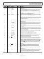
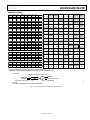
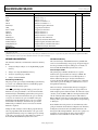
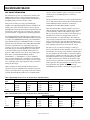
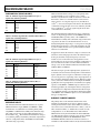
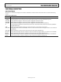
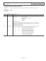
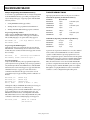
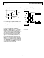
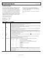
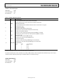
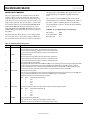
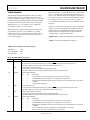
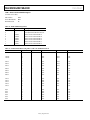
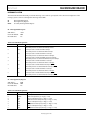
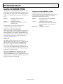
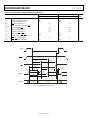
Table 63. CHIPID Values for Σ-Δ MicroConverter Products
a.
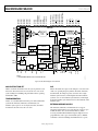
PLACE ANALOG
COMPONENTS
HERE
Part
ADuC816
ADuC824
ADuC836
ADuC834
ADuC845/ADuC847/ADuC848
PLACE DIGITAL
COMPONENTS
HERE
AGND
DGND
CHIPID
1xH
0xH
3xH
2xH
AxH
Clock Oscillator
b.
PLACE ANALOG
COMPONENTS
HERE
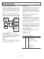
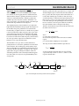
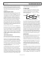
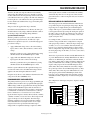
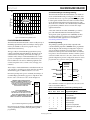
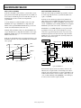
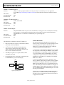
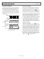
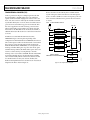
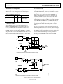
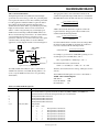
As described earlier, the core clock frequency for the ADuC845/
ADuC847/ADuC848 is generated from an on-chip PLL that
locks onto a multiple (384 times) of 32.768 kHz. The latter is
generated from an internal clock oscillator. To use the internal
clock oscillator, connect a 32.768 kHz parallel resonant crystal
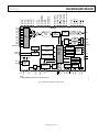
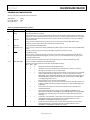
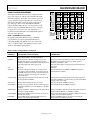
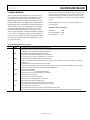
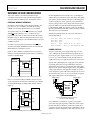
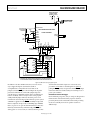
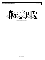
between XTAL1 and XTAL2 as shown in Figure 69.
PLACE DIGITAL
COMPONENTS
HERE
AGND
DGND
ADuC845/ADuC847/ADuC848
XTAL1
32
PLACE DIGITAL
COMPONENTS
HERE
GND
12pF
32.768kHz
TO INTERNAL PLL
33
XTAL2
12pF
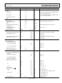
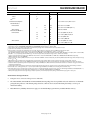
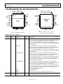
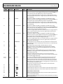
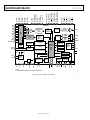
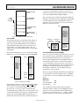
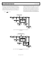
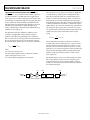
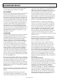
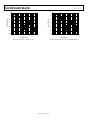
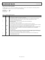
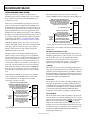
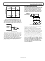
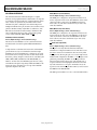
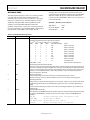
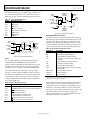
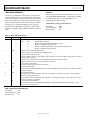
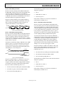
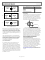
Figure 68. System Grounding Schemes
04741-065
PLACE ANALOG
COMPONENTS
HERE
04741-064
c.
Figure 69. Crystal Connectivity to ADuC845/ADuC847/ADuC848
If the user plans to connect fast logic signals (rise/fall time < 5 ns)
to any of the ADuC845/ADuC847/ADuC848’s digital inputs,
add a series resistor to each relevant line to keep rise and fall
times longer than 5 ns at the parts’ input pins. A value of 100 Ω
or 200 Ω is usually sufficient to prevent high speed signals from
coupling capacitively into the part and affecting the accuracy of
ADC conversions.
When using the LFCSP package, it is recommended that the
paddle underneath the chip be soldered to the board to provide
maximum mechanical stability. However, it is recommended
that this paddle not be grounded but left floating. All results
and specifications contained in this data sheet are taken or
recorded with the paddle floating.
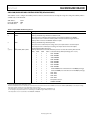
System Self-Identification
In some hardware designs, it may be advantageous for the
software to be able to identify the host MicroConverter.
The CHIPID SFR is a read-only register located at SFR address
C2H. The upper nibble of this SFR designates the MicroConverter
within the Σ-Δ ADC family. User software can read this SFR to
identify the host MicroConverter and therefore execute slightly
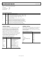
different code if required. The CHIPID SFR reads as follows for
the Σ-Δ ADC family of MicroConverter products. Note that the
ADuC845/ADuC847/ADuC848 are treated as one part as far as
the CHIPID is concerned.
As shown in the typical external crystal connection diagram in
Figure 69, two internal 12 pF capacitors are provided on-chip.
These are connected internally, directly to the XTAL1 and XTAL2
pins. The total input capacitance at both pins is detailed in the
Specifications table. Note that the total capacitance required for
a particular crystal must be in accordance with the crystal
manufacturer. However, in most cases, no additional external
capacitance is required above that already supplied on-chip.
OTHER HARDWARE CONSIDERATIONS
In-Circuit Serial Download Access
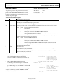
Nearly all ADuC845/ADuC847/ADuC848 designs can take
advantage of the in-circuit reprogrammability of the chip. This
is accomplished by a connection to the parts’ UART, which
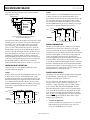
requires an external RS-232 chip for level translation if downloading code from a PC. Basic configuration of an RS-232
connection is shown in Figure 70 with a simple ADM3202based circuit. If users would rather not include an RS-232 chip
on the target board, refer to Application Note uC006,
“A 4-Wire UART-to-PC Interface” available at
www.analog.com/microconverter, for a simple (and zero-costper-board) method of gaining in-circuit serial download access
to the part.
Rev. C | Page 90 of 108