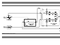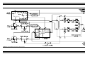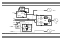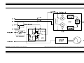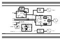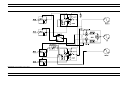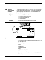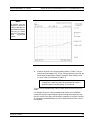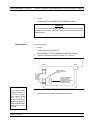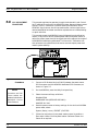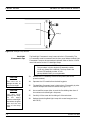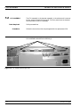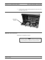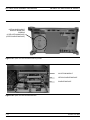
1
Caution
Do not exceed the operating input power level, voltage
level, current level, and signal type that is appropriate for
the instrument being used. Refer to your instrument’s operation manual for safe operating practices and device
limitations.
Electrostatic Discharge (ESD) can damage the highly
sensitive circuits in the instrument. ESD is most likely to
occur as test devices are being connected to, or disconnected from, the instrument’s front and rear panel ports
and connectors. You can protect the instrument and test
devices by wearing a static-discharge wristband. Alternatively, you can ground yourself to discharge any static
charge by touching the outer chassis of the grounded instrument before touching the instrument’s front and rear
panel ports and connectors. Avoid touching the test port
center conductors unless you are properly grounded and
have eliminated the possibility of static discharge.
Repair of damage that is found to be caused by electrostatic discharge is not covered under warranty.
MS462XX
VECTOR NETWORK MEASUREMENT SYSTEM
MAINTENANCE MANUAL
490 JARVIS DRIVE · MORGAN HILL, CA 95037-2809
P/N: 10410-00205
REVISION: H
PRINTED: JULY 2004
COPYRIGHT 2004 ANRITSU CO.
WARRANTY
The Anritsu product(s) listed on the title page is (are) warranted against defects in materials and
workmanship for three years from the date of shipment.
Anritsu's obligation covers repairing or replacing products which prove to be defective during the
warranty period. Buyers shall prepay transportation charges for equipment returned to Anritsu for
warranty repairs. Obligation is limited to the original purchaser. Anritsu is not liable for consequential
damages.
LIMITATION OF WARRANTY
The foregoing warranty does not apply to Anritsu connectors that have failed due to normal wear.
Also, the warranty does not apply to defects resulting from improper or inadequate maintenance by
the Buyer, unauthorized modification or misuse, or operation outside of the environmental
specifications of the product. No other warranty is expressed or implied, and the remedies provided
herein are the Buyer's sole and exclusive remedies.
TRADEMARK ACKNOWLEDGMENTS
V Connector and K Connector are registered trademarks of Anritsu Company.
HP 437B, HP 438A, DeskJet, and LaserJet are registered trademarks of Hewlett-Packard Company.
GPC-7 is a registered trademark of Amphenol Corporation.
Microsoft Excel, Notepad, and Windows are trademarks of Microsoft Corporation.
NOTICE
Anritsu Company has prepared this manual for use by Anritsu Company personnel and customers as
a guide for the proper installation, operation and maintenance of Anritsu Company equipment and
computer programs. The drawings, specifications, and information contained herein are the property
of Anritsu Company, and any unauthorized use or disclosure of these drawings, specifications, and
information is prohibited; they shall not be reproduced, copied, or used in whole or in part as the
basis for manufacture or sale of the equipment or software programs without the prior written
consent of Anritsu Company.
Safety Symbols
To prevent the risk of personal injury or loss related to equipment malfunction, Anritsu Company uses the
following symbols to indicate safety-related information. For your own safety, please read this information
carefully BEFORE operating the equipment.
Symbols Used in Manuals
DANGER
Indicates a very dangerous procedure that could result in serious injury or death if not performed properly.
WARNING
Indicates a hazardous procedure that could result in serious injury or
death if not performed properly.
CAUTION
Indicates a hazardous procedure or danger that could result in lightto-severe injury, or loss related to equipment malfunction, if proper
precautions are not taken.
Safety Symbols Used on Equipment and in Manuals
The following safety symbols are used inside or on the equipment near operation locations to provide information about safety items and operation precautions. Ensure that you clearly understand the meanings of
the symbols and take the necessary precautions BEFORE operating the equipment.
Some or all of the following five symbols may or may not be used on all Anritsu equipment. In addition, there
may be other labels attached to products that are not shown in the diagrams in this manual.
This symbol indicates a prohibited operation. The prohibited operation
is indicated symbolically in or near the barred circle.
This symbol indicates a compulsory safety precaution. The required
operation is indicated symbolically in or near the circle.
This symbol indicates warning or caution. The contents are indicated
symbolically in or near the triangle.
This symbol indicates a note. The contents are described in the box.
These symbols indicate that the marked part should be recycled.
MS462XX MM
SAFETY-1
For Safety
WARNING
Always refer to the operation manual when working near locations at
which the alert mark, shown on the left, is attached. If the operation, etc.,
is performed without heeding the advice in the operation manual, there is
a risk of personal injury. In addition, the equipment performance may be
reduced.
Moreover, this alert mark is sometimes used with other marks and descriptions indicating other dangers.
WARNING
When supplying AC power to this equipment, connect the accessory 3-pin
power cord to a 3-pin grounded power outlet. If a grounded 3-pin outlet is
not available, use a conversion adapter and ground the green wire, or
connect the frame ground on the rear panel of the equipment to ground. If
power is supplied without grounding the equipment, there is a risk of receiving a severe or fatal electric shock.
WARNING
Repair
This equipment cannot be repaired by the operator. DO NOT attempt to remove the equipment covers or to disassemble internal components. Only
qualified service technicians with a knowledge of electrical fire and shock
hazards should service this equipment. There are high-voltage parts in this
equipment presenting a risk of severe injury or fatal electric shock to untrained personnel. In addition, there is a risk of damage to precision components.
WARNING
If this equipment is used in a manner not specified by the manufacturer,
the protection provided by the equipment may be impaired.
SAFETY-2
MS462XX MM
Table of Contents, Narrative
Chapter 1—General Service Information
This chapter familiarizes the user with the basic MS462XX Vector Network Measurement System.
Included is information about related manuals, available models and options, preventive maintenance, recommended test equipment, replaceable assembly part numbers, and customer service
contact information.
Chapter 2—Theory of Operation
This chapter provides a brief overview of the functional assemblies and major parts that comprise
a typical MS462XX Vector Network Measurement System. It also briefly describes the operation of
each major assembly and includes system block diagrams.
Chapter 3—Operational Performance Tests
This chapter provides general operational tests for all instruments with most of the available
options.
Chapter 4—System Performance Verification
This chapter provides performance verification procedures for all non-C models.
Chapter 5—Adjustments
This chapter provides calibration procedures. Procedures include 10 MHz calibration, ALC adjustment, Back-end calibration, and Noise Source Internal Through Path characterization.
Chapter 6—Troubleshooting
This chapter provides information for troubleshooting MS462XX Vector Network Measurement
System. The troubleshooting procedures contained in this chapter support fault isolation down to a
replaceable subassembly.
Chapter 7—Removal and Replacement Procedures
This chapter describes how to gain access to all of the major assemblies and major parts for troubleshooting and/or replacement.
Appendix A—Connector Care and Handling
This appendix provides information on the proper care and handling of RF sensor connectors.
Appendix B—Performance Specifications
This appendix contains performance specifications.
Subject Index
MS462XX MM
i/ii
Table of Contents
Chapter 1 General Information
1-1
SCOPE OF THIS MANUAL . . . . . . . . . . . . . . . . . . . . . . . . . . . . . . 1-3
1-2
INTRODUCTION . . . . . . . . . . . . . . . . . . . . . . . . . . . . . . . . . . . 1-3
1-3
RELATED MANUALS. . . . . . . . . . . . . . . . . . . . . . . . . . . . . . . . . 1-3
1-4
MODELS . . . . . . . . . . . . . . . . . . . . . . . . . . . . . . . . . . . . . . . . 1-3
1-5
OPTIONS. . . . . . . . . . . . . . . . . . . . . . . . . . . . . . . . . . . . . . . . 1-4
1-6
IDENTIFICATION NUMBER. . . . . . . . . . . . . . . . . . . . . . . . . . . . . 1-4
1-7
SERVICE POLICY. . . . . . . . . . . . . . . . . . . . . . . . . . . . . . . . . . . 1-4
1-8
SPARE PARTS LISTING . . . . . . . . . . . . . . . . . . . . . . . . . . . . . . . 1-5
1-9
ASSEMBLY EXCHANGE PROGRAM . . . . . . . . . . . . . . . . . . . . . . . . 1-7
1-10
PREVENTIVE MAINTENANCE . . . . . . . . . . . . . . . . . . . . . . . . . . . 1-7
1-11
RECOMMENDED TEST EQUIPMENT . . . . . . . . . . . . . . . . . . . . . . . 1-7
1-12
CONVENTIONS . . . . . . . . . . . . . . . . . . . . . . . . . . . . . . . . . . . 1-10
1-13
COMPONENT HANDLING . . . . . . . . . . . . . . . . . . . . . . . . . . . . . 1-11
1-14
SERVICE CENTERS . . . . . . . . . . . . . . . . . . . . . . . . . . . . . . . . . 1-13
Chapter 2 Theory of Operation
2-1
INTRODUCTION . . . . . . . . . . . . . . . . . . . . . . . . . . . . . . . . . . . 2-3
2-2
SYSTEM OVERVIEW . . . . . . . . . . . . . . . . . . . . . . . . . . . . . . . . . 2-3
2-3
SOURCE MODULE . . . . . . . . . . . . .
Digital Interface . . . . . . . . . . . . .
Main Oscillator Loops . . . . . . . . . .
Offset Oscillator Loops . . . . . . . . .
DDS Reference Clock . . . . . . . . . .
Bounding Circuitry . . . . . . . . . . .
Speed-Up Circuitry . . . . . . . . . . .
Frequency Bands and Switched Filters.
Heterodyne Oscillator . . . . . . . . . .
ALC Circuitry . . . . . . . . . . . . . .
Operation Modes. . . . . . . . . . . . .
MS462XX MM
.
.
.
.
.
.
.
.
.
.
.
.
.
.
.
.
.
.
.
.
.
.
.
.
.
.
.
.
.
.
.
.
.
.
.
.
.
.
.
.
.
.
.
.
.
.
.
.
.
.
.
.
.
.
.
.
.
.
.
.
.
.
.
.
.
.
.
.
.
.
.
.
.
.
.
.
.
.
.
.
.
.
.
.
.
.
.
.
.
.
.
.
.
.
.
.
.
.
.
.
.
.
.
.
.
.
.
.
.
.
.
.
.
.
.
.
.
.
.
.
.
.
.
.
.
.
.
.
.
.
.
.
.
.
.
.
.
.
.
.
.
.
.
.
.
.
.
.
.
.
.
.
.
.
.
.
.
.
.
.
.
.
.
.
.
.
.
.
.
.
.
.
.
.
.
.
.
.
.
.
.
.
.
.
.
.
.
.
.
.
.
.
.
.
.
.
.
.
.
.
.
.
.
.
.
.
.
.
.
.
.
.
.
.
.
.
.
.
.
.
.
.
.
.
.
.
.
.
.
.
.
2-4
2-5
2-5
2-5
2-6
2-6
2-7
2-7
2-7
2-8
2-8
iii
Table of Contents (Continued)
2-4
RECEIVER MODULE . . . . . . . . . . . . . . . . . . . . . . . . . . . . . . . . 2-10
Down Conversion Module . . . . . . . . . . . . . . . . . . .
Digital Interface . . . . . . . . . . . . . . . . . . . . . . . .
Test Channel Intermediate Frequency Path . . . . . . . . .
Reference Channel Intermediate Frequency Path . . . . . .
Sampling of the Intermediate Frequency . . . . . . . . . . .
ADC Clock Generation/ DSP Communication Port Interface
10 MHz Clock Distribution . . . . . . . . . . . . . . . . . .
RF Component Control. . . . . . . . . . . . . . . . . . . . .
2-5
.
.
.
.
.
.
.
.
.
.
.
.
.
.
.
.
.
.
.
.
.
.
.
.
.
.
.
.
.
.
.
.
.
.
.
.
.
.
.
.
.
.
.
.
.
.
.
.
.
.
.
.
.
.
.
.
.
.
.
.
.
.
.
.
2-10
2-10
2-11
2-12
2-13
2-14
2-14
2-14
FRONT END RF COMPONENTS . . . . . . . . . . . . . . . . . . . . . . . . . . 2-15
Test Port Connectors . . . . . . . . . . . . . . . .
Switched Frequency Doubler Module . . . . . . .
Switched Frequency Tripler Module . . . . . . .
Auto-Reversing Module . . . . . . . . . . . . . .
Non-Reversing Module . . . . . . . . . . . . . . .
Step Attenuator . . . . . . . . . . . . . . . . . .
Port Module. . . . . . . . . . . . . . . . . . . . .
Port 3 Module. . . . . . . . . . . . . . . . . . . .
Low Noise Pre-Amplifier . . . . . . . . . . . . . .
Switched Module . . . . . . . . . . . . . . . . . .
High Isolation Switch Module . . . . . . . . . . .
Receiver Module Configurations. . . . . . . . . .
Receiver Module Configurations, MS462XA . . .
Receiver Module Configurations, MS462XB . . .
Receiver Module Configurations, MS462XC . . .
Receiver Module Configurations, MS462XD . . .
Option 3—Second Source . . . . . . . . . . . . .
Option 4—Noise Figure Measurement Capability
Option 6—Third Test Port . . . . . . . . . . . . .
iv
.
.
.
.
.
.
.
.
.
.
.
.
.
.
.
.
.
.
.
.
.
.
.
.
.
.
.
.
.
.
.
.
.
.
.
.
.
.
.
.
.
.
.
.
.
.
.
.
.
.
.
.
.
.
.
.
.
.
.
.
.
.
.
.
.
.
.
.
.
.
.
.
.
.
.
.
.
.
.
.
.
.
.
.
.
.
.
.
.
.
.
.
.
.
.
.
.
.
.
.
.
.
.
.
.
.
.
.
.
.
.
.
.
.
.
.
.
.
.
.
.
.
.
.
.
.
.
.
.
.
.
.
.
.
.
.
.
.
.
.
.
.
.
.
.
.
.
.
.
.
.
.
.
.
.
.
.
.
.
.
.
.
.
.
.
.
.
.
.
.
.
.
.
.
.
.
.
.
.
.
.
.
.
.
.
.
.
.
.
.
.
.
.
.
.
.
.
.
.
.
.
.
.
.
.
.
.
.
.
.
.
.
.
.
.
.
.
.
.
.
.
.
.
.
.
.
.
.
.
.
.
.
.
.
.
.
.
.
.
.
.
.
.
.
.
.
.
.
.
.
.
.
.
.
.
.
.
.
.
.
.
.
.
.
.
.
.
.
.
.
.
.
.
.
.
.
.
.
.
.
.
.
.
.
.
.
.
.
.
.
.
.
.
2-15
2-15
2-15
2-15
2-16
2-16
2-16
2-16
2-16
2-16
2-16
2-16
2-17
2-17
2-18
2-19
2-20
2-20
2-21
2-6
OPTION MODULES . . . . . . . . . . . . . . . . . . . . . . .
General . . . . . . . . . . . . . . . . . . . . . . . . . . . .
Frequency Translating Group Delay (FTGD) Synthesizer .
Frequency Translating Group Delay Receiver . . . . . . .
Wideband Noise Figure Receiver . . . . . . . . . . . . . .
.
.
.
.
.
.
.
.
.
.
.
.
.
.
.
.
.
.
.
.
.
.
.
.
.
.
.
.
.
.
.
.
.
.
.
.
.
.
.
.
.
.
.
.
.
.
.
.
.
.
2-21
2-21
2-22
2-23
2-23
2-7
CENTRAL PROCESSOR MODULE. . . . . . . . . . . . . . . . . . . . . . . . . 2-25
2-8
RECEIVER MODULE BLOCK DIAGRAMS . . . . . . . . . . . . . . . . . . . . 2-25
MS462XX MM
Table of Contents (Continued)
Chapter 3 Operational Performance Tests
3-1
INTRODUCTION . . . . . . . . . . . . . . . . . . . . . . . . . . . . . . . . . . . 3-3
3-2
CHECKING THE SERVICE LOG/SELF-TEST . . . . . . . . . . . . . . . . . . . 3-3
3-3
VERIFYING OUTPUT POWER ACCURACY . . . . . . . . . . . . . . . . . . . . 3-5
3-4
NON-RATIO PARAMETER TEST (MS462XA/C/D) . . . . . . . . . . . . . . . . . 3-7
3-5
SYSTEM DYNAMIC RANGE TEST (MS462XA/B/D) . . . . . . . . . . . . . . . 3-10
3-6
SYSTEM DYNAMIC RANGE TEST (MS462XC) . . . . . . . . . . . . . . . . . . 3-14
3-7
COMPRESSION LEVEL TEST (MS462XC) . . . . . . . . . . . . . . . . . . . . 3-16
3-8
RECEIVER MAGNITUDE DISPLAY LINEARITY TEST (MS462XC) . . . . . . 3-19
3-9
NOISE FIGURE MEASUREMENT CAPABILITY (OPTION 4) . . . . . . . . . . 3-26
Noise Figure Assurance Check . . . . . . . . . . . . . . . . . . . . . . . . . 3-26
Raw Receiver Noise Figure Check . . . . . . . . . . . . . . . . . . . . . . . . 3-26
3-10
NOISE FIGURE MEASUREMENT CONFIDENCE CHECK . . . . . . . . . . . 3-30
3-11
FREQUENCY TRANSLATING GROUP DELAY (OPTION 5) . . . . . . . . . . . 3-35
3-12
37SF50 PHASE HARMONIC STANDARDS OPERATIONAL CHECK . . . . . . 3-36
Input and Output Return Loss Check . . . . . . . . . . . . . . . . . . . . . . 3-36
3-13
HARMONIC OUTPUT CHECK . . . . . . . . . . . . . . . . . . . . . . . . . . . 3-39
Chapter 4 System Performance Verification
4-1
INTRODUCTION . . . . . . . . . . . . . . . . . . . . . . . . . . . . . . . . . . . 4-3
4-2
CALIBRATION AND MEASUREMENT CONDITIONS . . . . . . . . . . . . . . 4-4
Standard Conditions. . . . . . . . . . . . . . . . . . . . . . . . . . . . . . . . 4-4
Special Precautions . . . . . . . . . . . . . . . . . . . . . . . . . . . . . . . . 4-4
4-3
PERFORMANCE VERIFICATION FOR THE MS462XA/B/D MODELS . . . . . . 4-5
2300-482 Software Requirements . . . . . . . . . . . . . . . . . . . . . . . . . 4-5
2300-482 Verification Software Overview . . . . . . . . . . . . . . . . . . . . 4-6
4-4
VNMS TRACEABILITY . . . . . . . . . . . . . . . . . . . . . . . . . . . . . . . . 4-7
Chapter 5 Adjustments
5-1
INTRODUCTION . . . . . . . . . . . . . . . . . . . . . . . . . . . . . . . . . . . 5-3
5-2
RECOMMENDED TEST EQUIPMENT . . . . . . . . . . . . . . . . . . . . . . . 5-4
5-3
TEST CONDITIONS. . . . . . . . . . . . . . . . . . . . . . . . . . . . . . . . . . 5-4
5-4
PRE-TEST SETUP. . . . . . . . . . . . . . . . . . . . . . . . . . . . . . . . . . . 5-4
5-5
10 MHz CALIBRATION PROCEDURE . . . . . . . . . . . . . . . . . . . . . . . 5-4
Manual Calibration Procedure: . . . . . . . . . . . . . . . . . . . . . . . . . . 5-6
MS462XX MM
v
Table of Contents (Continued)
5-6
ALC ADJUSTMENT PROCEDURE . . . . . . . . . . . . . . . . . . . . . . . . . 5-8
5-7
BACK-END ATTENUATOR CALIBRATION (OPTION 4X ONLY) . . . . . . . . 5-10
5-8
NOISE SOURCE SIGNAL INTERNAL THROUGH PATH
CHARACTERIZATION (OPTION 4X ONLY) . . . . . . . . . . . . . . . . . . . . 5-11
Chapter 6 Troubleshooting
6-1
INTRODUCTION . . . . . . . . . . . . . . . . . . . . . . . . . . . . . . . . . . . 6-3
6-2
SELF TEST . . . . . . . . . . . . . . . . . . . . . . . . . . . . . . . . . . . . . . 6-3
6-3
TROUBLESHOOTING TOOLS FOR THE CPU MODULE
SRAM . . . . . . . . . . . . . . . . . . . . . . . . . .
SRAM DISK . . . . . . . . . . . . . . . . . . . . . . .
FLASH MEMORY . . . . . . . . . . . . . . . . . . . .
EXTENDED FLASH MEMORY . . . . . . . . . . . .
DRAM . . . . . . . . . . . . . . . . . . . . . . . . . .
GRAPHICS VRAM . . . . . . . . . . . . . . . . . . .
GRAPHICS DRAM . . . . . . . . . . . . . . . . . . .
DSP SRAM . . . . . . . . . . . . . . . . . . . . . . . .
6-4
HARDWARE TROUBLESHOOTING. . . . . . . . . . . . . . . . . . . . . . . . . 6-8
.
.
.
.
.
.
.
.
.
.
.
.
.
.
.
.
.
.
.
.
.
.
.
.
.
.
.
.
.
.
.
.
.
.
.
.
.
.
.
.
.
.
.
.
.
.
.
.
.
.
.
.
.
.
.
.
.
.
.
.
.
.
.
.
.
.
.
.
.
.
.
.
.
.
.
.
.
.
.
.
.
.
.
.
.
.
.
.
.
.
.
.
.
.
.
.
.
.
.
.
.
.
.
.
.
.
.
.
.
.
.
.
.
.
.
.
.
6-4
6-6
6-6
6-6
6-6
6-7
6-7
6-7
6-7
CPU MODULE . . . . . . . . . . . . . . . . . . . . . . . . . . . . . . . . . . 6-8
SOURCE MODULE . . . . . . . . . . . . . . . . . . . . . . . . . . . . . . . . 6-9
HET OSCILLATOR VOLTAGE . . . . . . . . . . . . . . . . . . . . . . . . . 6-11
SOURCE 1 . . . . . . . . . . . . . . . . . . . . . . . . . . . . . . . . . . . . 6-12
SOURCE 2 . . . . . . . . . . . . . . . . . . . . . . . . . . . . . . . . . . . . 6-12
LO . . . . . . . . . . . . . . . . . . . . . . . . . . . . . . . . . . . . . . . . . 6-12
AUTO LEVEL CONTROL (ALC) . . . . . . . . . . . . . . . . . . . . . . . . 6-13
RECEIVER MODULE . . . . . . . . . . . . . . . . . . . . . . . . . . . . . . 6-16
NOISE SOURCE POWER SUPPLY. . . . . . . . . . . . . . . . . . . . . . . 6-21
POWER DISTRIBUTION UNIT. . . . . . . . . . . . . . . . . . . . . . . . . 6-21
FRONT PANEL ASSEMBLY . . . . . . . . . . . . . . . . . . . . . . . . . . 6-22
vi
6-5
SOFTWARE PROBLEM . . . . . . . . . . . . . . . . . . . . . . . . . . . . . . . 6-23
6-6
MEASUREMENT QUALITY PROBLEM . . . . . . . . . . . . . . . . . . . . . . 6-23
6-7
NOISE FIGURE MEASUREMENT PROBLEM . . . . . . . . . . . . . . . . . . 6-24
6-8
FREQUENCY TRANSLATING GROUP DELAY MEASUREMENT . . . . . . . 6-27
MS462XX MM
Table of Contents (Continued)
Chapter 7 Removal and Replacement Procedures
7-1
INTRODUCTION . . . . . . . . . . . . . . . . . . . . . . . . . . . . . . . . . . . 7-3
7-2
FRONT PANEL . . . . . . . . . . . . . . . . . . . . . . . . . . . . . . . . . . . . 7-4
Floppy Disk Drive Assembly
LCD Assembly . . . . . . . .
LCD Backlight Driver PCB .
Interface PCB . . . . . . . .
Backlight Fluorescent Lamp
7-3
.
.
.
.
.
.
.
.
.
.
.
.
.
.
.
.
.
.
.
.
.
.
.
.
.
.
.
.
.
.
.
.
.
.
.
.
.
.
.
.
.
.
.
.
.
.
.
.
.
.
.
.
.
.
.
.
.
.
.
.
.
.
.
.
.
.
.
.
.
.
.
.
.
.
.
.
.
.
.
.
.
.
.
.
.
.
.
.
.
.
.
.
.
.
.
.
.
.
.
.
.
.
.
.
.
.
.
.
.
.
.
.
.
.
.
.
.
.
.
.
.
.
.
.
.
.
.
.
.
.
.
.
.
.
.
7-6
7-6
7-7
7-7
7-8
POWER DISTRIBUTION UNIT . . . . . . . . . . . . . . . . . . . . . . . . . . . 7-9
PDU Fuse . . . . . . . . . . . . . . . . . . . . . . . . . . . . . . . . . . . . . 7-11
7-4
CPU ASSEMBLY . . . . . . .
System Firmware PROM
CPU Heatsink with Fan .
Lithium Battery . . . . .
.
.
.
.
.
.
.
.
.
.
.
.
.
.
.
.
.
.
.
.
.
.
.
.
.
.
.
.
.
.
.
.
.
.
.
.
.
.
.
.
.
.
.
.
.
.
.
.
.
.
.
.
.
.
.
.
.
.
.
.
.
.
.
.
.
.
.
.
.
.
.
.
.
.
.
.
.
.
.
.
.
.
.
.
.
.
.
.
.
.
.
.
.
.
.
.
.
.
.
.
.
.
.
.
.
.
.
.
.
.
.
.
7-12
7-14
7-15
7-15
7-5
RECEIVER MODULE ASSEMBLY . . . . . . . . . . . . . . . . . . . . . . . . . 7-18
7-6
TEST PORT CONNECTOR AND PORT MODULE . . . . . . . . . . . . . . . . 7-20
7-7
OPTION AND SOURCE MODULES . . . . . . . . . . . . . . . . . . . . . . . . 7-21
7-8
BACKPLANE PCB ASSEMBLY . . . . . . . . . . . . . . . . . . . . . . . . . . . 7-23
Appendix A Connector Care and Handling
A-1
INTRODUCTION . . . . . . . . . . . . . . . . . . . . . . . . . . . . . . . . . . . A-3
A-2
CONNECTOR CARE AND HANDLING . . . . . . . . . . .
Beware of Destructive Pin Depth of Mating Connectors.
Avoid Over-Torquing Connectors . . . . . . . . . . . . .
Cleaning Connectors . . . . . . . . . . . . . . . . . . .
.
.
.
.
.
.
.
.
.
.
.
.
.
.
.
.
.
.
.
.
.
.
.
.
.
.
.
.
.
.
.
.
.
.
.
.
.
.
.
.
.
.
.
.
.
.
.
.
A-3
A-3
A-4
A-5
Appendix B Performance Specifications
Subject Index
MS462XX MM
vii/viii
Chapter 1
General Information
Table of Contents
Chapter 1 General Information
1-1
SCOPE OF THIS MANUAL . . . . . . . . . . . . . . . . . . . . . . . . . . . . . . 1-3
1-2
INTRODUCTION . . . . . . . . . . . . . . . . . . . . . . . . . . . . . . . . . . . 1-3
1-3
RELATED MANUALS. . . . . . . . . . . . . . . . . . . . . . . . . . . . . . . . . 1-3
1-4
MODELS . . . . . . . . . . . . . . . . . . . . . . . . . . . . . . . . . . . . . . . . 1-3
1-5
OPTIONS. . . . . . . . . . . . . . . . . . . . . . . . . . . . . . . . . . . . . . . . 1-4
1-6
IDENTIFICATION NUMBER. . . . . . . . . . . . . . . . . . . . . . . . . . . . . 1-4
1-7
SERVICE POLICY. . . . . . . . . . . . . . . . . . . . . . . . . . . . . . . . . . . 1-4
1-8
SPARE PARTS LISTING . . . . . . . . . . . . . . . . . . . . . . . . . . . . . . . 1-5
1-9
ASSEMBLY EXCHANGE PROGRAM . . . . . . . . . . . . . . . . . . . . . . . . 1-7
1-10
PREVENTIVE MAINTENANCE . . . . . . . . . . . . . . . . . . . . . . . . . . . 1-7
1-11
RECOMMENDED TEST EQUIPMENT . . . . . . . . . . . . . . . . . . . . . . . 1-7
1-12
CONVENTIONS . . . . . . . . . . . . . . . . . . . . . . . . . . . . . . . . . . . 1-10
1-13
COMPONENT HANDLING . . . . . . . . . . . . . . . . . . . . . . . . . . . . . 1-11
1-14
SERVICE CENTERS . . . . . . . . . . . . . . . . . . . . . . . . . . . . . . . . . 1-13
Figure 1-1. MS462XX Vector Network Measurement System
1-2
MS462XX MM
Chapter 1
General Information
1-1
1-2
1-3
1-4
SCOPE OF THIS
MANUAL
This manual provides general information, performance verification, calibration, theory, and service information for the Anritsu MS462XX Vector
Network Measurement System. The MS462XX Vector Network Measurement System is shown in Figure 1-1 (facing page).
INTRODUCTION
This chapter provides information to familiarize the user with the basic
MS462XX Vector Network Measurement System. Included is information
about related manuals, and the available models and options.
RELATED
MANUALS
This manual is one of a five manual set consisting of this Maintenance
Manual, the MS462XX Operation Manual (Anritsu part number
10410-00203), the MS462XX Programming Manual (10410-00204), the
MS462XX Scorpion Measurement Guide (10410-00213), and the MS462XX
GPIB Quick Reference Guide (10410-00206).
MODELS
With twelve basic models and a number of powerful options to choose
from, the MS462XX can be configured to address many measurement requirements. The following models are available as platforms:
Model Number
Frequency Range
Configuration
MS4622A
10 MHz to 3 GHz
Transmission/Reflection
MS4622B
10 MHz to 3 GHz
Full Reversing
MS4622C
10 MHz to 3 GHz
Direct Receiver Access
MS4622D
10 MHz to 3 GHz
Balanced/Differential
MS4623A
10 MHz to 6 GHz
Transmission/Reflection
MS4623B
10 MHz to 6 GHz
Full Reversing
MS4623C
10 MHz to 6 GHz
Direct Receiver Access
MS4623D
10 MHz to 6 GHz
Balanced/Differential
MS4624A
10 MHz to 9 GHz
Transmission/Reflection
MS4624B
10 MHz to 9 GHz
Full Reversing
MS4624C
10 MHz to 9 GHz
Direct Receiver Access
MS4624D
10 MHz to 9 GHz
Balanced/Differential
The Transmission/Reflection models offer an economical solution for the
manufacturing line that requires only S11 and S21 measurements without
sacrificing the excellent performance of the Full Reversing models.
MS462XX MM
1-3
OPTIONS
1-5
OPTIONS
GENERAL INFORMATION
The following options are easily added to the MS462XX platform for increased measurement capabilities:
Option Number
Description
Availability
2
Time Domain
All Models
3A
Second Internal Source4
3 GHz Source – B Models
3B
Second Internal Source4
6 GHz Source – B Models
3C
Second Internal Source5
3 GHz Source – C Models
3D
Second Internal Source5
6 GHz Source – C Models
3E
Second Internal Source7
9 Ghz Source – D Models
3F
Second Internal Source7
9 Ghz Source – C Models
4, 4D, 4F
Noise Figure1
B, C and D Models Only
4B, 4E, 4G
Noise Figure6
B, C and D Models Only
5
Frequency Translating
Group Delay
B and C Models Only
6
Third Test Port3
B and C Models Only
7
T/R Step Attenuator
A Models Only
8
Harmonic Measurement
All Models
10
AutoCal Control
All Models
11
Test Port Connector
All Models 2
13
Intermodulation Distortion
All Models
24
Processing Upgrade
B and C Models Only
1. 50 MHz to 3 GHz
2. Standard Connector is N-female, No cost option for 3.5 mm (male), 3.5 mm (female),
N-Male, or GPC-7.
3. Requires external source, 68XXX Synthesizer
4. Third test port included
5. Third output port included
6. 50 MHz to 6 Ghz
7. Third and Fourth output port included
1-6
1-7
IDENTIFICATION
NUMBER
The MS462XX Vector Network Measurement System’s ID number is affixed to the rear panel. Please use the complete ID number when ordering
parts or corresponding with the Anritsu Customer Service department.
SERVICE POLICY
The MS462XX Vector Network Measurement System’s modular design,
extensive built-in diagnostics, and automated service tools are designed
to support fast exchange of functional assembly level repairs.
Failed assemblies are not field repairable. Once an assembly is found to
be faulty, it should be returned to an authorized Anritsu Service Center
(Table 1-4) for exchange.
1-4
MS462XX MM
GENERAL INFORMATION
1-8
SPARE PARTS
LISTING
SPARE PARTS LISTING
The assemblies and spare parts listed in Table 1-1 through Table 1-3 are
available for the MS462XX Vector Network Measurement System. Refer to
Chapter 7 for removal and replacement procedures. Contact your nearest
Anritsu Customer Service or Sales Center for price and availability information (Table 1-4).
Table 1-1. Assemblies Common to All MS462XX Instruments
Description
MS462XX MM
Part Number
Main Source Module
52392
Optional Source Module
52393
CPU Board
See Table 1-3
CPU Heatsink with Fan
650-34
CPU Boot PROM
58-1638
Lithium Battery (for CPU)
633-25
Receiver PCB
See Table 1-3
Power Supply (PDU) Entire
ND55521
Power Supply Fan Assembly
ND49520
Power Supply Fuse
631-90
Option Module Assembly
ND56500
Floppy Drive
ND50711
LCD Display
15-100
LCD Backlight Driver PCB
2000-770
LCD Window (Plastic shield)
48177
Lamp for Sharp LQ9D340 LCD
632-55
Chassis (Instrument frame)
D43325
Front Panel PCB, Keypad, Knob for 2 or 3 Ports
ND48996
Front Panel PCB, Keypad, Knob for 4 Ports
ND58272
Backplane PCB
48522-4
Test Port Connector (N Female)
B45259
Test Port Connector (N Male)
B45261
Test Port Connector (GPC-7)
B47086
Test Port Connector (3.5mm Male)
B47088
Test Port Connector (3.5mm F)
B47087
Operating Software
2300-244
Boot Utility Software
2300-246
Handle, Standard (Right)
D37169-4
Handle, Standard (Left)
D37168-4
1-5
SPARE PARTS LISTING
GENERAL INFORMATION
Table 1-2. Replaceable Internal Microwave Components
Description
Part Number
AutoReverse Module (9 GHz units)
54530
AutoReverse Module (3 and 6 GHz units)
44666
Source Doubler Module (3 and 6 GHz units)
28875
Down Converter Module (3 and 6 GHz units)
29830
Down Converter Module (9 GHz units)
54610
Port 3 Module (all units)
44668
Port 1, 2 Module (all units)
46720
Tripler Module (9 GHz units)
56630
Hi Iso Switch (3 and 6 GHz units)
53077
Hi Iso Switch (9 GHz units)
60261
Non-Reversing Module (all units)
49983
Low Noise Amp for Opt. 4 (3 and 6 GHz units)
53300
Switch Module for Opt. 4 (3 and 6 GHz units)
46718
Table 1-3. Model-Specific Exchange Kits
Model
Receiver PCB Exchange
Kit
CPU Exchange Kit
MS4622A
ND49524
ND55522
MS4622B
ND49524
ND55522 *
MS4622C
ND53277
ND55522 *
MS4622D (without Opt.4)
ND57968
ND57970
MS4622D (with Opt.4)
ND60706
ND57970
MS4623A
ND49524
ND55522
MS4623B
ND49524
ND55522 *
MS4623C
ND53277
ND55522 *
MS4623D (without Opt.4)
ND57968
ND57970
MS4623D (with Opt.4)
ND60706
ND57970
MS4624A
ND55524
ND55522 *
MS4624B
ND55524
ND55522 *
MS4624C
ND60331
ND55522 *
MS4624D (without Opt.4)
ND57968
ND57970
MS4624D (with Opt.4)
ND60706
ND57970
* Use ND55522 if Option 24 is not installed. Use ND57970 if Option 24 is installed.
1-6
MS462XX MM
GENERAL INFORMATION
1-9
ASSEMBLY
EXCHANGE
PROGRAM
ASSEMBLY EXCHANGE PROGRAM
Anritsu maintains an exchange assembly program for selected MS462XX
subassemblies and RF components. If a malfunction occurs in one of these
subassemblies, the defective unit can be exchanged. All exchange subassemblies or RF components are warrantied for 90 days from the date of shipment,
or the balance of the original equipment warranty, whichever is longer. A
hard copy or saved to disk copy of the instrument Service Log must accompany all exchange modules. To access the Service Log, press the Utility front
panel key, followed by the SERVICE LOG menu soft key. Select either PRINT
LOG or SAVE LOG TO DISK.
NOTE
When sending an assembly to the factory for exchange, a
copy of the Service Log must accompany the assembly. Exchange prices can only be offered if the Service Log data is
included with the assembly to be exchanged.
Please have the exact model number and serial number of your unit available
when requesting this service, as the information about your system is filed
according to the instrument model and serial number. For more information
about the assembly exchange program, contact your local sales representative
or call your local Anritsu Service Center. Refer to Table 1-4 for a list of current Anritsu Service Centers.
1-10
PREVENTIVE
MAINTENANCE
The MS462XX CPU module contains a battery-backed memory/real time
clock chip (BBRAM) and a static memory (SRAM) backup battery. The
BBRAM chip has a rated life span of 10 years, and the SRAM backup battery
has a worst-case life span of two years at 25°C when the instrument is stored
(always off). Exposure to temperatures above 60°C will dramtically reduce
this worst-case life span. The SRAM backup battery should be replaced every
three years.
For instruments with serial number 995299 and below, the LCD (Anritsu part
number 15-92) contains a backlight flourescent lamp that has a rated 10,000
hour life span. For instruments with serial number 000101 and above, the
LCD (Anritsu part number 15-100) contains a backlight flourescent lamp that
has a rated 50,000 hour life span. Both the SRAM backup battery and
backlight lamp should be replaced periodically per the procedures in Chapter 7.
1-11
RECOMMENDED
TEST
EQUIPMENT
MS462XX MM
The following test equipment is recommended for servicing the MS462XX
Vector Network Measurement System. The list is a suggestion and by no
means comprises a comprehensive list of all equipment necessary to service
this system. Functionally equivalent equipment may be substituted for the
recommended manufacturer or model as long as the critical specifications are
met. Inclusion on this list does not constitute an endorsement or suitability of
purpose of any particular equipment or manufacturer. The Application Code
column of the following table represents when or where the specified equipment would be used:
1-7
RECOMMENDED TEST EQUIPMENT
Instrument
Computer or
Controller
Critical Specifications
GENERAL INFORMATION
Recommended
Manufacturer or Model
Application
Code
O, P
Personal Computer:
Pentium class processor, Win 95
(16 MB RAM min.)
Any Desktop PC:
GPIB Interface
National Instruments
PCI-GPIB or AT-GPIB/TNT
(plug-and-play)
Notebook PC:
National Instruments
PCMCIA-GPIB
Performance
Verification
Software
Anritsu 2300-482
P
Anritsu 2100-X
O, P, A
Any
O
Anritsu ND51900
O
(3 each)
Anritsu 3670A50-2,
3670K50-2, 3670N50-2,
3670NN50-2
O, P
N test port connector
Anritsu 3753LF/3753R with
Option 1 and 3
O, P
3.5 mm test port
connector
Anritsu 3750LF/3750R with
Option 1 and 3
O, P
GPC-7 test port
connector
Anritsu 3751LF/3751R with
Option 3
O, P
Two each of:
N male test port
N female test port
3.5mm male test port
3.5mm female test port
GPC-7 test port
Anritsu 23NF50
Anritsu 23N50
Anritsu 23LF50
Anritsu 23L50
Anritsu 23A50
GPIB Cable
RF/Microwave
Cable
DC to 6 GHz, K or 3.5
mm connectors (male
or female)
Printer Port
Test
Throughline
Calibration Kit
Short
Verification Kit
Frequency
Counter
1-8
O
N test port connector
3.5mm test port connector
GPC-7 test port connector
Anritsu 3663LF/3663R
Anritsu 3666LF/3666R
Frequency: 1 to 20 GHz
Input Impedance: 50 W
Frequency Stability:
-7
Temperature = 1x10
Anritsu MF2412B or
EIP Microwave, Inc.,
Model 548B
P
Anritsu 3667LF/3667R
A
MS462XX MM
GENERAL INFORMATION
Instrument
RECOMMENDED TEST EQUIPMENT
Critical Specifications
Recommended
Manufacturer or Model
Application
Code
Power Meter:
Power Range –70 to
+20 dBm
GPIB controllable
Anritsu ML2430A Series
Power Sensor:
Frequency Range
10 MHz to 18 GHz
Power Range –70 to
+20 dBm
Anritsu MA2472A
Digital
Multimeter
Resolution: 4 ½ digits
DC Accuracy: 0.1 %
AC Accuracy: 0.1 %
Any
T
Oscilloscope
Bandwidth :
DC to 100 MHz
Tektronix Inc., Model 2445
T
Power Meter
and Sensor
O, A, P
Sensitivity: 2 mV
Horiz. Sensitivity:
50 ns/division
Power Supply
Voltage: +12V
Current: 100 mA min.
Any
O
Power
Amplifier
Gain: 10 dB min.
Noise Figure: 5.5 dB
typical
Mini-Circuit
ZJL-4G (4 GHz) APN:60-242
ZJL-6G (6 GHz) APN:60-234
O
Noise Source
15 dB ENR
Anritsu NC346B
O
Step
Attenuator
With calibration data at
50 MHz
Anritsu MN510C
P
Attenuator
10 dB
Anritsu 43KC-10
P
Application Codes:
A = Adjustment / Internal Hardware Calibration
O = Operational Testing
P = Performance Verification
T = Troubleshooting
MS462XX MM
1-9
CONVENTIONS
1-12
CONVENTIONS
GENERAL INFORMATION
Throughout this manual, path names may be used to represent the keystrokes for a desired action or procedure. The path name begins with a front
panel key selection, followed by additional front panel or soft key selections,
each separated by a forward slash (/). Front panel key names and soft keys
are presented in the manual as they are on the system, that is, in initial caps
or all uppercase letters as appropriate. For example, the following path name
representation displays the system model number, serial number, current
software version, and installed options:
Utility/INSTRUMENT STATE PARAMETERS/SYSTEM
Following the path above, the user would press the Utility front panel key, followed by the INSTRUMENT STATE PARAMETERS soft key, then the SYSTEM
soft key to display the system information.
Individual steps within a procedure may also be presented as sequentially
numbered steps for clarity. Again, front panel key names and soft keys are
presented in the manual as they are on the system. For example, the following procedure displays the system model number, serial number, current software version, and installed options:
1.
Press the Utility front panel key.
2.
Select the menu soft keys as follows:
INSTRUMENT STATE PARAMETERS
SYSTEM
1-10
MS462XX MM
GENERAL INFORMATION
1-13
COMPONENT
HANDLING
COMPONENT HANDLING
The MS462XX series contains components that can be damaged by static
electricity. The following figures illustrate the precautions that should be
followed when handling static-sensitive subassemblies and components.
If followed, these precautions will minimize the possibilities of staticshock damage to these items.
NOTE
Use of a grounded wrist strap when removing and/or replacing subassemblies or parts is strongly recommended.
1. Do not touch exposed contacts on any
static sensitive component.
2. Do not slide static sensitive component across any surface.
3. Do not handle static sensitive components in areas where the floor or work
surface covering is capable of generating a static charge.
4. Wear a static-discharge wristband
when working with static sensitive
components.
5. Label all static sensitive devices.
6. Keep component leads shorted together whenever possible.
MS462XX MM
1-11
COMPONENT HANDLING
7. Handle PCBs only by their edges. Do
not handle by the edge connectors.
GENERAL INFORMATION
8. Lift & handle solid state devices by
their bodies—never by their leads.
9. Transport and store PCBs and other
static sensitive devices in staticshielded containers.
ADDITIONAL PRECAUTIONS
Keep work spaces clean and free of any objects capable of holding or storing a static charge.
Connect soldering tools to an earth ground.
Use only special anti-static suction or wick-type desoldering tools.
CAUTION
Electrostatic Discharge (ESD) can damage the highly sensitive circuits in
the MS462XX VNMS. ESD is most likely to occur as test devices are being connected to, or disconnected from, the instrument’s front and rear
panel ports and connectors. You can protect the instrument and test devices by wearing a static-discharge wristband. Alternatively, you can
ground yourself to discharge any static charge by touching the outer
chassis of the grounded instrument before touching the intrument’s front
and rear panel ports and connectors. Avoid touching the test port center
conductors unless you are properly grounded and have eliminated the
possibility of static discharge.
Repair of damage that is found to be caused by ESD is not covered under
warranty.
1-12
MS462XX MM
GENERAL INFORMATION
1-14
SERVICE CENTERS
SERVICE
CENTERS
Table 1-4. Anritsu Service Centers
UNITED STATES
FRANCE
JAPAN
ANRITSU COMPANY
490 Jarvis Drive
Morgan Hill, CA 95037-2809
Telephone: (408) 776-8300
1-800-ANRITSU
FAX: 408-776-1744
ANRITSU S.A
9 Avenue du Quebec
Zone de Courtaboeuf
91951 Les Ulis Cedex
Telephone: 016-09-21-550
FAX: 016-44-61-065
ANRITSU CUSTOMER SERVICES LTD.
1800 Onna Atsugi-shi
Kanagawa-Prf. 243 Japan
Telephone: 0462-96-6688
FAX: 0462-25-8379
GERMANY
SINGAPORE
ANRITSU GmbH
Grafenberger Allee 54-56
D-40237 Dusseldorf, Germany
Telephone: 0211-968550
FAX: 0211-9685555
ANRITSU (SINGAPORE) PTE LTD.
10, Hoe Chiang Road
#07-01/02 Keppel Towers
Singapore 089315
Telephone: 6-282-2400
FAX: 6-282-2533
ANRITSU COMPANY
10 New Maple Ave., Unit 305
Pine Brook, NJ 07058
Telephone: (973) 227-8999
1-800-ANRITSU
FAX: 973-575-0092
INDIA
SOUTH AFRICA
ANRITSU COMPANY
1155 E. Collins Blvd
Richardson, TX 75081
Telephone: 1-800-ANRITSU
FAX: 972-671-1877
MEERA AGENCIES PVT. LTD.
23 Community Centre
Zamroodpur, Kailash Colony Extension,
New Delhi, India 110 048
Phone: 011-2-6442700/6442800
FAX : 011-2-644250023
ETECSA
12 Surrey Square Office Park
330 Surrey Avenue
Ferndale, Randburt, 2194
South Africa
Telephone: 011-27-11-787-7200
FAX: 011-27-11-787-0446
AUSTRALIA
ISRAEL
SWEDEN
ANRITSU PTY. LTD.
Unit 3, 170 Foster Road
Mt Waverley, VIC 3149
Australia
Telephone: 03-9558-8177
FAX: 03-9558-8255
TECH-CENT, LTD.
4 Raul Valenberg St
Tel-Aviv 69719
Telephone: (03) 64-78-563
FAX: (03) 64-78-334
ANRITSU AB
Borgafjordsgatan 13
164 40 KISTA, Sweden
Telephone: +46-8-53470700
FAX: +46-8-53470730
BRAZIL
ITALY
TAIWAN
ANRITSU ELECTRONICA LTDA.
Praia de Botafogo, 440, Sala 2401
CEP22250-040, Rio de Janeiro, RJ, Brasil
Telephone: 021-527-6922
FAX: 021-53-71-456
ANRITSU Sp.A
Roma Office
Via E. Vittorini, 129
00144 Roma EUR
Telephone: (06) 50-99-711
FAX: (06) 50-22-425
ANRITSU CO., INC.
7F, No. 316, Section 1
NeiHu Road
Taipei, Taiwan, R.O.C.
Telephone: 886-2-8751-1816
FAX: 886-2-8751-2126
CANADA
KOREA
UNITED KINGDOM
ANRITSU INSTRUMENTS LTD.
700 Silver Seven Road, Suite 120
Kanata, Ontario K2V 1C3
Telephone: (613) 591-2003
FAX: (613) 591-1006
ANRITSU CORPORATION LTD.
8F Hyunjuk Building, 832-41
Yeoksam Dong, Kangnam-Ku
Seoul, South Korea 135-080
Telephone: 02-553-6603
FAX: 02-553-6605
ANRITSU LTD.
200 Capability Green
Luton, Bedfordshire
LU1 3LU, England
Telephone: 015-82-433200
FAX: 015-82-731303
CHINA
ANRITSU ELECTRONICS (SHANGHAI) CO. LTD.
2F, Rm B, 52 Section Factory Building
No. 516 Fu Te Rd (N)
Shanghai 200131 P.R. China
Telephone:21-58680226, 58680227, 58680228
FAX: 21-58680588
MS462XX MM
1-13/1-14
Chapter 2
Theory of Operation
Table of Contents
2-1
INTRODUCTION . . . . . . . . . . . . . . . . . . . . . . . . . . . . . . . . . . . 2-3
2-2
SYSTEM OVERVIEW . . . . . . . . . . . . . . . . . . . . . . . . . . . . . . . . . 2-3
2-3
SOURCE MODULE . . . . . . . . . . . . . . . . . . . . . . . . . . . . . . . . . . 2-4
Digital Interface . . . . . . . . . . . . .
Main Oscillator Loops . . . . . . . . . .
Offset Oscillator Loops . . . . . . . . .
DDS Reference Clock . . . . . . . . . .
Bounding Circuitry . . . . . . . . . . .
Speed-Up Circuitry . . . . . . . . . . .
Frequency Bands and Switched Filters.
Heterodyne Oscillator . . . . . . . . . .
ALC Circuitry . . . . . . . . . . . . . .
Operation Modes. . . . . . . . . . . . .
2-4
.
.
.
.
.
.
.
.
.
.
.
.
.
.
.
.
.
.
.
.
.
.
.
.
.
.
.
.
.
.
.
.
.
.
.
.
.
.
.
.
.
.
.
.
.
.
.
.
.
.
.
.
.
.
.
.
.
.
.
.
.
.
.
.
.
.
.
.
.
.
.
.
.
.
.
.
.
.
.
.
.
.
.
.
.
.
.
.
.
.
.
.
.
.
.
.
.
.
.
.
.
.
.
.
.
.
.
.
.
.
.
.
.
.
.
.
.
.
.
.
.
.
.
.
.
.
.
.
.
.
.
.
.
.
.
.
.
.
.
.
.
.
.
.
.
.
.
.
.
.
.
.
.
.
.
.
.
.
.
.
.
.
.
.
.
.
.
.
.
.
.
.
.
.
.
.
.
.
.
.
.
.
.
.
.
.
.
.
.
.
.
.
.
.
.
.
.
.
.
.
.
.
.
.
.
.
.
.
.
.
2-5
2-5
2-5
2-6
2-6
2-7
2-7
2-7
2-8
2-8
RECEIVER MODULE . . . . . . . . . . . . . . . . . . . . . . . . . . . . . . . . 2-10
Down Conversion Module . . . . . . . . . . . . . . . . . . .
Digital Interface . . . . . . . . . . . . . . . . . . . . . . . .
Test Channel Intermediate Frequency Path . . . . . . . . .
Reference Channel Intermediate Frequency Path . . . . . .
Sampling of the Intermediate Frequency . . . . . . . . . . .
ADC Clock Generation/ DSP Communication Port Interface
10 MHz Clock Distribution . . . . . . . . . . . . . . . . . .
RF Component Control. . . . . . . . . . . . . . . . . . . . .
.
.
.
.
.
.
.
.
.
.
.
.
.
.
.
.
.
.
.
.
.
.
.
.
.
.
.
.
.
.
.
.
.
.
.
.
.
.
.
.
.
.
.
.
.
.
.
.
.
.
.
.
.
.
.
.
.
.
.
.
.
.
.
.
.
.
.
.
.
.
.
.
2-10
2-10
2-11
2-12
2-13
2-14
2-14
2-14
Table of Contents (Continued)
2-5
FRONT END RF COMPONENTS . . . . . . . . . . . . . . . . . . . . . . . . . . 2-15
Test Port Connectors . . . . . . . . . . . . . . . .
Switched Frequency Doubler Module . . . . . . .
Switched Frequency Tripler Module . . . . . . .
Auto-Reversing Module . . . . . . . . . . . . . .
Non-Reversing Module . . . . . . . . . . . . . . .
Step Attenuator . . . . . . . . . . . . . . . . . .
Port Module. . . . . . . . . . . . . . . . . . . . .
Port 3 Module. . . . . . . . . . . . . . . . . . . .
Low Noise Pre-Amplifier . . . . . . . . . . . . . .
Switched Module . . . . . . . . . . . . . . . . . .
High Isolation Switch Module . . . . . . . . . . .
Receiver Module Configurations. . . . . . . . . .
Receiver Module Configurations, MS462XA . . .
Receiver Module Configurations, MS462XB . . .
Receiver Module Configurations, MS462XC . . .
Receiver Module Configurations, MS462XD . . .
Option 3—Second Source . . . . . . . . . . . . .
Option 4—Noise Figure Measurement Capability
Option 6—Third Test Port . . . . . . . . . . . . .
2-6
.
.
.
.
.
.
.
.
.
.
.
.
.
.
.
.
.
.
.
.
.
.
.
.
.
.
.
.
.
.
.
.
.
.
.
.
.
.
.
.
.
.
.
.
.
.
.
.
.
.
.
.
.
.
.
.
.
.
.
.
.
.
.
.
.
.
.
.
.
.
.
.
.
.
.
.
.
.
.
.
.
.
.
.
.
.
.
.
.
.
.
.
.
.
.
.
.
.
.
.
.
.
.
.
.
.
.
.
.
.
.
.
.
.
.
.
.
.
.
.
.
.
.
.
.
.
.
.
.
.
.
.
.
.
.
.
.
.
.
.
.
.
.
.
.
.
.
.
.
.
.
.
.
.
.
.
.
.
.
.
.
.
.
.
.
.
.
.
.
.
.
.
.
.
.
.
.
.
.
.
.
.
.
.
.
.
.
.
.
.
.
.
.
.
.
.
.
.
.
.
.
.
.
.
.
.
.
.
.
.
.
.
.
.
.
.
.
.
.
.
.
.
.
.
.
.
.
.
.
.
.
.
.
.
.
.
.
.
.
.
.
.
.
.
.
.
.
.
.
.
.
.
.
.
.
.
.
.
.
.
.
.
.
.
.
.
2-15
2-15
2-15
2-15
2-16
2-16
2-16
2-16
2-16
2-16
2-16
2-16
2-17
2-17
2-18
2-19
2-20
2-20
2-21
OPTION MODULES . . . . . . . . . . . . . . . . . . . . . . . . . . . . . . . . . 2-21
General . . . . . . . . . . . . . . . . . . . . . . . . . . . .
Frequency Translating Group Delay (FTGD) Synthesizer .
Frequency Translating Group Delay Receiver . . . . . . .
Wideband Noise Figure Receiver . . . . . . . . . . . . . .
2-2
.
.
.
.
.
.
.
.
.
.
.
.
.
.
.
.
.
.
.
.
.
.
.
.
.
.
.
.
.
.
.
.
.
.
.
.
.
.
.
.
.
.
.
.
.
.
.
.
.
.
.
.
.
.
.
.
.
.
.
2-21
2-22
2-23
2-23
2-7
CENTRAL PROCESSOR MODULE. . . . . . . . . . . . . . . . . . . . . . . . . 2-25
2-8
RECEIVER MODULE BLOCK DIAGRAMS . . . . . . . . . . . . . . . . . . . . 2-25
MS462XX MM
Chapter 2
Theory of Operation
2-1
2-2
INTRODUCTION
This chapter provides a brief overview of the functional assemblies and
major parts that comprise a typical MS462XX Vector Network Measurement System. It also briefly describes the operation of each major assembly.
SYSTEM
OVERVIEW
MS462XA/B Series Vector Network Measurement Systems are ratio measurement systems used to measure complex vector signal characteristics
of devices and systems in the 10 MHz to 9 GHz range. They also incorporate special measurement capabilities such as Noise Figure measurement, Intermodulated Distortion measurement, and more.
The MS462XC Series Vector Network Measurement Systems are configured as Direct Access Receivers for antenna, frequency conversion, and
multiple output device measurements in the 10 MHz to 9 GHz range.
They also maintain the ability to measure all four S-parameters with the
addition of a reflectometer setup at the front end of the receiver.
The MS462XD Series Vector Network Measurement Systems are used to
measure complex vector signal characteristics of multiport balanced/differential devices and systems in the 10 MHz to 9 GHz range.
The MS462XX performs complex vector signal measurements by sourcing
a stimulus signal to the Device Under Test (DUT) connected to the front
panel Port 1, Port 2, Port 3 (optional for MS462XB), or Port 4 (for
MS462XD) connectors. It simultaneously measures the DUT response,
which consists of reflected or transmitted (attenuated or amplified) signals at the connectors of the DUT. The reflected or transmitted signal(s)
and a sample of the stimulus signal are down converted to 125 kHz intermediate frequency (IF) signals.
These IF signals are then converted into digital information and sent to
the Central Processor Module where the digital information is processed
by a Digital Signal Processor (DSP) using Single Frequency Digital Fourier Transfer to determine the magnitude and phase of the signal being
measured. The information is then normalized for the desired S-parameter and presented to the user via the front panel color LCD display. The
display information is also available on the rear panel VGA Out connector for use with an external VGA monitor.
The normalized measurement information is also available on the rear
panel Printer Out connector and Dedicated GPIB connector for use with
an external printer and plotter respectively.
MS462XX MM
2-3
SOURCE MODULE
THEORY OF OPERATION
A front panel keypad, rotary knob, and IBM compatible keyboard interface provide user interaction with the MS462XX Central Processor Module. The system is also equipped with a floppy disk drive and non-volatile
internal memory for storage and retrieval of data and front panel setup
information.
The MS462XX implements an IEEE 488.2 GPIB interface that allows an
externally connected instrument controller to control the MS462XX system in the “Remote-Only” mode. All MS462XX measurement and input/output operations may be controlled remotely in this mode.
An internal service log stores a record of system failures, data about the
failures, and other key system service information. The service log is implemented using an internal battery-backed SRAM memory.
2-3
SOURCE MODULE
There are two source modules for the MS462XX Series Vector Network
Measurement System. The Source/Local Oscillator Module is standard on
all models and an Optional Source Module is installed when using 3- and
4-port configurations with an active internal source.
The Source/Local Oscillator module generates the primary source RF and
local oscillator output. This module contains the phase lock circuitry for
the oscillator’s circuitry to generate different output frequency bands covering 10 MHz to 3000 MHz, and banks of switched filter sections. The
source output level is controllable through an ALC loop, whereas the Local Oscillator output level is fixed. In addition to the Source and Local Oscillator RF outputs, this module also provides Common Offset and Heterodyne VCO signals used by the optional second source.
The optional Source module generates the optional source RF output.
This module contains the phase lock circuitry for the oscillator’s circuitry
to generate different output frequency bands spanning 10 MHz to
3000 MHz, and banks of switched filter sections. The source output level
is controllable through an ALC loop. The module receives the Common
Offset and Heterodyne VCO signals from the Primary Source/Local Oscillator Number modules.
While both modules are similar, the Source/ Local Oscillator module is a
fully laden assembly, while the optional Source module contains only the
circuitry for the optional source output. Each module has a separate PCB
assembly, but both use a common housing.
Typical RF output specifications for the modules are:
RF Output Frequency Range:
Unleveled Source Port Power Level:
LO Port Power Level:
RF Output Frequency Range:
Heterodyne Output Power Level:
Common Offset Power Level:
2-4
10 MHz to 3 GHz
27 dBm Max., 16 dBm Min.
12 dBm Max., 1 dBm Min.
800 MHz to 1600 MHz
4 dBm Max., –3 dBm Min.
7 dBm Max., 1 dBm Min.
MS462XX MM
THEORY OF OPERATION
SOURCE MODULE
The internal ALC level loop allows for a leveled range of –11 dBm to
+20 dBm out of the Source RF port.
The Local Oscillator is not used on the optional Source module. All frequency loops are phase locked to the internal 10 MHz reference oscillator
in the MS462XX.
NOTE
Six gigahertz instruments use a Switched Doubler module
immediately following the source(s). Nine gigahertz instruments use a Switched Tripler module immediately following
the source(s). The doublers or triplers are installed on the
Receiver PCB assembly.
Digital Interface
All modules in the instrument share the same bus connections to the microprocessor via the motherboard. The common data and address bus consists of 16 data bits, 5 address lines, and 5 board select lines. Within the
Source/LO module, the incoming address and board select lines are decoded to direct data between the common bus and internal module
latches. Transceivers are used to buffer the common data bus from an internal data bus. When a latch located on the module is addressed, the
transceivers will enable the transfer of data to or from the internal data
bus.
Main Oscillator
Loops
The Source and LO RF outputs are both generated by voltage controlled
oscillators (VCOs) that nominally cover 800 to 1600 MHz. The outputs of
the VCOs are processed to ultimately produce the final outputs of the
module. Additionally, the outputs of the main oscillators are sampled and
fed back, in order to be phase-locked to the system reference 10 MHz. The
phase locking circuitry for the Source and LO VCOs are essentially identical in their implementation.
When phase locking the main oscillator, the VCO is mixed with an offset
oscillator to produce a lower frequency signal. This mixed down signal is
input to a phase detector and is compared to a signal produced by a Direct Digital Synthesis (DDS) IC. The DDS has better than 1 Hz resolution, which is transferred to the main VCO. The phase detector output is
fed into a loop filter, which supplies the tuning voltage (0.5 to 20 volts) to
the VCO.
Offset Oscillator
Loops
The offset oscillator used by the source and the LO are also 800 to
1600 MHz VCOs. The VCOs are also phase-locked to the system’s 10 MHz
reference (fref) using a PLL IC. The PLL IC integrates two programmable
dividers, a prescaler and a phase/frequency detector. The PLL IC operates
in frequency ranges up to 2.5 GHz. The circuitry used to lock up the
source offset oscillator is reproduced for the LO offset VCO.
The outputs of the two dividers are programmed to 625 kHz. The phase
detector issues a correction current pulse using the internal charge pump.
The loop amplifier integrates current pulses from the PLL IC. The tuning
sensitivity at the VCO input is approximately 50 MHz/V.
MS462XX MM
2-5
SOURCE MODULE
THEORY OF OPERATION
The loop amplifier has a gain of 4; therefore, the sensitivity at the PLL IC
output is very high. Thus, any noise injected at this point has noticeable
affects on the output noise characteristics.
DDS Reference
Clock
In order to generate accurate DDS frequencies, an accurate reference
clock must be provided to the two DDS ICs. The 32 bits of the DDS frequency register allow the minimum output resolution of Fclk divided by
232. By phase locking the DDS reference clock VCXO to 26.8435456 MHz,
the resulting minimum resolution is 0.00625 Hz.
To get such a precision frequency from the VCXO, it is phase-locked to the
system’s 10 MHz reference. A third DDS IC, using the VCXO as its clock,
is programmed to output 100 kHz. The system reference is divided down
to 100 kHz and is compared against the DDS output. Only when the clock
is exactly 26.8435456 MHz will the programmed DDS produce a phase
locked 100 kHz.
The phase detector feeds back to the VCXO tuning line to precisely tune
the clock frequency.
Bounding Circuitry
Bounding is a term for the circuitry that is used to ensure that the VCOs
are kept within their range and that the correct frequency is generated.
The mixing of the main and offset signals produces an additive as well as
the desired subtractive product. Therefore, there is the potential that the
main oscillator loops will try to lock on to the wrong signal. To prevent
locking on the wrong side, additional PLL ICs are wrapped around the
main loop phase detector as bounding circuits. The proper polarity in the
loop requires that the main oscillator always be lower in frequency than
the offset oscillator.
The upper bound PLL is programmed for the offset VCO frequency. When
the main VCO goes higher in frequency than the offset VCO, a correction
pulse is generated that is fed into the main oscillator loop. This magnitude of the correction pulse is large enough to push the main VCO to the
correct side.
In addition to being prevented from swinging too high, the main VCO
must also be bounded on the low end. For lower main VCO frequencies,
the difference frequency increases. However, the mixer has a limited
bandwidth. When the bandwidth is exceeded, the output response drops
off and it will seem as if the main VCO is too high in frequency, instead of
too low. Once again, positive feedback would result. A lower bound PLL
will issue a correction pulse to push the main VCO higher in frequency
when the bound is exceeded.
Both the source and the LO sides incorporate bounding circuits. When the
main VCO is within an acceptable range, there is no contribution from
the bounding circuits. The PLL ICs used for the bounding circuits are the
same components used in the offset VCO loops.
2-6
MS462XX MM
THEORY OF OPERATION
Speed-Up Circuitry
SOURCE MODULE
In addition to the phase-lock and bounding circuitry, there is also circuitry to help speed the locking of the loop. The settling time of the main
loop and its phase detector is very slow. Frequency lock detect circuitry
emits pulses to help get the source main VCO locked on frequency
quicker. Once on frequency, the speed-up circuit’s contribution drops out
and the normal phase lock circuitry locks up the loop the rest of the way.
In this way, the loop locking occurs more rapidly, but the stability of the
loop is not compromised.
However, for this speedup to work, the polarity of the loop must be correct. If on the wrong side, then the speedup circuitry only acts to push the
VCO even farther off, even faster. Thus a hierarchy of control must be established. The bounding correction circuits must be strong enough to
counter the contribution of the speedup circuits, but should not be so
strong that the loop ends up banging back and forth between its two extremes.
Frequency Bands
and Switched
Filters
Although the main oscillator produces an output of 800 to 1600 MHz only,
the module output frequency covers 10 MHz to 3 GHz. There are four distinct bands of operation to achieve the desired frequency range. If the desired output frequency is between 10 to 400 MHz, the circuit is in the heterodyne mode. The VCO output is mixed with a heterodyne oscillator
(typically 1200 MHz). Passing the VCO output through a divide-by-two
circuit produces frequencies between 400 to 800 MHz. For 800 to
1600 MHz, the VCO signal passes directly. To achieve 1600 to 3000 MHz,
a doubler is used.
To improve harmonics and spurious performance, output signals are
passed through switched filter sections. A given frequency mode (Heterodyne, divide-by-two, through, or multiply-by-two) may have one or more
switched filter band sections. The switching for the frequency generation
modes is combined with the control for the switched filter section.
Heterodyne
Oscillator
MS462XX MM
In the heterodyne mode, a heterodyne oscillator is used to mix with the
main VCO outputs of the source and LO to generate frequencies less than
400 MHz. This VCO is the same type as that used for the main and offset
loops. The VCO has an 800 to 1600 MHz range, but will typically be tuned
to 1200 MHz. The main VCO is tuned higher than the fixed heterodyne
oscillator, so that positive steps in system frequency will correspond to
positive steps in the main VCO. To avoid mixing spurs, the heterodyne
VCO is allowed to step down as far as 900 MHz. The circuitry for the
phase-locking of this heterodyne oscillator is similar to the offset VCO
locking. The heterodyne VCO signal is also passed along out of the module to be supplied to the optional source for use in its heterodyne mode.
2-7
SOURCE MODULE
ALC Circuitry
THEORY OF OPERATION
The source side differs from the LO side primarily in its ability to have
controllable output power. The feedback from a level detector controls the
level of the source output. The level of the signal can be controlled over a
20 dB range. In the ALC circuitry, a DAC is set to a calibrated value for a
desired power level. The ALC loop then adjusts the level of the source
output until the detector output matches the reference voltage. A shaper
circuit compensates for the non-linear characteristics of the modulator
and doubler.
Once placed into a system, the Source/LO Module may be calibrated for
leveled power out of the port. In general, the Power Level DAC is stepped
while the Source is tuned to a fixed frequency. The port output level is
measured with a power meter. The power level at the port is dependent
not only on the source output power itself, but also upon the losses
through various components in the RF deck. The results are then used to
curve-fit an equation that relates DAC values to port power. For a 3 GHz
system, the measurements are performed at 1 GHz. If the system is a
6 GHz unit, the measurements are performed at both 1 GHz and 4 GHz.
The power curve did not change much with frequency, only the offsets.
Therefore, the same curve-fit equations could be used with a correction
for the different offsets at various frequencies. The curve-fit equation calculated using 1 GHz data is applied for system frequencies less than
3 GHz. The 4 GHz curve-fit equation is used in the doubler band (i.e. frequencies greater than 3 GHz). The power DAC is set to a 0 dBm port
power using the appropriate curve-fit equation, then the resulting error
offset is measured. The offsets for different frequency steps are stored in
a table and intermediary frequencies are interpolated.
Additionally, a shaper DAC calibration is performed when the system is a
6 GHz unit. The shaper DAC is in place to help compensate for changes in
the doubler characteristics.
At band switch points, the source takes longer to settle. During the settling period, there is a lack of RF signal to the ALC detector diode, thus
the ALC circuitry will set the output power higher. Therefore, the ALC is
level-dipped at band switch points to prevent large power spikes from hitting the DUT during these transition periods. The level-dip is performed
by switching a fixed voltage into the loop.
Operation Modes
There are two operation modes:
Common
Traditionally, the source and LO output signals are generated
Offset Mode independently. An alternative mode of operation is possible
where the LO offset VCO also locks up the source loop. The
source offset VCO is disabled in this mode. The DDS outputs on
the two sections then make up the frequency difference between
the two outputs. Sharing a common offset VCO allows the two
signal sources to better track each other. The resulting IF has
better phase noise because much of the offset VCO noise is
ratioed out.
2-8
MS462XX MM
THEORY OF OPERATION
SOURCE MODULE
To make accurate measurements, the IF must be settled before
the Digital Signal Processing (DSP) is triggered. When operating in common offset mode, the IF settles faster. In fact, even
though the offset VCO (and therefore the main VCOs) may still
be slewing in phase, the IF itself may already be settled because
the Source and LO are tracking. The two main VCOs are able to
track the offset VCO settling because of their higher
bandwidths. Therefore, measurements can be made sooner in
the common offset mode and overall system speed is thus faster.
However, the common offset mode can only be used when the
source and LO frequencies are relatively close, because the
range of the DDS limits the allowable difference. Additionally,
the source and LO must be operating in the same frequency
band. High-IF frequency measurements, such as Wide-Band
Noise Figure, must operate in the independent offset mode.
However, common offset mode is beneficial for typical S-parameter measurements where speed is an important parameter.
Harmonic
Generator
Mode
MS462XX MM
In most measurements, the presence of harmonics on the RF is
undesirable. However, for measurements of phase in the harmonic measurements application, a reference is needed. The second and third harmonics of the source are used, and therefore
must be of a significant enough level to be measured accurately.
A harmonic generator diode can be switched into the circuit to
pump the harmonics to levels above –45 dBc. Without the harmonic generator, the harmonics may be lower than –45 dBc.
2-9
RECEIVER MODULE
2-4
RECEIVER MODULE
THEORY OF OPERATION
The Receiver module is made up of the RF components that are used to
configure the system for the various options. This encompases the frequency translation module, which produces the 125 kHz Intermediate
Frequency, the Test and Reference channel Intermediate Frequency
paths, the system 10 MHz time base, and the circuitry for the control of
the RF components. At the end of the Intermediate Frequency paths, the
signal to be measured is sampled and sent to the Central Processor Module. This module has Digital Signal Processing (DSP) prior to processing
the numerical values into the CPU. Determination of magnitude and
phase for S-Parameter measurements is done by calculating a single frequency Digital Fourier Transfer (DFT) of a coherently sampled Intermediate Frequency Signal. A Programmable Logic Device (PLD) accomplishes control of the receiver board and Analogue to Digital (ADC) clock
generation.
An intermediate frequency signal of 125 kHz was chosen because of the
division ratio to the 10 MHz reference combined with the optimized sample rates used in the analogue to digital conversions.
Down Conversion
Module
The Down Conversion Module (DCM) translates the Test Port and the
Reference Port signals down to the 125 kHz intermediate frequency signal.
The input at J5 takes the local oscillator signal from the Source Module.
The signal is split into two paths, one for the Test Port Mixer and the
other for the Reference Port Mixer. Two identical paths are used to provide the mixer local oscillator drive. The reason for the two paths is to
maintain good isolation between the two signal paths. After the power divider, the local oscillator signal passes through a limiter that is used to
flatten the power level variations of the incoming local oscillator signal.
In so doing, it minimizes the AM to PM conversion in the local oscillator
path. The local oscillator signal is filtered to provide a clean signal for the
mixer. Built into the Down Conversion Module is a local oscillator doubler
(used in 6 GHz models) or a tripler (used in 9 GHz models).
The Test Port signal and the Reference Port signal go to J4 and J1,
respectively. The outputs from the mixers are fed through buffer amplifiers before going to the intermediate frequency amplifiers.
Digital Interface
2-10
The Programmable Logic Device provides the main digital interface with
the microprocessor. The load pulse, board select 5, data bits D0-D11, and
address bits A0-A4 are inputs to this device that provide the address decoding and data latching. Latches are written to by setting the desired address and data bits, then the strobing board selects 5 low. An additional
strobe, the load pulse, is used on certain latches as a final strobe when
pre-loading is performed. Note that every latch is a write latch and every
latch uses board select 5 for strobing.
MS462XX MM
THEORY OF OPERATION
Test Channel
Intermediate
Frequency Path
RECEIVER MODULE
The purpose of the Test Channel I.F. circuitry is to amplify, filter, and
sample the test channel signal after it has been down converted to a fixed
intermediate frequency. Sampling is performed by an18-bit ADC at the
fixed sampling rate of 156.25 samples/second. Amplification is necessary
to optimally position the test signal within the input signal range of the
ADC. Filtering is performed to prevent aliasing of noise onto the desired
signal that occurs through the sampling process.
There are three different types of signals that are sent as inputs to the
I.F. chain:
q
125 kHz sinusoid
q
453.125 kHz sinusoid
q DC signal
The origin and subsequent processing of these signals is discussed below.
In S-Parameter operation, a 10 MHz to 6 GHz sinusoid is sent out one of
the front panel ports, appropriately channeled to the down converter, and
converted to a fixed 125 kHz sinusoid. This signal is cabled to the front
end of the Test Channel I.F. chain (J21) through an MCX connector. An
RC lowpass filter with a cutoff of 160 kHz follows the input switch to prevent RF feed through signals from reaching the input amplifier.
If the instrument is reversing, the signal is routed directly to the input
amplifier and the gain of the following amplifier is 20 dB. If the instrument is non-reversing, the signal is routed through a 10 dB attenuator
before the input amplifier and the gain of the following amplifier is 15 dB,
controlled by the TEST_GAIN bit. This gain is appropriately set upon instrument power-up, after which it remains constant while the instrument
is in use.
After the input amplifier, the signal is filtered by a fifth order elliptical
lowpass filter with a cutoff of approximately 125 kHz. This amplifier provides 30 dB of switched gain, controlled by the T_GR1 bit, so that low
level signals can be amplified to a more optimal ADC range. This process
of gain ranging is done by detecting the signal level, determining if it is
low enough for 30 dB of extra gain, applying the gain if necessary, then
remeasuring the signal.
When the extra 30 dB of gain is used, software division by this gain factor
is subsequently performed so that a linear transfer function is obtained.
A switched attenuator follows the second amplifier for the purpose of removing gain if the input signal level is too high. After the switched attenuator, a second order Chebyshev active highpass filter filters the signal before it is sampled by the ADC. The overall cascade of the elliptical
lowpass filter and the Chebyshev highpass forms the bandpass filter required for under sampling.
In the frequency translation group delay mode, a 453.125 kHz sinusoid is
switched in on J20 from the options board. The switching is controlled by
the direct in bit, and is done at the high impedance node of the ADC
buffer amplifier. Sampling of this signal is done at the same 156.25 kHz
rate, and this under sampling results in 10 samples of a 15.625 kHz
MS462XX MM
2-11
RECEIVER MODULE
THEORY OF OPERATION
aliased signal. Amplification and bandpass anti-alias filtering on the
453.125 kHz signal occurs on the options board.
The other signal that comes from the options board is a DC signal, also
switched in on J20, that results from noise figure measurements. This DC
signal is sampled and subsequently averaged in the DSP.
Reference Channel
Intermediate
Frequency Path
Similar to the Test Channel, the Reference Channel I.F. Chain amplifies,
samples, and filters the reference signal after it has been down converted
to a fixed intermediate frequency. Both the test and reference signals
originate at the Source module. The Source generates a 10 MHz to 3 GHz
sinusoid and this signal is routed to either the Auto-Reversing Module, or
the Non-Reversing Module, depending on the system configuration. In the
A.R.M. (or the N.R.M.), a coupler separates this single signal into two signals, one of which becomes the reference input to the Down Conversion
Module and the other becomes an output to one of the front panel ports.
The signal sent out the front panel becomes the test signal, as it goes
through the DUT, and the signal internally routed to the Down Converter
module is the reference signal.
The I.F. chain used to process the reference signal is similar to that for
the test signal. Since the reference signal is approximately the same level
for both reversing and non-reversing system configurations, the value of
the input amplified gain is fixed at 5.2 dB. The reference signal passes
through a 5th order elliptical lowpass filter, and into a gain range amplifier, U13.
Gains of 10 dB or 30 dB can be chosen with the R_GR1 bit. The process of
gain ranging on the reference channel is similar to that in the test channel, however reference channel gain ranging is only performed in the harmonic measurement mode. In this mode, the source harmonic is used as
the reference signal and must be amplified to achieve better resolution after ADC conversion. In all other measurement modes, the reference channel signal level is high enough so that gain ranging is not necessary.
In addition to switching of the options board output into the reference
channel ADC (J17), since the reference signal level is always relatively
high, switching of the analog monitor and rear panel ADC is done at the
end of the reference channel chain. If this switching were done into the
test channel, leakage of noise and high level signals through the switches
onto a low level test channel signal would be a concern.
The analog monitor multiplexes +28V, the two bias voltages, +5V, -13.4V,
+6.5V, -10V and the noise source +28V onto the ANA_MUX line after appropriate division. This line is switched into the reference channel A/D by
the EXT_SW1, SW_MON, and direct in bits. The rear panel external A/D
input allows the user to inject a signal directly into the reference channel
A/D through J25, controlled by the EXT_SW2, EXT_SW1, SW_MON and
direct in bits in a serial switch arrangement.
2-12
MS462XX MM
THEORY OF OPERATION
Sampling of the
Intermediate
Frequency
RECEIVER MODULE
At the end of the test and reference Intermediate Frequency chains is an
18 bit ADC converter. Although this converter produces 18 bits on its output, its effective number of bits is approximately 15, meaning that it has
resolution up to 15 ideal bits. The ADC is a sampling converter, so it samples then holds the input signal while the conversion takes place, thus
eliminating the need for an external sample and hold chip.
As mentioned earlier, the ADC samples 3 types of signals:
q
q
125 kHz sinusoid
453.125 kHz sinusoid
q
DC signal
The input signal range of the ADC is ± 2.75V, and the preceding Intermediate Frequency chains ensure that signals at the ADC input are as close
to the full scale range as possible, thereby utilizing as much of the ADC’s
dynamic range as possible. The A/D sampling rate is fixed at 156.25 kHz,
which is clearly less than twice the 125 kHz and 453.125 kHz signals that
are input to the ADC. This under sampling technique allows the L.O. and
R.F. signals at the mixer to have more separation than the resulting
aliased signal produced by the sampling process.
Nyquist sampling theory states that a signal must be sampled at a frequency greater than twice the highest frequency present in the signal, or
twice the bandwidth of the signal, in order to prevent aliasing. Aliasing
occurs when a high frequency signal takes on the alias of a lower frequency signal after sampling. Aliasing results from the fact that, given a
fixed sampling frequency, samples of a cosine with frequency f are indistinguishable (except for a phase change) from samples of a cosine with
frequencies (k*Fs + f ), where Fs is the sampling frequency and k is a
fixed integer.
For example, cos(2*pi*f*t), becomes after sampling with period Ts,
cos(2*pi*f*n*Ts), where n is an integer. Since Ts = 1/Fs, the sampled sinusoid can be expressed as cos(2*pi*f*n/Fs). Now, if the sinusoid’s frequency
is (k*Fs + f) before sampling, after sampling it becomes cos(2*pi*(k*Fs +
f)*n/Fs), which reduces to cos([2*pi*f*n/Fs] + 2*pi*k*n ). Since the cosine
function is periodic with period 2*pi, adding integer multiples of 2*pi to
the argument doesn’t change the value of the function, so the result is
equivalent to cos(2*pi*f*n/Fs).
In our case, the sampling frequency Fs = 156.25 kHz, and f is either
125 kHz or 453.125 kHz. Since under sampling is being used, the frequency of the sampled sinusoid will be different from f. To calculate the
frequency of the resulting sampled sinusoid, the relationship between Fs
and f must be calculated. For f = 125 kHz, ( Fs - f ) = ( 156.25 - 125 ) =
31.25 kHz, so after sampling, a 31.25 kHz sinusoid results. Since
Fs/31.25 = 5, five samples per cycle of the 31.25 kHz result. For f =
453.125 kHz, ( 3*Fs - f ) = ( 468.75 - 453.125 ) = 15.625 kHz. In this case,
Fs/15.625 = 10, so ten samples per cycle of the 15.625 kHz result. In both
cases, coherent sampling is done since an integer number of samples per
cycle is obtained.
MS462XX MM
2-13
RECEIVER MODULE
THEORY OF OPERATION
ADC Clock
Generation/ DSP
Communication
Port Interface
The ADC requires specific clock pulses to convert the signal, and it’s very
sensitive to these pulses. To generate the clock signals required for correct operation, a state machine was designed in the PLD. The PLD state
machine takes the system 10 MHz clock as an input, and generates the
ADC clocks as outputs. The ADC requires a start conversion pulse, the
CCMD signal at the sampling frequency (156.25 kHz), along with subsequent bit conversion clock pulses at the bit output frequency. The bit output frequency is approximately 3.33 MHz. The EXT_CLK is the bit conversion clock. The A/D bits are sent out through the backplane to the
DSP COMM PLD on the microprocessor board. To clock the bits into the
DSP COMM PLD, the BIT_CLK signal is used. The DSP requires four
separate bytes to be clocked into its communication port to form a 32-bit
word. Since the ADC on the receiver board only generates 18 serial bits,
the DSP COMM PLD shifts these bits into byte words and clocks the
bytes into the DSP communication port. A dummy byte is clocked into the
DSP to complete the 32-bit word.
10 MHz Clock
Distribution
The 10 MHz system time base resides on the receiver board. An external
10 MHz clock can be switched in via J16 using the EXT_10MHZ bit. The
10 MHz time base is used on the receiver board to generate the ADC
clocks, and it is also routed to the Source Module via J13, the Optional
Source Module via J14, and the Options Board via J15.
RF Component
Control
Mounted on the receiver board are the RF signal separation components.
Depending on the system configuration, these include:
q
q
q
q
q
Port modules
Auto-Reversing Module (MS462XB/C/D only)
Non-Reversing Module (MS462XA only)
Primary and Secondary Source Switched Doubler Module
Primary and Secondary Source Switched Tripler Module
q
Port 1 and Port 3 Step Attenuators
q Port 3 Module (MS462XB and MS462XC only)
q Port 1 and Port 2 Switch Modules
q High Isolation Switch Module (MS462XD only)
The receiver board PLD controls these components via 14-pin ribbon connectors (10 pin for the Step Attenuators). Dual peripheral drivers control
the Step Attenuators. DC bias can be supplied through the rear panel
BNC connectors (J26, J27) to the Port Modules via 3-pin Berg connectors
on the PCB Assy. Bias current is fused at 0.5 amp and bias switching is
provided by a relay controlled by a driver IC.
2-14
MS462XX MM
THEORY OF OPERATION
2-5
FRONT END RF
COMPONENTS
Test Port
Connectors
FRONT END RF COMPONENTS
The receiver demodulates the signals for processing by the CPU. Various
RF components are used to configure the different options.
Five configurations of the RF connectors are offered:
q
q
q
q
q
Switched Frequency
Doubler Module
Test Port Connector N-Male (B45261)
Test Port Connector N-Female (B45259)
Test Port Connector GPC-7 (B47086)
Test Port Connector 3.5 mm Female (B47087)
Test Port Connector 3.5 mm Male (B47088)
The Switched Doubler Module is used to multiply the RF source frequency by two to provide the 3000 to 6000 MHz output. The RF input
level is a nominal 20 to 30 dBm, providing an output of +20 dBm. Harmonics of the doubled output are better than –30 dBc.
The frequency doubler requires +12 volts at 0.5 amperes maximum,
+5 volts at 0.2 amperes maximum, and –13.5 volts (floating) at
0.2 amperes maximum.
Three switched filters are used to reduce the output harmonics and are
controlled by two logic lines DB0 and DB1.
Switched Frequency
Tripler Module
The Switched Tripler Module is used to multiply the RF source frequency
by three to provide the 3000 to 9000 MHz. The RF input level is a nominal 20 to 30 dBm, providing an output of +20 dBm. Harmonics of the
tripled output are better than –25 dBc.
The frequency tripler requires +12 volts at 0.5 amperes maximum,
+5 volts at 0.2 amperes maximum, and –13.5 volts (floating) at
0.2 amperes maximum.
Five switched filters are used to reduce the output harmonics and are
controlled by three logic lines TR0, TR1, and TR2.
Auto-Reversing
Module
The Auto-Reversing Module provides three output signal paths:
q
ALC leveling coupler output (FT1)
q
Transfer switch outputs (J1 and J2)
Reference signal sampling coupler output (J3)
The input signal port is J4. The input signal is sampled by the ALC leveling coupler and converted to a DC signal that is used by the ALC circuits
located in the Source Module. In the forward sweep direction, the input
signal from J4 is routed to the Port 1 Module via J1 by the internal transfer switch. This provides the forward stimulus signal for the DUT. In the
reverse sweep direction, the output signal is routed via J2 to the Port 2
Module by the internal transfer switch. This provides the reversing stimulus signal for the DUT.
q
MS462XX MM
2-15
FRONT END RF COMPONENTS
THEORY OF OPERATION
The forward or reverse stimulus signals are sampled by the reference signal sampling couplers and are then sent to a SP3T switch. In the
MS462XB, the Port 3 reference signal that is input via J5 is also sent to
this switch. In the MS462XD, the Port 3 or Port 4 reference signal from
the second ARM is also sent to this switch.
This SP3T switch selects the proper Port reference signal to be output via
J3, depending on sweep direction and test port used. The signal from J3 is
used by the Down Conversion Module as a reference signal. In the
MS462XD, a second Auto-Reversing Module is used to distribute the
stimulus signal from the second source module to the Port 3 and Port 4
modules. The ALC Leveling Coupler’s DC output signal is used by the
ALC circuits located in the second source module.
Non-Reversing
Module
Step Attenuator
The Non-Reversing Module contains the ALC leveling coupler and coupler providing two signal paths. The signal input port is J4. The output
signal from J1 goes to the Port 1 Module providing the stimulus signal for
the DUT. The signal from the coupled port, J3, is used by the Down Conversion Module as the Reference signal.
The Step Attenuator is a 0 to 70 dB attenuator that provides attenuation
in 10 dB increments.
Port Module
The Port 1/2 Module contains a directional coupler and an integrated bias
tee.
Port 3 Module
The Port 3 Module contains a directional coupler, an ALC leveling coupler,
the Port 2/Port 3 test signal switch and a coupled port for the source signal.
The signal input port is J2. The output signal from J3 goes to J1 via the
Step Attenuator (if equipped). The Port 2 test signal is input to J6. The
internal switch selects the test signal to be output via J5, depending on
the Port used. The signal from J5 is used by the Down Conversion Module
as the Test signal. The signal from J4 is the sampled Port 3 Reference signal and is routed to the Down Conversion Module via J5 of the
Auto-Reversing Module.
Low Noise
Pre-Amplifier
Switched Module
High Isolation
Switch Module
Receiver Module
Configurations
2-16
This Pre-Amplifier provides a minimum gain of 16 dB (up to 6 GHz) with
a Noise Figure of less than 3 dB.
The Switched Module contains a bi-directional SPDT switch.
This SPDT switch multiplexes the test signals from Port 3 and Port 4 to
the Down Conversion Module.
There are 20 possible front end configurations of the Receiver Module,
depending on the model and installed options. Refer to the block
diagrams at the end of this chapter.
MS462XX MM
THEORY OF OPERATION
Receiver Module
Configurations,
MS462XA
FRONT END RF COMPONENTS
The front end consists of the following items:
q
q
q
q
q
q
Non-Reversing Module
Port 1 Module
20 dB Fixed Attenuator
Port 1 Step Attenuator (Option 7)
Switched Doubler Module (6 GHz unit only)
Switched Tripler Module (9 GHz unit only)
The 10 MHz to 3 GHz signal from the Source Module is routed to the
Non-Reversing Module. For operation between 3 to 6 GHz, the signal frequency is doubled in the Switched Doubler Module prior to sending it to
the Non-Reversing Module.
In the Non-Reversing Module, one coupler provides a signal path that
feeds the Reference input of the Down Conversion Module and another
coupler provides a signal path for the built-in level detector that provides
a DC signal for the ALC circuits located in the Source Module.
The stimulus signal is then output to the DUT via the Port 1 Module
mounted directly to the Port 1 front panel connector. The Port 1 stimulus
signal can be attenuated in 10 dB steps via the optional 0 to 70 dB Step
Attenuator that is part of the Port 1 source signal path.
The reflected and transmitted device-under-test (DUT) signals are received via Port 1 and Port 2 connectors simultaneously. The reflected signal is routed via the coupled arm of the coupler in the Port 1 module to
the Down Conversion Module. The transmitted signal is attenuated to a
proper level by the 20 dB fixed attenuator at the Port 2 signal path and is
then routed to the Down Conversion Module.
Receiver Module
Configurations,
MS462XB
The basic front end consists of the following items:
q
Auto-Reversing Module
q Port 1 Module
q Port 1 Step Attenuator
q Port 2 Module
q Primary Switched Doubler Module
The 10 MHz to 3 GHz signal from the Source Module is routed to the
Auto-Reversing Module. For operation above 3 GHz, the signal is doubled
in 6 GHz models or tripled in 9 GHz models prior to sending it to the
Auto-Reversing Module.
In the Auto-Reversing Module, a coupler provides a signal path for the
built-in level detector that provides a DC signal for the ALC circuits located in the Source Module. Then the source signal is switched between
two paths and routed to the front panel Port 1 and Port 2 connectors,
respectively. The switching is controlled by the Central Processor Module
to set the direction of the signal flow for the desired test:
Port 1 = Forward
Port 2 = Reverse
MS462XX MM
2-17
FRONT END RF COMPONENTS
THEORY OF OPERATION
Two couplers on these two paths provide samples of the Forward or Reverse signals that feed the Reference input of the Down Conversion Module.
The stimulus signal is then output to the DUT via the Port 1 and Port 2
Modules mounted directly to the Port 1 and Port 2 front panel connectors.
Both Port Modules have integrated bias tees that accept user supplied DC
bias signals for Port 1 and Port 2 from the rear panel input connectors.
The bias signals are injected onto the center conductors of the Port 1 and
Port 2 connectors along with the stimulus signal on either Port 1 and
Port 2, as appropriate for Forward/Reverse operation.This feature can be
used for test devices that require bias on their connector center conductors. The MS462XX allows the bias signals and the RF stimulus signals to
be independently turned off while in Hold operating mode.
The Port 1 stimulus signal can be attenuated in 10 dB steps via the
0 to 70 dB Step Attenuator that is part of the Port 1 source signal path.
The stimulus signal cannot be attenuated when routed out of Port 2.
The reflected and transmitted DUT signals via the directional couplers in
the Port 1 and Port 2 Modules, along with a sample of the output RF
stimulus (reference) signal, are sent to the Down Conversion Module.
Receiver Module
Configurations,
MS462XC
The front end consists of the following items:
q
q
q
q
q
Auto-Reversing Module
Switch Module
Port 1 Step Attenuator
Source 1 Switched Doubler Module (6 GHz units) or
Source 1 Switched Tripler Assembly (9 GHz units)
Port 3 Step Attenuator (Option 3C and 3D only)
q
Port 3 Module (Option 3C and 3D only)
The 10 MHz to 3 GHz signal from the Source Module is routed to the
Auto-Reversing Module. For operation above 3 GHz, the signal is doubled
in 6 GHz models or tripled in 9 GHz models prior to sending it to the
Auto-Reversing Module.
In the Auto-Reversing Module, a coupler provides a signal path for the
built-in level detector that provides a DC signal for the ALC circuits located in the Source Module. Then, the source signal is switched between
two paths and routed to the respective front panel Port 1 and Port 2 connectors. The switching is controlled by the Central Processor Module.
The port 1 stimulus signal can be attenuated in 10 dB steps via the
0 to 70 dB Step Attenuator that is a part of the Port 1 source signal path.
Reference signals, al and a2, are multiplexed to the Reference signal input of the Down Conversion Module.
Test signals, bl and b2, are sent directly to the Test signal inputs of the
Down Conversion Module.
2-18
MS462XX MM
THEORY OF OPERATION
Receiver Module
Configurations,
MS462XD
FRONT END RF COMPONENTS
The front end consists of the following items:
q
q
q
q
q
q
Auto-Reversing Modules (two each)
Port Modules (four each)
Port 1 Step Attenuator
Source 1 Switched Doubler Module (6 GHz units only) or
Source 1 Switched Tripler Module (9 GHz units only)
Source 2 Switched Doubler Module (6 GHz units only) or
Source 2 Switched Tripler Module (9 GHz units only)
High Isolation Switch Module
The 10 MHz to 3 GHz signal from the Source 1 Module is routed to the
Auto-Reversing Module 1. For operation above 3 GHz, the Source 1 signal
is doubled in 6 GHz models or tripled in 9 GHz models prior to sending it
to the Auto-Reversing Module 1.
In the Auto-Reversing Module 1, a coupler provides a signal path for the
built-in level detector that provides a DC signal for the ALC circuits located in the Source 1 Module. Then the source signal is switched between
two paths and is routed to the front panel Port 1 and Port 2 connectors respectively. The switching is controlled by the Central Processor Module.
Two couplers on these two paths provide samples of these stimulus signals that feed the reference input of the Down Conversion Module. The
stimulus signals are then output to the DUT via the Port 1 Module and
Port 2 Module mounted directly to the Port 1 and Port 2 front panel connectors.
Both Port Modules have integrated bias tees that accept user supplied DC
bias signals for Port 1 and Port 2 from the rear panel input connectors.
The bias signals are injected into the center conductors of the Port 1 and
Port 2 connectors along with the stimulus signal on either Port 1 or
Port 2. This feature can be used for test devices that require bias on their
connector center conductors. The MS462XX allows the bias signals and
the RF stimulus signal to be independently turned off while in Hold operating mode.
The Port 1 stimulus signal can be attenuated in 10 dB steps via the
0 to 70 dB Step Attenuator that is part of the Port 1 source signal path.
The stimulus signal cannot be attenuated when routed out of Port 2,
Port 3 or Port 4.
The 10 MHz to 3 GHz signal from the Source 2 Module goes through a
similar route as the Source 1 Module. The stimulus signal is routed to the
Auto-Reversing Module 2. For operation above 3 GHz, the Source 2 signal
is doubled in 6 GHz models or tripled in 9 GHz models prior to sending it
to the Auto-Reversing Module 2.
MS462XX MM
2-19
FRONT END RF COMPONENTS
THEORY OF OPERATION
In the Auto-Reversing Module 2, a coupler provides a signal path for the
built-in level detector that provides a DC signal for the ALC circuits located in the Source 2 Module. Then the source signal is switched between
two paths and routed to the front panel Port 3 and Port 4 connectors, respectively. Two couplers on these two paths provide samples of these
stimulus signals that feed the reference input of the Down Conversion
Module via J5 of the Auto-Reversing Module 1. The stimulus signals are
then output to the DUT via the Port 3 Module and Port 4 Module
mounted directly to the Port 3 and Port 4 front panel connectors.
The reflected and transmitted DUT signals of the directional couplers in
the Port 1 and Port 2 Modules, along with a sample of the output RF
stimulus (reference) signal, are sent to the Down Conversion Module.
The reflected and transmitted DUT signals of the directional couplers in
the Port 3 and Port 4 Modules are first sent to the High Isolation Switch,
then they are sent to the Down Conversion Module along with a sample
of the output RF stimulus (Reference) signal. This is due to the Down
Conversion Module having a limited number of test signal inputs.
Option 3—Second
Source
Option 3 adds the items listed below to the basic Receiver Module:
q
Port 3 Module
q Port 3 Step Attenuator
q Secondary Switched Doubler or Tripler Module
The 10 MHz to 3 GHz signal from the Secondary Source Module is routed
to the Port 3 Module. For operation above 3 GHz, the signal is doubled in
6 GHz models or tripled in 9 GHz models prior to sending it to the Port 3
Module.
The MS462XB Port 3 Module serves many functions. In addition to providing a directional coupler for receiving the Port 3 test signal, the Port 3
Module provides a DC signal for the ALC circuits located in the Secondary Source Module and a sample of the Reference signal from the Secondary Source Module for the Down Conversion Module. It also handles the
signal switching of Port 2 and Port 3 Test signals for the Down Conversion Module.
For the MS462XC, the Port 3 Module provides a DC signal for the ALC
circuits located in the Secondary Source Module.
The Port 3 stimulus signal can be attenuated in 10 dB steps via a 0 to
70 dB Step Attenuator that is part of the Port 3 source signal path.
Option 4—Noise
Figure
Measurement
Capability
Option 4 adds the items listed below to the basic Receiver Module:
q
q
Port 1 Switch Module
Port 2 Switch Module
q
Low Noise Pre-Amplifier Assembly
The Port 1 and Port 2 Switch Modules are of the same part, which is a
bidirectional single pole double throw switch.
2-20
MS462XX MM
THEORY OF OPERATION
OPTION MODULES
In the Port 1 source path, the Port 1 Switch Module allows the injection of
the Noise signal to the DUT via the Port 1 connector from an external
noise source when operating in the Noise Figure Measurement mode.
The Port 2 Switch Module switches the Noise Figure test signal via a Low
Noise Pre-Amplifier Assembly so that the signal is at the proper level
prior to being sent to the Down Conversion Module.
Option 6—Third
Test Port
2-6
OPTION MODULES
Option 6 adds only the Port 3 Module to the basic Receiver Module.
The Options Board Assembly provides several required functions:
q
Wideband Noise Figure Measurements
Frequency Translating Group Delay Measurements
Apart from the power supply and digital interface circuits, the board consists of a noise figure receiver (high and variable gain, ~6 MHz wide scalar detection channel) and a group delay receiver (limiting quadrature
wideband FM receiver) multiplexed to the same input (J22 on the Receiver Assembly) and output (J20 on the Receiver Assembly) ports.
q
A simple synthesizer, locked to the 10 MHz reference, generates the
453.125 kHz modulating signal for frequency translating group delay.
When the option assembly is activated, the Source Module will output a
local oscillator signal 10.7 MHz above the RF when using Group Delay
and 25 MHz above the RF frequency when using the Noise Figure option.
The main source is locked at 3 GHz or 2 GHz when in the noise figure
measurement mode in order to minimize leakage effects. The Noise
source is external and plugs in to a 28 volt pulsed supply on the Rear
Panel. The Noise Source is a purchased part, for example, Noise Com
NC346B or similar. Any 28 volt Noise Source can be technically be used
but 346 class sources (Noise Com, Micronetics, and HP) are strongly recommended for accuracy reasons.
In normal Transmission/Reflection Measurements, the local oscillator is
125 kHz above the RF output.
There are three main paths:
q
25 MHz Noise Figure Receiver path
10.7 MHz Frequency Translating Group Delay Receiver (FTGD)
q Frequency Translating Group Delay (FTGD) Synthesizer
The PCB assembly is an open PCB assembly with covers over the sensitive circuits.
q
General
MS462XX MM
The digital/modulation synthesizer section and the two receiver sections
have their own dedicated supplies in order to maintain the noise performance in the receiver sections.
2-21
OPTION MODULES
THEORY OF OPERATION
Current draw is minimal on the board (<100 mA at +5 volts, a few hundred mA on ±12 volts) so three port regulators are used. A low dropout
regulator is used for the +5V supply.
The digital section employs two addresses only. Latches provide access to
the 16-bit data bus for address 0, which controls everything except the
analog monitor. Another latch, address 1, provides access to the data bus
for the analog monitor.
The input and output of the two receiver sections is shared (since the Intermediate Frequency ports are shared). The front-end consists of a
switched attenuator (0 and 25 dB) and a switched gain amplifier (10, 20
and 30 dB gain). These are primarily used by the noise figure receiver but
will be used by group delay for extended gain ranging.
An analog monitor section allows system monitoring of several key power
supply voltages, the lock status of the frequency translation group delay
synthesizer, and the board revision. This is used during self test.
Frequency
Translating Group
Delay (FTGD)
Synthesizer
The FTGD synthesizer circuit is used to generate the 453.125 kHz
modulating signal for the frequency translating group delay
measurements. The purity requirements are < 40 dBc harmonics and the
frequency accuracy requirements are ± 1 Hz. The signal is generated with
a simple PLL with a single pole loop filter and a synthesizer VCO.
The signal is filtered with a ceramic element and split providing reference signals that go to the Mod input, J5 on the Source and REF IF input
and J17 on the Receiver assembly. The output amplitude is adjusted
based on the band of the source. This is required to maintain a
modulation index with frequency and is accomplished with a simple
4-state voltage divider. The main source mod drive is summed into the
main source tune line within the Source Module.
Source Range
(MHz)
State
Relative to Through Band
Normalized Modulation
Signal Amp
10-400
heterodyned
1
400-800
divided
2
800-1600
through band
1
1600-3200
doubled
0.5
3200-6000
doubled twice
0.25
The 10 MHz reference input is shaped and level shifted to minimize problems at the first divider stage. The logic families within the loop are quite
mixed based on current technology.
The 453.125 kHz modulation frequency is chosen to match a valid under
sampled Intermediate Frequency of the Analog to Digital system. It is
sufficiently high to allow reasonable group delay resolution and requires
no additional down conversions for detection.
2-22
MS462XX MM
THEORY OF OPERATION
Frequency
Translating Group
Delay Receiver
OPTION MODULES
The main group delay receiver starts with a 10.7 MHz bandpass filter,
which is the approximate carrier frequency for this measurement (output
of down converter should be a 10.7 MHz carrier with 453.125 kHz FM at
a modulation index of 0.1 to 0.3). The filter is quite broad because of the
large modulation bandwidth and the possibility of changing the carrier
frequency slightly based on calibration. A transformer provides impedance matching to the next stage.
The signal is then fed into a pair of wideband FM processing chips whose
job is to do the following:
q
Perform limiting amplification to reduce AM sensitivity
q
Provide an estimate of signal strength: Received Signal Strength
Indicator (RSSI)
q Perform FM demodulation
Two chips are required to get enough IF gain to sufficiently limit the signal. A coupling network is used to ensure stability and flatten the RSSI
characteristic.
The RSSI signal is combined from the two chips, shifted/scaled, and sent
to the ADC direct input. The base RSSI signal runs from 0 to -5V, which
needs to be inverted and scaled for the -2.75 to +2.75 Volt ADC range. A
unity gain follower is used to provide impedance matching from the RSSI
output of the FM processing chip. This signal is used to gauge the power
levels for calibration purposes.
The FM demodulation is via a quadrature technique using the tank of the
RLC circuitry. The Q is fairly low (4 to 5) to accommodate the large modulation bandwidth and some carrier frequency flexibility. The balanced output of the demodulation is converted to single-ended, then it is amplified
and filtered by a ceramic filter. The signal is amplified again before being
multiplexed with the RSSI output.
Wideband Noise
Figure Receiver
The front end mentioned above provides the initial gain ranging for the
25 MHz noise signal. The measurement is performed using the usual
Y-factor hot and cold measurements, so the function of the circuit is simply filter-amplify-detect. In the field of Noise Figure Measurements, the
term Y Factor is defined as:
Power Measured with Noise Source on (hot)
Power Measured with Noise Source off (cold)
After being demultiplexed, the signal enters a sequence of three filter-amplifier pairs. The filters are all centered at 25 MHz with about 6 MHz of
bandwidth. The amplifiers all provide approximately 20 dB of gain and
nominal 50 ohm impedance levels for the filters. Because of the high gain
present in this chain, relatively high levels of feedback are used to maintain good stability.
MS462XX MM
2-23
OPTION MODULES
THEORY OF OPERATION
After the filter-amplifier chain, the signal enters a 0 to 30 dB switched attenuator for gain ranging prior to detection. A comparator tree is used to
supply the control voltages required by this attenuator. While the attenuator appears to have quite repeatable and stable attenuation values, the
absolute values from attenuator to attenuator vary substantially. This is
not surprising based on the manufacturer’s accuracy specifications of approximately ± 0.2 to 1 dB (depending on attenuation setting). Since the
attenuation value is used in insertion gain calculations, the absolute accuracy can be somewhat important, particularly for slightly lossy DUTs.
It is estimated that an attenuation accuracy of 0.1 to 0.2 dB is required to
meet system accuracy expectations, hence some additional calibration is
required.
A factory BACK-END ATTENUATOR CAL has been developed to perform this task and is similar to an ALC calibration in how it is performed
and stored in nonvolatile memory.
During this calibration, a throughline is connected from Port 1 to Port 2
and the system is automatically tuned to generate an IF of 25 MHz. The
level of this signal is adjusted using the ALC and the step attenuator to
get it into an appropriate range for the noise detector. The attenuator is
then moved a single 2 dB step and the difference in detected power is
measured. The sinusoidal power is then again adjusted for the detector
dynamic range and the process is repeated for all attenuator steps. These
attenuator values are stored for later use in insertion gain calculations.
The power detector is a simple Schottky diode. Because of dynamic range
concerns, the detector is driven current mode and impedance transformation (50 ohms to a few kilohms) circuitry is added. A bias circuit is used to
turn on the main detector while keeping it temperature stable.
Shielding is important in this circuit, as might be expected because of the
small signal levels involved and the large amount of gain present on the
chain (up to 90 dB).
2-24
MS462XX MM
THEORY OF OPERATION
2-7
CENTRAL
PROCESSOR
MODULE
CENTRAL PROCESSOR MODULE
The Central Processor Module (Figure 2-1, following page) contains most
of the digital functionality of the MS462XX, and consists of three major
sections, each of which contains its own processor:
q
q
q
Main CPU
DSP Core
Graphics Core
The Main CPU section is a MC68040 with a primary cache and includes a
local system memory (16 MB Fast Page Mode DRAM upgradable to
64 MB, 4 MB Battery Backed SRAM, 10 MB Flash, 512 KB Boot EPROM,
128 KB NVRAM), Ethernet interface, GPIB master/slave interfaces, parallel printer port, 2 serial ports, interfaces to the front panel keypad, front
panel floppy disk drive, an external keyboard, and an interface to the external SCSI-2 drive.
The DSP core is for calculating the sweeping S-parameter measurements
and includes the TMS320C44 DSP, local system memory (2 MB SRAM,
32 KB Boot EPROM), global system memory (128 KB SRAM) used as
dual access memory to the 68040 CPU, and an interface to the A/D converters located on the Receiver Module.
The BBRAM chip has a rated life span of 10-years, and the SRAM backup
battery has a worst-case life span of 2-years at 25°C when the instrument
is stored (always off). Exposure to temperatures above 60°C will
dramtically reduce this worst-case life span. The SRAM backup battery
should be replaced every three years.
The Graphics core is for driving the front panel color LCD and external
VGA monitor with the instrument display measurements, and it includes
the TMS34020 graphics processor, local system memory (1 MB DRAM,
1 MB Video RAM), a video palette, drivers for the VGA interface, an LCD
controller, and an interface to the color LCD module through the Flex Cable (part number D43020).
All the signals that go on or off the board go to one of three destinations.
They can be described as connections that go to the rear panel, the front
panel, or the system motherboard. Only the rear panel connections are directly accessible.
2-8
RECEIVER
MODULE BLOCK
DIAGRAMS
MS462XX MM
There are 20 different configurations of receiver modules, based on model
and option number. Block diagrams of these configurations are shown in
the foldout Figures 2-2 through 2-22, on the following pages.
2-25
RECEIVER MODULE BLOCK DIAGRAMS
TO CONNECTOR
BOARD (D43017)
7
THEORY OF OPERATION
MAIN CPU:
1 - MC68040 CPU
2 - DRAM CONTROLLER
3 - 16 MB LOCAL DRAM
4 - 48 MB EXP. DRAM
5 - 4 MB NON-VOL SRAM
6 - 3V LITHIUM BATTERY
7 - CS PLD
8 - SCSI CONTROLER (OPT.)
9 - INTERRUPT CONTROLLER
10 - LAN CONTROLLER
11 - PERIPHERAL BUS SIZER
12 - 10 MB FLASH
13 - OPTION/MODEL SWITCHES
14 - BOOT EPROM
15 - MASTER/SLAVE GPIB CTRLS
16 - KEYBOARD CTRL
17 - FLOPPY DISK CTRL
18 - STATE MACHINE
19 - SERIAL PORT CTRL
TO SYSTEM
MOTHERBOARD
8
9
10
19
30
1
15
18
14
2
17
11
4
16
31
33
5
13
23
3
24
12
34
35
32
20
6
TO LCD
BKLGHT
TO LCD
FLEX CABLE
(D43020)
TO FRONT
PANEL BOARD
(D43018)
25
22
21
DSP CORE:
20 - TMS320C44 DSP
21 - 2 MB LOCAL SRAM
22 - 512 KB LOCAL EPROM
23 - 128 KB GLOBAL SRAM
24 - DSP PLD
25 - DSP COMM ADC PLD
GRAPHICS CORE:
30 - TMS34020 GRAPHICS PROC.
31 - 1 MB DRAM
32 - 1 MB LOCAL VRAM
33 - PALETTE
34 - GSP PLD
35 - LCD PLD
Figure 2-1. CPU Module Block Diagram
2-26
MS462XX MM
THEORY OF OPERATION
RECEIVER MODULE
Figure 2-2. Model MS4622A, Option 7, Transmission/Reflection, Step Attenuator
MS462XX MM
2-27
RECEIVER MODULE
THEORY OF OPERATION
Figure 2-3. Model MS4622A, Transmission/Reflection
2-28
MS462XX MM
THEORY OF OPERATION
RECEIVER MODULE
Figure 2-4. Model MS4622B, Auto-Reversing
MS462XX MM
2-29
RECEIVER MODULE
THEORY OF OPERATION
Figure 2-5. Model MS4622B, Auto-Reversing, 3-Port
2-30
MS462XX MM
THEORY OF OPERATION
RECEIVER MODULE
Figure 2-6. Model MS4622B, Auto-Reversing, Option 4 Noise Figure
MS462XX MM
2-31
RECEIVER MODULE
THEORY OF OPERATION
Figure 2-7. Model MS4622B, Auto-Reversing, Options 3A and 4
2-32
MS462XX MM
THEORY OF OPERATION
RECEIVER MODULE
Figure 2-8. Model MS4622B, Auto-Reversing, Option 6, 3-Port
MS462XX MM
2-33
RECEIVER MODULE
Figure 2-9. Model MS4623A/MS4624A, Transmission/Reflection, Step Attenuator, Option 7
THEORY OF OPERATION
* Refer to Figure 2-22 (page 2-47) for a functional block diagram of the Source Tripler and 9 GHz Down Conversion Module used on the model MS4624A.
2-34
MS462XX MM
THEORY OF OPERATION
Figure 2-10. Model MS4623A/MS4624A, Transmission/Reflection
MS462XX MM
RECEIVER MODULE
* Refer to Figure 2-22 (page 2-47) for a functional block diagram of the Source Tripler and 9 GHz Down Conversion Module used on the model MS4624A.
2-35
RECEIVER MODULE
Figure 2-11. Model MS4623B/MS4624B, Auto-Reversing
THEORY OF OPERATION
* Refer to Figure 2-22 (page 2-47) for a functional block diagram of the Source Tripler and 9 GHz Down Conversion Module used on the model MS4624B.
2-36
MS462XX MM
THEORY OF OPERATION
Figure 2-12. Model MS4623B/MS4624B, Auto-Reversing, Option 3B, 2nd Internal Source and 3rd Test Port
MS462XX MM
RECEIVER MODULE
* Refer to Figure 2-22 (page 2-47) for a functional block diagram of the Source Tripler and 9 GHz Down Conversion Module used on the model MS4624B.
2-37
RECEIVER MODULE
Figure 2-13. Model MS4623B/MS4624B, Auto-Reversing, Option 4, Noise Figure
THEORY OF OPERATION
* Refer to Figure 2-22 (page 2-47) for a functional block diagram of the Source Tripler and 9 GHz Down Conversion Module used on the model MS4624B.
2-38
MS462XX MM
THEORY OF OPERATION
Figure 2-14. Model MS4623B/MS4624B, Auto-Reversing, Option 6, 3rd Test Port
MS462XX MM
RECEIVER MODULE
* Refer to Figure 2-22 (page 2-47) for a functional block diagram of the Source Tripler and 9 GHz Down Conversion Module used on the model MS4624B.
2-39
RECEIVER MODULE
Figure 2-15. Model MS4623B/MS4624B, Auto -Reversing, Options 3B and 4
THEORY OF OPERATION
* Refer to Figure 2-22 (page 2-47) for a functional block diagram of the Source Tripler and 9 GHz Down Conversion Module used on the model MS4624B.
2-40
MS462XX MM
THEORY OF OPERATION
RECEIVER MODULE
Figure 2-16. Model MS4622C, Direct Access Receiver
MS462XX MM
2-41
RECEIVER MODULE
THEORY OF OPERATION
Figure 2-17. Model MS4622C, Option 3 Direct Access Receiver
2-42
MS462XX MM
THEORY OF OPERATION
Figure 2-18. Model MS4623C/MS4624C, Direct Access Receiver
MS462XX MM
RECEIVER MODULE
* Refer to Figure 2-22 (page 2-47) for a functional block diagram of the Source Tripler and 9 GHz Down Conversion Module used on the model MS4624C.
2-43
RECEIVER MODULE
Figure 2-19. Model MS4623C/MS4624C, Option 3 Direct Access Receiver
THEORY OF OPERATION
* Refer to Figure 2-22 (page 2-47) for a functional block diagram of the Source Tripler and 9 GHz Down Conversion Module used on the model MS4624C.
2-44
MS462XX MM
THEORY OF OPERATION
RECEIVER MODULE
Figure 2-20. Model MS4622D 4-Port Receiver
MS462XX MM
2-45
RECEIVER MODULE
Figure 2-21. Model MS4623D/MS4624D 4-Port Receiver
THEORY OF OPERATION
* Refer to Figure 2-22 (page 2-47) for a functional block diagram of the Source Tripler and 9 GHz Down Conversion Module used on the model MS4624D.
2-46
MS462XX MM
THEORY OF OPERATION
RECEIVER MODULE BLOCK DIAGRAMS
Figure 2-22. Switched Tripler and 9 GHz Down Conversion Module Functional Block Diagrams
MS462XX MM
2-47/2-48
Chapter 3
Operational Performance
Tests
Table of Contents
3-1
INTRODUCTION . . . . . . . . . . . . . . . . . . . . . . . . . . . . . . . . . . . 3-3
3-2
CHECKING THE SERVICE LOG/SELF-TEST . . . . . . . . . . . . . . . . . . . 3-3
3-3
VERIFYING OUTPUT POWER ACCURACY . . . . . . . . . . . . . . . . . . . . 3-5
3-4
NON-RATIO PARAMETER TEST (MS462XA/C/D) . . . . . . . . . . . . . . . . . 3-7
3-5
SYSTEM DYNAMIC RANGE TEST (MS462XA/B/D) . . . . . . . . . . . . . . . 3-10
3-6
SYSTEM DYNAMIC RANGE TEST (MS462XC) . . . . . . . . . . . . . . . . . . 3-14
3-7
COMPRESSION LEVEL TEST (MS462XC) . . . . . . . . . . . . . . . . . . . . 3-16
3-8
RECEIVER MAGNITUDE DISPLAY LINEARITY TEST (MS462XC) . . . . . . 3-19
3-9
NOISE FIGURE MEASUREMENT CAPABILITY (OPTION 4) . . . . . . . . . . 3-26
Noise Figure Assurance Check . . . . . . . . . . . . . . . . . . . . . . . . . 3-26
Raw Receiver Noise Figure Check . . . . . . . . . . . . . . . . . . . . . . . . 3-26
3-10
NOISE FIGURE MEASUREMENT CONFIDENCE CHECK . . . . . . . . . . . 3-30
3-11
FREQUENCY TRANSLATING GROUP DELAY (OPTION 5) . . . . . . . . . . . 3-35
3-12
37SF50 PHASE HARMONIC STANDARDS OPERATIONAL CHECK . . . . . . 3-36
Input and Output Return Loss Check . . . . . . . . . . . . . . . . . . . . . . 3-36
3-13
HARMONIC OUTPUT CHECK . . . . . . . . . . . . . . . . . . . . . . . . . . . 3-39
Chapter 3
Operational Performance
Tests
3-1
INTRODUCTION
The tests in this chapter provide a means of partially testing the
MS462XX system for proper operation. These tests should be performed
in their entirety at least once annually. For best results, the tests should
be performed in the sequence presented.
NOTE
The procedures in this chapter, along with the Verification Tests in Chapter 4, will
fully test the operational status of the MS462XX.
3-2
CHECKING THE
SERVICE
LOG/SELF-TEST
Checking the service log consists of viewing the entries written into the
log.
CAUTION
The service log contains historical information about instrument condition and
any failures that may have occurred. It should be cleared only by a qualified
service personnel. Such clearing should be accomplished only upon
determining that the errors need not be saved to disk, or printed out for service
purposes.
Procedure:
MS462XX MM
1.
Press the Utility key.
3-3
CHECKING THE SERVICE LOG/SELF-TEST
2.
CAUTION
The CLEAR LOG soft
key selection will
immediately and
permanently clear all
the error message
entries from the
service
log.
(However, it will not
clear the header
information.)
PERFORMANCE TESTS
Select:
DIAGNOSTICS
SERVICE LOG
The MS462XX will now display the contents of the service log. The display consists of a header and an error listing. The header contains a variety of system service information. The error listing contains error messages for failures that may have occurred during operation.
3.
Select:
SELF TEST
The self test performs a series of tests that verify that various internal
MS462XX circuits are functional and operating properly.
4.
Press the Utility key.
5.
Select:
DIAGNOSTICS
START SELF TEST
6.
Wait for the test sequence to complete.
Once invoked, this test requires no user interaction or external
equipment.
Upon completion, the net pass/fail result of the self test is shown on the
LCD display. If the MS462XX is in remote-only operation, the results are
reported via the GPIB output buffer. If the self test fails, detailed error
messages will be written into the service log.
NOTE
The self-test does not check the RF signal path in the
VNMS. RF signals must be tested manually as described in
the following sections of this chapter.
If the self test fails:
q
q
3-4
Check the service log to view the failure messages.
Proceed to Chapter 6—Troubleshooting.
MS462XX MM
PERFORMANCE TESTS
3-3
VERIFYING
OUTPUT POWER
ACCURACY
Equipment
Required:
VERIFYING OUTPUT POWER ACCURACY
These procedures use the Power ALC Verification built-in function of the
MS462XX Basic Measurement Software. The Standard Conditions and
Special Precautions described in Section 4-2 should be observed when
performing these procedures.
The following test equipment is required:
q
q
Anritsu ML243XA Power Meter
Anritsu MA247XA Power Sensor
Anritsu 2100-2 GPIB Cable
q
Various Adapters
q
Procedure:
1.
Set up the equipment as shown in Figure 3-1 below.
00000001
PARALLEL PRINTER
Made in UK
85-250 VAC
47-440Hz
40VA MAX
RS 232
CAUTION
DO NOT OPERATE
WITH UNGROUNDED
POWER CORD.
GPIB / IEEE 488
WARNING
NO OPERATOR SERVICEABLE PARTS INSIDE.
OUTPUT 1
B
A
OUTPUT 2
INPUT 1
DIGITAL
INPUT 2
ANALOG
12-24V DC
(1.3A)
CALIBRATOR
SEE MANUAL FOR VOLTAGE RANGES ON BNC CONNECTORS
Serial Port
Ethernet
VGA
SCSI-2
IEEE 488.2
GPIB
Ext I/O
LPT Line Printer
Dedicated
GPIB
Ext
Analog
Output
Ext
Trigger
47-440 Hz
85-264VAC
REPLACE FUSE ONLY WITH
SAME TYPE AND RATING
WARNING
NO OPERATOR SERVICEABLE PARTS INSIDE.
REFER SERVICING TO
QUALIFIED PERSONNEL.
CAUTION
FOR CONTINUED FIRE
PROTECTION REPLACE
ONLY WITH SPECIFIED
TYPE AND RATED FUSE.
N274
CAUTION
DO NOT OPERATE
WITH POWER CORD
UNGROUNDED
Noise
In
Noise
+28V
Port 2
Bias
Port 1
Bias
Port 2
Bias Fuse
Port 1
Bias Fuse
Ext Analog
In
Ext
Source
Ext 10 MHz
In
Figure 3-1. ML2430A Series Power Meter GPIB connection to the MS462XX Vector Network Measurement System
2.
Turn on the instrument and allow it to warm-up (refer to Section 2-2
for more explanation).
3.
Press the Utility key
4.
Select:
DIAGNOSTICS
TROUBLESHOOTING
MORE
VERIFY ALC CALIBRATION
MS462XX MM
5.
Calibrate and zero the power sensor.
6.
Connect the power sensor to Port 1 and select the START VERIFICATION soft key.
3-5
VERIFYING OUTPUT POWER ACCURACY
7.
Verify that the instrument passes this test.
8.
If the instrument is a MS462XB/C with Option 3 installed or a
MS462XD, press the SELECT SOURCE soft key to select source 2.
9.
Connect the power sensor to Port 3 and select the START VERIFICATION soft key.
NOTE
The worst case test
result
will
be
displayed on the
screen when the
instrument fails this
test only. The failed
test result is also
recorded in the
Service Log.
PERFORMANCE TESTS
10.
Verify that the instrument passes this test.
11.
Select the menu soft key as follows to exit the TROUBLESHOOTING
mode:
RETURN
RETURN
FINISHED, RECOVER FROM TROUBLESHOOTING
CAUTION
The TROUBLESHOOTING function must be properly exited to restore
normal system operation.
3-6
MS462XX MM
PERFORMANCE TESTS
3-4
NON-RATIO
PARAMETER TEST
(MS462XA/C/D)
NON-RATIO PARAMETER TEST (MS462XA/C/D)
One of the most useful tests for troubleshooting RF component problems
in the Receiver Module is the non-ratio parameter test. This test verifies
that each individual receiver channel operates properly as well as provides clues to where a problem is located.
NOTE
The non-ratio parameter test is not available for the
MS462XC.
Test Setup:
Test Procedure:
Connect the test equipment as described below.
q
Connect Ports 1 and 2 together using a high quality throughline.
q
Press the Default key, then the 0 key to reset the MS462XX to its
factory-default settings.
Display the non-ratio parameters as follows:
1.
Press the Display key and select:
GRAPH TYPE
LOG MAGNITUDE
RETURN
SCALE
RESOLUTION
5 X1
RETURN
DISPLAY MODE
SINGLE CHANNEL
2.
Press the Meas key and select:
S21, TRANS b2/a1
USER DEFINED
3.
Press S21/USER X to activate USER X.
USER X becomes red (the actual user number “X” is not significant).
4.
Select:
CHANGE RATIO
a1 (Ra) as the numerator
1 (UNITY) as the denominator
5.
MS462XX MM
For the model under test, ensure that the minimum value of the RF
display is greater than the minimum level shown for a1/1 in Table 3-1 (page 3-8). Figure 3-2 on page 3-9 shows an example of a typical non-ratio display.
3-7
NON-RATIO PARAMETER TEST (MS462XA/C/D)
6.
PERFORMANCE TESTS
Change the user defined ratio by selecting:
CHANGE RATIO
MORE
b2 (Tb) as the numerator
1 (UNITY) as the denominator
7.
Ensure thta the minimum level of b2/1 is above the level shown in
Table 3-1.
Table 3-1. Minimum Amplitude Specifications
Model
MS4622A
MS4623A
Beginning
S-Parameter
S21
S21
S21
-12 dB
a1/1
-15 dB
S21
b2/1
-15 dB
S21
a1/1
-7 dB
b2/1
-18 dB
S12
Thru from
Port 1 to
Port 2
S12
S21
S12
Short on
Port 3
Thru from
Port 1 to
Port 2
S12
S33
S33
Short on
Port 3
S21
S21
S12
Thru from
Port 1 to
Port 2
S12
S33
S33
Short on
Port 3
S21
S21
S12
Thru from
Port 1 to
Port 2
S12
S33
S33
S44
S44
3-8
b2/1
S21
S21
MS4624D
-6 dB
-8 dB
S33
MS4624B
a1/1
-13 dB
S33
MS4623B
Minimum
Level
b2/1
S21
MS4622B
Thru from
Port 1 to
Port 2
User Defined
Ratio
a1/1
S21
MS4624A
Device to
Install
Short on
Port 3
Short on
Port 4
a2/1
-7 dB
b1/1
-18 dB
a3/1
-7 dB
b3/1
-18 dB
a1/1
-8 dB
b2/1
-15 dB
a2/1
-8 dB
b1/1
-10 dB
a3/1
-8 dB
b3/1
-11 dB
a1/1
-15 dB
b2/1
-20 dB
a2/1
-15 dB
b1/1
-15 dB
a3/1
-15 dB
b3/1
-15 dB
a1/1
-15 dB
b2/1
-15 dB
a2/1
-15 dB
b1/1
-15 dB
a3/1
-15 dB
b3/1
-20 dB
a4/1
-15 dB
b4/1
-20 dB
MS462XX MM
PERFORMANCE TESTS
NON-RATIO PARAMETER TEST (MS462XA/C/D)
NOTE
If desired, use the
Readout Markers
function (Marker key
and Readout Marker
soft key) to obtain
precise frequency
and
amplitude
values.
Figure 3-2. Non-Ratioed Parameters Waveforms
8.
Measure all other non-ratio parameters shown in Table 3-1 by selecting the S-parameters S12, S33 or S44 and setting up the user defined ratios as described in Steps 2 through 6. Also, install a short
on Ports 3 and 4 as indicated in Table 3-1.
NOTE
Viewing Port 3 and Port 4 with a short attached will cause a
significant ripple on the RF display. This is normal.
The non-ratio parameters test results reveal where the fault may be located.
For example, if the non-ratio parameters test results for a MS462XB
shows that b2/1 has a glitch appearing on the frequency response trace,
but a1/1 and b1/1 are okay, then the fault is possibly in the Port 2 module
or the cable connected between the Port 2 module and the Down Conversion Module.
MS462XX MM
3-9
SYSTEM DYNAMIC RANGE TEST (MS462XA/B/D)
3-5
SYSTEM DYNAMIC
RANGE TEST
(MS462XA/B/D)
Equipment
Required:
This section verifies that the VNMS has a dynamic range consistent with
factory specifications. A full 12-term calibration (with isolation) must be
performed.
The following equipment is required:
q
q
Procedure:
PERFORMANCE TESTS
Anritsu Calibration kit intended for use with the instrument under test
RF cables or Anritsu throughlines suitable for use with the instrument
1.
Set the instrument to the factory default parameters by pressing the
Default key, then the 0 key.
2.
Install a cable or throughline to Port 1.
3.
If the Cal Kit has a coefficient disk, insert the disk into the floppy
drive of the VNMS.
4.
Load the coefficients into the VNMS by pressing the CAL key and
selecting:
MORE
COMPONENT UTILITIES
INSTALL KIT INFO FROM DISK
5.
Press the CAL key, then select:
MANUAL CAL
2 PORT
NEXT CAL STEP
FULL 12-TERM
INCLUDE ISOLATION (STANDARD)
N-DISCRETE FREQUENCIES
6.
Enter a start frequency of 100 MHz, an increment of 100 MHz, and
the number of points of 30 (3 GHz units), 60 (6 GHz units), or 90
(9 GHz units).
7.
Select:
FILL THE RANGE
INDIVIDUAL FREQ INSERT
INSERT NEXT FREQUENCY
RETURN
8.
3-10
Select NEXT CAL STEP to resume the calibration.
MS462XX MM
PERFORMANCE TESTS
SYSTEM DYNAMIC RANGE TEST (MS462XA/B/D)
9.
Ensure the correct test port connector types are selected. If not, select the port connection displayed and choose the correct type from
the list.
10.
Select START CAL and continue to use the default settings for the
calibration.
11.
Before measuring the isolation devices (50 W terminations), press
the Avg key.
12.
Select DATA AVERAGE and enter 10 (followed by the X1 key).
13.
Select:
I.F. BANDWIDTH
I.F. BW 10 Hz
14.
Install the isolation devices (50 W terminations) from the Cal Kit to
Port 1 and Port 2.
15.
Select the MEASURE BOTH PORTS soft key.
16.
Continue the calibration by following the on-screen directions and
by selecting the following soft keys until the calibration is complete:
NEXT CAL STEP
MEASURE BOTH PORTS or
MEASURE DEVICE(S)
17.
The calibration is complete when the following message is displayed
(press the Enter key):
PRESS <ENTER> TO PROCEED
18.
Install the 50 ohm terminations from the Cal Kit to Port 1 and
Port 2.
19.
Press the Avg key and set the number of averages to 10 and the
I.F. BW to 10 Hz by selecting:
AVERAGE ON
DATA AVERAGE
10
X1
SELECT I.F. BANDWIDTH
I.F. BW 10 Hz
MS462XX MM
3-11
SYSTEM DYNAMIC RANGE TEST (MS462XA/B/D)
20.
PERFORMANCE TESTS
Press the Display key and select:
GRAPH TYPE
LOG MAGNITUDE
RETURN
SCALE
RESOLUTION
21.
Enter 10 and press the X1 key.
22.
Select REFERENCE VALUE and enter -70, then press the X1 key.
Reference line 7 and select RETURN.
23.
Select:
DISPLAY MODE
SINGLE CHANNEL
24.
Press the Meas key and select:
S21, TRANS b2/a1
25.
Press the Marker key and select:
DISPLAY MARKERS ON
READOUT MARKERS
26.
Set the markers as follows:
MARKER 1: 10MHz
MARKER 2: 400 GHz
MARKER 3: 3 GHz
MARKER 4: 6 GHz
MARKER 5: 9 GHz
MARKER 6: Any frequency
27.
Allow the instrument to complete a full sweep. Using the knob to
move Marker 6, view the Marker 6 readout and find the highest
point between subsequent markers. Ensure that the values of the
highest points are below the values shown in Table 3-2.
28.
If the instrument has two ports, the Dynamic Range test is finished.
29.
If the instrument has three or four ports, calibrate for S13 as follows:
30.
Press the Cal key, then select:
MANUAL CAL
3 PORT
NEXT CAL STEP
3-12
MS462XX MM
PERFORMANCE TESTS
SYSTEM DYNAMIC RANGE TEST (MS462XA/B/D)
31.
Set up the calibration using all default parameters.
32.
Before measuring the Isolation Devices, press the Avg key and select
10 averages and 10 Hz I.F. BW (as in Steps 12 and 13). Measure the
Isolation Devices.
33.
Finish the calibration and install terminations to Ports 1 and 3.
34.
Press the Meas key and select S13.
35.
Press the Avg key, ensure that averaging is ON and select:
AVERAGES=10
IF BANDWIDTH=10 Hz.
36.
Allow the instrument to complete a full sweep. Move Marker 6 to
find the highest points in the RF display and ensure that the specifications in Table 3-2 for S13 are met.
37.
If the instrument has 3 ports, the test is finished.
If the instrument has 4 ports, press the Cal key and perform a 4 port
calibration using all default parameters.
38.
Before measuring the isolation devices, press the Avg key and select:
AVERAGES=10
I.F. BANDWIDTH =10 Hz
39.
After the calibration is finished, install the terminations on Ports 1
and 4. Press the Meas key and select S14.
40.
Repeat Steps 35 and 36 for S14, and verify that the specifications
shown on Table 3-2 are met.
Table 3-2. Dynamic Range Specifications for 10Hz IF Bandwidth
S-Parameter
10 MHz to
400 MHz
400 MHz to
3 GHz
3 GHz -to
6 GHz
6 GHz to
9 GHz
All A, B, D
Models
S21
-90 dB *
-100 dB
-90 dB
-90 dB
All A, B, D
Models
S13
-90 dB *
-100 dB
-90 dB
-90 dB
All A, B, D
Models
S14
-90 dB *
-100 dB
-90 dB
-90 dB
Model
* On 9 GHz models, -80 dB is typical at 10 MHz
The system dynamic range operational check is complete.
MS462XX MM
3-13
SYSTEM DYNAMIC RANGE TEST (MS462XC)
3-6
PERFORMANCE TESTS
This test verifies the System Dynamic Range of the test channels of the
receiver.
SYSTEM DYNAMIC
RANGE TEST
(MS462XC)
Test Setup:
Set up the equipment as shown below and allow the instruments to
warm-up for at least one hour.
MS46XC Rear Panel
Serial Port
VGA
Ethernet
SCSI-2
IEEE 488.2
GPIB
Ext I/O
LPT Line Printer
Dedicated
GPIB
WARNING
NO OPERATOR SERVICEABLE PARTS INSIDE.
REFER SERVICING TO
QUALIFIED PERSONNEL.
Dedicated GPIB
Ext
Analog
Output
Ext
Trigger
47-440 Hz
85-264VAC
REPLACE FUSE ONLY WITH
SAME TYPE AND RATING
GPIB Cable
Anritsu
Power Meter
CAUTION
FOR CONTINUED FIRE
PROTECTION REPLACE
ONLY WITH SPECIFIED
TYPE AND RATED FUSE.
N274
CAUTION
DO NOT OPERATE
WITH POWER CORD
UNGROUNDED
CALIBRATOR
Noise
+28V
Noise
In
A1
A2
b1
Ext
Source
Ext Analog
In
B2
B1
ML2408A Power Meter
Ext 10 MHz
In
b2
7
8
9
4
5
6
1
2
0
ON / OFF
A
3
+/-
CLR
B
Sensor
MS462XC Front Panel
Channel
Trigger
System
Cal / Zero
Data Entry
8
9
4
5
6
M/m s/cm
1
2
3
k/ms/mm
0
.
-
7
G/ns/m
Enter
Clr
Local
X1
Channels
Enhancement
Appl
Ch 1
Ch 2
Seq
Cal
Ch 3
Ch 4
Avg
Utility
Meas
43KC-10
Attenuator
Power Sensor
Display
Stimulus
Port 3
Power
Freq
Sweep
Print
Hard
Copy
Hold
Power
Config
Default
Save /
Recall
Port 1
Keyboard
*
System
Marker
Port 2
Probe Power
Port 1
*Connect dashed lines as directed by procedure
Coaxial Cable
Figure 3-3. Test Equipment Setup for System Dynamic Range Test
Procedure:
1.
Press the Default key, then the 0 key to reset the MS462XC.
2.
Press the Ch 3 key, then the Display key and select:
DISPLAY MODE
SINGLE CHANNEL
RETURN
GRAPH TYPE
LOG MAGNITUDE
3.
Press the Config key.
4.
Select DATA POINTS and change the value to 51MAX PTS.
5.
Press the Power key and select:
SOURCE 1 SETUP
FLAT TEST PORT POWER CAL
3-14
6.
Change POWER TARGET to -10 dBm.
7.
Zero and calibrate the power meter. Then connect the power sensor
to the unterminated end of the model 43KC-10 fixed attenuator.
MS462XX MM
PERFORMANCE TESTS
SYSTEM DYNAMIC RANGE TEST (MS462XC)
8.
Press the BEGIN CAL soft key to start calibration.
9.
After the Flat Test Port Power Cal is completed, disconnect the
power sensor from the unterminated end of the 43KC-10 attenuator
and connect the attenuator with the coaxial cable to b1 input on the
rear panel of MS462XC.
10.
Press the Avg key and select:
SELECT I.F. BANDWIDTH
I.F. BW 10 Hz
11.
Press the Meas key and select:
USER DEFINED
CHANGE RATIO
b1 (Ta)
1 (UNITY)
12.
Press the S21/USER 1 soft key to select USER 1.
13.
Press the Display key and select the TRACE MEMORY soft key.
14.
Allow two complete sweeps to occur, the select:
STORE DATA TO MEMORY
DATA (/) MEMORY
RETURN
SCALE
15.
Disconnect the 43KC-10 attenuator with the cable from the receiver
input. Then connect a termination to the receiver input.
16.
Change the REFERENCE VALUE to - 97 dB.
17.
Allow one full sweep to occur, then press the Hold key.
18.
Verify that the trace is below the REFERENCE VALUE.
19.
Press the Meas key and select:
USER DEFINED
CHANGE RATIO
b2 (Tb)
1 (UNITY)
MS462XX MM
20.
Remove the 43K-10 Attenuator with the coaxial cable from b1 input
and connect to b2 input.
21.
Repeat Steps 13 to 18.
3-15
COMPRESSION LEVEL TEST (MS462XC)
3-7
PERFORMANCE TESTS
This test verifies the compression magnitude levels of the MS462XC Vector Network Measurement System receiver.
COMPRESSION
LEVEL TEST
(MS462XC)
Test Setup:
Set up the equipment as shown below and allow the instruments to
warm-up for at least one hour.
MS46XC Rear Panel
Serial Port
Ethernet
VGA
Anritsu Power Meter
SCSI-2
IEEE 488.2
GPIB
Ext I/O
LPT Line Printer
Dedicated
GPIB
Ext
Analog
Output
Ext
Trigger
47-440 Hz
85-264VAC
REPLACE FUSE ONLY WITH
SAME TYPE AND RATING
WARNING
CALIBRATOR
NO OPERATOR SERVICEABLE PARTS INSIDE.
REFER SERVICING TO
QUALIFIED PERSONNEL.
ML2408A Power Meter
CAUTION
FOR CONTINUED FIRE
PROTECTION REPLACE
ONLY WITH SPECIFIED
TYPE AND RATED FUSE.
N274
7
8
9
4
5
6
1
2
CAUTION
DO NOT OPERATE
WITH POWER CORD
UNGROUNDED
0
ON / OFF
A
3
+/-
CLR
B
Sensor
Noise
+28V
Noise
In
A1
a2 b1
A2
B1
Ext Analog
In
B2
a1
Ext
Source
Channel
Trigger
System
Cal / Zero
Ext 10 MHz
In
b2
MS462XC Front Panel
Data Entry
8
9
4
5
6
M/m s/cm
1
2
3
k/ms/mm
0
.
-
7
G/ns/m
Enter
Clr
Local
X1
Channels
Enhancement
Appl
Ch 1
Ch 2
Seq
Cal
Ch 3
Ch 4
Avg
Utility
Meas
43KC-10
Attenuator
Power Sensor
Display
Stimulus
Port 3
Power
Freq
Sweep
Print
Hold
Power
Config
Default
Port 1
Keyboard
*
System
Marker
Hard
Copy
Save /
Recall
Port 2
Probe Power
Port 1
*Connect dashed lines as directed by procedure
Coaxial Cable
Figure 3-4. Test Equipment Setup for Compression Test
Procedure:
1.
Press the Default key, then the 0 key to reset the instrument.
2.
Press the Ch 3 key, then the Display key.
3.
Select:
DISPLAY MODE
SINGLE CHANNEL
RETURN
GRAPH TYPE
LOG MAGNITUDE
4.
Press the Freq key.
5.
Select:
DISCRETE FILL
INDIVIDUAL FREQ INSERT
3-16
6.
Select AUTO INCR to turn this function off.
7.
Select the NEXT FREQUENCY soft key. Enter 50 MHz and select the
INSERT NEXT FREQUENCY soft key.
MS462XX MM
PERFORMANCE TESTS
COMPRESSION LEVEL TEST (MS462XC)
8.
Select the NEXT FREQUENCY soft key, then enter the following frequencies:
q
NOTE
Select the INSERT
NEXT FREQUENCY
soft key to store the
entered frequency
value to memory.
9.
q
MS4622C—1 GHz, 2 GHz, and 3 GHz
MS4623C—1 GHz, 2 GHz, 4 GHz, and 6 GHz
q
MS4624C—1 GHz, 2 GHz, 4 GHz, 6 GHz and 9 GHz
Select:
RETURN
RETURN to exit this setup menu.
10.
Select the C.W. MODE soft key to turn C.W. mode ON.
11.
Change the C.W. frequency to 50 MHz.
12.
Press the Config key and select the DATA POINTS soft key. Change
POINTS DRAWN IN C.W. to 51 POINT(S).
13.
Press the Meas key and select USER DEFINED.
14.
Select:
CHANGE RATIO
b1 (Ta)
1 (UNITY)
15.
Press the S11/USER 1 soft key to select USER 1.
16.
Press the Marker key.
17.
Select:
MARKER READOUT
MS462XX MM
18.
Select the marker soft key to turn on Marker 1, then use the numeric data entry key to change POINT to 25.
19.
Press the Marker key again.
20.
Select the SCREEN DISPLAY soft key to ON.
21.
Zero and calibration the power sensor.
22.
Set the power sensor CAL FACTOR for the frequency being measured; that is, 50 MHz, 1 GHz etc.
23.
Connect the power sensor to the unterminated end of the 43KC-10
fixed attenuator with cable linked to Port 1.
24.
Press the Power key and select SOURCE 1 SETUP. Adjust SOURCE
1 POWER so that the power meter reads –10 dBm ±0.01 dB.
3-17
COMPRESSION LEVEL TEST (MS462XC)
PERFORMANCE TESTS
25.
Record the SOURCE 1 POWER setting in the corresponding space in
Table 3-4 (page 3-23) for MS4622C, Table 3-5 (page 3-24) for
MS4623C, or Table 3-6 (page 3-25) for MS4624C.
26.
Adjust SOURCE 1 POWER so that the power meter reads –20 dBm
± 0.01 dB.
27.
Record the SOURCE 1 POWER setting to the corresponding space
in Table 3-4 for MS4622C, Table 3-5 for MS4623C, or Table 3-6 for
MS4624C.
28.
Connect the unterminated end of the fixed attenuator (with cable
linked to Port 1) to b1 input.
29.
Press the Display key and select the TRACE MEMORY soft key.
30.
Allow two complete sweeps to occur.
31.
Select:
STORE DATA TO MEMORY
DATA (/) MEMORY
RETURN
32.
Press the Power key and select SOURCE 1 SETUP. Set the SOURCE
1 POWER to the level recorded in Step 25., 25.
33.
Verify that: 10 dB - Marker 1 Readout £ 0.1 dB
34.
Set the SOURCE 1 POWER to the level recorded in Step 27., 27.
35.
Repeat Steps 28 through 33 for b2, a1, and a2 inputs.
NOTES
Move the fixed attenuator with cable linked to Port 1 to the next receiver
input (i.e., b2, a1, or a2).
Change the USER DEFINED setting the corresponding user defined
ratio (i.e., b2/1, a1/1 or a2/1).
36.
3-18
Repeat Steps 23 through 34 for the next frequency point as listed in
Table 3-4 for MS4622C, Table 3-5 for MS4623C, or Table 3-6 for
MS4624C.
MS462XX MM
PERFORMANCE TESTS
(MS462XC)
3-8
RECEIVER
MAGNITUDE
DISPLAY
LINEARITY TEST
(MS462XC)
RECEIVER MAGNITUDE DISPLAY LINEARITY TEST
This test verifies the magnitude linearity of the MS462XC receiver.
Test Setup:
Set up the equipment as directed in the procedure below and allow the instruments to warm-up for at least one hour.
Procedure:
1.
Press the Default key and then 0 key to reset the instrument.
2.
Press the Ch 3 key and then Display key.
3.
Select:
DISPLAY MODE
SINGLE CHANNEL
RETURN
GRAPH TYPE
LOG MAGNITUDE
4.
Press the Freq key and select the START FREQUENCY soft key.
5.
Change START FREQUENCY to 50 MHz.
6.
Select the C.W. MODE soft key to turn C.W. mode ON.
7.
Verify that the C.W. frequency is 50 MHz.
8.
Press the Config key and select the DATA POINTS soft key. Change
POINTS DRAWN IN C.W. to 51 POINT(S).
9.
Press the Avg key.
10.
Select:
SELECT I.F. BANDWIDTH
I.F. BW 10 Hz
11.
Press the Meas key and select USER DEFINED.
12.
Select:
CHANGE RATIO
b1 (Ta)
1 (UNITY)
MS462XX MM
13.
Press the S21/USER 1 soft key to select USER 1.
14.
Press the Marker key.
3-19
RECEIVER MAGNITUDE DISPLAY LINEARITY TEST (MS462XC)
TESTS
15.
PERFORMANCE
Select:
MARKER READOUT
16.
Use the soft key to turn on Marker 1. Then use the numeric data entry key to change POINT to 25.
17.
Press the Marker key again.
18.
Select the SCREEN DISPLAY soft key to ON.
19.
Zero and calibrate the power sensor.
20.
Set the power sensor CAL FACTOR for the frequency being measured.
21.
Connect the power sensor to the BNC male end of the adapter connected to the 43KC-10 fixed attenuator (Figure 3-5).
Anritsu Power Meter
CALIBRATOR
ML2408A Power Meter
7
8
9
4
5
6
1
2
0
ON / OFF
A
3
+/-
CLR
B
Sensor
Channel
Trigger
System
Cal / Zero
MS462XC Front Panel
Power Sensor
Data Entry
8
9
4
5
6
M/m s/cm
1
2
3
k/ms/mm
0
.
-
X1
7
G/ns/m
Enter
*
Clr
Local
Channels
Enhancement
Appl
Ch 1
Meas
Ch 2
Ch 4
Ch 3
Cal
Seq
Avg
*Connect dashed lines as directed by procedure
Utility
Display
Stimulus
Port 3
Power
Keyboard
System
Marker
Freq
Sweep
Print
Hold
Power
Config
Default
Port 1
Hard
Copy
Save /
Recall
Port 2
Port 1
Probe Power
Coaxial Cable
43KC-10
Attenuator
SMA (f) to BNC (m)
Adapter
Figure 3-5. Test Equipment Setup for Receiver Magnitude Display Linearity Test Calibration Setup 1
3-20
22.
Press the Power key and select SOURCE 1 SETUP. Adjust SOURCE
1 POWER so that the power meter reads -15 dBm ±0.1 dB.
23.
Disconnect the power sensor from the BNC male end of the adapter
that is connected to the 43KC-10 fixed attenuator (Figure 3-6).
MS462XX MM
PERFORMANCE TESTS
(MS462XC)
RECEIVER MAGNITUDE DISPLAY LINEARITY TEST
24.
Insert a BNC female to BNC female adapter between the two BNC
male ports, as shown in Figure 3-6.
MS46XC Rear Panel
Serial Port
Ethernet
VGA
SCSI-2
IEEE 488.2
GPIB
Ext I/O
LPT Line Printer
Dedicated
GPIB
Ext
Analog
Output
Ext
Trigger
47-440 Hz
85-264VAC
REPLACE FUSE ONLY WITH
SAME TYPE AND RATING
WARNING
NO OPERATOR SERVICEABLE PARTS INSIDE.
REFER SERVICING TO
QUALIFIED PERSONNEL.
CAUTION
FOR CONTINUED FIRE
PROTECTION REPLACE
ONLY WITH SPECIFIED
TYPE AND RATED FUSE.
N274
CAUTION
DO NOT OPERATE
WITH POWER CORD
UNGROUNDED
Noise
+28V
Noise
In
A1
A2
B2
B1
Ext Analog
In
Ext
Source
Ext 10 MHz
In
b1 b2
*
Coaxial Cable
SMA (m) to BNC (m)
Adapter
MS462XC Front Panel
*
Data Entry
8
9
4
5
6
1
2
3
0
.
-
7
G/ns/m
M/m s/cm
Enter
k/ms/mm
Clr
Local
X1
Channels
Enhancement
Appl
Ch 1
Meas
Ch 2
Ch 4
Ch 3
Avg
Stimulus
Freq
Power
Hold
Port 3
Power
Sweep
Config
Port 1
Utility
System
Hard
Copy
Print
Default
Save /
Recall
Port 2
Keyboard
SMA (f) to BNC (m)
Adapter
Cal
Seq
Display
Marker
Calibration
BNC (f) to
BNC (f)
43KC-10
Attenuator
Probe Power
Port 1
Coaxial Cable
*Connect the dashed lines as directed by the procedure.
Figure 3-6. Receiver Magnitude Display Linearity Calibration Setup 2
25.
Press the Display key and select the TRACE MEMORY soft key.
26.
Allow two complete sweeps to occur.
27.
Select:
STORE DATA TO MEMORY
DATA (/) MEMORY
RETURN
MS462XX MM
3-21
RECEIVER MAGNITUDE DISPLAY LINEARITY TEST (MS462XC)
TESTS
28.
PERFORMANCE
Remove the BNC female to BNC female adapter and install the step
attenuator in its place, as shown in Figure 3-7. Then set the attenuation to 10 dB.
MS46XC Rear Panel
Serial Port
Ethernet
VGA
SCSI-2
IEEE 488.2
GPIB
Ext I/O
LPT Line Printer
Dedicated
GPIB
Ext
Analog
Output
Ext
Trigger
47-440 Hz
85-264VAC
REPLACE FUSE ONLY WITH
SAME TYPE AND RATING
WARNING
NO OPERATOR SERVICEABLE PARTS INSIDE.
REFER SERVICING TO
QUALIFIED PERSONNEL.
CAUTION
FOR CONTINUED FIRE
PROTECTION REPLACE
ONLY WITH SPECIFIED
TYPE AND RATED FUSE.
N274
CAUTION
DO NOT OPERATE
WITH POWER CORD
UNGROUNDED
Noise
+28V
Noise
In
A1
A2
Ext Analog
In
B2
B1
Ext
Source
Ext 10 MHz
In
b1 b2
*
Coaxial Cable
SMA (m) to BNC (m)
Adapter
Step Attenuator
MS462XC Front Panel
*
Data Entry
8
9
4
5
6
M/m s/cm
1
2
3
k/ms/mm
0
.
-
X1
7
G/ns/m
Enter
Clr
Local
Channels
Enhancement
Appl
Ch 1
Meas
Ch 2
Ch 4
Ch 3
Cal
Seq
Avg
Utility
Display
Stimulus
Port 3
Power
System
Marker
Freq
Sweep
Print
Hold
Power
Config
Default
Port 1
Hard
Copy
Save /
Recall
Port 2
Keyboard
SMA (f) to BNC (m)
Adapter
43KC-10
Attenuator
Probe Power
Port 1
Coaxial Cable
*Connect the dashed lines as directed by the procedure.
Figure 3-7. Receiver Magnitude Display Linearity Calibration Setup 3
29.
Verify that the difference of the Marker 1 readout and the calibrated
value of the step attenuator is within specification (refer to Table 3-3).
30.
Set the step attenuator to other settings listed in Table 3-3 at the
end of this chapter and repeat Step 29.
31.
Press the Meas key and select USER DEFINED.
32.
Select:
CHANGE RATIO
b2 (Tb)
1 (UNITY)
3-22
33.
Press the S21/USER 1 soft key to select USER 1.
34.
Remove the connection at b1 input and re-connect to b2 input.
35.
Remove the Step Attenuator from the set up.
36.
Repeat Steps 24 through 30.
MS462XX MM
PERFORMANCE TESTS
(MS462XC)
RECEIVER MAGNITUDE DISPLAY LINEARITY TEST
Table 3-3. Attenuator Write-In Values
Attenuator
Setting (dB)
Attenuator
Calibrator
Value
Marker 1
Readout Value
of b1*
D of Atten Cal
Value and
Marker 1
Readout Value
of b1
Marker 1
Readout Value
of b2*
D of Atten Cal
Value and
Marker 1
Readout Value
of b2
D Value
Specification
(dB)
10
£0.35
20
£0.35
30
£0.35
40
£0.35
50
£0.35
* Absolute value of Marker 1 Readout.
Table 3-4. MS4622C Source 1 Power Write-In Values
C.W. Freq
(MHz)
Source 1 Power Setting
-10 dBm
-20 dBm
Marker 1 Readout
Value
10 dB – Marker 1
Readout
Specification
b1 input
50
1000
2000
3000
£0.1 dB
£0.1 dB
£0.1 dB
£0.1 dB
b2 input
50
1000
2000
3000
£0.1 dB
£0.1 dB
£0.1 dB
£0.1 dB
a1 input
50
1000
2000
3000
£0.1 dB
£0.1 dB
£0.1 dB
£0.1 dB
a2 input
50
1000
2000
3000
MS462XX MM
£0.1 dB
£0.1 dB
£0.1 dB
£0.1 dB
3-23
RECEIVER MAGNITUDE DISPLAY LINEARITY TEST (MS462XC)
TESTS
PERFORMANCE
Table 3-5. MS4623C Source 1 Power Write-In Values
C.W. Freq
(MHz)
Source 1 Power Setting
-10 dBm
-20 dBm
Marker 1 Readout
Value
10 dB – Marker 1
Readout
Specification
b1 input
50
1000
2000
4000
6000
£0.1 dB
£0.1 dB
£0.1 dB
£0.1 dB
£0.1 dB
b2 input
50
1000
2000
4000
6000
£0.1 dB
£0.1 dB
£0.1 dB
£0.1 dB
£0.1 dB
a1 input
50
1000
2000
4000
6000
£0.1 dB
£0.1 dB
£0.1 dB
£0.1 dB
£0.1 dB
a2 input
50
1000
2000
4000
6000
3-24
£0.1 dB
£0.1 dB
£0.1 dB
£0.1 dB
£0.1 dB
MS462XX MM
PERFORMANCE TESTS
(MS462XC)
RECEIVER MAGNITUDE DISPLAY LINEARITY TEST
Table 3-6. MS4624C Source 1 Power Write-In Values
C.W. Freq
(MHz)
Source 1 Power Setting
-10 dBm
-20 dBm
Marker 1 Readout
Value
10 dB – Marker 1
Readout
Specification
b1 input
50
1000
2000
4000
6000
9000
£0.1 dB
£0.1 dB
£0.1 dB
£0.1 dB
£0.1 dB
£0.1 dB
b2 input
50
1000
2000
4000
6000
9000
£0.1 dB
£0.1 dB
£0.1 dB
£0.1 dB
£0.1 dB
£0.1 dB
a1 input
50
1000
2000
4000
6000
9000
£0.1 dB
£0.1 dB
£0.1 dB
£0.1 dB
£0.1 dB
£0.1 dB
a2 input
50
1000
2000
4000
6000
9000
MS462XX MM
£0.1 dB
£0.1 dB
£0.1 dB
£0.1 dB
£0.1 dB
£0.1 dB
3-25
NOISE FIGURE MEASUREMENT CAPABILITY (OPTION 4) PERFORMANCE TESTS
3-9
NOISE FIGURE
MEASUREMENT
CAPABILITY
(OPTION 4)
This procedure is intended to verify the functionality of the noise figure
measurement hardware and the validity of the internal extension table
file stored on hard disk (SRAM disk). Perform this procedure only if the
instrument has Option 4X installed.
This Performance Test procedure consists of three steps. They are:
q
q
q
Noise Figure
Assurance Check
Procedure:
Noise Figure Assurance Check
Raw Receiver Noise Figure Check
Noise Figure Measurement Confidence Check
This test assesses the instrumentation uncertainty for wideband noise
figure measurement.
Allow the instrument to warm up at least 60 minutes.
1.
Press the Appl key.
2.
Select:
CHANGE APPLICATION SETUP
MEASUREMENT TYPE/NOISE FIGURE
3.
Press the Utility key
4.
Select:
DIAGNOSTICS
NOISE FIGURE ASSURANCE
Raw Receiver Noise
Figure Check
Equipment
Required:
5.
Connect a throughline between Port 1 and Port 2.
6.
Select the PERFORM ASSURANCE soft key to start the test.
7.
Observe the test results and compare NB to SB. The differences
should be less than 0.15 dB (see below).
8.
If the test fails, proceed to Chapter 6—Troubleshooting.
This test can detect hardware faults such as switch failures, loose connector on internal routing, oscillating preamp under certain load conditions,
and similar problems. This test also validates the internal extension table
file that is stored on the battery backed RAM.
The following test equipment is required:
q
q
q
Preliminary
Setup:
3-26
Anritsu NC346B 15 dB ENR Noise Source or Equivalent
Anritsu 3670 Series Throughlines and Various Adapters
BNC Male to Male Cable (1m, 3.3 ft. length)
Allow the instrument to warm up at least 60 minutes.
MS462XX MM
PERFORMANCE TESTS NOISE FIGURE MEASUREMENT CAPABILITY (OPTION 4)
1.
Press the Default key, then the 0 key to reset the instrument.
2.
Press the Appl key.
3.
Select:
CHANGE APPLICATION SETUP
MEASUREMENT TYPE/NOISE FIGURE
4.
Load the Noise Source ENR file as follows:
5.
Select:
NOTE
If noise source ENR
table file is stored on
a floppy disk, select
FROM
FLOPPY
DISK/VENDOR ENR
TABLE instead. Refer
to Section 7-6 of the
MS462XX Scorpion
Measurement Guide
(P/N 10410-00213)
for instructions on
how to create a noise
source ENR table file.
NOISE FIGURE SETUP
ENR TABLE OPERATION
LOAD ENR TABLE
FROM HARD DISK/VENDOR ENR TABLE
6.
If the Internal Noise Source Signal path has not been re-characterized, refer to Section 5-8, Noise Source Signal Internal Through Path
Characterization for a procedure.
Load the internal ENR extension table file as follows:
7.
Select:
FROM HARD DISK/INTERNAL ENR EXTENSION TABLE
CAUTION
It is very important to load these ENR table files into the instrument. The data
included in these files is used by the instrument to perform noise Figure
measurements.
Test Procedure:
1.
Press the Appl key.
2.
Select:
DUT BANDWIDTH/WIDE
NOISE FIGURE SETUP
NOISE SOURCE/EXTERNAL
3.
Press the Display key.
4.
Select:
DISPLAY MODE/SINGLE CHANNEL
RETURN
GRAPH TYPE/LOG MAGNITUDE
MS462XX MM
3-27
NOISE FIGURE MEASUREMENT CAPABILITY (OPTION 4) PERFORMANCE TESTS
5.
Press the Config key.
6.
Select:
DATA POINTS/51 MAX PTS
7.
Connect the 15 dB ENR Noise Source to Port 2.
8.
Verify that the measured Noise Figure is within the range specified
in Table 3-8.
Table 3-8. Noise Figure Specifications
9.
10.
Model
Lower Limit (dB)
Upper Limit (dB)
MS4622B
50 MHz to 3 GHz
1.75
7.00
MS4623B
50 MHz to 3 GHz
3 GHz to 6 GHz
1.75
1.75
7.00
8.75
MS4624B
50 MHz to 3 GHz
3 GHz to 6 GHz
1.75
1.75
7.00
10.75
All D Models
50 MHz to 3 GHz
3 GHz to 6 GHz
1.75
1.75
11.00
14.00
Press the Display key.
Select:
TRACE MEMORY
STORE DATA TO MEMORY
VIEW DATA AND MEMORY
11.
Press the Appl key.
12.
Select:
NOISE Figure SETUP
NOISE SOURCE/INTERNAL
13.
3-28
Connect the noise source to the Noise In connector on the rear panel.
MS462XX MM
PERFORMANCE TESTS NOISE FIGURE MEASUREMENT CAPABILITY (OPTION 4)
14.
Connect a 3670 Series throughline between Port 1 and Port 2. Verify
that there is no glitch displayed on the LCD display (see below).
Figure 3-10. Noise Figure Trace Display
15.
Press the Display key.
16.
Select:
TRACE MEMORY
VIEW DATA (/) MEMORY
17.
Set the Reference Scale to 0 dB with a Resolution of 0.5 dB. Verify
that the trace is within a 1 dB window (see below).
Figure 3-9. Noise Figure Trace Display
18.
MS462XX MM
If the test fails, proceed to Chapter 6—Troubleshooting.
3-29
NOISE FIGURE MEASUREMENT CONFIDENCE CHECK
3-10
NOISE FIGURE
MEASUREMENT
CONFIDENCE
CHECK
This test checks the Y-factor dynamic range of the instrument.
Equipment
Required:
q
q
q
q
q
q
q
Preliminary
Setup:
NOTE
If noise source ENR
table file is stored on
a floppy disk, select
FROM
FLOPPY
DISK/VENDOR ENR
TABLE instead. Refer
to Section 7-6 of the
MS462XX Scorpion
Measurement Guide
(P/N 10410-00213)
for instructions on
how to create a noise
source ENR table file.
3-30
PERFORMANCE TESTS
Anritsu NC346B 15 dB ENR Noise Source or Equivalent
Anritsu 3750R 3.5 mm/SMA Calibration Kit or Equivalent
Anritsu 3670 Series Throughline
Mini-Circuits ZJL-4G Amplifier, for 3 GHz Noise Figure or
ZJL-6G for 6 GHz Noise Figure
+12 volt DC Power Supply (100 mA minimum)
Various Adapters
BNC Male to Male Cable (1 m, 3.3 ft. length)
Allow the instrument to warm up for at least one hour.
1.
Press the Appl key.
2.
Select:
CHANGE APPLICATION SETUP
MEASUREMENT TYPE/NOISE Figure
3.
Load the Noise Source ENR file as follows:
4.
Select:
NOISE Figure SETUP
ENR TABLE OPERATION
LOAD ENR TABLE
FROM HARD DISK/VENDOR ENR TABLE
5.
Load the internal ENR extension table file as follows:
MS462XX MM
PERFORMANCE TESTS
NOISE FIGURE MEASUREMENT CONFIDENCE CHECK
6.
Select:
FROM HARD DISK/INTERNAL ENR EXTENSION TABLE
CAUTION
It is very important to load these ENR table files into the instrument. The data
included in these files is used by the instrument to perform noise Figure
measurements.
Test Procedure:
Press the Appl key.
1.
Select:
CHANGE APPLICATION SETUP
MEASUREMENT TYPE/TRANSMISSION AND REFLECTION
2.
Install the cables and adapters as shown in Figure 3-11.
Port 1
Port 2
Install a 33LLF50
phase equal insertibe
to port 2
Use adapters
to convert
these test
ports to
3.5 mm male
connectors
Install this 33LFLF50 in
place of the 33LLF50
during the through
calibration step. Re-install
the 33LLF50 after the
calibration is complete.
NOTE
If the internal ENR
extension table file is
stored on a floppy
disk, select FROM
F L O P P Y
DISK/INTERNAL
ENR EXTENSION
TABLE instead. Refer
to Section 3-7 of this
manual.
MS462XX MM
Figure 3-11. Noise Figure Calibration Setup
3.
Press the Cal key to begin measurement calibration.
3-31
NOISE FIGURE MEASUREMENT CONFIDENCE CHECK
4.
PERFORMANCE TESTS
Follow the selection menu and use the corresponding soft key to
make the appropriate selections as listed below:
PERFORM CAL: 2 PORT
CAL METHOD: STANDARD
LINE TYPE: COAXIAL
SELECT CALIBRATION TYPE: 12 TERM
USE OF ISOLATION IN CALIBRATION: EXCLUDE
FREQUENCY RANGE OF CALIBRATION: 50 MHz to 3000 MHz
(50 MHz to 6000 MHz for Option 4B)
SELECT CALIBRATION DATA POINTS: NORMAL
DATA POINTS: 51 POINTS
PORT 1 CONNECTOR TYPE: SMA (M)
PORT 2 CONNECTOR TYPE: SMA (M)
LOAD TYPE: BROADBAND LOAD
TEST SIGNAL/PORT 1 POWER: -15 dBm
5.
After the selections are complete, press the START CAL soft key to
begin the calibration.
6.
Install the calibration device per the instructions on the display. Select the appropriate soft key to measure the calibration device.
7.
When the “CALIBRATION SEQUENCE COMPLETED” message is
displayed, press the Enter key to continue.
8.
Press the Display key, then select:
NOTE
When measuring the
throughline, replace
the
33LLF50
insertable with a
33LFLF50 insertable.
After the throughline is
measured, replace the
33LFLF50 insertable
with the 33LLF50
insertable.
DISPLAY MODE
SINGLE CHANNEL
9.
Press the Ch 1 key, select DISPLAY/GRAPH TYPE, and change the
graph type to LOG MAGNITUDE display.
10.
Press the Meas key, select S-PARAMETER/S21.
11.
Install a ZJL-4G or ZJL-6G Amplifier between Port 1 and Port 2.
12.
Press the Display key and allow two sweeps to complete.
13.
Select:
TRACE MEMORY
STORE DATA TO MEMORY
DISK OPERATIONS
SAVE MEMORY TO HARD DISK
CREATE NEW FILE
3-32
MS462XX MM
PERFORMANCE TESTS
NOISE FIGURE MEASUREMENT CONFIDENCE CHECK
14.
Use the rotary knob to enter SGAIN as the filename. Use the rotary
knob to highlight DONE. Press the ENTER key to save the data. This
is the gain data of the Amplifier.
15.
Remove the Amplifier and throughlines from the instrument.
16.
Press the Appl key.
17.
Select:
DUT BANDWIDTH/WIDE
NOISE SETUP
NOISE SOURCE/EXTERNAL
18.
Connect the Noise Source to Port 2. Use adapters as needed.
19.
Press the Cal key.
20.
Select:
PERFORM CAL/NOISE FIGURE ONLY
MEASURE DEVICE(S)
21.
Verify that the calibrated Noise Figure is between +0.5 dB and
–0.5 dB (see below).
Figure 3-12. Calibrated Noise Figure Trace Display
22.
MS462XX MM
Install a ZJL-4G or ZJL-6G Amplifier between the Noise Source and
Port 2.
3-33
NOISE FIGURE MEASUREMENT CONFIDENCE CHECK
PERFORMANCE TESTS
23.
Verify that the measured Noise Figure of the Amplifier is between
4.5 dB and 6.5 dB.
24.
Press the Appl key.
25.
Select:
DISPLAY SELECTION
INSERTION GAIN
26.
Allow two sweeps to complete. This is the insertion gain data of the
Amplifier. Press the DISPLAY key, then select:
TRACE MEMORY
DISK OPERATIONS
RECALL MEMORY FROM HARD DISK
Press the soft key next to SGAIN.NRM to recall the file.
27.
Select:
RETURN
DATA AND MEMORY
3-34
28.
Compare the insertion gain data with the gain data taken at the beginning of this procedure and verify that the difference is within a
1 dB window.
29.
If the test fails, proceed to Chapter 6—Troubleshooting.
MS462XX MM
PERFORMANCE TESTS FREQUENCY TRANSLATING GROUP DELAY (OPTION 5)
3-11
FREQUENCY
TRANSLATING
GROUP DELAY
(OPTION 5)
Procedure:
This procedure is intended to verify the functionality of the Frequency
Translating Group Delay measurement hardware. Perform this procedure
only if the instrument has Option 5 installed.
Allow the instrument to warm up for at least 60 minutes.
1.
Press the Default key, then the 0 key to reset the instrument to a factory preset state.
2.
Press the Appl key.
3.
Select:
CHANGE APPLICATION SETUP
MEASUREMENT TYPE/
FREQUENCY TRANSLATION GROUP DELAY
4.
Press the Display key.
5.
Select:
SINGLE CHANNEL
RETURN
6.
Press the POWER key.
7.
Select:
SOURCE 1
8.
Set Port 1 Power to 5 dBm.
9.
Connect a throughline between Port 1 and Port 2.
10.
Press the Cal key.
11.
Select:
PERFORM CAL
12.
After the calibration is complete, press the Display key.
13.
Select:
SCALE
14.
Change the setup as follows:
RESOLUTION = 1 ns/div
REFERENCE VALUE = 0 ns
APERTURE = 0.25 %
15.
MS462XX MM
Wait until one full sweep is complete.
3-35
37SF50 PHASE HARMONIC STANDARDS OPERATIONAL CHECK PERFORMANCE
TESTS
16.
Verify that the trace is within ± 3 ns. Refer to Figure 3-13.
Figure 3-13. Frequency Translating Group Delay
17.
3-12
37SF50 PHASE
HARMONIC
STANDARDS
OPERATIONAL
CHECK
Input and Output
Return Loss Check
Equipment
Required:
If the test fails, proceed to Chapter 6—Troubleshooting.
The 37SF50 Phase Harmonic Standard can be checked using the following procedures. This procedure has two parts:
q
q
This procedure checks the return loss of the input and output circuits.
q
q
q
q
3-36
Input and output return loss check
Harmonic output check
Anritsu MS462XB Vector Network Measurement System
Anritsu Calibration Kit, Model 3650 or Equivalent
Anritsu Throughlines, Model 3670K50-1 (2 each), or 3670K50-2
Various Adapters
MS462XX MM
PERFORMANCE TESTS 37SF50 PHASE HARMONIC STANDARDS OPERATIONAL
CHECK
Procedure:
1.
Install the cables and adapters as shown in Figure 3-14.
NOTE
When measuring the
throughline, replace
the
33SSF50
insertable with a
3 3 S F S F 5 0
insertable. After the
throughline
is
measured, replace
the
33SFSF50
insertable with the
33SSF50 insertable.
Use adapters to convert
these test ports to
3.5 mm male
Install a 33SF50
phase-equal insertable
to Port 2
Install this 33SFSF50 in
place of the 33SSF50 during
the through calibration step.
Reinstall the 33SSF50
after the calibration is complete
Figure 3-14. Phase Harmonic Calibration Setup
2.
Press the Cal key to begin the measurement calibration.
3.
Follow the selection menu and use the corresponding soft key to
make the appropriate selections as listed below:
PERFORM CAL: 2 PORT
CAL METHOD: STANDARD
LINE TYPE: COAXIAL
SELECT CALIBRATION TYPE: 12 TERM
USE OF ISOLATION IN CALIBRATION: EXCLUDE
FREQUENCY RANGE OF CALIBRATION: 10 MHz TO 3000 MHz (or
6000 MHz)
SELECT CALIBRATION DATA POINTS: NORMAL
DATA POINTS: 401 POINTS
PORT 1 CONNECTOR TYPE: SMA (M)
PORT 2 CONNECTOR TYPE: SMA (M)
LOAD TYPE: BROADBAND LOAD
MS462XX MM
4.
After the selections are complete, press the START CAL soft key to
begin the calibration.
5.
Install the calibration device per the instructions on the display. Select the appropriate soft key to measure the calibration device. See
the Note to left.
6.
When the “CALIBRATION SEQUENCE COMPLETED” message is
displayed, press the Enter key to continue.
3-37
37SF50 PHASE HARMONIC STANDARDS OPERATIONAL CHECK PERFORMANCE
TESTS
7.
Press the Display key, then select:
DISPLAY MODE
SINGLE CHANNEL
8.
Press the Ch 1 key and select:
DISPLAY
GRAPH TYPE
LOG MAGNITUDE
9.
Install the 37SF50 Phase Harmonic Standard between Port 1 and
Port 2. Measure the input return loss of the Phase Harmonic Standard. Specifications are shown below.
Frequency range
10.
Input
Output
<100 MHz
6 dB minimum
6 dB minimum
>100 MHz
10 dB minimum
10 dB minimum
Press the Ch 4 key and select:
DISPLAY
GRAPH TYPE
LOG MAGNITUDE
11.
3-38
Measure the output return loss of the Phase Harmonic Standard.
Specifications are shown in the table in Step 9, above.
MS462XX MM
PERFORMANCE TESTS
3-13
HARMONIC
OUTPUT CHECK
Equipment
Required:
HARMONIC OUTPUT CHECK
This procedure checks the harmonic output.
q
q
q
Procedure:
Anritsu Spectrum Analyzer Model MS2602A
Anritsu 68x47B or 69x47A Synthesized Generator
Anritsu ML243XA Power Meter and Associated Power Sensor
Set up the Synthesized Generator to output a CW RF signal at the frequency shown below:
At CW Frequency
Generator Output Level
MS462XX MM
600 MHz
Phase Harmonic
Standard 2nd and 3rd
Harmonic Outputs
2000 MHz
Phase Harmonic
Standard 2nd and 3rd
Harmonic Outputs
0 dBm
-20 dBc £
x £ -50 dBc
-20 dBc £
x £ -50 dBc
+ 5 dBm
-20 dBc £
x £ -45 dBc
-20 dBc £
x £ -45 dBc
+ 10 dBm
-20 dBc £
x £ -45 dBc
-20 dBc £
x £ -45 dBc
3-39/3-40
Chapter 4
System Performance
Verification
Table of Contents
4-1
INTRODUCTION . . . . . . . . . . . . . . . . . . . . . . . . . . . . . . . . . . . 4-3
4-2
CALIBRATION AND MEASUREMENT CONDITIONS . . . . . . . . . . . . . . 4-4
Standard Conditions. . . . . . . . . . . . . . . . . . . . . . . . . . . . . . . . 4-4
Special Precautions . . . . . . . . . . . . . . . . . . . . . . . . . . . . . . . . 4-4
4-3
PERFORMANCE VERIFICATION FOR THE MS462XA/B/D MODELS . . . . . . 4-5
2300-482 Software Requirements . . . . . . . . . . . . . . . . . . . . . . . . . 4-5
2300-482 Verification Software Overview . . . . . . . . . . . . . . . . . . . . 4-6
4-4
VNMS TRACEABILITY . . . . . . . . . . . . . . . . . . . . . . . . . . . . . . . . 4-7
Chapter 4
System Performance
Verification
4-1
INTRODUCTION
This chapter provides specific procedures to be used to verify that the
MS462XX is making accurate S-parameter measurements. You should
perform these verification procedures at least once annually.
It is suggested that the tests in the preceding chapter (Operational Performance Tests) be performed prior to performing the tests described in
this chapter. The operational performance tests are designed to verify the
instrument performance in a wide variety of operating modes that may
only be partially tested in this chapter.
Performance verification for all MS362XX VNMS instruments (excluding
C model-based measurement systems) is accomplished solely by use of a
software program used in conjuction with Anritsu Calibration and Verification kits. This process is described in Section 4-3.
Performance verification for the C model-based measurement systems as
a stand-alone instrument is found in Sections 3-6 and 3-7. The MS462XC
instrument may be contained within a larger measurement system that
includes a test set and a PC with software (for example, the ME7840A
Power Amplifier Test System, the ME7842B Tower Mounted Amplifier
Test System, or the ME7840/4 Handset Amplifier Test System). If such a
system requires verification, the MS462XC may be verified using the instructions in Sections 3-6 and 3-7 of this manual and the remainder of
the system must be verified using the instructions found in other Maintenance Manuals created for those systems.
A NIST-Traceability description and VNMS Measurement Uncertainty
charts are found in section 4-4.
MS462XX MM
4-3
CALIBRATION AND MEASUREMENT
4-2
CALIBRATION AND
MEASUREMENT
CONDITIONS
PERFORMANCE VERIFICATION
The surrounding environmental conditions and the stability and condition of the test port connectors, throughline, and calibration kit determine
system measurement integrity to a large extent.
These are all user controlled conditions, and as such, should be evaluated
periodically for impact on system performance. If these conditions vary
significantly with time, the system verification procedures should be performed more often than the recommended annual cycle.
Standard
Conditions
The standard conditions specified below must be observed when performing any of the operations in this chapter—both during calibration and
during measurement.
q
q
Special
Precautions
When performing the procedures in this chapter, observe the following
precautions:
q
q
q
4-4
Warm-up time: 90 minutes minimum
Environmental Conditions:
Temperature: 23 ±3 Degrees C
Relative Humidity: 20 to 50% (recommended)
Prevent any vibration and movement of the system, attached
components, and throughline.
Check pin depth and condition of all adapters, throughlines, and
calibration components. Clean as required.
Pre-shape the throughlines so as to minimize their movement
during calibration and measurement activities.
MS462XX MM
PERFORMANCE VERIFICATION
4-3
PERFORMANCE
VERIFICATION FOR
THE MS462XA/B/D
MODELS
2300-482 Software
Requirements
FOR THE MS462XA/B/D MODELS
Verification of these instruments is accomplished by use of Anritsu software part number 2300-482. This software, along with an Anritsu Calibration and Verification Kits, will verify that the VNMS is capable of
making accurate S parameter measurements to within the uncertainty
guidelines shown in section 4-5. This software does not verify the accuracy of installed options. Refer to the previous chapter for operational
tests for the VNMS options.
q
q
q
q
q
q
q
Windows-based PC having an Operating System of Windows 95
or above.
National Instruments GPIB software and hardware interface,
such as the PCMCIA package.
One standard GPIB cable, such as an Anritsu 2100-1 or 2100-2.
Anritsu Calibration Kit Model 375XLF or 375XR that has connectors identical to the type installed on the VNMS. These kits
may need additional options to support verifications of 3 and 4
Port VNMS models.
Anritsu Verification Kit Model 366XLF or 366XR that has connectors identical to the connector type installed on the VNMS.
High quality RF cables that match the VNMS connectors, such as
the Anritsu 3670X50-2 cable. The quantity of cables required
varies according to the number of test ports found on the VNMS
as follows:
2 Ports: one cable required
3 Ports: two cables required
4 Ports: three cables required
High quality adapters (male-to-male or female-to-female) may be
needed depending on sexes of cables and test ports installed on
the VNMS.
NOTE
SMA type cables or adapters having white ‘teflon’ dielectric
are generally not of acceptable quality and may cause the
verification process to fail.
q
MS462XX MM
Torque wrench (8 in/lbs) to match the connector dimensions of
the calibration and verification kit devices.
4-5
FOR THE MS462XA/B/D MODELS
2300-482
Verification
Software Overview
PERFORMANCE VERIFICATION
The 2300-482 verification software package is included with the 366X
verification kit and it is also available separately. Complete setup and operating instructions are packaged with the software in a software user
guide in Acrobat pdf format.
This software supports all 2, 3, and 4 Port VNMS instruments (A, B, and
D models) operating up to 9 GHz. The model and serial number of all of
the equipment used will be collected and recorded on electronic test records. A 12-term (or higher) calibration will be performed under program
control.
NOTE
Special GPIB settings are required for software control.
Refer to the software user guide for complete setup
information.
All devices from the verification kit will be measured under local lockout
using graph types of Log Magnitude, Phase, Linear Magnitude, and Real.
All possible S-parameters for the given VNMS are tested with each device.
Data received from the VNMS for each device will be compared to the
characterization data stored on the floppy diskette for your kit. Each
measurement point will be checked for a value that is within the computed allowable uncertainty range. Any data point that falls outside of
the allowable range will be clearly designated as a failed data point.
All measurement data, standard device characterization data, and allowable uncertainties are viewable after the device is measured and the data
is saved as a text file. This text file may be printed from within the program environment and is saved on the hard drive of the PC.
For more details on this software or the verification process, refer to the
software user guide that is packaged with the software.
4-6
MS462XX MM
PERFORMANCE VERIFICATION
4-4
VNMS
TRACEABILITY
VNMS TRACEABILITY
According to the International Vocabulary of Basic and General Terms in
Metrology (VIM), BIPM, IEC, IFCC, ISO, IUPAC, IUPAP, OIML, 2nd ed.,
1993, definition 6.10, traceability is defined as the property of the result
of a measurement or the value of a standard that can be related to stated
references through an unbroken chain of comparisons all having stated
uncertainties.
The stated references are stated reference standards. Stated means explicitly set forth in supporting documentation. Reference standard is a standard generally having the highest metrological quality available at a
given location or in a given organization from which measurements are
derived. The stated references are usually national or international standards.
The unbroken chain of comparisons are the complete, explicitly described,
and documented series of comparisons that successively link the value
and uncertainty of a result of a measurement with the values and uncertainties of each of the intermediate reference standards to the highest reference standard of which traceability for the result of measurement is
claimed.
The stated uncertainties are the uncertainties of measurement that fulfill
the VIM definition as the parameter and is associated with the result of a
measurement that characterizes the dispersion of values that could reasonably be attributed to the measurand. The stated uncertainty is evaluated and expressed according to the general rules given in the ISO Guide
to the Expression of Uncertainty in Measurement.
The Vector Network Measurement System (VNMS) is one of the most
modern and accurate measurement tools for microwave and RF applications, but VNMS requires calibration to enhance its measurement accuracy. There are many ways to define proper measurement traceability for
the VNMS in lieu of its system complexity and calibration schemes. Scattering Parameters (S-Parameters) are the most common measurands of
the vector network analyzer.
MS462XX MM
4-7
VNMS TRACEABILITY
PERFORMANCE VERIFICATION
In the chart below, a widely used traceability path for making scattering
parameter measurements is presented. The basic elements in this chart
include a calibration kit, a VNMS, and a verification kit for each user. The
calibration kit is characterized and traceable mainly through impedance
standards, for example airlines and proper circuit modeling.
The vertical path is a process that is used by most of the manufacturers
and primary standards laboratories. It is impractical for regular users to
demonstrate the system traceablity before every use; therefore, a verification kit consisting of an airline, mismatch airline, and two fixed
attenuators was introduced to perform a routine check for the calibrated
system. These components were characterized by their manufacturers or
by a standards laboratory, and they have excellent repeatability characteristics.
The horizontal path shows the conventional traceability chain for the verification kit. The stated uncertainty in the verification program comes
from three major sources:
q
q
q
NIST Report
Anritsu Reference Standards
Device-under-test
Verification Kit
Working Standards
Calibration Kit
Working Standards
Calibrated VNMS
Reference Standards
Assurance Airline
(i.e., Partially Supported
Airline)
NIST Airline
(i.e., Beadless Airline)
Working Standards
Calibrated VNMS
Reference Standards
Calibrated VNMS
Reference Standards
Calibration Kit
Working Standards
Calibration Kit
Working Standards
Verification Kit
Reference Standards
Verification Kit
Traveling Standards
Anritsu
e
Trac
ty
abili
National Standards
in
Cha
Users
Figure 4-1. VNMS Traceability Chart
4-8
MS462XX MM
Chapter 5
Adjustments
Table of Contents
5-1
INTRODUCTION . . . . . . . . . . . . . . . . . . . . . . . . . . . . . . . . . . . 5-3
5-2
RECOMMENDED TEST EQUIPMENT . . . . . . . . . . . . . . . . . . . . . . . 5-4
5-3
TEST CONDITIONS. . . . . . . . . . . . . . . . . . . . . . . . . . . . . . . . . . 5-4
5-4
PRE-TEST SETUP. . . . . . . . . . . . . . . . . . . . . . . . . . . . . . . . . . . 5-4
5-5
10 MHz CALIBRATION PROCEDURE . . . . . . . . . . . . . . . . . . . . . . . 5-4
Manual Calibration Procedure: . . . . . . . . . . . . . . . . . . . . . . . . . . 5-6
5-6
ALC ADJUSTMENT PROCEDURE . . . . . . . . . . . . . . . . . . . . . . . . . 5-8
5-7
BACK-END ATTENUATOR CALIBRATION (OPTION 4X ONLY) . . . . . . . . 5-10
5-8
NOISE SOURCE SIGNAL INTERNAL THROUGH PATH
CHARACTERIZATION (OPTION 4X ONLY) . . . . . . . . . . . . . . . . . . . . 5-11
Chapter 5
Adjustments
5-1
INTRODUCTION
This chapter provides calibration procedures to be performed as specified
below:
1.
Perform the 10 MHz calibration procedure if:
q
q
The CPU module is replaced and the instrument’s Basic Measurement Software is version 1.14 or later
The receiver PCB is replaced
NOTE
The 10 MHz calibration capability is not available in Basic
Measurement Software versions earlier than 1.14. The Basic
Measurement Software must be updated to version 1.14 or
later prior to performing the 10 MHz calibration.
2.
Perform the ALC adjustment procedure if:
q
3.
4.
The ALC calibration verification test or the output power accuracy test fails.
q Other testing or troubleshooting reveals a possible problem with
RF power accuracy or the ALC Loop.
q Any of the following assemblies are replaced:
Source Module Assembly
Option Source Module Assembly
Auto-Reversing Module
Non-Reversing Module
Port 1 or Port 3 Module
Port 1 or Port 3 Source Step Attenuator
Switched Doubler Module
Switched Tripler Module
Switch Module
Perform the Back-end Attenuator calibration procedure if the instrument has Option 4X installed and the Option Module Assembly
is replaced.
Characterize the Noise Source Signal Through Path if the instrument has Option 4X installed and if any of the following assemblies
are replaced:
q
q
q
MS462XX MM
Switch Module
Port 1 Module
CPU Module
5-3
RECOMMENDED TEST EQUIPMENT
5-2
RECOMMENDED
TEST EQUIPMENT
The following test equipment is required to perform the procedures in
this chapter:
q
q
Anritsu ML2430A Series Power Meter
Anritsu MA2472A Power Sensor
Anritsu MF2412B Frequency Counter or Equivalent
q
Anritsu 3670 Series Throughline
q
5-3
TEST CONDITIONS
ADJUSTMENTS
The equipment must be operated under controlled conditions of temperature and humidity in order to meet its specified precision and stability.
Refer to Section 4-2 for temperature and humidity requirements.
5-4
5-5
PRE-TEST SETUP
10 MHz
CALIBRATION
PROCEDURE
1.
Prior to making any precision measurements, allow the equipment
to warm up for at least one hour from power on. If the power supply
is interrupted for any reason, allow a similar settling period.
2.
Verify that the power meter GPIB address is 13 (default). Refer to
the ML2430A Series Power Meter Operation Manual (10585-00001).
This procedure guides the operator through the automatic calibration
routine (when an EIP frequency counter is used) or the manual calibration routine (when an Anritsu frequency counter is used) for the
MS462XX Vector Network Measurement System. The 10 MHz calibration
is used to tune the internal 10 MHz reference oscillator to be within the
required tolerance.
This procedure uses the MS462XX internal diagnostics and calibration
menus in conjunction with a suitable frequency counter and an external
10 MHz reference source.
NOTE
The internal 10 MHz reference of the frequency counter can
be used if it has a high stability oscillator option installed.
5-4
MS462XX MM
ADJUSTMENTS
10 MHz CALIBRATION PROCEDURE
Dedicated
GPIB
GPIB
Figure 5-1. Automatic 10 MHz Calibration Setup
Automatic
Calibration
Procedure:
1.
Connect a GPIB cable (Anritsu 2100-2) between the EIP frequency
counter GPIB connector and the MS462XX dedicated GPIB connector, as shown in Figure 5-1.
NOTE
If the EIP Frequency Counter does not have the High Stability internal 10 MHz Reference Time Base option installed or
the EIP Frequency Counter internal 10 MHz Reference Time
Base has not been calibrated, apply a high stability 10 MHz
reference source to the Frequency Counter instead of using
the internal 10 MHz Reference.
2.
On the MS462XX, press the UTILITY front panel key.
3.
Select the menu soft keys as follows:
DIAGNOSTICS
HARDWARE CAL (SERVICE USE ONLY)
10 MHz CAL AUTOMATIC
MS462XX MM
4.
Connect a coaxial RF cable between the Band 3 Input connector of
the frequency counter and the Port 1 connector of the MS462XX.
5.
Press the START CAL soft key to begin the calibration. Refer to Figure 5-2 on the following page.
5-5
10 MHz CALIBRATION PROCEDURE
ADJUSTMENTS
Figure 5-2. Automatic 10 MHz Calibration
Anritsu
AnritsuMF2412B
MF241XB
Frequency Counter
Input 1
Figure 5-3. Manual 10 MHz Calibration Setup
Manual
Calibration
Procedure:
1.
On the MS462XX, press the UTILITY front panel key.
2.
Select the menu soft keys as follows:
DIAGNOSTICS
HARDWARE CAL (SERVICE USE ONLY)
10 MHz CAL MANUAL
5-6
MS462XX MM
ADJUSTMENTS
10 MHz CALIBRATION PROCEDURE
3.
Connect a coaxial RF cable between the Input connector of the frequency counter and Port 1 connector of the MS462XX, as shown in
Figure 5-3 (previous page).
NOTE
If the frequency counter internal 10 MHz reference time base
has not been calibrated, apply a high stability 10 MHz reference source to the frequency counter instead of using the internal 10 MHz reference.
4.
Use the rotary knob to change the DAC value until the frequency
counter measurement reading is 3 GHz ± 400 Hz.
5.
Press the SAVE soft key to save the calibration. Refer to Figure 5-4.
Figure 5-4. Manual 10 MHz Calibration
MS462XX MM
5-7
ALC ADJUSTMENT PROCEDURE
5-6
ALC ADJUSTMENT
PROCEDURE
ADJUSTMENTS
This procedure guides the operator through the Automatic Level Control
(ALC) calibration routine for the MS462XX Vector Network Measurement
System. The ALC calibration is used to restore the calibration of the
MS462XX signal sources. Use this procedure after various signal source
related assemblies have been removed or replaced due to troubleshooting
or repair activities.
This procedure uses the MS462XX internal diagnostics and calibration
menus, in conjunction with a suitable power meter and power sensor, to
adjust the output power level of the signal source throughout the range of
the MS462XX model being calibrated. The Source ALC calibration consists of several sub-calibrations that ensure accurate output power and
overall system stability.
00000001
PARALLEL PRINTER
Made in UK
85-250 VAC
47-440Hz
40VA MAX
RS 232
CAUTION
DO NOT OPERATE
WITH UNGROUNDED
POWER CORD.
GPIB / IEEE 488
WARNING
NO OPERATOR SERVICEABLE PARTS INSIDE.
OUTPUT 1
B
A
OUTPUT 2
INPUT 1
DIGITAL
INPUT 2
ANALOG
12-24V DC
(1.3A)
CALIBRATOR
SEE MANUAL FOR VOLTAGE RANGES ON BNC CONNECTORS
Serial Port
Ethernet
VGA
SCSI-2
IEEE 488.2
GPIB
Ext I/O
LPT Line Printer
Dedicated
GPIB
Ext
Analog
Output
Ext
Trigger
47-440 Hz
85-264VAC
REPLACE FUSE ONLY WITH
SAME TYPE AND RATING
WARNING
NO OPERATOR SERVICEABLE PARTS INSIDE.
REFER SERVICING TO
QUALIFIED PERSONNEL.
CAUTION
FOR CONTINUED FIRE
PROTECTION REPLACE
ONLY WITH SPECIFIED
TYPE AND RATED FUSE.
N274
CAUTION
DO NOT OPERATE
WITH POWER CORD
UNGROUNDED
Noise
In
Noise
+28V
Port 2
Bias
Port 1
Bias
Port 2
Bias Fuse
Port 1
Bias Fuse
Ext Analog
In
Ext
Source
Ext 10 MHz
In
Figure 5-5. ML2430A Series Power Meter GPIB connection to the MS462XX Vector Network Measurement System
1.
Connect a GPIB cable (Anritsu 2100-2) between the power meter
GPIB connector and the MS462XX dedicated GPIB connector, as
shown in Figure 5-5.
NOTE
2.
On the MS462XX, press the Utility front panel key.
Correction and Cal
Factor tables are
resident in the Anritsu
MA24XXA Series
Power Sensors.
3.
Select the menu soft keys as follows:
Procedure:
DIAGNOSTICS
HARDWARE CAL (SERVICE USE ONLY)
SOURCE ALC CAL
4.
Reset the power meter to factory settings. On the Anritsu MA2430A
power meter, select:
System | Setup | -more- | PRESET | FACTORY
5.
5-8
Follow the instructions in the power meter manual to perform a
Zero and a 0 dBm Cal of the power sensor. Calibrate Sensor A or
Sensor B as required.
MS462XX MM
ADJUSTMENTS
ALC ADJUSTMENT PROCEDURE
6.
Press the menu soft key to select the source to be calibrated:
Select Source 1/2
7.
Connect the power sensor to the selected port (Port 1 for Source 1,
Port 3 for Source 2).
8.
Select:
START CAL
9.
After the ALC calibrations are complete, back up the calibrations by
selecting SAVE TO HARD DISK.
If the calibration fails:
q
Verify that the power meter and sensor are functioning correctly,
the GPIB cables are in good condition, and all connections are secure.
q Note the failed step in the calibration procedure from the screen
message.
q Repeat the calibration.
If it still fails, proceed to Chapter 6—Troubleshooting.
MS462XX MM
5-9
BACK-END ATTENUATOR
5-7
BACK-END
ATTENUATOR
CALIBRATION
(OPTION 4X ONLY)
ADJUSTMENTS
The Back-end Attenuator calibration is used to characterize the attenuator in the Option Module for use in insertion gain calculations. Perform
this procedure after the Option Module assembly has been removed or
replaced due to troubleshooting or repair activities.
This procedure uses the MS462XX internal diagnostics and calibration
menus.
Procedure:
1.
Allow the instrument to warm up for a period of at least 60 minutes
from power on. If the power supply is interrupted for any reason, allow a similar settling period.
2.
On the MS462XX, press the Utility front panel key.
3.
Select the menu soft keys as follows:
DIAGNOSTICS
HARDWARE CAL (SERVICE USE ONLY)
BACK-END ATTENUATOR CAL
4.
Connect a throughline (Anritsu 3670 Series) between Port 1 and
Port 2.
5.
Select:
START CAL
5-10
MS462XX MM
ADJUSTMENTS
5-8
NOISE SOURCE
SIGNAL INTERNAL
THROUGH PATH
CHARACTERIZATION
(OPTION 4X ONLY)
Equipment
Required:
NOISE SOURCE
This procedure provides steps for characterizing the Noise Source Signal
Internal Through Path. A file known as the “Internal ENR Extension Table” will be created having the extension “EXT.”
Perform this procedure after the Port 1 Switch Module, Port 1 Module, associated RF cables, connectors and/or rear panel Noise Source Input Connector have been replaced or disturbed due to troubleshooting or repair
activities. Also, perform this procedure after the CPU module has been replaced.
The following equipment is required to perform this adjustment:
q
q
q
q
Procedure:
1.
Anritsu 37000 Series VNA or MS462XX Series VNMS
Anritsu 3750R or 3750LF Calibration Kit
Anritsu 3670K50-2 Throughline
Appropriate Adapters (Anritsu 34NK50, 34NFK50, 34AS50,
33LL50)
For MS462XX units with Option 4, 4D, or 4F, set up the 37000 VNA
or MS462XX VNMS for a Start Frequency of 50 MHz, Stop Frequency of 3 GHz, and Data Points to 101. For MS462XX units with
Option 4B, 4E, or 4G, set the Stop Frequency to 6 GHz and Data
Points to 201. Set up the test port connectors as follows: Port 1 for
3.5 mm male and Port 2 for 3.5 mm female.
NOTE
The MS462XX VNMS mentioned above is not the same instrument that
is being tested in this procedure. This instrument is used to measure the
MS462XX and is hereafter called the Measurement unit. The MS462XX
under test is hereafter called UUT.
MS462XX MM
5-11
NOISE SOURCE
ADJUSTMENTS
2.
Attach the throughline to both Port 1 and Port 2 of the Measurement unit (Figure 5-6).
Rear
Port 1
Noise In
Unit Under Test
Port 1
Throughline Cable
(Use appropriate
adapters)
Measurement
Unit
Port 2
Front
Port 2
Figure 5-6. Throughline Cables
3.
Perform a 2-Port, 12-Term calibration on the Measurement unit.
4.
After performing the calibration, connect Port 1 of the Measurement
unit to Noise In on the rear panel of the UUT and Port 2 of the Measurement unit to Port 1 of the UUT. Use adapters as needed.
5.
Press the Appl key on the front panel of the UUT.
6.
Select:
CHANGE APPLICATION SETUP/MEASUREMENT TYPE
NOISE FIGURE
NOISE FIGURE SETUP
INTERNAL
5-12
7.
Verify S12 and S21 on the Measurement unit are approximately
-3 dB.
8.
Set up all four channels on the Measurement unit for a Real &
Imaginary graph type. Also, set up Ch 2 for S21 measurement and
Ch 3 for S12 measurement.
9.
Save the data onto a floppy disk as a Text file (Print Output Device
= Disk File). Name the file as follows: Nxxxxxx where xxxxxx is the
serial number of the UUT. The operating software of the Measurement unit will automatically append the “.txt” extension to the file
name.
MS462XX MM
ADJUSTMENTS
NOISE SOURCE
Hint: Press the Hard Copy key to access this output function if the Measurement unit is a MS462XX VNMS. Press the Menu key under the Hard
Copy group if the Measurement unit is a 37000 VNA.
NOTE
The MS462XX VNMS and the 37000 VNA save text files
with the “Read-Only” attribute turned on. Use the File/Properties feature of Windows Explorer to disable the
“Read-Only” attribute.
10.
Open the text file (nxxxxxx.txt) with the Notepad program (supplied
with Microsoft Windows). Make sure the data is in the format and
order shown below:
q
q
S11 (real & imaginary)
S21 (real & imaginary)
q
S12 (real & imaginary)
S22 (real & imaginary)
Then delete the header information and save it as a text file again.
q
11.
NOTE
No bias is applied to
the noise source and
the S22 data must be
in real and imaginary
format.
Use Port 2 of the Measurement unit to measure the input match of
the Noise Source to be used with the UUT.
Hint: Set up the Measurement unit for Single Channel display and measure S22.
12.
Save the S22 data onto a floppy disk. Name the file as follows: NS.
13.
Using the Notepad text editor, open the text file (ns.txt), delete the
header information, and save it as a text file again.
14.
Import the data contained in the Nxxxxxx.txt file into an Excel
spreadsheet. Delete the entire first column that has the row number
1, 2, 3, etc.
15.
Add the real and imaginary columns of the match data of the noise
source from the ns.txt file to the last two columns of the spreadsheet. Refer to the example in Figure 5-7, following page.
16.
Now select all the cells of the spreadsheet and format them from the
“scientific” form to the “general” form with five decimal places.
17.
Save the spreadsheet as a text file by typing the following file name:
“Nxxxxxx.ext” where xxxxxx is the serial number of UUT. This is the
Noise Figure Internal ENR Extension Table file.
NOTE
The quotation marks are required in Excel for saving a file
with a specific filename.
MS462XX MM
5-13
NOISE SOURCE
ADJUSTMENTS
18.
Copy this file to a floppy diskette.
19.
Insert the floppy diskette into the UUT floppy disk drive.
20.
Press the Appl key and then select the following:
CHANGE APPLICATION SETUP
NOISE FIGURE SETUP
LOAD ENR TABLE
FROM FLOPPY DISK
INTERNAL ENR EXTENSION TABLE
RETURN
21.
Save the Internal ENR Extension table to hard disk: select the following:
SAVE ENR TABLES
TO HARD DISK
INTERNAL ENR EXTENSION TABLE
RETURN
Figure 5-7. Match Data Example
5-14
MS462XX MM
Chapter 6
Troubleshooting
Table of Contents
6-1
INTRODUCTION . . . . . . . . . . . . . . . . . . . . . . . . . . . . . . . . . . . 6-3
6-2
SELF TEST . . . . . . . . . . . . . . . . . . . . . . . . . . . . . . . . . . . . . . 6-3
6-3
TROUBLESHOOTING TOOLS FOR THE CPU MODULE
SRAM . . . . . . . . . . . . . . . . . . . . . . . . . .
SRAM DISK . . . . . . . . . . . . . . . . . . . . . . .
FLASH MEMORY . . . . . . . . . . . . . . . . . . . .
EXTENDED FLASH MEMORY . . . . . . . . . . . .
DRAM . . . . . . . . . . . . . . . . . . . . . . . . . .
GRAPHICS VRAM . . . . . . . . . . . . . . . . . . .
GRAPHICS DRAM . . . . . . . . . . . . . . . . . . .
DSP SRAM . . . . . . . . . . . . . . . . . . . . . . . .
6-4
HARDWARE TROUBLESHOOTING. . . . . . . . . . . . . . . . . . . . . . . . . 6-8
CPU MODULE . . . . . . . . . . . . . . . . . . . . . . . . . . . . . . . . . . 6-8
SOURCE MODULE . . . . . . . . . . . . . . . . . . . . . . . . . . . . . . . . 6-9
HET OSCILLATOR VOLTAGE . . . . . . . . . . . . . . . . . . . . . . . . . 6-11
SOURCE 1 . . . . . . . . . . . . . . . . . . . . . . . . . . . . . . . . . . . . 6-12
SOURCE 2 . . . . . . . . . . . . . . . . . . . . . . . . . . . . . . . . . . . . 6-12
LO . . . . . . . . . . . . . . . . . . . . . . . . . . . . . . . . . . . . . . . . . 6-12
AUTO LEVEL CONTROL (ALC) . . . . . . . . . . . . . . . . . . . . . . . . 6-13
RECEIVER MODULE . . . . . . . . . . . . . . . . . . . . . . . . . . . . . . 6-16
NOISE SOURCE POWER SUPPLY. . . . . . . . . . . . . . . . . . . . . . . 6-21
POWER DISTRIBUTION UNIT. . . . . . . . . . . . . . . . . . . . . . . . . 6-21
FRONT PANEL ASSEMBLY . . . . . . . . . . . . . . . . . . . . . . . . . . 6-22
6-5
SOFTWARE PROBLEM . . . . . . . . . . . . . . . . . . . . . . . . . . . . . . . 6-23
6-6
MEASUREMENT QUALITY PROBLEM . . . . . . . . . . . . . . . . . . . . . . 6-23
6-7
NOISE FIGURE MEASUREMENT PROBLEM . . . . . . . . . . . . . . . . . . 6-24
6-8
FREQUENCY TRANSLATING GROUP DELAY MEASUREMENT . . . . . . . 6-27
.
.
.
.
.
.
.
.
.
.
.
.
.
.
.
.
.
.
.
.
.
.
.
.
.
.
.
.
.
.
.
.
.
.
.
.
.
.
.
.
.
.
.
.
.
.
.
.
.
.
.
.
.
.
.
.
.
.
.
.
.
.
.
.
.
.
.
.
.
.
.
.
.
.
.
.
.
.
.
.
.
.
.
.
.
.
.
.
.
.
.
.
.
.
.
.
.
.
.
.
.
.
.
.
.
.
.
.
.
.
.
.
.
.
.
.
.
6-4
6-6
6-6
6-6
6-6
6-7
6-7
6-7
6-7
Chapter 6
Troubleshooting
6-1
INTRODUCTION
CAUTION
The procedures in this
chapter should be
performed by qualified
technical personnel
only. These procedures
may require access to
internal components,
and care should be
taken to avoid contact
with
potentially
hazardous voltages.
It is strongly recommend that any MS462XX Vector Network Measurement System repair be performed by qualified technical personnel only.
Refer to Section 1-8 for a listing of spare parts mentioned in this chapter.
Contact your nearest Anritsu Customer Service or Sales Center for price
and availability information. See Chapter 7 for specific module removal
and replacement instructions. Refer to the MS462XX Vector Network
Measurement System Operation Manual (10410-00203) for the specific operating instructions referred to in these procedures.
This chapter provides procedures to accurately define and isolate the
fault to a specific assembly or module.
An aide to troubleshooting instrument failures is a good understanding of
the system and subassembly operation. Refer to the descriptions of system and subassembly operations and block diagrams located in
Chapter 2—Theory of Operation.
Accurately defining a fault is the most important step in troubleshooting
an instrument. The fault symptoms should be noted by performing a
functional test on the system, as explained in Chapter 3—Operational
Performance Tests.
Faults can be categorized as the following:
q
q
q
6-2
SELF TEST
Hardware problems
Software problems
Measurement problems
The VNMS has two self tests:
q
Short self test at initial bootup
q Extended self test within the Diagnostics menu.
Both self tests display either Pass or Fail on the VNMS display upon completion Each self test failure will add the appropriate failure information
to the Service Log.
The short self test at bootup performs the following tests:
q
q
q
MS462XX MM
Communication with the Source(s), Options board, and Receiver
Board
CPU power supply voltage regulation
Test of CPU lithium battery (found only on BMS software version
1.16 and above)
6-3
CPU MODULE
TROUBLESHOOTING
The extended self test is initiated by pressing the Utility key, then selecting:
Diagnostics
Start Self Test
The extended self test performs extensive tests on the entire instrument,
but the RF signal paths and components are minimally tested. Only the
Down Converter Module and the Receiver PCB 125KHz IF signal paths
are tested during the extended self test.
6-3
TROUBLESHOOTING
TOOLS FOR THE CPU
MODULE
Entering the
Troubleshooting
Menu
The MS462XX Vector Network Measurement System has built-in diagnostic tools to aid in troubleshooting the CPU Module. They are accessed
from the Utility key in the enhancement key group on the front panel.
1.
On the MS462XX Vector Network Measurement System, press the
Utility front panel key.
2.
Select the menu soft keys as follows:
DIAGNOSTICS
TROUBLESHOOTING
MORE
MORE
Exiting the
Troubleshooting
Menu
The MS462XX Vector Network Measurement System must be properly
exited from the Troubleshooting function in order to restore normal system operation. To exit the troubleshooting menu:
1.
Select the menu soft keys as follows:
FINISHED, RECOVER FROM TROUBLESHOOTING
2.
If the system still does not function properly, select the menu soft
keys as follows:
UTILITY
DIAGNOSTICS
TROUBLESHOOTING
FINISHED, RECOVER FROM TROUBLESHOOTING
6-4
MS462XX MM
TROUBLESHOOTING
The
Troubleshooting
Menu
CPU MODULE
The Troubleshooting menu is shown in the graphic screen capture below.
Descriptions of the menu selections follow.
Figure 6-1. Troubleshooting Menu
MS462XX MM
6-5
CPU MODULE
TROUBLESHOOTING
SRAM
This test verifies whether the internal SRAM is functioning properly. If
this test fails, the instrument beeps and the Front Panel LEDs flash. The
instrument will automatically reboot after this test is complete.
CAUTION
The SRAM test overwrites all front panel setups (including internal), Cal coefficients and the Service Log.
SRAM DISK
This test verifies whether the internal SRAM disk is functioning properly.
The SRAM disk is also known as the hard disk when no external hard
disk is connected to the SCSI-2 port. If the test fails, the instrument will
beep and the Front Panel LEDs will flash.
CAUTION
The SRAM disk test overwrites the Harmonic Cal coefficients and all the contents of the SRAM disk. The SRAM disk must be reformatted after the test is
complete.
To reformat the SRAM disk:
1.
Press the Utility front panel key.
2.
Select the menu soft keys as follows:
GENERAL DISK UTILITIES
FORMAT HARD DISK
FLASH MEMORY
This test verifies whether the internal Flash Memory is functioning properly.
CAUTION
This test overwrites the instrument control software. Basic Measurement Software must be re-loaded from floppy diskette after this test is complete and the
instrument is turned off.
EXTENDED FLASH
MEMORY
This test verifies whether the internal Extended Flash Memory is functioning properly.
CAUTION
This test overwrites the instrument control software. Basic Measurement Software must be re-loaded from floppy diskette after this test is complete and the
instrument is turned off.
6-6
MS462XX MM
TROUBLESHOOTING
CPU MODULE
DRAM
This test verifies whether the internal DRAM is functioning properly. The
display will go blank when this test begins. If the test fails, the instrument will beep four times and the Front Panel LEDs will flash.
GRAPHICS VRAM
This test verifies whether the Graphics VRAM is functioning properly.
The display will go blank when this test begins. If the test fails, the instrument will beep four times and the front panel LEDs will flash.
TO CONNECTOR
BOARD (D43017)
7
MAIN CPU:
1 - MC68040 CPU
2 - DRAM CONTROLLER
3 - 16 MB LOCAL DRAM
4 - 48 MB EXP. DRAM
5 - 4 MB NON-VOL SRAM
6 - 3V LITHIUM BATTERY
7 - CS PLD
8 - SCSI CONTROLER (OPT.)
9 - INTERRUPT CONTROLLER
10 - LAN CONTROLLER
11 - PERIPHERAL BUS SIZER
12 - 10 MB FLASH
13 - OPTION/MODEL SWITCHES
14 - BOOT EPROM
15 - MASTER/SLAVE GPIB CTRLS
16 - KEYBOARD CTRL
17 - FLOPPY DISK CTRL
18 - STATE MACHINE
19 - SERIAL PORT CTRL
TO SYSTEM
MOTHERBOARD
8
9
10
19
U74
30
1
15
18
14
2
17
11
4
16
31
33
5
13
23
3
24
12
34
32
35
20
6
TO LCD
BKLGHT
TO LCD
FLEX CABLE
(D43020)
TO FRONT
PANEL BOARD
(D43018)
25
22
21
DSP CORE:
20 - TMS320C44 DSP
21 - 2 MB LOCAL SRAM
22 - 512 KB LOCAL EPROM
23 - 128 KB GLOBAL SRAM
24 - DSP PLD
25 - DSP COMM ADC PLD
GRAPHICS CORE:
30 - TMS34020 GRAPHICS PROC.
31 - 1 MB DRAM
32 - 1 MB LOCAL VRAM
33 - PALETTE
34 - GSP PLD
35 - LCD PLD
Figure 6-2. CPU Assembly Part Locator
GRAPHICS DRAM
This test verifies whether the Graphics DRAM is functioning properly.
The display will go blank when this test begins. If the test fails, the instrument will beep four times and the front panel LEDs will flash.
DSP SRAM
This test verifies whether the DSP SRAM is functioning properly. The
display will go blank when this test begins. If the test fails, the instrument will beep four times and the front panel LEDs will flash.
MS462XX MM
6-7
HARDWARE TROUBLESHOOTING
6-4
HARDWARE
TROUBLESHOOTING
The Scorpion Vector Network Measurement System hardware includes
the following:
q
q
q
q
q
q
CPU MODULE
6-8
Power Supply (PDU) Module
Front Panel Assembly
Option Module (for units equipped with Option 4 or 5 only)
q
System does not boot up
q
Display problems
Printer Problems
GPIB Interface Problems
q
Hard Disk
Problem
CPU Module
Source Module(s)
Receiver Module
CPU module-related system failures include:
q
System Boot-up
Problem
TROUBLESHOOTING
This condition can be a result of a failure of the +6.5 volt output of the
Power Distribution Unit, failure of the CPU module memory, or a dislodged Lithium Battery mounted on U74 (next to the boot EPROM).
1.
Verify that the +6.5 volt output of the Power Distribution Unit is
working properly.
2.
Verify that the battery mounted on U74 is installed properly. Refer
to Figure 6-2 on the previous page for a part location diagram.
3.
Replace the CPU Module.
This condition can be a result of a failure of the Lithium Battery or CPU
module.
1.
Replace the Lithium Battery (p/n: 633-25) on the CPU as described
in Chapter 7 (Removal and Replacement Procedures), page 7-15.
2.
If the problem persists, replace the CPU assembly.
MS462XX MM
TROUBLESHOOTING
Printer Output
Problem
GPIB Interface
Problem
HARDWARE TROUBLESHOOTING
This condition can be a result of a failure of the printer, printer cable, or
CPU module.
1.
Connect a different printer and determine if the instrument works
with that printer. If so, replace the printer.
2.
Replace the printer cable.
3.
Replace the CPU module.
This condition can be a result of a failure of the CPU module.
1.
Connect a GPIB cable between the IEEE488 port and the Dedicated
GPIB port on the rear panel.
2.
Press the Utility front panel key.
3.
Select the menu soft keys as follows:
DIAGNOSTICS
PERIPHERAL TESTS
GPIB INTERFACE
4.
Follow the instructions on the screen until the test is completed.
CAUTION
Ensure that no other GPIB cables are connected to either of the two rear
panel GPIB connectors when performing this test.
5.
GPIB Address
Retention
Problem
If the GPIB Interface test fails, replace the CPU Module.
This condition can be a result of a failure of the Lithium Battery.
Replace the Lithium Battery (p/n: 633-25) on the CPU as described on
page 7-15.
SOURCE MODULE
Possible Source Module related system failures include:
q
q
q
q
q
q
MS462XX MM
Phase-lock loop failures
ALC failures
Insufficient dynamic range
Excessive high level noise
Excessive harmonics
Slow sweep speed
6-9
HARDWARE TROUBLESHOOTING
Phase-lock Loop
Problem
TROUBLESHOOTING
If the MS462XX detects a Phase-lock loop problem during normal operation, an error code followed by a brief error message will be displayed on
the screen. The error code will also be written to the service log along
with some of the operating data gathered from the system at the time of
failure. Possible causes include:
q
q
q
q
10 MHz Reference Signal missing
Internal VCO of Source Module failure
Faulty communication to the Source Module
Power Supply failure
Troubleshooting tools include:
q
q
Service Log: Error codes are written to the service log along with
data representing system conditions at the time of failure.
Phase-lock Error Codes: Phase-lock error codes have an alphabetical suffix (code) following the message. This suffix code consists
of one or more letters from A to F or from J to L that represent
the portion of the source circuits that were not locked. The
Phase-lock failure mode suffix codes are listed in the table below:
Suffix
Failure Mode
A
Source 1 DDS Clock Lock Fail
B
HET Lock Fail
C
LO Offset Lock Fail
D
Source 1 Offset Lock Fail
E
LO Main Lock Fail
F
Source 1 Main Lock Fail
J
Source 2 DDS Clock Lock Fail
K
Source 2 Offset Lock Fail
L
Source 2 Main Lock Fail
Depending on the nature of the failures and the frequency band when the
failure occurred, more than one failure suffix may be displayed. Suffixes
do not necessarily appear in alphabetical order.
Examples:
6100 PHS LCK FAIL FCBALJ
6100 PHS LCK FAIL CBALJ
Both example error messages were caused by the absence of the 10 MHz
Reference Time Base Signal. The first message occurred when the instrument was sweeping from 820 MHz to 850 MHz. The second message occurred when the instrument was sweeping from 10 MHz to 6 GHz.
6-10
MS462XX MM
TROUBLESHOOTING
HET OSCILLATOR
VOLTAGE
HARDWARE TROUBLESHOOTING
This function (Figure 6-3) allows the user to verify whether the HET oscillator of the Main Source Module is operating properly.
Figure 6-3. Source Module Troubleshooting Menu
MS462XX MM
6-11
HARDWARE TROUBLESHOOTING
SOURCE 1
TROUBLESHOOTING
This function allows the user to verify that various parts of the main
Source Module are operating properly, and includes the following tests:
DDS REFERENCE CLOCK VOLTAGE
OFFSET VCO VOLTAGE
NOTE
Common Offset Mode must be turned off for the OFFSET VCO VOLTAGE function to operate properly. To turn common offset mode off, select RETURN/SELECT MODES/COMMON OFFSET MODE OFF.
MAIN VCO VOLTAGE
LEVEL AMPLIFIER VOLTAGE
LOG AMPLIFIER VOLTAGE
POWER LEVEL DAC VOLTAGE
ALC MODULATOR DRIVE VOLTAGE
SOURCE 2
This function allows the user to verify that the Option Source Module is
operating properly. This function includes the following tests:
DDS REFERENCE CLOCK VOLTAGE
OFFSET VCO VOLTAGE
NOTE
Common Offset Mode must be turned off for the OFFSET VCO VOLTAGE function to operate properly. To turn common offset mode off, select RETURN/SELECT MODES/COMMON OFFSET MODE OFF.
MAIN VCO VOLTAGE
LEVEL AMPLIFIER VOLTAGE
LOG AMPLIFIER VOLTAGE
POWER LEVEL DAC VOLTAGE
ALC MODULATOR DRIVE VOLTAGE
LO
This function allows the user to verify whether the Local Oscillator is operating properly, and includes the following tests:
OFFSET VCO VOLTAGE
MAIN VCO VOLTAGE
Check the Service Log and use the error code suffix table to determine
the area where the source module is having the problem.
1.
6-12
Press the Utility front panel key.
MS462XX MM
TROUBLESHOOTING
HARDWARE TROUBLESHOOTING
2.
Select the menu soft keys as follows:
DIAGNOSTICS
SERVICE LOG
3.
Check the Power Distribution Unit output voltage.
4.
Use a frequency counter or Spectrum Analyzer to verify whether a
valid 10 MHz signal is being received at J2 of both the Main Source
Module and the Option Module.
5.
If the 10 MHz signal is missing, verify whether the instrument is set
up to use an external 10 MHz reference.
6.
Press the Utility front panel key.
7.
Select the menu soft keys as follows:
REAR PANEL
AUTO LEVEL
CONTROL (ALC)
8.
Assure that the INTERNAL setting is selected for REFERENCE
FREQUENCY.
9.
Use the built-in diagnostic tests to verify whether the source module
is operating properly. If the test results indicate an out of limit condition, replace the appropriate source module.
If the MS462XX detects an ALC problem during normal operation, an error
message will be displayed on the screen. The error code will also be written to
the service log along with some of the operating data gathered from the system at the time of failure.
Possible causes of ALC failure include:
q
q
q
q
q
q
q
q
q
q
MS462XX MM
Insufficient static protection at the VNMS Test Ports
Not enough power out of the source module
Insufficient ALC modulation depth
Broken path to or from the ALC detector
Broken path to the instrument port modules
Improper switching within components
(including the Source Module)
Defective ALC detector diode in the Non-Reversing Module,
Auto-Reversing Module, or Port 3 Module
Path to/from the ALC detector is broken
Path to the instrument port modules is broken
Source Module failed
6-13
HARDWARE TROUBLESHOOTING
TROUBLESHOOTING
Troubleshooting tools include:
q
Service Log: Error codes will be written to the service log along
with some data representing system conditions at the time of
failure.
ALC Error Codes:
q
ALC1 LVLD FAIL
Source 1 ALC Leveled Failure
ALC2 LVLD FAIL
Source 2 ALC Leveled Failure
ML243XA Power Meter
q
MA247XA Power Sensor
The presence of these error codes do not necessarily indicate an instrument failure. They simply indicate that an RF unleveled condition existed
under a specific condition. For example, when the RF output level is set to
a value exceeding the maximum power output range, the instrument will
display these error codes. However, they do indicate that a failure condition does exist if the RF output level is within the power output range of
the instrument.
It is useful to verify the ALC calibration as follows:
1.
Connect the GPIB port of the Power Meter to the Dedicated GPIB
port of the MS462XX and perform a new ALC calibration.
2.
Press the Utility front panel key.
3.
Select the menu soft keys as follows:
DIAGNOSTICS
HARDWARE CAL
SOURCE ALC CALIBRATION
4.
Check the source module cabling and the cabling to the components
on the Receiver Module.
5.
Use the a1/1 user defined measurement mode to compare the leveled
port power level (0 dBm) and the unleveled port power (+20 dBm).
6.
Press the Power front panel key.
7.
Select the menu soft keys as follows:
SOURCE 1 SETUP
SOURCE 1 POWER
6-14
MS462XX MM
TROUBLESHOOTING
HARDWARE TROUBLESHOOTING
A typical profile of unleveled power is shown in Figure 6-4. If the leveled
trace looks like the unleveled trace, it indicates that a problem has occurred in the ALC circuitry. Replace the source module, Non-Reversing
Module (MS462XA only), Auto -Reversing Module (MS462XB only), or
Port 3 Module (MS462XB with Option 3A or 3B only).
Figure 6-4. Typical Profile of Unleveled Power
MS462XX MM
6-15
HARDWARE TROUBLESHOOTING
RECEIVER
MODULE
TROUBLESHOOTING
There are four receiver module related system failures:
q
q
q
q
10 MHz Reference Oscillator failures
ALC failures
RF Component failures
Noise Source Power Supply failures
Special fixtures consists of the items listed below:
Part Number
Description
Quantity
D43023-3
Flex Extender PCB Assembly
1
806-89
3- foot flex coax cable
3
49523
2-foot MCX to MCX cable
4
The use of these special fixtures allows the Receiver Module be placed on
top of the instrument, which provides easy access to component assemblies for troubleshooting (see Figures 6-5 and 6-6).
NOTE
When the Receiver Module is placed on top of the instrument, use:
• 806-89 coax cables to replace the semi-rigid RF cables connected between the
Source Modules and the RF components in the Receiver Module
• 49523 cables to replace the four MCX cables connecting between the Receiver
PCB Assembly and the Source Modules
6-16
MS462XX MM
TROUBLESHOOTING
HARDWARE TROUBLESHOOTING
Receiver Module
Figure 6-5. Rear Panel Showing Receiver Module Placed for Easy Access
Flexible Cable
Figure 6-6. Receiver Module Connected using Flexible Cable
MS462XX MM
6-17
HARDWARE TROUBLESHOOTING
10 MHz Reference
Oscillator
Problem
TROUBLESHOOTING
Possible causes are listed below:
q
q
10 MHz Reference Oscillator failure
Power Supply failure
Troubleshooting tools include:
q
Service Log: Since the 10 MHz reference plays an important role
in every phase lock circuitry in the instrument, an error message
displayed on the screen may include a series of suffixes indicating various phase lock loop failures.
Error Code Examples:
100 PHS LCK FAIL FCBALJ
6100 PHS LCK FAIL CBALJ
Both error messages are caused by the 10 MHz Reference Time Base
Signal not being present. The first message occurs when the instrument
is sweeping from 820 to 850 MHz. The second message occurs when the
instrument is sweeping from 10 MHz to 6 GHz.
1.
Check the Service Log. Press the Utility key and select:
DIAGNOSTICS
SERVICE LOG
REAR PANEL
OUTPUT
VOLTAGE
If there are multiple suffix codes, the problem may be caused by the
10 MHz Reference Oscillator.
ON / OFF
SELECT OUTPUT MODE
(XXX)
HORIZONTAL
VERTICAL
2.
Check the Power Distribution Unit output voltage.
3.
Use a frequency counter or Spectrum Analyzer to verify whether a
valid 10 MHz signal is received at J2 of both the Main Source Module and the Option Module.
4.
If the 10 MHz signal is missing, verify that the instrument is set up
to use an external 10 MHz reference. Press the Utility key and select:
DRIVEN PORT
TTL OUTPUT
REFERENCE
FREQUENCY
INTERNAL / EXTERNAL
REAR PANEL (left)
RETURN
Assure that the INTERNAL setting is used for the REFERENCE
FREQUENCY.
5.
6-18
If the 10 MHz signal is not present, replace the Receiver PCB Assembly.
MS462XX MM
TROUBLESHOOTING
HARDWARE TROUBLESHOOTING
Figure 6-7 shows the RF components layout in the Receiver Module. Figure 6-8 shows the system cabling.
IF
X2
IF
DOWN
CONVERSION
MODULE
X2
10 MHz
ARM
PRE
AMP
N
FIG
N
FIG
STEP
ATTN
STEP
ATTN
P3
P1
P2
Figure 6-7. RF Components Layout in Receiver Module
MS462XX MM
6-19
HARDWARE TROUBLESHOOTING
TROUBLESHOOTING
Front Panel
SYSTEM CABLES
PDU
LCD
Pwr
LCD
Date
Key
Bd
Floppy
Hetrodyne Offset
uP Board
Common Offset
nc
J2
J1
Pri.Src1
J4 J7
J6
J3
10 MHz
ALC2
J14
Rcv
Opt Srce
Opt.Src2
Loc Osc
J24 J2
Rcv X2
J6
DC
J1
Options Bd.
J4 J7 J5
J2
J2
J1
J103
J3
Opt Out
10 MHz
J13
Rcv
J102 J101
ALC2
N Fig IF
Pri Srce
J23 J2
Rcv X2
J20
Rcv
J22
Rcv
J17 J15
Rcv Rcv
Receiver Module
Figure 6-8. System Cabling
6-20
MS462XX MM
TROUBLESHOOTING
NOISE SOURCE
POWER SUPPLY
HARDWARE TROUBLESHOOTING
The following steps can help isolate noise source power supply failures:
1.
Use an oscilloscope to measure the Noise Source power supply output. Connect the probe to the rear panel BNC connector marked
“Noise +28 V.”
2.
Press the Appl key and select the following soft keys:
CHANGE APPLICATION SETUP
MEASUREMENT TYPE
NOISE FIGURE
3.
POWER
DISTRIBUTION
UNIT
Observe that a pulsed +28 V DC signal appears on the Oscilloscope.
If not present, replace the Receiver PCB assembly.
A procedure for troubleshooting the Power Distribution Unit is given below.
The following steps can help isolate power distribution unit failures:
1.
Turn the MS462XX off and disconnect the power cord.
2.
Remove the Backplane cover (Figure 7-15, page 7-23).
3.
Reconnect the power cord and turn the MS462XX on.
4.
Use a DMM to measure the power supply output voltages listed in
Figure 6-9 at the Back Plane PCB Assembly (refer to Figure 7-16,
page 7-24).
NOTE
All voltages are
referenced to ground
except 5V Float and
5V Float Return
terminals that should
have 5 volt potential
between them.
13
1
25
14
Voltage
Pins
Common
Pins
+15±3%
7 & 19
Ground
6 & 18
-15±3%
9 & 21
Ground
8 & 20
+6.5±2%
13 & 25
Ground
12 & 24
+28±3%
14
Ground
12 & 24
Figure 6-9. Backplane Connector Pinout
5.
MS462XX MM
If any of the DC voltage tests fail, replace the Power Distribution
Unit.
6-21
HARDWARE TROUBLESHOOTING
FRONT PANEL
ASSEMBLY
There are three Front Panel Assembly related failures:
q
q
q
Front Panel
Keys/Knobs
Problem
TROUBLESHOOTING
Non responsive keys
Non responsive front panel knob
LCD Display problems
The following could cause non-responsiveness:
q
Defective keypad
q
Corroded key traces on front panel PCB assembly
Defective front panel knob encoder
q
To troubleshoot a front panel key or knob problem, use the following procedure:
1.
Press the Utility key and select the following soft keys:
DIAGNOSTICS
PERIPHERAL TESTS
FRONT PANEL
LCD Problems
2.
Follow the instructions on the LCD screen until the test is completed.
3.
If the test fails, replace the front panel PCB assembly and keypad.
To troubleshoot an LCD problem, use the following procedure:
1.
Connect an external VGA monitor to the rear panel. If no dislay appears on the VGA display, check the PDU output voltages (see previous page). If the voltages are OK, replace the CPU assembly.
2.
If the external VGA display is OK, the following assemblies may
have failed and in need of replacement:
Hint
If the image on the
LCD display is upside
down, disconnect
and then reconnect
the LCD flex cable.
This should correct
the problem.
Floppy Drive
Read/Write
Problems
6-22
q
q
Backlight Lamp (replaceable on Sharp model LQ9D340 only)
Backlight Driver PCB
LCD Display (only Anritsu part number 15-100 is available)
q
CPU Assembly
q
The floppy disk drive is not serviceable. If the unit fails to read or write
data, the disk drive head may need cleaning. Any standard floppy disk
drive cleaning kit may be used to clean the disk drive head. Follow the
manufacturer’s instructions for using the cleaning kit.
MS462XX MM
TROUBLESHOOTING
6-5
SOFTWARE
PROBLEM
SOFTWARE PROBLEM
It is important to provide the factory as many details of the conditions
immediately preceding the onset of the problem. This important information can provide clues and aid the factory in reproducing the problem.
When encountering a software problem, please note the following:
q
q
Measurement mode (S-parameters, noise figure, etc.)
Frequency range
q
Source 1 power level setting
Source 2 power level setting, if applicable
q Number of data points used
q Number of channels displayed
q Type of graph type displayed
q Sequence of key presses preceding the onset of problem, if applicable
q Data plots showing the problem
Please provide the above information to the Service Support Engineer
when contacting the factory.
q
6-6
MEASUREMENT
QUALITY
PROBLEM
If the MS462XX measurement quality is suspect, the following paragraphs provide guidelines and hints for determining possible measurement quality problems.
The quality of the MS462XX measurements is determined by the following test conditions and variables:
q
q
q
q
q
Measurement
Conditions Check
Condition of the MS462XX
Quality and condition of the interface connections and connectors
Quality and condition of the calibration components,
throughlines, adapters, and fixtures
Surrounding environmental conditions at the time of the
measurement
Selection and performance of the calibration for the DUT being
measured
When determining possible measurement problems, check the DUT and
the calibration conditions:
1.
Ensure that the proper calibration was accomplished for the device
being measured.
For high insertion loss device measurements, the calibration should
include isolation, high number of averages and lower IF Bandwidth
setting during calibration.
For low-loss device measurements, the calibration should also include a sliding load calibration, if possible.
MS462XX MM
6-23
NOISE FIGURE MEASUREMENT PROBLEM
2.
Check DUT mating connector(s) condition and pin depth.
3.
Measure an alternate known good DUT, if possible.
4.
Check if the environment is stable enough for the accuracy required
for the DUT measurement.
5.
Check that the system has not been subjected to
greater-than-specification variations in temperature.
6.
Check that the system has not been placed in direct sun light or
next to a changing cooling source, such as a fan or air conditioning
unit.
7.
Check the calibration using known good components from the calibration kit. If measurements of these devices do not produce good results, perform Steps 8 and 9.
8.
Check the throughline cable stability, including condition and pin
depth. Replace with a known good cable, if necessary.
9.
Check the condition and pin depth of the calibration kit components.
Replace them with known good components, if necessary.
10.
Check the system performance as follows:
q
q
6-7
NOISE FIGURE
MEASUREMENT
PROBLEM
TROUBLESHOOTING
Perform the Signal Path Tests that are part of the Operational
Test.
Perform the Performance Verification Test.
This section describes some commonly encountered noise figure measurement problems and their solutions.
Problem
The NOT ALLOWED error message is displayed when selecting NOISE
FIGURE WITH 12 TERM under the PERFORM CAL menu:
Solution
Perform a new 12-term S-parameter calibration between 50 MHz and
6 GHz (50 MHz and 3 GHz with Option 4).
Noise Figure is only available between 50 MHz and 6 GHz. S-parameter
calibrations outside this frequency range generates the NOT ALLOWED
error message.
6-24
Problem
Negative Noise Figure:
Solution
Use the same Source Power setting in both the Transmission/Reflection
and Noise Figure setup.
MS462XX MM
TROUBLESHOOTING
NOISE FIGURE MEASUREMENT PROBLEM
Account for a calibration performed with loss and later removed for the
measurement.
Problem
NOISE FIGURE OVERLOAD error message displayed:
Solution
DUT has too much gain (typically >30 dB). Use an attenuator to reduce
the input power to Port 2.
Try using a 5 dB ENR Noise Source.
Problem
Significant difference between Internal and External Noise Source measurement:
Solution
1.
Check for the presence of the Internal ENR Extension Table file
(Nxxxxx.EXT).
2.
Check the Nxxxxxx.nfx External ENR Extension Table file if additional length is inserted between Port 1 (Internal ENR Extension
Table reference plane) and DUT.
3.
If the External ENR Extension Table does not exist, it can be generated internally by measuring the S-parameters of the extension cable, creating a “s2p” file and then changing the file extension to “nfx”
by using an external Personal Computer.
Problem
Noise Figure response contains irregular discontinuities:
Solution
Try the Narrow Bandwidth Measurement Mode.
Perform a Back-end Attenuator calibration (refer to Chapter 5).
NOTE
The irregularity may be caused by contamination (other signals) in the
environment and the spurious response of the DUT.
Problem
Noise Figure response contains too many ripples:
Solution
Turn Noise Figure Averaging on.
Try using a 15 dB ENR Noise Source.
NOTE
The problem may be caused by the very poor matches of DUT or a
passive DUT. The second stage calculations are less accurate when
measuring Noise Figure for a passive device.
Problem
Fails the Noise Figure Assurance Check:
Solution
Perform a Back-end Attenuator calibration (refer to Chapter 5).
Replace the Option Module.
MS462XX MM
6-25
NOISE FIGURE MEASUREMENT PROBLEM
Problem
Fails the Raw Receiver Noise Figure Check:
Solution
Check the setup connections:
TROUBLESHOOTING
1.
Check the Noise Source ENR Table stored on the instrument. Refer
to the MS462XX Scorpion Measurement Guide (P/N: 10410-00213)
for instructions on how to create a new ENR Table file.
2.
Check the Internal ENR Extension Table stored on the instrument.
Refer to Chapter 5, Section 5-8 of this manual, for instructions on
how to create a new Internal ENR Extension Table file.
3.
If the instrument fails this test in Wideband External Noise Source
Mode, but passes the Noise Figure Assurance Test, try another
Noise Source.
NOTE
A new Noise Source Vendor ENR Table must be loaded into the instrument prior to using a new noise source.
4.
If the instrument fails this test in Wideband Internal Noise Source
Mode, but passes the test in External Noise Source Mode and the Internal ENR Extension Table is okay, replace the Port 1 Switch Module.
Problem
Fails the Noise Figure Measurement Confidence Check:
Solution
Perform a Back-end Attenuator calibration (refer to Chapter 5).
Replace the Option Module.
Problem
Others:
Solution
Consult the factory.
When consulting the factory with Noise Figure Measurement problems,
please provide the following:
q
q
q
q
q
q
6-26
S-parameter data
Noise Figure and Gain data
Y-Factor data
Sketch of a block diagram of the test setup
DUT specifications
Scorpion instrument settings:
Transmission/Reflection—Frequency, Source Power, IFBW, and
Averaging
Noise Figure—Frequency, DUT Bandwidth, Noise Source Location, Source Power, Noise Figure Averaging
MS462XX MM
TROUBLESHOOTING
6-8
FREQUENCY
TRANSLATING
GROUP DELAY
MEASUREMENT
GROUP DELAY
The measurement process consists of generating the modulating signal,
modulating the source, demodulating the received signal, and performing
the phase comparison. The modulating signal is generated in the Option
Module and is fixed at 453.125 kHz. The modulating signal is input to J5
of the Source Module 1 to modulate the source signal.
The demodulating of the received signal is done in the Option Module.
The phase comparison is done in the DSP section of the Receiver PCB.
If the instrument fails the Frequency Translating Group Delay test, replace the assemblies in the following order:
1.
Option Module
2.
Source Module 1
3.
Receiver PCB
NOTE
The Option Module is also used to perform a Noise Figure
Measurement. Perform a Noise Figure Measurement calibration and operational check if the Option Module is replaced.
MS462XX MM
6-27/6-28
Chapter 7
Removal and Replacement
Procedures
Table of Contents
7-1
INTRODUCTION . . . . . . . . . . . . . . . . . . . . . . . . . . . . . . . . . . . 7-3
7-2
FRONT PANEL . . . . . . . . .
Floppy Disk Drive Assembly
LCD Assembly . . . . . . . .
LCD Backlight Driver PCB .
Interface PCB . . . . . . . .
Backlight Fluorescent Lamp
7-3
POWER DISTRIBUTION UNIT . . . . . . . . . . . . . . . . . . . . . . . . . . . 7-9
PDU Fuse . . . . . . . . . . . . . . . . . . . . . . . . . . . . . . . . . . . . . 7-11
7-4
CPU ASSEMBLY . . . . . . .
System Firmware PROM
CPU Heatsink with Fan .
Lithium Battery . . . . .
7-5
RECEIVER MODULE ASSEMBLY . . . . . . . . . . . . . . . . . . . . . . . . . 7-18
7-6
TEST PORT CONNECTOR AND PORT MODULE . . . . . . . . . . . . . . . . 7-20
7-7
OPTION AND SOURCE MODULES . . . . . . . . . . . . . . . . . . . . . . . . 7-21
7-8
BACKPLANE PCB ASSEMBLY . . . . . . . . . . . . . . . . . . . . . . . . . . . 7-23
.
.
.
.
.
.
.
.
.
.
.
.
.
.
.
.
.
.
.
.
.
.
.
.
.
.
.
.
.
.
.
.
.
.
.
.
.
.
.
.
.
.
.
.
.
.
.
.
.
.
.
.
.
.
.
.
.
.
.
.
.
.
.
.
.
.
.
.
.
.
.
.
.
.
.
.
.
.
.
.
.
.
.
.
.
.
.
.
.
.
.
.
.
.
.
.
.
.
.
.
.
.
.
.
.
.
.
.
.
.
.
.
.
.
.
.
.
.
.
.
.
.
.
.
.
.
.
.
.
.
.
.
.
.
.
.
.
.
.
.
.
.
.
.
.
.
.
.
.
.
.
.
.
.
.
.
.
.
.
.
.
.
.
.
.
.
.
.
.
.
.
.
.
.
.
.
.
.
.
.
.
.
.
.
.
.
.
.
.
.
.
.
.
.
.
.
.
.
.
.
.
.
.
.
.
.
.
.
.
.
.
.
.
.
.
.
.
.
.
.
.
.
.
.
.
.
.
.
.
.
.
.
.
.
.
.
.
.
.
.
.
.
.
.
.
.
.
.
.
.
.
.
.
.
.
.
.
.
.
.
.
.
.
.
.
.
.
.
.
.
.
.
.
.
7-4
7-6
7-6
7-7
7-7
7-8
7-12
7-14
7-15
7-15
Chapter 7
Removal and Replacement
Procedures
7-1
INTRODUCTION
CAUTION
The procedures in this
chapter
should
be
performed by qualified
technical personnel only.
These procedures may
require access to internal
components, and care
should be taken to avoid
contact with potentially
hazardous voltages or
damage from static
electricity.
It is strongly recommended that MS462XX Vector Network Measurement
System repair be performed by qualified technical personnel only. The
MS462XX Vector Network Measurement System modular design, extensive built-in diagnostics, and automated service tools are designed to support fast exchange of functional assembly level repairs.
Most components in the MS462XX Vector Network Measurement System
can be removed and replaced as modules, and are designed to easily slide
in and out of the main cabinet. Each component connects to the system
through the rear panel back plane PCB connectors, and to other components through coax or other cables. Always make note of the position and
orientation of any cables removed when disassembling system components.
Failed assemblies are not field repairable. Once an assembly is found to
be faulty, it should be returned to an authorized Anritsu Service Center
for exchange.
Always verify the need for a component replacement using the troubleshooting guidelines presented in Chapter 6. Repair or replacement in the
field to a level beyond the subassemblies listed in this chapter is not recommended.
Refer to Section 1-8 for a listing of spare parts mentioned in this chapter.
Contact your nearest Anritsu Customer Service or Sales Center for price
and availability information.
MS462XX MM
7-3
FRONT PANEL
7-2
FRONT PANEL
REMOVAL AND REPLACEMENT
The MS462XX Vector Network Measurement System front panel assembly contains the following subassemblies (refer to Section 1-8 for a part
number listing):
q
Floppy Disk Drive Assembly
q
Front Panel Interface PCB with Keypad
LCD Assembly
LCD Backlight PCB
LCD Backlight Lamp
q
q
q
Tools Required:
q
q
Procedure:
Phillips screwdriver
5/16” nut driver
1.
Remove the AC power cord.
2.
Remove the two front panel handles by removing the green screws
from both handles using a Phillips screwdriver.
REMOVE THESE
TWO SCREWS
FROM BOTH
SIDES
Figure 7-1. Front Panel Handle Removal
NOTE
The green screws are metric thread screws. Do not attempt
to use any other type of screw in these mounting holes.
7-4
3.
Remove the four front panel mounting screws, two on each side.
4.
Carefully pull the Front Panel assembly straight out from the instrument case. Note that there are cables connecting the front panel
to the instrument. Do not stress these cables.
MS462XX MM
REMOVAL AND REPLACEMENT
FRONT PANEL
Figure 7-2. Front Panel Removal
To completely remove the front panel from the instrument:
5.
Disconnect the floppy disk drive interface cable.
6.
Disconnect the front panel interface PCB ribbon cable.
7.
Disconnect the LCD flex cable from the CPU.
CAUTION
Connecting and disconnecting the connector at the LCD display interface
creates a stress that can cause damage to the LCD display. When connecting or
disconnecting the LCD flex cable, place a finger into the gap between the LCD
display and the front panel PCB assembly to provide support for the LCD display.
8.
Disconnect the LCD Backlight PCB cable.
The front panel subassemblies can now be removed and replaced as necessary, as described in the follow sections.
MS462XX MM
7-5
FRONT PANEL
REMOVAL AND REPLACEMENT
FLOPPY DISK
DRIVE
LCD ASSEMBLY
LCD BACKLIGHT
PCB
INTERFACE
PCB
Figure 7-3. Front Panel Components
Floppy Disk Drive
Assembly
To remove the floppy disk drive, remove the drive with the mounting brackets
attached.
9.
Using a 5/16” nut driver, remove the two mounting nuts that secure
the drive assembly to the front panel.
10.
Using a Phillips screwdriver, remove the two side mounting brackets
from the drive. Retain the brackets and screws for reuse on the new
drive.
Reverse the procedure to install the new drive.
LCD Assembly
7-6
The Liquid Crystal Display assembly is secured to the front panel by four
Phillips screws. Retain the screws for reuse with the new assembly. The
LCD Backlight PCB is secured to the LCD assembly back plate, and is removed with it.
11.
Remove the keyboard interface cable and Port 3 LED cable from the
routing clips on the display module, if required. Newer instruments
have the Port 3 LED located on the Front Panel PCB.
12.
Remove the four Phillips screws that secure the LCD assembly to
the front panel.
13.
Carefully remove the LCD assembly, leaving the LCD window and
gasket in place on the front panel.
MS462XX MM
REMOVAL AND REPLACEMENT
14.
FRONT PANEL
Separate the LCD module from the backing plate. If necessary, remove the LCD backlight PCB from the plate (refer to the procedure
below).
Reverse the procedure to install the new LCD assembly.
LCD Backlight
Driver PCB
The LCD backlight driver PCB is secured to the LCD assembly back
plate, and is removed with it. The LCD assembly must be removed from
the front panel before the LCD backlight Driver PCB can be removed and
replaced.
15.
Remove the LCD assembly (see procedure above).
16.
Disconnect the cable from the top end of the LCD backlight driver
PCB.
17.
Separate the LCD module from the backing plate and remove the
LCD backlight driver PCB cover from the plate by releasing the tabs
through the back plate.
18.
Remove the LCD backlight driver PCB by removing the two Phillips
screws that secure the PCB to the back plate.
Reverse the procedure to install the new LCD backlight driver PCB.
Interface PCB
The Interface PCB with the keypad is secured to the front panel with
15 Phillips screws. The LCD assembly must be removed from the front
panel before the Interface PCB can be removed and replaced.
19.
Remove the front panel encoder knob.
20.
Remove the LCD assembly (see procedure above).
21.
Remove the 15 screws securing the Interface PCB to the front panel
assembly.
22.
Carefully remove the Interface PCB and keypad.
Reverse the procedure to install the new Interface PCB.
MS462XX MM
7-7
FRONT PANEL
REMOVAL AND REPLACEMENT
TAPE
TABS (5)
Figure 7-4. Backlight Lamp Removal
Backlight
Fluorescent Lamp
The Backlight Fluorescent Lamp is secured to the LCD assembly. The
LCD assembly must be removed from the front panel before the Backlight
Fluorescent Lamp can be removed and replaced. Refer to Section 1-10 for
more information on the LCD backlight lamps.
NOTE
This procedure is for the Anritsu LCD assembly number
15-92 only (Sharp P/N: LQ9D340). The lamp used in the
Anritsu LCD assembly number 15-100
(Sharp LQ084V1DG21) is not replaceable.
23.
Remove the LCD assembly from the front panel (refer to the
procedure above).
Take care not to
damage the tabs, as
they can be fragile.
24.
Separate the LCD module from the backing plate.
25.
The backlight fluorescent lamp is held to the LCD assembly by tabs.
Peel off the tape that covers the center tab (Figure 7-4).
CAUTION
26.
Use a small flat screw driver to push the five holding tabs clear of
the notches on the Backlight Lamp cover.
27.
Carefully lift the cover while holding all of the tabs clear.
28.
Replace the existing Backlight Lamp with a new lamp (part number 632-55).
CAUTION
Use care when
installing the lamp.
Do
not
apply
pressure to the fragile
area where the glass
tube and the end
caps of the lamp
meet.
7-8
MS462XX MM
REMOVAL AND REPLACEMENT
7-3
POWER
DISTRIBUTION
UNIT
Tools Required:
Procedure:
POWER DISTRIBUTION UNIT
The PDU is mounted inside the main cabinet and secured using two
screws through the rear panel.
Phillips screwdriver
1.
Remove the AC power cord.
2.
Remove the front panel (refer to Section 7-2).
3.
Remove the two Phillips screws that secure the PDU to the system
back panel.
PDU MOUNTING SCREWS (2)
Figure 7-5. PDU Mounting Screws
4.
MS462XX MM
Carefully pull the PDU straight out from the front of the unit, as
shown in Figure 7-6 on the following page.
7-9
POWER DISTRIBUTION UNIT
REMOVAL AND REPLACEMENT
Figure 7-6. PDU Removal
Replacement is the opposite of removal.
Fan Assembly
Replacement:
Tools Required:
The fan assembly (ND49520) is mounted on the PDU, and can be replaced
separately after the PDU is removed from the instrument.
Phillips screwdrivers (straight and right angle offset)
1.
Using a straight Phillips screwdriver, remove the 12 screws (4 on
each side, 4 along the back) that secure the PDU cover. Remove the
PDU cover.
2.
Unplug the fan assembly power cord from the PDU connector P2
and remove the tie wraps that secure the fan power cord.
3.
Using a right angle offset Phillips screwdriver, remove the four
screws that secure the fan assembly to the PDU.
4.
Using a straight Phillips screwdriver, remove the four screws and
nuts that secure the safety guard to the old fan assembly.
5.
Install the safety guard on the new fan assembly using the same
screws and nuts removed in the previous step.
6.
Plug the new fan assembly power cord into the PDU connector P2
and secure the cord as before.
7.
Replace the PDU cover and screws.
8.
Install the fan assembly onto the PDU using the screws removed
above.
CAUTION
The
PDU
fan
replacement assembly
(ND49520) does not
include the safety
guard. The safety guard
must be removed from
the old fan assembly
and installed on the new
fan assembly. Failure to
do so may result in a
hazardous condition.
7-10
MS462XX MM
REMOVAL AND REPLACEMENT
PDU Fuse
Procedure:
POWER DISTRIBUTION UNIT
The MS462XX contains three fuses, two internal and one external. The external, rear-panel-mounted fuse is rated at 5A, 250V, F (quick acting). It is designed to blow first in the event of an over-current condition. Of the two
internal fuses, one is rated at 6.3A, 250V, F (quick acting), and the other at
15A, 32Vdc (automotive type). Neither of the internal fuses are replaceable at
the field level, as they are mounted inside the power distribution unit. Internal fuse information is provided for reference only.
1.
Remove the AC power cord.
2.
Remove the fuse holder from the back panel by turning it 1/4-turn
counterclockwise.
FUSE HOLDER
Figure 7-7. PDU Fuse Location
3.
MS462XX MM
Replace the fuse and reinstall the fuse holder.
7-11
CPU ASSEMBLY
7-4
CPU ASSEMBLY
Tools Required:
Procedure:
REMOVAL AND REPLACEMENT
The CPU assembly is the topmost assembly in the cabinet and is secured
by four screws through the rear panel. The front panel must be removed
to allow access to the CPU assembly.
Phillips screwdriver
Follow the instructions that are packaged with the replacement CPU.
CPU ASSEMBLY MOUNTING SCREWS (4)
Figure 7-8. CPU Assembly Mounting Screws
7-12
MS462XX MM
REMOVAL AND REPLACEMENT
LCD BACKLIGHT CABLE
CPU ASSEMBLY
INTERFACE PCB CABLE
LCD FLEX CABLE
FLOPPY DISK DRIVE CABLE
Figure 7-9. CPU Assembly Removal and Cables
With the CPU assembly removed from the system, the following subassemblies can be removed and replaced:
MS462XX MM
7-13
CPU ASSEMBLY
REMOVAL AND REPLACEMENT
System Firmware
PROM
The system operating firmware is stored in the System Firmware PROM
(U75). The PROM may be changed to update or repair the system firmware as necessary.
Tools Required:
PLCC IC Removal/Insertion Tool
Procedure:
Locate and remove the System Firmware PROM (location 14 below) using
the PLCC IC Removal Tool.
TO CONNECTOR
BOARD (D43017)
7
MAIN CPU:
1 - MC68040 CPU
2 - DRAM CONTROLLER
3 - 16 MB LOCAL DRAM
4 - 48 MB EXP. DRAM
5 - 4 MB NON-VOL SRAM
6 - 3V LITHIUM BATTERY
7 - CS PLD
8 - SCSI CONTROLER (OPT.)
9 - INTERRUPT CONTROLLER
10 - LAN CONTROLLER
11 - PERIPHERAL BUS SIZER
12 - 10 MB FLASH
13 - OPTION/MODEL SWITCHES
14 - BOOT EPROM
15 - MASTER/SLAVE GPIB CTRLS
16 - KEYBOARD CTRL
17 - FLOPPY DISK CTRL
18 - STATE MACHINE
19 - SERIAL PORT CTRL
TO SYSTEM
MOTHERBOARD
8
9
10
19
30
1
15
18
14
2
17
11
4
16
31
33
5
13
23
3
24
12
34
35
32
20
25
22
21
6
TO LCD
BKLGHT
TO LCD
FLEX CABLE
(D43020)
TO FRONT
PANEL BOARD
(D43018)
DSP CORE:
20 - TMS320C44 DSP
21 - 2 MB LOCAL SRAM
22 - 512 KB LOCAL EPROM
23 - 128 KB GLOBAL SRAM
24 - DSP PLD
25 - DSP COMM ADC PLD
GRAPHICS CORE:
30 - TMS34020 GRAPHICS PROC.
31 - 1 MB DRAM
32 - 1 MB LOCAL VRAM
33 - PALETTE
34 - GSP PLD
35 - LCD PLD
Figure 7-10. CPU Assembly Part Locator
Replacement is the opposite of removal.
7-14
MS462XX MM
REMOVAL AND REPLACEMENT
CPU Heatsink with
Fan
Tools Required:
Procedure:
CPU ASSEMBLY
The system CPU is protected by a thermal heat sink and fan combination.
The heatsink with fan may be replaced as necessary.
None
Locate and remove the CPU heatsink and fan assembly (location 1, Figure 7-10).
Replacement is the opposite of removal.
Lithium Battery
Tools Required:
Procedure:
The system battery should be replaced every three years, or as necessary.
None
Prior to replacing the CPU battery, it is important to copy all the hard
drive files to floppy disks for temporary storage. Generally, one
1.44 MByte floppy disk will be sufficient.
Use the following procedure to copy all the files from the internal hard
drive. An external keyboard connected to the MS462XX will make the
procedure easier:
1.
To view the contents of the internal SRAM disk, press the Utility key,
then select:
GENERAL DISK UTILITIES
DISPLAY DIRECTORY
Note if there is any sub-directory.
2.
Press the COMMAND LINE soft key.
3.
Insert a blank formatted floppy disk into the MS462XX floppy drive.
4.
Use the external keyboard to type:
COPY C:\*.* A:
5.
Press the Enter key on the external keyboard to execute the copy
command.
6.
If there is sub-directory on the SRAM disk, type:
CD C:\directory name
7.
MS462XX MM
Repeat Steps 4 and 5 to copy the files in the sub-directory.
7-15
CPU ASSEMBLY
REMOVAL AND REPLACEMENT
8.
If the instrument is fitted with Option 4X, press the Appl key and select:
CHANGE APPLICATION SETUP
MEASUREMENT TYPE TRANSMISSION AND REFLECTION
NOISE FIGURE / NOISE FIGURE SETUP
ENR TABLE OPERATIONS
SAVE ENR TABLE
TO FLOPPY DISK
9.
Save the following three files to floppy disk:
q
q
q
Vendor ENR Table
Internal ENR Extension Table
External ENR Extension Table
NOTES
Some of the ENR files may have been stored on the hard
disk; however, ENR files are not normally stored on the hard
disk. The External ENR Extension Table file will only exist if it
has been created by the user. To completely backup all the
files on the hard disk, it is essential that all of the previous
steps be completed.
7-16
10.
Remove the CPU board from the instrument as described in Section 7-4.
11.
Remove the drops of RTV compound which hold the lithium battery
in place. Gently slide the battery sideways (gently lift up on the retaining clip only a small since excess lifting will reduce contact pressure on the new battery).
12.
Install a new battery and hold it in place with three drops of RTV
compound, as before.
13.
Reassemble the instrument.
14.
Turn the instrument ON and press UTILITY MENU and select FORMAT HARD DRIVE.
15.
After formatting the hard drive, reload all files from the floppy disk
back onto the hard drive.
MS462XX MM
REMOVAL AND REPLACEMENT
16.
CPU ASSEMBLY
If the instrument is fitted with Option 4X, press the Appl key, select:
CHANGE APPLICATION SETUP
MEASUREMENT TYPE TRANSMISSION AND REFLECTION
NOISE FIGURE
NOISE FIGURE SETUP
ENR TABLE OPERATIONS
LOAD ENR TABLE
FROM FLOPPY DISK
17.
Load the files that were saved to the floppy disk in Step 9 (Vendor
ENR Table, Internal ENR Extension Table, and optional External
ENR Extension Table).
NOTE
It is not sufficient to simply save these files to the hard drive.
They must be loaded using the method described in this
section.
The battery replacement operation is complete
MS462XX MM
7-17
RECEIVER MODULE ASSEMBLY
7-5
RECEIVER MODULE
ASSEMBLY
Tools Required:
Procedure:
REMOVAL AND REPLACEMENT
The receiver assembly is the bottom assembly in the cabinet and is secured by two screws through the rear panel. The front panel must be removed to allow access to the receiver assembly.
Phillips screwdriver
1.
Remove the AC power cord.
2.
Remove the front panel assembly (refer to Section 7-2).
3.
Disconnect any cables connecting the option or source module to the
receiver module in the instrument. Make note of the position and
orientation for all of the cables removed.
4.
Remove the two rear panel mounting screws that secure the receiver
module (Figure 7-11).
RECEIVER
MODULE
MOUNTING
SCREW
RECEIVER
MODULE
MOUNTING
SCREW
Figure 7-11. Receiver Module Mounting Screws (2)
7-18
MS462XX MM
REMOVAL AND REPLACEMENT
5.
RECEIVER MODULE ASSEMBLY
Carefully pull the receiver module straight out from the front of the
instrument (Figure 7-12).
RECEIVER
MODULE
Figure 7-12. Receiver Module Removal
Replacement is the opposite of removal.
NOTE
Individual modules mounted on the Receiver Assembly may
vary according to the configuration of a particular system.
MS462XX MM
7-19
TEST PORT CONNECTOR AND PORT MODULE REMOVAL AND REPLACEMENT
7-6
TEST PORT
CONNECTOR AND
PORT MODULE
Tools Required:
The following procedure describes the proper steps to remove and install
the Test Port Connector and Port Module.
q
q
q
q
Removal
Procedure:
Installation
Procedure:
7-20
Anritsu 01-202 universal adapter wrench
5/8” open end wrench
5/8” open end torque wrench, 120 in-lb
5/16” open end torque wrench, 8 in-lb
1.
Remove the Port Module mounting screws from the receiver PCB.
2.
Loosen the RF cables connected to the Port Module.
3.
Loosen the K connection between the Port Module and the Test Port
Connector and carefully slide the Port Module backward. Remove
the Port Module.
4.
Use the 5/8” open end wrench to loosen the Test Port connector
mounting nut. This nut is on the back side of the Test Port connector.
5.
Remove the Test Port Connector.
1.
Install the Test Port Connector through the D-shape hole on the Receiver metal tray.
2.
Install the Test Port connector mounting nut and tighten the nut
slightly.
3.
Place the Port Module with the “P” port facing the Test Port connector. Connect the Port Module “P” port to the Test Port connector.
Make the connection finger tight and then loosen a quarter turn.
While making the connection, keep the Port Module flat against the
receiver PCB and be careful not to damage the center pin of the Port
Module “P” port connector.
4.
Install the Port Module mounting screws only far enough to hold the
module flat but still allowing some movement front to back.
5.
Use the 5/8” wrench on the Test Port connector mounting nut, while
using the universal adapter wrench in front to hold the Test Port
connector still. Tighten the mounting nut as tight as you can while
holding the Port Module flat against the receiver PCB with your
other fingers.
6.
Use the 5/8” torque wrench to tighten the mounting nut to 120 in-lb.
MS462XX MM
REMOVAL AND REPLACEMENT
7-7
OPTION AND
SOURCE MODULES
Tools Required:
Procedure:
OPTION AND SOURCE MODULES
7.
Use the 5/16” torque wrench to tighten the connection between the
Test Port connector and the Port Module to 8 in-lb.
8.
Tighten the Port Module mounting screws.
The MS462XX Vector Network Measurement System option and source
modules are secured by Phillips screws through the rear panel. The front
panel and the Receiver Module Assembly must be removed to allow removal of the option and source modules. There are three modules referred
to in this procedure: The A2 Option Module, the Option Source Module,
and the Source Module.
Phillips screwdriver
1.
Remove the AC power cord.
2.
Remove the front panel assembly (refer to Section 7-2).
3.
Disconnect any cables connecting the option or source module to the
other modules in the instrument. Make note of the position and orientation of all cables removed.
4.
Remove the Receiver Module Assembly (refer to Section 7-5).
5.
Remove the rear panel mounting screws for the Option or Source
Module to be removed (Figure 7-13 on the following page).
6.
For the main Source Module, remove the backplane cover and the
two Phillips flat head screws near the backplane PCB.
7.
Carefully pull the option or source module straight out from the
front of the instrument (Figure 7-14 on the following page).
Replacement is the opposite of removal.
MS462XX MM
7-21
OPTION AND SOURCE MODULES
REMOVAL AND REPLACEMENT
OPTION AND SOURCE
MODULE MOUNTING
SCREWS
(2 PER OPTION MODULE)
(4 PER SOURCE MODULE)
Figure 7-13. Option and Source Module Mounting Screws
A2 OPTION MODULE
OPTION SOURCE MODULE
SOURCE MODULE
Figure 7-14. Option and Source Module Removal
7-22
MS462XX MM
REMOVAL AND REPLACEMENT
7-8
BACKPLANE PCB
ASSEMBLY
Tools Required:
Procedure:
BACKPLANE COVER
MOUNTING SCREWS
BACKPLANE PCB ASSEMBLY
The backplane PCB assembly is mounted to the rear panel of the cabinet
and is secured by 18 screws. The PCB is protected by the backplane PCB
cover that is mounted to the rear panel by four screws. Each of the inside
modules plug into the backplane PCB and must be removed before removing the backplane PCB.
Phillips screwdriver
1.
Remove the AC power cord.
2.
Remove the front panel assembly (refer to Section 7-2).
3.
Remove the CPU assembly (refer to Section 7-4), the Power Distribution Unit (refer to Section 7-3), the Option and Source modules
(refer to Section 7-7), and the Receiver assembly (refer to Section 7-5).
4.
Remove the backplane PCB cover that is mounted to the rear panel
by four screws (Figure 7-15).
BACKPLANE COVER
MOUNTING SCREWS
Figure 7-15. Backplane PCB Cover
MS462XX MM
7-23
BACKPLANE PCB ASSEMBLY
5.
REMOVAL AND REPLACEMENT
Remove the backplane PCB mounting screws (Figure 7-16).
BACKPLANE PCB
Figure 7-16. Backplane PCB Removal
Replacement is the opposite of removal.
7-24
MS462XX MM
Appendix A
Connector Care and Handling
Table of Contents
A-1
INTRODUCTION . . . . . . . . . . . . . . . . . . . . . . . . . . . . . . . . . . . A-3
A-2
CONNECTOR CARE AND HANDLING . . . . . . . . . . .
Beware of Destructive Pin Depth of Mating Connectors.
Avoid Over-Torquing Connectors . . . . . . . . . . . . .
Cleaning Connectors . . . . . . . . . . . . . . . . . . .
.
.
.
.
.
.
.
.
.
.
.
.
.
.
.
.
.
.
.
.
.
.
.
.
.
.
.
.
.
.
.
.
.
.
.
.
.
.
.
.
.
.
.
.
.
.
.
.
A-3
A-3
A-4
A-5
Appendix A
Connector Care and Handling
A-1
A-2
INTRODUCTION
This appendix provides information on the proper care and handling of
RF sensor connectors.
CONNECTOR
CARE AND
HANDLING
Anritsu Vector Network Measurement Systems are high-quality, precision
laboratory devices and should receive the care and respect normally afforded such devices. Follow the precautions listed below when handling or
connecting these devices. Complying with these precautions will guarantee longer component life and less equipment downtime due to connector
or device failure. Also, such compliance will ensure that Vector Network
Measurement System failures are not due to misuse or abuse—two failure modes not covered under the Anritsu warranty.
Beware of
Destructive Pin
Depth of Mating
Connectors.
1
0
1
2
2
1
1
2
2
3
3
4
5
Based on RF components returned for repair, destructive pin depth of
mating connectors is the major cause of failure in the field. When a RF
component connector is mated with a connector having a destructive pin
depth, damage will usually occur to the RF component connector. A destructive pin depth is one that is too long in respect to the reference plane
of the connector (Figure A-1).
The center pin of a precision RF component connector has a precision tolerance measured in mils (1/1000 inch). The mating connectors of various
RF components may not be precision types. Consequently, the center pins
of these devices may not have the proper depth. The pin depth of DUT
connectors should be measured to assure compatibility before attempting
to mate them with a Vector Network Measurement System or sensor connectors. An Anritsu Pin Depth Gauge (Figure A-2), or equivalent, can be
used for this purpose.
4
Figure A-1. Pin Depth Gauge
MS462XX MM
A-3
CONNECTOR CARE AND HANDLING
If the measured connector is out of tolerance in the “+” region of the outer
scale, the center pin is too long (see Table A-1). Mating under this condition will likely damage the precision RF component connector. If the test
device connector measures out of tolerance in the “–” region, the center
pin is too short. This should not cause damage, but it will result in a poor
connection and a consequent degradation in performance.
Table A-1. Allowable Test Port Connector Pin Depth
REFERENCE
PLANE
REFERENCE
PLANE
PIN
DEPTH
(INCHES)
PIN
DEPTH
(INCHES)
FEMALE
MALE
Test Port
Connector Type
Pin Depth
(Inches)
Pin Depth
Gauge Reading*
(Inches)
N-Male
0.208 to 0.215
–0.001
–0.008
N-Female
0.204 to 0.207
+0.000
–0.003
3.5 mm
Male and Female
0.000 to –0.005
+0.000
–0.005
GPC-7
0.000 to –0.003
+0.000
–0.003
* N connector readings are based on the Anritsu N-type guage block of 0.207-inches.
Figure A-2. N Connector Pin Depth
Definition
Avoid
Over-Torquing
Connectors
A-4
Over-torquing connectors may damage the connector center pin. Finger-tight is usually sufficient for Type N connectors. Always use a connector torque wrench (8 inch-pounds) when tightening 3.5 mm type connectors. Never use pliers to tighten connectors.
MS462XX MM
CONNECTOR CARE AND HANDLING
Cleaning
Connectors
The precise geometry that makes the RF component's high performance
possible can be easily disturbed by dirt and other contamination adhering
to the connector interfaces. To clean the connector interfaces, use a clean
cotton swab that has been dampened with denatured alcohol.
NOTE
Most cotton swabs are too large to fit in the smaller connector types. In these cases, it is necessary to peel off most of
the cotton and then twist the remaining cotton tight. Be sure
that the remaining cotton does not get stuck in the connector. Cotton swabs of the appropriate size can be purchased
through a medical laboratory-type supply center.
The following are some important tips on cleaning connectors:
q
Use only denatured alcohol as a cleaning solvent.
q
Do not use excessive amounts of alcohol as prolonged drying of
the connector may be required.
Never put lateral pressure on the center pin of the connector.
If installed, do not disturb the Teflon washer on the center conductor pin.
Verify that no cotton or other foreign material remains in the
connector after cleaning it.
If available, carefully use compressed air to remove foreign particles and to dry the connector.
After cleaning, verify that the center pin has not been bent or
damaged.
q
q
q
q
q
MS462XX MM
A-5/A-6
Appendix B
Performance Specifications
Click here for the Anritsu documents web page.
SUBJECT INDEX
# TO C
Subject Index
#
MS4623C/MS4624C . . . . . . . . . 2-43 to 2-44
MS4623D/MS4624D . . . . . . . . . . . . . 2-46
10 MHz
calibration . . . . . . . . . . . . . . . . 5-4 to 5-7
clock distribution . . . . . . . . . . . . . . . 2-14
bounding circuitry . . . . . . . . . . . . . . . . . 2-6
37SF50 phase harmonic standards check . . . . 3-36
C
A
ADC clock generation . . . . . . . . . . . . . . 2-14
ALC
adjustment. . . . . . . . . . . . . . . . 5-8 to 5-9
calibration . . . . . . . . . . . . . . . . . . . 5-3
circuit description . . . . . . . . . . . . . . . 2-8
analog monitor . . . . . . . . . . . . . . . . . . 2-12
assembly exchange program . . . . . . . . . . . 1-7
attenuator write-in values . . . . . . . . . . . . 3-23
automatic calibration . . . . . . . . . . . . . . . 5-5
auto-reversing module . . . . . . . . . . . . . . 2-15
back-end attenuator calibration . . . . . . . 5-3,5-10
backlight
driver PCB removal . . . . . . . . . . . . . . 7-7
fluorescent lamp removal . . . . . . . . . . . 7-8
backplane removal . . . . . . . . . . . . . . . . 7-23
battery
life . . . . . . . . . . . . . . . . . . . . . . . . 1-7
replacement . . . . . . . . . . . . . . . . . . 7-15
MS462XX MM
central processor module . . . . . . . . . . . . . 2-25
common offset mode . . . . . . . . . . . . . . . . 2-8
components layout, receiver module . . . . . . . 6-19
compression level test . . . . . . . . . . 3-16 to 3-18
B
block diagrams
9 GHz down conversion module
9 GHz switched tripler . . . . .
CPU module . . . . . . . . . . .
MS4622A . . . . . . . . . . . .
MS4622B . . . . . . . . . . . .
MS4622C . . . . . . . . . . . .
MS4622D . . . . . . . . . . . .
MS4623A/MS4624A . . . . . .
MS4623B/MS4624B . . . . . .
calibration
10 MHz. . . . . . . . . . . . . . . . . . 5-3 to 5-7
ALC adjustment . . . . . . . . . . . 5-3,5-8 to 5-9
automatic . . . . . . . . . . . . . . . . . . . . 5-5
back-end attenuator . . . . . . . . . . . 5-3,5-10
conditions . . . . . . . . . . . . . . . . . . 4-4,5-4
manual . . . . . . . . . . . . . . . . . . . . . 5-6
noise source signal through path . . . . . . . 5-3
noise source through path characterization . 5-11
precautions . . . . . . . . . . . . . . . . . . . 4-4
pre-test setup . . . . . . . . . . . . . . . . . . 5-4
.
.
.
.
.
.
.
.
.
.
.
.
.
.
.
.
.
.
.
.
.
.
.
.
.
.
.
. . . . 2-47
. . . . 2-47
. . . . 2-26
2-27 to 2-28
2-29 to 2-33
2-41 to 2-42
. . . . 2-45
2-34 to 2-35
2-36 to 2-40
conditions for calibration . . . . . . . . . . . 4-4,5-4
configurations
MS462XA . . . .
MS462XB . . . .
MS462XC . . . .
MS462XD . . . .
switched module
.
.
.
.
.
.
.
.
.
.
.
.
.
.
.
.
.
.
.
.
.
.
.
.
.
.
.
.
.
.
.
.
.
.
.
.
.
.
.
.
.
.
.
.
.
.
.
.
.
.
.
.
.
.
.
.
.
.
.
.
.
.
.
.
.
.
.
.
.
.
.
.
.
.
.
2-17
2-17
2-18
2-19
2-16
connector
care and handling . . . . . . . . . . . . . . . A-3
cleaning. . . . . . . . . . . . . . . . . . . . . A-5
conventions . . . . . . . . . . . . . . . . . . . . 1-10
CPU
heatsink and fan removal. . . . . . . . . . . 7-15
removal . . . . . . . . . . . . . . . . . . . . 7-12
troubleshooting . . . . . . . . . . . . . . . . . 6-4
Index-1
D TO G
SUBJECT INDEX
D
doubler . . . . . . . . . . . . . . . . . . . . . . 2-15
DDS reference clock . . . . . . . . . . . . . . . . 2-6
down conversion module description . . . . . . 2-10
descriptions
ALC circuitry . . . . . . . . . . . . . . . . . . 2-8
auto-reversing module . . . . . . . . . . . . 2-15
bounding circuitry . . . . . . . . . . . . . . . 2-6
central processor module . . . . . . . . . . . 2-25
common offset mode . . . . . . . . . . . . . . 2-8
DDS reference clock . . . . . . . . . . . . . . 2-6
digital interface . . . . . . . . . . . . . . 2-5,2-10
down conversion module . . . . . . . . . . . 2-10
frequency bands . . . . . . . . . . . . . . . . 2-7
frequency translating group delay
receiver . . . . . . . . . . . . . . . . . . 2-23
synthesizer . . . . . . . . . . . . . . . . 2-22
front end RF components. . . . . . . 2-15 to 2-20
harmonic generator mode . . . . . . . . . . . 2-9
heterodyne oscillator . . . . . . . . . . . . . . 2-7
high isolation switch module . . . . . . . . . 2-16
low noise pre-amplifier . . . . . . . . . . . . 2-16
main oscillator loops . . . . . . . . . . . . . . 2-5
non-reversing module . . . . . . . . . . . . . 2-16
offset oscillator loops . . . . . . . . . . . . . . 2-5
option 3 - second source. . . . . . . . . . . . 2-20
option 4 - noise figure measurement capability
. . . . . . . . . . . . . . . . . . . . . . . . . 2-20
option 6 - third test port . . . . . . . . . . . 2-21
option modules . . . . . . . . . . . . 2-21 to 2-24
port 3 module . . . . . . . . . . . . . . . . . 2-16
port module . . . . . . . . . . . . . . . . . . 2-16
receiver module . . . . . . . . . . . . 2-10 to 2-14
receiver modules . . . . . . . . 2-25 to 2-26,2-47
reference channel intermediate frequency path
. . . . . . . . . . . . . . . . . . . . . . . . . 2-12
source module . . . . . . . . . . . . . . 2-4 to 2-9
speed-up circuitry . . . . . . . . . . . . . . . 2-7
step attenuator . . . . . . . . . . . . . . . . 2-16
switched
doubler module. . . . . . . . . . . . . . 2-15
filters . . . . . . . . . . . . . . . . . . . 2-7
module . . . . . . . . . . . . . . . . . . 2-16
tripler module . . . . . . . . . . . . . . 2-15
test channel intermediate frequency path . . 2-11
wideband noise figure receiver . . . . . . . . 2-23
DRAM troubleshooting . . . . . . . . . . . . . . 6-7
digital interface. . . . . . . . . . . . . . . . 2-5,2-10
disk drive removal . . . . . . . . . . . . . . . . . 7-6
Index-2
DSP communication port interface . . . . . . . 2-14
DSP SRAM, troubleshooting . . . . . . . . . . . 6-7
dynamic range, operational check . . . . 3-10 to 3-15
E
electrostatic discharge (ESD) . . . . . . . . . . 1-12
exchange program . . . . . . . . . . . . . . . . . 1-7
extended flash memory, troubleshooting . . . . . 6-6
F
fan
assembly removal . . . . . . . . . . . . . . . 7-10
CPU fan removal . . . . . . . . . . . . . . . 7-15
firmware removal. . . . . . . . . . . . . . . . . 7-14
flash memory, troubleshooting . . . . . . . . . . 6-6
floppy disk drive removal . . . . . . . . . . . . . 7-6
frequency bands . . . . . . . . . . . . . . . . . . 2-7
frequency translating group delay
measurement . . . . . . . . . .
receiver . . . . . . . . . . . . .
synthesizer . . . . . . . . . . .
troubleshooting . . . . . . . . .
.
.
.
.
.
.
.
.
.
.
.
.
.
.
.
.
.
.
.
.
.
.
.
.
.
.
.
.
3-35
2-23
2-22
6-27
front end RF components . . . . . . . . 2-15 to 2-20
front panel
description . . . . . . . . . . . . . . . . . . . 2-4
removal . . . . . . . . . . . . . . . . . 7-4 to 7-8
troubleshooting . . . . . . . . . . . . . . . . 6-22
full reversing . . . . . . . . . . . . . . . . . . . . 1-3
fuse . . . . . . . . . . . . . . . . . . . . . . . . 7-11
G
GPIB
function . . . . . . . . . . . . . . . . . . . . . 2-4
graphics
DRAM troubleshooting. . . . . . . . . . . . . 6-7
MS462XX MM
SUBJECT INDEX
H TO P
VRAM troubleshooting . . . . . . . . . . . . . 6-7
MS462XB receiver configuration . . . . . . . . 2-17
MS462XC receiver configuration . . . . . . . . 2-18
H
MS462XD receiver configuration . . . . . . . . 2-19
hardware troubleshooting . . . . . . . . . 6-8 to 6-22
harmonic generator mode . . . . . . . . . . . . . 2-9
N
harmonic output check . . . . . . . . . . . . . . 3-39
negative noise figure, troubleshooting . . . . . . 6-24
heat sink removal . . . . . . . . . . . . . . . . 7-15
noise figure
assurance check . . . . . . . . .
measurement confidence check
measurement problems. . . . .
troubleshooting overload . . . .
heterodyne oscillator. . . . . . . . . . . . . . . . 2-7
high isolation switch module. . . . . . . . . . . 2-16
I
.
.
.
.
.
.
.
.
.
.
.
.
. . . . 3-26
3-30 to 3-34
6-24 to 6-26
. . . . 6-25
input/output return loss check . . . . . . . . . . 3-36
noise source
power supply troubleshooting . . . . . . . . 6-21
signal through path calibration . . . . . . . . 5-3
signal through path characterization . . . . 5-11
interface PCB removal. . . . . . . . . . . . . . . 7-7
non-ratio parameter test . . . . . . . . . . 3-7 to 3-9
intermediate frequency sampling . . . . . . . . 2-13
non-reversing module . . . . . . . . . . . . . . 2-16
IF signals. . . . . . . . . . . . . . . . . . . . . . 2-3
not allowed message, troubleshooting . . . . . . 6-24
K
nyquist sampling theory . . . . . . . . . . . . . 2-13
keypad removal . . . . . . . . . . . . . . . . . . 7-7
O
L
offset oscillator loops. . . . . . . . . . . . . . . . 2-5
LCD
assembly removal . . . . . . . . . . . . . . . 7-6
backlight driver PCB removal . . . . . . . . . 7-7
troubleshooting . . . . . . . . . . . . . . . . 6-22
operation modes . . . . . . . . . . . . . . . . . . 2-8
lithium battery replacement . . . . . . . . . . . 7-15
option 3—second source . . . . . . . . . . . . . 2-20
low noise pre-amplifier . . . . . . . . . . . . . . 2-16
option 4—noise figure measurement . . . . . . 2-20
operational check
dynamic range . . . . . . . . . . . . 3-10 to 3-15
option 6—third test port . . . . . . . . . . . . . 2-21
M
option module removal . . . . . . . . . . . . . . 7-21
main oscillator loops . . . . . . . . . . . . . . . . 2-5
option modules, description . . . . . . . 2-21 to 2-24
maintenance, preventive . . . . . . . . . . . . . 1-7
options
in models . . . . . . . . . . . . . . . . . . . . 1-3
list of . . . . . . . . . . . . . . . . . . . . . . 1-4
manual calibration. . . . . . . . . . . . . . . . . 5-6
manuals . . . . . . . . . . . . . . . . . . . . . . 1-3
measurement quality problems . . . . . . . . . 6-23
P
measurements . . . . . . . . . . . . . . . . . . . 2-3
PDU
fuse . . . . . . . . . . . . . . . . . . . . . . 7-11
removal . . . . . . . . . . . . . . . . . . . . . 7-9
models . . . . . . . . . . . . . . . . . . . . . . . 1-3
MS462XA receiver configuration . . . . . . . . 2-17
MS462XX MM
Index-3
R TO T
SUBJECT INDEX
self test . . . . . . . . . . . . . . . . . . . . . . . 6-3
pin depth
definition . . . . . . . .
destructive mating . . .
gauge . . . . . . . . . .
test port specifications .
.
.
.
.
.
.
.
.
.
.
.
.
.
.
.
.
.
.
.
.
.
.
.
.
.
.
.
.
.
.
.
.
.
.
.
.
.
.
.
.
.
.
.
.
.
.
.
.
A-4
A-3
A-3
A-4
port 1/2 module . . . . . . . . . . . . . . . . . . 2-16
port 3 module . . . . . . . . . . . . . . . . . . . 2-16
port module removal . . . . . . . . . . . . . . . 7-20
serial number . . . . . . . . . . . . . . . . . . . 1-10
service
list of service centers . . . . . . . . . . . . . 1-13
policy . . . . . . . . . . . . . . . . . . . . . . 1-4
service log
checking. . . . . . . . . . . . . . . . . . . . . 3-3
description . . . . . . . . . . . . . . . . . . . 2-4
power distribution unit, troubleshooting . . . . 6-21
software
problems . . . . . . . . . . . . . . . . . . . . 6-23
version . . . . . . . . . . . . . . . . . . . . . 1-10
precautions for calibration . . . . . . . . . . . . 4-4
source 1 power write-in values . . . . . 3-23 to 3-25
pre-test setup for calibration . . . . . . . . . . . 5-4
source module
description . . . . . . . . . . . . . . . . 2-4 to 2-9
removal . . . . . . . . . . . . . . . . . . . . 7-21
RF output specifications . . . . . . . . . . . . 2-4
troubleshooting . . . . . . . . . . . . . . . . . 6-9
power accuracy, verifying . . . . . . . . . . 3-5 to 3-6
preventive maintenance . . . . . . . . . . . . . . 1-7
PROM removal . . . . . . . . . . . . . . . . . . 7-14
R
spare parts listing. . . . . . . . . . . . . . 1-5 to 1-6
raw receiver noise figure check . . . . . . . . . 3-26
speed-up circuitry . . . . . . . . . . . . . . . . . 2-7
receiver magnitude display test . . . . . 3-19 to 3-25
SRAM, troubleshooting . . . . . . . . . . . . . . 6-6
receiver module
block diagrams . .
components layout
configurations . . .
description . . . .
removal . . . . . .
troubleshooting . .
standard calibration conditions . . . . . . . . . . 4-4
.
.
.
.
.
.
.
.
.
.
.
.
.
.
.
.
.
.
.
.
.
.
.
.
.
.
.
.
.
.
.
.
.
.
.
.
.
.
.
.
.
.
2-25 to 2-26,2-47
. . . . . . . 6-19
. . . . . . . 2-16
. . . 2-10 to 2-14
. . . . . . . 7-18
. . . . . . . 6-16
recommended test equipment . . . . . . . 1-7 to 1-9
reference channel IF path . . . . . . . . . . . . 2-12
related manuals . . . . . . . . . . . . . . . . . . 1-3
removal and replacement . . . . . . . . . . . . . 7-3
repair . . . . . . . . . . . . . . . . . . . . . . . . 7-3
RF
component control. . . . . . . . . . . . . . . 2-14
connector handling. . . . . . . . . . . . . . . A-3
front end components. . . . . . . . . 2-15 to 2-20
step attenuator . . . . . . . . . . . . . . . . . . 2-16
switch module, high isolation . . . . . . . . . . 2-16
switched
filters . . . . . . . . . . . . . . . . . . . . . . 2-7
frequency doubler module . . . . . . . . . . 2-15
frequency tripler module . . . . . . . . . . . 2-15
module . . . . . . . . . . . . . . . . . . . . . 2-16
system
cabling . . . . . . . . . . . . . . . . . . . . . 6-20
dynamic range test . . . . . . . . . . 3-10 to 3-15
firmware PROM removal . . . . . . . . . . . 7-14
information . . . . . . . . . . . . . . . . . . 1-10
overview . . . . . . . . . . . . . . . . . . . . 2-3
T
sampling of the intermediate frequency. . . . . 2-13
test
compression level . . . . . . . . . . . 3-16 to 3-18
receiver magnitude display. . . . . . 3-19 to 3-25
system dynamic range . . . . . . . . 3-10 to 3-15
sampling theory, nyquist . . . . . . . . . . . . . 2-13
test channel intermediate frequency path . . . 2-11
S
Index-4
MS462XX MM
SUBJECT INDEX
test equipment
for calibration. . . . . . . . . . . . . . . . . . 5-4
recommended for service . . . . . . . . 1-7 to 1-9
test port connector
configurations . . . . . . . . . . . . . . . . . 2-15
removal . . . . . . . . . . . . . . . . . . . . 7-20
transmission/reflection . . . . . . . . . . . . . . 1-3
tripler . . . . . . . . . . . . . . . . . . . . . . . 2-15
troubleshooting
10 MHz reference oscillator . . . . . . . . . 6-18
ALC . . . . . . . . . . . . . . . . . . . . . . 6-13
CPU module . . . . . . . . . . . . . . . . 6-4,6-8
DRAM. . . . . . . . . . . . . . . . . . . . . . 6-7
DSP SRAM . . . . . . . . . . . . . . . . . . . 6-7
extended flash memory . . . . . . . . . . . . 6-6
flash memory . . . . . . . . . . . . . . . . . . 6-6
floppy drive read/write . . . . . . . . . . . . 6-22
frequency translating group delay . . . . . . 6-27
front panel. . . . . . . . . . . . . . . . . . . 6-22
GPIB . . . . . . . . . . . . . . . . . . . . . . 6-9
GPIB Address Retention . . . . . . . . . . . . 6-9
graphics DRAM. . . . . . . . . . . . . . . . . 6-7
graphics VRAM. . . . . . . . . . . . . . . . . 6-7
hardware . . . . . . . . . . . . . . . . 6-8 to 6-22
internal/external noise source measurement 6-25
LCD . . . . . . . . . . . . . . . . . . . . . . 6-22
measurement quality problems . . . . . . . 6-23
menu . . . . . . . . . . . . . . . . . . . . . . 6-4
MS462XX MM
V TO W
negative noise figure . . . . . . . . . . . . . 6-24
noise figure
assurance. . . . . . . . . . . . . . . . . 6-25
confidence . . . . . . . . . . . . . . . . 6-26
measurement problems . . . . . 6-24 to 6-26
overload . . . . . . . . . . . . . . . . . 6-25
response . . . . . . . . . . . . . . . . . 6-25
ripple . . . . . . . . . . . . . . . . . . . 6-25
noise source power supply . . . . . . . . . . 6-21
non-ratio parameter test . . . . . . . . 3-7 to 3-9
not allowed message . . . . . . . . . . . . . 6-24
phase-lock loop . . . . . . . . . . . . . . . . 6-10
power distribution unit . . . . . . . . . . . . 6-21
printer . . . . . . . . . . . . . . . . . . . . . 6-9
raw receiver noise figure . . . . . . . . . . . 6-26
receiver module . . . . . . . . . . . . . . . . 6-16
RF components . . . . . . . . . . . . . . . . 6-19
software problems. . . . . . . . . . . . . . . 6-23
source module . . . . . . . . . . . . . . . . . 6-9
SRAM . . . . . . . . . . . . . . . . . . . . . . 6-6
V
verification
output power accuracy . . . . . . . . . 3-5 to 3-6
verify ALC calibration . . . . . . . . . . . . . . 6-14
W
wideband noise figure receiver. . . . . . . . . . 2-23
Index-5/Index-6