1
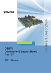
TDC Development Support Board for Siemens Wireless Modules
Introduction
The TDC Development Support Board (DSB) is intended to assist engineers and designers in developing and
evaluating Siemens Wireless modules.
The board supports a number of modules from Siemens, covering GSM, GPS, GPRS, EDGE and 3GSM (HSDPA)
technologies. The board is available only as part of a kit (TDCDSB-NM-ISSUE-3), which includes:
z Software, documentation & utilities CD
z Plastic mounting feet (4)
z G70 12V Power supply
z G60-ML Mains cable
z Antennas (1 x dual band whip, 1 x GSM/GPS combi)
Please specify the module you need when ordering the development board kit.
Although not currently illustrated, the board is supplied with a bracket that mounts on the two centre mounting
holes, and carries a UFL to FME connector for GSM operation, and UFL to SMA for GPS.
UNDER NO CONDITIONS MUST MORE THAN
ONE MODULE BE FITTED at the same time. Damage will occur to both the modules and the board.
The board will only support one module at a time.
Last update - 17th April 2008
TDC Development Support Board for Siemens Wireless Modules
Quickstart
Not much to say here, apart from checking that the jumpers are fitted in accordance with the settings in the overview section for default operation.
Make sure the board is on a clutter-free area so that the back of the board does not short out on anything and connect the serial cable to a suitable terminal or terminal emulation program. The
recommended initial data rate is 115,200bps, N parity, eight data bits and 1 stop bit. Switch off hardware handshaking at this stage.
Connect power and the serial cable to J5 (serial port 0). Switch on the unit by pressing the IGN switch for about a second - the Module OFF LED should switch off, and the SYNC LED should
start flashing. You don't need a SIM fitted at this stage, or even an antenna, but if you do fit them, then the SYNC LED should start to flash with a short flash once the module has registered to
the network.
Open the serial port, and send the characters 'ATI' plus carriage return to the DSB. You should see a message identifying the module returned. If not, then check the connections or check that
you are communicating with the right modem! - a common mistake is to find that your terminal connection is to a modem already installed inside the computer being used.
Last update - 10th May 2007
TDC Development Support Board for Siemens Wireless Modules
Overview
This board is a platform for engineers to develop GSM/GPRS, EDGE, 3G, or combined GSM/GPRS/GPS tracking products using Siemens modem modules. The platform can be powered by either
the supplied power supply or a 9 - 15V bench supply via the 4mm sockets, and has all of the most commonly used interfaces available including 2 x RS232 ports, USB, Audio, I2C and SPI. The
second serial port can easily be configured as a null modem connection using a simple slider switch making it ideal for interfacing GPS receivers, data loggers, etc. For those interested in the
power supply side of things a battery charging circuit is provided along with a fairly flexible power supply circuit which allows for a certain amount of experimentation including the use of super
caps.
TDC's development board has been put together with the engineer in mind and has several useful test points, jumper connectors, and LEDs to aid the design/evaluation process. In addition to
these features every single pin of the module can be accessed directly via an array of pin headers wired to mimic their surface mount counterparts. To make it easy to find the signals required
TDC have included as many useful labels onto the board as possible and provide full circuit diagrams.
There are three connectors fitted to this board to support the latest range of Siemens modules.
z 80 way Molex connector to support TC63, TC65, MC75, XT65, and XT75
z 50 way Hirose connector (J11) to support HC15 and HC25
z 50 way Hirose connector (J15) to support MC55i
Connectors
Connector Description
Links
Description
Factory
setting
LK1
Disconnect power to the module
Fitted
4mm Banana plug power input, negative
LK2
3V3_4V5 Power shutdown
Not connected
J4
Battery connector
LK3
Isolate reservoir capacitor
Fitted
J5
Serial port 0 / ASC 0
LK4
Bypass RV1
Not connected
Serial port 1 / ASC 1
LK5
Fast Charge
Not connected
J7
USB B connector
LK6
DTR Serial Port 0
Fitted
J8
Sim holder
LK7
SHDNn
Not fitted
J9
0.1" SIL breakout connector, replicating J8
LK8
ONLINEn
Fitted
J10
RJ11 connector for handset
LK9
ONLINE1n
Fitted
J11
50 way Hirose DF12 connector for HC15 or HC25 modems
LK10
SHDN1n
Not fitted
J12
0.1" DIL breakout connector, replicating J11
LK11
USB POWER
Not fitted
J13
80 way Molex connector for TC63, TC65, MC75, AC75, XT65, XT75 modems
LK12
CCIN
Fitted
J14
0.1" DIL breakout connector, replicating J13
LK13
IGTN
Not connected
50 way Hirose DF12 connector for MC55i
LK14
E-OFF
Not fitted
LK15
VCHARGE
Fitted
J1
4mm Jack plug, 9-15 volt input, positive on centre conductor
J2
4mm Banana plug power input, positive, 9-15 volts
J3
J6
J15
Link
Switches
LK16
Audio power selection
Fitted across pins 1 & 2
LK17
Chargegate
Fitted
Switch Description
'Fitted' = jumper fitted and shorting pins, 'Not connected' = jumper supplied, but not shorting
pins, 'Not fitted' = no jumper supplied.
SW1
Battery disconnect
SW2
DTE/DCE select (null modem) for Serial port 1 / ASC 1
SW3
Ignition (manual modem switch on)
SW4
Emergency off
Test Points
Ref Description
TP1 5V reference
TP2 GND reference
TP3 3V3_4V5 output from regulator
TP4 Super cap / 3V3_4V5 reference point
TP5 GND reference
TP6 3V output from regulator
TP7 VCHARGE reference
TP8 GND reference
TP9 USB +V
All of the connectors, switches and links are described in detail elsewhere via the hyperlinks.
Board dimensions : 135mm x 178mm x 30mm.
Current consumption : Typical <200mA, charging 400mA (typical), online 900mA (maximum, dependent on module used) - preliminary figures, awaiting characterisation.
Power supply 9-15V DC, power supply should be capable of 1A continuous.
Mounting holes - 3mm diameter.
Please note that this photograph is an early version, and slightly different to the shipped version.
TDC Development Support Board for Siemens Wireless Modules
Connectors
J1 - 4mm Main power
Pin
J10 - Handset, RJ11
Description
Centre Positive power input, 9-15V
Pin Description
Outer Negative power input
1
MIC N
2
EAR N
3
EAR P
4
MIC P
J2 - 4mm banana plug main power
Pin
Description
Main (Red) Positive power input, 9-15V
J3 - 4mm banana plug main power
Pin
Description
Main (Black) Positive power input, 0V / GND
J4 - Battery Connector
Pin
Description
GND Ground connection
TEMP NTC input from battery
BAT+ Positive connection
Push down on the tabs to insert battery terminal wires.
J11 - 50 Way Hirose
Connector
To fit Siemens HC15 or HC25 modems. Please see Siemens documentation for details of pinout.
DO NOT FIT A MODULE TO J13 IF A MODULE IS FITTED TO J11 OR J15.
J12 - 0.1" DIL Breakout Connector
Pin Description Description Pin
1
CCLK
2
CCVCC
MICP 49
3
CCIO
MICN 48
4
CCRST
EPP 47
5
CCIN
EPN 46
6
CCGND
7
SDCC_D2
Please note that only battery types specified by Siemens must be used. 8
Batteries without protection circuits must NOT be used.
9
J5 - Serial port 0 / ASC0
VMIC 50
SDCC_D0
SDCC_CLK
10 GND
AGND 45
SDCC_D3 44
SDCC_D1 43
SDCC_CMD 42
IGT 41
11 PWR_IND
EMERG_OFF 40
12 STATUS0
APP_CTRL0 39
13 STATUS1
RSV38 38
Pin Description
14 USBVCC
1
DCD - Data Carrier Detect
15 USBDP
RCV36 36
2
RXD - Received Data
16 USBDN
APP_CTRL2 35
3
TXD - Transmit Data
17 USBID
4
DTR - Data Terminal Ready
18 VDDLP
RSV33 33
5
GND
19 RSV19
HOST_WU 32
6
DSR - Data Set Ready
20 RSV20
VEXT 31
7
RTS - Request To Send
21 GND21
BATT30 30
8
CTS - Clear To Send
22 GND22
BATT29 29
9
RING - Ring Detect
23 GND23
BATT28 28
24 GND24
BATT27 27
25 GND25
BATT26 26
J6 - Serial port 1 / ASC1
Pin Description
1
NC - No connect
2
RXD - Received Data
3
TXD - Transmit Data
4
NC - No connect
5
GND
6
NC - No connect
7
RTS - Request To Send
8
CTS - Clear To Send
9
NC - No connect
J7 - USB B Jack
Pin Description
1
USBVCC
2
USBDN
3
USBDP
4
GND
J8 - SIM Card Holder
Pin Description
1
VCC
2
RESET
APP_CTRL1 37
DEV_WU 34
J13 - 80 Way Molex Connector
To fit Siemens TC63, TC65, MC75, AC75, XT65 or XT75 modems. Please see Siemens
documentation for details of pinout.
DO NOT FIT A MODULE TO J11 IF A MODULE IS FITTED TO J13 OR J15.
J14 - 0.1" DIL Breakout Connector for J13
Pin Description
Description Pin
1
GND1
2
ADC1_IN
DAC_OUT 79
3
ADC2_IN
PWR_IND 78
4
GND4
RSV77 77
5
GPIO10
GPIO9 76
6
GPIO8
SPICS 75
7
SPID1
GPIO4 74
8
GPIO7
GPIO3 73
9
GPIO6
GPIO2 72
10 GPIO5
11 I2CCLK / SCLK (MC55i)
GND80 80
GPIO1 71
I2CDAT 70
12 VUSB_IN
USB_DP 69
13 DAI5
USB_DN 68
14 ISENSE
VSENSE 67
15 DAI6
VMIC 66
3
CLOCK
16 CCCLK
4
GND
17 CCVCC
EPP2 64
5
VPP
18 CCIO
EPP1 63
6
DATA
19 CCRST
J9 - SIM Card Breakout
EPN2 65
EPN1 62
20 CCIN
NICN2 61
21 CCGND
MICP2 60
22 DAI4
MICP1 59
23 DAI3 / RXDDAI (MC55i)
MICN1 58
Pin Description
24 DAI2 / TFSDAI (MC55i)
AGND 57
1
CCVCC
25 DAI1 / TXDDAI (MC55i)
IGT 56
2
CCRST
26 DAI0 / RFSDAI (MC55i)
EMERG_RST 55
3
CCCLK
27 BATT_TEMP
DCD0 54
4
CCGND
28 SYNC
CTS1 53
5
CCGND
29 RXD1
CTS0 52
6
CCIO
30 RXD0
RTS1 51
7
CCGND
31 TXD1
DTR0 50
8
CCIN
32 TXD0
RTS0 49
33 VDDLP
DSR0 48
34 VCHARGE / POWER (MC55i)
RING0 47
35 CHARGEGATE / CHARGE (MC55i) VEXT_80 / VDD (MC55i) 46
36 GND36
BATT45 45
37 GND37
BATT44 44
38 GND38
BATT43 43
39 GND39
BATT42 42
40 GND40
BATT41 41
J15 - 50 Way Hirose Connector
To fit Siemens MC55i modules. Please see Siemens documentation for deatils of the pinout.
The signals for this connector are also available on J14 (see above table for details).
DO NOT FIT A MODULE TO J15 IF A MODULE IS ALREADY FITTED TO
J11 OR J13.
Last update - 17th April 2008
TDC Development Support Board for Siemens Wireless Modules
Switches
SW1 - 3V3_4V5 / VBATT
When in the 3V3_4V5 position the module will be powered by the main power source and the BAT+ terminal of the battery connector will be
open circuit. In the VBATT position the modem is either battery powered or in battery charge mode depending upon whether or not the link on
the VCHARGE line is connected (LK?).
SW2 - DTE / DCE
With the switch positioned to the top of the board, Serial Port 1 / ASC1 is a DCE. In the lower position, DTE operation is selected. This mode
will be useful if you are connecting to another modem device (such as serial to WiFi or GPS unit for example) when controlling them from Java
code on the module.
SW3 - IGTN
The module can be manually switched on with a momentary operation of this switch.
SW4 - E-OFF
To operate an 'Emergency Off' operation, this switch can be pressed. Please note that for correct operation of the modules, they should be switched off using the AT^SMSO command. This deregisters the module in an orderly and controlled fashion with the network. Using E-OFF or simply disconnecting main power should be avoided.
Last update -5th February 2007
TDC Development Support Board for Siemens Wireless Modules
Links
LK1 - Disconnect power to the module
When fitted, this link connects the power supply derived from the DC input to the module. Breaking this link allows users to insert an ammeter
into the circuit for a more realistic measure of the power being drawn by the modem.
This link also allows the evaluation of a 'super' capacitor. By inserting a resistance at this point to mimic a weaker power supply the system
designer can evaluate the capacitor's ability to supply the large gulps of current taken during a GSM/GPRS transmit burst. To aid testing the
voltage on this power supply line is adjustable using RV1 (2.8 to 4.5V).
LK2 - 3V3_4V5 Power shutdown
When fitted, this link will turn off the regulator responsible for supplying power to the module from the main DC input.
LK3 - Isolate the reservoir capacitor
Removing this link will isolate the super capacitor or large electrolytic capacitors (depending on what is fitted) from the circuit.
LK4 - Bypass RV1
When fitted this link bypasses the variable resistance RV1 giving a fixed supply to the module of 4.5V. With RV1 enabled the supply to the module can be varied between 2.8V to 4.5V.
LK5 - Fast Charge
When charging a battery the maximum current limit can be changed from 500mA to 1A by fitting LK5.
LK6 - DTR disconnect, Serial port 0
When fitted, this link connects DTR to the modem, allowing the modem to power up via the serial port.
LK7 - SHDNn
When fitted, this link will disable Serial Port 0, saving power and allowing other serial devices to be connected to the breakout connectors without conflict.
LK8 - ONLINEn
When fitted, the output of Serial Port 0 is switched off after 100µS of inactivity, therefore saving power. When not fitted, the serial port is active all the time.
LK9 - ONLINE1n
When fitted, the output of Serial Port 1 is switched off after 100µS of inactivity, therefore saving power. When not fitted, the serial port is active all the time.
LK10 - SHDN1n
When fitted, this link will disable Serial Port 1, saving power and allowing other serial devices to be connected to the breakout connectors without conflict.
LK11 - USB Power
When fitted, supplies 5V from the board onto the USB port. Most host devices will supply their own voltage to this pin, so use this pin with care, as power supply conflicts may occur if the
jumper is fitted.
LK12 - CCIN
When fitted, this link simulates the CCIN (sim detect) feature that is present on some SIM card holders.
LK13 - IGTN
Shorts the ignition input to the modem, or allows for an external switch to be fitted.
LK14 - E-OFF
Shorts the emergency off switch, but allows for an external switch to be fitted.
LK15 - VCHARGE
When fitted this link connects 5V to the VCHARGE pin on the module. This tells the module that a charger is connected so if a battery with less than full capacity is connected the charging
process will commence.
LK16 - Module Audio Selection
When using the MC55i to make audio calls LK16 must be fitted such that it connects pins 2 & 3 together. For all other modules fit the link so that pins 1 & 2 are connected.
LK17 - Chargegate
This link can be used to disconnect the Chargegate signal which controls the battery charging functionality.
Last update - 17th April 2008
TDC Development Support Board for Siemens Wireless Modules
Indicators
I2C / SPI Port
Sync
LED
Colour Description
SPI CS
Green
I2C CLK / SPI CLK Green
I2C or SPI Clock
I2C DAT / SPI DO Green
I2C Data or SPI Data Out
SPI DI
SPI Data In
Green
Serial Port 0
LED Colour Description
RING Red
CTS
RTS
Flashes in accordance with
SYNC output of modem - see
AT^SYNC command
SYNC Red
Power
LED Colour Description
PWR Green
Ring Indicator
Orange Clear To Send
DCD Red
LED Colour Description
SPI Chip Select
Data Carrier Detect
Indicates main power is
applied to the board
HC15 / HC25 Status
Orange Request To Send
TXD Green
Transmit data
LED
DSR Red
Data Set Ready
STATUS 0 Green
GSM Network registration status
RXD Green
Receive Data
STATUS 1 Green
UMTS Network registration status
Serial Port 1
Colour Description
Modem Off
LED Colour Description
LED
CTS Orange Clear To Send
MODEM OFF Green
Colour Description
Illuminates when modem is off
RTS Orange Request To Send
TXD Green
Transmit Data
RXD Green
Receive Data
Last update - 5th February 2007