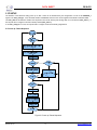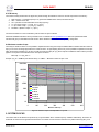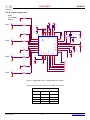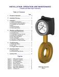
1
DATA SHEET QF4A512 4-Channel Programmable Signal Converter (PSC) APPLICATIONS • • • • • • FEATURES Wireless Sensor Networks • 4 Channel Analog 16-bit Programmable A/D Converter • Differential or Single Ended Inputs Machine Monitoring • 4 Programmable (1x, 2x, 4x, 8x) Gain Amplifiers Smart Sensors • Anti-Aliasing Filter Per Channel, 3rd Order Bessel Industrial Control Medical Monitoring and Diagnostics • Analog DC – 900kHz, up to 2Msps Sampling rate Homeland Security • Internal Precision Voltage Reference DESCRIPTION • 4 Individual Programmable 512-tap Digital FIR Filters The QF4A512 Programmable Signal Converter is a 4-channel, signal conditioner and signal converter. Each channel can be individually programmed for the gain, anti-aliasing filter cutoff frequency, A-to-D sampling frequency, and unique filter requirements. This is accomplished with 4 separate highprecision 512-tap FIR filters. • SPI Port Interface Quickfilter Pro software has been created for rapid device configuration and filter design at performance levels unattainable with analog components. • 3.3V Digital I/O, 5 Volt Tolerant • 32-Pin LQFP Package • Industrial Temp -40C to +85C • 4K Byte EEPROM for filter coefficient, chip configuration and calibration. ORDERING INFORMATION 128 bytes of EEPROM User Data Space 384 Bit Masks for IEEE 1451.4 TEDS on 4 Channels Device Package QF4A512-LQ--T QF4A512-LQ--B 32-Pin LQFP - Tape & Reel (Reel qty 1000) - Trays QUICKFILTER DEVELOPMENT KIT QF4A512-DK Development Kit (QF4A512-DK) Quickfilter Pro Windows®-based Software for Rapid Filter Design and IC Configuration In-System Programmability (ISP) trough SPI Port Evaluation board for verification of device performance EEPROM 512-Tap Digital Filters Anti-Alias Filters AIN1+ + AIN1- - AIN2+ + PGA AIN2- - AIN3+ + A M U X PGA AIN3- - AIN4+ + RAM FIR PGA 12 to 16 Bit Converter ADC SCL FIR D E M U X SDI SPI FIR DRDY /SEL Vref FIR PGA AIN4- SDO /CS ADC Clock Cutoff Frequency Control AVDD AGND DVDD DGND System Clocks /RST PLL XIN XOUT Functional Block Diagram PRODUCTION DATA is current as of the publication date. Production processing does not necessarily include testing of all parameters. Product conformance is per Quickfilter’s standard warranty. Filter Design Screen Rev D4, Dec 07 http://www.quickfiltertech.com/ DATA SHEET QF4A512 TABLE OF CONTENTS 1. SPECIFICATIONS .............................................................................................................................................................. 4 1.1 ABSOLUTE MAXIMUM RATINGS ........................................................................................................................................ 4 1.2 PACKAGE ASSEMBLY ...................................................................................................................................................... 4 1.3 RECOMMENDED OPERATING CONDITIONS ........................................................................................................................ 4 1.4 ELECTRICAL CHARACTERISTICS ...................................................................................................................................... 5 1.5 TIMING REQUIREMENTS ................................................................................................................................................... 7 1.6 TYPICAL PERFORMANCE CHARACTERISTICS .................................................................................................................... 8 2. PINOUT AND PIN DESCRIPTIONS ................................................................................................................................... 9 2.1 PINOUT ........................................................................................................................................................................... 9 2.2 PIN DESCRIPTIONS .......................................................................................................................................................... 9 3. GENERAL DESCRIPTION ............................................................................................................................................... 11 3.1 ANALOG FRONT END (AFE) .......................................................................................................................................... 11 3.2 ANALOG TO DIGITAL CONVERTER (ADC) ....................................................................................................................... 11 3.3 FINITE IMPULSE RESPONSE FILTER (FIR) ....................................................................................................................... 12 3.4 SERIAL INTERFACE - SERIAL PERIPHERAL INTERFACE (SPI) ........................................................................................... 12 3.5 STARTUP MODES .......................................................................................................................................................... 12 3.6 MEMORY ....................................................................................................................................................................... 12 4. SOFTWARE ...................................................................................................................................................................... 13 4.1 DEVICE CONFIGURATION ............................................................................................................................................... 13 4.2 QUICKFILTER DEVELOPMENT KIT (QF4A512DK) ........................................................................................................... 13 4.3 IN-CIRCUIT (RE)CONFIGURATION .................................................................................................................................... 13 5. STARTUP ......................................................................................................................................................................... 14 5.1 POWER UP / RESET SEQUENCE ...................................................................................................................................... 14 5.2 EXTENDED INITIALIZATION ............................................................................................................................................. 15 5.3 CALIBRATION ................................................................................................................................................................ 16 6. ANALOG FRONT END (AFE) .......................................................................................................................................... 17 6.1 CONFIGURABLE PARAMETERS ....................................................................................................................................... 17 6.2 CHOPPER-STABILIZED AMPLIFIER .................................................................................................................................. 17 6.3 PROGRAMMABLE GAIN AMPLIFIER (PGA) ...................................................................................................................... 17 6.4 INPUT VOLTAGE LEVELS................................................................................................................................................ 18 6.5 ANTI-ALIASING FILTER (AAF) ....................................................................................................................................... 18 6.6 ENABLING CHANNELS ................................................................................................................................................... 18 7. ANALOG TO DIGITAL CONVERTER ............................................................................................................................. 19 7.1 OVERVIEW .................................................................................................................................................................... 19 7.2 SAMPLING RATES / ENOB ............................................................................................................................................ 19 7.3 AGGREGATE BANDWIDTH .............................................................................................................................................. 19 7.4 SERIAL INTERFACE........................................................................................................................................................ 20 7.5 DATA FORMAT .............................................................................................................................................................. 20 7.6 ANALOG MUX ............................................................................................................................................................... 20 7.7 GAIN AND OFFSET CALIBRATION ................................................................................................................................... 20 7.8 FACTORY CALIBRATION................................................................................................................................................. 20 7.9 USER (SYSTEM LEVEL) CALIBRATION ............................................................................................................................. 21 8. FIR FILTERS .................................................................................................................................................................... 22 8.1 FIR OVERVIEW ............................................................................................................................................................. 22 8.2 FIR MEMORY LOCATIONS .............................................................................................................................................. 22 8.3 FIR LATENCY................................................................................................................................................................ 23 8.4 MAXIMUM NUMBER OF TAPS ........................................................................................................................................... 23 Rev D4, Dec 07 2 www.quickfiltertech.com DATA SHEET QF4A512 9. SYSTEM CLOCKS ........................................................................................................................................................... 23 9.1 PLL CLOCK .................................................................................................................................................................. 24 9.2 SYSTEM CLOCK ............................................................................................................................................................ 24 9.3 ADC CLOCK ................................................................................................................................................................. 24 9.4 EE CLOCK .................................................................................................................................................................... 24 10. SERIAL INTERFACE ..................................................................................................................................................... 24 10.1 MODES OF OPERATION................................................................................................................................................ 24 10.2 CONFIGURE MODE ...................................................................................................................................................... 25 10.3 RUN MODE ................................................................................................................................................................. 27 10.4 SENDING COMMANDS IN RUN MODE ............................................................................................................................ 29 11. EEPROM ......................................................................................................................................................................... 31 11.1 OVERVIEW .................................................................................................................................................................. 31 11.2 EEPROM TRANSFER PROCEDURES ............................................................................................................................ 31 11.3 CALIBRATION DATA .................................................................................................................................................... 32 11.4 USER MEMORY ........................................................................................................................................................... 32 12. CONTROL REGISTERS................................................................................................................................................. 33 12.1 OVERVIEW .................................................................................................................................................................. 33 12.2 HIGH-LEVEL REGISTERS .............................................................................................................................................. 34 12.3 EEPROM STARTUP REGISTERS.................................................................................................................................. 35 12.4 RUN AND STATUS REGISTERS ..................................................................................................................................... 37 12.5 GLOBAL CONFIGURATION REGISTERS.......................................................................................................................... 40 12.6 GLOBAL MAINTENANCE REGISTERS............................................................................................................................. 43 12.7 CHANNEL-SPECIFIC REGISTERS ................................................................................................................................... 44 12.8 GLOBAL MAINTENANCE 2 REGISTERS .......................................................................................................................... 53 12.9 FIR COEFFICIENT AND RAM REGISTERS ...................................................................................................................... 54 12.10 REGISTER LISTING .................................................................................................................................................... 59 13. APPLICATION CIRCUITS .............................................................................................................................................. 61 13.1 AC COUPLED, SINGLE-ENDED ..................................................................................................................................... 61 13.2 DC COUPLED, SINGLE-ENDED ...................................................................................................................................... 62 13.3 AC COUPLED, DIFFERENTIAL ....................................................................................................................................... 63 13.4 DC COUPLED, DIFFERENTIAL ....................................................................................................................................... 64 14. PACKAGING INFORMATION ........................................................................................................................................ 65 LIST OF FIGURES ................................................................................................................................................................ 66 LIST OF TABLES .................................................................................................................................................................. 66 Rev D4, Dec 07 3 www.quickfiltertech.com DATA SHEET QF4A512 1. SPECIFICATIONS 1.1 Absolute Maximum Ratings Stresses above those listed under Absolute Maximum Ratings can cause permanent device failure. Functionality at or above these limits is not implied. Exposure to absolute maximum ratings for extended periods may affect device reliability. Parameter Min Max Units Storage Temperature -60 125 ºC Supply Voltage, VDD18 to DGND -0.2V 2.2V V Supply Voltage, VDD33 with respect to DGND -0.2V 4.0V V Digital Input Voltage with respect to DGND -0.3 7 V Analog Input Voltage with respect to AGND -0.3 VDD33 + 0.3 V ESD Immunity (Human Body Model, JESD222 Class 1C)) 1000 V This integrated circuit can be damaged by ESD. Quickfilter Technologies recommends that all integrated circuits be handled with appropriate precautions. Failure to observe proper handling and installation procedures can cause damage. 1.2 Package Assembly The QF4A512 is offered in a “green” package (RoHS & no Sb/Br), assembled with enhanced environmentally compatible Pb-free and halide-free materials. The leads possess a matte-tin plating which is compatible with conventional board assembly processes or newer lead-free board assembly processes. The peak soldering temperature should not exceed 260°C during printed circuit board assembly. 1.3 Recommended Operating Conditions Parameter Symbol Min Typ Max Units Supply Voltage 1.8 VDD18 1.6 1.8 2.0 V Supply Voltage 3.3 VDD33 3.0 3.3 3.6 V 0 5.5 V AIN 0.2 2.5 V Clock Frequency f0 5 20 200 MHz Ambient Temperature TA -40 25 85 ºC ADC Clock Rate fADC 100 MHz Digital Input Voltage Analog Input Voltage Note: Quickfilter guarantees the performance of this device over specified ranges by conducting electrical characterization over each range and by conducting a production test with single insertion coupled to periodic sampling. Rev D4, Dec 07 4 www.quickfiltertech.com DATA SHEET QF4A512 1.4 Electrical Characteristics Symbol Parameter (Condition) Min Typ Max Units Note Resolution N NMC Resolution, Nominal 16 Bits No Missing Codes Guaranteed 16 Bits DC Accuracy PSRR Power-supply rejection ratio 54 dB GERR Gain Error (Uncalibrated) 1 VOS DC Offset Error (Uncalibrated) - Chopper Off - Chopper On ±10 VREF Internal Voltage Reference 1.2 V 100 ppm/°C ± 0.01 TCVREF Internal Voltage Reference Drift over temp INL Integral Non-linearity (PGA = x1) DNL Differential Non-linearity (PGA = x1) %FSR 1 mV 1 0.02 %FS 1 LSB 2 AC Accuracy fS = 2kHz fS = 20kHz fS = 200kHz fS = 2MHz 82 81 77 69 dBFS 3 SINAD fS = 2kHz fS = 20kHz fS = 200kHz fS = 2MHz 81 80 76 69 dBFS 3 SFDR Spurious Free Dynamic Range, fS = 2kHz fS = 20kHz fS = 200kHz fS = 2MHz 89 88 88 87 dBc 3 Total Harmonic Distortion, fS = 2kHz fS = 20kHz fS = 200kHz fS = 2MHz -89 -88 -85 -83 dBc 3 fS = 2kHz fS = 20kHz fS = 200kHz fS = 2MHz 13.2 13.0 12.4 11.2 Bits 3 Signal To Noise Ratio, SNR Signal To Noise and Distortion, THD Effective number of bits ENOB Analog Inputs VFSR Input Differential Voltage Range VCM Input Common Mode Voltage Range CMRR 0.2 1.6 2.0 V P-P 1.2 2.5 V Common Mode Rejection Ratio 55 dB CIN Input Capacitance (Single Ended) 5 pF RIN Input Resistance (Single Ended) Rev D4, Dec 07 9.2 5 10.0 10.8 kΩ 4 www.quickfiltertech.com DATA SHEET Differential Input Capacitance QF4A512 10 Differential Input Resistance 4.6 5 pF 5.4 kΩ AV_PB Passband Attenuation (DC to 500 kHz) 0.2 dB GD Group Delay Variation (DC to 500 kHz) 5 % CI AN Channel Isolation, fADC = 50MHz fADC = 100MHz 75 35 Alias Noise Attenuation 4 dBc 45 dB 500 3 Anti-aliasing Filter Cutoff Frequency, aaf_freq=0 aaf_freq=1 kHz MHz Supply Current & Power Dissipation 1.8V Supply Operating Current IDD18 3.3V Supply Operating Current IDD33 PDD - fS = 1kHz (four channels) - fS = 100kHz (four channels) - fS = 2MHz (single channel) - Standby - Power down 98 129 147 1.1 0.5 mA 5 - fS = 1kHz (four channels) - fS = 100kHz (four channels) - fS = 2MHz (single channel) - Standby - Power Down 17 17 4.3 0.6 0.2 mA 5 87 4 1.6 mW 5 Power Dissipation, Active - Single channel, fS = 100kHz - Standby - Power Down Digital Inputs (SCLK, SDI, /CS, /RST) † VIH High-level Input Voltage, DVDD33 = 3.6V 2 5.5 V VIL Low-level Input Voltage, DVDD33 = 3.0V -0.3 0.8 V IIN Input (leakage) current (SCLK, SDI) 2.1 nA RIN Pull-up Resistance (/CS, /RST) Pull-down Resistance (DRDY) 31 kΩ CIN Input Capacitance Digital Input (XIN) 10 pF † VIH High-level Input Voltage, DVDD18 = 2.0V 1.4 5.5 V VIL Low-level Input Voltage, DVDD18 = 1.6V 0 0.4 V IIN Input (leakage) current CIN Input Capacitance Digital Outputs (SDO, DRDY/SEL) 1.9 nA 10 pF † VOH High-level Output Voltage, DVDD33 = 3.0V, IOH = -100uA VOL Low-level Output Voltage, DVDD33 = 3.0V, IOL = 100uA 0.2 V CO Output Capacitance 10 pF CL Load Capacitance 30 pF Digital Output (XOUT) Rev D4, Dec 07 2.8 V † 6 www.quickfiltertech.com DATA SHEET QF4A512 VOH High-level Output Voltage, DVDD18 = 1.6V, IOH = -100uA 1.4 V VOL Low-level Output Voltage, DVDD18 = 3.0V, IOL = 100uA 0.2 V CO Output Capacitance 10 pF CL Load Capacitance 20 pF 1. System calibration will reduce these errors to below the noise level. 2. System calibration at any temperature will eliminate this error. 3. Programmable Gain Amplifier set at a gain of x1, fIN = fs / 25 4. Input resistance may vary as much as +/-26% without calibration. See gain and offset calibration. 5. Standby is with all channels inactive, and analog front end turned off. Power down is when the oscillator/PLL is turned off. † The digital input and output pins are 5V-tolerant. Inputs may be driven with 5V signals, outputs can be connected via pull-ups to 5V levels. 1.5 Timing Requirements Parameter Min Max Units 5 200 MHz Serial Port Clock Frequency, fSCLK (Run and Configure Modes) 40 MHz Serial Port Clock Frequency, fEE (EEPROM Mode) 5 MHz 200 MHz Input Clock Frequency, f0 PLL Clock Frequency, PLL_CLK 20 Chip select low pulse width 2/SYS_CLK SYS_CLK frequency (User filters, sampling rates) ns (((NTAPS + 1)/2)+1)*fS PLL_CLK 6, 9 103* fS PLL_CLK 7, 9 3*SCLK/16 SCLK/(8*N) PLL_CLK 8, 9 SYS_CLK frequency (Fixed G and H filters) SYS_CLK frequency (relative to SCLK) Note - 16-bit output - 24-bit output Setup time, Chip Select (/CS) low to SCLK↑ 5 ns Setup time, SDI before SCLK↑ 5 ns Hold time, SDI after SCLK↑ 5 ns 6. fS is the sampling rate for any given channel and NTAPS is the number of taps used in the associated FIR. The highest value of the expression for any active channel defines the minimum frequency for SYS_CLK. 7. This parameter is derived in similar fashion to the previous one and is determined by the fixed number of taps used in the G and H filters. 8. This limit is caused by the requirement for DRDY to be cleared before /CS returns to a high level after a data transfer. Two SYS_CLKS are required to clear DRDY this must occur before the data transfer is completed. N is the number of channels active in the output data. 9. All three of the minimum conditions must be satisfied for correct device operation. Rev D4, Dec 07 7 www.quickfiltertech.com DATA SHEET QF4A512 1.6 Typical Performance Characteristics Default Conditions: TA = 25 C, VDD18 = 1.8V, VDD33 = 3.3V, unless otherwise noted. ENOB vs. Data Rate SINAD vs. Data Rate 14 90 13 12 SINAD (dB) ENOB (bits) 80 11 70 60 10 Chop OFF, 1.8V/3.3V Chop OFF, 1.8V/3.3V Chop ON, 1.8V/3.3V Chop ON, 1.8V/3.3V 9 50 1 10 Data Rate (kSPS) 100 1000 1 10 SFDR vs. Data Rate Data Rate (kSPS) 100 1000 SNR vs. Data Rate 90 100 90 80 SNR (dB) SFDR (dB) 80 70 70 60 60 Chop OFF, 1.8V/3.3V Chop OFF, 1.8V/3.3V Chop ON, 1.8V/3.3V Chop ON, 1.8V/3.3V 50 50 1 10 100 1000 1 10 Data Rate (kSPS) 100 1000 Data Rate (kSPS) Channel Isolation vs. ADC Frequency THD vs. Data Rate 100 -50 Chop OFF, 1.8V/3.3V Chop ON, 1.8V/3.3V 80 Minimum CI (dB) THD (dB) -60 -70 -80 60 40 20 -90 0 -100 1 10 100 10 1000 Rev D4, Dec 07 30 50 70 90 ADC Frequency (MHz) Data Rate (kSPS) 8 www.quickfiltertech.com DATA SHEET QF4A512 Supply Current vs Number of Channels (3.3V) Supply Current vs Number of Channels (1.8V) 20 160 16 120 Supply Current (mA) Supply Current (mA) 80 12 8 40 4 1ksps 100ksps 2Msps 0 0 2 1 3 4 1 2 3 4 Number of Active Channels Number of Active Channels 2. PINOUT and PIN DESCRIPTIONS 2.1 Pinout AIN1- 1 24 XGND AIN1+ 2 23 XOUT AIN2- 3 22 XIN 21 XVDD18 20 DVDD3 DVDD18 QF4A512 AIN2+ 4 AIN3- 5 AIN3+ 6 19 AIN4- 7 18 DGND AIN4+ 8 17 RST 32 LQFP 2.2 Pin Descriptions Pin # Pin Name Type 1 AIN1- Input Analog Input Channel 1 Differential-, or DC bias input (SE) 2 AIN1+ Input Analog Input Channel 1, Single-Ended or Differential+ (No phase shift) 3 AIN2- Input Analog Input Channel 2 Differential-, or DC bias input (SE) 4 AIN2+ Input Analog Input Channel 2 , Single-Ended or Differential+ (No phase shift) 5 AIN3- Input Analog Input Channel 3 Differential-, or DC bias input (SE) 6 AIN3+ Input Analog Input Channel 3, Single-Ended or Differential+ (No phase shift) 7 AIN4- Input Analog Input Channel 4 Differential-, or DC bias input (SE) 8 AIN4+ Input Analog Input Channel 4, Single-Ended or Differential+ (No phase shift) Rev D4, Dec 07 Description 9 www.quickfiltertech.com DATA SHEET 9 DVDD18 Power +1.8V DC Power (Digital) 10 DGND Ground Digital Ground 11 DGND Ground Digital Ground 12 /CS Input 13 DRDY/SEL Input/Output Chip Select from SPI Bus (Low logic selects chip). Internal pull-up. High when new data is ready, if pulled high accesses EEPROM direct. Internal pull-down. 14 SDO Output 15 SDI Input SPI Serial Data Input 16 SCLK Input SPI Clock (Maximum 40 MHz) 17 /RST Input Chip RESET (Low logic resets chip). Internal pull-up. 18 DGND Ground Digital Ground 19 DVDD18 Power +1.8V DC Power (Digital) 20 DVDD33 Power +3.3V DC Power (Digital) 21 XVDD18 Power Filtered +1.8V DC Power for Internal Oscillator 22 XIN Input 23 XOUT Output Crystal connection 24 XGND Ground Ground for Internal Oscillator 25 PGND Ground Ground for Phase Lock Loop 26 PVDD18 Power +1.8V DC Filtered Power for Phase Lock Loop 27 AGND Ground Analog Ground 28 AVDD18 Power +1.8V DC Power (Analog) 29 AVDD18 Power +1.8V DC Power (Analog) 30 AGND Ground Analog Ground 31 AGND Ground Analog Ground 32 AVDD33 Power +3.3V DC Power (Analog) Rev D4, Dec 07 QF4A512 SPI Serial Data Output Crystal connection or external clock input (5-200 MHz) 10 www.quickfiltertech.com DATA SHEET QF4A512 3. GENERAL DESCRIPTION Figure 1. Functional Block Diagram 3.1 Analog Front End (AFE) The AFE consists of a Programmable Gain Amplifier (PGA), a chopper-stabilized amplifier and an Anti-Aliasing Filter. Programmable Gain Amplifier (PGA) The PGA can be set at gains of 1X, 2X, 4X, and 8X. The input impedance of the PGA is 10kΩ on both the positive and negative inputs. The PGA can be configured as either single ended or differential and can receive inputs of up to 2.0V p-p directly. With a single scaling resistor in each channel, two if configured differentially, the PGA can receive signals of up to +/- 10Vp-p or higher. Chopper-stabilized Amplifier (not shown in diagram) This circuit minimizes correlated (1/f) noise and dc offset within the chip. For sampling rates less than 200kHz this circuit will maximize signal-to-noise performance, and hence SINAD and ENOB. (see Section 6.2) Anti-Aliasing Filter (AAF) The Anti-Aliasing Filter is designed to reject frequencies that are higher than the band of interest. If those frequencies are sent to the ADC, they can alias back into the band of interest and can cause erroneous readings to result. The AAF is a 3rd order Bessel function (linear phase) and is set to the appropriate cut-off frequency based on the filter design that is implemented. The AAF has two available cut off frequencies, 500kHz and 3MHz. 3.2 Analog to Digital Converter (ADC) The ADC has a pipeline architecture that is 12 bits in hardware and runs at up to 100Msps. Resolutions of up to 16 bits are achieved by oversampling the input and averaging the resultant conversions. During Chip Configuration and Filter Design, the exact sampling speed of the ADC is determined (based on the highest sampling rate required for any one of the four channels). Not shown in the block diagram are the following sub-blocks which handle decimation/down-conversion of the oversampled data: CIC (Cascaded Integrator Comb Filters) The purpose of the CIC filter is the integration of 16 bits, and adjustment of the proper sample rate through decimation. The digitized signal is then processed in the CIH (Cascaded Integrator Halfband Filters) CIH (Cascaded Integrator Halfband Filters) Rev D4, Dec 07 11 www.quickfiltertech.com DATA SHEET QF4A512 The purpose of the CIH stage is droop recovery to compensate for the frequency response of the CIC filter. After moving through the CIH, the signals are sent into the FIR (Finite Impulse Response Filter) for user filtering. 3.3 Finite Impulse Response filter (FIR) The four FIR filters consist of 512 taps each and are individually programmable. A different filter design may be implemented in each of the 4 filters and may include lowpass, notched lowpass, highpass, bandpass, dual bandpass, bandstop, and dual bandstop. Currently available filter algorithms include Parks-McClellan and Windowed Sinc. 3.4 Serial Interface - Serial Peripheral Interface (SPI) The serial interface is fully compatible with a standard SPI bus. The serial bus on the QF4A512 is capable of running at up to 40 MHz, although it may be run at much lower speeds. The QF4A512 operates in a SLAVE mode. Two main modes of operation are used by the bus: “Configure” mode is used to setup and program the QF4A512 Coefficient RAMs and control registers. Read access to the data RAMs is also available. “Run” mode provides up to 4 channels of 16-bit multiplexed data out the SPI port. The format is 24-bit (New Data Flag + Over Flow Info + Channel ID + 16-bits of data) multiplexed data. The chip will arbitrate between the incoming channels from the FIRs by monitoring each channel's internal data ready signal. If new data for a given channel is ready in time, it will be inserted on the serial output stream at the appropriate place for that channel and the new data flag will be set in the header. Otherwise the old data will remain in the time slot and the new data flag will not be set. The highest channel sample rate is used as the data rate output for a Data Ready signal, which can be used to maximize bus throughput. 3.5 Startup Modes The behavior of the QF4A512 during power up or after a reset can be determined by the configuration of 2 bits in the STARTUP_1 register (07h). The auto_config bit, if set, will initiate transfer of EEPROM contents to the control registers and FIR filter coefficient RAMs. The auto_start bit will determine whether the chip starts in Run mode, filtering and sending data out on the SPI bus (auto_start=1), or the chip will wait in configure mode until manually started (auto_start=0). If the auto_config bit is not set, the chip will wait in configure mode until externally programmed. An Extended Initialization mode is also available to perform sequences of data transfers from EEPROM to chip control registers (See Chapter 5). 3.6 Memory The QF4A512 features on-chip Control Registers, RAM and EEPROM. Important device configuration data and filter coefficients can be copied to EEPROM to provide non-volatility. These data can be copied back from EEPROM when the chip is powered up making it unnecessary to reprogram the device at each power up or reset. RAM / REGISTERS 3FFF 2400 Not Used (no physical memory) EEPROM (Sec 11) Filter Data (Sec 8.2) 0FFF 0F80 Serial Interface Configure Mode 1000 0F00 Not Used 0F00 One to one Mapping Filter Coefficient RAM (Sec 8.2) 0100 Serial Interface Run Mode 0000 User Data (128 bytes) Calibration Data (128 Bytes) Filter Coefficient Data 0100 Control and Status Registers (Sec 12) 0000 Control and Status Data Figure 2. Memory Map Rev D4, Dec 07 12 www.quickfiltertech.com DATA SHEET QF4A512 Within EEPROM, 128 bytes of user space are provided for storing application-specific information. This data could include, for example, Transducer Electronic Data Sheets (TEDS, IEEE P1451.4). The full 14-bit address space can be accessed via the SPI interface in the "Configure" mode. In the "Run" mode only 8-bits of address space can be accessed, which include the command registers and other general configuration registers. 4. SOFTWARE 4.1 Device Configuration Before useful data can be output from the QF4A512 it must first be correctly configured. Configuration parameters include the following: 1. Startup mode. Options include copying configuration parameters and filter coefficients from EEPROM and then immediately running or waiting for an external command. 2. Number of channels to be active. 3. Gain of the PGA for each input channel. 4. Cutoff frequency of the anti-aliasing filter for each channel. 5. Analog to digital converter sampling rate and decimation/down conversion rate for each channel. 6. FIR filter coefficients. 7. Output data format. 4.2 Quickfilter Development Kit (QF4A512-DK) The Development Kit is a complete hardware and software combination which allows for rapid development of the QF4A512 configuration parameters for a specific application. The Quickfilter Pro Design Software tool allows all the necessary parameters to be generated in a quick and user-friendly manner. The user enters the desired characteristics (e.g. sampling rates, type of filter, cut-off frequencies etc.) for each channel and the software generates a configuration file for the device. The configuration file can be immediately downloaded into the QF4A512 on the development board, and the actual hardware device performance can be monitored - either in response to a PC-generated noise source or to a user-applied signal. Device configuration parameters can be further adjusted, if necessary, until the optimum system performance is reached. Once satisfied with the performance the configuration file can be saved for future use, for example to program devices in bulk prior to volume board manufacturing. 4.3 In-circuit (Re)configuration The Quickfilter Pro Design Software is the recommended method to derive the configuration data for the device. However, it may sometimes be desired to verify the configuration written to the device. Or, in certain applications, it may be desired to re-configure the device in circuit from a host MCU, for example to switch channels on/off, change gain values etc. Therefore, more detailed descriptions of device operation and descriptions of various register settings etc. can be found in sections 5 – 12. For most applications the software alone will be sufficient to provide optimum device performance and reference to these sections will be unnecessary. Rev D4, Dec 07 13 www.quickfiltertech.com DATA SHEET QF4A512 5. STARTUP The behavior of the QF4A512 during power up or after a reset can be determined by the configuration of 2 bits in the STARTUP_1 register. The auto_config bit, if set, will initiate transfer of EEPROM contents to the control registers and FIR filter coefficient RAMs. The auto_start bit will determine whether the chip starts in Run mode, filtering and sending data out on the SPI bus (auto_start=1), or the chip will wait in configure mode until manually started (auto_start=0). If the auto_config bit is not set, the chip will wait in configure mode until externally programmed. 5.1 Power up / Reset Sequence Figure 3. Power up / Reset Sequence Rev D4, Dec 07 14 www.quickfiltertech.com DATA SHEET QF4A512 The sequence of events that occurs after a hardware reset is detailed in the preceding diagram. The hardware reset will be applied at power-up or when the external /RST pin is toggled low. If the DRDY pin is held high (for example to write directly to EEPROM) the startup sequence is bypassed. 5.2 Extended Initialization There is an option to perform an Extended Initialization regardless of the setting for auto_config. The Extended Initialization comprises a series of programmable block transfers from the EEPROM to the on-chip registers. To invoke Extended Initialization the alt_startup1 bit must be set in the STARTUP_1 register (07h). This will cause the chip to read the xtnd_init bit in the STARTUP_2 Register (Bit 2, register 08h) to determine if an Extended Initialization will occur. If xtnd_init is set the chip will then read the starting address for the sequence(s) in EEPROM, initseq_addr, from registers IGC_SEQADDR (EBh, ECh). 0xEB CHIP REGISTERS EEPROM initseq_addr seqstop_addr 0xEC seq_eestartaddr seq_sifstartaddr Seq #1 seq_sifendaddr seq_sifstartaddr -> seq_sifendaddr -> seq_eestartaddr seq_sifstartaddr Seq #N seq_sifendaddr seqstop_addr -> seq_eestartaddr -> Figure 4. Extended Initialization Rev D4, Dec 07 15 www.quickfiltertech.com DATA SHEET QF4A512 Note: The value in the IGC_SEQADDR registers can set in two ways. By default, if auto_config is not set it will take a value of F00h – corresponding to the start of User Memory. If auto_config is set it will be written to the value stored in the corresponding EEPROM address. The format for the sequences stored in EEPROM is shown in figure 4. The sequences must be in consecutive memory locations and consist of a series of addresses, each having a 16-bit (i.e 2 byte) value. The first address, seqstop_addr, is simply the ending address for the sequence and points to the byte immediately following the final sequence address. This is then followed by a series of sequences, each comprising three addresses. The first address, seq_eestartaddr, points to the starting address in EEPROM for the block read. The second address, seq_sifstartaddr, points to the destination starting address for where the block data will be written. The third address, seq_sifendaddr, is the destination ending address for the data to be written. This will cause the chip to copy a number of bytes, N, starting at address seq_eestartaddr to a block of registers starting at seq_sifstart_addr and ending at seq_sifendaddr, where seq_sifendaddr = seq_sifstartaddr + N – 1. Once this transfer is complete the chip will move to the next sequence and perform a similar operation for its specified addresses, until it reaches seqstop_addr. At this point the chip will return to the corresponding point in the Power Up / Reset flow as shown in figure 3. 5.3 Calibration One possible use for an Extended Initialization sequence is to transfer calibration values stored in EEPROM to the corresponding gain and offset calibration registers for each channel. For more information see Section 7.7. Rev D4, Dec 07 16 www.quickfiltertech.com DATA SHEET QF4A512 6. ANALOG FRONT END (AFE) 6.1 Configurable parameters The following items are configurable for the AFE: 1. 2. 3. 4. Chopper on or off PGA Gain AAF Cutoff Frequency Channel on or off These settings can all be configured via the Quickfilter Pro software. 6.2 Chopper-stabilized Amplifier Low frequency flicker noise, which is inherent to CMOS devices, limits maximum dynamic range that can be attained solely by oversampling and averaging data from the analog front end (AFE). This flicker noise has a 1/f^n characteristic, which dominates other noise sources at low frequencies of interest. This is in contrast to white noise, with a flat frequency spectrum, which proportionally decreases with oversampling and averaging. Chopper stabilization is a technique that applies modulation to transpose the signal of interest to a higher frequency where there is no flicker noise, and then demodulate it back to the baseband after amplification. Details can be found in the following paper: ‘Circuit Techniques for Reducing the Effects of Op-Amp Imperfections: Autozeroing, Correlated Double Sampling, and Chopper Stabilisation’ By Enz and Temes, Proceedings of the IEEE, November 1996. In the QF4A512, the circuit is chopped at the input (prior to the PGA) and is remodulated back to the baseband after the analog to digital conversion has occurred. Harmonic components of the chopper frequency are subsequently filtered out in the CIC and CIH blocks. The chopper circuit improves the SNR for configurations with data rates 200 kHz and below. Two important settings in the QF4A512 are the chopper frequency and the phase offset between the modulator and demodulator. The chopper frequency is set with a divider whose setting is closely related to the CIC R decimation value. The chopper frequency is derived from the ADC clock and the divider value is stored in the CHPC_DIVn register for each channel. The best setting for the chopper divider is 2 x R x (# of active channels) in most cases. This setting puts the chopper 2nd harmonic frequency in the first null of the CIC filter to most effectively remove it from the final digital signal. While the chopper circuit is effective at signal data rates of 200 kHz and below (down to Hz), the chopper signal itself is most effective at 10 kHz and above, which means the chopper divider should track the CIC R value down only to the point where the chopper frequency would be 10 kHz. For example, for a 4 channel configuration, with the ADC clock running at 50 MHz, and output data rates of 10 kHz and below, the chopper divider should be set no higher than 4E2h (decimal 1250) to ensure the chopper frequency is 10 kHz or above. The chopper phase accounts for the group delay of the AAF and the pipeline delay of the ADC to ensure the modulated signal is demodulated in the correct phase. The value, which ranges from 680-810 ns, is factory calibrated. 6.3 Programmable Gain Amplifier (PGA) The PGA buffers and amplifies analog input signals prior to conversion and filtering. The input impedance of the PGA is around 10K on both the positive and negative inputs. The PGA incorporates a chopper stabilized amplifier design to minimize dc offset and noise. The PGA can be configured as either single-ended or differential and can receive input signals of up to 2.0V p-p directly. With the addition of a single scaling resistor in each channel, two if configured differentially, the PGA can receive signals of up to +/- 10Vp-p or higher. (see Section 14, Applications Circuits) The PGA gain for each channel can be set to a value of 1, 2, 4 or 8, allowing for the optimum signal level to be passed on for further processing. Usually this will be configured automatically by the Quickfilter Pro software, the resultant value can be verified in the CHn_PGA register (n = channel number). The gain should be set as high as possible for best SNR, but not too high to cause clipping of the input signal. Rev D4, Dec 07 17 www.quickfiltertech.com DATA SHEET QF4A512 6.4 Input Voltage Levels Ideally the maximum input voltage to the QF4A512 should correspond to a full-scale reading from the ADC. If the input signal level is too low to achieve this, then PGA gain can be introduced to provide a larger signal to the ADC. If the input signal is too high then it should be attenuated to prevent clipping (see section 13 for suggested input circuit configurations). Positive full-scale output from the ADC (7FFFh) will occur when the positive input, AIN+, is 1V more positive than the negative input, AIN-. Negative full scale output (8000h) will occur when AIN+ is 1V more negative than AIN-. 1.2V DC Internal + 7.5K Internal AIN+ To Summing Stage 1V2 + 10K 1.2V DC Internal 7.5K Internal - To Summing Stage 1V2 + 10K AIN- Figure 5. QF4A412 Input schematic Internally, each input is biased to 1.2V, with a recommended input voltage range from 0.5V to 2.5V. This limits the negative swing on the input to -0.7V so to achieve full scale output from the ADC the input swing would be limited to +/-0.5V (with respect to the 1.2V bias) and a PGA gain of x2 would be selected. This subject is covered in more detail in Application Note QFAN004, Interfacing Analog Signals to the QF4A512 programmable Signal Converter. 6.5 Anti-Aliasing Filter (AAF) The Anti-Aliasing Filter is designed to reject frequencies that are higher than the band of interest. If those frequencies are sent to the ADC, they can alias back into the band of interest and can cause erroneous readings to result. The AAF is a 3rd order Bessel function (linear phase) and is set to the appropriate cut-off frequency based on the filter design that is implemented. The AAF has two available cut off frequencies, 500kHz and 3MHz. The anti-aliasing filter has two frequency cutoff settings which are also configured by the Quickfilter Pro software. If desired the value can be verified in register CHn_CFG (where n is the channel of interest). Either 0.5MHz or 3MHz can be selected according to the frequency of interest for each particular channel. 6.6 Enabling Channels For a given channel to be active and produce digital output data the following conditions must be met: a) ADC and system clock enabled (Register ENABLE_0, control bits pcg_ch_enb). b) AAF enabled (Register ENABLE_1, control bits afe_opmfec). c) Sampling of the designated channel enabled and demuxing to the selected output data stream (Register ENABLE_2, control bits arec_ch_enab). d) Channel designated to be present in the output data stream (Register ENABLE_2, control bits sif_ch_enab) e) Channel enabled in the global channel control register (Register GLBL_CH_CTRL, control bit chn_pwrd, where n is the channel number) To disable a channel it is only necessary to set the corresponding disable bit in the GLBL_CH_CTRL register, this setting will override the ENABLE register bit settings described above. Rev D4, Dec 07 18 www.quickfiltertech.com DATA SHEET QF4A512 7. ANALOG TO DIGITAL CONVERTER 7.1 Overview The ADC has a pipeline architecture that is 12 bits in hardware and runs at up to 100Msps. Resolutions of up to 16 bits are achieved by oversampling the input and averaging the resultant conversions. With INL and DNL of +/- 1LSB, 16 bit linearity is achieved. During Chip Configuration and Filter Design, the exact sampling speed of the ADC is determined (based on the highest sampling rate required for any one of the four channels). Not shown in the block diagram are the following sub-blocks which handle decimation/down-conversion of the oversampled data: CIC (Cascaded Integrator Comb Filters) The purpose of the CIC stage is the integration of 16 bits, and adjustment of the proper sample rate through decimation. The digitized signal is then processed in the CIH (Cascaded Integrator Halfband Filters) CIH (Cascaded Integrator Halfband Filters) The purpose of the CIH stage (not shown in block diagram) is droop recovery to compensate for the frequency response of the CIC filter. After moving through the CIH, the signals are sent into the FIR (Finite Impulse Response Filter) for user filtering. 7.2 Sampling Rates / ENOB The QF4A512 features a very flexible architecture allowing tradeoffs between resolution, sampling rate and accuracy. The combination of the ADC sampling rate, subsequent down-conversion in the CIC/CIH blocks and number of active input channels will determine the effective sampling rate, (fS), or each input channel. The effective sampling rate is the parameter which limits the overall input bandwidth, according to Nyquist. The table illustrates several different configurations and performance levels for various ADC clock rates. Table 1. Example sampling rates and ADC clock frequency ADC clock (fADC, MHz) Oversampling Rate Effective Sampling Rate (fS) Aggregate. BW * Data Output (bits) 12.5 12.5 25 50 100 6248 624 128 24 48 2 kHz 20 kHz 201.6 kHz 2.08 MHz 2.08 MHz 909 Hz 9.09 kHz 91.6 kHz 945 kHz 945 kHz 16 16 16 16 16 * The aggregate bandwidth is equal to the effective sampling rate divided by 2.2. Although the ADC is 12-bits in hardware, the effective resolution can be increased by oversampling. Theoretically, a 4x increase in the oversampling rate increases the effective resolution by 1 bit. Decimation within the converter always results in 16-bit output data words, regardless of oversampling rate. Beyond a certain limit, determined by the noise and distortion performance of the device, the effective number of bits (ENOB) does not increase any further. For the QF4A512, oversampling rates above 100 have been coded into the Quickfilter Pro Software (“Optimize Precision”) to provide optimum performance. Depending on the application and frequencies of interest it may be more meaningful to refer to the SNR, SFDR or THD in Electrical Characteristics, for a more accurate reflection of overall system performance. The ADC clock rate (Register ADC_CLK_RATE) is always the same for all four channels. However, the oversampling rate can be varied on a per-channel basis. Oversampling by a factor of 4 always occurs in the CIH block, additional oversampling occurs according to the value of “R” in the CIC block. The effective sampling rate (fS) for each channel is given by the following formula: fS = fADC / (4 x R x N) R = CIC “R” value (register CIC_n_R , n = channel number) N = Number of active channels There are many more combinations of ADC clock rate and CIC R values than shown in the table. The Quickfilter Pro software will chose optimum values for each depending on the filter characteristics specified for each of the configured channels. The resulting parameters can be reviewed in the software, and also reviewed by examining the QF4A512’s register contents. 7.3 Aggregate Bandwidth Rev D4, Dec 07 19 www.quickfiltertech.com DATA SHEET QF4A512 The aggregate bandwidth is the total bandwidth available to all active channels. If only one channel is active then it can use the entire bandwidth, but as further channels are activated the bandwidth available to each will be reduced. Since the oversampling rate can be adjusted for each channel the bandwidth for that channel should be calculated based on its own effective sampling rate. Although Nyquist suggests the sampling rate should be twice the highest frequency of interest it is recommended that a factor of 2.2 be used for optimum performance. 7.4 Serial Interface For higher frequencies of interest the data rate across the SPI bus must also be considered. The maximum clock rate for the bus is 40MHz which results in a maximum 1.66MHz word rate for 24-bit transfers (multi-channel mode), or 2MHz word rate for 16-bit transfers (single channel mode). The SPI transaction requires typically 3 additional SPI clocks cycles per sample. Allowing for further bandwidth reductions when multiple channels are active, and by applying the 2.2 oversampling factor the maximum analog bandwidth can be determined as shown in the table. Table 2. Maximum Analog Input Frequency @40MHz SPI bus clock Multi-channel Mode 2 channels 3 channels Single Channel Mode 1 channel Maximum analog input frequency 0.909MHz 672kHz 356kHz 242kHz 183kHz Maximum sampling rate 2.11Msps 1.48Msps 784ksps 533ksps 404ksps 4 channels 7.5 Data Format The filtered ADC output words are always 16 bits in length. (The 24-bit words output in multi-channel mode comprise a 16-bit data word plus channel ID and status info, see section 10, Serial Interface). The output format is 2’s complement so the msb can be regarded as a sign bit. The maximum positive value is 7FFFh, corresponding to an input differential voltage of +1V. The most negative value is 8000h, corresponding to an input differential voltage of -1V (assuming 1x gain). Each lsb will correspond to 30.5μV at the input with a PGA gain of 1, 15.25μV with a gain of 2, 7.63μV with a gain of 4 and 3.81μV with a gain of 8. 7.6 Analog Mux The ADC samples each input channel in turn at the output of the analog multiplexer. It takes 9 clock cycles to complete each sample so there is a latency of 9N clock cycles before a complete sample is passed on to the next stage (where N is the number of active channels). Thereafter the pipeline architecture of the ADC will output data on every cycle for subsequent samples. The data samples from the ADC are accumulated and decimated in the CIC/CIH blocks for each respective channel. 7.7 Gain and Offset Calibration Provision is provided on chip to calibrate both gain and offset to compensate for deviations from nominal performance in the Analog Front End and ADC. The calibration registers can also be user configured to compensate for variations in external components in the user’s application circuit. Offset calibration, on a per channel basis, is achieved by use of the CAL_n_OFF register (addresses 56h, 57h for channel 1). This 16bit value has a default setting of 0h. By appropriately setting this register, offset error can be reduced to less than 1 lsb, well below the noise floor of the device. Typically this register is set to produce a zero output with the differential inputs are shorted together. Note: If the chopper circuit is used the offset error is effectively removed with no need for offset calibration. Gain calibration can be used to fine tune the gain of the chip over a 2:1 range. Register CAL_n_GAIN (addresses 58h, 59h for channel 1) is used to set the gain on a per channel basis. The nominal / default value for this 16-bit value is 8000h, increasing or decreasing the value will adjust the gain in either direction. User gain calibration can be performed by applying a specific voltage to the analog input and adjusting the value of the CAL_n_GAIN registers until the appropriate output value is achieved. When used in conjunction with the PGA gain setting it is equivalent to having the ability to scale the input voltage over approximately a 0.5x to 16x range in fine increments. See application notes for calibration details. 7.8 Factory Calibration Device level calibration can be performed during product test. However such calibration will not be as useful as system-level calibration performed by the user. Therefore, by default, factory calibration is NOT performed. Please contact Quickfilter to discuss any requirements you have for factory calibration. Rev D4, Dec 07 20 www.quickfiltertech.com DATA SHEET QF4A512 7.9 User (System-level) Calibration Overall system level performance can be improved if a system level calibration is performed. Using this technique gain and offset errors introduced by variation in external components as well components internal to the QF4A512 itself can be minimized. To achieve this improvement, provision must be made in the user’s application circuit to short the input to the channel of interest (for offset calibration) and to apply a known fixed voltage (for gain calibration). The calculated gain and offset calibration values are written to the appropriate CAL_n_GAIN and CAL_n_OFF registers. To perform a user calibration the CAL_CTRL (EDh) and CAL_DTGT (EEh) registers are used: 1. The cal_chan_set bits are written to select the channel, n, to be calibrated. (00 = channel 1, 01 = channel 2 …11= channel 4) 2. The cal_gain_mode bit selects whether offset (0) or gain (1) calibration is being performed. 3. The CAL_DTGT register holds the desired target value (ADC output value) for the voltage applied to the input. It should be set to zero for offset calibration. 4. The cal_enab bit is then written to start the calibration measurement. 5. The resultant calibration value is written to the CAL_n_GAIN (if doing a gain calibration) or CAL_n_OFF (if doing offset calibration) register. 6. Completion of the test is indicated by DRDY going high (and the cal_enab bit will auto clear). Typically this sequence would be performed first for the offset calibration and then repeated (after adjusting cal_gain_mode and CAL_DTGT accordingly) for gain calibration. 7. To make this calibration data non-volatile the CAL_n_GAIN and CAL_n_OFF register values should be copied to EEPROM ((see Section 11.2)) after the calibration measurement is complete. For gain calibration the target value (CAL_DTGT) will depend on the input voltage applied and the PGA gain setting for the channel. For example, a full scale (positive) reading of the ADC would be 7FFFh for a 1V input (to the ADC). If the PGA gain is set to x2 this would correspond to a +0.5V differential voltage at the device input pins. In practice a fixed input voltage in the range of 75-80% of full scale and the corresponding ADC output value would typically be used – allowing for some headroom for offset calibration and to prevent “clipping” of the ADC output for slightly over-range input voltages. Note: The method described above is ideal if the QF4A512 configuration is static in the user’s application. If the application calls for dynamically altering the configuration (for example PGA gain), or if a single design is used for multiple applications with differing configurations, it may be beneficial to take multiple calibration readings, one for each configuration. In this case the multiple calibration values could be stored in User EEPROM and transferred to the calibration registers at power up (or reset) by means of an extended initialization sequence tailored for the desired configuration. This is the same technique that is used to transfer the factory calibration data to the appropriate calibration registers. Indeed, if user calibration is performed it may be convenient to replace the default factory calibration values with the user measured values. Rev D4, Dec 07 21 www.quickfiltertech.com DATA SHEET QF4A512 8. FIR FILTERS 8.1 FIR Overview Each channel features a 512-tap FIR which is used to define the precise filtering characteristics desired. The filtering characteristics of each channel may be set independently may include any combination of the following types: lowpass, notched lowpass, highpass, bandpass, dual bandpass, bandstop, and dual bandstop. Currently available filter algorithms include Parks-McClellan and Windowed Sinc. The Quickfilter Pro software allows the user to enter the filter characteristics required and see the predicted performance in terms of frequency and impulse response. Once the desired performance has been attained, the configuration can be downloaded to the QF4A512, and the actual hardware performance verified, by using the development kit. The device can be fed with a white noise source (or other source as desired by the user) and the software can display an FFT of the QF4A512’s filter response. The FIR coefficients are downloaded from EEPROM into RAM at power up (depending on the contents of the STARTUP register). The output data from the FIRs is stored in data RAM, this data in turn is output from the SPI port when the device is run mode (see Section 9). 8.2 FIR Memory Locations The memory locations for the control registers, coefficient and data RAM’s for each channel are shown in the following tables: Table 3. Channel 1 - FIR Filter Address Information Address 0030h Register Name CH1_PGA Description Control Register. Enable FIR operation, set PGA gain. 0100h – 017Fh FIR_0_0_COEF_RAM G & H coefficients 0300h – 05FFh FIR_0_1_COEF_RAM FIR Coefficients 1000h – 10FFh FIR_0_0_DATA_RAM G & H Data memory 1400h – 17FFh FIR_0_1_DATA_RAM FIR filter Data Memory Table 4. Channel 2 - FIR Filter Address Information Address 0060h Register Name CH2_PGA Description Control Register. Enable FIR operation, set PGA gain. 0180h – 01FFh FIR_1_0_COEF_RAM G & H coefficients 0600h – 08FFh FIR_1_1_COEF_RAM FIR Coefficients 1100h – 11FFh FIR_1_0_DATA_RAM G & H Data memory 1800h – 1BFFh FIR_1_1_DATA_RAM FIR filter Data Memory Table 5. Channel 3 - FIR Filter Address Information Address 0090h Register Name CH3_PGA Description Control Register. Enable FIR operation, set PGA gain. 0200h – 027Fh FIR_2_0_COEF_RAM G & H coefficients 0900h – 0BFFh FIR_2_1_COEF_RAM FIR Coefficients 1200h – 12FFh FIR_2_0_DATA_RAM G & H Data memory 1C00h – 1FFFh FIR_2_1_DATA_RAM FIR filter Data Memory Table 6. Channel 4 - FIR Filter Address Information Address 00C0h Register Name CH4_PGA Description Control Register. Enable FIR operation, set PGA gain. 0280h – 02FFh FIR_3_0_COEF_RAM G & H coefficients 0C00h – 0DFFh FIR_3_1_COEF_RAM FIR Coefficients 1300h – 13FFh FIR_3_0_DATA_RAM G & H Data memory 2000h – 23FFh FIR_3_1_DATA_RAM FIR filter Data Memory Note: Address space from 0F00h - 0FFFh and 2400h – 3FFFh is not used. Rev D4, Dec 07 22 www.quickfiltertech.com DATA SHEET QF4A512 8.3 FIR Latency There will be a delay introduced to the signal as it passes through the QF4A512. There are several components to this latency: 1. 2. 3. 4. 5. 6. PGA and AAF = If sample frequency FS is greater than 800kHz add 0.122uS, else add 0.667uS ADC = 12/ADC Clock rate CIC = (Number of Channels*4/ADC Clock rate)+(5/(4*FS)) G = (G number of taps – 1) / (2*G_FS) = 7 / (4*FS) H = (H number of taps – 1) / (2*H_FS) = 44/(2*FS) FIR filters = (Number of taps – 1) / (2*FS) The dominant influence on the overall latency will be number of taps in FIR filter. Download Quickfilters QF4A512 Latency Calculator from our website at www.quickfiltertech.com this excel spreadsheet based calculator will give you immediate accurate results. QFPro Software also shows the latency during configuration. 8.4 Maximum number of taps There may be situations where it is not possible to implement a filter using all 512 taps. Quickfiters QFPro software limits the number of taps you can use if the design approaches the maximum limits. At high sampling rates it may not be possible to implement all 512 taps within the maximum available sys_clk rate. The FIR processes two taps per sys_clk and requires 4 additional clocks to fill the processor pipeline. The equation which determines the max taps is as follows: Max Taps = 2 * Sys_clk/fs - 4 Example: sys_clk = 200MHz (max allowed value), fs = 2MHz → Maximum number of taps = 196. 10000000 Input Sample Rate (Hz) 1000000 100000 10000 200 MHz Sys Clk Rate 100 MHz 50 MHz 25 MHz 12.5 MHz 6.25 MHz 3.125 MHz 1000 100 10 0 100 200 300 400 500 600 Maximum # Of Taps Figure 6. Maximum Taps vs. Sample Rate vs. Sys Clk 9. SYSTEM CLOCKS The master clock for the QF4A512 is produced by a crystal oscillator with a nominal frequency of 20MHz. Alternatively, the device can be fed with an external clock signal derived elsewhere. The master clock is used as a reference for a phase-locked loop (PLL), from Rev D4, Dec 07 23 www.quickfiltertech.com DATA SHEET QF4A512 which clocks are derived to drive the FIR filters, the ADC and the analog front end. The master clock is also divided down to provide a clock to be used for transfers to the on-chip EEPROM. PLL XTAL or EXT CLK OSC /1 f0 , 20MHz PLL_CTRL0 (1 – 64) Φ VCO 200MHz PLL_CLK /1 SYS_CLK 200MHz SYS_CLK_CTRL (1 – 64) /10 PLL_CTRL1 (1 – 64) /2 ADC_CLK 100MHz ADC_CLK_RATE (2 – 16) /16 EE_CLK 1.25MHz STARTUP_1 (1 – 32) Figure 7. System Clocks Block Diagram (Default settings shown) 9.1 PLL Clock The PLL clock frequency is determined by the input clock frequency, f0, the pre-divider value (M) and the divider value (N): PLL_CLK = f0 * N / M The default frequency for PLL_CLOCK is 200MHz. (f0 = 20MHz, M = 1, N= 10) Operation of the PLL is possible in two frequency ranges: 20-100MHz and 100-300MHz. Control registers: PLL_CTRL0 and PLL_CTRL1 9.2 System Clock The System Clock (SYS CLK) is divided down from PLL CLK by a number in the range 1 – 64, default = 1. SYS CLK is used as the reference for the FIRs. The default frequency for SYS CLK is 200MHz. Control register: SYS_CLK_CTRL 9.3 ADC Clock The ADC Clock (ADC CLK) is also divided down from PLL CLK. The range of divisor values is 2 -16, default = 2. ADC CLK is used to drive the ADC (including CIC and CIH blocks) and other analog front end blocks. The default frequency for ADC_CLK is 100MHz. Control register: ADC_CLK_RATE 9.4 EE Clock The EE Clock (EE CLK) is used for transfers to/from EEPROM. This clock is divided down directly from the master clock with divisors in the range 1 – 32, default value = 16. The default frequency for EE_CLK is 1.25MHz. Control register: STARTUP 10. SERIAL INTERFACE 10.1 Modes of Operation Rev D4, Dec 07 24 www.quickfiltertech.com DATA SHEET QF4A512 The QF4A512 is designed to interface directly with the serial peripheral interface (SPI) of microcontrollers and Digital Signal Processors. The QF4A512 always operates in SPI slave mode where SDI is the input serial data, and SDO is the output serial data. SCLK is the input serial clock maximum 40 MHz. In order to address and write to the QF4A512, /CS is asserted low. When the device is not selected, data will not be accepted via the serial input pin (SDI) and the serial output pin (SDO) will remain in a high impedance state. There are two primary modes of bus operation for the QF4A512, “configure” mode, and “run” mode. The required mode is selected by writing the run_mode bit in the RUN_MODE register (04h). “Configure” mode is used to set up or change options in the QF4A512. In this mode it is possible to read/write the control registers and the coefficient RAMs. It is also possible to initiate transfers of data between the registers/RAM and the EEPROM. DRDY will be held low by an internal pulldown in this mode. “Run” Mode is used to send the filtered data out of the QF4A512 via the SDO pin. In “Run” mode the Data Ready, DRDY, pin is used as a data rate output derived from the highest channel sampling rate. A third, “EEPROM” mode is available for transfers directly from the SPI bus to/from the EEPROM. This mode is intended for bulk programming of devices. “EEPROM” mode is entered by first setting the device into “Configure” mode, then by pulling high the DRDY/SEL pin. Further information on the use of this mode is documented in Application Note QFAN007, “Bulk Programming EEPROM”. 10.2 Configure Mode By setting the run_mode bit to 0 the QF4A512 is in Configure mode, ready for setup and programming. General parameters include things such as auto start, auto configure, and unique channel setup. In this mode the bus has access to the full 14-bit on-chip address space which includes all the internal registers, coefficient and data RAMs. Once the QF4A512 has been programmed, the register and coefficient RAM data can be transferred to EEPROM for non-volatile storage. A single command is provided to transfer the data from all of the internal registers and filter coefficients. A complementary command is also available to copy back all the data from EEPROM to the registers and RAM. This command may be invoked automatically at device power on and rest by configuring the Startup register. Partial, block, transfers can be performed by specifying the desired starting and ending memory locations. This method is particularly useful for accessing the user data from EEPROM – 128bytes in total are available in EEPROM but they must be accessed in 8 byte blocks from the SPI bus. Configure Mode Format : Single Access SI x read/write_n address(14) write data(8) SO read data(8) Figure 8. Configure Mode Format Table 7. Configure Mode, Register Address Decoding SDI (0000h-3FFF) A15 A14 A13 A12 A11 A10 A9 A8 A7 A6 A5 A4 A3 A2 A1 A0 Addr Addr Addr Addr Addr Addr Addr Addr Addr Addr Addr Addr Addr Addr R/W X 13 12 11 10 9 8 7 6 5 4 3 2 1 0 R/W = Write is 0, Read is 1 X = Don't Care (Addr13 - Addr0) = Command Address Table 8. Configure Mode, Register Data (00h-FFh) D7 D6 D5 D4 D3 D2 D1 D0 Data7 Data6 Data5 Data4 Data3 Data2 Data1 Data0 (Data7 - Data0) = Unique data per command. Rev D4, Dec 07 25 www.quickfiltertech.com DATA SHEET QF4A512 Note, this data applies to SO and SI depending whether it is being read or written. Configure Mode : Single Read Access Bit # 23 22 21 20 19 18 17 16 15 14 13 12 11 10 9 8 7 6 5 4 3 2 1 0 1 0 DRDY (i/p) CSN (i/p) SCLK (i/p) SDI (i/p) 1 14-bit address 8-bit read data SDO (o/p) Configure Mode : Single Write Access Bit # 23 22 21 20 19 18 17 16 15 14 13 12 11 10 9 8 7 6 5 4 3 2 DRDY (i/p) CSN (i/p) SCLK (i/p) SDI (i/p) 0 14-bit address 8-bit write data SDO (o/p) Notes: > SDI is captured on the rising edge of SCLK > SDO transitions after the falling edge of SCLK > SDO is tri-stated when CSN is high denotes a “don’t care” Figure 9. Configure Mode Timing, Read and Write Figure 10. Configure Mode Timing – Multiple Read / Write Note that Configure mode registers wider than 8 bits must be written completely starting at the low address. Rev D4, Dec 07 26 www.quickfiltertech.com DATA SHEET QF4A512 10.3 Run Mode By setting the run_mode bit to 1 the QF4A512 is in Run mode, and will output converted and filtered data.. A 24-bit format is used including information and data (New Data Flag + Channel ID + 16 bits of data). The Serial Interface (SIF) will arbitrate between the incoming channels from the FIRs by monitoring each channels internal data ready signal. If new data for a given channel is ready in time, it will be inserted on the serial output stream at the appropriate spot for that channel and the new data flag will be set in the header. Otherwise the old data will be output and the new data flag will not be set. The highest channel's sample rate will be used as the data rate output for the DRDY signal, which can be used for handshaking to maximize bus throughput. Over and under range of the ADC per channel can be monitored. See Section 10.4 for available commands in Run Mode. The parity bit can be activated to verify proper data transfer. When turned on the parity bit will either add a 0 or 1 to force the remaining 23 bits to equal an odd number of 1's. Note: For single-channel applications it is possible to use a “high-speed” 16-bit format, without the channel IDs and New Data Flag. This would be used if bus throughput was the limiting item on overall performance. Use of this format is detailed in Application Note QFAN002, “High-Speed Single Channel Operation”. Note: If the device is configured such that a low system clock is used in conjunction with the maximum SPI clock it may be possible for /CS to return to a high level before DRDY has been cleared. To prevent this from occurring be sure to conform to the timing requirements in Electrical Characteristics. Run Mode Format : Multi Channel (1 to 4) : 16 Effective # of Bits Output SI x x x x x x x x x x x x x x x x ctrl address(8) ctrl write data(8) ctrl address(8) ctrl write data(8) SO ch1 filter data(16 Bits) chN filter data(16 Bits) parity bit(1) ADC overflow/underflow parity bit(1) ADC overflow/underflow channel id(2) channel id(2) new data flag(1) new data flag(1) Figure 11. Run Mode Format Table 9. Run Mode, Control Address for Command Writes, SDI (00h-FFh) A7 A6 A5 A4 A3 A2 A1 A0 Addr7 Addr6 Addr5 Addr4 Addr3 Addr2 Addr1 Addr0 Addr7-Addr0 = Command Address Description: See Section 10.4. Table 10. Run Mode, Control Register Data Format (00h-FFh) D7 D6 D5 D4 D3 D2 D1 D0 Data7 Data6 Data5 Data4 Data3 Data2 Data1 Data0 (Data7 - Data0) = Unique data per command. Description: See Section 10.4. Table 11. Run Mode, Output Data Structure, LSB, SD0 (0000h-FFFFh) D7 D6 D5 D4 D3 D2 D1 D0 Data7 Data6 Data5 Data4 Data3 Data2 Data1 Data0 Data7- Data0 = Least Significant Byte (LSB) Description: This is the Least Significant Byte of the 16-Bit filtered data output. Table 12. Output Data, Second LSB, SD0 (0000h-FFFFh) D15 D14 D13 D12 D11 D10 D9 D8 Data15 Data14 Data13 Data12 Data11 Data10 Data9 Data8 Data15- Data8 = Most Significant Byte (MSB) Description: This is the Most Significant Byte of the 16-Bit filtered data output. Rev D4, Dec 07 27 www.quickfiltertech.com DATA SHEET QF4A512 Table 13. Output Data, MSB, SD0 (00h-FFh) D23 D22 D21 D20 D19 D18 D17 D16 PARITY CH_ID CH_ID NEW adc_ov_L adc_ov adc_un_L adc_un Data23- Data16 = MSB of the 24 bit serial data. Description: This is the information byte showing which channel the data corresponds to, along with the new data flag and parity bit for valid data check. Bits D16-D19 – ADC Overflow/Underflow Description: These bits, if enabled by the adc_stat bit in the SPI_CTRL register (15h), indicate over- or under-range conditions in the ADC output. The unlatched bits reflect the contents of the ADC_STATUS_1 register (11h), the latched bits reflect the contents of the CHn_STAT registers (31h, 61h, 91h, C1h). The latched bits will retain their state until reset by writing a zero to the appropriate CHn_STAT register. adc_ov_L 1 = ADC Over-range, latched output adc_ov 1 = ADC Over-range, not latched adc_un_L 1 = ADC Under-range, latched output adc_un 1 = ADC Under-range, not latched Note: If these bits are enabled the parity option should not also be enabled. NEW (Sets new data flag) * 0 = No new data has been put on the SIF serial bus for that specific channel 1 = The data has been updated on the SIF bus CH_ID (Identifies which channel the data corresponds to) * 00 = Channel 1 01 = Channel 2 10 = Channel 3 11 = Channel 4 PARITY (Parity bit) If Parity is enabled this bit will assume a state such that the total number of ones in the data word is odd. Note: Parity should not be enabled if ADC out-of-range status reporting is turned on (bit 6 of register 15h – SPI_CTRL). If both features are enabled the state of the parity bit will not be reliable. Rev D4, Dec 07 28 www.quickfiltertech.com DATA SHEET QF4A512 Figure 12. Run Mode Timing, Read and Write Note: Once set by the chip DRDY will remain high until /CS is pulled low. 10.4 Sending Commands in Run Mode Although Run mode exists primarily to output filtered data from the ADC it is also possible to issue commands to the QF4A512 in this mode. Of fundamental importance is the ability to write the command to exit run mode and return to Configure mode! In fact, it is possible to write to any register (that allows writes) within the first 8 bits of address space (Registers 00h – FFh). The format and timing can be seen in Figures 10 and 11. In the register descriptions (Chapter 12) all registers are writeable (R/W) except those specifically designated as Read Only or Auto Set. Obviously since the output data is dedicated to filtered conversion results from the ADC it is not possible to read any of the control registers while in Run mode (except of course for data which is included in the header of the MSB, for example, the new data flags). The most likely registers to be used for dynamic adjustment during Run mode are as follows: GLBL_SW (00h) Actually being used as a dummy register, it is useful to set the control address to 00h when no commands are being issued to prevent inadvertent writes to other command registers. RUN_MODE (04h) Writing a 0 to bit 0 will take the QF4A512 out of Run mode and back to Configure mode. ENABLE_2 (0Bh) The 4 lsb’s can be used to turn on/off data in the output data stream (arec_ch_en bits). This can be useful to regulate SPI bandwidth when using multiple channels with varying sample rates. CHn_PGA (30h, 60h, 90h, C0h) The pga_gain bits can be used to vary the PGA gain on a per channel basis. CAL_n_OFF (56h,57h, 86h, 87h, B6h, B7h, E6h, E7h) Offset calibration value for channel n. CAL_n_GAIN (58h,59h, 88h, 89h, B8h, B9h, E8h, E9h) Gain calibration value for channel n. Note: There are differences in the way the address and data is formatted between Run Mode and Configure mode. Rev D4, Dec 07 29 www.quickfiltertech.com DATA SHEET QF4A512 In Configure mode 14-bit address words are used. In Run mode 8-bit addressing is used. These differences are shown graphically in the following diagram. Consequently the host controller must use the appropriate timing depending on which mode of operation is active. (At power up the mode of operation is determined by the value of the auto_start bit (register STARTUP_1). 23 22 21 20 19 18 17 16 15 14 13 12 11 10 9 Bit # 8 7 6 5 4 3 2 1 0 DRDY (i/p) CSN (i/p) Configure Mode Writes SCLK (i/p) SDI (i/p) 14-bit address 0 8-bit write data SDO (o/p) Bit # 15 14 13 12 11 10 9 8 7 6 5 4 3 2 1 0 15 14 13 12 11 10 9 8 DRDY (o/p) Run Mode Writes : Single Channel CSN (i/p) SCLK (i/p) 8-bit address SDI (i/p) Bit # 8-bit write data 8-bit address 16-bit ch N filter data SDO (o/p) 16-bit ch N filter data 23 22 21 20 19 18 17 16 15 14 13 12 11 10 9 8 7 6 5 4 3 2 1 0 DRDY (o/p) Run Mode Writes : Multiple Channels CSN (i/p) SCLK (i/p) 8-bit address SDI (i/p) SDO (o/p) p i1 i0 n 0 0 8-bit write data 0 0 16-bit ch N filter data Figure 13. Comparison of Configure and Run Mode Timing If it is unknown which mode is active there are several ways to determine this. If in Run mode there should be a continuous stream of conversions occurring which should be reflected by changes in level of the DRDY pin, furthermore if SCLK is active and CSN is held low there should be transitions occurring on the SDO pin. These pins can me monitored for activity within a pre-determined timeout interval. These methods are summarized below. 1. If the QF4A512 is in Run mode, DRDY will be driven high when the fastest sample is available. If in Configure mode, DRDY is an input (internal pull-down in the chip). So, by monitoring DRDY you can determine the mode of operation. 2. Holding SDI low (to prevent inadvertently writing any bad info to the chip), toggle SCLK and look for data on SDO. If in Configure mode, SDO will be low the whole time. If in Run mode, SDO will eventually toggle. 10.5 Multiple QF4A512s and Synchronous Sampling A single QF4A512 can sample 4 analog signals simultaneously. However, some applications sample more than 4 channels using multiple QF4A512 chips. Multi-chip configurations of QF4A512 are described in App Note QFAN005 “Multiple Chip Configuration”. Some systems additionally require that the samples across multiple chips be tightly synchronized. App Note QFAN020 “Synchronized Sampling Using Multiple QF4A512 Programmable Signal Converters” describes a simple additional procedure to synchronize multiple QF4A512 devices so that all analog signals are sampled at the same moment and all DRDY signals assert synchronously. Rev D4, Dec 07 30 www.quickfiltertech.com DATA SHEET QF4A512 11. EEPROM 11.1 Overview Table 14. EEPROM Memory Map User Data 0F80 (128 bytes) Chip Calibration 0F00 (128 Bytes) Filter Coefficient 0100 Data Control and 0007 status data 0000 Not used The internal EEPROM is used to store the QF4A512's FIR coefficients, general parameters and startup mode as well as have user space for application specific use, for example Transducer Electronic Data Sheets (TEDS). Address space 0007 through 0EFF can be automatically transferred at startup to the corresponding Register and RAM addresses. Full transfers can also be initiated, in either direction, by writing to the EETRANS (EEPROM Transfer) register. Manual single-byte and block transfers can be performed as described below. 11.2 EEPROM Transfer Procedures Usually the SPI port connects directly to the chip’s internal serial interface (SIF) control block. The SIF allows the user to read or write to on-chip control registers and RAMs. In turn the SIF controls data transfers internally between the registers/RAM and EEPROM. The following describes procedures to transfer data to/from the EEPROM. Manual Single Byte and Multi-Byte Transfers Manual transfers between the register map & coefficient RAM, and the EEPROM occur as follows: Set the clock rate divider for the transfer based on the crystal frequency as the source: eeclk_rate = 000 to 101 (Register STARTUP_1, 07h). 000 = XTAL rate, 001 = divby2 … 101 = divby32. Set the source address: For reads from EEPROM: EE_STADDR (17h). For writes to EEPROM: CHIP_STADDR (18h). Set the destination starting address (can be different from source address): For reads from EEPROM: CHIP_STADDR (18h). For writes to EEPROM: EE_STADDR (17h). For single byte transfers: Set the destination ending address to the same value as the destination starting address: END_ADDR (1Bh). For multi-byte transfers: Set the destination address to the desired ending address of the destination block. See the following paragraph for applicable restrictions. Start the transfer: For EEPROM reads: Set the rd_start bit in the EE_TRANS register (05h). For EEPROM writes: Set the wr_start bit in the EE_TRANS register (05h). Wait for the transfer to complete. One way to accomplish this is to continually try reading the GLBL_ID register (01h) until you get the correct ID value. Rev D4, Dec 07 31 www.quickfiltertech.com DATA SHEET QF4A512 Multi-Byte Transfer Restrictions Reading from EEPROM A contiguous transfer will not proceed across the register map – coefficient memory boundary. In other words, you can’t cross 00FFh – 0100h within the block you are transferring. An easy solution is to break up the block into 2 block transfers, one up to 00FFh and the other starting with 0100h. Writing to EEPROM Starting with address 0000h, all block transfers must be on 32-byte boundaries (EEPROM limitation). As an example, if you want to transfer into EEPROM addresses 0000h to 0030h (48 dec), you would break this into 2 blocks, one from 0000 to 001Fh (31 dec), and one from 0020h to 0030h. EEPROM Status By setting the rd_status bit (EE_TRANS register) the chip will read the status register of the EEPROM and put its contents into the EE_VAL register. Again, to check if the transfer is done, you can continually access the GLBL_ID register (01h) until you get the correct ID value. Full Transfers Full EEPROM transfers cover the address range 0006h – 0EFFh. A one-to-one image is copied for this entire range. Addresses that are undefined in the memory map will fill the EEPROM with a default value. Addresses prior to this range (< 0006h) do not contain information which needs to stored in non-volatile memory and also control the manual transfers described above. Thus we don’t want these to go into the EEPROM or they may cause unusual behavior when the chip powers-up (resets). Full transfers are performed as follows: As above in Manual Transfers, eeclk_rate (07h) should be set appropriately. Start the transfer: For reading from the EEPROM: Set the rd_full bit in the EE_COPY register (06h). For writing to the EEPROM: Set the wr_full bit in the EE_COPY register (06h). Wait for the transfer to complete. One way to accomplish this is to continually try reading the ID register (0001h) until the correct ID value is returned. 11.3 Calibration Data 128 bytes of memory are nominally reserved for calibration data. This data can be transferred to the CAL_OFFSET_n and CAL_GAIN_n registers (see Section 7.7) at startup by using the Extended Initialization feature of the QF4A512 (see Section 5.2). By default the QF4A512 is shipped with factory calibration data in this area of memory. At the User’s option he may elect to replace this data with his own system-level calibration data, or if no calibration data is required this memory may be used as an additional 128 bytes of User Memory. Note: Once overwritten the factory calibration data cannot be restored. 11.4 User Memory 128 bytes of EEPROM (starting address 0F80h) have been set aside for user data. This can contain any type of application specific data, for example TEDS data as defined in IEEE P1451.4. Table 15. T.E.D.S. (Transducer Electronic Data Sheet, Basic Template) Bit Length Allowable Range Manufacturer ID 14 17 - 16381 Model Number 15 0 – 32767 Version Letter 5 A – Z (data type Chr5) Version Number 6 0 - 63 Serial Number 24 0 - 16777215 Refer to IEEE-P1451.3 for further information on TEDS. Rev D4, Dec 07 32 www.quickfiltertech.com DATA SHEET QF4A512 Alternatively other user-specific information and/or formats can be stored in this area. The user data is not copied into chip RAM at power up. Since direct reads from EEPROM are not usually possible there are two methods to read/write the user data: a) Using the SCRATCH registers. The 8 registers starting at address 001Dh can be used to transfer data 8 bytes at a time, using the multi-byte transfer method described above. b) Using the data RAM at startup. If the device is powered up in Configure mode all 128 bytes of user data can be block transferred into the filter data RAM starting at address 1000h. Once the device enters Run mode this data will be overwritten with the data output from the FIRs so this technique can only be used at startup. 12. CONTROL REGISTERS 12.1 Overview Table 16. Control Register Map Channel 00C0 4 Channel 0090 3 Channel 0060 0051 0032 0030 2 Channel 1 Maintenance (9) Configuration (31) Run & Status (2) Maintenance (9) Configuration (31) Run & Status (2) Maintenance (9) Configuration (31) Run & Status (2) Maintenance (9) Configuration (31) Run & Status (2) 001D Global Maintenance (19) 0011 Global Configuration (12) 0009 Run & Status (8) 0005 EEPROM Startup (4) 0000 High Level (5) Note: Numbers in parentheses are the number of bytes allocated to each function. The Control Registers are located in the first 256 bytes of address space as shown in the table. The QF4A512 can be configured to automatically load these registers from EEPROM, with the exception of the first 7 bytes, at power up or after a reset. It is strongly recommended that the configuration and filter coefficient data is set up using the Quickfilter Pro software. For applications requiring reconfiguration on the fly it is suggested that complete configuration files, generated by the software, are stored in external memory and loaded in full to the device. However, it may often be necessary to write individual commands to the device, for example to switch between run and configure mode, or to turn on/off specific channels. To accomplish this, more detailed descriptions of register functions can be found in the following paragraphs. Rev D4, Dec 07 33 www.quickfiltertech.com DATA SHEET QF4A512 Several registers are designated as “Reserved”. The user may write to these registers without any effect on chip operation, i.e. it is possible to write to the entire register map as a single contiguous block. However, when they are read these registers will return all ones or zeroes, not necessarily reflecting the value written to them during the write operation. The corresponding EEPROM locations can also be written, and these values can also be read back. Since these locations may be used for future functionality they should not be used for user data (the user area is available for this purpose). Other registers are denoted for Factory Use Only. These registers should be written with the default values shown to ensure correct device operation. Table 17. Control Register listing (High-Level, EEPROM Startup, Run & Status) Hex* Register Name 0000h GLBL_SW 0001h GLBL_ID 0002h FULL_SRST Description Software Register, Test Reads and Writes Chip ID Including Revision Number. Activates all soft resets 0003h GLBL_CH_CTRL Reset, Enable or Power Down each channel 0004h RUN_MODE Set chip in Run or Configure Mode 0005h EE_TRANS Control data transfers to/from EEPROM 0006h EE_COPY 0007h STARTUP_1 Control full transfers to/from EEPROM Set startup configuration, rate for EEPROM clock 0008h STARTUP_2 Initialization delay counter 0009h ENABLE_0 Enable ADC and system clock per channel 000Ah ENABLE_1 Enable AAF per channel, ADC operation mode 000Bh ENABLE_2 Designate active channels 000Ch PLL_SIF_STAT PLL lock, SIF address out of range 000Dh EE_VAL EEPROM status register value 000Eh EE_STATUS EEPROM transfer status flags 000Fh ADC_STATUS_0 ADC out of range, per channel 0010h ADC_STATUS_1 ADC out of range, high or low, per channel Several registers are designated as “Reserved”. The user may write to these registers without any effect on chip operation, i.e. it is possible to write to the entire register map as a single contiguous block. However, when they are read these registers will not necessarily reflect the value written to them during the write operation. 12.2 High-level Registers Note: * denotes default values 00h GLBL_SW (User Register) Bit 7 Bit 6 Bit 5 Bit 4 Bit 3 Bit 2 Bit 1 Bit 0 Address 00h D7 D6 D5 D4 D3 D2 D1 D0 Description: Global Software is provided as a blank user byte for the programmer to read and write to as a test. This byte defaults to 0 at power up and is not loaded from EEPROM. 01h GLBL_ID (Chip ID) - READ ONLY Bit 7 Bit 6 Bit 5 Bit 4 Bit 3 Bit 2 Bit 1 Bit 0 Address 01h ID7 ID6 ID5 ID4 ID3 ID2 ID1 ID0 [ID7:ID0] = Identification number of the QF4A512, default = A0h (was B1h on pre-production devices). Description: This read-only byte contains a number describing the identification of the QF4A512 device. This data is hard-wired and is not transferred from EEPROM. It can be read at any time. Note: Revision information can be found in the DIE_REV register (EAh) Rev D4, Dec 07 34 www.quickfiltertech.com DATA SHEET QF4A512 02h FULL_SRST (Global Soft Reset) Bit 7 Bit 6 Bit 5 Bit 4 Bit 3 Bit 2 Bit 1 Address 02h X X X X X X X Bit 0 glbl_srst glbl_srst * 0 = Does nothing. 1 = Reset Description: Activates all soft resets. The reset value of this register is zero, regardless of the data in the corresponding EEPROM address. 03h GLBL_CH_CTRL (Global Channel Control) Bit 7 Bit 6 Bit 5 Bit 4 Bit 3 Bit 2 Bit 1 Bit 0 Address 03h ch4_pwrd ch3_pwrd ch2_pwrd ch1_pwrd ch4_srst ch3_srst ch2_srst ch1_srst chN_srst * 0 = Does nothing. 1 = Reset Description: Activates all soft resets on a per channel basis. chN_pwrd * 0 = Does nothing. 1 = Disable/power down Description: Turns on or off each channel. Note: The reset value of this register is zero, regardless of the data in the corresponding EEPROM address. 04h RUN_MODE (Serial Interface Run mode) Bit 7 Bit 6 Bit 5 Bit 4 Bit 3 Bit 2 Bit 1 Address 04h X X X X X X X Bit 0 run_mode run_mode * 0 = Configure mode. 1 = Run mode. Description: Sets the serial interface (SPI) to either configure or run mode. The reset value of this register is zero, regardless of the data in the corresponding EEPROM address. However, if auto_run and auto_config bits are set the chip will write this register to 1 after a reset (see STARTUP_1 Register, 07h). 12.3 EEPROM Startup Registers 05h EE_TRANS (EEPROM Transfer) – AUTO CLEAR Bit 7 Bit 6 Bit 5 Bit 4 Bit 3 Address 05h X X X X X Bit 2 Bit 1 Bit 0 rd_status wr_strt rd_strt rd_strt Rev D4, Dec 07 35 www.quickfiltertech.com DATA SHEET QF4A512 * 0 = default 1 = start transfer Description: Command to start transfer from EEPROM to registers/RAM. wr_strt * 0 = default 1 = start transfer Description: Command to start transfer from registers/RAM to EEPROM. rd_status * 0 = default 1 = start read of status register Description: Command to start read of EEPROM status register. Note: These command bits are automatically cleared by the chip after use. The reset value of this register is zero, regardless of the data in the corresponding EEPROM address. 06h EE_COPY ( Full EEPROM Transfer) – AUTO CLEAR Bit 7 Bit 6 Bit 5 Bit 4 Bit 3 Bit 2 Bit 1 Address 06h X X X X X X Bit 0 wr_full rd_full rd_full * 0 = default 1 = start transfer Description: Command to start full transfer from EEPROM to registers/RAM. wr_full * 0 = default 1 = start transfer Description: Command to start full transfer from registers/RAM to EEPROM. Note: These command bits are automatically cleared by the chip after use. The reset value of this register is zero, regardless of the data in the corresponding EEPROM address. For all the following registers the default values (shown with an *) will be overwritten with the values in the corresponding EEPROM address if the auto_config bit in the STARTUP register is set in EEPROM memory. 07h STARTUP_1 (SPI Setup) Bit 7 Bit 6 Bit 5 Bit 4 Address 07h alt_startup2 eeclk_rate2 eeclk_rate1 eeclk_rate0 Bit 3 Bit 2 0 0 Bit 1 Bit 0 auto_start auto_config auto_config * 0 = Does nothing. 1 = Data copied from EEPROM Description: Automatically loads chip configuration registers and FIR coefficients into RAM. auto_start Rev D4, Dec 07 36 www.quickfiltertech.com DATA SHEET QF4A512 * 0 = Configure mode. 1 = Run mode Description: In Run mode automatically starts filtering and sending out filtered data on the SIF interface. Note: Bits 2 and 3 must be left at their default value of 0. eeclk_rate 000 (110, 111) = XTAL frequency 001 = XTAL frequency/2 010 = XTAL frequency/4 011 = XTAL frequency/8 *100 = XTAL frequency/16 101 = XTAL frequency/32 Description: Clock Rate for EEPROM data transfer. Frequency is divided down as shown above. Maximum value is 5, higher values if written will default back to 000. alt_startup2 Description: Selects alternate values for STARTUP_2 register. Default value is 0. 08h STARTUP_ 2 (Initialization delay counter) Bit 7 Bit 6 Bit 5 Bit 4 Bit 3 Bit 2 Bit 1 Bit 0 Address 08h init_dly7 init_dly6 init_dly5 init_dly4 init_dly3 init_dly2/ xtnd_init init_dly1 / P1 init_dly0 / P0 init_dly * 10h = Delay count Description: Delay counter for the initialization and general control xtnd_init Description: If alt_startup2 AND xtnd_init bits are set, calls for extended initialization (e.g. load calibration settings) P0, P1 Description: Reserved for future use. 12.4 Run and Status Registers 09h ENABLE_0 (ADC Enable) Bit 7 Bit 6 Bit 5 Bit 4 Address 09h pcg_ch4_en pcg_ch3_en pcg_ch2_en pcg_ch1_en Bit 3 Bit 2 X X Bit 1 Bit 0 pll_pdn osc_enable osc_enable 0 = Powered Down *1 = Oscillator enabled Description: Enables the crystal oscillator (or external clock if configured). PLL_enable 0 = Powered Down *1 = PLL enabled Description: Enables the phase locked loop. Rev D4, Dec 07 37 www.quickfiltertech.com DATA SHEET QF4A512 pcg_chN_en *0 = Disabled 1 = Enabled Description: Enables the ADC clock and system clock for channel N. 0Ah ENABLE_1 (AAF Enable, ADC Mode) Bit 7 Bit 6 Address 0Ah X X Bit 5 Bit 4 Bit 3 Bit 2 Bit 1 Bit 0 afe_opmadc1 afe_opmadc0 afe_opmfec4 afe_opmfec3 afe_opmfec2 afe_opmfec1 afe_opmfecN * 0 = Powered Down 1 = Enabled Description: Enables the anti-aliasing filter for channel N. Must be enabled for the channel to be used, this bit is for power savings on disabled channels. afe_opmadc * 00 = Powered Down (10uW, 5us) 01 = Sleep (2mW, 0.5us) 10 = Standby (22mW, 12 clock cycles) 11 = Active (80mW) Description: Sets the operating mode of the ADC. These bits can be used to conserve power in duty cycle applications. The mode can be chosen to trade off power savings versus time to return to an active state (approximate values as shown). 0Bh ENABLE_2 (Sampling Enable, Serial output enable) Bit 7 Bit 6 Bit 5 Bit 4 Bit 3 Bit 2 Bit 1 Bit 0 Address 0Bh sif_ch_en4 sif_ch_en3 sif_ch_en2 sif_ch_en1 arec_ch_en4 arec_ch_en3 arec_ch_en2 arec_ch_en1 arec_ch_enN 0 = Disabled *1 = Enabled Description: Controls the input mux and enables sampling for channel N. This bit should be disabled only for power savings on unused channels. Disabling a channel will alter the effective sampling rate for the remaining active channels. Sif_ch_enN *0 = Disabled 1 = Enabled Description: Controls the output mux. In multi-channel mode enables channel N in the serial output data stream. In single-channel mode identifies which channel is enabled in the serial output data stream. If two or more bits are set the lowest channel set will be output. 0Ch PLL_SIF_STAT (PLL status, serial interface status) Bit 7 Bit 6 Bit 5 Bit 4 Bit 3 Bit 2 Address 0Ch X X X X X X Bit 1 Bit 0 ism_pll_lock pll_lock pll_lock – READ ONLY * 0 = Not locked. 1 = Locked. Rev D4, Dec 07 38 www.quickfiltertech.com DATA SHEET QF4A512 Description: Indicates PLL lock status. ism_pll_lock – AUTO SET, may be reset by user * 0 = Not locked. 1 = Locked. Description: Indicates initialization lock status. 0Dh EE_VAL (EEPROM Status Register Value) – READ ONLY Bit 7 Bit 6 Bit 5 Bit 4 Bit 3 Bit 2 Bit 1 Bit 0 Address 0Dh D7 D6 D5 D4 D3 D2 D1 D0 Description: Value of the EEPROM Status register. Default value = 0 at powerup. 0Eh EE_STATUS (EEPROM Status Flags) – Bits are autoset by the chip, can only be reset by the user Bit 7 Bit 6 Bit 5 Bit 4 Bit 3 Bit 2 Bit 1 Bit 0 Address 0Eh igc_done_xtdinit igc_done_ism wr_full_done rd_full_done spim_eebusy spim_eestat spim_wr_done spim_rd_done Default value= 00h. These flags can only be set by the chip. They can only be cleared by writing a zero to the desired location. spim_rd_done = Read from EEPROM complete. spim_wr_done = Write to EEPROM complete. spim_eestat = EEPROM status read complete. spim_eebusy = EEPROM busy caused abort of attempted read/write. rd_full_done = Full read from EEPROM complete. wr_full_done = Full write to EEPROM complete. igc_done_ism = Initialization sequence complete. igc_done_xtdinit = Extended initialization sequence complete. Description: Status flags for data transfers to/from EEPROM. 0Fh ADC_STATUS0 (ADC out of range, high or low) – READ ONLY Bit 7 Bit 6 Bit 5 Bit 4 Address 0Fh X X X X Bit 3 Bit 2 Bit 1 Bit 0 adc_oo4 adc_oo3 adc_oo2 adc_oo1 adc_00N * 0 = Within range. 1 = Out of range, high or low. Description: Indicates an out of range condition for the ADC on channel N. 10h ADC_STATUS1 (ADC out of range, specific) – READ ONLY Bit 7 Bit 6 Bit 5 Bit 4 Bit 3 Bit 2 Bit 1 Bit 0 Address 10h adc_un4 adc_un3 adc_un2 adc_un1 adc_ov4 adc_ov3 adc_ov2 adc_ov1 adc_ovN * 0 = No overflow. 1 = ADC overflow, out of range, high. Description: Indicates an overflow condition for the ADC on channel N. Rev D4, Dec 07 39 www.quickfiltertech.com DATA SHEET QF4A512 adc_unN * 0 = No underflow. 1 = ADC underflow, out of range, low. Description: Indicates an underflow condition for the ADC on channel N. 12.5 Global Configuration Registers Table 17. Control Register listing (Global Configuration) Hex* Register Name 0011h PLL_CTRL_0 PLL Pre-divider, frequency range. Description 0012h PLL_CTRL_1 PLL loop divider. 0013h ADC_CLK_RATE Clock rate for ADC, CRC and AREC. 0014h SYS_CLK_CTRL System Clock control. 0015h SPI_CTRL Set single-, multi-channel mode 0016h SPI_MON Monitor internal data transfers 0017h EE_STADDR EE start address for block transfers (byte0) 0018h EE_STADDR EE start address for block transfers (byte1) 0019h CHIP_STADDR Chip start address for block transfers (byte0) 001Ah CHIP_STADDR Chip start address for block transfers (byte1) 001Bh END_ADDR Ending address for block transfers (byte0) 001Ch END_ADDR Ending address for block transfers (byte1) 11h PLL_CTRL_0 (PLL pre-divider and range) Bit 7 Address 11h X Bit 6 Bit 5 Bit 4 Bit 3 Bit 2 Bit 1 Bit 0 pll_range pll_m5 pll_m4 pll_m3 pll_m2 pll_m1 pll_m0 pll_m Description: A 6-bit number designating the value of the PLL pre-divider (M). Default value is 1. pll_range 0 = 20 – 100 MHz *1 = 100 – 200 MHz Description: Set the range of the PLL clock which supplies the ADC and system clocks. 12h PLL_CTRL_1 (PLL loop divider) Bit 7 Bit 6 Bit 5 Address 12h X X Bit 4 Bit 3 Bit 2 Bit 1 Bit 0 pll_n5 pll_n4 pll_n3 pll_n2 pll_n1 pll_n0 Pll_n Description: A 6-bit number designating the value of the PLL loop divider (N). Default value is 10. 13h ADC_CLK_RATE (ADC Clock Rate) Bit 7 Bit 6 Bit 5 Bit 4 Bit 3 Address 13h X Rev D4, Dec 07 X X X X Bit 2 Bit 1 Bit 0 afe_clk_inv adcclk_rate1 adcclk_rate0 40 www.quickfiltertech.com DATA SHEET QF4A512 adcclk_rate *00 = PLL clock/2 01 = PLLCLK/4 10 = PLLCLK/8 11 = PLLCLK/16 Description: Clock for the analog front end and ADC blocks. Afe_clk_inv *0 = No inversion 1 = Inverted Description: Inverts the clock input to the ADC. This setting should not be altered. 14h SYS_CLK_CTRL (System Clock Control) Bit 7 Bit 6 Bit 5 Address 14h X X X Bit 4 Bit 3 csifee_en X Bit 2 Bit 1 Bit 0 Sysclk_rate2 sysclk_rate1 sysclk_rate0 sysclk_rate *000 = PLL clock rate Description: System clock. Frequency is PLLCLK/2N, where N is the 3-bit value. Maximum value for N is 6 (divide by 64). csifee_en 0 = Disabled *1 = Inverted Description: Enables clk_sifee, the clock for EEPROM transfers. 15h SPI_CTRL (Serial Interface Control) Bit 7 Address 15h X Bit 6 Bit 5 Bit 4 Bit 3 Bit 2 Bit 1 Bit 0 reserved fast_ch1 fast_ch0 sif_autoinc sif_par sif_singlech ram_run_mode ram_run_mode *0 = Disabled 1 = Enabled Description: Keeps RAM contents updated. Disable only during access to internal RAM from the SPI bus in configure mode. Usually will be enabled with run mode once the coefficient RAMs have been configured. sif_singlech *0 = multi-channel mode 1 = Single channel mode Description: Sets configuration of output data in run mode. sif_par *0 = No parity 1 = Parity enabled Description: If set and in multi-channel mode, each channel’s MSB will toggle so the total number of “ones” is always odd. sif_autoinc *0 = Disable Rev D4, Dec 07 41 www.quickfiltertech.com DATA SHEET QF4A512 1 = Enable Description: Enable address autoincrement. If set, on the next read/write cycle the address data can be followed by multiple data bytes. fast_ch *00 = Channel 1 01 = Channel 2 10 = Channel 3 11 = Channel 4 Description: Identifies the channel with the fastest sample rate. This channel is used to provide the DRDY signal. The user must ensure this channel is correctly identified and that the corresponding channel is enabled, otherwise missed data samples will result. The value will be correctly set by the Quickfilter Pro Software, but if the chip configuration is dynamically altered the user must ensure this value is correctly maintained. 16h SPI_MON (SPI Monitor) - For factory use only Bit 7 Bit 6 Bit 5 Bit 4 Bit 3 Bit 2 Address 16h X X X X X X Bit 1 Bit 0 mon_ee_sifn en_sifee_mon en_sifee_mon *0 = Disable 1 = Enable Description: Allows monitoring of internal bus during transfers. Mon_ee_sifn *0 = Monitor SIF 1 = Monitor EEPROM Description: Selects which bus is monitored. 17h EE_STADDR (EEPROM Starting address - LSB) Bit 7 Bit 6 Bit 5 Bit 4 Bit 3 Bit 2 Bit 1 Bit 0 Address 17h addr7 addr6 addr5 addr4 addr3 addr2 addr1 addr0 18h EE_STADDR (EEPROM Starting address - MSB) Bit 7 Bit 6 Bit 5 Bit 4 Address 18h X X X X Bit 3 Bit 2 Bit 1 Bit 0 addr11 addr10 addr9 addr8 Description: Starting address in EEPROM for block transfers. 19h CHIP_STADDR (Chip Starting address - LSB) Bit 7 Bit 6 Bit 5 Bit 4 Bit 3 Bit 2 Bit 1 Bit 0 Address 19h addr7 addr6 addr5 addr4 addr3 addr2 addr1 addr0 1Ah CHIP_STADDR (Chip starting address - MSB) Bit 7 Bit 6 Address 1Ah X X Bit 5 Bit 4 Bit 3 Bit 2 Bit 1 Bit 0 addr13 addr12 addr11 addr10 addr9 addr8 Description: Chip starting address for block transfers. 1Bh END_ADDR (Destination ending address - LSB) Rev D4, Dec 07 42 www.quickfiltertech.com DATA SHEET Bit 7 Bit 6 Bit 5 Bit 4 Bit 3 Bit 2 Bit 1 QF4A512 Bit 0 Address 1Bh addr7 addr6 addr5 addr4 addr3 addr2 addr1 addr0 1Ch END_ADDR (Destination ending address - MSB) Bit 7 Bit 6 Address 1Ch X X Bit 5 Bit 4 Bit 3 Bit 2 Bit 1 Bit 0 addr13 addr12 addr11 addr10 addr9 addr8 Description: Destination ending address for block transfers. 12.6 Global Maintenance 1 Registers Table 18. Control Register listing (Global Maintenance 1) Hex* Register Name 001D – 0024h SCRATCH Description User scratch pad. 0025h SU_UNLOCK Lock bit for test/maintenance (factory use only) 0026h GLBL_SRST Global soft resets 0027h ADC_CTRL ADC control. 0028h AREC_CTRL 0029h PMUX AREC control. Test mux (factory use only) 002Ah DEBUG 002Bh PCG_MNTNC Debug (factory use only) 002Ch CAL_AFE Clock test (factory use only) Calibration (reserved for future use) 002Dh BIST_CTRL BIST control register (factory use only) 002Eh BIST_STATUS_0 BIST status register (factory use only) 002Fh BIST_STATUS_1 BIST Status register (factory use only) 1D - 24h SCRATCH (User scratchpad) Bit 7 Bit 6 Bit 5 Bit 4 Bit 3 Bit 2 Bit 1 Bit 0 Addresses 1D -24h D7 D6 D5 D4 D3 D2 D1 D0 Description: 8 bytes of space reserved for user functions. Since the 128 bytes of user data in EEPROM are not copied over to RAM/registers these 8 bytes can be used to access the data (or any other data as required). See Chapter 11 for further information. 25h SU_UNLOCK (Test/Maintenance unlock) - Factory use only Bit 7 Bit 6 Bit 5 Bit 4 Bit 3 Bit 2 Bit 1 Address 25h X X X X X X X Bit 0 su_unlock su_unlock *0 = Locked 1 = Unlocked Description: This bit can be read. Writing to this bit will lock the device. Locks the registers designated as “Locked”. . 26h GLBL_SRST (Global soft resets) - Factory use only Bit 7 Bit 6 Bit 5 Rev D4, Dec 07 Bit 4 Bit 3 Bit 2 Bit 1 Bit 0 43 www.quickfiltertech.com DATA SHEET Address 26h X X X QF4A512 pmux_srst arec_srst spim_rst iIgc_srst pcg_srst *0 = Default 1 = Reset Description: Soft reset of internal blocks. User resets can be performed in register FULL_SRST (02h). 27h ADC_CTRL (ADC control) - LOCKED Bit 7 Bit 6 Bit 5 Bit 4 Address 27h X X X X Bit 3 Bit 2 Bit 1 Bit 0 afe_dcr_en afe_adc_shin afe_sub_samp1 afe_sub_samp0 28h AREC_CTRL (ADC Pipeline latency) - LOCKED Bit 7 Bit 6 Bit 5 Bit 4 Bit 3 Bit 2 Bit 1 Bit 0 Address 28h X X X X D3 D2 D1 D0 Description: Programmable ADC pipeline latency. Default value is 9, allowable range is 6 – 10. 29h PMUX (Test Mux) – Factory use only (Default value = 0) 2Ah DEBUG (Debug mode) – Factory use only (Default value = 0) 2Bh PCG_MNTNC (PCG maintenance) – Factory use only (Default value = 0) 2Ch CAL_AFE (AFE Calibration) – Factory use only (Default value = 1) 2Dh BIST_CTRL (BIST control) – Factory use only (Default value = 0) 2Eh BIST_STATUS_0 (BIST status) – Factory use only (Default value = 0) 2Fh BIST_STATUS_1 (BIST status) – Factory use only (Default value = 0) 12.7 Channel-specific Registers Table 19. Channel-specific Register Map Channel Channel Channel Channel 1 2 3 4 Function 0030h 0031h 0060h 0061h 0090h 0091h 00C0h – Run & Status 00C1h 0032h – 0050h 0062h – 0080h 0092h – 00B0h 00C2h – Configuration 00E0h 0051h – 0059h 0081h – 0089h 00B1h – 00E1h – 00B9h 00E9h 005Ah – 008Ah – 00Bah – 00EAh – 005Fh 008Fh 00BFh 00EFh Maintenance Reserved The following descriptions show the address for Channel 1. The maps for the other three channels are identical with address offsets of 30h for Channel 2, 60h for Channel 3 and 90h for Channel 4, as shown in the table above. Rev D4, Dec 07 44 www.quickfiltertech.com DATA SHEET QF4A512 Run and Status Registers 30h CH1_PGA (Programmable Gain Amplifier Setting, FIR bypass) Bit 7 Bit 6 Bit 5 Address 30h X X X Bit 4 Bit 3 Bit 2 fir_0_1_bypass X X Bit 1 Bit 0 pga_gain1 pga_gain0 pga_gain * 00 = 1 01 = 2 10 = 4 11 = 8 Description: Sets the individual gain of the programmable gain amplifiers. The four settings are 1x 2x 4x or 8x the incoming signal. fir_0_1_bypass 0 = In-circuit *1 = Bypassed Description: Bypasses the main FIR filter (filter 1). 31h CH1_STAT (Channel status) - AUTOSET Bit 7 Bit 6 Bit 5 Bit 4 Address 31h fir_outsat1 fir_outsat0 fir_inbuf_over1 fir_inbuf_over0 Bit 3 X Bit 2 Bit 1 Bit 0 adc_un adc_ov adc_oo Once set these bits retain their value until reset by the user. adc_oo *0 = In range 1 = Out of range Description: ADC out of range, high or low. adc_ov *0 = No overflow 1 = Overflow Description: ADC out of range, high. adc_un *0 = No underflow 1 = Underflow Description: ADC out of range, low. fir_inbuf_over0 *0 = No overflow 1 = Overflow Description: FIR, filter 0, input buffer overflow flag. fir_inbuf_over1 Rev D4, Dec 07 45 www.quickfiltertech.com DATA SHEET QF4A512 *0 = No overflow 1 = Overflow Description: FIR, filter 1, input buffer overflow flag. fir_outsat0 *0 = Not saturated 1 = Saturated Description: FIR output saturation flag, filter 0. fir_outsat1 *0 = Not saturated 1 = Saturated Description: FIR output saturation flag, filter 1. Configuration Registers 32h CH1_CFG (Channel configuration) Bit 7 Bit 6 Bit 5 Bit 4 Address 32h fir_0_0_bypass fir_0_1_enable fir_0_0_enable cic_0_bypass Bit 3 X Bit 2 Bit 1 Bit 0 chpc_calph0 chpc_inv0 aaf_freq0 aaf_freq *0 = 0.5MHz 1 = 3MHz Description: Anti-aliasing filter cutoff frequency select. chpc_inv0 *0 = No invert 1 = Invert Description: Inverts the input signal using the chopper circuit. Do not alter. – for factory use only chpc_calph0 *0 = Default 1 = Use calibrated chopper phase Description: Use calibrated chopper phase. Do not alter. – for factory use only cic_0_bypass 0 = No bypass *1 = Bypass Description: Bypasses the CIC module. Do not alter. – for factory use only fir_0_0_enable 0 = Disable *1 = Enable Description: Enable FIR operation, filter 0. fir_0_1_enable 0 = Disable *1 = Enable Rev D4, Dec 07 46 www.quickfiltertech.com DATA SHEET QF4A512 Description: Enable FIR operation, filter 1. fir_0_0_bypass 0 = In-circuit *1 = Bypassed Description: Bypasses the FIR filter (filter 0). 33h AREC_1_GAIN (AREC gain control) Bit 7 Bit 6 Bit 5 Bit 4 Bit 3 Bit 2 Bit 1 Bit 0 Address 33h D7 D6 D5 D4 D3 D2 D1 D0 34h AREC_1_GAIN (AREC gain control) Bit 7 Bit 6 Bit 5 Bit 4 Bit 3 Bit 2 Bit 1 Bit 0 Address 34h D15 D14 D13 D12 D11 D10 D9 D8 Description: AREC gain control, default value = 4000. This is a function of the CIC “R” value and along with CIC_SHIFT (3Ah) is calculated automatically by the Quickfilter Pro software. 35h CHPC_1_DIV (Chopper divider setting) Bit 7 Bit 6 Bit 5 Bit 4 Bit 3 Bit 2 Bit 1 Bit 0 Address 35h D7 D6 D5 D4 D3 D2 D1 D0 36h CHPC_1_DIV (Chopper divider setting) Bit 7 Bit 6 Bit 5 Bit 4 Bit 3 Bit 2 Bit 1 Bit 0 Address 36h D15 D14 D13 D12 D11 D10 D9 D8 Description: Sets the frequency for the chopper circuit. Default value = 0, which turns off the chopper circuit. When a value is written here the chopper frequency is equal to the ADC_CLK divided by this value. 37h CIC_1_R (CIC decimation, R value) Bit 7 Bit 6 Bit 5 Bit 4 Bit 3 Bit 2 Bit 1 Bit 0 Address 37h D7 D6 D5 D4 D3 D2 D1 D0 38h CIC_1_R (CIC decimation, R value) Bit 7 Bit 6 Bit 5 Bit 4 Bit 3 Bit 2 Bit 1 Bit 0 Address 38h D15 D14 D13 D12 D11 D10 D9 D8 39h CIC_1_R (CIC decimation, R value) Bit 7 Bit 6 Bit 5 Bit 4 Bit 3 Bit 2 Bit 1 Bit 0 Address 39h X X X X X X X D16 Description: CIC decimation rate factor minus 1 (R-1), default value = 8. Effective sampling rate for the channel is the ADC_CLK divided by (Number of channels * 4). See Section 7.2) 3Ah CIC_1_SHIFT (CIC shift) Bit 7 Bit 6 Bit 5 Bit 4 Bit 3 Bit 2 Bit 1 Bit 0 Rev D4, Dec 07 47 www.quickfiltertech.com DATA SHEET Address 3Ah X D6 D5 D4 D3 D2 D1 QF4A512 D0 Description: CIC shift value, default; value = 0. This is a function of the CIC “R” value and along with AREC_GAIN (33h, 34h) is calculated automatically by the Quickfilter Pro software. Note: The following registers (3Bh – 50h) have values generated by the Quickfilter Pro Design Software. Manual alteration of these registers is not recommended, the descriptions are for reference only. 3Bh FIR_0_0_CTRL (FIR Control, filter 0) Bit 7 Bit 6 Bit 5 Bit 4 Address 3Bh fir_0_0_decimf2 fir_0_0_decimf2 fir_0_0_decimf1 fir_0_0_decimf1 Bit 3 X Bit 2 Bit 1 Bit 0 fir_0_0_oddf2 fir_0_0_oddf1 fir_0_0_f2_enable fir_0_0_f2_enable *0 = Disable 1 = Enable Description: Enable the second filter block, f2. fir_0_0_oddf1 *0 = Disable 1 = Enable Description: Set an odd number of taps for f1. fir_0_0_oddf2 *0 = Disable 1 = Enable Description: Set an odd number of taps for f2. fir_0_0_decimf1 Description: Decimation value for f1. Default value = 0, values in range 0 – 3. fir_0_0_decimf2 Description: Decimation value for f2. Default value = 0, values in range 0 – 3. 3Ch FIR_0_0_NMIN_F1 (Minimum storage address for f1) Bit 7 Address 3Ch Bit 6 X Bit 5 Bit 4 Bit 3 Bit 2 Bit 1 Bit 0 addr6 addr5 addr4 addr3 addr2 addr1 addr0 Default value = 0 3Dh FIR_0_0_NMAX_F1 (Maximum storage address for f1) Bit 7 Bit 6 Address 3Dh X Bit 5 Bit 4 Bit 3 Bit 2 Bit 1 Bit 0 addr6 addr5 addr4 addr3 addr2 addr1 addr0 Default value = 7F Description: Minimum and maximum data storage (tap) address values for f1. 3Eh FIR_0_0_CMIN_F1 (Minimum coefficient storage address for f1) Bit 7 Bit 6 Bit 5 Address 3Eh X X Bit 4 Bit 3 Bit 2 Bit 1 Bit 0 addr5 addr4 addr3 addr2 addr1 addr0 Default value = 0 Rev D4, Dec 07 48 www.quickfiltertech.com DATA SHEET QF4A512 3Fh FIR_0_0_CMAX_F1 (Maximum coefficient storage address for f1) Bit 7 Bit 6 Bit 5 Address 3Fh X X Bit 4 Bit 3 Bit 2 Bit 1 Bit 0 addr5 addr4 addr3 addr2 addr1 addr0 Default value = 3F Description: Minimum and maximum coefficient storage address values for f1. 40h FIR_0_0_NMIN_F2 (Minimum storage address for f2) Bit 7 Bit 6 Address 40h X Bit 5 Bit 4 Bit 3 Bit 2 Bit 1 Bit 0 addr6 addr5 addr4 addr3 addr2 addr1 addr0 Default value = 0 41h FIR_0_0_NMAX_F2 (Maximum storage address for f2) Bit 7 Bit 6 Address 41h X Bit 5 Bit 4 Bit 3 Bit 2 Bit 1 Bit 0 addr6 addr5 addr4 addr3 addr2 addr1 addr0 Default value = 7F Description: Minimum and maximum data storage (tap) address values for f2. 42h FIR_0_0_CMIN_F2 (Minimum coefficient storage address for f2) Bit 7 Bit 6 Bit 5 Address 42h X X Bit 4 Bit 3 Bit 2 Bit 1 Bit 0 addr5 addr4 addr3 addr2 addr1 addr0 Default value = 0 43h FIR_0_0_CMAX_F2 (Maximum coefficient storage address for f2) Bit 7 Bit 6 Bit 5 Address 43h X X Bit 4 Bit 3 Bit 2 Bit 1 Bit 0 addr5 addr4 addr3 addr2 addr1 addr0 Default value = 3F Description: Minimum and maximum coefficient storage address values for f2. 44h FIR_0_1_CTRL (FIR Control, filter 1) Bit 7 Bit 6 Bit 5 Bit 4 Address 44h fir_0_1_decimf2 fir_0_1_decimf2 fir_0_1_decimf1 fir_0_1_decimf1 Bit 3 X Bit 2 Bit 1 Bit 0 fir_0_1_oddf2 fir_0_1_oddf1 fir_0_1_f2_enable fir_0_1_f2_enable *0 = Disable 1 = Enable Description: Enable the second filter block, f2. fir_0_1_oddf1 *0 = Disable 1 = Enable Description: Set an odd number of taps for f1. fir_0_1_oddf2 *0 = Disable 1 = Enable Description: Set an odd number of taps for f2. Rev D4, Dec 07 49 www.quickfiltertech.com DATA SHEET QF4A512 fir_0_1_decimf1 Description: Decimation value for f1. Default value = 0, values in range 0 – 3. fir_0_1_decimf2 Description: Decimation value for f2. Default value = 0, values in range 0 – 3. 45h FIR_0_1_NMIN_F1 (Minimum storage address for f1) Bit 7 Bit 6 Bit 5 Bit 4 Bit 3 Bit 2 Bit 1 Bit 0 Address 45h addr7 addr6 addr5 addr4 addr3 addr2 addr1 addr0 46h FIR_0_1_NMIN_F1 (Minimum storage address for f1) Bit 7 Bit 6 Bit 5 Bit 4 Bit 3 Bit 2 Bit 1 Bit 0 Address 46h X X X X X X X Addr8 Default value = 0 47h FIR_0_1_NMAX_F1 (Maximum storage address for f1) Bit 7 Bit 6 Bit 5 Bit 4 Bit 3 Bit 2 Bit 1 Bit 0 Address 47h addr7 addr6 addr5 addr4 addr3 addr2 addr1 addr0 48h FIR_0_1_ NMAX_F1 (Maximum storage address for f1) Bit 7 Bit 6 Bit 5 Bit 4 Bit 3 Bit 2 Bit 1 Bit 0 Address 46h X X X X X X X Addr8 Default value =1FF Description: Minimum and maximum data storage (tap) address values for f1. 49h FIR_0_1_CMIN_F1 (Minimum coefficient storage address for f1) Bit 7 Bit 6 Bit 5 Bit 4 Bit 3 Bit 2 Bit 1 Bit 0 Address 49h addr7 addr6 addr5 addr4 addr3 addr2 addr1 addr0 Default value = 0 4Ah FIR_0_1_CMAX_F1 (Maximum coefficient storage address for f1) Bit 7 Bit 6 Bit 5 Bit 4 Bit 3 Bit 2 Bit 1 Bit 0 Address 4Ah addr7 addr6 addr5 addr4 addr3 addr2 addr1 addr0 Default value =FF Description: Minimum and maximum coefficient storage address values for f1. 4Bh FIR_0_1_NMIN_F2 (Minimum storage address for f2) Bit 7 Bit 6 Bit 5 Bit 4 Bit 3 Bit 2 Bit 1 Bit 0 Address 4Bh addr7 addr6 addr5 addr4 addr3 addr2 addr1 addr0 4Ch FIR_0_1_NMIN_F2 (Minimum storage address for f2) Bit 7 Bit 6 Bit 5 Bit 4 Bit 3 Bit 2 Bit 1 Bit 0 Address 4Ch X X X X X X X addr8 Default value = 0 Description: Minimum data storage (tap) address value for f2. Rev D4, Dec 07 50 www.quickfiltertech.com DATA SHEET QF4A512 4Dh FIR_0_1_NMAX_F2 (Maximum storage address for f2) Bit 7 Bit 6 Bit 5 Bit 4 Bit 3 Bit 2 Bit 1 Bit 0 Address 4Dh addr7 addr6 addr5 addr4 addr3 addr2 addr1 addr0 4Eh FIR_0_1_ NMAX_F2 (Maximum storage address for f2) Bit 7 Bit 6 Bit 5 Bit 4 Bit 3 Bit 2 Bit 1 Bit 0 Address 4Eh X X X X X X X addr8 Default value =1FF Description: Maximum data storage (tap) address value for f2. 4Fh FIR_0_1_CMIN_F2 (Minimum coefficient storage address for f2) Bit 7 Bit 6 Bit 5 Bit 4 Bit 3 Bit 2 Bit 1 Bit 0 Address 4Fh addr7 addr6 addr5 addr4 addr3 addr2 addr1 addr0 Default value = 0 Description: Minimum coefficient storage address value for f2. 50h FIR_0_1_CMAX_F2 (Maximum coefficient storage address for f2) Bit 7 Bit 6 Bit 5 Bit 4 Bit 3 Bit 2 Bit 1 Bit 0 Address 50h addr7 addr6 addr5 addr4 addr3 addr2 addr1 addr0 Default value = FF Description: Maximum coefficient storage address value for f2. Maintenance Registers 51h CH1_SRST (Channel soft reset) – For factory use. User should use FULL_SRST (02H) to reset the chip Bit 7 Bit 6 Bit 5 Address 51h X X X Bit 4 Bit 3 Bit 2 Bit 1 Bit 0 fir_0_1_srst fir_0_0_srst txrx_0_srst cic_0_srst chpc_0_srst chpc_0_srst *0 = No action 1 = Reset Description: Soft reset the chopper clock generator. cic_0_srst *0 = No action 1 = Reset Description: Soft reset the CIC module. Clears all internal CIC registers. txrx_0_srst *0 = No action 1 = Reset Description: Soft reset the tx/rx. fir_0_0_srst *0 = No action 1 = Reset Rev D4, Dec 07 51 www.quickfiltertech.com DATA SHEET QF4A512 Description: Soft reset the FIR block, filter 0. fir_0_1_srst *0 = No action 1 = Reset Description: Soft reset the FIR block, filter 1. 52h CHP_OFFSET_1 (Chopper clock phase offset) – Factory use only Bit 7 Bit 6 Bit 5 Bit 4 Bit 3 Bit 2 Bit 1 Bit 0 Address 52h D7 D6 D5 D4 D3 D2 D1 D0 53h CHP_OFFSET_1 (Chopper clock phase offset) – Factory use only Bit 7 Bit 6 Bit 5 Bit 4 Bit 3 Bit 2 Bit 1 Bit 0 Address 53h X X X X D11 D10 D9 D8 Default value = 95 Description: Chopper clock phase offset value. 54h AREC_OFFSET_1 (Digital offset) – Factory use only Bit 7 Bit 6 Bit 5 Bit 4 Bit 3 Bit 2 Bit 1 Bit 0 Address 37h D7 D6 D5 D4 D3 D2 D1 D0 55h AREC_OFFSET_1 (Digital offset) – Factory use only Bit 7 Bit 6 Bit 5 Bit 4 Bit 3 Bit 2 Bit 1 Bit 0 Address 55h D15 D14 D13 D12 D11 D10 D9 D8 Default value = C000 Description: Digital offset for the channel. 56h CAL_1_OFF (Calibration offset) Bit 7 Bit 6 Bit 5 Bit 4 Bit 3 Bit 2 Bit 1 Bit 0 Address 56h D7 D6 D5 D4 D3 D2 D1 D0 57h CAL_1_OFF (Calibration offset) Bit 7 Bit 6 Bit 5 Bit 4 Bit 3 Bit 2 Bit 1 Bit 0 Address 57h D15 D14 D13 D12 D11 D10 D9 D8 Default value = 0 Description: Offset calibration value is written here. 58h CAL_1_GAIN (Calibration gain) Bit 7 Bit 6 Bit 5 Bit 4 Bit 3 Bit 2 Bit 1 Bit 0 Address 58h D7 D6 D5 D4 D3 D2 D1 D0 59h CAL_1_GAIN (Calibration gain) Bit 7 Bit 6 Bit 5 Bit 4 Bit 3 Bit 2 Bit 1 Bit 0 Address 59h D15 D14 D13 D12 D11 D10 D9 Rev D4, Dec 07 D8 52 www.quickfiltertech.com DATA SHEET QF4A512 Default value = 8000 Description: Gain calibration value is written here. 5Ah – 5Fh – Reserved The following registers implement similar functionality for the three remaining channels. Please refer to the descriptions above. 60h – 8Fh Channel 2 Registers (see 30h – 5Fh for functionality) 90h – BFh Channel 3 Registers (see 30h – 5Fh for functionality) C0h – E9h Channel 4 Registers (see 30h – 5Fh for functionality) 12.8 Global Maintenance 2 Registers Table 21. Control Register listing (Global Maintenance 2) Hex* Register Name EAh Description Metal Revision ID DIE_REV EBh, ECh IGC_SEQADDR Extended Initialization Sequence Start Address EDh CAL_CTRL Calibration Control EEh, EFh CAL_DTGT Target Calibration Value F0h DBG_TEST Factory Use Only F1h - FFh Reserved EAh DIE_REV – Read Only Default value = C1 Description: Die revision. EBh IGC_SEQADDR (Extended Initialization Sequence Start Address) Bit 7 Bit 6 Bit 5 Bit 4 Bit 3 Bit 2 Bit 1 Bit 0 Address EBh D7 D6 D5 D4 D3 D2 D1 D0 ECh IGC_SEQADDR (Extended Initialization Sequence Start Address) Bit 7 Bit 6 Bit 5 Bit 4 Bit 3 Bit 2 Bit 1 Bit 0 Address ECh X X X X D11 D10 D9 D8 Default value = F00h Description: Starting address for an Extended Initialization Sequence (See Section 5.2). EDh CAL_CTRL (Calibration Control) Bit 7 Bit 6 Bit 5 Address EDh X X X Bit 4 Bit 3 Bit 2 Bit 1 Bit 0 cal_srst cal_enab cal_gain_mode cal_chan_sel cal_chan_sel cal_chan_sel Description: Selects the channel to be calibrated. cal_gain_mode *0 = Offset calibration Rev D4, Dec 07 53 www.quickfiltertech.com DATA SHEET QF4A512 1 = Gain calibration Description: Select whether to perform gain or offset calibration. cal_enab *0 1 = Start Description: Write to 1 to begin calibration. cal_srst *0 1 = Reset Description: Soft reset the calibration block. EEh CAL_DTGT (Target Calibration Value) Bit 7 Bit 6 Bit 5 Bit 4 Bit 3 Bit 2 Bit 1 Bit 0 Address EEh D7 D6 D5 D4 D3 D2 D1 D0 EFh CAL_DTGT (Target Calibration Value) Bit 7 Bit 6 Bit 5 Bit 4 Bit 3 Bit 2 Bit 1 Bit 0 Address EFh D15 D14 D13 D12 D11 D10 D9 D8 Default value = 0 Description: Target calibration value for applied input voltage (gain calibration). Write to 0 for offset calibration. F0h DBG_TEST – Reserved (Factory use only) (Default = 0) F1h – FFh – Reserved 12.9 FIR coefficient and Data RAM addresses G&H Filter Values G Filter: 15 taps 00A5 0206 FEF5 F843 FA02 0C6B 2661 32C3 H Filter: 89 taps 0000 0001 FFFF 0003 0001 FFFB 0007 FFF9 FFF3 0000 FFE3 FFF6 FFDB FFCF 001F FF9B FFEE 007A FF81 0076 00C8 0000 0151 0075 016F 01D3 FEDB 0395 00A3 FB8A 0594 FA22 F40A 3999 Rev D4, Dec 07 FFFE FFFD 0005 0023 004B 0041 FFB3 FE89 FD52 FD85 0644 0000 0007 0015 001B FFF2 FF7D FEEE FEEE 007F 053F 2831 54 www.quickfiltertech.com DATA SHEET QF4A512 100h FIR_0_0_COEF_RAM (Coefficients for G Filter Channel 1, LSB) Bit 7 Bit 6 Bit 5 Bit 4 Bit 3 Bit 2 Bit 1 Bit 0 Channel1 100h C1TG1_7 C1TG1_6 C1TG1_5 C1TG1_4 C1TG1_3 C1TG1_2 C1TG1_1 C1TG1_0 Channel2 180h C2TG1_7 C2TG1_6 C2TG1_5 C2TG1_4 C2TG1_3 C2TG1_2 C2TG1_1 C2TG1_0 Channel3 200h C3TG1_7 C3TG1_6 C3TG1_5 C3TG1_4 C3TG1_3 C3TG1_2 C3TG1_1 C3TG1_0 Channel4 280h C4TG1_7 C4TG1_6 C4TG1_5 C4TG1_4 C4TG1_3 C4TG1_2 C4TG1_1 C4TG1_0 *Note, Failure to write both addresses 100h and 101h will result in nothing being written to either of the addresses. (C1TG1_0 - C1TG1_7): Represents the LSB in half of TAP1 Coefficient Data for Channel 1. Description: This is the LSB of the 16 bit Coefficient Data for the first unique TAP value. The G filter has a fixed set of 15 taps. Because the Taps are mirrored, only 8 unique 16 bit coefficients are stored. Since this is an odd number of taps, you have to add 1 to 15= 16 /2 = 8 coefficients. The starting address for the H filter would then be (8 Unique taps x 2 bytes each) = 16 bytes. So, the H filter for Channel 1 would start at 100h + 16 = 110h. The next unique Tap value would start at 102h, Tap3 would start at 104h and so on until all 8 values were entered. Channel 2: FIR_1_0_COEF_RAM Address 180h Channel 3: FIR_2_0_COEF_RAM Address 200h Channel 4: FIR_3_0_COEF_RAM Address 280h 101h FIR_0_0_COEF_RAM (Coefficients for G Filter per Channel, MSB) Bit 7 Bit 6 Bit 5 Bit 4 Bit 3 Bit 2 Bit 1 Bit 0 Channel1 101h C1TG1_15 C1TG1_14 C1TG1_13 C1TG1_12 C1TG1_11 C1TG1_10 C1TG1_9 C1TG1_8 Channel2 181h C2TG1_15 C2TG1_14 C2TG1_13 C2TG1_12 C2TG1_11 C2TG1_10 C2TG1_9 C2TG1_8 Channel3 201h C3TG1_15 C3TG1_14 C3TG1_13 C3TG1_12 C3TG1_11 C3TG1_10 C3TG1_9 C3TG1_8 Channel4 281h C4TG1_15 C4TG1_14 C4TG1_13 C4TG1_12 C4TG1_11 C4TG1_10 C4TG1_9 C4TG1_8 *Note, Failure to write both addresses 100h and 101h will result in nothing being written to either of the addresses. (C1TG1_8 - C1TG1_15): Represents the MSB in half of TAP1 Coefficient Data for Channel 1. Description: This is the MSB of the 16 bit Coefficient Data for the first unique TAP value. The G filter has a fixed set of 15 taps. Because the Taps are mirrored, only 8 unique 16 bit coefficients are stored. The H filter for Channel 1 would start at 101h + 16 = 111h. The next unique Tap value would start at 103h, Tap3 would start at 105h and so on until all 8 values were entered. Channel 2: FIR_1_0_COEF_RAM Address 181h Channel 3: FIR_2_0_COEF_RAM Address 201h Channel 4: FIR_3_0_COEF_RAM Address 281h 110h FIR_0_0_COEF_RAM (Coefficients for H Filter Channel 1, LSB) Bit 7 Bit 6 Bit 5 Bit 4 Bit 3 Bit 2 Bit 1 Bit 0 Channel1 11Dh C1TH1_7 C1TH1_6 C1TH1_5 C1TH1_4 C1TH1_3 C1TH1_2 C1TH1_1 C1TH1_0 Channel2 19Dh C2TH1_7 C2TH1_6 C2TH1_5 C2TH1_4 C2TH1_3 C2TH1_2 C2TH1_1 C2TH1_0 Channel3 21Dh C3TH1_7 C3TH1_6 C3TH1_5 C3TH1_4 C3TH1_3 C3TH1_2 C3TH1_1 C3TH1_0 Channel4 29Dh C4TH1_7 C4TH1_6 C4TH1_5 C4TH1_4 C4TH1_3 C4TH1_2 C4TH1_1 C4TH1_0 *Note, Failure to write both addresses 110h and 111h will result in nothing being written to either of the addresses. Rev D4, Dec 07 55 www.quickfiltertech.com DATA SHEET QF4A512 (C1TH1_0 - C1TH1_7): Represents the LSB in half of TAP1 Coefficient Data for Channel 1. Description: This is the LSB of the 16 bit Coefficient Data for the first unique TAP value. The H filter has a fixed set of 89 taps. Because the Taps are mirrored, only 45 unique 16 bit coefficients are stored. Since this is an odd number of taps, you have to add 1 to 89= 90/2 = 45. The starting address for the H filter is after the G filter coefficients end. This would then be (8 Unique taps x 2 bytes each) = 16 bytes. So, the H filter for Channel 1 would start at 100h + 16 = 110h. The next unique Tap value would start at 112h, Tap3 would start at 114h and so on until all 45 values were entered. Channel 2: FIR_1_0_COEF_RAM Address 190h Channel 3: FIR_2_0_COEF_RAM Address 210h Channel 4: FIR_3_0_COEF_RAM Address 290h 111h FIR_0_0_COEF_RAM (Coefficients for H Filter per Channel, MSB) Bit 7 Bit 6 Bit 5 Bit 4 Bit 3 Bit 2 Bit 1 Bit 0 Channel1 11Dh C1TH1_15 C1TH1_14 C1TH1_13 C1TH1_12 C1TH1_11 C1TH1_10 C1TH1_9 C1TH1_8 Channel2 19Dh C2TH1_15 C2TH1_14 C2TH1_13 C2TH1_12 C2TH1_11 C2TH1_10 C2TH1_9 C2TH1_8 Channel3 21Dh C3TH1_15 C3TH1_14 C3TH1_13 C3TH1_12 C3TH1_11 C3TH1_10 C3TH1_9 C3TH1_8 Channel4 29Dh C4TH1_15 C4TH1_14 C4TH1_13 C4TH1_12 C4TH1_11 C4TH1_10 C4TH1_9 C4TH1_8 *Note, Failure to write both addresses 110h and 111h will result in nothing being written to either of the addresses. (C1TH1_8 - C1TH1_15): Represents the MSB in half of TAP1 Coefficient Data for Channel 1. Description: This is the MSB of the 16 bit Coefficient Data for the first unique TAP value. The H filter has a fixed set of 89 taps. Because the Taps are mirrored, only 45 unique 16 bit coefficients are stored. Since this is an odd number of taps, you have to add 1 to 89= 90/2 = 45 coefficients. The starting address for the H filter would then be (8 Unique taps x 2 bytes each) = 16 bytes. So, the H filter for Channel 1 would start at 101h + 16 = 111h. The next unique Tap value would start at 113h, Tap3 would start at 115h and so on until all 45 values were entered. Channel 2: FIR_1_0_COEF_RAM Address 191h Channel 3: FIR_2_0_COEF_RAM Address 211h Channel 4: FIR_3_0_COEF_RAM Address 291h 300h FIR_0_1_COEF_RAM (Coefficients for FIR Filter per Channel, LSB, Byte 1) Bit 7 Bit 6 Bit 5 Bit 4 Bit 3 Bit 2 Bit 1 Bit 0 Channel1 300h C1T1_7 C1T1_6 C1T1_5 C1T1_4 C1T1_3 C1T1_2 C1T1_1 C1T1_0 Channel2 600h C2T1_7 C2T1_6 C2T1_5 C2T1_4 C2T1_3 C2T1_2 C2T1_1 C2T1_0 Channel3 900h C3T1_7 C3T1_6 C3T1_5 C3T1_4 C3T1_3 C3T1_2 C3T1_1 C3T1_0 Channel4 C00h C4T1_7 C4T1_6 C4T1_5 C4T1_4 C4T1_3 C4T1_2 C4T1_1 C4T1_0 *Note, Failure to write addresses 300h, 301, and 302h will result in nothing being written to any of the addresses. (C1T1_0 - C1T1_7): Represents the LSB in three bytes storing 20 bits of data for a unique tap coefficient. Description: This is the LSB of the 20 bit Coefficient Data for the first unique TAP value for the FIR filter. The FIR filter can have up to 512 taps depending on the filter design. Because the Taps are mirrored, only half of the actual taps are stored in coefficient RAM. Since most likely it will be an odd number of taps design, the extra "non-mirrored" tap is added to the number of unique tap coefficients. Example, if a low pass filter design required 137 taps, the number of unique taps would be 137+1 = 138 /2 = 69 unique tap coefficients. Each coefficient is 20 bits, requiring 3 bytes of space for each coefficient. The data is shifted to the least significant bit. The next unique Tap value would start at 303h, Unique Tap3 value would start at 306h and so on until all 69 values were entered. Channel 2: FIR_1_1_COEF_RAM Address 600h Channel 3: FIR_2_1_COEF_RAM Address 900h Channel 4: FIR_3_1_COEF_RAM Address C00h Rev D4, Dec 07 56 www.quickfiltertech.com DATA SHEET QF4A512 301h FIR_0_1_COEF_RAM (Coefficients for FIR Filter per Channel, Byte 2) Bit 7 Bit 6 Bit 5 Bit 4 Bit 3 Bit 2 Bit 1 Bit 0 Channel1 301h C1T1_15 C1T1_14 C1T1_13 C1T1_12 C1T1_11 C1T1_10 C1T1_9 C1T1_8 Channel2 601h C2T1_15 C2T1_14 C2T1_13 C2T1_12 C2T1_11 C2T1_10 C2T1_9 C2T1_8 Channel3 901h C3T1_15 C3T1_14 C3T1_13 C3T1_12 C3T1_11 C3T1_10 C3T1_9 C3T1_8 Channel4 C01h C4T1_15 C4T1_14 C4T1_13 C4T1_12 C4T1_11 C4T1_10 C4T1_9 C4T1_8 *Note, Failure to write addresses 300h, 301, and 302h will result in nothing being written to any of the addresses. (C1T1_8 - C1T1_15): Represents the middle byte in three bytes storing 20 bits of data. See Quickfilter software for unique filter design. Description: This is the LSB of the 20 bit Coefficient Data for the first unique TAP value for the FIR filter. The FIR filter can have up to 512 taps depending on the filter design. Because the Taps are mirrored, only half of the actual taps are stored in coefficient RAM. Since most likely it will be an odd number of taps design, the extra "non-mirrored" tap is added to the number of unique tap coefficients. Example, if a low pass filter design required 137 taps, the number of unique taps would be 137+1 = 138 /2 = 69 unique tap coefficients. Each coefficient is 20 bits, requiring 3 bytes of space for each coefficient. The data is shifted to the least significant bit. The next unique Tap value would start at 304h, Unique Tap3 value would start at 307h and so on until all 69 values were entered. Channel 2: FIR_1_1_COEF_RAM Address 600h Channel 3: FIR_2_1_COEF_RAM Address 900h Channel 4: FIR_3_1_COEF_RAM Address C00h 302h FIR_0_1_COEF_RAM (Coefficients for FIR Filter per Channel, MSB, Byte 3) Bit 7 Bit 6 Bit 5 Bit 4 Bit 3 Bit 2 Bit 1 Bit 0 Channel1 302h X X X X C1T1_19 C1T1_18 C1T1_17 C1T1_16 Channel2 602h X X X X C2T1_19 C2T1_18 C2T1_17 C2T1_16 Channel3 902h X X X X C3T1_19 C3T1_18 C3P1_17 C3T1_16 Channel4 C02h X X X X C4T1_19 C4T1_18 C4T1_17 C4T1_16 *Note, Failure to write addresses 300h, 301, and 302h will result in nothing being written to any of the addresses. (C1T1_16 - C1TP1_19): Represents the MSB in three bytes storing 20 bits of data. Description: This is the LSB of the 20 bit Coefficient Data for the first unique TAP value for the FIR filter. The FIR filter can have up to 512 taps depending on the filter design. Because the Taps are mirrored, only half of the actual taps are stored in coefficient RAM. Since most likely it will be an odd number of taps design, the extra "non-mirrored" tap is added to the number of unique tap coefficients. Example, if a low pass filter design required 137 taps, the number of unique taps would be 137+1 = 138 /2 = 69 unique tap coefficients. Each coefficient is 20 bits, requiring 3 bytes of space for each coefficient. The data is shifted to the least significant bit. The next unique Tap value would start at 305h, Unique Tap3 value would start at 308h and so on until all 69 values were entered. Channel 2: FIR_1_1_COEF_RAM Address 600h Channel 3: FIR_2_1_COEF_RAM Address 900h Channel 4: FIR_3_1_COEF_RAM Address C00h Rev D4, Dec 07 57 www.quickfiltertech.com DATA SHEET QF4A512 1400h FIR_0_1_DATA_RAM (FIR Data Memory, LSB) Bit 7 Bit 6 Bit 5 Bit 4 Bit 3 Bit 2 Bit 1 Bit 0 Channel1 1400h C1D1_7 C1D1_6 C1D1_5 C1D1_4 C1D1_3 C1D1_2 C1D1_1 C1D1_0 Channel2 1800h C2D1_7 C2D1_6 C2D1_5 C2D1_4 C2D1_3 C2D1_2 C2D1_1 C2D1_0 Channel3 1C00h C3D1_7 C3D1_6 C3D1_5 C3D1_4 C3D1_3 C3D1_2 C3D1_1 C3D1_0 Channel4 2000h C4D1_7 C4D1_6 C4D1_5 C4D1_4 C4D1_3 C4D1_2 C4D1_1 C4D1_0 (C1D1_0 - C1D1_7): Represents the LSB of a 16 bit value of in this case TAP1, Channel 1 of the computed FIR filter data. Description: These are the memory locations of the temporary stored data of each tap as the signal is multiplied and accumulated. The next unique Tap value would start at 1402h, Tap3 would start at 1404h and so on for all of the computed Taps. Channel 2: FIR_1_1_DATA_RAM Address 1800h Channel 3: FIR_2_1_DATA_RAM Address 1C00h Channel 4: FIR_3_1_DATA_RAM Address 2000h 1401h FIR_0_1_DATA_RAM (FIR Data Memory, MSB) Bit 7 Bit 6 Bit 5 Bit 4 Bit 3 Bit 2 Bit 1 Bit 0 Channel1 1401h C1D1_15 C1D1_14 C1D1_13 C1D1_12 C1D1_11 C1D1_10 C1D1_9 C1D1_8 Channel2 1801h C2D1_15 C2D1_14 C2D1_13 C2D1_12 C2D1_11 C2D1_10 C2D1_9 C2D1_8 Channel 1C01h C3D1_15 C3D1_14 C3D1_13 C3D1_12 C3D1_11 C3D1_10 C3D1_9 C3D1_8 Channel4 2001h C4D1_15 C4D1_14 C4D1_13 C4D1_12 C4D1_11 C4D1_10 C4D1_9 C4D1_8 (C1D1_8 - C1D1_15): Represents the MSB of a 16 bit value of in this case TAP1, Channel 1 of the computed FIR filter data. Description: These are the memory locations of the temporary stored data of each tap as the signal is multiplied and accumulated. For internal use only. The next unique Tap value would start at 1403h, Tap3 would start at 1405h and so on for all the computed Taps. Channel 2: FIR_1_0_DATA_RAM Address 1801h Channel 3: FIR_2_0_DATA_RAM Address 1C01h Channel 4: FIR_3_0_DATA_RAM Address 2001h Rev D4, Dec 07 58 www.quickfiltertech.com DATA SHEET QF4A512 12.10 Register Listing 00H GLBL_SW (USER REGISTER) .......................................................................................................................................... 34 01H GLBL_ID (CHIP ID) - READ ONLY................................................................................................................................. 34 02H FULL_SRST (GLOBAL SOFT RESET) ............................................................................................................................... 35 03H GLBL_CH_CTRL (GLOBAL CHANNEL CONTROL) ............................................................................................................. 35 04H RUN_MODE (SERIAL INTERFACE RUN MODE) .................................................................................................................. 35 05H EE_TRANS (EEPROM TRANSFER) ................................................................................................................................ 35 06H EE_COPY ( FULL EEPROM TRANSFER) ......................................................................................................................... 36 07H STARTUP (SPI SETUP) .................................................................................................................................................. 36 09H ENABLE_0 (ADC ENABLE) ............................................................................................................................................. 37 0AH ENABLE_1 (AAF ENABLE, ADC MODE) ......................................................................................................................... 38 0BH ENABLE_2 (SAMPLING ENABLE, SERIAL OUTPUT ENABLE) ............................................................................................... 38 0DH EE_VAL (EEPROM STATUS REGISTER VALUE) .............................................................................................................. 39 0EH EE_STATUS (EEPROM STATUS FLAGS) ....................................................................................................................... 39 0FH ADC_STATUS0 (ADC OUT OF RANGE, HIGH OR LOW) – READ ONLY ............................................................................. 39 10H ADC_STATUS1 (ADC OUT OF RANGE, SPECIFIC) – READ ONLY .................................................................................... 39 11H PLL_CTRL_0 (PLL PRE-DIVIDER AND RANGE).................................................................................................................. 40 12H PLL_CTRL_1 (PLL LOOP DIVIDER) .................................................................................................................................. 40 13H ADC_CLK_RATE (ADC CLOCK RATE) ........................................................................................................................... 40 14H SYS_CLK_CTRL (SYSTEM CLOCK CONTROL) ................................................................................................................. 41 15H SPI_CTRL (SERIAL INTERFACE CONTROL) ....................................................................................................................... 41 16H SPI_MON (SPI MONITOR) - FOR FACTORY USE ONLY ....................................................................................................... 42 17H EE_STADDR (EEPROM STARTING ADDRESS - LSB) ..................................................................................................... 42 18H EE_STADDR (EEPROM STARTING ADDRESS - MSB) .................................................................................................... 42 19H SIF_STADDR (SIF STARTING ADDRESS - LSB) ............................................................................................................... 42 1AH SIF_STADDR (SIF STARTING ADDRESS - MSB).............................................................................................................. 42 1BH END_ADDR (DESTINATION ENDING ADDRESS - LSB) ...................................................................................................... 42 1CH END_ADDR (DESTINATION ENDING ADDRESS - MSB) ..................................................................................................... 43 1D - 24H SCRATCH (USER SCRATCHPAD) .............................................................................................................................. 43 25H SU_UNLOCK (TEST/MAINTENANCE UNLOCK) - FACTORY USE ONLY ................................................................................. 43 26H GLBL_SRST (GLOBAL SOFT RESETS) .............................................................................................................................. 43 27H ADC_CTRL (ADC CONTROL) .......................................................................................................................................... 44 28H AREC_CTRL (ADC PIPELINE LATENCY) .......................................................................................................................... 44 29H PMUX (TEST MUX) – FACTORY USE ONLY ......................................................................................................................... 44 2AH DEBUG (DEBUG MODE) – FACTORY USE ONLY ................................................................................................................. 44 2BH PCG_MNTNC (PCG MAINTENANCE) – FACTORY USE ONLY .............................................................................................. 44 2CH CAL_AFE (AFE CALIBRATION) – RESERVED FOR FUTURE USE ......................................................................................... 44 2DH BIST_CTRL (BIST CONTROL) – FACTORY USE ONLY ....................................................................................................... 44 2EH BIST_STATUS (BIST STATUS) – FACTORY USE ONLY ..................................................................................................... 44 2EH BIST_STATUS (BIST STATUS) – FACTORY USE ONLY ..................................................................................................... 44 30H CH1_PGA (PROGRAMMABLE GAIN AMPLIFIER SETTING, FIR BYPASS) ............................................................................... 45 31H CH1_STAT (CHANNEL STATUS) ....................................................................................................................................... 45 32H CH1_CFG (CHANNEL CONFIGURATION) ............................................................................................................................ 46 33H AREC_1_GAIN (AREC GAIN CONTROL) .......................................................................................................................... 47 34H AREC_1_GAIN (AREC GAIN CONTROL) .......................................................................................................................... 47 35H CHPC_1_DIV (CHOPPER PERIOD SETTING) ...................................................................................................................... 47 36H CHPC_1_DIV (CHOPPER PERIOD SETTING) ...................................................................................................................... 47 37H CIC_1_R (CIC DECIMATION, R VALUE) ............................................................................................................................. 47 38H CIC_1_R (CIC DECIMATION, R VALUE) ............................................................................................................................. 47 39H CIC_1_R (CIC DECIMATION, R VALUE) ............................................................................................................................. 47 3AH CIC_1_SHIFT (CIC SHIFT).............................................................................................................................................. 47 3BH FIR_0_0_CTRL (FIR CONTROL, FILTER 0) ..................................................................................................................... 48 3CH FIR_0_0_NMIN_F1 (MINIMUM STORAGE ADDRESS FOR F1) ............................................................................................. 48 3DH FIR_0_0_NMAX_F1 (MAXIMUM STORAGE ADDRESS FOR F1) ........................................................................................... 48 3EH FIR_0_0_CMIN_F1 (MINIMUM COEFFICIENT STORAGE ADDRESS FOR F1) ......................................................................... 48 3FH FIR_0_0_CMAX_F1 (MAXIMUM COEFFICIENT STORAGE ADDRESS FOR F1) ....................................................................... 49 40H FIR_0_0_NMIN_F2 (MINIMUM STORAGE ADDRESS FOR F2) .............................................................................................. 49 Rev D4, Dec 07 59 www.quickfiltertech.com DATA SHEET QF4A512 41H FIR_0_0_NMAX_F2 (MAXIMUM STORAGE ADDRESS FOR F2)............................................................................................ 49 42H FIR_0_0_CMIN_F2 (MINIMUM COEFFICIENT STORAGE ADDRESS FOR F2) .......................................................................... 49 43H FIR_0_0_CMAX_F2 (MAXIMUM COEFFICIENT STORAGE ADDRESS FOR F2) ....................................................................... 49 44H FIR_0_1_CTRL (FIR CONTROL, FILTER 1) ...................................................................................................................... 49 45H FIR_0_1_NMIN_F1 (MINIMUM STORAGE ADDRESS FOR F1) .............................................................................................. 50 46H FIR_0_1_NMIN_F1 (MINIMUM STORAGE ADDRESS FOR F1) .............................................................................................. 50 47H FIR_0_1_NMAX_F1 (MAXIMUM STORAGE ADDRESS FOR F1)............................................................................................ 50 48H FIR_0_1_ NMAX_F1 (MAXIMUM STORAGE ADDRESS FOR F1) ........................................................................................... 50 49H FIR_0_1_CMIN_F1 (MINIMUM COEFFICIENT STORAGE ADDRESS FOR F1) .......................................................................... 50 4AH FIR_0_1_CMAX_F1 (MAXIMUM COEFFICIENT STORAGE ADDRESS FOR F1) ....................................................................... 50 4BH FIR_0_1_NMIN_F2 (MINIMUM STORAGE ADDRESS FOR F2) ............................................................................................. 50 4CH FIR_0_1_NMIN_F2 (MINIMUM STORAGE ADDRESS FOR F2) ............................................................................................. 50 4DH FIR_0_1_NMAX_F2 (MAXIMUM STORAGE ADDRESS FOR F2) ........................................................................................... 51 4EH FIR_0_1_ NMAX_F2 (MAXIMUM STORAGE ADDRESS FOR F2) .......................................................................................... 51 4FH FIR_0_1_CMIN_F2 (MINIMUM COEFFICIENT STORAGE ADDRESS FOR F2) .......................................................................... 51 50H FIR_0_1_CMAX_F2 (MAXIMUM COEFFICIENT STORAGE ADDRESS FOR F2) ....................................................................... 51 51H CH1_SRST (CHANNEL SOFT RESET) ................................................................................................................................ 51 52H CHP_OFFSET_1 (CHOPPER CLOCK PHASE OFFSET) – FACTORY USE ONLY ...................................................................... 52 53H CHP_OFFSET_1 (CHOPPER CLOCK PHASE OFFSET) – FACTORY USE ONLY ...................................................................... 52 54H AREC_OFFSET_1 (DIGITAL OFFSET) – FACTORY USE ONLY ............................................................................................ 52 55H AREC_OFFSET_1 (DIGITAL OFFSET) – FACTORY USE ONLY ............................................................................................ 52 56H CAL_1_OFF (CALIBRATION OFFSET)................................................................................................................................ 52 57H CAL_1_OFF (CALIBRATION OFFSET)................................................................................................................................ 52 58H CAL_1_GAIN (CALIBRATION GAIN) .................................................................................................................................. 52 59H CAL_1_GAIN (CALIBRATION GAIN) .................................................................................................................................. 52 5AH – 5FH - RESERVED........................................................................................................................................................... 53 60H – 8FH CHANNEL 2 REGISTERS (SEE 30H – 5FH FOR FUNCTIONALITY) ................................................................................. 53 90H – BFH CHANNEL 3 REGISTERS (SEE 30H – 5FH FOR FUNCTIONALITY) ................................................................................. 53 C0H – E9H CHANNEL 4 REGISTERS (SEE 30H – 5FH FOR FUNCTIONALITY)................................................................................. 53 EAH DIE_REV ....................................................................................................................................................................... 53 EBH IGC_SEQADDR (EXTENDED INITIALIZATION SEQUENCE START ADDRESS)....................................................................... 53 ECH IGC_SEQADDR (EXTENDED INITIALIZATION SEQUENCE START ADDRESS)....................................................................... 53 EDH CAL_CTRL (CALIBRATION CONTROL) ............................................................................................................................. 53 EEH CAL_DTGT (TARGET CALIBRATION VALUE)..................................................................................................................... 54 EFH CAL_DTGT (TARGET CALIBRATION VALUE) ..................................................................................................................... 54 F0H DBG_TEST – FACTORY USE ONLY ................................................................................................................................... 54 F1H – FFH – RESERVED ......................................................................................................................................................... 54 Rev D4, Dec 07 60 www.quickfiltertech.com DATA SHEET QF4A512 13. APPLICATION CIRCUITS For more information please see Application note QFAN004 at http://www.quickfiltertech.com/html/app_notes.php 13.1 AC Coupled, Single-ended Input (0 - 2V AC) C1 R1 PGA x1 AC Coupled 0 3.3uF J1 BNC C2 1 CH 1 1V8 0 0.1 uF C10 3V3 C11 0.1 uF 0603 0603 3.3uF 2 Single Ended 1V8 R2 C9 1 CH 3 R6 1V8 25 A4N DGND QF4A512 RSTN C13 23 18 pF 0603 TP1 18 pF 22 1V8 0603 21 20 3V3 C14 0.1uF 0603 19 18 1V8 C15 0.1uF 0603 17 SCLK A4P C12 1 1 PGND 27 28 26 PVDD18 AGND AVDD18 29 AVDD18 DVDD18 X1 20.000 MHz HCM49-20.000MABJT 24 C16 0.1uF 0603 16 C6 30 A3P J3 BNC 31 DVDD33 SDI 3.3uF A3N 15 8 XVDD18 SDO 7 0 A2P DRDY/SEL R5 XIN 14 C5 6 XGND XOUT CSN 5 1Meg A2N 13 2 4 R9 A1P DGND 3 12 0 3.3uF A1N 11 2 DGND CH 2 1 R4 DVDD18 C4 1 10 BNC AGND J2 AGND 3.3uF AVDD33 U1 0 32 2 R3 9 C3 0.1uF 0603 0 2 3.3uF C17 RESET 0.1uF 0603 C7 SCLK R7 DIN 0 DOUT 3.3uF J4 DRDY BNC C8 1 CH 4 CS R8 2 0 3.3uF Figure 14. Application Circuit – Single-ended, ac coupled Table 20. Example resistor values for ac-coupled, single-ended AC-coupled, singled-ended Input level R1 - R8 value PGA setting 0k x2 6.5k x1 1V ptp 3.3V ptp Rev D4, Dec 07 5V ptp 15k x1 10V ptp 40k x1 61 www.quickfiltertech.com DATA SHEET QF4A512 13.2 DC coupled, Single-ended Input (0 - 3.3V DC) PGA x1 DC swing needs to be between (0.5 to 2.5) V R5 Internal impedance 10K connected to 1.2V Single Ended J1 BNC CH 1 DC Coupled 23.2K 1% 1 1V8 R1 23.2K 1% 1V8 0.1 uF C10 3V3 C11 0.1 uF 0603 2 0603 C9 0.1uF 0603 CH 3 1 R3 1V8 25 PGND A4N QF4A512 DGND 18 pF 0603 TP1 C13 23 18 pF 22 1V8 0603 21 20 3V3 C14 0.1uF 0603 19 18 1V8 C15 0.1uF 0603 17 SCLK RSTN SDI A4P C12 1 1 26 PVDD18 27 AGND 28 AVDD18 29 AVDD18 30 AGND 31 DVDD18 J3 BNC AGND A3P X1 20.000 MHz HCM49-20.000MABJT 24 C16 0.1uF 0603 16 8 DVDD33 SDO 23.2K 1% XVDD18 A3N 15 7 A2P DRDY/SEL R7 XIN 14 6 XGND XOUT CSN 5 1Meg A2N 13 4 R9 A1P DGND 2 3 12 23.2K 1% A1N DGND 2 11 R2 DVDD18 CH 2 1 1 10 BNC 9 J2 AVDD33 U1 23.2K 1% 32 2 R6 2 23.2K 1% C17 RESET 0.1uF 0603 SCLK R8 DIN 23.2K 1% DOUT DRDY J4 BNC CH 4 1 CS R4 2 23.2K 1% Figure 15. Application Circuit – Single-ended, dc coupled Table 21. Example resistor values for dc-coupled, single-ended DC-coupled, singled-ended Rev D4, Dec 07 Input level R1-R8 value PGA setting 0 – 1V 18k x2 0 - 3.3V 23k x1 0 – 5V 40k x1 0 – 10V 90k x1 62 www.quickfiltertech.com DATA SHEET QF4A512 13.3 AC coupled, Differential Input (10V AC) PGA x2 C1 R1 AC Coupled 90K 1% 3.3uF 2 C2 1 CH 1 1V8 R2 3V3 90K 1% J1 3.3uF Differential 1V8 0.1 uF C10 C11 0.1 uF 0603 0603 BNC C9 1V8 25 A4N QF4A512 DGND C13 23 18 pF 0603 TP1 18 pF 22 1V8 0603 21 20 3V3 C14 0.1uF 0603 19 18 1V8 C15 0.1uF 0603 17 SCLK RSTN SDI A4P C12 1 1 PGND 27 28 26 PVDD18 AGND AVDD18 29 AVDD18 30 AGND 31 DVDD18 X1 20.000 MHz HCM49-20.000MABJT 24 C16 0.1uF 0603 16 1 CH 3 R6 A3P 15 2 C6 DVDD33 SDO 8 90K 1% 3.3uF XVDD18 A3N DRDY/SEL 7 A2P 14 R5 XIN CSN C5 6 XGND XOUT 13 5 1Meg A2N DGND 4 BNC R9 A1P 12 3 3.3uF 11 90K 1% J2 A1N DGND 2 DVDD18 CH 2 1 R4 10 2 C4 1 AGND 3.3uF AVDD33 U1 90K 1% 32 2 R3 9 C3 0.1uF 0603 90K 1% J3 3.3uF BNC C17 RESET 0.1uF 0603 C7 SCLK R7 DIN 90K 1% DOUT 3.3uF DRDY 2 C8 1 CH 4 J4 CS R8 90K 1% 3.3uF BNC Figure 16. Application Circuit – Differential, ac coupled Table 22. Example resistor values for ac-coupled, differential AC-coupled, differential Rev D4, Dec 07 Input level R1-R8 value PGA setting 1V ptp 0k x2 3.3V ptp 23k x2 5V ptp 40k x2 10V ptp 90k x2 63 www.quickfiltertech.com DATA SHEET QF4A512 13.4 DC coupled, Differential Input (+/-1V DC) R1 PGA x2 Input (-1V to +1V DC) 10K 1% DC Coupled PGA x2 2 1V8 1 CH 1 0.1 uF C10 C11 0.1 uF 0603 3V3 10K 1% J1 Differential 1V8 R2 0603 BNC C9 0.1uF 0603 25 DGND QF4A512 18 pF 0603 TP1 C13 23 18 pF 22 1V8 0603 21 20 3V3 C14 0.1uF 0603 19 18 1V8 C15 0.1uF 0603 17 SCLK SDI RSTN SDO A4P DRDY/SEL A4N C12 1 1 PGND 26 PVDD18 27 AGND 28 AVDD18 29 AVDD18 30 AGND 31 AGND DVDD18 A3P X1 20.000 MHz HCM49-20.000MABJT 24 C16 0.1uF 0603 16 1V8 DVDD33 15 2 1 CH 3 R6 A3N 14 8 10K 1% XVDD18 CSN 7 A2P 13 R5 XIN DGND 6 XGND A2N 12 5 1Meg XOUT 11 4 BNC R9 A1P DGND 3 10K 1% J2 A1N DVDD18 2 10 CH 2 1 R4 9 2 1 AVDD33 U1 10K 1% 32 2 R3 10K 1% J3 BNC C17 RESET 0.1uF 0603 SCLK R7 DIN 10K 1% DOUT 2 DRDY 1 CH 4 J4 CS R8 10K 1% BNC Figure 17. Application Circuit – Differential, dc coupled Table 23. Example resistor values for dc-coupled, differential Input Level -0.25V +0.25V -0.5 to +0.5V -1V to 1V -2V to 2V -3V to 3V -3.3V to 3.3V -5V to 5V -10V to 10V -12V to 12V -15V to 15V -20V to 20V -24V to 24V -28V to 28V Rev D4, Dec 07 DC-coupled, differential R1-R8 Value 10K 10K 10K 10K 20K 23K 40K 90K 110K 140K 190K 230K 270K 64 PGA setting x8 x4 x2 x1 x1 x1 x1 x1 x1 x1 x1 x1 x1 www.quickfiltertech.com DATA SHEET QF4A512 14. PACKAGING INFORMATION 7x7x1.4mm, LQFP 32, 0.8 mm Pitch POD (JEDEC) Dimension Minimum (mm) Maximum (mm) A 1.4 1.6 A1 0.05 0.15 A2 1.35 1.45 b 0.3 0.45 b1 0.3 0.4 c 0.09 0.2 c1 0.09 0.178 Notes: 1. Dimensions are in millimeters. 2. Interpret dimensions and tolerance per ASME Y14.5M1994 3. Datum Plane H is located at bottom of lead and is coincident with the lead where the lead exits the plastic body at the bottom of the parting line. D 9 BSC 4. Datum T, U, and Z to be determined at Datum Plane H. D1 7 BSC 5. Dimensions D and E to be determined at seating Plane Y. e 0.8 BSC E 9 BSC E1 L R θ 0.7 7. Dimension b does not include Dam Bar protrusion. Dam Bar protrusion shall not cause the b dimension to exceed 0.533 mm. 1 REF 0.15 S θ1 6. Dimensions D1 and E1 do not include mold protrusion. Allowable protrusion is 0.25 mm per side. Dimensions D1 and E1 do include mold mismatch and are determined at datum plane H. 7BSC 0.5 L1 Rev D4, Dec 07 mm 0.25 8. Minimum solder plate thickness shall be 0.0076 mm. 0.2 REF 1° 9. Exact shape of each corner may vary from depiction. 5° 12° REF 65 www.quickfiltertech.com DATA SHEET QF4A512 List of Figures FIGURE 1. FUNCTIONAL BLOCK DIAGRAM.................................................................................................................................. 11 FIGURE 2. MEMORY MAP ......................................................................................................................................................... 12 FIGURE 3. POWER UP / RESET SEQUENCE ................................................................................................................................ 14 FIGURE 4. EXTENDED INITIALIZATION ........................................................................................................................................ 15 FIGURE 5. QF4A412 INPUT SCHEMATIC ................................................................................................................................... 18 FIGURE 6. MAXIMUM TAPS VS SAMPLE RATE ........................................................................................................................... 23 FIGURE 7. SYSTEM CLOCKS BLOCK DIAGRAM .......................................................................................................................... 24 FIGURE 8. CONFIGURE MODE FORMAT ..................................................................................................................................... 25 FIGURE 9. CONFIGURE MODE TIMING, READ AND WRITE ........................................................................................................... 26 FIGURE 10. CONFIGURE MODE TIMING – MULTIPLE READ/WRITE .............................................................................................. 26 FIGURE 11. RUN MODE FORMAT .............................................................................................................................................. 27 FIGURE 12. RUN MODE TIMING, READ AND WRITE .................................................................................................................... 29 FIGURE 13. COMPARISON OF CONFIGURE AND RUN MODE TIMING............................................................................................. 30 FIGURE 14. APPLICATION CIRCUIT – SINGLE-ENDED, AC COUPLED ............................................................................................. 61 FIGURE 15. APPLICATION CIRCUIT – SINGLE-ENDED, DC COUPLED ............................................................................................. 62 FIGURE 16. APPLICATION CIRCUIT – DIFFERENTIAL, AC COUPLED .............................................................................................. 63 FIGURE 17. APPLICATION CIRCUIT – DIFFERENTIAL, DC COUPLED .............................................................................................. 64 List of Tables TABLE 1. EXAMPLE SAMPLING RATES AND ENOB ...................................................................................................................... 19 TABLE 2. MAXIMUM ANALOG INPUT FREQUENCY @40MHZ SPI BUS CLOCK ............................................................................... 20 TABLE 3. CHANNEL 1 - FIR FILTER ADDRESS INFORMATION....................................................................................................... 22 TABLE 4. CHANNEL 2 - FIR FILTER ADDRESS INFORMATION....................................................................................................... 22 TABLE 5. CHANNEL 3 - FIR FILTER ADDRESS INFORMATION....................................................................................................... 22 TABLE 6. CHANNEL 4 - FIR FILTER ADDRESS INFORMATION....................................................................................................... 22 TABLE 7. CONFIGURE MODE, REGISTER ADDRESS DECODING ................................................................................................... 25 TABLE 8. CONFIGURE MODE, REGISTER DATA .......................................................................................................................... 25 TABLE 9. RUN MODE, CONTROL ADDRESS FOR COMMAND WRITES, .......................................................................................... 27 TABLE 10. RUN MODE, CONTROL REGISTER DATA FORMAT ...................................................................................................... 27 TABLE 11. RUN MODE, OUTPUT DATA STRUCTURE ................................................................................................................... 27 TABLE 12. OUTPUT DATA, SECOND LSB .................................................................................................................................. 27 TABLE 13. OUTPUT DATA, MSB ............................................................................................................................................... 28 TABLE 14. EEPROM MEMORY MAP ........................................................................................................................................ 31 TABLE 15. T.E.D.S. (TRANSDUCER ELECTRONIC DATA SHEET, BASIC TEMPLATE) ..................................................................... 32 TABLE 16. CONTROL REGISTER MAP ........................................................................................................................................ 33 TABLE 17. CONTROL REGISTER LISTING (HIGH-LEVEL, EEPROM STARTUP, RUN & STATUS) ..................................................... 34 TABLE 17. CONTROL REGISTER LISTING (GLOBAL CONFIGURATION) .......................................................................................... 40 TABLE 18. CONTROL REGISTER LISTING (GLOBAL MAINTENANCE 1)........................................................................................... 43 TABLE 19. CHANNEL-SPECIFIC REGISTER MAP ......................................................................................................................... 44 TABLE 21. CONTROL REGISTER LISTING (GLOBAL MAINTENANCE 2)........................................................................................... 53 TABLE 20. EXAMPLE RESISTOR VALUES FOR AC-COUPLED, SINGLE-ENDED ................................................................................. 61 TABLE 21. EXAMPLE RESISTOR VALUES FOR DC-COUPLED, SINGLE-ENDED ................................................................................. 62 TABLE 22. EXAMPLE RESISTOR VALUES FOR AC-COUPLED, DIFFERENTIAL ................................................................................... 63 TABLE 23. EXAMPLE RESISTOR VALUES FOR DC-COUPLED, DIFFERENTIAL................................................................................... 64 Rev D4, Dec 07 66 www.quickfiltertech.com DATA SHEET QF4A512 The contents of this document are provided in connection with Quickfilter Technologies, Inc. products. Quickfilter makes no representations or warranties with respect to the accuracy or completeness of the contents of this publication and reserves the right to make changes to specifications and product descriptions at any time without notice. No license, whether express, implied, arising by estoppel or otherwise, to any intellectual property rights is granted by this publication. Except as set forth in Quickfilter's Standard Terms and Conditions of Sale, Quickfilter assumes no liability whatsoever, and disclaims any express or implied warranty, relating to its products including, but not limited to, the implied warranty of merchantability, fitness for a particular purpose, or infringement of any intellectual property right. Quickfilter's products are not designed, intended, authorized or warranted for use as components in systems intended for surgical implant into the body, or in other applications intended to support or sustain life, or in any other application in which the failure of Quickfilter's product could create a situation where personal injury, death, or severe property or environmental damage may occur. Quickfilter reserves the right to discontinue or make changes to its products at any time without notice. © 2007 Quickfilter Technologies, Inc. All rights reserved. 1024 S. Greenville Ave Suite 100 Allen, TX 75002-3344 Telephone: (214) 547-0460 Fax: (214) 547-0481 For inquiries, please contact Quickfilter at the above address, Or visit our website: http://www.quickfiltertech.com Quickfilter, the Quickfilter logo and “Programmable Signal Converter”, and combinations thereof, are trademarks of Quickfilter Technologies, Inc. Other product names used in this publication are for identification purposes only and may be trademarks of their respective companies. Rev D4, Dec 07 67 www.quickfiltertech.com