1
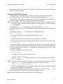
PCD-8
PCI CD/CDa 8-bit DMA Interface
for PCI Local Bus Computers
May 15, 2007
008-01182-04
PCD-8 8-bit DMA Interface User’s Guide
Copyright, Trademarks, Disclaimer
The information in this document is subject to change without notice and does not represent a commitment on the part
of Engineering Design Team, Inc. The software described in this document is furnished under a license agreement or
nondisclosure agreement. The software may be used or copied only in accordance with the terms of the agreement.
Engineering Design Team, Inc. (“EDT”), makes no warranties, express or implied, including without limitation the implied
warranties of merchantibility and fitness for a particular purpose, regarding the software described in this document (“the
software”). EDT does not warrant, guarantee, or make any representations regarding the use or the results of the use
of the software in terms of its correctness, accuracy, reliability, currentness, or otherwise. The entire risk as to the
results and performance of the software is assumed by you. The exclusion of implied warranties is not permitted by
some jurisdictions. The above exclusion may not apply to you.
In no event will EDT, its directors, officers, employees, or agents be liable to you for any consequential, incidental, or
indirect damages (including damages for loss of business profits, business interruption, loss of business information,
and the like) arising out of the use or inability to use the software even if EDT has been advised of the possibility of such
damages. Because some jurisdictions do not allow the exclusion or limitation of liability for consequential or incidental
damages, the above limitations may not apply to you. EDT’s liability to you for actual damages for any cause
whatsoever, and regardless of the form of the action (whether in contract, tort [including negligence], product liability or
otherwise), will be limited to $50 (fifty U.S. dollars).
No part of this manual may be reproduced or transmitted in any form or by any means, electronic or mechanical, without
the express written agreement of Engineering Design Team, Inc.
Copyright © Engineering Design Team, Inc. 1997–2007. All rights reserved.
EDT and Engineering Design Team are trademarks of Engineering Design Team, Inc.
Xilinx is a registered trademark of Xilinx, Inc.
EDT, Inc. May 2007
ii
Contents
PCD8 8-bit DMA Interface ............................................................................................................................ 1
Related Documents ............................................................................................................................. 1
About the DMA Interface .............................................................................................................................. 1
About the Software and Firmware ................................................................................................................ 2
The PCD Device Driver........................................................................................................................ 3
FPGA Configuration Files .................................................................................................................... 3
Software Initialization Files .................................................................................................................. 4
Sample Applications and Utilities......................................................................................................... 4
Sample Applications ....................................................................................................................................4
Utility Files ..................................................................................................................................................5
Testing Files.................................................................................................................................................5
Building Applications............................................................................................................................ 5
Configuring the PCD8................................................................................................................................... 5
Checking the PCI FPGA Firmware ...................................................................................................... 6
Loading the UI FPGA Firmware and Configuring the PCD8................................................................ 7
Using Custom FPGA Configuration Files............................................................................................. 7
Connector Pinouts ........................................................................................................................................ 8
Register Modifications ................................................................................................................................ 10
Command Register ............................................................................................................................ 10
Interface Configuration Register ........................................................................................................ 11
EDT, Inc. May 2007
iii
PCD8 8-bit DMA Interface
The PCD8 8-bit DMA Interface implements a high-speed DMA channel between an external device
and the PCI Bus host computer for the PCI SS/GS or PCI CD/CDa main boards. This document
describes modifications made to the main board firmware to implement this eight-bit bidirectional
parallel interface.
To use this interface, the PCI SS/GS main board requires an RS-422, LVDS, or ECL mezzanine board;
the PCI CD/CDa comes in either LVDS or RS-422 versions and requires no mezzanine board. Both
main boards require you to load the PCI Xilinx with the single-channel FPGA configuration file
appropriate for the board, and the user interface Xilinx with the appropriate PCD8 FPGA configuration
file.
The eight-bit Interface comprises eight input signals and eight output signals, which can transfer one
byte per clock cycle in each direction independently. The interface signals are the same as the
PCI CD/CDa signals, except that the high-order eight signals are changed to output signals and the
low-order eight are input signals.
You can use the PCD8 with the normal PCI CD/CDa cable.
Related Documents
The following related publications may prove useful:
Document
URL
EDT DMA & Digital Video Software Library www.edt.com/api (HTML)
EDT DMA & Digital Video Software Library www.edt.com/manuals/misc/api.pdf (PDF)
PCI SS/GS Main Board User’s Guide
www.edt.com/manuals/PCD/pciss_gs.pdf
PCI CD/CDa User’s Guide
www.edt.com/manuals/PCD/pcicd.pdf
About the DMA Interface
The PCD8 implements the DMA interface using two field-programmable gate arrays (FPGAs), referred
to as the PCI FPGA and the UI (user interface) FPGA:
EDT, Inc. May 2007
1
PCD8 8-bit DMA Interface User’s Guide
About the Software and Firmware
•
The PCI FPGA communicates with the host computer over the PCI Bus. It implements the DMA
engine, which transfers data between the board and the host computer, and loads its firmware on
powerup from flash ROM located on the main board.
•
The UI FPGA transfers data between the user device and the PCI FPGA; in some instances, it
also sends the data to the mezzanine board. The UI FPGA or mezzanine board may also process
the data in some manner, depending on the application.
When data comes in from the user device, the UI FPGA sends it to input and output FIFO buffers,
which smooth data transfer between the user device and the PCI Bus, as well as accommodating data
during the transition from one DMA to the next. Host DMA transfers are queued in hardware,
minimizing the amount of FIFO required.
To ensure maximum throughput, EDT’s DMA library, the DMA driver, and the FPGA configuration files
all support pipelining.
•
The library routines as well as the driver preallocate kernel resources for DMA (for example, memory), rather than waiting for an application to request a DMA transfer (typically with an EDT library
routine call such as edt_read, edt_write, or edt_start_buffers). When one DMA transfer
ends, the resources remain allocated and available for use by the next DMA transfer.
•
A portion of host memory can be configured as ring buffers: a set of buffers preallocated for DMA
and reused in round-robin fashion.
•
The FPGA fabric provides two sets of DMA registers, so that when one DMA transfer starts, the
registers required for the next are already prepared, thus enabling zero-latency transitions between DMA transfers.
You can set the number of ring buffers and their size with the EDT DMA library call
edt_configure_ring_buffers. Configure the ring buffers according to your application’s DMA
requirements — a useful configuration is often four one-megabyte ring buffers. Four ring buffers allow
one to be used for the current DMA transfer, one for pending DMA, and one for the application, with
one extra to ensure zero-latency transitions.
You can fine-tune your application to the latency requirements of a particular system by increasing or
decreasing the size of the ring buffers; slow systems may need larger ring buffers, while fast systems
may achieve better performance with more smaller ones.
Some host systems may restrict your ability to allocate particularly large ring buffers, or particularly
large numbers of them. For example, some Windows systems limit DMA resources to a maximum of
64 MB in all. If you suspect this might be a problem in your system, be sure that your code checks for
error returns after calling edt_configure_ring_buffers and before calling edt_start_buffers.
About the Software and Firmware
Install the PCD8 hardware and software according to the instructions on the software CD sleeve, using
one of the firmware files listed below:
pcda8.bit
UI Xilinx configuration file for 8-bit parallel dual-channel input/output for the PCI CDa or the
PCI SS/GS.
pcd8_src.bit
UI Xilinx configuration file for 8-bit parallel dual-channel input/output for the
PCI CD.
xtest.bit
UI Xilinx configuration file for running the test described in the section entitled
Testing in the PCI CD/CDa User’s Guide.
EDT, Inc. May 2007
2
About the Software and Firmware
PCD8 8-bit DMA Interface User’s Guide
Compatible single-channel Xilinx configuration files must be loaded in the PCI Xilinx on the main
boards. These are:
cda1.bit
PCI Xilinx configuration file for the PCI CDa.
pcd20.bit
PCI Xilinx configuration file for PCI CD-20 boards.
pcd60.bit
PCI Xilinx configuration file for PCI CD-60 boards.
pciss1.bit
Single-channel PCI Xilinx configuration file for PCI SS boards.
pcigs1.bit
Single-channel PCI Xilinx configuration file for PCI GS boards.
The following software initialization files are available for use with the initpcd automatic configuration
utility:
pcda8.cfg
Software initialization file for the PCI SS/GS and the PCI CDa.
pcd8_src.cfg
Software initialization file for the PCI CD.
The firmware file names you see in the EDT distribution do not match the file names given above
because PCI Bus slots come in two varieties: those supplying 3 V power, and those supplying 5 V
power. Different firmware is required for the two kinds of slots, but the correct firmware file is chosen
automatically when you run pciload or any other EDT-supplied firmware loading utility.
For example, you may see files named cda16_3v.bit and cda16_5v.bit, but the correct argument
to supply to load the firmware is cda16.bit.
In some cases, you may also see additional firmware files incorporating changes required for various
board revisions, or files with the same name in different subdirectories. You need not be concerned
with any of these variations of name or path, however. In all cases, the names given above are the
correct arguments to supply to the firmware-loading utilities.
The PCD Device Driver
The PCD device driver is the software running on the host that allows the host operating system to
communicate with the PCD8. The driver is loaded into the kernel upon installation, and thereafter runs
as a kernel module. The driver name and subdirectory is specific to each supported operating system;
the installation script handles those details for you, automatically installing the correct device driver in
the correct operating system-specific manner.
FPGA Configuration Files
FPGA configuration files define the firmware required for the PCI FPGA and the UI FPGA. The PCI
FPGA firmware files are in the flash subdirectory of the EDT top-level distribution directory. UI FPGA
firmware files are in the bitfiles subdirectory of the EDT top-level distribution directory.
Each FPGA must be loaded with the firmware specific to the chosen interface, and the firmware in one
FPGA must be compatible with the firmware in the other. By default, the correct FPGA configuration
file for the PCI FPGA is loaded at the factory. However, you’ll need to load the required FPGA
configuration file for the UI FPGA yourself.
The firmware files specific to your PCD8 are listed at the beginning of this section. Instructions for
loading them are provided in Configuring the PCD8.
3
EDT, Inc. May 2007
PCD8 8-bit DMA Interface User’s Guide
About the Software and Firmware
Software Initialization Files
Software initialization files (having the extension .cfg) are editable text files that run like scripts to
configure EDT boards so that they are ready to perform DMA. The commands in a software
initialization file are defined in a C application named initpcd. When you invoke initpcd, you specify
which software initialization file to use with the -f flag.
A typical software initialization file loads an FPGA configuration file into the UI FPGA and sets up
various registers to prepare the board for DMA transfers. Some software initialization files may also
load an FPGA configuration file into an FPGA residing on the mezzanine board.
A variety of software initialization files are included with the EDT software, at least one of which is
customized for each main board or main board / mezzanine board combination — that is, each FPGA
configuration file has a matching software initialization file. Software initialization files are located in
the pcd_config subdirectory of the EDT top-level distribution directory. The software initialization files
specific to your PCD8 are listed at the beginning of this section. Instructions for their use are provided
in Configuring the PCD8.
Commands defined in initpcd and typically found in software initialization files allow for specific
FPGA configuration files to be loaded (for example, bitfile:), write specified hexadecimal values to
specified registers (for example, command_reg:), enable or disable byte-swapping or short-swapping
to accommodate different operating systems’ requirements for bit ordering (for example, byteswap:),
or invoke arbitrary commands (for example, run_command:). For example:
bitfile: ssd16io.bit
command_reg: 0x08
byteswap: 1
run_command: set_ss_vco -F 1000000 2
For complete usage details, enter initpcd --help.
C source for initpcd is included so that you can add your own commands, if you wish. You can then
edit your own software initialization file to use your new commands and specify that initpcd use your
new file when configuring your board. If you would like us to include your new software initialization
commands in subsequent releases of initpcd, send mail to [email protected].
Sample Applications and Utilities
Along with the driver, the FPGA configuration files, and the software initialization files, the software CD
includes a number of applications and utilities that you can use to initialize and configure the board,
access registers, or test the board. For many of these applications and utiilities, C source is also
provided, so that you can use them as starting points to write your own applications. The most
commonly useful are described below; see the README file for the complete list.
NOTE
Software is updated regularly; the latest versions are available on our website at
www.edt.com/software.html. We encourage you to use the latest versions for new installations.
For existing applications, upgrade only if you have a specific reason to do so.
Sample Applications
rd16
Performs simple multichannel ring buffer input.
wr16
Performs simple multichannel ring buffer output.
simple_read
Performs DMA input without using ring buffers. Data is therefore subject to
interruptions, depending on system performance.
EDT, Inc. May 2007
4
Configuring the PCD8
simple_write
PCD8 8-bit DMA Interface User’s Guide
Performs DMA output without using ring buffers. Data is therefore subject to
interruptions, depending on system performance.
simple_getdata Serves as an example of a variety of DMA-related operations, including reading the
data from the connector interface and writing it to a file, as well as measuring input
rate.
simple_putdata Serves as an example of a variety of DMA-related operations, including reading
data from a file and writing it out to the connector interface.
test_timeout
Under normal operation, timeouts cancel DMA transfers. This application
exemplifies giving notification when a timeout occurs, without canceling DMA
set_ss_vco
A utility for programming the output clock or clocks on the PCD8 to specific
frequencies used by the UI FPGA for input and output.
Utility Files
initpcd
A utility for initializing and configuring the PCD8.
pdb
Utility application that enables interactive reading and writing of the PCI SS/GS UI
FPGA registers.
Testing Files
A variety of files — C source, executables, and FPGA configuration files — are available to test the
boards. Their uses are described in the documents listed under the heading Testing Procedures. They
include at least:
sslooptest
Tests most PCI SS- and PCI GS-based boards. Determines the board model and
selects the loopback test to run, then runs it.
xtest
Tests the PCI CD and CDa boards, and the single-channel DMA interface for the
PCI SS and PCI GS main boards.
Building Applications
Executable and PCD source files are at the top level of the EDT PCD driver distribution directory. If
you need to rebuild an application, therefore, run make in this directory.
Windows and Solaris users must install a C compiler. For Windows, we recommend the Microsoft
Visual C compiler; for Solaris, the Sun WorkShop C compiler. Linux users can use the gcc compiler
typically included with your Linux installation. If Solaris or Windows users wish to use gcc, contact
[email protected].
After you’ve built an application, use the --help command line option for a list of usage options and
descriptions.
Configuring the PCD8
For the PCD8 to operate as you require, it must be loaded with the appropriate FPGA configuration
files for both FPGAs. The PCI FPGA is loaded from flash ROM, which is shipped from the factory
already loaded with the appropriate FPGA configuration file; however, you must load the UI FPGA
yourself.
5
EDT, Inc. May 2007
PCD8 8-bit DMA Interface User’s Guide
Configuring the PCD8
Before loading the UI FPGA, however, you may wish to check the firmware in the PCI FPGA to ensure
that it is correct and up-to-date.
Checking the PCI FPGA Firmware
When upgrading to a new device driver, or switching to a FPGA configuration file with special
functionality, you may also need to reprogram the PCI interface flash PROM using pciload.
The following procedure applies to standard firmware only. If you are running a custom firmware file
and need to update it, first get a custom firmware configuation file from EDT.
NOTE
The presence of a newer version of the firmware with a new driver doesn’t necessarily mean that
the firmware must be updated; if a package contains a mandatory upgrade, it is prominently stated
in the README file.
On UNIX systems, pciload is an application in the installation directory /opt/EDTpcd.
On Windows systems, double-click the Pcd Utilities icon to bring up a command shell in the installation
directory \EDT\Pcd.
On Macintosh systems, pciload is an application in the installation directory
/Applications/EDT/pcd.
To see currently installed and recognized EDT boards and drivers, enter:
pciload
The program outputs the date and revision number of the firmware in the PROM.
To compare the PCI FPGA firmware in the package with the one already loaded on the board, enter:
pciload verify
The program compares the firmware in the PROM against the firmware file in the installation directory.
If they match, there’s no need to upgrade the firmware. If they differ, you’ll see error messages. This
does not necessarily indicate a problem; if your application is operating correctly, you may not need
to upgrade the firmware.
If you wish to update the standard firmware, enter:
pciload update
1. To upgrade or switch to a custom firmware file, enter:
pciload firmware_filename
replacing firmware_filename with the name of the PCI FPGA configuration file, with or without
the .bit file extension.
NOTE
If the host computer holds more than one board, you can specify the correct board to load with the
optional unit_number argument (by default, 0 for the first or only board in a host):
pciload -u unit_number filename
2. At the prompt, press Enter to confirm the loading operation. (If the file date is older than the PROM
ID date, you may need to press Enter twice.)
The board reloads the firmware from the PROM only during power-up, so after running pciload, the
old firmware remains in the PCI FPGA until the system has power-cycled.
NOTE
Updating the firmware requires cycling power, not simply rebooting.
EDT, Inc. May 2007
6
Configuring the PCD8
PCD8 8-bit DMA Interface User’s Guide
For a list of all pciload options, enter:
pciload --help
Loading the UI FPGA Firmware and Configuring the PCD8
The utility initpcd loads the UI FPGA configuration files, programs the registers, sets the clocks (if
necessary), and gets the PCD8 mezzanine board ready to perform DMA. This utility takes, as an
argument, a software initialization file, and then automatically runs the pertinent commands.
If you use initpcd to configure the PCD8, your application can concern itself solely with performing
DMA and other application-specific operations; it will therefore omit PCD8-specific operations and be
portable to other EDT boards that peform DMA.
To configure the PCD8, enter:
initpcd -u unit_number -f pcd_config/filename.cfg
replacing unit_number with the number of the board (by default, 0), and replacing filename with
one of the initialization files listed in About the Software and Firmware; for example:
initpcd -f pcda8.cfg
NOTE
Software initialization files are editable text files. If the files provided don’t meet your needs, copy
and modify the one that’s closest to your required configuration, then run initpcd with your new
file.
Using Custom FPGA Configuration Files
You can substitute your own FPGA configuration file, if necessary. If you wish to develop your own
VHDL design, contact EDT. When you’re done, be sure to create a new software initialization file for
your new firmware file and update the pcd_config directory to include it.
7
EDT, Inc. May 2007
PCD8 8-bit DMA Interface User’s Guide
Connector Pinouts
Connector Pinouts
Table 1 describes the connection from the PCI CD/CDa board to the cable.
Table 1. PCI CD (pcd8_src.bit), PCI CDa (pcda8.bit) Connector Pinout
Pin
Signal
Pin
Signal
1
ground
41
ground
2
ground (spare on CDa)
42
ground (spare on CDa)
3
DATI4+
43
DATI0+
4
DATI4–
44
DATI0–
5
DATI5+
45
DATI1+
6
DATI5–
46
DATI1–
7
DATI6+
47
DATI2+
8
DATI6–
48
DATI2–
9
DATI7+
49
DATI3+
10
DATI7–
50
DATI3–
11
DATO4+
51
DATO0+
12
DATO4–
52
DATO0–
13
DATO5+
53
DATO1+
14
DATO5–
54
DATO1–
15
DATO6+
55
DATO2+
16
DATO6–
56
DATO2–
17
DATO7+
57
DATO3+
18
DATO7–
58
DATO3–
19
spare 0+
59
spare 0–
20
+5V
60
+5V
21
spare 1+
61
spare 1–
22
spare 2+
62
spare 2–
23
ground
63
ground
24
STAT0+
64
RXT+
25
STAT0–
65
RXT–
26
STAT1+
66
IDV+
27
STAT1–
67
IDV–
28
STAT2+
68
DNR+
29
STAT2–
69
DNR–
30
STAT3+
70
reserved+
31
STAT3–
71
reserved–
32
FUNCT0+
72
SENDT+
33
FUNCT0–
73
SENDT–
34
FUNCT1+
74
ODV+
35
FUNCT1–
75
ODV–
36
FUNCT2+
76
BNR+
37
FUNCT2–
77
BNR–
38
FUNCT3+
78
TXT+
39
FUNCT3–
79
TXT–
40
ground
80
ground
EDT, Inc. May 2007
8
Connector Pinouts
PCD8 8-bit DMA Interface User’s Guide
Table 2 describes the connection from the PCI SS/GS board to the cable.
Table 2. PCI SS/GS (pcda8.bit) Connector Pinout
9
Pin
Signal
Pin
1
TXT+
35
Signal
TXT–
2
DATI0+
36
DATI0–
3
DATI1+
37
DATI1–
4
DATI2+
38
DATI2–
5
DATI3+
39
DATI3–
6
DATI4+
40
DATI4–
7
DATI5+
41
DATI5–
8
DATI6+
42
DATI6–
9
DATI7+
43
DATI7–
10
DATO0–
44
DATO0–
11
DATO1+
45
DATO1–
12
STAT3+
46
STAT3–
13
DATO2+
47
DATO2–
14
DATO3+
48
DATO3–
15
DATO4+
49
DATO4–
16
DATO5+
50
DATO5–
17
FUNCT1+
51
FUNCT1–
18
FUNCT2+
52
FUNCT2–
19
DATO6+
53
DATO6–
20
DATO7+
54
DATO7–
21
spare 0+
55
spare 0–
22
STAT0+
56
STAT0–
23
FUNCT0+
57
FUNCT0–
24
reserved
58
reserved
25
DNR+
59
DNR–
26
IDV+
60
IDV–
27
STAT1+
61
STAT1–
28
STAT2+
62
STAT2–
29
RXT+
63
RXT–
30
FUNCT3+
64
FUNCT3–
31
SENDT+
65
SENDT–
32
ODV+
66
ODV–
33
BNR+
67
BNR–
34
ground
68
ground
EDT, Inc. May 2007
PCD8 8-bit DMA Interface User’s Guide
Register Modifications
Register Modifications
The registers are as described in the PCI CD/CDa User’s Guide except for the changes described
below.
Command Register
In this register, bit 2 is different from its implementation in the PCI CD/CDa firmware.
Size
8-bit
I/O
read-write
Address
0x00
Access
PCD_CMD
Bit
PCD_
Description
4–7
STAT_INT_EN
A value of one enables the corresponding STAT bit to cause an interrupt when
it is asserted.
3
ENABLE
Set to one to enable the PCD8 interface. This bit is set after the direction is
chosen and typically after the first DMA buffer is ready. To reset direction or
flags, toggle this bit.
To flush the DMA FIFOs, clear then set this bit.
2
INV
When set, inverts the bits in each byte, so that ones become zeroes and zeroes
become ones.
1
FORCEBNR
A value of 1indicates that the board is not ready.
0
DIR
A value of 1 indicates that data is coming in to the PCD8.
A value of 0 indicates that data is going out from the PCD8.
EDT, Inc. May 2007
10
Register Modifications
PCD8 8-bit DMA Interface User’s Guide
Interface Configuration Register
In this register, bit 2 is different from its implementation in the PCI CD/CDa firmware.
Size
8-bit
I/O
read-write
Address
0x0F
Access
PCD_CONFIG
Bit
PCD_
Description
7
SETIDV
Set input data valid (used for debugging).
6
PIOEN
Enables programmed I/O. A value of 1 translates DMA channel
buffers and enables the Programmed I/O Low Register and the
Programmed I/O High Register. Write the desired 16-bit word, the
low eight bits first to the Programmed I/O Low Register, and then the
high eight bits to the Programmed I/O High Register. When the
Programmed I/O High Register is written to, the firmware generates
an ODV pulse in mid-clock, to enable the device to latch the data.
5
SETDNR
Set this bit to stop transfer to the device, as if the device had set DNR.
4
DED
Disable output delay. If set, may cause ODV transitioning on DMA
start and underflows.
3
SHORTSWAP
Set to 1 if the host computer writes the first 16-bit word on bits 16–31
of the PCI data bus (bigendian format) instead of bits 0–15 as defined
in the PCI Bus specification.
2
BITREV
Reverses the order of the bits within each byte
1
SELRXT
PCI CDa only: Set to select RXT as the source for TXT and SENDT.
(See the PCI CD/CDa User’s Guide for descriptions of these
signals.)
0
BYTESWAP
A value of 1 swaps the order of bytes in a 16-bit word of data coming
in from the data source.
PCI CD: not used.
Figure 1 shows the structure of a 32-bit data word.
Figure 1. Data Word Structure Without Swapping
short 1
short 0
31 30 29 28 27 26 25 24 23 22 21 20 19 18 17 16 15 14 13 12 11 10 9
byte 3
11
byte 2
byte 1
8
7
6
5
4
3
2
1
0
byte 0
EDT, Inc. May 2007