1
Register Modifications
PCD8 8-bit DMA Interface User’s Guide
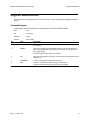
Interface Configuration Register
In this register, bit 2 is different from its implementation in the PCI CD/CDa firmware.
Size
8-bit
I/O
read-write
Address
0x0F
Access
PCD_CONFIG
Bit
PCD_
Description
7
SETIDV
Set input data valid (used for debugging).
6
PIOEN
Enables programmed I/O. A value of 1 translates DMA channel
buffers and enables the Programmed I/O Low Register and the
Programmed I/O High Register. Write the desired 16-bit word, the
low eight bits first to the Programmed I/O Low Register, and then the
high eight bits to the Programmed I/O High Register. When the
Programmed I/O High Register is written to, the firmware generates
an ODV pulse in mid-clock, to enable the device to latch the data.
5
SETDNR
Set this bit to stop transfer to the device, as if the device had set DNR.
4
DED
Disable output delay. If set, may cause ODV transitioning on DMA
start and underflows.
3
SHORTSWAP
Set to 1 if the host computer writes the first 16-bit word on bits 16–31
of the PCI data bus (bigendian format) instead of bits 0–15 as defined
in the PCI Bus specification.
2
BITREV
Reverses the order of the bits within each byte
1
SELRXT
PCI CDa only: Set to select RXT as the source for TXT and SENDT.
(See the PCI CD/CDa User’s Guide for descriptions of these
signals.)
0
BYTESWAP
A value of 1 swaps the order of bytes in a 16-bit word of data coming
in from the data source.
PCI CD: not used.
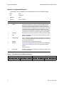
Figure 1 shows the structure of a 32-bit data word.
Figure 1. Data Word Structure Without Swapping
short 1
short 0
31 30 29 28 27 26 25 24 23 22 21 20 19 18 17 16 15 14 13 12 11 10 9
byte 3
11
byte 2
byte 1
8
7
6
5
4
3
2
1
0
byte 0
EDT, Inc. May 2007