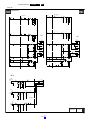
1
Color Television Chassis L11M1.1L LA 19080_000_110301.eps 110329 Contents Page 1. 2. 3. 4. 5. 6. 7. 8. 9. Revision List 2 Technical Specifications and Connections 2 Precautions, Notes, and Abbreviation List 6 Mechanical Instructions 10 Service Modes, Error Codes, and Fault Finding 19 Alignments 25 Circuit Descriptions 28 IC Data Sheets 36 Block Diagrams Wiring Diagram 32" (Thriller) 45 Wiring Diagram 40" (Thriller) 46 Wiring Diagram 32" (Berlinale) 47 Wiring Diagram 40" (Berlinale) 48 Block Diagram Video 3939 123 65052 49 Block Diagram Audio 3939 123 65052 50 Block Diagram Control & Clock Signals 3939 123 65052 51 Block Diagram I2C 3939 123 65052 52 Supply Lines Overview 3939 123 65052 53 Block Diagram Video 3939 123 65231 54 Block Diagram Audio 3939 123 65231 55 Block Diagram Control & Clock Signals 3939 123 65231 56 Block Diagram I2C 3939 123 65231 57 Supply Lines Overview 3939 123 65231 58 10. Circuit Diagrams and PWB Layouts B01 313912365052 59 B02 313912365052 60 B03 313912365052 62 B04 313912365052 63 B05 313912365052 67 B06 313912365052 69 B07 313912365052 73 313912365052 SSB Layout 74 B01 313912365231 B02 313912365231 B03 313912365231 B04 313912365231 B05 313912365231 B06 313912365231 B07 313912365231 313912365231 SSB Layout E 272217190347 Leading Edge Module E 272217190276 KEYBOARD J 272217190275 IR/LED T01 313912365071 313912365071 TCON Layout 11. Styling Sheets Styling Sheet Thriller 32" Styling Sheet Thriller 40" Styling Sheet Berlinale 32" Styling Sheet Berlinale 40" 76 77 79 80 84 86 90 91 93 95 96 98 104 105 106 107 108 © Copyright 2011 Koninklijke Philips Electronics N.V. All rights reserved. No part of this publication may be reproduced, stored in a retrieval system or transmitted, in any form or by any means, electronic, mechanical, photocopying, or otherwise without the prior permission of Philips. Published by ER/JY 1166 BU TV Consumer Care Printed in the Netherlands Subject to modification EN 3122 785 19131 2011-Jun-24 EN 2 1. Revision List L11M1.1L LA 1. Revision List Manual xxxx xxx xxxx.0 • First release. Manual xxxx xxx xxxx.1 • Chapter 2: Table 2-1 updated (added Berlinale CTNs). • Chapter 4: added wiring diagrams; see section 4.1. • Chapter 6: added white tone alignment data, see section 6.3. • Chapter 7: added Berlinale architecture diagrams; see section 7.1. 2. Technical Specifications and Connections 2.1 Index of this chapter: 2.1 Technical Specifications 2.2 Directions for Use 2.3 Connections Technical Specifications For on-line product support please use the links in Table 2-1. Here is product information available, as well as getting started, user manuals, frequently asked questions and software & drivers. Notes: • Figures can deviate due to the different set executions. • Specifications are indicative (subject to change). 2.2 T01 (LVDS Display, TCON J (IR/LED) E (Keyboard/Leading Edge) B07 (Hospitality) B06 (analog I/O, VGA) B05 (HDMI, USB) B04 (Power, DDR, LVDS) B02 (Tuner & Dig. Dem.) B01 (DC-DC) Supply lines I2C Video Audio Control & Clock Schematics Wiring Diagram 10 Block Diagrams LCD Removal 9 Mechanics Assembly Removal 4 Wire Dressing 2 Connection Overview 3139 123 xxxxx SSB B03 (Class D & mute) Table 2-1 Described Model Numbers and Diversity CTN Styling 32PFL3406D/78 Thriller 11-1 65052 2-1 4-1 4.3 4.3.2 9-1 9-5 9-6 9-7 9-8 9-9 10-1 10-2 10-3 10-4 10-5 10-6 10-7 10-18 10-19 - 32PFL3606D/78 Thriller 11-1 65052 2-1 4-1 4.3 4.3.2 9-1 9-5 9-6 9-7 9-8 9-9 10-1 10-2 10-3 10-4 10-5 10-6 10-7 10-18 10-19 - 32PFL5606D/77 Berlinale 11-3 65231 2-2 4-3 4.4 4.4.8 9-3 9-10 9-11 9-12 9-13 9-14 10-9 10-10 10-11 10-12 10-13 10-14 10-15 10-17 - - 32PFL5606D/78 Berlinale 11-3 65231 2-2 4-3 4.4 4.4.8 9-3 9-10 9-11 9-12 9-13 9-14 10-9 10-10 10-11 10-12 10-13 10-14 10-15 10-17 - - 40PFL3606D/78 Thriller 11-2 65052 2-1 4-2 4.3 4.3.2 9-2 9-5 9-6 9-7 9-8 9-9 10-1 10-2 40PFL5606D/77 Berlinale 11-4 65231 2-2 4-4 4.4 4.4.8 9-4 9-10 9-11 9-12 9-13 9-14 10-9 10-10 10-11 10-12 10-13 10-14 10-15 10-17 - - 40PFL5606D/78 Berlinale 11-4 65231 2-2 4-4 4.4 4.4.8 9-4 9-10 9-11 9-12 9-13 9-14 10-9 10-10 10-11 10-12 10-13 10-14 10-15 10-17 - - Directions for Use You can download this information from the following websites: http://www.philips.com/support http://www.p4c.philips.com 2011-Jun-24 back to div. table 10-3 10-4 10-5 10-6 10-7 10-18 10-19 10-20 10-21 Technical Specifications and Connections 2.3 L11M1.1L LA 2. EN 3 Connections REAR CONNECTORS DIGITAL AUDIO OUT CVI 1 R L Pr SIDE CONNECTORS Pb AUDIO IN DVI/VGA SERV.U Y 1 4 5 6 7 BOTTOM REAR CONNECTORS 8 2 9 10 11 3 R L Pr Pb Y HDMI 1 (ARC) CVI 2 VGA ANTENNA 19130_001_110421.eps 110421 Figure 2-1 Connection overview Thriller (xxPFL3x06/xx) REAR CONNECTORS 6 4 SIDE CONNECTORS 5 1 7 BOTTOM REAR CONNECTORS 8 12 9 10 11 2 3 19131_021_110623.eps 110623 Figure 2-2 Connection overview Berlinale (xxPFL5x06/xx) back to div. table 2011-Jun-24 EN 4 2. L11M1.1L LA Technical Specifications and Connections 2.3.3 Note: The following connector color abbreviations are used (according to DIN/IEC 757): Bk= Black, Bu= Blue, Gn= Green, Gy= Grey, Rd= Red, Wh= White, Ye= Yellow. 2.3.1 8 - CVI-2: Cinch: Video YPbPr - In, Audio - In Wh - Audio - L 0.5 VRMS / 10 k Rd - Audio - R 0.5 VRMS / 10 k Rd - Video Pr 0.7 VPP / 75 Bu - Video Pb 0.7 VPP / 75 Gn - Video Y 1 VPP / 75 Side Connections 1 - USB2.0 1 2 3 Bottom Connections 4 9 - HDMI1 Audio Return Channel: Digital Video, Digital Audio - In 10000_022_090121.eps 090121 Figure 2-3 USB (type A) 1 2 3 4 - +5V - Data (-) - Data (+) - Ground 19 18 2 - AV IN: Cinch: Video CVBS - In, Audio - In Ye - Video CVBS 1 VPP / 75 ohm Wh - Audio L 0.5 VRMS / 10 kohm Rd - Audio R 0.5 VRMS / 10 kohm Figure 2-5 HDMI (type A) connector 1 2 3 4 5 6 7 8 9 10 11 12 13 14 15 16 17 18 19 20 jq jq jq 3 - HDMI: Digital Video, Digital Audio - In 1 2 10000_017_090121.eps 090428 Figure 2-4 HDMI (type A) connector 1 2 3 4 5 6 7 8 9 10 11 12 13 14 15 16 17 18 19 20 2.3.2 - D2+ - Shield - D2- D1+ - Shield - D1- D0+ - Shield - D0- CLK+ - Shield - CLK- Easylink - n.c. - DDC_SCL - DDC_SDA - Ground - +5V - HPD - Ground Data channel Gnd Data channel Data channel Gnd Data channel Data channel Gnd Data channel Data channel Gnd Data channel Control channel/CEC j H j j H j j H j j H j jk - D2+ - Shield - D2- D1+ - Shield - D1- D0+ - Shield - D0- CLK+ - Shield - CLK- Easylink - ARC - DDC_SCL - DDC_SDA - Ground - +5V - HPD - Ground Data channel Gnd Data channel Data channel Gnd Data channel Data channel Gnd Data channel Data channel Gnd Data channel Control channel/CEC Audio Return Channel DDC clock DDC data Gnd Hot Plug Detect Gnd 10 - Aerial - In - - F-type Coax, 75 1 Hot Plug Detect Gnd 4 - CVI-1: Cinch: Video YPbPr - In, Audio - In Wh - Audio - L 0.5 VRMS / 10 k Rd - Audio - R 0.5 VRMS / 10 k Rd - Video Pr 0.7 VPP / 75 Bu - Video Pb 0.7 VPP / 75 Gn - Video Y 1 VPP / 75 5 - Cinch: Digital Audio - Out Bk - Coaxial 0.4 - 0.6VPP / 75 ohm 6 - Service Connector (UART) 1 - Ground Gnd 2 - UART_TX Transmit 3 - UART_RX Receive 7 - Mini Jack: Audio - In DVI/VGA Bk - Audio 0.5 VRMS / 10 k D 5 10 6 15 11 DDC clock DDC data Gnd j H j j H j j H j j H j jk j j jk H j j H 11 - VGA: Video RGB - In j jk H j j H 10000_002_090121.eps 090127 Figure 2-6 VGA Connector 1 2 3 4 5 6 7 8 9 10 11 12 13 14 15 Rear Connections 2011-Jun-24 1 2 10000_017_090121.eps 090428 k jk jk H Gnd 19 18 jq jq jq jq jq jq jq jq jq jq kq H k j - Video Red - Video Green - Video Blue - n.c. - Ground - Ground Red - Ground Green - Ground Blue - +5VDC - Ground Sync - n.c. - DDC_SDA - H-sync - V-sync - DDC_SCL 0.7 VPP / 75 0.7 VPP / 75 0.7 VPP / 75 j j j Gnd Gnd Gnd Gnd +5 V Gnd H H H H j H DDC data 0-5V 0-5V DDC clock j j j j 12 - HDMI2: Digital Video, Digital Audio - In (optional) 19 18 1 2 10000_017_090121.eps 090428 jo Figure 2-7 HDMI (type A) connector back to div. table Technical Specifications and Connections 1 2 3 4 5 6 7 8 9 10 11 12 13 14 15 16 17 18 19 20 - D2+ - Shield - D2- D1+ - Shield - D1- D0+ - Shield - D0- CLK+ - Shield - CLK- Easylink - n.c. - DDC_SCL - DDC_SDA - Ground - +5V - HPD - Ground Data channel Gnd Data channel Data channel Gnd Data channel Data channel Gnd Data channel Data channel Gnd Data channel Control channel/CEC j H j j H j j H j j H j jk DDC clock DDC data Gnd j jk H j j H Hot Plug Detect Gnd back to div. table L11M1.1L LA 2. EN 5 2011-Jun-24 EN 6 3. L11M1.1L LA Precautions, Notes, and Abbreviation List 3. Precautions, Notes, and Abbreviation List • Index of this chapter: 3.1 Safety Instructions 3.2 Warnings 3.3 Notes 3.4 Abbreviation List 3.1 3.3.2 Safety Instructions • • • Safety regulations require that after a repair, the set must be returned in its original condition. Pay in particular attention to the following points: • Route the wire trees correctly and fix them with the mounted cable clamps. • Check the insulation of the Mains/AC Power lead for external damage. • Check the strain relief of the Mains/AC Power cord for proper function. • Check the electrical DC resistance between the Mains/AC Power plug and the secondary side (only for sets that have a Mains/AC Power isolated power supply): 1. Unplug the Mains/AC Power cord and connect a wire between the two pins of the Mains/AC Power plug. 2. Set the Mains/AC Power switch to the “on” position (keep the Mains/AC Power cord unplugged!). 3. Measure the resistance value between the pins of the Mains/AC Power plug and the metal shielding of the tuner or the aerial connection on the set. The reading should be between 4.5 M and 12 M. 4. Switch “off” the set, and remove the wire between the two pins of the Mains/AC Power plug. • Check the cabinet for defects, to prevent touching of any inner parts by the customer. • • 3.3.3 All resistor values are in ohms, and the value multiplier is often used to indicate the decimal point location (e.g. 2K2 indicates 2.2 k). Resistor values with no multiplier may be indicated with either an “E” or an “R” (e.g. 220E or 220R indicates 220 ). All capacitor values are given in micro-farads ( 10-6), nano-farads (n 10-9), or pico-farads (p 10-12). Capacitor values may also use the value multiplier as the decimal point indication (e.g. 2p2 indicates 2.2 pF). An “asterisk” (*) indicates component usage varies. Refer to the diversity tables for the correct values. The correct component values are listed on the Philips Spare Parts Web Portal. Spare Parts For the latest spare part overview, consult your Philips Spare Part web portal. 3.3.4 BGA (Ball Grid Array) ICs Introduction For more information on how to handle BGA devices, visit this URL: http://www.atyourservice-magazine.com. Select “Magazine”, then go to “Repair downloads”. Here you will find Information on how to deal with BGA-ICs. BGA Temperature Profiles For BGA-ICs, you must use the correct temperature-profile. Where applicable and available, this profile is added to the IC Data Sheet information section in this manual. 3.3.5 3.2 Schematic Notes • Safety regulations require the following during a repair: • Connect the set to the Mains/AC Power via an isolation transformer (> 800 VA). • Replace safety components, indicated by the symbol h, only by components identical to the original ones. Any other component substitution (other than original type) may increase risk of fire or electrical shock hazard. Where necessary, measure the waveforms and voltages with (D) and without (E) aerial signal. Measure the voltages in the power supply section both in normal operation (G) and in stand-by (F). These values are indicated by means of the appropriate symbols. Lead-free Soldering Warnings • • • • 3.3 Notes 3.3.1 General • 2011-Jun-24 Due to lead-free technology some rules have to be respected by the workshop during a repair: • Use only lead-free soldering tin. If lead-free solder paste is required, please contact the manufacturer of your soldering equipment. In general, use of solder paste within workshops should be avoided because paste is not easy to store and to handle. • Use only adequate solder tools applicable for lead-free soldering tin. The solder tool must be able: – To reach a solder-tip temperature of at least 400°C. – To stabilize the adjusted temperature at the solder-tip. – To exchange solder-tips for different applications. • Adjust your solder tool so that a temperature of around 360°C - 380°C is reached and stabilized at the solder joint. Heating time of the solder-joint should not exceed ~ 4 sec. Avoid temperatures above 400°C, otherwise wear-out of tips will increase drastically and flux-fluid will be destroyed. To avoid wear-out of tips, switch “off” unused equipment or reduce heat. • Mix of lead-free soldering tin/parts with leaded soldering tin/parts is possible but PHILIPS recommends strongly to avoid mixed regimes. If this cannot be avoided, carefully clear the solder-joint from old tin and re-solder with new tin. All ICs and many other semiconductors are susceptible to electrostatic discharges (ESD w). Careless handling during repair can reduce life drastically. Make sure that, during repair, you are connected with the same potential as the mass of the set by a wristband with resistance. Keep components and tools also at this same potential. Be careful during measurements in the high voltage section. Never replace modules or other components while the unit is switched “on”. When you align the set, use plastic rather than metal tools. This will prevent any short circuits and the danger of a circuit becoming unstable. Measure the voltages and waveforms with regard to the chassis (= tuner) ground (H), or hot ground (I), depending on the tested area of circuitry. The voltages and waveforms shown in the diagrams are indicative. Measure them in the Service Default Mode with a colour bar signal and stereo sound (L: 3 kHz, R: 1 kHz unless stated otherwise) and picture carrier at 475.25 MHz for PAL, or 61.25 MHz for NTSC (channel 3). 3.3.6 Alternative BOM identification It should be noted that on the European Service website, “Alternative BOM” is referred to as “Design variant”. back to div. table Precautions, Notes, and Abbreviation List 3.4 AARA ACI ADC AFC AGC AM AP AR ASF ATSC ATV Auto TV AV AVC AVIP B/G BDS BLR BTSC 10000_053_110228.eps 110228 B-TXT C CEC Figure 3-1 Serial number (example) Board Level Repair (BLR) or Component Level Repair (CLR) CL If a board is defective, consult your repair procedure to decide if the board has to be exchanged or if it should be repaired on component level. If your repair procedure says the board should be exchanged completely, do not solder on the defective board. Otherwise, it cannot be returned to the O.E.M. supplier for back charging! CLR ComPair CP CSM CTI Practical Service Precautions CVBS • • EN 7 Abbreviation List 0/6/12 Identification: The bottom line of a type plate gives a 14-digit serial number. Digits 1 and 2 refer to the production centre (e.g. SN is Lysomice, RJ is Kobierzyce), digit 3 refers to the B.O.M. code, digit 4 refers to the Service version change code, digits 5 and 6 refer to the production year, and digits 7 and 8 refer to production week (in example below it is 2010 week 10 / 2010 week 17). The 6 last digits contain the serial number. 3.3.8 3. powered TV set, it is best to test the high voltage insulation. It is easy to do, and is a good service precaution. The third digit in the serial number (example: AG2B0335000001) indicates the number of the alternative B.O.M. (Bill Of Materials) that has been used for producing the specific TV set. In general, it is possible that the same TV model on the market is produced with e.g. two different types of displays, coming from two different suppliers. This will then result in sets which have the same CTN (Commercial Type Number; e.g. 28PW9515/12) but which have a different B.O.M. number. By looking at the third digit of the serial number, one can identify which B.O.M. is used for the TV set he is working with. If the third digit of the serial number contains the number “1” (example: AG1B033500001), then the TV set has been manufactured according to B.O.M. number 1. If the third digit is a “2” (example: AG2B0335000001), then the set has been produced according to B.O.M. no. 2. This is important for ordering the correct spare parts! For the third digit, the numbers 1...9 and the characters A...Z can be used, so in total: 9 plus 26= 35 different B.O.M.s can be indicated by the third digit of the serial number. 3.3.7 L11M1.1L LA It makes sense to avoid exposure to electrical shock. While some sources are expected to have a possible dangerous impact, others of quite high potential are of limited current and are sometimes held in less regard. Always respect voltages. While some may not be dangerous in themselves, they can cause unexpected reactions that are best avoided. Before reaching into a DAC DBE DCM DDC back to div. table SCART switch control signal on A/V board. 0 = loop through (AUX to TV), 6 = play 16 : 9 format, 12 = play 4 : 3 format Automatic Aspect Ratio Adaptation: algorithm that adapts aspect ratio to remove horizontal black bars; keeps the original aspect ratio Automatic Channel Installation: algorithm that installs TV channels directly from a cable network by means of a predefined TXT page Analogue to Digital Converter Automatic Frequency Control: control signal used to tune to the correct frequency Automatic Gain Control: algorithm that controls the video input of the feature box Amplitude Modulation Asia Pacific Aspect Ratio: 4 by 3 or 16 by 9 Auto Screen Fit: algorithm that adapts aspect ratio to remove horizontal black bars without discarding video information Advanced Television Systems Committee, the digital TV standard in the USA See Auto TV A hardware and software control system that measures picture content, and adapts image parameters in a dynamic way External Audio Video Audio Video Controller Audio Video Input Processor Monochrome TV system. Sound carrier distance is 5.5 MHz Business Display Solutions (iTV) Board-Level Repair Broadcast Television Standard Committee. Multiplex FM stereo sound system, originating from the USA and used e.g. in LATAM and AP-NTSC countries Blue TeleteXT Centre channel (audio) Consumer Electronics Control bus: remote control bus on HDMI connections Constant Level: audio output to connect with an external amplifier Component Level Repair Computer aided rePair Connected Planet / Copy Protection Customer Service Mode Color Transient Improvement: manipulates steepness of chroma transients Composite Video Blanking and Synchronization Digital to Analogue Converter Dynamic Bass Enhancement: extra low frequency amplification Data Communication Module. Also referred to as System Card or Smartcard (for iTV). See “E-DDC” 2011-Jun-24 EN 8 3. D/K DFI DFU DMR DMSD DNM DNR DRAM DRM DSP DST DTCP DVB-C DVB-T DVD DVI(-d) E-DDC EDID EEPROM EMI EPG EPLD EU EXT FDS FDW FLASH FM FPGA FTV Gb/s G-TXT H HD HDD HDCP HDMI HP I I2 C I2 D I2 S IF IR IRQ ITU-656 2011-Jun-24 L11M1.1L LA Precautions, Notes, and Abbreviation List Monochrome TV system. Sound carrier distance is 6.5 MHz Dynamic Frame Insertion Directions For Use: owner's manual Digital Media Reader: card reader Digital Multi Standard Decoding Digital Natural Motion Digital Noise Reduction: noise reduction feature of the set Dynamic RAM Digital Rights Management Digital Signal Processing Dealer Service Tool: special remote control designed for service technicians Digital Transmission Content Protection; A protocol for protecting digital audio/video content that is traversing a high speed serial bus, such as IEEE-1394 Digital Video Broadcast - Cable Digital Video Broadcast - Terrestrial Digital Versatile Disc Digital Visual Interface (d= digital only) Enhanced Display Data Channel (VESA standard for communication channel and display). Using E-DDC, the video source can read the EDID information form the display. Extended Display Identification Data (VESA standard) Electrically Erasable and Programmable Read Only Memory Electro Magnetic Interference Electronic Program Guide Erasable Programmable Logic Device Europe EXTernal (source), entering the set by SCART or by cinches (jacks) Full Dual Screen (same as FDW) Full Dual Window (same as FDS) FLASH memory Field Memory or Frequency Modulation Field-Programmable Gate Array Flat TeleVision Giga bits per second Green TeleteXT H_sync to the module High Definition Hard Disk Drive High-bandwidth Digital Content Protection: A “key” encoded into the HDMI/DVI signal that prevents video data piracy. If a source is HDCP coded and connected via HDMI/DVI without the proper HDCP decoding, the picture is put into a “snow vision” mode or changed to a low resolution. For normal content distribution the source and the display device must be enabled for HDCP “software key” decoding. High Definition Multimedia Interface HeadPhone Monochrome TV system. Sound carrier distance is 6.0 MHz Inter IC bus Inter IC Data bus Inter IC Sound bus Intermediate Frequency Infra Red Interrupt Request The ITU Radio communication Sector (ITU-R) is a standards body iTV LS LATAM LCD LED L/L' LPL LS LVDS Mbps M/N MHEG MIPS MOP MOSFET MPEG MPIF MUTE MTV NC NICAM NTC NTSC NVM O/C OSD OAD OTC P50 back to div. table subcommittee of the International Telecommunication Union relating to radio communication. ITU-656 (a.k.a. SDI), is a digitized video format used for broadcast grade video. Uncompressed digital component or digital composite signals can be used. The SDI signal is self-synchronizing, uses 8 bit or 10 bit data words, and has a maximum data rate of 270 Mbit/s, with a minimum bandwidth of 135 MHz. Institutional TeleVision; TV sets for hotels, hospitals etc. Last Status; The settings last chosen by the customer and read and stored in RAM or in the NVM. They are called at start-up of the set to configure it according to the customer's preferences Latin America Liquid Crystal Display Light Emitting Diode Monochrome TV system. Sound carrier distance is 6.5 MHz. L' is Band I, L is all bands except for Band I LG.Philips LCD (supplier) Loudspeaker Low Voltage Differential Signalling Mega bits per second Monochrome TV system. Sound carrier distance is 4.5 MHz Part of a set of international standards related to the presentation of multimedia information, standardised by the Multimedia and Hypermedia Experts Group. It is commonly used as a language to describe interactive television services Microprocessor without Interlocked Pipeline-Stages; A RISC-based microprocessor Matrix Output Processor Metal Oxide Silicon Field Effect Transistor, switching device Motion Pictures Experts Group Multi Platform InterFace MUTE Line Mainstream TV: TV-mode with Consumer TV features enabled (iTV) Not Connected Near Instantaneous Compounded Audio Multiplexing. This is a digital sound system, mainly used in Europe. Negative Temperature Coefficient, non-linear resistor National Television Standard Committee. Color system mainly used in North America and Japan. Color carrier NTSC M/N= 3.579545 MHz, NTSC 4.43= 4.433619 MHz (this is a VCR norm, it is not transmitted off-air) Non-Volatile Memory: IC containing TV related data such as alignments Open Circuit On Screen Display Over the Air Download. Method of software upgrade via RF transmission. Upgrade software is broadcasted in TS with TV channels. On screen display Teletext and Control; also called Artistic (SAA5800) Project 50: communication protocol between TV and peripherals Precautions, Notes, and Abbreviation List PAL PCB PCM PDP PFC PIP PLL POD POR PSDL PSL PSLS PTC PWB PWM QRC QTNR QVCP RAM RGB RC RC5 / RC6 RESET ROM RSDS R-TXT SAM S/C SCART SCL SCL-F SD SDA SDA-F SDI SDRAM SECAM SIF SMPS SoC SOG SOPS SPI S/PDIF SRAM SRP SSB SSC Phase Alternating Line. Color system mainly used in West Europe (colour carrier = 4.433619 MHz) and South America (colour carrier PAL M = 3.575612 MHz and PAL N = 3.582056 MHz) Printed Circuit Board (same as “PWB”) Pulse Code Modulation Plasma Display Panel Power Factor Corrector (or Preconditioner) Picture In Picture Phase Locked Loop. Used for e.g. FST tuning systems. The customer can give directly the desired frequency Point Of Deployment: a removable CAM module, implementing the CA system for a host (e.g. a TV-set) Power On Reset, signal to reset the uP Power Supply for Direct view LED backlight with 2D-dimming Power Supply with integrated LED drivers Power Supply with integrated LED drivers with added Scanning functionality Positive Temperature Coefficient, non-linear resistor Printed Wiring Board (same as “PCB”) Pulse Width Modulation Quasi Resonant Converter Quality Temporal Noise Reduction Quality Video Composition Processor Random Access Memory Red, Green, and Blue. The primary color signals for TV. By mixing levels of R, G, and B, all colors (Y/C) are reproduced. Remote Control Signal protocol from the remote control receiver RESET signal Read Only Memory Reduced Swing Differential Signalling data interface Red TeleteXT Service Alignment Mode Short Circuit Syndicat des Constructeurs d'Appareils Radiorécepteurs et Téléviseurs Serial Clock I2C CLock Signal on Fast I2C bus Standard Definition Serial Data I2C DAta Signal on Fast I2C bus Serial Digital Interface, see “ITU-656” Synchronous DRAM SEequence Couleur Avec Mémoire. Colour system mainly used in France and East Europe. Colour carriers = 4.406250 MHz and 4.250000 MHz Sound Intermediate Frequency Switched Mode Power Supply System on Chip Sync On Green Self Oscillating Power Supply Serial Peripheral Interface bus; a 4wire synchronous serial data link standard Sony Philips Digital InterFace Static RAM Service Reference Protocol Small Signal Board STB STBY SVGA SVHS SW SWAN SXGA TFT THD TMDS TS TXT TXT-DW UI uP UXGA V VESA VGA VL VSB WYSIWYR WXGA XTAL XGA Y Y/C YPbPr YUV back to div. table L11M1.1L LA 3. EN 9 Spread Spectrum Clocking, used to reduce the effects of EMI Set Top Box STand-BY 800 × 600 (4:3) Super Video Home System Software Spatial temporal Weighted Averaging Noise reduction 1280 × 1024 Thin Film Transistor Total Harmonic Distortion Transmission Minimized Differential Signalling Transport Stream TeleteXT Dual Window with TeleteXT User Interface Microprocessor 1600 × 1200 (4:3) V-sync to the module Video Electronics Standards Association 640 × 480 (4:3) Variable Level out: processed audio output toward external amplifier Vestigial Side Band; modulation method What You See Is What You Record: record selection that follows main picture and sound 1280 × 768 (15:9) Quartz crystal 1024 × 768 (4:3) Luminance signal Luminance (Y) and Chrominance (C) signal Component video. Luminance and scaled color difference signals (B-Y and R-Y) Component video 2011-Jun-24 EN 10 4. L11M1.1L LA Mechanical Instructions 4. Mechanical Instructions Index of this chapter: 4.1 Cable Dressing 4.2 Service Positions 4.3 Assy/Panel Removal (Thriller styling; xxPFL3x06D/xx) 4.4 Assy/Panel Removal (Berlinale styling; xxPFL5x06D/xx) 4.5 Set Re-assembly 4.1 Notes: • Figures below can deviate slightly from the actual situation, due to the different set executions. Cable Dressing 19130_002_110421.eps 110421 Figure 4-1 Cable dressing 32" Thriller (xxPFL3x06D/xx) 2011-Jun-24 back to div. table Mechanical Instructions L11M1.1L LA 4. EN 11 11 mm saddle × 1 150 mm tape × 3 70 mm tape × 4 Foam × 2 19130_003_110426.eps 110426 Figure 4-2 Cable dressing 40" Thriller (xxPFL3x06D/xx) back to div. table 2011-Jun-24 EN 12 4. L11M1.1L LA Mechanical Instructions 19131_025_110623.eps 110623 Figure 4-3 Cable dressing 32" Berlinale (xxPFL5x06D/xx) 2011-Jun-24 back to div. table Mechanical Instructions L11M1.1L LA 4. EN 13 19131_026_110623.eps 110623 Figure 4-4 Cable dressing 40" Berlinale (xxPFL5x06D/xx) back to div. table 2011-Jun-24 EN 14 4.2 4. Mechanical Instructions L11M1.1L LA Service Positions measurements and alignments. When using foam bars take care that these always support the cabinet and never only the display. Caution: Failure to follow these guidelines can seriously damage the display! Ensure that ESD safe measures are taken. For easy servicing of a TV set, the set should be put face down on a soft flat surface, foam buffers or other specific workshop tools. Ensure that a stable situation is created to perform 4.3 Assy/Panel Removal (Thriller styling; xxPFL3x06D/xx) Instructions below apply to the 40PFL3606D/78, but will be similar for other models. 4.3.1 Rear Cover 2 3 2 2 2 3 3 3 2 2 3 3 2 3 3 1 2 3 3 1 1 1 1 3 2 19130_004_110426.eps 110426 Figure 4-5 Rear cover removal (40") Warning: Disconnect the mains power cord before removing the rear cover. See Figure 4-5. 1. Remove fixation screws [2] and [3] that secure the rear cover. It is not necessary to remove the stand first [1]. 2. Lift the rear cover from the TV. Make sure that wires and flat foils are not damaged while lifting the rear cover from the set. 2011-Jun-24 back to div. table Mechanical Instructions 4.3.2 4. 5. 6. 7. LCD Panel Refer to Figure 4-6 for details. 1. Remove the Stand [A]. 2. Remove the Speakers/Subwoofer [B]. 3. Remove the PSU [C], SSB [D] and TCON (E). 1 L11M1.1L LA 4. EN 15 Remove the IR/LED board [F]. Remove the Local Control board [G]. Remove the clamps [1]. Remove all metal subframes [2] that do not belong to the LCD display. 1 1 2 1 1 2 1 C 1 E 2 1 B 1 2 1 D G F 1 1 A 1 19130_006_110426.eps 110426 Figure 4-6 LCD Panel removal (based on 40" model) 4.4 Assy/Panel Removal (Berlinale styling; xxPFL5x06D/xx) Instructions below apply to the 40PFL5606H/12 (European model), but will be similar for other models. 4.4.1 Rear Cover Refer to Figure 4-7 to Figure 4-9 for details. Warning: Disconnect the mains power cord before removing the rear cover. 1. Remove screw caps [1] that cover VESA screw holes. 2. Remove all fixation screws [2], [3] that secure the rear cover. 3. Release the bottom catches [4], [5]. 4. At the indicated areas [6] the cover is secured by clips. Be very careful with releasing those. 5. Lift the rear cover from the TV starting from the bottom [7] and tilt it vertically [8]. Make sure that wires and flat foils are not damaged while lifting the rear cover from the set. back to div. table 2011-Jun-24 EN 16 4. Mechanical Instructions L11M1.1L LA 2 2 2 2 1 1 6 2 2 2 3 8 8 2 2 1 2 1 2 3 2 2 2 7 7 19150_006_110512.eps 110512 Figure 4-7 Rear cover removal -14.4.2 4 Caution: it is mandatory to remount all different screws at their original position during re-assembly. Failure to do so may result in damaging the SSB. 1. Release the clips from both the LVDS Flat Foil connectors that connect with the SSB. Caution: be careful, as these are very fragile connectors! Take the flat foils out of their connectors. 2. Unplug all other connectors. 3. Remove all fixation screws from the SSB. Note that one screw is located below the upper flat foil cable. 4. Take out the SSB together with side and bottom I/O bracket. 5. Remove the screws between the bottom Y-Pb and L-R audio connectors. 6. Remove the side and bottom I/O bracket from the SSB. Note that these parts are kept in place by very fragile clips. Release those clips gently! 4 19150_013_110513.eps 110513 Figure 4-8 Rear cover removal -2- 4.4.3 Power Supply Unit (PSU) Caution: it is mandatory to remount all different screws at their original position during re-assembly. Failure to do so may result in damaging the PSU. 1. Release the tape from the Power board cables. 2. Unplug power connectors from the SSB, as it is not unplugable at the PSU itself (soldered connector). 3. Unplug both other connectors from the PSU. 4. Remove all fixation screws from the PSU. 5. The PSU can be taken out of the set now. When defective, replace the whole unit. 5 19150_014_110513.eps 110513 Figure 4-9 Rear cover removal -3- 2011-Jun-24 Small Signal Board (SSB) back to div. table Mechanical Instructions 4.4.4 L11M1.1L LA 4. EN 17 Stand removal 1. Remove the four fixation screws. 2. Take the stand out in a downwards direction. 4.4.5 Stand bracket removal Refer to Figure 4-10 for details. Caution: it is mandatory to remount all different screws at their original position during re-assembly. Be sure to put the set in the Service Position. 1. Remove the fixation screws [1], [2]. 2. Take the Stand bracket out. 2 3 1 1 2 19150_009_110512.eps 110512 2 3 2 Figure 4-12 IR/LED/Keyboard removal 4.4.8 Stand Bracket 2 3 1 1 Refer to Figure 4-14 for details. 1. Remove the SSB as described earlier. 2. Remove the PSU as described earlier. 3. Remove the stand as described earlier. 4. Remove the stand bracket as described earlier. 5. Remove the Power switch and mains plug as described earlier and remove the plastic subframe. 6. Remove the speakers. 7. Remove all tapes that secure any cable and remove the cables from the set. 8. Release the clips from the LVDS flat foil connector [1]. Caution: be careful, as these are very fragile cables and connectors! Take the flat foil out of it’s connector. 9. Release the metal clips [2] at the top, sides and bottom of the panel that secure the LCD panel with the bezel and remove the clips from their position. Be careful not to break the plastic catches [3] that secure the metal brackets. 10. Lift the LED Panel from the bezel. When defective, replace the whole unit. 2 19150_007_110512.eps 110512 Figure 4-10 Stand bracket removal 4.4.6 LCD Panel Power switch and mains plug Refer to Figure 4-11 for details. 1. Unplug the connector from the PSU. 2. The switch and mains inlet can be removed by lifting the catches with a screwdriver [1] and sliding them out [2]. When defective, replace the power switch and mains plug assembly. 1 2 2 3 3 2 19150_010_110512.eps 110512 19150_008_110512.eps 110512 Figure 4-13 LCD Panel removal -1- Figure 4-11 Power switch and mains plug removal 4.4.7 IR/LED/Keyboard Refer to Figure 4-12 for details. 1. Remove the stand bracket as described earlier. 2. Remove the screws [1] that connect the IR/LED/Keyboard to the bezel. When defective, replace the whole unit. back to div. table 2011-Jun-24 EN 18 4. L11M1.1L LA Mechanical Instructions 2 2 2 2 2 2 2 2 1 2 2 2 2 2 2 2 2 19150_011_110512.eps 110512 Figure 4-14 LCD Panel removal -2- 4.5 Set Re-assembly To re-assemble the whole set, execute all processes in reverse order. Notes: • While re-assembling, make sure that all cables are placed and connected in their original position. See Figure 4-15 • Pay special attention not to damage the EMC foams in the set. Ensure that EMC foams are mounted correctly. Panel Thinner blue FFC supporting tape belong to Panel side Proper FFC insertion: Silver line is not visible when connector lock is closed TCON Thicker blue FFC supporting tape belong to SSB side Improper FFC insertion: Silver line is visible when connector lock is closed 19130_007_110426.eps 110426 Figure 4-15 Flat Foil Cable (FFC) precautions 2011-Jun-24 back to div. table Service Modes, Error Codes, and Fault Finding L11M1.1L LA 5. EN 19 5. Service Modes, Error Codes, and Fault Finding 5.2.1 Index of this chapter: 5.1 Test Points 5.2 Service Modes 5.3 Service Tools 5.4 Error Codes 5.5 The Blinking LED Procedure 5.6 Fault Finding and Repair Tips 5.7 Repair Policy TCON Boards 5.8 Software Upgrading 5.1 Next items are applicable to all Service Modes or are general. Life Timer During the life time cycle of the TV set, a timer is kept (called “Op. Hour”). It counts the normal operation hours (not the Stand-by hours). The actual value of the timer is displayed in SDM and SAM in a decimal value. Every two soft-resets increase the hour by +1. Stand-by hours are not counted. Test Points Software Identification, Version, and Cluster The software ID, version, and cluster will be shown in the main menu display of SDM, SAM, and CSM. The screen will show: “AAAAAAB-XX.YY”, where: • AAAAAA is the chassis name: L11M11. • B is the region indication: E= Europe, A= AP/China, U= NAFTA, L= LATAM. • XX is the main version number: this is updated with a major change of specification (incompatible with the previous software version). Numbering will go from 01 - 99 and AA ZZ. – If the main version number changes, the new version number is written in the NVM. – If the main version number changes, the default settings are loaded. • YY is the sub version number: this is updated with a minor change (backwards compatible with the previous versions) Numbering will go from 00 - 99. – If the sub version number changes, the new version number is written in the NVM. – If the NVM is fresh, the software identification, version, and cluster will be written to NVM. In the chassis schematics and layout overviews, the test points are mentioned. In the schematics and layouts, test points are indicated with “Fxxx” or “Ixxx”. As most signals are digital, it will be difficult to measure waveforms with a standard oscilloscope. Several key ICs are capable of generating test patterns, which can be controlled via ComPair. In this way it is possible to determine which part is defective. Perform measurements under the following conditions: • Service Default Mode. • Video: Color bar signal. • Audio: 3 kHz left, 1 kHz right. Service Modes The Service Mode feature is split into four parts: • Service Default Mode (SDM). • Service Alignment Mode (SAM). • Customer Service Mode (CSM). • Computer Aided Repair Mode (ComPair). Display Option Code Selection When after an SSB or display exchange, the display option code is not set properly, it will result in a TV with “no display”. Therefore, it is required to set this display option code after such a repair. To do so, press the following key sequence on a standard RC transmitter: “062598” directly followed by MENU/HOME and “xxx”, where “xxx” is a 3 digit decimal value of the panel type, see sticker on the side/bottom of the cabinet. When the value is accepted and stored in NVM, the set will switch to Stand-by, to indicate that the process has been completed. SDM and SAM offer features, which can be used by the Service engineer to repair/align a TV set. Some features are: • A pre-defined situation to ensure measurements can be made under uniform conditions (SDM). • Activates the blinking LED procedure for error identification when no picture is available (SDM). • The possibility to overrule software protections when SDM is entered via the Service pins. • Make alignments (e.g. White Tone), (de)select options, enter options codes, reset the error buffer (SAM). • Display information (“SDM” or “SAM” indication in upper right corner of screen, error buffer, software version, operating hours, options and option codes, sub menus). The CSM is a Service Mode that can be enabled by the consumer. The CSM displays diagnosis information, which the customer can forward to the dealer or call centre. In CSM mode, “CSM”, is displayed in the top right corner of the screen. The information provided in CSM and the purpose of CSM is to: • Increase the home repair hit rate. • Decrease the number of nuisance calls. • Solved customers' problem without home visit. Display Option Code 39mm PHILIPS 27mm 5.2 General 040 MODEL: 32PF9968/10 PROD.SERIAL NO: AG 1A0620 000001 (CTN Sticker) ComPair Mode is used for communication between a computer and a TV on I2C /UART level and can be used by a Service engineer to quickly diagnose the TV set by reading out error codes, read and write in NVMs, communicate with ICs and the uP (PWM, registers, etc.), and by making use of a fault finding database. It will also be possible to up and download the software of the TV set via I2C with help of ComPair. To do this, ComPair has to be connected to the TV set via the ComPair connector, which will be accessible through the rear of the set (without removing the rear cover). 10000_038_090121.eps 090819 Figure 5-1 Location of Display Option Code sticker During this algorithm, the NVM-content must be filtered, because several items in the NVM are TV-related and not SSBrelated (e.g. Model and Prod. S/N). Therefore, “Model” and “Prod. S/N” data is changed into “See Type Plate”. In case a call centre or consumer reads “See Type Plate” in CSM mode, he needs to look to the side/bottom sticker to identify the set, for further actions. back to div. table 2011-Jun-24 EN 20 5.2.2 5. L11M1.1L LA Service Modes, Error Codes, and Fault Finding Service Default Mode (SDM) • Purpose Set the TV in SDM mode in order to be able to create a predefined setting for measurements to be made. In this platform, a simplified SDM is introduced (without protection override and without tuning to a predefined frequency). • ERR: Shows all errors detected since the last time the buffer was erased in format <xxx> <xxx> <xxx> <xxx> <xxx> (five errors possible). OP: Used to read-out the option bytes. Ten codes (in two rows) are possible. How to Navigate As this mode is read only, there is not much to navigate. To switch to other modes, use one of the following methods: • Command MENU from the user remote will enter the normal user menu (brightness, contrast, color, etc...) with “SDM” OSD remaining, and pressing MENU key again will return to the last status of SDM again. • To prevent the OSD from interfering with measurements in SDM, command “OSD” or “i+” (“STATUS” or “INFO” for NAFTA and LATAM) from the user remote will toggle the OSD “on/off” with “SDM” OSD remaining always “on”. • Press the following key sequence on the remote control transmitter: “062596” directly followed by the INFO[i+]/OK button to switch to SAM (do not allow the display to time out between entries while keying the sequence). Specifications • Set linear video and audio settings to 50%, but volume to 25%. Stored user settings are not affected. • Set Smart Picture to “Game”. • Set Smart Sound to “Standard”. • Tune channel to: - for analogue SDM: channel 3 (61.25 MHz) - for digital SDM: channel 26 (545.143 MHz). • For digital SDM: set PID default from the stream. • All service-unfriendly modes (if present) are disabled, since they interfere with diagnosing/repairing a set. These service unfriendly modes are: – (Sleep) timer. – Blue mute/Wall paper. – Auto switch “off” (when there is no “ident” signal). – Hotel or hospital mode. – Child lock or parental lock (manual or via V-chip). – Skipping, blanking of “Not favorite”, “Skipped” or “Locked” presets/channels. – Automatic storing of Personal Preset or Last Status settings. – Automatic user menu time-out (menu switches back/ OFF automatically. – Auto Volume levelling (AVL). How to Exit Switch the set to Stand-by by • pressing the standby button on the remote control transmitter or on the television set, or • via a standard RC-transmitter by keying the “00” sequence. If you switch the television set “off” by removing the mains (i.e., unplugging the television), the television set will remain in SDM when mains is re-applied, and the error buffer is not cleared. The error buffer will only be cleared when the “clear” command is used in the SAM menu. How to Activate To activate analogue SDM, use one of the following methods: • Press the following key sequence on the RC transmitter: “062596” directly followed by the MENU button. • Short one of the “Service” pads on the TV board during cold start (see Figure 5-2). Then press the mains button (remove the short after start-up). Caution: When doing this, the service-technician must know exactly what he is doing, as it could damage the television set. To activate digital SDM: • Press the following sequence on the RC transmitter: “062593” directly followed by the MENU button. Note: • If the TV is switched “off” by a power interrupt while in SDM, the TV will show up in the last status of SDM menu as soon as the power is supplied again. The error buffer will not be cleared. • In case the set is accidentally in Factory mode (with an “F” displayed on the screen), pressing and holding “VOL-“ button for 5 seconds and then followed by pressing and holding the “CH-” button for another 5 seconds should exit the Factory mode. 5.2.3 Service Alignment Mode (SAM) Purpose • To change option settings. • To display / clear the error code buffer. • To perform alignments. Specifications • Operation hours counter (maximum five digits displayed). • Software version, error codes, and option settings display. • Error buffer clearing. • Option settings. • Software alignments (White Tone). • NVM Editor. • Set screen mode to full screen (all content is visible). • Set Smart Picture to “Game”. SDM 19130_008_110426.eps 110426 How to Activate To activate SAM, use one of the following methods: • Press the following key sequence on the remote control transmitter: “062596” directly followed by the INFO[i+] /OK button. Do not allow the display to time out between entries while keying the sequence. • Or via ComPair. Figure 5-2 Service pads (SSB component side) On Screen Menu After activating SDM, the following items are displayed, with “SDM” in the upper right corner of the screen to indicate that the television is in Service Default Mode. Menu items and explanation: • xxxxx: Operating hours (in decimal). • AAAAAAB-XX.YY: See paragraph Software Identification, Version, and Cluster for the SW name definition. 2011-Jun-24 After entering SAM, the following items are displayed, with “SAM” in the upper right corner of the screen to indicate that the television is in Service Alignment Mode. back to div. table Service Modes, Error Codes, and Fault Finding Menu items and explanation: 1. System Information. • Op Hour: This represents the life timer. The timer counts normal operation hours, but does not count Stand-by hours. • MAIN SW ID: See paragraph Software Identification, Version, and Cluster for the SW name definition. • ERR: Shows all errors detected since the last time the buffer was erased. Five errors possible. • OP1/OP2: Used to read-out the option bytes. See paragraph 6.7 Option Settings in the Alignments section for a detailed description. Ten codes are possible. 2. Tuner. • AGC Adjustment: See paragraph 6.3.1 for instructions. • Store: To store the data. 3. Clear. Erases the contents of the error buffer. Select this menu item and press the MENU RIGHT key on the remote control. The content of the error buffer is cleared. 4. Options. To set the option bits. See paragraph 6.7 Option Settings in the “Alignments” chapter for a detailed description. 5. RGB Align. To align the White Tone. See White Tone Alignment: for a detailed description. 6. NVM Editor. To change the NVM data in the television set. See also paragraph 5.6 Fault Finding and Repair Tips. 7. Upload to USB. 8. Download from USB. 9. Initialise NVM. To initialize a (corrupted) NVM. Be careful, this will erase all settings! 10. Auto ADC. Refer to chapter 6. Alignments for detailed information. 11. EDID Write Enable. Enables EDID writing (not applicable to Berlinale sets). 12. Service Data. Virtual Key board for character input entry. • 5.2.4 L11M1.1L LA 5. EN 21 soon as the power is supplied again. The error buffer will not be cleared. In case the set is in Factory mode by accident (with “F” displayed on screen), pressing and holding “VOL-“ button for 5 seconds and then followed by pressing and holding the “CH-” button for another 5 seconds should exit the Factory mode. Customer Service Mode (CSM) Purpose The Customer Service Mode shows error codes and information on the TV’s operation settings. A call centre can instruct the customer (by telephone) to enter CSM in order to identify the status of the set. This helps them to diagnose problems and failures in the TV before making a service call. The CSM is a read-only mode; therefore, modifications are not possible in this mode. Specifications • Ignore “Service unfriendly modes”. • Set volume to 25%. • Set Smart Picture to “Game”. • Set Smart Sound to “Standard”. • Line number for every line (to make CSM language independent). • Set the screen mode to full screen (all contents on screen is visible). • After leaving the Customer Service Mode, the original settings are restored. • Possibility to use “CH+” or “CH-” for channel surfing, or enter the specific channel number on the RC. How to Activate To activate CSM, press the following key sequence on a standard remote control transmitter: “123654” (do not allow the display to time out between entries while keying the sequence). How to Navigate • In the SAM menu, select menu items with the UP/DOWN keys on the remote control transmitter. The selected item will be indicated. When not all menu items fit on the screen, use the UP/DOWN keys to display the next / previous menu items. • With the LEFT/RIGHT keys, it is possible to: – Activate the selected menu item. – Change the value of the selected menu item. – Activate the selected sub menu. • When you press the MENU button twice while in top level SAM, the set will switch to the normal user menu (with the SAM mode still active in the background). To return to the SAM menu press the MENU button. • The “INFO[i+]/OK” key from the user remote will toggle the OSD “on/off” with “SAM” OSD remaining always “on”. • Press the following key sequence on the remote control transmitter: “062596” directly followed by the MENU button to switch to SDM (do not allow the display to time out between entries while keying the sequence). After entering the Customer Service Mode, the following items are displayed: Menu Explanation CSM1 1. Set Type. Type number, e.g. 32PFL3605/78. (*) 2. Production code. Product serial no., e.g. BZ1A1008123456 (*). BZ= Production centre, 1= BOM code, A= Service version change code, 10= Production year, 08= Production week, 123456= Serial number. 3. Installation date. Indicates the date of the first initialization of the TV. This date is acquired via time extraction. 4. a - Option Code 1. Option code information (group 1). b - Option Code 2. Option code information (group 2). 5. SSB. Indication of the SSB factory ID (= 12nc). (*) 6. Display. Indication of the display ID (=12 nc). (*) 7. PSU. Indication of the PSU factory ID (= 12nc). (*) If an NVM IC is replaced or initialized, these items must be re-written to it. ComPair will foresee in a possibility to do this. Also the NVM editor in the SAM menu can be used. How to Store SAM Settings To store the settings changed in SAM mode (except the OPTIONS and RGB ALIGN settings), leave the top level SAM menu by using the POWER button on the remote control transmitter or the television set. The mentioned exceptions must be stored separately via the STORE button. Menu Explanation CSM2 1. Current Main SW. Shows the main software version. 2. Standby SW. Shows the Stand-by software version. 3. Panel Code. Shows the current display code. 4. Bootloader ID. Shows the Bootloader software ID. 5. NVM Version. The NVM software version no. 6. Flash ID. Shows the flash ID. How to Exit Switch the set to STANDBY by pressing the mains button on the remote control transmitter or the television set, or by keying-in the “00” sequence on a standard RC-transmitter. Menu Explanation CSM3 1. Signal Quality. Shows the signal quality (No Tuned/Poor/ Average/Good). 2. Child lock. This is a combined item for locks. If any lock (Preset lock, child lock, lock after, or Parental lock) is active, this item indicates “active”. Note: • When the TV is switched “off” by a power interrupt while in SAM, the TV will show up in “normal operation mode” as back to div. table 2011-Jun-24 EN 22 5. L11M1.1L LA Service Modes, Error Codes, and Fault Finding 3. HDCP Keys. Indicates if the HDMI keys (or HDCP keys) are valid or not. Not applicable to Berlinale series. 4. not used 5. not used 6. not used 7. not used. TO TV TO UART SERVICE CONNECTOR ComPair II RC in Create a CSM dump on an USB stick There will be CSM dump to a plugged in USB-stick upon entering CSM-mode. An extended CSM dump will be created when the “OK” button on RC is pressed in CSM while a USB stick is plugged in. A direct CSM flash dump will be created when the buttons “red + 2679” on the remote control are pressed in CSM while a USB stick is plugged in. Service Tools 5.3.1 ComPair I2C RS232 /UART PC ComPair II Developed by Philips Brugge HDMI I2C only Optional power 5V DC 10000_036_090121.eps 091118 Figure 5-3 ComPair II interface connection Caution: It is compulsory to connect the TV to the PC as shown in the picture above (with the ComPair interface in between), as the ComPair interface acts as a level shifter. If one connects the TV directly to the PC (via UART), ICs will be blown! Introduction ComPair (Computer Aided Repair) is a Service tool for Philips Consumer Electronics products. and offers the following: 1. ComPair helps you to quickly get an understanding on how to repair the chassis in a short and effective way. 2. ComPair allows very detailed diagnostics and is therefore capable of accurately indicating problem areas. You do not have to know anything about I2C or UART commands yourself, because ComPair takes care of this. 3. ComPair speeds up the repair time since it can automatically communicate with the chassis (when the uP is working) and all repair information is directly available. 4. ComPair features TV software up possibilities. How to Order ComPair II order codes: • ComPair II interface: 3122 785 91020. • ComPair UART interface cable: 3138 188 75051. • Program software can be downloaded from the Philips Service web portal. Note: For this chassis, “Pgammar” and “T-con NVM” programming (VCOM alignment) are added to ComPair. Additional cables for VCOM Alignment • ComPair/I2C interface cable: 3122 785 90004. • ComPair/VGA adapter cable: 9965 100 09269. Specifications ComPair consists of a Windows based fault finding program and an interface box between PC and the (defective) product. The (new) ComPair II interface box is connected to the PC via an USB cable. For the TV chassis, the ComPair interface box and the TV communicate via a bi-directional cable via the service connector(s). How to Connect This is described in the ComPair chassis fault finding database. 2011-Jun-24 TO UART SERVICE CONNECTOR Multi function Optional Power Link/ Mode Switch Activity How to Exit To exit CSM, use one of the following methods: • Press the MENU/HOME button on the remote control transmitter. • Press the POWER button on the remote control transmitter. • Press the POWER button on the television set. 5.3 RC out TO I2C SERVICE CONNECTOR 5.4 Error Codes 5.4.1 Introduction Error codes are required to indicate failures in the TV set. In principle a unique error code is available for every: • Activated (SW) protection. • Failing I2C device. • General I2C error. The last five errors, stored in the NVM, are shown in the Service menu’s. This is called the error buffer. The error code buffer contains all errors detected since the last time the buffer was erased. The buffer is written from left to right. When an error occurs that is not yet in the error code buffer, it is displayed at the left side and all other errors shift one position to the right. An error will be added to the buffer if this error differs from any error in the buffer. The last found error is displayed on the left. An error with a designated error code never leads to a deadlock situation. It must always be diagnosable (e.g. error buffer via OSD or blinking LED or via ComPair). In case a failure identified by an error code automatically results in other error codes (cause and effect), only the error code of the MAIN failure is displayed. back to div. table Service Modes, Error Codes, and Fault Finding 5.4.2 5. EN 23 How to Read the Error Buffer Example (2): the content of the error buffer is “12 9 6 0 0” After entering SDM, the following occurs: • 1 long blink of 5 seconds to start the sequence, • 12 short blinks followed by a pause of 1.5 seconds, • 9 short blinks followed by a pause of 1.5 seconds, • 6 short blinks followed by a pause of 1.5 seconds, • 1 long blink of 1.5 seconds to finish the sequence, • The sequence starts again with 12 short blinks. You can read the error buffer in three ways: • On screen via the SAM/SDM/CSM (if you have a picture). Example: – ERROR: 0 0 0 0 0 : No errors detected – ERROR: 6 0 0 0 0 : Error code 6 is the last and only detected error – ERROR: 9 6 0 0 0 : Error code 6 was detected first and error code 9 is the last detected (newest) error • Via the blinking LED procedure (when you have no picture). See paragraph 5.5 The Blinking LED Procedure. • Via ComPair. 5.4.3 L11M1.1L LA 5.5.2 Displaying the Entire Error Buffer Additionally, the entire error buffer is displayed when Service Mode “SDM” is entered. Error codes 5.6 The “layer 1” error codes are pointing to the defective board. They are triggered by LED blinking when CSM is activated. In the LC10 platform, only two boards are present: the SSB and the PSU/IPB, meaning only the following layer 1 errors are defined: • 2: SSB • 3: IPB/PSU • 4: Display Fault Finding and Repair Tips Notes: • It is assumed that the components are mounted correctly with correct values and no bad solder joints. • Before any fault finding actions, check if the correct options are set. 5.6.1 NVM Editor Table 5-1 Error code table Layer-1 Defective error code board Layer-2 error code Defective device 2 SSB 11 3 IPB/PSU 16 +12 missing/low, PSU defective 3 IPB/PSU 17 POK line defective 2 SSB 35 EEPROM I2C error on SSB, M24C16 2 SSB 34 Tuner I2C error on SSB 2 SSB 23 HDMI Mux IC I2C error on SSB - Berlinale models with Mux only In some cases, it can be convenient if one directly can change the NVM contents. This can be done with the “NVM Editor” in SAM mode. With this option, single bytes can be changed. Speaker DC protection active on SSB 2 SSB 27 Channel decoder on SSB 4 Display (Inverter) 18 LCD Panel inverter error. INV_STATUS (for 32” sets only) Caution: • Do not change these, without understanding the function of each setting, because incorrect NVM settings may seriously hamper the correct functioning of the TV set! • Always write down the existing NVM settings, before changing the settings. This will enable you to return to the original settings, if the new settings turn out to be incorrect. 5.6.2 5.4.4 Load Default NVM Values How to Clear the Error Buffer It is possible to download default values automatically into the NVM in case a blank NVM is placed or when the NVM first 20 address contents are “FF”. After the default values are downloaded, it is possible to start-up and to start aligning the TV set. To initiate a forced default download the following action has to be performed: 1. Switch “off” the TV set with the mains cord disconnected from the wall outlet (it does not matter if this is from “Standby” or “Off” situation). 2. Short-circuit the SDM pads on the SSB (keep short circuited, see Figure 5-2). 3. Press “P+” or “CH+” on the local keyboard (and keep it pressed). 4. Reconnect the mains supply to the wall outlet. 5. Release the “P+” or “CH+” when the set is started up and has entered SDM. When the downloading has completed successfully, the set will perform a restart. After this, put the set to Stand-by and remove the short-circuit on the SDM pads. The error code buffer is cleared in the following cases: • By using the CLEAR command in the SAM menu: • By using the following key sequence on the remote control transmitter: “062599” directly followed by the OK button. • If the contents of the error buffer have not changed for 50 hours, the error buffer resets automatically. Note: If you exit SAM by disconnecting the mains from the television set, the error buffer is not reset. 5.5 The Blinking LED Procedure 5.5.1 Introduction The software is capable of identifying different kinds of errors. Because it is possible that more than one error can occur over time, an error buffer is available, which is capable of storing the last five errors that occurred. This is useful if the OSD is not working properly. Alternative method: It is also possible to upload the default values to the NVM with ComPair in case the SW is changed, the NVM is replaced with a new (empty) one, or when the NVM content is corrupted. After replacing an EEPROM (or with a defective/no EEPROM), default settings should be used to enable the set to start-up and allow the Service Default Mode and Service Alignment Mode to be accessed. Errors can also be displayed by the blinking LED procedure. The method is to repeatedly let the front LED pulse with as many pulses as the error code number, followed by a period of 1.5 seconds in which the LED is “off”. Then this sequence is repeated. Example (1): error code 4 will result in four times the sequence LED “on” for 0.25 seconds / LED “off” for 0.25 seconds. After this sequence, the LED will be “off” for 1.5 seconds. Any RC command terminates the sequence. Error code LED blinking is in red color. back to div. table 2011-Jun-24 EN 24 5.6.3 5. L11M1.1L LA Service Modes, Error Codes, and Fault Finding 2. Execute the command "NVM Copy" > "NVM Copy to USB", to copy the NVM data to the USB stick. The NVM filename on the USB stick will be named "L11M11L_NVM_T2U.BIN" (this takes a couple of seconds). No Picture When you have no picture, first make sure you have entered the correct display code. See Display Option Code Selection for the instructions. 5.6.4 Write NVM Data to TV 1. First, ensure (via a PC) that the filename on the USB stick has the correct format: "L11M11L_NVM_U2T.BIN". 2. Insert the USB stick into the USB slot while in SAM mode. 3. Execute the command "NVM Copy" > "NVM Copy from USB" to copy the USB data to NVM (this takes about a minute to complete). To write an NVM mask to the TV, ensure that the mask has the correct format: "L11M11L_NVM_U2T.MAK" (0x00 to write protect, 0xFF to overwrite). Important: The file must be located in the "/Repair" directory of the USB stick. Unstable Picture via HDMI input Check (via ComPair) if HDMI EDID data is properly programmed. 5.6.5 No Picture via HDMI input Check if HDCP key is valid. This can be done in CSM. 5.6.6 HDMI CEC Not Functioning Go to Home/Menu ->Setup -> Installation -> Preference and set the Easylink option to “on”. Also check if the connected device is CEC enabled. 5.6.7 5.8.4 Write EDID Data to USB 1. Insert the USB stick into the USB slot while in SAM mode. 2. Execute the command "NVM Copy" > "EDID Copy to USB", to copy the EDID data to the USB stick. The filename on the USB stick will be named "L11M11L_EDID_T2U.BIN" (this takes a couple of seconds). TV Will Not Start-up from Stand-by. Possible Stand-by Controller failure. Reflash the SW. 5.7 Repair Policy TCON Boards Thriller sets (xxPFL3x06D/xx) in the 40" range have an additional “Philips” TCON board (diagram T01). This board should be swapped separately from the bare LCD panel. Alignment can be done using ComPair. All other TCON boards come with the LCD panel and should be swapped together as one entity. 5.8 Software Upgrading 5.8.1 Introduction Write EDID Data to TV 1. First, ensure (via a PC) that the filename on the USB stick has the correct format: "L11M11L_EDID_U2T.BIN". 2. Insert the USB stick into the USB slot while in SAM mode. 3. Execute the command "NVM Copy" > "EDID Copy from USB" to copy the USB data to EDID (this takes about a minute to complete). Important: The file must be located in the "/Repair" directory of the USB stick. 5.8.5 It is possible for the user to upgrade the main software via the USB port. This allows replacement of a software image in a stand alone set. A description on how to upgrade the main software can be found in the DFU or on the Philips website. 5.8.2 Main Software Upgrade Write Channel List Data to TV 1. First, ensure (via a PC) that the filename on the USB stick has the correct format: "L11M11L_CHTB_U2T.BIN". 2. Insert the USB stick into the USB slot while in SAM mode. 3. Execute the command "Channel list Copy from USB" to copy the USB data to the TV (this takes about a minute to complete). Important: The file must be located in the "/Repair" directory of the USB stick. How to upgrade: 1. Copy the “autorun.upg” file to the root of an USB stick. 2. Insert the USB stick in the side I/O while the set is “on”. The TV will prompt an upgrade message. Press “Update” to continue, after which the upgrading process will start. As soon as the programming is finished, the set must be restarted. In the “Setup” menu you can check if the latest software is running. How to Copy NVM Data to/from USB Write NVM Data to USB 1. Insert the USB stick into the USB slot while in SAM mode. 2011-Jun-24 How to Copy the Channel List to/from USB Write Channel List Data to USB 1. Insert the USB stick into the USB slot while in SAM mode. 2. Execute the command "Channel list Copy to USB", to copy the channel list data to the USB stick. The filename on the USB stick will be named "L11M11L_CHTB_T2U.BIN" (this takes a couple of seconds). Automatic Software Upgrade In “normal” conditions, so when there is no major problem with the TV, the main software and the default software upgrade application can be upgraded with the “autorun.upg” (FUS part in the one-zip file). This can also be done by the consumers themselves, but they will have to get their software from the commercial Philips website or via the Software Update Assistant in the user menu (see DFU). The “autorun.upg” file must be placed in the root of your USB stick. 5.8.3 How to Copy EDID Data to/from USB back to div. table Alignments L11M1.1L LA 6. EN 25 6. Alignments 6.3 Index of this chapter: 6.1 General Alignment Conditions 6.2 Hardware Alignments 6.3 Software Alignments 6.4 ADC gain adjustment 6.5 TCON Alignment (= VCOM alignment) 6.6 Additional TCON Board 6.7 Option Settings 6.1 Software Alignments With the software alignments of the Service Alignment Mode (SAM) the Tuner and RGB settings can be aligned. 6.3.1 Tuner Adjustment (RF AGC Take Over Point) Note: Figures below can deviate slightly from the actual situation, due to the different set executions. Purpose: To keep the tuner output signal constant as the input signal amplitude varies. General: The Service Default Mode (SDM) and Service Alignment Mode (SAM) are described in chapter 5. Menu navigation is done with the CURSOR UP, DOWN, LEFT or RIGHT keys of the remote control transmitter. No alignment is necessary, as the AGC alignment is done automatically. 6.3.2 RGB Alignment Before alignment, set the picture as follows: General Alignment Conditions Picture Setting Perform all electrical adjustments under the following conditions: • Power supply voltage (depends on region): – AP-NTSC: 120 VAC or 230 VAC / 50 Hz ( 10%). – AP-PAL-multi: 120 - 230 VAC / 50 Hz ( 10%). – EU: 230 VAC / 50 Hz ( 10%). – LATAM-NTSC: 120 - 230 VAC / 50 Hz ( 10%). – US: 120 VAC / 60 Hz ( 10%). • Connect the set to the mains via an isolation transformer with low internal resistance. • Allow the set to warm up for approximately 15 minutes. • Measure voltages and waveforms in relation to correct ground (e.g. measure audio signals in relation to AUDIO_GND). Caution: It is not allowed to use heatsinks as ground. • Test probe: Ri > 10 Mohm, Ci < 20 pF. • Use an isolated trimmer/screwdriver to perform alignments. 6.2 Dynamic backlight Off Dynamic Contrast Off Color Enhancement Off Picture Format Unscaled Light Sensor Off Brightness 50 Color 0 Contrast 100 White Tone Alignment: • Activate SAM. • Select “RGB Align.“ and choose a color temperature. • Use a 100% white screen as input signal and set the following values: – “Red BL Offset” and “Green BL Offset” to “7” (if present). – All “White point” values initial to “127”. In case you have a color analyzer: • Measure with a calibrated (phosphor- independent) color analyzer (e.g. Minolta CA-210) in the centre of the screen. Consequently, the measurement needs to be done in a dark environment. • Adjust the correct x,y coordinates (while holding one of the White point registers R, G or B on max. value) by means of decreasing the value of one or two other white points to the correct x,y coordinates (see Table 6-1 White D alignment values). Tolerance: dx: 0.002, dy: 0.002. • Repeat this step for the other color Temperatures that need to be aligned. • When finished return to the SAM root menu and press STANDBY on the RC to store the aligned values to the NVM. Hardware Alignments There are no hardware alignments foreseen for this chassis, but below find an overview of the most important DC voltages on the SSB. These can be used for checking proper functioning of the DC/DC converters. Test Description Point Specifications (V) Min. Typ. Max. Diagram +12VS 11.7 12.3 12.91 B01_DC-DC +3V3_STBY F113 3.2 3.3 3.4 B01_DC-DC +3V3_SW F133 3.17 3.34 3.5 B01_DC-DC +1V25_SW F131 1.18 1.25 1.31 B01_DC-DC +5V_SW F132 4.98 5.25 5.51 B01_DC-DC +1V8_SW F125 1.74 1.83 1.92 B01_DC-DC +1V1_SW F101 0.94 1.1 1.15 B01_DC-DC +5VS F235 4.94 5.2 5.46 B02A_Tuner_IF +2V5_SW F136 2.38 2.5 2.62 B01_DC-DC Value Cool (11000 K) Normal (9000 K) Warm (6500 K) +5VTUN_DI F236 GITAL 4.75 5 5.25 B02_Tuner_IF x 0.276 0.287 0.313 VLS_15V6 14.82 y 0.282 0.296 0.329 F118 FJ01 15.6 16.38 Table 6-1 White D alignment values B08C_TCON DC/DC VGH_35V FM02 34.0 35.0 36.0 B08F_MINI LVDS VGL_-6V FJ14 -7.0 -6.0 -5.0 B08C_TCON DC/DC VCC_3V3 FJ13 3.14 3.3 3.47 B08C_TCON DC/DC VCC1V8 FJ05 1.71 1.8 1.89 B08C_TCON DC/DC If you do not have a color analyzer, you can use the default values. This is the next best solution. The default values are average values coming from production (statistics). • Set the RED, GREEN and BLUE default values per temperature according to the values in the “Tint settings” table. • When finished return to the SAM root menu and press STANDBY on the RC to store the aligned values to the NVM. back to div. table 2011-Jun-24 EN 26 6. L11M1.1L LA Alignments • Select the input source to YPbPr input. • In SAM, initiate the “Auto ADC” calibration command. Upon appearance of the “Auto ADC Completed” message, the alignment is completed. Table 6-2 Tint settings 32" Thriller HD (xxPFL3406D/xx) Colour Temp. R G B Cool 201 240 255 Normal 227 255 243 Warm 243 249 164 Notes: 1. Peak-to-Peak 2. Black-to-Peak. Table 6-3 Tint settings 32" Thriller FHD (xxPFL3606D/xx) Colour Temp. R G 6.4.2 B Cool 246 246 248 Normal 242 240 246 Warm 255 231 155 Following instructions result in correct alignment of ADC gain, offset and phase, related to PC VGA input signal. Apply a signal of format “DMT1060”. • Apply following signals to the PC VGA input connector: – Red signal of 0.7 Vp-p1 / 75 ohm. – Green signal of 0.7 Vp-p1 / 75 ohm. – Blue signal of 0.7 Vp-p1 / 75 ohm. • Select the input source to PC VGA input. • In SAM, initiate the “Auto ADC” calibration command. Upon appearance of the “Auto ADC Completed” message, the alignment is completed. Table 6-4 Tint settings 40" Thriller FHD (xxPFL3606D/xx) Colour Temp. R G B Cool 212 244 254 Normal 231 255 236 Warm 242 252 161 PC VGA Table 6-5 Tint settings 32" Berlinale FHD (xxPFL5606D/xx) 6.5 Colour Temp. R G Cool 187 255 241 Normal 211 254 217 Warm 234 254 156 New requirement for “TCON on SSB” project: • The purpose of VCOM alignment is to obtain an equal voltages for both Positive and Negative LC polarity. This is important to avoid “Flicker” and “Image Sticking”. • The P-Gamma + VCOM calibrator IC, ISL24837 is used for VCOM adjustment. • The adjusted VCOM data will be stored inside on-chip memory and will be automatically recalled during each power-up. Table 6-6 Tint settings 40" Berlinale FHD (xxPFL5606D/xx) 6.4 Colour Temp. R G B Cool t.b.d. t.b.d. t.b.d. Normal t.b.d. t.b.d. t.b.d. Warm t.b.d. t.b.d. t.b.d. ComPair (see 5.3.1 ComPair) will foresee in a possibility to do this alignment. ADC gain adjustment 6.6 Use a Quantum Data Patters Generator 802BT and apply a “PgcWrgb” image (“dot, cross and color bar mix pattern”) according to Figure 6-1. 6.7 Option Settings 6.7.1 Introduction The microprocessor communicates with a large number of I2C ICs in the set. To ensure good communication and to make digital diagnosis possible, the microprocessor has to know which ICs to address. The presence/absence of these specific ICs (or functions) is made known by the option codes. Figure 6-1 “PgcWrgb” pattern Notes: • After changing the option(s), save them with the STORE command. • The new option setting becomes active after the TV is switched “off” and “on” again with the mains switch (the EAROM is then read again). YPbPr Following instructions result in correct alignment of ADC gain, offset and phase, related to YPbPr input signal. Apply a signal of format “1080i25”. • Apply following signals to the YPbPr input connectors: – Pr signal of 0.7 Vp-p1 / 75 ohm to the red cinch connector. – Y signal of 0.7 Vb-p2 / 75 ohm with a sync pulse of 0.3 Vp-p1 to the green cinch connector. – Pb signal of 0.7 Vb-p1 / 75 ohm to the blue cinch connector. 2011-Jun-24 Additional TCON Board Thriller sets (xxPFL3x06D/xx) in the 40" range have an additional “Philips” TCON board (diagram T01). This board should be swapped separately from the bare LCD panel. Alignment can be done using ComPair. All other TCON boards come with the LCD panel and should be swapped together as one entity. 18920_200_100317.eps 100317 6.4.1 TCON Alignment (= VCOM alignment) B 6.7.2 How To Set Option Codes When the NVM is replaced, all options will require resetting. To be certain that the factory settings are reproduced exactly, you must set all option numbers. You can find the correct option numbers see sticker on the inside the cabinet. back to div. table Alignments L11M1.1L LA 6. EN 27 How to Change Options Codes An option code (or “option byte”) represents eight different options (bits). All options are controlled via ten option bytes (OP#1... OP#10). Activate SAM and select “Options”. Now you can select the option byte (OP#1... OP#10) with the CURSOR UP/ DOWN keys, and enter the new 3 digit (decimal) value. For the correct factory default settings, see the sticker inside the set. back to div. table 2011-Jun-24 EN 28 7. L11M1.1L LA Circuit Descriptions 7. Circuit Descriptions 7.1 Index of this chapter: 7.1 Introduction 7.2 Power Supply 7.3 Video 7.3.1 Video: Front-End 7.4 Audio 7.5 Inputs 7.5.1 Inputs: HDMI 7.5.2 Inputs: USB Introduction The LC11M1.1L LA chassis is a digital chassis using a Mediatek chipset. It covers screen sizes of 32" to 40". The xxPFL3x06D/xx sets come with the “Thriller” styling, and the xxPFL5x06D/xx come with the “Berlinale” styling. Main key components are the Mediatek MT5363 integrated “System On Chip” (SoC) that supports multimedia video/audio input, and the integrated TCON (Timing Controller), part for the LCD panel. Thriller sets (xxPFL3x06D/xx) in the 40" range however have an additional “Philips” TCON board (diagram T01) that comes separate from the LCD panel and that should be swapped separately. Notes: • Only new circuits (circuits that are not published recently) are described. • Figures can deviate slightly from the actual situation, due to different set executions. • For a good understanding of the following circuit descriptions, please use chapter 9. Block Diagrams and 10. Circuit Diagrams and PWB Layouts. Where necessary, you will find a separate drawing for clarification. System SoC is based on MT5363: • NAND Flash – 128 Mbyte, NumOnyx/Hynix. • DDR – 128 Mbyte (32 × 16M, 2 pcs), Hynix. • Use internal MT5363 Stand-by micro-controller. Tuner/Frontend configuration: • Half NIM tuner (VA1E1BF2403) from Sharp. • Toshiba Channel Decoder (TC90517). Interfaces for debug and SW upgrade: • UART (3.5 mm jack). • USB port. • JTAG. Refer to Figure 7-1 for details. 19130_009_110426.eps 110429 Figure 7-1 L11M1.1L LA Architecture Thriller (xxPFL3x06D/xx) 2011-Jun-24 back to div. table Circuit Descriptions L11M1.1L LA 7. EN 29 19131_022_110623.eps 110623 Figure 7-2 L11M1.1L LA Architecture Berlinale (xxPFL5x06D/xx) back to div. table 2011-Jun-24 EN 30 7. L11M1.1L LA Circuit Descriptions 19130_010_110426.eps 110426 Figure 7-3 SSB cell layout Thriller (xxPFL3x06D/xx) 19130_047_110429.eps 110429 Figure 7-4 SSB key component overview Thriller (xxPFL3x06D/xx) 2011-Jun-24 back to div. table Circuit Descriptions L11M1.1L LA 7. EN 31 19131_023_110623.eps 110623 Figure 7-5 SSB cell layout Berlinale (xxPFL5x06D/xx) 19131_024_110623.eps 110623 Figure 7-6 SSB key component overview Berlinale (xxPFL5x06D/xx) back to div. table 2011-Jun-24 EN 32 7. Circuit Descriptions L11M1.1L LA 19130_048_110429.eps 110429 Figure 7-7 TCON key component overview 7.2 Power Supply +12 VS The Power Supply Unit (PSU) in this chassis is a buy-in and is a black-box for Service. When defective, a new panel must be ordered and the defective panel must be returned for repair, unless the main fuse of the unit is broken. Always replace the fuse with one with the correct specifications! This part is commonly available in the regular market. 1.1 V ±0.05 V DCDC 1.8 V ±0.09 V DCDC 3.3 V ±0.16 V DCDC 5.25 V ±0.26 V DCDC Refer to Figure 7-8 and Figure 7-9 for details Regulator Regulator USB DDR2 × 2 Regulator 2.5 V ±0.12 V 1.25 V ±0.06 V Dig Demod MT5363 NVM 5.25 V ±0.25 V The power supply system consists of stand-by, switched and regulated voltages. The stand-by voltage, +3V3STBY, will be available once AC supply is provided to the system. As for the other voltages, namely switched and regulated voltages, these are available once the STANDBY signal is pulled “low” to allow other supplies from the IPB to turn “on”. The switched supplies are generated from the main +12VS supply, while the regulated supplies are derived from the switched supplies. There are a number of detection circuits to detect the following supplies: +12VS, +12Vdisp and +3V3_SW. The +12VS is the main supply voltage from the IPB that enables the switched voltages to be generated. The +12Vdisp is the supply to the display timing controller, while the +3V3_SW is powering the microprocessor and its flash memory. Tuner EEPROM Flash +3.3 VSTBY 19130_012_110426.eps 110426 Figure 7-8 Power distribution overview The mains power supply unit distribute the following voltages to the TV system: +3V3STBY, 12VS, +24Vaudio, and +24Vpanel for panel with inverter (or) high voltage (HV) for inverterless panel. Requirement of the High Voltage depend on the specification of the LCD panel. 18980_203_100402.eps 100402 Figure 7-9 Power timing overview 2011-Jun-24 back to div. table Circuit Descriptions L11M1.1L LA 7.3 Video • 7.3.1 Video: Front-End • Key components for the tuner section are: • Sharp Half NIM tuner VA1E1BF2403, Refer to Figure 7-10 for details. 7. EN 33 Toshiba channel decoder TC90517 (external ISDB-T channel decoder). Analog demodulator (using internal MT5363 analog demodulator - pin AH35 VIP, AH37 VIN). 19130_013_110426.eps 110426 Figure 7-10 Front-end functional block diagram 7.4 Audio Table 7-2 Microprocessor control lines - 2 - In this chassis, audio processing is done by the following key components: • MT5363 micro-processor for input selection and audio processing, • TPA3123D2 class-D power amplifier for 2 x 10 W amplification. A_STBY to class D Class D outputs From uP SW_MUTE - MUTE - Operating (unmute) RESET_AUDIO LOW HIGH Operating (unmute) HIGH LOW Class D shutdown (mute) LOW - Operating (unmute) HIGH - MUTE LOW - DC detected -> set going to protection HIGH - No DC -> normal operating MUTE The audio profile (optimal setting per screen size and styling) is stored at Option 10 (bit 0 to bit 4). Profile 1 for 32-inch Dali and profile 2 for 40-inch Dali. LOW HIGH DC_PROT Table 7-1 Microprocessor control lines - 1 From uP At class D Usage SW_MUTE SW_MUTE Will pull audio signals to LOW upon DC drops, help to eliminate plop sound. RESET_AUDIO A_STBY Control SHUTDOWN pin of class D amplifier: ON/OFF the amplifier MUTE MUTE Corresponding to the MUTE button on Remote Control, to mute/unmute speakers DC_PROT DC_PROT Detecting present of DC at speakers output and feedback to uP. This will trigger TV into protection mode. This is important to protect speakers back to div. table 2011-Jun-24 EN 34 7. L11M1.1L LA Circuit Descriptions 19130_014_110426.eps 110426 Figure 7-11 Audio signal flow 7.5 Inputs 7.5.1 Inputs: HDMI RX2 OPWR2_5V HDMI_HPD2 HDMI_SCL2 HDMI_SDA2 In this chassis, the main Mediatek MT5363 SoC has an on-chip HDMI multiplexer. Refer to Figure 7-12 for the implementation. TMDS PWR5V SIDE_HDMI_HPD1 SIDE_HDMI_SCL1 SIDE_HDMI_SDA1 ARC eHDMI+ HDMI_CEC CEC MT5363 GPIO_7 GPIO 7 RX1 OPWR1_5V HDMI_HPD1 HDMI_SDA1 HDMI_SDA1 EDID_WC EDID WC EDID TMDS PWR5V HDMI_HPD2 HDMI_SDA2 HDMI_SCL2 ASPDIF_OUT ARC_SW EDID Buffer & Selection circuit 19130_015_110426.eps 110426 Figure 7-12 HDMI implementation Signal description: • TMDS: Signals that contain audio and video information. • PWR5V: Signal to detect the presence of any HDMI source connected to the TV’s HDMI input port. 2011-Jun-24 back to div. table Circuit Descriptions • • • • 7.5.2 L11M1.1L LA 7. EN 35 SIDE_HDMI_HPD1 and HDMI_HPD2: Signal to initiate reading of the TV EDID data by the source device. I2C: The EDID data reading and the HDCP authentication process runs via I2C. CEC: Signal direct connected between inputs and uP. EDID_WC: Signal used to disable the write protect pin of the EEPROM. When updating, the program will temporarily pull this pin “LOW” before writing new data. Inputs: USB In this chassis, the main Mediatek MT5363 SoC has an on-chip USB processor. Refer to Figure 7-13 for the implementation. 18980_207_100402.eps 100402 Figure 7-13 USB implementation back to div. table 2011-Jun-24 EN 36 8. IC Data Sheets L11M1.1L LA 8. IC Data Sheets This section shows the internal block diagrams and pin layouts of ICs that are drawn as "black boxes" in the electrical diagrams (with the exception of "memory" and "logic" ICs). 8.1 Diagram B01, Type TPS54386 (IC7116 and 7117) BLOCK DIAGRAM Level Shift + 4 FB1 7 BOOT1 1 PVDD1 3 SW1 Current Comparator f(IDRAIN1) + DC(ofst) GND 2 BP CLK1 + S Q R R Q f(IDRAIN1) Overcurrent Comp + 0.8 VREF RCOMP Soft Start 1 SD1 f(ISLOPE1) BP f(IMAX1) CLK1 CCOMP Anti-Cross Conduction VDD2 Weak Pull-Down MOSFET f(ISLOPE1) Ramp Gen 1 TSD 6 A EN1 EN2 1.2 MHz Oscilator 6 A 5 CLK1 Divide by 2/4 f(ISLOPE2) Ramp Gen 2 SD1 Internal Control 6 SD2 CLK2 UVLO 150 k SEQ 10 BP FB1 150 k FB2 CLK2 Output Undervoltage Detect 13 BOOT2 BP Level Shift 14 PVDD2 f(IDRAIN2) + DC(ofst) Current Comparator + GND 4 FB2 8 + S Q R R Q FET Switch f(IDRAIN2) Overcurrent Comp + 0.8 VREF RCOMP Soft Start 2 SD2 f(ISLOPE2) CLK2 CCOMP 5.25-V Regulator BP 11 150 k 12 SW2 BP f(IMAX2) Anti-Cross Conduction Weak Pull-Down MOSFET PVDD2 BP ILIM2 Level Select 9 150 k 0.8 VREF References IMAX2 (Set to one of three limits) UDG-07124 PIN CONNECTIONS HTSSOP (PWP) (Top View) PVDD1 1 14 PVDD2 BOOT1 2 13 BOOT2 SW1 3 12 SW2 Thermal Pad (bottom side) GND 4 EN1 5 11 BP 10 SEQ EN2 6 9 ILIM2 FB1 7 8 FB2 18980_300_100402.eps 100402 Figure 8-1 Internal block diagram and pin configuration 2011-Jun-24 back to div. table IC Data Sheets 8.2 L11M1.1L LA 8. EN 37 Diagram B01A DC-DC, Type LD1117D (IC7119) Block diagram LD1117DT Pinning information DPAK F_15710_166.eps 100402 Figure 8-2 Internal block diagram and pin configuration back to div. table 2011-Jun-24 EN 38 8.3 8. IC Data Sheets L11M1.1L LA Diagram B03 Class-D & muting, Type TPA3123 (IC7400) Block diagram 1 F 0.22 F LIN BSR RIN ROUT 1 F PGNDR PGNDL 1 F 22 H 470 F 0.68 F 0.68 F LOUT BYPASS AGND 22 H BSL 470 F 0.22 F PVCCL AVCC PVCCR VCLAMP Shutdown Control SD 1 F MUTE } GAIN0 GAIN1 Control Pinning information PVCCL SD PVCCL MUTE LIN RIN BYPASS AGND AGND PVCCR VCLAMP PVCCR 1 2 3 4 5 6 7 8 9 10 11 12 24 23 22 21 20 19 18 17 16 15 14 13 PGNDL PGNDL LOUT BSL AVCC AVCC GAIN0 GAIN1 BSR ROUT PGNDR PGNDR TERMINAL 24-PIN (PWP) I/O/P DESCRIPTION SD 2 I Shutdown signal for IC (low = disabled, high = operational). TTL logic levels with compliance to AVCC RIN 6 I Audio input for right channel LIN 5 I Audio input for left channel GAIN0 18 I Gain select least-significant bit. TTL logic levels with compliance to AVCC GAIN1 17 I Gain select most-significant bit. TTL logic levels with compliance to AVCC Mute signal for quick disable/enable of outputs (high = outputs switch at 50% duty cycle, low = outputs enabled). TTL logic levels with compliance to AVCC NAME MUTE 4 I BSL 21 I/O PVCCL 1, 3 P Power supply for left-channel H-bridge, not internally connected to PVCCR or AVCC Class-D 1/2-H-bridge positive output for left channel LOUT Bootstrap I/O for left channel 22 O 23, 24 P Power ground for left-channel H-bridge 11 P Internally generated voltage supply for bootstrap capacitors BSR 16 I/O Bootstrap I/O for right channel ROUT 15 O Class-D 1/2-H-bridge negative output for right channel PGNDL VCLAMP PGNDR 13, 14 P Power ground for right-channel H-bridge. PVCCR 10, 12 P Power supply for right-channel H-bridge, not connected to PVCCL or AVCC AGND 9 P Analog ground for digital/analog cells in core AGND 8 P Analog ground for analog cells in core BYPASS 7 O Reference for preamplifier inputs. Nominally equal to AVCC/8. Also controls start-up time via external capacitor sizing. AVCC Thermal pad 19, 20 P High-voltage analog power supply. Not internally connected to PVCCR or PVCCL Die pad P Connect to ground. Thermal pad should be soldered down on all applications to properly secure device to printed wiring board. 18440_302_090303.eps 090318 Figure 8-3 Internal block diagram and pin configuration 2011-Jun-24 back to div. table IC Data Sheets 8.4 L11M1.1L LA 8. EN 39 Diagram B04 MT5363 Power, Type MT5363 (IC7700) Block diagram CVBS/ YC Input DVB-T ARM ATD VADCx4 TV Decoder HDMI In I/F Audio Demod Audio ADC Audio In VDO-In TS Demux Audio Input HDMI Rx BIM 2-D Graphic MDDi LVDS CVBS VDAC TVE DDR DRAM Controller Mix andPost Processing JPEG,MPEG H.264 PreProc Panel IO Bus OSD scaler Vplane scaler/PIP Standby uP CKGEN Audio DSP Audio I/F JTAG IrDA SIF USB2.0 Audio DAC BScan PVR RTC UART Watchdog Serial Flash MS,SD PWM Servo ADC NAND Flash SPDIF, I2S 18850_300_100107.eps 100222 Figure 8-4 Internal block diagram back to div. table 2011-Jun-24 EN 40 8. IC Data Sheets L11M1.1L LA Pinning information LT 1 2 RCLK0_ A B VCC2IO C D H RA12 RCKE L M N P R T V RDQ19 RDQM2 RDQS2_ RDQS3 AA AB RDQ16 AC AD RCLK1 AE AF AG AH GPIO38 AJ AK JTDI JTRST_ AL AM AN AP VCCK AR AT AU AV 1 PDD0 POCE0_ 2 3 4 USB_VRT PDD4 VCCK PWR5V_1 HDMI_HPD 1 AVDD12_H SB DMI USB_DM AVSS33_U PDD5 7 8 RX2_0B SB RX1_2 RX1_1 RX1_C 10 11 12 13 14 RX1_1B RX1_CB 15 RX1_2B RX1_0B RX2_2B RX2_1B RX2_CB USB_DP 9 1 RX1_0 AVSS33_U SB PDD7 RX2_1 OPCTRL1 HDMI_SDA HDMI_HPD 2 RX2_2 RX2_0 RX2_C HDMI_SCL 1 PWR5V_2 HDMI_CEC DMI AVSS33_U PDD6 PDD3 6 AVDD33_H DMI AVDD33_U SB AVSS12_U SB HDMI_SDA 2 2 AVSS33_H PDD2 5 HDMI_SCL AVDD12_U SB VCCK POCE1_ PACLE VCCK VCCIO33-1 VCCK VCCK PARB_ POWE_ POOE_ VCCK VCCK VCCK VCCK VCCK PDD1 PAALE DVSS DVSS DVSS VCCK VCCK VCCK DVSS VCCK VCCK VCCK OSCL0 DVSS DVSS DVSS VCCIO33-1 DVSS DVSS DVSS DVSS DVSS DVSS DVSS VCCK VCCK DVSS DVSS DVSS DVSS DVSS DVSS DVSS DVSS DVSS GPIO42 VCCK VCCK OSDA0 VCCK GPIO40 VCCK JTCK VCCK RDQ31 VCC2IO JTDO JTMS VCCK VCCK GPIO39 GPIO41 GPIO43 DVSS DVSS GPIO37 VCC2IO GPIO44 RDQ27 VCC2IO VCC2IO VCC2IO VCC2IO AVSS12_V PLL DVSS VCCK VCCK REXTDN VCC2IO AVSS12_L VDS DVSS EMPLL RDQ26 RDQ18 AVDD12_V PLL AVDD12_L VDS DVSS DVSS RDQ24 RCLK1_ AVSS33_L VDS AVSS12_M RDQ25 RDQ28 RDQ23 AVDD12_M EMPLL RDQM3 RDQ29 RDQ21 AECKP AE1P VDS DVSS RVREF VCC2IO DVSS RDQS3_ AE2P AE0P AVDD33_L TP_VPLL RVREF RDQ30 DVSS VCC2IO AECKN AE1N VCC2IO RODT RDQ17 RDQS2 AE2N AE0N AVDD33_L VDS RDQ4 AO3P AO2P RA6 RRAS_ RDQ20 AO3N AOCKP DVSS VCC2IO RDQ22 W Y RCS_ VCC2IO 19 AOCKN AO2N AO0P VCC2IO RDQ1 18 AO1P RDQ3 DVSS 17 MEMTP RA4 RA0 VCC2IO U MEMTN AO0N VCC2IO RDQ6 16 AO1N VCC2IO RDQM0 VCC2IO 15 VCC2IO RDQ9 DVSS 14 VCC2IO RDQ11 DVSS 13 RDQ12 RDQM1 DVSS 12 DVSS DVSS RA11 11 RDQ14 DVSS VCC2IO 10 RDQS0 RDQ7 RA1 RA2 RA8 RDQ2 DVSS RCAS_ 9 DVSS RDQ0 VCC2IO RWE_ RA13 RDQS1 RDQ5 RBA0 8 RDQS0_ RDQS1_ RA3 RBA1 7 RDQ15 VCC2IO RA10 6 RDQ8 RA7 RBA2 5 RDQ13 VCC2IO RA5 J K RCLK0 RA9 G 4 RDQ10 VCC2IO E F 3 16 17 18 19 18850_301_100107.eps 100222 Figure 8-5 Internal block diagram 2011-Jun-24 back to div. table IC Data Sheets L11M1.1L LA 8. EN 41 Pinning information 20 21 AO4N 22 23 24 25 GPI O35 GPIO28 GPIO36 AO4P GPIO34 DVSS 28 29 30 GPIO9 GPIO20 GPIO4 GPIO10 34 RT A ETRXDV B C ETMDIO ETRXER D ETMDC ETTXER CI_MCLKO 37 ETCRS ETRXD3 ETTXD2 36 ETRXD0 ETRXD1 ETTXCLK ETPHYCLK 35 ETRXD2 ETTXD1 GPIO6 GPIO8 33 ETRXCLK ETTXEN GPIO12 GPIO16 32 ETTXD0 ETTXD3 GPIO11 GPIO18 GPIO24 31 GPI O3 GPIO17 GPIO27 GPIO33 AE4N 27 GPIO22 GPIO30 DVSS AE3N GPIO26 GPIO32 DVSS 26 GPI O21 E CI_MOSTR CI_MCLKI F T VCCIO33 AE4P GPIO19 GPIO29 DVSS AE3P GPIO25 GPIO31 GPIO14 GPIO15 GPIO23 GPIO5 GPIO7 GPIO13 ETCOL CI_MISTR VCCIO33 VCCIO33 GPIO2 FSRC_WR ALIN IF_AGC VCCK VCCK DVSS TUNER_DA DVSS DVSS DVSS DVSS DVSS OSDA2 OSDA1 AVSS33_A DAC1 VCCK DVSS DVSS VCCK AVDD33_A DAC1 DVSS DVSS DVSS OSCL2 DVSS DVSS DVSS DVSS AVDD33_R VCCK P U1RX AR2 VCCIO33 AOSDATA2 R VCXO U1TX AR1 VCCIO33 N K OSCL1 AL1 M TUNER_CL AOSDATA1 OPWM2 L AOLRCK AOMCLK TA DVSS K AOSDATA0 AOBCK AOSDATA4 J GPIO1 GPIO0 RF_AGC H OPWM1 OPWM0 ASPDIF G CI_MDO0 CI_MDI0 T AOSDATA3 CI_MOVAL CI_MIVAL T U AR3 AL3 AL2 VCCIO33 VCCIO33 V W EF_AADC DVSS DVSS AVSS33_R EF_AADC VCCK DVSS DVSS DVSS VCCK DVSS DVSS AIN1_L_AA AIN4_R_A AIN2_R_A DC ADC ADC AIN1_R_A DVSS AIN0_R_A ADC DVSS DVSS VCCK VCCK DVSS AVSS12_P LL AVDD33_ DEMOD1 EMOD1 F AVSS33_V AVDD12_A ADCINN_D ADCINP_D LL DCPLL EMOD EMOD AVDD33_D ADIN1_SR GA_STB HSYNC OPCTRL3 V TAL_STB ADIN0_SR ADIN3_SR V V FS_VDAC BYPASS0 AVSS12_R AVDD33_V AF GB DAC COM1 COM TAL MPXN AN CVBS0N SY1 AM TUNER_BY CVBS2P PASS VBS DAC AL ADIN4_SR V V SY0 AK V MPXP AVSS33_C AVSS33_V Y0P AJ ADIN5_SR VBS VDAC_OUT 1 PB0P PR1P AVDD33_C AH AVSS33_X ADIN2_SR SOY1 SOG U0TX AVDD33_X GB AVDD33_V OIRI OPCTRL2 IG IF AVDD12_R DO XTALI XTALO AVDD33_S GA_STB AG AVSS12_P IG AF AVSS33_D AVSS33_D AVSS33_SI AL0 AVICM ADAC0 AVDD12_S YSPLL AE AR0 DAC0 AVDD12_A PLL OPCTRL0 AD DC AVDD33_ VDPLL AVDD10_L AC DC AVSS33_A DVSS ORESET_ AB ADC AIN2_L_AA DC AVDD12_T OPWRSB AIN3_R_A AIN3_L_AA ADC AIN0_L_AA Y AA DC DC DC C VCCK ADC AIN6_L_AA AIN5_L_AA AIN4_L_AA VMID_AAD DVSS AIN6_R_A AIN5_R_A ADC AVSS33_A ADC AVDD33_A ADC AP AR VDAC_OUT 20 21 22 23 24 SOY0 Y1P GP VSYNC OPCTRL4 25 COM0 PB1P RP BP U0RX 26 27 28 SC0 2 30 31 32 33 34 CVBS0P CVBS1P SC1 PR0P 29 CVBS3P 35 36 AT AU 37 RB 18850_302_100107.eps 100222 Figure 8-6 Internal block diagram back to div. table 2011-Jun-24 EN 42 8.5 8. L11M1.1L LA IC Data Sheets Diagram B06B Analog I/O - Audio, Type LM833 (IC7B01) Pinning information Output 1 1 2 1 8 VCC 7 Output 2 Inputs 1 3 6 2 VEE 4 Inputs 2 5 (Top View) 18520_306_090325.eps 100402 Figure 8-7 Pin configuration 2011-Jun-24 back to div. table IC Data Sheets 8. EN 43 Diagram T01C TCON DC/DC, Type ISL97653 (IC7J00) Block diagram VREF PROT RSET HVS CM1 GM AMPLIFIER FBB HVS LOGIC SAWTOOTH GENERATOR SLOPE COMPENSATION + VREF LX1 LX2 BUFFER CONTROL LOGIC Ε UVLO COMPARATOR + RSENSE PGND1 PGND2 CURRENT AMPLIFIER 0.75 VREF 680kHz OSCILLATOR FREQ VL PVIN1,2 CURRENT LIMIT COMPARATOR REGULATOR REFERENCE BIAS AND CDEL CURRENT LIMIT THRESHOLD SEQUENCE CONTROLLER EN VL PVIN1,2 CB SUPN LXL1 LXL2 NOUT CONTROL LOGIC FBN CURRENT LIMIT COMPARATOR + BUFFER CURRENT AMPLIFIER GM AMPLIFIER 0.2V VREF SLOPE COMPENSATION CURRENT LIMIT THRESHOLD UVLO COMPARATOR CM2 FBL + Ε + SAWTOOTH GENERATOR + 0.4V 0.75 VREF LDO CONTROL LOGIC2 + TEMP SENSOR SUPP FBP + LDO-CTL LDO-FB TEMP VREF POUT SUPP LX1 PGND2 PGND1 TEMP COM LX2 CTL PROT 40 DRN C2- AGND Pinning information C2+ LDO-FB POUT PVIN1 C1+ LDO-CTL C1- 39 38 37 36 35 34 33 32 31 PVIN2 1 30 COMP CB 2 29 FBB LXL1 3 28 RSET LXL2 4 27 HVS PGND3 5 PGND4 6 CM2 7 24 CTL FBL 8 23 DRN VL 9 22 COM VREF 10 21 POUT ISL97653A 40 LD 6X6 QFN TOP VIEW 26 EN 12 13 14 15 16 17 18 19 20 SUPN PGND5 C1P C1N C2P C2N SUPP FBP 25 CDEL NOUT 11 FBN 8.6 L11M1.1L LA 18770_307_100217.eps 100217 Figure 8-8 Internal block diagram and pin configuration back to div. table 2011-Jun-24 EN 44 8. L11M1.1L LA IC Data Sheets Personal Notes: 10000_012_090121.eps 090121 2011-Jun-24 back to div. table Block Diagrams L11M1.1L LA 9. EN 45 9. Block Diagrams 9-1 Wiring Diagram 32" (Thriller) WIRING DIAGRAM 32" THRILLER Board Level Repair Component Level Repair Only For Authorized Workshop LCD DISPLAY (1004) TO DISPLAY 14P 8319 1M99 TO BACKLIGHT 8G51 MAIN POWER SUPPLY 32 PSLC-P002A LOUDSPEAKER (5213) 9P 1M99 (1005) 1G51 USB 3139 123 6505.x (1150) TUNER 1M99 9P SSB 8M20 HDMI J1 2P3 N 1308 8308 J1 8P VGA INLET IR/LED BOARD (1112) 8191 J2 3P HDMI L MAINS CORD 3P B 11P 1M95 1M20 1735 KEYBOARD CONTROL (1114) 8M95 4P 8M99 8P 11P 1M95 51P 2011-Jun-24 back to div. table 1M95 (B01) 1. +3V3STDBY 2. STANDBY 3. GND 4. GND 5. GND 6. +12VS 7. +12VS 8. +12VS 9. +24VAUDIO 10. GND-AUDIO 11. ... 1M99 (B01) 1M20 (B04c) 1735 (B03) 1G51 (B04D) 1. 2. 3. 4. 5. 6. 7. 8. 9. 1. 2. 3. 4. 5. 6. 7. 8. 1. 2. 3. 4. 1. +VDISP-INT 2. +VDISP-INT 3. +VDISP-INT 4. +VDISP-INT | 51. GND +12VDISP +12VDISP GND GND LAMP-ON BACKLIGHT-PWM BACKLIGHT-BOOST INV_STATUS POWER-OK LIGHT-SENSOR GND RC LED-2 +3V3STBY LED-1 KEYBOARD +5V_SW LEFT_SPEAKER GND-AUDIO GND-AUDIO RIGHT_SPEAKER 19130_044_110428.eps 110429 Block Diagrams L11M1.1L LA 9. EN 46 9-2 Wiring Diagram 40" (Thriller) WIRING DIAGRAM 40" THRILLER TO DISPLAY Board Level Repair TO DISPLAY LCD DISPLAY (1004) 8KA1 8KA2 TO BACKLIGHT TO BACKLIGHT Component Level Repair Only For Authorized Workshop 8316 8319 1KA2 1KA1 80P 80P T TCON (1157) 1N01 1319 1316 1P3 1P3 LOUDSPEAKER (5213) 51P 9P MAIN POWER SUPPLY IPB 40 PLHE-P986A 1M99 8G51 HIGH VOLTAGE (1005) 1G51 9P 1M95 11P TUNER 1M99 8M95 3139 123 6505.x (1150) J2 J1 8P IR/LED BOARD (1112) HDMI HDMI PHONE 8M20 INLET 8191 8308 3P HDMI VGA L MAINS CORD 1308 SPDIF USB 8P 4P 8M99 1M20 1735 KEYBOARD CONTROL (1114) 2P3 N J1 3P B 1M95 11P 51P SSB 1M95 (B01) 1M99 (B01) 1M20 (B04c) 1. +3V3STDBY 2. STANDBY 3. GND 4. GND 5. GND 6. +12VS 7. +12VS 8. +12VS 9. +24VAUDIO 10. GND-AUDIO 11. ... 1. 2. 3. 4. 5. 6. 7. 8. 9. 1. 2. 3. 4. 5. 6. 7. 8. +12VDISP +12VDISP GND GND LAMP-ON BACKLIGHT-PWM BACKLIGHT-BOOST INV_STATUS POWER-OK LIGHT-SENSOR GND RC LED-2 +3V3STBY LED-1 KEYBOARD +5V_SW 1735 (B03) 1G51 (B04D) 1. +VDISP-INT 2. +VDISP-INT 3. +VDISP-INT 4. +VDISP-INT | 51. GND 1. 2. 3. 4. LEFT_SPEAKER GND-AUDIO GND-AUDIO RIGHT_SPEAKER 1KA1 (T01F) 1. GND | 11. VLS_15V6 12. VLS_15V6 | 33. VCC_3V3 34. VCC_3V3 | 78. VGH_35V 79. VGL_-6V 80. GND 1KA2 (T01F) 1. GND | 11. VLS_15V6 12. VLS_15V6 | 33. VCC_3V3 34. VCC_3V3 | 78. VGH_35V 79. VGL_-6V 80. GND 1N01 (T01A) 1. GND | 47. +VDISP-INT 48. +VDISP-INT 49. +VDISP-INT 50. +VDISP-INT | 51. GND 19130_043_110428.eps 110429 2011-Jun-24 back to div. table Block Diagrams L11M1.1L LA 9. EN 47 9-3 Wiring Diagram 32" (Berlinale) WIRING DIAGRAM 32" BERLINALE 1316 1M95 10P 14P TO DISPLAY SUPPLY 8M95 LOUDSPEAKER (5213) MAIN POWER SUPPLY 32" PLDC-P015A (1005) 1M95 SSB USB B 3139 123 6523.x (1150) HDMI 2P HDMI HDMI TUNER 51P 3P 51P 1D38 TO DISPLAY 8P LCD DISPLAY (1004) 1M20 8G51 1G51 14P VGA 130 C2 (8308) C1 IR/LED/CONTROL BOARD J1 (1108) 8P 1M95 (B01) 1. +3V3STBY 2. STANDBY 3. GND 4. GND 5. +12VS 6. +12VS 7. +24VAUDIO 8. GND 9. LAMP-ON 10. BACKLIGHT-PWM 11. BACKLIGHT-BOOST 12. POWER-OK 13. N.C. 14. GND LEADING EDGE 2011-Jun-24 back to div. table 1735 (B03A) 1D38 (B03) 1M20 (B04C) 1. 2. 3. 4. 1. 2. 3. 4. 5. 6. 7. 8. LEFT_SPEAKER LEFT-SPEAKER GND-AUDIO RIGHT_SPEAKER GND-AUDIO RIGHT-SPEAKER 1G51 (B06B) 1. +VDISP-INT 2. +VDISP-INT 3. +VDISP-INT 4. +VDISP-INT | | 51. GND (5216) LOUDSPEAKER MAINS SWITCH INLET 8308 (5216) LOUDSPEAKER 8 LIGHT-SENSOR GND RC LED-2 +3V3STBY LED-1 KEYBOARD +5V_SW 19130_053_110616.eps 110616 Block Diagrams L11M1.1L LA 9. EN 48 9-4 Wiring Diagram 40" (Berlinale) WIRING DIAGRAM 40" BERLINALE TO DISPLY SUPPLT 1316 14P 1M99 10P 8M95 MAIN POWER SUPPLY 40" PLDE-P016A (1005) 1M95 3139 123 6523.x (1150) HDMI LCD DISPLAY (1004) USB SSB HDMI B TUNER 51P 1G51 3P 8G51 1D38 (5213) 8P LOUDSPEAKER 1M20 2P 1308 14P VGA HDMI TO DISPLAY 51P 8308 INLET LOUDSPEAKER LOUDSPEAKER (5216) (5217) MAINS SWITCH C2 C1 (8308) IR/LED/CONTROL BOARD J1 (1108) 8P LEADING EDGE 2011-Jun-24 back to div. table 1M95 (B01) 1. +3V3STBY 2. STANDBY 3. GND 4. GND 5. +12VS 6. +12VS 7. +24VAUDIO 8. GND 9. LAMP-ON 10. BACKLIGHT-PWM 11. BACKLIGHT-BOOST 12. POWER-OK 13. N.C. 14. GND 1735 (B03A) 1D38 (B03) 1M20 (B04C) 1. 2. 3. 4. 1. 2. 3. 4. 5. 6. 7. 8. LEFT-SPEAKER LEFT_SPEAKER GND-AUDIO GND-AUDIO RIGHT_SPEAKER RIGHT-SPEAKER 1G51 (B06B) 1. +VDISP-INT 2. +VDISP-INT 3. +VDISP-INT 4. +VDISP-INT | | 51. GND LIGHT-SENSOR GND RC LED-2 +3V3STBY LED-1 KEYBOARD +5V_SW 19130_054_110617.eps 110617 Block Diagrams L11M1.1L LA 9. EN 49 9-5 Block Diagram Video 3939 123 65052 VIDEO SBB 3139 123 6505.x B02A TUNER B02A DIGITAL DEMOD +5VTUN_DIGITAL +B 8 B04C RESET_DEMOD 42 TUNER IF_OUT+ IF_OUTSCL 10 DIF_N 29 11 DIF_P 30 RF_AGC B04D LVDS DISPLAY DISLAY B04C MAC-CI G34 H33 TSO_CLK F35 60 TSO_DATA0 AGCCNTI 9 H35 IF_AGC M31 61 (I2C) T01A LVDS 7700 MT5363BIMG 58 TSO_VALID DIGITAL DEMODULATOR 59 TSO_SYNC 6 7 SDA 9 IF_AGC B04 MT5363: 7302 TC90517FG 5208 1201 VA1E1BF2403 CI_MIVAL 1KA1 60 B05A HDMI-LVDS T01B TCON CONTROL T01E MPD T01F MINI LVDS 7H01 VPP1501BFG 1KA1 81 B08A INTERFACE 1N01 1 VGL_-6V VGH_35V 7L00 ISL24016IRTZ CI_MISTRT CI_MCLKI PX1 AO PX1 RXO CI_MDIO ASIC_CS LEVEL SHIFTER CS(1-12) 61 VH 50 B04C CONTROL 7218 3 B04C RF_AGC M33 AE AGC_RF PX2 PX2 4 48 34 RXE 3 49 2 50 60 1 VCC_3V3 33 12 VLS_15V6 11 10 +VDISP-INT VL T01D P GAMMA & B06B AUDIO-VIDEO B06B ANALOG I/O 13 47 +VDISP-INT B06C ANALOG I/O - VIDEO TO DISPLAY LLV(0-7) AGC_IF 7217 RF_AGC_SW RF_AGC_SW 79 78 72 VCOM & NVM 2 1 AUDIO 3B08 SOY0-AV1 Y0N AT29 1C01 12 Y CVI-1 9 PB 5C05 3C24 SY0P 3B07 SC1_B 5C04 3C23 SPB0P 3B09 SC1_CVBS_OUT 5C03 3C21 SPR0P 3B11 SC1_G Y0P AR28 PB0P AP29 PR0P AU30 7 PR AK22 1C02 12 Y CVI-2 9 PB 3C25 SY1P_SC2 5C02 PB1P_SC2 5C01 3C22 5C00 3C20 PR1P_SC2 2C06 7 PR SOY1-AV2 3B00 SY1P 3B01 SPB1P 3B03 SPR1P 3B05 SY1N 3B02 AP25 AU26 AT27 AP27 AR26 SOY0 Y0P 7K00 ISL24837IRZ MT5363 REF VOLTAGE GEN 1KA2 81 VL/VH VGL_-6V VGH_35V 79 78 72 PB0P VH PR0P 61 50 TO DISPLAY RLV(0-7) PBR0N 13 34 SOY1 VCC_3V3 33 12 VLS_15V6 11 10 Y1P PB1P VL PR1P 2 1 Y1N 1C03 1 2C07 AR36 CVBS_0N USB_DM USB_DP USB_DM USB_DP AR10 AU10 2 3 4 4 1 VGA_R VGA_Rp RP 2 VGA_G VGA_B H-SYNC VGA_Gp VGA_Bp GP BP HSYNC V-SYNC VSYNC 2E08 3 13 14 VGA CONNECTOR 2E03 10 6 11 GND_CVBS 1D01 1 CVBS_2P 1E01 5 15 B06D VGA AP35 CVBS_AV3 3 2 2 CVBS 1 B05B USB B04C CONTROL AVIN AT25 RP AU24 GP AT23 BP AR22 HSYNC AU22 VSYNC SOG AP23 GN AR24 B05A HDMI & MUX USB 2.0 CONNECTOR SIDE SW UPLOAD JPEG MP3 B04C CONTROLLER 7708 H27U1G8F2BTR SOG PDD NAND_PDD(0-7) FLASH 1Gb COM B05 HDMI-LVDS HDMI 2 CONNECTOR M_RX2_2 3 M_RX2_2B M_RX2_1 4 6 7 AP19 AT19 AR18 M_RX2_1B M_RX2_0 AU18 9 10 M_RX2_0B AT17 M_RX2_C AR16 12 M_RX2_CB AU16 1 M_RX1_2 3 M_RX1_2B M_RX1_1 AP15 AT15 AR14 B04B DRAM B04B DDR RDQ(0-31) RDQ AP17 RX1 7600 H5PS5162FFR SDRAM 512Mb RDQ(16-31) 1 RDQ(0-15) 19 18 1 2 1902 7601 H5PS5162FFR SDRAM 512Mb 19 18 HDMI 1 (SIDE) CONNECTOR 4 6 7 M_RX1_1B M_RX1_0 AU14 AP13 RX2 9 10 M_RX1_0B AT13 M_RX1_C AR12 12 M_RX1_CB AU12 VDD VDD 1 2 1901 A1 RA A1 RA(0-13) +1V8_SW 19130_020_110427.eps 110621 2011-Jun-24 back to div. table Block Diagrams L11M1.1L LA 9. EN 50 9-6 Block Diagram Audio 3939 123 65052 AUDIO SBB 3139 123 6505.x B02A TUNER B02B +5VTUN_DIG 5207 1201 VA1E1BF2403 8 +B 42 10 DIF_N 29 11 DIF_P B04C IF_OUT+ IF_OUT- G34 TSO_CLK F35 60 TSO_DATA0 AGCCNTI 9 H35 IF_AGC M31 6 SCL 7 SDA 9 IF_AGC (I2C) B03 ANALOG I/O - AUDIO 61 7218 H33 B06B ALI_ADAC CI_MISTRT RF_AGC M33 7400 TPA3123D2PWP 7B01 CI_MCLKI CI_MDIO AL_L AR_R V37 PREAMPL 2 1 AOUTL 5 u36 PREAMPR 6 7 AOUTR 6 RF_AGC_SW AGC_IF AGC_RF 7217 RF_AGC_SW B04C RESET_AUDIO B04C B06C 22 MUTE 4 A_STBY 2 STANDBY SW_MUTE 1735 1 2 GND-AUDIO 15 RIGHT_SPEAKER SPEAKER LEFT 3 4 SPEAKER RIGHT 7408 B06B ALI_DAC ANALOG I/O - VIDEO LEFT_SPEAKER CLASS D POWER AMPLIFIER B04C B04C CLASS-D & MUTING CI_MIVAL B04C CONTROL 3 RF_AGC B04C MAC-CI 58 TSO_VALID DIGITAL DEMODULATOR 59 TSO_SYNC 30 B06B MT5363: 7700 MT5363BHMG 7302 TC90517FG RESET_DEMOD TUNER B04 DIGITAL DEMOD B04C DC_PROT DC-DETECTION 1C01 CVI-1 AV IN AUDIO L/R 5 AIN0_L-AV1 AD33 3 AIN0_R-AV1 AC34 5 AIN1_L-AV2 AB31 3 AIN1_R-AV2 AC32 AIN_AADC_0_L MT5363 AIN_AADC_0_R 1C02 AV IN AUDIO L/R AIN_AADC_1_L B05B B04C CONTROL AIN_AADC_1_R USB 1D01 1 1 CVI-2 AVIN 5 SAV_L_IN AA36 8 SAV_R_IN Y37 AIN_AADC_6_L USB_DM USB_DP AR10 AU10 4 USB 2.0 CONNECTOR SIDE SW UPLOAD JPEG MP3 AIN_AADC_6_R B04C B06B 2 3 4 AV IN AUDIO L/R USB_DM USB_DP 3 2 1C03 CONTROLLER 7708 H27U1G8F2BTR ANALOG I/O - AUDIO 1B01 2 DVI_AUL_IN AC36 3 DVI_AUR_IN AB37 1B02 SPDIF OUT 2 SPDIF_OUT 7S09 74LVC00 2 3 & 1 ASPDIF_OUT K33 B04B DRAM ARC_SW E28 RDQ(0-15) M_RX1_2 3 M_RX1_2B M_RX1_1 M_RX1_1B M_RX1_0 AP15 AT15 AR14 AU14 M_RX1_0B AT13 M_RX1_C AR12 12 M_RX1_CB AU12 A1 14 RA 1 2 19 18 SDRAM 512Mb A1 RA(0-13) +1V8_SW 1902 HDMI 2 CONNECTOR SDRAM 512Mb 7601 H5PS5162FFR AP13 RX1 9 10 1 M_RX2_2 3 M_RX2_2B M_RX2_1 4 6 7 7600 H5PS5162FFR VDD 19 18 HDMI 1 (SIDE) CONNECTOR B05 HDMI 1 DDR RDQ(0-31) RDQ 1901 4 6 7 B04B GPIO_12 ASPDIF HDMI & MUX 1 2 B05A ASPDIF B05 GPIO 8 5 FLASH 1Gb NAND_PDD(0-7) +3V3 4 eHDMI+ PDD AIN_AADC_3_R VDD 1 AIN_AADC_3_L RDQ(16-31) AV IN AUDIO L/R M_RX2_1B M_RX2_0 AP19 AT19 AR18 AU18 AP17 RX0 9 10 M_RX2_0B AT17 M_RX2_C AR16 12 M_RX2_CB AU16 19130_038_110427.eps 110621 2011-Jun-24 back to div. table Block Diagrams L11M1.1L LA 9. EN 51 9-7 Block Diagram Control & Clock Signals 3939 123 65052 CONTROL + CLOCK SIGNALS SBB 3139 123 6505.x B04 MT5363 B04B 7700 MT5363BIMG T01B DDR 7H01 VPP1501BFG B04B DRAM 7H00 H5PS5162FFR RDQ(0-15) 7600 H5PS5162FFR SDRAM 512Mb MT5363 RDQ(16-31) RDQ(0-31) RDQ 7601 H5PS5162FFR RA CLK CLK CLK B08C B02A B23 RF_AGC_SW B29 RCLK1 AD3 RCLK1# B3 RCLK0 A2 RCLK0# DC_PROT AG6 USB_PWR_EN G30 USB_OCP E30 RESET_DEMOD A30 B03 B06D B06D B02B 2701 B25 SDM 2700 A26 B04C GPIO_32 GPIO_9 GPIO_42 GPIO_7 GPIO_35 GPIO_5 GPIO_43 GPIO_6 GPIO_41 GPIO_3 GPIO_12 J8 T01D T01D FLASH & EJTAG & DISPLAY INTERFACE H29 EDID_WC A22 LCD-PWR-ONn AH3 LAMP-ON AG4 L2 TCK# L1 SLOPE OSC_IN RESET T9 50Hz_60Hz U9 OSC_OUT T01C MPD 7L00 SL24016IRTZ RST CS RTC50_60 LEVEL SHIFTER ASIC_CS CS(1-12) T01F P GAMMA & VCOM & NVM B01A B01A ARC_SW B06B VH T01F VL T01F P GAMMA GPIO_26 7708 H27U1G8F2BTR GPIO_21 B04C CONTROL OUTCOM FLASH 1Gb NAND_PDD(0-7) PDD OUT12 XTALO 25 OUTCOM 26 INCOM 24 VCOM BUFER CS_L VCOM T01F T01E 1701 XTAL1 U0_RX AJ34 GSLOP T16 T01E B1 OUT12 1700 54M T01F B04C PANEL AJ36 RLV(0-7) 7K00 ISL24837IRZ B06 B07E POWER-OK E28 T01D T01F TA(0-12) TCK 1H00 27M K8 LLV(0-7) TDQ(0-15) RA(0-13) AD1 B04C GPIO BYPASS_MODE TCON CONTROL A1 CLK CONTROLLER SDRAM 512Mb SDRAM 512Mb J8 K8 B04C TCON CONTROL U0_TX AT21 3 AP21 2 UART SERVICE CONNECTOR 1 7710 OPWRSB 1M20 3 RC AN22 HDMI_CEC +3V3STBY OPCTRL_0 OPCTRL_4 LED-2 4 AM37 7 KEYBOARD AM35 1 LIGHT-SENSOR AL36 ADIN_SRV_4 OPCTRL_3 AN14 HDMI_CEC AM21 POWER_DOWN AU20 MUTE AR20 SW_MUTE B06D ADIN_SRV_2 ADIN_SRV_5 B04C B03 B03 USB 7D00 TPS2041BD OUT EN OC USB_PWR_EN B04C USB_OCP B04C ORESET AL22 ORESET USB_DM0 USB_DP0 AJ5 AK5 USB_DM0 USB_DP0 1 1D01 1 2 3 3 2 +3V3STBY 7701 BD45292G 5 VDD 4 VOUT B05A 4 4 TO IR/LED PANEL AND KEYBOARD CONTROL B01 OIRI 2 5 STANDBY AL20 USB 2.0 CONNECTOR SIDE 3 19130_045_110428.eps 110621 2011-Jun-24 back to div. table Block Diagrams L11M1.1L LA 9. EN 52 9-8 Block Diagram I2C 3939 123 65052 I²C SBB 3139 123 6505.x B06D CONTROLLER DC_5V LVDS DISPLAY 3E22 4818 SCL_VGA 4817 11 SYS_EEPROM_WE 7 B04C 8 7E00 M24C02 7801 PCA9540BDP EEPROM I2C SWITCH 1G51 7 4816 SDA_VCOM 50 4814 SCL_VCOM 49 TO TCON EDID SW 3746 +3V3STBY 3727 3749 3728 AP21 EDID_WC ERR 35 MAIN NVM SW AT21 7 6 7E01 EEPROM (NVM) FLASH 1Gb NAND PDD 5 7702 M24C64 MT5363 U0_TX 4E02 SDA_VGA 6 3747 AH1 7708 H27U1G8F2BTR U0_RX 15 VGA CONNECTOR 3716 5 7703 GPIO_44 4E03 SCL-MAIN AP3 3717 OSCL_0 1 OSDA_0 12 3E21 10 5 SDA-MAIN 6 AP1 15 1E01 CONTROL 3719 B04C B04D VGA +3V3_SW 7700 MT5363BIMG 3718 3748 1701 3 UART SERVICE CONNECTOR 2 1 B2B B02A DIGITAL DEMOD TUNER T01A TUNER_SCL RDQ(0-31) 7600 H5PS5162FFR RDQ SDRAM 512Mb 45 7302 TC90517FG 7601 H5PS5162FFR 14 FE_SDA 12 FE_SCL SDA-TCON 3 SCL-TCON HDMI_SCL2 7K00 ISL24837IRZ 6 VOLTAGE GENERATOR MAIN TUNER AL12 T01B 3908 SIDE_HDMI_SDA1 ERR 34 HDMI_PLUGPWR2 3907 AL14 TCON CONTROL VCC 1901 16 15 SIDE_HDMI_SCL1 HDMI 1 (SIDE) CONNECTOR 1KQA HDMI_SDA1 HDMI_SCL1 AM17 HDMI_SCL2 1902 6 5 U8 T8 5 HDMI 2 CONNECTOR 7H01 VPP1501BFG 7K04 M24C64 TCON CONTROL EEPROM 7901 M24C02 EEPROM EEPROM EDID SW EDID SW 7 B08A 6 7900 M24C02 ROM_SDA 2 ROM_SCL 1 WP_TCON 3 RESET 4 6 16 15 5 3K56 3916 HDMI_SDA2 3915 HDMI_PLUGPWR2 AN18 4 13 3K54 HDMI_SDA2 HDMI & MUX BYPASS_MODE RES 7 RA(0-13) B05A 1 B04C 1201 VA1E1BF2403 RA 1KQB 2 12 DIGITAL DEMODULATOR SDRAM 512Mb 2 3230 46 DDR TO SSB 3228 B4B 1N01 3351 B04B DRAM VCC_3V3 3K41 N36 P GAMMA & VCOM & NVM TUNER_SDA 3352 TUNER_CLK T01D 3K40 TUNER_DATA LVDS DISPLAY 3K53 3747 N34 3746 +3V3STBY 3K55 B04C RES DEBUG ONLY 2011-Jun-24 back to div. table SW Programmable via USB SW Programmable via ComPair 19130_011_110426.eps 110621 Block Diagrams L11M1.1L LA 9. EN 53 9-9 Supply Lines Overview 3939 123 65052 SUPPLY LINES OVERVIEW SSB 3139 123 6505.X B01 1M99 1 B05A DC - DC B02B 1M99 1 +12VDISP B04d 2 2 3 3 4 4 5 5 BACKLIGHT-PWM 7 7 BACKLIGHT-BOOST 9 2 3 3 4 4 5 5 6 POWER-OK +3V3STBY STANDBY B04A CONTROL B01 B01 B01 8 8 CLASS-D & MUTING +3V3STBY B03,B04a,c,d, B05a 7122 RT8283AHGSP 5117 2 5121 Synchronous 3 Step-down Converter +3V3_SW 7119 IN OUT COM +1V25_SW +5V_SW +12VS B04A B05B +24VAUDIO PWR5V_1 USB +5V_SW B01 B06A MTK POWER +1V25_SW +1V25_SW +1V1_SW +1V1_SW 5H02 VDD3V3LVRS 5H03 VDD3V3IO VCC_1V8 5H00 VDD1V8 5H01 VDD1V8PLL 5H05 DDR2VDD +5V_SW ANOLOG I/O - HEADPHONE +3V3_SW B01 5H04 +3V3_SW B06B B01 +1V8_SW ANALOG I/O - AUDIO T01C +3V3_SW SENCE_1V8 +3V3_SW B01 +3V3_SW B01 TCON DC/DC +3V3_SW 3B54 B01 B02b,B04a VGH_35V B01 +3V3STBY +1V8_SW B02b,B04a,c,d, B06a,b VGH_35V T01c SENCE+1V1_MT5363 +3V3STBY +3V3-ARC +12VS +12VS +VDISP-INT +VDISP-INT T01a 4J04 +5V5_TUN 6122 B02a B04B +5V_SW B02a,B03.B04c, B05a,b,B06d B06D DDR B01 +1V8_SW VGA CONNECTOR B02b B04C +1V8_SW B04a,b +5V_SW 1E01 3E13 9 6E05 DC_5V CONTROLLER +3V3_SW +3V3_SW +3V3STBY +3V3STBY T01f,d 3J10 3J26 VGL_-6V 6J02 4J02 LCD 21 SUPPLY 3,4 5J00 3J12 39 VGH_35V 10 5E03 VLS_15V6 T01b,f VCC_3V3 VCC_1V8 B04a +5V_SW T01D +5V_SW B01 1M20 5 EN_1 +12VS 8 TO IR/LED PANEL +12VS B04D N.C. T01c P GAMMA & VCOM & NVM VCC_3V3 VCC_3V3 VLS_15V6 VLS_15V6 T01c LVDS DISPLAY 7K00 ISL24837IRZ 32 VOLTAGE GENERATOR +VDISP +12VDISP B01 7800 +12VDISP 5800 B04a SENSE_1V8 B04a T01e +VDISP 1G51 +VDISP-INT 1 2 3 4 SENSE+1V1_MT5363 7802 LCD-PWR-ONn VREF_15V2 T01c 5801 5802 TO 1N01 T01A TCON T01E MPD VREF_15V2 +3V3STBY +3V3STBY +3V3_SW +3V3_SW B01 T01d +VDISP VREF_15V2 +VDISP T01c B01 B01 TUNER +5V5_TUN T01F +5V5_TUN 7216 IN OUT COM B01 +5V_SW +5VTUN_DIGITAL T01c VCC_3V3 VGL_-6V VGL_-6V VGH_35V VGH_35V VLS_15V6 VLS_15V6 B08c +5V_SW T01c 5222 MINI LVDS VCC_3V3 5225 T01b,d,f T01b GND-AUDIO B02A T01f B01 B01 +1V1_SW +5V_SW 7J00 ISL97653 B01 SENSE_1V8 T01d,e VLS_15V6_B 4J01 VGA +1V8_SW B01 +2V5_SW +24VAUDIO SENSE+1V1_MT5363 +VDISP 7J01 5J06 B03 11 VCC_3V3 T01c 1901 18 T01c +12VS +24VAUDIO TCON CONTROL VCC_3V3 +5V_SW 5706 11 T01B PWR5V_2 B01 7124 RT8283AHGSP 5115 2 5123 Synchronous 3 Step-down Converter 7125 RT8283AHGSP 5105 2 5106 Synchronous 3 Step-down Converter 6102 3130 9 1902 18 T01c 48 49 50 VCC_1V8 B01 7120 10 HDMI_PLUGPWR2 +3V3STBY B01 IN OUT COM 9 6901 HDMI 1 SIDE CONNECTOR +12VS 7123 RT8283AHGSP 5120 2 Synchronous 3 5104 Step-down Converter 10 HDMI_PLUGPWR1 TO 1G51 B04D SSB 5H06 B03,B04c,B06b 7 +3V3_SW 6900 B01 6 7 +3V3_SW B03 B04C CONTROL B06D CONTROL 1M95 1 2 +1V25_SW +VDISP-INT 47 +5V_SW HDMI 2 CONNECTOR B04C CONTROL INV_STATUS 8 1M99 1 +1V25_SW +3V3STBY +5V_SW B01 B01 B01 MAIN POWER SUPPLY +3V3STBY B01 +2V5_SW B04C CONTROL 6 9 DIGITAL Demod +2V5_SW B01 LAMP-ON LVDS DISPLAY 1N01 B01 6 8 T01A HDMI & MUX +5VS T01c 19130_005_110426.eps 110621 2011-Jun-24 back to div. table Block Diagrams L11M1.1L LA 9. EN 54 9-10 Block Diagram Video 3939 123 65231 VIDEO SSB 3139 123 6523.x TUNER B02A +5VTUN_DIGITAL 1201 VA1E1BF2403 +B 8 B04C RESET_DEMOD 42 TUNER IF_OUT+ IF_OUT- 10 DIF_N 29 11 DIF_P 30 7 SDA 9 IF_AGC RF_AGC B04D MT5363: LVDS DISPLAY 7700 MT5363BIMG B04C MAC-CI 58 TSO_VALID DIGITAL DEMODULATOR 59 TSO_SYNC G34 TSO_CLK F35 60 TSO_DATA0 AGCCNTI 9 H35 IF_AGC M31 61 6 SCL B04 DIGITAL DEMOD 7302 TC90517FG 5208 B02A (I2C) H33 1KA1 60 B05A HDMI-LVDS CI_MIVAL CI_MISTRT CI_MCLKI AO PX1 AE PX2 CI_MDIO B04C CONTROL 7218 3 RF_AGC M33 AGC_IF AGC_RF 4 3 7217 RF_AGC_SW RF_AGC_SW B04C 2 1 +VDISP-INT B06C B06B ANALOG I/O - VIDEO B06B AUDIO-VIDEO ANALOG I/O AUDIO 3B08 Y0N AT29 SY0P 3B07 Y0P AR28 SOY0-AV1 1C01 Y CVI-1 5C05 SC1_B 5C04 3C23 SPB0P 3B09 PB0P AP29 SC1_CVBS_OUT 5C03 3C21 SPR0P 3B11 PR0P AU30 SOY1-AV2 3B00 AP25 9 PB 3C24 SC1_G 12 7 PR AK22 1C02 12 Y CVI-2 9 PB SY1P_SC2 5C02 3C25 SY1P 3B01 AU26 PB1P_SC2 5C01 3C22 SPB1P 3B03 AT27 PR1P_SC2 5C00 3C20 SPR1P 3B05 SY1N 3B02 2C06 7 PR AP27 AR26 SOY0 Y0P MT5363 PB0P PR0P PBR0N SOY1 Y1P PB1P PR1P Y1N 1C03 7 6 BRX1BRX0+ 5 R1 4 12 BRXC- 1 1 CRX2+ 18 3 CRX2CRX1+ 17 16 CRX1CRX0+ 15 14 1 2 1902 19 18 4 6 7 HDMI 1 CONNECTOR 5 12 CRXC- 11 DRX2+ 26 DRX2DRX1+ 25 24 DRX1DRX0+ 23 R3 22 1901 1 2 19 18 HDMI SIDE CONNECTOR DRX0- 21 20 12 DRXC- 19 +3V3_SW 9,27,64 SOG AP23 GN AR24 1 CONTROLLER 7708 H27U1G8F2BTR SOG PDD NAND_PDD(0-7) FLASH 1Gb COM B05 HDMI-LVDS B04B DDR RDQ(0-31) RDQ 12 DRXC+ VSYNC B04C B04B DRAM 13 9 10 V-SYNC 3 13 14 AT25 RP AU24 GP AT23 BP AR22 HSYNC AU22 VSYNC R2 CRX0- 4 6 7 GP BP HSYNC HDMI SWITCH CRXC+ 3 1 VGA CONNECTOR 9 10 1 RP VGA_G VGA_B H-SYNC USB 2.0 CONNECTOR SIDE SW UPLOAD JPEG MP3 62 TXC_P 63 TXC_N 60 TX0_P 61 TX0_N 58 TX1_P 59 TX1_N 56 TX2_P 57 TX2_N AR16 AU16 AP17 AT17 AR18 AU18 AP19 AT19 AR16 RX1_C AU16 RX1_ CB AP17 RX1_0 AT17 RX1_0B AR18 RX1_1 AU18 RX1_1B AP19 RX1_2 AT19 RX1_2B 7600 H5PS5162FFR SDRAM 512Mb A1 RA 7601 H5PS5162FFR SDRAM 512Mb VDD 2 2 3 RDQ(16-31) 3 VGA_R 2 VDD BRX0BRXC+ USB_DM USB_DP AR10 AU10 RDQ(0-15) 9 10 1 2E03 BRX2BRX1+ USB_DM USB_DP 4 2E08 3 CVBS_0N 3 2 2C07 8 10 BRX2+ AR36 1D01 1 1E01 15 1 GND_CVBS USB CVBS_2P VGA 11 1 2 19 18 HDMI 2 CONNECTOR B06D 9710 SII9187BC 1903 6 HDMI & MUX 4 6 7 AP35 CVBS_AV3 4 2 CVBS B05A B05B B04C CONTROL AVIN A1 RA(0-13) +1V8_SW VCC33 19130_055_110620.eps 110620 2011-Jun-24 back to div. table Block Diagrams L11M1.1L LA 9. EN 55 9-11 Block Diagram Audio 3939 123 65231 AUDIO SSB 3139 123 6523.x B02A TUNER B02B DIGITAL DEMOD +5VTUN_DIG +B 5207 1201 VA1E1BF2403 8 42 10 DIF_N 29 11 DIF_P TUNER IF_OUT+ IF_OUT- B04C 6 SCL 7 SDA 9 IF_AGC RF_AGC B04C MAC-CI 58 TSO_VALID DIGITAL DEMODULATOR 59 TSO_SYNC G34 TSO_CLK F35 30 (I2C) 61 60 TSO_DATA0 AGCCNTI 9 H33 H35 B06B ALI_ADAC CI_MIVAL CI_MISTRT IF_AGC 7218 RF_AGC M31 M33 7400 TPA3123D2PWP 7B01 CI_MCLKI CI_MDIO AL_L B04C CONTROL 3 B03 CLASS-D & MUTING 7700 MT5363BHMG 7302 TC90517FG RESET_DEMOD B06B ANALOG I/O - AUDIO B04 MT5363: AR_R V37 PREAMPL 2 u36 PREAMPR 6 1 AOUTL 5 7 AOUTR 6 AGC_RF 7217 RF_AGC_SW RF_AGC_SW B04C B04C B06C ANALOG I/O - VIDEO RESET_AUDIO MUTE 4 A_STBY 2 STANDBY SW_MUTE LEFT_SPEAKER 1D38 1 2 CLASS D POWER AMPLIFIER AGC_IF B04C B04C 22 GND-AUDIO 15 RIGHT_SPEAKER 3 SPEAKERS 7408 B06B ALI_DAC B04C DC_PROT DC-DETECTION 1C01 AV IN AUDIO L/R CVI-1 5 AIN0_L-AV1 AD33 3 AIN0_R-AV1 AC34 5 AIN1_L-AV2 AB31 3 AIN1_R-AV2 AC32 AIN_AADC_0_L MT5363 AIN_AADC_0_R 1C02 AV IN AUDIO L/R AIN_AADC_1_L B05B USB B04C CONTROL AIN_AADC_1_R 1D01 1 1 CVI-2 5 SAV_L_IN AA36 8 SAV_R_IN Y37 AIN_AADC_6_L USB_DM USB_DP AR10 AU10 2 3 4 4 AV IN AUDIO L/R AVIN USB_DM USB_DP 3 2 1C03 USB 2.0 CONNECTOR SIDE SW UPLOAD JPEG MP3 AIN_AADC_6_R B04C CONTROLLER 7910 SII9187BC 8 3 BRX2BRX1+ 7 6 BRX1BRX0+ 5 4 BRX0- 19 18 4 6 7 HDMI 2 CONNECTOR BRXC+ 3 R1 2 12 BRXC- 1 1 2 26 DRX2DRX1+ 25 24 DRX1DRX0+ 23 R3 22 19 18 9 10 DRX0- 21 DRXC+ 20 HDMI SIDE CONNECTOR 12 DRXC- 19 1 2 +3V3_SW 1902 19 18 HDMI SWITCH DRX2+ 3 9,27,64 1 CRX2+ 18 3 CRX2CRX1+ 17 16 CRX1CRX0+ 15 14 4 6 7 9 10 CRX0- 13 CRXC+ 12 12 CRXC- 11 SPDIF OUT 2 DVI_AUL_IN AC36 3 DVI_AUR_IN AB37 AIN_AADC_3_L PDD AIN_AADC_3_R 2 7S09 74LVC00 2 SPDIF_OUT 3 & 1 +3V3 B04B DRAM ASPDIF_OUT K33 ARC_SW E28 4 eHDMI+ 5 VCC33 R2 AR16 AU16 AP17 AT17 AR18 AU18 AP19 AT19 RDQ(0-31) RDQ B05 GPIO 8 B04B DDR ASPDIF GPIO_12 B05 HDMI 62 TXC_P 63 TXC_N 60 TX0_P 61 TX0_N 58 TX1_P 59 TX1_N 56 TX2_P 57 TX2_N FLASH 1Gb NAND_PDD(0-7) 1 1B02 1 4 6 7 HDMI 1 CONNECTOR AV IN AUDIO L/R 9 10 1901 1B01 AR16 RX1_C AU16 RX1_ CB AP17 RX1_0 AT17 RX1_0B AR18 RX1_1 AU18 RX1_1B AP19 RX1_2 AT19 RX1_2B 7600 H5PS5162FFR SDRAM 512Mb A1 RA 7601 H5PS5162FFR SDRAM 512Mb VDD BRX2+ RDQ(16-31) 1 VDD 1 2 1903 7708 H27U1G8F2BTR B06B ANALOG I/O - AUDIO RDQ(0-15) B05A HDMI & MUX A1 RA(0-13) +1V8_SW 14 19130_056_110620.eps 110620 2011-Jun-24 back to div. table Block Diagrams L11M1.1L LA 9. EN 56 9-12 Block Diagram Control & Clock Signals 3939 123 65231 CONTROL + CLOCK SIGNALS B04 MT5363 B04B DDR 7700 MT5363BIMG B04B DRAM RDQ(0-15) 7600 H5PS5162FFR SDRAM 512Mb MT5363 RDQ(16-31) RDQ(0-31) RDQ 7601 H5PS5162FFR SDRAM 512Mb J8 K8 RA CLK CLK CLK CLK AD1 RCLK1 AD3 RCLK1# B3 RCLK0 A2 RCLK0# B04C GPIO B04C CONTROLLER B08C B02A BYPASS_MODE B23 RF_AGC_SW B29 DC_PROT AG6 USB_PWR_EN G30 B03 B06D USB_OCP E30 RESET_DEMOD A30 B06D B02B 2701 B25 SDM 2700 A26 GPIO_42 GPIO_5 K8 B04C FLASH & EJTAG & DISPLAY INTERFACE GPIO_32 GPIO_9 J8 RA(0-13) GPIO_7 GPIO_35 GPIO_43 GPIO_6 GPIO_41 GPIO_3 GPIO_12 H29 EDID_WC A22 LCD-PWR-ONn LAMP-ON AH3 AG4 B06 B07E B04C B01A POWER-OK B01A ARC_SW E28 B06B GPIO_26 7708 H27U1G8F2BTR GPIO_21 PANEL B04C CONTROL AJ36 1701 XTAL1 U0_RX 1700 54M AJ34 FLASH 1Gb NAND_PDD(0-7) PDD XTALO U0_TX AT21 3 AP21 2 UART SERVICE CONNECTOR 1 7710 OPWRSB 1M20 3 RC AN22 HDMI_CEC +3V3STBY OPCTRL_0 OPCTRL_4 LED-2 4 AM37 7 KEYBOARD AM35 1 LIGHT-SENSOR AL36 ADIN_SRV_4 OPCTRL_3 AN14 HDMI_CEC AM21 POWER_DOWN AU20 MUTE AR20 SW_MUTE B04C B03 B03 B06D USB ADIN_SRV_2 ADIN_SRV_5 7D00 TPS2041BD OUT EN OC USB_PWR_EN B04C USB_OCP B04C ORESET AL22 ORESET USB_DM0 USB_DP0 AJ5 AK5 USB_DM0 USB_DP0 1 1D01 1 2 3 3 2 +3V3STBY 7701 BD45292G 5 VDD 4 VOUT B05A 4 4 TO IR/LED PANEL AND KEYBOARD CONTROL B01 OIRI 2 5 STANDBY AL20 USB 2.0 CONNECTOR SIDE 3 19130_059_110623.eps 110623 2011-Jun-24 back to div. table Block Diagrams L11M1.1L LA 9. EN 57 9-13 Block Diagram I2C 3939 123 65231 I²C SSB 3139 123 6523.x B05A CONTROLLER CONTROL AP1 3719 B04C B04D HDMI & MUX B06D LVDS DISPLAY VGA +3V3_SW 7700 MT5363BIMG 3718 B04C SDA-MAIN OSDA_0 3749 3728 AP21 1701 3748 UART SERVICE CONNECTOR 2 4D17 4D18 1903 BRX-DDC-SDA 16 BRX-DDC-SCL 15 HDMI CONNECTOR 2 7801 PCA9540BDP I2C SWITCH 10 15 5 1 6 11 1G51 7 8 4D16 SDA-VCOM 50 4D14 SCL-VCOM 49 TO TCON 1902 CRX-DDC-SDA 16 CRX-DDC-SCL 15 1 2 3933 40 3 VGA CONNECTOR 1 19 18 3747 3727 2 TO TCON DIN-5V HDMI CONNECTOR 1 3935 1 43 16 DRX-DDC-SCL 15 19 18 44 1901 DRX-DDC-SDA 1 2 U0_TX 3746 39 AT21 15 CIN-5V +3V3STBY U0_RX VGA_SCL 1 2 33 34 MAIN NVM SW 12 19 18 ERR 23 3930 ERR 35 VGA_SDA BIN-5V HDMI MUX 3932 FLASH 1Gb NAND PDD 7910 SII9187BCNU 48 EEPROM (NVM) MT5363 1E01 47 7702 M24C64 7708 H27U1G8F2BTR 54 3934 7 53 3931 GPIO_44 SYS_EEPROM_WE 6 3945 3716 5 7703 AH1 3946 SCL-MAIN AP3 3717 OSCL_0 HDMI CONNECTOR SIDE B2B B02A DIGITAL DEMOD TUNER 3747 TUNER_DATA B4B 46 DDR RDQ(0-31) 7600 H5PS5162FFR SDRAM 512Mb 7601 H5PS5162FFR SDRAM 512Mb 45 7302 TC90517FG DIGITAL DEMODULATOR 14 FE_SDA 12 FE_SCL 3230 RDQ TUNER_SCL 3228 B04B DRAM TUNER_SDA 3352 TUNER_CLK N36 3351 N34 3746 +3V3STBY 7 6 1201 VA1E1BF2403 RA RA(0-13) MAIN TUNER SW Programmable via USB SW Programmable via ComPair ERR 34 19130_057_110620.eps 110620 2011-Jun-24 back to div. table Block Diagrams L11M1.1L LA 9. EN 58 9-14 Supply Lines Overview 3939 123 65231 SUPPLY LINES OVERVIEW SSB 3139 123 6523.x B01 1M99 1 B05A DC - DC B02B 1M95 1 2 2 3 3 4 4 5 5 +3V3STBY STANDBY B04A CONTROL DIGITAL Demod B03,B04a,c,d, B05a +3V3STBY B01 +2V5_SW +2V5_SW +1V25_SW +1V25_SW +3V3_SW +12VS HDMI_PLUGPWR1 6901 HDMI_PLUGPWR2 HDMI 2 CONNECTOR +12VDISP 6 B04d 7122 RT8283AHGSP 5117 2 5121 Synchronous 3 Step-down Converter 7123 RT8283AHGSP 5120 2 Synchronous 3 5104 Step-down Converter MAIN POWER SUPPLY 6900 B01 B03,B04c,B06b 6 +5V_SW B01 +3V3_SW +3V3STBY +5V_SW B01 B01 HDMI & MUX B03 +3V3_SW 7119 IN OUT COM +1V25_SW B02b,B04a,c,d, B06a,b B01 B02b,B04a B01 B01 +5V5_TUN 6122 B02a B01 CLASS-D & MUTING +3V3STBY HDMI 1 SIDE CONNECTOR PWR5V_2 1901 18 PWR5V_1 +3V3STBY +5V_SW +5V_SW +12VS B05B +12VS +24VAUDIO +24VAUDIO USB +5V_SW B01 +5V_SW +5V_SW B02a,B03.B04c, B05a,b,B06d B04A 7120 IN OUT COM 7124 RT8283AHGSP 5115 2 5123 Synchronous 3 Step-down Converter 7125 RT8283AHGSP 5105 2 5106 Synchronous 3 Step-down Converter 6102 3130 1902 18 +2V5_SW B02b B06A MTK POWER +1V25_SW +1V25_SW +1V1_SW +1V1_SW ANOLOG I/O - HEADPHONE +3V3_SW B01 +3V3_SW B01 B01 +1V8_SW SENCE+1V1_MT5363 B04a,b +3V3STBY +3V3STBY +1V8_SW +1V8_SW B01 B06B B01 +1V1_SW B04a ANALOG I/O - AUDIO +3V3_SW B01 B01 SENCE_1V8 EN_1 +3V3_SW 3B54 +3V3_SW B01 +3V3_SW B01 +3V3-ARC +12VS +12VS B01 7 7 8 8 +24VAUDIO B03 B04B B06D DDR B01 GND-AUDIO +1V8_SW 9 9 LAMP-ON 10 10 BACKLIGHT-PWM 11 11 BACKLIGHT-BOOST B04C CONTROL +5V_SW +1V8_SW B01 VGA CONNECTOR B04C B04C CONTROL VGA +5V_SW 1E01 3E13 9 6E05 5E03 DC_5V CONTROLLER +3V3_SW +3V3_SW +3V3STBY +3V3STBY B01 12 12 13 13 14 POWER-OK B06D CONTROL B01 N.C. 14 +5V_SW +5V_SW B01 SENSE+1V1_MT5363 1M20 5 5706 SENSE+1V1_MT5363 B04a +12VS SENSE_1V8 SENSE_1V8 8 TO IR/LED PANEL +12VS B01 B04a B04D B02A B01 TUNER LVDS DISPLAY +12VDISP +5V5_TUN +5V5_TUN B01 7800 7216 IN OUT COM B01 +5V_SW 5225 +5VS 5800 7802 LCD-PWR-ONn 1G51 +VDISP-INT 1 2 3 4 5801 +5VTUN_DIGITAL +5V_SW 5222 +12VDISP 5802 +3V3STBY +3V3STBY +3V3_SW +3V3_SW TO 1N01 T01A TCON B01 B01 2011-Jun-24 back to div. table 19130_058_110620.eps 110620 Circuit Diagrams and PWB Layouts L11M1.1L LA 10. EN 59 10. Circuit Diagrams and PWB Layouts 10-1 B01 313912365052 DC-DC DC-DC 12V/3V3 CONVERSION 100u 6.3V RES 22u 2101 22u 2152 LAMP-ON BACKLIGHT-PWM BACKLIGHT-BOOST INV_STATUS POWER-OK 68R 68R 68R 10n 2198 100n 10n 2135 100n 2125 100p 2134 2126 100p 100p 2132 2133 100p 100p 2131 100p 2127 RES 4100 2128 3140 4K7 1% 2162 1K5 1% 3146 100K 5% 3107 I106 3126 3127 3128 1n0 STANDBY 2u2 2146 1n0 RES 2180 1n0 2137 10u RES 68R F113 F114 F115 F116 F117 F118 F119 F120 F121 F122 F123 1 2 3 4 5 6 7 8 9 10 11 10u 2199 STBY 3V3 3V 0V 0V 0V 0V 2169 470R 470R 3129 1M95 ON 3V3 0V 12V 12V 12V 25V I140 10R 470p I119 +12VS +24VAUDIO GND-AUDIO 1n0 2145 100n 100n 2147 2148 100n 2149 1n0 100n 2144 2143 100n 2142 1n0 RES 3105 1-2041145-1 5K1 1% RES 2186 SS2_GND 10K 3122 SS2_GND RES 3155 SS36 1M95 PIN 1 2 6 7 8 9 2141 RES 3136 3n3 I107 9 2185 COMP GND GND HS 2177 +5V_SW 5 6 F132 6122 10u VIA 4 100n 10 +3V3STBY 2136 5104 I138 3153 100n 470R 3154 1R0 27K 1% 3150 100u 6.3V 3115 FB 3 3125 SS 1 10u 2159 SW 100K 1% BOOT EN 2164 8 VIN +5V5_TUN 2123 22u I120 SS2_GND SS1_GND SS1_GND 22u 2155 7 100K 22n F105 F106 F107 F108 F109 F135 2161 10u 10u 2153 RES 2171 2168 10u 2 2157 STBY 0V 0V 0V 0V 0V +12VDISP SS1_GND 3101 EN_1 1M99 PIN ON 1 12V 5 3V 6 >1.5V 7 1.5V 9 3V F102 F103 F104 1 2 3 4 5 6 7 8 9 2041145-9 7123 RT8283AHGSP I123 33R I136 I122 SS2_GND SS2_GND SS2_GND GND-AUDIO GND-AUDIO GND-AUDIO 12V/1V8 CONVERSION 7124 RT8283AHGSP 5123 F125 +1V8_SW 5125 I143 2 F131 +1V25_SW 10n 2122 22u 22u 2193 33R RES 2166 1 22u 15K OUT COM 100n SENSE_1V8 2165 68K 1% 3118 3113 470p IN 33R 3116 10n 3 +3V3_SW I134 RES I144 22u 6.3V 2197 RES 2105 10R 7119 LD1117DT 5124 I141 2192 I135 12K 3114 SS3_GND 3V3/1V2 CONVERSION 2139 3108 2112 RES 22u 6 RES COMP GND GND HS VIA 4n7 10 22u 5 2140 I131 100u 6.3V 100n 3u6 SS3_GND EN_1 2187 1R0 RES 2104 FB 3151 22u 2183 SS 4 SS3_GND SW 3 I127 2178 I132 EN 1 22u 2138 8 BOOT 15K 1% 2191 100K 22n 100n 10u 10u 2189 2172 2188 10u 16V BZX384-C6V8 2190 VIN 7 EN_1 1K0 6102 I139 3130 3102 12K 1% 2 33R 3112 I104 9 5115 4K7 RES SS3_GND SS3_GND SS3_GND 5V/2V5 CONVERSION 7120 LD1117DT25 I126 2 F136 +2V5_SW 33R 100n 100n 2108 5128 2111 OUT COM 100n IN 100u 6.3V 22u 2106 DGND DGND DGND 3117 SENSE+1V1_MT5363 27K 1% 470p ROUND 4.02mm SCREW HOLE 1X02 REF EMC HOLE SS4_GND DGND 10R DGND DGND 47K 3109 RES 2113 I112 SS4_GND I142 I113 RES 3111 6 4n7 COMP GND GND HS 4 SS4_GND VIA 3 +1V1_SW 3u6 I111 10 F101 22u 6.3V 5106 I110 2107 100n 22u 2130 FB 1R0 5 22u 2129 SS 1 3 3106 SW 2124 12K 1% 2151 8 BOOT EN 2167 22n 100K I109 VIN 3K6 2195 7 3145 10u 10u 2181 2175 2176 3103 3152 3148 2 33R 33R 470K 5% I108 9 5105 +5V_SW 47u 16V 2110 7125 RT8283AHGSP I125 2109 5127 1 12V/1V0 CONVERSION 10u 16V 3131 2102 10u 16V +12VS +12VS 10u 6 3135 SS1_GND 12V/5V CONVERSION 5 10R 4 SS1_GND F133 +3V3_SW 3138 COMP GND GND HS 5121 100n I117 470p VIA 100n 2179 FB 1R0 3 RES SS 10 SS1_GND SW I118 22n 8 BOOT EN 2150 I137 VIN RES 100K 3n3 2158 2160 10u 10u 2100 2163 RES 7 EN_1 1M99 2170 3149 1 12K 2 3100 5120 B01A 7122 RT8283AHGSP I105 33R 10u 16V 2154 5117 9 B01A 1X03 REF EMC HOLE 1X05 REF EMC HOLE ROUND 4.50mm SCREW HOLE SLOT SCREW HOLE 1X01 REF EMC HOLE 1X04 EMC HOLE SS4_GND SS4_GND PCB SB SSB THRILLER BRZ DIG 2 2011-01-31 1 2011-01-13 3139 123 6505 19130_016_110426.eps 110426 2011-Jun-24 back to div. table Circuit Diagrams and PWB Layouts L11M1.1L LA 10. EN 60 10-2 B02 313912365052 Tuner Tuner B02A B02A 7216 LD29150DT50R 1 +5V5_TUN IN OUT 3 F236 5225 I255 +5VTUN_DIGITAL 0R AGND AGND 10K 3264 I221 3265 7217 BC847BW 1K0 3269 I222 1K0 AGND I254 5222 F235 +5V_SW +5VS 10u 22u AGND 3228 FE_SDA 5226 27p 5227 2287 75R 220n 220n 10n 3261 47n 100p 2263 RES 2262 AGND VIP_ATV F246 IF_AGC 10K DIF_P AGND DIF_N DIF_P 3263 5229 5230 2289 75R 220n 220n 2290 10n 2291 AGND 5228 AGND AGND AGND 3262 10R 33p 15p DIF_N 2285 180p 2286 AGND AGND FE_SCL 10R 330n 15p +5VTUN_DIGITAL +5VTUN_DIGITAL 2225 47u 30R 4u7 100n 2226 3230 2288 47n AGND RES 5207 5208 2258 AGND AGND AGND RES 2296 A225 RES 2213 2293 7218 KTK5132E AGND 100p 1n0 RES 2297 MT 13 14 TUNER F201 F202 F203 F204 F205 F206 F207 F208 F209 A212 A213 A214 22u 1 2 3 4 5 6 7 8 9 10 11 12 ANT_PWR NC1 RF_AGC NC2 AS SCL SDA +B IF_AGC IF_OUT+ IF_OUTIF_OUT_ANALOG 2295 2294 16 15 MT 10K AGND 10n RF_AGC 2284 F247 Near Tuner 180p 1201 VA1E1BF2403 3270 RF_AGC_EX 22u AGND 2283 F213 100n RES 2282 22u 2281 RES 10u RES 10n 2279 AGND AGND +5VS I220 2280 4209 RES 4210 RES AGND RES 3272-1 10R 1 8 RES 3272-2 10R 2 7 RES 3272-3 10R 3 6 RES 3272-4 10R 4 5 3271-1 10R 1 8 3271-2 10R 2 7 3271-3 10R 3 6 3271-4 10R 4 5 RF_AGC_SW 2 1u0 22u 2278 RES F242 2277 COM VIN_ATV 27p Near MTK5363 PCB SB SSB THRILLER BRZ DIG 2 2011-01-31 1 2011-01-13 3139 123 6505 19130_017_110426.eps 110426 2011-Jun-24 back to div. table Circuit Diagrams and PWB Layouts L11M1.1L LA 10. EN 61 Digital demodulator B02B Digital demodulator B02B +2V5_SW +1V25_SW I300 5307 I301 5302 1u0 2310 100n 100n 2309 100n 2308 2306 100n 2307 10n 1u0 2321 100n 2322 30R 2320 30R +3V3_SW 5306 AGND AGND I302 AGND I303 DGND DGND DGND DGND 5301 DGND 1u0 2305 100n 100n 2304 100n 2303 2301 100n 2302 100n 1u0 2323 30R 2318 30R +1V25_SW 5304 I305 I304 AGND AGND DGND DGND DGND DGND 5303 DGND 30R 1u0 2313 100n 100n 2312 2311 100n 1u0 2324 2314 30R +2V5_SW I306 DGND DGND DGND DGND 5305 DGND 2336 2337 100n 100n 24 25 2338 100n 26 AGND 39 DGND 40 +3V3_SW 8 1 41 3337 10K 7 11 I317 I318 45 46 43 DR2VDD 13 35 49 64 34 48 DR1VDD PLLVDD DTCLK STSFLG1 DTMB AGCCNTI S_INFO AGCCNTR 0 TSMD 1 STSFLG0 SYRSTN AGCI SLADRS CKI SCL SDA 0 1 SCL TN SDA 1u0 2316 100n 55 3353 33R 59 3357 33R 61 3358 33R TSO_CLK 60 3359 33R TSO_DATA0 3339 20K IF_AGC TSO_SYNC 52 38 9 I325 10 51 42 6 5 AGND 12 14 +3V3_SW VSS 3350 DGND RES RESET_DEMOD 5309 DGND 3360 DGND F306 AGND 33R 4306 4312 DGND 10K AGND DGND 16 36 56 63 22 20 SRDT AD_VREF 23 100R 100R I316 SRCK DGND 54 39p 3351 3352 10K 39p RES 2380 F300 F301 RES 2379 TUNER_SCL TUNER_SDA 3349 SLOCK P AD_VREF N TSO_VALID 53 4307 DGND 4313 +3V3_SW 4308 4309 4310 4311 5310 5311 4314 AGND 33R 2K7 DGND SBYTE P ADQ_AI N 33R 10K 3336 AGND AGND RSEORF I320 3343 AGND 28 27 3354 AGND 58 2K7 AGND 100n 100n RLOCK P ADI_AI N 1n5 3335 2K7 2K7 3332 3331 2377 2378 RERR 2335 100n DIF_N PBVAL 21 2332 30 29 1K0 1K0 FIL 4K7 1u0 1u0 +3V3_SW SML-310 4K7 2339 2340 DEB 3355 DGND 3344 100n 1n2 RES 2341 RES 5308 DGND VDDS DGND DEB 6301 DEB 7301 BC847BW 4 15 33 37 44 47 50 57 62 DIF_P Φ 0 XSEL 1 PLLVSS 3 2 X O AD_DVSS 18 VDDC 17 I308 I AD_AVDD 19 AD_AVSS I307 31 AGND 32 7302 TC90517FG AGND FOR DEVELOPMENT USE DEB 3356 AD_DVDD 25.4M 18p 3 2334 4 2 18p 2333 1301 2317 30R 1 FE_SCL FE_SDA F302 F303 AGND I338 33R DGND PCB SB SSB THRILLER BRZ DIG 2 2011-01-31 1 2011-01-13 3139 123 6505 19130_018_110426.eps 110426 2011-Jun-24 back to div. table Circuit Diagrams and PWB Layouts L11M1.1L LA 10. EN 62 10-3 B03 313912365052 Class-D & muting Class-D & muting B03 B03 GND-AUDIO 10n 2419 V_NOM 1402 1K0 1K0 1 3405-1 10n 10n V_NOM 2421 2420 1K0 3453 1K0 3454 2 3451 7 8 3452 22K 22K 6 3405-2 220n 22K 22K 5 3 4 I416 5403 RIGHT_SPEAKER 35V 220u 2412 I414 RIGHT_SPEAKER 2415 I417 22u 2416 I418 LEFT_SPEAKER 35V 220u 22u 22K 8 22K 22K 3422-4 100K 2417 I434 3422-3 100K 3422-2 DC_PROT 1 100K 3422-1 3406-1 2 3 3406-3 3406-2 F410 220n 5 3406-4 220n 2418 GND_HS 25 R 13 14 8 9 L 23 24 AGND 4 VIA 2041145-4 2426 10u 7408 BC847BW 100K GND-AUDIO 1u0 VIA 5402 2427 VIA GND SND RIGHT - 220n GND-AUDIO 37 36 35 34 LEFT + GND SND VCLAMP BYPASS MUTE SD 1u0 2433 VIA 26 27 28 29 220n 2402 21 BSL I415 220n GND-AUDIO 40 39 38 7400-2 TPA3123D2PWP 2411 22 PGND F412 A_STBY 1403 R OUT 0 GAIN 1 I413 15 L 11 7 4 2 F411 MUTE L 18 17 2408 1u0 I405 2409 1u0 I406 GND-AUDIO IN 5 16 BSR 7 I403 47n Φ CLASS-D AUDIO AMP R F406 GND-AUDIO 1 2 3 4 R PVCC 6 2407 L 22K F402 220u 35V 2413 6 AOUTL 3405-4 AVCC 47n 1735 F404 F405 10 12 I401 1 3 2406 19 20 F401 AOUTR 7400-1 TPA3123D2PWP GND-AUDIO 3405-3 GND-AUDIO LEFT_SPEAKER GND-AUDIO 2403 2400 2401 220u 35V 220n 2405 10u 35V 2404 I412 220n I411 4R7 220n 2414 5401 220R 5400 F400 3400 +24VAUDIO 220R +24VAUDIO GND-AUDIO GND-AUDIO VIA GND-AUDIO +12VS GND-AUDIO RES 3433 47K 4n7 RES 3430 RES 2430 4n7 RES 47K RES 7413 2SD2653K 47K 3421 4n7 2425 RES 1K0 I437 3434 2431 RES 7406 2SD2653K I441 100K RES 3416 100K RES 3414 10K 3417 100n 2423 I432 7407 2SD2653K 1K0 A_STBY 1u0 22K 2432 3438 3K0 3427 10K I443 3437 3439 F417 I431 1K0 1 +3V3STBY I445 3428 7404 3 BC857BW RES 3435 3 7412 2SD2653K 1K0 AOUTL 2 RES 47K 2 AOUTR 7405 BSS84 I436 HP_LOUT +3V3STBY F414 SW_MUTE 10K 3419 6401 RES 3415 3 HP_ROUT 1 1R0 RESET_AUDIO 47K I429 47K RES 3408 3 BAS316 7411 RES BC857BW 3432 I442 6402 BAT54C 3420 3426 5 F413 2 2 4n7 4 7402-2 BC857BS(COL) I423 RESERVED RES RES 1K8 I430 4K7 3410 4K7 3413 47K 1 1 4401 I433 470u 16V I425 2422 BAS316 F409 3411 56K RES 3431 7403 BC847BW 3 2 RES 3409 I422 RES 6400 7402-1 BC857BS(COL) I435 1K0 6 F415 10K 1 F416 3412 2424 +5V_SW I440 I424 F408 3418 GND-AUDIO +12VS 1K0 30 31 32 33 DC-DETECTION BAT54C 6403 7414 BC847BW PCB SB SSB THRILLER BRZ DIG 2 2011-01-31 1 2011-01-13 3139 123 6505 19130_019_110427.eps 110427 2011-Jun-24 back to div. table Circuit Diagrams and PWB Layouts L11M1.1L LA 10. EN 63 10-4 B04 313912365052 MT5363 Power B04A MT5363 Power B04A 7700-8 MT5363BIMG 30R 5506 +3V3_SW F503 5500 F502 2522 2521 100n 100n 100n 100n 2518 2519 2520 100n 100n 100n 2517 2516 2515 4u7 2514 2566 4u7 100n 2565 2567 100n 100n 2564 100n 100n 100n 2562 100n 2560 2561 2563 100n 100n 2558 100n 2559 100n 2552 F500 4u7 3500 1u0 5505 30R 10u 100n I507 100n 100n 2505 2506 100n 100n 100n 100n 2503 100n 2504 2513 Y33 AE34 U30 AR32 AG36 AJ30 AN12 J18 Y29 AK29 AP9 AT9 AT11 AR30 AL24 AK37 2512 AADC ADAC0 ADAC1 CVBS DEMOD1 DIG HDMI LVDS REF_AADC SIF USB_1 USB_2 USB_3 VDAC VGA_STB XTAL 4u7 SENSE+1V1_MT5363 F501 100n 100n 100n 100n 100n 100n 100n 100n 100n 100n 100n 100n 100n 100n 100n 100n 2537 2536 2535 2534 2533 2532 2531 2530 2529 2528 2527 2526 2525 2524 2523 100n 100n 100n 2543 2542 2541 100n 100n 100n 2545 2544 2540 100n 2549 2538 4u7 100u 6.3V +1V1_SW 2550 2595 2596 2579 +3V3STBY AADC ADAC0 ADAC1 CVBS DEMOD1 DIG HDMI LVDS_1 LVDS_2 REF_AADC SIF USB VDAC VGA_STB XTAL_STB 2551 2599 2570 100n 1u0 100n 2597 1u0 2593 I502 5504 30R 2592 2569 100n I506 Y31 AF33 T31 AN32 AG34 AK31 AM13 F15 H15 W30 AL30 AM11 AN30 AN24 AK35 2508 I505 30R 30R 100n AVDD33 AVSS33 5502 5503 2510 P17 T13 AH29 AH31 AN26 AM9 P19 100n LVDS MEMPLL PLL_1 PLL_2 RGB USB VPLL 2502 ADCPLL APLL HDMI LVDS MEMPLL RGB SYSPLL TVDPLL USB VPLL 2509 100n 2580 AH33 AG30 AP11 N16 P13 AM25 AG32 AF29 AL10 N18 100n 100n 100n 2582 2581 100n 2584 AVDD12 AVSS12 100n AVDD10_LDO 2501 POWER-MISC AM23 4u7 2574 SENSE_1V8 22u 100n 100n 2575 2598 2500 100n 2576 I504 1R0 7700-7 MT5363BIMG 2507 100n 2577 4u7 2588 2573 100n 100n 2568 2571 1u0 +1V8_SW +3V3STBY H23 H31 J30 V31 W32 W34 W36 AF13 AF15 30R 5501 +3V3_SW 2553 30R 100n +1V25_SW B1 B13 C2 C12 D3 D13 E4 E12 E14 F5 F13 G6 G14 H7 J14 R2 R4 R6 AC6 AD5 AD7 AE2 AE4 AF1 AF3 R16 U14 V13 Y13 Y15 AA14 AD15 AD17 AD19 AE14 AE16 AE18 AG12 AH7 AJ6 AJ8 AK5 AK7 AL2 AL4 AL6 AL8 AM1 AM3 AM5 AM7 AN2 AN4 N22 N24 T25 V25 W24 Y25 AA24 AB25 AE20 AE22 POWER-MAIN VCCIO33 DVSS VCCIO33-1 DVSS VCC2IO DVSS VCC2IO DVSS VCC2IO DVSS VCC2IO DVSS VCC2IO DVSS DVSS VCCK DVSS VCCK DVSS VCCK DVSS VCCK DVSS VCCK DVSS VCCK DVSS VCCK C8 D9 E8 F9 G8 G10 J4 J6 L4 L6 N14 P15 R14 R18 T15 T17 T19 U16 U18 V15 V17 V19 W4 W6 W14 W16 W18 Y3 Y17 Y19 AA16 AA18 AB13 AB15 AB17 AB19 AC14 AC16 AC18 AD13 AE8 AF9 B21 D21 E22 G22 N20 P21 P23 P25 R20 R22 R24 T21 T23 U20 U22 U24 V21 V23 W20 W22 Y21 Y23 AA20 AA22 AB21 AB23 AC20 AC22 AC24 AD21 AD23 AD25 AE24 PCB SB SSB THRILLER BRZ DIG 2 2011-01-31 1 2011-01-13 3139 123 6505 19130_021_110427.eps 110427 2011-Jun-24 back to div. table Circuit Diagrams and PWB Layouts L11M1.1L LA 10. EN 64 DDR DDR B04B B04B +1V8_SW J8 K8 RCLK0# F7 E8 3613 B7 A8 22R 1% J1 UDM LDM LDQS VREF UDQS VSS RDQS(0) RDQS(0)# RDQS(1) RDQS(1)# 100n 100n 2606 2607 47u 16V 100n 2605 2608 100n 100n 2603 100n 2602 2604 100n 100n 2601 A9 C1 C3 C7 C9 E9 G1 G3 G7 G9 CK RBA(2) 56R 3600-3 RA(13) 56R G8 G2 H7 H3 H1 H9 F1 F9 C8 C2 D7 D3 D1 D9 B1 B9 RDQ(0) RDQ(1) RDQ(2) RDQ(3) RDQ(4) RDQ(5) RDQ(6) RDQ(7) RDQ(8) RDQ(9) RDQ(10) RDQ(11) RDQ(12) RDQ(13) RDQ(14) RDQ(15) RDQM(1) RDQM(0) B3 F3 F600 J2 3615 VSSQ +1V8_SW 1K0 1% 100n 3612 22R 1% DQ 0 1 2 3 4 5 6 7 8 9 10 11 12 13 14 15 3604-1 1K0 1% 2609 RCLK0 0 1 2 3 4 5 6 A 7 8 9 10 11 12 A2 E2 L1 R3 R7 R8 3616 M8 M3 M7 N2 N8 N3 N7 P2 P8 P3 M2 P7 R2 VDDL 56R 56R 56R 56R 56R 56R 56R 56R 56R 56R 56R 56R 56R 56R VSSDL 3600-2 3604-2 3602-4 3604-4 3602-2 3601-4 3602-3 3601-3 3600-4 3601-1 3604-3 3602-1 3601-2 3605-1 J7 56R 56R 56R 56R 56R 56R K9 K2 K3 L8 K7 L7 RBA(0) RBA(1) 3610-1 3610-2 56R 56R L2 L3 RA(0) RA(1) RA(2) RA(3) RA(4) RA(5) RA(6) RA(7) RA(8) RA(9) RA(10) RA(11) RA(12) 3606-2 3609-3 3608-1 3609-1 3608-3 3607-1 3608-2 3607-2 3606-4 3607-4 3609-2 3608-4 3607-3 3611-4 56R 56R 56R 56R 56R 56R 56R 56R 56R 56R 56R 56R 56R 56R M8 M3 M7 N2 N8 N3 N7 P2 P8 P3 M2 P7 R2 RCLK1 3617 22R 1% RCLK1# 3618 22R 1% VDD ODT CKE WE CS RAS CAS NC 0 1 2 3 4 5 6 A 7 8 9 10 11 12 CK F7 E8 LDQS DQ 0 1 2 3 4 5 6 7 8 9 10 11 12 13 14 15 UDM LDM VREF UDQS VSS RDQS(2) RDQS(2)# RDQS(3) RDQS(3)# Φ SDRAM 0 BA 1 J8 K8 B7 A8 100n 100n 100n 2624 2625 2626 2627 47u 16V 100n 2623 2628 100n 100n 2622 100n 100n VDDQ VSSQ A2 E2 L1 R3 R7 R8 3609-4 RBA(2) 56R 3606-3 RA(13) 56R G8 G2 H7 H3 H1 H9 F1 F9 C8 C2 D7 D3 D1 D9 B1 B9 RDQ(16) RDQ(17) RDQ(18) RDQ(19) RDQ(20) RDQ(21) RDQ(22) RDQ(23) RDQ(24) RDQ(25) RDQ(26) RDQ(27) RDQ(28) RDQ(29) RDQ(30) RDQ(31) RDQM(3) RDQM(2) B3 F3 J2 F601 3620 +1V8_SW 1K0 1% 100n 3611-3 3610-3 3610-4 3611-1 3611-2 3606-1 1K0 1% 2629 RODT RCKE RWE# RCS# RRAS# RCAS# 3621 7601 H5PS5162FFR-G7C 2621 +1V8_SW 2620 RDQS3 RDQS(0) RDQS(0)# RDQS(1) RDQS(1)# RDQS(2) RDQS(2)# RDQS(3) RDQS(3)# RA(0) RA(1) RA(2) RA(3) RA(4) RA(5) RA(6) RA(7) RA(8) RA(9) RA(10) RA(11) RA(12) 0 BA 1 A7 B2 B8 D2 D8 E7 F2 F8 H2 H8 RDQS2 B9 A8 B7 C6 V3 W2 Y1 AA2 L2 L3 A9 C1 C3 C7 C9 E9 G1 G3 G7 G9 RDQS1 RDQM(0) RDQM(1) RDQM(2) RDQM(3) 56R 56R NC J1 RDQS0 E10 C10 V1 U6 3603-4 3603-3 VDDQ Φ SDRAM VDDL 0 1 2 3 RBA(0) RBA(1) VDD ODT CKE WE CS RAS CAS VSSDL RDQM K9 K2 K3 L8 K7 L7 J7 REXTDN RODT RCS RWE RCAS RRAS 56R 56R 56R 56R 56R 56R A7 B2 B8 D2 D8 E7 F2 F8 H2 H8 AB5 N6 P3 K3 L2 P5 RCLK1 RCKE 3605-2 3603-2 3603-1 3605-4 3605-3 3600-1 A3 E3 J3 N1 P9 RODT RCS# RWE# RCAS# RRAS# RCLK0 RODT RCKE RWE# RCS# RRAS# RCAS# A1 E1 J9 M9 R1 B3 A2 AD1 AD3 K1 0 1 RBA 2 7600 H5PS5162FFR-G7C A3 E3 J3 N1 P9 RCLK0 RCLK0# RCLK1 RCLK1# RCKE 0 1 2 3 4 5 6 RA 7 8 9 10 11 12 13 3619 H3 J2 H1 1 RVREF 2 RDQ(0) RDQ(1) RDQ(2) RDQ(3) RDQ(4) RDQ(5) RDQ(6) RDQ(7) RDQ(8) RDQ(9) RDQ(10) RDQ(11) RDQ(12) RDQ(13) RDQ(14) RDQ(15) RDQ(16) RDQ(17) RDQ(18) RDQ(19) RDQ(20) RDQ(21) RDQ(22) RDQ(23) RDQ(24) RDQ(25) RDQ(26) RDQ(27) RDQ(28) RDQ(29) RDQ(30) RDQ(31) 100R RBA(0) RBA(1) RBA(2) 100R N4 H5 M3 G4 M5 F1 M7 F3 P1 D1 G2 N2 E2 M1 3624 RA(0) RA(1) RA(2) RA(3) RA(4) RA(5) RA(6) RA(7) RA(8) RA(9) RA(10) RA(11) RA(12) RA(13) D7 H11 E6 G12 H13 D5 F11 F7 B5 D11 A4 B11 A12 C4 A10 A6 AB1 U4 AC4 T1 T3 AC2 U2 AB3 Y5 T7 AA6 V7 V5 AA4 T5 Y7 3614 N8 P7 0 1 2 3 4 5 6 7 8 9 10 11 12 13 14 RDQ 15 16 17 18 19 20 21 22 23 24 25 26 27 28 29 30 31 100R 1K0 1% 100n 3623 2630 DRAM A1 E1 J9 M9 R1 7700-3 MT5363BIMG 1K0 1% 2600 +1V8_SW F602 3622 PCB SB SSB THRILLER BRZ DIG 2 2011-01-31 1 2011-01-13 3139 123 6505 19130_022_110427.eps 110427 2011-Jun-24 back to div. table Circuit Diagrams and PWB Layouts L11M1.1L LA 10. EN 65 Controller Controller B04C +3V3_SW 7700-6 MT5363BIMG +3V3_SW RES 7700-4 MT5363BIMG 6 8 SCL 1 2 3 0 1 2 ADR 5 SDA DV D3 D2 D1 D0 10p D35 B37 ETRX MAC-CI RES 2729 30R 5700 3713 10K EEPROM I708 ER ER ETTX B31 E32 C32 A32 (8K × 8) CLK EN C34 A34 B35 A36 D3 D2 D1 D0 10K 10K 10K 10K 10K 4K7 100n 100n 2712 2713 1K0 DEB 10K 10K DEB 3759 DEB 3760 36 13 4K7 F719 1706 1705 6701 4K7 3747 3746 PWM DIMMING 10K RC 100R 3745 I716 M31 M33 3784 3785 BACKLIGHT-PWM 2K2 100R +3V3STBY 5706 30R +5V_SW 3794 LED-1 +3V3STBY RES100R F725 POWER_DOWN 3764 3798 +3V3STBY 6 1K0 I737 2 1 KEYBOARD 7709-2 3 BC847BS(COL) 5 7709-1 BC847BS(COL) F765 2041145-8 6K8 3767 15K 3795 10R I738 3770 F724 6709 +12VS 1K0 4 37A8 F754 F755 F756 F757 F758 3793 LED-2 100R VIP_ATV VIN_ATV IF_AGC RF_AGC 10K 10K I715 3781 F716 1n0 HDMI_SDA2 HDMI_SCL2 SIDE_HDMI_SDA1 SIDE_HDMI_SCL1 F743 PWR5V_2 F744 PWR5V_1 TUNER_SCL TUNER_SDA 1M20 1 2 3 4 5 6 7 8 F753 4K7 HDMI_CEC AM31 AH37 AH35 3792 RC 7705 BC847BW MUTE F766 OPCTRL3(0) 0 1n0 100R +3V3_SW POWER_DOWN SDA-LCD SCL-LCD SW_MUTE N36 N34 AP37 3791 LIGHT-SENSOR 2722 I761 1n0 I755 BACKLIGHT_CONTROL STANDBY 2723 3730 AL16 AM15 OPWM1 0 3762 DEB 3780 DEB 3763-1 DEB 3763-2 DEB 3763-3 DEB 3763-4 12 37 4K7 10K I732 RES 3779 RES 3774 RES 3775 6700 AN14 AN18 AM17 AL14 AL12 7710 BC847BW 2724 100R +3V3STBY +3V3STBY RES 3790 3751 +3V3_SW 4K7 I750 +3V3_SW 3736 AL20 RES RES 4707 4708 I714 3744 100R 100R BZX384-C6V8 3738 +3V3_SW 100n IF RF I734 I739 +3V3STBY RES FOR ITV 2728 AGC 100R 100n 0 1 3734 +3V3_SW 2727 0 0 ASPDIF I746 MSJ-035-29D PPO UART (SERVICE) 1n0 AOBCK DEB 1701 2726 BYPASS0 ADCINP ADCINN DEMOD I749 AM21 AM19 AN20 AR20 AU20 2 3 1 100n +3V3STBY AN22 F718 RES 2725 CLK DATA BYPASS 4K7 F717 33R 1K0 TUNER 3783 33R 3749 RES 3743 3789 5K1 1% 10K RES 3757 PWR5V 12 502382-1170 BZX384-C8V2 3771 I735 I760 3748 1K0 +3V3STBY 10K 10K CEC SDA1 HDMI SCL1 SDA2 SCL2 100R 100R 680R RES 3731 DP DM USB VRT 3727 3728 2721 AU10 AR10 AN10 DEB 3765 F763 220n USB_DP USB_DM F751 33R 3742 OPWRSB I744 I745 6708 I747 F745 F746 F747 F748 F749 F750 JTRST JTDI JTMS JTCK JTDO BZX384-C3V3 I733 100R 100R 0 1 OPCTRL 2 3 4 1702 1 2 3 4 5 6 7 8 9 10 11 13 +3V3STBY RES I754 I753 100R 100R 0 1 2 ADIN_SRV 3 4 5 NC BZX384-C6V8 OIRI AL32 AK33 AM35 AL34 AM37 AL36 J34 J36 T33 CLE ALE CE_ RE WE WP SE R B +3V3_SW 1R0 0 OPWM 1 2 0 1 OSDA 2 AT21 AP21 R36 T35 0 1 2 3 IO 4 5 6 7 16 17 9 8 18 19 6 7 3724 RX TX RX TX NAND_PALE NAND_PCLE NAND_POWE NAND_POOE 5705 220R 1 2 3 4 5 10 11 14 15 20 21 22 23 24 25 26 27 28 33 34 35 38 39 40 45 46 47 48 4K7 3735 3737 U1 AR4 AU4 AT3 AU2 FOR DEBUGGING ONLY VSS 3702 LED-2 LIGHT-SENSOR 0 1 OSCL 2 NAND_PARB 3756 3787 PAALE PACLE POWE POOE NAND_POCE AT5 10K 10K 10K RES 3788 KEYBOARD RESET_AUDIO JTCK JTDO JTRST JTDI JTMS AT1 AN6 3729 3722 3723 10K 3778 4K7 3776 4K7 4K7 0 1 NAND_PDD(0) NAND_PDD(1) NAND_PDD(2) NAND_PDD(3) NAND_PDD(4) NAND_PDD(5) NAND_PDD(6) NAND_PDD(7) 3733 AP1 R32 P33 RES 37AB I726 10K 10K 10K F742 AOSDATA0 1 WC VCC I727 RES 37A6 RES 37A7 SDA-MAIN SDA-DISP TRAP2 XTAL 54MHZ E34 CLK I731 7708 H27U1G8F2B 29 30 31 32 41 42 43 44 4K7 AP3 R34 P31 TRAP1 PDWNC Normal D31 +3V3_SW NAND_PARB 3754 POCE U0 F741 0 0 22R I742 I743 4K7 ORESET FSRC_WR MEMTN MEMTP TP_VPLL AR2 AP5 AR6 AU6 AP7 AT7 AR8 AU8 3753 RES RES 4K7 4K7 3761 10K 3720 3721 4K7 4K7 3718 3719 AK3 AH5 AK1 AJ2 AJ4 JTCK JTDO JTRST JTDI JTMS SCL-MAIN SCL-DISP AOLRCK 22R 3717 NAND_PCLE NAND_PALE NAND_POCE NAND_POOE NAND_POWE 47n VCXO 0 1 2 3 PDD 4 5 6 7 2720 4K7 I759 I756 I757 CONTROL XTALO 47n AL22 L30 K5 K7 M19 ORESET 37A5 2711 3 2 100n RES 100K 3769 6707 BAS316 4 XTALI PARB ICE mode + Serial Boot ICE mode +ROM mode BOOST_CONTROL 2719 5 T37 F721 +3V3_SW TRAP0 I713 1R0 3782 RES 10K 1K0 6706 BAS316 3768 AJ34 VDD LED-1 3716 F736 4K7 1u0 2706 10p 2717 10p 2716 4u7 4u7 2709 2710 AJ36 3758 F708 SDA-MAIN NAND_PDD(0) NAND_PDD(1) NAND_PDD(2) NAND_PDD(3) NAND_PDD(4) NAND_PDD(5) NAND_PDD(6) NAND_PDD(7) 7700-1 MT5363BIMG SUB GND SCL-MAIN I741 4K7 Φ 7 F31 B33 +3V3_SW 3777 10K 3740 RES 3741 3739 +3V3STBY VOUT 7703 BC847BW C36 G32 +3V3_SW 1K0 ER TSO_CLK +3V3_SW 1700 Φ 7702 M24C64-WDW6 33R F761 I711 I725 1 10K 10K VCOM_SW POWER-OK DC_PROT 100R SYS_EEPROM_WE RES 2705 100n 3796 +3V3_SW BACKLIGHT-BOOST 7701 BD45292G ETCOL TSO_DATA0 F35 ETPHYCLK D33 3712 F707 F759 F738 F739 F740 F705 F706 +3V3_SW 54M ETCRS ETMDC 100n 3711 LAMP-ON 100R +3V3_SW SDM RES 2701 100n RES PANEL 2700 RES F701 ETMDIO H35 4 +3V3_SW F702 MCLKI TSO_SYNC TSO_VALID 10p 37AA 4K7 4K7 3706 3707 +3V3_SW F760 3709 +3V3_SW 10p 2704 +3V3_SW 4K7 2730 100n 30R E36 2702 F704 2703 I758 BYPASS_MODE LCD-PWR-ONn 3715 3714 100R 4700 RES 4K7 3732 D37 +3V3_SW F737 3710 5701 MDI0 MCLKO H33 G34 +3V3_SW 10K ARC_SW J26 F25 H25 B25 D25 C24 G24 E24 J24 B23 F23 D23 A22 C22 AF5 AG2 AE6 AF7 AG4 AG6 AH3 AH1 23 24 25 26 27 28 29 30 31 32 33 34 35 36 37 38 39 40 41 42 43 44 3786 RESET_DEMOD RF_AGC_SW INV_STATUS GPIO 0 1 2 3 4 5 6 7 8 9 10 GPIO 11 GPIO 12 13 14 15 16 17 18 19 20 21 22 K35 K37 J32 A30 C30 G30 E30 H29 F29 B29 D29 C28 E28 J28 G28 H27 F27 B27 D27 G26 E26 A26 C26 CI MDO0 F33 4K7 MIVAL CI H37 3703 I700 I701 MISTRT MOVAL 3726 10K USB_PWR_EN USB_OCP EDID_WC 100R 100R MOSTRT 10n 3704 3705 10K RES 37A9 10K 10K 3701 3700 F37 G36 100K B04C +5V_SW PCB SB SSB THRILLER BRZ DIG 2 2011-01-31 1 2011-01-13 3139 123 6505 19130_023_110427.eps 110427 2011-Jun-24 back to div. table Circuit Diagrams and PWB Layouts L11M1.1L LA 10. EN 66 LVDS Display B04D LVDS Display B04D +3V3_SW Y Y - Y Y 4817 4818 4819 4820 4812 4815 4813 - Y Y 4821 4822 - Y Y Y RES 4810 7801 PCA9540B 3 VDD - Y Y - 4811 100n SC0 5 RES 4813 SC1 8 4814 SD0 4 RES 4824 SD1 7 4816 SCL-VCOM 4817 SCL_VGA 4818 SDA_VGA Y Y 1 SCL 2 SDA INP FIL 4820 I2 C -BUS CTRL VSS 6 RES 4819 SDA-VCOM BYPASS_MODE RES 4821 VCOM_SW F805 F806 F807 F808 F809 F810 PX1APX1A+ PX1CPX1C+ +12VDISP F811 F812 F813 F814 F815 F816 PX1DPX1D+ 4803 4804 4805 RES 4800 RES 4801 RES 4802 PX1CLKPX1CLK+ RES 2803 PX1EPX1E+ 4806 RES 4807 RES 4808 RES 8 7 3 6 2 1 5 I800 5800 PX2APX2A+ 33R 5801 I801 33R 5802 +VDISP-INT PX2BPX2B+ 7800 SI4835DDY 4 PX2CPX2C+ F834 PX2DPX2D+ BZX384-C6V8 2806 PX2EPX2E+ 1u0 F829 +VDISP-INT 47K I802 47R 3805 3803 F831 F817 F818 F819 F820 F821 F822 F825 F826 F827 F828 PX2CLKPX2CLK+ 47K 6800 10n F823 F824 33R 3802 F833 F832 PX1BPX1B+ +5V_SW LVDS#1 1G51 4822 RES 4810 4814 4816 SCL-DISP 2802 RES 4815 PCA9515 - (RES) RES 4823 PCA5940 4811 SDA-DISP RES 4812 100n 2804 61 59 57 55 53 F801 FI-RNE51SZ-HF-R1500 I808 2 3 I809 7802-2 BC847BS(COL) 4 3809 5 1K0 10K 7802-1 BC847BS(COL) 1 15K 6 2807 10K I807 220n 3810 3808 3807 3806 I806 7803 BC857BW 100u 16V 2805 +3V3STBY 60 58 56 54 52 51 50 49 48 47 46 45 44 43 42 41 40 39 38 37 36 35 34 33 32 31 30 29 28 27 26 25 24 23 22 21 20 19 18 17 16 15 14 13 12 11 10 9 8 7 6 5 4 3 2 1 F800 LCD-PWR-ONn 1K0 PCB SB SSB THRILLER BRZ DIG 2 2011-01-31 1 2011-01-13 3139 123 6505 19130_024_110427.eps 110427 2011-Jun-24 back to div. table Circuit Diagrams and PWB Layouts L11M1.1L LA 10. EN 67 10-5 B05 313912365052 HDMI & Multiplexer B05A HDMI & Multiplexer B05A RES 6913 IP4281CZ10 1 3 4 M_RX1_2B HDMI PORT 1 +3V3STBY 5900 eHDMI+ SIDE_HDMI_SCL1 SIDE_HDMI_SDA1 M_RX1_CB M_RX1_C 30R HDMI_CEC ARC_eHDMI+ F915 4904 HDMI_CEC_A M_RX1_CB F914 RES 4901 9 10 4K7 RES 3914 6903 21 23 H : WRITE 47266-9002 3 I905 RES 4903 RES 7907 MMBT3904 0 1 2 SCL ADR SDA 6 F907 HDMI_SCL2 5 F908 HDMI_SDA2 10K F909 3904 EDID_WC 21 23 47266-9002 I916 10K 7903 MMBT3904 4K7 1K0 3919 HDMI_PLUGPWR2 +5V_SW 1 HDMI_HPD2 F912 4902 CDS2C05HDMI2 5.6V 3K3 3916 PX1A+ PX1APX1B+ PX1BPX1C+ PX1CPX1D+ PX1DPX1E+ PX1EPX1CLK+ PX1CLK- PWR5V_2 M_RX2_CB HDMI_CEC_A 1 2 3 F906 7 WC HDMI_PLUGPWR2 F911 3 6901 HDMI_HPD2 D15 B15 C16 A16 D17 B17 D19 B19 C20 A20 C18 A18 HDMI_SDA2 M_RX2_0B M_RX2_C Φ (256 × 8) EEPROM 2 AN16 0P 0N 1P 1N 2P 2N AO 3P 3N 4P 4N CKP CKN 3K3 3915 RES 6917 SIDE_HDMI_HPD1 0 0B 1 1B RX2 2 2B C CB HDMI_SCL2 M_RX2_1B M_RX2_0 7901 M24C02-WMN6 100K AP13 AT13 AR14 AU14 AP15 AT15 AR12 AU12 PX2A+ PX2APX2B+ PX2BPX2C+ PX2CPX2D+ PX2DPX2E+ PX2EPX2CLK+ PX2CLK- 3920 M_RX1_0 M_RX1_0B M_RX1_1 M_RX1_1B M_RX1_2 M_RX1_2B M_RX1_C M_RX1_CB HDMI_HPD1 G16 E16 H17 F17 G18 E18 G20 E20 H21 F21 H19 F19 4K7 AL18 0P 0N 1P 1N 2P 2N AE 3P 3N 4P 4N CKP CKN RES 3921 HDMI_HPD2 HDMI-LVDS M_RX2_2B M_RX2_1 1 2 3 4 5 6 7 8 9 10 11 12 13 14 15 16 17 18 19 20 22 3903 1902 M_RX2_2 7700-5 MT5363BIMG 0 0B 1 1B RX1 2 2B C CB 10K 2 M_RX2_CB M_RX2_C HDMI_PLUGPWR2 68K 3905 9 10 HDMI PORT 2 (SIDE) BAT54C M_RX2_0B 8 4 PWR5V_1 4 M_RX2_C DEB 3923 2 HDMI_PLUGPWR2 AP17 AT17 AR18 AU18 AP19 AT19 AR16 AU16 7902 MMBT3904 HDMI_PLUGPWR1 F913 HDMI_CEC_A M_RX2_0 M_RX2_0B M_RX2_1 M_RX2_1B M_RX2_2 M_RX2_2B M_RX2_C M_RX2_CB I915 +5V_SW 100n 6 7 SIDE_HDMI_SDA1 10K HDMI_PLUGPWR1 2901 8 5 M_RX2_0 M_RX2_0B SIDE_HDMI_SCL1 F903 3901 F905 EDID_WC L : WP M_RX2_1B M_RX2_1 1 3 M_RX2_0 8 SDA RES 6916 IP4281CZ10 M_RX2_CB 5 1 M_RX2_2B 6 SCL ADR F904 100K F900 RES 7905 MMBT3904 3913 4 6 7 10p M_RX2_1 SIDE_HDMI_HPD1 M_RX2_2 M_RX2_2B CDS2C05HDMI2 5.6V 2 8 5 M_RX2_2 I902 4900 1 3 M_RX2_1B 2902 RES 6915 IP4281CZ10 1K0 3912 PWR5V_1 0 1 2 F902 4K7 9 10 3K3 M_RX1_0B 1 2 3 F901 7 WC 68K 3902 6 7 M_RX1_0 M_RX1_0B 3908 4 3K3 3907 M_RX1_0B M_RX1_C 8 5 M_RX1_0 M_RX1_C Φ (256 × 8) EEPROM 6900 2 M_RX1_1B M_RX1_0 7908 BSH111 RES 7900 M24C02-WMN6 4 HDMI_PLUGPWR1 1 3 M_RX1_CB M_RX1_2B M_RX1_1 27K 3906 RB521S-30 RES 6914 IP4281CZ10 1 2 3 4 5 6 7 8 9 10 11 12 13 14 15 16 17 18 19 20 22 M_RX1_2 +3V3STBY 3900 1901 I906 6902 DEB 3924 M_RX1_1B M_RX1_1 BAT54C 9 10 100n 6 7 M_RX1_2 M_RX1_2B M_RX1_1 HDMI_PLUGPWR1 8 5 M_RX1_2 2 2900 M_RX1_1B PWR5V_2 PCB SB SSB THRILLER BRZ DIG 2 2011-01-31 1 2011-01-13 3139 123 6505 19130_025_110427.eps 110427 2011-Jun-24 back to div. table Circuit Diagrams and PWB Layouts L11M1.1L LA 10. EN 68 USB USB B05B 7D00 TPS2041BD USB 7 1D01 FD07 8 33R EN_ 2 OUT 1 IN 2 3 OC_ 4 FD04 USB_PWR_EN 2 +5V_SW 3 2D12 100n 2D14 100u 16V 1 10u 2D11 5 BZX384-C6V8 6D00 FD03 1D05 USB-01-PBT-B-30-CU2 FD02 1D04 6 5D00 FD01 1 5V USB_DM 2 USB_DP 3 4 FD00 5 1 GND 6 1D03 B05B FD06 FD05 USB_OCP USB_DM USB_DP PCB SB SSB THRILLER BRZ DIG 2 2011-01-31 1 2011-01-13 3139 123 6505 19130_026_110427.eps 110427 2011-Jun-24 back to div. table Circuit Diagrams and PWB Layouts L11M1.1L LA 10. EN 69 10-6 B06 313912365052 Analog I/O - Headphone Analog I/O - Headphone B06A RESERVED RES 3A04 HP_LOUT FA03 LEFT PESD5V0S1BA RES 1A03 6A01 RES 1n0 RES 2A02 1R0 HEADPHONE FA04 1A01 2 RES 3 1 MSJ-035-12D-B-AG-PBT-BRF RES 3A03 RES 6A00 1n0 RES 2A01 FA02 RIGHT 1R0 PESD5V0S1BA RES 1A02 HP_ROUT RES 3A10 22K 1u0 RESET_AUDIO PBS_HPR 1u0 RES 2A08 4A03 RES 10K 3A19 RES 10K IA02 RES 3A15 IA03 RES 3A16 2 10K 6 IA04 RES 3A17 10K 5 IA10 RES 2A11 3 1 VDD AMPLIFIER 1 1 IA09 IN2 VO SHUTDOWN IA08 2 BYPASS VIA GND GND_HS 1u0 RES 3A11 1u0 RES 2A10 8 47n Φ 10K 9 FA07 RES 3A18 RES 7A00 TPA6111A2DGN 4 HPOUTR RES 2A07 47n FA06 RES 2A04 HPOUTL 1n0 4A02 RES 1n0 RES 2A13 PBS_HPL RES 2A05 +3V3_SW RES 2A12 B06A 7 10 11 RES 2A06 100u 4V RES 2A09 100u 4V 33R IA00 RES 3A12 FA08 HP_LOUT FA09 HP_ROUT 33R IA01 RES 3A13 33R RES 3A14 33R RES 3A09 22K PCB SB SSB THRILLER BRZ DIG 2 2011-01-31 1 2011-01-13 3139 123 6505 19130_027_110427.eps 110427 2011-Jun-24 back to div. table Circuit Diagrams and PWB Layouts L11M1.1L LA 10. EN 70 Analog I/O - Audio Analog I/O - Audio B06B B06B 7700-2 MT5363BIMG 2B00 1n5 IB45 Y0NAT29 3B06 1R0 2B06 IB47 SOY0AU28 AR26 IB37 1n5 AP25 AP33 AR34 AT33 AU34 SOY0-AV1 FB08 GND_CVBS 2B15 CVBS_AV3 IB61 1u0 3B14 2B14 100R 47n AR36 AT37 AU36 AP35 AT35 IB63 AP31 AT31 DEB 3B47 560R 75R DEB 3B58 AM29 0 COM 1 0 SOY 1 0 SY 1 0 SC 1 0N 0P 1P CVBS 2P 3P OUT1 VDAC OUT2 AOBCK AOLRCK AOMCLK 0 1 AOSDATA 2 3 4 ASPDIF ALIN 0 1 AL 2 3 FS_VDAC AR 0 1 2 3 1B03 PESD5V0S1BA RES 6B00 1n0 RES 2B36 1n0 2B35 RES IB14 IB15 L36 P35 P37 K31 N32 IB16 3B35 3B36 3B37 IB09 2B37 IB08 10u 30K 3B33 1R0 NEAR CONNECTOR 4K7 4K7 FB01 +3V3_SW 4K7 3B38 SPDIF +3V3_SW 4K7 IB17 2B42 K33 FB03 ASPDIF_OUT SPDIF_OUT 100n RES 3B39 L32 AF37 U32 V35 V37 IB18 2B17 AE36 V33 U34 U36 IB20 2B25 AF35 IB22 4K7 RES 2B16 RES 2B24 IB19 HPOUTL PREAMPL IB21 HPOUTR PREAMPR 10u 10u 10u 10u 2B43 AVICM L34 M37 M35 3B34 1B04 2B08 10n IB03 PESD5V0S1BA 100R AA30 RES 6B01 3B08 VMID_AADC MSJ-035-29D PPO FB06 1n0 IB43 1B01 3B15 240R 3B16 100R 2B20 33p 1B02 FB04 2 FB07 1 MTJ-032-21B-43-NI 33p 1R0 IB35 2B07 10n 2 3 1 2B19 3B00 10n 2B09 10n 68R AUDIO IN SAV_L_IN SAV_R_IN RES 2B39 2B02 100R IB33 68R 3B07 0P PR 1P 0P PB 1P 0P Y 1P 1B05 3B02 10n 3B09 COM 1R0 1n0 2B01 68R IB31 IB41 AP27 PB0PAP29 AT27 Y0PAR28 AU26 FB00 3B32 10u RES 2B38 3B01 10n IB29 IB00 2B34 47K 2B03 68R 10n 47K 3B03 2B05 PR0PAU30 3B49 68R IB39 10n IB01 +3V3_SW +3V3-ARC 3B40 IB70 3B54 2B60 2B58 2 3 +12VS LM833 7B01-1 +12VS AOUTL 10u 3B51 1 ASPDIF_OUT 7B05-1 74LVC00APW 1 IB71 14 IB49 5K1 47K 3B50 10K 4 3B41 8 & 6 14 8 +3V3_SW 10 100n 180R IB74 2B63 eHDMI+ 100n 68R 47K 220p 3B53 3B56 3B57 AOUTR 10u 5K1 2B62 7 2B59 & 5 7 7 6 FB09 +3V3-ARC 7B05-3 74LVC00APW 9 & 4 3B52 2B57 +3V3-ARC 7B05-4 74LVC00APW 12 3B46 & 11 +3V3_SW 22K 13 7 10K 820p IB52 3B45 2B56 10u IB53 7B05-2 74LVC00APW 4 14 3B55 8 5 2B55 SPDIF_OUT 7 1u0 2B53 ARC_SW 7B01-2 LM833 PREAMPR IB72 100n +3V3-ARC 47K 3B44 10u +3V3_SW 2B61 +3V3_SW IB51 2B54 30R 3B42 IB50 47K 3B43 3 2 14 IB48 10u 820p 2B51 2B52 PREAMPL 1R0 220p 2B50 22K 100n SOY1-AV2 3B05 2B11 68R 10K SY0N SY1N AR24 3B11 47K IB27 GP BP 3B31 30K 3B48 GN SPR0P SPR1P SPB0P SPB1P SY0P SY1P AU24 AT23 IB02 DVI_AUL_IN DVI_AUR_IN 47K GP BP IB25 IB26 SOG RP AIN0_L-AV1 AIN0_R-AV1 AIN1_L-AV2 AIN1_R-AV2 IB10 FB02 IB12 IB13 RES 3B18 AP23 AT25 AD33 AC34 AB31 AC32 AD35 AB35 AC36 AB37 AA32 AB33 AA34 Y35 AA36 Y37 RES 3B17 IB23 IB24 0_L 0_R 1_L 1_R 2_L 2_R 3_L AIN_AADC 3_R 4_L 4_R 5_L 5_R 6_L 6_R 1u0 SOG RP HSYNC VSYNC 100n AR22 AU22 1u0 IB66 IB67 AN34 AN36 2B44 HSYNC VSYNC P N 100n MPX AM33 2B40 AF 2B41 AUDIO-VIDEO PCB SB SSB THRILLER BRZ DIG 2 2011-01-31 1 2011-01-13 3139 123 6505 19130_028_110427.eps 110427 2011-Jun-24 back to div. table Circuit Diagrams and PWB Layouts L11M1.1L LA 10. EN 71 Analog I/O - Video Analog I/O - Video B06C B06C NEAR CONNECTOR FC04 FC05 PESD5V0S1BA 1C14 6C19 RES 6C20 PESD5V0S1BA 1C15 1n0 RES 2C19 1n0 RES 6C08 PESD5V0S1BA 1C10 56R 15p 6C09 2C15 3C18 PESD5V0S1BA 1C09 IC14 PESD5V0S1BA 1C08 IC21 IC22 SY0N 56R 3C23 RES SPB0P IC13 56R 10 11 12 SY0P RES 6C04 56R 6 FC12 FC13 5C02 3C06 SY1N 5 PR_CVI1 7 8 8 3C16 FC06 1C01 1 MSP-636H1-01-NI 2 3 4 9 SY_CVI2 CVI 1 FC11 7 SOY0-AV1 60R 60R RES 6C10 IC18 15p 3C05 2C06 18R 5C03 18R 6 PESD5V0S1BA 1C19 3C25 3C21 PR_CVI2 IC16 IC17 3C14 5 SOY1-AV2 SY1P 1n0 RES 2C20 RES 2C18 IC11 4 3C17 60R PESD5V0S1BA 1C18 18R 1R0 15p RES 6C02 5C01 FC15 3C13 IC10 2C17 FC07 RES 6C03 56R 15p 3C04 2C05 SPB1P 3C22 10u SPR0P PB_CVI2 IC15 2C25 30K 2C16 60R 3C29 15p 5C00 18R 56R 15p 3C02 2C04 3C20 1R0 FC10 1 FC08 2 3 PESD5V0S1BA 1C17 IC03 3C12 1C02 MSP-636V1-01 FC09 SPR1P IC09 CVI 2 1C16 1n0 PESD5V0S1BA 1R0 1n0 10u 3C01 RES 6C01 30K IC02 RES 2C03 2C23 RES 2C02 3C27 10u RES AIN0_L-AV1 AIN1_L-AV2 2C24 30K 0001 1n0 PESD5V0S1BA 1202 1R0 1n0 10u 3C00 RES 6C00 30K IC01 RES 2C01 2C22 RES 2C00 AIN1_R-AV2 3C26 3C28 1n0 AIN0_R-AV1 RES 2C21 NEAR CONNECTOR 5C04 18R 60R 3C24 5C05 18R 60R FC14 PB_CVI1 9 SY_CVI1 10 11 12 1R0 1R0 SIDE AV CVBS 1C03-1 YELLOW2 FC03 47p 15p 2C07 IC05 1n0 2C09 10u 1R0 RES 2C11 RES 6C06 1C06 MTJ-032-37BAA-432 NI IC20 SAV_L_IN SAV_R_IN 3C10 30K 1n0 75R RES 2C08 3C08 3C09 5 4 6 CVBS_AV3 IC19 GND_CVBS FC02 WHITE (WHITE) IC04 1R0 RES 2C10 LEFT1C03-2 RES 6C05 MTJ-032-37BAA-432 NI PESD5V0S1BA 3C07 1 PESD5V0S1BA (YELLOW) 1C05 RIGHT NEAR CONNECTOR FC01 IC07 2C14 3C19 10u 30K 1n0 1n0 1R0 RES 2C12 RES 6C07 FC00 1C07 MTJ-032-37BAA-432 NI PESD5V0S1BA 3C11 8 7 9 RES 2C13 1C03-3 RED (RED) PCB SB SSB THRILLER BRZ DIG 2 2011-01-31 1 2011-01-13 3139 123 6505 19130_029_110427.eps 110427 2011-Jun-24 back to div. table Circuit Diagrams and PWB Layouts L11M1.1L LA 10. EN 72 VGA VGA B06D B06D 6E06 IE00 +5V_SW BAS316 3E26 10K FE16 3E25 EDID_WC 7E01 BC847BW 68K RES 3E27 10K DC_5V GN 2E04 3E04 10n 100R 2E05 3E05 10n 68R 3E10 VGA_Gn FE01 VGA_G FE02 1E00 1E05 60R VGA_R 0001 PESD5V0S1BA RES 5E01 VGA_Gp PESD5V0S1BA 68R RES 10n 6E01 3E02 6E00 2E07 1R0 2E02 2E08 GP 1n5 75R 3E03 SOG 75R 2E03 60R 5p6 68R 3E16 10n 5E00 VGA_Rp 3E15 3E00 5p6 2E00 RP FE11 DC_5V 1R0 RES 3E24 DC_5V 5E02 4E04 33R 10K 3E23 3E22 10K 3E21 5E05 Φ 1% FE08 FE09 (256 × 8) WC EEPROM 6 5 SCL ADR SDA 0 1 2 1 2 3 4 FE12 6K2 330p SDA_VGA 2E15 4E03 330p SCL_VGA 1% 4E02 7 FE14 17 1216-02D-15L-2EC 1E04 6E04 RES 2K2 5p6 RES 3E18 2E13 FE07 VSYNC 30R PESD5V0S1BA VSYNC FE05 FE06 1E03 6E03 RES 2K2 5p6 RES 3E17 2E12 30R PESD5V0S1BA H_SYNC FE13 RES 3E20 FE04 5E04 HSYNC 1 2 3 4 5 6 7 8 9 10 11 12 13 14 15 16 2E14 1n0 100n 2E10 2E11 150R BAS316 60R FE03 6K2 3E13 RES 3E19 6E05 7E00 M24C02-WMN6 8 FE10 1E01 DC_5V FE15 100n 0001 1E02 RES 6E02 75R 5p6 3E14 60R 5E03 6K2 1% 2E16 VGA_B PESD5V0S1BA VGA_Bp 2E09 BP PCB SB SSB THRILLER BRZ DIG 2 2011-01-31 1 2011-01-13 3139 123 6505 19130_030_110427.eps 110427 2011-Jun-24 back to div. table Circuit Diagrams and PWB Layouts L11M1.1L LA 10. EN 73 10-7 B07 313912365052 Hospitality Hospitality B07 DMMC1 DMMC3 RES RES 1F01 1F00 SDA-LCD SCL-LCD 4 FF04 33R +5V_SW 1 2 3 5 FF12 FF11 PBS_HPL FF13 PBS_HPR 502382-0370 502382-0570 1n0 RES 5F01 +3V3STBY 2F01 FF03 33R 100R 100R 1n0 RES 5F00 RES 3F00 RES 3F01 RES SDA_CLOCK SCL_CLOCK FF00 FF01 FF02 RES 6 1 2 3 4 5 7 2F00 B07 PCB SB SSB THRILLER BRZ DIG 2 2011-01-31 1 2011-01-13 3139 123 6505 19130_031_110427.eps 110427 2011-Jun-24 back to div. table Circuit Diagrams and PWB Layouts L11M1.1L LA 10. EN 74 10-8 313912365052 SSB Layout 2729 3754 2B24 2B16 2B40 2B41 6122 1D05 2C09 3C10 2C10 3709 3719 3C09 2C11 2B08 2B11 2B09 3B08 3B11 3B09 1B05 2A06 2A09 2297 3A14 3A13 3B34 2B38 2B37 2A02 3B31 2B34 2258 5207 2294 5208 2B35 2296 3749 3B32 3B33 2A01 2B39 2B36 6B01 3A03 1A02 1B03 1705 1701 1B04 1B01 1201 6E04 1C02 1E03 1E04 1901 5E05 5E01 3E17 2E07 6917 5E04 3E18 3E10 5E00 3E16 6E01 2E08 6E03 6E05 2E10 3E15 3E14 6E00 1E02 1E05 1E00 2B63 1902 2E09 2E13 6E02 2B62 1F00 3E13 2E11 3B57 1C18 2B60 3B56 1C17 2B61 5E03 6914 6913 1C19 1C16 5E02 2295 3B54 7B05 3B55 3F00 5F00 3F01 5F01 2C15 3C18 3C17 3C24 5C05 6C10 3C06 5C02 1202 6C04 3C05 2C06 3C25 5C04 6C09 2C16 5C01 3C22 6C03 3C04 2C05 3C02 2C04 3C20 5C00 6C02 3C01 2C03 2C23 2C02 3C27 6C01 3C23 3C16 2C17 3C21 3C14 5C03 6C08 6C20 2C19 3C13 2C25 2C18 3C28 3C29 3C12 2C24 2C22 3C26 3C00 2C00 2C01 6C00 1X02 2C21 6C19 5309 2C20 1A01 6A00 6916 6915 1C09 6A01 1706 1B02 1C08 2C07 6C05 6B00 6700 1C06 2B07 3B07 3B15 2B20 2B19 3748 6701 3C08 1C05 2B06 3B06 2B50 2C08 1A03 2B05 3B05 5311 3C07 3A04 2B03 3B03 7A00 2B02 3B02 4306 1C03 3A11 2B01 3B52 1X03 6C06 3A12 2E00 2B00 3E00 2E04 3E04 3B01 2E02 3E02 3B00 2E05 3E05 3718 2E12 3712 3715 3713 2B56 3B46 3C19 3787 2400 1C01 2C13 7216 2C12 3C11 3788 3796 7703 1C07 6C07 3737 3757 3735 3731 3758 2716 2704 2703 3717 3716 2401 2164 2291 5229 5226 2285 2C14 2717 3617 3618 5228 2287 5227 2288 2290 2289 5230 2286 2B44 2B43 1C20 7702 7700 2B17 1700 3619 3711 2702 5700 7601 1D01 1F01 2B25 1C10 U4 7123 5120 2168 2153 2D14 3B18 3610 3608 7120 2159 2109 3784 2720 3785 2719 2B57 5400 5104 1D04 5506 37AA 2514 37A9 3612 3613 3753 3B45 1X04 3B17 3606 1C14 1C15 2161 2171 4815 4813 4824 2802 3759 3760 3765 3780 3763 2140 4700 3726 2551 2628 5401 4823 2608 2101 U2 2100 5117 2154 2163 7400 2411 3614 2B52 2726 3795 3798 2728 5706 3602 2700 37A8 2B55 2155 2701 3707 3706 3B37 3611 2805 2804 2609 3B16 2725 3794 2803 7B01 2724 3793 2727 1G51 3609 3B50 2723 3792 4819 3607 3B40 3791 3790 2722 7801 4818 4812 4810 4811 4814 4822 4816 4821 3762 3615 3600 3605 2402 3B49 1702 7600 2403 2412 2421 2420 2419 2142 2405 5402 2149 2141 2144 2145 5403 2147 4817 4820 3B48 2416 2415 2422 2180 1M95 2106 5106 2148 2143 2105 2151 2169 2199 1402 U23 7125 2129 2146 2136 1403 5121 2130 2181 2198 1M20 1735 U5 7124 2172 5105 2176 4100 2175 2133 2131 3128 2132 2134 1M99 2128 3127 2152 2162 5123 2126 2125 2137 3129 2183 2191 2135 2127 3126 2104 2138 2189 5115 2188 1X05 7122 Overview top side 1X01 1E01 2 SSB Layout Top 2011-01-31 3139 123 6505 19130_040_110428.eps 110428 2011-Jun-24 back to div. table Circuit Diagrams and PWB Layouts L11M1.1L LA 10. EN 75 3135 2165 F747 F749 F751 2193 2166 2170 3149 2192 2187 3151 I118 I104 FB00 FA09 F301 F207 FA02 2712 5705 3776 3777 F104 3103 3111 2627 2629 3620 2624 3621 2623 6400 3130 F120 3412 I424 3411 3413 3418 4401 I440 3426 3435 2430 3430 7405 2423 3417 3432 7411 3433 2571 2588 F122 F123 F708 3422 2426 F410 F404 F405 I413 F406 I403 I401 2427 3453 3454 3400 7408 2409 F725 3B53 7908 2425 3421 IB52 I434 I414 2406 2407 6902 2B59 6708 I417 F400 2404 7710 3730 I755 2710 3733 2709 2408 37A7 3734 3751 3729 3702 3728 3727 4904 3906 F402 F753 2424 3420 F401 IB50 I738 6709 7407 F754 I411 IB48 2B51 I441 IB49 3337 3335 3336 3349 I431 3428 F755 I416 F412 2418 2417 2433 3439 F756 I418 F757 3406 IB51 IB19 F213 I432 3427 F724 7406 3767 3B42 2B53 7709 3B44 I737 3B43 7701 I725 3452 3451 2413 I415 I406 I325 I318 F121 I433 I430 7414 7302 7403 F118 F408 C400 I906 F302 I317 I110 2505 2540 2542 2549 2550 2530 6707 3747 3764 3768 IB21 IB53 2B54 I301 F306 5305 F300 2337 F303 3409 3410 3408 F119 I425 I761 6403 F208 IB08 IB00 2306 3344 2301 3343 I304 7402 3405 3B51 I306 2336 F246 3350 IB01 IB09 FA08 5303 3360 2313 3352 3351 2316 2312 2379 2380 2317 F209 IB03 2311 2303 2309 I308 F115 6102 3414 I412 2B58 I338 I307 F116 2102 I423 I422 3419 I139 F707 3B41 IB02 I300 1301 3710 7413 F413 F415 7404 3415 I429 3431 I435 6401 2414 3771 A212 FA04 5307 2320 2321 2322 I708 6402 3131 3416 F760 I405 I745 4308 IA01 5306 2318 2323 3339 2332 5304 2262 2324 2263 2314 3261 IA00 2338 3263 FC03 2340 2339 2377 3332 3331 5308 2341 3262 A213 2378 I302 2A13 F705 3714 F761 F736 F766 2333 3A19 IA08 3756 F411 3769 FB08 I741 F706 I746 A214 2335 IA03 FA07 2334 2A08 3A16 4A03 6706 3724 2A10 3E03 IA04 I749 3761 3786 F738 4707 37A6 2711 F417 3A09 2519 2520 2582 2529 I750 4708 I734 3746 IB23 2E03 F745 U3 7412 I437 2705 I744 I739 3738 IB35 2544 F414 F416 F721 2721 2575 IB29 I442 F759 F740 IB45 IB43 IC04 2510 2531 2598 3500 IB26 IB25 I436 F704 CXXX 2568 I753 3B47 IB27 IB24 2625 2507 2543 3703 5501 F739 3744 2A11 IB39 IB33 I108 F117 2626 2713 2500 3770 2596 2595 5505 2279 2281 2283 FA06 2A05 IB37 IB31 IB47 IB41 2A04 2579 I504 2593 5504 2592 IA10 3A17 2509 3789 FC02 IA09 2508 37AB 2B15 2124 3152 I113 F114 3624 2545 I735 I502 F109 2113 F409 IB61 2B14 4312 2534 3722 2574 IB63 F107 F501 2620 2573 I754 4313 2538 2535 2580 2622 2533 2527 F602 I507 3B58 5225 2561 3723 I747 I255 F106 F101 2621 2576 2282 2195 F601 2431 3434 2526 2532 2569 2558 I505 F105 I109 F113 2513 2630 3622 2552 2553 2562 2563 5222 2284 IC20 IC19 2A07 3779 3778 3775 3774 F817 3623 2525 2537 2597 F500 2280 FC01 3A15 2577 IB22 3B14 3A10 2536 2512 2518 4309 5502 I111 I756 2599 2570 2517 2167 I142 I757 2584 2559 2541 3B36 IB20 2516 IB18 37A5 2504 2503 2524 2565 I760 3783 4314 2523 2564 2522 2515 I759 3B35 7708 2506 2521 IB14 IB15 I112 F108 2502 2501 2560 2528 5503 2581 3736 F741 I506 3271 3145 3109 3148 3117 3106 3601 F758 I445 F765 3437 3438 3B39 FB03 3732 5701 2730 3721 3720 3781 7705 3742 3743 3745 I700 F236 3272 F103 I726 F737 I758 I701 IC05 4A02 I731 2606 3604 F503 I733 3A18 2605 I715 2278 4209 4210 I742 I732 I713 IB17 3808 3B38 2B42 2277 IC07 IA02 F818 3700 3701 U1 3809 I807 5128 3739 FF12 FF13 2566 2604 F742 I716 4307 2F00 2F01 2567 F821 F825 2603 I714 FF11 F826 F827 F820 IB16 F136 4311 I254 2600 4803 4804 4805 3741 3782 F822 F828 F102 I727 3603 F716 I809 3806 I126 2110 I711 2807 3807 3810 3805 7802 2607 I743 3704 I806 F600 3616 2601 F800 7803 I808 2111 5500 F819 3705 2806 2108 2107 5D00 2D11 F701 I802 FD01 2602 F502 3740 6800 3803 F823 2706 F702 3802 FD07 6D00 2197 5801 5802 5800 I800 2D12 FD06 FD02 2A12 I132 I134 7800 FD04 I125 1D03 2178 3102 2112 F125 7D00 FC00 I135 I131 2150 F131 F824 FD05 FD03 3118 3116 3112 I801 4800 4806 5127 4801 4807 4802 4808 FD00 3113 I137 I105 F133 2122 5125 3136 3153 3154 3155 3114 2158 I127 I117 I143 F829 I123 I119 I136 5124 F812 7119 I138 2123 3150 2179 3100 2160 3107 3146 3140 2139 F135 2186 I106 I144 F746 F833 F806 F814 F805 F808 F816 F807 F810 F815 F834 F809 I141 F748 F832 F801 F811 F831 3108 F750 F763 I120 3138 3101 2177 I122 I140 F813 F132 2185 I107 2157 3122 3125 3105 3115 2190 Overview bottom side I443 2432 I305 I303 3354 3359 3358 2307 2302 FB07 IB72 I222 F904 FE16 FE15 F903 FE04 4E04 6E06 2E16 F902 3E24 F913 3900 4E02 6900 F914 3912 F915 3913 4E03 4900 FC06 FC12 FC15 FC11 FC10 IC09 IB10 IC13 FB02 IC21 IC18 IC15 IC17 IB70 3901 3924 3902 2900 F744 FE14 FE13 F901 IB71 I902 3E26 3908 3907 FE02 FE06 6903 FE07 IB67 5900 IB66 IC11 IC10 7905 2E15 3E23 FC14 IC14 FC13 7902 7E00 FE10 IE00 FE03 IC22 FB09 IC16 I915 FC05 IC01 FC08 IB13 IC03 IC02 FC04 IB12 FC07 F900 4901 FE09 3914 2E14 3E19 FE11 3E27 FE08 A225 7900 FE12 3E25 F247 3E20 3270 F201 FE01 FE05 F719 I221 2901 F912 3357 5310 3265 F242 3E22 F905 3923 F906 3903 7907 4902 3920 7903 4903 3921 F743 3919 I905 F202 FB06 FB04 3E21 I916 F909 6301 F718 7E01 F911 3353 2308 3356 2310 5302 2293 3264 3269 7901 F203 3904 3905 3916 6901 F907 2213 7218 3915 F908 F235 7217 I220 4310 2304 2305 5301 7301 F205 F204 I320 I316 3355 FB01 2226 2225 3230 3228 F206 FA03 F717 FF00 FF01 FF02 FF03 IB74 FF04 FC09 2902 2 SSB Layout Bottom 2011-01-31 3139 123 6505 19130_041_110428.eps 110428 2011-Jun-24 back to div. table Circuit Diagrams and PWB Layouts L11M1.1L LA 10. EN 76 10-9 B01 313912365231 DC-DC 12V/3V3 CONVERSION 2u2 1n0 2146 2136 1n0 1n0 1n0 RES 2180 10u RES 2137 2145 10u 2199 100n 2169 100n 2147 +12VDISP 100n 1n0 2149 2144 F104 100n 2143 +24VAUDIO GND-AUDIO GND-AUDIO GND-AUDIO 1n0 RES 2141 470R 100p 100p 2127 I140 3127 BACKLIGHT-PWM 68R 100p 2128 3105 3125 RES LAMP-ON 68R 2134 3154 3153 470R 470R RES 3155 3126 5K1 1% I119 470p 2186 SS2_GND 10K 3122 SS2_GND GND-AUDIO 10R 3136 3n3 2185 I107 9 RES 6 27K 1% SS36 100u 6.3V 3115 +5V_SW 10u COMP GND GND HS F132 6122 2133 5104 I138 5 VIA 4 100n 10 2148 3146 1K5 1% 10R 100u 6.3V RES 22u 2101 22u 2152 4K7 1% 2162 3140 100n 10u 2159 FB 2123 1R0 100K 1% SW SS 3150 2164 EN 2177 SS2_GND 100K 5% 3107 I106 3135 1 3 22u 8 +12VS F102 F103 1-2041145-4 22u 2155 10u 10u 2153 RES 2171 2168 10u 16V 10u I120 F113 F114 F115 F116 F118 F119 F121 F122 F105 F106 F107 F109 +5V5_TUN BOOT VIN 7 100K 22n 1 2 3 4 5 6 7 8 9 10 11 12 13 14 F135 I122 SS2_GND RES SS2_GND 3128 5123 3108 RES 10n RES 2105 10R 3116 68K 1% 3118 RES 470p 3113 I134 I141 2192 SS3_GND 12K 3114 I135 4n7 2112 RES 22u 6 COMP GND GND HS 2198 +1V8_SW 5 VIA 4 POWER-OK F125 100u 6.3V I131 3u6 SS3_GND EN_1 100n I127 10 2178 SS3_GND 2187 1R0 22u FB 3151 RES 2104 SS 1 3 22u 2183 8 I132 SW 22u 2138 100K 22n BOOT EN 9 2190 VIN 15K 1% 2191 7 100n 10u 10u 2189 2172 2188 10u 16V BZX384-C6V8 3102 EN_1 1K0 I139 3130 6102 33R SENSE_1V8 15K 12K 1% 2 3112 I104 100p 7124 RT8283AHGSP 5115 BACKLIGHT-BOOST 68R 100p 2131 12V/1V8 CONVERSION 2132 SS2_GND 4K7 RES SS3_GND 3V3/1V2 CONVERSION SS3_GND SS3_GND 7119 LD1117DT 3 3152 2124 1R0 100n 5106 I110 3 2 10n 22u 2122 22u 2193 RES 2166 2140 1 100n 22u 2139 I126 2 100u 6.3V DGND F136 +2V5_SW DGND DGND 100n 2111 2109 1 100n DGND DGND 5128 33R 100n OUT 47u 16V 2110 IN COM 2108 22u 6.3V 3148 27K 1% 3109 1 3 +5V_SW 2107 RES 10R 470p I125 33R DGND SLOT SCREW HOLE 1X01 REF EMC HOLE 1X04 EMC HOLE 5 4 3 2 1 SENSE+1V1_MT5363 ROUND 4.50mm SCREW HOLE 1X05 REF EMC HOLE 5 4 3 2 1 5 4 3 2 1 5127 3117 SS4_GND SS4_GND ROUND 4.02mm SCREW HOLE 1X03 REF EMC HOLE 5V/2V5 CONVERSION 47K SS4_GND 1X02 REF EMC HOLE +1V25_SW 7120 LD1117DT25 I142 I113 RES 2113 SS4_GND 3K6 3145 I112 4 SS4_GND 2167 COMP GND GND HS 3111 6 VIA 4n7 10 22u 2106 I111 22n F131 33R +1V1_SW 22u 2130 FB 5125 I143 2 F101 3u6 5 22u 2129 SS 1 3106 SW 12K 1% 2151 8 BOOT EN 470K 5% 100K I109 VIN OUT 5 2195 7 9 10u 10u 2181 2175 2176 3103 4 2 33R IN COM 2165 7125 RT8283AHGSP I108 3 33R 10n +3V3_SW 12V/1V0 CONVERSION 5105 I144 22u 6.3V 2197 5124 10u 16V 3131 2102 2 2157 1M95 SS1_GND SS1_GND 7123 RT8283AHGSP 3101 EN_1 68R SS1_GND I123 33R 3138 4 I136 2161 5120 +12VS 10u 6 SS1_GND +12VS I117 STANDBY F133 +3V3_SW 5 SS1_GND 12V/5V CONVERSION 5121 2150 2179 COMP GND GND HS 100n SS1_GND FB VIA 100n RES SS 10 1R0 3129 3 I118 8 22n 1 470p I137 SW RES 100K BOOT EN 2160 2158 VIN 2170 12K 10u 10u 2100 2163 RES 7 3149 3n3 2 3100 EN_1 9 I105 33R 10u 16V 2154 5117 B01A +3V3STBY 7122 RT8283AHGSP 100p DC-DC B01A 1 PCB SB SSB BERLINALE BRZ DIG 2011-04-18 3139 123 6523 19131_001_110615.eps 110615 2011-Jun-24 back to div. table Circuit Diagrams and PWB Layouts L11M1.1L LA 10. EN 77 10-10 B02 313912365231 Tuner Tuner B02A B02A 7216 LD29150DT50R 1 +5V5_TUN IN OUT 3 F236 5225 I255 +5VTUN_DIGITAL 0R AGND AGND 10K 3264 I221 3 I220 1 1K0 7217 BC847BW 2 I222 3269 1K0 AGND AGND I254 5222 F235 +5V_SW +5VS 10u 2283 22u 3228 FE_SDA 3262 5226 27p 5227 2287 75R 220n 220n 10n 3261 47n 2263 100p RES 2262 AGND F246 5228 AGND AGND VIP_ATV IF_AGC 33p 15p DIF_N 2285 10R AGND AGND 2286 AGND AGND FE_SCL 10R 180p 15p +5VTUN_DIGITAL +5VTUN_DIGITAL 2225 47u 2226 3230 30R 4u7 100n 2288 47n AGND AGND 10K DIF_P AGND DIF_N DIF_P 3263 5229 5230 2289 75R 220n 220n 2290 10n 2291 A225 RES 2213 AGND RES 5207 5208 2258 AGND AGND 3 1n0 RES 2297 2293 1 22u MT 7218 KTK5132E AGND 100p RES 2296 F201 F202 F203 F204 F205 F206 F207 F208 F209 A212 A213 A214 13 14 TUNER ANT_PWR NC1 RF_AGC NC2 AS SCL SDA +B IF_AGC IF_OUT+ IF_OUTIF_OUT_ANALOG 2295 2294 16 MT 15 10K AGND 1 2 3 4 5 6 7 8 9 10 11 12 330n 1201 VA1E1BF2403 10n RF_AGC 2 F247 2284 3270 RF_AGC_EX Near Tuner 180p AGND 22u F213 100n RES 2282 22u 2281 RES 10u 10n 2279 2280 AGND +5VS 3265 RES 4209 RES 4210 RES AGND RES 3272-1 10R 1 8 3272-2 RES 10R 2 7 3272-3 RES 10R 3 6 RES 3272-4 10R 4 5 10R 3271-1 1 8 3271-2 10R 2 7 3271-3 10R 3 6 3271-4 10R 4 5 RF_AGC_SW 2 1u0 22u 2278 RES F242 2277 COM VIN_ATV 27p Near MTK5363 1 PCB SB SSB BERLINALE BRZ DIG 2011-04-18 3139 123 6523 19131_002_110615.eps 110615 2011-Jun-24 back to div. table Circuit Diagrams and PWB Layouts L11M1.1L LA 10. EN 78 Digital demodulator Digital demodulator B02B B02B +1V25_SW +2V5_SW I301 I300 5307 5302 30R 1u0 2310 100n 100n 2309 100n 2308 100n 2307 2306 10n 100n 2322 1u0 2321 2320 30R +3V3_SW 5306 AGND AGND I303 I302 AGND DGND DGND DGND DGND 5301 DGND 30R 1u0 2305 100n 100n 2304 100n 2303 100n 2302 2301 100n 1u0 2323 2318 30R +1V25_SW 5304 I305 I304 AGND AGND DGND DGND DGND DGND 5303 DGND 30R 1u0 2313 100n 100n 2312 2311 100n 1u0 2324 2314 30R +2V5_SW I306 DGND DGND DGND DGND 5305 DGND 2336 2337 100n 100n 24 25 2338 100n 26 AGND 39 DGND 40 +3V3_SW 8 1 41 3337 10K 7 11 I317 I318 45 46 43 DR2VDD 13 35 49 64 34 48 DR1VDD PLLVDD DTCLK STSFLG1 DTMB AGCCNTI S_INFO AGCCNTR 0 TSMD 1 STSFLG0 SYRSTN SLADRS CKI SCL SDA 1u0 2316 100n 3353 33R 59 3357 33R 61 3358 33R TSO_CLK 60 3359 33R TSO_DATA0 3339 20K IF_AGC TSO_SYNC 52 38 9 I325 10 51 42 5309 AGCI TN 0 1 SCL SDA 6 5 4306 12 14 +3V3_SW VSS 4307 4312 RES 3350 F306 AGND DGND 4308 4309 4310 4311 5310 5311 4313 4314 RESET_DEMOD DGND 3360 DGND 33R AGND AGND 33R DGND 10K AGND DGND 16 36 56 63 20 22 SRDT AD_VREF 23 100R 100R I316 SRCK 55 39p 3351 3352 10K 39p RES 2380 F300 F301 RES 2379 TUNER_SCL TUNER_SDA 3349 SLOCK P AD_VREF N 54 I338 33R DGND AGND DGND +3V3_SW F302 F303 2K7 DGND SBYTE P ADQ_AI N DGND 53 10K 3336 AGND AGND RSEORF TSO_VALID 3343 AGND 28 27 I320 3335 AGND 100n 100n RLOCK P ADI_AI N 33R 2 AGND 58 2K7 2K7 2K7 3332 3331 2377 2378 RERR 3354 +3V3_SW 1K0 100n DIF_N PBVAL 1n5 2332 30 29 FIL 2335 DEB 3355 SML-310 1 4K7 1u0 1u0 1K0 21 DEB 6301 3 4K7 2339 2340 DGND 3344 100n 1n2 RES 2341 RES 5308 DGND VDDS DGND DEB 7301 BC847BW 4 15 33 37 44 47 50 57 62 DIF_P Φ 0 XSEL 1 PLLVSS 3 2 X O AD_DVSS 18 VDDC 17 I308 I AD_AVDD 19 AD_AVSS I307 31 AGND 32 7302 TC90517FG AGND FOR DEVELOPMENT USE DEB 3356 AD_DVDD 25.4M 18p 3 2334 4 2 18p 2333 1301 2317 30R 1 FE_SCL FE_SDA 1 PCB SB SSB BERLINALE BRZ DIG 2011-04-18 3139 123 6523 19131_003_110615.eps 110615 2011-Jun-24 back to div. table Circuit Diagrams and PWB Layouts L11M1.1L LA 10. EN 79 10-11 B03 313912365231 Class-D & muting Class-D & muting 220R 21 BSL GND-AUDIO 10n 2419 V_NOM 1K0 1402 1K0 3451 10n 10n V_NOM 2421 2420 1403 22K 8 1 3405-1 3452 22K 7 2 3405-2 1K0 22K 6 3 3405-3 1K0 3453 22K 5 4 3405-4 2041145-4 LEFT_SPEAKER 35V 220u 22u 22K 8 100K 100K 220n 2417 I434 3422-3 3422-2 DC_PROT 3 1 100K 3422-1 3406-1 2 3406-2 220n 2418 7 5 3 F410 2426 10u 1 7408 BC847BW 100K 2 GND-AUDIO 1u0 22K 22K 3422-4 GND_HS 25 R 13 14 8 9 L 23 24 AGND 4 VIA 2416 I418 RIGHT - 220n GND-AUDIO 37 36 35 34 35V 220u 2412 3406-3 VIA I414 GND SND RIGHT_SPEAKER 2427 VIA 5403 22u 3406-4 VIA 26 27 28 29 I416 LEFT + RIGHT_SPEAKER 2415 I417 1 2 3 VCLAMP BYPASS MUTE SD 1u0 2433 7400-2 TPA3123D2PWP 5402 GND-AUDIO 40 39 38 A_STBY I415 220n 22 PGND F412 2411 15 R OUT 0 GAIN 1 I413 F406 1 2 3 4 2041145-3 3454 16 BSR L 11 7 4 2 F411 MUTE L 18 17 2408 1u0 I405 2409 1u0 I406 GND-AUDIO IN 5 47n Φ CLASS-D AUDIO AMP R 22K I403 2407 R PVCC 6 F402 2402 2413 6 AOUTL L AVCC 47n 1D38 1735 F404 F405 GND-AUDIO 10 12 7400-1 TPA3123D2PWP I401 1 3 2406 19 20 F401 AOUTR 220n 2403 GND-AUDIO GND-AUDIO LEFT_SPEAKER GND-AUDIO 220u 35V 2400 2401 220u 35V 220n 2405 10u 35V 2404 I412 220n I411 4R7 220n 2414 5401 5400 220R F400 3400 +24VAUDIO B03 220n B03 +24VAUDIO GND-AUDIO GND-AUDIO VIA GND-AUDIO +12VS GND-AUDIO 7403 BC847BW 3 RES 3433 47K 4n7 2431 1K0 I437 RES 7413 2SD2653K 47K 4n7 3421 RES 2425 3 47K 4n7 RES 3430 RES 2430 47K RES 10K RES 3435 I441 100K RES 3416 100K RES 3414 7406 2SD2653K 2 1u0 22K 2432 3 1 10K 3417 100n 3427 I432 1K0 1 7407 2SD2653K 2 10K 3439 I443 3437 2423 3 3438 2 1 1 3K0 A_STBY 7414 BC847BW 2 BAT54C 6403 3 7412 2SD2653K AOUTL 2 +3V3STBY I445 I431 1K0 AOUTR 7405 BSS84 F414 RESET_AUDIO 3428 7404 3 BC857BW +3V3STBY RES 3415 1R0 SW_MUTE 4n7 3 3419 6401 RES HP_ROUT 2 1 BAS316 1 PCB SB SSB BERINALE BRZ DIG 1 F417 47K I436 1K0 HP_LOUT I429 47K RES 3408 3 F413 3 I442 6402 BAT54C 3420 3426 5 56K RES 4 7402-2 BC857BS(COL) I423 RES 7411 RES BC857BW 3432 2 I430 1K8 2422 4K7 3410 4K7 I433 3413 470u 16V I425 3411 RESERVED 2 1 1 4401 47K RES F409 3434 2 BAS316 I422 RES 6400 7402-1 BC857BS(COL) RES 3409 RES 3431 I435 1K0 6 10K 1 F415 2424 +5V_SW F416 3412 I440 I424 F408 3418 GND-AUDIO +12VS 1K0 30 31 32 33 DC-DETECTION 2011-04-18 3139 123 6523 19131_004_110615.eps 110615 2011-Jun-24 back to div. table Circuit Diagrams and PWB Layouts L11M1.1L LA 10. EN 80 10-12 B04 313912365231 MT5363 Power 30R B04A 5506 B04A +3V3_SW MT5363 Power 7700-8 MT5363BIMG F503 5500 F502 2522 2520 2521 100n 100n 100n 100n 100n 2519 100n 2566 2518 100n 2565 100n 100n 2564 2517 100n 2563 100n 100n 2562 2516 100n 2561 2515 100n 2560 4u7 100n 2559 2514 100n 2558 4u7 100n 2553 2567 100n F500 4u7 3500 1u0 5505 30R 10u 100n I507 100n 100n 2505 2506 2513 2512 100n 100n 2504 4u7 SENSE+1V1_MT5363 F501 4u7 100n 100n 100n 100n 100n 100n 100n 100n 100n 100n 100n 100n 100n 100n 100n 100n 100n 100n 100n 100n 100n 100n 100n 2549 2545 2544 2543 2542 2541 2540 2538 2537 2536 2535 2534 2533 2532 2531 2530 2529 2528 2527 2526 2525 2524 2523 100u 6.3V +1V1_SW 2550 2595 2596 2579 +3V3STBY Y33 AE34 U30 AR32 AG36 AJ30 AN12 J18 Y29 AK29 AP9 AT9 AT11 AR30 AL24 AK37 2551 2599 100n 2570 100n 2593 1u0 1u0 I502 5504 30R 2592 2597 I506 AADC ADAC0 ADAC1 CVBS DEMOD1 DIG HDMI LVDS REF_AADC SIF USB_1 USB_2 USB_3 VDAC VGA_STB XTAL 2508 I505 30R 30R 2569 100n 5502 5503 AADC ADAC0 ADAC1 CVBS DEMOD1 DIG HDMI LVDS_1 LVDS_2 REF_AADC SIF USB VDAC VGA_STB XTAL_STB 100n 100n 2503 AVDD33 AVSS33 Y31 AF33 T31 AN32 AG34 AK31 AM13 F15 H15 W30 AL30 AM11 AN30 AN24 AK35 100n 100n 2502 P17 T13 AH29 AH31 AN26 AM9 P19 2510 100n 2580 LVDS MEMPLL PLL_1 PLL_2 RGB USB VPLL 100n 100n 2581 ADCPLL APLL HDMI LVDS MEMPLL RGB SYSPLL TVDPLL USB VPLL 2509 100n 2582 AH33 AG30 AP11 N16 P13 AM25 AG32 AF29 AL10 N18 100n 100n 2584 AVDD12 AVSS12 100n AVDD10_LDO 2501 POWER-MISC AM23 4u7 100n 2574 SENSE_1V8 22u 100n 2575 2598 2500 100n 2576 I504 1R0 7700-7 MT5363BIMG 2507 100n 2577 4u7 2588 2573 100n 2571 1u0 2568 100n +1V8_SW +3V3STBY H23 H31 J30 V31 W32 W34 W36 AF13 AF15 30R 5501 2552 30R +3V3_SW 100n +1V25_SW B1 B13 C2 C12 D3 D13 E4 E12 E14 F5 F13 G6 G14 H7 J14 R2 R4 R6 AC6 AD5 AD7 AE2 AE4 AF1 AF3 R16 U14 V13 Y13 Y15 AA14 AD15 AD17 AD19 AE14 AE16 AE18 AG12 AH7 AJ6 AJ8 AK5 AK7 AL2 AL4 AL6 AL8 AM1 AM3 AM5 AM7 AN2 AN4 N22 N24 T25 V25 W24 Y25 AA24 AB25 AE20 AE22 POWER-MAIN VCCIO33 DVSS VCCIO33-1 DVSS VCC2IO DVSS VCC2IO DVSS VCC2IO DVSS VCC2IO DVSS VCC2IO DVSS DVSS VCCK DVSS VCCK DVSS VCCK DVSS VCCK DVSS VCCK DVSS VCCK DVSS VCCK PCB SB SSB BERLINALE BRZ DIG C8 D9 E8 F9 G8 G10 J4 J6 L4 L6 N14 P15 R14 R18 T15 T17 T19 U16 U18 V15 V17 V19 W4 W6 W14 W16 W18 Y3 Y17 Y19 AA16 AA18 AB13 AB15 AB17 AB19 AC14 AC16 AC18 AD13 AE8 AF9 B21 D21 E22 G22 N20 P21 P23 P25 R20 R22 R24 T21 T23 U20 U22 U24 V21 V23 W20 W22 Y21 Y23 AA20 AA22 AB21 AB23 AC20 AC22 AC24 AD21 AD23 AD25 AE24 1 2011-04-18 1 2011-01-13 3139 123 6523 19131_005_110615.eps 110615 2011-Jun-24 back to div. table Circuit Diagrams and PWB Layouts L11M1.1L LA 10. EN 81 DDR B04B DDR B04B +1V8_SW 3612 J8 K8 22R 1% RCLK0# F7 E8 3613 B7 A8 22R 1% CK UDM LDM LDQS VREF UDQS VSS RDQS(0) RDQS(0)# RDQS(1) RDQS(1)# 47u 16V 100n 2607 2608 100n 100n 2606 100n 2604 2605 100n 100n 2603 100n 2602 100n 2601 A9 C1 C3 C7 C9 E9 G1 G3 G7 G9 J1 DQ RDQ(0) RDQ(1) RDQ(2) RDQ(3) RDQ(4) RDQ(5) RDQ(6) RDQ(7) RDQ(8) RDQ(9) RDQ(10) RDQ(11) RDQ(12) RDQ(13) RDQ(14) RDQ(15) B3 F3 J2 RDQM(1) RDQM(0) F600 3615 VSSQ +1V8_SW 1K0 1% 100n RCLK0 0 1 2 3 4 5 6 A 7 8 9 10 11 12 RA(13) 56R G8 G2 H7 H3 H1 H9 F1 F9 C8 C2 D7 D3 D1 D9 B1 B9 1K0 1% 2609 M8 M3 M7 N2 N8 N3 N7 P2 P8 P3 M2 P7 R2 RBA(2) 56R 3600-3 3616 56R 56R 56R 56R 56R 56R 56R 56R 56R 56R 56R 56R 56R 56R VDDL 3600-2 3604-2 3602-4 3604-4 3602-2 3601-4 3602-3 3601-3 3600-4 3601-1 3604-3 3602-1 3601-2 3605-1 0 1 2 3 4 5 6 7 8 9 10 11 12 13 14 15 3604-1 K9 K2 K3 L8 K7 L7 RBA(0) RBA(1) 3610-1 3610-2 56R 56R L2 L3 RA(0) RA(1) RA(2) RA(3) RA(4) RA(5) RA(6) RA(7) RA(8) RA(9) RA(10) RA(11) RA(12) 3606-2 3609-3 3608-1 3609-1 3608-3 3607-1 3608-2 3607-2 3606-4 3607-4 3609-2 3608-4 3607-3 3611-4 56R 56R 56R 56R 56R 56R 56R 56R 56R 56R 56R 56R 56R 56R M8 M3 M7 N2 N8 N3 N7 P2 P8 P3 M2 P7 R2 RCLK1 3617 22R 1% RCLK1# 3618 22R 1% VDD ODT CKE WE CS RAS CAS SDRAM NC 0 BA 1 0 1 2 3 4 5 6 A 7 8 9 10 11 12 J8 K8 CK F7 E8 LDQS B7 A8 DQ 0 1 2 3 4 5 6 7 8 9 10 11 12 13 14 15 UDM LDM VREF UDQS VSS RDQS(2) RDQS(2)# RDQS(3) RDQS(3)# 100n 100n 100n 100n 100n 100n 2622 2623 2624 2625 2626 2627 47u 16V 100n 2621 2628 100n VDDQ Φ VSSQ A2 E2 L1 R3 R7 R8 3609-4 RBA(2) 56R 3606-3 RA(13) 56R G8 G2 H7 H3 H1 H9 F1 F9 C8 C2 D7 D3 D1 D9 B1 B9 RDQ(16) RDQ(17) RDQ(18) RDQ(19) RDQ(20) RDQ(21) RDQ(22) RDQ(23) RDQ(24) RDQ(25) RDQ(26) RDQ(27) RDQ(28) RDQ(29) RDQ(30) RDQ(31) RDQM(3) RDQM(2) B3 F3 J2 F601 3620 +1V8_SW 1K0 1% 100n 56R 56R 56R 56R 56R 56R 3621 3611-3 3610-3 3610-4 3611-1 3611-2 3606-1 1K0 1% 2629 RODT RCKE RWE# RCS# RRAS# RCAS# A9 C1 C3 C7 C9 E9 G1 G3 G7 G9 7601 H5PS5162FFR-G7C 2620 +1V8_SW A7 B2 B8 D2 D8 E7 F2 F8 H2 H8 RDQS3 RDQS(0) RDQS(0)# RDQS(1) RDQS(1)# RDQS(2) RDQS(2)# RDQS(3) RDQS(3)# RA(0) RA(1) RA(2) RA(3) RA(4) RA(5) RA(6) RA(7) RA(8) RA(9) RA(10) RA(11) RA(12) 0 BA 1 VSSDL RDQS2 B9 A8 B7 C6 V3 W2 Y1 AA2 L2 L3 A2 E2 L1 R3 R7 R8 NC J7 RDQS1 RDQM(0) RDQM(1) RDQM(2) RDQM(3) 56R 56R Φ SDRAM A7 B2 B8 D2 D8 E7 F2 F8 H2 H8 RDQS0 E10 C10 V1 U6 3603-4 3603-3 VDDQ J1 0 1 2 3 RBA(0) RBA(1) VDD ODT CKE WE CS RAS CAS VDDL RDQM K9 K2 K3 L8 K7 L7 VSSDL REXTDN RODT RCS RWE RCAS RRAS 56R 56R 56R 56R 56R 56R J7 AB5 N6 P3 K3 L2 P5 RCLK1 RCKE 3605-2 3603-2 3603-1 3605-4 3605-3 3600-1 A3 E3 J3 N1 P9 RODT RCS# RWE# RCAS# RRAS# RCLK0 RODT RCKE RWE# RCS# RRAS# RCAS# A1 E1 J9 M9 R1 B3 A2 AD1 AD3 K1 0 1 RBA 2 7600 H5PS5162FFR-G7C A3 E3 J3 N1 P9 RCLK0 RCLK0# RCLK1 RCLK1# RCKE 0 1 2 3 4 5 6 RA 7 8 9 10 11 12 13 3619 H3 J2 H1 1 RVREF 2 RDQ(0) RDQ(1) RDQ(2) RDQ(3) RDQ(4) RDQ(5) RDQ(6) RDQ(7) RDQ(8) RDQ(9) RDQ(10) RDQ(11) RDQ(12) RDQ(13) RDQ(14) RDQ(15) RDQ(16) RDQ(17) RDQ(18) RDQ(19) RDQ(20) RDQ(21) RDQ(22) RDQ(23) RDQ(24) RDQ(25) RDQ(26) RDQ(27) RDQ(28) RDQ(29) RDQ(30) RDQ(31) 100R RBA(0) RBA(1) RBA(2) 100R N4 H5 M3 G4 M5 F1 M7 F3 P1 D1 G2 N2 E2 M1 3624 RA(0) RA(1) RA(2) RA(3) RA(4) RA(5) RA(6) RA(7) RA(8) RA(9) RA(10) RA(11) RA(12) RA(13) D7 H11 E6 G12 H13 D5 F11 F7 B5 D11 A4 B11 A12 C4 A10 A6 AB1 U4 AC4 T1 T3 AC2 U2 AB3 Y5 T7 AA6 V7 V5 AA4 T5 Y7 3614 N8 P7 0 1 2 3 4 5 6 7 8 9 10 11 12 13 14 RDQ 15 16 17 18 19 20 21 22 23 24 25 26 27 28 29 30 31 100R 1K0 1% 100n 3623 2630 DRAM A1 E1 J9 M9 R1 7700-3 MT5363BIMG 2600 +1V8_SW F602 3622 1K0 1% 1 PCB SB SSB BERLINALE BRZ DIG 2011-04-18 3139 123 6523 19131_006_110615.eps 110615 2011-Jun-24 back to div. table Circuit Diagrams and PWB Layouts L11M1.1L LA 10. EN 82 Controller Controller B04C +3V3_SW 7700-6 MT5363BIMG +3V3_SW RES 7700-4 MT5363BIMG ETCOL TSO_CLK ETPHYCLK D33 7702 M24C64-WDW6 22R I741 D31 8 4K7 E34 Φ 7 WC (8Kx8) B31 E32 C32 A32 EEPROM I708 6 SCL 1 2 3 0 1 2 ADR 5 SDA CLK CLK EN ER ER DV ETTX D3 D2 D1 D0 ETRX MAC-CI D3 D2 D1 D0 10p C36 G32 RES 2729 30R 5700 22R 3717 F31 B33 D35 B37 C34 A34 B35 A36 AOLRCK 0 0 AOBCK 0 0 10K 10K 10K 10K 10K 4K7 100n 2713 100n 2712 1K0 DEB 10K 10K 3759 DEB 3760 DEB 36 13 4K7 F719 1706 RES 3790 3791 LIGHT-SENSOR 100R +3V3_SW PWM DIMMING 10K F766 3792 RC 7705 BC847BW 100R 3745 I716 CEC AM31 AH37 AH35 I715 3781 F716 BACKLIGHT-PWM 3793 LED-2 100R 100R TUNER_SCL TUNER_SDA ASPDIF 0 1 VIP_ATV VIN_ATV IF_AGC RF_AGC 10K 10K F725 POWER_DOWN RES 3798 3764 1K0 1 KEYBOARD 7709-2 3 BC847BS(COL) 5 7709-1 BC847BS(COL) F765 2041145-8 3795 10R I738 3770 F724 6709 +12VS 1K0 BZX384-C8V2 3771 2721 1K0 220n 4K7 3756 47n 2720 47n 2719 2K2 5706 30R +5V_SW 6K8 3767 15K I737 2 4 37A8 100R +3V3STBY 6 +3V3STBY RES 3794 LED-1 +3V3STBY M31 M33 1M20 1 2 3 4 5 6 7 8 F753 F771 F754 F755 F756 F757 F758 4K7 100n RC MUTE 3784 3785 1n0 I761 1n0 I755 BACKLIGHT_CONTROL STANDBY POWER_DOWN SDA-LCD SCL-LCD SW_MUTE N36 N34 AP37 4K7 3736 1705 6701 4K7 3747 3746 3730 AL16 AM15 OPCTRL3(0) 0 3762 DEB 3780 DEB 3763-1 DEB 3763-2 DEB 3763-3 DEB 3763-4 12 37 4K7 RES 3774 RES 3775 6700 AN14 AN18 AM17 AL14 AL12 7710 BC847BW I714 100R BZX384-C6V8 3751 +3V3_SW BZX384-C6V8 I750 +3V3_SW 2728 IF RF AL20 RES RES 4707 4708 100n AGC 100R 100R 2727 BYPASS0 ADCINP DEMOD ADCINN 3738 3744 +3V3_SW +3V3STBY +3V3STBY 1n0 CLK DATA BYPASS I734 I739 +3V3STBY RES FOR ITV 1n0 TUNER +3V3STBY 3734 100n 3789 5K1 1% 10K RES 3757 PWR5V DEB +3V3_SW 2722 I735 I746 MSJ-035-29D PPO UART (SERVICE) 2723 +3V3STBY 10K 10K CEC SDA1 HDMI SCL1 SDA2 SCL2 12 502382-1170 1701 2724 3731 RES DP DM USB VRT I749 AM21 AM19 AN20 AR20 AU20 2 3 1 RES 2725 AU10 AR10 AN10 100R AN22 F718 2726 USB_DP USB_DM 4K7 F717 33R 1K0 OPWRSB 3783 33R 3749 RES 3743 I747 I760 3748 680R I733 100R 100R 3742 100R 100R 3727 3728 6708 3735 3737 0 1 OPCTRL 2 3 4 F763 BZX384-C3V3 LIGHT-SENSOR 3788 3787 0 1 2 ADIN_SRV 3 4 5 I744 I745 RES LED-2 AL32 AK33 AM35 AL34 AM37 AL36 J34 J36 T33 33R 1R0 KEYBOARD RESET_AUDIO OIRI 100R I754 100R I753 AT21 AP21 R36 T35 DEB 3765 +3V3STBY 3724 LED-1 10K 10K 0 OPWM 1 2 0 1 OSDA 2 NAND_PALE NAND_PCLE NAND_POWE NAND_POOE F751 JTDO 4K7 AP1 R32 P33 RX TX RX TX NAND_PARB 3702 F742 U1 AT5 AR4 AU4 AT3 AU2 NC 1702 1 2 3 4 5 6 7 8 9 10 11 13 F745 F746 F747 F748 F749 F750 JTRST JTDI JTMS JTCK VSS 10K SDA-MAIN SDA-DISP 0 1 OSCL 2 NAND_POCE 3729 AP3 R34 P31 3722 3723 PAALE PACLE POWE POOE U0 F741 10K JTCK JTDO JTRST JTDI JTMS AT1 AN6 RES 3779 4K7 4K7 0 1 NAND_PDD(0) NAND_PDD(1) NAND_PDD(2) NAND_PDD(3) NAND_PDD(4) NAND_PDD(5) NAND_PDD(6) NAND_PDD(7) 3733 4K7 RES RES 4K7 3720 3721 4K7 4K7 3718 3719 3761 10K SCL-MAIN SCL-DISP 10K I726 10K 10K 10K POCE PARB AK3 AH5 AK1 AJ2 AJ4 JTCK JTDO JTRST JTDI JTMS 3778 4K7 3776 NAND_PARB CLE ALE CE_ RE WE WP SE R B +3V3_SW 220R 1 2 3 4 5 10 11 14 15 20 21 22 23 24 25 26 27 28 33 34 35 38 39 40 45 46 47 48 0 1 2 3 IO 4 5 6 7 16 17 9 8 18 19 6 7 I727 RES 37A6 RES 37A7 ORESET FSRC_WR MEMTN MEMTP TP_VPLL AR2 AP5 AR6 AU6 AP7 AT7 AR8 AU8 5705 VCC 29 30 31 32 41 42 43 44 4K7 VCXO 0 1 2 3 PDD 4 5 6 7 I731 7708 H27U1G8F2B I742 I743 4K7 CONTROL XTALO FOR DEBUGGING ONLY +3V3_SW NAND_PCLE NAND_PALE NAND_POCE NAND_POOE NAND_POWE 3754 4K7 I759 I756 I757 XTALI 3753 AL22 L30 K5 K7 M19 ORESET 37A5 3 2 100n RES VOUT SUB GND 2711 100K BOOST_CONTROL 1R0 3782 RES 10K T37 F721 4 +3V3_SW RES 37AB 3716 F736 I732 1u0 1K0 BAS316 3768 6706 AJ34 5 4u7 4u7 2710 2709 3769 Φ 3758 I713 7700-1 MT5363BIMG VDD 6707 F708 SDA-MAIN NAND_PDD(0) NAND_PDD(1) NAND_PDD(2) NAND_PDD(3) NAND_PDD(4) NAND_PDD(5) NAND_PDD(6) NAND_PDD(7) 2706 3739 AJ36 BAS316 ETCRS ETMDC TSO_DATA0 F35 +3V3_SW 3777 10K 3740 RES 3741 10p 2717 10p 2716 54M +3V3STBY TRAP1 PDWNC Normal ETMDIO H35 +3V3_SW 1K0 TRAP0 MDI0 MCLKI TSO_SYNC TSO_VALID +3V3_SW 1700 ICE mode + Serial Boot ICE mode +ROM mode SCL-MAIN F761 SYS_EEPROM_WE I711 ER 10K 3713 VCOM_SW POWER-OK DC_PROT 100R +3V3_SW BACKLIGHT-BOOST I725 1 CI MCLKO 100n 3712 33R 7703 BC847BW F707 +3V3_SW 7701 BD45292G CI MDO0 H33 G34 4 3796 2702 F704 F705 F706 F759 F738 F739 F740 10K 10K LAMP-ON 100R +3V3_SW E36 3711 3715 3714 +3V3_SW RES 2705 100n F760 3709 SDM RES 2701 100n RES 2700 RES PANEL F701 MIVAL 10p F769 F770 F702 BYPASS_MODE LCD-PWR-ONn 10p 2704 +3V3_SW 4700 RES 2703 4K7 37AA 4K7 4K7 3706 3707 +3V3_SW D37 +3V3_SW F737 4K7 F767 F768 +3V3_SW MISTRT MOVAL +3V3_SW 3710 ARC_SW 23 24 25 26 27 28 29 30 31 32 33 34 35 36 37 38 39 40 41 42 43 44 3786 RF_AGC_SW 4K7 J26 F25 H25 B25 D25 C24 G24 E24 J24 B23 F23 D23 A22 C22 AF5 AG2 AE6 AF7 AG4 AG6 AH3 AH1 10K RESET_DEMOD R|L U|D SELLVDS FRAME GPIO 0 1 2 3 4 5 6 7 8 9 10 GPIO 11 GPIO 12 13 14 15 16 17 18 19 20 21 22 K35 K37 J32 A30 C30 G30 E30 H29 F29 B29 D29 C28 E28 J28 G28 H27 F27 B27 D27 G26 E26 A26 C26 3703 I700 I701 F33 10K 100R 100R H37 3726 MOSTRT 10n 3704 3705 USB_PWR_EN USB_OCP G36 10K RES 37A9 10K 10K 3701 3700 F37 100K B04C +5V_SW TRAP2 XTAL 54 MHz AOSDATA0 1 OPWM1 0 1 PCB SB SSB BERLINALE BRZ DIG 2011-04-18 3139 123 6523 19131_007_110615.eps 110615 2011-Jun-24 back to div. table Circuit Diagrams and PWB Layouts L11M1.1L LA 10. EN 83 LVDS Display LVDS Display B04D B04D RES 3812 R|L 100R RES 3815 U|D PCA5940 PCA9515 - (RES) 4810 Y - 4814 Y - 4819 4820 Y - 2802 - Y 100n 4812 - Y 4815 4813 - Y Y 4821 - Y 4822 - Y 4811 10K RES 3816 10K RES 3817 10K 3819 10K RES 3820 10K RES 3822 10K 7801 PCA9540B 3 VDD 4817 VGA_SCL 4818 VGA_SDA Y SCL-DISP FRAME RES 3818 100R RES 3821 100R 1 SCL 2 SDA INP FIL 4820 I 2C -BUS CTRL VSS 6 RES 4819 RES 4813 SC0 5 SC1 8 4814 SD0 4 RES 4824 SD1 7 4816 SDA-VCOM F832 F835 F836 F837 BYPASS_MODE RES 4821 F838 F805 F806 F807 F808 F809 F810 PX1BPX1B+ PX1CPX1C+ F811 F812 4803 4804 4805 RES 4800 RES 4801 RES 4802 PX1CLKPX1CLK+ I800 RES 5800 33R 5801 I801 PX2APX2A+ 33R 5802 +VDISP-INT 7800 SI4835DDY 47K 6800 F831 F817 F818 F819 F820 F821 F822 F825 F826 F827 F828 F834 PX2DPX2D+ 2806 3805 1u0 PX2EPX2E+ 47K I802 10n F823 F824 PX2CLKPX2CLK+ BZX384-C6V8 47R PX2BPX2B+ PX2CPX2C+ 4 3802 2803 PX1EPX1E+ 33R 3803 F813 F814 F815 F816 PX1DPX1D+ 4806 RES 4807 RES 4808 RES 8 3 7 2 6 1 5 +3V3_SW SCL-VCOM VCOM_SW +12VDISP +3V3_SW LVDS#1 1G51 PX1APX1A+ +5V_SW +3V3_SW RES 4823 RES 4815 - RES 3814 +3V3_SW F833 Y SDA-DISP RES 4812 RES 4818 SELLVDS 4811 - Y 10K 4822 RES Y 10K RES 3813 +3V3_SW 4810 4816 4817 100R RES 3811 F829 +VDISP-INT 100n RES 61 59 57 55 53 F801 FI-RNE51SZ-HF-R1500 I808 2 3 I809 7802-2 BC847BS(COL) 4 3809 5 1K0 10K 7802-1 BC847BS(COL) 1 100u 16V 2805 6 220n 3810 10K I807 2807 3808 3807 15K I806 1 3806 3 7803 BC857BW 2 2804 +3V3STBY 60 58 56 54 52 51 50 49 48 47 46 45 44 43 42 41 40 39 38 37 36 35 34 33 32 31 30 29 28 27 26 25 24 23 22 21 20 19 18 17 16 15 14 13 12 11 10 9 8 7 6 5 4 3 2 1 F800 LCD-PWR-ONn 1K0 1 PCB SB SSB BERLINALE BRZ DIG 2011-04-18 3139 123 6523 19131_008_110615.eps 110615 2011-Jun-24 back to div. table Circuit Diagrams and PWB Layouts L11M1.1L LA 10. EN 84 10-13 B05 313912365231 HDMI & Multiplexer HDMI & Multiplexer B05A B05A I2C Address 5910 F939 MICOM-VCC33 F940 SII9187B = 0xB0 BRX2+ BRX2BRX1+ 10K 1u0 RES 3950 RES 2916 10u 100n 10u RES 2918 RES 2917 47K 47K 3931 3930 65 66 67 68 69 70 CRX2+ 71 72 CRX2CRX1+ BRX-HOTPLUG CIN-5V CRX1CRX0+ 3938 BIN-5V F930 F931 1 2 3 4 5 6 7 8 9 10 11 12 13 14 15 16 17 18 19 20 22 33 34 47K 47K 3933 I920 35 36 1u0 CRX-DDC-SCL CRX-DDC-SDA CIN-5V CRX-HOTPLUG CDS2C05HDMI2 5.6V RES 6921 3932 CRXCHDMI_CEC ARC-eHDMI+ CRX-DDC-SCL CRX-DDC-SDA 100K 2910 10R BRX-DDC-SDA BRX-DDC-SCL CRX0CRXC+ F925 F926 F927 F928 3937 BRXCBRXC+ 1 2 BRX0BRX0+ 3 4 BRX1BRX1+ 5 6 BRX2BRX2+ 7 8 CRX-HOTPLUG 3939 3940 CIN-5V CRX-DDC-SDA CRX-DDC-SCL 100K 2911 10R I921 41 42 1u0 39 40 CRXCCRXC+ 11 12 CRX0CRX0+ 13 14 CRX1CRX1+ 15 16 CRX2CRX2+ 17 18 DRX2+ DRX2DRX1+ DRX1DRX0+ DIN-5V DRX0DRXC+ F933 F934 DRX-DDC-SCL DRX-DDC-SDA DIN-5V eHDMI+ F935 F936 2912 10R DRX-DDC-SDA DRX-DDC-SCL DRX-DDC-SCL DRX-DDC-SDA 3941 3942 47K DRXCHDMI_CEC 47K 3935 3934 DRX-HOTPLUG 45 46 1u0 5912 DRXCDRXC+ 19 20 DRX0DRX0+ 21 22 DRX1DRX1+ 23 24 DRX2DRX2+ 25 26 DRX-HOTPLUG 10p 2913 CDS2C05HDMI2 5.6V ARC-eHDMI+ RES 6922 I922 43 44 30R DIN-5V 100K +3V3STBY N R0XC P DSCL4 DSDA4 N R0X0 P CEC_D 49 VGA_SCL VGA_SDA 48 47 51 N R0X1 P N R0X2 P (CBUS) HPD1 R1PWR5V DSDA1 DSCL1 N R1XC P N R1X0 P TX2 N P TX1 N P TX0 N P TXC N P N R1X1 P TPWR_CI2CA N R1X2 P CEC_A (CBUS) HPD2 R2PWR5V INT 57 56 AT19 AP19 59 58 AU18 AR18 61 60 AT17 AP17 63 62 55 AU16 AR16 I923 3943 4K7 3944 4K7 RES MICOM-VCC33 50 52 DSDA2 DSCL2 N R2XC P CSCL CSDA N R2X0 P RSVDL N R2X1 P 54 53 I924 I925 3945 3946 SCL-MAIN SDA-MAIN 10 28 N R2X2 P 7700-5 MT5363BIMG (CBUS) HPD3 R3PWR5V DSDA3 DSCL3 N R3XC P VIA N R3X0 P N R3X1 P N R3X2 P 73 EPAD 7911 BSH111 RES 38 R4PWR5V 10K DSDA0 DSCL0 +5V_SW BAS316 3949 29 30 (CBUS) HPD0 R0PWR5V 10K BRX-HOTPLUG +5V_DC 6924 3948 31 32 BIN-5V CDS2C05HDMI2 5.6V 1 2 3 4 5 6 7 8 9 10 11 12 13 14 15 16 17 18 19 20 22 37 VCC33 SBVCC33 F922 F923 7910 SII9187B BRX-DDC-SCL BRX-DDC-SDA MICOM_VCC33 BRX-DDC-SCL BRX-DDC-SDA 9 27 64 F920 F921 1901 F937 30R BRXCHDMI_CEC HDMI SIDE 21 23 2915 +3V3STBY BRX0BRXC+ 1902 21 23 RES 5911 F941 HDMI 1 F932 100n FB20 BIN-5V BRX1BRX0+ RES 6920 F924 2919 1 2 3 4 5 6 7 8 9 10 11 12 13 14 15 16 17 18 19 20 22 220u 16V HDMI CONNECTOR 2 1903 21 23 30R 2914 +3V3_SW F943 74 75 76 77 78 79 80 81 82 83 84 85 86 87 88 89 AP17 AT17 AR18 AU18 AP19 AT19 AR16 AU16 AP17 AT17 AR18 AU18 AP19 AT19 AR16 AU16 AL18 AP13 AT13 AR14 AU14 AP15 AT15 AR12 AU12 AN16 +3V3STBY 6923 RB521S-30 I926 3936 27K 4910 F938 HDMI-LVDS 0 0B 1 1B RX1 2 2B C CB HDMI_HPD1 0 0B 1 1B RX2 2 2B C CB HDMI_HPD2 0P 0N 1P 1N 2P 2N AE 3P 3N 4P 4N CKP CKN 0P 0N 1P 1N 2P 2N AO 3P 3N 4P 4N CKP CKN G16 E16 H17 F17 G18 E18 G20 E20 H21 F21 H19 F19 PX2A+ PX2APX2B+ PX2BPX2C+ PX2CPX2D+ PX2DPX2E+ PX2EPX2CLK+ PX2CLK- D15 B15 C16 A16 D17 B17 D19 B19 C20 A20 C18 A18 PX1A+ PX1APX1B+ PX1BPX1C+ PX1CPX1D+ PX1DPX1E+ PX1EPX1CLK+ PX1CLK- HDMI_CEC CEC 1 PCB SB SSB BERLINALE BRZ DIG 2011-04-18 3139 123 6523 19131_009_110615.eps 110615 2011-Jun-24 back to div. table Circuit Diagrams and PWB Layouts L11M1.1L LA 10. EN 85 USB USB B05B 7D00 TPS2041BD USB 7 1D01 FD07 8 33R EN_ 2 OUT 1 IN 3 OC_ 2 4 FD04 USB_PWR_EN 2 +5V_SW 3 2D12 100n 2D14 100u 16V 1 10u 2D11 5 BZX384-C6V8 6D00 FD03 1D05 USB-16-PBT-B-30-CU1-BRF FD02 1D03 6 5D00 FD01 1 5V 2 USB_DM 3 USB_DP 4 FD00 5 1 GND 6 1D04 B05B FD06 FD05 USB_OCP USB_DM USB_DP 1 PCB SB SSB BERLINALE BRZ DIG 2011-04-18 3139 123 6523 19131_010_110615.eps 110615 2011-Jun-24 back to div. table Circuit Diagrams and PWB Layouts L11M1.1L LA 10. EN 86 10-14 B06 313912365231 Analog I/O - Headphone B06A Analog I/O - Headphone B06A RESERVED RES 3A04 HP_LOUT FA03 LEFT 6A01 PESD5V0S1BA RES 1A03 RES 1n0 RES 2A02 1R0 HEADPHONE FA04 1A01 2 RES 3 1 MSJ-035-12D-B-AG-PBT-BRF RES 3A03 RES 6A00 1n0 RES 2A01 FA02 RIGHT 1R0 PESD5V0S1BA RES 1A02 HP_ROUT RES 3A10 22K 10K RES 3A15 10K IA03 RES 3A16 10K 6 IA04 RES 3A17 10K 5 IA10 RES 2A11 3 1 AMPLIFIER 1 1 IA09 IN2 VO SHUTDOWN BYPASS IA08 2 VIA GND GND_HS 1u0 1u0 RES 2A10 8 47n Φ 2 RES 3A11 VDD 7 10 11 9 3A19 RES IA02 RES 7A00 TPA6111A2DGN 4 4A03 RES 10K 47n 1u0 RES 2A08 1u0 RESET_AUDIO PBS_HPR RES 3A18 RES 2A04 FA07 HPOUTR RES 2A07 1n0 FA06 HPOUTL 1n0 RES 2A13 4A02 RES RES 2A12 PBS_HPL RES 2A05 +3V3_SW RES 2A06 100u 4V RES 2A09 100u 4V 33R IA00 RES 3A12 FA08 HP_LOUT FA09 HP_ROUT 33R IA01 RES 3A13 33R RES 3A14 33R RES 3A09 22K 1 PCB SB SSB BERLINALE BRZ DIG 2011-04-18 3139 123 6523 19131_011_110615.eps 110615 2011-Jun-24 back to div. table Circuit Diagrams and PWB Layouts L11M1.1L LA 10. EN 87 Analog I/O - Audio Analog I/O - Audio B06B B06B 7700-2 MT5363BIMG 2B00 1n5 IB45 Y0NAT29 3B06 1R0 2B06 IB47 SOY0AU28 AR26 IB37 1n5 AP25 AP33 AR34 AT33 AU34 SOY0-AV1 FB08 GND_CVBS 2B15 CVBS_AV3 IB61 1u0 3B14 2B14 100R 47n AR36 AT37 AU36 AP35 AT35 IB63 AP31 AT31 DEB 3B47 560R 75R DEB 3B58 AM29 0 COM 1 0 SOY 1 0 SY 1 0 SC 1 0N 0P 1P CVBS 2P 3P OUT1 VDAC OUT2 AOBCK AOLRCK AOMCLK 0 1 AOSDATA 2 3 4 ASPDIF ALIN 0 1 AL 2 3 FS_VDAC AR 0 1 2 3 1B03 PESD5V0S1BA RES 6B00 1n0 RES 2B36 1n0 2B35 RES IB14 IB15 L36 P35 P37 K31 N32 IB16 3B35 3B36 3B37 IB09 2B37 3B33 IB08 10u 30K 1R0 NEAR CONNECTOR 4K7 4K7 FB01 +3V3_SW 4K7 3B38 SPDIF +3V3_SW 4K7 IB17 2B42 K33 FB03 ASPDIF_OUT SPDIF_OUT 100n RES 3B39 L32 AF37 U32 V35 V37 IB18 2B17 AE36 V33 U34 U36 IB20 2B25 AF35 IB22 4K7 RES 2B16 RES 2B24 IB19 HPOUTL PREAMPL IB21 HPOUTR PREAMPR 10u 10u 10u 10u 2B43 AVICM L34 M37 M35 3B34 1B04 2B08 10n IB03 PESD5V0S1BA 100R AA30 RES 6B01 3B08 VMID_AADC 1n0 IB43 RES 2B39 IB41 2B07 10n MSJ-035-29D PPO FB06 3B15 240R 3B16 100R 2B20 33p 1B02 FB04 2 FB07 1 MTJ-032-21B-43-NI 33p 1R0 IB35 2B09 10n 68R 1B01 2 3 1 2B19 3B00 10n IB33 68R 3B07 AUDIO IN SAV_L_IN SAV_R_IN 1B05 2B02 100R 10n 3B09 1R0 1n0 3B02 IB31 0P PR 1P 0P PB 1P 0P Y 1P FB00 3B32 10u RES 2B38 2B01 68R 10n AP27 PB0PAP29 AT27 Y0PAR28 AU26 IB00 2B34 47K 3B01 2B03 IB29 47K 68R 10n COM 3B49 3B03 2B05 PR0PAU30 47K 68R IB39 10n +3V3_SW +3V3-ARC 3B40 IB70 3B54 2B60 2B58 2 3 +12VS LM833 7B01-1 +12VS AOUTL 10u 3B51 1 ASPDIF_OUT 7B05-1 74LVC00APW 1 IB71 14 IB49 5K1 47K 3B50 10K 4 3B41 8 & 6 8 +3V3_SW 10 100n 180R IB74 2B63 eHDMI+ 100n 68R 47K 220p 3B53 3B56 3B57 AOUTR 10u 5K1 2B62 7 2B59 & 5 7 7 6 FB09 +3V3-ARC 7B05-3 74LVC00APW 9 & 4 3B52 2B57 +3V3-ARC 7B05-4 74LVC00APW 12 3B46 & 11 +3V3_SW 22K 13 7 10K 820p IB52 3B45 2B56 10u IB53 7B05-2 74LVC00APW 4 14 3B55 8 5 2B55 SPDIF_OUT 7 1u0 2B53 ARC_SW 7B01-2 LM833 PREAMPR IB72 100n +3V3-ARC 470K 10u 3B44 +3V3_SW 2B61 +3V3_SW IB51 2B54 30R 3B42 IB50 470K 3B43 3 2 14 IB48 10u 820p 2B51 2B52 PREAMPL 1R0 220p 2B50 22K 14 SOY1-AV2 3B05 2B11 68R IB01 100n SY0N SY1N AR24 3B11 10K SPR0P SPR1P SPB0P SPB1P SY0P SY1P GP BP 3B31 30K 3B48 GN IB27 AU24 AT23 IB02 DVI_AUL_IN DVI_AUR_IN 47K GP BP IB25 IB26 SOG RP AIN0_L-AV1 AIN0_R-AV1 AIN1_L-AV2 AIN1_R-AV2 IB10 FB02 IB12 IB13 RES 3B18 AP23 AT25 AD33 AC34 AB31 AC32 AD35 AB35 AC36 AB37 AA32 AB33 AA34 Y35 AA36 Y37 RES 3B17 IB23 IB24 0_L 0_R 1_L 1_R 2_L 2_R 3_L AIN_AADC 3_R 4_L 4_R 5_L 5_R 6_L 6_R 1u0 SOG RP HSYNC VSYNC 100n AR22 AU22 1u0 IB66 IB67 2B44 HSYNC VSYNC AN34 AN36 100n P N MPX AM33 2B40 AF 2B41 AUDIO-VIDEO 1 PCB SB SSB BERLINALE BRZ DIG 2011-04-18 3139 123 6523 19131_012_110615.eps 110615 2011-Jun-24 back to div. table Circuit Diagrams and PWB Layouts L11M1.1L LA 10. EN 88 Analog I/O - Video Analog I/O - Video B06C B06C NEAR CONNECTOR FC04 FC05 PESD5V0S1BA 1C14 6C19 RES 6C20 PESD5V0S1BA 1C15 1n0 RES 2C19 RES 6C08 PESD5V0S1BA 1C10 56R 15p 6 FC12 FC13 6C09 60R 3C24 5C05 18R 60R 2C15 PESD5V0S1BA 1C09 18R 3C18 PESD5V0S1BA 1C08 56R 3C23 IC22 SY0N 5C04 IC13 IC21 IC14 RES SPB0P 56R 10 11 12 SY0P RES 6C04 56R 5 PR_CVI1 7 8 8 3C16 FC06 1C01 1 MSP-636H1-01-NI 2 3 4 9 SY_CVI2 CVI 1 FC11 7 5C02 3C06 SY1N 60R 6 SOY0-AV1 60R 5C03 18R RES 6C10 IC18 15p 3C05 2C06 18R 3C21 PR_CVI2 PESD5V0S1BA 1C19 3C25 3C14 5 IC16 IC17 1n0 IC11 4 SOY1-AV2 SY1P 1n0 RES 2C20 RES 2C18 1R0 3C17 60R PESD5V0S1BA 1C18 5C01 18R FC15 3C13 IC10 15p RES 6C02 3C22 10u 2C17 FC07 RES 6C03 56R 15p 3C04 2C05 IC15 2C25 30K SPR0P PB_CVI2 SPB1P 3C29 2C16 60R 1R0 15p 5C00 18R 56R 15p 3C02 2C04 3C20 3C12 FC10 1 FC08 2 3 PESD5V0S1BA 1C17 IC03 IC09 1C02 MSP-636V1-01 FC09 SPR1P 10u CVI 2 1C16 1n0 PESD5V0S1BA 1R0 1n0 10u 3C01 RES 6C01 30K IC02 RES 2C03 2C23 RES 2C02 3C27 2C24 30K RES AIN0_L-AV1 AIN1_L-AV2 3C28 0001 PESD5V0S1BA 1202 1n0 1n0 1R0 RES 6C00 10u 3C00 RES 2C01 30K RES 2C00 AIN1_R-AV2 IC01 1n0 AIN0_R-AV1 2C22 RES 2C21 NEAR CONNECTOR 3C26 FC14 PB_CVI1 9 SY_CVI1 10 11 12 1R0 1R0 SIDE AV CVBS 1C03-1 YELLOW2 FC03 47p 15p 2C07 IC05 1n0 2C09 10u 1R0 RES 2C11 RES 6C06 1C06 MTJ-032-37BAA-432 NI IC20 SAV_L_IN SAV_R_IN 3C10 30K 1n0 75R RES 2C08 3C08 3C09 5 4 6 CVBS_AV3 IC19 GND_CVBS FC02 WHITE (WHITE) IC04 1R0 RES 2C10 LEFT1C03-2 RES 6C05 MTJ-032-37BAA-432 NI PESD5V0S1BA 3C07 1 PESD5V0S1BA (YELLOW) 1C05 RIGHT NEAR CONNECTOR FC01 IC07 2C14 3C19 10u 30K 1n0 1n0 1R0 RES 2C12 RES 6C07 FC00 1C07 MTJ-032-37BAA-432 NI PESD5V0S1BA 3C11 8 7 9 RES 2C13 1C03-3 RED (RED) 1 PCB SB SSB BERLINALE BRZ DIG 2011-04-18 3139 123 6523 19131_013_110615.eps 110615 2011-Jun-24 back to div. table Circuit Diagrams and PWB Layouts L11M1.1L LA 10. EN 89 VGA VGA B06D 3E05 10n 68R FE01 VGA_G FE02 1E05 0001 1E00 PESD5V0S1BA 6E00 RES RES VGA_R 1R0 5E02 VGA_Bp VGA_B 60R 0001 2E05 3E10 VGA_Gn PESD5V0S1BA 100R 1E02 3E04 10n 2E09 BP 2E04 6E01 60R PESD5V0S1BA GN 75R 5E01 VGA_Gp RES 68R 6E02 10n 75R 3E02 3E16 2E07 1R0 2E02 2E08 GP 1n5 3E15 3E03 SOG 75R 2E03 60R 3E14 68R 5p6 10n 5E00 VGA_Rp 5p6 3E00 5p6 2E00 RP 1E01 5E03 6E05 3E13 60R BAS316 150R 1n0 2E11 FE03 100n 2E10 +5V_DC FE04 5E04 5E05 6E04 RES 2K2 5p6 RES 3E18 FE13 FE07 17 1216-02D-15L-2EC VSYNC 30R FE05 FE06 1 2 3 4 5 6 7 8 9 10 11 12 13 14 15 16 1E04 VSYNC FE14 1E03 6E03 RES 2K2 5p6 RES 3E17 2E12 30R PESD5V0S1BA H_SYNC PESD5V0S1BA HSYNC 2E13 B06D VGA_SDA VGA_SCL 1 PCB SB SSB BERLINALE BRZ DIG 2011-04-18 3139 123 6523 19131_014_110615.eps 110615 2011-Jun-24 back to div. table Circuit Diagrams and PWB Layouts L11M1.1L LA 10. EN 90 10-15 B07 313912365231 Hospitality Hospitality B07 DMMC1 DMMC3 RES RES 1F01 1F00 SDA-LCD SCL-LCD 4 FF04 33R +5V_SW 1 2 3 5 FF12 FF11 PBS_HPL FF13 PBS_HPR 502382-0370 502382-0570 1n0 RES 5F01 +3V3STBY 2F01 FF03 33R 100R 100R 1n0 RES 5F00 RES 3F00 RES 3F01 RES SDA_CLOCK SCL_CLOCK FF00 FF01 FF02 RES 6 1 2 3 4 5 7 2F00 B07 1 PCB SB SSB BERLINALE BRZ DIG 2011-04-18 3139 123 6523 19131_015_110615.eps 110615 2011-Jun-24 back to div. table Circuit Diagrams and PWB Layouts L11M1.1L LA 10. EN 91 10-16 313912365231 SSB Layout 2716 3787 1C02 1C02 U4 7123 5120 2168 6122 2153 6122 2171 2164 2164 1D05 1D04 6C07 1C07 1C07 3C11 2C13 2C14 2C13 2C14 2C09 1C06 2A06 2A09 1C05 U1 3A14 3A11 3A13 3A12 1A03 1A01 3A03 1A02 2A01 6A00 6916 6915 1902 5E01 3E17 5E04 5E00 5E05 2E07 3E10 6E03 3E18 6E04 2E08 3E16 5E01 6E02 6E00 6E05 2E10 3E15 1X01 1E01 1E03 1E03 1E01 5E03 1901 2E09 3E14 6E01 2E13 2295 3E17 2E12 2E07 3E16 5E00 5E04 5E05 6917 1A01 1E02 1E05 1E00 1E04 3B57 6A01 2E12 2296 1A02 2E10 3E18 1E02 1E05 1E00 1902 3A04 2A02 3E10 2E11 1901 1903 2C10 7A00 1C06 2297 1C05 2294 5208 2C07 3E13 2B63 3C08 6C05 2E08 6E03 6E05 6E00 6E04 3E15 3E14 2E13 6E02 2B61 2E11 2E09 6E01 3B55 5E03 3E13 3C07 2C08 5309 6914 6913 2C11 2258 1A03 5207 3A04 2A02 5309 7910 3C10 2C09 2C10 1C20 2A06 3A11 3A12 3A14 3A13 3B34 2B37 2B34 1B03 1201 3C09 6C06 1B04 5E02 3948 2B38 2296 1B03 3749 3A03 6A00 2295 5C05 6C10 3C24 2C15 3C17 3C18 3B54 2A01 1B01 1201 6924 2B62 1F00 2C07 3B33 6B01 1E04 1C18 3C08 6A01 2B39 2B36 1705 3949 1B02 3F00 5F00 3F01 5F01 1F00 3B56 1C17 1B02 3B15 2B19 3B16 2B20 5C04 2C16 3C16 2C15 3C17 6C09 6C04 7B05 3B32 6B00 1B01 1701 2919 1B04 2B60 1C19 1C18 6700 1706 3C18 3C06 2C06 3C24 3C25 5C05 6C10 3C06 5C01 6C04 6C03 3C05 2C06 3C25 3C23 3C21 2C17 3C14 3C04 2C05 3C05 5C03 6C08 1C09 5C04 6C09 3C20 2C04 3C02 5C00 2C16 3C16 3C23 5C01 6C03 6C02 5C02 3748 6701 1B05 1C09 1C10 1C15 1C01 1B05 3B50 3B40 3B48 2B52 1C08 2C08 3B31 6B01 2258 6B00 3B15 5207 5311 2B39 1C03 1C03 3C07 6C05 2B35 2B36 3B33 2294 5208 3B34 2B37 3B32 2B38 3B31 2B34 1X03 2B51 5311 2B35 3B41 3B48 3B16 3B40 3B49 1C19 1C17 1C16 2A09 2297 4306 2B20 2B52 2B55 2B19 2B56 2B50 3B50 3B45 3C19 3C09 6C06 7A00 2B09 3B09 2B11 3B11 2B07 2B08 3B08 3B07 2B05 2B03 2B02 2B06 3B06 3B05 3B03 3B02 2B00 2B01 3B01 3B00 2E00 3E00 2E04 3E04 2B09 2E02 3E02 2E05 2B11 3B11 3B09 3E05 2B08 2B07 3B08 3B07 2B06 2B03 2B02 2B05 3B06 3B05 3B03 3B02 2B01 2B00 2E00 3E00 3B01 3B00 2E04 3E04 2E02 2E05 3E02 3E05 4306 2B57 3B46 7216 3C19 2C11 3B43 7B01 3B52 2C12 3787 3715 7708 3C22 5C02 U4 3B18 3B17 2291 2286 2288 5228 7216 3737 3757 3735 3731 3758 2C12 3C11 3788 3718 2B57 3C22 7123 2140 1D05 3788 6C07 3C10 3716 3717 2400 2C17 3C21 3C14 3C04 2C05 3C02 2C04 3C20 2C03 6C01 3C01 2C23 5C00 6C02 3C27 2C02 2C22 2153 2101 U2 1D04 2B40 2B41 2B44 2717 1700 3737 3757 3735 3731 3758 5229 5226 2285 3719 3B52 2400 2C18 2171 2100 3B18 3B17 2291 2290 2287 5227 5E02 7703 5700 3711 2702 5228 2288 2285 2B43 2289 5230 2286 2717 1700 5229 5226 1D01 1F01 3709 3712 5104 1F01 2B17 3796 3718 6C20 2C19 3C13 3C29 2C25 3C28 6C08 2C24 2C20 5120 2168 5117 2154 2163 5506 37AA 2514 37A9 4700 3726 5506 37AA 2514 37A9 2B41 2B40 2290 2716 3713 3709 3719 2B24 2B16 2B17 2287 5227 3617 3618 5104 2B25 2B43 2B44 3713 2704 2703 7122 4815 4823 4813 4824 2802 3759 3760 3765 3780 3763 2608 3617 3618 3715 3712 2B24 3753 2B25 7702 5700 3711 2702 7702 3B46 3754 37A8 2B16 2B56 3B45 1202 1C16 4700 3726 2551 2628 2105 3760 3765 3780 3759 5401 2402 54005400 5401 7400 7400 2411 2411 2412 2412 3749 1C01 6C01 3C00 2C00 3784 2720 3785 2719 3754 3753 3796 2704 2703 3717 3716 1C10 3C26 3C01 2C02 2C23 2C01 2C03 3C27 6C00 2C22 3C26 3C00 2C01 6C00 1202 2C00 3B37 37A8 1C08 6C20 2C19 3C13 2C25 2C18 3C28 2C24 3C29 3C12 2C21 6C19 2C20 2729 3784 2720 3785 2719 3619 2161 1X04 2700 2729 3610 3608 2155 7120 2159 7120 2159 1D01 2109 2D14 2109 2D14 2700 3B37 3606 2161 2701 2B50 3C12 6700 2724 3793 2727 2725 3794 2551 2628 U5 7124 2172 2189 5115 2188 21062106 U23 6701 3748 1402 2723 3792 3612 3613 3609 3611 3610 7703 1705 1C15 3791 3790 2722 3614 2155 3707 3706 3607 3619 2403 1701 1C14 3762 2401 2401 5C03 2726 3795 3798 2728 5706 3763 2804 5121 2701 7601 76017700 7700 1C14 2725 3794 3602 2162 3707 3706 2289 5230 2402 2B55 3605 3600 3614 3612 3613 2152 2805 2609 7600 7600 3608 5123 3B49 3615 3609 3606 1G51 2803 3607 3611 4819 2609 3602 2191 6C19 2724 3793 2727 5403 5403 2723 3792 1706 3791 3790 2722 3600 3605 2138 7801 4818 4812 4810 4811 4814 4822 4816 4821 3762 3615 1702 2403 2C21 2421 2420 1403 2405 1X02 2183 1702 2140 U2 2100 5117 2154 2163 2105 4817 4820 2104 5402 2419 1M20 1735 2419 2421 2420 U23 2149 3812 2141 2144 2145 3815 2405 5402 2147 3818 2416 2415 2422 2416 2415 2422 3821 2130 2129 5106 5106 2180 2148 2143 3819 3822 3817 3820 1M95 3813 3816 3811 3814 2137 3129 2130 2151 2169 2199 7801 1735 7125 7125 2176 51055105 2176 21752175 1G51 2146 2136 2142 1402 5121 2129 2151 21812181 2134 2133 2131 3128 2132 2128 3127 4822 1403 U5 7124 2172 2189 5115 2188 1M99 2127 3126 2198 2728 5706 2152 2162 5123 4816 1D38 2183 2191 2126 2125 4100 1M20 2104 2138 2135 2726 3795 3798 7122 1M95 1X05 2804 2608 2101 Overview top side 1 2 SSBTop SSBPCB Layout BERLINALE BRZ TOP 2011-04-18 2011-01-31 3139 123 6505 6523 19130_051_110616.eps 19130_040_110428.eps 110616 110428 2011-Jun-24 back to div. table Circuit Diagrams and PWB Layouts L11M1.1L LA 10. EN 92 3135 2165 F747 F749 F751 2193 2166 2170 3149 2192 2187 3151 I118 I104 FB00 FA09 F301 F207 FA02 2712 5705 F104 3103 3111 I110 6400 3130 3412 3411 3413 I433 I440 3426 I424 7405 2423 3417 7411 3432 3435 F121 3418 4401 2431 3434 3433 2430 3430 2550 F118 F408 F122 F123 I430 3452 3451 F708 F405 I413 F400 2409 F725 2425 3421 2B59 7908 3B53 IB52 I403 2406 2407 6902 I434 I414 I406 I401 2427 3453 3454 3400 7408 I906 4904 3906 F406 C400 IB53 2404 7710 3730 F410 F404 I761 I755 6708 I417 3422 2408 IB21 2413 I415 2426 2414 F402 F753 2424 3420 F401 IB50 7407 2B53 6709 F754 I411 3337 3335 3336 3349 I431 3428 F755 I416 F412 2418 2417 2433 3439 F756 I418 F757 3406 I441 IB49 7414 IB48 2B51 I432 3427 IB51 IB19 F213 3B44 F724 7406 3B43 3767 3B42 2B54 7709 2721 I737 3771 I738 I325 I318 3776 3777 3779 3778 3775 3774 2627 2629 3620 2624 3621 2623 2510 2540 2542 2549 2571 2588 2568 7701 I725 2710 3733 2709 2335 7302 7403 F119 I425 3405 F302 I317 3419 F115 6102 3414 7402 3409 3410 3408 I422 7404 F116 2102 I423 F415 37A7 6707 3728 3768 2333 2337 2336 I301 F306 5305 F300 2378 F303 F413 3431 I435 3415 I429 I139 I412 F758 I445 F765 3437 3438 IB00 2306 3344 2301 3343 I304 7413 F414 6401 F707 6403 F208 IB08 IB09 I308 3710 3B51 I306 I307 F246 3350 IB01 FA08 5303 3360 2313 3352 3351 2316 2312 2379 2380 2317 F209 IB03 2311 2303 2309 I300 1301 I708 6402 3131 3416 F760 2B58 I338 5307 2320 2321 2322 F705 3714 F761 3B41 IB02 2318 2323 I741 F706 I405 I745 4308 A212 FA04 5306 3339 2332 5304 2262 2324 2263 2314 3261 IA01 2338 3263 FC03 2340 2339 2377 3332 3331 5308 2341 3262 A213 2334 2A08 3A16 4A03 I302 2A13 IA00 3756 F411 3769 3A19 IA08 3761 3786 F738 I746 A214 FB08 F745 U3 7412 I437 2705 F736 F766 3724 2A10 6706 FA07 2544 4707 37A6 2711 3E03 IA03 2505 2533 2531 2530 I750 4708 I734 IA04 I749 I442 F759 3747 3764 IB23 2E03 I436 F704 CXXX 3734 3751 3729 3702 IB35 2507 2543 I744 I739 3727 IB29 2625 F416 F721 3746 IB26 IB25 F117 2626 F740 IB45 IB43 3A09 2519 2520 2582 3B47 2529 2558 2575 2576 IB27 IB24 I108 F114 2713 2500 3703 5501 F739 3738 IB39 IB33 F417 IC04 2579 I504 3744 2A11 IB31 IB47 IB41 2A04 2509 3770 2596 2595 I753 2A05 IB37 IA10 3A17 2508 3789 2593 5504 2592 I113 F101 F601 3624 I735 I502 F109 2124 3152 F409 2545 37AB 2B15 F107 F501 2620 2573 3B58 2279 2281 2534 FC02 IA09 2622 IB61 2B14 4312 2535 2598 3500 2A07 2538 3722 2574 IB63 3271 F602 I507 I754 4313 F106 2113 2621 2532 2569 2527 2580 2195 F113 2513 2630 3622 2552 2553 2512 3623 2526 7708 2559 2541 2518 4309 5225 5505 2284 2561 3723 I747 FA06 3A15 2536 2562 2563 5222 2282 2283 IC20 IC19 I505 F105 I109 I756 2525 2537 2597 F500 2280 FC01 3A10 2577 IB22 I111 I757 2584 2599 2570 2517 I255 2504 2503 2524 2565 3B36 IB20 5502 3B14 IA02 37A5 2516 IB18 3783 IB15 4314 2523 2564 2522 2515 I759 3B35 I760 2506 2521 IB14 2167 I142 F108 2502 2501 2560 2528 5503 3736 2581 I700 F741 I506 I112 F120 3732 5701 2730 3B39 3742 3743 3745 F236 3272 3145 3109 3148 3117 3106 F737 I758 I701 IC05 4A02 F817 3700 3701 3781 7705 5128 F503 I733 3A18 I726 3601 I715 2278 4209 4210 I731 2606 3604 F742 I716 2605 I713 IB16 F136 F103 I727 I742 I732 F102 2604 IB17 FB03 3B38 2277 IC07 2566 2603 FF12 FF13 I743 2567 F821 F825 F820 3739 2B42 F716 I809 2607 3603 3721 3720 I806 3806 4307 2F00 2F01 F826 F827 I714 FF11 F818 3741 3782 U1 3808 I711 4311 I254 2600 4803 4804 4805 3809 I807 7802 I126 2110 F819 F822 F828 3704 2807 3807 3810 3805 2806 2108 2107 I808 2111 5500 F800 7803 F600 3616 2601 3705 I802 5D00 2D11 F701 6800 FD01 2602 F502 3740 3802 3803 F823 2706 F702 2D12 I125 FD06 6D00 2197 5801 5802 5800 I800 FD07 2A12 I132 I134 7800 FD04 FD02 1D03 2178 3102 2112 F125 7D00 FC00 I135 I131 2150 F131 F824 FD05 FD03 3118 3116 3112 I801 4800 4806 5127 4801 4807 4802 4808 FD00 3113 I137 I105 F133 2122 5125 3136 3153 3154 3155 3114 2158 I127 I117 I143 F829 I123 I119 I136 5124 F812 7119 I138 2123 3150 2179 3100 2160 3107 3146 3140 2139 F135 2186 I106 I144 F746 F833 F806 F814 F805 F808 F816 F807 F810 F815 F834 F809 I141 F748 F832 F801 F811 F831 3108 F750 F763 I120 3138 3101 2177 I122 I140 F813 F132 2185 I107 2157 3122 3125 3105 3115 2190 Overview bottom side I443 2432 I305 I303 3354 3359 3358 2307 2302 FB07 IB72 I222 F904 FE16 FE15 F903 FE04 4E04 6E06 2E16 F902 3E24 F913 3900 4E02 6900 F914 3912 F915 3913 4E03 4900 FC06 FC12 FC15 FC11 FC10 IC09 IB10 IC13 FB02 IC21 IC18 IC15 IC17 IB70 3901 3924 3902 2900 F744 FE14 FE13 F901 IB71 I902 3E26 3908 3907 FE02 FE06 6903 FE07 IB67 5900 IB66 IC11 IC10 7905 2E15 3E23 FC14 IC14 FC13 7902 7E00 FE10 IE00 FE03 IC22 FB09 IC16 I915 FC05 IC01 FC08 IB13 IC03 IC02 FC04 IB12 FC07 F900 4901 FE09 3914 2E14 3E19 FE11 3E27 FE08 A225 7900 FE12 3E25 F247 3E21 3270 F201 FE01 FE05 F719 I221 2901 F912 3357 5310 3265 F242 3E22 F905 3923 F906 3903 7907 4902 3920 7903 4903 3921 F743 3919 I905 F202 FB06 FB04 3E20 I916 F909 6301 F718 7E01 F911 3353 2308 3356 2310 5302 2293 3264 3269 7901 F203 3904 3905 3916 6901 F907 2213 7218 3915 F908 F235 7217 I220 4310 2304 2305 5301 7301 F205 F204 I320 I316 3355 FB01 2226 2225 3230 3228 F206 FA03 F717 FF00 FF01 FF02 FF03 IB74 FF04 FC09 2902 1 PCB SSB BERLINALE BRZ BOTTOM 2011-04-18 3139 123 6523 19130_052_110616.eps 110616 2011-Jun-24 back to div. table Circuit Diagrams and PWB Layouts L11M1.1L LA 10. EN 93 10-17 E 272217190347 Leading Edge Module Leading Edge Module Leading Edge Module E CPS6 copper M09 1 +3.3V U1 R16 100Ω 100uH C14 4.7uF M11 C1 R2 103 PIC16F1827 It em d escr ip t io n M10 VDD L1 E M12 +5V 10uF C4 104 IN0 19 IN6 20 IN1 1 IN2 2 IN3 3 MCLR 4 17 18 M17 R27 18K 7 PWM1 8 SDA 9 IN4 M13 10 IN5 11 PWM2-SCL 12 BUZZER 13 ICSPCLK 14 ICSPDAT RA0/AN0/CPS0/C12IN0RB0/SRI/T1G/CCP1(1)/P1A(1)/INT/FLT0 RA1/AN1/CPS1/C12IN1RB1/AN11/CP S11/RX(1)/DT(1)/SDA1/SDI1 RA2/AN2/VREF-/DACOUT/CPS2/C12IN2-/C12IN+ RB2/AN10/CP S10/MDMIN/TX(1)/CK(1)/RX(1)/DT(1)/SDO(1) RA3/AN3/CPS3/C12IN3-/C1IN+/Vref+/C1OUT/CCP3(2)/SRQ RB3/AN9/CPS9/MDOUT/CCP1(1)/P1A(1)/Vcap RA4/AN4/CPS4/C2OUT/T0CKI/CCP4(2)/SRNQ RB4/AN8/CPS8/SCL1/SCK1/MDCIN2 RA5/MCLR/VPP/SS1 RB5/AN7/CPS7/P1B/TX(1)/CK(1)/SS1(1) RA6/OSC2/CLKOUT/CLKR/P1D(1)/SDO1(1) RB6/AN5/CPS5/T1OSI/T1CKI/PGC/P1C(1) RA7/OSC1/CLKIN/P1C(1) RB7/AN6/CPS6/T1OSO/PGD/P1D(1)/MDCIN1 5 6 VSS VSS L2 100uH option R11 1k M32 C7 105 C8 10uF/6.3V IR LED2 LED1 KEYBOARD M05 M06 M07 M08 105 BUZZER +3.3V R17 10Ω M03 IR Q1 1K M30 +3.3V BC847 M34 M29 ESD +5V option R18 100Ω C10 10uF/6.3V ZD4 5.6V U2 3 3.9K M35 T1 CPS4 3.9K J3 CPS3 3.9K M40 CPS2 J5 IN1 R7 T5 MCLR CPS1 3.9K M43 D2 G1 M23 5 U3B 7 C B C 10kΩ B M20 BC857 ZD3 5.6V option 3.9K R28 10kΩ R22 R19 1 FM46 M25 8 3 1 470Ω LM358 U3A 2 M26 R20 C12 M27 LM358 R21 100kΩ 104 R23 R24 R25 100kΩ C11 104 LIGHT R26 100R 4 option B 22kΩ B E LED2 R14 M24 Q4 BC847 100kΩ E M22 Q3 C C 1 R13 10kΩ B Q2 BC847 M21 6 M19 E 2 3 M16 LIGHT Sensor 18kΩ D1 RED M18 CPS0 +5V 15kΩ Red LED C WHITE +5V TEMT6200 E option R15 47Ω/4.7kΩ(MTK) E R10 4.7kΩ / 100Ω White LED J6 IN0 R8 M45 1 M44 TSOP75236 +3.3V 1 M42 ICSPDAT GND 1 J4 3.9K M41 1 M38 IN2 R6 T4 GND 1 J2 IN3 R5 ICSPCLK 1 M36 IN4 R4 M39 VDD 4 CPS5 T3 OUT 2 ZD2 option 5.6V 105 CAP touchsence J1 +5V 10kΩ C3 M15 T2 IR 2.0- 8pin LED1 R12 C2 M37 M48 BUZZER R9 M33 VDD BZ1 C6 105 BUZZER M01 M02 M03 M04 M14 test M47 J7 LIGHT KEYBOARD IN5 R3 M31 1 2 3 4 5 6 7 8 1K C5 104 VDD It em numb er 2 72 2 171 9 0 3 4 7 PC B ( G W A 7.8 2 0 .6 9 4 -6 ) F R 4 g o ld -p lat ed VDD 16 15 VDD VDD R29 33K TV CONNECTOR R1 C13 104 M28 ZD1 3.3V M01 SM T t r ans is t o r ( B C 8 4 7) X Q1 - SM T t r ans is t o r ( B C 8 4 7) Q2 - SM T t r ans is t o r ( B C 8 57) Q3 - SM T t r ans is t o r ( B C 8 4 7) Q4 X Z ener d io d es B Z T 52 C 3 V 3 S ZD 1 X Z ener d io d es B Z T 52 C 5V 6 S ZD 2 - Z ener d io d es B Z T 52 C 5V 6 S ZD 3 - Z ener d io d es B Z T 52 C 5V 6 S ZD 4 X B U Z Z E R U G C M 0 9 0 1G PK-2 5 BZ1 - IC PIC 16 LF 18 2 7 SSO P2 0 U1 X IC LM 3 58 SO -8 U3 X IR R eceiv er T SO P752 3 6 -T T U2 X Lig ht Sens o r T E M T 6 2 0 0 F X 0 1 G1 X - SM T LE D 19 -113 / T 7D -C S2 T 2 B 2 *R D2 SM T LE D 19 -2 13 / R 6 SC -A K2 M 1A X D1 X SM T r es is t o r ( 1 k ) 0 4 0 2 R1 X SM T r es is t o r ( 10 k ) 0 4 0 2 R2 X SM T r es is t o r ( 3 .9 k ) 0 4 0 2 R3 X SM T r es is t o r ( 3 .9 k ) 0 4 0 2 R4 X SM T r es is t o r ( 3 .9 k ) 0 4 0 2 R5 X SM T r es is t o r ( 3 .9 k ) 0 4 0 2 R6 X SM T r es is t o r ( 3 .9 k ) 0 4 0 2 R7 X SM T r es is t o r ( 3 .9 k ) 0 4 0 2 R8 X SM T r es is t o r ( 1 k ) 0 4 0 2 R9 - SM T r es is t o r ( 10 0 ) 0 6 0 3 R 10 - SM T r es is t o r ( 1 k ) 0 4 0 2 R 11 - SM T r es is t o r ( 10 k ) 0 4 0 2 R 12 - SM T r es is t o r ( 10 k ) 0 4 0 2 R 13 - SM T r es is t o r ( 10 k ) 0 4 0 2 R 14 X SM T r es is t o r ( 4 .7 k ) 0 6 0 3 R 15 X SM T r es is t o r ( 10 0 ) 0 4 0 2 R 16 X SM T r es is t o r ( 10 ) 0 4 0 2 R 17 X SM T r es is t o r ( 10 0 ) 0 6 0 3 R 18 X SM T r es is t o r ( 10 0 k ) 0 4 0 2 R 19 X SM T r es is t o r ( 2 2 k ) 0 4 0 2 R20 X SM T r es is t o r ( 10 0 k ) 0 4 0 2 R21 X SM T r es is t o r ( 4 70 ) 0 4 0 2 R22 X SM T r es is t o r ( 15 k ) 0 4 0 2 R23 X SM T r es is t o r ( 18 k ) 0 4 0 2 R24 X SM T r es is t o r ( 10 0 k ) 0 4 0 2 R25 X SM T r es is t o r ( 10 0 ) 0 4 0 2 R26 X SM T r es is t o r ( 18 k ) 0 4 0 2 R27 X X SM T r es is t o r ( 10 k ) 0 4 0 2 R28 SM T r es is t o r ( 3 3 k ) 0 4 0 2 R29 X SM T cap acit o r ( 10 uF ) 0 8 0 5 C1 X SM T cap acit o r ( 1 uF ) 0 4 0 2 C2 X SM T cap acit o r ( 1 uF ) 0 4 0 2 C3 X SM T cap acit o r ( 0 .1 uF ) 0 4 0 2 C4 X SM T cap acit o r ( 0 .1 uF ) 0 4 0 2 C5 X SM T cap acit o r ( 1 uF ) 0 4 0 2 C6 - SM T cap acit o r ( 1 uF ) 0 4 0 2 C7 - SM T cap acit o r ( 10 uF ) 0 8 0 5 C8 - SM T cap acit o r ( 10 uF ) 0 8 0 5 C 10 X SM T cap acit o r ( 0 .1 uF ) 0 4 0 2 C 11 X SM T cap acit o r ( 0 .1 uF ) 0 4 0 2 C 12 X SM T cap acit o r ( 0 .1 uF ) 0 4 0 2 C 13 X SM T cap acit o r ( 4 .7 uF ) 0 6 0 3 C 14 X SM T ind uct o r s M M Z 16 0 8 S6 0 1A L1 X SM T ind uct o r s M M Z 16 0 8 S6 0 1A L2 - C ab le G W A 7.76 0 .10 4 -7 ( 3 4 0 m m ) J7 X C ab le G W A 7.76 0 .10 4 -8 ( 4 0 0 m m ) J7 - F r o nt f r am e G W A 8 .0 8 1.0 4 2 X B ack co v er G W A 8 .0 8 1.0 4 3 X Lens ( lig ht g uid e p lat e) G W A 8 .0 78 .0 2 4 X F r o nt p r int ing Panel G W A 8 .0 4 0 .4 3 9 -3 X Scr ew G B 8 4 6 M 2 × 6 X Scr ew G B 8 4 5 M 2 × 3 X 7 Leading Edge Module 2011-04-21 2722 171 9034 19131_019_110616.eps 110616 2011-Jun-24 back to div. table Circuit Diagrams and PWB Layouts L11M1.1L LA 10. EN 94 Layout Layout top Layout bottom 7 Leading Edge Module Berlinale layout 2011-04-21 2722 171 9034 19131_020_110616.eps 110616 2011-Jun-24 back to div. table Circuit Diagrams and PWB Layouts L11M1.1L LA 10. EN 95 10-18 E 272217190276 KEYBOARD Thriller Keyboard Module E Keyboard E +3.3V J1 3 2 1 CON3VSS 6.8kΩ R9 C2 R2 103 RES ZD1 RES VSS VSS VSS R3 RES R4 R5 R6 R7 R8 1.5kΩ 3.9kΩ 5.6kΩ 18kΩ 8.2kΩ VSS VSS VSS VSS VSS P/CH+ P/CH- HOME VOL+ VSS VSS VOL- POWER 6 KEYBOARD 2011-01-12 2722 171 9027 19131_018_110616.eps 110616 2011-Jun-24 back to div. table Circuit Diagrams and PWB Layouts L11M1.1L LA 10. EN 96 10-19 J 272217190275 IR/LED IR/LED Module IR/LED J +5V J1 +3.3V R12 47Ω R11 4.7kΩ/ 100Ω C D3 IR-out TSML1020 100uF/10V +5V Keyboard LED1 +3.3V LED2 IR VSS LIGHT D2 D1 R22 220Ω B R8 10k Ω 1 C C ZD2 5.6V 3 J2 10kΩ 3 10k Ω E 2 LED2 1 LED1 R9 Q1 BC847 Q2 BC857 2 B E R7 C 2.0- 8pin 3 2 1 RED 3 WHITE +3.3V Keyboard VSS VSS Q2* BC847 2 B E VSS 1 8 7 6 5 4 3 2 1 R10 10k Ω VSS 2.0- 3pin +5V +3.3V R18 0Ω VSS 100kΩ ESD Option 2 C2 1 100pF U1* not VSS VSS 10uF U1* 4.7uF 1 G1 VDD OUT GND GND U1* 4 3 2 1 IRM-H636 ALS-PT17-51NB/L369/TR8 Q3 * TEMT6200FX01 C U1 R13 100kΩ OUT B 2 E R4 6.8kΩ 4 U1* not 3 1 R6 0Ω U1* 10Ω C1 VDD R14 GND LIGHT BC847 3 IR R3 100Ω 2 J 200Ω GND TSOP35236 VSS C3 C4 10uF 10uF R15 ZD1 8.2kΩ R17 R16 10k Ω 5.1MΩ * 3.3MΩ 3.3V VSS 5 IR/LED THRILLER 2011-01-12 2722 171 9027 19131_016_110616.eps 100616 2011-Jun-24 back to div. table Circuit Diagrams and PWB Layouts L11M1.1L LA 10. EN 97 Layout Layout top GWA7.820.675-1A 3 1 C 2722 171 90275 XXXXXX-X0001 1 8 J2 J1 Layout bottom C2 R15 C3 C4 ZD1 R10 R9 R13 R14 R18 R17 R4 D1 R22 R8 Q1 G1 C1 R3 R12 Q2 R16 Q3 R6 R11 R7 ZD2 D2 RJ U1 5 IR/LED THRILLER LAYOUT 2011-01-12 2722 171 9027 19131_017_110616.eps 110616 2011-Jun-24 back to div. table Circuit Diagrams and PWB Layouts L11M1.1L LA 10. EN 98 10-20 T01 313912365071 LVDS Display LVDS Display T01A LVDS#1 1N01 FI-RE51S-HF FN32 SDA-TCON SCL-TCON BYPASS_MODE NC FN05 FN06 FN07 FN08 FN09 FN10 PX1APX1A+ PX1BPX1B+ PX1CPX1C+ FN11 FN12 PX1CLKPX1CLK+ FN13 FN14 FN15 FN16 PX1DPX1D+ RES 2N03 PX1EPX1E+ PX2APX2A+ PX2BPX2B+ 10n FN31 FN17 FN18 FN19 FN20 FN21 FN22 FN23 FN24 PX2CPX2C+ FN25 FN26 FN27 FN28 PX2CLKPX2CLK+ PX2DPX2D+ 1X01 REF EMC HOLE 100n FN29 +VDISP-INT 100u 16V 2N02 PX2EPX2E+ 2N01 T01A 1 2 3 4 5 6 7 8 9 10 11 12 13 14 15 16 17 18 19 20 21 22 23 24 25 26 27 28 29 30 31 32 33 34 35 36 37 38 39 40 41 42 43 44 45 46 47 48 49 50 51 52 54 56 58 60 FN01 53 55 57 59 61 FN33 1X02 REF EMC HOLE 1 PCB SB THRILLER BRZ TCON 2010-06-29 3139 123 6507 19130_032_110427.eps 110427 2011-Jun-24 back to div. table Circuit Diagrams and PWB Layouts L11M1.1L LA 10. EN 99 TCON Control T01B TCON Control T01B VDD1V8 10p 2H41 10p 2H40 8 U_D 7H02-2 74LVC2G04 3 100n 100n 2H39 100n 2H37 100n 2H36 100n 2H35 100n 2H34 100n 2H33 2H32 100n 100n 2H31 100n 2H30 100n 2H29 2H28 100n 100n 2H27 3 2H54 U_D_INV 2 4 1u0 TCS# TRAS# TCAS# TWE# N2 M3 N1 M2 TCK TCK# L2 L1 TCKE M1 TODT M4 TBA0 TBA1 P1 P2 Q Q 3H00 3 TDQ0 TDQ1 TDQ2 TDQ3 TDQ4 TDQ5 TDQ6 TDQ7 TDQ8 TDQ9 TDQ10 TDQ11 TDQ12 TDQ13 TDQ14 TDQ15 LDQS G2 G1 TLDQS TLDQS# UDQS C2 C1 TUDQS TUDQS# CK CKE ODT 0 BA 1 E1 RESIMP 1K0 4 100R 5 H3 H2 K3 K2 K1 K4 H1 H4 D3 D2 F3 F2 F1 F4 D1 D4 0 1 2 3 4 5 6 DQ 7 8 9 10 11 12 13 14 15 CS RAS CAS WE 8 7H04 74LVC1G74DC 7 S 1 C1 2 1D 6 R 3H23 GCK VCC1V8 7H01-3 VPP1501BFG RES T13 1K0 U13 T16 U7 R_L U_D T10 U10 SELLVDS T17 CPV OE STVU STVD SLOPE PX2A+ PX2APX2B+ PX2BPX2C+ PX2CPX2D+ PX2DPX2E+ PX2E- B7 A7 B6 A6 B5 A5 B3 A3 B2 A2 PX2CLK+ PX2CLK- B4 A4 LVDS 0P 0N 1P 1N 2P RXE 2N 3P 3N 4P 4N CLKP RXE CLKN 0P 0N 1P 1N 2P RXO 2N 3P 3N 4P 4N RXO CLKP CLKN 100R 7H01-2 VPP1501BFG 3H16 100R RTC50_60 100R U16 U17 3H15 TESTSE GSLOP 3H14 ATTN U5 T5 U6 T6 R10 ROM_SCL ROM_SDA SCL-TCON SDA-TCON 1R0 1R0 100R 100R 3H07 0 1 2 3 T12 U12 RES 3H27 RES 3H28 3H13 U9 TESTMOD U11 GSP2 GSP1 100R T7 SCL DB SDA FH06 FH05 TP T11 GOE T8 U8 3H12 FH04 TESTAGN RST 100R FH03 SCL SDA 3H11 3H26 P7 R7 100R T9 FH02 EE OSC OUT 100R FH01 3H25 MISC IN 3H10 B1 POL GP01 GP02 L|R_ U|D_ RLV CKP CKN 0P 0N 1P 1N 2P 2N 3P 3N LLV 4P 4N 5P 5N 6P 6N 7P 7N LLV CKP CKN SELLVOS A14 A15 A16 A17 B14 B15 B16 B17 C14 C15 C16 C17 D16 D17 E16 E17 RLV6+ RLV6RLV5+ RLV5RLV4+ RLV4RLV3+ RLV3RLV2+ RLV2RLV1+ RLV1RLV0+ RLV0RLV7+ RLV7- F14 F15 RCK+ RCK- 60R 7H00 H5PS5162FFR-S6C VDD TODT TCKE TWE# TCS# TRAS# TCAS# K9 K2 K3 L8 K7 L7 TBA0 TBA1 L2 L3 TA0 TA1 TA2 TA3 TA4 TA5 TA6 TA7 TA8 TA9 TA10 TA11 TA12 M8 M3 M7 N2 N8 N3 N7 P2 P8 P3 M2 P7 R2 TCK TCK# J8 K8 CK TLDQS TLDQS# F7 E8 LDQS TUDQS TUDQS# B7 A8 UDQS ODT CKE WE CS RAS CAS 10u LCK+ LCK- 60R 2H51 M14 M15 DDR2VDD 5H06 VDDQ Φ SDRAM NC 0 BA 1 0 1 2 3 4 5 6 A 7 8 9 10 11 12 DQ 0 1 2 3 4 5 6 7 8 9 10 11 12 13 14 15 UDM LDM VREF VSS A2 E2 L1 R3 R7 R8 G8 G2 H7 H3 H1 H9 F1 F9 C8 C2 D7 D3 D1 D9 B1 B9 TDQ0 TDQ1 TDQ2 TDQ3 TDQ4 TDQ5 TDQ6 TDQ7 TDQ8 TDQ9 TDQ10 TDQ11 TDQ12 TDQ13 TDQ14 TDQ15 B3 F3 DDR2VDD VSSQ 3H20 FH34 J2 100R 3H06 B1 STH B2 VCC1V8 100n 3H19 FH35 LS 3H09 A1 F1 STH F2 H15 H14 GCK OSCOUT RESPI U15 U14 DDR2VDD 5H05 100n 2H48 J17 2K4 VCC1V8 RES 2H47 3H05 FH00 LLV6+ LLV6LLV5+ LLV5LLV4+ LLV4LLV3+ LLV3LLV2+ LLV2LLV1+ LLV1LLV0+ LLV0LLV7+ LLV7- A9 C1 C3 C7 C9 E9 G1 G3 G7 G9 ASIC_CS11 F16 F17 G14 G15 G16 G17 H16 H17 K14 K15 K16 K17 L14 L15 L16 L17 100R A7 B2 B8 D2 D8 E7 F2 F8 H2 H8 ASIC_CS7 ASIC_CS9 0P 0N 1P 1N 2P 2N 3P 3N RLV 4P 4N 5P 5N 6P 6N 7P 7N J1 ASIC_CS5 1 2 3 4 5 6 CS 7 8 9 10 11 12 VDDL ASIC_CS3 OSCIN LCD M16 M17 N16 N17 P16 P17 R14 R15 R16 R17 T14 T15 ASIC_CS1 100n 60R 100n RES 2H53 5H04 7H01-1 VPP1501BFG 50Hz_60Hz REV 4 1 REV RES 1R0 RES 1R0 Q 4H05 1 5 5 RESET 4 Q 3 2 150K VCC_3V3 4H04 RDIO1 RDIO2 RESET 7H05 74LVC1G86GW 2 5 5 7H03 74LVC1G74DC 7 S 1 C1 2 1D 6 R RESET LDIO1 LDIO2 SCL-TCON SDA-TCON 100n 2H26 2H25 100n 100n 2H13 100n 2H10 100n 2H09 100n 2H08 100n 2H07 100n 2H06 100n 2H05 100n 2H04 100n 2H03 100n 2H02 3H02 1M0 6 VSSDL VSS 1 VGH_35V J7 VDD33IO 60R 7H02-1 74LVC2G04 1 DRAM 0 1 2 3 4 5 6 A 7 8 9 10 11 12 2H50 VSS 2K2 10u VSS VDD33LVML VCC_3V3 VCC_3V3 RES 3H22 P4 R2 P3 T1 R4 T2 R3 U1 T4 U2 R1 T3 U3 A1 E1 J9 M9 R1 C6 R6 R9 R12 VSS 3H21 33R GSP2 100R 10u 10u VDD3V3IO C8 C11 C13 E15 J15 N15 R13 VDD18PLL GSP1 TA0 TA1 TA2 TA3 TA4 TA5 TA6 TA7 TA8 TA9 TA10 TA11 TA12 A3 E3 J3 N1 P9 VSS 560R 2H52 VDD18 VSS OSCOUT 100R VDD18 VSS FH40 7H01-4 VPP1501BFG 3H01 100n VDD18 VSS DDR2VDD FH39 OSCIN 3H03 VDD18 VSS VDD1V8PLL FH38 3H18 VDD3V3LVRS 5H02 2H45 VDD18 VSS 4 3 27M 3H08 VCC_3V3 2H46 VDD18 1H00 DSX321G 2 NC 1 100R C7 C10 C12 G3 60R 5H03 VSS VDD1V8PLL 5H01 60R VDD18 3H17 10u 10u 2H44 2H43 60R VSS 2H42 5H00 VDD18 C3 C4 D5 D6 D7 D8 D9 D10 D11 D12 D13 D14 E2 E4 E5 E8 E9 E12 E13 E14 F6 F7 F10 F11 G4 G6 G7 G10 G11 H5 H8 H9 H12 H13 J1 J2 J4 J5 J8 J9 J12 J13 J14 J16 K6 K7 K10 K11 L4 L6 L7 L10 L11 M5 M8 M9 M12 M13 N4 N5 N8 N9 N12 N13 N14 P5 P6 P8 P9 P10 P11 P12 P13 P14 U4 16K VCC1V8 POWER 3H04 C5 C9 D15 E3 E6 E7 E10 E11 F5 F8 F9 F12 F13 G5 G8 G9 G12 G13 H6 H7 H10 H11 J3 J6 J7 J10 J11 K5 K8 K9 K12 K13 L3 L5 L8 L9 L12 L13 M6 M7 M10 M11 N3 N6 N7 N10 N11 P15 R5 R8 R11 2H01 7H01-5 VPP1501BFG VDD1V8 FH37 100n 2H38 VDD3V3IO VDD3V3LVRS FH36 B13 A13 B12 A12 B11 A11 B9 A9 B8 A8 PX1A+ PX1APX1B+ PX1BPX1C+ PX1CPX1D+ PX1DPX1E+ PX1E- B10 A10 PX1CLK+ PX1CLK1 PCB SB THRILLER BRZ TCON 2010-06-29 3139 123 6507 19130_033_110427.eps 110427 2011-Jun-24 back to div. table Circuit Diagrams and PWB Layouts L11M1.1L LA 10. EN 100 TCON DC/DC TCON DC/DC 4 RES FJ01 2u2 10u 2J09 RES 2J08 10u RES 2J10 VLS_15V6 10n 39K SS34 RES 2J06 6u8 T01C 8 7 6 5 RES 7J02 FDS9435A 8 7 3 6 2 1 5 FJ00 RES 3J02 6J06 10u 5J06 4J01-1 4J01-2 4J01-3 4J01-4 47u 25V 2J07 1 2 3 4 VLS_15V6_B 2J03 2K2 10u 2J02 100n 3J00 2J00 2u2 2J01 2J49 8 7 6 5 7J01 FDS9435A 8 3 7 2 6 1 5 47u 25V 10u RES 2J47 2u2 2J44 +VDISP 4J00-1 4J00-2 4J00-3 4J00-4 2J04 1 2 3 4 10u 2J05 RES RES RES RES +VDISP 2u2 T01C 4 FJ59 FJ57 10K RES 3J05 1n0 39K VLS_15V6 VCC_3V3 1n0 RES 2J12 VGL_-6V 4 FJ14 FJ11 VGL_-6V 100n 2K2 RES 2J50 3J27 2K2 RES 3J29 2J41 2u2 7J03 KTB1124-C 3 FJ10 1 FJ05 2 RES 2J24 VCC1V8 3J14 SGND1 4u5 1u0 5 VCC_3V3 16V 22u 2J23 VCC_3V3 6J01 RB550EA 1 2 3 240K FJ13 22u RES 2J39 31 2u2 2K2 2J22 10K 13K 1u0 0.5% SGND1 cK00 SGND1 SGND1 DISPLAY INTERFACING - VDISP SGND1 RES 1J00 VIA VIA VIA 53 52 51 50 RES RES T RES 5J07 3.0A 32V FJ55 RES 1J01 +VDISP-INT 3.0A 32V FOR DEBUG ONLY 30R 3J28 2K2 4J04-1 4J04-2 4J04-3 4J04-4 6J07 LTST-C190KGKT 8 7 6 5 2K2 RES 3J20 2K2 RES 3J19 100n RES 2J28 27K 3J17 T 30R RES 5J08 1 2 3 4 SGND1 SGND1 +VDISP RES 2J42 120p RES 2J27 2K2 RES 3J16 46 47 48 49 VIA 10u VIA 2J43 42 43 44 45 22u 7J00-2 ISL97653AIRZ 57 56 55 54 VLS_15V6_B +VDISP RES 3J13 SGND1 4J03 3J11 3J12 40 39 41 32 33 5 6 14 TEMP 5J00 2J35 1n0 2J38 AGND SUPN 37 12 47u 47u RES 2J52 RES 2J51 PGND 220n 1n0 GND_HS LDO-CTL LDO-FB SGND1 SGND1 3K3 38 1 CM2 2J34 20K 7 2J40 3J26 3J24 4n7 820p RES 2J36 2J21 VL RES 2J33 12K 9 SGND1 39K 3J25 4u7 CB 1 LXL 2 FBL 2 3 4 8 220n RES 2J37 2J20 CTL CDEL 2J32 3J10 SS24 24 25 SGND1 10 11 13 6J05 220n VREF FBN NOUT VLS_15V6 2K2 RES 2J16 100n 23 22 120p 2J19 P C2 N RES 3J09 FJ03 22u 16V 3J08 2K2 RES DRN COM P C1 N SGND1 2K2 21 20 2J26 17 18 RES 3J06 28 2u2 100n POUT FBP 2J25 FJ04 100n 2J18 15 16 RSET EN PROT 2K2 FJ60 HVS 3J15 26 36 SGND1 34 35 29 24K 0.5% 27 SGND1 2J17 1 2 FBB COMP 10n 30 10K 1% 4n7 FJ56 Φ PVIN LX 3J07 3J04 SGND1 SUPP 2J15 4u7 2J13 2u2 2J14 FJ02 7J00-1 ISL97653AIRZ GSLOP RES 2J11 3J03 FJ58 100K 3J01 100p 5 8 7 6 5 RES 3J23 SGND1 10K 3J22 RES 6J00 FJ09 4J05 VGH_35V 3K6 RES 3J21 100n 4u7 RES 2J31 1 RES PMEG1030EJ RES 7J04 2SB1767 2 3 FJ07 4 4J02-1 4J02-2 4J02-3 4J02-4 2K2 2J29 1 2 3 4 2J30 6J02 RB550EA 1 2 3 750K 3J18 FJ06 RES 7J05 2N7002 2 3 1 GSLOP 1 PCB SB THRILLER BRZ TCON 2010-06-29 3139 123 6507 19130_034_110427.eps 110427 2011-Jun-24 back to div. table Circuit Diagrams and PWB Layouts L11M1.1L LA 10. EN 101 P Gamma & Vcom & NVM P Gamma & Vcom & NVM VREF_15V2 VLS_15V6 VLS_15V6 VCC_3V3 T01D VLS_15V6 VLS_15V6 ASIC OPTIONS INN8 OUT9 BANKSEL VL0 RES 4K17 RES 4K18 4K04 RES 4K19 FK19 FK20 RES 4K20 RES 4K21 4K05 FK22 FK23 FK24 10K RES 3K45 10K RES 3K44 10K 6K8 RES 3K60 10K RES 2K26 1n0 3K50 10K RES 2K25 1n0 3K51 10K RES 2K24 1n0 MSS1P4 ADR 6K8 6K8 3K54 3K53 2K2 FK37 6 FK54 3K55 2K0 ROM_SCL 5 FK55 3K56 2K0 ROM_SDA WP_TCON 4 SDA 7 FK53 2K2 3K34 8 10R 1 100n DEBUG ONLY RES 1KQA 1 2 3 4 5 6 7 8 9 7K02 PBSS5330X WP_TCON RESET VCC 10 11 NC NC NC VCC_3V3 502382-0970 10K 560R 5% RES 3K35 7 2 10R 3K13-1 100n 2K17 6 3 10R 3K13-2 100n 2K16 3K13-4 4 2K14 10R 3K13-3 5 CS_L 100n 2K15 68p 5K1 0.5% WC SCL VL191 3K16 5R6 0.5% 0 1 2 100R cK01 2K18 3K17 5R6 0.5% VL31 VL159 VL127 3K62 8 7 6 5 4K06-1 4K06-2 4K06-3 4K06-4 1 2 3 FK52 1 2 3 4 3K14 3K15 VL127 VL63 VL247 VL95 3K52 7 8 1 100n 100n 2K13 33 6 20 2K19 10u 100n Φ (8K × 8) EEPROM FK36 FK51 OUTCOM FK35 2K28 7K04 M24C64-WDW6 +VDISP 7K01 PBSS4540X 2K21 VL127 VL95 VL31 VL63 GND_HS FK08 VCC 100n INNCOM 2K20 FK18 6K00 RES 4K14 RES 4K15 RES 4K16 4K03 10R 10R 3K12-1 INNCOM 2 FK57 6 OUTCOM 26 4 INNCOM FK56 10R 3K12-2 OUTCOM 25 FK07 22u 16V SSB-TCON EEPROM VCC_3V3 VIA VCOM SELLVDS R_L U_D 100n 100n 2K09 FK47 24 OUT12 VCOM BUFFER 50Hz_60Hz 23 OUT11 GND 3K49 8 1 10R 10R 3K11-1 7 2 3 10R 3K11-2 100n 2K08 100n 2K07 22 2K10 10K 3K10 OUT10 34 35 36 37 38 39 40 41 19 VH127 VH95 VH31 VH63 VH0 8 V_THERM VH127 VH63 VH247 VH95 FK14 FK15 FK16 FK46 3 14 RES 4K11 RES 4K12 RES 4K13 4K02 18 17 100n 2K12 10K RES 3K08 NC FK06 10R 3K11-3 5 SET_COMP OUT8 31 5 30 FK44 FK38 FK27 FK28 FK29 15 INN7 10R 3K12-3 NC 16 OUT7 2K06 SCL SDA 3K12-4 13 12 RES 4K08 RES 4K09 4K01 RES 4K10 FK42 SDA-TCON SCL-TCON 11 INN6 VCC_3V3 4 10 OUT6 3K3 5% FK04 FK05 3K11-4 9 6 8 OUT5 REFIN SET VH127 VH31 VH159 100n 2K11 28 FK11 4K00 RES 4K22 RES 4K07 7 INN5 3K06 VH191 2K2 32 VH255 FK40 4 OUT4 REFIN_INN FK10 3 10K RES 2K30 INPCOM|DVR_OUT OUT3 1 2 3K61 OUT2 6K8 3K41 3K40 OUT1 RES 3K46 5K1 0.5% 10u 2K05 3K05 21 AVDD VSD RES 3K07 10K 0.5% 27 5 7K00 ISL24837IRZ-T13 29 SCL-TCON SDA-TCON 2K2 5% 100n 2K04 100n 2K03 100n 2K02 3K03 18K 5% FK03 3K04 100K 0.5% 6K2 0.5% 1u0 3K00 3K01 FK02 FK01 3K02 RES 1KQB 32" 5K1 JUMPER JUMPER JUMPER JUMPER 40" 10K JUMPER JUMPER JUMPER JUMPER - SDA-TCON SCL-TCON FK33 5 BYPASS_MODE 6 502382-0470 10K ITEM NO. 3K45 3K51 4K01 4K02 4K03 4K04 4K09 4K13 4K16 4K18 1 2 3 4 RES 3K36 1u0 2K01 2K00 22K 5% VCC_3V3 FK00 1n0 T01D 1 PCB SB THRILLER BRZ TCON 2010-06-29 3139 123 6507 19130_035_110427.eps 110427 2011-Jun-24 back to div. table Circuit Diagrams and PWB Layouts L11M1.1L LA 10. EN 102 MPD T01E MPD T01E +VDISP FL14 2 FL16 4L00-1 4L01-4 7 FL02 8 CS3 FL03 CS4 5 FL04 CS5 NC NC 18 6 FL05 CS6 7 FL06 CS7 FL07 CS8 NC 9 1 2 3 IN 4 5 6 7 OUT1 OUT2 OUT3 OUT4 OUT5 OUT6 REFH REFL + + INB INA OUT7 OUTA OUTB NC VIA RES 4L01-1 8 RES 4L02-4 GND_HS 33 4 5 FL08 CS9 FL09 CS10 FL10 CS11 100n 10K 0.5% 3L13 2 10 11 13 14 15 16 CS_L 34 35 36 37 38 39 40 41 42 GND 12 1 ASIC_CS1 ASIC_CS3 ASIC_CS5 ASIC_CS7 ASIC_CS9 ASIC_CS11 32 31 30 29 27 26 25 100n 1 2 3 4 5 6 7 8 19 20 21 22 23 24 2L13 CS1 CS2 CS3 CS4 CS5 CS6 CS7 CS8 CS9 CS10 CS11 CS12 RES 4L01-2 FL12 7L00 ISL24016IRTZ 62K CS2 17 2 3 3L12 FL01 RES 3 4L02-3 6 RES 2 4L02-2 7 FOR 32" / 40" RES 4L02-1 8 FL11 CS12 10R ITEM NO. 3L12 3L13 3L14 100n 4 3L02-4 5 6 10R 100n 2L11 10R 3L02-3 2 3L02-2 7 3 100n 2L10 8 1 10R 100n 2L09 3L02-1 2L08 6 5 10R 4 100n 10R 3L01-4 100n 2L07 3 3L01-3 7 2 10R 100n 2L06 8 1 10R 3L01-2 3L01-1 2L04 100n 2L05 5 10R 100n 10R 3L00-4 4 100n 2L03 3 3L00-3 6 7 2 10R 3L00-2 10R 100n 2L02 1 3L00-1 8 RES 100n 2L01 1 2L00 VCOM 4L01-3 FL13 AVDD 6 RES 3 33R 0.5% CS1 RES 4 33R 0.5% 1 1n0 1 4L00-2 RES FL00 3L15 2L12 2 4L00-3 RES 5 7L01 NJM2125F 4 3L16 22u 16V 2L14 3 4L00-4 RES 28 4 100n 2L15 FL15 5 1R0 3L17 +VDISP 82K 0.5% 2L16 VREF_15V2 3L14 1 7L02 2SC5886A 3 32" 47K 2K2 56K 40" 68K 2K 82K 1 PCB SB THRILLER BRZ TCON 2010-06-29 3139 123 6507 19130_036_110427.eps 110427 2011-Jun-24 back to div. table Circuit Diagrams and PWB Layouts L11M1.1L LA 10. EN 103 Mini LVDS Mini LVDS T01F FM98 81 1KA1 82 1KA2 GSP2 GSP1 REV LS RES 3M15 3M16 4M00-1 4M00-2 4M00-3 4M00-4 4M04-4 4M04-1 4M04-2 4M04-3 8 7 6 5 5 8 7 6 FM30 FM31 FM32 FM33 FM34 FM35 FM36 VCC_3V3 68R 68R FM38 4M11 FM40 RLV5+ RLV5RLV4+ RLV4RLV3+ RLV3- FM41 FM42 FM43 FM44 FM45 FM46 RCK+ RCK- FM47 FM48 RLV2+ RLV2RLV1+ RLV1RLV0+ RLV0- FM49 FM50 FM51 FM52 FM53 FM54 VLS_15V6 VL0 VL31 VL63 VL95 VL127 VL159 VL191 VL247 10u 20R 3M18 FM65 VGL_-6V VGH_35V FM69 FM70 FM71 FM72 FM73 FM74 FM75 FM76 FM77 FM78 LCK+ LCK- FM79 FM80 LLV2+ LLV2LLV1+ LLV1LLV0+ LLV0- FM81 FM82 FM83 FM84 FM85 FM86 GSP2 GSP1 REV LS RES 3M13 3M14 VCC_3V3 68R 68R FM87 1 4M08-1 8 FM89 LDIO2 R_L LDIO1 2 4M08-2 3 4M08-3 4 4M08-4 7 6 5 FM90 FM91 FM92 LLV6+ LLV6- RES 1 4M13-1 RES 2 4M13-2 8 7 FM93 FM94 LLV7+ LLV7- RES 3 4M13-3 RES 4 4M13-4 6 5 FM95 FM96 VLS_15V6 VL0 VL31 VL63 VL95 VL127 VL159 VL191 VL247 FM68 20R RDIO2 R_L RDIO1 1 2 3 4 4 1 2 3 VGL_-6V VGH_35V 68R 68R 68R 68R 3M17 RES RES RES RES RLV7+ RLV7RLV6+ RLV6- 68R 68R 68R 68R 3M00 3M01 3M03 3M08 GSP2 GSP1 GCK GOE U_D CS1 CS2 CS3 CS4 CS5 CS6 CS7 CS8 CS9 CS10 CS11 CS12 VCOM VH255 VH247 VH191 VH159 VH127 VH95 VH63 VH31 VH0 LLV5+ LLV5LLV4+ LLV4LLV3+ LLV3- 10u 3M02 3M07 3M09 3M10 GSP2 GSP1 GCK GOE U_D_INV CS1 CS2 CS3 CS4 CS5 CS6 CS7 CS8 CS9 CS10 CS11 CS12 VCOM VH255 VH247 VH191 VH159 VH127 VH95 VH63 VH31 VH0 81 82 80 79 78 77 76 75 74 73 72 71 70 69 68 67 66 65 64 63 62 61 60 59 58 57 56 55 54 53 52 51 50 49 48 47 46 45 44 43 42 41 40 39 38 37 RES 36 2M02 35 34 100n 33 32 31 30 29 28 27 26 25 24 23 22 21 20 19 18 17 16 15 14 13 12 11 10 9 8 7 6 5 4 3 2 1 501559-8093 RES 2M03 FM00 FM01 FM02 FM03 FM04 FM05 FM06 FM97 RES 2M04 T01F 80 79 78 77 76 75 74 73 72 71 70 69 68 67 66 65 64 63 62 61 60 59 58 57 56 55 54 53 52 51 50 49 48 47 46 45 44 43 42 41 40 39 38 37 36 35 34 33 32 31 30 29 28 27 26 25 24 23 22 21 20 19 18 17 16 15 14 13 12 11 10 9 8 7 6 5 4 3 2 1 RES 2M01 100n 501559-8093 FM67 1 PCB SB THRILLER BRZ TCON 2010-06-29 3139 123 6507 19130_037_110427.eps 110427 2011-Jun-24 back to div. table Circuit Diagrams and PWB Layouts L11M1.1L LA 10. EN 104 10-21 313912365071 TCON Layout Overview top/bottom side FM83 FM81 FM79 FM77 FM84 FM82 FM80 FM78 FM75 FM51 FM49 FM47 FM45 FM43 FM52 FM50 FM48 FM46 FM44 FM36 FM53 FM73 FM41 FM32 FM30 FM33 FM31 FM35 FM68 FM34 FM00 FM03 FK16 FK11 FK40 FK42 FK46 FM90 FM06 3M10 FM92 FM05 FM04 FM42 FM54 FM65 FK44 FK15 FM67 FK14 FM98 3M18 FM74 FL04 3J04 3J03 2J15 2J23 3J06 2J19 3J08 2J16 3J19 3J09 2J28 2J12 2J11 3J07 2J10 FJ14 3H27 3M15 3M16 3H04 4K03 3K45 2K25 3K51 4K16 FK24 3L01 3L00 2L07 2L06 2L05 2L04 2L03 2L02 2L01 2L00 FK02 FK01 FK06 FL16 FL14 FK00 FH37 FK57 7L01 FL13 2L15 3L15 3L16 3L17 2H45 2H26 FK20 FL15 3L13 5H02 FH39 FL12 2L14 3L02 2H02 5H01 5H00 2H43 5H03 2H46 5H06 5H04 5H05 1KQB 2H51 FK56 FK47 7L00 FH36 FK07 FJ13 FK22 4K15 FK18 FK23 FK27 2L16 3L14 FH38 2H35 3K35 FK33 2H01 2H30 2H31 2H38 2H33 3K44 4K20 FK19 FK51 2L13 3L12 4H04 2L10 2L11 2H32 2H37 2H13 3H00 FK05 2H25 2H39 FK04 3K41 2L09 2H29 2H10 2H07 2H08 2H36 3H20 3H19 FH34 2H03 2H44 1X02 FK53 2H06 2H05 2H09 2H48 FK36 3K49 2H27 2H04 2H50 2H53 2H52 2H28 2K24 FH40 7K04 6K00 2K28 3K62 3H03 2L12 FH01 FK03 7L02 FJ56 FJ05 FJ10 FJ55 FN29 FJ11 2N01 2J49 FJ01 FN31 FJ59 FJ09 FJ58 FN24 FN23 FN19 FJ60 FN13 FN09 FN33 2J06 FK08 4K14 2H42 3K52 2N03 7J02 3M03 FM72 FH00 2H47 1J01 1J00 2J43 2H40 FM40 3M08 FM71 FK37 FK35 5J07 1H00 4M11 FK28 FK52 FK55 3K36 2H41 3H09 FM02 FM38 FM01 3M01 3H06 5J08 3H01 3H10 3H08 3H02 3H12 3H07 FH06 FH02 3M00 FM70 3K40 3J28 FH05 FH03 FM69 FK29 2H34 6J07 3H25 3H26 FH35 FK54 4J04 2J03 3H16 3H11 2J07 2J09 3J05 3J02 3J20 3J18 5J06 3H15 3H17 2N02 7J01 2J08 3H13 3H18 2J42 2J13 3H14 FJ06 FJ00 2J47 4J01 CK00 4J00 3J14 7J00 6J06 2J01 2J25 2J24 2J44 2J21 2J22 3J12 2J31 2J14 2J27 2J26 7H00 3H05 4K02 4K11 4K12 4K09 4K13 4K10 4K00 4K22 4K01 4K08 2J20 2J37 3J24 3J25 2J36 2J51 2J52 2J33 7J03 2J35 2J00 3J11 2J34 2J17 2J18 4L02 4L01 3K07 2J30 2J32 5J00 4J05 2J02 3J01 3J00 6J02 3J13 4J03 3J26 3J10 6J01 2J38 7H01 6J05 4K07 2K07 2K06 2K05 2J05 2J04 3K02 3K05 2K09 2K08 2J40 3J16 3J15 3J23 6J00 3J21 2J41 3J27 2K03 3K11 2J39 3J17 2J29 4J02 2J50 3J29 7J05 2K12 2K11 2K13 3J22 7J04 2K10 4L00 3K01 3K00 2K01 2K00 1X01 4K04 4K21 3K10 3K12 2K02 3H28 FK38 3K56 4K17 4K05 3K08 7K00 3K06 FL05 FL11 3K03 3K04 FL03 FL02 FL01 FL00 2M04 FL08 FM97 3K60 3K54 FL10 FL09 2L08 7H02 3H22 3H23 3H21 2K26 3K50 3K46 2K30 4K19 cK01 1KQA 4K18 3K55 3K53 3K17 7H05 7H03 3K34 3K13 7H04 2H54 2K14 2K04 2K17 4K06 2K20 3K61 FM87 4H05 2K16 FL07 FL06 FK10 2K15 7K01 3K16 2K18 2K21 2K19 3K15 3K14 7K02 2M03 FH04 4M08 4M13 2M02 3M13 FM89 3M14 2M01 FM91 4M00 4M04 3M09 FM86 3M07 FM85 FM94 3M02 1KA1 FM93 FM96 FM76 3M17 1KA2 FM95 FN25 FN21 FN17 FN15 FN11 FN27 FJ57 FN07 FN05 FJ03 FN01 1N01 FJ02 FN28 FN06 FN14 FN20 FN26 FN22 FN18 FN16 FN32 FN10 FN12 FJ04 FJ07 FN08 1 TCON THRILLER 2011-04-28 3139 123 6506 19130_042_110428.eps 110428 2011-Jun-24 back to div. table Styling Sheets L11M1.1L LA 11. EN 105 11. Styling Sheets 11-1 Styling Sheet Thriller 32" THRILLER 32" 1150 0021 5213 0024 0154 0012 1005 0260 Pos No. 1114 1112 1004 0004 0004 0012 0021 0024 0154 0260 1004 1005 1112 1114 1150 5213 8191 8G51 1085 Description Front Cabinet Back Cover Side IO Bracket Bottom IO Bracket Speaker Bracket Stand Display panel Power Supply Unit IR/LED Keyboard + Board SSB Loudspeaker box Mainscord 1.8m Cable LVDS FFC Remote Control Remarks Not Displayed Not Displayed Not Displayed 19130_039_110428.eps 110428 2011-Jun-24 back to div. table Styling Sheets L11M1.1L LA 11. EN 106 11-2 Styling Sheet Thriller 40" THRILLER 40" 1157 5213 1150 0021 0024 0012 0154 1005 0260 Pos No. 1114 1112 1004 0004 0004 0012 0021 0024 0154 0260 1004 1005 1112 1114 1150 1157 5213 8191 8G50 8KA1 8KA2 1085 Description Front Cabinet Back Cover Side IO Bracket Bottom IO Bracket Speaker Bracket Stand Display panel Power Supply Unit IR/LED Keyboard + Board SSB TCON module Loudspeaker box Mainscord 1.8m Cable LVDS FFC Cable LVDS FFC Cable LVDS FFC Remote Control Remarks Not Displayed Not Displayed Not Displayed Not Displayed Not Displayed 19130_046_110429.eps 110429 2011-Jun-24 back to div. table Styling Sheets L11M1.1L LA 11. EN 107 11-3 Styling Sheet Berlinale 32" BERLINALE 32" 1150 5213 5217 0011 1005 5216 0260 Pos No. 0040 8308 1004 1108 0004 0004 0011 0040 0260 1004 1005 1085 1108 1150 5213 5216 5217 8191 8308 8G51 Description Front Cabinet Back Cover Hard Switch bracket Stand Display panel Power Supply Unit Remote Control Keyboard + IR assy Board SSB Loudspeaker box Tweeter Tweeter Mainscord 1.8m Main (power) switch Cable LVDS FFC Remarks Not displayed Not displayed Not displayed 19130_049_110615.eps 110615 2011-Jun-24 back to div. table Styling Sheets L11M1.1L LA 11. EN 108 11-4 Styling Sheet Berlinale 40" BERLINALE 40" 1150 1005 5217 0011 5213 0260 5216 POS. NO. 0040 1004 1108 0004 8308 0004 0011 0040 0260 1004 1005 1085 1108 1150 5213 5216 5217 8191 8308 8G51 DESCRIPTION. Front Cabinet Back Cover Hard Switch bracket Stand Display panel Power Supply Unit Remote Control Keyboard + IR assy Board SSB Loudspeaker box Tweeter Tweeter Mainscord 1.8m Main (power) switch with cable Cable LVDS FFC REMARKS Not Displayed Not Displayed Not Displayed 19130_050_110615.eps 110615 2011-Jun-24 back to div. table