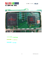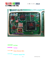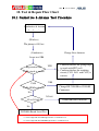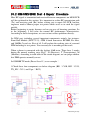
1
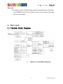
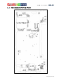
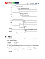
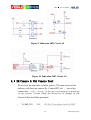
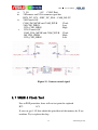
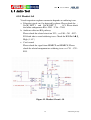
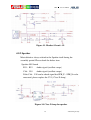
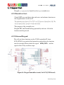
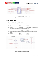
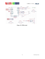
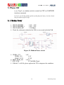
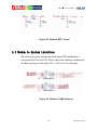
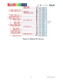
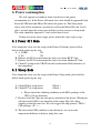
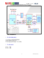
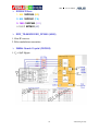
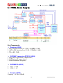
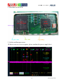
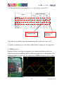
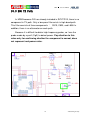
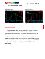
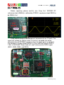
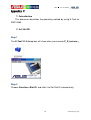
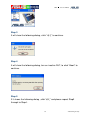
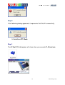
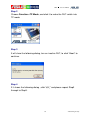
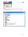
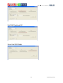
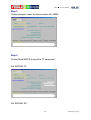
華碩電腦
GTC
■ Service Manual
ASUS M930 Level 3 4 Trouble
shooting Guide
Ver 1.0
1
ASUS Proprietary
華碩電腦
GTC
■ Service Manual
CONTENT
1.
OVER VIEW............................................................................................... 5
1.1 SYSTEM BLOCK DIAGRAM ............................................................................ 5
1.2 POWER DOMAIN BLOCK .............................................................................. 6
1.3 PLACEMENT TOP VIEW ............................................................................... 7
1.4 PLACEMENT BOTTOM VIEW ......................................................................... 8
1.5 SPECIFICATION ............................................................................................. 9
2.
SYSTEM CAN’T BOOT ......................................................................... 10
3.1 POWER-ON SEQUENCE ................................................................................ 10
1.2 OTHERS...................................................................................................... 11
3.
MMI TEST ITEM .................................................................................... 13
4.1 MICRO SD TEST......................................................................................... 13
4.2 SIM TEST .................................................................................................. 13
4.3 DISPLAY TEST ............................................................................................ 14
4.4 VIBRATOR TEST ......................................................................................... 15
4.5 LED TEST .................................................................................................. 15
2.5.1 RGB Led fail ..................................................................................... 15
2.5.2 Keypad LED fail ................................................................................ 15
4.6 2M CAMERA & VGA CAMERA TEST ......................................................... 16
4.7 SDRAM & FLASH TEST ............................................................................ 17
4.8 AUDIO TEST ............................................................................................... 18
4.8.1 Headset fail........................................................................................ 18
4.8.2 Speaker .............................................................................................. 19
4.8.3 On-Board Microphone can’t record ................................................. 20
4.8.4 Receiver ............................................................................................. 20
4.9 KEYPAD TEST ............................................................................................ 21
4.9.1 Board level test:................................................................................. 21
4.9.2 External Keypad ................................................................................ 21
4.9.3 Internal Qwerty Keypad .................................................................... 22
4.10 BT TEST .................................................................................................. 22
4.11 WIFI TEST ............................................................................................... 23
2
ASUS Proprietary
華碩電腦
GTC
■ Service Manual
5. PHONE OFF ................................................................................................. 25
5.1 MODEM POWER ......................................................................................... 25
5.2 MODEM TO SYSTEM INTERFACE ................................................................. 26
6. POWER CONSUMPTION ......................................................................... 28
6.1 POWER OFF MODE ..................................................................................... 28
6.2 SLEEP MODE .............................................................................................. 28
7. RF REPAIR REQUIREMENT................................................................... 29
7.1 SOFTWARE REQUIREMENTS:.................................................................... 29
7.2 HARDWARE REQUIREMENTS: .................................................................. 29
7.3 EQUIPMENT ............................................................................................... 29
8. BLOCK DIAGRAM..................................................................................... 30
8.1 RF BLOCK DIAGRAM OF VEGA2 .............................................................. 30
8.3 WCDMA BLOCK DIAGRAM ...................................................................... 33
9. GSM & WCDMA RF TX/RX PATH ......................................................... 34
9.1 BACKSIDE ANTENNA AREA ....................................................................... 34
9.2 EGG TX/RX PATH ...................................................................................... 35
9.3 WCDMA TX/RX PATH .............................................................................. 36
10. TEST & REPAIR FLOW CHART .......................................................... 37
10.1 CONDUCTIVE & ANTENNA TEST PROCEDURE .......................................... 37
10.2 GSM/GPRS/EDGE TEST & REPAIR PROCEDURE ................................... 38
10.3 EGG TX PATH......................................................................................... 41
10.3.1 Probe ............................................................................................... 42
10.3.2 Placement on the PCB..................................................................... 42
10.3.3 Measurement Result ........................................................................ 43
10.4 EGG RX.................................................................................................. 45
10.5 GSM/GPRS/EDGE REPAIR PROCEDURE ................................................ 46
10.6 WCDMA TEST & REPAIR PROCEDURE ................................................... 47
10.7 WCDMA TX .......................................................................................... 48
10.8 WCDMA RX .......................................................................................... 53
10.9 WCDMA TEST & REPAIR PROCEDURE ................................................... 54
APPENDIX........................................................................................................ 55
3
ASUS Proprietary
華碩電腦
GTC
■ Service Manual
APPENDIX A .................................................................................................... 55
APPENDIX B..................................................................................................... 55
APPENDIX C..................................................................................................... 56
1. Introduction............................................................................................ 56
2. Set Slot ID............................................................................................... 56
3. Switch to TP Mode.................................................................................. 58
4. Operating Method .................................................................................. 61
4
ASUS Proprietary
華碩電腦
GTC
■ Service Manual
Forward
The purpose of the troubleshooting guide just implement for the failure
on the MMI Testing. We will show several cases to discuss the repair
reference procedure.
1. Over view
1.1 System block diagram
i.
Figure 1. System Block Diagram
5
ASUS Proprietary
華碩電腦
GTC
■ Service Manual
1.2 Power Domain Block
Figure 2. Power Block Diagram
6
ASUS Proprietary
華碩電腦
GTC
■ Service Manual
1.3 Placement TOP View
7
ASUS Proprietary
華碩電腦
GTC
■ Service Manual
1.4 Placement
Placement Bottom View
8
ASUS Proprietary
華碩電腦
GTC
■ Service Manual
1.5 Specification
9
ASUS Proprietary
華碩電腦
2. SYSTEM Can’t Boot
GTC
■ Service Manual
The main of the reason always focus on the component short and
incorrect Power-on Sequence. In personal opinion, the power consumption
of M930 can be check before the Power on Sequence. Please check the
Power consumption of the M930 via power supply in R&D comment. It
always judges SMT component defective issue: short, open. In general,
power range will below 1mA in the deep sleep mode (Not touch the Power
key of the device).
Please check the put low signal after we push the power key on the U32
pin 4.
3.1 Power
Powerower-on sequence
A. The signal VBAT = power supply voltage
The VBAT can make sure the system power effective. Please check
the voltage on the CON23 pin1.
B. V_CORE = 1.3~1.45, V_IO = 1.8,
The signal V_CORE and V_IO can make sure cpu power domain
from PMU. Please check the voltage and try to eliminate component
soldering issue (cold soldering, float mounting) on the below item:
R77、R19 / R202、R76、R72
C. V_PLL = 1.3,
Please check the voltage and try to eliminate component soldering
issue (cold soldering, float mounting) on the below item:
R20.
10
ASUS Proprietary
華碩電腦
GTC
■ Service Manual
Figure 3. Power On Sequence
1.2 Others
1.If all of the signal have checked and still not improve the status. Please
check the below signal.
C110.Pin1
32.768KHz
R151.Pin1&2
26MHz
2. Please check the insulation tape is well between VGA Camera and FPC
side. Please avoid the short issue.
3. If still can’t not improve the status, you should check the CPU and
Memory status by X-ray machine. We can try to replace the CPU and
memory which has updated the firmware with m930w reference
version.
11
ASUS Proprietary
華碩電腦
GTC
■ Service Manual
4.
Figure 4. PMU-01
Figure 5. PMU-02
12
ASUS Proprietary
華碩電腦
3. MMI Test item
GTC
■ Service Manual
4.1 Micro SD Test
The MMI test tool will be auto-executed by itself after we insert the
MMI Micro SD card. If the phone can’t get the data on the storage
device, we should check the pathway on below process.
A. V_MMC
3.0V, CON27 Pin4
B. SD_DET#
0V, R54 Pin1.
C.
If item A fail, try to check open or short issue on the PMU.
If item B fail, try to check the CON27 Pin13 & Pin14.In the general; it
will short when we put in the card. Please change the CON27 if the
Pin13 and Pin 14 not short.
Figure 6. MicroSD + SIM Circuit
4.2 SIM Test
If SIM test fail, please check below items.
A. SIM_VCC
2.85V
If not please check the open or short on U39.
B. Please check the connector 27 on touch issue.
13
ASUS Proprietary
華碩電腦
GTC
■ Service Manual
4.3 Display Test
The test item will focus LCM interface and backlight. If result is fail
please check below item.
A. VIO_LCD
1.8V,
R143 both side.
B. LCD_VSYNC
LCD_HSYNC
LCD_PCLK
video clock,
C238Pin1、C239Pin1、R111 both side on soldering issue.
C. If the main screen backlight wasn’t executed, we can check below
items on the LCD_PCB auxiliary board.
(LED_V+)
12.1V
MAIN_BL_EN
1.8V
If something wrong with the result which we found, please check U1
peripheral components and circuit.
D. If the secondary screen backlight wasn’t executed, we can check
below items on the LCD_PCB auxiliary board.
LED_V+
6.2V
SUB_BL_EN
1.8V
If something wrong with the result which we found, please check U1
peripheral components and circuit.
Figure 7. Backlight Driver Circuit ( On LCD_PCB board)
14
ASUS Proprietary
華碩電腦
GTC
■ Service Manual
4.4 Vibrator Test
If the vibrator can not working, please refer to below items try to
eliminate the error.
U17 Pin1
3.0V
PMU ( U31 )
open / short
Figure 8. Vibrator Circuit
4.5 LED Test
We can check the RGB LED function and keypad LED via this test
item. The indication LED will show: Red-> Green->Blue->kpd White
LED->Red…….etc.
2.5.1 RGB Led fail
1.
2.
3.
4.
Please check R1, R2, R3 on soldering status.
Check the Pin9 and Pin 10 on the U5.
If the answer is no, please check the open/short on the CPU.
Replace the LED1.
2.5.2 Keypad LED fail
If the keypad LED will not executed. We can check below items on
the LCD_PCB auxiliary board.
LED_V+
SUB_BL_EN
6.2V
1.8V (Figure 4 )
15
ASUS Proprietary
華碩電腦
GTC
■ Service Manual
Figure 9. Indication LED Circuit -01
Figure 10. Indication LED Circuit -02
4.6 2M Camera & VGA Camera Test
We also test the item after assembly process. The main reason of the
defective will focus on camera. Ex. Camera FPC fail 、 lens of the
camera dirty 、can’t focus. If the pre-view image also shacking
on the screen. Please check the defective or damage on the
Coaxial Cable and follow procedure.
i.
VCAM_2V8
2.8V,
C69 Pin1.If not please check the PMU.
16
ASUS Proprietary
華碩電腦
ii.
iii.
iv.
v.
GTC
■ Service Manual
V_IO
1.8V, CON2 Pin6
2M camera and VGA common signal bus
KEY_I2C_SCL、KEY_I2C_SDA、CAM_D0~D7
2M Camera ON
CAM_2M_MCLK and CAM_XCLK
Clock
2M_CLK_SHDN
Low
VGA_CLK_SHDN
High
VGA Camera ON
CAM_VGA_MCLK and CAM_XCLK Clock
2M_CLK_SHDN
High
VGA_CLK_SHDN
Low
Figure 11. Camera control signal
4.7 SDRAM & Flash Test
Due to POP procedure, there will not test point be explored.
R72
1.8V
If you can get 1.8V then check the open/short of the memory by X-ray
machine. Try to replace the chip.
17
ASUS Proprietary
華碩電腦
GTC
■ Service Manual
4.8 Audio Test
Test
4.8.1 Headset fail
Visual inspection earphone connector depends on soldering issue.
a. If headset signal can’t be detected by phone. Please check the ,
JACK_DET_1 and JACK_DET_2
1.8V. Please check
the below components:R36、R93、C56、C240.
b. Audio no effect on R/L pathway
Please check the related circuit on U12, , ex:C40、C41、R37、
R38 both side to avoid soldering issue. Check the R30 Pin2 是
High ( 1.8V )
c. Can’t record
Please check the signal from HSMICP and HSMICN, Please
check the related component on soldering issue. ex. C51、C52、
R35.
Figure 12. Headset Circuit - 01
18
ASUS Proprietary
華碩電腦
GTC
■ Service Manual
Figure 13. Headset Circuit - 02
4.8.2 Speaker
Most defective always related to the Speaker itself during the
assembly period. Please check the below item.
Speaker NO Sound
R31、R32
Audio signal (oscillate scope)
C46、C49
Audio signal (oscillate scope)
If the C46、C49 can be check signal but SPK_P、SPK_N no be
measured, please replace the U13 ( Class-D Amp).
Figure 14. Class D Amp for speaker
19
ASUS Proprietary
華碩電腦
GTC
■ Service Manual
4.8.3 On-Board Microphone can’t record
If recording quality is poor U15 NG.
If recording function is fail, please check R39、R44、C55、C60.
Figure 15. Microphone circuit
4.8.4 Receiver
If Receiver no voice, please check the C1、C2 on the LCD_FPC.
If still can’t find any signal , please check Soldering issue( open /
short) on the PMU.
Please replace the Receiver in the final step.
20
ASUS Proprietary
華碩電腦
GTC
■ Service Manual
4.9 Keypad Test
Keypad is constructed by board-level test and assembly test.
4.9.1 Board level test:
Check SMT issue and detect the each rows and columns function on
the keypad matrix via driver IC.
The pathway from driver IC to CPU via I2C protocol should be OK. We
can use specify key group to verify the result.
The purpose of the assembly test:
Keypad FPC and Touch Feeling operated by end user. All of the
buttons need be pressed.
4.9.2 External Keypad
We will use those functions on the U5 I/O controller IC from
LCD_PCB. If you can feel the button has pushed after the function
can not executed. Please check the signal KPD_INT# and the
signal of the U5 by oscillate scope.
Figure 16. Keypad controller circuit( On LCD_PCB board)
21
ASUS Proprietary
華碩電腦
GTC
■ Service Manual
4.9.3 Internal Qwerty Keypad
The signal control by U31. If you have any problem, try to check
soldering issue(Open / Short) by X-ray.
Figure 17. Qwerty Keypad controller circuit
4.10 BT Test
In general should be get follow bellow status
Check
C25
Visual inspection
R80、R86
Check
U55 Pin1
Pin9/Pin10 Short
Pin6/Pin7 Short
26MHz clock
Low
Figure 18. BT circuit
22
ASUS Proprietary
華碩電腦
GTC
■ Service Manual
Figure 19. BT UART switch circuit
4.11 WiFi Test
In general should be get follow bellow status
D. Check
R74
1.8V
E. Check
U10 Pin3
1.8V (High), If the result is
true please check the U10 on the soldering issue.
F. Check
U8 Pin3
1.8V (High)
Pin5
3.3V
G. Check the signal of the R29 will get the dynamic wave by oscillate
scope.
H. Check
R75
3.3V
R142
2.85V
Figure 20. WiFi PA Power circuit
23
ASUS Proprietary
華碩電腦
GTC
■ Service Manual
Figure 21. WiFi circuit
24
ASUS Proprietary
華碩電腦
5. Phone Off
GTC
■ Service Manual
In the Vega2, the modem switch is control by CPU via UART/SPI
interface command.
It won’t cut off the modem power in the physical layer, we also check
the procedure step by step:
5.1 Modem Power
1.
2.
3.
4.
VBAT_MODEM
3.6V ~ 4.2V
VBAT_MODEM_1
3.6V ~ 4.2V
VBAT_MOD_EN
1.8V(High)
Check the schematic related of the U40, try to rework with the U40.
Figure 22. Modem Power circuit
5. VDDD_1V5
1.5V
VDDE_1V8
1.8V
VDDC_2V75
2.75V
6. MOD_POW_ON
1.8V(?)
7. RTC_CLK
32.768 KHz Clock
8. If Item5~7 will Ok, please replace the U39 to improve the condition.
25
ASUS Proprietary
華碩電腦
GTC
■ Service Manual
Figure 23. Modem RTC circuit
5.2 Modem to System interface
The main inter phase which connected from CPU and Modem is
constructed by U58 and U59. Please check the soldering condition on
the BGA package of the chips(U58、U59) by X-ray detection.
Figure 24. Modem UART interface
26
ASUS Proprietary
華碩電腦
GTC
■ Service Manual
Figure 25. Modem/CPU interface
27
ASUS Proprietary
華碩電腦
6. Power consumption
GTC
■ Service Manual
We will support two mode to check our device in the power
consumption test. In the Power Off mode, the value should be approach 0 mA.
Insert the SIM card and Micro SD before the power on .The Sleep mode
active tool will be automatic executed by itself in the Micro SD card. It will
take 3 second when the screen turn to blend, system convert to sleep mode.
The value should be approach 2~3mA in the lowest level.
If there out of the above range, please check the value step by step:
6.1 Power Off Mode
If we found the value over the range in the Power Off mode, please follow
below check point step by step.
A. V_CORE
0V
V_IO
0V
B. Remove the R824 to determine the short issue from RF IC Side.
C. Remove the R125 to determine the short issue from Modem IC Side.
D. Check IC group on the VBAT network to determine Short defective of
the component.
6.2 Sleep Mode
If we found the value over the range in the Power Sleep mode, please follow
below check point step by step.
A. Check R76 by Amp meter.
B. Check R77 by Amp meter.
250uA↓
150uA↓
a. Please check the soldering condition on the BGA package of the
CPU by X-ray detection.
C. Review all of the Chips on each power network of the device. Which part
will short with GND is our direction of the repair. But still a huge
working to find the root cost. We will suggest the chip priority : BGA /
CSP package→IC→…..
D. The short with GND condition is not obviously, we can use the
temperature different to help us judge that soon.
28
ASUS Proprietary
華碩電腦
7. RF Repair requirement
GTC
■ Service Manual
7.1 Software requirements
requirements:
uirements:
U250_U360_E_Tool
Modem Firmware:Latest Version(include:APP and ACC GDFS File)
7.2 Hardware requirements:
requirements:
RF Connector and RF cable
High Frequency Probe with DC Block
(connect with a 0603 1µF capacitor)
Power Supply Contact
7.3 Equipment:
PC
Test Fixture
Oscilloscope
Communication tester:Agilent 8960, CMU200 or Anritsu 8820
Digital Multi Meter
Power Supply
Spectrum Analyzer (up to 3.0 GHz)
29
ASUS Proprietary
華碩電腦
8. Block Diagram
GTC
■ Service Manual
8.1 RF Block Diagram of VEGA2
7
3
EGG
4-band
SAW
4
MCLK
WB+EGG
4
4-band EGG
Digital BB
Transceiver
MCLKREQ Controller
RF 3000
DB 3150
8
2
EGG ANT
EGG Front-End
with WB Switch
SKY77513
2
XO(26MHz)
WBCLK
WBTX_IQ 4
WBRX_IQ 4
WB ANT
PD
Duplex
Isolator
DC/DC
Converter
WB PA
SKY77174
RX SAW
VDIGRAD_1V8
VDD_E
TX
SAW
2
30
WCDMA
Transceiver
RF 3100
LDO
(Option)
VDD_A
Analog BB
Controller
AB 3000
ASUS Proprietary
華碩電腦
GTC
■ Service Manual
8.2 GSM/GPRS/EDGE(EGG) Block Diagram
1.8V
Key Components
TX- RX FEM (U801)
1. Quad-Band GSM/GPRS/EDGE
2. Polar EDGE modulation
3. Low input power range ~ 0 to 6 dBm
Tx attenuator
1.U811:5dB
2.U810:4dB
31
ASUS Proprietary
華碩電腦
GTC
■ Service Manual
RXSAW Filters
1. 850:
:BPF800 (BG)
2. 900:
:BPF801 (TA)
3. 1800:
:BPF803 (SW)
4.1900:
:BPF802 (LF)
RFIF_TRANSCEIVER_RF3000 (U800)
1. Zero-IF receiver
2. Polar modulation transmitter
26MHz Quartz Crystal (OSC800)
1. CL=15pF 10ppm
32
ASUS Proprietary
華碩電腦
GTC
■ Service Manual
8.3 WCDMA Block Diagram
Key Components
Duplexer (U900)
1. TX to ANT Insertion Loss (1920...1980MHz) 1.2dB
2. ANT to RX: Insertion Loss (2110...2170MHz) 1.9dB
3. TX to RX: 57dB
WCDMA Transceiver RF3100 (U906)
1. Single band application (UMTS band1)
2. 3GPP release 5, power class 3
3. Zero Intermediate Frequency
WCDMA PA (U903)
1. VCC:2.75V
2. VDD:1.8V
Coupler (U905)
Coupling:19.30 ± 1.00 dB
33
ASUS Proprietary
華碩電腦
GTC ■ Service Manual
9. GSM & WCDMA RF Tx/Rx Path
9.1 Backside Antenna Area
GSM Antenna
WCDMA
Antenna Feed
34
ASUS Proprietary
華碩電腦
GTC
■ Service Manual
9.2 EGG TX/RX Path
Tx LB Path
Tx HB Path
Rx Path
35
ASUS Proprietary
華碩電腦
GTC
■ Service Manual
9.3 WCDMA TX/RX Path
Rx Path
Tx Path
Power Detector Path
PA power supply Path
36
ASUS Proprietary
華碩電腦
GTC ■ Service Manual
10. Test & Repair Flow Chart
10.1
10.1 Conductive & Antenna Test Procedure
Conductive & Antenna
Test Procedure
(Wireless)
The phone is ON, but
(Conductive)
Change New Antenna
Insert test SIM
YES
Registration OK
Tx/Rx signal is normal
1. Confirm whether the spring keeps
in touch with FPC well.
2. Confirm whether the matching
circuit (C823, L811 and C822) is
correct.
YES
U801
Change RF CON900 or CON800
Connector)
Tx/Rx FEM work well
No
2G fail
2G or 3G fail
GSM/GPRS/EDGE Board
No
WCDMA Board Level Test
:Refer to appendix A for EGG typical values of conductive test
*2:Refer to appendix B for WCDMA typical values of conductive test
37
*1
ASUS Proprietary
華碩電腦
GTC
■ Service Manual
10.2 GSM/GPRS/EDGE
GSM/GPRS/EDGE Test & Repair Procedure
How RF signal is transmitted and received between components on M930 PCB
will be explained in this section. It is important to realize RF transmission path
(Tx) and receiving path (Rx) before starting out to repair NG PCB, because
engineers need to choose proper test points which assist us to catch the signal
quickly
Before beginning to repair, because we have no way of knowing questions. So
in the beginning, I will refer the normal RF performance characteristics.
According to these descriptions, we can sort out various problems directly.
In GSM part, including several important components mainly, for instance:
Front End Module (SKY77513), GSM 4-band transceiver RF3000, Rx filter,
and 26MHz Crystal etc. First of all, I will explain the working state of a normal
FEM including its test points. You can analysis it according to the result.
When a phone is connected with the Agilent 8960 tester, There have 3 modes
during the normal working state (Fig1):R (Receiver), T (Transmission), M
(Monitor). According to truth table of the circuit diagram, we can judge whether
this FEM operates normally or not.
In GSM900 TX mode (Power Level 5 ) as an example:
1.Check these four components on below diagram (BS1:C830, BS2:C825,
TX_EN:C831, and Vapc:R822)
38
ASUS Proprietary
華碩電腦
GTC
■ Service Manual
2. Placement on the PCB
3. On the oscilloscope screen
(If there is not any wave to appear, please confirm the power supply first)
39
ASUS Proprietary
華碩電腦
GTC
■ Service Manual
4. Truth table of the circuit diagram (‘1’ is 1.8V & ‘0’ is near 0.2V)
Transmission
Receiver &
Monitor
Vapc only exists during that time transmitting (the value can’t over 1.5V).
5. Finally, according to its state form, which kind of wrong we can judge first.
6. 26MHz Crystal
Suppose if there is no signal to appear, first, confirm whether crystal is on
normal operation. In addition, because add an electric wire at this moment and
influence whole CL of crystal, the value is not 26MHz definitely, but it’s near.
40
ASUS Proprietary
華碩電腦
GTC
■ Service Manual
10.3 EGG TX Path
In M930 because PA has already included in SKY77513, there is no
component in TX path. Only a low-pass filter exists in high band path.
This filter consists of three components : C819, C820, and L808. In
addition, there is an attenuator on each path.
Because it is difficult to obtain high-frequency probe, so I use the
probe made by myself (Fig2) to detect power. Pay attention to this
value only for confirming whether the component is normal, does
not represent real power value.
41
ASUS Proprietary
華碩電腦
GTC
■ Service Manual
10.3.1 Probe
0603 1µF/16V
A 0603 1µF/16V
Capacitor
Fig2
10.3.2 Placement on the PCB
42
ASUS Proprietary
華碩電腦
GTC
■ Service Manual
10.3.3 Measurement Result
EGSM900 Ch62
DCS1800 Ch700
Pay attention to this value only for confirming whether the component is normal, does not
represent real power value.
From reading the value, we can judge from it whether their wave
and relative value are correct or not. In accordance with the
specifications of the probe used, the value of measurement is also not
the same.
First, waveforms must be a normal bust, and low band should
higher than high band about 1dB. This can only be confirmed TR switch
is in normal operation, not guarantee PA normal operation in SKY77513.
Need to confirm the value of Vapc, to find that FEM or TR is
problematic.
43
ASUS Proprietary
華碩電腦
GTC
■ Service Manual
Enlarge the TX of Fig2(振幅:amplitude & 寬度:width)
Range of Vapc is as follows:
1.
Low band 850/EGSM
:PL5
Vapc=1.29(V)
~ PL19
Vapc=0.27( V )
2.
High band 1800/1900
:PL0
Vapc=1.28(V)
~ PL 15
Vapc=0.26( V )
44
ASUS Proprietary
華碩電腦
GTC
■ Service Manual
10.4 EGG RX
Because there are only four filters on RX path, so when the
question happens, confirm the exactness of the packaging on filter at
first. Later, according to RX of Fig1, confirmed that operation was normal,
and observe the frequency of crystal is working or not.
Rx Filter packaging is as follows:
1.
BG:850
2.
TA:900
3.
LF:1900
4.
SW:1800
45
ASUS Proprietary
華碩電腦
GTC
■ Service Manual
10.5 GSM/GPRS/EDGE
GSM/GPRS/EDGE Repair Procedure
EGG Board Level
Check relevant components on
the path
Repair Procedure
Check
1. C826 is 3.8V
2. C802 is 2.75V and C805 is
1.8V
3. R828 has 26MHz
No
FEM has R、T、M
waveforms
YES
Rx
Check the four Rx filter
Tx or Rx path fail
Tx
U811 (low band) should
higher than U810 (high
band) about 1dB
YES
Check range of Vapc:
Low band 0.25(PL19) ~ 1.3V
(PL5)
No
No
Check U811, U810, andU800
Check U801 (SKY77513)
Restart EGG Board Level Repair
Procedure
Recalibration
46
ASUS Proprietary
華碩電腦
GTC
■ Service Manual
10.6 WCDMA Test & Repair Procedure
WCDMA part in M930i, only support band1, its component is much
more than EGG part. The main component is as follows, PA, duplexer,
TX filter, RX filter, coupler, isolator, and RF3100 etc. WCDMA uses code
to distinguish user, each user uses the same frequency, so especially
need to pay attention to the control of power. And then, I will use the
same analytical method of EGG.
The same as EGG, we observe the state of FEM first. Because
WCDMA does not make FDD, there are no R, T, M phenomenon to take
place.
Take WCDMA as an example:
When already connecting to communication tester. No matter TX or
RX are the same.
Both of BS1 and TX_EN are low, only BS2 is high ( ‘1 ’ is 1.8V).
47
ASUS Proprietary
華碩電腦
GTC
■ Service Manual
10.7 WCDMA TX
Before repairing, please confirm one thing first. WCDMA RF
reference clock (26MHz) is offered by RF3000, so please check R800 to
be 26MHz first.
26MH
Then, we will analysis the component characteristic on TX path; The
signal will include its relative value. First of all, we probe into some
characteristics of WCDMA transceiver first. Its power parts are divided
into two parts: Analog (check R909 is 2.75V) and Digit (check R919 is
1.8V). In WCDMA TX part, both of I and Q channel are QPSK signal
(R921, R923, R925, and R929).
48
ASUS Proprietary
華碩電腦
GTC
■ Service Manual
Using probe (Fig2) to check TX SAW Filter output (R912), can see a
WCDMA signal. Pay attention to the value only for confirming
whether the component is normal, does not represent real power
value.
Check PA output (C927(it’s a resistor R))
Conductive Power is 23dBm (CON900)
PA Gain Condition: In high power mode is more than 27dB.
49
ASUS Proprietary
華碩電腦
GTC
■ Service Manual
Check Duplexer output (R920)
Pay attention to this value only for confirming whether the component is normal, does not
represent real power value.
In TX part, the main components are all passive, except PA and
RF3100. So must especially discuss the operation principle of PA finally.
This is divided into two parts:One is power supplied and the other is
power detector.
DC/DC converter is used to reduce WCDMA power consumption.
VCC _ PA is divided into two pieces of power:One is VCC1 (3.15V) for
driving amplifier and the other is VCC2 (3.15V) for power amplifier.
50
ASUS Proprietary
華碩電腦
GTC
■ Service Manual
RF3100 has two RF _ DAC must be paid attention to:RF_DAC1
and RF_DAC2. DAC1 gives PA, and DAC2 gives DC/DC converter. In
23dBm, both of DAC1 (R910) and DAC2 (R905) are all 1.27 V;In
11dBm, DAC1 is 670mV and DAC2 is 570mV.
Power detector is used to feedback power to DB3150, to transmitter
correct wanted power.
U910
51
ASUS Proprietary
華碩電腦
GTC
■ Service Manual
Check WPOW_SENSE (U910 input) = PA output power - 20dBm :
Coupling is 20dB.
Check power detector output (R904) = WPOW_SENSE – 15dBm :
Attenuator is 15dB.
52
ASUS Proprietary
華碩電腦
GTC
■ Service Manual
10.8 WCDMA RX
Finally, we will analysis the RX characteristic. In WCDMA RX part,
both of I and Q channel are HPSK signal (R924, R926, R930, and R931).
On RX path, only one RX filter is external. It has a LNA (16dB) within
RF3100 that amplifies the RX signal.
Because the strength of RX signal is too small, so spectrum must
have some extra setup. In order to observe the signal easily, must
strengthen BCH to - 30dBm.
Check MIX1 input (L900)
53
ASUS Proprietary
華碩電腦
GTC
■ Service Manual
10.9 WCDMA Test & Repair Procedure
Check relevant components on
WCDMA Board Level
Repair Procedure
FEM has waveforms
R920 has power
Check
1. C905 and L901 are 3.15V
2. R909, R900 are 2.75V and R919 is 1.8V
3. R800 is 26MHz
No
YES
Tx or Rx path fail
Rx
Check L900 and RX filter
Tx
Change U906 RF3100
Check R912 power
YES
YES
Check U905, U904, and U900 by
relationship.
Check C927 power
No
PA output has power YES
normal
No
Check power detector system (U910 and
Check power supply system (R905 and
Restart WCDMA Board Level Repair
Procedure
Recalibration
54
ASUS Proprietary
華碩電腦
Appendix
GTC
■ Service Manual
Appendix A
Appendix B
Band
WCDMA
ARFCN
9612
9750
9888
Conductive Power(dBm)
23.5
23.5
23.5
55
ASUS Proprietary
華碩電腦
GTC
■ Service Manual
Appendix C
1. Introduction
This document describes the operating method by using E-Tool for
EMP U360.
2. Set Slot ID
Step 1
The E-Tool V1.0 dialog box will show when you execute P_E_tool.exe.
Step 2
Choose Function->Slot ID, and click it to Set Slot ID automatically.
56
ASUS Proprietary
華碩電腦
GTC
■ Service Manual
Step 3
It will show the following dialog , click “確定” to continue.
Step 4
It will show the following dialog, turn on inactive DUT, to click “Abort” to
continue.
Step 5
If it shows the following dialog , click“確定” and please repeat Step2
through to Step4 .
57
ASUS Proprietary
華碩電腦
GTC
■ Service Manual
Step 6
If the following dialog appeared, it represents Set Slot ID successfully.
3. Switch to TP Mode
Step 1
The E-Tool V1.0 dialog box will show when you execute P_E_tool.exe.
58
ASUS Proprietary
華碩電腦
GTC
■ Service Manual
Step 2
Choose Function->TP Mode, and click it to make the DUT switch into
TP mode.
Step 3
It will show the following dialog, turn on inactive DUT, to click “Abort” to
continue.
Step 4
If it shows the following dialog , click“確定” and please repeat Step2
through to Step3.
59
ASUS Proprietary
華碩電腦
GTC
■ Service Manual
Step 4
If the following dialog appeared, it represents DUT switched into TP
mode successfully.
60
ASUS Proprietary
華碩電腦
GTC
■ Service Manual
4. Operating Method
GSM PART
Step 1
The E-Tool V1.0 dialog box will show when you execute P_E_tool.exe.
Step 2
Choose Function->U360->GSM, and click GSM to show
GSM_U360_form dialog box.
Step 3
61
ASUS Proprietary
華碩電腦
GTC
■ Service Manual
Choice comport number to communicate with M930 (seen by computer).
Step 4
Chose which TP command to send
Set GSM Static TX
Set GSM Switched TX
Set GSM Static RX
62
ASUS Proprietary
華碩電腦
GTC
■ Service Manual
Set GSM Switched RX
Reset the GSM Radio
63
ASUS Proprietary
華碩電腦
GTC
■ Service Manual
WCDMA PART
Step 1
The E-Tool V1.0 dialog box will show when you execute P_E_tool.exe.
Step 2
Choose Finction->U360->WCDMA, and click WCDMA to show
WCDMA_U360_form dialog box.
64
ASUS Proprietary
華碩電腦
GTC
■ Service Manual
Step 3
Choice comport umber to communicate with M930.
Step 4
Choice Band MODE to send the TP command
Set WCDMA TX
Set WCDMA RX
65
ASUS Proprietary
華碩電腦
GTC
■ Service Manual
POWER Sense ADC Read
Result is showed as below
66
ASUS Proprietary
華碩電腦
GTC
■ Service Manual
Step 5
Reset WCDMA Radio
67
ASUS Proprietary