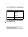
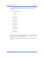
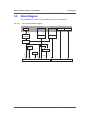
1
CPCI-6115 CompactPCI
Single Board Computer
Installation and Use
6806800A68D
March 2008
©
Copyright 2008, 2007, 2006 Motorola, Inc.
All rights reserved.
Printed in the United States of America.
Trademarks
Motorola® and the Motorola symbol are registered trademarks of Motorola, Inc.
CompactPCI® is a registered trademark of PCI Industrial Computer Manufacturers Group.
All other product or service names mentioned in this document are trademarks or registered trademarks of their respective holders.
Notice
While reasonable efforts have been made to assure the accuracy of this document, Motorola, Inc. assumes no liability resulting from
any omissions in this document, or from the use of the information obtained therein. Motorola reserves the right to revise this document
and to make changes from time to time in the content hereof without obligation of Motorola to notify any person of such revision or
changes.
Electronic versions of this material may be read online, downloaded for personal use, or referenced in another document as a URL to
the Motorola Computer Group Web site. The text itself may not be published commercially in print or electronic form, edited, translated,
or otherwise altered without the permission of Motorola, Inc.
It is possible that this publication may contain reference to or information about Motorola products (machines and programs),
programming, or services that are not available in your country. Such references or information must not be construed to mean that
Motorola intends to announce such Motorola products, programming, or services in your country.
Limited and Restricted Rights Legend
If the documentation contained herein is supplied, directly or indirectly, to the U.S. Government, the following notice shall apply unless
otherwise agreed to in writing by Motorola, Inc.
Use, duplication, or disclosure by the Government is subject to restrictions as set forth in subparagraph (b)(3) of the Rights in Technical
Data clause at DFARS 252.227-7013 (Nov. 1995) and of the Rights in Noncommercial Computer Software and Documentation clause
at DFARS 252.227-7014 (Jun. 1995).
Motorola, Inc.
Embedded Communications Computing
2900 South Diablo Way, Suite 190
Tempe, Arizona 85282
Contents
About this Manual . . . . . . . . . . . . . . . . . . . . . . . . . . . . . . . . . . . . . . . . . . . . . . . . . . . . . . . . . . . . . . . . . . 11
Safety Notes. . . . . . . . . . . . . . . . . . . . . . . . . . . . . . . . . . . . . . . . . . . . . . . . . . . . . . . . . . . . . . . . . . . . . . . 17
Sicherheitshinweise . . . . . . . . . . . . . . . . . . . . . . . . . . . . . . . . . . . . . . . . . . . . . . . . . . . . . . . . . . . . . . . . 21
1
Introduction . . . . . . . . . . . . . . . . . . . . . . . . . . . . . . . . . . . . . . . . . . . . . . . . . . . . . . . . . . . . . . . . . . . . 25
1.1
1.2
1.3
2
Features . . . . . . . . . . . . . . . . . . . . . . . . . . . . . . . . . . . . . . . . . . . . . . . . . . . . . . . . . . . . . . . . . . 25
Standard Compliances . . . . . . . . . . . . . . . . . . . . . . . . . . . . . . . . . . . . . . . . . . . . . . . . . . . . . . . 26
Ordering Information . . . . . . . . . . . . . . . . . . . . . . . . . . . . . . . . . . . . . . . . . . . . . . . . . . . . . . . . . 27
Hardware Preparation and Installation . . . . . . . . . . . . . . . . . . . . . . . . . . . . . . . . . . . . . . . . . . . . . . 29
2.1
2.2
2.3
2.4
2.5
2.6
2.7
2.8
2.9
Overview . . . . . . . . . . . . . . . . . . . . . . . . . . . . . . . . . . . . . . . . . . . . . . . . . . . . . . . . . . . . . . . . . .
Unpacking and Inspecting the Board . . . . . . . . . . . . . . . . . . . . . . . . . . . . . . . . . . . . . . . . . . . .
Environmental, Power, and Thermal Requirements . . . . . . . . . . . . . . . . . . . . . . . . . . . . . . . . .
2.3.1 Environmental Requirements . . . . . . . . . . . . . . . . . . . . . . . . . . . . . . . . . . . . . . . . . . . . .
2.3.2 Power Requirements . . . . . . . . . . . . . . . . . . . . . . . . . . . . . . . . . . . . . . . . . . . . . . . . . . .
2.3.3 Thermal Requirements. . . . . . . . . . . . . . . . . . . . . . . . . . . . . . . . . . . . . . . . . . . . . . . . . .
Getting Started . . . . . . . . . . . . . . . . . . . . . . . . . . . . . . . . . . . . . . . . . . . . . . . . . . . . . . . . . . . . .
2.4.1 Overview of Start-up Procedure . . . . . . . . . . . . . . . . . . . . . . . . . . . . . . . . . . . . . . . . . . .
2.4.2 Equipment Required. . . . . . . . . . . . . . . . . . . . . . . . . . . . . . . . . . . . . . . . . . . . . . . . . . . .
Baseboard Preparation . . . . . . . . . . . . . . . . . . . . . . . . . . . . . . . . . . . . . . . . . . . . . . . . . . . . . . .
2.5.1 Configuring the Hardware . . . . . . . . . . . . . . . . . . . . . . . . . . . . . . . . . . . . . . . . . . . . . . .
2.5.2 Setting Switches and Jumpers . . . . . . . . . . . . . . . . . . . . . . . . . . . . . . . . . . . . . . . . . . . .
2.5.3 J6, Bus Mode Selection . . . . . . . . . . . . . . . . . . . . . . . . . . . . . . . . . . . . . . . . . . . . . . . . .
2.5.4 J9, Standalone Operating Mode. . . . . . . . . . . . . . . . . . . . . . . . . . . . . . . . . . . . . . . . . . .
2.5.5 J10, Flash Bank Selection . . . . . . . . . . . . . . . . . . . . . . . . . . . . . . . . . . . . . . . . . . . . . . .
2.5.6 J15, +/-12 V Present Header . . . . . . . . . . . . . . . . . . . . . . . . . . . . . . . . . . . . . . . . . . . . .
2.5.7 J20, Safe Start Header. . . . . . . . . . . . . . . . . . . . . . . . . . . . . . . . . . . . . . . . . . . . . . . . . .
2.5.8 J25, SROM Initialization Enable Header . . . . . . . . . . . . . . . . . . . . . . . . . . . . . . . . . . . .
2.5.9 J99, Flash Bank A Programming Enable Header. . . . . . . . . . . . . . . . . . . . . . . . . . . . . .
2.5.10 SW2, Geographic Address. . . . . . . . . . . . . . . . . . . . . . . . . . . . . . . . . . . . . . . . . . . . . . .
Operating Modes . . . . . . . . . . . . . . . . . . . . . . . . . . . . . . . . . . . . . . . . . . . . . . . . . . . . . . . . . . .
Installing Hardware . . . . . . . . . . . . . . . . . . . . . . . . . . . . . . . . . . . . . . . . . . . . . . . . . . . . . . . . . .
2.7.1 Installing PMC Modules on the CPCI-6115 . . . . . . . . . . . . . . . . . . . . . . . . . . . . . . . . . .
2.7.2 Installing the CPCI-6115 Baseboard . . . . . . . . . . . . . . . . . . . . . . . . . . . . . . . . . . . . . . .
Connecting to a Console Port . . . . . . . . . . . . . . . . . . . . . . . . . . . . . . . . . . . . . . . . . . . . . . . . . .
Applying Power . . . . . . . . . . . . . . . . . . . . . . . . . . . . . . . . . . . . . . . . . . . . . . . . . . . . . . . . . . . . .
CPCI-6115 CompactPCI Single Board Computer Installation and Use (6806800A68D)
29
29
30
30
32
32
35
35
36
36
36
37
38
39
39
40
40
41
41
42
42
42
43
46
47
47
1
Contents
3
Controls, LEDs, and Connectors. . . . . . . . . . . . . . . . . . . . . . . . . . . . . . . . . . . . . . . . . . . . . . . . . . . 49
3.1
3.2
3.3
3.4
3.5
4
49
50
50
52
52
52
53
53
54
54
55
56
57
59
63
63
64
64
65
65
65
66
66
Functional Description . . . . . . . . . . . . . . . . . . . . . . . . . . . . . . . . . . . . . . . . . . . . . . . . . . . . . . . . . . . 67
4.1
4.2
4.3
2
Overview . . . . . . . . . . . . . . . . . . . . . . . . . . . . . . . . . . . . . . . . . . . . . . . . . . . . . . . . . . . . . . . . . .
Board Layout . . . . . . . . . . . . . . . . . . . . . . . . . . . . . . . . . . . . . . . . . . . . . . . . . . . . . . . . . . . . . . .
Front Panel Connectors and LEDs . . . . . . . . . . . . . . . . . . . . . . . . . . . . . . . . . . . . . . . . . . . . . .
ABORT/Reset Switch . . . . . . . . . . . . . . . . . . . . . . . . . . . . . . . . . . . . . . . . . . . . . . . . . . . . . . . .
On-Board Connectors and Headers . . . . . . . . . . . . . . . . . . . . . . . . . . . . . . . . . . . . . . . . . . . . .
3.5.1 J19, Front Panel Asynchronous Serial Port . . . . . . . . . . . . . . . . . . . . . . . . . . . . . . . . . .
3.5.2 J95, Front Panel 10/100/1000 Megabits/s Ethernet Connector . . . . . . . . . . . . . . . . . . .
3.5.3 CompactPCI J1/J2 Connectors . . . . . . . . . . . . . . . . . . . . . . . . . . . . . . . . . . . . . . . . . . .
3.5.4 CompactPCI Bus Connector . . . . . . . . . . . . . . . . . . . . . . . . . . . . . . . . . . . . . . . . . . . . .
3.5.5 CompactPCI Bus Connector . . . . . . . . . . . . . . . . . . . . . . . . . . . . . . . . . . . . . . . . . . . . .
3.5.6 CompactPCI User I/O Connector . . . . . . . . . . . . . . . . . . . . . . . . . . . . . . . . . . . . . . . . . .
3.5.7 CompactPCI Connector . . . . . . . . . . . . . . . . . . . . . . . . . . . . . . . . . . . . . . . . . . . . . . . . .
3.5.8 CompactPCI User I/O Connector . . . . . . . . . . . . . . . . . . . . . . . . . . . . . . . . . . . . . . . . . .
3.5.9 PCI Mezzanine Card (PMC) Connectors . . . . . . . . . . . . . . . . . . . . . . . . . . . . . . . . . . . .
3.5.10 Boundary Scan JTAG Header . . . . . . . . . . . . . . . . . . . . . . . . . . . . . . . . . . . . . . . . . . . .
3.5.11 Processor JTAG/COP Header . . . . . . . . . . . . . . . . . . . . . . . . . . . . . . . . . . . . . . . . . . . .
3.5.12 Stand-Alone Operation Select Header . . . . . . . . . . . . . . . . . . . . . . . . . . . . . . . . . . . . . .
3.5.13 Flash Boot Bank Select Header . . . . . . . . . . . . . . . . . . . . . . . . . . . . . . . . . . . . . . . . . . .
3.5.14 Safe Start Header. . . . . . . . . . . . . . . . . . . . . . . . . . . . . . . . . . . . . . . . . . . . . . . . . . . . . .
3.5.15 Bus Mode Select Header . . . . . . . . . . . . . . . . . . . . . . . . . . . . . . . . . . . . . . . . . . . . . . . .
3.5.16 SROM Initialization Enable Header . . . . . . . . . . . . . . . . . . . . . . . . . . . . . . . . . . . . . . . .
3.5.17 Flash Bank A Write Protect Header . . . . . . . . . . . . . . . . . . . . . . . . . . . . . . . . . . . . . . . .
3.5.18 +/-12 V Present Header . . . . . . . . . . . . . . . . . . . . . . . . . . . . . . . . . . . . . . . . . . . . . . . . .
Overview . . . . . . . . . . . . . . . . . . . . . . . . . . . . . . . . . . . . . . . . . . . . . . . . . . . . . . . . . . . . . . . . . .
Block Diagram . . . . . . . . . . . . . . . . . . . . . . . . . . . . . . . . . . . . . . . . . . . . . . . . . . . . . . . . . . . . . .
General Description . . . . . . . . . . . . . . . . . . . . . . . . . . . . . . . . . . . . . . . . . . . . . . . . . . . . . . . . .
4.3.1 Processor Bus Resources . . . . . . . . . . . . . . . . . . . . . . . . . . . . . . . . . . . . . . . . . . . . . . .
4.3.2 Processor . . . . . . . . . . . . . . . . . . . . . . . . . . . . . . . . . . . . . . . . . . . . . . . . . . . . . . . . . . . .
4.3.3 L3 Cache . . . . . . . . . . . . . . . . . . . . . . . . . . . . . . . . . . . . . . . . . . . . . . . . . . . . . . . . . . . .
4.3.4 MV64360 System Controller . . . . . . . . . . . . . . . . . . . . . . . . . . . . . . . . . . . . . . . . . . . . .
4.3.4.1 MV64360 CPU Bus Interface . . . . . . . . . . . . . . . . . . . . . . . . . . . . . . . . . . . . .
4.3.4.2 MV64360 DDR SDRAM Interface . . . . . . . . . . . . . . . . . . . . . . . . . . . . . . . . .
4.3.4.3 MV64360 32-bit Interface to Devices . . . . . . . . . . . . . . . . . . . . . . . . . . . . . . .
4.3.4.4 MV64360 Dual PCI/PCI-X Interfaces . . . . . . . . . . . . . . . . . . . . . . . . . . . . . . .
4.3.4.5 MV64360 Integrated Gigabit Ethernet MACs . . . . . . . . . . . . . . . . . . . . . . . . .
4.3.4.6 MV64360 Integrated 2 Megabit SRAM . . . . . . . . . . . . . . . . . . . . . . . . . . . . . .
4.3.4.7 MV64360 General-Purpose 32-bit Timer/Counters . . . . . . . . . . . . . . . . . . . .
4.3.4.8 MV64360 Watchdog Timer . . . . . . . . . . . . . . . . . . . . . . . . . . . . . . . . . . . . . . .
4.3.4.9 MV64360 I2O Message Unit . . . . . . . . . . . . . . . . . . . . . . . . . . . . . . . . . . . . .
4.3.4.10 MV64360 Four-Channel Independent DMA Controller . . . . . . . . . . . . . . . . .
4.3.4.11 MV64360 I2C Interface . . . . . . . . . . . . . . . . . . . . . . . . . . . . . . . . . . . . . . . . .
4.3.4.12 Interrupt Controller . . . . . . . . . . . . . . . . . . . . . . . . . . . . . . . . . . . . . . . . . . . . .
67
68
69
69
70
70
70
71
71
72
72
72
73
73
73
73
73
73
74
CPCI-6115 CompactPCI Single Board Computer Installation and Use (6806800A68D)
Contents
4.4
5
4.3.4.13 PCI Bus Arbitration . . . . . . . . . . . . . . . . . . . . . . . . . . . . . . . . . . . . . . . . . . . . .
4.3.4.14 Board Reset Logic . . . . . . . . . . . . . . . . . . . . . . . . . . . . . . . . . . . . . . . . . . . . .
4.3.4.15 MV64360 MPP Configuration . . . . . . . . . . . . . . . . . . . . . . . . . . . . . . . . . . . . .
4.3.4.16 MV64360 Reset Configuration . . . . . . . . . . . . . . . . . . . . . . . . . . . . . . . . . . . .
4.3.5 System Memory . . . . . . . . . . . . . . . . . . . . . . . . . . . . . . . . . . . . . . . . . . . . . . . . . . . . . . .
4.3.6 Flash Memory. . . . . . . . . . . . . . . . . . . . . . . . . . . . . . . . . . . . . . . . . . . . . . . . . . . . . . . . .
4.3.7 NVRAM, Real-Time Clock, Watchdog Timer . . . . . . . . . . . . . . . . . . . . . . . . . . . . . . . . .
4.3.8 TL16C550C UART Devices . . . . . . . . . . . . . . . . . . . . . . . . . . . . . . . . . . . . . . . . . . . . . .
4.3.9 System Registers . . . . . . . . . . . . . . . . . . . . . . . . . . . . . . . . . . . . . . . . . . . . . . . . . . . . . .
4.3.10 Serial EEPROM Devices . . . . . . . . . . . . . . . . . . . . . . . . . . . . . . . . . . . . . . . . . . . . . . . .
4.3.11 PCI Bus 0.0 . . . . . . . . . . . . . . . . . . . . . . . . . . . . . . . . . . . . . . . . . . . . . . . . . . . . . . . . . .
4.3.12 PCI Bus 1.0 . . . . . . . . . . . . . . . . . . . . . . . . . . . . . . . . . . . . . . . . . . . . . . . . . . . . . . . . . .
4.3.13 IDE Controller. . . . . . . . . . . . . . . . . . . . . . . . . . . . . . . . . . . . . . . . . . . . . . . . . . . . . . . . .
4.3.14 Intel 21555 PCI-to-PCI Bridge . . . . . . . . . . . . . . . . . . . . . . . . . . . . . . . . . . . . . . . . . . . .
4.3.15 CompactPCI Bus . . . . . . . . . . . . . . . . . . . . . . . . . . . . . . . . . . . . . . . . . . . . . . . . . . . . . .
4.3.16 PMC Slots . . . . . . . . . . . . . . . . . . . . . . . . . . . . . . . . . . . . . . . . . . . . . . . . . . . . . . . . . . .
Miscellaneous . . . . . . . . . . . . . . . . . . . . . . . . . . . . . . . . . . . . . . . . . . . . . . . . . . . . . . . . . . . . . .
4.4.1 Clock Generation . . . . . . . . . . . . . . . . . . . . . . . . . . . . . . . . . . . . . . . . . . . . . . . . . . . . . .
4.4.2 Interrupt Handling. . . . . . . . . . . . . . . . . . . . . . . . . . . . . . . . . . . . . . . . . . . . . . . . . . . . . .
4.4.2.1 MV64360 Interrupt Controller . . . . . . . . . . . . . . . . . . . . . . . . . . . . . . . . . . . . .
4.4.2.2 Sources of Reset . . . . . . . . . . . . . . . . . . . . . . . . . . . . . . . . . . . . . . . . . . . . . .
4.4.2.3 Machine Check . . . . . . . . . . . . . . . . . . . . . . . . . . . . . . . . . . . . . . . . . . . . . . . .
4.4.2.4 Soft Reset . . . . . . . . . . . . . . . . . . . . . . . . . . . . . . . . . . . . . . . . . . . . . . . . . . . .
4.4.2.5 SMI . . . . . . . . . . . . . . . . . . . . . . . . . . . . . . . . . . . . . . . . . . . . . . . . . . . . . . . . .
4.4.2.6 Other Software Considerations . . . . . . . . . . . . . . . . . . . . . . . . . . . . . . . . . . .
4.4.3 Onboard Power Supplies . . . . . . . . . . . . . . . . . . . . . . . . . . . . . . . . . . . . . . . . . . . . . . . .
4.4.4 Hot Swap Support . . . . . . . . . . . . . . . . . . . . . . . . . . . . . . . . . . . . . . . . . . . . . . . . . . . . .
4.4.5 Hot Swap Process . . . . . . . . . . . . . . . . . . . . . . . . . . . . . . . . . . . . . . . . . . . . . . . . . . . . .
4.4.6 Intel 21555 Hot Swap Support . . . . . . . . . . . . . . . . . . . . . . . . . . . . . . . . . . . . . . . . . . . .
74
75
75
76
79
80
80
81
81
81
81
81
82
82
82
82
84
84
84
85
86
86
86
86
86
87
87
87
87
Transition Module Preparation and Installation. . . . . . . . . . . . . . . . . . . . . . . . . . . . . . . . . . . . . . . 89
5.1
5.2
5.3
5.4
5.5
Overview . . . . . . . . . . . . . . . . . . . . . . . . . . . . . . . . . . . . . . . . . . . . . . . . . . . . . . . . . . . . . . . . . . 89
Block Diagram . . . . . . . . . . . . . . . . . . . . . . . . . . . . . . . . . . . . . . . . . . . . . . . . . . . . . . . . . . . . . . 90
Preparing the Transition Module . . . . . . . . . . . . . . . . . . . . . . . . . . . . . . . . . . . . . . . . . . . . . . . . 91
Rear Panel Connectors . . . . . . . . . . . . . . . . . . . . . . . . . . . . . . . . . . . . . . . . . . . . . . . . . . . . . . . 92
On-Board Connectors and Headers . . . . . . . . . . . . . . . . . . . . . . . . . . . . . . . . . . . . . . . . . . . . . 92
5.5.1 IDE CompactFlash Connector . . . . . . . . . . . . . . . . . . . . . . . . . . . . . . . . . . . . . . . . . . . . 93
5.5.2 PMC I/O Module Connectors . . . . . . . . . . . . . . . . . . . . . . . . . . . . . . . . . . . . . . . . . . . . . 93
5.5.2.1 Host IO Connectors . . . . . . . . . . . . . . . . . . . . . . . . . . . . . . . . . . . . . . . . . . . . 94
5.5.2.2 PMC I/O Connectors . . . . . . . . . . . . . . . . . . . . . . . . . . . . . . . . . . . . . . . . . . . 96
5.5.3 CompactPCI User I/O Connector . . . . . . . . . . . . . . . . . . . . . . . . . . . . . . . . . . . . . . . . . . 97
5.5.4 CompactPCI User I/O Connector . . . . . . . . . . . . . . . . . . . . . . . . . . . . . . . . . . . . . . . . . . 98
5.5.5 10/100/1000BaseTx Connectors . . . . . . . . . . . . . . . . . . . . . . . . . . . . . . . . . . . . . . . . . 100
5.5.6 COM1 And COM2 Connectors (MXP Version) . . . . . . . . . . . . . . . . . . . . . . . . . . . . . . 100
5.5.7 RJ-45 to DB-9 Adapter for COM1 to PC COM1 . . . . . . . . . . . . . . . . . . . . . . . . . . . . . . 101
CPCI-6115 CompactPCI Single Board Computer Installation and Use (6806800A68D)
3
Contents
5.6
Jumper Settings . . . . . . . . . . . . . . . . . . . . . . . . . . . . . . . . . . . . . . . . . . . . . . . . . . . . . . . . . . .
5.6.1 CompactFlash Jumper . . . . . . . . . . . . . . . . . . . . . . . . . . . . . . . . . . . . . . . . . . . . . . . . .
5.6.2 COM1 and COM2 Asynchronous Serial Ports Jumpers . . . . . . . . . . . . . . . . . . . . . . .
5.7 Functional Description . . . . . . . . . . . . . . . . . . . . . . . . . . . . . . . . . . . . . . . . . . . . . . . . . . . . . .
5.7.1 IDE Flash . . . . . . . . . . . . . . . . . . . . . . . . . . . . . . . . . . . . . . . . . . . . . . . . . . . . . . . . . . .
5.7.2 Ethernet Interface (CompactPCI Version) . . . . . . . . . . . . . . . . . . . . . . . . . . . . . . . . . .
5.7.3 Hot-Swap Support . . . . . . . . . . . . . . . . . . . . . . . . . . . . . . . . . . . . . . . . . . . . . . . . . . . .
5.7.4 Serial EEPROM . . . . . . . . . . . . . . . . . . . . . . . . . . . . . . . . . . . . . . . . . . . . . . . . . . . . . .
5.7.5 PMC I/O Modules . . . . . . . . . . . . . . . . . . . . . . . . . . . . . . . . . . . . . . . . . . . . . . . . . . . . .
5.7.6 Asynchronous Serial Ports . . . . . . . . . . . . . . . . . . . . . . . . . . . . . . . . . . . . . . . . . . . . . .
5.7.6.1 I/O Signal Multiplexing (IOMX) . . . . . . . . . . . . . . . . . . . . . . . . . . . . . . . . . . .
5.7.6.2 Serial Port Redirection . . . . . . . . . . . . . . . . . . . . . . . . . . . . . . . . . . . . . . . . .
5.7.6.3 Asynchronous Serial Port Diagrams . . . . . . . . . . . . . . . . . . . . . . . . . . . . . .
5.7.6.4 Port Configuration Diagrams . . . . . . . . . . . . . . . . . . . . . . . . . . . . . . . . . . . .
5.7.7 PMC I/O Module. . . . . . . . . . . . . . . . . . . . . . . . . . . . . . . . . . . . . . . . . . . . . . . . . . . . . .
5.7.8 PMC I/O Module Form Factor . . . . . . . . . . . . . . . . . . . . . . . . . . . . . . . . . . . . . . . . . . .
5.7.9 PMC I/O Connector . . . . . . . . . . . . . . . . . . . . . . . . . . . . . . . . . . . . . . . . . . . . . . . . . . .
5.7.10 Host I/O Connector. . . . . . . . . . . . . . . . . . . . . . . . . . . . . . . . . . . . . . . . . . . . . . . . . . . .
5.7.11 PMC I/O Module Presence Detection and Identification . . . . . . . . . . . . . . . . . . . . . . .
5.8 Installing the PIM . . . . . . . . . . . . . . . . . . . . . . . . . . . . . . . . . . . . . . . . . . . . . . . . . . . . . . . . . .
5.9 Installing the Transition Module . . . . . . . . . . . . . . . . . . . . . . . . . . . . . . . . . . . . . . . . . . . . . . .
5.10 Removing the Transition Module in a Hot-Swap Chassis . . . . . . . . . . . . . . . . . . . . . . . . . . . .
6
Remote Start via the PCI Bus. . . . . . . . . . . . . . . . . . . . . . . . . . . . . . . . . . . . . . . . . . . . . . . . . . . . . 115
6.1
6.2
6.3
7
7.8
Overview . . . . . . . . . . . . . . . . . . . . . . . . . . . . . . . . . . . . . . . . . . . . . . . . . . . . . . . . . . . . . . . . .
MOTLoad Description . . . . . . . . . . . . . . . . . . . . . . . . . . . . . . . . . . . . . . . . . . . . . . . . . . . . . . .
MOTLoad Implementation and Memory Requirements . . . . . . . . . . . . . . . . . . . . . . . . . . . . .
MOTLoad Commands . . . . . . . . . . . . . . . . . . . . . . . . . . . . . . . . . . . . . . . . . . . . . . . . . . . . . . .
MOTLoad Utility Applications . . . . . . . . . . . . . . . . . . . . . . . . . . . . . . . . . . . . . . . . . . . . . . . . .
MOTLoad Tests . . . . . . . . . . . . . . . . . . . . . . . . . . . . . . . . . . . . . . . . . . . . . . . . . . . . . . . . . . .
Using MOTLoad . . . . . . . . . . . . . . . . . . . . . . . . . . . . . . . . . . . . . . . . . . . . . . . . . . . . . . . . . . .
7.7.1 Command Line Interface . . . . . . . . . . . . . . . . . . . . . . . . . . . . . . . . . . . . . . . . . . . . . . .
7.7.2 Command Line Help. . . . . . . . . . . . . . . . . . . . . . . . . . . . . . . . . . . . . . . . . . . . . . . . . . .
7.7.3 Command Line Rules. . . . . . . . . . . . . . . . . . . . . . . . . . . . . . . . . . . . . . . . . . . . . . . . . .
MOTLoad Command List . . . . . . . . . . . . . . . . . . . . . . . . . . . . . . . . . . . . . . . . . . . . . . . . . . . .
117
117
117
118
118
118
119
119
120
120
121
Memory Maps . . . . . . . . . . . . . . . . . . . . . . . . . . . . . . . . . . . . . . . . . . . . . . . . . . . . . . . . . . . . . . . . . 125
8.1
8.2
4
Overview . . . . . . . . . . . . . . . . . . . . . . . . . . . . . . . . . . . . . . . . . . . . . . . . . . . . . . . . . . . . . . . . . 115
Register Description . . . . . . . . . . . . . . . . . . . . . . . . . . . . . . . . . . . . . . . . . . . . . . . . . . . . . . . . 115
Command/Response Register Description . . . . . . . . . . . . . . . . . . . . . . . . . . . . . . . . . . . . . . . 116
MOTLoad Firmware . . . . . . . . . . . . . . . . . . . . . . . . . . . . . . . . . . . . . . . . . . . . . . . . . . . . . . . . . . . . 117
7.1
7.2
7.3
7.4
7.5
7.6
7.7
8
102
102
102
103
103
104
104
104
104
104
105
107
107
108
108
109
110
110
110
111
113
114
Overview . . . . . . . . . . . . . . . . . . . . . . . . . . . . . . . . . . . . . . . . . . . . . . . . . . . . . . . . . . . . . . . . . 125
Memory Maps . . . . . . . . . . . . . . . . . . . . . . . . . . . . . . . . . . . . . . . . . . . . . . . . . . . . . . . . . . . . . 125
CPCI-6115 CompactPCI Single Board Computer Installation and Use (6806800A68D)
Contents
8.2.1
8.2.2
8.2.3
8.2.4
8.2.5
8.2.6
8.2.7
8.2.8
8.2.9
8.2.10
A
Default Processor Memory Map. . . . . . . . . . . . . . . . . . . . . . . . . . . . . . . . . . . . . . . . . .
Processor Memory Map . . . . . . . . . . . . . . . . . . . . . . . . . . . . . . . . . . . . . . . . . . . . . . . .
Default PCI Memory Map . . . . . . . . . . . . . . . . . . . . . . . . . . . . . . . . . . . . . . . . . . . . . . .
Suggested PCI Memory Map . . . . . . . . . . . . . . . . . . . . . . . . . . . . . . . . . . . . . . . . . . . .
System I/O Memory Map . . . . . . . . . . . . . . . . . . . . . . . . . . . . . . . . . . . . . . . . . . . . . . .
PCI Local Bus Memory Map. . . . . . . . . . . . . . . . . . . . . . . . . . . . . . . . . . . . . . . . . . . . .
CompactPCI Memory Map . . . . . . . . . . . . . . . . . . . . . . . . . . . . . . . . . . . . . . . . . . . . . .
Address Decoding with the 21555 . . . . . . . . . . . . . . . . . . . . . . . . . . . . . . . . . . . . . . . .
L1, L2 and L3 Cache . . . . . . . . . . . . . . . . . . . . . . . . . . . . . . . . . . . . . . . . . . . . . . . . . .
System Memory . . . . . . . . . . . . . . . . . . . . . . . . . . . . . . . . . . . . . . . . . . . . . . . . . . . . . .
125
126
127
128
129
129
129
130
130
130
Related Documentation . . . . . . . . . . . . . . . . . . . . . . . . . . . . . . . . . . . . . . . . . . . . . . . . . . . . . . . . . 131
A.1
A.2
A.3
Embedded Communications Computing Documents . . . . . . . . . . . . . . . . . . . . . . . . . . . . . . . 131
Manufacturers’ Documents . . . . . . . . . . . . . . . . . . . . . . . . . . . . . . . . . . . . . . . . . . . . . . . . . . . 131
Related Specifications . . . . . . . . . . . . . . . . . . . . . . . . . . . . . . . . . . . . . . . . . . . . . . . . . . . . . . 132
CPCI-6115 CompactPCI Single Board Computer Installation and Use (6806800A68D)
5
Contents
6
CPCI-6115 CompactPCI Single Board Computer Installation and Use (6806800A68D)
List of Tables
Table 1-1
Table 1-2
Table 1-3
Table 1-4
Table 2-1
Table 2-2
Table 2-3
Table 2-4
Table 2-5
Table 3-1
Table 3-2
Table 3-3
Table 3-4
Table 3-5
Table 3-6
Table 3-7
Table 3-8
Table 3-9
Table 3-10
Table 3-11
Table 3-12
Table 3-13
Table 3-14
Table 3-15
Table 3-16
Table 3-17
Table 3-18
Table 3-19
Table 3-20
Table 4-1
Table 4-2
Table 4-3
Table 4-4
Table 4-5
Table 4-6
Table 4-7
Table 5-1
Table 5-2
Table 5-3
Table 5-4
CPCI-6115 Features . . . . . . . . . . . . . . . . . . . . . . . . . . . . . . . . . . . . . . . . . . . . . . . . . .
Board Standard Compliances . . . . . . . . . . . . . . . . . . . . . . . . . . . . . . . . . . . . . . . . . . .
Board Variant Order Numbers . . . . . . . . . . . . . . . . . . . . . . . . . . . . . . . . . . . . . . . . . . .
Related Product Order Numbers . . . . . . . . . . . . . . . . . . . . . . . . . . . . . . . . . . . . . . . . .
CPCI-6115 Specifications . . . . . . . . . . . . . . . . . . . . . . . . . . . . . . . . . . . . . . . . . . . . . .
Power Requirements . . . . . . . . . . . . . . . . . . . . . . . . . . . . . . . . . . . . . . . . . . . . . . . . . .
Thermally Significant Components . . . . . . . . . . . . . . . . . . . . . . . . . . . . . . . . . . . . . . .
Startup Overview . . . . . . . . . . . . . . . . . . . . . . . . . . . . . . . . . . . . . . . . . . . . . . . . . . . . .
CPCI-6115 Jumper Map . . . . . . . . . . . . . . . . . . . . . . . . . . . . . . . . . . . . . . . . . . . . . . . .
Front Panel LEDs . . . . . . . . . . . . . . . . . . . . . . . . . . . . . . . . . . . . . . . . . . . . . . . . . . . . .
COM1 Pin Assignments, J19 . . . . . . . . . . . . . . . . . . . . . . . . . . . . . . . . . . . . . . . . . . . .
10/100/1000 Megabit/s Ethernet Connector, J95 . . . . . . . . . . . . . . . . . . . . . . . . . . . . .
CompactPCI Connector, J1 . . . . . . . . . . . . . . . . . . . . . . . . . . . . . . . . . . . . . . . . . . . . .
CompactPCI Connector, J2 . . . . . . . . . . . . . . . . . . . . . . . . . . . . . . . . . . . . . . . . . . . . .
User I/O Connector Pinout, J3 . . . . . . . . . . . . . . . . . . . . . . . . . . . . . . . . . . . . . . . . . . .
User I/O Connector Pinout, J5 . . . . . . . . . . . . . . . . . . . . . . . . . . . . . . . . . . . . . . . . . . .
PMC Connector Pin Assignments, J11/J21 . . . . . . . . . . . . . . . . . . . . . . . . . . . . . . . .
PMC ConnectorPin Assignments, J12/J22 . . . . . . . . . . . . . . . . . . . . . . . . . . . . . . . . .
PMC Connector Pin Assignments, J13/J23 . . . . . . . . . . . . . . . . . . . . . . . . . . . . . . . .
PMC Connector Pin Assignments , J14/J24 . . . . . . . . . . . . . . . . . . . . . . . . . . . . . . . .
Boundary Scan JTAG Header Pin Assignments, J16 . . . . . . . . . . . . . . . . . . . . . . . . . .
Processor JTAG/COP Header Pin Assignments, J17 . . . . . . . . . . . . . . . . . . . . . . . . .
Stand-Alone Operation Select Header Pin Assignments, J9 . . . . . . . . . . . . . . . . . . . .
Flash Boot Bank Select Header Pin Assignments, J10 . . . . . . . . . . . . . . . . . . . . . . . .
Safe Start ENV Header Pin Assignments, J20 . . . . . . . . . . . . . . . . . . . . . . . . . . . . . .
Bus Mode Select Header Pin Assignments, J6 . . . . . . . . . . . . . . . . . . . . . . . . . . . . . .
SROM Initialization Enable Header Pin Assignments, J25 . . . . . . . . . . . . . . . . . . . . .
Bank A Write Protect Header Pin Assignments, J99 . . . . . . . . . . . . . . . . . . . . . . . . . .
+/-12 V Present Header Pin Assignments, J15 . . . . . . . . . . . . . . . . . . . . . . . . . . . . . .
Device Bus Parameters . . . . . . . . . . . . . . . . . . . . . . . . . . . . . . . . . . . . . . . . . . . . . . . .
MV64360 MPP Pin Function Assignments . . . . . . . . . . . . . . . . . . . . . . . . . . . . . . . . .
MV64360 Power-Up Configuration Settings . . . . . . . . . . . . . . . . . . . . . . . . . . . . . . . . .
System Memory Options . . . . . . . . . . . . . . . . . . . . . . . . . . . . . . . . . . . . . . . . . . . . . . .
Bank A Flash Options . . . . . . . . . . . . . . . . . . . . . . . . . . . . . . . . . . . . . . . . . . . . . . . . .
Processor PMC Support . . . . . . . . . . . . . . . . . . . . . . . . . . . . . . . . . . . . . . . . . . . . . . .
MV64360 Interrupt Assignments . . . . . . . . . . . . . . . . . . . . . . . . . . . . . . . . . . . . . . . . .
CPCI-6115-MCPTM Rear Panel Connectors . . . . . . . . . . . . . . . . . . . . . . . . . . . . . . . .
On-Board Connectors and Headers . . . . . . . . . . . . . . . . . . . . . . . . . . . . . . . . . . . . . . .
CompactFlash IDE Connector Pin Assignments, J1 . . . . . . . . . . . . . . . . . . . . . . . . . .
PMC I/O Module 1 - Host I/O Connector Pin Assignments, J10 . . . . . . . . . . . . . . . . .
CPCI-6115 CompactPCI Single Board Computer Installation and Use (6806800A68D)
25
26
27
27
30
32
33
35
37
50
52
53
54
54
55
57
59
60
61
62
63
63
64
64
65
65
65
66
66
72
75
77
79
80
83
85
92
92
93
94
7
List of Tables
Table 5-5
Table 5-6
Table 5-7
Table 5-8
Table 5-9
Table 5-10
Table 5-11
Table 5-12
Table 7-1
Table 8-1
Table 8-2
Table 8-3
Table 8-4
Table 8-5
Table 8-6
Table A-1
Table A-2
Table A-3
8
PMC I/O Module 2 - Host I/O Connector Pin Assignments, J20 . . . . . . . . . . . . . . . . . 95
PMC I/O Modules 1 and 2 - PMC I/O Connector Pin Assignments, J14/24 . . . . . . . . . 96
User I/O Connector Pinout, J3 . . . . . . . . . . . . . . . . . . . . . . . . . . . . . . . . . . . . . . . . . . . 97
User I/O Connector Pinout, J5 . . . . . . . . . . . . . . . . . . . . . . . . . . . . . . . . . . . . . . . . . . . 98
10BaseT/100BaseTx Connector Pin Assignments . . . . . . . . . . . . . . . . . . . . . . . . . . 100
COM1, COM2 Connector Pin Assignments . . . . . . . . . . . . . . . . . . . . . . . . . . . . . . . . 100
Wire Interconnection List RJ-45 to DB-9 . . . . . . . . . . . . . . . . . . . . . . . . . . . . . . . . . . 101
Multiplexing Sequence of the IOMX Function . . . . . . . . . . . . . . . . . . . . . . . . . . . . . . 105
MOTLoad Commands . . . . . . . . . . . . . . . . . . . . . . . . . . . . . . . . . . . . . . . . . . . . . . . . 121
Default Processor Memory Map . . . . . . . . . . . . . . . . . . . . . . . . . . . . . . . . . . . . . . . . . 125
Suggested PPC Memory Map . . . . . . . . . . . . . . . . . . . . . . . . . . . . . . . . . . . . . . . . . . 127
Default PCI Address Map . . . . . . . . . . . . . . . . . . . . . . . . . . . . . . . . . . . . . . . . . . . . . . 127
Suggested PCI Memory Map . . . . . . . . . . . . . . . . . . . . . . . . . . . . . . . . . . . . . . . . . . . 128
Device Bank 1 I/O Memory Map . . . . . . . . . . . . . . . . . . . . . . . . . . . . . . . . . . . . . . . . 129
Apollo L3CR Register Assignments . . . . . . . . . . . . . . . . . . . . . . . . . . . . . . . . . . . . . . 130
Motorola ECC Documents . . . . . . . . . . . . . . . . . . . . . . . . . . . . . . . . . . . . . . . . . . . . . 131
Manufacturers’ Documents . . . . . . . . . . . . . . . . . . . . . . . . . . . . . . . . . . . . . . . . . . . . 131
Related Specifications . . . . . . . . . . . . . . . . . . . . . . . . . . . . . . . . . . . . . . . . . . . . . . . . 132
CPCI-6115 CompactPCI Single Board Computer Installation and Use (6806800A68D)
List of Figures
Figure 2-1
Figure 2-2
Figure 2-3
Figure 2-4
Figure 2-5
Figure 2-6
Figure 2-7
Figure 2-8
Figure 2-9
Figure 2-10
Figure 2-11
Figure 3-1
Figure 3-2
Figure 4-1
Figure 5-1
Figure 5-2
Figure 5-3
Figure 5-4
Figure 5-5
Figure 5-6
Figure 5-7
Figure 5-8
Figure 5-9
Figure 5-10
CPCI-6115 Thermally Significant Components (Primary Side) . . . . . . . . . . . . . . . . . . 34
CPCI-6115 Thermally Significant Components (Secondary Side) . . . . . . . . . . . . . . . . 35
Switch and Jumper Locations . . . . . . . . . . . . . . . . . . . . . . . . . . . . . . . . . . . . . . . . . . . 38
Jumper Setting for J6 . . . . . . . . . . . . . . . . . . . . . . . . . . . . . . . . . . . . . . . . . . . . . . . . . . 38
Jumper Settings for J9 . . . . . . . . . . . . . . . . . . . . . . . . . . . . . . . . . . . . . . . . . . . . . . . . . 39
Jumper Settings for J10 . . . . . . . . . . . . . . . . . . . . . . . . . . . . . . . . . . . . . . . . . . . . . . . . 39
Jumper Settings for J15 . . . . . . . . . . . . . . . . . . . . . . . . . . . . . . . . . . . . . . . . . . . . . . . . 40
Jumper Setting for J20 . . . . . . . . . . . . . . . . . . . . . . . . . . . . . . . . . . . . . . . . . . . . . . . . . 40
Jumper Setting for J25 . . . . . . . . . . . . . . . . . . . . . . . . . . . . . . . . . . . . . . . . . . . . . . . . . 41
Jumper Setting for J99 . . . . . . . . . . . . . . . . . . . . . . . . . . . . . . . . . . . . . . . . . . . . . . . . . 41
MOTLoad System Startup . . . . . . . . . . . . . . . . . . . . . . . . . . . . . . . . . . . . . . . . . . . . . . 48
Component Layout . . . . . . . . . . . . . . . . . . . . . . . . . . . . . . . . . . . . . . . . . . . . . . . . . . . . 50
Front Panel Connector Cutouts, Connectors, and LED Indicators . . . . . . . . . . . . . . . . 51
CPCI-6115 Baseboard Block Diagram . . . . . . . . . . . . . . . . . . . . . . . . . . . . . . . . . . . . . 68
CPCI-6115-MCPTM Block Diagram . . . . . . . . . . . . . . . . . . . . . . . . . . . . . . . . . . . . . . . 90
Connector and Header Locations (MXP Version) . . . . . . . . . . . . . . . . . . . . . . . . . . . . 91
CompactFlash Jumper Settings (J2) . . . . . . . . . . . . . . . . . . . . . . . . . . . . . . . . . . . . . 102
COM1 and COM2 Serial Port Jumpers (J6/J11) . . . . . . . . . . . . . . . . . . . . . . . . . . . . 103
Signal Multiplexing Diagram . . . . . . . . . . . . . . . . . . . . . . . . . . . . . . . . . . . . . . . . . . . . 105
P2MX Signal Timings . . . . . . . . . . . . . . . . . . . . . . . . . . . . . . . . . . . . . . . . . . . . . . . . . 106
CPCI-6115-MCPTM Serial Ports 1 and 2 . . . . . . . . . . . . . . . . . . . . . . . . . . . . . . . . . 108
PMC I/O Module Physical Representation (MXP Version) . . . . . . . . . . . . . . . . . . . . . 109
Installing the PIM . . . . . . . . . . . . . . . . . . . . . . . . . . . . . . . . . . . . . . . . . . . . . . . . . . . . 112
CPCI-6115-MCPTM Mating Configuration . . . . . . . . . . . . . . . . . . . . . . . . . . . . . . . . . 114
CPCI-6115 CompactPCI Single Board Computer Installation and Use (6806800A68D)
9
List of Figures
10
CPCI-6115 CompactPCI Single Board Computer Installation and Use (6806800A68D)
About this Manual
Overview of Contents
This manual, CPCI-6115 CompactPCI Single Board Computer Installation and Use, provides
general information, hardware preparation and installation instructions, operating instructions,
firmware information, functional descriptions and pin assignments for the CPCI-6115 Single
Board Computer (SBC).
This manual is divided into the following chapters and appendices:
Safety Notes, contains the warnings, cautions, and notices that precede potentially dangerous
procedures, alert the user to practices that could cause minor injury, or possibly damage the
product.
Sicherheitshinweise, contains the German translation of these warnings, cautions, and notices.
Chapter 1, Introduction, describes the features of the CPCI-6115, standard compliances, and
ordering information.
Chapter 2, Hardware Preparation and Installation, provides an overview of basic operating and
configuring issues such as the MOTLoad firmware, and environmental, power, and thermal
requirements. The remainder of the chapter provides information on hardware preparation and
installation instructions, including peripheral boards such as the CPCI-6115-MCPTM transition
module.
Chapter 3, Controls, LEDs, and Connectors, on page 49 describes face plate and on-board
connectors and their pin assignment. On-board headers and their settings are also discussed.
Chapter 4, Functional Description, provides a description of the major components and
functionality of the MCPN905.
Chapter 5, Transition Module Preparation and Installation, provides information on the transition
module that is compatible with the CPCI-6115. Information includes a brief overview, unpacking
instructions, board preparation and installation instructions, face plate and on-board connector
descriptions and pin assignments. Other sections describe the functionality, the PIMs that are
installed on the transition module, along with installation and removal instructions.
Chapter 6, Remote Start via the PCI Bus, describes the remote interface provided by the
firmware to the host CPU via the CompactPCI bus. This interface facilitates the host obtaining
information about the board, downloading code and/or data, and execution of the downloaded
program.
Chapter 7, MOTLoad Firmware, provides an overview and description of basic MOTLoad use
including implementation issues, a list of the initialization sequence, and a description of basic
commands.
Chapter 8, Memory Maps, provides an overview of the memory maps, interrupts, arbitration,
sources of reset and endian issues.
CPCI-6115 CompactPCI Single Board Computer Installation and Use (6806800A68D)
11
About this Manual
Appendix A, Related Documentation, provides a list of related documents including those
produced by Motorola, as well as third parties. It also provides a list of industry related
specifications.
Abbreviations
This document uses the following abbreviations:
12
Abbreviation
Description
AC
Alternating Current
AMC
Alarm Management Controller
AMP
Amphere
ASIC
Application-Specific Integrated Circuit
ATA
Advanced Technology Attachment
BFL
Board Fail
CBGA
Ceramic Ball Grid Array
CHRP
Computer Hardware Reference Platform
CMC
Common Mezzanine Card
CPCI
CompactPCI
CPU
Central Processing Unit
CSR
Control and Status Register
DC
Direct Current
DDR
Double Data Rate
DMA
Direct Memory Access
DRAM
Dynamic Random Access Memory
DTE
Data Terminal Equipment
DTR
Data Terminal Ready
EIA
Electronic Industries Alliance
EIDE
Enhanced Integrated Drive Electronics
EMC
Electromagnetic Compatibility
ESD
Electrostatic Discharge
ETSI
European Telecommunications Standards Institute
FAT
File Allocation Table
FCC
Federal Communications Commission
GPP
General Purpose Port
HS
Hot Swap
I/O
In/Out
IDE
Integrated Drive Electronics
IDMA
Internal Direct Memory Access
CPCI-6115 CompactPCI Single Board Computer Installation and Use (6806800A68D)
About this Manual
Abbreviation
Description
IEEE
Institute of Electrical and Electronics Engineers, Inc.
IOMUX
I/O Signal Multiplexing
IP
Internet Protocol
LED
Light Emitting Diode
LOO
LED On/OFF
MAC
Media Access Control
MPP
Multipurpose Port
MPU
Microprocessing Unit
MPX
Multiplex/Multiplexer
MXP
Multi-Service Packet Transport Platform
NC
Not Connected
NEBS
Network Equipment Building Systems
NVRAM
Nonvolatile Random Access Memory
OS
Operating System
Multiprocessor eXtension
PC
Payload Card
PCB
Printed Circuit Board
PCI
Peripheral Component Interconnect
PCI-X
Peripheral Component Interconnect eXtended
PF
Port Format
PICMG
PCI Industrial Computer Manufacturer’s Group
PIM
PMC I/O Module
PLD
Programmable Logic Device
PMC
Peripheral Management Controller
PMCIO
PMC User I/O
PPC
PowerPC
PRP
PowerPC Reference Platform
PrPMC
Processor PMC
RAM
Random Access Memory
RF
Radio Frequency
RISC
Reduced Instruction Set Computer
ROM
Read Only Memory
RTC
Real Time Clock
RTM
Rear Transition Module
RTOS
Real Time Operating system
RoHS
Restriction of the Use of Certain Harzardous Substances
SBC
Single Board Computer
CPCI-6115 CompactPCI Single Board Computer Installation and Use (6806800A68D)
13
About this Manual
Abbreviation
Description
SDMA
Space-Division Multiple Access
SDRAM
Synchronous Dynamic Random Access Memory
SELV
Safety Extra Low Voltage
SPD
Serial Presence Detect
SRAM
Static Random Access Memory
SROM
Serial Read Only Memory
TFTP
Trivial File Transfer Protocol
TPE
Twisted Pair Ethernet
UART
Universal Asynchronous Receiver Transmitter
UL
Underwriters Laboratory
VCCI
Voluntary Control Council for Interference
VITA
VMEBUS International Trade Association
VME
Versa Module Eurocard
VPD
Vital Product Data
Conventions
The following table describes the conventions used throughout this manual.
Notation
Description
0x00000000
Typical notation for hexadecimal numbers (digits
are 0 through F), for example used for addresses
and offsets
0b0000
Same for binary numbers (digits are 0 and 1)
bold
Used to emphasize a word
Screen
Used for on-screen output and code related
elements or commands in body text
Courier + Bold
Used to characterize user input and to separate it
from system output
Reference
Used for references and for table and figure
descriptions
File > Exit
Notation for selecting a submenu
<text>
Notation for variables and keys
[text]
Notation for software buttons to click on the screen
and parameter description
...
Repeated item for example node 1, node 2, ...,
node 12
.
Omission of information from example/command
that is not necessary at the time being
.
.
14
CPCI-6115 CompactPCI Single Board Computer Installation and Use (6806800A68D)
About this Manual
Notation
Description
..
Ranges, for example: 0..4 means one of the
integers 0,1,2,3, and 4 (used in registers)
|
Logical OR
Indicates a hazardous situation which, if not
avoided, could result in death or serious injury
Indicates a hazardous situation which, if not
avoided, may result in minor or moderate injury
Indicates a property damage message
No danger encountered. Pay attention to
important information
Summary of Changes
The following changes have been made to this manual.
Date
Description
Replaces
March 2008
Corrected description for Bank B flash memory to
soldered (not socketed).
6806800A68C
December 2007
Added Remote Start section.
6806800A68B
Corrected default setting for J99.
Added ability for search and copy/paste text.
Applied new documentation style standards
throughout.
March 2007
Corrected default setting for J99
6806800A68A
CPCI-6115 CompactPCI Single Board Computer Installation and Use (6806800A68D)
15
About this Manual
Comments and Suggestions
Motorola welcomes and appreciates your comments on its documentation. We want to know
what you think about our manuals and how we can make them better. Mail comments to:
z
z
Embedded Communications Computing
Reader Comments DW164
2900 S. Diablo Way, Suite 190
Tempe, Arizona 85282
[email protected]
In all your correspondence, please list your name, position, and company. Be sure to include
the title and part number of the manual and tell how you used it. Then tell us your feelings about
its strengths and weaknesses and any recommendations for improvements.
16
CPCI-6115 CompactPCI Single Board Computer Installation and Use (6806800A68D)
Safety Notes
This section provides warnings that precede potentially dangerous procedures
throughout this manual. Instructions contained in the warnings must be followed during
all phases of operation, service, and repair of this equipment. You should also employ
all other safety precautions necessary for the operation of the equipment in your
operating environment. Failure to comply with these precautions or with specific
warnings elsewhere in this manual could result in personal injury or damage to the
equipment.
Motorola intends to provide all necessary information to install and handle the product
in this manual. Because of the complexity of this product and its various uses, we do not
guarantee that the given information is complete. If you need additional information, ask
your Motorola representative.
The product has been designed to meet the standard industrial safety requirements. It
must not be used except in its specific area of office telecommunication industry and
industrial control.
Only personnel trained by Motorola or persons qualified in electronics or electrical
engineering are authorized to install, remove or maintain the product.
The information given in this manual is meant to complete the knowledge of a specialist
and must not be used as replacement for qualified personnel.
Keep away from live circuits inside the equipment. Operating personnel must not
remove equipment covers. Only Factory Authorized Service Personnel or other qualified
service personnel may remove equipment covers for internal subassembly or
component replacement or any internal adjustment.
Do not install substitute parts or perform any unauthorized modification of the
equipment or the warranty may be voided. Contact your local Motorola representative
for service and repair to make sure that all safety features are maintained.
EMC
This equipment has been tested and found to comply with the limits for a Class A digital
device, pursuant to Part 15 of the FCC Rules. These limits are designed to provide
reasonable protection against harmful interference when the equipment is operated in a
commercial environment. This equipment generates, uses, and can radiate radio
frequency energy and, if not installed and used in accordance with the instruction
manual, may cause harmful interference to radio communications.
Operation of this equipment in a residential area is likely to cause harmful interference
in which case the user will be required to correct the interference at his own expense.
Changes or modifications not expressly approved by Motorola Embedded
Communications Computing could void the user's authority to operate the equipment.
CPCI-6115 CompactPCI Single Board Computer Installation and Use (6806800A68D)
17
Safety Notes
Board products are tested in a representative system to show compliance with the
above mentioned requirements. A proper installation in a compliant system will maintain
the required performance. Use only shielded cables when connecting peripherals to
assure that appropriate radio frequency emissions compliance is maintained.
Operation
Damage of the Product
Surface of the Product
High humidity and condensation on the product surface causes short circuits.
Do not operate the product outside the specified environmental limits. Make sure the
product is completely dry and there is no moisture on any surface before applying
power.
Do not operate the product below 0°C.
Overheating and Damage of the Product
Operating the product without forced air cooling may lead to overheating and thus
damage of the product.
When operating the product, make sure that forced air cooling is available in the shelf.
Configuration Switches/Jumpers
Malfunction of the Product
Switches marked as "Reserved" might carry production-related functions and can cause
the product to malfunction if their setting is changed.
Do not change settings of switches marked as "reserved".
Damage of the Product
Setting/resetting the switches during operation can cause damage of the product.
Check and change switch settings before you install the product.
Installation
Personal Injury or Death
This product operates with dangerous voltages that can cause injury or death.
To prevent serious injury or death from dangerous voltages use extreme caution when
handling, testing, and adjusting this equipment and its components.
Damage of the Product and Additional Devices and Modules
Incorrect installation or removal of additional devices or modules may damage the
product or the additional devices or modules.
Before installing or removing additional devices or modules, read the respective
documentation.
18
CPCI-6115 CompactPCI Single Board Computer Installation and Use (6806800A68D)
Safety Notes
Damage of Circuits
Electrostatic discharge and incorrect installation and removal of the product can
damage circuits or shorten their life.
Before touching the product or electronic components, make sure that your are working
in an ESD-safe environment.
Product Damage
Inserting or removing modules in a non-hot-swap chassis with power applied may result
in damage to module components. The CPCI-6115 is a hot-swappable board and may be
inserted in a hot-swap chassis, such as a CPX2000, CPX8000 or MXP3000 series chassis
with power applied.
Check to make sure your chassis is hot swap compliant.
Damage to the Product, Backplane, or System Components
Bent pins or loose components can cause damage to the product, the backplane, or
other system components.
Carefully inspect the product and the backplane for both pin and component integrity
before installation.
Motorola Embedded Communications Computing (ECC) and our suppliers take
significant steps to ensure there are no bent pins on the backplane or connector damage
to the boards prior to leaving the factory. Bent pins caused by improper installation or
by inserting boards with damaged connectors could void the ECC warranty for the
backplane or boards.
Damage of the Product
Incorrect installation of the product can cause board damage,
Only use handles for when installing/removing the product to avoid damage to the face
plate and/or PCB.
Product Damage
Inserting or removing modules in a non-hot-swap chassis with the power applied may
result in damage to the module components. The CPCI-6115-MCPTM is not a hot-swap
board, but it may be installed in a hot-swap chassis with power applied.
Remove the corresponding CPCI-6115 before the CPCI-6115-MCPTM is installed.
Cabling and Connectors
Damage of the Product
The RJ-45 connector(s) on the face plate are either twisted-pair Ethernet (TPE) or
E1/T1/J1 interfaces. Connecting an E1/T1/J1 line to an Ethernet connector may damage
the product.
CPCI-6115 CompactPCI Single Board Computer Installation and Use (6806800A68D)
19
Safety Notes
z
Make sure that TPE connectors near your working area are clearly marked as
network connectors.
z
Verify that the length of an electric cable connected to a TPE bushing does not
exceed 100 m.
z
Make sure the TPE bushing of the product is connected only to safety extra low
voltage circuits (SELV circuits)
If in doubt, ask your system administrator.
Environment
Always dispose of used boards, system components and RTMs according to your
country’s legislation and manufacturer’s instructions.
Battery
Board/System Damage
Danger of explosion if battery is replaced incorrectly. Replace battery only with the same
or equivalent type recommended by the equipment manufacturer. Dispose of used
batteries according to the manufacturer’s instructions.
Il y a danger d’explosion s’il y a remplacement incorrect de la batterie. Remplacer
uniquement avec une batterie du même type ou d’un type équivalent recommandé par
le constructeur. Mettre au rebut les batteries usagées conformément aux instructions du
fabricant.
20
CPCI-6115 CompactPCI Single Board Computer Installation and Use (6806800A68D)
Sicherheitshinweise
Dieses Kapitel enthält Hinweise, die potentiell gefährlichen Prozeduren innerhalb dieses
Handbuchs vorrangestellt sind. Beachten Sie unbedingt in allen Phasen des Betriebs,
der Wartung und der Reparatur des Systems die Anweisungen, die diesen Hinweisen
enthalten sind. Sie sollten außerdem alle anderen Vorsichtsmaßnahmen treffen, die für
den Betrieb des Produktes innerhalb Ihrer Betriebsumgebung notwendig sind. Wenn Sie
diese Vorsichtsmaßnahmen oder Sicherheitshinweise, die an anderer Stelle diese
Handbuchs enthalten sind, nicht beachten, kann das Verletzungen oder Schäden am
Produkt zur Folge haben.
Motorola ist darauf bedacht, alle notwendigen Informationen zum Einbau und zum
Umgang mit dem Produkt in diesem Handbuch bereit zu stellen. Da es sich jedoch um
ein komplexes Produkt mit vielfältigen Einsatzmöglichkeiten handelt, können wir die
Vollständigkeit der im Handbuch enthaltenen Informationen nicht garantieren. Falls Sie
weitere Informationen benötigen sollten, wenden Sie sich bitte an die für Sie zuständige
Geschäftsstelle von Motorola.
Das System erfüllt die für die Industrie geforderten Sicherheitsvorschriften und darf
ausschließlich für Anwendungen in der Telekommunikationsindustrie und im
Zusammenhang mit Industriesteuerungen verwendet werden.
Einbau, Wartung und Betrieb dürfen nur von durch Motorola ausgebildetem oder im
Bereich Elektronik oder Elektrotechnik qualifiziertem Personal durchgeführt werden. Die
in diesem Handbuch enthaltenen Informationen dienen ausschließlich dazu, das Wissen
von Fachpersonal zu ergänzen, können dieses jedoch nicht ersetzen.
Halten Sie sich von stromführenden Leitungen innerhalb des Produktes fern. Entfernen
Sie auf keinen Fall Abdeckungen am Produkt. Nur werksseitig zugelassenes
Wartungspersonal oder anderweitig qualifiziertes Wartungspersonal darf Abdeckungen
entfernen, um Komponenten zu ersetzen oder andere Anpassungen vorzunehmen.
Installieren Sie keine Ersatzteile oder führen Sie keine unerlaubten Veränderungen am
Produkt durch, sonst verfällt die Garantie. Wenden Sie sich für Wartung oder Reparatur
bitte an die für Sie zuständige Geschäftsstelle von Motorola. So stellen Sie sicher, dass
alle sicherheitsrelevanten Aspekte beachtet werden.
EMV
Das Produkt wurde in einem Motorola Standardsystem getestet. Es erfüllt die für digitale
Geräte der Klasse A gültigen Grenzwerte in einem solchen System gemäß den FCCRichtlinien Abschnitt 15 bzw. EN 55022 Klasse A. Diese Grenzwerte sollen einen
angemessenen Schutz vor Störstrahlung beim Betrieb des Produktes in Gewerbe- sowie
Industriegebieten gewährleisten.
CPCI-6115 CompactPCI Single Board Computer Installation and Use (6806800A68D)
21
Sicherheitshinweise
Das Produkt arbeitet im Hochfrequenzbereich und erzeugt Störstrahlung. Bei
unsachgemäßem Einbau und anderem als in diesem Handbuch beschriebenen Betrieb
können Störungen im Hochfrequenzbereich auftreten.
Wird das Produkt in einem Wohngebiet betrieben, so kann dies mit grosser
Wahrscheinlichkeit zu starken Störungen führen, welche dann auf Kosten des
Produktanwenders beseitigt werden müssen. Änderungen oder Modifikationen am
Produkt, welche ohne ausdrückliche Genehmigung von Motorola ECC durchgeführt
werden, können dazu führen, dass der Anwender die Genehmigung zum Betrieb des
Produktes verliert. Boardprodukte werden in einem repräsentativen System getestet,
um zu zeigen, dass das Board den oben aufgeführten EMV-Richtlinien entspricht. Eine
ordnungsgemässe Installation in einem System, welches die EMV-Richtlinien erfüllt,
stellt sicher, dass das Produkt gemäss den EMV-Richtlinien betrieben wird. Verwenden
Sie nur abgeschirmte Kabel zum Anschluss von Zusatzmodulen. So ist sichergestellt,
dass sich die Aussendung von Hochfrequenzstrahlung im Rahmen der erlaubten
Grenzwerte bewegt.
Warnung! Dies ist eine Einrichtung der Klasse A. Diese Einrichtung kann im
Wohnbereich Funkstörungen verursachen. In diesem Fall kann vom Betreiber verlangt
werden, angemessene Maßnahmen durchzuführen.
Operation
Beschädigung des Produktes
Hohe Luftfeuchtigkeit und Kondensat auf der Oberfläche des Produktes können zu
Kurzschlüssen führen.
Betreiben Sie das Produkt nur innerhalb der angegebenen Grenzwerte für die relative
Luftfeuchtigkeit und Temperatur. Stellen Sie vor dem Einschalten des Stroms sicher,
dass sich auf dem Produkt kein Kondensat befindet und betreiben Sie das Produkt nicht
unter 0°C.
Überhitzung und Beschädigung des Produktes
Betreiben Sie das Produkt ohne Zwangsbelüftung, kann das Produkt überhitzt und
schließlich beschädigt werden.
Bevor Sie das Produkt betreiben, müssen Sie sicher stellen, dass das Shelf über eine
Zwangskühlung verfügt.
Schaltereinstellungen/Jumper
Fehlfunktion des Produktes
Schalter, die mit 'Reserved' gekennzeichnet sind, können mit produktionsrelevanten
Funktionen belegt sein. Das Ändern dieser Schalter kann im normalen Betrieb
Störungen auslösen.
Verstellen Sie nur solche Schalter, die nicht mit 'Reserved' gekennzeichnet sind. Prüfen
und ggf. ändern Sie die Einstellungen der nicht mit 'Reserved' gekennzeichneten
Schalter, bevor Sie das Produkt installieren.
22
CPCI-6115 CompactPCI Single Board Computer Installation and Use (6806800A68D)
Sicherheitshinweise
Beschädigung des Produktes
Das Verstellen von Schaltern während des laufenden Betriebes kann zur Beschädigung
des Produktes führen.
Prüfen und ändern Sie die Schaltereinstellungen, bevor Sie das Produkt installieren.
Installation
Schwere Verletzungen oder Tod
Dieses System wird mit gefährlichen Spannungen betrieben, die schwere Verletzungen
oder Tod Verursachen können.
Gehen Sie deshalb extrem vorsichtig vor, wenn Sie mit dem System oder seinen
Komponenten umgehen, es testen oder anpassen.
Beschädigung des Produktes und von Zusatzmodulen
Fehlerhafte Installation von Zusatzmodulen, kann zur Beschädigung des Produktes und
der Zusatzmodule führen.
Lesen Sie daher vor der Installation von Zusatzmodulen die zugehörige Dokumentation.
Beschädigung von Schaltkreisen
Elektrostatische Entladung und unsachgemäßer Ein- und Ausbau des Produktes kann
Schaltkreise beschädigen oder ihre Lebensdauer verkürzen.
Bevor Sie das Produkt oder elektronische Komponenten berühren, vergewissern Sie
sich, daß Sie in einem ESD-geschützten Bereich arbeiten.
Beschädigung des Produktes
Fehlerhafte Installation des Produktes kann zu einer Beschädigung des Produktes
führen.
Verwenden Sie die Handles, um das Produkt zu installieren/deinstallieren. Auf diese
Weise vermeiden Sie, dass das Face Plate oder die Platine deformiert oder zerstört wird.
Beschädigung des Produktes
Wird das Modul in ein Chassis installiert oder aus einem Chassis entfernt, dessen
Spannungsversorgung eingeschaltet ist und das nicht Hot-Swap-fähig ist, kann das
Modul beschädigt werden.
Das CPCI-6115 ist ein Hot-Swap-fähiges Board und kann in ein Hot-Swap-fähiges
Chassis, dessen Spannungsversorgung eingeschaltet ist, installiert werden. Beispiele
für derartige Chassis sind solche aus der Serie CPX2000, CPX8000 oder MXP3000.
Prüfen Sie und stellen Sie sicher, dass Ihr Chassis Hot-Swap-fähig ist.
CPCI-6115 CompactPCI Single Board Computer Installation and Use (6806800A68D)
23
Sicherheitshinweise
Beschädigung des Produktes, der Backplane oder von System Komponenten
Verbogene Pins oder lose Komponenten können zu einer Beschädigung des Produktes,
der Backplane oder von Systemkomponenten führen.
Überprüfen Sie daher das Produkt sowie die Backplane vor der Installation sorgältig und
stellen Sie sicher, dass sich beide in einwandfreien Zustand befinden und keine Pins
verbogen sind.
Motorola Embedded Communications Computing (ECC) und unsere Zulieferer
unternehmen größte Anstrengungen um sicherzustellen, dass sich Pins und Stecker
von Boards vor dem Verlassung der Produktionsstätte in einwandfreiem Zustand
befinden. Verbogene Pins, verursacht durch fehlerhafte Installation oder durch
Installation von Boards mit beschädigten Steckern kann die durch ECC gewährte
Garantie für Boards und Backplanes erlöschen lassen.
Kabel und Stecker
Beschädigung des Produktes
Bei den RJ-45-Steckern, die sich an dem Produkt befinden, handelt es sich entweder um
Twisted-Pair-Ethernet (TPE) oder um E1/T1/J1-Stecker. Beachten Sie, dass ein
versehentliches Anschließen einer E1/T1/J1-Leitung an einen TPE-Stecker das Produkt
zerstören kann.
z
Kennzeichnen Sie deshalb TPE-Anschlüsse in der Nähe Ihres Arbeitsplatzes
deutlich als Netzwerkanschlüsse.
z
Stellen Sie sicher, dass die Länge eines mit Ihrem Produkt verbundenen TPE-Kabels
100 m nicht überschreitet.
z
Das Produkt darf über die TPE-Stecker nur mit einem Sicherheits-KleinspannungsStromkreis (SELV) verbunden werden.
Bei Fragen wenden Sie sich an Ihren Systemverwalter.
Umweltschutz
Entsorgen Sie alte Batterien und/oder Boards/Systemkomponenten/RTMs stets gemäß
der in Ihrem Land gültigen Gesetzgebung und den Empfehlungen des Herstellers.
Batterie
Beschädigung des Produktes
Explosionsgefahr bei unsachgemäßem Austausch der Batterie. Ersatz nur durch
denselben oder einen vom Hersteller empfohlenen Typ. Entsorgung gebrauchter
Batterien nach Angaben des Herstellers.
24
CPCI-6115 CompactPCI Single Board Computer Installation and Use (6806800A68D)
Introduction
1.1
1
Features
The following table summarizes the features of the CPCI-6115 Single Board Computer (SBC).
The CPCI-6115 was formerly offered as the MCPN905 SBC.
Table 1-1 CPCI-6115 Features
Feature
Description
Processor
Single MPC7457 Processor
Core Frequency to 1.0 GHz
Bus Clock Frequency of 133 MHz
Integrated L1 and L2 cache
Address and data bus parity
L3 Cache
1 MB or 2 MB DDR back side L3 Cache @ 266 MHz
Data bus parity
Flash
Bank A: 32 MB soldered flash using two Intel StrataFlash devices.
Bank B: 8 MB soldered flash using two Intel StrataFlash devices.
Bank A/B Reset vector jumper selectable
SDRAM
Double-Bit-Error detect, Single-Bit-Error correct across 72 bits.
Up to 1.5 GB of DDR266 (133 MHz) SDRAM onboard memory
Memory Controllers
Provided by Marvell MV64360 System Memory Controller.
PCI Host Bridges
Provided by Marvell MV64360 System Memory Controller.
Interrupt Controller
Provided by Marvell MV64360 System Memory Controller.
PCI Interfaces
One local PCI/PCI-X bus supporting 32/64-bit, 33/66 MHz PCI or 66/133
MHz PCI-X to PMC2.
One local PCI bus supporting 32-bit, 33 MHz PCI to PMC 1, the 21555 PCI
bridge, and IDE controller.
Ethernet Interface
Three Gigabit Ethernet channels provided by the Marvell MV64360
Two to J3 for PICMG 2.16 compliance
One to front panel
SEEPROM
Two 8 KB dual-address I2C SEEPROM devices for Vital Product Data and
user configuration data
Industry standard SPD for onboard and mezzanine board memory.
CompactPCI Interface
Intel 21555 PCI-to-PCI Bridge
64-bit, 33/66 MHz PCI to CompactPCI bus
Peripheral Slot operation
Form Factor
Single slot 6U CompactPCI
RTC/NVRAM
32KB NVRAM/RTC/WDT provided by M48T37V
CPCI-6115 CompactPCI Single Board Computer Installation and Use (6806800A68D)
25
Introduction
Standard Compliances
Table 1-1 CPCI-6115 Features (continued)
Feature
Description
Watchdog Timers
Four programmable timer/counters in the Marvel MV64360
One watchdog timer in the Marvell MV64360
One watchdog timer in the M48T37V
Peripheral Support
Three Gigabit Ethernet interfaces
IDE channel to support CompactFlash on transition module
Two async serial ports (two rear I/O or one front panel, one rear I/O).
PMC Slots
PMC 2: 64-bit, 33/66 MHz PCI or 66/133 MHz PCI-X with front-panel I/O plus
rear I/O
PMC 1: 32-bit, 33 MHz PCI
Both slots support non-Monarch Processor PMC modules
Front Panel
One asynchronous debug port via RJ-45 connector
Recessed ABORT/RESET switch
CPU Activity and Board Fail LEDs
Switch and blue LED in handle to support hot-swap
Ethernet RJ-45 connector with Status LEDs
Debug Support
Serial port with RS-232 interface
Processor JTAG interface
RESET and ABORT signals
Boundary Scan Header
1.2
Standard Compliances
The CPCI-6115 is designed to be CE compliant and to meet the following standard
requirements.
Table 1-2 Board Standard Compliances
Standard
Description
UL 60950-1
Safety Requirements (legal)
EN 60950-1
IEC 60950-1
CAN/CSA C22.2 No 60950-1
CISPR 22
EMC requirements (legal) on system level (predefined Motorola
system)
CISPR 24
EN 55022
EN 55024
FCC Part 15
Industry Canada ICES-003
VCCI Japan
AS/NZS CISPR 22
EN 300 386
NEBS Standard GR-1089 CORE
26
CPCI-6115 CompactPCI Single Board Computer Installation and Use (6806800A68D)
Ordering Information
Introduction
Table 1-2 Board Standard Compliances (continued)
Standard
Description
NEBS Standard GR-63-CORE
Environmental Requirements
ETSI EN 300 019 series
Directive 2002/95/EC
1.3
Directive on the restriction of the use of certain hazardous
substances in electrical and electronic equipment (RoHS)
Ordering Information
When ordering board variants or board accessories, use the order numbers given in the
following tables.
Currently, the following configurations are available:
Table 1-3 Board Variant Order Numbers
Description
Part Numbers
CPCI-6115-220
867 MHz, MPC7457, 512 MB DRAM, three Ethernet ports
CPCI-6115-240
1 GHz, MPC7457, 512 MB DRAM
CPCI-6115-270
1 GHz, MPC7457, 2 GB DRAM, three Ethernet ports
Table 1-4 Related Product Order Numbers
Related Products
CPCI-6115-MCPTM-02
Transition module/PIM carrier, two RJ-45 Ethernet connectors,
one RJ-45 asynchronous serial port connector, COM2 accessible
via PIM slots, one CompactFlash socket, two PIM slots.
CFLASH5E-xxx
CompactFlash memory card (where xxx = number of MB)
CPCI-6115 CompactPCI Single Board Computer Installation and Use (6806800A68D)
27
Introduction
28
Ordering Information
CPCI-6115 CompactPCI Single Board Computer Installation and Use (6806800A68D)
Hardware Preparation and Installation
2.1
2
Overview
This chapter provides a brief product description and preparation and installation instructions
for the CPCI-6115 CompactPCI CPU board. These instructions include hardware preparation
instructions, including jumper settings, system considerations, and installation instructions for
the baseboard, as well as the PMCs and transition module associated with this board.
The CPCI-6115 can be used in both a CompactPCI or a PICMG 2.16 compatible chassis. It can
be used only in a peripheral (nonsystem) slot. The board employs an Intel 21555 PCI-to-PCI
bridge for accessing additional components on adjacent PCI buses.
A fully implemented CPCI-6115 consists of the baseboard, PMC cards, and an optional
transition module for rear I/O.
2.2
Unpacking and Inspecting the Board
Read all notices and cautions prior to unpacking the product.
Damage of Circuits
Electrostatic discharge and incorrect installation and removal can damage circuits or
shorten their life.
Before touching the AMC or electronic components, make sure that you are working
in an ESD-safe environment.
CPCI-6115 CompactPCI Single Board Computer Installation and Use (6806800A68D)
29
Hardware Preparation and Installation
Environmental, Power, and Thermal Requirements
Shipment Inspection
To inspect the shipment, perform the following steps:
1. Verify that you have received all items of your shipment.
2. Check for damage and report any damage or differences to customer service.
3. Remove the desiccant bag shipped together with the board and dispose of it
according to your country’s legislation.
The product is thoroughly inspected before shipment. If any damage occurred during
transportation or any items are missing, contact customer service immediately.
2.3
Environmental, Power, and Thermal
Requirements
The next sections describe the environmental, power, and thermal requirements for the CPCI6115.
2.3.1
Environmental Requirements
The following table lists the currently available specifications for the environmental and
mechanical characteristics of the CPCI-6115. A complete functional description of the CPCI6115 baseboard appears in Chapter 4, Functional Description. Specifications for the optional
PCI mezzanines can be found in the documentation for those modules.
You must make sure that the board, when operated in your particular system configuration,
meets the environmental requirements specified below.
Operating temperatures refer to the temperature of the air circulating around the board
and not to the component temperature.
Table 2-1 CPCI-6115 Specifications
Characteristics
30
Specifications
PMC I/O Signal Impedance
42 to 75 ohms (nominal impedance)
Operating temperature
0°C to +55°C (32°F to 131°F) entry air with forced-air cooling
CPCI-6115 CompactPCI Single Board Computer Installation and Use (6806800A68D)
Environmental Requirements
Hardware Preparation and Installation
Table 2-1 CPCI-6115 Specifications (continued)
Characteristics
Specifications
Storage temperature
–40°C to +70° C (104°F to ‘158°F)
Relative humidity
5% to 90% (operating)
5% to 95% (nonoperating)
Vibration
1.0G sine sweep, 5-200 Hz, .25 octaves/min, all 3 axis
(operating)
.5 G sine sweep, 5 - 50 Hz, .1 octaves/min
3.0 G sine sweep, 50 - 500 Hz, .25 octaves/min, all 3 axis
(nonoperating)
Physical dimensions
Baseboard only
Height
Depth
Baseboard with front panel and
connectors
Height
Depth
Front panel width
6U Eurocard
9.2 in. (233 mm)
6.3 in. (160 mm)
10.3 in. (262 mm)
7.4 in. (188 mm)
0.8 in (20 mm)
Product Damage
High humidity and condensation on the board surface causes short circuits.
Do not operate the board outside the specified environmental limits.
Make sure the board is completely dry and there is no moisture on any surface before
applying power.
CPCI-6115 CompactPCI Single Board Computer Installation and Use (6806800A68D)
31
Hardware Preparation and Installation
2.3.2
Power Requirements
Power Requirements
The board's power requirements depend on the installed hardware accessories. The following
table gives examples of typical power requirements for +5 V and +3.3 V for a processor running
at 600 MHz without any accessories. If you want to install any accessories, the load of the
respective accessory has to be added to the load of the used board variant. For information on
the accessories' power requirements, refer to the documentation delivered with the respective
accessory or ask your local representative.
Table 2-2 Power Requirements
Characteristic
Value
Power Requirements
(not transition module or PMC)
CPCI-6115-260
+5 [email protected] A, typical
+3.3 [email protected] A, typical
+12 V@1 mA, typical
–12 V@2 mA, typical
CPCI-6115-220
+5 [email protected] A, typical
+3.3 [email protected] A, typical
+12 V@1 mA, typical
–12 V@2 mA, typical
Power available for PMCs/ transition
modules (see note after table)
+5 [email protected] A, typical
+3.3 [email protected] A, typical
+12 [email protected] A, typical
–12 [email protected] A, typical
The power available for PMCs/transition module values represent the available current
on each power rail and do not guarantee that thermal or cooling needs are met. You
must evaluate to ensure adequate cooling.
2.3.3
Thermal Requirements
Board component temperatures are affected by ambient temperature, air flow, board electrical
operation and software operation. In order to evaluate the thermal performance of a circuit
board assembly, it is necessary to test the board under actual operating conditions. These
operating conditions vary depending on system design.
While Motorola performs thermal analysis in a representative system to verify operation within
specified ranges (see Table 2-3 on page 33), you should evaluate the thermal performance of
the board in your application.
32
CPCI-6115 CompactPCI Single Board Computer Installation and Use (6806800A68D)
Thermal Requirements
Hardware Preparation and Installation
This section provides systems integrators with information that can be used to conduct thermal
evaluations of the board in their specific system configuration. It identifies thermally significant
components and lists the corresponding maximum allowable component operating
temperatures. It also provides sample procedures for component-level temperature
measurements.
Table 2-3 on page 33 summarizes components that exhibit significant temperature rises. These
are the components that should be monitored in order to assess thermal performance. The
table also supplies the component reference designator and the maximum allowable operating
temperature.
You can find components on the board by their reference designators as shown in Figure 2-1
on page 34. Versions of the board that are not fully populated may not contain some of these
components.
The preferred measurement location for a component may be junction, case or air as specified
in the table. Junction temperature refers to the temperature measured by an on-chip thermal
device. Case temperature refers to the temperature at the top, center surface of the component.
Air temperature refers to the ambient temperature near the component.
Table 2-3 Thermally Significant Components
Component Location
General Description
Maximum
Allowable
Temperature
(Degrees C)
Measurement
Location
(Junction, Case or
Air)
U40
Ultra DMA PCI-IDE
70° C (158° F)
Air
U36
21555BB PCI Bridge
70° C (158° F)
Air
U32
MPC7457 Processor
103° C (217.4° F)
Case
U23, U89
DDR Clock Generator
85° C (185° F)
Air
U22
MV64360
110° C (230° F)
Case
U159, U160
32 megabit flash
85° C (185° F)
Air
U146
Clock Buffer
105° C (221° F)
Case
U13, U14
Cache
115° C (239° F)
Case
U2-U10, U74-U82
DDR SDRAM
70° C (158° F)
Air
U101, U102, U96
Ethernet PHY
120° C (248° F)
Case
CPCI-6115 CompactPCI Single Board Computer Installation and Use (6806800A68D)
33
Hardware Preparation and Installation
Figure 2-1
Thermal Requirements
CPCI-6115 Thermally Significant Components (Primary Side)
U10
U160
U159
J5
U9
U8
U146
U7
U23
U6
U5
U22
U40
U4
J3
U3
U2
J2
U14
U32
U13
34
U36
J1
CPCI-6115 CompactPCI Single Board Computer Installation and Use (6806800A68D)
Getting Started
Figure 2-2
Hardware Preparation and Installation
CPCI-6115 Thermally Significant Components (Secondary Side)
U101
U89
U102
2.4
U96
Getting Started
This section provides an overview of the steps necessary to install and power up the CPCI6115, any additional equipment requirements, and a brief section on unpacking and ESD
precautions. As identified in the following table, several steps can be omitted if your board has
been shipped with PMCs already installed.
2.4.1
Overview of Start-up Procedure
The following table lists the things you will need to do before you can use this board and tells
where to find the information you need to perform each step. Be sure to read this entire chapter,
including all Caution and Warning notes, before you begin.
Table 2-4 Startup Overview
Task
Section or Manual Reference
Page
Unpack the hardware
Unpacking and Inspecting the Board
37
Configure the hardware by setting jumpers
on the baseboard and transition module.
Setting Switches and Jumpers (CPCI-6115)
Jumper Settings (CPCI-6115-MCPTM)
37
126
CPCI-6115 CompactPCI Single Board Computer Installation and Use (6806800A68D)
35
Hardware Preparation and Installation
Equipment Required
Table 2-4 Startup Overview (continued)
2.4.2
Task
Section or Manual Reference
Page
Install the PMC Module (if required)
Installing PMC Modules on the CPCI-6115
43
Install the CPCI-6115 in the chassis.
Installing the CPCI-6115 Baseboard
46
Install the transition module.
Appendix A, Transition Module Preparation
and Installation
113
Connect any other equipment you will be
using.
Connecting to a Console Port
47
Power up the system
Applying Power
47
Equipment Required
The following equipment is required to complete an CPCI-6115 system:
z
CompactPCI or compatible system enclosure
z
System console terminal
z
Operating system (and/or application software)
z
Disk drives (and/or other I/O) and controllers
The CPCI-6115 baseboards are factory-configured for I/O handling via its front panel, installed
PMCs or a rear transition module that is specifically designed for the CPCI-6115 product family.
2.5
Baseboard Preparation
This section discusses certain hardware and software tasks that may need to be performed
prior to installing the board in a CompactPCI or PICMG 2.9 compliant chassis.
2.5.1
Configuring the Hardware
To produce the desired configuration and ensure proper operation of the CPCI-6115, you may
need to carry out certain hardware modifications before installing the module.
Most options on the CPCI-6115 are software configurable. Configuration changes are made by
setting bits in control registers after the board is installed in a system. The control registers are
described in the CPCI-6115 CompactPCI Single Board Computer Programmer's Reference
Guide, and other vendor publications.
Jumpers are used to control those options that are not software configurable. These jumper
settings are described further on in this section.
36
CPCI-6115 CompactPCI Single Board Computer Installation and Use (6806800A68D)
Setting Switches and Jumpers
2.5.2
Hardware Preparation and Installation
Setting Switches and Jumpers
Figure 2-2 on page 35 illustrates the placement of the switches, jumper headers, connectors
and LED indicators on the CPCI-6115. Use this figure to help identify the approximate location
of the jumpers on the CPCI-6115. There are seven manually configured headers on the
baseboard. They are described in the following table:
Table 2-5 CPCI-6115 Jumper Map
Reference
Function
Comment
J6
Bus Mode Select
Header
Jumper pins 1-2 for 60x mode
Jumper pins 2-3 for MPX mode
J9
Stand-Alone Operation
Header
Jumper pins 1-2 for Stand-Alone operation (no CPCI bus)
J10
Flash Boot Bank Select
Header
No jumper or jumper pins 1-2 for Bank A (32 MB)
J15
+/-12 V Present Header
Jumper pins 1-2 allows board operation without +/- 12 V
power
J20
Safe Start ENV Header
No jumper or jumper pins 1-2 for normal ENV settings
J25
SROM Initialization
Enable Header
Jumper pins 1-2 to enable SROM init
J99
Flash Bank A Write
Protect Header
Jumper pins 1-2 to enable Bank A Flash Write
SW2
Manual Geographic
Address -
OFF (default) - GA from CompactPCI backplane
Jumper pins 2-3 for Bank B (8 MB)
Jumper pins 2-3 for safe ENV settings
No jumper or jumper pins 2-3 to disable SROM init
No jumper to disable Flash Writes
ON - generate address locally
Damage of the Product
Setting/resetting the switches during operation can cause damage of the product.
Check and change switch settings before you install the product.
CPCI-6115 CompactPCI Single Board Computer Installation and Use (6806800A68D)
37
Hardware Preparation and Installation
Figure 2-3
J6, Bus Mode Selection
Switch and Jumper Locations
J9
J6
J10
J15
J16
J17
J99
SW2
J25
J20
U22
SW1
U32
U36
J98
2.5.3
J6, Bus Mode Selection
A three-pin header is located on the board to select the correct bus mode operation (60x or
MPX). No jumper or a jumper between pins 2 and 3 allows the board to be in MPX mode. A
jumper placed between pins 1 and 2 enables 60x mode.
Figure 2-4
38
Jumper Setting for J6
CPCI-6115 CompactPCI Single Board Computer Installation and Use (6806800A68D)
J9, Standalone Operating Mode
2.5.4
Hardware Preparation and Installation
J9, Standalone Operating Mode
The CPCI-6115 has a standalone operating mode that allows the CPCI-6115 to function without
a system slot controller board. Installing a jumper across pins 1 and 2 of J9 enables the
standalone mode. The J9 jumper must be removed for normal operation.
Figure 2-5
Jumper Settings for J9
An CPCI-6115 configured for standalone mode should not be installed in a chassis with a
system slot controller board. This will result in unpredictable system operation.
2.5.5
J10, Flash Bank Selection
The flash memory is organized in two banks (A and B). Both banks are 32 bits wide and form
a 32-bit flash bank. Bank B offers a minimum of 8MB of soldered flash memory. Bank A offers
32MB of soldered flash memory.
To enable Flash Bank A, place a jumper across header pins 1 and 2. This will route the
BOOTCS* signal to Flash Bank A and device CS0* to Flash Bank B. To enable Flash Bank B
place a jumper across header pins 2 and 3. This routes the BOOTCS* signal to Flash Bank B
and the CS0* signal to Flash Bank A.
Figure 2-6
Jumper Settings for J10
CPCI-6115 CompactPCI Single Board Computer Installation and Use (6806800A68D)
39
Hardware Preparation and Installation
2.5.6
J15, +/-12 V Present Header
J15, +/-12 V Present Header
A 2-pin header on the board is used to allow operation with or without +12 V or -12 V supplies.
A jumper placed between pins 1 and 2 allows board operation without +/-12 V supplies. No
jumper implies that +12 V and -12 V are present at the backplane.
Figure 2-7
2.5.7
Jumper Settings for J15
J20, Safe Start Header
A 3-pin header is used to select programmed or safe start settings. No jumper or a jumper
placed between pins 1 and 2 allows programmed settings (e.g., VPD, SPD) to be used during
boot. A jumper placed between pins 2 and 3 allows the safe start settings (Safe VPD, SPD
parameters, GEVs ignored) to be used.
Figure 2-8
40
Jumper Setting for J20
CPCI-6115 CompactPCI Single Board Computer Installation and Use (6806800A68D)
J25, SROM Initialization Enable Header
2.5.8
Hardware Preparation and Installation
J25, SROM Initialization Enable Header
A 3-pin header is used to enable or disable the SROM initialization. A jumper placed between
pins 1 and 2 enables the device initialization via the I2C SROM. No jumper or a jumper placed
between pins 2 and 3 disables the initialization sequence.
Figure 2-9
2.5.9
Jumper Setting for J25
J99, Flash Bank A Programming Enable Header
To protect the contents of Flash Bank A a 2-pin header is used to enable or disable the
programming of Flash Bank A. A jumper across pins 1 and 2 enables writes to array blocks,
programming data, or configuring lock-bits. No jumper installed disables all Flash Bank A
programming.
Figure 2-10 Jumper Setting for J99
CPCI-6115 CompactPCI Single Board Computer Installation and Use (6806800A68D)
41
Hardware Preparation and Installation
2.5.10
SW2, Geographic Address
SW2, Geographic Address
SW2 allows user to set the CPCI-6115's Geographic Address when installed in a chassis that
does not supply this information. Setting ON grounds signal, OFF pulls up.
2.6
Switch Setting
Address
SW2:1
GA0
SW2:2
GA1
SW2:3
GA2
SW2:4
GA3
SW2:5
GA4
SW2:6
RESERVED
SW2:7
RESERVED
Operating Modes
An CPCI-6115 configured for standalone mode should not be installed in a chassis with a
system slot controller board. This results in unpredictable system operation. In this mode, the
CPCI-6115 cannot communicate over the CompactPCI backplane.
In the standalone mode, a jumper must be set (J9) on the CPCI-6115 to obtain clock signals
from other on-board devices. This routes an on-board PCI clock to the 21555 primary side clock
input and allows the CPCI-6115 to operate in a chassis with no system slot controller board
installed.
An CPCI-6115 configured for the standard operating mode must be used in a chassis with a
system slot board which provides the clock and arbitration signals to the CPCI-6115.
The chassis must provide +5 V, +3.3 V and VIO to the CPCI-6115, and the BD_SEL pin (P1D15) in the chassis must be grounded.
2.7
Installing Hardware
The following sections discuss the placement of PMC mezzanine cards on the CPCI-6115
baseboard and the installation of the complete CPCI-6115 assembly into a CompactPCI
chassis. Before installing the CPCI-6115, ensure that all header jumpers are configured as
desired according to the previous sections of this chapter.
It is critical that two prerequisite steps be performed prior to installing your board into the
CompactPCI backplane to prevent possible backplane pin damage.
1. Visually inspect the board connectors to ensure they are not damaged by previous
insertions or accidental mishandling. If any board connector damage is observed, do not
install board into the backplane. This may cause a bent pin on the connector, resulting in
an expensive repair.
2. Visually inspect the backplane pins for any bent pins from previous board installations in
the slot where the board will be installed.
42
CPCI-6115 CompactPCI Single Board Computer Installation and Use (6806800A68D)
Installing PMC Modules on the CPCI-6115
Hardware Preparation and Installation
When it is determined that there are no bent pins on the board connectors or backplane,
carefully slide the board into the backplane slots until the board ejector handles come in contact
with the system chassis. Do not force the board into the backplane slot. As the handles
engage, apply forward pressure while pushing the ejector handles toward each other. Pushing
the handles towards each other seats the board into the backplane.
In most cases, PMC modules ordered with the baseboard are installed on the CPCI-6115 at the
factory and the order is shipped as a single unit. The user-configured jumpers on the PMCs are
accessible with the modules installed.
If you need to install PMCs on the baseboard, refer to Installing PMC Modules on the CPCI6115 on page 43 for the installation procedure. The procedure assumes the CPCI-6115 has
already been installed in the chassis.
2.7.1
Installing PMC Modules on the CPCI-6115
One dual-wide, one single-wide or two single-wide PCI mezzanine (PMC) modules can be
mounted on the CPCI-6115 baseboard. Each PMC slot has four connectors that provide a PCI
interface to two PMC slots that provide a user I/O to the backplane. Refer to Power
Requirements on page 32 for the total current available to PMCs and transition module.
Procedure
To install a PMC module follow these steps.
Damage of Circuits
Electrostatic discharge and incorrect installation and removal can damage circuits or
shorten their life.
Before touching the AMC or electronic components, make sure that you are working
in an ESD-safe environment.
Product Damage
Inserting or removing modules in a non-hot-swap chassis with power applied may
result in damage to module components. The CPCI-6115 is a hot-swappable board
and may be inserted in a hot-swap chassis, such as a CPX2000, CPX8000 or MXP3000
series chassis with power applied.
Check to make sure your chassis is hot swap compliant.
CPCI-6115 CompactPCI Single Board Computer Installation and Use (6806800A68D)
43
Hardware Preparation and Installation
Installing PMC Modules on the CPCI-6115
1. Attach an ESD strap to your wrist. Attach the other end of the ESD strap to the
chassis as a ground. The ESD strap must be secured to your wrist and to ground
throughout the procedure.
2. Remove chassis or system cover(s) as necessary for access to the board.
Personal Injury or Death
Dangerous voltages, capable of causing death, are present in this equipment.
Use extreme caution when handling, testing and adjusting.
3. Carefully remove the CPCI-6115 from the card slot and lay it flat, with connectors
J1 through J5 facing you.
4. Remove the PMC filler plate from the front panel of the CPCI-6115.
PMC Alignment
PMC Filler Plate
+3.3 V
+5 V
5. Set the PMC 2 voltage key to the desired position. (The PMC 1 I/O voltage key is
factory-installed at the +5 V position since the IDE controller regulates +5 V I/O. Do
not move the PMC 1 voltage key.)
44
CPCI-6115 CompactPCI Single Board Computer Installation and Use (6806800A68D)
Installing PMC Modules on the CPCI-6115
Hardware Preparation and Installation
The PMC 2 I/O voltage key should be installed in the appropriate position for the
PMC to be used. If installed in the +5 V position, PMC 2 is set to +5 V I/O. If installed
in the +3.3 V position, PMC 2 is set to +3.3 V I/O. If the PMC accepts either key,
install the key in the +3.3 V position (factory default). +3.3 V I/O voltage is required
for any PCI/PCI-X operation faster than 33 MHz.
6. Slide the edge connector of the PMC module into the front panel opening from
behind and place the PMC module on top of the baseboard. The four connectors on
the underside of the PMC module should then connect smoothly with the
corresponding connectors (J11/12/13/14) or (J21/22/23/24) on the CPCI-6115.
7. Insert the four short Phillips screws, provided with the PMC, through the holes on
the bottom side of the CPCI-6115 into the PMC front bezel and rear standoffs.
Tighten the screws.
8. Reinstall the CPCI-6115 assembly in its proper card slot. Be sure the module is well
seated in the backplane connectors. Do not damage or bend connector pins.
9. Replace the chassis or system cover(s), reconnect the system to the AC or DC
power source, and turn the equipment power on.
If the PMC provides rear I/O, refer to Chapter 3, Controls, LEDs, and Connectors for the pin
assignments. Connectors on the CPCI-6115-MCPTM transition module provide rear panel
access to these signals.
CPCI-6115 CompactPCI Single Board Computer Installation and Use (6806800A68D)
45
Hardware Preparation and Installation
2.7.2
Installing the CPCI-6115 Baseboard
Installing the CPCI-6115 Baseboard
Procedure
With PMC modules installed (if applicable) and headers properly configured, proceed as follows
to install the CPCI-6115 in the CompactPCI chassis:
1. Attach an ESD strap to your wrist. Attach the other end of the ESD strap to the
chassis as a ground. The ESD strap must be secured to your wrist and to ground
throughout the procedure.
2. In a non-hot-swap system, perform an operating system shutdown. Turn the AC or
DC power off and remove the AC cord or DC power lines from the system. Remove
chassis or system cover(s) as necessary for access to the CompactPCI modules.
Product Damage
Inserting or removing modules in a non-hot-swap chassis with power applied may
result in damage to module components. The CPCI-6115 is a hot-swappable board
and may be inserted in a hot-swap chassis, such as a CPX2000, CPX8000 or MXP3000
series chassis with power applied.
Check to make sure your chassis is hot swap compliant.
Personal Injury or Deat
Dangerous voltages, capable of causing death, are present in this equipment.
Use extreme caution when handling, testing and adjusting.
3. Remove the filler panel from the appropriate card slot.
4. Set the VIO on the backplane to either +3.3 V or +5 V (the CPCI-6115 is a universal
board), depending upon your CompactPCI system signaling requirements and
ensure the backplane does not bus J3 or J5 signals.
5. Slide the CPCI-6115 into the appropriate slot. Grasping the top and bottom injector
handles, be sure the module is well seated in the P1 through P5 connectors on the
backplane. Do not damage or bend connector pins.
6. Secure the CPCI-6115 in the chassis with the screws provided, making good
contact with the transverse mounting rails to minimize RF emissions.
7. Replace the chassis or system cover(s), making sure no cables are pinched. Cable
the peripherals to the panel connectors, reconnect the system to the AC or DC
power source and turn the equipment power on.
46
CPCI-6115 CompactPCI Single Board Computer Installation and Use (6806800A68D)
Connecting to a Console Port
2.8
Hardware Preparation and Installation
Connecting to a Console Port
On the CPCI-6115 baseboard, the standard serial console port (COM1) serves as the
MOTLoad debugger console port. The firmware console should be set up as follows:
z
Eight bits per character
z
One stop bit per character
z
Parity disabled (no parity)
z
Baud rate of 9600
9600 baud is the power-up default for serial ports on CPCI-6115 boards. After power-up you
can reconfigure the baud rate if you wish, using the MOTLoad PF (Port Format) command via
the command line interface. Whatever the baud rate, some type of hardware handshaking —
either XON/OFF or via the RTS/CTS line — is desirable if the system supports it.
2.9
Applying Power
After you have verified that all necessary hardware preparation has been done, that all
connections have been made correctly and that the installation is complete, you can power up
the system. The MPU, hardware and firmware initialization process is performed by the
MOTLoad power-up or system reset. The firmware initializes the devices on the SBC module
in preparation for booting the operating system.
The firmware is shipped from the factory with an appropriate set of defaults. In most cases there
is no need to modify the firmware configuration before you boot the operating system.
The following flowchart shows the basic initialization process that takes place during PowerPC
system startup.
CPCI-6115 CompactPCI Single Board Computer Installation and Use (6806800A68D)
47
Hardware Preparation and Installation
Applying Power
For further information on MOTLoad, refer to Chapter 7, MOTLoad Firmware in this manual, or
to the MOTLoad Firmware Package User’s Manual referenced in Appendix A, Related
Documentation.
Figure 2-11 MOTLoad System Startup
The CPCI-6115 front panel has one ABORT/RESET switch and three LED (light-emitting diode)
status indicators (BFL, CPU, and HOT SWAP STATUS). For more information on front panel
operation, refer to Chapter 4, Functional Description.
The CPCI-6115 also has status LEDs for SPEED/LINK and ACTIVITY for Ethernet 2 on the
front panel.
48
CPCI-6115 CompactPCI Single Board Computer Installation and Use (6806800A68D)
Controls, LEDs, and Connectors
3.1
3
Overview
This chapter illustrates the placement of the on-board jumper headers and connectors as well
as the front panel connectors and LED indicators on the CPCI-6115. Also included are the pin
assignments for the connectors and headers on the CPCI-6115 CompactPCI Single Board
Computer. Pinout listings can be found in Front Panel Connectors and LEDs on page 50 and
On-Board Connectors and Headers on page 52.
CPCI-6115 CompactPCI Single Board Computer Installation and Use (6806800A68D)
49
Controls, LEDs, and Connectors
3.2
Board Layout
Board Layout
This figure provides the location and reference designators for major components, switches,
and connectors on the base board.
Figure 3-1
Component Layout
J9
J6
J10
J15
J16 J17
J99
U10
U160
U159
J5
SW2
U9
J25
J21
J23
J11
J13
U8
J20
U7
U6
J22
J24
J12
J14
U5
U22
U4
J3
U3
U2
SW1
J2
J95
U1
U14
U32
J19
U13
J98
3.3
U36
J1
Front Panel Connectors and LEDs
The CPCI-6115 CPU board provides these status LEDs visible on the front panel of the CPCI6115.
Table 3-1 Front Panel LEDs
50
LED
Indicator Color
Status
CPU
Green
Glows solid: TS# signal of the processor bus is active
(hardware control).
BFL
Yellow
Glows solid: board fail bit in the Miscellaneous Control
and Status register is active (software controller).
CPCI-6115 CompactPCI Single Board Computer Installation and Use (6806800A68D)
Front Panel Connectors and LEDs
Controls, LEDs, and Connectors
Table 3-1 Front Panel LEDs (continued)
LED
Indicator Color
Status
HS
Blue
Glows solid when the board is ready to extract.
SPD/LNK
Green/Yellow
Shows link status of the Ethernet link (Ethernet 2).
Glows solid green: a valid 1000 megabit link.
Glows solid yellow: a valid 10/100 megabit link.
Off: No link.
ALT
Green
Glows solid: activity is present on the Ethernet link.
The CPCI-6115 front panel provides also provides a recessed Abort/Reset push-button switch,
an RJ-45 Ethernet connector with status LEDs, an RJ-45 asynchronous serial port connector
and, two PMC cutouts.
Figure 3-2
Front Panel Connector Cutouts, Connectors, and LED Indicators
PMC 2
PMC 1
ABT/RST
SPD/LNK
ACT
10/100/1000
COM1
CPU
BFL
Connector/Header
Pin Assignment
CPCI-6115 Front Panel Asynchronous Serial Port (J19)
Table 3-2 on page 52
CPCI-6115 Front Panel 10/100/1000 Mb/s Ethernet Connector (J95)
Table 3-3 on page 53
CPCI-6115 CompactPCI Single Board Computer Installation and Use (6806800A68D)
51
Controls, LEDs, and Connectors
3.4
ABORT/Reset Switch
ABORT/Reset Switch
The CPCI-6115 contains a single push button switch that provides both ABORT and RESET
functions. When the switch is depressed for less than 3 seconds, an ABORT interrupt is
generated to the processor. If the switch is held for more than 3 seconds, a board hard reset is
generated.
3.5
On-Board Connectors and Headers
The CPCI-6115 CPU board provides the on-board connectors and jumper headers listed in the
next table. Use the links in the Location column to go to the description and pin assignment for
each connector.
3.5.1
Connector/Header
Location
CPCI-6115 CompactPCI Connectors ( J1/J2 )
Table 3-4 on page 54
CPCI-6115 CompactPCI User I/O Connector (J3)
Table 3-5 on page 54
CPCI-6115 CompactPCI Connector (J4)
N/A
CPCI-6115 CompactPCI User I/O Connector (J5)
Table 3-7 on page 57
CPCI-6115 PCI Mezzanine Card (PMC) Connectors (J11/J21)
Table 3-8 on page 59
CPCI-6115 PCI Mezzanine Card (PMC) Connectors (J12/J22)
Table 3-9 on page 60
CPCI-6115 PCI Mezzanine Card (PMC) Connectors (J13/J23)
Table 3-10 on page 61
CPCI-6115 PCI Mezzanine Card (PMC) Connectors (J14/J24)
Table 3-11 on page 62
Boundary Scan JTAG Header (J16)
Table 3-12 on page 63
CPCI-6115 Riscwatch Header (J17)
Table 3-13 on page 63
Standalone Operation Select Header (J9)
Table 3-14 on page 64
CPCI-6115 Flash Boot Bank Select Header (J10)
Table 3-15 on page 64
Safe Start Header (J20)
Table 3-16 on page 65
Bus Mode Select Header (J6)
Table 3-17 on page 65
SROM Init Enable Header (J25)
Table 3-18 on page 65
Flash Bank A Write Protect Header (J99)
Table 3-19 on page 66
+/-12 V Present Header (J15)
Table 3-20 on page 66
J19, Front Panel Asynchronous Serial Port
An RJ-45 receptacle is located on the front panel of the CPCI-6115 CPU board to provide the
interface to the COM1 serial port. This port is configured as DTE. The pin assignments for this
connector are as follows:
Table 3-2 COM1 Pin Assignments, J19
52
Pin #
Signal
Direction
1
DCD
INPUT
CPCI-6115 CompactPCI Single Board Computer Installation and Use (6806800A68D)
J95, Front Panel 10/100/1000 Megabits/s Ethernet Connector
Controls, LEDs, and Connectors
Table 3-2 COM1 Pin Assignments, J19 (continued)
3.5.2
Pin #
Signal
Direction
2
RTS
OUTPUT
3
GNDC
N/A
4
TXD
OUTPUT
5
RXD
INPUT
6
GNDC
N/A
7
CTS
INPUT
8
DTR
OUTPUT
J95, Front Panel 10/100/1000 Megabits/s Ethernet Connector
The CPCI-6115 has one front panel 10/100/1000 megabit/s Gigabit Ethernet connector. It is an
industry standard RJ-45 connector with the following pin assignments:
Table 3-3 10/100/1000 Megabit/s Ethernet Connector, J95
3.5.3
Pin #
1000 Megabit/S
10/100 Megabit/S
1
MDIO0+
TD+
2
MDIO0-
TD-
3
MDIO1+
RD+
4
MDIO2+
Not Used
5
MDIO2-
Not Used
6
MDIO1-
RD-
7
MDIO3+
Not Used
MDIO3-
8
Not Used
CompactPCI J1/J2 Connectors
The CPCI-6115 CPU board implements a 64-bit CompactPCI interface on connectors J1 and
J2. J1 is a 110 pin AMP Z-pack 2mm hard metric type A connector with either +3.3 V or +5 V
signaling. J2 is a 110 pin AMP Z-pack 2mm hard metric type B connector. Each of these
connectors conform to the CompactPCI specification. The pinout for connectors J1 and J2 are
implemented as defined in the CompactPCI specification for a 64-bit peripheral slot board. Note
that no reserved or bussed reserved pins are used by CPCI-6115.
CPCI-6115 CompactPCI Single Board Computer Installation and Use (6806800A68D)
53
Controls, LEDs, and Connectors
3.5.4
CompactPCI Bus Connector
CompactPCI Bus Connector
Pinouts for the J1 CompactPCI Bus connector on the CPCI-6115 are as follows:
Table 3-4 CompactPCI Connector, J1
Pin
Row A
Row B
Row C
Row D
Row E
25
+5.0 V
REQ64#
ENUM#
+3.3 V
+5.0 V
24
AD[1]
+5.0 V
V(IO)1
AD[0]
ACK64#
23
+3.3 V
AD[4]
AD[3]
+5.0 V1
AD[2]
22
AD[7]
GND
+3.3 V1
AD[6]
AD[5]
21
+3.3 V
AD[9]
AD[8]
M66EN
C/BE[0]#
20
AD[12]
GND
V(IO)
AD[11]
AD[10]
19
+3.3 V
AD[15]
AD[14]
GND1
AD[13]
18
SERR#
GND
+3.3 V
PAR
C/BE[1]#
17
+3.3 V
IPMB0_SCL
IPMB0_SDA
GND1
PERR#
16
DEVSEL#
PCIXCAP
V(IO)
STOP#
LOCK#
15
+3.3 V
FRAME#
IRDY#
BD_SEL#
TRDY#
AD[16]
GND1
C/BE[2]#
KEY AREA (Pins 12 - 14)
3.5.5
11
AD[18]
AD[17]
10
AD[21]
GND
+3.3 V
AD[20]
AD[19]
9
C/BE[3]#
IDSEL
AD[23]
GND1
AD[22]
8
AD[26]
GND
V(IO)
AD[25]
AD[24]
7
AD[30]
AD[29]
AD[28]
GND1
AD[27]
6
REQ#
GND
+3.3 V1
CLK
AD[31]
5
BRSVR1A5
BRSVR1B5
RST#
GND1
GNT#
4
IPMB_PWR
HEALTHY#
V(IO)1
INTP
INTS
3
INTA#
INTB#
INTC#
+5.0 V1
INTD#
2
TCK
+5.0 V
TMS
TDO
TDI
1
+5.0 V
-12 V
TRST#
+12 V
+5.0 V
CompactPCI Bus Connector
Pinouts for the J2 CompactPCI Bus connector on the CPCI-6115 are as follows:
Table 3-5 CompactPCI Connector, J2
Pin
54
Row A
Row B
Row C
Row D
Row E
22
GA4
GA3
GA2
GA1
GA0
21
RSV
GND
RSV
RSV
RSV
20
RSV
GND
RSV
GND
RSV
CPCI-6115 CompactPCI Single Board Computer Installation and Use (6806800A68D)
CompactPCI User I/O Connector
Controls, LEDs, and Connectors
Table 3-5 CompactPCI Connector, J2 (continued)
Pin
Row A
Row B
Row C
Row D
Row E
19
GND
GND
RSV
RSV
RSV
18
BRSVP2A18
BRSVP2B18
BRSVP2C18
GND
BRSVP2E18
17
BRSVP2A17
GND
RSV
RSV
RSV
16
BRSVP2A16
BRSVP2B16
RSV
GND
BRSVP2E16
15
BRSVP2A15
GND
RSV
RSV
RSV
14
AD[35]
AD[34]
AD[33]
GND
AD[32]
13
AD[38]
GND
V(IO)
AD[37]
AD[36]
12
AD[42]
AD[41]
AD[40]
GND
AD[39]
11
AD[45]
GND
V(IO)
AD[44]
AD[43]
10
AD[49]
AD[48]
AD[47]
GND
AD[46]
9
AD[52]
GND
V(IO)
AD[51]
AD[50]
8
AD[56]
AD[55]
AD[54]
GND
AD[53]
7
AD[59]
GND
V(IO)
AD[58]
AD[57]
6
AD[63]
AD[62]
AD[61]
GND
AD[60]
5
C/BE[5]#
64EN#
V(IO)
C/BE[4]#
PAR64
4
V(IO)
BRSVP2B4
C/BE[7]#
GND
C/BE[6]#
3
RSV
GND
RSV
RSV
RSV
a
2
RSV
RSV
SYSEN#
RSV
RSV
1
RSV
GND
RSV
RSV
RSV
a. Defined as SYSEN#. This OV allows the CPCI-6115 to ensure that it is installed into a peripheral slot.
3.5.6
CompactPCI User I/O Connector
Connector J3 is a 110 pin AMP Z-pack 2mm hard metric type B connector. This connector
routes the I/O signals for one of the PMC slots and two 10/100/1000Base-T Ethernet channels
compliant with the CompactPCI Packet Switching Backplane Specification. The pin
assignments for J3 are as follows:
(Note that outer row F is assigned and used as ground pins but is not shown in the table).
Table 3-6 User I/O Connector Pinout, J3
Pin
Row A
Row B
Row C
Row D
Row E
Pin
19
GND
+12 V
-12 V
GND
GND
19
18
LPa_DA+ (TX1+)
LPa_DA- (TX1-)
GND
LPa_DC+
LPa_DC-
18
17
LPa_DB+ (RX1+)
LPa_DB- (RX1-)
GND
LPa_DD+
LPa_DD-
17
16
LPb_DA+ (TX2+)
LPb_DA- (TX1-)
GND
LPb_DC+
LPb_DC-
16
15
LPb_DB+ (RX2+)
LPb_DB- (RX2-)
GND
LPb_DD+
LPb_DD-
15
CPCI-6115 CompactPCI Single Board Computer Installation and Use (6806800A68D)
55
Controls, LEDs, and Connectors
CompactPCI Connector
Table 3-6 User I/O Connector Pinout, J3 (continued)
Pin
Row A
Row B
Row C
Row D
Row E
Pin
14
+3.3 V
+3.3 V
+3.3 V
+5 V
+5 V
14
13
PMCIO5
PMCIO4
PMCIO3
PMCIO2
PMCIO1
13
12
PMCIO10
PMCIO9
PMCIO8
PMCIO7
PMCIO6
12
11
PMCIO15
PMCIO14
PMCIO13
PMCIO12
PMCIO11
11
10
PMCIO20
PMCIO19
PMCIO18
PMCIO17
PMCIO16
10
9
PMCIO25
PMCIO24
PMCIO23
PMCIO22
PMCIO21
9
8
PMCIO30
PMCIO29
PMCIO28
PMCIO27
PMCIO26
8
7
PMCIO35
PMCIO34
PMCIO33
PMCIO32
PMCIO31
7
6
PMCIO40
PMCIO39
PMCIO38
PMCIO37
PMCIO36
6
5
PMCIO45
PMCIO44
PMCIO43
PMCIO42
PMCIO41
5
4
PMCIO50
PMCIO49
PMCIO48
PMCIO47
PMCIO46
4
3
PMCIO55
PMCIO54
PMCIO53
PMCIO52
PMCIO51
3
2
PMCIO60
PMCIO59
PMCIO58
PMCIO57
PMCIO56
2
1
IPMI_PWR
PMCIO64
PMCIO63
PMCIO62
PMCIO61
1
Signal Descriptions
10/100/1000Base-T Ethernet signals:
LPa_Dx
CH1 10/100/1000Base-T Ethernet
LPb_Dx
CH2 10/100/1000Base-T Ethernet
PMC User I/O:
PMCIO(64:1)
3.5.7
PMC I/O
CompactPCI Connector
There are no electrical connections from the CompactPCI J4 connector to the CPCI-6115. This
connector is depopulated.
56
CPCI-6115 CompactPCI Single Board Computer Installation and Use (6806800A68D)
CompactPCI User I/O Connector
3.5.8
Controls, LEDs, and Connectors
CompactPCI User I/O Connector
Connector J5 is a 110-pin AMP Z-pack 2mm hard metric type B connector. This connector
routes the I/O signals for one PMC site, an IDE channel, two asynchronous serial ports and the
I2C clock and data signals to the CompactPCI backplane. The pin assignments for J5 are as
follows: (Note that outer row F is assigned and used as ground pins but is not shown in the
table).
Table 3-7 User I/O Connector Pinout, J5
Pin
Row A
Row B
Row C
Row D
Row E
Pin
22
DRESET#
NC
NC
COM2_TXD
COM1_TXD
22
21
INTRQ
NC
NC
COM2_RXD
COM1_RXD
21
20
CS1FX# (CS0)
CS3FX# (CS1)
DA2
MXDI
MXDO
20
19
DMACK#
DIORDY
DA1
MXCLK
MXSYNC#
19
18
DIOW#
DA0
TMCOM1#
I2C_CLK
I2C_DATA
18
17
GND
DD14
DD15
DIOR#
DMARQ
17
16
DD9
DD10
DD11
DD12
DD13
16
15
DD5
DD6
GND
DD7
DD8
15
14
DD0
DD1
DD2
DD3
DD4
14
13
PMCIO5
PMCIO4
PMCIO3
PMCIO2
PMCIO1
13
12
PMCIO10
PMCIO9
PMCIO8
PMCIO7
PMCIO6
12
11
PMCIO15
PMCIO14
PMCIO13
PMCIO12
PMCIO11
11
10
PMCIO20
PMCIO19
PMCIO18
PMCIO17
PMCIO16
10
9
PMCIO25
PMCIO24
PMCIO23
PMCIO22
PMCIO21
9
8
PMCIO30
PMCIO29
PMCIO28
PMCIO27
PMCIO26
8
7
PMCIO35
PMCIO34
PMCIO33
PMCIO32
PMCIO31
7
6
PMCIO40
PMCIO39
PMCIO38
PMCIO37
PMCIO36
6
5
PMCIO45
PMCIO44
PMCIO43
PMCIO42
PMCIO41
5
4
PMCIO50
PMCIO49
PMCIO48
PMCIO47
PMCIO46
4
3
PMCIO55
PMCIO54
PMCIO53
PMCIO52
PMCIO51
3
2
PMCIO60
PMCIO59
PMCIO58
PMCIO57
PMCIO56
2
1
TM_PRSNT#
PMCIO64
PMCIO63
PMCIO62
PMCIO61
1
Signal Descriptions
IDE Port, TTL Levels:
DMARQ
DMA request
DMACK_L
DMA acknowledge
DIOR_L
I/O read
CPCI-6115 CompactPCI Single Board Computer Installation and Use (6806800A68D)
57
Controls, LEDs, and Connectors
CompactPCI User I/O Connector
Signal Descriptions
IDE Port, TTL Levels:
DIOW_L
I/O write
IORDY
indicates drive ready for I/O
DD(15:0)
data lines
DRESET_L
reset signal to drive
CS1FX_L
chip select drive 0 or command register block select
CS3FX_L
chip select drive 1 or command register block select
DA(2:0)
drive register and data port address lines
INTRQ
drive interrupt request
Asynchronous Serial Ports 1-2, TTL Levels:
Signal
Description
COMxRD
receive data
COMxTD
transmit data
MXCLK
clock for multiplexed data containing sync port control signals
MXDI
multiplexed data input
MXDO
multiplexed data output
MXSYNC#
multiplexed data sync
TMCOM1
enable COM1 Front panel RS232 transceiver
PMC User I/O
PMCIO(64:1)
PMC I/O
Miscellaneous
TM_PRSNT#
58
Transition Module Present
I2C_CLK
I2C Clock signal from ZirconPM I2C port
I2C_DATA
I2C Data signal from ZirconPM I2C port
No Connect
NC
CPCI-6115 CompactPCI Single Board Computer Installation and Use (6806800A68D)
PCI Mezzanine Card (PMC) Connectors
3.5.9
Controls, LEDs, and Connectors
PCI Mezzanine Card (PMC) Connectors
There are four 64-pin EIA E700 AAAB SMT connectors for each PMC slot on the CPCI-6115 to
provide the two 32/64-bit PCI interface and optional I/O interface to the PMC.
When the front-panel Gigabit Ethernet is populated, PMC 1 has a 32-bit interface. In this case,
these pins are not connected on J13. (factory configuration)
Table 3-8 PMC Connector Pin Assignments, J11/J21
Pin
J11/J21
Pin
1
TCK
-12 V
2
3
GND
INTA#
4
5
INTB#
INTC#
6
7
PRESENT#
+5 V
8
9
INTD#
PCI_RSVD
10
11
GND
+3.3 Vaux
12
13
CLK
GND
14
15
GND
GNT#/XREQ0#
16
17
REQ#/XGNT0#
+5 V
18
19
VIO
AD31
20
21
AD28
AD27
22
23
AD25
GND
24
25
GND
C/BE3#
26
27
AD22
AD21
28
29
AD19
+5 V
30
31
VIO
AD17
32
33
FRAME#
GND
34
35
GND
IRDY#
36
37
DEVSEL#
+5 V
38
39
PCIXCAP
LOCK#
40
41
PCI_RSVD
PCI_RSVD
42
43
PAR
GND
44
45
VIO
AD15
46
47
AD12
AD11
48
49
AD09
+5 V
50
51
GND
C/BE0#
52
53
AD06
AD05
54
55
AD04
GND
56
57
VIO
AD03
58
59
AD02
AD01
60
CPCI-6115 CompactPCI Single Board Computer Installation and Use (6806800A68D)
59
Controls, LEDs, and Connectors
PCI Mezzanine Card (PMC) Connectors
Table 3-8 PMC Connector Pin Assignments, J11/J21 (continued)
Pin
J11/J21
Pin
61
AD00
+5 V
62
63
GND
REQ64#
64
PCI_RSVD = PCI Reserved pin.
Table 3-9 PMC ConnectorPin Assignments, J12/J22
60
Pin
J12
J22
Pin
1
+12 V
TRST#
2
3
TMS
TDO
4
5
TDI
GND
6
7
GND
PCI_RSVD
8
9
PCI_RSVD
PCI_RSVD
10
11
MOT_RSVD
+3.3 V
12
13
RST#
MOT_RSVD
14
15
+3.3 V
MOT_RSVD
16
17
PME#*
GND
18
19
AD30
AD29
20
21
GND
AD26
22
23
AD24
+3.3 V
24
25
IDSEL
AD23
26
27
+3.3 V
AD20
28
29
AD18
GND
30
31
AD16
C/BE2#
32
33
GND
IDSELB
34
35
TRDY#
+3.3 V
36
37
GND
STOP#
38
39
PERR#
GND
40
41
+3.3 V
SERR#
42
43
C/BE1#
GND
44
45
AD14
AD13
46
47
M66EN
AD10
48
49
AD08
+3.3 V
50
51
AD07
REQB_L
52
53
+3.3 V
GNTB_L
54
55
MOT_RSVD
GND
56
57
MOT_RSVD
EREADY
58
CPCI-6115 CompactPCI Single Board Computer Installation and Use (6806800A68D)
PCI Mezzanine Card (PMC) Connectors
Controls, LEDs, and Connectors
Table 3-9 PMC ConnectorPin Assignments, J12/J22 (continued)
Pin
J12
J22
Pin
59
GND
NC (RESETOUT_L)
60
61
ACK64#
+3.3 V
62
63
GND
NC (MONARCH#)
64
MOT_RSVD =
Motorola Reserved pin
PCI_RSVD =
PCI Reserved pin
Table 3-10 PMC Connector Pin Assignments, J13/J23
Pin
J13/J23
Pin
1
PCI_RSVD
GND
2
3
GND
C/BE7# (Note 1)
4
5
C/BE6# (Note 1)
C/BE5# (Note 1)
6
7
C/BE4# (Note 1)
GND
8
9
VIO
PAR64 (Note 1)
10
11
AD63 (Note 1)
AD62 (Note 1)
12
13
AD61 (Note 1)
GND
14
15
GND
AD60 (Note 1)
16
17
AD59 (Note 1)
AD58 (Note 1)
18
19
AD57 (Note 1)
GND
20
21
VIO
AD56 (Note 1)
22
23
AD55 (Note 1)
AD54 (Note 1)
24
25
AD53 (Note 1)
GND
26
27
GND
AD52 (Note 1)
28
29
AD51 (Note 1)
AD50 (Note 1)
30
31
AD49 (Note 1)
GND
32
33
GND
AD48 (Note 1)
34
35
AD47 (Note 1)
AD46 (Note 1)
36
37
AD45 (Note 1)
GND
38
39
VIO
AD44 (Note 1)
40
41
AD43 (Note 1)
AD42 (Note 1)
42
43
AD41 (Note 1)
GND
44
45
GND
AD40 (Note 1)
46
47
AD39 (Note 1)
AD38 (Note 1)
48
49
AD37 (Note 1)
GND
50
CPCI-6115 CompactPCI Single Board Computer Installation and Use (6806800A68D)
61
Controls, LEDs, and Connectors
PCI Mezzanine Card (PMC) Connectors
Table 3-10 PMC Connector Pin Assignments, J13/J23 (continued)
Pin
J13/J23
Pin
51
GND
AD36 (Note 1)
52
53
AD35 (Note 1)
AD34 (Note 1)
54
55
AD33 (Note 1)
GND
56
57
VIO
AD32 (Note 1)
58
59
PCI_RSVD
PCI_RSVD
60
61
PCI_RSVD
GND
62
63
GND
PCI_RSVD
64
Table 3-11 PMC Connector Pin Assignments , J14/J24
Pin
62
J14/J24
Pin
1
PMCIO1
PMCIO2
2
3
PMCIO3
PMCIO4
4
5
PMCIO5
PMCIO6
6
7
PMCIO7
PMCIO8
8
9
PMCIO9
PMCIO10
10
11
PMCIO11
PMCIO12
12
13
PMCIO13
PMCIO14
14
15
PMCIO15
PMCIO16
16
17
PMCIO17
PMCIO18
18
19
PMCIO19
PMCIO20
20
21
PMCIO21
PMCIO22
22
23
PMCIO23
PMCIO24
24
25
PMCIO25
PMCIO26
26
27
PMCIO27
PMCIO28
28
29
PMCIO29
PMCIO30
30
31
PMCIO31
PMCIO32
32
33
PMCIO33
PMCIO34
34
35
PMCIO35
PMCIO36
36
37
PMCIO37
PMCIO38
38
39
PMCIO39
PMCIO40
40
41
PMCIO41
PMCIO42
42
43
PMCIO43
PMCIO44
44
45
PMCIO45
PMCIO46
46
47
PMCIO47
PMCIO48
48
49
PMCIO49
PMCIO50
50
CPCI-6115 CompactPCI Single Board Computer Installation and Use (6806800A68D)
Boundary Scan JTAG Header
Controls, LEDs, and Connectors
Table 3-11 PMC Connector Pin Assignments , J14/J24 (continued)
Pin
3.5.10
J14/J24
Pin
51
PMCIO51
PMCIO52
52
53
PMCIO53
PMCIO54
54
55
PMCIO55
PMCIO56
56
57
PMCIO57
PMCIO58
58
59
PMCIO59
PMCIO60
60
61
PMCIO61
PMCIO62
62
63
PMCIO63
PMCIO64
64
Boundary Scan JTAG Header
This 2x7 0.1" header is used to provide boundary scan testing of all onboard JTAG devices in
a single scan chain. The pin assignments for this header are as follows:
J16 pin 12 is grounded in the JTAG test cable. When the cable is attached, the CPU_BSCAN_L
signal is grounded, which automatically configures the boundary scan chain to include the CPU.
Table 3-12 Boundary Scan JTAG Header Pin Assignments, J16
Pin
3.5.11
Signal
Pin
1
TRST_L
GND
2
3
TDO
GND
4
5
TDI
GND
6
7
TMS
GND
8
9
TCK
GND
10
11
NC
CPU_BSCAN_L
12
13
AUTOWR_L
GND
14
Processor JTAG/COP Header
The processor has a 2x8 0.1" JTAG/COP header for use with third party MPC745x JTAG/COP
controllers. The pin assignments for this header are as follows:
With no JTAG cable attached to J16, the CPU JTAG signals are routed to J17 as shown.
Table 3-13 Processor JTAG/COP Header Pin Assignments, J17
Pin
Signal
Pin
Signal
1
CPUTDO
2
QACK_L
3
CPUTDI
4
CPUTRST_L
5
QREQ_L
6
+1.8 V
7
CPUTCK
8
CHKSTPI_L
CPCI-6115 CompactPCI Single Board Computer Installation and Use (6806800A68D)
63
Controls, LEDs, and Connectors
Stand-Alone Operation Select Header
Table 3-13 Processor JTAG/COP Header Pin Assignments, J17 (continued)
3.5.12
Pin
Signal
Pin
Signal
9
CPUTMS
10
NC
11
SRESET_L
12
NC
13
CPURST_L
14
KEY (no pin)
15
CHKSTPO_L
16
GND
Stand-Alone Operation Select Header
There is a 0.1", 2-pin header located on the CPCI-6115 to control standalone operation.
Standalone operation is selected when the jumper is installed and normal operation occurs
when the jumper is not installed. The pin assignments for this header are as follows:
Table 3-14 Stand-Alone Operation Select Header Pin Assignments, J9
3.5.13
Pin
Signal
1
STAND_ALONE_L
2
GND
Flash Boot Bank Select Header
There is a 0.1", 3-pin header on the CPCI-6115 to select the boot flash bank. No jumper or a
jumper installed between pins 1 and 2 will route the BOOTCS* signal to Flash Bank A and
device CS0* to Flash Bank B. A jumper installed between pins 2 and 3 routes BOOTCS* to
Flash Bank B and CS0* to Flash Bank A. The pin assignments for this header are as follows:
Table 3-15 Flash Boot Bank Select Header Pin Assignments, J10
64
Pin
Signal
Function
1
GND
1-2 Boot from Bank A
2
BANK_SEL
3
+3.3 V
2-3 Boot from Bank B
CPCI-6115 CompactPCI Single Board Computer Installation and Use (6806800A68D)
Safe Start Header
3.5.14
Controls, LEDs, and Connectors
Safe Start Header
A 3-pin 2 mm header is located on the board to select programmed or safe start ENV settings.
No jumper or a jumper between pins 1 and 2 indicates that the programmed (e.g., VPD, SPD)
settings should be used during boot. A jumper between pins 2 and 3 indicates that the safe start
settings should be used. The pin assignments for this header are as follows:
Table 3-16 Safe Start ENV Header Pin Assignments, J20
3.5.15
Pin
Signal
Function
1
GND
1-2 for ENV parameters
2
SAFE_START
3
+3.3 V
2-3 for SAFE start
Bus Mode Select Header
A 3-pin 2 mm header is located on the board to select the processor bus operating mode. No
jumper or a jumper from pins 1 to 2 selects the 60x bus mode while a jumper between pins 2
and 3 selects the MPX bus mode. The pin assignments for this header are as follows:
Table 3-17 Bus Mode Select Header Pin Assignments, J6
3.5.16
Pin
Signal
Function
1
GND
1-2 for 60x mode
2
BMODE_SEL
3
+3.3 V
2-3 for MPX mode
SROM Initialization Enable Header
A 3-pin 2 mm header is located on the board to enable/disable the MV64360 SROM
initialization. A jumper from pins 1 to 2 enables the MV64360 device initialization via I2C SROM
while no jumper or a jumper between pins 2 and 3 will disable this initialization sequence. The
pin assignments for this header are as follows:
Table 3-18 SROM Initialization Enable Header Pin Assignments, J25
Pin
Signal
Function
1
+3.3 V
1-2 for I2C Init
2
SROM_INIT
3
GND
2-3 for No I2C Init
CPCI-6115 CompactPCI Single Board Computer Installation and Use (6806800A68D)
65
Controls, LEDs, and Connectors
3.5.17
Flash Bank A Write Protect Header
Flash Bank A Write Protect Header
A 2-pin 2 mm header is located on the board to enable/disable programming of Flash Bank A
to protect the contents from being corrupted. No jumper installed disables all Flash Bank A
programming by driving the FLASH VPEN pin to a logic low. The jumper must be installed for
erasing array blocks, programming data or configuring lock-bits. The pin assignments for this
header are as follows:
Table 3-19 Bank A Write Protect Header Pin Assignments, J99
3.5.18
Pin
Signal
1
+3.3 V
2
VPEN
+/-12 V Present Header
A 2-pin 0.1" header is located on the board to inform the CPCI-6115 whether the +/-12 V power
supplies are present on the backplane. If so, then these power supplies are monitored for
inclusion in the HLTY# status. If no jumper is installed, the CPCI-6115 will assume that the +/12 V supplies are present. With a jumper installed, the +/-12 V power supplies are not
monitored. The pin assignments for this header are as follows:
Table 3-20 +/-12 V Present Header Pin Assignments, J15
66
Pin
Signal
1
PWR12V_EN
2
GND
CPCI-6115 CompactPCI Single Board Computer Installation and Use (6806800A68D)
Functional Description
4.1
4
Overview
This chapter describes the CPCI-6115 single-board computer on a block diagram level. The
General Description section provides an overview of the CPCI-6115, followed by a detailed
description of several blocks of circuitry. Figure 4-1 shows a block diagram of the overall board
architecture.
Detailed descriptions of other CPCI-6115 blocks, including programmable registers in the
ASICs and peripheral chips, can be found in the MCPN905 CompactPCI Single Board
Computer Programmer’s Reference Guide and the Marvell MV64360 Reference Guide, both
are listed in Appendix A, Related Documentation.
CPCI-6115 CompactPCI Single Board Computer Installation and Use (6806800A68D)
67
Functional Description
4.2
Block Diagram
Block Diagram
The block diagram below illustrates the architecture of the CPCI-6115 baseboard.
Figure 4-1
CPCI-6115 Baseboard Block Diagram
L2 Cache
+
Private Memory
1MB/2MB
Processor
MPC7457
Init
User
VPD
SPD
60x or MPX Bus 133 MHz
Flash A
32MB
I2C
Flash B
8MB
MV64360
System Controller
NVRAM
RTC
M48T37V
DDR SDRAM
(3 bankS)
Device Bus
Battery
PCI/PCI-X
Bus 0.0, 64 bit
33/66/133 MHz
Single-wide PMC
(PMC2)
PMC2 I/O
TL16550
UART
33 bit, 33 MHz
PCI
Single-wide PMC
(PMC1)
PMC1 I/O
Enet
PHY
COM1
21555
Non-Transparent
PCI to PCI
Bridge
cPCI
J5
68
cPCI
J3
Compact PCI
Power
Hot Swap
PHY
Enet
Enet
IDE
PHY
Abt/Rst
Switch
PCI646U2
IDE
Controller
COM1 Fail CPU
LED LED
COM2
SROM
Front
Panel
cPCI
J1/J2
CPCI-6115 CompactPCI Single Board Computer Installation and Use (6806800A68D)
General Description
4.3
Functional Description
General Description
The CPCI-6115 is a peripheral slot CompactPCI CPU board based on the MPC7457 processor
family and MV64360 PCI-Host bridge/system memory controller and the Intel 21555 PCI-toPCI bridge. The CPCI-6115 supports up to 1.5 GB of DDR SDRAM, two PMC sites, 8MB of
boot flash, 32MB of soldered flash, three Gigabit Ethernet ports and one IDE port. The CPCI6115 also supports the CompactPCI Packet Switching Backplane (PICMG 2.16) specification.
The CPCI-6115 has two planar PCI busses (PCI_0 and PCI_1). In order to support a more
generic PCI bus hierarchy nomenclature, the MV64360 PCI busses are referred to in this
document as PCI Bus 0.0 (root bridge instance 0, bus 0) and PCI Bus 1.0 (root bridge instance
1, bus 0). PCI Bus 0.0 connects to PMC 2. This PMC slot has PCI/PCI-X speed capability and
supports non-Monarch PrPMC modules. PCI Bus 1.0 connects to PMC1, the 21555 PCI-to-PCI
bridge and the IDE controller. This interface operates at 33 MHz PCI speed. Both PCI Planar
busses are controlled by the MV64360 System Controller.
The MV64360 Device Controller can support up to 5 banks of devices. On the CPCI-6115, it
supports the onboard flash, NVRAM/RTC, UART and programming registers. Each bank
supports up to 512 MB of address space.
The MV64360 must acquire some knowledge about the system before it is configured by the
software. This is done through jumper-controlled initialization. The jumper setting selects either
a planar configuration resistor initialization, or an I2C interface SROM initialization.
The CPCI-6115 board interfaces to the CompactPCI bus via the J1 and J2 connectors as
specified in the PICMG 2.0 specification. It draws +3.3 V and +5 V power, and optionally +/-12
V power, from the CompactPCI backplane through these two connectors. All other required
voltages are regulated onboard from the +3.3 V or +5 V power.
Front panel connectors on the CPCI-6115 board include: one RJ-45 connector for the Gigabit
Ethernet; one RJ-45 connector for the asynchronous serial port; a combined reset and abort
switch; and two status LEDs. One additional asynchronous serial port is provided and routed to
the J5 connector for rear I/O access. Two Gigabit Ethernet ports are routed to the J3 connector
for PICMG 2.16 connectivity or other rear I/O access.
The CPCI-6115 contains two IEEE1386.1 PCI Mezzanine Card (PMC) slots. PMC 2 is a 32/64bit capable and supports both front and rear I/O. PMC 1 is 32-bit capable and supports both
front and rear I/O. All I/O pins of PMC 2 are routed to the J5 connector. All I/O pins of PMC 1
are routed to the J3 connector.
The CPCI-6115 board also provides access to the processor JTAG port via a standard 16-pin
header.
4.3.1
Processor Bus Resources
Devices resident on the processor bus of the CPCI-6115 are a single processor, the MV64360
System Controller and a debug connector (unpopulated). The bus is capable of operation in
either 60x or MPX modes (jumper selectable) and runs at 133 MHz. Processor address and
data bus parity generation and checking is supported.
CPCI-6115 CompactPCI Single Board Computer Installation and Use (6806800A68D)
69
Functional Description
Processor
The MPC7457 processor uses +2.5 V signal levels on the processor bus. Care should be taken
that probe boards attached to the debug connector do not pull up or drive signals in violation of
this.
The JTAG port is tolerant of +3.3 V signals.
Arbitration on the processor bus is provided by the MV64360 chip.
4.3.2
Processor
The CPCI-6115 has the 360-pin CBGA foot print that supports the MPC7457 family of
processors. The MPC7457 processors have integrated L1 and L2 caches and has a L3 cache
interface with on-chip tags to support up to 2MB of off-chip cache. The CPCI-6115 initially
supports processor core frequencies of 866 MHz and 1 GHz and an external processor bus
speed of 133 MHz. The common processor configuration will support variable core voltages
between +0.8 V and +1.6V.
4.3.3
L3 Cache
The CPCI-6115 external L3 cache/private memory is implemented using two 8 megabit DDR
SRAM devices. The MPC7457 allows a maximum of 2 MB of memory on the L3 cache bus,
which may be allocated as L3 cache, private memory or a combination of both.
The L3 cache bus is 72-bits wide (64 bits of data and 8 bits of parity). The MPC7457 has an onchip, 8-way, set-associative tag memory. The external SRAMs are accessed through a
dedicated L3 cache port which supports one bank of SRAM. The L3 cache normally operates
in copyback mode and supports system cache coherency through snooping. Parity generation
and checking may be disabled by programming the L3CR register of the Apollo (MPC7457)
device. Refer to the PowerPC Apollo Microprocessor Implementation Definition Book IV, listed
in Appendix A, Related Documentation, for more information (Addendum to SC-Vger Book IV
Version - 1.0 04/21/00).
4.3.4
MV64360 System Controller
The MV64360 is an integrated system controller for high performance embedded control
applications. The following features of the MV64360 are supported by the CPCI-6115. The
MV64360 has a five bus architecture comprised of:
z
72-bit interface to the CPU bus (with parity)
z
72-bit interface to DDR SDRAM (with ECC)
z
32-bit interface to devices
z
Two 64-bit PCI/PCI-X interfaces
In addition to the above the MV64360 integrates the following:
70
z
Three gigabit Ethernet MACs
z
Interrupt controller
z
Four general-purpose 32-bit timers/counters
CPCI-6115 CompactPCI Single Board Computer Installation and Use (6806800A68D)
MV64360 System Controller
z
One I2C interface
z
One four-channel Independent DMA controller
Functional Description
All of the above interfaces are connected through a cross-bar fabric. The cross-bar enables
concurrent transactions between units. For example, the cross-bar can simultaneously control
the:
4.3.4.1
z
Gigabit Ethernet MAC fetching a descriptor from the integrated SRAM
z
CPU reading from the DRAM
z
DMA moving data from the device bus to the PCI bus
MV64360 CPU Bus Interface
The CPU interface (master and slave) operates at 133 MHz using either the 60x or MPX bus
modes. The bus mode is jumper selectable. The CPU bus has 36-bit address and 64-bit data
busses. The MV64360 fully supports PowerPC cache coherency. The MV64360 supports up to
eight pipelined transactions per processor. There are 21 address windows supported in the
CPU interface:
z
Four for DDR SDRAM chip selects
z
Five for device chip selects
z
Five for PCI_0 interface (4 memory + one I/O)
z
Five for PCI_1 interface (4 memory + one I/O)
z
One for the MV64360 integrated SRAM
z
One for the MV64360 internal registers SRAM
Each window is defined by Base and Size registers and can decode up to 4 GB space (except
for the integrated SRAM which is fixed at 256 KB). Refer to the MV64360 Data Sheet for
additional information and programming details.
4.3.4.2
MV64360 DDR SDRAM Interface
The CPCI-6115 supports three banks of DDR SDRAM using 256 megabit, 512 megabit or 1
gigabit DDR SDRAM devices onboard. A 133 MHz (DDR266) operation is used when two or
three banks are populated. The SDRAM supports ECC. The SDRAM controller contains four
transaction queues - two write buffers and two read buffers. The SDRAM controller does not
necessarily issue SDRAM transactions in the same order that it receives the transactions. The
MV64360 supports full PowerPC cache coherency between CPU L1/L2 and L3 caches and
SDRAM. Each access to the SDRAM may result in snoop transaction initiated by the MV64360
on the CPU bus. The SDRAM controller supports a wide range of SDRAM timing parameters
to meet the needs of current and future DDR SDRAM devices. These parameters can be
configured through the SDRAM Mode register and the SDRAM Timing Parameters register.
Refer to the MV64360 Data Sheet for additional information and programming details.
CPCI-6115 CompactPCI Single Board Computer Installation and Use (6806800A68D)
71
Functional Description
4.3.4.3
MV64360 System Controller
MV64360 32-bit Interface to Devices
The device controller supports up to five banks of devices, of which three are used for Flash
Bank A and B, NVRAM/RTC, and serial ports on the CPCI-6115. Each bank supports up to 512
MB of address space, resulting in total device space of 1.5 GB. Each bank has its own
parameters register as shown in the following table.
Table 4-1 Device Bus Parameters
4.3.4.4
Device
Device ID
Parameter Description
Flash Bank A
Device Bus Bank 0
Bank width 32-bit, parity disabled
Flash Bank B
Device Bus Boot Bank
Bank width 32-bit, parity disabled
Real Time Clock
Board Specific Register
Serial Ports
Device Bus Bank 1
Bank width 8-bit, parity disabled
MV64360 Dual PCI/PCI-X Interfaces
The MV64360 supports two PCI/PCI-X busses capable of operating up to 133 MHz in PCI-X
mode, and up to 66 MHz in conventional PCI mode, subject to routing and loading
considerations.
On the CPCI-6115, PCI Bus 0.0 is connected to PMC 2 and supports 32/64-bit transfers at
66/133 MHz PCI-X or 33/66 MHz PCI.
On the CPCI-6115, PCI Bus 1.0 is connected to PMC 1, the 21555 PCI-to-PCI bridge and the
IDE controller. The upper 32 bits of PCI Bus 1.0 on the MV64360 are multiplexed with the third
Gigabit Ethernet port (which may be routed to the front panel on the CPCI-6115), so PCI Bus
1.0 is only 32 bits wide when the third Gigabit Ethernet port is populated.
The IDE controller is a 33 MHz-only PCI device, so PCI Bus 1.0 is limited to 33 MHz PCI
transfers when the IDE controller is populated.
The MV64360 PCI interfaces are fully PCI Rev. 2.2 and PCI-X compliant. The MV64360
contains all the required PCI configuration registers. All internal registers, including the PCI
configuration registers, are accessible from the CPU bus or the PCI bus.
4.3.4.5
MV64360 Integrated Gigabit Ethernet MACs
The CPCI-6115 supports two 10/100/1000Base-T full duplex Ethernet ports connected to the
J3 connector for support of PICMG 2.16 I/O. The CPCI-6115 also routes the third Gigabit
Ethernet port to an RJ-45 connector on the front panel. The CPCI-6115 supports ports
configured to the 10/100 megabits/s MII interface and the 1 Gbps GMII interface. Receive and
transmit buffer management is based on buffer-descriptor linked list. Descriptors and data
transfers are performed by the port dedicated SDMA. Each board is assigned two Ethernet
Station Addresses.
The MV64360 does not integrate a Physical Layer for the Ethernet interfaces, so external PHYs
are required. On the CPCI-6115, the PHY device is a BroadCom BCM5421S
10/100/1000Base-T Gigabit Transceiver with SERDES Interface. This device was chosen for its
small footprint (8mm x 14mm) and low power (1 watt).
72
CPCI-6115 CompactPCI Single Board Computer Installation and Use (6806800A68D)
MV64360 System Controller
4.3.4.6
Functional Description
MV64360 Integrated 2 Megabit SRAM
The MV64360 integrates 2 megabit (144-bit wide and 2 KB deep) of general purpose SRAM. It
is accessible from the CPU or any of the other interfaces. It can be used as fast CPU access
memory (6 cycles latency) and for off-loading DRAM traffic. A typical usage of the SRAM could
be as a descriptor RAM for the Gigabit Ethernet port.
4.3.4.7
MV64360 General-Purpose 32-bit Timer/Counters
There are four 32-bit timers/counters within the MV64360. Each timer/counter can be selected
to operate as a timer or as a counter. The timing reference is based on the MV64360 Tclk input
which is set at 133 MHz. Each counter/timer is capable of generating an interrupt. Refer to the
MV64360 Data Sheet for additional information and programming details.
4.3.4.8
MV64360 Watchdog Timer
The MV64360 internal watchdog timer is a 32-bit down counter that can be used to generate a
non-maskable interrupt or reset the system in the event of unpredictable software behavior.
After the watchdog timer is enabled, it becomes a free running counter that must be serviced
periodically to keep it from expiring. Following reset, the watchdog timer is initially disabled but
it is enabled during the MV64360 I2C device initialization. The watchdog timer has two output
pins, WDNMI# and WDE#. The WDNMI# is asserted after the timer is enabled and the 24-bit
NMI_VAL count is reached. The WDNMI# pin is connected to one of the MV64360 interrupt
input pins so that an interrupt is generated when the NMI_VAL count is reached. The WDE#
pin is asserted after the watchdog timer is enabled and the 32-bit watchdog count expires. The
MV64360 holds WDE# asserted for the duration of 16 system cycles after reset assertion. The
WDE# pin is connected to the board reset logic so that a board reset will be generated when
WDE# is asserted. For additional details refer to the MV64360 Data Sheet.
4.3.4.9
MV64360 I2O Message Unit
I2O compliant messaging for the CPCI-6115 board is provided by an I2O messaging unit
integrated into the MV64360. The MV64360 messaging unit includes hardware hooks for
message transfers between PCI devices and the CPU. This includes all of the registers
required for implementing the I2O messaging, as defined in the Intelligent I/O (I2O) Standard
specification. For additional details regarding the I2O messaging unit, refer to the MV64360
Data Sheet.
4.3.4.10 MV64360 Four-Channel Independent DMA Controller
The MV64360 incorporates four Independent DMA (IDMA) engines. Each IDMA engine has the
capability to transfer data between any interface. Refer to the MV64360 Data Sheet for
additional information and programming details.
4.3.4.11 MV64360 I2C Interface
A two-wire serial interface for the CPCI-6115 board is provided by a master/slave capable I2C
serial controller integrated into the MV64360 device. The I2C serial controller provides two
basic functions. The first function is to optionally provide MV64360 register initialization
following a reset. The MV64360 can be configured (by jumper setting) to automatically read
data out of a serial EEPROM following a reset and initialize any number of internal registers. In
CPCI-6115 CompactPCI Single Board Computer Installation and Use (6806800A68D)
73
Functional Description
MV64360 System Controller
the second function, the controller is used by the system software to read the contents of the
VPD EEPROM contained on the CPCI-6115 board, along with the SPD EEPROMs for the
onboard memory banks, to further initialize the memory controller and other interfaces. See the
programming model section of this document for more information including I2C bus device
addressing.
The CPCI-6115 board has the following I2C serial devices connected to this I2C bus:
z
8 KB EEPROM for user defined MV64360 initialization
z
8 KB EEPROM for VPD
z
8 KB EEPROM for user data
z
Two 256-byte EEPROMs for SPD
z
DS1621 Temperature Sensor
The 8 KB devices are Atmel AT24C04N Serial EEPROMs.
4.3.4.12 Interrupt Controller
The CPCI-6115 uses the interrupt controller integrated into MV64360 to manage the MV64360
internal interrupts, as well as external interrupt requests. The interrupts are routed to the
MV64360 MPP pins from onboard resources as shown in Figure 4-2 on page 75. The external
interrupt sources include the following:
z
Onboard PCI device interrupts
z
PMC slot interrupts
z
RTC interrupt
z
Watchdog timer interrupts
z
ABORT switch interrupt
z
External UART interrupts
z
CompactPCI interrupts
z
Ethernet PHY interrupts
For added information on external interrupt assignments, refer to the MCPN905 CompactPCI
Single Board Computer Programmer’s Reference Guide.
4.3.4.13 PCI Bus Arbitration
PCI arbitration is performed by the MV64360 chip. The MV64360 integrates two PCI arbiters,
one for each PCI interface (PCI Bus 0.0/1.0). Each arbiter can handle up to six external agents
plus one internal agent (PCI Bus 0.0/1.0 master). The internal PCI arbiter REQ#/GNT# signals
are multiplexed on the MV64360 MPP pins. The internal PCI arbiter is disabled by default (the
MPP pins function as general purpose inputs). Software will configure the MPP pins to function
as request/grant pairs for the internal PCI arbiter. The arbitration pairs for the CPCI-6115 are
assigned to the MPP pins as shown in the following table.
74
CPCI-6115 CompactPCI Single Board Computer Installation and Use (6806800A68D)
MV64360 System Controller
Functional Description
4.3.4.14 Board Reset Logic
The board reset logic is implemented in a programmable logic device (PLD) in order to provide
maximum flexibility of the circuit. Refer to Sources of Reset on page 86 for a summary of
potential reset sources.
4.3.4.15 MV64360 MPP Configuration
The MV64360 contains a 32-bit multi-purpose port (MPP). The MPP pins can be configured as
general purpose I/O pins, as external interrupt inputs, or as specific control/status pins for one
of the MV64360 internal devices. After reset, all MPP pins default to general purpose inputs.
Software must then configure each of the pins for the desired function. The following table
defines the function assigned to each MPP pin on the CPCI-6115 board.
Table 4-2 MV64360 MPP Pin Function Assignments
MPP Pin
Number
Input/Output
0
I
COM1 /COM2 interrupts (ORed)
1
I
Unused (optionally 21555 interrupt can be routed here)
2
I
Abort interrupt
3
I
RTC and Temperature Sensor interrupts (ORed)
4
I
Unused
5
I
Unused
6
I
MV64360 WDNMI# interrupt
7
I
BCM5421S PHY interrupts (ORed)
Function
MPP[7:0] Interrupts
8
O
PCI Bus 1.0 - 21555 Bridge grant
9
I
PCI Bus 1.0 - 21555 Bridge request
10
O
PCI Bus 1.0 - PMC 1 secondary grant (GNTB#)
11
I
PCI Bus 1.0 - PMC 1 secondary request (REQB#)
12
O
PCI Bus 1.0 - PCI646U2 IDE Controller grant
13
I
PCI Bus 1.0 - PCI646U2 IDE Controller request
14
O
PCI Bus 1.0 - PMC 1 grant
15
I
PCI Bus 1.0 - PMC 1 request
MPP[15:8] PCI_1 Arbitration Request-Grant Pairs
16
I
PCI Bus 1.0 Interrupts - PMC1 INTA#, PMC1 INTC#, 21555
17
I
PCI Bus 1.0 Interrupts - PMC1 INTB#, PMC1 INTD#, IDE
18
I
PCI Bus 0.0 Interrupts - PMC2 INTA#, PMC2 INTC#
19
I
PCI Bus 0.0 Interrupts - PMC2 INTB#, PMC2 INTD#
20
I
CompactPCI Bus Interrupts - INTA#
21
I
CompactPCI Bus Interrupts - INTB#
CPCI-6115 CompactPCI Single Board Computer Installation and Use (6806800A68D)
75
Functional Description
MV64360 System Controller
Table 4-2 MV64360 MPP Pin Function Assignments (continued)
MPP Pin
Number
Input/Output
22
I
CompactPCI Bus Interrupts - INTC#
23
I
CompactPCI Bus Interrupts - INTD#
Function
MPP[17:16] PCI_1 Interrupts
MPP[19:18] PCI_0 Interrupts,
MPP[23:20] CompactPCI Interrupts
24
O
MV64360 SROM initialization active (InitAct)
25
O
Watchdog Timer Expired output (WDE#)
26
O
Watchdog Timer NMI output (WDNMI#)
27
I
Unused
28
O
PCI Bus 0.0 - PMC 2 secondary grant (GNTB#)
29
I
PCI Bus 0.0 - PMC 2 secondary request (REQB#)
30
O
PCI Bus 0.0 - PMC 2 grant
31
I
PCI Bus 0.0 - PMC 2 request
MPP[27:24] Miscellaneous
MPP[31:28] PCI_0 Arbitration Request-Grant Pairs
4.3.4.16 MV64360 Reset Configuration
The MV64360 supports two methods of device initialization following reset:
z
Pins sampled on the deassertion of reset
z
Partial pin sample on deassertion of reset plus serial ROM initialization via the I2C bus for
user defined initialization.
The CPCI-6115 board supports both options. An onboard jumper setting is used to select the
option. If the pin sample only method is selected, then states of the various pins on the device
AD bus are sampled when reset is deasserted to determine the desired operating modes. The
following table describes the configuration options. Combinations of pullups, pulldowns and
jumpers are used to set the options. Some options are fixed and some are selectable at build
time by installing the proper pullup/pulldown resistor. Finally, some options may be selected
using an onboard jumper. Each option is described in the following table.
Using the SROM initialization method, any of the MV64360 internal registers or other system
components (that is, devices on the PCI bus) can be initialized. Initialization takes place by
sequentially reading 8 byte address/data pairs from the SROM and writing the 32-bit data to the
decoded 32-bit address until the data pattern matching the last serial data item register is read
from the SROM (default value 0xffffffff). An 8 KB EEPROM is provided onboard for this user
defined initialization of the MV64360.
76
CPCI-6115 CompactPCI Single Board Computer Installation and Use (6806800A68D)
MV64360 System Controller
Functional Description
The default settings are indicated by bold cell ruling.
Table 4-3 MV64360 Power-Up Configuration Settings
Device AD
Bus Signal
Select
Option
Default
Power-Up
Setting
AD[0]
Jumper
X
Description
State of Bit vs. Function
SROM
0
No SROM initialization
Initialization
1
SROM initialization enabled
AD[1]
Resistor
1
DRAM Pads
Calibration
0
Calibration Disabled
1
Calibration Enabled
AD[3:2]
Resistors
10
SROM Device
Address
00
1010000 ($A0)
01
1010001 ($A2)
10
1010010 ($A4)
11
1010011 ($A6)
Internal
0
Internal arbiter disabled
60x Bus Arbiter
1
Internal arbiter enabled
Internal
0
0x1400.0000
Space
1
0xf100.0000
CPU Bus
00
60x bus mode
Configuration
01
MPX bus mode
10
Reserved
11
Reserved
AD[4]
AD[5]
Fixed
Resistor
1
1
Default
Address
AD[7:6]
AD[8]
AD[9]
Jumpers
Resistor
Fixed
01
1
0
CPU Pads
0
Calibration Disabled
Calibration
1
Calibration Enabled
Multiple
0
Not supported
MV64360
1
Supported
Support
AD[12]
AD[13]
AD[15:14]
Resistor
Resistor
Resistors
1
1
10
PCI_0 Pads
0
Calibration Disabled
Calibration
1
Calibration Enabled
PCI_1 Pads
0
Calibration Disabled
Calibration
1
Calibration Enabled
BootCS*
00
8 bits
Device
01
16 bits
10
32 bits
Width
AD[16]
AD[17]
Resistor
Fixed
1
1
11
Reserved
PCI
0
Disable
Retry
1
Enable
1
Must pull high
CPCI-6115 CompactPCI Single Board Computer Installation and Use (6806800A68D)
77
Functional Description
MV64360 System Controller
Table 4-3 MV64360 Power-Up Configuration Settings (continued)
Device AD
Bus Signal
Select
Option
Default
Power-Up
Setting
Description
State of Bit vs. Function
AD[18]
Resistor
1
DRAM Clock
0
DRAM is running at a higher
frequency than the core clock
1
DRAM is running at a same
frequency as the core clock
0
DRAM address and control
signals toggle on falling edge
of DRAM clock
1
DRAM address and control
signals toggle on rising edge
of DRAM clock
DRAM control
00
Reserved
path pipeline
01
Reserved
10
Two pipe stages
11
Three pipe stages
000
DRAM running in sync mode
Select
AD[19]
AD[21:20]
Resistor
Resistors
0
11
DRAM
Address/Control
Delay
select
AD[24:22]
Resistors
000
DRAM read path
control
100
001
DRAM running in async mode
111
AD[25]
AD[28:26]
AD[31:29]
TxD0[0]
TxD1[0]
TxD2[0]
78
Fixed
Resistors
PLD
Resistor
Resistor
Resistor
0
000
101
0
0
0
Gigabit port2
0
Disable
Enable
1
Enable
PCI_1 DLL
000
DLL disable
control
001
Conventional PCI mode at
66MHz
101
PCI-X mode at 133 MHz
110
PCI-X mode at 66 MHz
PCI_0 DLL
000
DLL disable
control
001
Conventional PCI mode at
66MHz
101
PCI-X mode at 133 MHz
110
PCI-X mode at 66 MHz
Gigabit port0
GMII/PCS Select
0
MII/GMII
1
PCS
Gigabit port1
GMII/PCS Select
0
MII/GMII
1
PCS
Gigabit port2
GMII/PCS Select
0
MII/GMII
1
PCS
CPCI-6115 CompactPCI Single Board Computer Installation and Use (6806800A68D)
System Memory
Functional Description
Table 4-3 MV64360 Power-Up Configuration Settings (continued)
Device AD
Bus Signal
WE[3:0],
Select
Option
Default
Power-Up
Setting
X
X
DP[3:0]
Description
State of Bit vs. Function
DRAM PLL N
Divider [7:4],
[3:0]
X
Not used in sync mode
BADR[0]
Resistor
1
DRAM PLL NP
X
Not used in sync mode
BADR[1]
Resistor
1
DRAM PLL
HIKVCO
X
Not used in sync mode
BADR[2]
Resistor
1
DRAM PLL NP
0
PLL power down
1
PLL power up
(normal operation)
TxD0[6:1]
TxD0[7]
TxD1[1]
TxD1[4:2]
X
X
DRAM PLL M
Divider
X
Not used in sync mode
Resistor
0
JTAG Pad Calib
Bypass
0
Normal Operation
1
Bypass pad calibration
Resistor
Resistors
0
000
Core PLL Bypass
Core PLL
0
Normal Operation
1
Bypass the core’s PLL
000
Tuning of the core PLL clock
tree.
Control
4.3.5
System Memory
The CPCI-6115 consists of up to three banks of Double-Data-Rate SDRAMs. DDR SDRAM
supports two data transfers per clock cycle. The base memory device is a standard monolithic
DDR SDRAM, 8-bits wide, in a 66-pin TSOPII package. The CPCI-6115 can be populated with
up to three banks of memory onboard (nine devices per bank). One or two banks can be
populated with standard single DDR devices. If three banks are populated, chip-stacking
technology is used on the top side to accommodate two banks in a single-bank footprint. When
using the stacked parts, the two stacked banks (0 and 2) are identical, so a single SPD
EEPROM is used for them.
All memory configurations operate at DDR226 (133 MHz CLK).
Table 4-4 System Memory Options
Organization
Memory Device
Device
Size
Bank Size
32 MB x 8
K4H560838F-TCB3 (133 MHz, CL=2.5)
256 MB
256 MB
64 MB x 8
K4H510838B-TCB3 (133 MHz, CL=2.5)
512 MB
512 MB
128 MB x 8
K4H1G0738M-TCB0 (133 MHz, CL=2.5)
1 GB
Two banks of
512 MB
K4H1G0838M-TCB0 (133 MHz, CL=2.5)
CPCI-6115 CompactPCI Single Board Computer Installation and Use (6806800A68D)
79
Functional Description
4.3.6
Flash Memory
Flash Memory
The CPCI-6115 contains two banks of flash memory accessed via the device controller bus
contained within the MV64360 chip. Bank B consists of two Intel StrataFlash +3.3 V devices,
configured to operate in 16-bit mode, to form a 32-bit flash bank. Bank B provides a minimum
of 8 MB of flash memory.
Bank A consists of two Intel StrataFlash +3.3 V devices, configured to operate in 16-bit mode,
to form a 32-bit flash bank. The following table defines the flash type and size options for Bank
A. The CPCI-6115 standard product is built with the 128 megabit devices. These Intel
StrataFlash devices support page read mode operations with a 8-byte page size per device.
Table 4-5 Bank A Flash Options
Flash Bank Size
Intel Part Number
Device Size
8 MB
28F320J3D
32 megabit
16 MB
28F640J3D
64 megabit
32 MB
28F128J3D
128 megabit
64 MB
28F256P3
256 megabit
Since the StrataFlash initial access time is 150ns, onboard hardware is used to guarantee initial
access timing using the Device port READY# signal.
A flash write protect header is provided on the CPCI-6115 to enable write protection of the
entire Bank A flash via the device VPEN pins when the jumper is not installed. Bank A write
protection can also be enabled by software using the System Register 2 FLASH_WP bit in the
MV64360 when the jumper is installed.
There is a boot bank select jumper on the CPCI-6115 that selects either Flash Bank A or Bank
B as the boot bank. This jumper effectively routes the MV64360 BOOTCS# pin to either Bank
A/Bank B and chip select CS0# to the other bank (Bank B/Bank A).
4.3.7
NVRAM, Real-Time Clock, Watchdog Timer
An SGS-Thompson M48T37V device is connected to the MV64360 device controller bus. This
device provides 32 KB of nonvolatile static RAM, a real-time clock and a watchdog function.
Refer to the M48T37V Data Sheet for programming information. The M48T37V consists of two
parts:
z
One 44-pin 330mil SO device that contains the RTC, the oscillator, the power fail detection,
the watchdog timer logic, 32 KB of SRAM and gold-plated sockets for the SNAPHAT
battery.
z
One SNAPHAT that houses the battery and the crystal.
The SNAPHAT package is mounted on top of the SO MT48T37V device after the completion
of the surface mount process.
The watchdog timer can generate a timeout period of 62.5 msec to 128 seconds. The output of
the watchdog timer can be programmed to generate an interrupt or reset the board if enabled.
80
CPCI-6115 CompactPCI Single Board Computer Installation and Use (6806800A68D)
TL16C550C UART Devices
4.3.8
Functional Description
TL16C550C UART Devices
The CPCI-6115 board contains two Texas Instruments TL16C550C UART devices connected
to the MV64360 device controller bus to provide asynchronous serial communication ports.
Serial port COM1 can be routed to connector J5 for rear-panel I/O, or through EIA-232 drivers
and receivers to an RJ-45 connector on the front panel. When used with a rear transition
module (RTM), the routing is selectable via a jumper on the RTM. When routed to J5, the COM1
signals are TTL-level signals. The TTL-level signals for serial port COM2 are routed only to
connector J5. Both ports are wired as DTE and have a maximum data rate of 115 Kbaud. A
1.8432 MHz oscillator provides the reference clock for the UARTs. The external (front-panel)
signals for COM1 are ESD protected.
4.3.9
System Registers
The CPCI-6115 provides all of the system registers specified in the MCPN905 CompactPCI
Single Board Computer Programmer’s Reference Guide, listed in Appendix A, Related
Documentation. Refer to that document for additional details.
4.3.10
Serial EEPROM Devices
The CPCI-6115 board contains three 8 KB serial EEPROM devices onboard: one provides Vital
Product Data (VPD) storage of the module hardware configuration, one provides storage for
user configuration data, and the third (optional) provides initialization information for the
MV64360 device.
The CPCI-6115 also has up to two 256-byte serial EEPROM devices onboard. These 256-byte
devices provide for Serial Presence Detect (SPD) configuration information for the banks of
DDR SDRAM. One SPD device is used to define the characteristics of banks 0 and 2 since
these (stacked) banks must be identical. A separate SPD devices is used for bank 1. The
contents of the 256-byte devices are accessed using standard one-byte addressing.
4.3.11
PCI Bus 0.0
On the CPCI-6115, PCI Bus 0.0 is connected only to PMC 2 and will support 32/64-bit transfers
at 66/133 MHz PCI-X or 33/66 MHz PCI.
PCI bus 0.0 is compliant to PCI-X Revision 1.0a and PCI Revision 2.2. VIO is user-selectable
between +3.3 V and +5 V by positioning the PMC2 keying pin at the +3.3 V or +5 V site.
4.3.12
PCI Bus 1.0
On the CPCI-6115, PCI Bus 1.0 is connected to PMC 1, the CMD PCI646U2 IDE controller and
the Intel 21555 PCI-to-PCI bridge.
This bus is limited to 32-bit operation. This is because the upper address/data lines of PCI Bus
1.0 are multiplexed with the third Ethernet port on the MV64360 device.
CPCI-6115 CompactPCI Single Board Computer Installation and Use (6806800A68D)
81
Functional Description
IDE Controller
This bus is limited to 33 MHz PCI because the IDE controller is a 33 MHz-only device. PCI Bus
1.0 is compliant to PCI Revision 2.1. VIO is limited to +5 V only. Do not alter the location of
PMC1 keying pin.
4.3.13
IDE Controller
The CPCI-6115 uses the CMD Technology PCI646U2 IDE Controller to provide a single IDE
channel for external storage devices. The IDE Controller supports ATA/33 transfer rates. This
IDE channel is routed to connector J5 for rear-panel I/O or to a transition module. The transition
module allows connection of an IDE hard disk or CompactFlash module.
The PCI646U2 PCI-IDE Controller is a 32-bit/33 MHz PCI device and is the limiting device when
determining the operating frequency of PCI bus 1.0.
4.3.14
Intel 21555 PCI-to-PCI Bridge
The CPCI-6115 uses the Intel 21555 PCI-to-PCI bridge, which is connected to PCI bus 1.0. The
21555 bridge is compliant to PCI Revision 2.2. The following are key features of the 21555:
z
Non-transparent PCI-to-PCI bridge
z
Mixed-frequency bus operation (33/66 MHz PCI on either primary or secondary)
z
CompactPCI hot-swap compliant
z
Secondary bus arbiter (not used on CPCI-6115)
z
+3.3 V I/O, +5 V tolerant
The 21555 provides a MicroWire serial ROM interface. On power-up or reset, the 21555 can
load its configuration registers from a serial EEPROM on this interface. A 512-byte (93LC66A)
device is present on the CPCI-6115 for this purpose.
4.3.15
CompactPCI Bus
The CompactPCI bus interface is implemented using the 21555 bridge with a 32-bit secondary
data bus (local side - PCI bus 1.0) and a 64-bit primary data bus (CompactPCI side). The 21555
supports +3.3 V or +5 V signalling at the CompactPCI bus, allowing the CPCI-6115 to operate
in a +3.3 V or +5 V chassis.
The CPCI-6115 is designed for use in a CompactPCI peripheral slot, so the 21555 nontransparent bridge is used. The CPCI-6115 receives the CompactPCI clock, reset and bus
grant signals, and generates bus requests and interrupts as a peripheral board.
The CPCI-6115 supports a 33/66 MHz PCI interface to the CompactPCI backplane.
4.3.16
PMC Slots
The CPCI-6115 CPU board contains four EIA-E700 AAAB connectors for each PMC slot.
These connectors provide a PCI interface to two IEEE P1386.1-compliant PMC slots.
Connectors J11-J13 and J21-J23 provide the PCI interface while J14 and J24 provide a user
I/O path from the PMC slots to the CompactPCI backplane. PMC user I/O signals are routed
82
CPCI-6115 CompactPCI Single Board Computer Installation and Use (6806800A68D)
PMC Slots
Functional Description
from the PMC J14 connector to the CompactPCI J3 I/O connector while the PMC J24 connector
signals are routed to the CompactPCI J5 I/O connector. Both PMC I/O connectors are routed
to their respective CompactPCI I/O connector following the PIM differential signalling
recommendations. The CPCI-6115 front panel allows for front I/O through the PMC faceplate.
PMC slot 1 supports:
z
Mezzanine Type: PMC = PCI Mezzanine Card
z
Mezzanine Size: S1B = Single width and standard depth (75mm x 150mm) with front panel
z
PMC Connectors: J11, J12, J13, and J14
z
Signaling Voltage: +5 V
z
Supported modes: 32-bit, 33 MHz PCI
z
I/O: front panel and CompactPCI J3 rear panel
PMC slot 2 supports:
z
Mezzanine Type: PMC = PCI Mezzanine Card
z
Mezzanine Size: S1B = Single width and standard depth (75mm x 150mm) with front panel
z
PMC Connectors: J21, J22, J23, and J24
z
Signaling Voltage: Vio = +3.3 V (+5 V tolerant) or +5 V, selected by keying pin
z
Supported modes: 32/64-bit 33/66 MHz PCI or 66/133 MHz PCI-X
z
I/O: front panel and CompactPCI J5 rear panel
In addition, the PMC connectors are located such that a double width PMC may be installed in
place of two single PMCs.
In this case, the CPCI-6115 supports:
z
Mezzanine Type: PMC = Mezzanine Card
z
Mezzanine Size: double width and standard depth (150mm x 150mm) with front panel
z
PMC Connectors: J11, J12, J13, J14, J21, J22, J23, J24
z
Signaling Voltage: +5 V
z
Supported modes: 32-bit 33 MHz PCI
z
I/O: front panel and CompactPCI J3 rear panel
The following special-function processor PMC pins, as defined by the draft Processor PMC
Standard VITA 32-199x, are implemented on the CPCI-6115 as described in the following
sections.
Table 4-6 Processor PMC Support
PrPMC Signal
Support
PRESENT#
The PRESENT# signal from each PMC slot is used to detect the presence of a
PMC. The state of this bit is readable in the board Presence Detect Register.
CPCI-6115 CompactPCI Single Board Computer Installation and Use (6806800A68D)
83
Functional Description
Miscellaneous
Table 4-6 Processor PMC Support (continued)
4.4
PrPMC Signal
Support
MONARCH#
The CPCI-6115 leaves the MONARCH# pin floating, causing any installed
processor PMC to operate as a slave module. Processor PMC monarch mode is not
supported.
IDSELB
These IDSELB pins are resistively coupled to the appropriate PCI AD pins.
REQB#
These REQB# pins are routed to the appropriate PCI bus arbiters.
GNTB#
These GNTB# pins are routed to the appropriate PCI bus arbiters.
M66EN
The CPCI-6115 has a weak pull-up on this signal. If this signal is grounded, as it is
when a 33 MHz PMC module is installed, it will force the corresponding PCI bus to
33 MHz operation. If the signal remains high, this will allow 66 MHz operation.
RESETOUT_L
The CPCI-6115 does not make any connection to RESETOUT_L.
EREADY
The EREADY signals from each PMC are routed board Presence Detect Register
for software readability.
Miscellaneous
The following described functions and features are also part of the CPCI-6115.
4.4.1
Clock Generation
The CPCI-6115 synchronizes its CompactPCI bus interface to the received PCI clock from the
J1-D6 connector pin. Onboard logic determines the CompactPCI operating mode by looking at
the state of the CompactPCI M66EN and PCIXCAP signals at the end of reset. The onboard
clock generator is then configured to provide the necessary clocks for the CompactPCI
interface. All other clocks for onboard resources are generated locally.
4.4.2
Interrupt Handling
The following sections further describe CPCI-6115 interrupt-related topics.
84
CPCI-6115 CompactPCI Single Board Computer Installation and Use (6806800A68D)
Interrupt Handling
4.4.2.1
Functional Description
MV64360 Interrupt Controller
The CPCI-6115 uses the MV64360 interrupt controller to route internal and external interrupt
requests to the CPU and the PCI bus. The MV64360 interrupt controller registers are
implemented as part of the CPU interface unit in order to have minimum read latency from CPU
interrupt handler. The external interrupt sources use the GPP interface to register external
interrupts. The following table shows the CPCI-6115 interrupt assignment to MV64360 GPP
pins:
Table 4-7 MV64360 Interrupt Assignments
GPP
Group
0
2
3
MV64360
Edge/L
evel
Polarity
Interrupt Source
Notes
3
GPP[0]
Level
High
COM1 || COM2
GPP[1]
Level
Low
Unused
GPP[2]
Level
Low
ABORT#
GPP[3]
Level
Low
RTC || Thermostat output
GPP[4]
Level
Low
Unused
GPP[5]
Level
Low
Unused
GPP[6]
Level
Low
MV64360 WDNMI# interrupt
GPP[7]
Level
Low
BCM5421S PHY 1 INTR# || BCM5421S
PHY 2 INTR# || BCM5421S PHY 3 INTR#
GPP[16]
Level
Low
PCI Bus 1.0 - PMC1 INTA#, PMC1 INTC#,
21555
2
GPP[17]
Level
Low
PCI Bus 1.0 - PMC1 INTB#, PMC1 INTD#,
IDE
2
GPP[18]
Level
Low
PCI Bus 0.0 - PMC2 INTA#, PMC2 INTC#
1
GPP[19]
Level
Low
PCI Bus 0.0 - PMC2 INTB#, PMC2 INTD#
1
GPP[20]
Level
Low
CompactPCI Bus - INTA#
5
GPP[21]
Level
Low
CompactPCI Bus - INTB#
5
GPP[22]
Level
Low
CompactPCI Bus - INTC#
5
GPP[23]
Level
Low
CompactPCI Bus - INTD#
5
GPP[24]
Reserved for SROM initialization active
InitAct output
GPP[25]
Reserved for Watchdog Timer WDE#
output
GPP[26]
Reserved for Watchdog Timer WDNMI#
output
GPP[27]
Reserved for future device interrupt
6
These notes apply to Table 4-7.
1. The interrupting device is addressed from the MV64360 PCI Bus 0.0.
2. The interrupting device is addressed from the MV64360 PCI Bus 1.0
CPCI-6115 CompactPCI Single Board Computer Installation and Use (6806800A68D)
85
Functional Description
Interrupt Handling
3. The interrupting device is addressed from the MC64360 Device Bus.
4. The interrupting device is addressed from the MV64360 I2C Bus.
5. The interrupting device is addressed from the MV64360 PCI Bus 1.0 through the 21555
PCI-to-PCI bridge.
6. The DS1621 Digital Thermometer and Thermostat provides 9-bit temperature readings
which indicate the temperature of the device. The thermal alarm output, TOUT, is active
when the temperature of the device exceeds a user defined temperature TH.
4.4.2.2
Sources of Reset
The CPCI-6115 SBC provides reset control from a programmable logic device (PLD) to provide
maximum flexibility of the circuit design. A hard reset is defined as a reset of all onboard circuitry
including the PowerPC hard reset and reset of all onboard peripheral devices. A soft reset is
defined as a reset of the PowerPC. The CPCI-6115 has these listed sources of reset:
z
Power-On/undervoltage reset
z
Front panel reset switch
z
CompactPCI RESET# signal
z
MV64360 Watchdog Timer
z
M48T37V Watchdog Timer
z
System Control Register bit
The Processor RiscWatch HRESET# signal can cause a CPU-only reset.
4.4.2.3
Machine Check
The processor MCP# signal is pulled high (inactive).
4.4.2.4
Soft Reset
The processor SRESET# signal is connected only to the RiscWatch header.
4.4.2.5
SMI
The processor SMI# is pulled high (inactive).
4.4.2.6
Other Software Considerations
The following issues also apply to this board.
The MV64360 supports a big endian CPU bus. The endianess of the local memory (DDR and
SRAM) is also big endian. Data transferred to/from the local memory is NEVER swapped. The
internal registers of the MV64360 are always programmed in Little Endian. On a CPU access
to the internal registers, data is byte swapped.
Data swapping on a CPU access to the PCI is controlled via PCISwap bits of each PCI Low
Address register. This configurable setting allows a CPU access to PCI agents with a different
endianess convention.
86
CPCI-6115 CompactPCI Single Board Computer Installation and Use (6806800A68D)
Onboard Power Supplies
Functional Description
For software compatibility with the GT-64120/130 devices, the MV64360 maintains
MByteSwap and MWordSwap bits in the PCI Command register. If the PCI Command register’s
MSwapEn bit is set to "1", the MV64360 PCI master performs data swapping according to
PCISwap bits setting. If set to "0" (default), it works according to MByteSwap and MWordSwap
bits setting, as in the GT-64120/130 devices.
Refer to the MV64360 data sheet for additional information and programming details.
4.4.3
Onboard Power Supplies
The CPCI-6115 CPU board requires +5 V and +3.3 V input power. The +/-12 V input voltages
are optional and are routed to the PMC slots. All other required voltages are generated onboard
from the +3.3 V or +5 V power. The processor core voltage regulator has a variable output
which is set using feedback resistors. In addition to the processor core voltage regulator, there
are regulators for +1.8 V, +2.5 V, CPU_VIO, +1.25 V and L3_VIO.
4.4.4
Hot Swap Support
The CPCI-6115 provides hardware to support the physical connection process and the
hardware connection process of the full hot swap system model defined in the CompactPCI
Hot-Swap Specification PICMG 2.1 R2.0. Hot swap support is only applicable when the CPCI6115 is installed into a CompactPCI peripheral slot.
4.4.5
Hot Swap Process
The CPCI-6115 may be safely inserted and extracted from a hot-swap system chassis while
power is applied. Hot-swap circuitry protects the board from electrical damage.
The BD_SEL# signal from CPCI bus J1 pin D15 must be driven true (low) for the back end
power supplies to switch on. When BD_SEL# is not asserted only a small portion of the CPCI6115 circuitry is powered.
For a system without +/-12 V, the HLTY# signal is driven true (low) to the CPCI bus J1 pin B4
when the +5.0 V and +3.3 V input power supplies are within tolerance. For a system with +/-12
V, these supply voltages can also be monitored and included into the HLTY# signal generation.
A jumper selects whether the +/-12 V should be monitored in this way. The HLTY# signal can
be used as a status indicator.
4.4.6
Intel 21555 Hot Swap Support
The 21555 Bridge contains a CompactPCI Hot Swap Control Register which includes the
following functions:
z
The 21555 drives the ENUM# signal during a hot-swap event if the ENUM# Interrupt Mask
(ENUM_MASK) bit in the CompactPCI Hot-Swap Control Register is cleared.
z
The 21555 supports the LED On/OFF (LOO) status/control bit in the CompactPCI Hot
Swap Control Register which enables the host to determine the status of the blue Hot Swap
LED and/or force the LED on.
CPCI-6115 CompactPCI Single Board Computer Installation and Use (6806800A68D)
87
Functional Description
88
Intel 21555 Hot Swap Support
z
The 21555 contains an Removal Status bit (REM_STAT) in the CompactPCI Hot Swap
Control Register to indicate an impending hot swap event.
z
The 21555 contains an Insertion Status bit (INS_STAT) in the CompactPCI Hot Swap
Control Register to indicate that the serial preload is complete and the Primary Lockout bit
has been cleared, indicating that the card is ready for host initialization.
CPCI-6115 CompactPCI Single Board Computer Installation and Use (6806800A68D)
5
Transition Module Preparation and
Installation
5.1
5
Overview
This chapter provides hardware preparation and installation instructions for the CPCI-6115MCPTM transition module. Refer to Chapter 3, Controls, LEDs, and Connectors for pin
assignments.
The CPCI-6115-MCPTM transition module provides additional I/O capabilities to the CPCI6115 SBC. The transition module is installed directly in the CompactPCI backplane in the rear
transition board bay of the chassis and interfaces with the CPCI-6115 SBC through the J3 and
J5 connectors.
Rear panel connectors on the CPCI-6115-MCPTM include one of two configurations: two RJ45 connectors for 10/100/1000BaseTx Ethernet and one RJ-45 connector for asynchronous
serial port, COM1 (CompactPCI version); or four RJ-45 connectors for asynchronous serial
ports, COM1, COM2, COM3 and COM4 (MXP version). Only COM1 and COM2, however, are
available on the CPCI-6115 SBC for use with the transition module. An additional two serial
ports and the one EIDE channel are available on J3 and J5 from the baseboard.
The transition module supports two single-wide (74mm wide by 69mm long) PMC I/O modules.
PMC I/O pins 1 through 64 of each PMC slot on the CPCI-6115 SBC are routed from the J3
and J5 connectors to the PMC I/O (PIM1 and PIM2) on the transition module. For a detailed
description of PMC I/O modules refer to the section titled PMC I/O Modules on page 104.
Before installing your transition module, ensure that you have performed all tasks as described
in Chapter 2, Hardware Preparation and Installation for installing the CPCI-6115 prior to
configuring and installing the transition module.
CPCI-6115 CompactPCI Single Board Computer Installation and Use (6806800A68D)
89
Transition Module Preparation and Installation
5.2
Block Diagram
Block Diagram
The block diagram for the CPCI-6115-MCPTM is shown in the following figure.
Figure 5-1
CPCI-6115-MCPTM Block Diagram
REAR PANEL
COM1
10/100/1000TX 10/100/1000TX
RS232
Transceiver
PMC2 I/O Module
PMC1 I/O Module
16:8 Mux
Compact
Flash 1
SROM
(Data)
Primary IDE
(Data)
IOMX Function
User I/O J5 Connector
90
(Control)
User I/O J3 Connector
CPCI-6115 CompactPCI Single Board Computer Installation and Use (6806800A68D)
Preparing the Transition Module
5.3
Transition Module Preparation and Installation
Preparing the Transition Module
The CPCI-6115-MCPTM (refer to Figure 5-2) is used in conjunction with the CPCI-6115
baseboard. It includes the following features (IP version):
Figure 5-2
Connector and Header Locations (MXP Version)
J8
PMC 1/O
MODULE 2
J5
J20
J4
J24
PMC 1/O
MODULE 1
J10
J3
J14
J11
COM4
J25
J1
COM3
COM2
COM1
J6
J2
z
One 50-pin Type II connector for IDE CompactFlash cards or microdrives
z
Two PMC I/O modules (PIM)
z
Four asynchronous serial ports (COM1, COM2, COM3 and COM4)
z
I/O signal multiplexing (IOMUX)
CPCI-6115 CompactPCI Single Board Computer Installation and Use (6806800A68D)
91
Transition Module Preparation and Installation
5.4
Rear Panel Connectors
Rear Panel Connectors
The rear panel port connectors on the CPCI-6115-MCPTM are listed in Table 5-1 and shown in
Figure 5-2 on page 91. Refer to Table 5-10 on page 100 for connector pinout information.
Table 5-1 CPCI-6115-MCPTM Rear Panel Connectors
5.5
Type
Number
Description
Serial Ports
J25
Routed to four RJ-45 connectors for COM1, COM2, COM3,
and COM4 connections (MXP version). Note: COM3 and
COM4 are not used.
On-Board Connectors and Headers
The following table lists the connectors and headers on the CPCI-6115-MCPTM. Use the links
in the Location column to find the connector descriptions and pin assignments or jumper
settings.
Table 5-2 On-Board Connectors and Headers
92
Connector/Header
Location
CPCI-6115-MCPTM IDE CompactFlash Connector (J1)
Table 5-3 on page 93
CPCI-6115-MCPTM PMC I/O Module 1 - Host I/O Connector (J10)
Table 5-4 on page 94
CPCI-6115-MCPTM PMC I/O Module 2 - Host I/O Connector (J20)
Table 5-5 on page 95
CPCI-6115-MCPTM PMC I/O Modules 1 & 2 - PMC I/O (J14/J24)
Table 5-6 on page 96
CPCI-6115-MCPTM CompactPCI User I/O Connector (J3)
Table 5-7 on page 97
CPCI-6115-MCPTM CompactPCI User I/O Connector (J5)
Table 5-8 on page 98
CPCI-6115-MCPTM 10/100/1000BaseTx Connectors
Table 5-9 on page 100
COM1 Header (J6)
COM1 and COM2
Asynchronous Serial
Ports Jumpers on page
102
COM2 Header (J11)
COM1 and COM2
Asynchronous Serial
Ports Jumpers on page
102
CompactFlash Selection Header (J2)
CompactFlash Jumper
on page 102
CPCI-6115 CompactPCI Single Board Computer Installation and Use (6806800A68D)
IDE CompactFlash Connector
5.5.1
Transition Module Preparation and Installation
IDE CompactFlash Connector
One 50-pin Type II CompactFlash card header connector located on both standard and MXP
versions of the CPCI-6115-MCPTM transition module provides the IDE interface to one
CompactFlash plug-in module. This CompactFlash interface is connected to the primary IDE
channel. The pin assignments for these connectors are as follows:
Table 5-3 CompactFlash IDE Connector Pin Assignments, J1
Pin
5.5.2
J1
Pin
1
GND
NO CONNECT
26
2
DD3
DD11
27
3
DD4
DD12
28
4
DD5
DD13
29
5
DD6
DD14
30
6
DD7
DD15
31
7
CS1FX1_L
CS3FX1_L
32
8
GND
NO CONNECT
33
9
GND
DIOR_L
34
10
GND
DIOW_L
35
11
GND
+5 V
36
12
GND
INTRQ1
37
13
+5 V
+5 V
38
14
GND
MASTER/SLAVE
39
15
GND
NO CONNECT
40
16
GND
DRESET_L
41
17
GND
DIORDY
42
18
DA2
NO CONNECT
43
19
DA1
+5 V
44
20
DA0
DASP
45
21
DD0
PDIAG
46
22
DD1
DD8
47
23
DD2
DD9
48
24
NO CONNECT
DD10
49
25
NO CONNECT
GND
50
PMC I/O Module Connectors
There are two pairs of 64-pin surface mount connectors on both the standard and MXP version
of the CPCI-6115-MCPTM to provide an interface for two optional add-on PMC I/O modules.
Each module has an identical PMC I/O connector and a unique Host I/O connector. All serial
port signals are at TTL levels. The pin assignments are as follows:
CPCI-6115 CompactPCI Single Board Computer Installation and Use (6806800A68D)
93
Transition Module Preparation and Installation
PMC I/O Module Connectors
On the host I/O connectors, a PMC I/O module only uses power, ground and the OUT-going
serial port pins. A host I/O module could potentially use all pins except the OUT-going serial
port.
On the PMC I/O connector, pin meaning is defined entirely by the PMC residing on the
host. A host I/O module would not use any pins on this connector.
5.5.2.1
Host IO Connectors
Table 5-4 PMC I/O Module 1 - Host I/O Connector Pin Assignments, J10
Pin
94
J10
Pin
1
IN1_DCD
+12 V
2
3
IN1_RXD
IN1_TXD
4
5
+5 V
IN1_DTR
6
7
IN1_DSR
IN1_RTS
8
9
IN1_CTS
+3.3 V
10
11
IN1_RI
IN2_DCD
12
13
GND
IN2_RXD
14
15
IN2_TXD
IN2_DTR
16
17
IN2_DSR
GND
18
19
IN2_RTS
IN2_CTS
20
21
+5 V
IN2_RI
22
23
Not Connected
Not Connected
24
25
Not Connected
+3.3 V
26
27
Not Connected
Not Connected
28
29
GND
Not Connected
30
31
Not Connected
Not Connected
32
33
Not Connected
GND
34
35
Not Connected
Not Connected
36
37
+5 V
Not Connected
38
39
Not Connected
Not Connected
40
41
Not Connected
+3.3 V
42
43
Not Connected
Not Connected
44
45
GND
Not Connected
46
CPCI-6115 CompactPCI Single Board Computer Installation and Use (6806800A68D)
PMC I/O Module Connectors
Transition Module Preparation and Installation
Table 5-4 PMC I/O Module 1 - Host I/O Connector Pin Assignments, J10 (continued)
Pin
J10
Pin
47
Not Connected
Not Connected
48
49
Not Connected
GND
50
51
Not Connected
Not Connected
52
53
+5 V
OUT_DCD
54
55
OUT_DTR
Not Connected
56
57
OUT_CTS
+3.3 V
58
59
OUT_RTS
OUT_RXD
60
61
-12 V
OUT_TXD
62
63
I2C_CLK
I2C_DATA
64
Table 5-5 PMC I/O Module 2 - Host I/O Connector Pin Assignments, J20
Pin
J20
Pin
1
Not Connected
+12 V
2
3
DD3
DD11
4
5
+5 V
DD4
6
7
DD12
DD5
8
9
DD13
+3.3 V
10
11
DD6
DD14
12
13
GND
DD7
14
15
DD15
CS1FX1_L
16
17
CS3FX1_L
GND
18
19
DIOR_L
DIOW_L
20
21
+5 V
DINTRQ1
22
23
MASTER/SLAVE
DRESET_L
24
25
IORDY
+3.3 V
26
27
DA2
DA1
28
29
GND
DA0
30
31
DASP
DD0
32
33
PDIAG
GND
34
35
DD1
DD8
36
37
+5 V
DD2
38
39
DD9
DD10
40
41
Not Connected
+3.3 V
42
43
Not Connected
Not Connected
44
45
GND
Not Connected
46
CPCI-6115 CompactPCI Single Board Computer Installation and Use (6806800A68D)
95
Transition Module Preparation and Installation
PMC I/O Module Connectors
Table 5-5 PMC I/O Module 2 - Host I/O Connector Pin Assignments, J20 (continued)
Pin
5.5.2.2
J20
Pin
47
Not Connected
Not Connected
48
49
Not Connected
GND
50
51
Not Connected
Not Connected
52
53
+5 V
OUT_DCD
54
55
OUT_DTR
Not Connected
56
57
OUT_CTS
+3.3 V
58
59
OUT_RTS
OUT_RXD
60
61
-12 V
OUT_TXD
62
63
I2C_CLK
I2C_DATA
64
PMC I/O Connectors
Table 5-6 PMC I/O Modules 1 and 2 - PMC I/O Connector Pin Assignments, J14/24
Pin
96
J14/J24
Pin
1
PMC IO1
PMC IO2
2
3
PMC IO3
PMC IO4
4
5
PMC IO5
PMC IO6
6
7
PMC IO7
PMC IO8
8
9
PMC IO9
PMC IO10
10
11
PMC IO11
PMC IO12
12
13
PMC IO13
PMC IO14
14
15
PMC IO15
PMC IO16
16
17
PMC IO17
PMC IO18
18
19
PMC IO19
PMC IO20
20
21
PMC IO21
PMC IO22
22
23
PMC IO23
PMC IO24
24
25
PMC IO25
PMC IO26
26
27
PMC IO27
PMC IO28
28
29
PMC IO29
PMC IO30
30
31
PMC IO31
PMC IO32
32
33
PMC IO33
PMC IO34
34
35
PMC IO35
PMC IO36
36
37
PMC IO37
PMC IO38
38
39
PMC IO39
PMC IO40
40
CPCI-6115 CompactPCI Single Board Computer Installation and Use (6806800A68D)
CompactPCI User I/O Connector
Transition Module Preparation and Installation
Table 5-6 PMC I/O Modules 1 and 2 - PMC I/O Connector Pin Assignments, J14/24 (continued)
Pin
5.5.3
J14/J24
Pin
41
PMC IO41
PMC IO42
42
43
PMC IO43
PMC IO44
44
45
PMC IO45
PMC IO46
46
47
PMC IO47
PMC IO48
48
49
PMC IO49
PMC IO50
50
51
PMC IO51
PMC IO52
52
53
PMC IO53
PMC IO54
54
55
PMC IO55
PMC IO56
56
57
PMC IO57
PMC IO58
58
59
PMC IO59
PMC IO60
60
61
PMC IO61
PMC IO62
62
63
PMC IO63
PMC IO64
64
CompactPCI User I/O Connector
Connector J3 is a 95-pin AMP Z-pack 2mm hard metric type AB connector. This connector
routes the I/O signals for the PMC1 I/O, and two 10/100/1000Base-T ethernet ports. The pin
assignments for J3 on the processor board and on the CPCI-6115-MCPTM are as follows:
(Outer row F is assigned and used as ground pins but is not shown in the table).
Table 5-7 User I/O Connector Pinout, J3
Pin
Row A
Row B
Row C
Row D
Row E
Pin
19
GND
+12 V
-12 V
GND
GND
19
18
LPa_DA+ (TX1+)*
LPa_DA-(TX1-)*
GND
LPa_DC+*
LPa_DC-*
18
17
LPa_DB+ (RX1+)*
LPa_DB-(RX1-)*
GND
LPa_DD+*
LPa_DD-*
17
16
LPb_DA+ (TX2+)*
LPb_DA-(TX1-)*
GND
LPb_DC+*
LPb_DC-*
16
15
LPb_DB+(RX2+)*
LPb_DB-(RX2-)*
GND
LPb_DD+*
LPb_DD-*
15
14
+3.3 V
+3.3 V
+3.3 V
+5 V
+5 V
14
13
PMC1IO5
PMC1IO4
PMC1IO3
PMC1IO2
PMC1IO1
13
12
PMC1IO10
PMC1IO9
PMC1IO8
PMC1IO7
PMC1IO6
12
11
PMC1IO15
PMC1IO14
PMC1IO13
PMC1IO12
PMC1IO11
11
10
PMC1IO20
PMC1IO19
PMC1IO18
PMC1IO17
PMC1IO16
10
9
PMC1IO25
PMC1IO24
PMC1IO23
PMC1IO22
PMC1IO21
9
8
PMC1IO30
PMC1IO29
PMC1IO28
PMC1IO27
PMC1IO26
8
7
PMC1IO35
PMC1IO34
PMC1IO33
PMC1IO32
PMC1IO31
7
6
PMC1IO40
PMC1IO39
PMC1IO38
PMC1IO37
PMC1IO36
6
CPCI-6115 CompactPCI Single Board Computer Installation and Use (6806800A68D)
97
Transition Module Preparation and Installation
CompactPCI User I/O Connector
Table 5-7 User I/O Connector Pinout, J3 (continued)
Pin
Row A
Row B
Row C
Row D
Row E
Pin
5
PMC1IO45
PMC1IO44
PMC1IO43
PMC1IO42
PMC1IO41
5
4
PMC1IO50
PMC1IO49
PMC1IO48
PMC1IO47
PMC1IO46
4
3
PMC1IO55
PMC1IO54
PMC1IO53
PMC1IO52
PMC1IO51
3
2
PMC1IO60
PMC1IO59
PMC1IO58
PMC1IO57
PMC1IO56
2
1
IPMI_PWR
PMC1IO64
PMC1IO63
PMC1IO62
PMC1IO61
1
*Not connected on MXP version
Signal Description
PMCIO:
PMC1IO(64:1)
PMC1 I/O signals 1 through 64
Ethernet:
5.5.4
PORTn_TXP
high side of differential transmit data
PORTn_TXN
low side of differential transmit data
PORTn_RXP
high side of differential receive data
PORTn_RXN
low side of differential receive data
CompactPCI User I/O Connector
Connector J5 is a 110 pin AMP Z-pack 2mm hard metric type B connector. This connector
routes the I/O signals for the PMC2 I/O signals, the IDE port, four asynchronous serial ports
and I2C. The pin assignments for J5 on the processor board and the CPCI-6115-MCPTM are
as follows:
(Outer row F is assigned and used as ground pins but is not shown in the table).
Table 5-8 User I/O Connector Pinout, J5
98
Pin
Row A
Row B
Row C
Row D
Row E
Pin
22
DRESET_L
COM4_TXD
COM3_TXD
COM2_TXD
COM1_TXD
22
21
INTRQA
COM4_RXD
COM3_RXD
COM2_RXD
COM1_RXD
21
20
CS1FXA_L
CS3FXA_L
DA2
MXDI
MXDO
20
19
Not Connected
DIORDYA
DA1
MXCLK
MXSYNC#
19
18
DIOWA_L
DA0
TMCOM1_L
I2C_CLK
I2C_DATA
18
17
GND
DD14
DD15
DIORA_L
Not Connected
17
16
DD9
DD10
DD11
DD12
DD13
16
15
DD5
DD6
GND
DD7
DD8
15
14
DD0
DD1
DD2
DD3
DD4
14
13
PMC2IO5
PMC2IO4
PMC2IO3
PMC2IO2
PMC2IO1
13
CPCI-6115 CompactPCI Single Board Computer Installation and Use (6806800A68D)
CompactPCI User I/O Connector
Transition Module Preparation and Installation
Table 5-8 User I/O Connector Pinout, J5 (continued)
Pin
Row A
Row B
Row C
Row D
Row E
Pin
12
PMC2IO10
PMC2IO9
PMC2IO8
PMC2IO7
PMC2IO6
12
11
PMC2IO15
PMC2IO14
PMC2IO13
PMC2IO12
PMC2IO11
11
10
PMC2IO20
PMC2IO19
PMC2IO18
PMC2IO17
PMC2IO16
10
9
PMC2IO25
PMC2IO24
PMC2IO23
PMC2IO22
PMC2IO21
9
8
PMC2IO30
PMC2IO29
PMC2IO28
PMC2IO27
PMC2IO26
8
7
PMC2IO35
PMC2IO34
PMC2IO33
PMC2IO32
PMC2IO31
7
6
PMC2IO40
PMC2IO39
PMC2IO38
PMC2IO37
PMC2IO36
6
5
PMC2IO45
PMC2IO44
PMC2IO43
PMC2IO42
PMC2IO41
5
4
PMC2IO50
PMC2IO49
PMC2IO48
PMC2IO47
PMC2IO46
4
3
PMC2IO55
PMC2IO54
PMC2IO53
PMC2IO52
PMC2IO51
3
2
PMC2IO60
PMC2IO59
PMC2IO58
PMC2IO57
PMC2IO56
2
1
TMPRSNT_L
PMC2IO64
PMC2IO63
PMC2IO62
PMC2IO61
1
Signal Descriptions
PMCIO:
PMC2IO(1:64)
PMC 2 I/O signals 1 through 64
EIDE Primary Port (ATA2):
DIORA_L -
I/O read
DIOWA_L -
I/O write
DIORDYA -
indicates drive ready for I/O
DD(15:0) -
IDE data lines
CS1FXA_L -
chip select drive 0 or command register block select
CS3FXA_L -
chip select drive 1 or command register block select
DA(2:0) -
drive register and data port address lines
DRESET_L -
drive reset
Serial COM Ports 1-4:
COMn_TD -
COM Port n Transmit Data Output
COMn_RD -
COM Port n Receive Data Input
Miscellaneous:
TMPRSNT_L -
indicates that the MCxx805TM is installed
TMCOM1_L -
used to select COM1 active on processor board or on transition module
MXCLK -
multiplexed I/O signal clock, 10 MHz
MXSYNC_L -
multiplexed I/O sync signal
MXDI -
multiplexed I/O data-in signal from transition module
MXDO -
multiplexed I/O data-out signal to transition module
CPCI-6115 CompactPCI Single Board Computer Installation and Use (6806800A68D)
99
Transition Module Preparation and Installation
10/100/1000BaseTx Connectors
Signal Descriptions
5.5.5
I2C_CLK -
I2C Serial Clock for transition module EEPROM
I2C_DATA -
I2C Serial Data for transition module EEPROM
10/100/1000BaseTx Connectors
Two 10/100/1000BaseTx RJ-45 connectors are located on the rear panel of the standard
version of the CPCI-6115-MCPTM to support Ethernet I/O from the CPCI-6115 SBC. The pin
assignments for these connectors are as follows:
Table 5-9 10BaseT/100BaseTx Connector Pin Assignments
5.5.6
Pin
Signal
1
MDIO0+
2
MDIO0-
3
MDIO1+
4
MDIO2+
5
MDIO2-
6
MDIO1-
7
MDIO3+
8
MDIO3-
COM1 And COM2 Connectors (MXP Version)
Four RJ-45 connectors are located on the panel of the MXP version of the CPCI-6115-MCPTM
to provide the interface to the COM1 and COM2 serial ports originating from the CPCI-6115
SBC. The CPCI-6115 only supports two serial ports, COM1 and COM2.
The COM1DIR jumper is a two position (three pin) jumper which controls the origin of the serial
port. In one position, COM1 from the CPCI-6115 is enabled (and thereby disabling it on the
CPCI-6115 front panel connector). In the other position, the connector is redirected to the PMC
I/O module 1. The COM2DIR jumper is a two position (three pin) jumper which controls the
origin of the serial port. In one position, COM2 from the CPCI-6115 is enabled. In the other
position, the connector is redirected to the PMC I/O module 2.
The pin assignments for this connector is as follows:
Table 5-10 COM1, COM2 Connector Pin Assignments
100
Pin
Signal
1
DCD
2
RTS
3
GND
4
TXD
CPCI-6115 CompactPCI Single Board Computer Installation and Use (6806800A68D)
RJ-45 to DB-9 Adapter for COM1 to PC COM1
Transition Module Preparation and Installation
Table 5-10 COM1, COM2 Connector Pin Assignments (continued)
5.5.7
Pin
Signal
5
RXD
6
GND
7
CTS
8
DTR
RJ-45 to DB-9 Adapter for COM1 to PC COM1
The following information is provided for those users wishing to attach a console to an CPCI6115 COM1 port for the purpose of terminal emulation.
A prewired, completely shielded RJ-45 to DB-9 female adapter assembly with 8 position RJ-45
socket on one end to DB-9 socket on the other end is available through Motorola. This can be
ordered through Motorola by requesting the following part number: MRJ45DB9ADP-01 (works
with either a Motorola or Intel CPU).
Connecting an CPCI-6115 to a PC terminal requires that the adapter described above be
attached to a standard RJ-45-to-RJ-45 shielded cable with straight through signaling.
The pinout information for this adapter is in the following table:
Table 5-11 Wire Interconnection List RJ-45 to DB-9
RF-45 Signal
RJ-45 Pin
DB-9 Pin
DB-9 Signal
DCD
1
4
DTR
RTS
2
8
CTS
GND
3
5
GND
TxD
4
2
RxD
RxD
5
3
TxD
GND
6
OPEN
CTS
7
7
RTS
DTR
8
6
DSR
CPCI-6115 CompactPCI Single Board Computer Installation and Use (6806800A68D)
101
Transition Module Preparation and Installation
5.6
Jumper Settings
Jumper Settings
This section describes the jumper settings that are required for proper operation prior to
installing the CPCI-6115-MCPTM transition module into a chassis backplane. Many boards are
already factory configured based on customer requirements, but the jumper settings should be
verified before installation.
Damage of the Product
Setting/resetting the switches during operation can cause damage of the product.
Check and change switch settings before you install the product.
5.6.1
CompactFlash Jumper
Jumper J2 controls the Master/Slave relationship between the planar socket (CompactFlash
connector) and the PIM socket. By setting a jumper across pins 1 and 2 on jumper J2, the
CompactFlash device becomes the Master, and the PIM device becomes the Slave. By setting
a jumper across pins 2 and 3 on jumper J2, the PIM device becomes the Master, and the
CompactFlash device becomes the Slave. If no jumper is installed, the board will default to the
CompactFlash as the Master device.
Figure 5-3
5.6.2
CompactFlash Jumper Settings (J2)
COM1 and COM2 Asynchronous Serial Ports Jumpers
The asynchronous serial ports (COM1 and COM2) are configured permanently as data circuit
terminating equipment (DTE). The COM1 port is also routed to an RJ-45 connector on the front
panel of the processor board. A terminal for COM1 may be connected to either the processor
board or the transition module, but not both. If it is configured for the transition module, front
panel access to COM1 is disabled.
102
CPCI-6115 CompactPCI Single Board Computer Installation and Use (6806800A68D)
Functional Description
Transition Module Preparation and Installation
Jumper J6 on the transition module controls the routing of the COM1 port to either the
processor board front panel or through the PIM 1 socket on the transition module. When pins
1 and 2 are jumpered on J6, the COM1 signal is routed to the PIM1 socket on the transition
module. When pins 2 and 3 are jumpered on J6 the COM1 signal is routed to the processor
board front panel. Jumper J11 on the transition module controls the routing of the COM2 port
to either the processor board front panel or through the PIM2 socket on the transition module.
When pins 1 and 2 are jumpered on J11, the COM2 signal is routed to PIM2 on the transition
module. When pins 2 and 3 are jumpered on J11, the COM2 signal is routed to the processor
board front panel.
Figure 5-4
5.7
COM1 and COM2 Serial Port Jumpers (J6/J11)
Functional Description
The following subsections describe the major functional components of the CPCI-6115MCPTM transition module. There are certain differences between the IP version and the
CompactPCI model that are explained in the subsections where those differences apply.
5.7.1
IDE Flash
The CPCI-6115 SBC supports a single IDE channel routed to the J5 User I/O connector. The
CPCI-6115-MCPTM contains one 50-pin Type II connector which supports a removable IDE
CompactFlash memory card on the primary IDE channel. Refer to the CompactFlash Jumper
on page 102 for the definition of this connector. The CompactFlash connector is not accessible
through the rear panel. The CPCI-6115 transition module must be removed in order to install a
CompactFlash memory card.
Since the transition module receives its power from the host board through power pins on the
backplane, it cannot be removed in a hot-swap chassis without first removing the associated
host board, or by powering off the slot in some other way, via software or by toggling the lower
lever of the associated host board, so the blue LED illuminates. Since the CompactFlash is an
active component, and some PIMs are as well, damage to these active components may occur
if the transition module is not properly powered down.
CPCI-6115 CompactPCI Single Board Computer Installation and Use (6806800A68D)
103
Transition Module Preparation and Installation
Ethernet Interface (CompactPCI Version)
The CPCI-6115-MCPTM also routes the IDE signals to the host I/O connector of PMC I/O
module 2. Refer to Jumper Settings on page 102 for more details.
Currently available CompactFlash memory cards provide from 2MB to 512MB. Once
configured, this memory appears as a standard ATA (IDE) disk drive.
5.7.2
Ethernet Interface (CompactPCI Version)
The CPCI-6115 SBC provides three 10/100/1000Base-T Ethernet interfaces. Two of them are
routed to the transition module and one is routed to the front panel.
The Ethernet Station Addresses are determined by the CPCI-6115 SBC and are not affected
by the CPCI-6115-MCPTM.
5.7.3
Hot-Swap Support
The CPCI-6115-MCPTM is considered to be part of the CPCI-6115 SBC. Therefore, the CPCI6115-MCPTM cannot be swapped without first removing or powering down the CPCI-6115
SBC. All power for the CPCI-6115-MCPTM is provided from the CPCI-6115 SBC through pins
on the J3 I/O connector.
5.7.4
Serial EEPROM
The CPCI-6115-MCPTM contains a 512 x 8 Serial EEPROM. The Serial EEPROM provides for
storage of the transition module configuration information. The default I2C address for this
EEPROM is $A8, but optional resistors can be used allowing population options to configure
this part to respond to any standard I2C address.
5.7.5
PMC I/O Modules
CPCI-6115 SBC supports two single-wide PMC sites. Each site provides four 64-pin EIA-E700
AAAB connectors to interface to a 32/64-bit IEEE P1386.1 PMC. One of the four connectors is
dedicated to user I/O. Two PMC I/O modules are supported on the CPCI-6115-MCPTM, one
per PMC site on the CPCI-6115 SBC. The CPCI-6115 SBC maps the PMC user I/O pins onto
the CompactPCI J3 and J5 connectors. The CPCI-6115-MCPTM reverses the mapping and
brings the signals to a 64-pin EIA-E700 AAAB connector to interface with the PMC I/O module.
This causes a one-to-one correspondence in the pinout between the PMC on the CPCI-6115
SBC and the PMC I/O module on the CPCI-6115-MCPTM. Refer to the section titled PMC I/O
Module for a detailed description of PMC I/O modules.
5.7.6
Asynchronous Serial Ports
The CPCI-6115 SBC contains two asynchronous serial ports that are routed to the J5 user I/O
connector. Serial port 1 (COM1) is also wired as an RS-232 interface to an RJ-45 connector on
the front panel. A jumper (J6) on the CPCI-6115-MCPTM enables the COM1 port either on the
CPCI-6115 SBC or the transition module. One version of the CPCI-6115-MCPTM employs four
RJ-45 connectors on the rear panel of the transition module for COM1, COM2, COM3 and
COM4 respectively. Note: only COM1 and COM2 can be used.
104
CPCI-6115 CompactPCI Single Board Computer Installation and Use (6806800A68D)
Asynchronous Serial Ports
Transition Module Preparation and Installation
Due to pin limitations of the J5 connector, the CPCI-6115 SBC multiplexes the serial channel
control signals between the CPCI-6115 SBC and the CPCI-6115-MCPTM. This hardware
function is transparent to software. The block diagram for the signal multiplexing on the
transition module is shown in the following figure:
Figure 5-5
5.7.6.1
Signal Multiplexing Diagram
I/O Signal Multiplexing (IOMX)
The CPCI-6115-MCPTM uses a PLD to generate the IOMUX function. The CPCI-6115 SBC
uses a similar device. There are four pins that are used for the IOMX function: MXCLK,
MXSYNC#, MXDO and MXDI. MXCLK is the 10 MHz bit clock for the time-multiplexed data
lines MXDO and MXDI. MXSYNC# is asserted for one bit time at Time Slot 15 by the CPCI6115 SBC. MXSYNC# is used by the CPCI-6115-MCPTM to synchronize with the CPCI-6115
SBC. MXDO is the time-multiplexed output line from the CPCI-6115 and MXDI is the timemultiplexed line from the CPCI-6115-MCPTM. A 16-to-1 multiplexing scheme is used with a 10
MHz bit rate. Sixteen time slots are defined and allocated as follows:
Table 5-12 Multiplexing Sequence of the IOMX Function
MXDO
(From CPCI-6115 SBC)
MXDI
(From CPCI-6115-MCPTM or CPCI-6106)
Time Slot
Signal Name
Time Slot
Signal Name
0
RTS3
0
CTS3
1
DTR3
1
DSR3
2
RTS1
2
DCD3
3
RTS2
3
CTS1
CPCI-6115 CompactPCI Single Board Computer Installation and Use (6806800A68D)
105
Transition Module Preparation and Installation
Asynchronous Serial Ports
Table 5-12 Multiplexing Sequence of the IOMX Function (continued)
MXDO
(From CPCI-6115 SBC)
MXDI
(From CPCI-6115-MCPTM or CPCI-6106)
Time Slot
Signal Name
Time Slot
Signal Name
4
RTS4
4
RI3
5
DTR4
5
CTS4
6
Reserved
6
DSR4
7
Reserved
7
DCD4
8
Reserved
8
CTS2
9
DTR1
9
RI4
10
DTR2
10
RI1
11
Reserved
11
DSR1
12
Reserved
12
DCD1
13
Reserved
13
RI2
14
Reserved
14
DSR2
15
Reserved
15
DCD2
MXSYNC# is clocked out using the falling edge of MXCLK and MDXO is clocked out with the
rising edge of the MXCLK. MXDI is sampled at the rising edge of MXCLK (the CPCI-6115MCPTM synchronizes MXDI with MXCLK’s rising edge). The timing relationships among
MXCLK, MXSYNC#, MXDO, and MXDI are illustrated by the following figure:
Figure 5-6
P2MX Signal Timings
Serial Port Signal Descriptions
106
CTSn
clear to send
DCDn
data carrier detected
DSRn
data set ready
DTRn
data terminal ready
CPCI-6115 CompactPCI Single Board Computer Installation and Use (6806800A68D)
Asynchronous Serial Ports
Transition Module Preparation and Installation
Serial Port Signal Descriptions
5.7.6.2
RIn
ring indicator
RTSn
request to send
Serial Port Redirection
It is expected that many PMCs will include a serial debug port in addition to their other I/O. The
CPCI-6115-MCPTM allows the COM1 and COM2 connectors to be redirected by means of 16:8
multiplexers to the PMC I/O modules so the PMC I/O module faceplate area does not have to
be used to provide a connector to access the debug port. A jumper on the CPCI-6115-MCPTM
switches the COM1 connector between either the serial port originating on CPCI-6115 SBC or
the serial port originating on PMC I/O module 1 (if any). Likewise for COM2 and PMC I/O
module 2.
The redirected serial channels are routed to pins reserved on the host I/O connector. A serial
port (if any) originating on the PMC located on the CPCI-6115 SBC is connected to the PMC
I/O module through the standard 64 bits of PMC user I/O. The PMC I/O module must then loop
the serial port back out on its host I/O connector.
This approach allows the serial debug port to be assigned to any of the 64 PMC user I/O lines.
The mating PMC I/O module maps those lines onto the CPCI-6115-MCPTM serial channels. It
is expected that future transition modules will reserve the same pins on the host I/O connector
for this serial port function.
5.7.6.3
Asynchronous Serial Port Diagrams
The two asynchronous port configuration diagrams are shown on the following pages. The
asynchronous serial ports are configured through jumper settings. Serial ports 1 and 2 are
routed through connector J5.
Synchronous Port
Board Connector
Jumper Header
Port 1
J5
J6
Port 2
J5
J11
The next two figures illustrate the CPCI-6115 baseboard and CPCI-6115-MCPTM with the
interconnections and jumper settings for DCE/DTE configuration on each serial port.
CPCI-6115 CompactPCI Single Board Computer Installation and Use (6806800A68D)
107
Transition Module Preparation and Installation
5.7.6.4
PMC I/O Module
Port Configuration Diagrams
The following interface configuration diagrams describe the interface between the CPCI-6115
SBC and the CPCI-6115-MCPTM.
Figure 5-7
CPCI-6115-MCPTM Serial Ports 1 and 2
CPCI-6115
RJ45
CPCI-6115-MCPTM-02
1
8
7
COM1
(front panel)
PIM 1
2
5
4
3
J6
6
COM1
(rear panel)
4
SOU T
5
SIN
IO
MUX
RTS
C TS
UART
0
DTR
2
7
8
1
D CD
DSR
3
J5
6
RI
IO
MUX
IO
MUX
RI
COM2
(rear panel)
1
DSR
D CD
8
UART DTR
1
C TS
IO
MUX
RTS
7
2
SIN
5
SOU T
4
3
J11
6
PIM 2
5.7.7
PMC I/O Module
The CPCI-6115-MCPTM provides additional I/O capabilities for the CPCI-6115 SBC. There are
three distinct groups of I/O passed from the CPCI-6115 SBC to the CPCI-6115-MCPTM
through the CompactPCI J3 and J5 connectors; MCxx905 SBC host I/O, PMC1 I/O and PMC2
I/O. CPCI-6115 SBC host I/O functions are designed into the CPCI-6115 SBC and their
presence or absence is determined when that board is built. This I/O cannot be configured at
108
CPCI-6115 CompactPCI Single Board Computer Installation and Use (6806800A68D)
PMC I/O Module Form Factor
Transition Module Preparation and Installation
the system integration level. PMC I/O depends entirely upon which, if any, PMC is installed in
one or both of the CPCI-6115 SBC PMC sites. To accommodate the pluggable nature of a PMC,
a custom form factor pluggable I/O module is presented here. A physical representation of the
CPCI-6115-MCPTM and I/O modules is shown below.
Figure 5-8
5.7.8
PMC I/O Module Physical Representation (MXP Version)
PMC I/O Module Form Factor
The PMC I/O module form factor is identical to the single-wide PMC form factor with the
following differences:
z
Shorter by 80mm
z
Deletes the +5 V and +3.3 V keys
z
Pn1 and Pn3 are deleted
CPCI-6115 CompactPCI Single Board Computer Installation and Use (6806800A68D)
109
Transition Module Preparation and Installation
PMC I/O Connector
The 80mm is “cut out of the middle” of the PMC I/O module. This means that features in the
front half of the module keep their positioning relative to the front edge of the board while
features in the back half of the board keep their positioning relative to the back edge of the
board.
5.7.9
PMC I/O Connector
The mapping used by the CPCI-6115 SBC of the PMC I/O connectors onto the CompactPCI
user I/O connectors is reversed by the CPCI-6115-MCPTM. This allows the designer of a PMC
to create a PMC I/O module without knowledge of how the CPCI-6115 SBC maps signals
through the backplane. There is nothing to tie the PMC I/O module to the CPCI-6115 SBC
platform and in this sense the module is “universal”.
5.7.10
Host I/O Connector
The second connector on the PMC I/O module is used to provide power and ground to the
module. In addition, the remaining pins may be used for host I/O signals. Any host I/O
functionality for which there is no space available, or which the cost of does not justify its
presence on the standard board, may be implemented in a “host I/O module”. This functionality
is special to the host (in this case the CPCI-6115 SBC) and so the host I/O module is not a
“universal” module. However, if the host I/O connector pinout is reused on future transition
modules, the host I/O module may be reused.
If possible, optional host I/O routed to the host I/O connector will be terminated in such a fashion
that the host does not incorrectly determine that a device is connected to that I/O when no
module is present. This termination must not interfere with normal operation of the I/O when a
module is present.
5.7.11
PMC I/O Module Presence Detection and Identification
Presence detection and identification of PMC I/O modules is currently an open issue. It is
anticipated that PMCs and PMC I/O modules will be designed as pairs. Any and all of the 64
bits of PMC user I/O are available to the designers to use as they wish to detect and identify an
installed PMC I/O module. No standard exists, or is likely to exist, so hopefully the method
chosen will be sufficiently robust to prevent accidental misidentification of modules.
Host I/O modules also need to be detected and identified. To this end the I2C bus provided from
the CPCI-6115 SBC is connected to both PMC I/O module sites. The addresses and content of
the I2C devices to reside on the Host I/O module remain an open issue.
110
CPCI-6115 CompactPCI Single Board Computer Installation and Use (6806800A68D)
Installing the PIM
5.8
Transition Module Preparation and Installation
Installing the PIM
Procedure
If a PIM has already been installed on the CPCI-6115-MCPTM, or you are installing a transition
module as it has been shipped from the factory, disregard this section, and proceed to the main
installation section titled Installing the Transition Module on page 113. For PIM installation,
perform the following steps:
1. Attach an ESD strap to your wrist. Attach the other end of the ESD strap to the
chassis as a ground. The ESD strap must be secured to your wrist and to ground
throughout the procedure.
2. Perform an operating system shutdown. Turn the AC or DC power off and remove
the AC cord or DC power lines from the system.
3. Remove chassis or system cover(s) as necessary for access to the CompactPCI.
Product Damage
Inserting or removing modules in a non-hot-swap chassis with the power applied may
result in damage to the module components. The CPCI-6115-MCPTM is not a hotswap board, but it may be installed in a hot-swap chassis with power applied.
Remove the corresponding CPCI-6115 before the CPCI-6115-MCPTM is installed.
Personal Injury or Death
Dangerous voltages, capable of causing death, are present in this equipment.
Use extreme caution when handling, testing and adjusting.
4. Carefully remove the transition module from its CompactPCI card slot and lay it flat
on a stable surface.
5. Remove the PIM filler from the front panel of the transition module.
CPCI-6115 CompactPCI Single Board Computer Installation and Use (6806800A68D)
111
Transition Module Preparation and Installation
Installing the PIM
6. Slide the face plate (front bezel) of the PIM module into the front panel opening from
behind and pace the PIM module on top of the transition module, aligned with the
appropriate two PIM connectors (P0 and P4). The two connectors on the underside
of the PIM module should then connect smoothly with the corresponding connectors
on the transition module (J10 and J14). Refer to the following figure for proper
screw/board alignment.
Figure 5-9
Installing the PIM
PIM Alignment
7. Insert the four short Phillips screws, provided with the PIM, through the holes on the
bottom side of the transition module into the PIM front bezel and rear standoffs.
Tighten the screws.
8. With the CPCI-6115-MCPTM in the correct vertical position that matches the pin
positioning of the backplane, carefully slide the transition module into the
appropriate slot and seat tightly into the backplane.
9. Secure in place with the screws provided, making good contact with the transverse
mounting rails to minimize RF emissions.
10.Replace the chassis or system cover(s), reconnect the system to the AC or DC
power source, and turn the equipment power on, or if hot-swapping, you may now
install the CPCI-6115.
112
CPCI-6115 CompactPCI Single Board Computer Installation and Use (6806800A68D)
Installing the Transition Module
5.9
Transition Module Preparation and Installation
Installing the Transition Module
After all peripheral modules have been installed and all of the appropriate jumpers have been
set, you are ready to install the transition module in its chassis slot. At this point, follow the steps
below:
Procedure
To Install the rear transition module, follow these steps:
1. Attach an ESD strap to your wrist. Attach the other end of the strap to the chassis
as a ground. The ESD strap must be secured to your wrist and to ground throughout
the procedure.
2. Perform an operating system shutdown. Turn the AC or DC power off and remove
the AC cord or DC power lines from the system. Remove the chassis or system
cover(s) as necessary for access to the chassis backplane.
Personal Injury or Death
Dangerous voltages, capable of causing death, are present in this equipment.
Use extreme caution when handling, testing and adjusting.
Damage of Circuits
Electrostatic discharge and incorrect installation and removal of the product can
damage circuits or shorten their life.
Before touching the product or electronic components, make sure that your are
working in an ESD-safe environment.
3. With the CPCI-6115-MCPTM in the correct vertical position that matches the pin
positioning of the backplane, carefully slide the transition module into the
appropriate slot and seat tightly into the backplane. Refer to Figure 5-10 on page
114 for the correct board/connector orientation.
4. Secure in place with the screws provided, making good contact with the transverse
mounting rails to minimize RF emissions.
5. Replace the chassis or system cover(s), reconnect the system to the AC or DC
power source and turn the equipment power on, or if hot-swapping, you may now
install the CPCI-6106.
CPCI-6115 CompactPCI Single Board Computer Installation and Use (6806800A68D)
113
Transition Module Preparation and Installation
5.10
Removing the Transition Module in a Hot-Swap Chassis
Removing the Transition Module in a Hot-Swap
Chassis
Although the CPCI-6115 SBC can be removed and inserted while power is applied in a hotswap capable backplane, the CPCI-6115-MCPTMs are not hot-swap capable. Inserting or
removing the transition module while the CPU board is active may affect the normal operation
of the CPU board. Even in a hot-swap capable chassis, the CPU back end power should be
switched off (or the chassis power shut down) prior to inserting or removing its corresponding
transition module.
Figure 5-10 CPCI-6115-MCPTM Mating Configuration
P5
CPCI-6115
P5
CPCI-6115-MCPTM
Transition
Module
P3
P3
P2
P1
114
CPCI-6115 CompactPCI Single Board Computer Installation and Use (6806800A68D)
Remote Start via the PCI Bus
6.1
6
Overview
This chapter describes the remote interface provided by the firmware to the host CPU via the
CompactPCI bus. This interface facilitates the host obtaining information about the board,
downloading code and/or data, and execution of the downloaded program.
For boards where the 21555 is disabled, the remote start function, as described in the
MOTLoad Firmware Package User’s Manual will not work.
Applications may also be downloaded to the CPCI-6115 via one of the PCI bus windows
provided by the PCI-to-PCI bridge. This method is faster than using the MOTLoad remote
interface and may be preferable to use for large downloads.
6.2
Register Description
MOTLoad uses one of the scratch pad registers of the Intel 2155x PCI-to-PCI bridge as the
interboard communication channel. This scratch pad register is logically divided into five
sections:
z
An ownership flag. When set, indicates that the host ‘owns’ the register and is free to write
a new command into it. It also indicates that the previous command, if any, has been
completed and the results, if any, have been returned to the register. When the host writes
a new command to the register, it must clear the ownership flag to indicate the register
contains a command to be processed.
z
A ‘command opcode’. This field is a numeric field that specifies the command the host
wants performed.
z
An error flag, which is used to provide command completion status to the host CPU.
z
A ‘command options field. This field further qualifies the specifics of the command to be
performed. The meaning of the option field is specific to each command opcode.
z
A command data and result field. This field provides the data, if any, needed by the
command and provides the response from MOTLoad upon command completion. The
meaning of the bits in this field are specific to each command opcode.
Additionally, certain commands require more information than can be contained within the data
and result fields of the scratch pad register. To provide this information, the interface provides
four ‘virtual’ registers. The contents of these registers are used in certain commands. The
contents of the registers can be accessed via commands issued through the scratch register.
These registers are identified as VR0, VR1, VR2 and VR3.
During reset startup, the command/response register is written with a specific reset pattern.
This indicates that the local CPU has been reset and is ready to accept commands through the
command/response register.
CPCI-6115 CompactPCI Single Board Computer Installation and Use (6806800A68D)
115
Remote Start via the PCI Bus
Command/Response Register Description
MOTLoad uses certain areas of memory and I/O devices for its own operation. This interface
allows the host CPU to write and read any location on the local CPU bus including those in use
by the firmware. Host CPUs should interrogate the firmware via the memory size query
command (as described in Opcode 0x05: Memory size Query in Appendix B of the MOTLoad
Firmware Packager User’s Manual) and avoid overwriting memory which is in-use by firmware;
otherwise, erratic behavior may result.
6.3
Command/Response Register Description
The Intel 2155x SCRATCH7 register is used as the command/response register. In this register
description, and the following command descriptions, references to the upper half of the register
refer to bits 0 through 15, and references to the lower half of the register refer to bits 16 through
31.
Format of command/response register (Intel 2155x SCRATCH7):
0 1 2 3 4 5 6 7 8 9 10 11 12 13 14 15 16 17 18 19 20 21 22 23 24 25 26 27 28 29 30 31
O Command opcode
W
N
E Command Options
Command Data/Result
R
R
At reset, hardware clears this register. After reset, firmware writes this register with the value
0x80525354. This value indicates that a reset event has occurred and the interface is ready to
accept commands.
Bit Number
Description
Bit 0
The ownership flag (OWN). A value of 1 indicates the’host’ owns the
register. A value of 0 indicates that the local CPU owns the register.
Bits 1 to 7
7 bit command opcode field. Each command is described in more detail in
the MOTLoad Firmware Package User’s Manual.
Bit 8
Global error status flag (ERR). If the command completed successfully,
then this bit is written with the value 0 at command completion. If the
command fails, it will be written with the value 1. Additional command
specific error status may be returned in other fields of the register.
Bits 9 to 15
7 bit command option field. Each command specifies the particular
meaning of each of the command option bits. Option bits that are unused
are considered reserved and should be written to 0 to ensure compatibility
with future implementations of this interface.
For most commands, bit 9 is used to specify verbose/non-verbose mode
target command processing. In verbose mode, command related
information is printed on the target console as the host command is
processed. Verbose mode is selected when bit 9=0, non-verbose mode is
set when bit 9=1.
Bits 16 to 31
116
16 bit data/result field. The meaning of this field is specific to each
command opcode. Refer to the MOTLoad Firmware Package User’s
Manual for error codes.
CPCI-6115 CompactPCI Single Board Computer Installation and Use (6806800A68D)
MOTLoad Firmware
7.1
7
Overview
This chapter describes the basic features of the MOTLoad firmware product, designed by
Motorola as the next generation initialization, debugger and diagnostic tool for highperformance embedded board products using state-of-the-art system memory controllers and
bridge chips, such as the MV64360.
In addition to an overview of the product, this chapter includes a list of standard MOTLoad
commands and the default CompactPCI settings that are changeable by the user, as allowed
by the firmware.
7.2
MOTLoad Description
The MOTLoad firmware package serves as a board power-up and initialization package, as well
as a vehicle from which user applications can be booted. A secondary function of the MOTLoad
firmware is to serve in some respects as a test suite providing individual tests for certain
devices.
MOTLoad is controlled through an easy-to-use, UNIX-like, command line interface. The
MOTLoad software package is similar to many end-user applications designed for the
embedded market, such as the real time operating systems currently available.
Refer to the MOTLoad Firmware Package User’s Manual, listed in Appendix A, Related
Documentation, for more details.
7.3
MOTLoad Implementation and Memory
Requirements
The implementation of CPCI-6115 CompactPCI Single Board Computer and its memory
requirements are product specific. The CPCI-6115 single-board computer (SBC) is offered with
a wide range of memory (for example, DRAM, external cache, flash). Typically, the smallest
amount of on-board DRAM that a Motorola SBC has is 32MB. Each supported Motorola product
line has its own unique CPCI-6115 CompactPCI Single Board Computer binary image(s).
Currently the largest CPCI-6115 CompactPCI Single Board Computer compressed image is
less than 1MB in size.
CPCI-6115 CompactPCI Single Board Computer Installation and Use (6806800A68D)
117
MOTLoad Firmware
7.4
MOTLoad Commands
MOTLoad Commands
CPCI-6115 CompactPCI Single Board Computer supports two types of commands
(applications): utilities and tests. Both types of commands are invoked from the CPCI-6115
CompactPCI Single Board Computer command line in a similar fashion. Beyond that, CPCI6115 CompactPCI Single Board Computer utilities and CPCI-6115 CompactPCI Single Board
Computer tests are distinctly different.
7.5
MOTLoad Utility Applications
The definition of a MOTLoad utility application is very broad. Simply stated, it is considered a
MOTLoad command, if it is not a MOTLoad test. Typically, MOTLoad utility applications are
applications that aid the user in some way (that is, they do something useful). From the
perspective of MOTLoad, examples of utility applications are: configuration, data/status
displays, data manipulation, help routines, data/status monitors, etc.
Operationally, MOTLoad utility applications differ from MOTLoad test applications in several
ways:
7.6
z
Only one utility application operates at any given time (that is, multiple utility applications
can not be executing concurrently).
z
Utility applications may interact with the user. Most test applications do not.
MOTLoad Tests
A MOTLoad test application determines whether or not the hardware meets a given standard.
Test applications are validation tests. Validation is conformance to a specification. Most
MOTLoad tests are designed to directly validate the functionality of a specific SBC subsystem
or component. These tests validate the operation of such SBC modules as: dynamic memory,
external cache, NVRAM, real time clock, etc.
All MOTLoad tests are designed to validate functionality with minimum user interaction. Once
launched, most MOTLoad tests operate automatically without any user interaction. There are a
few tests where the functionality being validated requires user interaction (that is, switch tests,
interactive plug-in hardware modules, etc.). Most MOTLoad test results (error-data/status-data)
are logged, not printed. All MOTLoad tests/commands have complete and separate
descriptions. Refer to the MOTLoad Firmware Package User’s Manual for this information.
All devices that are available to MOTLoad for validation/verification testing are represented by
a unique device path string. Most MOTLoad tests require the operator to specify a test device
at the MOTLoad command line when invoking the test.
A listing of all device path strings can be displayed through the devShow command. If an SBC
device does not have a device path string, it is not supported by MOTLoad and cannot be
directly tested. There are a few exceptions to the device path string requirement, like testing
RAM, which is not considered a true device and can be directly tested without a device path
string. Refer to the devShow command description page in the MOTLoad Firmware Package
User’s Manual.
118
CPCI-6115 CompactPCI Single Board Computer Installation and Use (6806800A68D)
Using MOTLoad
MOTLoad Firmware
Most MOTLoad tests can be organized to execute as a group of related tests (a testSuite)
through the use of the testSuite command. The expert operator can customize their testing
by defining and creating a custom testSuite(s). The list of built-in and user-defined MOTLoad
testSuites, and their test contents, can be obtained by entering testSuite -dtestSuite at
the MOTLoad prompt. All testSuites that are included as part of a product specific MOTLoad
firmware package are product specific. For more information, refer to the command description
page in the MOTLoad Firmware Package User’s Manual.
Test results and test status are obtained through the testStatus, errorDisplay and
taskActive commands. Refer to the appropriate command description page in the MOTLoad
Firmware Package User’s Manual for more information.
7.7
Using MOTLoad
Interaction with MOTLoad is performed via a command line interface through a serial port on
the SBC, which is connected to an X-terminal or other terminal emulator (for example, Window’s
Hypercomm). The default MOTLoad serial port settings are: 9600 baud, 8 bits, no parity.
7.7.1
Command Line Interface
The MOTLoad command line interface is similar to a UNIX command line shell interface.
Commands are initiated by entering a valid MOTLoad command (a text string) at the MOTLoad
command line prompt and pressing the carriage-return key to signify the end of input. MOTLoad
then performs the specified action. An example of a MOTLoad command line prompt is shown
below. The MOTLoad prompt changes according to what product it is used on (for example,
HXEB100, CPCI-6115, MVME5500).
Example:
CPCI-6115>
If an invalid MOTLoad command is entered at the MOTLoad command line prompt, MOTLoad
displays a message that the command was not found.
Example:
CPCI-6115> mytest
"mytest" not found
CPCI-6115>
If the user enters a partial MOTLoad command string that can be resolved to a unique valid
MOTLoad command and presses the carriage-return key, the command will be executed as if
the entire command string had been entered. This feature is a user-input shortcut that
minimizes the required amount of command line input. MOTLoad is an ever changing firmware
package, so user-input shortcuts may change as command additions are made.
Example:
CPCI-6115> version
Copyright: Motorola Inc.1999-2002, All Rights Reserved
MOTLoad RTOS Version 2.0
PAL Version 0.1 (Motorola CPCI-6115)
CPCI-6115 CompactPCI Single Board Computer Installation and Use (6806800A68D)
119
MOTLoad Firmware
Command Line Help
Example:
CPCI-6115> ver
Copyright: Motorola Inc. 1999-2002, All Rights Reserved
MOTLoad RTOS Version 2.0
PAL Version 0.1 (Motorola CPCI-6115)
If the partial command string cannot be resolved to a single unique command, MOTLoad will
inform the user that the command was ambiguous.
Example:
CPCI-6115> te
"te" ambiguous
CPCI-6115>
7.7.2
Command Line Help
Each MOTLoad firmware package has an extensive, product-specific help facility that can be
accessed through the help command. The user can enter help at the MOTLoad command
line to display a complete listing of all available tests and utilities.
Example
CPCI-6115>help
For help with a specific test or utility the user can enter the following at the MOTLoad prompt:
help <command_name>
The help command also supports a limited form of pattern matching. Refer to the help
command page.
Example
CPCI-6115>help testRam
Usage: testRam [-aPh] [-bPh] [-iPd] [-nPh] [-tPd] [-v]
Description: RAM Test [Directory]
Argument/Option Description
-a Ph: Address to Start (Default = Dynamic Allocation)
-b Ph: Block Size (Default = 16KB)
-i Pd: Iterations (Default = 1)
-n Ph: Number of Bytes (Default = 1MB)
-t Ph: Time Delay Between Blocks in OS Ticks (Default = 1)
-v O : Verbose Output
CPCI-6115>
7.7.3
Command Line Rules
There are a few things to remember when entering a MOTLoad command:
120
z
Multiple commands are permitted on a single command line, provided they are separated
by a single semicolon(";").
z
Spaces separate the various fields on the command line (command/arguments/options).
CPCI-6115 CompactPCI Single Board Computer Installation and Use (6806800A68D)
MOTLoad Command List
MOTLoad Firmware
z
The argument/option identifier character is always preceded by a hyphen (“-”) character.
z
Options are identified by a single character.
z
Option arguments immediately follow (no spaces) the option.
z
All commands, command options, device tree strings, etc., are case sensitive.
Example:
CPCI-6115> flashProgram -d/dev/flash0 -n00100000
For more information on MOTLoad operation and function, refer to the MOTLoad Firmware
Package User’s Manual.
7.8
MOTLoad Command List
The following table provides a list of all current MOTLoad commands. Products supported by
MOTLoad may or may not employ the full command set. Typing help at the MOTLoad command
prompt displays all commands supported by MOTLoad for a given product.
Table 7-1 MOTLoad Commands
Command
Description
as
One-Line Instruction Assembler
bcb bch bcw
Block Compare Byte/Halfword/Word
bdTempShow
Display Current Board Temperature
bfb bfh bfw
Block Fill Byte/Halfword/Word
blkCp
Block Copy
blkFmt
Block Format
blkRd
Block Read
blkShow
Block Show Device Configuration Data
blkVe
Block Verify
blkWr
Block Write
bmb bmh bmw
Block Move Byte/Halfword/Word
br
Assign/Delete/Display User-Program Break-Points
bsb bsh bsw
Block Search Byte/Halfword/Word
bvb bvh bvw
Block Verify Byte/Halfword/Word
cdDir
ISO9660 File System Directory Listing
cdGet
ISO9660 File System File Load
clear
Clear the Specified Status/History Table(s)
cm
Turns on Concurrent Mode
CPCI-6115 CompactPCI Single Board Computer Installation and Use (6806800A68D)
121
MOTLoad Firmware
MOTLoad Command List
Table 7-1 MOTLoad Commands (continued)
Command
Description
csb
Checksum Byte/Halfword/Word
,
csh
,
csw
122
devShow
Display (Show) Device/Node Table
diskBoot
Disk Boot (Direct-Access Mass-Storage Device)
downLoad
Down Load S-Record from Host
ds
One-Line Instruction Disassembler
echo
Echo a Line of Text
elfLoader
ELF Object File Loader
errorDisplay
Display the Contents of the Test Error Status Table
eval
Evaluate Expression
execProgram
Execute Program
fatDir
FAT File System Directory Listing
fatGet
FAT File System File Load
fdShow
Display (Show) File Discriptor
flashProgram
Flash Memory Program
flashShow
Display Flash Memory Device Configuration Data
gd
Go Execute User-Program Direct (Ignore Break-Points)
gevDelete
Global Environment Variable Delete
gevDump
Global Environment Variable(s) Dump (NVRAM Header + Data)
gevEdit
Global Environment Variable Edit
gevInit
Global Environment Variable Area Initialize (NVRAM Header)
gevList
Global Environment Variable Labels (Names) Listing
gevShow
Global Environment Variable Show
gn
Go Execute User-Program to Next Instruction
go
Go Execute User-Program
gt
Go Execute User-Program to Temporary Break-Point
hbd
Display History Buffer
hbx
Execute History Buffer Entry
help
Display Command/Test Help Strings
l2CacheShow
Display state of L2 Cache and L2CR register contents
l3CacheShow
Display state of L3 Cache and L3CR register contents
mdb mdh mdw
Memory Display Bytes/Halfwords/Words
memShow
Display Memory Allocation
CPCI-6115 CompactPCI Single Board Computer Installation and Use (6806800A68D)
MOTLoad Command List
MOTLoad Firmware
Table 7-1 MOTLoad Commands (continued)
Command
Description
mmb mmh mmw
Memory Modify Bytes/Halfwords/Words
mpuFork
Execute program from idle processor
mpuShow
Display multi-processor control structure
mpuSwitch
Resets board switching master MPU
netBoot
Network Boot (BOOT/TFTP)
netShow
Display Network Interface Configuration Data
netShut
Disable (Shutdown) Network Interface
netStats
Display Network Interface Statistics Data
noCm
Turns off Concurrent Mode
pciDataRd
Read PCI Device Configuration Header Register
pciDataWr
Write PCI Device Configuration Header Register
pciDump
Dump PCI Device Configuration Header Register
pciShow
Display PCI Device Configuration Header Register
pciSpace
Display PCI Device Address Space Allocation
ping
Ping Network Host
portSet
Port Set
portShow
Display Port Device Configuration Data
rd
User Program Register Display
reset
Reset System
rs
User Program Register Set
set
Set Date and Time
sromRead
SROM Read
sromWrite
SROM Write
sta
Symbol Table Attach
stl
Symbol Table Lookup
stop
Stop Date and Time (Power-Save Mode)
taskActive
Display the Contents of the Active Task Table
tc
Trace (Single-Step) User Program
td
Trace (Single-Step) User Program to Address
testDisk
Test Disk
testEnetPtP
Ethernet Point-to-Point
testNvramRd
NVRAM Read
testNvramRdWr
NVRAM Read/Write (Destructive)
testRam
RAM Test (Directory)
testRamAddr
RAM Addressing
testRamAlt
RAM Alternating
CPCI-6115 CompactPCI Single Board Computer Installation and Use (6806800A68D)
123
MOTLoad Firmware
MOTLoad Command List
Table 7-1 MOTLoad Commands (continued)
124
Command
Description
testRamBitToggle
RAM Bit Toggle
testRamBounce
RAM Bounce
testRamCodeCopy
RAM Code Copy and Execute
testRamEccMonitor
Monitor for ECC Errors
testRamMarch
RAM March
testRamPatterns
RAM Patterns
testRamPerm
RAM Permutations
testRamQuick
RAM Quick
testRamRandom
RAM Random Data Patterns
testRtcAlarm
RTC Alarm
testRtcReset
RTC Reset
testRtcRollOver
RTC Rollover
testRtcTick
RTC Tick
testSerialExtLoop
Serial External Loopback
testSeriallntLoop
Serial Internal Loopback
testStatus
Display the Contents of the Test Status Table
testSuite
Execute Test Suite
testSuiteMake
Make (Create) Test Suite
testThermoOp
Thermometer Temperature Limit Operational Test
testThermoQ
Thermometer Temperature Limit Quick Test
testThermoRange
Test That Board Temperature Is Within Range
testWatchdogTimer
Tests the accuracy of the watchdog timer device.
tftpGet
TFTP Get
tftpPut
TFTP Put
time
Display Date and Time
transparentMode
Transparent Mode (Connect to Host)
tsShow
Display Task Status
upLoad
Up Load Binary-Data from Target
version
Display Version String(s)
vmeCfg
Manages user specified VME configuration parameters
vpdDisplay
VPD Display
vpdEdit
VPD Edit
waitProbe
Wait for I/O Probe to Complete
CPCI-6115 CompactPCI Single Board Computer Installation and Use (6806800A68D)
Memory Maps
8.1
8
Overview
This chapter supplies information for use of the CPCI-6115 family of Single Board Computers
in a system configuration. Here you will find descriptions of the memory maps and software
initialization.
8.2
Memory Maps
There are three points of view for memory maps:
z
Mapping of all resources as viewed by the processor (MPU bus memory map)
z
Mapping of onboard resources as viewed by PCI local bus masters (PCI bus memory map)
z
Mapping of onboard resources as viewed by the CompactPCI bus
The following sections give a general description of the CPCI-6115 memory organization from
the above three points of view. Detailed memory maps can be found in the MCPN905
CompactPCI Single Board Computer Programmer’s Reference Guide (MCPN905A/PG).
8.2.1
Default Processor Memory Map
The MV64360 presents a default CPU memory map following RESET negation. The following
table shows the default Memory Map from the point of view of the Processor. Address bits
[35:32] are only relevant for the MPC7457 extended address mode and are not shown in the
following tables.
Processor Address
Start
End
Size
Definition
0000 0000
007F FFFF
8 MB
DRAM Bank 0
0080 0000
00FF FFFF
8 MB
DRAM Bank 1
0100 0000
017F FFFF
8 MB
DRAM Bank 2
0180 0000
01FF FFFF
8 MB
DRAM Bank 3
0200 0000
0FFF FFFF
224 MB
Unassigned
1000 0000
11FF FFFF
32 MB
PCI Bus 0 I/O Space
1200 0000
13FF FFFF
32 MB
PCI Bus 0 Memory Space 0
1400 0000
1BFF FFFF
128 MB
Unassigned
1C00 0000
1C7F FFFF
8 MB
Device CS0*
CPCI-6115 CompactPCI Single Board Computer Installation and Use (6806800A68D)
Notes
Table 8-1 Default Processor Memory Map
125
Memory Maps
Processor Memory Map
Table 8-1 Default Processor Memory Map (continued)
Start
End
Size
Definition
1C80 0000
1CFF FFFF
8 MB
Device CS1*
1D00 0000
1DFF FFFF
16 MB
Device CS2*
1E00 0000
1FFF FFFF
32 MB
Unassigned
2000 0000
21FF FFFF
32 MB
PCI Bus 1 I/O
2200 0000
23FF FFFF
32 MB
PCI Bus 1 Memory Space 0
2400 0000
25FF FFFF
32 MB
PCI Bus 1 Memory Space 1
2600 0000
27FF FFFF
32 MB
PCI Bus 1 Memory Space 2
2800 0000
29FF FFFF
32 MB
PCI Bus 1 Memory Space 3
2A00 0000
41FF FFFF
384 MB
Unassigned
4200 0000
4303 FFFF
256 KB
MV64360 Integrated SRAM
4304 0000
F0FF FFFF
2783 MB
Unassigned
F100 0000
F100 FFFF
64 KB Aliased
Internal Registers
F101 0000
F1FF FFFF
16 MB-64 KB
Unassigned
F200 0000
F3FF FFFF
32 MB
PCI Bus 0 Memory Space 1
F400 0000
F5FF FFFF
32 MB
PCI Bus 0 Memory Space 2
F600 0000
F7FF FFFF
32 MB
PCI Bus 0 Memory Space 3
F800 0000
FEFF FFFF
112 MB
Unassigned
FF00 0000
FF7F FFFF
8 MB
Device CS3*
FF80 0000
FFFF FFFF
8 MB
Boot Flash
Notes
Processor Address
1
2
1.Set by configuration resistors.
2.This may be Flash Bank A or B, depending on the setting of the Flash Boot Bank Select
jumper.
8.2.2
Processor Memory Map
The following table describes a suggested Memory Map from the point of view of the Processor.
The beginning of PCI Memory Space is determined by the end of DRAM rounded up to the
nearest 256 MB boundary. For example, if memory was 1G on the baseboard and 192 MB on
a mezzanine, the beginning of PCI memory would be rounded up to address 0x50000000 (1
GB + 256 MB).
126
CPCI-6115 CompactPCI Single Board Computer Installation and Use (6806800A68D)
Default PCI Memory Map
Memory Maps
This is a suggested map only. Motorola developed firmware and software adheres to the
following mapping, but end user applications are free to select an alternate mapping.
Table 8-2 Suggested PPC Memory Map
Processor Address
Start
End
Size
Definition
0000 0000
top_dram-1
dram_size
System Memory (onboard DRAM)
8000 0000
9FFF FFFF
512 MB
PCI Bus 0 Memory Space
B000 0000
CFFF FFFF
512 MB
PCI Bus 1 Memory Space
F000 0000
F07F FFFF
8 MB
PCI Bus 0 I/O Space
F080 0000
F0FF FFFF
8 MB
PCI Bus 1 I/O Space
F100 0000
F10F FFFF
1 MB
MV64360 Internal Registers
F110 0000
F11F FFFF
1 MB
Device CS1* I/O System
Regs/NVRAM/RTC/UART
F200 0000
F5FF FFFF
64 MB
Flash Bank A
FF800 0000
FFFF FFFF
8 MB
Flash Bank B
Notes
1
1. The internal registers only occupy the first 64 KB but minimum address decoding resolution
is 1 MB.
8.2.3
Default PCI Memory Map
The MV64360 presents the following default PCI memory map after RESET negation.
PCI Address
Start
End
Size
Definition
0000 0000
007F FFFF
8 MB
DRAM Bank 0
0080 0000
00FF FFFF
8 MB
DRAM Bank 1
0100 0000
017F FFFF
8 MB
DRAM Bank 2
0180 0000
01FF FFFF
8 MB
DRAM Bank 3
0200 0000
0FFF FFFF
224 MB
Unassigned
1000 0000
11FF FFFF
32 MB
PCI Bus 1 P2P I/O Space
1200 0000
13FF FFFF
32 MB
PCI Bus 1 P2P Memory Space 0
1400 0000
1400 FFFF
64 KB
Internal Registers
1401 0000
1BFF FFFF
128 MB- 64 KB
Unassigned
1C00 0000
1C7F FFFF
8 MB
Device CS0*
1C80 0000
1CFF FFFF
8 MB
Device CS1*
1D00 0000
1DFF FFFF
16 MB
Device CS2*
CPCI-6115 CompactPCI Single Board Computer Installation and Use (6806800A68D)
Notes
Table 8-3 Default PCI Address Map
127
Memory Maps
Suggested PCI Memory Map
Table 8-3 Default PCI Address Map (continued)
Start
End
Size
Definition
1E00 0000
1FFF FFFF
32 MB
Unassigned
2000 0000
21FF FFFF
32 MB
PCI Bus 0 P2P I/O Space
2200 0000
23FF FFFF
32 MB
PCI Bus 0 P2P Memory Space 0
2400 0000
25FF FFFF
32 MB
PCI Bus 0 P2P Memory Space 1
2600 0000
41FF FFFF
448 MB
Unassigned
4200 0000
4303 FFFF
256 KB
MV64360 Integrated SRAM
4304 0000
F1FF FFFF
2800 MB
Unassigned
F200 0000
F3FF FFFF
32 MB
PCI Bus 1 P2P Memory Space 1
F400 0000
FEFF FFFF
176 MB
Unassigned
FF00 0000
FF7F FFFF
8 MB
Device CS3*
FF80 0000
FFFF FFFF
8 MB
Boot Flash
Notes
PCI Address
1
1. This may be Flash Bank A or B depending on Flash Boot Bank Select jumper.
8.2.4
Suggested PCI Memory Map
The following table is the suggested PCI memory map for each PCI bus. This table reflects the
address map followed by the board level firmware at release time.
Table 8-4 Suggested PCI Memory Map
PCI Address
128
Start
End
Size
Definition
0000 0000
top_dram
dram_size
System Memory (onboard DRAM)
8000 0000
9FFF FFFF
512 MB
PCI Bus 0 Memory Space
B000 0000
CFFF FFFF
512 MB
PCI Bus 1 Memory Space
P2P Memory Space
F000 0000
F07F FFFF
8 MB
PCI Bus 0 I/O Space
F080 0000
F0FF FFFF
8 MB
PCI Bus 1 I/O Space
F100 0000
F10F FFFF
1 MB
MV64360 Internal Registers
F110 0000
F11F FFFF
1 MB
Device CS1* based I/O System
Regs/NVRAM/RTC/UART
F200 0000
F5FF FFFF
64 MB
Flash Bank A
FF800 0000
FFFF FFFF
8 MB
Flash Bank B
CPCI-6115 CompactPCI Single Board Computer Installation and Use (6806800A68D)
System I/O Memory Map
8.2.5
Memory Maps
System I/O Memory Map
System resources including system control and status registers, NVRAM/RTC and the 16550
UART are mapped into a 1 MB address range assigned to Device Bank 1. The memory map is
defined in the following table:
Table 8-5 Device Bank 1 I/O Memory Map
Address
Definition
F110 0000
System Control/Status Register 1
F110 0001
System Control/Status Register 2
F110 0002
System Control/Status Register 3
F110 0003
Geographic Address Register (CompactPCI)
F110 0004
PCI Presence Detect Register
F110 0005
Software Readable Header/Switch
F110 0006
Timebase Enable Register
F110 0008
System Interrupt Status Register
F110 0009 - F110 FFFF
Reserved for onboard registers
F111 0000 - FF11 7FFF
M48T37V NVRAM/RTC
F112 0000 - FF12 0FFF
COM1 16550 UART
F112 1000 - FF12 1FFF
COM2 16550 UART
All register descriptions follow a fixed convention. The possible operations for each bit within a
register are as follows:
R - The bit is a read only status bit.
R/W - The bit is readable and writable.
R/C - The bit is cleared by writing a one to itself.
W - The bit is a write only bit.
8.2.6
PCI Local Bus Memory Map
There are two PCI local buses on the CPCI-6115: PCI Bus 0.0 and PCI Bus 1.0. The only device
on PCI Bus 0.0 is PMC 2. The PCI devices on PCI Bus 1.0 are PMC 1, the CMD 646U2 IDE
controller and the Intel 21555 PCI-to-PCI bridge.
8.2.7
CompactPCI Memory Map
The CPCI-6115 uses the 21555 non-transparent PCI-to-PCI bridge to interface between the
local PCI bus and the CompactPCI bus. The 21555 is different from traditional PCI-to-PCI
bridges in that it uses address translation instead of a flat address map between primary and
secondary PCI buses. In the CPCI-6115 configuration, the primary bus is the CompactPCI bus
and the secondary bus is the CPCI-6115 local bus. Downstream transactions are those that are
initiated on the primary bus and are forwarded to the secondary bus. Upstream transactions are
those initiated on the secondary bus and forwarded to the primary bus.
CPCI-6115 CompactPCI Single Board Computer Installation and Use (6806800A68D)
129
Memory Maps
8.2.8
Address Decoding with the 21555
Address Decoding with the 21555
The 21555 implements multiple base address registers on both the primary and secondary
interfaces that denote separate address ranges for both downstream and upstream
transactions. It also has base registers for access to its Control and Status Register (CSR)
space. Consequently, on the primary interface (CompactPCI bus) the 21555 responds only to
those transactions which are in the address range defined by one of the base address ranges.
All other addresses are ignored. The same is true for transactions on the secondary interface
(local PCI bus).
The address ranges defined by the primary base address registers reside in the primary or
system address map. The address ranges defined by the secondary base address registers
reside in the secondary or local address map. Each of these address maps is independent of
each other. The 21555 provides address translation between these two address maps when
forwarding transactions upstream or downstream.
Recommendations for CompactPCI mapping can be found in the MCPN905 CompactPCI
Single Board Computer Programmer’s Reference Guide (MCPN905A/PG).
8.2.9
L1, L2 and L3 Cache
The CPCI-6115 supports the MPC7457 processor on-chip L1 and L2 caches with 2 MB of
external L3 cache installed. The CPCI-6115 L3 memory consists of two 8 megabit (256Kx36,
300 MHz, 1.9 ns access) devices providing a total of 2 MB of memory. Data parity checking
should be enabled. The following settings assume a processor speed of 1000 MHz and L3 clock
speed of 200 MHz.
Table 8-6 Apollo L3CR Register Assignments
Apollo L3CR
Register
Description
Value
L3SIZ
L3 size, 1 MB
0b
L3RT
L3 SRAM type, DDR SRAM
00b
L3PE
L3 data parity checking enable, on
1b
L3CLK
L3 Clk speed; 266 MHz, divide by 5
111b
L3CKSP
L3 clock sample point, 4 clocks
10b
L3PSP
L3 P-clock sample point, 3 clocks
011b
Refer to the PowerPC™ Apollo Microprocessor Implementation Definition Book IV for more
information (Addendum to SC-Vger Book IV Version - 1.0 04/21/00).
8.2.10
System Memory
The CPCI-6115 system memory capability is controlled through an I2C compatible serial
controller integrated into the MV64360 system controller.
130
CPCI-6115 CompactPCI Single Board Computer Installation and Use (6806800A68D)
A
Related Documentation
A.1
A
Embedded Communications Computing
Documents
The Motorola publications listed below are referenced in this manual, or apply to systems that
use this product. You can obtain paper or electronic copies of Embedded Communications
Computing publications by:
z
Contacting your local Motorola sales office, or
z
Visiting the Embedded Communications Computing World Wide Web literature site,
http://www.motorola.com/computer literature.
Table A-1 Motorola ECC Documents
A.2
Document Title
Publication Number
MCPN905 CompactPCI Single Board Computer Programmer’s
Reference Guide
MCPN905A/PG
MOTLoad Firmware Package User’s Manual
MOTLODA/UM
Manufacturers’ Documents
For additional information, refer to the following table for manufacturers’ data sheets or user’s
manuals. As an additional help, a source for the listed document is provided. Please note that,
while these sources have been verified, the information is subject to change without notice.
Table A-2 Manufacturers’ Documents
Document Title and Source
Publication Number or
Search Term
Freescale Semiconductor http://www.freescale.com
PowerPC Microprocessor Family: The Programming Environments
MPCFPE32B/AD
MPC7457 RISC Microprocessor Hardware Specification
WebSite:
MPC7457EC/D
Rev 4, 11/2003
IBM Microelectronics http://www.ibm.com/us/
Programming Environments for 32-Bit Microprocessors
G522-0290-01
Marvell http://www.marvell.com
MV64360 System Controller
MV64360
Intel http;//www.intel.com
3 Volt Intel Strata Flash Memory, 28F128J3A
298130xx
290667
CPCI-6115 CompactPCI Single Board Computer Installation and Use (6806800A68D)
131
Related Documentation
Related Specifications
Table A-2 Manufacturers’ Documents (continued)
Document Title and Source
Publication Number or
Search Term
Intel 21555 Non-Transport PCI-to-PCI Bridge
278320xx
Texas Instruments http://www.ti.com
TL 16C550C UART
SLLS177C
ATMEL http://www.atmel.com/atmel/support
ATMEL Nonvolitile Memory Data Book
AT24Cxx
AT93CV6
Broadcom http://www.broadcom.com
BCM5421S 10/100/1000Base-T Gigabit Transceiver with SERDES
Interface
5421S-DS02R
09/25/01
CMD http://www.cmd.com
CMD PCI 646U2 5V Ultra ATA/33 PCI-IDE Controller Users Manual
A.3
Man-064602-000
PCI0646U2.pdf
Related Specifications
The following table lists the product’s related specifications. The appropriate source for the
listed document is also provided. Please note that in many cases, the information is preliminary
and the revision levels of the documents are subject to change without notice.
Table A-3 Related Specifications
Document Title and Source
Publication
Number
IEEE http://standards.ieee.org/catalog/
IEEE Standard for Local Area Networks: Carrier Sense Multiple Access with
Collision Detection (CSMA/CD) Access Method and Physical Layer
Specifications
IEEE 802.3
Institute of Electrical and Electronics Engineers, Inc.
IEEE - PCI Mezzanine Card Specification (PMC)
P1386.1 Draft 2.0
Institute of Electrical and Electronics Engineers, Inc.
IEEE - Common Mezzanine Card Specification (CMC)
P1386 Draft 2.0
Institute of Electrical and Electronics Engineers, Inc.
Peripheral Component Interconnect (PCI) Local Bus Specification,
Revision 2.0, 2.1, 2.2
PCI Local Bus
Specification
http://www.pcisig.com (PCI Special Interest Group)
Interface Between Data Terminal Equipment and Data Circuit-Terminating
Equipment Employing Serial Binary Data Interchange;
TIA/EIA-232 Standard
Electronic Industries Alliance;
http://global.ihs.com/index.cfm (for publications)
132
CPCI-6115 CompactPCI Single Board Computer Installation and Use (6806800A68D)
Related Specifications
Related Documentation
Table A-3 Related Specifications (continued)
Document Title and Source
PowerPC Reference Platform (PRP) Specification,
Third Edition, Version 1.0, Volumes I and II
Publication
Number
MPR-PPC-RPU-02
International Business Machines Corporation
http://www.ibm.com
PCI-X Addendum to the PCI Local Bus Specification
http://www.pcisig.com (PCI Special Interest Group)
Rev. 1.0a
7/24/00
PowerPC Microprocessor Common Hardware Reference Platform: A
System Architecture (CHRP), Version 1.0
ISBN 1-55860-394-8
Morgan Kaufmann Publishers, Inc.
Telephone: (415) 392-2665
Telephone: 1-800-745-7323
http://www.mkp.com
Compact PCI Specification
PCI Industrial Manufacturers Group (PICMG)
http://www.picmg.com
PICMG 2.0 R3.0
CompactPCI Hot-Swap Specification
PCI Industrial Manufacturers Group (PICMG)
http://www.picmg.com
PICMG 2.1 R2.0
1/17/01
CompactPCI Packet Switching Backplane Specification
PCI Industrial Manufacturers Group (PICMG)
http://www.picmg.com
PICMG 2.16
CompactPCI System Management Specification
PCI Industrial Manufacturers Group (PICMG)
http://www.picmg.com
PICMG 2.9
VITA-32-199x Processor PMC Standard for Processor PMC Mezzanine
Cards
VITA32 Draft 0.2
10/1/99
VITA Standards Organization
http://www.vita.com/
CPCI-6115 CompactPCI Single Board Computer Installation and Use (6806800A68D)
133
Related Documentation
134
Related Specifications
CPCI-6115 CompactPCI Single Board Computer Installation and Use (6806800A68D)
Index
Numerics
I
21555
dual address mapping role 130
inspecting shipment 29
A
J10
address decoding
with 21555 130
applying power 47
asynchronous serial ports
pin assignments 52
C
COM1
pin assignments (905) 52
command line rules
MOTLoad 120
comments, sending 16
CompactPCI bus
21555 limited address selection 130
CompactPCI Memory Map 129
compliances 26
Control and Status Register 130
CPCI-6115
block diagram 68
described 69
features 25
D
damage reporting 30
disposal of product 27, 30
E
EMC requirements 26
environmental requirements 26, 29
equipment required
to complete CPCI-6115 system 36
F
features
CPCI-6115 25
field defined
command options (Remote Start) 115
firmware
as initialization agent 47
H
hardware configuration 36
hardware management components 115
help command
MOTLoad 120
J
jumper settings 39
J3 connector (905)
pin assignments 55
J5 connector (905)
pin assignments 57
jumper settings
baseboard 37
L
list of commands
MOTLoad 121
M
manufacturer’s documents 131
memory maps 125
MOTLoad
command characteristics 119
command line help 120
command line rules 120
command types 118
command versus test 118
described 117
how employed 117
interface 119
list of commands 121
memory requirements 117
prompt explained 119
test suites 119
tests described 118
O
OpenHPI description 115
operational differences
baseboard 42
ordering product 27
P
PCI Local Bus
Memory Map 129
pin assignments
COM1 (905) 52
connector listing 49
front panel Ethernet connectors (905) 53
J1 connector (905) 54
J1 connector (TM) 93
J1/J2 connectors (905) 53
CPCI-6115 CompactPCI Single Board Computer Installation and Use (6806800A68D)
135
J10 connector (TM) 93
J10 header (905) 64
J11/J21 connectors (905) 59
J12/J22 connectors (905) 60
J13/J23 connectors (905) 61
J14/J24 connectors (905) 62
J14/J24 connectors (TM) 96
J15 header (905) 66
J16 header (905) 63
J17 header (905) 63
J2 connector (905) 54
J20 connector (TM) 95
J20 header (905) 65
J25 (MXP version) connector (TM) 100
J25 connector (TM) 100
J25 header (905) 65
J3 connector (905) 55
J3 connector (TM) 97
J5 connector (905) 57
J5 connector (TM) 98
J6 header (905) 65
J9 header (905) 64
J99 header (905) 66
power requirements 29
preparation
baseboard 36
product, how to order 27
136
R
related specifications 132
Remote Start
command options field 115
reset sources 86
S
software
OpenHPI 115
specification
compliancy 26
specifications
CPCI-6115 30
Stand-Alone Operating Mode (J10) 39
standard compliancy 26
start-up procedure
overview 35
suggestions, submitting 16
system memory
device assignments 130
system startup sequence 48
T
thermal requirements 29
transition module
features 91
overview 89
transition modules
PMC support 89
CPCI-6115 CompactPCI Single Board Computer Installation and Use (6806800A68D)