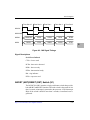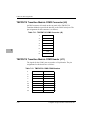
1
MCPN750A CompactPCI
Single Board Computer
Installation and Use
MCPN750A/IH5
September 2001 Edition
© Copyright 2001 Motorola, Inc.
All Rights Reserved.
Printed in the United States of America.
Motorola and the stylized M logo are registered trademarks of Motorola, Inc.
PowerPC is a registered trademark of International Business Machines and is used by
Motorola Inc. under license from IBM Corporation.
CompactPCI is a registered trademark of PCI Industrial Computer Manufacturers Group.
All other product or service names mentioned in this document are trademarks or registered
trademarks of their respective holders.
Safety Summary
The following general safety precautions must be observed during all phases of operation, service, and repair of this
equipment. Failure to comply with these precautions or with specific warnings elsewhere in this manual could result
in personal injury or damage to the equipment.
The safety precautions listed below represent warnings of certain dangers of which Motorola is aware. You, as the
user of the product, should follow these warnings and all other safety precautions necessary for the safe operation of
the equipment in your operating environment.
Ground the Instrument.
To minimize shock hazard, the equipment chassis and enclosure must be connected to an electrical ground. If the
equipment is supplied with a three-conductor AC power cable, the power cable must be plugged into an approved
three-contact electrical outlet, with the grounding wire (green/yellow) reliably connected to an electrical ground
(safety ground) at the power outlet. The power jack and mating plug of the power cable meet International
Electrotechnical Commission (IEC) safety standards and local electrical regulatory codes.
Do Not Operate in an Explosive Atmosphere.
Do not operate the equipment in any explosive atmosphere such as in the presence of flammable gases or fumes.
Operation of any electrical equipment in such an environment could result in an explosion and cause injury or damage.
Keep Away From Live Circuits Inside the Equipment.
Operating personnel must not remove equipment covers. Only Factory Authorized Service Personnel or other
qualified service personnel may remove equipment covers for internal subassembly or component replacement or any
internal adjustment. Service personnel should not replace components with power cable connected. Under certain
conditions, dangerous voltages may exist even with the power cable removed. To avoid injuries, such personnel
should always disconnect power and discharge circuits before touching components.
Use Caution When Exposing or Handling a CRT.
Breakage of a Cathode-Ray Tube (CRT) causes a high-velocity scattering of glass fragments (implosion). To prevent
CRT implosion, do not handle the CRT and avoid rough handling or jarring of the equipment. Handling of a CRT
should be done only by qualified service personnel using approved safety mask and gloves.
Do Not Substitute Parts or Modify Equipment.
Do not install substitute parts or perform any unauthorized modification of the equipment. Contact your local
Motorola representative for service and repair to ensure that all safety features are maintained.
Observe Warnings in Manual.
Warnings, such as the example below, precede potentially dangerous procedures throughout this manual. Instructions
contained in the warnings must be followed. You should also employ all other safety precautions which you deem
necessary for the operation of the equipment in your operating environment.
Warning
To prevent serious injury or death from dangerous voltages, use extreme
caution when handling, testing, and adjusting this equipment and its
components.
Flammability
All Motorola PWBs (printed wiring boards) are manufactured with a flammability rating
of 94V-0 by UL-recognized manufacturers.
EMI Caution
!
Caution
This equipment generates, uses and can radiate electromagnetic energy. It
may cause or be susceptible to electromagnetic interference (EMI) if not
installed and used with adequate EMI protection.
Lithium Battery Caution
This product contains a lithium battery to power the clock and calendar circuitry.
!
Caution
!
Attention
!
Vorsicht
Danger of explosion if battery is replaced incorrectly. Replace battery only
with the same or equivalent type recommended by the equipment
manufacturer. Dispose of used batteries according to the manufacturer’s
instructions.
Il y a danger d’explosion s’il y a remplacement incorrect de la batterie.
Remplacer uniquement avec une batterie du même type ou d’un type
équivalent recommandé par le constructeur. Mettre au rebut les batteries
usagées conformément aux instructions du fabricant.
Explosionsgefahr bei unsachgemäßem Austausch der Batterie. Ersatz nur
durch denselben oder einen vom Hersteller empfohlenen Typ. Entsorgung
gebrauchter Batterien nach Angaben des Herstellers.
CE Notice (European Community)
!
Warning
This is a Class A product. In a domestic environment, this product may
cause radio interference, in which case the user may be required to take
adequate measures.
Motorola Computer Group products with the CE marking comply with the EMC Directive
(89/336/EEC). Compliance with this directive implies conformity to the following
European Norms:
EN55022 “Limits and Methods of Measurement of Radio Interference Characteristics
of Information Technology Equipment”; this product tested to Equipment Class A
EN55024 “Information Technology Equipment-Immunity characteristics-Limits and
methods of measurement”
Board products are tested in a representative system to show compliance with the above
mentioned requirements. A proper installation in a CE-marked system will maintain the
required EMC/safety performance.
In accordance with European Community directives, a “Declaration of Conformity” has
been made and is available on request. Please contact your sales representative.
Notice
While reasonable efforts have been made to assure the accuracy of this document,
Motorola, Inc. assumes no liability resulting from any omissions in this document, or from
the use of the information obtained therein. Motorola reserves the right to revise this
document and to make changes from time to time in the content hereof without obligation
of Motorola to notify any person of such revision or changes.
Electronic versions of this material may be read online, downloaded for personal use, or
referenced in another document as a URL to the Motorola Computer Group website. The
text itself may not be published commercially in print or electronic form, edited, translated,
or otherwise altered without the permission of Motorola, Inc.
It is possible that this publication may contain reference to or information about Motorola
products (machines and programs), programming, or services that are not available in your
country. Such references or information must not be construed to mean that Motorola
intends to announce such Motorola products, programming, or services in your country.
Limited and Restricted Rights Legend
If the documentation contained herein is supplied, directly or indirectly, to the U.S.
Government, the following notice shall apply unless otherwise agreed to in writing by
Motorola, Inc.
Use, duplication, or disclosure by the Government is subject to restrictions as set forth in
subparagraph (b)(3) of the Rights in Technical Data clause at DFARS 252.227-7013 (Nov.
1995) and of the Rights in Noncommercial Computer Software and Documentation clause
at DFARS 252.227-7014 (Jun. 1995).
Motorola, Inc.
Computer Group
2900 South Diablo Way
Tempe, Arizona 85282
Contents
About This Manual
Summary of Changes ...............................................................................................xviii
Overview of Contents ..............................................................................................xviii
Comments and Suggestions .....................................................................................xviii
Conventions Used in This Manual.............................................................................xix
CHAPTER 1
Hardware Preparation and Installation
Introduction................................................................................................................1-1
Product Description ............................................................................................1-1
Block Diagram ....................................................................................................1-1
Getting Started ...........................................................................................................1-3
Overview of Start-up Procedure .........................................................................1-3
Equipment Required ...........................................................................................1-4
Unpacking Instructions .......................................................................................1-5
ESD Precautions .................................................................................................1-5
Preparation .................................................................................................................1-6
Hardware Configuration .....................................................................................1-6
MCPN750A Base Board Preparation .................................................................1-6
Flash Bank Selection (J7) ............................................................................1-7
Stand-Alone Operating Mode (J8) ..............................................................1-8
System Considerations......................................................................................1-10
TMCPN710 Transition Module Preparation ....................................................1-11
Serial Ports 1 and 2....................................................................................1-13
COM3 and COM4 Asynchronous Serial Ports..........................................1-15
TM-PIMC-0001 Transition Module Preparation..............................................1-16
COM 1 and COM 2 Asynchronous Serial Ports........................................1-18
COM3 and COM4 Asynchronous Serial Ports..........................................1-20
Hardware Installation...............................................................................................1-21
Installing PMC Modules on the MCPN750A SBC ..........................................1-21
Installing the MCPN750A Baseboard ..............................................................1-24
Installing a TMCPN710 or TM-PIMC-0001 Transition Module .....................1-26
Installing PIMs on the TM-PIMC-0001 Transition Module .....................1-26
Installing the Transition Module in the Chassis ........................................1-28
MCPN750A Module Power Requirements .............................................................1-31
vii
CHAPTER 2
Startup and Operation
Introduction ............................................................................................................... 2-1
Applying Power ......................................................................................................... 2-1
Memory Maps............................................................................................................ 2-3
Processor Memory Map ..................................................................................... 2-3
Default Processor Memory Map ................................................................. 2-3
PCI Local Bus Memory Map ............................................................................. 2-4
CompactPCI Memory Map ................................................................................ 2-5
Address Decoding with the 21554 .............................................................. 2-5
L2 Cache............................................................................................................. 2-6
System Clock Generator..................................................................................... 2-6
PPC Bus Arbitration ........................................................................................... 2-6
PCI Host Bridge ................................................................................................. 2-6
PCI Arbitration ................................................................................................... 2-8
Interrupt Handling .............................................................................................. 2-8
ISA DMA Channels ........................................................................................... 2-9
Sources of Reset ................................................................................................. 2-9
Power-On Reset ........................................................................................ 2-11
Undervoltage Reset ................................................................................... 2-11
Front Panel Push Button Reset.................................................................. 2-11
CompactPCI Reset (RST#) ....................................................................... 2-11
Watchdog Timer Reset.............................................................................. 2-11
Software Resets ......................................................................................... 2-12
Reset Source Identification ....................................................................... 2-12
Endian Issues .................................................................................................... 2-12
Processor/Memory Domain ...................................................................... 2-12
PCI Domain............................................................................................... 2-13
CHAPTER 3
PPCBug
PPCBug Overview..................................................................................................... 3-1
PPCBug Basics .......................................................................................................... 3-1
Memory Requirements ....................................................................................... 3-3
PPCBug Implementation .................................................................................... 3-3
MPU, Hardware, and Firmware Initialization ........................................................... 3-3
Using PPCBug ........................................................................................................... 3-5
Debugger Commands ......................................................................................... 3-6
Diagnostic Tests................................................................................................ 3-10
viii
CHAPTER 4
CNFG and ENV Commands
Overview....................................................................................................................4-1
CNFG - Configure Board Information Block ............................................................4-2
ENV - Set Environment .............................................................................................4-3
Configuring the PPCBug Parameters .................................................................4-3
CHAPTER 5
Remote Start Via the PCI Bus
Introduction................................................................................................................5-1
Overview.............................................................................................................5-1
Command/response Register Description...........................................................5-3
Opcode 0x01: Write/Read Virtual Register ........................................................5-5
Opcode 0x02: Initialize Memory ........................................................................5-5
Opcode 0x03: Write/Read Memory....................................................................5-6
Opcode 0x04: Checksum Memory .....................................................................5-6
Opcode 0x05: Memory Size Query ....................................................................5-7
Opcode 0x06: Debugger Query ..........................................................................5-7
Opcode 0x07: Execute Code...............................................................................5-7
Command/Response Channel Error Codes.........................................................5-8
Demonstration of the Host Interface...................................................................5-9
Reference Function: srom_crc.c .......................................................................5-12
CHAPTER 6
Functional Description
Introduction................................................................................................................6-1
Features ......................................................................................................................6-1
General Description ...................................................................................................6-2
Block Diagram ...........................................................................................................6-3
CompactPCI Bus Interface .................................................................................6-5
Ethernet Interface................................................................................................6-6
PCI Mezzanine Interface ....................................................................................6-7
ISA Bus Devices.................................................................................................6-8
Asynchronous Serial Ports...........................................................................6-8
Configuration and Status Registers .............................................................6-8
Serial EEPROM..................................................................................................6-8
PCI Peripheral Bus Controller (PBC) .................................................................6-9
ISA Interface................................................................................................6-9
EIDE Interface ...........................................................................................6-10
USB Interface ............................................................................................6-10
ISA Interrupt Controller ............................................................................6-10
ix
ISA DMA Channels .................................................................................. 6-10
Interval Timers .......................................................................................... 6-11
Real-Time Clock/NVRAM/Watchdog Timer Function ................................... 6-11
Replacing Lithium Batteries ..................................................................... 6-12
Hot Swap Control Circuitry ............................................................................. 6-14
Programmable Timers ...................................................................................... 6-14
Raven General Purpose Timers................................................................. 6-14
Raven Watchdog Timers........................................................................... 6-15
M48T559 Watchdog Timer....................................................................... 6-15
Interval Timers .......................................................................................... 6-16
Serial Port Signal Multiplexing ........................................................................ 6-16
I/O Signal Multiplexing (IOMX) .............................................................. 6-17
Signal Descriptions ................................................................................... 6-19
ABORT(ABT)/RESET (RST) Switch (S1)...................................................... 6-19
Front Panel Indicators (DS1 - DS3) ................................................................. 6-20
MPC750 Processor ........................................................................................... 6-20
Raven PCI-Host Bridge............................................................................. 6-20
Flash Memory ........................................................................................... 6-20
JTAG/COP ................................................................................................ 6-21
Bank A Flash Programming Enable.......................................................... 6-21
ECC Memory Controller .................................................................................. 6-22
DRAM Memory ............................................................................................... 6-22
Compact FLASH Memory Card ...................................................................... 6-22
TMCPN710 Transition Module ....................................................................... 6-23
TM-PIMC-0001................................................................................................ 6-23
CHAPTER 7
Connector Pin Assignments
MCPN750A and Transition Module Connectors ...................................................... 7-1
MCPN750A Connector Pin Assignments ................................................................. 7-2
MCPN750A CompactPCI Bus Connectors (J1/J2)............................................ 7-2
MCPN750A CompactPCI User I/O Connector J3 ............................................. 7-4
MCPN750A Connector J4.................................................................................. 7-6
MCPN750A CompactPCI User I/O Connector (J5) .......................................... 7-7
MCPN750A PCI Mezzanine Card Connectors
(J11/21, J12/22, J13/23, J14/24 .......................................................................... 7-9
MCPN750A 10BaseT/100BaseTx Connector (J18) ........................................ 7-12
MCPN750A Debug Connector (J19) ............................................................... 7-12
MCPN750A Processor RISCWatch Debug Connector (J6)............................. 7-17
TMCPN710 Transition Module............................................................................... 7-18
TMCPN710 Transition Module CompactPCI Connectors (J3/J4/J5) .............. 7-18
x
TMCPN710 Transition Module COM1 Connector (J6) ...................................7-19
TMCPN710 Transition Module COM2 Connector (J8) ...................................7-20
TMCPN710 Transition Module COM3 Header (J11) ......................................7-20
TMCPN710 Transition Module COM4 Header (J14) ......................................7-21
TMCPN710 Transition Module 10BaseT/100BaseTx Connector (J13) ..........7-22
TMCPN710 Transition Module USB Connectors (J10, J12) ...........................7-23
TMCPN710 Transition Module IDE Compact FLASH Connectors
(J15, J16)...........................................................................................................7-23
TMCPN710 Transition Module PMC I/O Connectors (J1/J2) .........................7-25
TM-PIMC-0001 Transition Module ........................................................................7-27
TM-PIMC-0001 CompactPCI User I/O Connector (J3, J4, & J5) ...................7-27
TM-PIMC-0001 Transition Module COM1 Connector (J9) ............................7-28
TM-PIMC-0001 Transition Module COM2 Connector (J8) ............................7-29
TM-PIMC-0001 Transition Module COM3 and COM4 Connectors
(J12 & J13)........................................................................................................7-30
TM-PIMC-0001 Transition Module 10BaseT/100BaseTx Connector (J7)......7-31
TM-PIMC-0001 Transition Module IDE Compact FLASH Connector (J1)....7-31
TM-PIMC-0001 Transition Module PMC I/O Connectors
(J10, J20, and J14/J24)......................................................................................7-33
APPENDIX A
Specifications
Specifications ............................................................................................................A-1
Cooling Requirements ..............................................................................................A-2
EMC Compliance......................................................................................................A-3
APPENDIX B
Related Documentation
Motorola Computer Group Documents .................................................................... B-1
Manufacturers’ Documents....................................................................................... B-2
Related Specifications............................................................................................... B-4
xi
xii
List of Figures
Figure 1-1. MCPN750A Base Board Block Diagram................................................1-2
Figure 1-2. MCPN750A Switches, Headers, Connectors, Fuses, LEDs ...................1-9
Figure 1-3. TMCPN710 Connector and Header Locations .....................................1-12
Figure 1-4. MCPN750A/TMCPN710 Serial Ports 1 and 2 .....................................1-14
Figure 1-5. TMCPN710 Serial Ports 3 and 4...........................................................1-15
Figure 1-6. TM-PIMC-0001 Connector and Header Locations...............................1-17
Figure 1-7. MCPN750A/TM-PIMC-0001 Serial Ports 1 and 2...............................1-19
Figure 1-8. TM-PIMC-0001 Serial Ports 3 and 4 ....................................................1-20
Figure 1-9. PMC Module Placement on MCPN750A .............................................1-22
Figure 1-10. TMCPN710 or TM-PIMC-0001/MCPN750A Mating Configuration 1-30
Figure 2-1. PPCBug System Startup..........................................................................2-2
Figure 6-1. MCPN750A Block Diagram ...................................................................6-4
Figure 6-2. Serial Port Signal Multiplexing.............................................................6-17
Figure 6-3. MX Signal Timings ...............................................................................6-19
xiii
xiv
List of Tables
Table 1-1. Startup Overview ......................................................................................1-3
Table 1-2. Installing a PIM on the TM-PIMC-0001 Transition Module .................1-27
Table 2-1. Processor Default View of the Memory Map ...........................................2-3
Table 2-2. Classes of Reset and Effectiveness .........................................................2-10
Table 3-1. Debugger Commands ...............................................................................3-7
Table 3-2. Diagnostic Test Groups...........................................................................3-11
Table 5-1. Command/Respond Error Codes ..............................................................5-8
Table 6-1. MCPN750A Features................................................................................6-1
Table 6-2. Multiplexing Sequence of the MX Function ..........................................6-18
Table 7-1. MCPN750A J1 CompactPCI Connector ..................................................7-2
Table 7-2. MCPN750A J2 CompactPCI Connector ..................................................7-3
Table 7-3. MCPN750A J3 User I/O Connector .........................................................7-5
Table 7-4. MCPN750A J5 User I/O Connector .........................................................7-7
Table 7-5. MCPN750A PCI Mezzanine Card Connector ..........................................7-9
Table 7-6. MCPN750A PCI Mezzanine Card Connector ........................................7-10
Table 7-7. MCPN750A 10BaseT/100BaseTx Connector J18 .................................7-12
Table 7-8. MCPN750A Debug Connector (J19)......................................................7-13
Table 7-9. MCPN750A RISCWatch Debug Connector (J6)....................................7-17
Table 7-10. TMCPN710 COM1 Connector (J6)......................................................7-19
Table 7-11. TMCPN710 COM2 Connector (J8)......................................................7-20
Table 7-12. TMCPN710 COM3/COM4 Headers ....................................................7-20
Table 7-13. TMCPN710 10BaseT/100BaseTx Connector (J13) .............................7-22
Table 7-14. TMCPN710 USB 0 Connector (J10) ....................................................7-23
Table 7-15. TMCPN710 USB 1 Connector (J12) ....................................................7-23
Table 7-16. TMCPN710 Compact FLASH IDE Connectors...................................7-24
Table 7-17. TMCPN710 PMC 1 and 2 I/O Connector ............................................7-25
Table 7-18. TM-PIMC-0001 COM1 Connector (J9) ...............................................7-28
Table 7-19. TM-PIMC-0001 COM2 Connector (J8) ...............................................7-29
Table 7-20. TM-PIMC-0001 COM3 and COM4 Headers .......................................7-30
Table 7-21. TM-PIMC-0001 10BaseT/100BaseTx Connector (J7).........................7-31
Table 7-22. TM-PIMC-0001 CompactFLASH IDE Connector (J1) .......................7-32
Table 7-23. TM-PIMC-0001 PMC I/O Module 1 (PIM1) - Host I/O
Connector Pin Assignments .....................................................................................7-33
Table 7-24. TM-PIMC-0001 PMC I/O Module 2 (PIM2) - Host I/O
Connector Pin Assignments .....................................................................................7-34
xv
Table 7-25. PMC I/O Modules 1 and 2 (PIM1 and PIM2) PMC I/O Connector Pin Assignments..................................................................... 7-36
Table A-1. MCPN750 Specifications ...................................................................... A-1
Table B-1. Motorola Computer Group Documents ................................................. B-1
Table B-2. Manufacturers’ Documents ................................................................... B-2
Table B-3. Related Specifications ........................................................................... B-4
xvi
About This Manual
This manual, MCPN750A CompactPCI Single Board Computer
Installation and Use (MCPN750A/IH5) provides general information,
hardware preparation and installation instructions, operating instructions,
firmware information, functional descriptions, and pin assignments for the
MCPN750A family of Single Board Computers. In addition, sufficient
information is also provided for the two transition modules manufactured
by Motorola for use with the MCPN750A (TMCPN710 and TM-PIMC0001). The document should be used by anyone who wants general, as well
as technical information about the MCPN750A products.
Note: This revision of the MCPN750A Installation and Use manual
supersedes all previous versions of this document.
Currently, the boards are provided in the following configurations:
Part Number
Description
MCPN750-1222A
MPC750, 266MHz, 16MB ECC DRAM, 5MB FLASH, 1MB L2 Cache
MCPN750-1232A
MPC750, 266MHz, 32MB ECC DRAM, 5MB FLASH, 1MB L2 Cache
MCPN750-1332A
MPC750, 366MHz, 32MB ECC DRAM, 5MB FLASH, 1MB L2 Cache
MCPN750-1342A/B
MPC750, 366MHz, 64MB ECC DRAM, 5MB FLASH, 1MB L2 Cache
MCPN750-1352A/B
MPC750, 366MHz, 128MB ECC DRAM, 5MB FLASH, 1MB L2 Cache
MCPN750-1362A
MPC750, 366MHz, 256MB ECC DRAM, 5MB FLASH, 1MB L2 Cache
MCPN750-1442A
MCP750, 466MHz, 64MB ECC DRAM, 5MB FLASH, 1MB L2 Cache
MCPN750-2342A/B
MPC750, 366MHz, 64MB ECC DRAM, 5MB FLASH, 1MB L2 Cache,
Transition Module, Ethernet Rear I/O
MCPN750-2352A/B
MPC750, 366MHz, 128MB ECC DRAM, 5MB FLASH, 1MB L2 Cache,
Transition Module, Ethernet Rear I/O
MCPN750-2352A-F
MPC750, 366MHz, 128MB ECC DRAM, 5MB FLASH, 1MB L2 Cache,
Transition Module, Ethernet Rear I/O
MCPN750-2362A/B
MPC750, 366MHz, 256MB ECC DRAM, 5MB FLASH, 1MB L2 Cache,
Transition Module, Ethernet Rear I/O
xvii
Summary of Changes
The following is a list of changes made since the last release of this
manual.
Date
Changes
Replaces
09/01
Updated table of model numbers
preceeding this section.
Reinserted information left out of IH4
version of manual, which included
information on MCPN750A, the
TMCPN710 and the TM-PIMC-0001,
instead of the earlier MCPN750. Also,
included J8 jumper settings for StandAlone operation.
Previously listed model numbers.
07/00
68-pin .08 Series Subminature D PMC I/O
Connector.
68-pin .050 Series Subminature
D PMC I/O Connector.
Overview of Contents
This section provides a brief overview of each chapter and appendix within
this document.
Chapter 1, Hardware Preparation and Installation, provides a brief
product description and a block diagram. The remainder of the chapter
provides information on hardware preparation and installation
instructions, including peripheral boards such as the TMCPN710 or TMPIMC-0001 Transition Module.
Chapter 2, Startup and Operation, provides an overview of basic operating
and configuring issues such as the PPCBug firmware, the memory maps,
interrupts, arbitration, sources of reset and endian issues.
Chapter 3, PPCBug, provides an overview and description of basic
PPCBug use including implementation issues, a list of the initialization
sequence, a description of basic debugger commands, as well as a list of
diagnostic tests typically run.
xviii
Chapter 4, CNFG and ENV Commands, provides an explanation of two of
the more important PPCBug configuration commands: CNFG and ENV.
Includes information on how to configure the VMEbus and PCI bus
environments using the ENV command.
Chapter 5, Remote Start Via the PCI Bus, provides a description of the
remote start capability that is available via the PCI bus using PPCBug
commands.
Chapter 6, Functional Description, provides a description of the major
components and functionality of the MCPN750A.
Chapter 7, Connector Pin Assignments, provides a listing of all major
connector pinout information for the MCPN750A, the TMCPN710, and
TM-PIMC-0001.
Appendix A, Specifications, provides basic board specification
information including recommendations on cooling and EMC compliance.
Appendix B, Related Documentation, provides a listing of related
motorola and vendor documentation, as well as a list of related industry
standard specifications.
Comments and Suggestions
Motorola welcomes and appreciates your comments on its documentation.
We want to know what you think about our manuals and how we can make
them better. Mail comments to:
Motorola Computer Group
Reader Comments DW164
2900 S. Diablo Way
Tempe, Arizona 85282
You can also submit comments to the following e-mail address:
[email protected]
xix
In all your correspondence, please list your name, position, and company.
Be sure to include the title and part number of the manual and tell how you
used it. Then tell us your feelings about its strengths and weaknesses and
any recommendations for improvements.
Conventions Used in This Manual
The following typographical conventions are used in this document:
bold
is used for user input that you type just as it appears; it is also used for
commands, options and arguments to commands, and names of
programs, directories and files.
italic
is used for names of variables to which you assign values. Italic is also
used for comments in screen displays and examples, and to introduce
new terms.
courier
is used for system output (for example, screen displays, reports),
examples, and system prompts.
<Enter>, <Return> or <CR>
<CR> represents the carriage return or Enter key.
CTRL
represents the Control key. Execute control characters by pressing the
Ctrl key and the letter simultaneously, for example, Ctrl-d.
xx
1Hardware Preparation and
Installation
1
Introduction
This chapter provides startup and safety instructions related to this
product, hardware preparation instructions - including default jumper
settings, system considerations, and installation instructions for the
baseboard, as well as the PMCs and transition modules associated with this
board.
A fully implemented MCPN750A consists of the baseboard plus:
❏
One or two optional PCI mezzanine cards (PMC) for additional
versatility
❏
One of two different types of optional transition modules: the
TMCPN710 or the TM-PIMC-0001 for added I/O flexibility
Product Description
The MCPN750A is a hot swappable CompactPCI, non-system slot, single
board computer based on the PowerPlus architecture. It consists of the
MPC750 processor with L2 cache, the Raven PCI Bridge and Interrupt
Controller, the ECC Memory Controller Falcon chipset, 5MB of linear
Flash memory, 16MB to 256MB of ECC protected DRAM, interface to a
CompactPCI bus, and several I/O peripherals.
Block Diagram
The block diagram in Figure 1-1 illustrates the architecture of the
MCPN750A baseboard.
1-1
Hardware Preparation and Installation
DRAM
(Bank 1)
16M/64M/128M
Arbitration
Control
L2 Cache
1M
Processor
MPC750
66MHz PPC603 Processor Bus
Debug Connector
DRAM
(Bank 2)
16M/64M/128M
Flash
(soldered)
4M
Memory
Controller
Falcon 3
Chipset
Flash
(socketed)
1M
SROM
AT24C04
PCI Bridge
& MPIC
Raven 5 ASIC
System
Registers
Interrupt
Serializer
Core Power
32/64-bit PMC Slot 1
Clock
Generator
Reset
Control
Hot Swap
Control
33MHz 32/64-bit PCI Local Bus
RS232
IOMX
User I/O J3 & J5
SERIAL 1
SERIAL 2
SERIAL 3
SERIAL 4
(OPTIONAL ROUTING TO TM)
PMC Slot 1
PMC Slot 2
UARTs
16C550C
33MHz 32/64-bit CompactPCI Bus
NVRAM/
WD/RTC
MK48T559
EIDE
ISA
Registers
PCI-PCI BRIDGE
Intel 21554
USB1
PBC
VT82C586B
ISA
10BT/
100BTx
Serial
Ethernet
Ethernet
Intel 21143
USB0
32/64-bit PMC Slot 2
1
CompactPCI J1/J2
Figure 1-1. MCPN750A Baseboard Block Diagram
1-2
Computer Group Literature Center Web Site
Getting Started
Getting Started
This section provides an overview of the steps necessary to install and
power up the MCPN750A, any additional equipment requirements, and a
brief section on unpacking and ESD precautions. As identified in the table
below, several steps can be omitted if your board, for example, has been
shipped with PMCs and Flash already installed
Overview of Start-up Procedure
The following table lists the things you will need to do before you can use
this board and tells where to find the information you need to perform each
step. Be sure to read this entire chapter, including all Caution and Warning
notes, before you begin.
Table 1-1. Startup Overview
Task
Section or Manual Reference
Page
Unpack the hardware.
Unpacking Instructions
Configure the hardware by
setting jumpers on the baseboard
and transition module.
MCPN750A Baseboard Preparation and
TMCPN710 or TM-PIMC-0001 Transition Module
Preparation
1-5
Ensure CompactFlash card is
installed (if required)
Compact Flash Memory Card Installation
1-6
Install the PMC Module (if
required)
PMC Module Installation
1-21
Install the MCPN750A in the
chassis.
MCPN750A CompactPCI SBC Installation
1-24
Install the transition module in
the chassis.
TMCPN710 or TM-PIMC-0001 Transition Module
Installation
1-26
Connect any other equipment
you will be using.
Connector Pin Assignments
7-1
Power up the system.
Applying Power
1-6, 1-11,
and 1-16
For more information on optional devices and
equipment, refer to the documentation provided with
the equipment.
http://www.motorola.com/computer/literature
2-1
1-3
1
1
Hardware Preparation and Installation
Table 1-1. Startup Overview (Continued)
Task
Section or Manual Reference
Page
Note that the debugger initializes
the MCPN750A
Using PPCBug
3-5
You may also wish to obtain the PPCBug Firmware
Package User’s Manual, listed in Appendix B,
Related Documentation.
B-1
Initialize the system clock.
Using the Debugger, Debugger Commands, the
SET command
3-6
Examine and/or change
environmental parameters.
CNFG and ENV Commands
Program the board as needed for
your applications.
MCPN750A CompactPCI Single Board Computer
Programmer’s Reference Guide, listed in Appendix
B, Related Documentation.
4-2
and 4-3
B-1
Equipment Required
The following equipment is required to complete an MCPN750A system:
❏
CompactPCI system enclosure
❏
System console terminal
❏
Operating system (and/or application software)
❏
Disk drives (and/or other I/O) and controllers
❏
Transition module (TMCPN710 or TM-PIMC-0001) and
connecting cables
MCPN750A baseboards are factory-configured for I/O handling via a
TMCPN710 or TM-PIMC-0001 transition module. There are currently
eight MCPN750A models corresponding to the five separate memory
configurations, two processor speeds and front or rear ethernet I/O. Either
one of the aforementioned transition modules support all models of the
baseboard. Refer to the subsections on the MCPN750A and transition
module installation for more information.
1-4
Computer Group Literature Center Web Site
Getting Started
Unpacking Instructions
Note
If the shipping carton is damaged upon receipt, request that
the carrier’s agent be present during the unpacking and
inspection of the equipment.
Unpack the equipment from the shipping carton. Refer to the packing list
and verify that all items are present. Save the packing material for storing
and reshipping of equipment.
Avoid touching areas of integrated circuitry; static discharge can damage
circuits.
!
Caution
ESD Precautions
Motorola strongly recommends that you use an antistatic wrist strap and a
conductive foam pad when installing or upgrading a system. Electronic
components, such as disk drives, computer boards, and memory modules, can
be extremely sensitive to ESD. After removing the component from the system
or its protective wrapper, place the component flat on a grounded, static-free
surface (and in the case of a board, component side up). Do not slide the
component over any surface.
If an ESD station is not available, you can avoid damage resulting from ESD
by wearing an antistatic wrist strap (available at electronics stores) that is
attached to an unpainted metal part of the system chassis.
!
Inserting or removing modules with power applied may result in damage
to module components.
Caution
!
Warning
Dangerous voltages, capable of causing death, are present in
this equipment. Use extreme caution when handling, testing,
and adjusting.
http://www.motorola.com/computer/literature
1-5
1
1
Hardware Preparation and Installation
Preparation
This section discusses certain hardware and software tasks that may need
to be performed prior to installing the board in a CompactPCI chassis.
Hardware Configuration
To produce the desired configuration and ensure proper operation of the
MCPN750A, you may need to carry out certain hardware modifications
before installing the module.
The MCPN750A provides software control over most options by setting
bits in control registers after installing the module in a system. You can
also modify the board’s configuration by modifying similar control
registers. The MCPN750A control registers are described in the
MCPN750A CompactPCI Single Board Computer Programmer’s
Reference Guide (MCPN750A/PG), which can be accessed on line in pdf
or html format through the Motorola Computer Group Literature web site
(http://www.motorola.com/computer/literature).
Some options, however, are not software-programmable. These options
are controlled by installing or removing header jumpers or interface
modules on the baseboard or the associated transition module.
MCPN750A Baseboard Preparation
Figure 1-2 illustrates the placement of the switches, jumper headers,
connectors, and LED indicators on the MCPN750A. Manually configured
items on the baseboard include:
❏
Flash bank selection (J7)
❏
Stand-Alone Operating Mode (J8)
For a discussion of the configured items on the transition module, refer in
this chapter to the sections titled TMCPN710 Transition Module
Preparation, or to the respective user’s manuals for the transition modules
(listed in the Related Documentation appendix) as necessary.
1-6
Computer Group Literature Center Web Site
Preparation
The MCPN750A is factory tested and shipped with the configurations
described in the following sections. The MCPN750A’s required and
factory-installed debug monitor, PPCBug, operates with those factory
settings.
Flash Bank Selection (J7)
The MCPN750A baseboard has provision for 1MB of 16-bit Flash
memory and 4MB of linear Flash memory.
The Flash memory is organized in two banks, Bank A is 64 bits wide and
Bank B is 16 bits wide. Bank B contains the onboard debugger, PPCBug.
To enable Flash Bank A, place a jumper across header J7 pins 1 and 2. To
enable Flash Bank B (1MB of firmware located in sockets on the
baseboard), place a jumper across header J7 pins 2 and 3.
J7
3
3
2
2
1
1
Flash Bank A Enabled (4MB Soldered)
Note
J7
Flash Bank B Enabled (1MB, Sockets)
(Factory Configuration)
Placing a jumper on Flash programming header J9 has no affect.
The Flash programming for Bank A is permanently enabled with
onboard resistors.
http://www.motorola.com/computer/literature
1-7
1
1
Hardware Preparation and Installation
Stand-Alone Operating Mode (J8)
The MCPN750A has a stand-alone operating mode that allows the
MCPN750A to function without the clock from the system slot controller
board. Installing a jumper across pins 1 and 2 of J8 enables the stand-alone
mode. The J8 jumper must be removed for normal operation.
J8
2
2
1
1
Enables Stand-Alone mode
Note
1-8
J8
Remove jumper for normal operation
(Factory Configuration)
An MCPN750A configured for stand-alone mode should not be
installed in a chassis with a system slot controller board. This will
result in unpredictable system operation. See the section on
System Considerations for additional information.
Computer Group Literature Center Web Site
3
1
3
1
1
2
1
1
J9 2
J7
J8
J6
15
1
J5
U1
U2
2
1
J24
64
63
2
1
2
1
J11
J12
64
63
64
63
2
1
2
1
J13
J14
64
63
64
63
J3
64
63
64
63
J4
J22
J23
U12
U13
U14
U15
U16
2
1
U6
U7
U8
U9
64
63
U5
XU2
U20
U23
J21
XU1
PCI MEZZANINE CARD 1
J2
L2
U35
J18
10/100 BASE T
DS1
DS2
U31
S1
J1
J19
Q3
COM 1
DS3
Q4
2703 0002
1-9
http://www.motorola.com/computer/literature
2
16
2
PCI MEZZANINE CARD 2
BFL CPU
ABT/RST
Figure 1-2. MCPN750A Switches, Headers, Connectors, Fuses, LEDs
1
Preparation
1
Hardware Preparation and Installation
System Considerations
The MCPN750A is designed to operate as a CompactPCI non-system slot
board. Consequently, the MCPN750A must be installed in the subrack
system slot marked with the circle symbol.
The MCPN750A can operate properly, with or without a system slot
controller board. In the standard operating mode (with a system slot
board), the system slot board is used to provide clock and arbitration
signals to the MCPN750A. In the stand-alone mode, a jumper must be set
on the MCPN750A, in order to obtain clock signals from other on-board
devices.
Installing a jumper on J8 routes an onboard PCI clock to the 21554 primary
side clock input. This allows the MCPN750A to operate in a chassis
without a system slot controller board installed. The chassis must provide
+5V, +3.3V, +12V, -12V and VIO to the MCPN750A, and the BD_SEL
pin (P1-D15) in the chassis must be grounded. In addition, in the standalone mode, the MCPN750A cannot communicate over the CompactPCI
backplane.
On the MCPN750A baseboard, the standard serial console port (COM1)
serves as the PPCBug debugger console port. The firmware console should
be set up as follows:
❏
Eight bits per character
❏
One stop bit per character
❏
Parity disabled (no parity)
❏
Baud rate of 9600 baud
9600 baud is the power-up default for serial ports on MCPN750A boards.
After power-up you can reconfigure the baud rate if you wish, using the
PPCBug PF (Port Format) command via the command line interface.
Whatever the baud rate, some type of hardware handshaking — either
XON/OFF or via the RTS/CTS line — is desirable if the system supports
it.
1-10
Computer Group Literature Center Web Site
Preparation
TMCPN710 Transition Module Preparation
The TMCPN710 transition module (Figure 1-3) is used in conjunction
with all models of the MCPN750A baseboard:
The features of the TMCPN710 include:
❏
Two EIA-232-D asynchronous serial ports (identified as COM1 and
on the transition module panel)
COM2
❏
Two USB Series A connectors for USB interface
❏
One 10/100BaseT connector for ethernet connections (requires
MCPN750A Transition module/ethernet option)
❏
Two 68-pin .08 Series Subminiature D connectors for PMC I/O
❏
Two 50-pin on-board connectors for EIDE interface to one or two
Compact Flash plug-in modules
http://www.motorola.com/computer/literature
1-11
1
7
J13
1
2
7
1
J8
7
1
2
J6
J7
(Slave)
J16
PMC2 I/O
J2
J3
3
COM 1
8
1
2
J11
COM 2
J4
8
1
J10
USB 0
4
1
J12
USB 1
4
J14
J5
10/100 BASE T
8
2286 9806
Hardware Preparation and Installation
J1
J15
PMC1 I/O
(Master)
1
Figure 1-3. TMCPN710 Connector and Header Locations
1-12
Computer Group Literature Center Web Site
Preparation
Serial Ports 1 and 2
On the TMCPN710, the asynchronous serial ports (Serial Ports 1 and 2)
are configured permanently as data circuit-terminating (Figure 1-4)
equipment (DTE). The COM1 port is also routed to a RJ-45 connector on
the front panel of the processor board. A terminal for COM1 may be
connected to either the processor board or the transition module, but not
both.
Jumper J7 on the transition module must be configured to enable COM1
on either the transition module or the processor board. To enable the
COM1 port on the transition module, connect pins 2-3 of J7. To enable
COM1 on the processor board, connect pins 1-2 of J7.
J7
J7
Serial Port 1 jumper settings
1
2
3
Enable COM1 on TMCPN710
Note
1
2
3
Enable COM1 on MCPN750A (factory configuration)
If the J7 jumper is not present on the TMCPN710, the board
automatically enables COM1 on the MCPN750A.
http://www.motorola.com/computer/literature
1-13
1
1
Hardware Preparation and Installation
MCPN750A
RJ45
1
8
7
COM1
(front panel)
2
5
TMCPN710
4
3
J7
6
COM1
(rear panel)
16C550
SOUT
4
SIN
5
RTS
2
CTS
7
DTR
8
DCD
1
J3
DSR
3
6
RI
IO
MUX
IO
MUX
16C550
RI
DSR
COM2
(rear panel)
DCD
1
DTR
8
CTS
7
RTS
2
SIN
5
SOUT
4
3
6
2362 9808
Figure 1-4. MCPN750A/TMCPN710 Serial Ports 1 and 2
1-14
Computer Group Literature Center Web Site
Preparation
COM3 and COM4 Asynchronous Serial Ports
The signals for COM3 and COM4 serial ports are routed to headers on the
TMCPN710 Transition Module. These headers are intended for debug
purposes only. Figure 1-5 depicts this configuration.
TMCPN710
MCPN750A
J11
16C550
SOUT
3
SIN
5
RTS
7
CTS
9
DTR
14
DCD
15
J3
DSR
Com3
Header
11
18
RI
IO
MUX
IO
MUX
16C550
13
J14
RI
18
DSR
11
DCD
15
DTR
14
CTS
9
RTS
7
SIN
5
Com4
Header
3
SOUT
13
2363 9808
Figure 1-5. TMCPN710 Serial Ports 3 and 4
http://www.motorola.com/computer/literature
1-15
1
1
Hardware Preparation and Installation
TM-PIMC-0001 Transition Module Preparation
The TM-PIMC-0001 transition module (Figure 1-6) is used in conjunction
with all models of the MCPN750A baseboard. The features of this
transition module include:
1-16
❏
Connections for two single wide, or one double wide PIM card.
❏
Two asynchronous serial ports using RJ-45 connectors labeled as
COM1 and COM2.
❏
Two asynchronous serial ports using 10-pin headers labeled as
COM3 and COM4.
❏
One ethernet port using an RJ-45 connector
❏
One IDE Flash connector using a standard 50-pin CompactFlash
socket.
Computer Group Literature Center Web Site
http://www.motorola.com/computer/literature
1
2
7
8
COM 1
J9
J2
1
3
J8
7
8
J11
COM 2
1
2
1
3
J1
1
2
J7
J12
7
8
1
9
1
64
63
10/100 BASE T
2
2
J13
9
J14
PMC I/O MODULE 1
2 64
1 63
J3
J10
2 64
1 63
J4
J24
PMC I/O MODULE 2
2 64
1 63
J20
J5
2
1
8
1
J16
2694 0001
Preparation
Figure 1-6. TM-PIMC-0001 Connector and Header Locations
1-17
1
1
Hardware Preparation and Installation
COM1 and COM2 Asynchronous Serial Ports
On the TM-PIMC-0001, the asynchronous serial ports (COM1 and
COM2) are configured permanently as data circuit-terminating
(Figure 1-7) equipment (DTE). The COM1 port is also routed to an RJ45
connector on the front panel of the processor board. A terminal for COM1
may be connected to either the processor board or the transition module,
but not both.
Jumper J11 on the transition module must be configured to enable COM1
on the processor board. If J11 is not configured, COM1 is automatically
routed to PIM 1 on the transition module. Jumper J2 on the transition
module must be configured in the same way for the COM2 port.
J11
J11
Serial Port 1 jumper settings
1
2
3
Enable COM1 for PIM1
of TM-PIMC-0001
1
2
3
Enable COM1 on MCPN750A
J2
J2
Serial Port 2 jumper settings
1
2
3
Enable COM2 for PIM2
of TM-PIMC-0001
1-18
1
2
3
Enable COM2 on MCPN750A
Computer Group Literature Center Web Site
Preparation
TM-PIMC-0001
MCPN750
RJ45
1
8
7
COM1
(front panel)
PIM 1
2
5
4
3
J11
6
COM1
(rear panel)
16C550
4
SOUT
5
SIN
IO
MUX
RTS
2
CTS
7
DTR
8
1
DCD
J3
DSR
3
6
RI
IO
MUX
IO
MUX
16C550
RI
DSR
COM2
(rear panel)
DCD
1
8
DTR
IO
MUX
CTS
7
RTS
2
SIN
5
SOUT
4
3
J2
6
PIM 2
2362 0001
Figure 1-7. MCPN750A/TM-PIMC-0001 Serial Ports 1 and 2
http://www.motorola.com/computer/literature
1-19
1
1
Hardware Preparation and Installation
COM3 and COM4 Asynchronous Serial Ports
The signals for COM3 and COM4 serial ports are routed to 10-pin headers
on the TM-PIMC-0001 Transition Module (J12 and J13). These headers
function as I/O connectors for the MCPN750A and are permanently
configured as DTE. Figure 1-8 depicts this configuration.
TM-PIMC-0001
MCPN750A
J12
16C550
SOUT
5
SIN
3
RTS
4
CTS
6
DTR
7
DCD
1
J3
DSR
Com3
Header
2
8
RI
IO
MUX
IO
MUX
16C550
9
J13
RI
8
DSR
2
DCD
1
DTR
7
CTS
6
RTS
4
SIN
3
SOUT
5
Com4
Header
9
2363 0001
Figure 1-8. TM-PIMC-0001 Serial Ports 3 and 4
1-20
Computer Group Literature Center Web Site
Hardware Installation
Hardware Installation
The following sections discuss the placement of PMC mezzanine cards on
the MCPN750A baseboard and the installation of the complete
MCPN750A assembly into a CompactPCI chassis. Before installing the
MCPN750A, ensure that all header jumpers are configured as desired.
In most cases, PMC modules ordered with the baseboard are installed on
the MCPN750A at the factory and the order is shipped as a single unit. The
user-configured jumpers on the PMCs are accessible with the mezzanines
installed.
If it is necessary to install mezzanines on the baseboard, refer to the
following sections for a brief description of the installation procedure.
Note: the procedure assumes the MCPN750A has already been installed in
the chassis. If not, begin with Step 4.
!
Avoid touching areas of integrated circuitry; static discharge can damage
these circuits.
Caution
Installing PMC Modules on the MCPN750A SBC
One dual wide, one single wide or two single wide PCI mezzanine (PMC)
modules can be mounted on top of the MCPN750A baseboard. The
MCPN750A is designed to accept only +5V or Universal PMCs. Due to
pin current limitations, the MCPN750A can supply up to 4.5 amps to a
single PMC on each of the +3.3V and +5V supplies. The MCPN750A can
supply a maximum of 500mA at +12V and -12V to each PMC. Refer to the
table on page 1-31 for the total current available to PMC’s and transition
modules. To install a PMC module, refer to Figure 1-9 PMC Carrier Board
Placement on MCPN750A, and proceed as follows:
1. Attach an ESD strap to your wrist. Attach the other end of the ESD
strap to the chassis as a ground. The ESD strap must be secured to
your wrist and to ground throughout the procedure.
2. Perform an operating system shutdown. Turn the AC or DC power
off and remove the AC cord or DC power lines from the system.
http://www.motorola.com/computer/literature
1-21
1
1
Hardware Preparation and Installation
3. Remove chassis or system cover(s) as necessary for access to the
CompactPCI.
2288 9806
Figure 1-9. PMC Module Placement on MCPN750A
!
Caution
!
Warning
Inserting or removing modules in a non-hot swap chassis with power
applied may result in damage to module components. The MCPN750A is
a hot swappable board and may be inserted in a hot swap chassis, such as
a CPX2000 or a CPX8000 series chassis with power applied.
Dangerous voltages, capable of causing death, are present in
this equipment. Use extreme caution when handling, testing,
and adjusting.
4. Carefully remove the MCPN750A from its CompactPCI card slot
and lay it flat, with connectors J1 through J5 facing you.
1-22
Computer Group Literature Center Web Site
Hardware Installation
!
Caution
Avoid touching areas of integrated circuitry; static discharge can damage
these circuits.
5. Remove the PMC filler from the front panel of the MCPN750A.
6. Slide the edge connector of the PMC module into the front panel
opening from behind and place the PMC module on top of the
baseboard. The four connectors on the underside of the PMC
module should then connect smoothly with the corresponding
connectors (J11/12/13/14) on the MCPN750A.
7. Insert the four short Phillips screws, provided with the PMC,
through the holes on the bottom side of the MCPN750A into the
PMC front bezel and rear standoffs. Tighten the screws.
8. Reinstall the MCPN750A assembly in its proper card slot. Be sure
the module is well seated in the backplane connectors. Do not
damage or bend connector pins.
9. Replace the chassis or system cover(s), reconnect the system to the
AC or DC power source, and turn the equipment power on.
Note
If the PMC provides rear I/O, refer to Chapter 7, Connector Pin
Assignments for the pin assignments. Connectors on the
TMCPN710 and TM-PIMC-0001 provide rear panel access to
these signals.
http://www.motorola.com/computer/literature
1-23
1
1
Hardware Preparation and Installation
Installing the MCPN750A Baseboard
With mezzanine board(s) installed (if applicable) and headers properly
configured, proceed as follows to install the MCPN750A in the
CompactPCI chassis:
1. Attach an ESD strap to your wrist. Attach the other end of the ESD
strap to the chassis as a ground. The ESD strap must be secured to
your wrist and to ground throughout the procedure.
2. In a non-hot swap system, perform an operating system shutdown.
Turn the AC or DC power off and remove the AC cord or DC power
lines from the system. Remove chassis or system cover(s) as
necessary for access to the CompactPCI modules.
!
Caution
Inserting or removing modules in a non-hot swap chassis with power
applied may result in damage to module components. The MCPN750A is
a hot swappable board and may be inserted in a hot swap chassis such as a
CPX2000, or a CPX8000 series chassis with power applied.
Dangerous voltages, capable of causing death, are present in
this equipment. Use extreme caution when handling, testing,
and adjusting.
3. Remove the filler panel from the appropriate non-system card slot.
4. Set the VIO on the backplane to either +3.3V or +5V (the
MCPN750A is a Universal board), depending upon your cPCI
system signaling requirements and ensure the backplane does not
bus J3, or J5 signals.
5. Slide the MCPN750A into the appropriate non-system slot.
Grasping the top and bottom injector handles, be sure the module is
well seated in the P1 through P5 connectors on the backplane. Do
not damage or bend connector pins.
1-24
Computer Group Literature Center Web Site
Hardware Installation
!
Caution
Avoid touching areas of integrated circuitry; static discharge can damage
these circuits
6. Secure the MCPN750A in the chassis with the screws provided,
making good contact with the transverse mounting rails to minimize
RF emissions.
7. Replace the chassis or system cover(s), making sure no cables are
pinched. Cable the peripherals to the panel connectors, reconnect
the system to the AC or DC power source, and turn the equipment
power on.
http://www.motorola.com/computer/literature
1-25
1
1
Hardware Preparation and Installation
Installing a TMCPN710 or TM-PIMC-0001 Transition Module
The TMCPN710 or TM-PIMC-0001 Transition Module may be required
to complete the configuration of your particular MCPN750A system. If so,
perform the following install steps to install this board. For more detailed
information on the TMCPN710 or TM-PIMC-0001 Transition Module
refer to the corresponding users guide, i.e., TMCPN710 Transition Module
Installation and Use (TMCPN710A/IH) or TM-PIMC-0001 Transition
Module Installation and Use (TMPIMCA/IH) manual.
Installing PIMs on the TM-PIMC-0001 Transition Module
If PIMs have already been installed on the TM-PIMC-0001, or you are
installing a transition module as it has been shipped from the factory,
disregard this section, and proceed to the main installation section titled
“Installing the Transition Module in the Chassis.” For PIM installation
perform the following steps:
1. Attach an ESD strap to your wrist. Attach the other end of the ESD
strap to the chassis as a ground. The ESD strap must be secured to
your wrist and to ground throughout the procedure.
2. Perform an operating system shutdown. Turn the AC or DC power
off and remove the AC cord or DC power lines from the system.
3. Remove chassis or system cover(s) as necessary for access to the
CompactPCI.
1-26
Computer Group Literature Center Web Site
Hardware Installation
2695 0001
Figure 1-10. Installing a PIM on the TM-PIMC-0001 Transition Module
!
Caution
Inserting or removing modules in a non-hot swap chassis with the power
applied may result in damage to the module components. The TM-PIMC0001 is not a hot swap board, but it may be installed in a hot swap chassis
with power applied, if the corresponding MCPN750A is removed before
the TM-PIMC-0001 board is installed.
http://www.motorola.com/computer/literature
1-27
1
1
Hardware Preparation and Installation
!
Warning
Dangerous voltages, capable of causing death, are present in
this equipment. Use extreme caution when handling, testing,
and adjusting.
4. Carefully remove the TM-PIMC-0001 from its CompactPCI card
slot and lay it flat on a stable surface.
5. Remove the PIM filler from the front panel of the TM-PIMC-0001
transition module.
6. Slide the face plate (front bezel) of the PIM module into the front
panel opening from behind and place the PIM module on top of the
transition module, aligned with the appropriate two PIM
connectors. The two connectors on the underside of the PIM module
should then connect smoothly with the corresponding connectors
(J10/J14 or J20/J24) on the TM-PIMC-0001.
7. Insert the four short Phillips screws, provided with the PIM, through
the holes on the bottom side of the TM-PIMC-000 into the PIM
front bezel and rear standoffs. Tighten the screws.
8. Reinstall the TM-PIMC-0001 assembly in its proper card slot. Be
sure the module is well seated in the backplane connectors. Do not
damage or bend connector pins.
9. Replace the chassis or system cover(s), reconnect the system to the
AC or DC power source, and turn the equipment power on, or if hot
swapping, you may now install the MCPN750A.
Installing the Transition Module in the Chassis
1. Attach an ESD strap to your wrist. Attach the other end of the strap
to the chassis as a ground. The ESD strap must be secured to your
wrist and to ground throughout the procedure.
2. Perform an operating system shutdown. Turn the AC or DC power
off and remove the AC cord or DC power lines from the system.
Remove chassis or system cover(s) as necessary for access to the
chassis backplane.
1-28
Computer Group Literature Center Web Site
Hardware Installation
!
Warning
!
Caution
Dangerous voltages, capable of causing death, are present in
this equipment. Use extreme caution when handling, testing,
and adjusting.
Avoid touching areas of integrated circuitry; static discharge can damage
these circuits.
3. With the TMCPN710 or TM-PIMC-0001 in the correct vertical
position that matches the pin positioning of the corresponding
MCPN750A board carefully slide the transition module into the
appropriate slot and seat tightly into the backplane. Refer to Figure
1-11. TMCPN710 or TM-PIMC-0001/MCPN750A Mating
Configuration for the correct board/connector orientation.
4. Secure in place with the screws provided, making good contact with
the transverse mounting rails to minimize RF emissions.
5. Replace the chassis or system cover(s), making sure no cables are
pinched. Cable the peripherals to the panel connectors, reconnect
the system to the AC or DC power source, and turn the equipment
power on.
http://www.motorola.com/computer/literature
1-29
1
1
Hardware Preparation and Installation
P5
P5
P4
P4
P3
P3
MCPN750A
P2
TMCPN710
or
TM-PIMC-0001
P1
Figure 1-11. TMCPN710 or TM-PIMC-0001/MCPN750A Mating Configuration
1-30
Computer Group Literature Center Web Site
MCPN750A Module Power Requirements
MCPN750A Module Power Requirements
The MCPN750A board draws +5V, +3.3V and VIO power from the J1
connector. The +12V and -12V voltages are monitored by the MCPN750A
hot swap controller and provided for use by the PMCs and transition
modules. The MCPN750A contains an electronic circuit breaker that limits
the total +5V, +3.3V, +12V and -12V current drawn by the MCPN750A.
Refer to the table below for the electrical current available to the PMCs and
transition modules and Appendix A for other specs.
Voltage
Current Available to PMCs & Transition Modules
+5.0V
6 Amps
+3.3V
6 Amps
+12.0V
1 Amp
-12.0V
0.4 Amp
http://www.motorola.com/computer/literature
1-31
1
1
Hardware Preparation and Installation
1-32
Computer Group Literature Center Web Site
2Startup and Operation
2
Introduction
This chapter supplies information for use of the MCPN750A family of
Single Board Computers in a system configuration. Here you will find the
power-up procedure and descriptions of the switches and LEDs, memory
maps, and software initialization.
Applying Power
After you have verified that all necessary hardware preparation has been
done, that all connections have been made correctly, and that the
installation is complete, you can power up the system. The MPU,
hardware, and firmware initialization process is performed by the
PowerPC™ PPCBug power-up or system reset. The firmware initializes
the devices on the SBC module in preparation for booting the operating
system.
The firmware is shipped from the factory with an appropriate set of
defaults. In most cases there is no need to modify the firmware
configuration before you boot the operating system.
The following flowchart shows the basic initialization process that takes
place during PowerPC system startup.
For further information on PPCBug, refer to Chapters 3 and 4 in this
manual, or to the PPCBug Firmware Package User’s Manual.
2-1
Startup and Operation
2
STARTUP
SYSTEM
INITIALIZATION
CONSOLE
DETECTION
RUN SELFTESTS
(IF ENABLED)
AUTOBOOT
(IF ENABLED)
OPERATING
SYSTEM
11734.00 9702
Figure 2-1. PPCBug System Startup
The MCPN750A front panel has one ABORT/RESET switch and three LED
(light-emitting diode) status indicators (BFL, CPU, and HOT SWAP STATUS).
For more information on front panel operation refer to Chapter 6,
Functional Description.
2-2
Computer Group Literature Center Web Site
Memory Maps
Memory Maps
2
There are three points of view for memory maps:
❏
The mapping of all resources as viewed by the processor (MPU bus
memory map)
❏
The mapping of onboard resources as viewed by PCI local bus
masters (PCI bus memory map)
❏
The mapping of onboard resources as viewed by the CompactPCI
bus.
The following sections give a general description of the MCPN750A
memory organization from the above three points of view. Detailed
memory maps can be found in the MCPN750A CompactPCI Single Board
Computer Programmer’s Reference Guide (MCPN750A/PG).
Processor Memory Map
The processor memory map configuration is under the control of the
Raven bridge controller ASIC and the Falcon memory controller chip set.
The Raven and Falcon devices adjust system mapping to suit a given
application via programmable map decoder registers. At system power-up
or reset, a default processor memory map takes over.
Default Processor Memory Map
The default processor memory map that is valid at power-up or reset
remains in effect until reprogrammed for specific applications. Table 2-1
defines the entire default memory map ($00000000 to $FFFFFFFF).
Table 2-1. Processor Default View of the Memory Map
Processor Address
Start
00000000
Size
End
7FFFFFFF
2GB
Definition
Not Mapped
80000000
8001FFFF
128KB
PCI/ISA I/O Space
80020000
FEF7FFFF
2GB-16MB-640KB
Not Mapped
FEF80000
FEF8FFFF
64KB
Falcon Registers
http://www.motorola.com/computer/literature
Notes
1
2-3
Startup and Operation
Table 2-1. Processor Default View of the Memory Map (Continued)
2
Processor Address
Start
Size
End
Definition
FEF90000
FEFEFFFF
384KB
Not Mapped
FEFF0000
FEFFFFFF
64KB
Raven Registers
FF000000
FFEFFFFF
15MB
Not Mapped
FFF00000
FFFFFFFF
1MB
ROM/Flash Bank A or Bank B
Notes
2
Notes 1. Default map for PCI/ISA I/O space. Allows software to
determine whether the system is MPC105-based or
Falcon/Raven-based by examining either the PHB Device ID
or the CPU Type register.
2. The first 1MB of ROM/Flash Bank A (soldered 4MB Flash)
appears in this range after a reset if the rom_b_rv control bit in
the Falcon’s ROM B Base/Size register is cleared. If the
rom_b_rv control bit is set, this address range maps to
ROM/Flash Bank B (socketed 1MB ROM/Flash).
For detailed processor memory maps, including suggested PREPcompatible memory maps, refer to the MCPN750A CompactPCI Single
Board Computer Programmer’s Reference Guide (part number
MCPN750A/PG).
PCI Local Bus Memory Map
The local PCI memory map is the PCI memory map as viewed by the
MCPN750A base board. This is also the secondary bus side of the 21554
on the MCPN750A. This map is controlled by the Raven ASIC and the
21554 PCI-to-PCI bridge. The Raven and the 21554 PCI-to-PCI bridge
have flexible programmable map decoder registers to customize the
system for a wide range of applications.
After a reset, the Raven ASIC map decoders are in their default state.
Software must program the appropriate map decoders for a specific
environment. The 21554 bridge map decoders default state is determined
by the SROM values loaded.
2-4
Computer Group Literature Center Web Site
Memory Maps
For detailed PCI memory maps, including suggested PREP-compatible
memory maps, refer to the MCPN750A CompactPCI Single Board
Computer Programmer’s Reference Guide (MCPN750A/PG).
CompactPCI Memory Map
The MCPN750A uses the 21554 non-transparent PCI-to-PCI bridge to
interface between the local PCI bus and the CompactPCI bus. The 21554
is different from traditional PCI-to-PCI bridges in that it uses address
translation instead of a flat address map between primary and secondary
PCI buses. In the MCPN750A configuration, the primary bus is the
CompactPCI bus and the secondary bus is the MCPN750A local bus.
Downstream transactions are those that are initiated on the primary bus
and are forwarded to the secondary bus. Upstream transactions are those
initiated on the secondary bus and forwarded to the primary bus.
Address Decoding with the 21554
The 21554 implements multiple base address registers on both the primary
and secondary interfaces that denote separate address ranges for both
downstream and upstream transactions. It also has base registers for access
to its Control and Status Register (CSR) space. Consequently, on the
primary interface (CompactPCI bus) the 21554 responds only to those
transactions which are in the address range defined by one of the base
address ranges. All other addresses are ignored. The same is true for
transactions on the secondary interface (local PCI bus).
The address ranges defined by the primary base address registers reside in
the primary or system address map. The address ranges defined by the
secondary base address registers reside in the secondary or local address
map. Each of these address maps is independent of each other. The 21554
provide address translation between these two address maps when
forwarding transactions upstream or downstream.
Recommendations for CompactPCI mapping, including suggested PREPcompatible memory maps, can be found in the MCPN750A CompactPCI
Single Board Computer Programmer’s Reference Guide
(MCPN750A/PG).
http://www.motorola.com/computer/literature
2-5
2
Startup and Operation
2
L2 Cache
The MCPN750A SBC uses a backside L2 cache structure via the MPC750
processor chip. The MPC750 L2 cache is implemented with an onchip 2way set-associative tag memory and external direct-mapped synchronous
SRAMs for data storage. The external SRAMs are accessed through a
dedicated 72-bit wide (64 bits of data and 8 bits of parity) L2 cache port.
The MPC750 will support 256KB, 512KB or 1MB of L2 cache SRAMs.
The L2 cache can operate in copyback or writethru modes and supports
system cache coherency through snooping. Parity generation and checking
may be disabled by programming the MPC750 accordingly. Refer to the
MPC750 Data Sheet and the MCPN750A CompactPCI Single Board
Computer Programmer’s Reference Guide (MCPN750A/PG) for
additional information.
System Clock Generator
The system clocks for the processor, Raven/Falcon chipset (66 MHz) and
each of the onboard PCI devices (33 MHz) are generated by a 66 MHz
oscillator and distributed by the MPC949 clock buffer. Separate oscillators
are provided as follows: 14.31818 MHz for the PBC internal timer; 20
MHz for the ethernet MAC interface; 25 MHz for the ethernet PHY
device; 48 MHz for the USB interface; 1.843 MHz for the serial ports.
PPC Bus Arbitration
The arbitration control for the PPC bus is provided by a Programmable
Logic Device (PLD). There are only two potential PPC masters, Raven and
MPC750, with Raven having the highest priority. See the following
section titled “PCI Arbitration” for a description of arbitration control of
onboard PCI devices.
PCI Host Bridge
The Raven ASIC provides the bridge function between the PPC60X bus
and the onboard PCI Local Bus. Raven is a PCI 2.1 compliant 64-bit PCI
implementation for 32/64-bit data transfers. Dual Address Cycle is not
2-6
Computer Group Literature Center Web Site
Memory Maps
supported. The Raven supports PowerPC processor external bus
frequencies up to 66 MHz and PCI frequencies up to 33 MHz. The Raven
is connected to the processor data parity signals to provide processor data
bus parity generation and checking.
There are four programmable map decoders for each direction to provide
flexible address mappings between the PPC/DRAM and the PCI Local
Bus. Refer to the MCPN750A CompactPCI Single Board Computer
Programmer’s Reference Guide (MCPN750A/PG) for additional
information and programming details.
http://www.motorola.com/computer/literature
2-7
2
Startup and Operation
2
PCI Arbitration
The MCPN750A has six potential local PCI bus masters:
❏
the Raven ASIC,
❏
the PBC device (VT82C586B),
❏
the Ethernet device (21143),
❏
the PCI-to-PCI bridge device (21554),
❏
and each of the two PMCs.
The local PCI arbiter is implemented in an onboard PLD. This arbiter
implements a rotating priority scheme with equal priorities. Since the PBC
device does not support bus parking, the arbiter will park on the Raven
when the bus is idle.
Interrupt Handling
The Raven ASIC provides a Multi-Processor Interrupt Controller (MPIC)
to handle various interrupt sources. This MPIC supports up to two
processors and 16 external interrupt sources. There are also six other
interrupt sources inside the MPIC: Two cross-processor interrupts and four
timer interrupts. All ISA interrupts go through the 8259 pair in the
Peripheral Bus Controller (PBC). The output of the PBC then goes through
the MPIC in Raven.
Since the MCPN750A board is designed to support processor data bus
parity, the Raven uses some of the pins normally used as external interrupt
inputs as parity pins. Therefore, an Interrupt Multiplexer device,
implemented in a PLD, is used to scan the external MPIC interrupts into
Raven as a serial bit stream using the Raven SISTA and SIDAT pins. This
operation is automatic and transparent to the software. A maximum delay
of 240 nanoseconds should be expected from the time that the external
interrupt is generated and when it is presented to the MPIC. Sources of
interrupts may be any of the following:
❏
2-8
The Raven ASIC itself (four MPIC timer interrupts or transfer error
interrupts)
Computer Group Literature Center Web Site
Memory Maps
❏
The Processor 0 (processor self-interrupts)
❏
Transfer Error Interrupt (from the Raven ASIC)
❏
The Falcon chip set (memory error interrupts)
❏
The PCI bus (interrupts from PCI devices)
❏
The CPCI bus (interrupts from CPCI devices)
❏
Power monitor interrupts
❏
Watchdog timer interrupt
❏
The ISA bus (interrupts from ISA devices)
2
The ISA interrupts are handled as a single 8259 interrupt from the
VT82C586B PBC device.
For details on interrupt handling, refer to the MCPN750A CompactPCI
Single Board Computer Programmer’s Reference Guide
(MCPN750A/PG).
ISA DMA Channels
The PBC supports seven 8237 compatible DMA channels. ISA compatible
type A, B and F timing is supported. These DMA channels are not used
since there are no ISA DMA devices.
Sources of Reset
The MCPN750A SBC provides reset control from various sources and
identifies the source of the reset in a software readable register. Hard or
soft resets may be generated. A hard reset is defined as a reset of all
onboard circuitry including the PowerPC hard reset and reset of all
onboard peripheral devices. A soft reset is defined as a reset of the
PowerPC. The MCPN750A SBC has seven potential sources of reset:
1. Power-on/Undervoltage Reset.
2. Front Panel RESET switch (will generate a hard reset when
depressed).
http://www.motorola.com/computer/literature
2-9
Startup and Operation
3. CompactPCI Push Button Reset (RST#) from the CompactPCI
backplane.
2
4. Watchdog timer Reset function controlled by the SGS-Thomson
MK48T559 Watchdog Timer or the Raven Watchdog Timer.
5. Software Hard Reset (PBC Port 92 Register)
6. 21554 PCI-to-PCI bridge Secondary Reset Bit
7. 21554 PCI-to-PCI bridge Chip Reset Bit.
The following table shows which devices are affected by the various types
of resets. For details on using resets, refer to the MCPN750A CompactPCI
Single Board Computer Programmer’s Reference Guide (part number
MCPN750A/PG).
Table 2-2. Classes of Reset and Effectiveness
Device Affected
Processor
Reset Source
Raven
ASIC
Falcon
Chip Set
21554
Bridge
ISA
Devices
Other PCI
Devices
Power-On/undervoltage
√
√
√
√
√
√
Front Panel Reset switch
√
√
√
√
√
√
CompactPCI PRST#
√
√
√
√
√
√
Watchdog Timer reset
√
√
√
√
√
√
S/W Hard Reset (PBC
Port 92 Register)
√
√
√
√
√
CompactPCI Reset*
(21554 Secondary Bit)
√
√
√
#
√
√
CompactPCI Reset**
(21554 Chip Reset Bit)
√
√
√
√
√
√
# 21554 Secondary Reset Bit does not reset the 21554 register state but
does reset the 21554 data buffers.
* A configuration write is required to clear the Secondary Reset Bit after
it has been written so this bit must not be set by the local MCPN750A
processor or else the board will lock up.
2-10
Computer Group Literature Center Web Site
Memory Maps
** If the Chip Reset Bit is set to a 1, the bit will clear itself after the chip
reset is complete.
Power-On Reset
The MCPN750A SBC generates a hard reset at power-on. During power
up, reset is maintained for 140 to 560 milliseconds after the voltages have
reached the minimum threshold.
Undervoltage Reset
The MCPN750A SBC generates a hard reset when the Hot Swap power
control chip (LTC1643) detects a supply voltage +5V, +3.3V, +12V or 12V fall below minimum thresholds of +4.75V, +3.135V, +10.8 and -10.8
volts respectively. The reset is maintained for 140 to 560 milliseconds after
the voltages have returned to the minimum threshold. For undervoltage,
the Vcc threshold to reset delay is typically 10 microseconds.
Front Panel Push Button Reset
The front panel RESET switch generates a hard reset when depressed for
more than three (3) seconds. The reset is maintained as long as the switch
is depressed.
CompactPCI Reset (RST#)
The CompactPCI reset signal RST# is monitored by the 21554 PCI-to-PCI
bridge chip as the primary bus reset input. The bridge will generate a
secondary bus reset that is used to generate a board hard reset.
Watchdog Timer Reset
Both the Raven ASIC Watchdog Timer 2 and the M48T559 watchdog
timer may generate a hard reset when the associated timer expires, if this
function is enabled.
http://www.motorola.com/computer/literature
2-11
2
Startup and Operation
2
Software Resets
The software is able to generate a 200 millisecond hard reset by
programming the PBC Port92 register or a soft reset by writing to the
Processor Init Register of the Raven MPIC. Note that the Port 92 reset will
reset every device on the board except the 21554 bridge chip. Refer to the
MCPN750A CompactPCI Single Board Computer Programmer’s
Reference Guide (MCPN750A/PG) for register details. A board hard reset
may also be generated by writing to the 21554 Bridge Control register
from the PCI address space. This allows the System Slot processor to do a
software controlled reset of the MCPN750A SBC. Refer to the Intel 21554
Data Sheet for details.
Reset Source Identification
The source of any hard reset can be identified following the reset by
reading the Reset Source register. Refer to the MCPN750A CompactPCI
Single Board Computer Programmer’s Reference Guide
(MCPN750A/PG) for bit assignments.
Endian Issues
The MCPN750A supports both little-endian and big-endian software. The
PowerPC is inherently big-endian, while the PCI bus is inherently littleendian. The following sections summarize how the MCPN750A handles
software and hardware differences in big- and little-endian operations. For
further details on endian considerations, refer to the MCPN750A
CompactPCI Single Board Computer Programmer’s Reference Guide
(MCPN750A/PG).
Processor/Memory Domain
The MPC750 processor can operate in both big-endian and little-endian
mode. However, it always treats the external processor/memory bus as bigendian by performing address rearrangement and reordering when
running in little-endian mode. The PPC registers in the Raven PCI bus
bridge controller ASIC and the Falcon memory controller chip set, as well
as DRAM, ROM/Flash, and system registers, always appear as big-endian.
2-12
Computer Group Literature Center Web Site
Memory Maps
Role of the Raven ASIC
2
Because the PCI bus is little-endian, the Raven performs byte swapping in
both directions (from PCI to memory and from the processor to PCI) to
maintain address invariance while programmed to operate in big-endian
mode with the processor and the memory subsystem.
In little-endian mode, the Raven reverse-rearranges the address for PCIbound accesses and rearranges the address for memory-bound accesses
(from PCI). In this case, no byte swapping is done.
PCI Domain
The PCI bus is inherently little-endian. All devices connected directly to
the PCI bus operate in little-endian mode, regardless of the mode of
operation in the processor’s domain.
PCI and Ethernet
Ethernet is also byte-stream-oriented; the byte having the lowest address
in memory is the first one to be transferred regardless of the endian mode.
Since the Raven maintains address invariance in both little-endian and bigendian mode, no endian issues should arise for Ethernet data. Big-endian
software must still take the byte-swapping effect into account when
accessing the registers of the PCI/Ethernet device, however.
http://www.motorola.com/computer/literature
2-13
Startup and Operation
2
2-14
Computer Group Literature Center Web Site
3PPCBug
3
PPCBug Overview
The PPCBug firmware is the layer of software just above the hardware.
The firmware provides the proper initialization for the devices on the
MCPN750A motherboard upon power-up or reset.
This chapter describes the basics of PPCBug and its architecture. It also
describes the monitor (interactive command portion of the firmware) in
detail, and gives information on actually using the PPCBug debugger and
the special commands. A complete list of PPCBug commands appears at
the end of the chapter.
Chapter 6 contains information about the CNFG and ENV commands,
system calls, and other advanced user topics.
For full user information about PPCbug, refer to the PPCBug Firmware
Package User’s Manual and the PPCBug Diagnostics Manual, listed in
the Related Documentation appendix.
PPCBug Basics
The PowerPC debug firmware, PPCBug, is a powerful evaluation and
debugging tool for systems built around the Motorola PowerPC
microcomputers. Facilities are available for loading and executing user
programs under complete operator control for system evaluation.
PPCBug provides a high degree of functionality, user friendliness,
portability, and ease of maintenance.
It is portable and easy to understand because it was written entirely in the
C programming language, except where necessary to use assembler
functions.
PPCBug includes commands for:
❏
Display and modification of memory
3-1
PPCBug
❏
Breakpoint and tracing capabilities
❏
A powerful assembler and disassembler useful for patching
programs
❏
A self-test at power-up feature which verifies the integrity of the
system
3
PPCBug consists of three parts:
❏
A command-driven, user-interactive software debugger, described
in the PPCBug Firmware Package User’s Manual. It is hereafter
referred to as “the debugger” or “PPCBug”.
❏
A command-driven diagnostics package for the MCPN750A
hardware, hereafter referred to as “the diagnostics.” The diagnostics
package is described in the PPCBug Diagnostics Manual.
❏
A user interface or debug/diagnostics monitor that accepts
commands from the system console terminal.
When using PPCBug, you operate out of either the debugger directory or
the diagnostic directory.
❏
If you are in the debugger directory, the debugger prompt PPC1Bug> is displayed and you have all of the debugger commands at
your disposal.
❏
If you are in the diagnostic directory, the diagnostic prompt PPC1Diag> is displayed and you have all of the diagnostic commands at
your disposal as well as all of the debugger commands.
Use the SD command to switch back and forth between these directories.
Because PPCBug is command-driven, it performs its various operations in
response to user commands entered at the keyboard. When you enter a
command, PPCBug executes the command and the prompt reappears.
However, if you enter a command that causes execution of user target code
(e.g., GO), then control may or may not return to PPCBug, depending on
the outcome of the user program.
3-2
Computer Group Literature Center Web Site
MPU, Hardware, and Firmware Initialization
Memory Requirements
PPCBug requires a maximum of 768KB of read/write memory (i.e.,
DRAM). The debugger allocates this space from the top of memory. For
example, a system containing 64MB ($04000000) of read/write memory
will place the PPCBug memory page at locations $03F80000 to
$03FFFFFF.
PPCBug Implementation
PPCBug is written largely in the C programming language, providing
benefits of portability and maintainability. Where necessary, assembly
language has been used in the form of separately compiled program
modules containing only assembler code. No mixed-language modules are
used.
Physically, PPCBug is contained in two socketed 32-pin PLCC Flash
devices that together provide 1MB of storage. The executable code is
checksummed at every power-on or reset firmware entry, and the result
(which includes a precalculated checksum contained in the Flash devices),
is verified against the expected checksum.
MPU, Hardware, and Firmware Initialization
The debugger performs the MPU, hardware, and firmware initialization
process. This process occurs each time the MCPN750A is reset or powered
up. The steps below are a high-level outline; not all of the detailed steps
are listed.
1. Sets MPU.MSR to known value.
2. Invalidates the MPU’s data/instruction caches.
3. Clears all segment registers of the MPU.
4. Clears all block address translation registers of the MPU.
5. Initializes the MPU-bus-to-PCI-bus bridge device.
6. Initializes the PCI-bus-to-ISA-bus bridge device.
http://www.motorola.com/computer/literature
3-3
3
PPCBug
7. Calculate the external bus clock speed of the MPU.
8. Delays for 750 milliseconds.
3
9. Determines the CPU board type.
10. Sizes the local read/write memory (i.e., DRAM).
11. Initializes the read/write memory controller.
12. Sets base address of memory to $00000000.
13. Retrieves the speed of read/write memory.
14. Initializes the read/write memory controller with the speed of
read/write memory.
15. Retrieves the speed of read only memory (i.e., Flash) from
NVRAM.
16. Initializes the read only memory controller with the speed of read
only memory.
17. Enables the MPU’s instruction cache.
18. Copies the MPU’s exception vector table from $FFF00000 to
$00000000.
19. Verifies MPU type.
20. Enable the super-scalar feature of the MPU (boards with MPC750
type chips only).
21. Determines the debugger’s console/host ports, and initializes the
appropriate devices (PC16550/GD54xx/Z85C230).
22. Displays the debugger’s copyright message.
23. Displays any hardware initialization errors that may have occurred.
24. Checksums the debugger object, and displays a warning message if
the checksum failed to verify.
25. Displays the amount of local read/write memory found.
3-4
Computer Group Literature Center Web Site
Using PPCBug
26. Verifies the configuration data that is resident in NVRAM, and
displays a warning message if the verification failed.
27. Calculates and displays the MPU clock speed, verifies that the MPU
clock speed matches the configuration data, and displays a warning
message if the verification fails.
28. Displays the BUS clock speed, verifies that the BUS clock speed
matches the configuration data, and displays a warning message if
the verification fails.
29. Probes PCI bus for supported network devices.
30. Probes PCI bus for supported mass storage devices.
31. Initializes the memory/IO addresses for the supported PCI bus
devices.
32. Executes Self-Test, if so configured. (Default is no Self-Test.)
33. Extinguishes the board fail LED, if there are no self-test failures or
initialization/configuration errors.
34. Executes the configured boot routine, either ROMboot, Autoboot,
or Network Autoboot.
35. Executes the user interface (i.e., displays the PPC1-Bug> or
PPC1-Diag> prompt).
Using PPCBug
PPCBug is command-driven; it performs its various operations in response
to commands that you enter at the keyboard. When the PPC1-Bug prompt
appears on the screen, the debugger is ready to accept debugger
commands. When the PPC1-Diag prompt appears on the screen, the
debugger is ready to accept diagnostic commands. To switch from one
mode to the other, enter SD.
http://www.motorola.com/computer/literature
3-5
3
PPCBug
What you key in is stored in an internal buffer. Execution begins only after
you press the Return or Enter key. This allows you to correct entry errors,
if necessary, with the control characters described in the PPCBug
Firmware Package User’s Manual, Chapter 2.
3
After the debugger executes the command, the prompt reappears.
However, if the command causes execution of user target code (for
example GO) then control may or may not return to the debugger,
depending on what the user program does. For example, if a breakpoint has
been specified, then control returns to the debugger when the breakpoint is
encountered during execution of the user program. Alternately, the user
program could return to the debugger by means of the System Call Handler
routine RETURN (described in the PPCBug Firmware Package User’s
Manual, Chapter 5). For more about this, refer to the GD, GO, and GT
command descriptions in the PPCBug Firmware Package User’s Manual,
Chapter 3.
A debugger command is made up of the following parts:
❏
The command name, either uppercase or lowercase (e.g., MD or
md).
❏
Any required arguments, as specified by command.
❏
At least one space before the first argument. Precede all other
arguments with either a space or comma.
❏
One or more options. Precede an option or a string of options with
a semicolon (;). If no option is entered, the command’s default
option conditions are used.
Debugger Commands
The individual debugger commands are listed in the following table. The
commands are described in detail in the PPCBug Firmware Package
User’s Manual, Chapter 2.
Note
3-6
You can list all the available debugger commands by entering the
Help (HE) command alone. You can view the syntax (description)
for a particular command by entering HE followed by a space,
Computer Group Literature Center Web Site
Using PPCBug
followed by the particular command mnemonic, as listed below,
followed by a carriage return. Keep in mind that help is now
available on both the BUG and DIAG side. In addition, issuing help
on a DIAG test category will give more information about the tests
in that category. The later is accomplished by entering HE,
followed by a space, followed by the test category description (e.g.,
UART), followed by a carriage return.
3
Table 3-1. Debugger Commands
Command
Description
AS
One Line Assembler
BC
Block of Memory Compare
BF
Block of Memory Fill
BI
Block of Memory Initialize
BM
Block of Memory Move
BR
Breakpoint Insert
NOBR
Breakpoint Delete
BS
Block of Memory Search
BV
Block of Memory Verify
CACHE
Disable/Enable Cache
CM
Concurrent Mode
NOCM
No Concurrent Mode
CNFG
Configure Board Information Block
CS
Checksum
CSAR
PCI Configuration Space READ Access
CSAW
PCI Configuration Space WRITE Access
DC
Data Conversion
DMA
Block of Memory Move
DS
One Line Disassembler
DU
Dump S-Records
ECHO
Echo String
ENV
Set Environment
FORK
Fork Idle MPU at Address
http://www.motorola.com/computer/literature
3-7
PPCBug
Table 3-1. Debugger Commands (Continued)
Command
3
3-8
Description
FORKWR
Fork Idle MPU with Registers
GD
Go Direct (Ignore Breakpoints)
GEVBOOT
Global Environment Variable Boot
GEVDEL
Global Environment Variable Delete
GEVDUMP
Global Environment Variable(s) Dump
GEVEDIT
Global Environment Variable Edit
GEVINIT
Global Environment Variable Initialization
GEVSHOW
Global Environment Variable(s) Display
GN
Go to Next Instruction
GO
Go Execute User Program
GT
Go to Temporary Breakpoint
HE
Help
IDLE
Idle Master MPU
IOC
I/O Control for Disk
IOI
I/O Inquiry
IOP
I/O Physical (Direct Disk Access)
IOT
I/O Teach for Configuring Disk Controller
IRD
Idle MPU Register Display
IRM
Idle MPU Register Modify
IRS
Idle MPU Register Set
LO
Load S-Records from Host
MA
Macro Define/Display
NOMA
Macro Delete
MAE
Macro Edit
MAL
Enable Macro Listing
NOMAL
Disable Macro Listing
MAR
Load Macros
MAW
Save Macros
MD, MDS
Memory Display
Computer Group Literature Center Web Site
Using PPCBug
Table 3-1. Debugger Commands (Continued)
Command
Description
MENU
System Menu
MM
Memory Modify
MMD
Memory Map Diagnostic
MS
Memory Set
MW
Memory Write
NAB
Automatic Network Boot
NAP
Nap MPU
NBH
Network Boot Operating System, Halt
NBO
Network Boot Operating System
NIOC
Network I/O Control
NIOP
Network I/O Physical
NIOT
Network I/O Teach (Configuration)
NPING
Network Ping
OF
Offset Registers Display/Modify
PA
Printer Attach
NOPA
Printer Detach
PBOOT
Bootstrap Operating System
PF
Port Format
NOPF
Port Detach
PFLASH
Program FLASH Memory
PS
Put RTC into Power Save Mode
RB
ROMboot Enable
NORB
ROMboot Disable
RD
Register Display
REMOTE
Remote
RESET
Cold/Warm Reset
RL
Read Loop
RM
Register Modify
RS
Register Set
http://www.motorola.com/computer/literature
3
3-9
PPCBug
Table 3-1. Debugger Commands (Continued)
Command
3
!
Caution
Description
RUN
MPU Execution/Status
SD
Switch Directories
SET
Set Time and Date
SROM
SROM Examine/Modify
SYM
Symbol Table Attach
NOSYM
Symbol Table Detach
SYMS
Symbol Table Display/Search
T
Trace
TA
Terminal Attach
TIME
Display Time and Date
TM
Transparent Mode
TT
Trace to Temporary Breakpoint
VE
Verify S-Records Against Memory
VER
Revision/Version Display
WL
Write Loop
Although a command to allow the erasing and reprogramming of Flash
memory is available to you, keep in mind that reprogramming any portion
of the MCPN750A baseboard’s Flash memory (Bank B) will erase
everything currently contained in the baseboard Flash, including the
PPCBug debugger.
Diagnostic Tests
The PPCBug hardware diagnostics are intended for testing and
troubleshooting the MCPN750A module.
In order to use the diagnostics, you must switch to the diagnostic directory.
You may switch between directories by using the SD (Switch Directories)
command. You may view a list of the commands in the directory that you
are currently in by using the HE (Help) command.
3-10
Computer Group Literature Center Web Site
Using PPCBug
If you are in the debugger directory, the debugger prompt PPC1-Bug>
displays, and all of the debugger commands are available. Diagnostics
commands cannot be entered at the PPC1-Bug> prompt.
If you are in the diagnostic directory, the diagnostic prompt PPC1-Diag>
displays, and all of the debugger and diagnostic commands are available.
Note that not all tests are valid for the MCPN750A. Using the HE
command, you can list the diagnostic routines available in each test group.
Refer to the PPCBug Diagnostics Manual for complete descriptions of the
diagnostic routines and instructions on how to invoke them.
Table 3-2. Diagnostic Test Groups
Test Set
Description
CL1283
Parallel Interface (CL1283)
DEC
DECchip 21x4x EIDE Tests
ISABRDGE
PCI/ISA Bridge Tests
KBD8730x
PC8730x Keyboard/Mouse Tests*
L2CACHE
Level 2 Cache Tests
NCR
NCR 53C8xx SCSI-2 I/O Processor Tests*
PAR8730x
PC8730x Parallel Port Test*
PCIBUS
Generic PCI/PMC Slot Test
RAM
Random Access Memory Tests
RTC
MK48Txx Real-Time Clock Tests
SCC
Serial Communications Controller Tests
UART
Serial Input/Output UART Tests
VGA543x
Video Graphics Tests*
Z8536
Zilog Z8536 Counter/Timer Tests*
http://www.motorola.com/computer/literature
3-11
3
PPCBug
Notes You may enter command names in either uppercase or
lowercase.
Some diagnostics depend on restart defaults that are set up
only in a particular restart mode. Refer to the documentation
on a particular diagnostic for the correct mode.
3
Test Sets marked with an asterisk (*) are not available on the
MCPN750A, unless SCSI or Video PMCs are installed.
3-12
Computer Group Literature Center Web Site
4CNFG and ENV Commands
4
Overview
You can use the factory-installed debug monitor, PPCBug, to modify
certain parameters contained in the PowerPC board’s Non-Volatile RAM
(NVRAM), also known as Battery Backed-up RAM (BBRAM).
❏
The Board Information Block in NVRAM contains various
elements concerning operating parameters of the hardware. Use the
PPCBug command CNFG to change those parameters.
❏
Use the PPCBug command ENV to change configured PPCBug
parameters in NVRAM.
The CNFG and ENV commands are both described in the PPCBug
Firmware Package User’s Manual (part number PPCBUGA1/UM). Refer
to that manual for general information about their use and capabilities.
The following paragraphs present additional information about CNFG and
ENV that is specific to the PPCBug debugger, along with the parameters
that can be configured with the ENV command.
4-1
CNFG and ENV Commands
CNFG - Configure Board Information Block
Use this command to display and configure the Board Information Block,
which is stored in the NVRAM. The Board Information Block lists details
of your specific board, such as the Board Serial Number, the Board
Identifier, the Bus Clock Speed, and other operational or ID
characteristics. The example below displays a typical Board Information
Block:
4
Board (PWA) Serial Number
= “2717994
”
Board Identifier
= “MCPN750-60X0XX
”
Artwork (PWA) Identifier
= “01-w3611F01B
”
MPU Clock Speed
= “233
”
Bus Clock Speed
= “067
”
Ethernet Address
= $0001AFxxxxx
Local SCSI Identifier*
= “07”
System Serial Number
= “1234567
System Identifier
= “Motorola MCPN750603001a”
License Identifier
= “12345678 “
”
The value or identifier to the right of the equal sign is displayed as leftjustified character (ASCII) strings padded with space characters, and
quotes (“) are displayed to indicate the size of the string. Values that are
not in quotes are considered data strings, and data strings are rightjustified. The data strings are padded with zeroes if the length is not met.
*Note: the MCPN750A has no local SCSI bus controller, hence, the Local
SCSI Identifier parameter is ignored by the PPCBug.
The Board Information Block is factory-configured before shipment.
There is no need to modify block parameters unless the NVRAM is
corrupted. Refer to the MCPN750A CompactPCI Single Board Computer
Programmer’s Reference Guide (MCPN750A/PG) for the actual location
and other information about the Board Information Block. Refer to the
PPCBug Firmware Package User's Manual (PPCBUGA1/UM) for a
description of CNFG and examples.
4-2
Computer Group Literature Center Web Site
ENV - Set Environment
ENV - Set Environment
Use the ENV command to view and/or configure interactively all PPCBug
operational parameters that are kept in Non-Volatile RAM (NVRAM).
Refer to the PPCBug Firmware Package User’s Manual
(PPCBUGA1/UM) for a description of the use of ENV.
4
Listed and described below are the parameters that you can configure
using ENV. The default values shown were those in effect when this
publication went to print.
Configuring the PPCBug Parameters
The parameters that can be configured using ENV are:
Bug or System environment [B/S] = B?
B
Bug is the mode where no system type of support is
displayed. However, system-related items are still
available. (Default)
S
System is the standard mode of operation, and is the
default mode if NVRAM should fail. System mode is
defined in the PPCBug Firmware Package User’s
Manual.
Field Service Menu Enable [Y/N] = N?
Y
Display the field service menu.
N
Do not display the field service menu. (Default)
Probe System for Supported I/O Controllers [Y/N] = Y?
Y
Accesses will be made to the appropriate system
buses (e.g., VMEbus, local MPU bus) to determine
the presence of supported controllers. (Default)
N
Accesses will not be made to the VMEbus to
determine the presence of supported controllers.
http://www.motorola.com/computer/literature
4-3
CNFG and ENV Commands
Auto-Initialize of NVRAM Header Enable [Y/N] = Y?
4
Y
NVRAM (PReP partition) header space will be
initialized automatically during board initialization,
but only if the PReP partition fails a sanity check.
(Default)
N
NVRAM header space will not be initialized
automatically during board initialization.
Network PReP-Boot Mode Enable [Y/N] = N?
Y
Enable PReP-style network booting (same boot image
from a network interface as from a mass storage
device).
N
Do not enable PReP-style network booting. (Default)
SCSI Bus Reset on Debugger Startup [Y/N] = N?
Y
SCSI bus is reset on debugger setup.
N
SCSI bus is not reset on debugger setup. (Default)
Primary SCSI Bus Negotiations Type [A/S/N] = A?
A
Asynchronous SCSI bus negotiation. (Default)
S
Synchronous SCSI bus negotiation.
N
None.
Primary SCSI Data Bus Width [W/N] = N?
W
Wide SCSI (16-bit bus).
N
Narrow SCSI (8-bit bus). (Default)
Secondary SCSI Identifier = “07”?
If the board has a secondary SCSI controller, this number is the secondary
SCSI ID or address. For the MCPN750A, all PCI add-on SCSI
controllers/adapters supported by PPCBug are set to the SCSI ID value
entered here.
4-4
Computer Group Literature Center Web Site
ENV - Set Environment
NVRAM Bootlist (GEV.fw-boot-path) Boot Enable [Y/N] = N?
Note
Y
Give boot priority to devices defined in the fw-bootpath global environment variable (GEV).
N
Do not give boot priority to devices listed in the fwboot-path GEV. (Default)
4
When enabled, the GEV (Global Environment Variable) boot
takes priority over all other boots, including Autoboot and
Network Boot.
NVRAM Bootlist (GEV.fw-boot-path) Boot at power-up only [Y/N] = N?
Y
Give boot priority to devices defined in the fw-bootpath GEV at power-up reset only.
N
Give power-up boot priority to devices listed in the
fw-boot-path GEV at any reset. (Default)
NVRAM Bootlist (GEV.fw-boot-path) Boot Abort Delay = 5?
The time in seconds that a boot from the NVRAM boot list will delay
before starting the boot. The purpose for the delay is to allow you the
option of stopping the boot by use of the BREAK key. The time value
is from 0-255 seconds. (Default = 5 seconds)
Auto Boot Enable [Y/N]
= N?
Y
The Autoboot function is enabled.
N
The Autoboot function is disabled. (Default)
Auto Boot at power-up only [Y/N] = N?
Y
Autoboot is attempted at power-up reset only.
N
Autoboot is attempted at any reset. (Default)
http://www.motorola.com/computer/literature
4-5
CNFG and ENV Commands
Auto Boot Scan Enable [Y/N]
= Y?
Y
If Autoboot is enabled, the Autoboot process attempts
to boot from devices specified in the scan list (e.g.,
FDISK/CDROM/TAPE/HDISK). (Default)
N
If Autoboot is enabled, the Autoboot process uses the
Controller LUN and Device LUN to boot.
4
Auto Boot Scan Device Type List = FDISK/CDROM/TAPE/HDISK?
This is the listing of boot devices displayed if the Autoboot Scan
option is enabled. If you modify the list, follow the format shown
above (uppercase letters, using forward slash as separator).
Auto Boot Controller LUN
= 00?
Refer to the PPCBug Firmware Package User’s Manual for a listing
of disk/tape controller modules currently supported by PPCBug.
(Default = $00)
Auto Boot Device LUN
= 00?
Refer to the PPCBug Firmware Package User’s Manual for a listing
of disk/tape devices currently supported by PPCBug.
(Default = $00)
Auto Boot Partition Number = 00?
Which disk “partition” is to be booted, as specified in the PowerPC
Reference Platform (PRP) specification. If set to zero, the firmware
will search the partitions in order (1, 2, 3, 4) until it finds the first
“bootable” partition. That is then the partition that will be booted.
Other acceptable values are 1, 2, 3, or 4. In these four cases, the
partition specified will be booted without searching.
Auto Boot Abort Delay = 7?
The time in seconds that the Autoboot sequence will delay before
starting the boot. The purpose for the delay is to allow you the option
of stopping the boot by use of the BREAK key. The time value is from
0-255 seconds. (Default = 7 seconds)
Auto Boot Default String [NULL for an empty string] =?
4-6
Computer Group Literature Center Web Site
ENV - Set Environment
You may specify a string (filename) which is passed on to the code
being booted. The maximum length of this string is 16 characters.
(Default = null string)
ROM Boot Enable [Y/N] = N?
Y
The ROMboot function is enabled.
N
The ROMboot function is disabled. (Default)
4
ROM Boot at power-up only [Y/N] = Y?
Y
ROMboot is attempted at power-up only. (Default)
N
ROMboot is attempted at any reset.
ROM Boot Abort Delay = 5?
The time in seconds that the ROMboot sequence will delay before
starting the boot. The purpose for the delay is to allow you the option
of stopping the boot by use of the BREAK key. The time value is from
0-255 seconds. (Default = 5 seconds)
ROM Boot Direct Starting Address = FFF00000?
The first location tested when PPCBug searches for a ROMboot
module. (Default = $FFF00000)
ROM Boot Direct Ending Address = FFFFFFFC?
The last location tested when PPCBug searches for a ROMboot
module. (Default = $FFFFFFFC)
Network Auto Boot Enable [Y/N] = N?
Y
The Network Auto Boot (NETboot) function is
enabled.
N
The NETboot function is disabled. (Default)
Network Auto Boot at power-up only [Y/N] = N?
Y
NETboot is attempted at power-up reset only.
N
NETboot is attempted at any reset. (Default)
http://www.motorola.com/computer/literature
4-7
CNFG and ENV Commands
Network Auto Boot Controller LUN = 00?
Refer to the PPCBug Firmware Package User’s Manual for a listing
of network controller modules currently supported by PPCBug.
(Default = $00)
Network Auto Boot Device LUN = 00?
4
Refer to the PPCBug Firmware Package User’s Manual for a listing
of network controller modules currently supported by PPCBug.
(Default = $00)
Network Auto Boot Abort Delay = 5?
The time in seconds that the NETboot sequence will delay before
starting the boot. The purpose for the delay is to allow you the option
of stopping the boot by use of the BREAK key. The time value is from
0-255 seconds. (Default = 5 seconds)
Network Auto Boot Configuration Parameters Offset (NVRAM) =
00001000?
The address where the network interface configuration parameters are
to be saved/retained in NVRAM; these parameters are the necessary
parameters to perform an unattended network boot. A typical offset
might be $1000, but this value is application-specific. (Default =
$00001000)
!
Caution
If you use the NIOT debugger command, these parameters need
to be saved somewhere in the offset range $00001000 through
$000016F7. The NIOT parameters do not exceed 128 bytes in
size. The setting of this ENV pointer determines their location.
If you have used the same space for your own program
information or commands, they will be overwritten and lost.
You can relocate the network interface configuration parameters
in this space by using the ENV command to change the Network
Auto Boot Configuration Parameters Offset from its default of
$00001000 to the value you need to be clear of your data within
NVRAM.
4-8
Computer Group Literature Center Web Site
ENV - Set Environment
Memory Size Enable [Y/N] = Y?
Y
Memory will be sized for Self Test diagnostics.
(Default)
N
Memory will not be sized for Self Test diagnostics.
4
Memory Size Starting Address = 00000000?
The default Starting Address is $00000000.
Memory Size Ending Address = 02000000?
The default Ending Address is the calculated size of local memory. If
the memory start is changed from $00000000, this value will also need
to be adjusted.
DRAM Speed in NANO Seconds = 60?
The default setting for this parameter will vary depending on the speed
of the DRAM memory parts installed on the board. The default is set
to the slowest speed found on the available banks of DRAM memory.
ROM First Access Length (0 - 31) = 10?
This is the value programmed into the MPC105 “ROMFAL” field
(Memory Control Configuration Register 8: bits 23-27) to indicate the
number of clock cycles used in accessing the ROM. The lowest
allowable ROMFAL setting is $00; the highest allowable is $1F. The
value to enter depends on processor speed; refer to your specific
processor and memory mezzanine module user’s manual for
appropriate values. The default values vary according to the system’s
bus clock speed.
Note
ROM First Access Length is not applicable to the MCPN750.
The configured value is ignored by PPCBug.
ROM Next Access Length (0 - 15) = 0?
The value programmed into the MPC105 “ROMNAL” field (Memory
Control Configuration Register 8: bits 28-31) to represent wait states
in access time for nibble (or burst) mode ROM accesses. The lowest
http://www.motorola.com/computer/literature
4-9
CNFG and ENV Commands
allowable ROMNAL setting is $0; the highest allowable is $F. The
value to enter depends on processor speed; refer to your
Processor/Memory Mezzanine Module User’s Manual for appropriate
values. The default value varies according to the system’s bus clock
speed.
4
Note
ROM Next Access Length is not applicable to the MCPN750.
The configured value is ignored by PPCBug.
DRAM Parity Enable [On-Detection/Always/Never - O/A/N] = O?
Note
O
DRAM parity is enabled upon detection. (Default)
A
DRAM parity is always enabled.
N
DRAM parity is never enabled
This parameter (above) also applies to enabling ECC for DRAM.
L2 Cache Parity Enable [On-Detection/Always/Never - O/A/N] = O?
O
L2 Cache parity is enabled upon detection. (Default)
A
L2 Cache parity is always enabled.
N
L2 Cache parity is never enabled
PCI Interrupts Route Control Registers (PIRQ0/1/2/3) = 0A050900?
Initializes the PIRQx (PCI Interrupts) route control registers in the
IBC (PCI/ISA bus bridge controller). The ENV parameter is a 32-bit
value that is divided by 4 to yield the values for route control registers
PIRQ0/1/2/3. The default is determined by system type. For details on
PCI/ISA interrupt assignments and for suggested values to enter for
this parameter, refer to the 8259 Interrupts section of Chapter 4 in the
MCPN750A CompactPCI Single Board Computer Programmer’s
Reference Guide.
Serial Startup Code Master Enable [Y/N]=N?
4-10
Computer Group Literature Center Web Site
ENV - Set Environment
The Serial Startup Codes can be displayed at key points in the
initialization of the hardware devices. Should the debugger fail to
come up to a prompt, the last code displayed will indicate how far the
initialization sequence had progressed before stalling. The codes are
enabled by an ENV parameter.
Serial Startup Code LF Enable [Y/N]= N?
A line feed can be inserted after each code is displayed to prevent it
from being overwritten by the next code. This is also enabled by an
ENV parameter.
A list of LED/serial codes is included in the section on MPU,
Hardware, and Firmware Initialization in Chapter 1 of the PPCBug
Firmware Package User’s Manual, Part 1.
A means to execute user selectable Bug commands upon Bug startup has
been added to the ENV parameters. The usage is as follows:
Firmware Command Buffer Enable [Y/N] = N?
Y - Enables the Firmware Command Buffer execution
N - Disables the Firmware Command Buffer execution (Default)
Firmware Command Buffer Delay = 5?
Defines the number of seconds to wait before firmware begins
executing the startup commands in the startup command buffer.
During this delay, you may press any key to prevent the execution of
the startup command buffer.
The default value of this parameter causes a startup delay of 5
seconds.
http://www.motorola.com/computer/literature
4-11
4
CNFG and ENV Commands
Firmware Command Buffer
[‘NULL’ terminates entry]?
The Firmware Command Buffer contents contain the BUG commands
which are executed upon firmware startup. BUG commands you will
place into the command buffer should be typed just as you enter the
commands from the command line. The string ‘NULL’ on a new line
terminates the command line entries. All BUG commands except for
the following may be used within the command buffer: DU, ECHO,
LO, TA, VE.
4
Note
4-12
Interactive editing of the startup command buffer is not
supported. If changes are needed to an existing set of startup
commands, a new set of commands with changes must be
reentered.
Computer Group Literature Center Web Site
5Remote Start Via the PCI Bus
5
Introduction
This chapter describes the remote interface provided by the firmware to the
host CPU via the cPCI bus. This interface facilitates the host obtaining
information about the board, downloading code and/or data, and execution
of the downloaded program.
Note
Applications may also be downloaded to the MCPN750A via one
of the PCI bus windows provided by the PCI-to-PCI bridge. This
method is faster than using the PPCBug remote interface and may
be preferable to use for large downloads.
Overview
PPCBug uses one of the scratch pad registers of the 2155x PCI-to-PCI
bridge as the command/response channel. This scratch pad register is
logically divided into 5 sections:
❏
An ownership flag. When set, indicates that the host ‘owns’ the
register and is free to write a new command into it. It also indicates
that the previous command, if any, has been completed and the
results, if any, have been returned to the register. When the host
writes a new command to the register, it must clear the ownership
flag to indicate the register contains a command to be processed.
❏
A ‘command opcode’. This field is a numeric field which specifies
the command the host desires to be performed.
❏
An error flag which is used to provide command completion status
to the host CPU.
❏
A ‘command options’ field. This field further qualifies the specifics
of the command to be performed. The meaning of the option field is
specific to each command opcode.
5-1
Remote Start Via the PCI Bus
❏
A command data and result field. This field provides the data, if any,
needed by the command and provides the response from PPCBug
upon command completion. The meaning of the bits in this field are
specific to each command opcode.
Additionally, certain commands require more information than can be
contained within the data and result fields of the scratch pad register. To
provide this information, the interface provides four ‘virtual’ registers. The
contents of these registers are used in certain commands. The contents of
the registers can be accessed via commands issued through the scratch
register. These registers are designated by the monikers VR0, VR1, VR2
and VR3.
5
During reset startup, the command/response register is written with a
specific reset pattern. This indicates that the local CPU has been reset and
is ready to accept commands through the command/response register.
PPCBug uses certain areas of memory and I/O devices for it’s own
operation. This interface allows the host CPU to write and read any
location on the local CPU bus including those in use by the firmware. Host
CPUs should interrogate the firmware via the memory size query
command (described in the following paragraph) and avoid overwriting
memory which is in-use by firmware - otherwise, erratic behavior may
result.
5-2
Computer Group Literature Center Web Site
Introduction
Command/response Register Description
The 2155x SCRATCH7 register is used as the command/response register.
In this register description and the following command descriptions,
references to the upper half of the register refer to bits 0 through 15, and
references to the lower half of the register refer to bits 16 through 31.
Format of command/response register (2155x SCRATCH7):
0 1 2 3 4 5 6 7 8 9
O Command opcode
W
N
1 1 1 1 1 1 1 1 1 1 2 2 2 2 2 2 2 2 2 2 3 3
0 1 2 3 4 5 6 7 8 9 0 1 2 3 4 5 6 7 8 9 0 1
5
E Command Options Command Data/Result
R
R
At reset, hardware clears this register. After reset, firmware writes this
register with the value 0x80525354. This value indicates that a reset event
has occurred and the interface is ready to accept commands.
Bit 0
The ownership flag (OWN). A value of 1 indicates the ‘host’
owns the register. A value of 0 indicates that the local cpu
owns the register.
Bits 1 to 7
7 bit command opcode field. Each command is described in
more detail in the following sections.
Bit 8
Global error status flag (ERR). If the command completed
successfully, then this bit will be written with the value 0 upon
command completion. If the command fails, it will be written
with the value 1. Additional command specific error status
may be returned in other fields of the register.
(register description continues...)
http://www.motorola.com/computer/literature
5-3
Remote Start Via the PCI Bus
Bits 9 to 15
Note
5
Bits 16 to 31
5-4
7 bit command option field. Each command specifies the
particular meaning of each of the command option bits.
Option bits which are unused are considered reserved and
should be written to 0 to ensure compatibility with future
implementations of this interface.
For most commands, bit 9 is used to specify verbose/nonverbose mode target command processing. In verbose
mode, command related information is printed on the target
console as the host command is processed. Verbose mode is
selected when bit 9 = 0, non-verbose mode is set when bit 9
= 1.
16 bit data/result field. The meaning of this field is specific to
each command opcode. Refer to Table 5-1 on page 5-8 for
error codes.
Computer Group Literature Center Web Site
Introduction
Opcode 0x01: Write/Read Virtual Register
This command allows the host to access the contents of any of the four
virtual registers. The specific operation and register to be accessed are
determined by the command options field.
Write data is contained in the Command data field. Read data is returned
in the result field.
Command option bits affect the operation as follows:
5
❏
Bit 15 indicates read (0) or write (1) operation
❏
Bit 14 indicates whether to access either the lower half (0) or upper
half (1) of the virtual register.
❏
Bit 11 & 12 specify which virtual register is to be accessed (0b00 =
VR0, 0b01 = VR1, 0b10 = VR2, 0b11 = VR3).
This command cannot fail and will never set the ERR flag in the
command/response register
Opcode 0x02: Initialize Memory
This command allows the host to initialize areas of local RAM to a specific
value without incurring the overhead of writing each location via the write
memory command.
The command options field is unused and must contain 0.
The lower 8 bits of the data field contain the byte pattern to be written.
Memory starting at the address contained in VR0 and the byte count
contained in VR1 is initialized with the value contained in the lower 8 bits
of the Data field.
Note
This command does not guarantee that the memory is initialized
using any particular ordering or alignment. Do not use it to
initialize any area of memory that has alignment or ordering
requirements (e.g., device registers).
http://www.motorola.com/computer/literature
5-5
Remote Start Via the PCI Bus
Opcode 0x03: Write/Read Memory
This command allows the host to Read or Write individual address
locations on the local address bus. Data sizes of 8, 16 and 32 bits are
supported. The specific operation and size are determined by the command
options field. Note: Verbose mode target command processing is not
available with this command; command register bit 9 is ignored.
❏
The data to be written is specified in the data field. If the options
specifies 32 bit writes, then the upper half of VR1 sources the upper
16 bits of the data (i.e. the data field can only provide the lower 16
bits). On reads, the read data is 0 extended to 32 bits and is stored in
VR1. The lower 16 bits of VR1 are returned in the result field.
❏
The address to be used for the access is taken from VR0.
5
Command option bits affect the operation as follows:
❏
Bit 15 indicates read (0) or write (1) operation
❏
Bit 14 indicates whether to auto-increment VR0 after the access is
performed. If 0, the contents of VR0 is unaffected by this command.
If 1, the contents of VR0 is incremented by 1,2 or 4 depending on
the size of the access.
The autoincrement feature may be used during downloads of
sequential data to avoid the overhead of issuing an additional write
virtual register command after each datum is written.
❏
Bit 12 & 13 specify the size of the access. 00 indicates an 8 bit, 01
indicates a 16 bit and 10 indicates 32 bits
Opcode 0x04: Checksum Memory
This command calculates the 16 bit checksum (specified at the end of this
chapter in the section titled Reference Function: srom_crc.c) and returns
the result in the result field. This is useful for determining whether a
download image is intact without incurring the overhead of reading each
location in the image using the memory read command.
5-6
Computer Group Literature Center Web Site
Introduction
❏
VR0 specifies the beginning address of the area to checksum. VR1
specifies the number of bytes to checksum. Neither register is
affected by the operation.
Opcode 0x05: Memory Size Query
This command allows the host to determine the size of local memory
present and available on the card. The result is stored in VR1 and may then
be read using the read virtual register command.
The options field specifies specifics of the command as follows:
❏
Bit 15 specifies whether to return information about the actual (0)
or available (1) local RAM. Information about the actual local RAM
does not take into account the areas of RAM that the firmware is
using. Information about the available RAM will return information
which accounts for areas of RAM which the firmware is using.
❏
Bit 14 specifies whether to return the beginning (0) or ending
address (1) of the RAM.
Opcode 0x06: Debugger Query
This command allows the host to determine the revision of the firmware
present on the board. The options field is unused and must contain 0.
❏
Upon completion of this command, bits 16 to 23 of the result field
contains the major release number of the firmware. Bits 24 to 31
contain the minor release number.
Opcode 0x07: Execute Code
This command allows the host to cause the local CPU to transfer control
to a specific execution address on the card.
❏
VR0 contains the address to begin execution at. VR2 contains the
value that is loaded into CPU register R3 when control is transferred
to the execution address.
http://www.motorola.com/computer/literature
5-7
5
Remote Start Via the PCI Bus
❏
The state of CPU registers R0 through R2, and R4 through R31 are
indeterminate when control is passed to the address.
❏
Note: this command does not return. The OWN flag bit remains
clear.
Command/Response Channel Error Codes
These are the 16 bit values that the target board returns in the Data/Result
field of the Command/Response register when the target board detects an
error in the processing of a host command. These error codes are valid only
if the ERR bit was set in the Command/Response register.
5
Table 5-1. Command/Respond Error Codes
Error
Code
5-8
Associated
Opcode:Command
Definition of the Error Code
0x0001
0x03:Write/Read
memory
illegal access size requested
0x0002
n/a
unsupported command opcode requested
Computer Group Literature Center Web Site
Introduction
Demonstration of the Host Interface
The following example demonstrates the use of PPCBug’s Remote Start
capability in a CPCI system. In this example, a simple program is loaded
into the local memory of a (non-system) target board, the MCPN750A.
The CPCI system host board (an MCP750) then uses the PCI Remote Start
interface to initiate execution of the program by the target board.
A simple program is loaded into the local memory of the target board. This
program performs the following steps:
1. prints a string to the target console,
2. sets the OWN bit in the Command/Response channel register
(relinquishes target ownership of the command channel), and
3. properly returns to the PPC1Bug prompt.
In this example, user interaction takes place on both the host and target
consoles. The console display examples are identified as “MCP750 (host)
Console,” and “MCPN750A (target) Console,” respectively. Note that
reads and writes to the PCI Remote Start Command/Response channel
look a little unusual because the display is of the little endian
representation of the data, i.e., Command Channel data entered on the
PPC1Bug command line as $02800075 is stored in PCI memory (DEC
2155x registers) as $75008002.
Make a string in memory to be displayed on the target console:
MCPN750A (target) Console
PPC1-Bug>bf 4000:10000 0<cr>
Effective address: 00004000
Effective count
: &262144
PPC1-Bug>md 40100:8<cr>
00040100
00000000 00000000 00000000 00000000
................
00040110
00000000 00000000 00000000 00000000
................
PPC1-Bug>ms 40100 ’XYOU_DA_MAN!’<cr>
PPC1-Bug>md 40100:8<cr>
00040100
58594F55 5F44415F 4D414E21 00000000
XYOU_DA_MAN!....
00040110
00000000 00000000 00000000 00000000
................
PPC1-Bug>m 40100;b<cr>
00040100 58? b=<cr>
http://www.motorola.com/computer/literature
5-9
5
Remote Start Via the PCI Bus
00040100 0B? .<cr>
PPC1-Bug>
Enter the program to be executed by the target MPU in the target board’s
local memory.
MCPN750A (target) Console
PPC1-Bug>m 40200;di<cr>
5
00040200 39400026
syscall .pcrlf<cr>
00040208 39400024
syscall .writeln<cr>
00040210 39400026
syscall .pcrlf<cr>
00040218 3C609000
addis r3,r0,$9000<cr>
0004021C 3863FEC4
addi r3,r3,$fffffec4<cr>
00040220 80830000
lwz r4,$0(r3) ($8ffffec4)<cr>
00040224 60840080
ori r4,r4,$80<cr>
00040228 90830000
stw r4,$0(r3) ($ffffec4)<cr>
0004022C 39400063
syscall .return .<cr>
PPC1-Bug>
Note
In the program shown above, you must manually adjust the
operands of the instructions at memory locations 40218 and
4021C to produce a pointer to the Command/Response
register (the 2155x Scratch 7 register) that is appropriate for
the particular target board you are using.
On the host console, the PCI Remote Start “Write/Read virtual
register command” can be used to initialize VR0 and VR2. VR0
points at the target program. VR2 will initialize target MPU R3
to point at the string to be displayed by the program.
MCP750 (host) Console
PPC1-Bug>m 8000EFC4<cr>
8000EFC4 54535280? 04000301=<cr>
8000EFC4 04000301? 00020101<cr>
8000EFC4 00020101? 04001301<cr>
8000EFC4 04001301? 00011101<cr>
8000EFC4 00011101? .<cr>
PPC1-Bug>
Start the program from the host console:
MCP750 (host) Console
5-10
Computer Group Literature Center Web Site
Introduction
PPC1-Bug>m 8000EFC4<cr>
8000EFC4 08030086? 00008007=<cr>
8000EFC4 00000007? .<cr>
PPC1-Bug>
The result of remote program execution can be viewed on the target
console:
MCPN750A (target) Console
PPC1-Bug>
5
Host wrote 0004 to upper half of VR0
Host wrote 0200 to lower half of VR0
Host wrote 0004 to upper half of VR2
Host wrote 0100 to lower half of VR2
GO 00040200
Effective address: 00040200
YOU_DA_MAN!
PPC1-Bug>
http://www.motorola.com/computer/literature
5-11
Remote Start Via the PCI Bus
Reference Function: srom_crc.c
/*
* srom_crc - generate CRC data for the passed buffer
* description:
*This function’s purpose is to generate the CRC for thepassed
buffer.
* call:
*argument #1 = buffer pointer
*argument #2 = number of elements
* return:
*CRC data
*/
5
unsigned int
srom_crc(elements_p, elements_n)
register unsigned char *elements_p;/* buffer pointer */
register unsigned int elements_n;/* number of elements */
{
register unsigned int crc;
register unsigned int crc_flipped;
register unsigned char cbyte;
register unsigned int index, dbit, msb;
crc = 0xffffffff;
for (index = 0; index < elements_n; index++) {
cbyte = *elements_p++;
for (dbit = 0; dbit < 8; dbit++) {
msb = (crc >> 31) & 1;
crc <<= 1;
if (msb ^ (cbyte & 1)) {
crc ^= 0x04c11db6;
crc |= 1;
}
cbyte >>= 1;
}
}
crc_flipped = 0;
for (index = 0; index < 32; index++) {
5-12
Computer Group Literature Center Web Site
Introduction
crc_flipped <<= 1;
dbit = crc & 1;
crc >>= 1;
crc_flipped += dbit;
}
crc = crc_flipped ^ 0xffffffff;
return (crc & 0xffff);
}
5
http://www.motorola.com/computer/literature
5-13
Remote Start Via the PCI Bus
5
5-14
Computer Group Literature Center Web Site
6Functional Description
6
Introduction
This chapter describes the MCPN750A single-board computer on a block
diagram level. The General Description provides an overview of the
MCPN750A, followed by a detailed description of several blocks of
circuitry. Figure 6-1 shows a block diagram of the overall board
architecture.
Detailed descriptions of other MCPN750A blocks, including
programmable registers in the ASICs and peripheral chips, can be found in
the MCPN750A CompactPCI Single Board Computer Programmer’s
Reference Guide (MCPN750A/PG). Refer to it also for additional
functional description information.
Features
The following table summarizes the features of the MCPN750A singleboard computers.
Table 6-1. MCPN750A Features
Feature
Description
Microprocessor
MPC750 PowerPC processor
ECC DRAM
16MB-256MB of memory through onboard DRAM devices
L2 cache memory
Populated with 1MB on base board
Flash Memory
Two 32-pin PLCC sockets (1MB 16-bit Flash); four soldered devices
(4MB 64-bit Flash)
Real-time clock
8KB NVRAM with RTC and battery backup (SGS-Thomson
M48T559)
Switches
ABORT/RESET as switch S1 on front panel
Status LEDs
three: BFL, CPU, and HOT SWAP STATUS
Watchdog timers
Provided in SGS-Thomson M48T559 and Raven ASIC
6-1
Functional Description
Table 6-1. MCPN750A Features (Continued)
Feature
6
Description
Interrupts
Software interrupt handling via Raven (PCI-MPU bridge) and
Peripheral Bus Controller
Serial I/O
1 async port (COM1) via front panel. 4 async ports via the transition
module
Ethernet I/O
10BaseT/100BaseTX connection via the front panel, or optionally via
the transition module rear panel.
PCI interface
Two Single Wide, or one Double Wide IEEE P1386.1 PCI Mezzanine
Card (PMC) slots; two sets of four 64 pin CompactPCI connectors (J11J14 & J21-J24) for PCI expansion.
CompactPCI
33 MHz, 64-bit CompactPCI interface with 21554 PCI-to-PCI bridge.
USB I/O
USB Host/Hub interface with two ports routed to the transition module
EIDE
Primary EIDE port routed to transition module CompactFlash
connectors.
General Description
The MCPN750A is a hot swappable CompactPCI, non-system slot, singleboard computer equipped with an MPC750 PowerPC™ 750 Series
microprocessor. The processor implements a backside cache controller
and the board comes with 1MB of cache memory.
As shown in the Features section, the MCPN750A offers many standard
features desirable in a CompactPCI computer system such as L2 cache, a
PCI Bridge and Interrupt Controller, an ECC Memory Controller chipset,
5MB of linear FLASH memory, 16MB to 256MB of ECC-protected
DRAM, interface to a CompactPCI bus, and several I/O peripherals.
I/O peripheral interfaces present onboard include 10BaseT/100BaseTX
Ethernet, USB host controller, four asynchronous serial ports, a 512 x 8
Serial EEPROM, an ISA slave interface, a Fast EIDE interface and two
PMC slots. Functions provided from the ISA bus include a real time clock,
NVRAM, serial ports and status registers.
6-2
Computer Group Literature Center Web Site
Block Diagram
The MCPN750A interfaces to a CompactPCI bus using a DEC 21554 nontransparent PCI-to-PCI bridge device. This device provides a 64-bit
primary and a 64-bit secondary interface allowing full 64-bit data access
between CompactPCI bus devices and the host/PCI bridge. The nontransparent characteristics of this bridge allows the local MCPN750A
processor to configure and control the local MCPN750A resources
independently from the system host processor.
Front panel connectors on the MCPN750A include an RJ45 connector for
10BaseT/100BaseTX Ethernet, and an RJ45 connector for the
asynchronous serial debug port, COM1. Three additional serial ports, two
USB ports, and the one EIDE channel are routed to J3 and J5 for transition
module I/O.
Another key feature of the MCPN750A family is the PCI (Peripheral
Component Interconnect) bus. In addition to the on-board local bus
peripherals, the PCI bus supports an industry-standard mezzanine
interface, IEEE P1386.1 PMC (PCI Mezzanine Card), either two singlewide or one double-wide. These PMC slots are 32/64-bit capable and
support both front and rear I/O. PMC I/O pins 1 through 64 of each PMC
slot are routed to the J3 and J5 connectors for transition module I/O.
Block Diagram
Figure 6-1 is a block diagram of the MCPN750A’s overall architecture.
http://www.motorola.com/computer/literature
6-3
6
Functional Description
DRAM
(Bank 1)
16M/64M/128M
Arbitration
Control
L2 Cache
1M
Processor
MPC750
6
66MHz PPC603 Processor Bus
Debug Connector
DRAM
(Bank 2)
16M/64M/128M
FLASH
(soldered)
4M
Memory
Controller
Falcon 3
Chipset
FLASH
(socketed)
1M
SROM
AT24C04
PCI Bridge
& MPIC
Raven 3 ASIC
System
Registers
Interrupt
Serializer
Core Power
32/64-bit PMC Slot 1
Reset
Control
Hot Swap
Control
33MHz 32/64-bit PCI Local Bus
RS232
IOMX
SERIAL 1
SERIAL 2
SERIAL 3
SERIAL 4
(OPTIONAL ROUTING TO TM)
PMC Slot 1
PMC Slot 2
UARTs
16C550C
User I/O J3 & J5
33MHz 32/64-bit CompactPCI Bus
NVRAM/
WD/RTC
MK48T559
EIDE
ISA
Registers
PCI-PCI BRIDGE
Intel 21554
USB1
PBC
VT82C586B
ISA
10BT/
100BTx
Serial
Ethernet
Ethernet
Intel 21143
USB0
32/64-bit PMC Slot 2
Clock
Generator
CompactPCI J1/J2
Figure 6-1. MCPN750A Block Diagram
6-4
Computer Group Literature Center Web Site
Block Diagram
CompactPCI Bus Interface
The CompactPCI bus interface is provided using the Intel 21554 nontransparent PCI-to-PCI bridge chip. This device implements a 64-bit
primary data bus and 64-bit secondary data bus interface and is PCI 2.1
compliant. The 21554 provides read/write data buffering in both
directions.
Unlike a transparent PCI-to-PCI bridge, such as the 21154, the 21554 is
designed to bridge two processor domains. The system CompactPCI bus is
connected to the primary bus side of the bridge, which is also referred to
as the host domain or the host processor side. The secondary bus interfaces
to the MCPN750A board local PCI bus, referred to as the local domain or
local processor side. The 21554 supports independent primary and
secondary address spaces and address translation between the two
processor domains. The 21554 accepts a Type 0 configuration header and
the configuration space is accessible from both primary and secondary
buses. Refer to the MCPN750A CompactPCI Single Board Computer
Programmers Reference Guide (MCPN750A/PG) for additional
information and programming details.
The 21554 also provides for independent primary and secondary PCI
clocks which means that the MCPN750A SBC has it’s own local
processor/PCI bus clock source independent of the system backplane
clocks.
The 21554 has an I2O message unit which enables the local processor to
function as an intelligent I/O processor in an I2O capable system. The
device also has an interrupt output for each of the primary and secondary
PCI buses. These interrupts may be asserted by the I2O messaging unit or
by software writes to an interrupt request register.
The 21554 supports +3.3V or +5V signalling at the PCI buses with a
separate VIO pin for the primary and secondary bus I/O’s. The secondary
bus signalling voltage is tied to +5V for compatibility with +5V PMCs.
The primary bus signalling voltage is tied to the CPCI bus VIO, so the
MCPN750A is a universal board that may operate in a +3.3V or +5V
chassis.
http://www.motorola.com/computer/literature
6-5
6
Functional Description
Ethernet Interface
MCPN750A provides an Ethernet interface via the 21143 device. This
device, along with an external Level One LXT970ATC device, implement
a 10BaseT/100BaseTX autoselect ethernet interface. The Ethernet
interface is routed to an RJ45 connector located at the front panel of the
board. The MCPN750A SBC also supports optional routing of the ethernet
signals to the J5 connector for ethernet connection on the transition
module. The front panel or transition module option is selected by
installing the corresponding components during board assembly.
Every board will be assigned an Ethernet Station Address. The address is
$000A1Exxxxx where xxxxx is the unique number assigned to the board.
Each board’s Ethernet Station Address is displayed on a label attached to
the PMC front-panel keep-out area. In addition, the Ethernet address is
stored in the configuration area of the NVRAM specified by the Boot
ROM and in the serial ROM attached to the 21143.
6
These bytes are stored in bytes 0x14 through 0x19 in the Ethernet SROM.
The Ethernet information in the SROM is stored in DEC Version 3 format.
For further information on this refer to the Digital Semiconductor 21x4x
Serial ROM Format, Version 3.03 document.
Use extreme caution when viewing the contents of the Ethernet SROM via
the PPCBug SROM command. If the contents are modified incorrectly,
this could cause the PPCBug Firmware Ethernet Drivers to work
incorrectly.
Note:
When the board is shipped from the factory, it should contain the
proper SROM data for the MCPN750A, which has
10BaseT/100BaseTX Ethernet connections. There should not be
a need to change the SROM contents.
For the pin assignments of the 10BaseT/100BaseTX connector, refer to the
Table on page 7-12. Refer to the BBRAM/TOD Clock memory map
description in the MCPN750A CompactPCI Single Board Computer
Programmer’s Reference Guide (MCPN750A/PG) for detailed
programming information.
6-6
Computer Group Literature Center Web Site
Block Diagram
PCI Mezzanine Interface
A key feature of the MCPN750A family is the PCI (Peripheral Component
Interconnect) bus. In addition to the on-board local bus devices (Ethernet,
etc.), the PCI bus supports an industry-standard mezzanine interface, IEEE
P1386.1 PMC (PCI Mezzanine Card). This support consists of two singlewide or one double-wide PMC slots. Each slot provides four EIA-E700
AAAB connectors located on the MCPN750A board to interface to a
32/64-bit PMC to add any desirable function.
PMC modules offer a variety of possibilities for I/O expansion through
FDDI (Fiber Distributed Data Interface), ATM (Asynchronous Transfer
Mode), graphics, and Ethernet ports. The base board supports PMC front
panel and rear transition module I/O.
Two sets of four 64-pin connectors on the base board (J11 - J14 and J21 J24) interface with 32-bit or 64-bit IEEE P1386.1 PMC-compatible
mezzanines to add any desirable function. The PCI Mezzanine Card slots
have the following characteristics:
Mezzanine Type
PMC (PCI Mezzanine Card)
Mezzanine Size
S1B: Single width, standard depth (74mm x 149mm)
with front panel
S2B: Double width, standard depth (149mm x
149mm)
PMC Connectors
J11-J14 and J21-J24 (32/64-Bit PCI with front and
64-bit rear I/O)
Signalling Voltage
Vio = 5.0Vdc
Refer to the Table on page 7-9 for the pin assignments of the PMC
connectors. For detailed programming information, refer to the PCI bus
descriptions in the MCPN750A CompactPCI Single Board Computer
Programmer’s Reference Guide (MCPN750A/PG) and to the user
documentation for the PMC modules you intend to use.
http://www.motorola.com/computer/literature
6-7
6
Functional Description
ISA Bus Devices
The MCPN750A contains a local ISA bus to provide an interface to ISA
compatible devices. The following devices are located on the ISA bus:
❏
Four asynchronous serial ports
❏
Real-Time Clock & NVRAM & Watchdog Timer
❏
Configuration and Status Registers
Asynchronous Serial Ports
The MCPN750A SBC contains four 16C550C UART devices. Serial port
1 (COM1) is wired as an RS-232 interface to an RJ45 connector on the
front panel. The Serial 1 port TTL signals are also routed to J3 for
transition module I/O. A jumper on the Transition Module enables the
COM1 port either on the MCPN750A or the Transition Module. The other
three serial port TTL signals are routed to the J3 I/O connector only. To
save pins on the J3 connector, the all Serial Port control lines routed
through J3 are serialized using the IOMUX PLD.
6
Configuration and Status Registers
The MCPN750A base board contains several registers used to provide
configuration and status information about the board. These registers are
implemented with discrete logic or in PLDs. Refer to the MCPN750A
CompactPCI Single Board Computer Programmer’s Reference Guide
(MCPN750A/PG) for details on these registers.
Serial EEPROM
The MCPN750A base board contains a 512 x 8 Serial EEPROM. The
Serial EEPROM provides for vital product data storage of the board
configuration information and the SPD memory configuration
information. The Serial EEPROM is accessed through the I2C port in the
upper Falcon memory controller chip.
6-8
Computer Group Literature Center Web Site
Block Diagram
PCI Peripheral Bus Controller (PBC)
The MCPN750A uses the VIA Technologies VT82C586B Peripheral Bus
Controller (PBC) to supply the interface between the PCI local bus and the
ISA, EIDE and USB systems I/O bus (as shown in Figure 6-1 on page 6-4).
The PBC controller provides the following functions:
❏
ISA (Industry Standard Architecture) bus arbitration for DMA
devices (Note: feature not used since there are no ISADMA
devices).
❏
EIDE Interface
❏
USB Interface
❏
Seven independently programmable DMA channels (Note: feature
not used since there are no ISA DMA devices).
❏
Interrupt controller functionality to support 14 ISA interrupts
❏
Edge/level control for ISA interrupts
❏
Steerable PCI interrupts (Note: feature not used. Interrupt steering
via Raven ASIC).
❏
Three interval counters/timers (82C54 functionality)
6
Accesses to the configuration space for the PBC are performed by way of
the CONADD and CONDAT (Configuration Address and Data) registers
in the Raven bridge controller ASIC. The registers are located at offsets
$CF8 and $CFC, respectively, from the PCI I/O base address.
ISA Interface
The PBC provides an ISA bus compatible interface. The ISA interface
provides programmable timing and chip selects for ISA compatible
peripherals. The ISA bus is used to interface to the serial port’s
NVRAM/RTC chip and various board status registers.
http://www.motorola.com/computer/literature
6-9
Functional Description
EIDE Interface
The PBC EIDE interface is capable of accelerated PIO transfers as well as
acting as a PCI bus master on behalf of an IDE DMA slave device. The
EIDE interface provides a primary and secondary IDE interface, for up to
four IDE devices and supports ATAPI-compliant devices.
The Primary EIDE channel is routed to the J5 User I/O connector for
interfacing to two Compact FLASH cards on the transition module.
USB Interface
The PBC contains a USB Host Controller (HC) that includes the root hub
and two USB ports with built-in physical layer transceivers. This allows
direct connection of two USB peripherals without an external hub.
External hubs can be connected to either port to support additional
peripherals. The PBC host controller completely supports the standard
Universal Host Controller Interface (UHCI)
6
Each USB port is routed to the J3 User I/O connector to interface with the
transition module. The MCPN750A SBC provides monitoring for each
USB channel VCC output. Fusing for the USB VCC outputs is provided
on the Transition Module. Refer to the TM-PIMC-0001 or the TMCPN710
Transition Module Installation and Use manual for more information.
ISA Interrupt Controller
The PBC contains two 8259 interrupt controllers to support ISA interrupts.
The PBC supports programmable interrupt routing and programmable
edge or level triggering. Refer to the MCPN750A CompactPCI Single
Board Computer Programmers Reference Guide (MCPN750A/PG) for
interrupt routing information.
ISA DMA Channels
The PBC supports seven 8237 compatible DMA channels. ISA compatible
type A, B and F timing is supported. These DMA channels are not used
since there are no ISA DMA devices.
6-10
Computer Group Literature Center Web Site
Block Diagram
Interval Timers
The PBC has three built-in counters that are equivalent to those found in a
82C54 programmable interval timer. Each counter output has a specific
function:
❏
Counter 0 is associated with IRQ0 and can be used for system
timing functions, such as timer interrupt for a time-of-day.
❏
Counter 1 is used to generate a refresh request signal for ISA
memory. This timer is not used.
❏
Counter 2 provides the tone for the Speaker output function. This
timer is not used.
These counters are driven with a 14.31818 MHz clock source.
Real-Time Clock/NVRAM/Watchdog Timer Function
The MCPN750A employs an SGS-Thomson surface-mount M48T559
RAM and clock chip to provide 8KB of non-volatile static RAM, a realtime clock, and a watchdog timer function. This chip supplies a clock,
oscillator, crystal, power failure detection, memory write protection, 8KB
of NVRAM, and a battery in a package consisting of two parts:
❏
A 28-pin 330mil SO device containing the real-time clock (RTC),
the oscillator, power failure detection circuitry, timer logic, 8KB of
static RAM (SRAM), and gold-plated sockets for a battery (the
SNAPHAT battery).
❏
A SNAPHAT battery housing a crystal along with the battery.
The SNAPHAT battery package is socket mounted on top of the M48T559
device. The battery housing is keyed to prevent reverse insertion. Since
this is a lithium battery, be sure and observe the warnings and steps in the
section titled Replacing Lithium Batteries in this chapter when replacing
this battery.
The output of the watchdog timer is logically ORed onboard to provide a
hard reset. The interrupt output generates an ISA interrupt.
http://www.motorola.com/computer/literature
6-11
6
Functional Description
The clock furnishes seconds, minutes, hours, day, date, month, and year in
BCD 24-hour format. Corrections for 28-, 29- (leap year), and 30-day
months are made automatically. Although the M48T559 is an 8-bit device,
8-, 16-, and 32-bit accesses from the ISA bus to the M48T559 are
supported. Refer to the MCPN750A CompactPCI Single Board Computer
Programmer’s Reference Guide (MCPN750A/PG) and to the M48T559
Data Sheet for detailed programming and battery life information.
Replacing Lithium Batteries
Follow these safety rules for proper battery operation and to reduce
equipment and personal injury hazards when handling lithium batteries.
Use the battery for its intended application only.
6
Note
Do not recharge, open, puncture or crush, incinerate, expose
to high temperatures or dispose of in your general trash
collection.
To replace the lithium battery, observe the following guidelines and follow
the steps below.
Note
!
Warning
!
Warning
Dangerous voltages, capable of causing death, may be present
in system equipment. Use extreme caution when handling,
testing, and adjusting.
Lithium batteries incorporate flammable materials such as
lithium and organic solvents. If lithium batteries are
mistreated or handled incorrectly, they may burst open and
ignite, possibly resulting in injury and/or fire. when dealing
with lithium batteries, carefully follow the precautions listed
below in order to prevent accidents.
❏
6-12
When replacing the battery, power must be applied to the board
to prevent data loss.
Do not short-circuit.
Computer Group Literature Center Web Site
Block Diagram
!
Caution
!
❏
Do not disassemble, deform, or apply excessive pressure.
❏
Do not heat or incinerate.
❏
Do not apply solder directly.
❏
Do not use different models, or new and old batteries together.
❏
Do not charge.
❏
Always check proper polarity.
Danger of explosion if battery is replaced incorrectly.
6
Replace battery only with the same or equivalent type recommended by
the equipment manufacturer. Dispose of used batteries according to local
regulations and manufacturer’s instructions.
Avoid touching areas of integrated circuitry; static discharge
can damage circuits.
Caution
Use ESD
Attach an ESD strap to your wrist. Attach the other end of the ESD strap
to an electrical ground. (Note that the system chassis may not be
gro8unded if it is unplugged.) The ESD strap must be secured to your wrist
and to ground throughout the procedure.
Wrist Strap
1. To remove the battery from the module, carefully pull the battery
from the socket.
2. Before installing a new battery, ensure that the battery pins are
clean.
3. Note the battery polarity and press the new battery into the socket.
Note
When the battery is in the socket, no soldering is required.
4. Recycle or dispose of the old battery according to local regulations
and manufacturer’s instructions.
http://www.motorola.com/computer/literature
6-13
Functional Description
Hot Swap Control Circuitry
The MCPN750A provides CompactPCI Hot Swap capability and complies
with the CompactPCI Hot Swap Specification (Rev. 1.0). The Hot Swap
circuitry supports the process of installing or removing the board without
adversely effecting the running system.
The Hot Swap circuitry consists of the Linear Technology LTC1643
controller along with some external FETs and discrete components. The
two external N-channel FETs control the +5V and +3.3V supplies while
on-chip switches control the +12V and -12V supplies. All supply voltages
are increased at a controlled rate. An electronic circuit breaker protects all
four supplies against over-current faults.
6
A switch, located in the lower ejector handle, is used to signal the insertion
or impending removal of the board. The state of this switch is monitored
by the 21554 bridge chip which will assert the CompactPCI ENUM#
signal. The ENUM# signal indicates to the System Controller board either
that the board has been inserted and is ready for configuration or that the
board is about to be removed. A blue LED is provided on the front panel
to indicate when it is safe to remove the board from the chassis.
Programmable Timers
Among the resources available to the local processor are a number of
programmable timers. Timers and counters on the MCPN750A are
provided by the Raven ASIC, the M48T559 and, the PBC . They can be
programmed to generate periodic interrupts to the processor.
Raven General Purpose Timers
The Raven ASIC contains four 31-bit general purpose timers. Each timer
is driven by a divide-by-eight prescaler which is synchronized to the PPC
processor clock. For a 66.66 MHz system, the timer frequency would be
8.25 MHz. Each timer may be programmed to generate an MPIC interrupt.
6-14
Computer Group Literature Center Web Site
Block Diagram
Raven Watchdog Timers
The Raven ASIC contains two Watchdog timers, WDT1 and WDT2. Each
timer is functionally equivalent but independent. These timers will
continuously decrement until they reach a count of 0 or are reloaded by
software. The timeout period is programmable from 1 microsecond up to
1024 milliseconds. There is an additional 4.8 second delay for each timer
output provided by an external PLD. If the timer count reaches 0, a timer
output signal will be asserted. The output of Watchdog Timer 1 an MPIC
interrupt. The output of Watchdog Timer 2 is logically ORed onboard to
provide a hard reset.
Following a device reset, WDT1 is enabled with a default timeout of 512
milliseconds and WDT2 is enabled with a default timeout of 576
milliseconds. Each of these signals is typically delayed an additional 4.8
seconds (2 seconds minimum) using logic external to Raven. Each timer
must be disabled or reloaded by software to prevent a timeout. Software
may reload a new timer value or force the timer to reload a previously
loaded value. To disable or load/reload a timer requires a two step process.
The first step is to write the pattern $55 to the timer register key field which
will arm the timer register to enable an update. The second step is to write
the pattern $AA to the key field along with the new timer information.
During the power-up configuration of the Raven ASIC, PPCBug disables
the two Watchdog timers.
M48T559 Watchdog Timer
The M48T559 contains one Watchdog timer. The reset output of the
Watchdog timer is logically ORed into the reset logic and will generate a
hard reset if the reset output is enabled and the timer expires. If the
interrupt output is enabled, the Watchdog timer will generate an RTC
interrupt if the timer expires. Refer to the device data sheet and the
MCPN750A CompactPCI Single Board Computer Programmer’s
Reference Guide (MCPN750A/PG) for programming information.
http://www.motorola.com/computer/literature
6-15
6
Functional Description
Interval Timers
The PBC has three built-in counters that are equivalent to those found in
an 82C54 programmable interval timer. The counters are grouped into one
timer unit, Timer 1, in the PBC. Each counter output has a specific
function:
❏
Counter 0 is associated with interrupt request line IRQ0. It can be
used for system timing functions, such as a timer interrupt for a
time-of-day function.
❏
Counter 1 generates a refresh request signal for ISA memory. This
timer is not used in the MCPN750A.
❏
Counter 2 provides the tone for the speaker output function on the
PBC (this timer output is not used in the MCPN750A).
6
The interval timers use the OSC clock input as their clock source. The
MCPN750A drives the OSC pin with a 14.31818 MHz clock source.
Serial Port Signal Multiplexing
Due to pin limitations of the J3 connector, the MCPN750A multiplexes
and de-multiplexes some signals between the MCPN750A board and the
TMCPN710 and the TM-PIMC-0001 transition modules. This hardware
function is transparent to the software. The block diagram for the signal
multiplexing is shown in the following figure:
6-16
Computer Group Literature Center Web Site
Block Diagram
2
MXDO
Serial
1
4
2
MXSYNC#
Serial
2
MXCLK
4
IOMX
Function
2
J3
Connector
6
Serial
3
4
MXDI
2
Serial
4
4
Figure 6-2. Serial Port Signal Multiplexing
I/O Signal Multiplexing (IOMX)
There are four pins that are used for the IOMX function: MXCLK,
MXSYNC#, MXDO, and MXDI. MXCLK is the 10 MHz bit clock for the
time-multiplexed data lines MXDO and MXDI. MXSYNC# is asserted for
one bit time at Time Slot 15 by the MCPN750A board. MXSYNC# is used
by the transition module to synchronize with the MCPN750A board.
MXDO is the time-multiplexed output line from the main board and
MXDI is the time-multiplexed line from the transition module. A 16-to-1
multiplexing scheme is used with 10 MHz bit rate. Sixteen Time Slots are
defined and allocated as follows:
http://www.motorola.com/computer/literature
6-17
Functional Description
Table 6-2. Multiplexing Sequence of the MX Function
MXDO
(From MCPN750A)
6
MXDI
(From TMCPN710 & TM-PIMC-0001)
TIME SLOT
SIGNAL NAME
TIME SLOT
SIGNAL NAME
0
RTS3
0
CTS3
1
DTR3
1
DSR3
2
RTS1
2
DCD3
3
RTS2
3
CTS1
4
RTS4
4
RI3
5
DTR4
5
CTS4
6
Reserved
6
DSR4
7
Reserved
7
DCD4
8
Reserved
8
CTS2
9
DTR1
9
RI4
10
DTR2
10
RI1
11
Reserved
11
DSR1
12
Reserved
12
DCD1
13
Reserved
13
RI2
14
Reserved
14
DSR2
15
Reserved
15
DCD2
The MX function is implemented using PALs and some discrete devices.
MXSYNC# is clocked out using the falling edge of MXCLK, and MXDO
by using the rising edge of the MXCLK. MXDI is sampled at the rising
edge of MXCLK (the transition module synchronizes MXDI with
MXCLK’s rising edge). The timing relationships among MXCLK,
MXSYNC#, MXDO, and MXDI are illustrated by the following figure:
6-18
Computer Group Literature Center Web Site
Block Diagram
Time Slot 15
Time Slot 0
Time Slot 1
Time Slot 2
Time Slot 3
MMXDO
Reserved
RTS3
DTR3
RTS1
RTS2
MMXDI
DCD2
CTS3
DSR3
DCD3
CTS1
MMXCLK
MMXSYNC#
6
Figure 6-3. MX Signal Timings
Signal Descriptions
Serial Ports Defined:
CTSn - clear to send
DCDn - data carrier detected
DSRn - data set ready
DTRn - data terminal ready
RIn - ring indicator
RTSn - request to send
ABORT (ABT)/RESET (RST) Switch (S1)
The MCPN750A SBC contains a single push button switch that provides
both ABORT and RESET functions. When the switch is depressed for less
than 3 seconds, an interrupt is generated to the processor via ISA interrupts
IRQ8. If the switch is held for more than 3 seconds, a board hard reset is
generated.
http://www.motorola.com/computer/literature
6-19
Functional Description
Front Panel Indicators (DS1 - DS3)
There are three LEDs on the MCPN750A front panel: BFL, CPU, and HOT
SWAP STATUS.
(DS1, yellow). Board Failure; lights when the BRDFAIL∗ signal
line is active.
❏ BFL
(DS2, green). CPU activity; lights when the DBB∗ (Data Bus
Busy) signal line on the processor bus is active.
❏ CPU
❏ HOT SWAP STATUS
(DS3, blue). Lights when it is permissible to
extract the board.
6
MPC750 Processor
The MPC750 is a 64-bit processor with 64KB on-chip cache (32KB data
cache and 32KB instruction cache). The L2 cache is implemented with an
on-chip, two way set associative tag memory and with external
synchronous SRAMs for data storage. The minimum processor speed is
266 MHz. The maximum external processor bus speed is 66 MHz.
Processor data bus parity generation and check is supported in conjunction
with the Raven/Falcon chipset.
Raven PCI-Host Bridge
The Raven bridge controller ASIC provides the bridge between the
MPC750 microprocessor bus and the PCI local bus. Electrically, the Raven
chip is a 64-bit PCI connection. Four programmable map decoders in each
direction provide flexible addressing between the MPC750
microprocessor bus and the PCI local bus.
Flash Memory
The MCPN750A base board contains one bank of writeable Boot Flash
memory. It consists of two 32-pin PLCC sockets that can be populated
with 1MB of FLASH memory. This FLASH memory appears as FLASH
Bank B to the Falcon chipset. Only 8-bit writes are supported for this bank.
6-20
Computer Group Literature Center Web Site
Block Diagram
The MCPN750A also contains four 16-bit Smart Voltage FLASH SMT
devices (Intel Part #E28F800CVB70) that appear as FLASH Bank A to the
Falcon chipset. The FLASH size for this bank is 4MB when 8Mbit devices
are used. Only 32-bit writes are supported for this bank of FLASH. There
is a jumper to tell the Falcon chipset where to fetch the reset vector. When
the jumper is installed, the Falcon chipset maps 0xFFF00100 to these
sockets (Bank B).
The onboard monitor/debugger, PPCBug, resides in the Boot Flash chips
on the MCPN750A. PPCBug provides functionality for:
❏
Booting the operating system
❏
Initializing after a reset
❏
Displaying and modifying configuration variables
❏
Running self-tests and diagnostics
❏
Updating firmware ROM
6
Under normal operation, the Flash devices are in “read-only” mode, their
contents are pre-defined, and they are protected against inadvertent writes
due to loss of power conditions. However, for programming purposes,
programming voltage is always supplied to the devices and the Flash
contents may be modified by executing the proper program command
sequence. Refer to Intel Data Sheet 290539-004, dated December 1996
and/or to the PPCBug Firmware Package User’s Manual for further
device-specific information on modifying Flash contents.
JTAG/COP
Connector J6 on the MCPN750A board provides access to the JTAG/COP
interface on the MPC750 processor. The interface can be used to provide
debug control and observation of the MPC750. Refer to Table 7-9 for
pinout information.
Bank A Flash Programming Enable
No jumper is required on header J9. The FLASH programming for Bank
A is permanently enabled with onboard resistors.
http://www.motorola.com/computer/literature
6-21
Functional Description
ECC Memory Controller
ECC memory is provided by onboard DRAM devices. The DRAM
memory size ranges from 16MB to 256MB. The DRAM memory is
controlled by the Falcon chipset which performs two-way interleaving and
provides single-bit error correction and double-bit error detection. ECC is
calculated over 72-bits. Falcon provides single and double bit error
logging by latching the address and syndrome bits associated with the data
in error. The error is latched until cleared by software, unless the currently
logged error is single-bit and a new double-bit error is encountered. The
Falcon devices are connected to the processor data parity signals to
provide processor data bus parity generation and checking. The Falcon
memory controller also provides access to some of the system
configuration registers. Refer to the MCPN750A CompactPCI Single
Board Computer Programmer’s Reference Guide (MCPN750A/PG) for
additional information and programming details.
6
DRAM Memory
The ECC DRAM memory consists of one or two banks which can be
populated to provide 16MB, 32MB, 64MB, 128MB, or 256MB. Each bank
is populated with nine 16-bit wide, 50-pin, TSOP DRAM devices to form
a 144-bit wide memory bank. The memory may be populated with 1Mx16
DRAM devices to provide 16MB or 32MB of DRAM. Alternatively,
4Mx16 DRAM devices may be used to provide 64MB or 128MB of
memory, or 8Mx16 DRAM devices may be used to provide 256MB.
Refer to the MCPN750A CompactPCI Single Board Computer
Programmer’s Reference Guide (MCPN750A/PG) for additional
information and programming details.
Compact FLASH Memory Card
The MCPN750A supports two EIDE compatible Compact FLASH
Memory Cards off of the PBC Primary EIDE interface. These Compact
FLASH memory cards reside on the TMCPN710 Transition Module. Once
configured, this memory will appear as a standard ATA (EIDE) disk drive.
6-22
Computer Group Literature Center Web Site
Block Diagram
TMCPN710 Transition Module
The TMCPN710 transition module is used in conjunction with all models
of the MCPN750A base board. The transition module provides additional
I/O capabilities for the board.
The features of the TMCPN710 include:
❏
Two EIA-232-D asynchronous serial ports (identified as COM1 and
COM2 on the front panel)
❏
Two USB Series A connectors for USB interface
❏
One 10BaseT/100BaseTx connector for ethernet connections
(optional)
❏
Two 50-pin on-board connectors for EIDE interface to one or two
Compact FLASH plug-in modules
❏
Two 68-pin .08 Series Subminiature D connectors for PMC I/O
6
For additional information about the serial interface modules, refer to the
TMCPN710 Transition Module Installation and Use manual (listed in the
Related Documentation appendix).
TM-PIMC-0001
The TM-PIMC-0001 transition module is used in conjunction with all
models of the MCPN750A base board. The transition module provides
additional I/O for the MCPN750A series of SBCs. This transition module
also functions as a PMC Interface Module (PIM) carrier, supporting the
flexible PIM scheme for PMC rear I/O. Two PIM sites are provided that
interface with each of the PMC sites on the MCPN750A.
The features of the TM-PIMC-0001 include:
❏
Two RJ-45 connectors for asynchronous serial ports (identified as
COM1 and COM2 on the front panel)
❏
Two 10-pin headers (identified as COM3 and COM4)
❏
One RJ-45 connector for 10BaseT/100BaseTx ethernet connection
http://www.motorola.com/computer/literature
6-23
Functional Description
❏
One standard 50-pin CompactFlash socket for IDE Flash
For additional information about this transition module, refer to the
TM-PIMC-0001 Transition Module Install and Use (TMPIMCA/IH)
manual.
6
6-24
Computer Group Literature Center Web Site
7Connector Pin Assignments
7
MCPN750A and Transition Module Connectors
This chapter summarizes the pin assignments for the following groups of
interconnect signals for the MCPN750A base board, the TMCPN710
transition module, and the TM-PIMC-0001 transition module:
–
MCPN750A CompactPCI Bus Connectors (J1/J2)
–
MCPN750A CompactPCI User I/O Connector (J3)
–
MCPN750A CompactPCI User I/O Connector (J5)
–
MCPN750A PCI Mezzanine Card (PMC) Connectors (J11/J21, J12/J22,
J13/J23, J14/J24)
–
MCPN750A 10BaseT/100BaseTx Connector (J18)
–
MCPN750A Debug Connector (J19)
–
MCPN750A RISCWatch Debug Connector (J6)
–
MCPN750A Compact FLASH Memory Card Connector
–
TMCPN710 Transition Module COM1 Connector (J6)
–
TMCPN710 Transition Module COM2 Connector (J8)
–
TMCPN710 Transition Module COM3 Connector (J11 and J14))
–
TMCPN710 Transition Module 10BaseT/100BaseTx Connector (J13)
–
TMCPN710 Transition Module USB Connectors (J10, J12)
–
TMCPN710 Transition Module CompactFLASH IDE Connectors (J15, J16)
–
TMCPN710 Transition Module PMC I/O Connectors (J1, J2)
–
TM-PIMC-0001 Transition Module COM1 Connector (J9)
–
TM-PIMC-0001 Transition Module COM2 Connector (J8)
–
TM-PIMC-0001 Transition Module COM3 & COM4 Connector (J12/J13)
–
TM-PIMC-0001 Transition Module 10BaseT/100 BaseTx Connector (J7)
–
TM-PIMC-0001 Transition Module IDE CompactFLASH Connector (J1)
–
TM-PIMC-0001 Transition Module PMC I/O Connectors (J10, J20 and
J14/J24)
7-1
Connector Pin Assignments
MCPN750A Connector Pin Assignments
The following tables describe connectors used on the MCPN750A base
board. Note that the pin assignments for connectors J3, J4, and J5 apply to
both transition modules, as well as the MCPN750A.
MCPN750A CompactPCI Bus Connectors (J1/J2)
The MCPN750A implements a 64-bit CompactPCI interface on
connectors J1 and J2. J1 is a 110 pin AMP Z-pack 2mm hard metric type
A connector with keying for +3.3V or +5V. J2 is 110 pin AMP Z-pack
2mm hard metric type B connector. Each of these connectors conform to
the CompactPCI specification. The pinout for connectors J1 and J2 are
shown below.
7
Table 7-1. MCPN750A J1 CompactPCI Connector
ROW A
ROW B
ROW D
ROW E
25 +5V
REQ64_L
ENUM_L
+3.3V
+5V
25
24 AD1
+5V
VIO
AD0
ACK64_L
24
23 +3.3V
AD4
AD3
+5V
AD2
23
22 AD7
GND
+3.3V
AD6
AD5
22
21 +3.3V
AD9
AD8
GND
CBE0_L
21
20 AD12
GND
VIO
AD11
AD10
20
19 +3.3V
AD15
AD14
GND
AD13
19
18 SERR_L
GND
+3.3V
PAR
CBE1_L
18
17 +3.3V
No Connect No Connect GND
(SDONE)
(SBO_L)
PERR_L
17
16 DEVSEL_L
GND
VIO
STOP_L
No Connect
(LOCK_L)
16
15 +3.3v
FRAME_L
IRDY_L
BD_SEL_L TRDY_L
12-14
11 AD18
7-2
ROW C
KEY AREA
AD17
AD16
15
12-14
GND
CBE2_L
11
Computer Group Literature Center Web Site
MCPN750A Connector Pin Assignments
Table 7-1. MCPN750A J1 CompactPCI Connector (Continued)
10 AD21
GND
+3.3V
AD20
AD19
10
9
CBE3_L
IDSEL
AD23
GND
AD22
9
8
AD26
GND
VIO
AD25
AD24
8
7
AD30
AD29
AD28
GND
AD27
7
6
REQ_L
GND
+3.3v
CLK
AD31
6
5
No Connect
(BRSVP1A5)
No Connect RST_L
(BRSVP1B5)
GND
GNT_L
5
4
No Connect
(BRSVP1A4)
HEALTHY_ VIO
L
No Connect No Connect
(INTP)
(INTS)
4
3
INTA_L
INTB_L
INTC_L
+5V
INTD_L
3
2
TCK
+5V
TMS
TDO
TDI
2
1
+5V
-12V
TRST_L
+12V
+5V
1
Long Pin
Short Pin
7
Medium Pin
Table 7-2. MCPN750A J2 CompactPCI Connector
ROW A
ROW B
ROW C
ROW D
ROW E
22
GA4
GA3
GA2
GA1
GA0
22
21
No Connect
(CLK6)
GND
No Connect
(RSV)
No Connect
(RSV)
No Connect
(RSV)
21
20
No Connect
CLK5
GND
No Connect
(RSV)
GND
No Connect
(RSV)
20
19
GND
GND
No Connect
(RSV)
No Connect
(RSV)
No Connect
(RSV)
19
18
No Connect
BRSVP2A18
No Connect
No Connect
GND
18
BRSVP2B18
BRSVP2C18
No Connect
BRSVP2E18
GND
No Connect
(PRST_L)
No Connect
(REQ6_L)
No Connect
(GNT6_L)
17
17
No Connect
BRSVP2A17
http://www.motorola.com/computer/literature
7-3
Connector Pin Assignments
Table 7-2. MCPN750A J2 CompactPCI Connector (Continued)
16
7
No Connect
BRSVP2A16
No Connect
BRSVP2B16
No Connect
(DEG_L)
GND
No Connect
(BRSVP2E16)
16
15
No Connect
BRSVP2A15
GND
No Connect
(FAL_L)
No Connect
(REQ5_L)
No Connect
(GNT5_L)
15
14
AD35
AD34
AD33
GND
AD32
14
13
AD38
GND
VIO
AD37
AD36
13
12
AD42
AD41
AD40
GND
AD39
12
11
AD45
GND
VIO
AD44
AD43
11
10
AD49
AD48
AD47
GND
AD46
10
9
AD52
GND
VIO
AD51
AD50
9
8
AD56
AD55
AD54
GND
AD53
8
7
AD59
GND
VIO
AD58
AD57
7
6
AD63
AD62
AD61
GND
AD60
6
5
CBE5_L
64EN-L
VIO
CBE4_L
PAR64
5
4
VIO
No Connect
BRSVP2B4
CBE7_L
GND
CBE6_L
4
3
No Connect
(CLK4)
GND
No Connect
(GNT3_L)
No Connect
(REQ4_L)
No Connect
(GNT4_L)
3
2
No Connect
(CLK2)
No Connect
(CLK3)
No Connect
(SYSEN_L)
No Connect
(GNT2_L)
No Connect
(REQ3_L)
2
1
No Connect
(CLK1)
GND
No Connect
(REQ1_L)
No Connect
(GNT1_L)
No Connect
REQ2_L
1
MCPN750A CompactPCI User I/O Connector J3
Connector J3 is a 110 pin AMP Z-pack 2mm hard metric type B connector.
This connector routes the I/O signals for the PMC I/O, serial port, and USB
ports. The pin assignments for J3 on the processor board and on the
Transition Module are as follows (outer row F is assigned and used as
ground pins but is not shown in the table):
7-4
Computer Group Literature Center Web Site
MCPN750A Connector Pin Assignments
Table 7-3. MCPN750A J3 User I/O Connector
ROW A
ROW B
ROW C
ROW D
ROW E
19
COM3TD
+12V
-12V
COM4RD
UDATA1P
19
18
COM3RD
GND
USBV1_OK
COM4TD
UDATA1N
18
17
TMCOM1_L
MXCLK
MXDI
MXSYNC_L
MXDO
17
16
COM1TD
GND
I2CSCL
I2CSDA
UDATA0P
16
15
COM1RD
COM2RD
COM2TD
USBV0_OK
UDATA0N
15
14
+3.3V
+3.3V
+3.3V
+5V
+5V
14
13
PMC1IO5
PMC1IO4
PMC1IO3
PMC1IO2
PMC1IO1
13
12
PMC1IO10
PMC1IO9
PMC1IO8
PMC1IO7
PMC1IO6
12
11
PMC1IO15
PMC1IO14
PMC1IO13
PMC1IO12
PMC1IO11
11
10
PMC1IO20
PMC1IO19
PMC1IO18
PMC1IO17
PMC1IO16
10
9
PMC1IO25
PMC1IO24
PMC1IO23
PMC1IO22
PMC1IO21
9
8
PMC1IO30
PMC1IO29
PMC1IO28
PMC1IO27
PMC1IO26
8
7
PMC1IO35
PMC1IO34
PMC1IO33
PMC1IO32
PMC1IO31
7
6
PMC1IO40
PMC1IO39
PMC1IO38
PMC1IO37
PMC1IO36
6
5
PMC1IO45
PMC1IO44
PMC1IO43
PMC1IO42
PMC1IO41
5
4
PMC1IO50
PMC1IO49
PMC1IO48
PMC1IO47
PMC1IO46
4
3
PMC1IO55
PMC1IO54
PMC1IO53
PMC1IO52
PMC1IO51
3
2
PMC1IO60
PMC1IO59
PMC1IO58
PMC1IO57
PMC1IO56
2
1
VIO (+5V)
PMC1IO64
PMC1IO63
PMC1IO62
PMC1IO61
1
7
Signal Descriptions
PMCIO:
PMC1IO(1:64) - PMC1 I/O signals 1 through 64
Universal Serial Bus (USB 0 & 1). USB levels:
UDATAn + - high signal of differential data for USB channel
UDATAn - - low signal of differential data for USB channel
http://www.motorola.com/computer/literature
7-5
Connector Pin Assignments
Serial COM Ports 1-4:
COMnTD - COM Port n Transmit Data Output
COMnRD - COM Port n Receive Data Input
Miscellaneous:
TMCOM1_L - Used to select COM1 active on processor board or on
Transition Module
MXCLK - multiplexed I/O signal clock, 10 MHz
MXSYNC_L - multiplexed I/O sync signal
MXDI - multiplexed I/O data in signal from transition module
MXDO - multiplexed I/O data out signal to transition module
I2CSCL - I2C Serial Clock for Transition Module SROM
7
I2CSDA - I2C Serial Data for Transition Module SROM
USBV0_OK - USB Port 0 Voltage Monitor
USBV1_OK - USB Port 1 Voltage Monitor
MCPN750A Connector J4
Connector J4 is installed on both the processor board and the transition
module for mechanical alignment purposes only. The keying tabs in the
Type A connector assist with alignment of pins in the backplane connector
during insertion of the boards. No signals are connected to the J4 pins
except the ground pins 1 through 11 in Row F of the outer shield, which
are connected to the board logic ground.
7-6
Computer Group Literature Center Web Site
MCPN750A Connector Pin Assignments
MCPN750A CompactPCI User I/O Connector (J5)
Connector J5 is a 110 pin AMP Z-pack 2mm hard metric type B connector.
It routes the I/O signals for the PMC2, the IDE port, and the optional
ethernet port. Pin assignments (MCPN750A and transition module) are as
follows (row F is assigned as ground pins but is not shown in the table):
Table 7-4. MCPN750A J5 User I/O Connector
ROW A
ROW B
ROW C
ROW D
ROW E
22
DRESET_L
TXP
RXP
No Connect
No Connect
22
21
INTRQA
TXN
RXN
No Connect
No Connect
21
20
CS1FXA_L
CS3FXA_L
DA2
No Connect
No Connect
20
19
DMACKA_L
DIORDYA
DA1
No Connect
No Connect
19
18
DIOWA_L
DA0
GND
No Connect
No Connect
18
17
GND
DD14
DD15
DIORA_L
DMARQA
17
16
DD9
DD10
DD11
DD12
DD13
16
15
DD5
DD6
GND
DD7
DD8
15
14
DD0
DD1
DD2
DD3
DD4
14
13
PMC2IO5
PMC2IO4
PMC2IO3
PMC2IO2
PMC2IO1
13
12
PMC2IO10
PMC2IO9
PMC2IO8
PMC2IO7
PMC2IO6
12
11
PMC2IO15
PMC2IO14
PMC2IO13
PMC2IO12
PMC2IO11
11
10
PMC2IO20
PMC2IO19
PMC2IO18
PMC2IO17
PMC2IO16
10
9
PMC2IO25
PMC2IO24
PMC2IO23
PMC2IO22
PMC2IO21
9
8
PMC2IO30
PMC2IO29
PMC2IO28
PMC2IO27
PMC2IO26
8
7
PMC2IO35
PMC2IO34
PMC2IO33
PMC2IO32
PMC2IO31
7
6
PMC2IO40
PMC2IO39
PMC2IO38
PMC2IO37
PMC2IO36
6
5
PMC2IO45
PMC2IO44
PMC2IO43
PMC2IO42
PMC2IO41
5
4
PMC2IO50
PMC2IO49
PMC2IO48
PMC2IO47
PMC2IO46
4
3
PMC2IO55
PMC2IO54
PMC2IO53
PMC2IO52
PMC2IO51
3
2
PMC2IO60
PMC2IO59
PMC2IO58
PMC2IO57
PMC2IO56
2
1
TMPRSNT_L
PMC2IO64
PMC2IO63
PMC2IO62
PMC2IO61
1
http://www.motorola.com/computer/literature
7-7
7
Connector Pin Assignments
Signal Descriptions
PMCIO:
PMC2IO (1:64) - PMC 2 I/O signals 1 through 64
EIDE Primary Port (ATA-2):
DMARQA - DMA request
DMACKA_L - DMA acknowledge
DIORA_L - I/O read
DIOWA_L - I/O write
DIORDYA - indicates drive ready for I/O
DD (15:0) - IDE data lines
7
CS1FXA_L - chip select drive 0 or command register block select
CS3FXA_L - chip select drive 1 or command register block select
DA (2:0) - drive register and data port address lines
DRESET_L - drive reset
Ethernet:
TDP - high side of differential transmit data
TDN - low side of differential transmit data
RDP - high side of differential receive data
RDN - low side of differential receive data
Miscellaneous:
TMPRSNT_L - indicates that the Transition Module is installed
7-8
Computer Group Literature Center Web Site
MCPN750A Connector Pin Assignments
MCPN750A PCI Mezzanine Card Connectors (J11/21, J12/22,
J13/23, J14/24)
Four 64-pin connectors (J11/21, 12/22, 13/23 and 14/24 on the
MCPN750A) supply the interface between the base board and an optional
PCI mezzanine card (PMC). The pin assignments are listed in the tables on
the next two pages.
Table 7-5. MCPN750A PCI Mezzanine Card Connector
J11/J21
J12/J22
1
TCK
–12V
2
1
+12V
TRST#
2
3
GND
INTA#
4
3
TMS
TDO
4
5
INTB#
INTC#
6
5
TDI
GND
6
7
PMCPRSNT#
+5V
8
7
GND
Not Used
8
9
INTD#
Not Used
10
9
Not Used
Not Used
10
11
GND
Not Used
12
11
Pull-up
+3.3V
12
13
CLK
GND
14
13
RST#
Pull-down
14
15
GND
PMCGNT#
16
15
+3.3V
Pull-down
16
17
PMCREQ#
+5V
18
17
Not Used
GND
18
19
+5V (Vio)
AD31
20
19
AD30
AD29
20
21
AD28
AD27
22
21
GND
AD26
22
23
AD25
GND
24
23
AD24
+3.3V
24
25
GND
C/BE3#
26
25
IDSEL
AD23
26
27
AD22
AD21
28
27
+3.3V
AD20
28
29
AD19
+5V
30
29
AD18
GND
30
31
+5V (Vio)
AD17
32
31
AD16
C/BE2#
32
33
FRAME#
GND
34
33
GND
Not Used
34
35
GND
IRDY#
36
35
TDRY#
+3.3V
36
37
DEVSEL#
+5V
38
37
GND
STOP#
38
39
GND
LOCK#
40
39
PERR#
GND
40
41
SDONE#
SBO#
42
41
+3.3V
SERR#
42
43
PAR
GND
44
43
C/BE1#
GND
44
45
+5V (Vio)
AD15
46
45
AD14
AD13
46
http://www.motorola.com/computer/literature
7
7-9
Connector Pin Assignments
Table 7-5. MCPN750A PCI Mezzanine Card Connector (Continued)
47
AD12
AD11
48
47
GND
AD10
48
49
AD09
+5V
50
49
AD08
+3.3V
50
51
GND
C/BE0#
52
51
AD07
Not Used
52
53
AD06
AD05
54
53
+3.3V
Not Used
54
55
AD04
GND
56
55
Not Used
GND
56
57
+5V (Vio)
AD03
58
57
Not Used
Not Used
58
59
AD02
AD01
60
59
GND
Not Used
60
61
AD00
+5V
62
61
ACK64#
+3.3V
62
63
GND
REQ64#
64
63
GND
Not Used
64
7
Table 7-6. MCPN750A PCI Mezzanine Card Connector
J13/23
7-10
J14/24
1
Reserved
GND
2
1
PMCIO1
PMCIO2
2
3
GND
C/BE7#
4
3
PMCIO3
PMCIO4
4
5
C/BE6#
C/BE5#
6
5
PMCIO5
PMCIO6
6
7
C/BE4#
GND
8
7
PMCIO7
PMCIO8
8
9
+5V (Vio)
PAR64
10
9
PMCIO9
PMCIO10
10
11
AD63
AD62
12
11
PMCIO11
PMCIO12
12
13
AD61
GND
14
13
PMCIO13
PMCIO14
14
15
GND
AD60
16
15
PMCIO15
PMCIO16
16
17
AD59
AD58
18
17
PMCIO17
PMCIO18
18
19
AD57
GND
20
19
PMCIO19
PMCIO20
20
21
+5V (Vio)
AD56
22
21
PMCIO21
PMCIO22
22
23
AD55
AD54
24
23
PMCIO23
PMCIO24
24
25
AD53
GND
26
25
PMCIO25
PMCIO26
26
27
GND
AD52
28
27
PMCIO27
PMCIO28
28
29
AD51
AD50
30
29
PMCIO29
PMCIO30
30
31
AD49
GND
32
31
PMCIO31
PMCIO32
32
33
GND
AD48
34
33
PMCIO33
PMCIO34
34
Computer Group Literature Center Web Site
MCPN750A Connector Pin Assignments
Table 7-6. MCPN750A PCI Mezzanine Card Connector (Continued)
35
AD47
AD46
36
35
PMCIO35
PMCIO36
36
37
AD45
GND
38
37
PMCIO37
PMCIO38
38
39
+5V (Vio)
AD44
40
39
PMCIO39
PMCIO40
40
41
AD43
AD42
42
41
PMCIO41
PMCIO42
42
43
AD41
GND
44
43
PMCIO43
PMCIO44
44
45
GND
AD40
46
45
PMCIO45
PMCIO46
46
47
AD39
AD38
48
47
PMCIO47
PMCIO48
48
49
AD37
GND
50
49
PMCIO49
PMCIO50
50
51
GND
AD36
52
51
PMCIO51
PMCIO52
52
53
AD35
AD34
54
53
PMCIO53
PMCIO54
54
55
AD33
GND
56
55
PMCIO55
PMCIO56
56
57
+5V (Vio)
AD32
58
57
PMCIO57
PMCIO58
58
59
Reserved
Reserved
60
59
PMCIO59
PMCIO60
60
61
Reserved
GND
62
61
PMCIO61
PMCIO62
62
63
GND
Reserved
64
63
PMCIO63
PMCIO64
64
http://www.motorola.com/computer/literature
7-11
7
Connector Pin Assignments
MCPN750A 10BaseT/100BaseTx Connector (J18)
The 10BaseT/100BaseTx Connector is an RJ45 connector located on the
front panel of the MCPN750A SBC. The pin assignments for this
connector are as follows:
Table 7-7. MCPN750A 10BaseT/100BaseTx Connector J18
7
1
TD+
2
TD-
3
RD+
4
AC Terminated
5
AC Terminated
6
RD-
7
AC Terminated
8
AC Terminated
MCPN750A Debug Connector (J19)
A 190-pin Mictor connector (J19 on the MCPN750A base board) provides
access to the processor bus (MPU bus) and some bridge/memory controller
signals. It can be used for debugging purposes. The pin assignments are
listed in the following table.
7-12
Computer Group Literature Center Web Site
MCPN750A Connector Pin Assignments
Table 7-8. MCPN750A Debug Connector (J19)
1
PA0
PA1
2
3
PA2
PA3
4
5
PA4
PA5
6
7
PA6
PA7
8
9
PA8
PA9
10
11
PA10
PA11
12
13
PA12
PA13
14
15
PA14
PA15
16
17
PA16
PA17
18
19
PA18
PA19
20
21
PA20
PA21
22
23
PA22
PA23
24
25
PA24
PA25
26
27
PA26
PA27
28
29
PA28
PA29
30
31
PA30
PA31
32
33
PAPAR0
PAPAR1
34
35
PAPAR2
PAPAR3
36
37
APE#
RSRV#
38
39
PD0
PD1
40
41
PD2
PD3
42
43
PD4
PD5
44
45
PD6
PD7
46
47
PD8
PD9
48
49
PD10
PD11
50
51
PD12
PD13
52
53
PD14
PD15
54
55
PD16
PD17
56
57
PD18
PD19
58
http://www.motorola.com/computer/literature
GND
+5V
7
7-13
Connector Pin Assignments
Table 7-8. MCPN750A Debug Connector (J19) (Continued)
7
7-14
59
PA20
PD21
60
61
PD22
PD23
62
63
PD24
PD25
64
65
PD26
PD27
66
67
PD28
PD29
68
69
PD30
PD31
70
71
PD32
PD33
72
73
PD34
PD35
74
75
PD36
PD37
76
77
PD38
PD39
78
79
PD40
PD41
80
81
PD42
PD43
82
83
PD44
PD45
84
85
PD46
PD47
86
87
PD48
PD49
88
89
PA50
PD51
90
91
PD52
PD53
92
93
PD54
PD55
94
95
PD56
PD57
96
97
PD58
PD59
98
99
PD60
PD61
100
101
PD62
PD63
102
103
PDPAR0
PDPAR1
104
105
PDPAR2
PDPAR3
106
107
PDPAR4
PDPAR5
108
109
PDPAR6
PDPAR7
110
111
No Connection
No Connection
112
113
DPE#
DBDIS#
114
115
TT0
TSIZ0
116
117
TT1
TSIZ1
118
GND
Computer Group Literature Center Web Site
MCPN750A Connector Pin Assignments
Table 7-8. MCPN750A Debug Connector (J19) (Continued)
119
TT2
TSIZ2
120
121
TT3
No Connection
122
123
TT4
No Connection
124
125
CI#
No Connection
126
127
WT#
No Connection
128
129
GLOBAL#
No Connection
130
131
SHARED#
DBWO#
132
133
AACK#
TS#
134
135
ARTY#
XATS#
136
137
DRTY#
TBST#
138
139
TA#
No Connection
140
141
TEA#
No Connection
142
143
No Connection
DBG#
144
145
No Connection
DBB#
146
147
No Connection
ABB#
148
149
TCLK_OUT
CPUGNT0#
150
151
No Connection
CPUREQ0#
152
http://www.motorola.com/computer/literature
+3.3V
7
7-15
Connector Pin Assignments
Table 7-8. MCPN750A Debug Connector (J19) (Continued)
7
7-16
153
CPUREQ1#
INT0
154
155
CPUGNT1#
MCHK0#
156
157
INT1#/
WDT1TO#
SMI#
158
159
MCPI1#/WDT2
TO#
CKSTPI#
160
161
L2BR#
CKSTPO#
162
163
L2BG#
HALTED
164
165
L2CLAIM#
TLBISYNC#
166
167
No Connection
TBEN
168
169
No Connection∗
No Connection
170
171
No Connection∗
No Connection
172
173
No Connection∗
No Connection
174
175
No Connection
NAPRUN
176
177
SRESET1#
QREQ#
178
179
SRESET0#
QACK#
180
181
CPURESET_L
CPUTDO
182
183
GND
CPUTDI
184
185
CPUCLK
CPUTCK
186
187
CPUCLK
CPUTMS
188
189
CPUCLK
CPUTRST#
190
GND
Computer Group Literature Center Web Site
MCPN750A Connector Pin Assignments
MCPN750A Processor RISCWatch Debug Connector (J6)
A 15-pin header (J6) provides access to the Processor RISCWatch
JTAG/COP interface. The pin assignments are listed in the following table.
Table 7-9. MCPN750A RISCWatch Debug Connector (J6)
1
TDO
No Connect
2
3
TDI
TRST-L
4
5
No Connect
Pullup
6
7
TCK
No Connect
8
9
TMS
No Connect
10
11
SRESET_L
No Connect
12
13
CPU RESET_L
No Pin
14
15
CKSTPO_L
GND
16
http://www.motorola.com/computer/literature
7
7-17
Connector Pin Assignments
TMCPN710 Transition Module
The following tables summarize the pin assignments of connectors that are
specific to MCPN750A modules configured for use with TMCPN710
transition modules.
TMCPN710 Transition Module CompactPCI Connectors
(J3/J4/J5)
Connector J3 is a 95-pin 2mm hard metric type B connector which routes
I/O signals for PMC I/O and serial channels. The pinout for this connector
has been described previously in Table 7-3.
Connector J4 is a 110-pin 2mm hard metric type A connector. This
connector is placed on the board for alignment only. The keying tabs on
the type A connector assist with alignment of pins in the backplane
connector during insertion of the boards. No signals are connected to J4
except the row F ground pins.
7
Connector J5 is a 110-pin 2mm hard metric type B connector which routes
I/O signals for IDE, keyboard, mouse, USB and printer ports. The pinout
for this connector has been previously described in Table 7-4.
7-18
Computer Group Literature Center Web Site
TMCPN710 Transition Module
TMCPN710 Transition Module COM1 Connector (J6)
An RJ45 connector is located on the rear panel of the TMCPN710
Transition Module to provide the interface to the COM1 serial port. The
TMCOM1 signal jumper, J7 pins 2 and 3 on the Transition Module, must
be installed to enable COM1 on the Transition Module. The pin
assignments for this connector is as follows:
Table 7-10. TMCPN710 COM1 Connector (J6)
1
DCD
2
RTS
3
GND
4
TXD
5
RXD
6
GND
7
CTS
8
DTR
http://www.motorola.com/computer/literature
7
7-19
Connector Pin Assignments
TMCPN710 Transition Module COM2 Connector (J8)
An RJ45 connector is located on the rear panel of the TMCPN710
Transition Module to provide the interface to the COM2 serial port. The
pin assignments for this connector is as follows:
Table 7-11. TMCPN710 COM2 Connector (J8)
7
1
DCD
2
RTS
3
GND
4
TXD
5
RXD
6
GND
7
CTS
8
DTR
TMCPN710 Transition Module COM3 Header (J11)
The signals for the COM3 port are routed to a 26 pin header. The pin
assignments for this header are as follows:
Table 7-12. TMCPN710 COM3/COM4 Headers
1
7-20
NC
NC
2
3
TXD
NC
4
5
RXD
NC
6
7
RTS
NC
8
9
CTS
NC
10
11
DSR
NC
12
13
GND
DTR
14
15
NC
DCD
16
17
NC
RI
18
Computer Group Literature Center Web Site
TMCPN710 Transition Module
Table 7-12. TMCPN710 COM3/COM4 Headers
19
NC
NC
20
21
NC
NC
22
23
NC
NC
24
25
NC
NC
26
TMCPN710 Transition Module COM4 Header (J14)
Same as above.
7
http://www.motorola.com/computer/literature
7-21
Connector Pin Assignments
TMCPN710 Transition Module 10BaseT/100BaseTx
Connector (J13)
The 10BaseT/100BaseTx Connector is an RJ45 connector located on the
rear panel of the TMCPN710 Transition Module to support optional
ethernet I/O from the Transition Module. To enable this option requires
that the proper zero ohm resistors be installed on the processor board. The
pin assignments for this connector are as follows:
Table 7-13. TMCPN710 10BaseT/100BaseTx Connector (J13)
7
7-22
1
TD+
2
TD-
3
RD+
4
AC Terminated
5
AC Terminated
6
RD-
7
AC Terminated
8
AC Terminated
Computer Group Literature Center Web Site
TMCPN710 Transition Module
TMCPN710 Transition Module USB Connectors (J10, J12)
Two USB Series A receptacles are located at the rear panel of the
TMCPN710 Transition Module. The pin assignments for these connectors
are as follows:
Table 7-14. TMCPN710 USB 0 Connector (J10)
1
USBVOUT0
2
USB0DATA_N
3
USB0DATA_P
4
GND
Table 7-15. TMCPN710 USB 1 Connector (J12)
1
USBVOUT1
2
USB1DATA_N
3
USB1DATA_P
4
GND
7
TMCPN710TransitionModuleIDECompactFLASHConnectors
(J15, J16)
Two 50-pin CompactFLASH card header connectors located on the
TMCPN710 Transition Module provide the EIDE interface to one or two
CompactFLASH plug-in modules. The CompactFLASH interface is
connected to the Primary IDE channel. Connector J15 is configured as the
Master EIDE interface while J16 is configured as the Slave EIDE
interface. The pin assignments for these connectors are as follows:
http://www.motorola.com/computer/literature
7-23
Connector Pin Assignments
Table 7-16. TMCPN710 Compact FLASH IDE Connectors
7
7-24
1
GND
DD3
2
3
DD4
DD5
4
5
DD6
DD7
6
7
CS1FX1_L
GND
8
9
GND
GND
10
11
GND
GND
12
13
+5V
GND
14
15
GND
GND
16
17
GND
DA2
18
19
DA1
DA0
20
21
DD0
DD1
22
23
DD2
No Connect
24
25
CD2_L
CD1_L
26
27
DD1
DD12
28
29
DD13
DD14
30
31
DD15
CS3FX1_L
32
33
No Connect
DIORA_L
34
35
DIOWA_L
No Connect
36
37
INTRQA
+5V
38
39
MASTER/SLAVE
No Connect
40
41
DRESET_L
IORDY
42
43
No Connect
No Connect
44
45
DASP
PDIAG
46
47
DD8
DD9
48
49
DD10
GND
50
Computer Group Literature Center Web Site
TMCPN710 Transition Module
TMCPN710 Transition Module PMC I/O Connectors (J1/J2)
Two 68-pin .08 Series Subminiature D connectors (J1/J2) located on the
TMCPN710 Transition Module rear panel provide I/O for each of the
PMCs on the processor board. The pin assignments and signal mnemonics
for these connectors are listed below.
Table 7-17. TMCPN710 PMC 1 and 2 I/O Connector
Pin
Signal
Signal
Pin
1
PMCIO1
PMCIO32
35
2
PMCIO2
PMCIO33
36
3
PMCIO3
PMCIO34
37
4
PMCIO4
PMCIO35
38
5
PMCIO5
PMCIO36
39
6
GND
PMCIO37
40
7
PMCIO6
PMCIO38
41
8
PMCIO7
PMCIO39
42
9
PMCIO8
PMCIO40
43
10
PMCIO9
PMCIO41
44
11
PMCIO10
PMCIO42
45
12
PMCIO11
PMCIO43
46
13
PMCIO12
PMCIO44
47
14
PMCIO13
PMCIO45
48
15
PMCIO14
PMCIO46
49
16
PMCIO15
GND
50
17
PMCIO16
PMCIO47
51
18
PMCIO17
PMCIO48
52
19
PMCIO18
PMCIO49
53
20
PMCIO6
PMCIO50
54
21
GND
PMCIO51
55
22
PMCIO19
PMCIO52
56
23
PMCIO20
PMCIO53
57
24
PMCIO21
PMCIO54
58
http://www.motorola.com/computer/literature
7
7-25
Connector Pin Assignments
Table 7-17. TMCPN710 PMC 1 and 2 I/O Connector
Pin
7
7-26
Signal
Signal
Pin
25
PMCIO22
PMCIO55
59
26
PMCIO23
PMCIO56
60
27
PMCIO24
PMCIO57
61
28
PMCIO25
PMCIO58
62
29
PMCIO26
PMCIO59
63
30
GND
PMCIO60
64
31
PMCIO28
PMCIO61
65
32
PMCIO29
PMCIO62
66
33
PMCIO30
PMCIO63
67
34
PMCIO31
PMCIO64
68
Computer Group Literature Center Web Site
TM-PIMC-0001 Transition Module
TM-PIMC-0001 Transition Module
The following tables summarize the pin assignments of connectors that are
specific to MCPN750A modules configured for use with the TM-PIMC0001 transition modules.
TM-PIMC-0001 CompactPCI User I/O Connector (J3, J4, & J5)
Connector J3 is a 95-pin 2mm hard metric type B connector which routes
I/O signals for PMC I/O and serial channels. The pinout for this connector
has been described previously in Table 7-3.
Connector J4 is a 110-pin 2mm hard metric type A connector. This
connector is placed on the board for alignment only. The keying tabs on
the type A connector assist with alignment of pins in the backplane
connector during insertion of the boards. No signals are connected to J4
except the row F ground pins.
Connector J5 is a 110-pin 2mm hard metric type B connector which routes
I/O signals for IDE, keyboard, mouse, USB and printer ports. The pinout
for this connector has been previously described in Table 7-4.
http://www.motorola.com/computer/literature
7-27
7
Connector Pin Assignments
TM-PIMC-0001 Transition Module COM1 Connector (J9)
An RJ-45 connector is located on the rear panel of the TM-PIMC-0001
Transition Module to provide the interface to the COM1 serial port. The
COM1DIR jumper (J11) is a two position (three pin) jumper that controls
the origin of the serial port. With pins 2-3 jumpered, COM1 from the
MCPN750A SBC is enabled (and thereby disables it on the MCPN750A
front panel connector). With pins 1-2 jumpered, the connector is redirected
to the PMC I/O module 1 (PIM1). Refer to the TM-PIMC-0001
Installation Preparation section of Chapter 1 for specific jumper placement
information. The pin assignments for this connector are as follows:
Table 7-18. TM-PIMC-0001 COM1 Connector (J9)
7
7-28
1
DCD
2
RTS
3
GND
4
TXD
5
RXD
6
GND
7
CTS
8
DTR
Computer Group Literature Center Web Site
TM-PIMC-0001 Transition Module
TM-PIMC-0001 Transition Module COM2 Connector (J8)
An RJ-45 connector is located on the rear panel of the TM-PIMC-0001
Transition Module to provide the interface to the COM2 serial port. The
COM2DIR jumper (J2) is a two position (three pin) jumper that controls
the origin of the serial port. With pins 2-3 jumpered, COM2 from the
MCPN750A is enabled. With pins 1-2 jumpered, the connector is
redirected to the PMC I/O module 2 (PIM2). Refer to the TM-PIMC-0001
Installation Preparation section of Chapter 1 for specific jumper placement
information. The pin assignments for this connector are as follows:
Table 7-19. TM-PIMC-0001 COM2 Connector (J8)
1
DCD
2
RTS
3
GND
4
TXD
5
RXD
6
GND
7
CTS
8
DTR
http://www.motorola.com/computer/literature
7
7-29
Connector Pin Assignments
TM-PIMC-0001 Transition Module COM3 and COM4
Connectors (J12 & J13)
The signals for the COM3 port and the COM4 port are routed to identical
10-pin headers, which are designated as J12 and J13 respectively on the
board. These connections provide rear I/O for the MCPN750A. The pin
assignments for these headers are as follows:
Table 7-20. TM-PIMC-0001 COM3 and COM4 Headers
7
7-30
1
DCD
DSR
2
3
RXD
RTS
4
5
TXD
CTS
6
7
DTR
RI
8
9
GND
Computer Group Literature Center Web Site
TM-PIMC-0001 Transition Module
TM-PIMC-0001 Transition Module 10BaseT/100BaseTx
Connector (J7)
The 10BaseT/100BaseTx Connector is an RJ45 connector located on the
rear panel of the TM-PIMC-0001 Transition Module to support optional
ethernet I/O from the MCPN750A SBC. Appropriate zero ohm resistors
must be installed on the processor board to enable this option. The pin
assignments for this connector are as follows:
Table 7-21. TM-PIMC-0001 10BaseT/100BaseTx Connector (J7)
1
TD+
2
TD-
3
RD+
4
AC Terminated
5
AC Terminated
6
RD-
7
AC Terminated
8
AC Terminated
7
TM-PIMC-0001 Transition Module IDE Compact FLASH
Connector (J1)
One 50-pin Type 1 Compact FLASH card header connector located on the
TM-PIMC-0001 Transition Module provides the EIDE interface to one
Compact FLASH plug-in module. The Compact FLASH interface is
http://www.motorola.com/computer/literature
7-31
Connector Pin Assignments
connected to the Primary IDE channel. Connector J1 is configured as the
Master EIDE interface. The pin assignments for these connectors are as
follows:
Table 7-22. TM-PIMC-0001 CompactFLASH IDE Connector (J1)
7
7-32
1
GND
DD3
2
3
DD4
DD5
4
5
DD6
DD7
6
7
CS1FX1_L
GND
8
9
GND
GND
10
11
GND
GND
12
13
+5V
GND
14
15
GND
GND
16
17
GND
DA2
18
19
DA1
DA0
20
21
DD0
DD1
22
23
DD2
No Connect
24
25
CD2_L
CD1_L
26
27
DD1
DD12
28
29
DD13
DD14
30
31
DD15
CS3FX1_L
32
33
No Connect
DIORA_L
34
35
DIOWA_L
No Connect
36
37
INTRQA
+5V
38
39
MASTER/SLAVE
No Connect
40
41
DRESET_L
IORDY
42
43
No Connect
No Connect
44
45
DASP
PDIAG
46
47
DD8
DD9
48
49
DD10
GND
50
Computer Group Literature Center Web Site
TM-PIMC-0001 Transition Module
TM-PIMC-0001 Transition Module PMC I/O Connectors (J10,
J20, and J14/J24)
There are two pairs of 64-pin SMT connectors on the TM-PIMC-0001 to
provide an interface for two optional plug-in PMC I/O modules (PIMs).
Each module has an identical PMC I/O connector (J14 and J24) and a
unique host I/O connector (J10 for PIM1 and J20 for PIM2). The pin
assignments are as follows:
Table 7-23. TM-PIMC-0001 PMC I/O Module 1 (PIM1) - Host I/O
Connector Pin Assignments
J10
1
IN1_DCD
+12V
2
3
IN1_RXD
IN1_TXD
4
5
+5V
IN1_DTR
6
7
IN1_DSR
IN1_RTS
8
9
IN1_CTS
+3.3V
10
11
IN1_RI
IN2_DCD
12
13
GND
IN2_RXD
14
15
IN2_TXD
IN2_DTR
16
17
IN2_DSR
GND
18
19
IN2_RTS
IN2_CTS
20
21
+5V
IN2_RI
22
23
Reserved
Reserved
24
25
Reserved
+3.3V
26
27
Reserved
Reserved
28
29
GND
Reserved
30
31
Reserved
Reserved
32
33
Reserved
GND
34
35
Reserved
Reserved
36
37
+5V
Reserved
38
39
Reserved
Reserved
40
41
Reserved
+3.3V
42
http://www.motorola.com/computer/literature
7
7-33
Connector Pin Assignments
Table 7-23. TM-PIMC-0001 PMC I/O Module 1 (PIM1) - Host I/O
Connector Pin Assignments (Continued)
7
43
Reserved
USB0_DATAN
44
45
GND
USB0_DATAP
46
47
USB1_VOK
USB0_VOK
48
49
USB1_DATAP
GND
50
51
USB1_DATAN
OUT_RI
52
53
+5V
OUT_DCD
54
55
OUT_DTR
OUT_DSR
56
57
OUT_CTS
+3.3V
58
59
OUT_RTS
OUT_RXD
60
61
-12V
OUT_TXD
62
63
I2C_CLK
I2C_DAT
64
Table 7-24. TM-PIMC-0001 PMC I/O Module 2 (PIM2) - Host I/O
Connector Pin Assignments
J20
7-34
1
CD1_L
+12V
2
3
DD3
DD11
4
5
+5V
DD4
6
7
DD12
DD5
8
9
DD13
+3.3V
10
11
DD6
DD14
12
13
GND
DD7
14
15
DD15
CS1FX1_L
16
17
CS3FX1_L
GND
18
19
DIOR_L
DIOW_L
20
21
+5V
INTRQ1
22
23
MASTER/SLAVE
DRESET_L
24
25
IORDY
+3.3V
26
Computer Group Literature Center Web Site
TM-PIMC-0001 Transition Module
Table 7-24. TM-PIMC-0001 PMC I/O Module 2 (PIM2) - Host I/O
Connector Pin Assignments (Continued)
27
DA2
DA1
28
29
GND
DA0
30
31
DASP
DD0
32
33
PDIAG
GND
34
35
DD1
DD8
36
37
+5V
DD2
38
39
DD9
DD10
40
41
CD2_L
+3.3V
42
43
RESERVED
RESERVED
44
45
GND
RESERVED
46
47
RESERVED
RESERVED
48
49
RESERVED
GND
50
51
RESERVED
OUT_RI
52
53
+5V
OUT_DCD
54
55
OUT_DTR
OUT_DSR
56
57
OUT_CTS
+3.3V
58
59
OUT_RTS
OUT_RXD
60
61
-12V
OUT_TXD
62
63
I2C_CLK
I2C_DAT
64
Note
7
PMC I/O modules only use power, ground and the OUT-going
serial port pins on the Host I/O connectors. With certain
modifications, it is possible for a host I/O module to use all pins
except the OUT-going serial port.
http://www.motorola.com/computer/literature
7-35
Connector Pin Assignments
Table 7-25. PMC I/O Modules 1 and 2 (PIM1 and PIM2) PMC I/O Connector Pin Assignments
J14/J24
7
7-36
1
PMC IO1
PMC IO2
2
3
PMC IO3
PMC IO4
4
5
PMC IO5
PMC IO6
6
7
PMC IO7
PMC IO8
8
9
PMC IO9
PMC IO10
10
11
PMC IO11
PMC IO12
12
13
PMC IO13
PMC IO14
14
15
PMC IO15
PMC IO16
16
17
PMC IO17
PMC IO18
18
19
PMC IO19
PMC IO20
20
21
PMC IO21
PMC IO22
22
23
PMC IO23
PMC IO24
24
25
PMC IO25
PMC IO26
26
27
PMC IO27
PMC IO28
28
29
PMC IO29
PMC IO30
30
31
PMC IO31
PMC IO32
32
33
PMC IO33
PMC IO34
34
35
PMC IO35
PMC IO36
36
37
PMC IO37
PMC IO38
38
39
PMC IO39
PMC IO40
40
41
PMC IO41
PMC IO42
42
43
PMC IO43
PMC IO44
44
45
PMC IO45
PMC IO46
46
47
PMC IO47
PMC IO48
48
49
PMC IO49
PMC IO50
50
51
PMC IO51
PMC IO52
52
53
PMC IO53
PMC IO54
54
Computer Group Literature Center Web Site
TM-PIMC-0001 Transition Module
Table 7-25. PMC I/O Modules 1 and 2 (PIM1 and PIM2) PMC I/O Connector Pin Assignments (Continued)
55
PMC IO55
PMC IO56
56
57
PMC IO57
PMC IO58
58
59
PMC IO59
PMC IO60
60
61
PMC IO61
PMC IO62
62
63
PMC IO63
PMC IO64
64
Note
Pin meaning for the PMC I/O connector is defined entirely by the
PMC residing on the host. A host I/O module does not use any
pins on this connector.
7
http://www.motorola.com/computer/literature
7-37
Connector Pin Assignments
7
7-38
Computer Group Literature Center Web Site
ASpecifications
A
Specifications
Table A-1 lists the general specifications for MCPN750A base boards.
Subsequent sections detail cooling requirements and FCC compliance.
A complete functional description of the MCPN750A base boards appears
in Chapter 3. Specifications for the optional PCI mezzanines can be found
in the documentation for those modules.
Table A-1. MCPN750A Specifications
Characteristics
Specifications
Power requirements
(Not TMCPN710 or PMC)
+5Vdc (±5%), 2.1A typical
+3.3Vdc (±5%), 2.0A typical
+12V (±5%), 4 milliamps, typical
-12V (±5%), 1 milliamp, typical
PMC I/O Signal Impedance
44 to 65 ohms (nominal impedance)
Operating temperature
-5°C to +55°C entry air with forced-air
cooling (refer to Cooling Requirements
section)
Storage temperature
–40°C to +85° C
Relative humidity
5% to 85% (non-condensing)
Physical dimensions
Base board only
Height
Depth
Base board with front panel
and connectors
Height
Depth
Front panel width
6U Eurocard
9.2 in. (233 mm)
6.3 in. (160 mm)
10.3 in. (262 mm)
7.4 in. (188 mm)
0.8 in. (20mm)
A-1
A
Specifications
Cooling Requirements
The Motorola MCPN750A family of Single Board Computers is specified,
designed, and tested to meet thermal performance requirements when
installed in a properly designed CompactPCI chassis and supplied with 55
degree C air flow at sea level. Tests were conducted with a Motorola
CPX8216 system. Case temperatures of critical, high power density
integrated circuits are monitored to ensure component vendors’
specifications are not exceeded.
The MCPN750A has been shown to operate reliably with an average air
flow measurement of 355 LFM on the primary side of the board, and 450
LFM on the secondary side of the board. Under these circumstances, all
devices on the board operated within the vendor’s temperature
requirements as noted in the manufacturer’s specification.
A-2
Computer Group Literature Center Web Site
EMC Compliance
EMC Compliance
The MCPN750A Single Board Computer was tested in an EMC-compliant
chassis and meets the requirements for EN55022 Class B equipment.
Compliance was achieved under the following conditions:
❏
Shielded cables on all external I/O ports.
❏
Cable shields connected to earth ground via metal shell connectors
bonded to a conductive module front panel.
❏
Conductive chassis rails connected to earth ground. This provides
the path for connecting shields to earth ground.
❏
Front panel screws properly tightened.
For minimum RF emissions, it is essential that the conditions above be
implemented. Failure to do so could compromise the EMC compliance of
the equipment containing the module.
http://www.motorola.com/computer/literature
A-3
A
A
Specifications
A-4
Computer Group Literature Center Web Site
BRelated Documentation
B
Motorola Computer Group Documents
The Motorola publications listed below are referenced in this manual. You
can obtain paper or electronic copies of Motorola Computer Group
publications by:
❏
Contacting your local Motorola sales office
❏
Visiting Motorola Computer Group’s World Wide Web literature
site, http://www.motorola.com/computer/literature
Table B-1. Motorola Computer Group Documents
Document Title
Publication
Number
MCPN750A CompactPCI Single Board Computer Installation and Use
MCPN750A CompactPCI Single Board Computer Programmer’s Reference
Guide
MCPN750A/IH
MCPN750A/PG
TMCPN710 Transition Module Installation and Use
TM-PIMC-0001 Transition Module Installation and Use
TMCPN710A/IH
TMPIMCA/IH
PPCBug Firmware Package User’s Manual (Parts 1 and 2)
PPCBUGA1/UM
PPCBUGA2/UM
PPC1Bug Diagnostics Manual
PPCDIAA/UM
❏
To obtain the most up-to-date product information in PDF or HTML
format, visit http://www.motorola.com/computer/literature
B-1
Related Documentation
B
Manufacturers’ Documents
For specific component or software information, refer to the following
table for manufacturers’ data sheets or user’s manuals. As an additional
help, a source for the listed document is also provided. Please note that in
many cases, the information is preliminary and the revision levels of the
documents are subject to change without notice.
Table B-2. Manufacturers’ Documents
Publication
Number
Document Title and Source
MPC750TM RISC Microprocessor Technical Summary
MPC750/D
Motorola Literature Distribution Center
Telephone: (800) 441-2447 or (303) 675-2140
FAX: (602) 994-6430 or (303) 675-2150
WebSite: http://e-www.motorola.com/webapp/DesignCenter/
E-mail: [email protected]
MPC750TM RISC Microprocessor User’s Manual
MPC750UM/AD
Literature Distribution Center for Motorola Semiconductor Products
Telephone: (800) 441-2447
FAX: (602) 994-6430 or (303) 675-2150
WebSite: http://e-www.motorola.com/webapp/DesignCenter/
E-mail: [email protected]
OR
IBM Microelectronics
Web Site: http://www.chips.ibm.com/techlib/products/powerpc/manuals
MPR604UMU-01
PowerPCTM Microprocessor Family: The Programming Environments
MPCFPE/AD
Literature Distribution Center for Motorola Semiconductor Products
Telephone: (800) 441-2447
FAX: (602) 994-6430 or (303) 675-2150
WebSite: http://e-www.motorola.com/webapp/DesignCenter/
E-mail: [email protected]
OR
IBM Microelectronics
G522-0290-01
Programming Environment Manual
Web Site: http://www.chips.ibm.com/techlib/products/powerpc/manuals
B-2
Computer Group Literature Center Web Site
Manufacturers’ Documents
Table B-2. Manufacturers’ Documents (Continued)
Document Title and Source
Intel 21143 PCI Fast Ethernet LAN Controller
Hardware Reference Manual
http://developer.intel.com/design/network/manuals/278074.htm
Using the 21143 with External Flash ROM, Serial ROM, and Extreranl Register
Application Note
Intel 21554 PCI-to-PCI Bridge for Embedded Applications
Data Sheet
http://developer.intel.com/design/bridge/datashts
B
Publication
Number
278074-001, Rev. 1.0
October 1998
278077-001
September 1998
278089-001
December 1998
278091-001
September 1998
Intel 21554 PCI-to-PCI Bridge for Embedded Applications
Hardware Reference Manual
MK48T559 CMOS 8K x 8 TIMEKEEPERTM SRAM Data Sheet
M48T559
ST Microelectronics Group
http://eu.st.com/stonline/index.shtml
VT82C586B PIPC PCI Integrated Peripheral Controller
Data Sheet
VIA Technologies, Inc.
VT82C586B, Rev 1.0
May 13, 1997
http://www.viatech.com/pdf/productinfo/586b.pdf
ATMELSerial EEPROM Data Sheet
Atmel Corporation
Must request documentation at:
AT24C04A
Rev 0976B-07/98
http://www.atmel.com/atmel/support/
Texas Instruments TI16C550C Asynchronous Communications Element (ACE) Data Sheet
Texas Instruments
http://www.ti.com/sc.docs/products/analog/ti16c550c.html
http://www.motorola.com/computer/literature
SLLS177E
March 1994,
Revised April 1998
B-3
Related Documentation
B
Related Specifications
For additional information, refer to the following table for related
specifications. As an additional help, a source for the listed document is
also provided. Please note that in many cases, the information is
preliminary and the revision levels of the documents are subject to change
without notice.
Table B-3. Related Specifications
Publication
Number
Document Title and Source
IEEE - Common Mezzanine Card Specification (CMC)
Institute of Electrical and Electronics Engineers, Inc.
Publication and Sales Department
345 East 47th Street
New York, New York 10017-21633
Telephone: 1-800-678-4333
P1386
http://standards.ieee.org/catalog/
IEEE - PCI Mezzanine Card Specification (PMC)
Institute of Electrical and Electronics Engineers, Inc.
Publication and Sales Department
345 East 47th Street
New York, New York 10017-21633
Telephone: 1-800-678-4333
P1386.1
Peripheral Component Interconnect (PCI) Local Bus Specification,
Revision 2.1
PCI Special Interest Group
2575 NE Kathryn St. #17
Hillsboro, OR 97124
Telephone: (800) 433-5177 (inside the U.S.)
or (503) 693-6232 (outside the U.S.)
FAX: (503) 693-8344
PCI Local Bus
Specification
B-4
Computer Group Literature Center Web Site
Related Specifications
Table B-3. Related Specifications (Continued)
Document Title and Source
B
Publication
Number
PowerPCTM Microprocessor Common Hardware Reference Platform:
A System Architecture (CHRP), Version 1.0
Literature Distribution Center for Motorola
Telephone: (800) 441-2447
FAX: (602) 994-6430 or (303) 675-2150
http://e-www.motorola.com/webapp/DesignCenter/
E-mail: [email protected]
OR
Morgan Kaufmann Publishers, Inc.
340 Pine Street, Sixth Floor
San Francisco, CA 94104-3205, USA
Telephone: (415) 392-2665
FAX: (415) 982-2665
PowerPC Reference Platform (PRP) Specification,
Third Edition, Version 1.0, Volumes I and II
ISBN 1-55860-394-8
MPR-PPC-RPU-02
http://e-www.motorola.com/webapp/DesignCenter/
E-mail: [email protected]
IEEE Standard for Local Area Networks: Carrier Sense Multiple Access
with Collision Detection (CSMA/CD) Access Method and Physical Layer
Specifications
IEEE 802.3
http://standards.ieee.org/catalog/
Information Technology - Local and Metropolitan Networks - Part 3:
Carrier Sense Multiple Access with Collision Detection (CSMA/CD)
Access Method and Physical Layer Specifications
Global Engineering Documents
15 Inverness Way East
Englewood, CO 80112-5704
Telephone: 1-800-854-7179
Telephone: (303) 792-2181
(This document can also be obtained through the national standards body of
member countries.)
ISO/IEC 8802-3
Interface Between Data Terminal Equipment and Data Circuit-Terminating
Equipment Employing Serial Binary Data Interchange (EIA-232-D)
TIA/EIA-232-D
Standard
http://www.eia.org/
http://www.motorola.com/computer/literature
B-5
Related Documentation
Table B-3. Related Specifications (Continued)
B
Document Title and Source
Compact PCI Specification
PCI-to-PCI Bridge Specification
PCI-ISA Specification
CompactPCI Hot Swap Specification (Draft)
Publication
Number
CPCI Rev. 2.1
Dated 9/2/97
Rev. 1.02
Rev. 2.0
PICMG 2.1 DO.91
Dated 2/5/98
PCI Industrial Manufacturers Group (PICMG)
http://www.picmg.com/
B-6
Computer Group Literature Center Web Site
Index
Numerics
Abort/Reset switch 6-19
address
ethernet 6-6
address decoding
with 21554 2-5
arbitration
PCI bus masters 2-8
PPC bus 2-6
as debugger console port 1-10
assembly 1-21
assembly language
as part of PPCBug 3-3
asynchronous serial ports
as ISASIO function 6-8
as transition module feature 6-23
Autoboot enable 4-5, 4-6
for timer 6-11
replacing on-board 6-12
battery backup
on board 6-12
battery replacement 6-12
baud rate
power up default 1-10
reconfiguring 1-10
BFL
board failure light 6-20
big-endian 2-12
block diagram
MCPN750A 6-3
board
configuration 1-6
board failure LED 6-20
Board Information Block
hardware display 4-1
board information block 4-2
board structure 4-2
bridge
for CompactPCI bus 2-5
for host 2-6
for PCI bus 2-5
PCI-to-PCI 6-5
PPC60x bus to PCI local bus 2-6
built-in counters
as part of PBC 6-16
B
C
base board
layout 1-6
battery 6-14
C programming language
as part of PPCBug 3-3
cables A-3
10/100BaseT connector
for TMCPN710 7-22
10BaseT/100BaseT connector 7-12
16C550C UART device
as asynchronous serial port 6-8
21554
address decoding 2-5
21554 Bridge chip
advantages 6-5
A
IN-1
Index
I
N
D
E
X
changing 4-1
chassis rails, grounding A-3
Checksum Memory
remote start 5-6
clocks
for system 2-6
CNFG 4-2
CNFG board information block 4-2
COM1 1-10
jumper setting 1-18
COM1 restrictions 1-13
COM1 signal routing 1-13
COM1/COM2
on TM-PIMC-0001 transition module
1-18
COM2
jumper setting J2 on TM-PIMC-0001
1-18
command entries
case requirements 3-12
Command/Response Channel Error Codes
5-8
Command/response register (SCRATCH7
register) 5-3
commands
PPCBug 3-5
commands, debugger 3-6
Compact FLASH
supported by MCPN750A 6-22
Compact FLASH connector 7-23
CompactPCI
bridge 2-5
interface connectors 7-2
CompactPCI Bus
as reset source 2-10
CompactPCI FAL
as reset source 2-10
CompactPCI reset 2-11
CONADD register
use 6-9
CONDAT register
use 6-9
IN-2
conductive chassis rails A-3
configuration logic
on MCPN750A 6-8
configuration, I/O 1-4, 1-11, 1-16
configure
PPC1Bug parameters 4-3
Configure Board Information Block (CNFG)
4-2
connector
10BaseT/100BaseT 7-12, 7-22
10BaseT/100BaseT for TM-PIMC-0001
7-31
for I/O routing, MCPN750A 7-4
connector (transition)
for COM1 port 7-19, 7-28
for COM2 port 7-20, 7-29
for COM3 port 7-20
for COM4 port 7-21
connector pin assignments 7-1
connectors (baseboard)
corresponding to PMC connectors 1-23
connectors (transition module)
corresponding to PIM connectors 1-28
cooling requirements A-2
counters 6-14
CPU activity LED 6-20
CPU Type register 2-4
current
limitations on MCPN750A 1-31
D
debug firmware, PPCBug 3-1
debugger
directory 3-11
prompt 3-2
debugger command
parts of 3-6
debugger commands 3-6
debugger console port 1-10
debugger firmware 2-1, 6-21
debugger firmware (PPCBug) 4-1
Debugger Query
Computer Group Literature Center Web Site
remote start 5-7
DEC21143
ethernet interface 6-6
default map
PCI/ISA I/O 2-4
default memory map
defined 2-3
devices
affected by various resets 2-10
diagnostics
directory 3-11
hardware 3-10
prompt 3-2
test groups 3-11
directories, debugger and diagnostic 3-11
DMA channels
assignments 2-9
supported by PBC 2-9
documentation
on line B-1
downloads
to host 5-1
DRAM memory
size options 6-22
DRAM speed 4-9
E
ECC DRAM memory
physical makeup 6-22
ECC memory
source 6-22
EIDE interface
use 6-10
endian issues
function of Raven ASIC 2-13
PCI domain 2-13
processor/memory domain 2-12
ENV command 4-3
environmental parameters 4-1
equipment requirements
for MCPN750A 1-4
ESD precautions 1-5
http://www.mcg.mot.com/literature
ethernet interface
explained 6-6
Ethernet SROM
caution when reading 6-6
Ethernet Station Address 6-6
Execute Code
remote start 5-7
F
Falcon ASIC
memory controller chip set 2-3
Falcon memory controller chip set 2-9, 2-12
FCC compliance A-3
firmware initialization 3-3
firmware, PPCBug 3-1
Flash contents
modify conditions 6-21
Flash memory 1-7
as location of PPCBug 6-20
sources/size 6-20
front panel
LEDs 6-20
front panel controls 2-2
H
hardware
configuration 1-6
diagnostics 3-10
initialization 3-3
hardware features 6-1
hardware modifications 1-6
hardware parameters
changing 4-1
HE (Help) command 3-10
headers J12/J13 on TM-PIMC-0001
purpose 1-20
Help
for list of PPCBug commands 3-6
help command 3-10
Hot Swap
status LED 6-20
hot swap components 6-14
I
N
D
E
X
IN-3
Index
hot swap considerations 1-24
hot swap function 6-14
hot swap removal
cautions 1-22
hot swap switch 6-14
hub
root to USB host controller 6-10
hubs
external 6-10
I
I/O
I
N
D
E
X
transition module 6-8
I/O connectors on TM-PIMC-0001 1-20
I/O expansion 6-7
I/O handling 1-4, 1-11, 1-16
initialization process
as PPCBug function 3-3
steps 3-3
Initialize Memory
remote start 5-5
initializing devices 2-1
install
PMC modules on MCPN750A 1-21
installation
base board 1-21
installing
MCPN750A 1-24
replacement battery 6-12
transition module 1-28
interconnect signals 7-1
interface
between base board and PMC 7-9
between local/remote buses 6-9
PCI bus 6-7
interrupt controllers
for ISA interrupts 6-10
interval timers
function 6-11
IOMUX PLD
use of 6-8
IOMX 6-17
IN-4
ISA bus 2-9
as support to M48T559 device 6-12
use 6-9
ISA DMA Channels 6-10
ISA interrupts 6-10
ISA Super I/O functions 6-8
J
J1 connector 7-2
Compact FLASH connector 7-31
for TM-PIMC-0001 7-31
J1 connector pinouts 7-2
J10 connector
for TMCPN710 7-23
J11 header
for TMCPN710 7-20
J12 connector
for TMCPN710 7-23
for TM-PIMC-0001 7-30
J13 connector
for TMCPN710 7-22
for TM-PIMC-0001 7-30
J14 header
on TMCPN710 7-21
J15 connector
for TMCPN710 7-23
J16 connector
for TMCPN710 7-23
J17 connector 7-23
J18 connector 7-12, 7-23
J19 connector 7-12
J2 connector 7-2
J2 connector pinouts 7-2
J3 connector
for TM-PIMC-0001 7-27
J3 connector pinouts
MCPN750A 7-4
J3 transition module connector
CompactPCI 7-18
J3, J4, or J5 signal restrictions 1-24
J4 connector 7-6
for TM-PIMC-0001 7-27
Computer Group Literature Center Web Site
J4 transition module connector 7-18
J5 connector 7-7
for TM-PIMC-0001 7-27
MCPN750A 7-7
J5 transition module connector
CompactPCI 7-18
J6 connector
on TMCPN710 7-19
processor RISCWatch debug 7-17
J7 connector
for TM-PIMC-0001 7-31
J7 jumper
use 1-7
J8 connector
for TM-PIMC-0001 7-29
J8 header
for TMCPN710 7-20
J9 connector
for TM-PIMC-0001 7-28
jumper headers
MCPN750 base board 1-6
jumper J11
on TM-PIMC-0001 1-18
jumper J2
on TM-PIMC-0001 1-18
jumper J7
configuration requirements 1-13
jumper setting (J11)
COM1 on TM-PIMC-0001 1-18
jumper setting (J8)
stand-alone operating mode 1-8
jumpers
J7 (Flash selection) 1-7
L
L2 cache
on MPCN750A chip 2-6
LED
Hot Swap status 6-20
LEDs
front panel 6-20
lithium battery replacement 6-12
http://www.mcg.mot.com/literature
little-endian 2-12
M
M48T559 Watchdog timer 6-15
manufacturers’ documents B-2
MCP750
handling big & little endian 2-12
MCP750A
as source of Flash memory 6-20
MCP750A described 1-1
MCP7N50A
default baud rate 1-10
MCPN750
preparation 1-6
system considerations 1-10
MCPN750A
debugger console port 1-10
equipment required for operation 1-4
features, hardware 6-1
operating modes 1-10
power requirements 1-31
MCPN750A assembly installation 1-24
MCPN750A description 6-2
memory map
default 2-3
PCI local bus 2-3, 2-4
memory maps
types 2-3
memory size 4-9, 4-10
Memory Size Query
remote start 5-7
Motorola Computer Group documents B-1
MPC750 processor 6-20
MPIC Interrupt Controller
provided by Raven ASIC 2-8
MPU bus
processor bus 7-12
MPU initialization 3-3
MPU/PCI bus bridge controller 2-3
multiplex support 6-17
multiplexing
when used 6-18
IN-5
I
N
D
E
X
Index
N
NETboot enable 4-7
Network Auto Boot enable 4-7
NIOT command
restrictions 4-8
Non-Volatile RAM (NVRAM) 4-1
as containing PPCBug parameters 4-3
O
on-board battery
replacing 6-12
on-line documents B-1
operating modes
MCPN750A 1-10
operating parameters 4-1
P
I
N
D
E
X
P2MX function 6-17
PBC
configuration 6-9
counter function 6-16
functions 6-9
PCI bus 6-3, 6-7, 6-9
PCI expansion 6-7
PCI host bridge 2-6
PCI mezzanine
install 1-21
PCI/ISA I/O
default map 2-4
PCI-ISA bridge controller (PIB)
functions 6-9
PCI-to-PCI Bridge
mechanism 6-5
peripheral interface
ISA bus 6-9
PHB Device ID 2-4
PIMs
installing 1-26
pin assignments, connector 7-1
pinouts
for J13 TMCPN710 connector 7-22
J3/MCPN750A 7-4
IN-6
PMC
voltage 1-21
PMC connectors 6-7
MCPN750A 7-9
PMC expansion 6-3
PMC function 6-7
PMC I/O
as transition module feature 6-23
PMC instal 1-21
PMC modules
as I/O expansion options 6-7
PMC slot 6-7
Port 92 Register
as reset source 2-10
Power monitor
as source of interrupt 2-9
power requirements
MCPN750A 1-31
Power-on
as source of reset 2-9
power-on reset 2-11
PowerPC debugging firmware 3-1
PPC bus
arbitration 2-6
PPC1-Bug> 3-2, 3-11
PPC1-Diag> 3-2, 3-11
PPCBug 2-1, 6-21
as initializing entity 2-1
basics 3-1
directories 3-2
memory allocation 3-3
overview 3-1
parts identified 3-2
prompt 3-2
PPCBug debugger firmware 4-1
PPCBug initialize steps 3-3
PPCBug navigation 3-2
PPCBug parameter
Auto Boot at power-up only 4-5
Auto Boot Enable 4-5
Auto Boot Scan Enable 4-6
Computer Group Literature Center Web Site
Auto-Initialize of NVRAM Header Enable 4-4
Bug or System explained 4-3
DRAM Parity Enable 4-10
DRAM Speed in NANO Seconds 4-9
Field Service Menu Enable explained
4-3
L2 Cache Parity Enable 4-10
Memory Size Enable 4-9
Memory Size Ending Address 4-9
Memory Size Starting Address 4-9
Network Auto Boot Abort Delay 4-8
Network Auto Boot at power-up 4-7
Network Auto Boot Configuration Parameters Offset 4-8
Network Auto Boot Controller LUN 4-8
Network Auto Boot Device LUN 4-8
Network Auto Boot Enable 4-7
Network PRep-Boot Mode Enable 4-4
NVRAM Bootlist Boot at Power-up only
4-5
NVRAM Bootlist Boot Enable 4-5
PCI Interrupts Route Control Registers
4-10
Primary SCSI Bus Negotiations Type
4-4
Primary SCSI Data Bus Width 4-4
Probe System for Supported I/O Controllers 4-3
ROM Boot Abort Delay 4-7
ROM Boot at power-up only 4-7
ROM Boot Direct Ending Address 4-7
ROM Boot Direct Starting Address 4-7
ROM Boot Enable 4-7
ROM First Access Length 4-9
SCSI Bus Reset on Debugger Startup 4-4
secondary SCSI controller 4-4
Serial Startup Code LF Enable 4-11
Serial Startup Code Master Enable 4-11
PPCBug parameters 4-1
changing 4-1
configurable by ENV 4-3
http://www.mcg.mot.com/literature
prompt, debugger 3-11
PRST
as reset source 2-10
push button reset 2-11
R
RAM
for timer functions 6-11
Raven ASIC
as MPIC Interrupt Controller 2-8
as MPU/PCI bus bridge controller 2-3,
6-20
general purpose timers 6-14
role in endian issues 2-13
Watchdog timers 6-15
Raven MPU/PCI bus bridge controller ASIC
2-12
Raven/Falcon
role 2-3
real-time clock 6-11
registers
configuration and status 6-8
related specifications B-4
remote command
channel 5-1
remote control/status connector 6-16
remote interface
via cPCI bus 5-1
Remote Start
example 5-9
reset
CompactPCI 2-11
power-on 2-11
software 2-12
undervoltage 2-11
Watchdog Timer 2-11
RESET switch
as hard reset 2-9
resets
devices affected 2-10
resetting the system 2-9
restart mode 3-12
IN-7
I
N
D
E
X
Index
I
N
D
E
X
RF emissions A-3
minimized on TMCPN710 1-29
proper grounding 1-25
RJ45 connector
on serial ports 1 and 2 1-13
ROM/Flash Bank A or B
mapping 2-4
ROMboot enable 4-7
ROMFAL 4-9
jumper setting (J8) 1-8
startup overview 1-3
switch
from one PPCBug directory to another
3-5
System Call Handler
PPCBug subroutine 3-6
system clocks 2-6
system startup 2-1
S
T
SCSI bus 4-4
SCSI bus controller 4-2
SD
PPCBug switch command 3-5
SD command 3-10
use 3-2
Serial EEPROM
accessing 6-8
use 6-8
set environment to bug/operating system
(ENV) 4-3
settings 4-2
SGS- Thomson MK48T559 timekeeper device 2-10
shielded cables (see also cables) A-3
signal descriptions
PMC2 I/O 7-8
user I/O 7-5
signals
interconnect 7-1
SNAPHAT
battery for real-time clock 6-11
SNAPHAT battery
location 6-11
software
allowed to check chipset 2-4
software reset 2-12
sources of reset 2-9
speaker output 6-16
specifications, base board A-1
stand-alone operating mode
testing the hardware 3-10
timer
interval 6-16
Raven 6-15
Watchdog 6-15
timers, programmable 6-14
TMCPN710
features 6-23
TMCPN710 installation 1-26
TM-PIMC-0001
features 6-23
installing PIMs 1-26
TM-PIMC-0001 installation 1-26
Transition Module
installation 1-26
transition module
as added multiplex support 6-16
features 1-11, 6-23
installation 1-28
transition module I/O 6-8
transition modules 1-4, 1-11, 1-16
troubleshooting the PowerBase 3-10
IN-8
U
undervoltage reset 2-11
uppercase/lowercase
command entries 3-12
USB connector 7-23
USB Host Controller 6-10
using the board 1-3
Computer Group Literature Center Web Site
V
voltage
MCPN750A 1-31
VT82C586B Peripheral Bus Controller 6-9
W
Watchdog timer
as part of M48T559 6-15
as reset source 2-10
as type of interrupt 2-9
watchdog timer function 6-11
Watchdog Timer reset 2-11
Watchdog timers
as part of Raven 6-15
WDT1
Raven Watchdog timer 6-15
WDT2
Raven Watchdog timer 6-15
World Wide Web address B-1
Write/Read memory
remote start 5-6
Write/Read Virtual Register
remote start 5-5
I
N
D
E
X
http://www.mcg.mot.com/literature
IN-9
Index
I
N
D
E
X
IN-10
Computer Group Literature Center Web Site