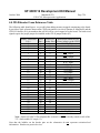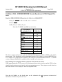
1
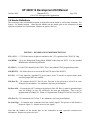
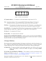
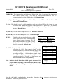
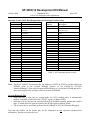
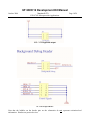
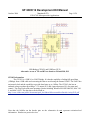
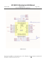
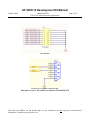
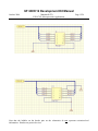
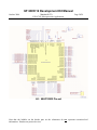
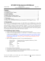
UF 68HC12 Development Kit Manual
(Version 4.01)
EEL 4744: Microprocessor Applications
October 2006
Page 1/24
Contents
1.0 Introduction................................................................................................................ 1
2.0 Installation & Quick Testing ....................................................................................... 1
3.0 Header Definitions..................................................................................................... 1
4.0 Jumper Definitions..................................................................................................... 3
5.0 Memory Map & Interrupt Vectors............................................................................... 5
6.0 CPLD/Header Cross Reference Table ...................................................................... 7
7.0 Schematics................................................................................................................ 8
A.1 68HC12B32 Pin-out ................................................................................................ 19
A.2 Altera 7064 – EPROM/EEPROM Decode Equations & CPLD Signal Pin-outs ....... 23
1.0 Introduction
The UF 68HC12 Development Kit integrates the 68HC12B32 with an EPROM and an Altera 7064
CPLD. The purpose of the EPROM is to allow expanded mode booting of the 6812 using the UF-6812
Monitor/Debugger, D-Bug4744 (similar to Motorola’s D-Bug12). I/O can be easily connected to the
processor via address decoding in the CPLD. These features, coupled with the fact that the 6812’s
address, data, control and port pins are broken out to 100 mil headers, provide a fast and easy platform
for prototyping of hardware with the 68HC12B32 Micro-controller.
2.0 Installation & Quick Testing
1. Connect a USB cable between the 6812 Development board and your PC.
2. Connect a 5V power supply to Header J11. Note: Pin1 is +5V and Pin3 is Ground. See Figure
1 for the location of Header J11. * Note: Alternatively, you may power your 6812HC12 board
using the power supplied from your computer via the USB cable. To enable this, short solder
across the jumper labeled RP. DO NOT CONNECT BOTH POWER SUPPLIES AT THE
SAME TIME!*
3. Open a terminal application on your PC. Set your terminal properties to:
Connect Using:
Transfer Rate:
Data Bits:
Parity:
Stop Bits:
Flow Control:
Communication Port Assigned to USB Port (e.g. Com1)
9600 bits per second
8
None
1
None
4. Press the Reset Button on the Board.
5. You should now see the monitor menu show up in your terminal.
6. If you do not see this menu in your terminal application, check all of your board’s jumper
settings using the definitions in the next section.
Note that the bubbles on the header pins on the schematics do not represent activation-level
information. Headers are passive devices.
UF 68HC12 Development Kit Manual
(Version 4.01)
EEL 4744: Microprocessor Applications
October 2006
Page 2/24
3.0 Header Definitions
This section provides a detailed description of the headers on the board as well as their functions. See
Figure 1 for header location. (Note that the bubbles on the header pins on the schematics do not
represent activation-level information. Headers are passive devices.)
FIGURE 1. HEADER AND JUMPER DEFINITIONS
J15 (+3.3V) - +3.3V Header where all pins are attached to the 3.3V regulator of the CP2103 IC chip.
J14 (BDM) – J14 is the Background Debug Mode (BDM) header from the HC12. It is the standard
BDM header as defined by Motorola.
J2 (JTAG) – J2 is the JTAG header for the CPLD. This is the standard JTAG programming header.
J10 (RX/TX) – J10 allows the user to access the RX and TX pins of the HC6812.
J11 (5V) – J11 is the input for a regulated 5V power source. Note: To use this as a power input, make
sure that jumper RP is not enabled.
J18 (Port P) – J18 contains the 6812’s Port W pins. This port is also referred to as Port P in some
Motorola documentation. See schematics for exact pin definitions.
J4 (Port AD) – J4 contains the 6812’s analog-to-digital port, Port AD. Bits 1:0 must be grounded upon
reset for D-Bug12 to run. See schematics for exact pin definitions. This is not yet
implemented in D-Bug4744. When it is implemented, D-Bug4744 will use Port AD, bit
7.
J22 (Port T) – J22 contains the 6812’s Port T. See schematics for exact pin definitions.
J6 (Cntl Sigs) – J6 contains some commonly used bus control signals. The pin-out of this header is
shown in Figure 2. (- denotes an active low signal)
Note that the bubbles on the header pins on the schematics do not represent activation-level
information. Headers are passive devices.
UF 68HC12 Development Kit Manual
October 2006
(Version 4.01)
EEL 4744: Microprocessor Applications
GND
GND
- IRQ
DBE
GND
ECLK
GND
GND
R/W
-Reset
Page 3/24
Figure 2. Header J6 Pin Definitions
J17 (Latched Address) – J17 contains the 16 bit latched address output from the 74373’s.
Note: In previous semesters, 374’s were used with ECLK tied to the CP input. 373’s however,
eliminate the need for a delayed ECLK, but they require #ECLK for the latch enable.
J30 (Data) – J30 contains the 8 bit data I/O pins from the 6812. This header is not buffered and is
connected directly to the 6812, therefore it also contains the raw upper 8 bit address.
J16 (CPLD I/O) – J16 contains all the CPLD I/O lines for general purpose use including CPLD special
function input pins 1 (input/CLR), 2 (input/CLK2), 43 (input/CLK1), and 44 (input/OE1)..
J31 (Port S) – J31 contains the 6812’s Port S.
J32 (Port DLC) – J32 contains the 6812’s Port DLC.
J25 A/B and J26 A/B (EPROM & EEPROM) – Jumpers are used to select between using EPROM or
EEPROM in socket U1. These are implemented as the footprints of surface mount resitors. Connecting
the pads with solder is the equivalent of installing a jumper.
4.0 Jumper Definitions
This section provides a detailed description of the jumpers on the board as well as their functions. See
Fig. 1. Jumpers are implemented as the footprints of surface mount resistors. To connect or disconnect
a signal, simply drag a trace of solder across the pads or break said trace with a hot soldering iron.
J1 (ROM OE) – J1 connects the ROM’s output enable signal (OE) to the CPLD via pin 26 on the
CPLD. If this jumper is removed, the ROM’s OE signal is left floating. Default:
Connected
J25 A/B and J26 A/B (EPROM & EEPROM) – These jumpers are used to select between using
EPROM or EEPROM in socket U1. For EPROM, J25 B and J26 B should be connected. For
EEPROM, J25 A and J26 A should be connected. Default: EPROM
Note that the bubbles on the header pins on the schematics do not represent activation-level
information. Headers are passive devices.
UF 68HC12 Development Kit Manual
October 2006
(Version 4.01)
EEL 4744: Microprocessor Applications
Page 4/24
J20 (BKGD) – This jumper selects the Background Debug Mode. Note: If you install this jumper, you
must remove it after reset. This must be done because BKGD is also as a
communication line in the BDM header (J14). Default: Open
(Vfp) – Flash Programming Jumper. If installed, connects +12V from Header J10 to VFP
pin on 6812. Default: Open
J3 (SA) – This header is used to enable standalone mode on the board. When this jumper is open,
PLDC0 is high. When the jumper is connected, PLDC0 is pulled low. The Monitor
program can be edited to poll this signal and begin a running pre-described code in
memory. Default: Open
J9 (MOD A) – J9 is the Mode A input to the HC12. Default: Connected
J8 (MOD B) – J8 is the Mode B input to the HC12. Default: Open
RP (PS) –
This allows the user to select between which
power input will be used. If an unregulated
power source is used via header J10, RP
must be disconnected. If you wish to power
the board through the USB cable, RP
should be connected. Default: Open
Power Source J7
Reg 5V on J11 Unconnected
USB
Connected
Figure 3. J7 Definition
J5 (CPLD Jumpers) – J5 contains a variety of control signals to
connect to the CPLD. Each signal is labeled on the
board next to the pin it controls. When the jumpers are
connected the signals are connected to the CPLD pins
according to Figure 3. All the address signals come
from the latched address source, thus, they are not the
raw address signals. Typically, all the jumpers are
installed except those on XIRQ and IRQ.
Note: Students should determine which signals to connect for
proper memory decoding of the EPROM/EEPROM in the
memory map. All decoding circuitry is found in the
CPLD.
6812 Signal CPLD Pin
DBE
21
A12
20
A13
19
A14
18
A15
17
Reset
16
R/W
14
ECLK
12
XIRQ
11
IRQ
9
Figure 4. J5 Connections
Note that the bubbles on the header pins on the schematics do not represent activation-level
information. Headers are passive devices.
UF 68HC12 Development Kit Manual
October 2006
(Version 4.01)
EEL 4744: Microprocessor Applications
Page 5/24
5.0 Memory Map & Interrupt Vectors
Single Chip Mode
Address (Hex)
0-1FF
800-BFF
D00-FFF
8000-FFFF
Devices
6812 Internal Registers
1K Internal SRAM
768 Bytes of Internal EEPROM
*32K Bytes Flash Memory (~100 Writes Only)
Expanded Mode
Address (Hex)
0-1FF
800-BFF
D00-FFF
8000-FFFF
*Note:
Devices
6812 Internal Registers
1K Internal SRAM
768 Bytes of Internal EEPROM
*External 32K space. We added an 8K EPROM from E000-FFFF.
Lower 8K in Single Chip Mode is the same as the lower 8K in Expanded Mode. The upper
32K in Single Chip Mode is Flash Memory and in Expanded Mode this area is open for
attaching new devices (which is why we chose to place EPROM here).
Internal SRAM in both Single-Chip and Expanded Modes
Address (Hex)
800-88F
890-8FF
900-BDF
BE0-BFF
Explanation
Pseudo-vector locations and variables in Internal SRAM (approx.)
Internal SRAM available to user with D-Bug4744 (I usually use
this for my stack)
Internal SRAM available to user with D-Bug4744
D-Bug4744 stack space
CPLD ROM Decoder Logic Equation: ROM_OE = ~RESET * RW * ECLK * A15 *A14 *A13
Note that OE, RESET, and DBE are active-low and RW = R(H) = W(L) = R/~W . When you
build the circuit to create this equation, remember that activation level mismatches create NOTs
for free. The ROM will only send outputs to the data pins during read operations when DBE is
true and the addresses are appropriate for the ROM (from $E000-$FFFF).
Note that the bubbles on the header pins on the schematics do not represent activation-level
information. Headers are passive devices.
UF 68HC12 Development Kit Manual
October 2006
(Version 4.01)
EEL 4744: Microprocessor Applications
Page 6/24
Interrupt Vectors (6812 Hard Designations) and Interrupt Pseudo-vectors
Address (Hex)
FF80-FFC1
FFC2-FFC9
FFCA, FFCB
FFCC, FFCD
FFCE, FFCF
FFD0, FFD1
FFD2, FFD3
FFD4, FFD5
FFD6, FFD7
FFD8, FFD9
FFDA, FFDB
FFDC, FFDD
FFDE, FFDF
FFE0, FFE1
FFE2, FFE3
FFE4, FFE5
FFE6, FFE7
FFE8, FFE9
FFEA, FFEB
FFEC, FFED
FFEE, FFEF
FFF0, FFF1
FFF2, FFF3
FFF4, FFF5
FFF6, FFF7
FFF8, FFF9
FFFA, FFFB
FFFC, FFFD
FFFE, FFFF
Devices
Reserved for future use
Reserved for mfg. test
Pulse Accumulator B
Overflow
Modulus Down Counter
Underflow
Reserved for mfg. test
BDLC
Analog-to-Digital
Reserved
SCI #0
SPI Serial Transfer Complete
Pulse Accumulator Input Edge
Pulse Accumulator Overflow
Timer Overflow
Timer Channel #7
Timer Channel #6
Timer Channel #5
Timer Channel #4
Timer Channel #3
Timer Channel #2
Timer Channel #1
Timer Channel #0
Real Time Interrupt
IRQ
XIRQ
SWI
Reserved for the Future
COP Failure Reset
Clock Monitor Failure Reset
*Reset
Pseudo-Vector
Address
$0809-$080B
$080C-$080E
$080F-$0811
$0812-$0814
$0815-$0817
$0818-$081A
$081B-$081D
$081E-$0820
$0821-$0823
$0824-$0826
$0827-$0829
$082A-$082C
$082D-$082F
$0830-$0832
$0833-$0835
$0836-$0838
$0839-$083B
*$FF6C
$083F-$0841
$0842-$0844
$0845-$0847
*$FF80
Interrupt Pseudo-Vector
Description
Analog-to-Digital
Serial Communications
Interface (SCI)
Serial Peripheral Interface
(SPI)
Pulse Accumulator Input Edge
Pulse Accumulator Overflow
Timer Overflow
Timer Channel 7
Timer Channel 6
Timer Channel 5
Timer Channel 4
Timer Channel 3
Timer Channel 2
Timer Channel 1
Timer Channel 0
Real Time Interrupt (RTI)
IRQ
XIRQ
Software Interrupt (SWI)
Unimplemented Opcode Trap
COP Failure Reset
Clock Monitor Failure Reset
Reset
Table 2. 6812 interrupt pseudo-vectors.
Table 1. 6812 interrupt vectors.
Note: On the UF 68HC12 Development Kit, the addresses in FFFE & FFFF in external (added on)
EPROM point to the external EPROM location of the D-Bug4744 (UF-6812
Monitor/Debugger) Thus at this location in EPROM there is a vector that is loaded into the PC
that causes program flow to begin at the first location in EPROM.
General Hints and Tips
• When the 6812 is reset into any normal mode, the COP watchdog timer is automatically
enabled. To disable it write $00 to the COPCTL register at address $0016.
• When the 6812 is reset into any normal mode the R/W disabled externally and the pin is pulled
high. To enable the R/W signal write $04 to the PEAR register at address $000A
• The two items above are already performed in the D-Bug4744 (UF-6812 Monitor/Debugger)
Note that the bubbles on the header pins on the schematics do not represent activation-level
information. Headers are passive devices.
UF 68HC12 Development Kit Manual
(Version 4.01)
EEL 4744: Microprocessor Applications
October 2006
Page 7/24
6.0 CPLD/Header Cross Reference Table
The following table should prove very useful when adding memory-mapped components to the board.
It provides a quick reference between the CPLD pin numbers (as seen in Quartus or MaxPlusII) and the
CPLD I/O header (J16) pin numbers that will be will be wire-wrapped to on the board. The hard-wired
signals require the proper jumper be installed on the CPLD jumper header (J5).
Quartus / MaxPlusII CPLD CPLD I/O
Hard-wired Signal & Type
I/O #
Pin # Header Pin # (if any) relative to the CPLD
1
4
1
UART_TX_in
2
5
3
3
6
5
4
8
7
5
9
9
IRQ , Output
6
11
11
7
8
9
10
11
12
13
14
15
16
17
18
19
20
21
22
23
24
25
26
27
28
12
14
16
17
18
19
20
21
24
25
26
27
28
29
31
33
34
36
37
39
40
41
13
15
17
19
21
23
25
27
28
26
24
22
20
18
16
14
12
10
8
6
4
2
XIRQ ,
Output
ECLK, Input
R/ W , Input
RESET , Input
A15, Input
A14, Input
A13, Input
A12, Input
DBE , Input
ECLK , Output
Boot ROM Enable, Output
UART_TX_Out
Note: On the UF 68HC12 Development Kit version 4.0, ECLK is already routed to each of the
373’s latch enable (LE on pin 11).
Note that the bubbles on the header pins on the schematics do not represent activation-level
information. Headers are passive devices.
UF 68HC12 Development Kit Manual
October 2006
(Version 4.01)
EEL 4744: Microprocessor Applications
Page 8/24
J16 : CPLD IO Header Pin-out
Note that the bubbles on the header pins on the schematics do not represent activation-level
information. Headers are passive devices.
UF 68HC12 Development Kit Manual
(Version 4.01)
EEL 4744: Microprocessor Applications
October 2006
Page 9/24
7.0 Schematics
Address Latches (74F373’s are actually used, not 74LS373’s). Pin 11
(marked C) is the latch enable (LE)
Note that the bubbles on the header pins on the schematics do not represent activation-level
information. Headers are passive devices.
UF 68HC12 Development Kit Manual
October 2006
(Version 4.01)
EEL 4744: Microprocessor Applications
Page 10/24
J15 : 3.3V Regulated output
J6 : Control Signal Header
Note that the bubbles on the header pins on the schematics do not represent activation-level
information. Headers are passive devices.
UF 68HC12 Development Kit Manual
October 2006
(Version 4.01)
EEL 4744: Microprocessor Applications
Page 11/24
USB Bridge (CP2103) and USB Port (JP 23)
Alternative access to TX and RX are found on J10 and PS0, PS1
CP2103 Information
The CP2103 is a USB 2.0 to UART Bridge. It is has the capability of taking full-speed data
(12Mbps) from a USB cable and converting this data to serial using the internal UART. The UART has
an internal clock and the capability to provide baud rates up to 1 Mbits. The CP2103 also has an
onboard voltage regulator providing a 3.3V output (J15) and 4 general purpose IO’s for status and
control. The chip works with most operating systems including Windows®98 SE/2000/XP, MAC OS9, and MAC OS-X. The data sheet can be found at:
http://www.silabs.com/public/documents/tpub_doc/dsheet/Microcontrollers/Interface/en/cp2103.pdf
Note that the bubbles on the header pins on the schematics do not represent activation-level
information. Headers are passive devices.
UF 68HC12 Development Kit Manual
October 2006
(Version 4.01)
EEL 4744: Microprocessor Applications
Page 12/24
CPLD Pin Layout
Note that the bubbles on the header pins on the schematics do not represent activation-level
information. Headers are passive devices.
UF 68HC12 Development Kit Manual
October 2006
(Version 4.01)
EEL 4744: Microprocessor Applications
Page 13/24
J30 : Data Bus
Serial Port Circuit (DB9- Used in later labs)
Alternative access to TX and RX are found on J10 and PS0, PS1
Note that the bubbles on the header pins on the schematics do not represent activation-level
information. Headers are passive devices.
UF 68HC12 Development Kit Manual
October 2006
(Version 4.01)
EEL 4744: Microprocessor Applications
Page 14/24
EEPROM (28C64 or 28C256) or EPROM (27C256 or 27C64)
Note that the bubbles on the header pins on the schematics do not represent activation-level
information. Headers are passive devices.
UF 68HC12 Development Kit Manual
October 2006
(Version 4.01)
EEL 4744: Microprocessor Applications
Page 15/24
Note that the bubbles on the header pins on the schematics do not represent activation-level
information. Headers are passive devices.
UF 68HC12 Development Kit Manual
October 2006
(Version 4.01)
EEL 4744: Microprocessor Applications
Page 16/24
J18 : Port P
J31 : Port S
Note that the bubbles on the header pins on the schematics do not represent activation-level
information. Headers are passive devices.
UF 68HC12 Development Kit Manual
October 2006
(Version 4.01)
EEL 4744: Microprocessor Applications
Page 17/24
J22 : Port T
Note that the bubbles on the header pins on the schematics do not represent activation-level
information. Headers are passive devices.
UF 68HC12 Development Kit Manual
October 2006
(Version 4.01)
EEL 4744: Microprocessor Applications
Page 18/24
J17 : Address Bus
Note that the bubbles on the header pins on the schematics do not represent activation-level
information. Headers are passive devices.
UF 68HC12 Development Kit Manual
October 2006
(Version 4.01)
EEL 4744: Microprocessor Applications
Page 19/24
Reset Circuitry
Stand-Alone Jumper and Background Jumper
Note that the bubbles on the header pins on the schematics do not represent activation-level
information. Headers are passive devices.
UF 68HC12 Development Kit Manual
October 2006
(Version 4.01)
EEL 4744: Microprocessor Applications
Page 20/24
U4 : 68HC12B32 Pin-out
Note that the bubbles on the header pins on the schematics do not represent activation-level
information. Headers are passive devices.
UF 68HC12 Development Kit Manual
October 2006
(Version 4.01)
EEL 4744: Microprocessor Applications
Page 21/24
The following figures are magnified sections of the 68HC12 schematic:
To Port S Header
To Port T, S, AD
Note that the bubbles on the header pins on the schematics do not represent activation-level
information. Headers are passive devices.
UF 68HC12 Development Kit Manual
October 2006
(Version 4.01)
EEL 4744: Microprocessor Applications
Page 22/24
Port E Pins
Shared Address and Data Bus
Note that the bubbles on the header pins on the schematics do not represent activation-level
information. Headers are passive devices.
UF 68HC12 Development Kit Manual
October 2006
(Version 4.01)
EEL 4744: Microprocessor Applications
Page 23/24
Note that the bubbles on the header pins on the schematics do not represent activation-level
information. Headers are passive devices.
UF 68HC12 Development Kit Manual
(Version 4.01)
EEL 4744: Microprocessor Applications
October 2006
Page 24/24
A.2 Altera 7064 – EPROM/EEPROM Decode Equations & CPLD Signal Pinouts
Required EPROM/EEPROM Equations for 8k device at $E000-$FFFF:
ROM_CE = RESET * RW * ECLK * A15 * A14 *A13
ECLK = ECLK
UART_TX_in = UART_TX_out
Note that CE, RESET, and DBE are active-low.
Pin Name &
Activation Level
ROM_CE(L)
RESET
RW
[=R/ W =R(H)=W(L)]
DBE
A15(H)
A14(H)
A13(H)
ECLK
ECLK
UART_TX_in
UART_TX_out
CPLD Pin #
26
16
14
21
17
18
19
12
24
4
41
The above equation and pin-outs enable the EPROM/EEPROM from $E000 to $FFFF in the 6812’s
memory map. This information can be programmed into the CPLD either as a circuit (BDF/GDF file)
or as VHDL code (with filename extension .vhd) using the Quartus/MaxPlusII software. A student
version of Quartus/MaxPlusII is available (for free) at http://www.altera.com.
Programming Note (using Byte Blaster cable and JTAG header on board):
When programming the CPLD, remove all of the jumpers between the processor and the CPLD so that
signals from the processor can't interfere in the programming process. These jumpers can be found on
the header labeled “CPLD Jumpers” on the development board.
Note that the bubbles on the header pins on the schematics do not represent activation-level
information. Headers are passive devices.