1
Electrical characteristics
5.3.17
STM32F103xx
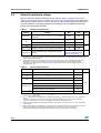
12-bit ADC characteristics
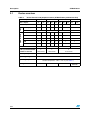
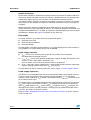
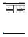
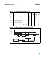
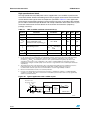
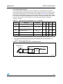
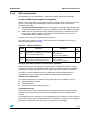
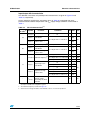
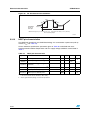
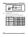
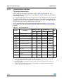
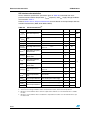
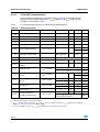
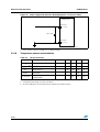
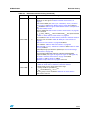
Unless otherwise specified, the parameters given in Table 44 are derived from tests
performed under ambient temperature, fPCLK2 frequency and VDDA supply voltage
conditions summarized in Table 7.
Note:
It is recommended to perform a calibration after each power-up.
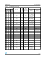
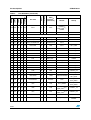
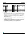
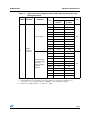
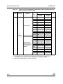
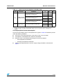
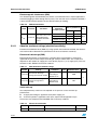
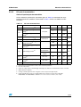
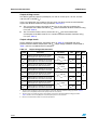
Table 44.
ADC characteristics
Symbol
Parameter
Conditions
Min
Typ
Max
Unit
VDDA
ADC power supply
2.4
3.6
V
VREF+
Positive reference voltage
2.4
VDDA
V
IVREF
Current on the VREF input pin
220(1)
µA
fADC
ADC clock frequency
0.6
14
MHz
fS(2)
Sampling rate
0.05
1
MHz
823
kHz
17
1/fADC
VREF+
V
fTRIG(2)
VAIN
External trigger frequency
160(1)
fADC = 14 MHz
0 (VSSA or VREFtied to ground)
Conversion voltage range(3)
RAIN(2)
External input impedance
RADC(2)
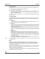
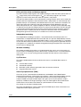
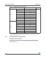
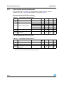
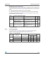
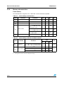
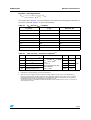
See Equation 1 and Table 45
kΩ
Sampling switch resistance
1
kΩ
CADC(2)
Internal sample and hold
capacitor
5
pF
tCAL(2)
Calibration time
fADC = 14 MHz
5.9
µs
83
1/fADC
0.214
tlat(2)
Injection trigger conversion
latency
fADC = 14 MHz
tlatr(2)
Regular trigger conversion
latency
fADC = 14 MHz
tS(2)
Sampling time
fADC = 14 MHz
tSTAB(2)
Power-up time
(4)
3
Total conversion time
(including sampling time)
µs
2(4)
1/fADC
0.107
17.1
µs
1.5
239.5
1/fADC
1
µs
18
µs
0
fADC = 14 MHz
1/fADC
0.143
1
tCONV(2)
µs
0
14 to 252 (tS for sampling +12.5 for
successive approximation)
1/fADC
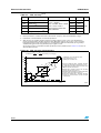
1. Data based on characterization results, not tested in production.
2. Guaranteed by design, not tested in production.
3. VREF+ can be internally connected to VDDA and VREF- can be internally connected to VSSA, depending on the package.
Refer to Section 3: Pin descriptions for further details.
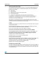
4. For external triggers, a delay of 1/fPCLK2 must be added to the latency specified in Table 44.
64/84