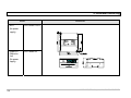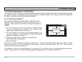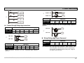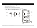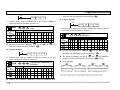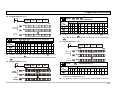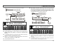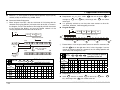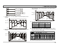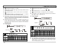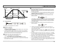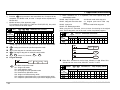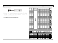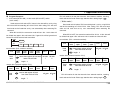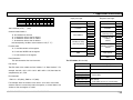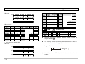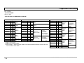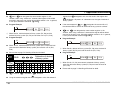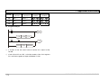
1
Table of Contents Appendix A: Communication Function Explanation .........A-1 1. Instruction and Inspections ................................................1-1 1.1. Model Explanation and Peripherals ..........................1-1 1.2. Product Profile and Outline ........................................1-3 1.3. Model Numbers ...........................................................1-4 Appendix B: EC Declaration of Conformity .......................B-1 2. Standard Specifications ......................................................2-1 3. Special Devices ...................................................................3-1 3.1. Special Auxiliary Relays .............................................3-1 3.2. Special Data Registers ...............................................3-2 3.3. High Speed Counters..................................................3-3 4. Installation and Wiring ........................................................4-1 4.1. Dimension and Terminals ...........................................4-1 4.2. Terminal Wiring ............................................................4-7 4.3. PLC Mounting Arrangements and Wiring Notes . 4-10 4.4. Wiring Guidelines ..................................................... 4-14 5. Initial PLC Start-Up..............................................................5-1 6. Basic Instructions ................................................................6-1 7. Application Instructions .......................................................7-1 WARNING " Always read this manual thoroughly before using DVP PLC. " AC input power must be disconnected before any maintenance. " This is an OPEN-TYPE PLC. The PLC must be placed in an enclosure to meet the safety approval of IEC 61131-2 and UL 508. " The PLC should be kept in an enclosure away from high temperatures, humidity, vibration, corrosive gas, liquid, airborne dust and metallic debrise. " Do not connect the AC main circuit power supply to any of the input/output terminals, as it will damage the PLC. Ensure all the wiring prior to power up. " Disconnect all power. Wait one minute for capacitors to discharge before touching internal circuit. " Some models are equipped with DC power supply output, do not exceed its rated output power. " Make sure the PLC is properly grounded any electromagnetic noise. 8. EX MPU and I/O Extension Units .....................................8-1 9. Troubleshooting and Fault Information ............................9-1 10. Additional Special Devices and Instructions ................ 10-1 10.1. New Special M and D Devices............................. 10-1 10.2. New Application Instructions ................................ 10-4 , to avoid 1. Introduction and Inspections 1.1. Model Explanation and Peripherals Thank you for choosing DELTA’ s PLC DVP Series. The DVP Series has main processing units and extension units. The main processing units offer 14-60 points and the extension units offer 8-32 points. The maximum input/o utput can be extended up to 128 points. It also can be used on applications according to INPUT/OUTPUT points, power sources, output modules, digital/analog exchanges (A/D & D/A converter). In addition, DVP SS Series has the special modules (AD/DA/PT/TC/XA) used for extending its functions and the maximum special modules can be extended up to 8 units. For more information on the DVP SS Series, refer to the DVP SS Series user manual. DVP ES/EX/SS MPU is made from improving the functions and specifications of R/T model structure. The additional R2/T2 model has wide improvement in commands type and execution speed. Please refer to the detail information about usable application commands and devices in this manual when using R2/T2 model. The specification in this manual is major for R2/T2 model so that there are some new commands and functions won’ t be provided for R/T model. Nameplate Explanation PLC Model Input Power Supply Specification Output Module Specification Control Code and Serial Number MCU Version V5.5 Serial Number Explanation Production number Production week Production year 2003 Production factory (TaoYuan Plant) Version type Production model © DELTA ELECTRONICS, INC. ALL RIGHTS RESERVED 1-1 1. Introduction and Inspections Model Explanation DVP Product Series: DVP Series Inputs+Outputs points / unit: 08~60points Models E : Main Processing Unit (Base Unit) X : Extension Unit S : S-TYPE Main Processing Unit Model Types 2 2 : Upgrade Model R : Relay T : Transistor N : No Output Module 00 AC Input H TYPE 01 DC Input L TYPE 11 DC Input H TYPE S : Standard X : A/D, D/A Functions C : Inextensible M : Digital Input (X input extend) N : Digital Output (Y output extend) P : Digital Input/Output (X/Y extend) Peripheral Equipment Ϩʳ DVPHPP: Handheld Programming Panel Ϩʳ WPLSoft: Windows Ladder Logic Programming Software Ϩʳ DPLSoft: DOS Ladder Logic Programming Software Ϩʳ DVPACAB115: 1.5M Cable (HPP PLC, DVPHPP has this cable attached) Ϩʳ DVPACAB215: 1.5M Cable (PC (9 PIN & 25 PIN D-SUB) PLC) Ϩʳ DVPACAB230: 3M Cable (PC (9 PIN & 25 PIN D-SUB) PLC) Ϩʳ DVPACAB2A30: 3M Cable (PC (9 PIN D-SUB) PLC) Ϩʳ DVPACAB230: 3M Cable (PC PLC) Ϩʳ DVPACAB315: 1.5M Cable (HPP PC) Ϩʳ DVPACAB403: 30cm Cable (MPU-main processing unit Extension Unit or Extension Unit extension cable) Ϩʳ DVPAADP01: HPP Power Supply (DVPACAB315 is attached) 1-2 Extension Unit I/O signal © DELTA ELECTRONICS, INC. ALL RIGHTS RESERVED 1. Introduction and Inspections 1.2. Product Profile and Outline Fig. 1-1: Features of the DVP PLC 1 DIN rail clip 2 DIN rail (35mm) 10 3 11 12 I/O terminal cover 5 Direct mounting holes Programming port cover (RS-232) Extension port Output indicators Status indicators, POWER, RUN ERROR I/O terminal cover 13 I/O terminal nameplate panel 6 I/O terminals 14 I/O terminal nameplate panel 7 8 I/O terminals Input indicators 15 RS-485 Communication port 4 9 © DELTA ELECTRONICS, INC. ALL RIGHTS RESERVED 1-3 1. Introduction and Inspections 1.3. Model Numbers Ϩʳ Standard MPU-00 Model DVP14ES00R2 DVP24ES00R2 DVP32ES00R2 DVP60ES00R2 DVP14ES00T2 DVP24ES00T2 Power 100~240VAC Input / Output Input Unit Output Unit Point Type Point Type 8 16 16 36 8 16 DC Sink or Source 6 8 16 24 6 8 DVP32ES00T2 16 16 DVP60ES00T2 36 24 Profile Profile reference Relay Transistor Ϩʳ Standard MPU-01 Model DVP14ES01R2 DVP24ES01R2 DVP32ES01R2 DVP14ES01T2 DVP24ES01T2 DVP32ES01T2 Power 24VDC Input / Output Input Unit Output Unit Point Type Point Type 8 6 16 8 Relay DC Sink 16 16 or 8 6 Source Transistor 16 8 16 16 Profile 1. Sink or Source connections. Please refer to Chapter 4 Installation and Wiring. 2. Please refer to Chapter 2 Standard Specifications for detailed electrical specifications. 1-4 © DELTA ELECTRONICS, INC. ALL RIGHTS RESERVED 1. Introduction and Inspections Ϩʳ Special Function MPU–00 Model Power DVP20E X00R2 Point DI AI 8 4 DC Sink or Source 100~240VAC DVP20E X00T2 Input / Output Input Unit Type DI AI 8 Point DO AO 6 2 6 2 -20mA~20mA -10V ~ +10 V 4 Output Unit Type DO AO Profile reference 0~20mA or -10V ~ +10 V (for R/T model) 0V ~ +10 V Transistor (for R2/T2 model) Relay Ϩʳ Analog/Digital MPU–11 Model Power DVP20E X11R2 Point DI AI 8 4 8 Point DO AO 6 DC Sink or Source 24VDC DVP20E X11T2 Input / Output Input Unit Type DI AI 0~20mA 0V ~ +10 V 6 DIΰDigital Inputα DOΰDigital Outputα AIΰAnalog Inputα AOΰAnalog Outputα Profile reference Relay -20mA~20mA -10V ~ +10 V 4 © DELTA ELECTRONICS, INC. ALL RIGHTS RESERVED 2 Output Unit Type DO AO 2 Transistor 1-5 1. Introduction and Inspections Ϩʳ Module Standard MPU–11 Model Power Point DVP14SS11R2 Input / Output Input Unit Type 8 Output Unit Point Type 6 DC Sink or Source 100~240VAC DVP14SS11T2 Profile reference Relay Transistor 6 8 Ϩʳ Digital I/O Extension Unit-00 Model Power Point Input / Output Input Unit Type Output Unit Point Type DVP24XN00R 0 24 DVP24XP00R 16 8 DVP32XP00R 16 DVP24XP00T 100~240VAC 16 DC Sink or Source Profile reference Relay 16 8 DVP24XN00T 0 24 DVP32XP00T 16 16 Transistor 1. Sink or Source connections. Please refer to Chapter 4 Installation and Wiring. 2. Please refer to Chapter 2 Standard Specifications for detailed electrical specifications. 1-6 © DELTA ELECTRONICS, INC. ALL RIGHTS RESERVED 1. Introduction and Inspections Ϩʳ Digital I/O Extension–01 (L-Type) Model Input Unit Power Point Type Output Unit Point Type None DVP16XM 01N 16 0 DVP16XN01R 0 16 DVP24XN01R 0 24 DVP24XP01R 16 8 Profile reference Relay DVP32XP01R 24VDC 16 DC Sink or Source 16 DVP16XN01T 0 16 DVP24XN01T 0 24 DVP24XP01T 16 8 DVP32XP01T 16 16 Transistor 1. Sink or Source connections. Please refer to Chapter 4 Installation and Wiring. 2. Please refer to Chapter 2 Standard Specifications for detailed electrical specifications. © DELTA ELECTRONICS, INC. ALL RIGHTS RESERVED 1-7 1. Introduction and Inspections Ϩʳ Digital I/O Extension–11 (H-Type) Model Input Unit Power DVP08XM11N Point 8 DVP16XM 11N 16 0 DVP08XN11R 0 8 DVP16XN11R 0 16 DVP24XN11R 0 24 DVP08XP11R 4 4 DVP24XP11R DVP32XP11R DVP08XN11T 24VDC 16 16 0 Type Output Unit DC Sink or Source Point 0 Profile reference Type None Relay 8 16 8 DVP16XN11T 0 16 DVP24XN11T 0 24 DVP08XP11T 4 4 DVP24XP11T 16 8 DVP32XP11T 16 16 Transistor 1. Sink or Source connections. Refer to Chapter 4 Installation and Wiring for more information. 2. Refer to Chapter 2 Standard Specifications for detailed electrical specifications. 3. When connects to DVP08XP11R/T, recommend to place at the end of extension units. Refer to Chapter 8 EX MPU and I/O Extension Units for more information. 1-8 © DELTA ELECTRONICS, INC. ALL RIGHTS RESERVED 1. Introduction and Inspections Ϩʳ Digital I/O Extension Units Model Input Unit Power Point Output Unit Type Point Type DVP08SM11N 8 0 None DVP08SN11R 0 8 Relay DVP08SN11T 0 8 Transistor DVP08SP11R 24VDC 4 DC Sink or Source Profile reference 4 Relay DVP16SP11R 8 8 DVP08SP11T 4 4 DVP16SP11T 8 8 Transistor ϨʳPlease refer to each user manual of extension model for the detail of SS special extension module. Ϩʳ Power Output Module Model Input Power Output Power DVPPS01 100~240VAC ΰ50/60Hzα Output Voltage: 24VDC Max. Output Current: 1A © DELTA ELECTRONICS, INC. ALL RIGHTS RESERVED Profile reference 1-9 2. Standard Specifications General Specifications Items Control Method I/O Processing Method Execution Speed Program Language Program Capacity Instructions General Auxiliary Relays Latched Specifications Stored program, cyclic scan system Batch I/O (refresh) Basic commands (severalӴs) Ladder Logic, Instruction, SFC 3792 STEPS 32 Basic sequential commands (Including STL / RET) 512+232 Points Direct I/O instruction available Application commands (10~hundredsӴs) Including the Step commands Built-in EEPROM 97 Application commands (145 including the 32-bit commands) M000~M511+ M768~M999 Special 256 Points 280 Points M512~M767 M1000~M1279 Step Relays (Latched) Initial Step Point 10 Points S0~S9 General Step Point 118 Points S10~S127 Timers Digital Counters Data registers Digital/Analog Remarks 64 Points T0~T63 (100ms time base) 63 Points T64~T126 (10ms time base, when M1028 is ON) 1 Points T127 (1ms time base) General Latched High-speed General 112 Points 16 Points 13 Points 1-Phase 5KHz, 2-Phase 5KHz 408 Points C0~C111 (16-bit counters) C112~C127 (16-bit counters) C235~C254 (all latched type, 32-bit counters) D0 ~ D407 Latched 192 Points D408~D599 Special 312 Points D1000~D1311 Aඎ D 4 Analog Input Channels 10-bit resolution (EX MPU only) 2 Analog Output Channels 8-bit resolution (EX MPU only) Dඎ A High Speed Pulse Output Pointers/Interrup P/I t Index Register E/F Decimal K Constants Hexadecimal H Serial Communication Protection Features Monitor / Debug 2 point (Y0, Y1), pulse output frequency: 10Hz to 10KHz P : 64 Points / I : 4 Points P0~P63 / I001, I101, I201, I301 2 Points E (=D1028), F (=D1029) 16-bit: -32768~+32767 32-bit: -2147483648~+2147483647 16-bit: 0000~FFFF 32-bit: 00000000~FFFFFFFF RS-232, RS-485 (2 Ports) Password, Execution Time, Illegitimate Command or Operand Execution time, Device setting © DELTA ELECTRONICS, INC. ALL RIGHTS RESERVED 2-1 2. Standard Specifications Electric Specifications 1 DVP14ES00ϭ Model Item DVP24ES00ϭ DVP32ES00ϭ DVP60ES00ϭ DVP20EX00ϭ DVP14ES01ϭ DVP24ES01ϭ DVP32ES01ϭ DVP20EX11ϭ Power Supply Voltage / Fuse 100~240VAC (-15%~10%), 50/60Hz ± 5% / 2 A / 250VAC 24VDC (-15%~10%) / 2 A / 250VAC Input Power Operating Characteristics Maximum Power Loss Time 95-100VAC is needed to start the PLC. If the voltage drops to 70VAC or less, the PLC will stop. 10ms or less A minimum of 18VDC is needed to start the PLC. If the voltage drops below 17.5VDC, the PLC will stop. 5ms or less Power Consumption DC24V Supply Current 20 VA 25VA 30VA 35VA 30 VA 400mA 400mA 400mA 200mA 400mA 5.5 W 6.5 W 8W 10 W Ϋ Ϋ Ϋ Ϋ Power Protection DC24V output short circuit Withstand Voltage 1500VAC(Primary-secondary), 1500VAC(Primary-PE), 500VAC(Secondary-PE) Insulation Resistance >5 MӨ at 500VDC (Between all inputs/outputs and earth) ESD: 8KV Air Dis charge EFT: Power Line: 2KV, Digital I/O: 1KV, Analog & Communication I/O: 250V Damped-Oscillatory Wave: Power Line: 1KV, Digital I/O: 1KV RS: 26MHz~1GHz, 10V/m The diameter of grounding wire cannot be smaller than the wire diameter of terminals L and N (All DVP units should be grounded directly to the ground pole). Operation: 0к~55к (Temperature), 50~95% (Humidity); Storage: -25к~70к (Temperature), 5~95% (Humidity) Pollution degree 2 Standard: IEC1131-2, IEC68-2-6 (Test Fc) / IEC 1131-2 & IEC68-2-27 (Test Ea) 400 552 580 750 536 260 414 430 386 Noise Immunity Grounding Environment Vibration /Shock Immunity Weight (g) Input Point Type Input Point Electric Specification Digit I/O Analog I/O (EX) Input Point Spec. DC (Sink or Source) 24VDC 5mA Input Voltage: -10V~+10V (Input Resistance: 40KO) Input Current: -20mA~+20mA(Input Resistance: 250O) Active Level OFFШON Above 10VDC Input Voltage Resolution: 10bit (Analog Input Resolution) ONШOFF Below 9VDC Input Current Resolution: 10bit Reaction Time About 10ms (Adjust D1020 and D1021 can 5ms (Adjusting D1118 can change reaction time) be 0~15ms) DC24V input polarity Output Point Electric Specification Output Point Type Relay-R Transistor-T Analog I/O (EX) Current Spec. 2A/1 point (5A/COM) 0.3A/1point (1.2 A/COM) 0~20mA Below 250VAC, Voltage Spec. 30VDC 0V~+10V 30VDC 100 VA (Inductive) 0.2W About 10ms OFFШON 20Ӵs ONШOFF 30Ӵs 10ms Ϋ Ϋ 8 bit 120 W (Resistive) Reaction Time Resolution 2-2 9W Maximum Load © DELTA ELECTRONICS, INC. ALL RIGHTS RESERVED 2. Standard Specifications Electric Specifications 2 Model DVPPS01 Item 100~240VAC (50/60Hz) Power Supply Voltage / Fuse Input Power Operating Characteristics Maximum Power Loss Time -- Power Consumption -- Insulation Resistance Noise Immunity Grounding Environment Vibration /Shock Immunity Weight (g) DVP14SS11R2/T2 DVP08SM11N DVP08SN11R/T DVP08SP11R/T DVP-16SP11R/T 24VDC (-15%~10%) (has power protect with opposite pole DC input) 5ms or less 2A / 250VAC 5W 8W ->5 MӨ at 500VDC (Between all inputs/outputs and earth) ESD: 8KV Air Discharge EFT: Power Line: 2KV, Digital I/O: 1KV, Analog & Communication I/O: 250V Damped-Oscillatory Wave: Power Line: 1KV, Digital I/O: 1KV RS: 26MHz~1GHz, 10V/m The diameter of grounding wire cannot be smaller than the wire diameter of terminals L and N (All DVP units should be grounded directly to the ground pole). Operation: 0к~55к (Temperature), 50~95% (Humidity); Storage: -25к~70к (Temperature), 5~95% (Humidity) Pollution degree 2 Standard: IEC1131-2, IEC68-2-6 (Test Fc) / IEC 1131-2 & IEC68-2-27 (Test Ea) 210 214/208 128 Input Point Type Input Point Electric Specification DC (Sink or Source) Output Point Type Input Current 24VDC 7mA Current Spec. Active Level OFFШON Above 10VDC ONШOFF Below 9VDC Voltage Spec. Reaction Time About 10ms (Adjust D1020 and D1021 can be 0~15ms) © DELTA ELECTRONICS, INC. ALL RIGHTS RESERVED Maximum Load Reaction Time 154 /146 141 /136 162 /154 Output Point Electric Specification Relay-R Transistor-T 55к 0.1A/1 point, 50к 0.15A/1 point 2A/1 point (5A/COM) 45к 0.2A/1 point, 40к 0.3A/1 point (2A/COM) Below 250VAC, 30VDC 30VDC 100 VA (Inductive) 7.2 W 120 W (Resistive) About 10ms OFFШON 15Ӵs, ONШOFF 25Ӵs 2-3 3. Special Devices 3.1. Special Auxiliary Relays Ϩʳ PLC Operation Status Ϩʳ Step Ladder Diagram M1000 M1001 M1002 M1003 Normally ON contact (a contact) Normally OFF contact (b contact) ON only for 1 scan after RUN OFF only for 1 scan after RUN M1040 M1041 M1042 M1043 Step transition inhibit Step transition start Start pulse Origin reset completed M1004 On when error occurs M1044 Origin condition M1008 M1009 M1010 Monitor timer flag (ON: PLC WDT time out) 24VDC down detection PLSY Y0 mode selection. ON: output continuously M1045 M1046 M1047 All outputs clear inhibit STL state setting STL monitor enable Ϩʳ Clocks M1011 M1012 M1013 M1014 Ϩʳ Flags M1019 M1020 M1021 M1022 M1023 M1024 M1025 M1028 M1029 M1030 M1070 M1031 M1032 M1033 M1034 M1039 Ϩʳ Interrupt Inhibit Setting 10msec clock 100msec clock 1sec clock 1min clock Cancel X0~X17 input delay Zero flag Borrow flag Carry flag PLSY Y1 mode selection. ON: output continuously System used Invalid communication request 10ms time base setting flag PLSY Y0 Instruction execution completed flag PLSY Y1 Instruction execution completed flag The Pulse unit switching (ON: 100 Ӵs) will be conducted at the PWM command. Non-holding memory all clear Holding memory all clear Memory holding at STOP All outputs disable Constant scan mode © DELTA ELECTRONICS, INC. ALL RIGHTS RESERVED M1050 I 001 masked M1051 I 101 masked M1052 I 201 masked M1053 I 301 masked Ϩʳ Error Flags M1060 CPU hardware error M1061 CPU internal malfunction (Flag) M1062 CPU internal malfunction (BIOS) M1063 CPU internal malfunction (RAM) M1064 Operator error M1065 Syntax error M1066 Program error M1067 Program execution error M1068 Execution error latch (ref. D1068) Ϩʳ PLC Operation Execution M1072 PLC RUN command execution M1073 Grammar inspection flag M1078 Y0 pulse output/stop control flag M1079 Y1 pulse output/stop control flag M1083 From / To mode exchange Ϩʳ RS-485 Communication M1120 Communication protocol holding M1121 Transmission ready M1122 M1123 M1124 M1125 M1126 Sending request Receiving completed Receiving wait Communication reset STX/ETX selection M1127 MODRD, RDST commands. Data receiving completed M1128 Transmitting / Receiving indication M1129 Receiving time out M1130 STX/ETX selection M1131=On during the conversion M1131 ( MODRD/RDST/MODRW data->HEX). M1140 MODRD / MODWR data received error M1141 MODRD / MODWR command error M1142 VFD-A command data received error M1143 ASCII / RTU mode selections M1161 8/16-bit mode setting Ϩʳ High Speed Counter (1-phase input) M1235 C235 counting mode (on: count down) M1236 C236 counting mode (on: count down) M1237 C237 counting mode (on: count down) M1238 C238 counting mode (on: count down) M1241 C241 counting mode (on: count down) M1242 C242 counting mode (on: count down) M1244 C244 counting mode (on: count down) Ϩʳ High Speed Counter (1-phase 2 inputs) M1246 C246 monitor (on: count down) M1247 C247 monitor (on: count down) M1249 C249 monitor (on: count down) Ϩʳ High Speed Counter (2-phase inputs) M1251 M1252 M1254 C251 monitor (on: count down) C252 monitor (on: count down) C254 monitor (on: count down) 3-1 3. Special Devices 3.2. Special Data Registers Ϩʳ PLC System Information D1000 Watchdog timer (WDT) value D 1001 DVP model no. + memory cap. /type D 1002 Program memory capacitor D 1003 D 1004 D 1005 D 1008 D 1010 D 1011 D 1012 D1020 D1021 D1022 D1025 D 1028 D 1029 D1030 D1031 D1032 D1033 D1038 Sum of program memory Error flag number System message Monitor the STEP position that occurs when timer time out Current scan time (unit: 0.1ms) Minimum scan time (unit: 0.1ms) Maximum scan time (unit: 0.1ms) X00~X07 input delay setting (0~15ms) X10~X17 input delay setting (0~15ms) AB phase counter mode selections Communication error code Index register E Index register F Output numbers of Y0 pulse (Low word) Output numbers of Y0 pulse (High word) Output numbers of Y1 pulse (Low word) Output numbers of Y1 pulse (High word) When PLC MPU is master, the setting of data response delay time. Time unit is 0.1ms. D1039 Constant scan time (unit: ms) Ϩʳ Step Ladder Diagram D 1040 ON state number 1 D 1041 ON state number 2 D 1042 ON state number 3 D 1043 ON state number 4 D 1044 ON state number 5 D 1045 ON state number 6 D 1046 ON state number 7 D 1047 ON state number 8 3-2 Ϩʳ Error Check D 1061 System detailed error code D 1065 Syntax error code D 1066 Loop error code D 1067 D 1068 D 1069 Ϩʳ A/D, D/AConversion (Only EX Model) D1056 Present value of analog input channel 0 (CH0) D1057 Present value of analog input channel 1 (CH1) D1058 Present value of analog input channel 2 (CH2) Algorithm error code Lock the algorithm error address D1059 Step number of errors associated with flags M1065~M1067 Ϩʳ System Usage D 1050 PLC will automatically convert the ASCII data saved in D1070~D1085 to HEX. Refer to chapter 7 D 1055 Application Commands for more information. D 1070 D 1085 D 1089 D 1099 D 1256 D 1295 D 1296 D 1311 When the PLC built-in RS-485 communication command receives feedback signals from receiver, the signals will be saved in the registers D1070~D1085. User can use the contents saved in the registers to check the feedback data. Refer to chapter 7 for more details. When the PLC built-in RS-485 communication command is executed, the transmitting signals will be stored in the registers D1089~D1099. User can use the contents saved in the registers to check the feedback data. Refer to chapter 7 for more details. ES: MODRW command of RS-485 is built-in. The characters that sent during executing is saved in D1256-D1295. User can check according to the content of these registers. (Using MOV, DMOV, BMOV to move the data in this area in version 4.9.) ES: PLC system will convert ASCII in the content of the register that user indicates to HEX. (Using MOV, DMOV, BMOV to move the data in this area in version 4.9.) D 1110 D 1111 D 1112 Present value of analog input channel 3 (CH3) Average of analog input channel 0 (CH 0) Average of analog input channel 0 (CH 1) Average of analog input channel 0 (CH 2) Average of analog input channel 0 (CH 3) Analog output channel 0 (CH 0) Analog output channel 1 (CH 1) For EX model only. It is the filter wave time setting between the A/D conversions, and with D1118 the default setting as 0 and the unit as 1ms, all will be regarded as 5ms if D1118Љ5 Ϩʳ PLC System Setting D 1119 System used (PLC operation mode) D1121 PLC communication address Ϩʳ RS-485 Serial Communication Port D1120 RS-485 communication protocol D1122 Residual words of transmitting data D1123 Residual words of receiving data D1124 Start character definition D1125 First ending character definition (ETX1) D1126 Second ending character definition (EXT2) D1129 RS-485 time-out setting (ms) D1130 MODBUS return error code record Ϩʳ Auxiliary System Check Information D 1136 System used (Error diagnosis) D 1137 Address of operator error occurs D1140 Special extension module number D 1141 System used (Self-diagnosis code) D 1142 Input points (X) of extension unit D 1143 Output points (Y) of extension unit D 1113 D 1116 D 1117 © DELTA ELECTRONCIS, INC. ALL RIGHTS RESERVED 3. Special Devices Additional Information M: Read Only Relay, can work as a contact yet cannot work as an output coil. But M1131and M1132 are used for system, they can’ t work as a contact or a output coil. D: Read Only Register. Here are the descriptions of the special devices, also refer to chapters 6 and 7 for more details. Device Descriptions Device Descriptions If the PLC receive an illegal communication service request when it is connected with an M1025 HPP, PC or HMI (Human-Machine-Interface), the M1025 will be set and save the error code in D1025. D1001 Users have access to where the software version is saved in Device D1001, e.g. D1001 = H 4027 is an indication of Version 2.7. HPP is utilized to read the data. When “Knnnnn” is displayed, simply press the <H> key to switch to the HEX display mode. OFF: the time base of timer T64~T126 is M1028 100ms. ON: the time base is 10ms. D1003 Sums up the memory content of the PLC. Users could use this data register to identify the internal program of the PLC. Used with the MODRD/MODWR commands: OFF: the ASCII mode M1143 ON: the RTU mode Error Code: 01: illegal command 02: illegal device command D1025 Device D1121 Saves the PLC communication addresses. This is a Latched Register. Identify the PLC operating mode: D1119 03: requested data exceeds the range 07: checksum error Descriptions 1: A/D operating mode 2: D/A operating mode 3: A/D, D/A operating mode 4: normal mode (DI/DO) 3.3. High Speed Counters Type Input X00 X01 X02 X03 C235 U/D C236 U/D 1-phase input C237 C238 C241 U/D R U/D U/D U: Increasing D: Decreasing C242 U/D R A: A-phase input B: B-phase input C244 U/D R S 1-phase 2 inputs C246 C247 C249 U U U D D D R R S 2-phase inputs C251 C252 C254 A A A B B B R R S S: Start input R: Clear input When high speed counters C235~C254 are in use, the inputs of the counter will be disabled for other use. Refer to chapter 7 Application Instructions for more details on API53 DHSCS and API54 DHSCR. © DELTA ELECTRONICS, INC. ALL RIGHTS RESERVED 3-3 4. Installation and Wiring 4.1. Dimension and Terminals Dimensions Model MPU Dimensions DVP14ES00 R2/T2 (Including power supply) IN POWER RUN ERROR Digital I/O Extension Unit OUT DVP 0 1 2 3 4 5 6 0 1 7 2 3 4 5 DVP16XM11N (No power supply) © DELTA ELECTRONCIS, INC. ALL RIGHTS RESERVED 4-1 4. Installation and Wiring Model MPU (Including power supply) DVP24ES00 R2/T2 DVP32ES00 R2/T2 DVP20EX00 R2/T2 MPU DVP20EX11 R2/T2 Dimensions (No power supply) Digital I/O Extension Unit DVP24XP00 R/T DVP24XN00 R/T DVP32XP00 R/T (Including power supply) Digital I/O Extension Unit (No power supply) 4-2 DVP16XN11 R/T DVP24XN11 R/T DVP24XP11 R/T DVP32XP11 R/T © DELTA ELECTRONCIS, INC. ALL RIGHTS RESERVED 4. Installation and Wiring Model MPU Dimensions DVP60ES00 R2/T2 (Including power supply) S/S X22 X23 X0 X25 X24 X1 X2 X27 X26 X3 X4 X30 X5 X32 X31 X6 X7 IN POWER RUN ERROR 24G © DELTA ELECTRONCIS, INC. ALL RIGHTS RESERVED Y0 Y1 C0 Y2 C1 Y3 C2 Y4 C3 Y5 C4 Y10 Y6 Y7 X35 X12 X36 X13 X37 X14 X40 X15 X41 X16 X17 X42 X43 X20 X21 5 6 7 10 11 12 13 14 15 16 17 0 1 2 3 4 5 6 7 10 11 12 13 14 15 16 17 20 21 22 23 24 25 26 27 Y11 C5 X34 X11 2 3 4 40 41 42 43 OUT DVP 60ES +24V X33 X10 0 1 20 21 22 23 24 25 26 27 30 31 32 33 34 35 36 37 Y12 Y14 Y13 Y15 C6 Y21 Y20 Y16 Y17 C7 Y24 Y22 Y23 Y25 C8 Y26 Y27 4-3 4. Installation and Wiring Model MPU Dimensions DVP14ES01 R2/T2 (No power supply) IN 0 1 2 3 4 5 6 POWER RUN ERROR Digital I/O Extension Unit OUT DVP 0 1 7 2 3 4 5 DVP16XM01N (No power supply) 4-4 © DELTA ELECTRONCIS, INC. ALL RIGHTS RESERVED 4. Installation and Wiring Model MPU (No power supply) Dimensions DVP24ES01 R2/T2 DVP32ES01 R2/T2 IN POWER RUN ERROR Digital I/O Extension Unit (No power supply) OUT DVP 0 1 2 3 4 5 6 7 10 11 12 13 14 15 16 17 0 1 2 3 4 5 6 7 10 11 12 13 14 15 16 17 DVP16XN01 R/T DVP24XP01 R/T DVP24XN01 R/T DVP32XP01 R/T © DELTA ELECTRONCIS, INC. ALL RIGHTS RESERVED 4-5 4. Installation and Wiring Model Digital I/O Extension Unit Dimensions DVP08XM11N DVP08XN11 R/T DVP08XP11 R/T (No power supply) POWER LV 0 1 2 3 4 5 6 7 DVP Logic Progammable Controller MODEL : 4-6 © DELTA ELECTRONCIS, INC. ALL RIGHTS RESERVED 4. Installation and Wiring 4.2. Terminal Wiring Terminal Layouts of the Standard Function MPU What follows is a complete display of the terminal wiring for all the model types within the DVP Series; refer to locations 13 and 14 on Figure 1 -1 of 1.2 Product Profile and Outline for detail. DVP60ES S/S X22 X23 X24 X25 X26 X27 X30 X31 X32 X33 X34 X35 X36 X37 X40 X41 X42 X43 X0 X1 X2 X3 X4 X5 X6 X7 X10 X11 X12 X13 X14 X15 X16 X17 X20 X21 00 ( AC Power IN, DC Signal IN ) Y0 Y1 Y2 Y3 Y4 Y5 C0 C1 C2 C3 C4 Y6 DVP32ES S/S Y10 Y11 Y14 Y15 Y20 Y21 Y24 Y25 Y7 C5 Y12 Y13 C6 Y16 Y17 C7 Y22 Y23 C8 Y26 Y27 S/S X10 X11 X12 X13 X14 X15 X16 X17 X0 X1 X2 X3 X4 X5 X6 X7 01 ( DC Power IN, DC Signal IN ) Y0 Y1 C0 Y2 DVP24ES 00 ( AC Power IN, DC Signal IN ) Y4 Y3 Y0 Y1 C0 Y2 S/S Y4 Y5 Y3 C1 Y6 Y10 Y11 Y14 Y15 Y7 C2 Y12 Y13 C3 Y16 Y17 S/S X10 X11 X12 X13 X14 X15 X16 X17 X0 X1 X2 X3 X4 X5 X6 X7 00 01 ( DC Power IN, DC Signal IN ) Y0 Y1 C0 C1 Y2 © DELTA ELECTRONCIS, INC. ALL RIGHTS RESERVED ( AC Power IN, DC Signal IN ) Y0 Y1 C0 C1 Y2 Y3 C2 C3 Y4 Y5 C4 C5 Y6 Y7 C6 C7 4-7 4. Installation and Wiring S/S X4 X0 DVP14ES S/S X4 X5 X6 X7 X0 X1 X2 X3 00 01 ( DC Power IN, DC Signal IN ) ( AC Power IN, DC Signal IN ) Y0 Y1 Y2 Y3 Y4 C0 C1 C2 C3 Y5 Y0 Y1 C0 C1 Terminals Layouts of Special Function MPU S/S X4 X5 X6 X7 C0 Y2 C1 Y5 X0 X1 X2 X3 Y0 Y1 Y3 Y4 DVP20EX 11 ( DC Power IN, DC Signal IN ) 00 ( AC Power IN, DC Signal IN ) Terminals Layouts of Digital I/O Extension Unit DVP08XM DVP08XN DVP08XP 11 11 ( DC Power IN ) DVP16XM ( DC Power IN ) 11 ( DC Power IN ) 24G S/S X10 X11 X0 X1 00 ( DC Power IN ) 11 X2 X3 X4 X5 X6 X7 X12 X13 X14 X15 X16 X17 4-8 © DELTA ELECTRONCIS, INC. ALL RIGHTS RESERVED 4. Installation and Wiring DVP16XN C0 C1 C2 C3 Y0 Y1 Y2 Y3 C4 C5 Y4 Y5 01 ( DC Power IN ) Y6 Y7 C6 C7 11 Y10 Y11 Y12 Y13 C10 C11 C12 C13 DVP24XP X0 X1 Y14 Y15 Y16 Y17 C14 C15 C16 C17 X2 X3 X4 X5 X6 X7 01 ( DC Power IN, DC Signal IN ) Y0 Y1 C0 C1 11 Y2 Y3 C2 C3 Y4 Y5 C4 C5 DVP24XN Y6 Y7 C6 C7 C0 C1 C2 C3 C4 C5 C6 C7 Y0 Y1 Y2 Y3 Y4 Y5 Y6 Y7 01 ( DC Power IN ) 11 Y10 Y11 Y12 Y14 C10 C11 C13 00 ( AC Power IN ) Y11 Y11 Y12 Y14 Y15 Y16 Y20 Y21 Y22 Y24 Y25 Y26 C10 C11 Y13 C12 C13 Y17 C14 C15 Y23 C16 C17 Y27 X10 X11 X12 X13 X14 X15 X16 X17 X0 X1 X2 X3 X4 X5 X6 X7 DVP32XP 01 ( DC Power IN, DC Signal IN ) Y0 Y1 C0 Y2 11 Y4 Y3 00 ( AC Power IN, DC Signal IN ) Y0 Y1 C0 Y2 Y4 Y5 Y3 C1 Y6 Y10 Y11 Y14 Y15 Y7 C2 Y12 Y13 C3 Y16 Y17 For the information of terminals layouts of DVP SS Series, refer to the DVP SS Series user manual. © DELTA ELECTRONCIS, INC. ALL RIGHTS RESERVED 4-9 4. Installation and Wiring 4.3. PLC Mounting Arrangements and Wiring Notes The installation of the DVP products has been designed to be safe and easy. Whether the products associated with this manual are used as a system or individually, they must be installed in a suitable enclosure. The enclosure should be selected and installed in accordance to the local and national standards. PLC mounting arrangements PLC should be mounted on a vertical position. To prevent a rise in temperature, units should always be mounted on the back wall of an enclosure. Never mount PLC to the floor or ceiling of the enclosure. Caution: 1. Do not install units in areas with excessive or conductive dust, corrosive or flammable gas, moisture or rain, excessive heat, regular impact shocks or excessive vibration. 2. Do not allow debris to fall inside the unit during installation, e.g. cut wires, shavings etc. After installation, remove the protective paper band to prevent overheating. 50mmRURYHU 50mm RURYHU DVP MPU 50mm RURYHU 50mmRURYHU 3. Always ensure that units are kept as far as possible from high-voltage cables and equipment. Ϩʳ DIN Rail Installation The DVP-PLC can be secured to a cabinet by using DIN rail. The DIN rail should be 35mm high, with a depth of 7.5mm. When mounting the PLC on a DIN rail, please use end brackets to stop any side-to-side motion of the PLC. This will reduce the chance of any wires being pulled loose. On the bottom of the PLC is a small retaining clip. To secure the PLC to a DIN rail, place it onto the rail and gently push up on the clip. To remove the PLC, pull down on the retaining clip and gently pull the PLC away from the DIN rail. 4-10 © DELTA ELECTRONCIS, INC. ALL RIGHTS RESERVED 4. Installation and Wiring Ϩʳ Direct mounting Using the specified dimensions and installing the DVP PLC directly on a vertical flat by M4 screws. Make sure you follow the installation guidelines to allow proper spacing from other components. Ϩʳ Parallel connection 1. I/O cables of digital I/O extension unit are easier to be interfered, therefore please keep the I/O cables away from the output cables and power cables at least a 50mm or more distance. %$77(5< ,1 32:(5 581 (5525 MPU unit 287 56 50mm or over I/O cables %$77(5< ,1 32:(5 /2:9 287 2. The digit I/O extension unit can be connected in parallel, therefore please make sure the I/O cables be firmly connected to the left extension ports of the digit I/O extension unit when connecting one digit I/O extension unit to the other. As for the right extension ports of the digit I/O extension unit, they are used for the next extension. 56 Digital extension unit 3. The attached standard cable with the digit I/O extension unit is 80mm. If user desires to work as the left figure shown, please order the specified cable (DVPACAB403, 30cm Cable). © DELTA ELECTRONCIS, INC. ALL RIGHTS RESERVED 4-11 4. Installation and Wiring Wiring Notes The following guidelines provide general information on how to wire the I/O connections to DVP PLCs. Environment 1. DO NOT store the PLC in a dusty, smoky, or corrosive atmosphere. 2. DO NOT store the PLC in an environment with high temperature or high humidity. 3. DO NOT install PLC on a shelf or on an unstable surface. Construction 1. Some machine fabrication environments may accidentally cause conductive debris to fall through the DVP cooling vents and into the unit. ALL DVP units come with a protective sheet wrapped round the unit, covering the cooling vents. However, it must be removed before electrical operation. 2. There should be a 50mm or more distance between the PLC and other control components. Also, keep the PLC away from high voltage lines & power equipment. Avoid creating sharp bends in the wires. Avoid running DC wiring in close proximity to AC wiring. To minimize voltage drops on long wire runs, consider using multiple wires for the return line. Avoid running input wiring close to output wiring where possible. Avoid running wires near high power lines. Use wire trays for routing where possible. Use the shortest possible wire length. Always use a continuous length of wire. Do not splice wires to attain a needed length. Recommended wire terminations. 4-12 © DELTA ELECTRONCIS, INC. ALL RIGHTS RESERVED 4. Installation and Wiring 1. Cables terminating at a screw terminal of a DVP product should be fitted with insulated crimp terminals, see examples shown at left. Terminal screws should be tightened to between 5 and 8 kg- cmΰ4.3 and 6.9 in- lbsα. Screw terminals must be secure enough to prevent a loose connection from causing a malfunction. below 6.8 To suit M3.5 screw terminals below 6.8 2. DO NOT wire to the No function terminals. 3. Input and output signal wires should not run through the same multi-wire cable, conduit, or near high voltage cables. 4. All low voltage wires should cross high voltage cables at 90̓ when possible. 5. Use Copper Conductors only 6. 75к only Recommended Grounding For grounding, use at least 2mm2ΰAWG14αcable. Ground resistance must be less than 100ohmΰClass 3α. The PLC’s ground should not be shared with that of the power circuits. While grounding is recommended, if it is not possible, the PLC will still operate correctly without it. Ground terminal : All ground terminals should be linked with 2mm2ΰAWG14αcable. The linked terminals should all be connected to a single earth point. © DELTA ELECTRONCIS, INC. ALL RIGHTS RESERVED 4-13 4. Installation and Wiring 4.4. Wiring Guidelines Power Input Wiring The following diagram shows various possible external power connections for DVP PLC. When wiring AC power, the ‘Live’ cable should be connected to the ‘ L’ terminal and the ‘ Neutral’ cable should be connected to the ‘ N’ terminal. When wiring DC power, the ‘ positive’ cable should be connected to the ‘ +’ terminal and the negative should be connected to the ‘-‘ terminal. At no time should the power supply terminals be connected to any other terminal on the PLC. AC Input Type 100~240VAC L N S/S X0 24G X1 X2 2.0A DC/DC 5V The +24V supply output is rated at 0.4 Amperes. DO NOT connect external power supply to this terminal. FUSE Protection: there are internal fuses on all DVP PLCs. However, the fuse does not guarantee the prevention of DVP PLC damage, but it will provide added protection. 4-14 © DELTA ELECTRONCIS, INC. ALL RIGHTS RESERVED 4. Installation and Wiring When DC voltage is supplied to the PLC, make sure the power is at terminals 24VDC and 0V (power range is 20VDC~26VDC). When voltage is lower than 17.5VDC, PLC will stop operating, all outputs will turn OFF and the ERROR LED will flash continuously. DC Input Type 20VDC~26VDC 24VDC OV +24V 2 4 G S/S X0 X1 X2 2.5A DC/DC 5V Safety Guidelines Providing a safe operating environment for personnel and equipment is your responsibility and should be your primary goal during system planning and installation. Automation systems can fail and may result in situations tha t can cause serious injury to personnel or damage to equipment. Do not rely on the automation system alone to provide a safe operating environment. You should use external electromechanical devices, such as relays or limit switches, which are independent of the PLC application to provide protection for any part of the system that may cause personal injury or damage. DVP-series PLC input power supply includes two inputs: AC input and DC input. Please take a note of listed items when operating the PLC. 1. When voltage fluctuations are larger than the specified value, connect a constant-voltage transformer. 2. Connect the AC input (100Vac to 240Vac) to terminals L and N. Any AC voltage connected to the +24V terminal or input point will permanently damage the PLC. 3. Service power supply: If the system being installed uses the service supply from both the PLC and powered extension block, then both these units should have their 0V terminals linked. DO NOT however, link the 24V terminals; External DC supplies should not compromise the SELV aspects of the DVP product. © DELTA ELECTRONCIS, INC. ALL RIGHTS RESERVED 4-15 4. Installation and Wiring 4. When the Momentary Power Loss Time is less than 10ms, the PLC will continue its operation without any interruption. When the Momentary Power Loss Time is longer than 10ms or the input voltage has dropped below minimum values, the PLC will stop its output. When the power returns the PLC will automatically resume operation. Recommended Wiring for Input Power and Safety Devices. 5 1 4 8 2 Guard Limit MC 3 MC 1 24VDC L OV 6 4-16 N 8 6 Power supply for AC loads Circuit protection device (3A Limit) Power ON pilot indicator Emergency stop The machinery must provide a quick manual method of disconnecting all system power. The disconnect device or switch must be clearly labeled “ Emergence Stop” . Circuit isolation device (System Power Disconnect) Using electromechanical devices, such as master control relays and/ or limit switches, to prevent accidental equipment startup at an unexpected time. These devices should be installed in such a manner to prevent any machine operations from occurring. DVP MPU (main processing unit) Grounding Power supply AC: 100~240VAC, 50/60Hz DC: 24VDC © DELTA ELECTRONCIS, INC. ALL RIGHTS RESERVED 4. Installation and Wiring Input Point Wiring Prior to performing any wiring, always turn the power off. In some special circumstance, if the user needs to perform wiring to input points while power is on, always stop the PLC. Otherwise, output points may be activated and cause accidently damage to the systems. PLC Isolation Boundaries: PLC circuitry is divided into three main regions separated by isolation boundaries. Electrical isolation provides safety, so that a fault in one area does not damage another. A transformer in the power supply provides magnetic isolation between primary and secondary sides. Opto-couplers provide optical isolation in Input and Output circuits. This isolates logic circuitry from the field side, where factory machinery connects. Note that the discrete inputs are isolated from the discrete outputs, because each is isolated from the logic side. All versions of the DVP PLC have Input / Output circuits that can connect to a wide variety of field devices. DC Input PLCs have two modes of operation: SINK and SOURCE. Sink = Current flows into the common terminal S/S Source = Current flows out of common terminal S/S For example, we simply connect the common terminal S/S to the supply source(+). By adding the switch, between the supply(-) and the input, we have completed the circuit. Below are two circuit diagrams showing both the sinking and sourcing inputs. Sinking input Sourcing input S/S X0 Sinking X0 © DELTA ELECTRONCIS, INC. ALL RIGHTS RESERVED S/S Sourcing 4-17 4. Installation and Wiring Practically Wiring DC Type Input Point Loop Equivalent Circuit Wiring Loop Voltage Activation Level External Resistance = Wire Resistance+Contact Resistance ΰDC Signal INα Rx SINK +24V 24VDC Ii Xn +5V 24G Vi C S/S +24V 24G X0 S/S X0 X1 X2 Sink Type Xn inputting State SINK Mode Rx = 0 ohm Logic 1 DC Type Input Point Loop Equipvalent Circuit Wiring Loop ΰDC Signal INα SOURCE +24V 24VDC Logic 0 +5V 13.5 V (2.6mA) 14.5 V (2.8mA) Vi 24G S/S X0 SOURCE Mode 4-18 +24V 24G S/S X0 X1 X2 If Rx = 100 ohm, the Vi must be greater than 14.8V (14.5V+2.8mA*100), and Xn input sta te will be logic 1. Source Type © DELTA ELECTRONCIS, INC. ALL RIGHTS RESERVED 4. Installation and Wiring Output Point Wiring DVP-**-**-**-R 1. There are three kinds of DVP-Series PLC outputs: Relay, SSR and Transistor. All relays used in DVP series PLC have passed the standard of IEC 947-5-1 under AC-15 (the rated current and voltage) specification for a cycle test of 6050 times. LOAD Y0 LED RY POWER C0 2. Be careful with the connection of the common terminals when wiring output terminals. For example, when wiring DVP32ES00R, note that there are sixteen normally-open SPST relays available. They are organized into 4 groups with individual commons. The figure below shows the relays and the internal wiring of the PLC. Note that each group is isolated from the other 3 relay groups: RELAY OUTPUT DVP-**-**-**-T LOAD Y0 0.5A below LED C0 C0 Y0 Y1 Y2 Y3 C1 Y4 Y5 Y6 Y7 C2 Y10 Y11 Y12 Y 1 3 C3 Y14 Y 1 5 Y 1 6 Y 1 7 TRANSISTOR OUTPUT Output terminals Y0 to Y3 share one common terminal C0, and Y4 to Y7 share C1, Y10 to Y13 share C2, Y14 to Y17 share C3. Other Models please refer to Chap 4.2. " Output Point Overload Capacity Each output point is capable of 200% of rated current for 5 minutes; the overload capacity of the common point is 150% of rated current for 2 minutes. If the system is over this limit, the PLC output contacts may be damaged and the internal circuit board may be damaged. © DELTA ELECTRONCIS, INC. ALL RIGHTS RESERVED 4-19 4. Installation and Wiring Ϩʳ Relay Output Wiring Methods 5 C0 Y0 Y 1 2 3 C1 Y 4 Y5 Y6 Y7 9 1 6 MC1 MC2 3 10 2 4 7 8 Surge absorbing diode: increases relay contact life Emergency stop: use an external switch Fuse: 5 to 10A for every 4 output points to protect the PLC’ s output circuit. Surge absorber: reduces noise on AC inductive loads Unused terminal: do not connect DC supply Neon lamp AC supply Incandescent lamp Mutually exclusive outputs: Use external hardware interlocks, as well as those in the PLC program, for maximum safety. Ϩʳ Transistor Output Wiring Methods 4 C0 Y 0 5 6 Y 1 C 1 Y 4 Y5 Y 6 Y 7 MC1 1 2 3 3 4-20 6 MC2 7 DC supply Emergency stop Fuse If Y0 is used as a pulse train output with PLSY, use a pull up resistor to ensure the output current is greater than 0.01A for correct operation. If Y1 is used with PWM, use a pull up resistor to ensure the output current is greater than 0.01A for correct operation. Mutually exclusive outputs: use external hardware interlocks, as well as those in the PLC program, for maximum safety. Unused terminal: do not connect © DELTA ELECTRONCIS, INC. ALL RIGHTS RESERVED 5. Initial PLC Start-Up Power Indication 1. The “ POWER ON” LED on the MPU and the Extension Unit will be lit if the power is on. Or if the LED is not lit, it is an indication that the PLC’ s 24VDC terminal is overloaded, and it is thus necessary to remove the wiring on terminals +24V and 24G, and to provide a 24VDC power supply for each terminal respectively. Moreover, if the ERROR LED blinks continuously, it suggests that the power supply of PLC (+24 V) is low. 2. The “ LOW V.” LED on the Extension Unit is an indication that the power voltage is low and thus, all outputs of the Extension Unit should be turned off. it means that the program setting is over the preset overtime limit, and with this occurrence, please double check the program and perform the ON/OFF functions again (at the time when PLC is returning to the STOP mode). PLC Input/Output Reaction Time The total reaction time from the input signal to the output operation is calculated as follow: Reaction Time = input delay time + program scan time + output delay time Preparation, Operation and Test 1. Prior to applying power, please verify the power lines and input/output wiring is correct. Input delay time 2. If the ERROR LED is not blinking after using the peripheral equipments to write the program into the MPU. It means that the program is legal and the PLC will wait for a RUN command. Program scan time 3. Enter the RUN command. The RUN LED will light up. 4. Use a HPP or PC to monitor the settings & the data sets of the Timer, the Counter, and the Data Register, and consequently, to perform the ON/OFF functions for the output points. If the ERROR LED is lit (but not blinking), © DELTA ELECTRONICS, INC. ALLRIGHTS RESERVED Output delay time 10ms (factory default), 0~15ms adjustable. Please refer to the usage of special devices D1020~1021. Please refer to the usage of special device D1010. Relay module: 10ms Transistor module: 20~30Ӵs Please refer to following diagrams for more detail. 5-1 5. Initial PLC Start-Up Scan PLC Operation flowchart and timing Scan Power up 1 2 Solve Program Solve Program Read Inputs Initialization Write Outputs CPU Reads Inputs Update Input/Output No Solve Program Field input System waits until scan time is over the set value Check Hardware & Program memory Solve Program CPU Writes Outputs Input On/Off Delay Check peripherals OKΛ Yes Do diagnostics Preset Watchdog timer Report error, set flag register, turn on LED Output On/Off Delay Yes Low Voltage ? STOP No Mode ? Error LED flashing Yes RUN Execute program OK ? Report error, set flag register, turn on LED Check scan time 5-2 2 No Power Good ? Yes Force PLC into STOP mode 1 I/O Response Time Store data into memory No PLC Shut down In this case, you can calculate the response time by simply adding the following items: Input Delay + Scan Time + Output Delay = Response Time © DELTA ELECTRONICS, INC. ALLRIGHTS RESERVED 6. Basic Instructions Basic Instructions Table Instructions LD LDI AND ANI OR ORI OUT SET ANB ORB MPS MRD MPP NOP MC MCR RST P I END Functions Operand Steps Load a contact S, X, Y, M, T, C 1 Load b contact S, X, Y, M, T, C 1 Series connection-a contact S, X, Y, M, T, C 1 Series connection-b contact S, X, Y, M, T, C 1 Parallel connection-a contact S, X, Y, M, T, C 1 Parallel connection-b contact S, X, Y, M, T, C 1 Output Coil S, Y, M 1 Latch (ON) S, Y, M 1 Series connection (Multiple Circuits) None 1 Parallel connection (Multiple Circuits) None 1 Stores the operation result None 1 Reads the operation result (pointer won’ t move) None 1 Reads, then clears the operation result None 1 No operation action None 1 Master control START command N0~N7 3 Master control RESET command N0~N7 3 Clears the contact or the register S, Y, M, T, C, D 3 Pointer P0~P63 1 Interrupt pointer I001 / I101 / I201 / I301 1 Program END None 1 © DELTA ELECTRONICS, INC. ALL RIGHTS RESERVED 6-1 6. Basic Instructions The following instructions have API codes associated with them. When using the HPP, users may input API codes, or use the specified keys, TMR, CNT, and DCNT to generate their program. Table 6.1 API 96 97 97 Instructions TMR CNT DCNT Functions Operands 16-bit Timer T-K or T-D 4 16-bit Counter C-K or C-D (16-bit) 4 32-bit Counter C-K or C-D (32-bit) 6 When using an HPP, the items below may only be entered by their API codes. API Instructions Functions 89 90 91 92 93 94 95 98 99 PLS LDP LDF ANDP ANDF ORP ORF INV PLF Steps Operands Steps Rising-edge output Y, M 3 Rising-edge detection operation S, X, Y, M, T, C 3 Falling-edge detection operation S, X, Y, M, T, C 3 Series connection command for the rising-edge detection operation S, X, Y, M, T, C 3 Series connection command for the falling-edge detection operation S, X, Y, M, T, C 3 Parallel connection command for the rising-edge detection operation S, X, Y, M, T, C 3 Parallel connection command for the falling-edge detection operation S, X, Y, M, T, C 3 Inverting operation None 1 Falling-edge output Y, M 3 Step Ladder Instructions Instructions STL RET 6-2 Functions Operands Steps Step transition ladder start instruction S 1 Step transition ladder return instruction None 1 © DELTA ELECTRONCIS, INC. ALL RIGHTS RESERVE D 6. Basic Instructions Contact Instructions Instruction LD / LDI Instruction Operands S0~S127 X0~X177 Y0~Y177 M0~M1279 T0~T127 C0~C127 C235~C254 LD is the contact A operation instruction and LDI is the contact B operation instruction. X0 S0~S127 X0~X177 Y0~Y177 M0~M1279 T0~T127 C0~C127 C235~C254 OR is the parallel connection instruction of one A contact and ORI is the parallel connection instruction of one B contact. Y1 OR X0 Y1 LD X0 OR / ORI Operands X0 LDI X0 Y1 X0 Y1 ORI X0 Instruction AND / ANI Operands S0~S127 X0~X177 Y0~Y177 M0~M1279 X0 T0~T127 C0~C127 C235~C254 AND is the series connection instruction of one A contact and ANI is the series connection instruction of one B contact. Connection Instructions Instruction Operands ANB / ORB None X0 Y1 AND X0 X0 ANDI X0 Y1 This instruction performs the AND operation of block A and block B, and uses it as an operation result. The symbol of ANB is not a contact symbol but a connection symbol. ANB can be written consecutively up to 8 times. If more ANBs are written consecutively, error indication is given by self-check function and corresponding error code is stored in special register D1004. ANB Y1 ANB Block A © DELTA ELECTRONICS, INC. ALL RIGHTS RESERVED Block B 6-3 6. Basic Instructions Ladder Diagram ORB instruction performs the OR operation of block A and Block B, and uses it as an operation result. ORB performs parallel connection of circuit block with two or more contacts. For parallel connection of circuit blocks which have only one contact, OR and ORI are used and ORB is not required. The symbol of ORB is not a contact symbol but a connect symbol. X0 MPS LD MPS AND OUT MRD AND OUT MPP OUT END X1 Y1 X2 MRD ORB can be written consecutively up to 8 times. If more ORBs are written consecutively, error indication is given by self-check function and corresponding error code is stored in special register D1004. M0 Y2 MPP Block A ORB Commands END Y1 X0 X1 Y1 X2 Y2 Output Instructions Block B ORB Instruction Operands MPS / MRD / MPP None MPS: Stores the operation result (ON/OFF) immediately preceding the MPS instruction. The MPS instuction can be used up to 8 times. However, if an MPP instruction is used between any two MPS instructions, then the total number of MPS instructions is reduced by 1. MRD: Reads the operation result stored by the MPS instruction, and uses the operation result, starting at the next step. Instruction Operands S0~S127 X0~X177 Y0~Y177 M0~M1279 OUT T0~T127 C0~C127 C235~C254 This instruction outputs the operation result for the elements preceding the OUT instruction. Y1 OUT Y1 Operation Result Coil OFF ON OFF ON OUT Instruction Contact No contact NC contact Non-continuity Continuity Continuity Continuity MPP: Reads the operation result stored by the MPS instruction, and uses the operation result, starting at the next step. 6-4 © DELTA ELECTRONCIS, INC. ALL RIGHTS RESERVED 6. Basic Instructions Instruction Operands Instruction S0~S127 X0~X177 Y0~Y177 M0~M1279 SET T0~T127 C0~C127 C235~C254 When the SET input turns on, the specified device is turned on. The specified device remains on even if the SET input turns off. The device can be turned off by the RST instruction. SET SET Y1 Instruction RST T-K T-D TMR Continuity Non-continuity Operands S0~S127 X0~X177 Y0~Y177 M0~M1279 TMR T0~T127 C0~C127 C235~C254 When the RST input turns on, the specified device changes as described below: Device Status S, X, Y, M Coil and contact are turned off. T, C Preset value is set to 0, and coil and contact are turned off. D Content is set to 0. When the RST input is off, the status of device does not change. RST T0~T127, K0~K32767 T0~T127, D0~D1143 When the operation result of instructions preceding the TMR instruction are on, the coil of timer turns on and counts up to the set value. When the timer times out (counted value >= set value), the contact is as indicated below. NO contact NC contact Y1 Operands Y5 © DELTA ELECTRONICS, INC. ALL RIGHTS RESERVED T5 K1000 When the operation result of instructions preceding the TMR instruction change from ON to OFF, the following occurs. Timer Coil Preset Value of Timer OFF 0 Before Time Out NO contact NC contact Non-continuity Continuity After Time Out NO contact NC contact Continuity Non-continuity After the timer has timed out, the status of the contact will not change until the RST instruction is executed. A negative number (-32768 to –1) cannot be set as a set value. Instruction CNT Operands C-K C-D C0~C127, K0~K32767 C0~C127, D0~D1143 When the operation result of instructions preceding the CNT instruction has changed from OFF to ON, 1 is added to the count value. When the counter has counted out (count value = set value), the state of the contact is as indicated below. NO contact Continuity NC contact Non-continuity 6-5 6. Basic Instructions Master Control Instructions CNT C20 K100 Instruction When the operation result of the instructions preceding the CNT instruction remain on, counting is not performed. (It is not necessary to convert the count input into a pulse.) After the counter has counted out, the count value and the status of the contact will not change until the RST instruction is executed. A negative number (-32768~ -1) cannot be used as a set value. When the set value is 0, the same processing as for 1 is performed. Instruction DCNT Operands C-K C-D C235~C254, K-2147483648~K2147483647 C235~C254, D0~D1143 Counters C232 to C255 are used for high speed counters. When the operation result preceding the DCNT has changed from OFF-ON, 1 is added to the count value. When the counter has counted out (count value = set value), the state of the output contact is changed (ON or OFF). DCNT C254 K1000 The counted value is not cleared when the operation result is OFF. Use the RST C2XX instruction to clear the counted value and to turn OFF the contact. MC / MCR Operands N0 ~ N7 MC: MC is master control start instruction. When the ON/OFF command for the MC is on, operation results from MC to MCR remain unchanged. Scanning between the MC and MCR instructions is executed even when the ON/OFF command for the MC instruction is OFF. Scan time does not therefore become shorter. When ON/OFF command for the MC is off, the operation result of MC to MCR is as indicated below. Timers Count value becomes 0. Coil and contact turn OFF Counter Coil turns OFF. Count value and contact hold present status. Devices in the OUT instruction All turn OFF. Devices in the SET, RST instructions Hold present status. MCR: MCR is a master control reset instruction and indicates the end of master control range. Do not use a contact instruction before the MCR instruction. The MC instructions can be used by nesting. Range of each MC instruction is identified by a nesting number. Nesting numbers are used in the range of N0 to N7. 6-6 © DELTA ELECTRONCIS, INC. ALL RIGHTS RESERVED 6. Basic Instructions X0 X0 MC N0 ANDP X0 MC N1 ANDF X0 MCR N1 Instruction MCR N0 ORP / ORF Y1 X0 LDP / LDF Operands S0~S127 X0~X177 Y0~Y177 M0~M1279 Operands S0~S127 C0~C127 X0~X177 Y0~Y177 M0~M1279 T0~T127 C235~C254 Parallel connection command for the rising/falling-edge detection operation. Contact Rising/Falling edge Instructions Instruction Y1 Y1 ORP X0 T0~T127 C0~C127 C235~C254 X0 ORF X0 Rising/Falling-edge detection operation instruction Y1 X0 X0 LDF X0 X0 Y1 LDP X0 Y1 Rising/Falling edge Output Command Instruction Instruction Operands AND / ANDP C0~C127 S0~S127 X0~X177 Y0~Y177 M0~M1279 T0~T127 C235~C254 Series connection command for the rising/falling-edge detection operation. © DELTA ELECTRONICS, INC. ALL RIGHTS RESERVED PLS Operands S0~S127 C0~C127 X0~X177 Y0~Y177 M0~M1279 T0~T127 C235~C254 PLS command: the rising-edge output command. When X0=OFFШON (the rising-edge is touched off), the PLS command will be executed, and M0 will send out one pulse. Length of this pulse is one scan time. 6-7 6. Basic Instructions X0 PLS M0 M0 M0 SET Y0 Other Instructions X0 one scan time Instruction Operands NOP Y0 None This is a no-operation instruction and has no effect on the previous operation. Instruction Operands S0~S127 PLF C0~C127 X0~X177 Y0~Y177 M0~M1279 T0~T127 C235~C254 PLF command: the falling-edge output command. When X0= ONШ OFF (the falling-edge is touched off), the PLF command will be executed, and M0 will send out one pulse. Length of this pulse is one scan time. X0 PLF M0 SET Y0 NOP X0 M0 M0 Y0 Instruction P/I Operands END None This instruction indicates the end of program. At this step, the scan returns to step 0. The END instruction cannot be used midway through the sequence program or subsequence program. If END processing is necessary halfway through the program, use the FEND instruction. END 6-8 Y1 ˴ʳ̆˶˴́ʳ̇˼̀˸ Termination Instructions Instruction NOP is used in the following cases: 1. To provide space for debugging of sequence programs. 2. To delete an instruction without changing the number of steps. (Overwrite with NOP) 3. To delete an instruction temporarily. When the ladder is displayed NOP is omitted Operands P0 ~ P63 / I001, I101, I201, I301 Pointers (P) Pointers are used with the jump instructions (CJ, CALL) in two different ways as follows. 1. 2. Designation of the JUMP destination (CJ) and at the head of destination (Label). Designation of the subroutine destination (CALL) and at the head of the subroutine program (Label). A label number cannot be used at more than one place. If used, more than once an error will occur. © DELTA ELECTRONCIS, INC. ALL RIGHTS RESERVED 6. Basic Instructions Pointer P10 Y1 Interrupt Pointers (I) : Interrupt pointers are used as the label at the head of each interrupt program. Each interrupt program begins with an interrupt pointer and ends with the IRET instruction. Interrupt Service Routine Pointer FEND I 101 Y1 IRET Instruction INV Operands None Inverting the operation result and use the new data as an operation result. Y1 © DELTA ELECTRONICS, INC. ALL RIGHTS RESERVED 6-9 6. Basic Instructions Step Ladder Commands Symbols and functions: Command STL [Sn] Functions Step ladder diagram starts Symbol and devices Command Length: 1 Step Device [Sn]: S0~S127 Begins from S0~S9 Step S can not be repeated Sn S New Line S End of step ladder diagram RET RET RET (return command must be added at the end of STL) Command length: 1 Step Step point S RET command is used at the end of the step ladder diagram that begins with S0 to S9. Command Instruction Example: S10 S S11 S S12 S Y10 When step point Sn=ON, the subroutine is active, the action will delay for one scan time. Whereas Sn is OFF, the subroutine is inactive. Y12 Y12 S10 S TMR T0 K10 T0 SET S12 S12 S In the example, the same device (Y12) can be used in different step points. That is, when S11 or S12 step point is activated (ON), Y12 will output. Y2 will be closed during the process that S11 transfer to S12. And then output Y2 after S12 is ON. In this situation, no matter S11 or S12=ON, Y12 will always be ON. TMR T0 K20 The timer can be repeatedly used in discontinuous step points. (This is a special feature of the step ladder diagram. However, users should try to avoid repeated output relays. You should also avoid using the same coil number that used in step ladder diagram after returning to general ladder diagram. T0 SET S14 6-10 © DELTA ELECTRONCIS, INC. ALL RIGHTS RESERVED 6. Basic Instructions S10 S Y10 X0 SET S12 S12 S When step point S10 and S12 transition simultaneously (S10 OFF, S12 ON, there is a delay for one scan time), and the output Y10 and Y11 will not be ON simultaneously. STL S10 Update Input/Output Execute Program Y11 Execute Program Execute Program Execute Program X1 SET S14 S10 Circuit Inactivate Y10 X00 S12 Y11 X01 Step Point Transition Commands SET Sn and Out Sn are for activating another step point. There are different occasions when these commands are used. Please see the following examples. SET Sn The step ladder control that begins with S0 to S9 will move to the next step point, the action of the previous step point will be deleted. S10 S Y10 X0 SET S12 S12 S Y11 X1 When SET S12 executes, step point will move from S11 to S12. S11 and the output of (Y10) will be deleted. SET S14 © DELTA ELECTRONICS, INC. ALL RIGHTS RESERVED 6-11 6. Basic Instructions OUT Sn Return back to initial step point and step point jump up or jump down to the point that is not sequenced in order within the program or transitions to a different step ladder program. Once the status is shifted, outputs from all the previous motion status points will be deleted. In a step ladder program, return back to initial step point. Transition to a different step ladder program (begin with different initial step point). In a step ladder program, step point jump up or jump down to the point that is not sequenced in order. SFC Diagram S0 OUT S0 S OUT Use OUT S24 S21 OUT S0 S0 S21 X2 S24 X2 X2 S42 S23 X2 S42 S1 S RET S Return to the initial step point S24 S43 S23 S42 S S X7 X7 S0 S25 returns to the initial step point, S0 uses the OUT command RET A step ladder diagram begins with initial step point S1 S Use OUT S0 S25 S25 A step ladder diagram begins with initial step point S0 S OUT OUT Use OUT S42 S21 S41 S23 S24 Separate the step point S S S21 S0 Drive the jump step point S Two sequential function chart begins with initial step point S0 and S1. S23 returns to the initial step point, S0 uses the OUT command S43 returns to the initial step point, S1 uses the OUT command S43 S RET Note 1. When using LD or LDI commands, user will not be able to write in the no-contact program. The ladder diagram will have to be refined as followed: sn s If there already exists an input device, inputs that follow this input device cannot be connected to the end of the STL command directly, for that the current condition requires the operation outcome from both the STL status and the input device. s As shown follows. to Sn M1000 S Closed contact in RUN mode 6-12 © DELTA ELECTRONCIS, INC. ALL RIGHTS RESERVED 6. Basic Instructions 2. Every subroutine of a step point is the same as a general ladder diagram, but there are some limitations to the commands. 1. Do not use MC/MCR commands in step points. 2. STL commands cannot be used in Sub-programs and Interrupt programs. 3. Try to avoid using CJ commands in the STL program, it will complicate the entire program. 3. It is always better to finish all commands before moving to the next step point. The SET Sn command is better to be placed at the end of step point, Step ladder diagram: M1002 SET as shown below. S00 S10 S S10 Y0 S Y0 S S0 X0 SET S30 Step S0 S30 S Y0 Step S30 X1 SET Y1 S20 SET S31 X1 Y1 S20 S SET S20 S20 Y2 S SET S32 S32 Y2 X3 S SET S33 Step S32 S36 S Y6 Step S36 X6 SET S36 S37 S Y7 S36 S37 S S X7 S0 Step S36/37 RET END Use RET (return command) at the end of step ladder that begins with initial step point S0 © DELTA ELECTRONICS, INC. ALL RIGHTS RESERVED 6-13 6. Basic Instructions Example: Programming 1 (Excluding Step Ladder Instructions STL/RET) Using Instruction Coding Step Instruction 0 LD 1 OR 2 LD 3 ORI 4 ANB 5 OR 6 OUT 7 LDI 8 AND 9 LD 10 ANI 11 ORB 12 OUT 13 LD 14 MPS 15 AND 16 OUT 17 MRD 18 AND 19 OUT 20 MPP 21 AND 22 OUT 23 LDI 24 OUT 25 END 6-14 Using Ladder Diagram Coding X0 X1 X2 X3 X4 Y0 X0 X2 X4 X3 Y1 X0 X0 X2 X1 X3 X4 X0 X2 X4 X3 X0 X1 Y1 X2 X3 X4 X3 Y4 X4 Y5 Y2 Y3 X1 Y2 X2 Y3 Y0 Y4 Y5 END © DELTA ELECTRONCIS, INC. ALL RIGHTS RESERVED 6. Basic Instructions Example: Programming 2 (including Step Ladder Instructions STL/RET) Instruction List Step 0 1 6 7 8 9 10 11 12 13 14 15 16 17 1* 18 19 20 21 22 23 24 25 26 27 28 Instruction LD M1002 ZRST S0 S127 SET S0 STL S0 LD X0 SET S30 STL S30 OUT Y0 LD X1 SET S31 LDI X1 SET S32 STL S31 OUT Y1 LD X2 SET S33 STL S32 OUT Y2 LD X3 SET S33 STL S33 OUT Y3 LD X4 SET S34 SET S36 Step 29 30 31 32 33 34 35 36 2* 37 38 39 40 41 42 43 44 45 46 Ladder Diagram Instruction STL S34 OUT Y4 LD X5 SET S35 STL S35 OUT Y5 STL S36 OUT Y6 LD X6 SET S37 STL S37 OUT Y7 STL S35 STL S37 LD X7 OUT S0 RET END Step Transition Flowchart Using instruction SET S0 for STEP transition M1002 S0 X0 S30 Y0 Divergence of sequence X1 X1 S31 Y1 S32 X2 Y2 X3 Convergence of sequence S33 Y3 Simultaneous divergence X4 S34 Y4 X5 Y6 S37 Y7 X6 S35 Using instruction OUT S0 for returning STEP to origin S36 Y5 Simultaneous convergence X7 1*: Divergence/convergence of sequence 2*: Simultaneous divergence/convergence sequences © DELTA ELECTRONICS, INC. ALL RIGHTS RESERVED S0 6-15 7. Application Instructions Application Instructions Structure 1. 2. Explanations: Many instructions may be divided into an instruction part and a device as follows: Instruction part : Indicates the function. Device : Indicates the data for use with that instruction. The application instructions structure may be largely classified as follows with the instruction part and device (s) combined: • Instruction part Retains the device status and mainly controls the program. Example: FEND, IRET,… • Instruction part + Source device + Destination device Operation is performed using the destination data and operation result is stored to the destination. Example: MOV, … • Instruction part + Source 1 device + Source 2 device + Destination 1 device + Destination 2 device Operation is performed using the source 1 data and source 2 data, and the operation result is stored to the destination. Example: ZCP, SFTL, RS, … • Others…Combination of the formats above. D 4 5 Operand format of the instruction 6 Describes the instruction function 7 Device types 8 Device name 9 Symbol Ϩ are given to devices which can be used for this operand Application Instructions Input The application instructions of DVP-Series PLC are controlled by command codes API 00 to API 246. Each command code has its own meaning, for example, API 12 stands for MOV (move data). When using ladder diagram Editor to input programs, you will need to type in the instruction “ MOV” . If using the HPP to input the program, we will have to enter the API command codes. Each application instruction has its unique operand. S D MOV K10 D10 6 5 Instruction part 10 CMP S1 S2 D Bit device X Y M S K 1 Operand 2 Indicates 32-bit instruction (D is added to the head of instruction, example as above: DCMP) 3 Indicates API number 4 Instruction X0 Instructions Format 2 3 1 Numerical magnitude comparison Word device H KnX KnY KnM K n S T C D E F S1 7 8 9 Source device This instruction is to move the value of appointed © DELTA ELECTRONICS, INC. ALL RIGHTS RESERVED Destination part D S operand to the operand. 7-1 7. Application Instructions S : 1. 2. 32-bit DMOV Instruction Source data used for operation. Source data may be A: • Constant Specify the numeric value used for the operation. This value is set while the program is being written and cannot be changed when the program is running. • Bit device, word device Specify the device, which stores the data used for the operation. The data must be stored to the specified device before the operation is initiated. By changing the data to be stored to the specified device during program run, the data used with the instruction can be changed. DMOV D10 D20 Data format X, Y, M, S are only be single point ON/OFF, these are defined as a BIT. However, 16-bit (or 32-bit) T, C, D are data registers and are defined as WORDs. We also can add Kn in front of X, Y, M and S to be defined as WORDs, whereas n=1 means 4-bit. So16-bit can be described from K1 to K4, and 32-bit can be described from K1 to K8. For Example, K2M0 means there are 8-bit from M0 to M7. X0 MOV K2M0 Source operand: if there are more than 1 source operand, then we use Move the contents of M0 to M7 to D10 segments 0 to 7, and segments 8 to 15 are set to 0. Bit processing Destination operand: if there is more than one operand, then we use D1 , D2 . If the operand may only be represented as a constant K, H or register D then we will use m1 , m2 or n1 , n2 . Bit processing is performed when a bit device (X, Y, M, S) has been specified. Either 1 bit or digit specification processing may be selected. • The length of Operand can be divided into two groups: 16-bit and 32-bit to process different length data. A ”D” before an instruction separates 32-bit from 16-bit instructions. 16-bit MOV Instruction S D MOV K10 D10 1-bit processing When the sequence instruction is used, no more than one bit may be specified. The Length of Operand 7-2 D10 S1 , S2 . D : 1. Stores data after operation is performed. X0 Data of (D11,D10) have been sent to (D21,D20) X1 K10 has been sent to D10. For example: LD X10, OUT Y0 • Digit specification processing When application instructions are used, the number of digits may need to be specified for the bit device. Up to 32 points can be specified in 4 point increments. © DELTA ELECTRONICS, INC. ALL RIGHTS RESERVED 7. Application Instructions 1. 16-bit instruction: K1 to 4 (4 to 16 points) • 32-bit data is stored using digit specification of K1 to 8 when it is stored in bit or in word devices. When there is digit specification on the source (S) side, the range of numeric values handled as source data are shown below. • Specified Number of Digits (16-bit Instruction) K1 K2 K3 K4 2. (4 points) (8 points) (12 points) (16 points) 0 to 15 0 to 255 0 to 4095 -32768 to 32767 • Storing data in bit devices Refer to Digit Specification Processing. • Storing data in word devices 1) Two consecutive word devices are used to store 32-bit data. When there is digit specification on the Source side, the number of points set by the digit specification is used on the destination side. 2) To store the data of bit devices with which digit specification of K1 to K8 was done, refer to Digit Specification Processing. 32-bit instruction: K1 to 8 (4 to 32 points). 3) Cautions : If the storing word device is assigned to the final device number of each device, an error will occur. When there is digit specification on the source (S) side, the range of numeric values handled as source data are as shown below. • Double word (32-bit data) processing Specified Number of Digits (32-bit Instruction) K1 K2 K3 K4 K5 K6 K7 K8 (4 points) (8 points) (12 points) (16 points) (20 points) (24 points) (28 points) (32 points) 0 to 15 0 to 255 0 to 4095 0 to 65535 0 to 1048575 0 to 167772165 0 to 268435455 -2147483648 to 2147483647 Handling of Numeric Values Indirect Assigned Method E and F represent constants used as operands. They are the same as other operands and may be moved, compared, and be used in the word devices (KnX, KnY, KnM, KnS, T, C, D) to serve as the indirect assigned function, however, they are not to be used in the bit devices (X, Y, M, S) and in the constants (K, H) to serve as the direct assigned function. MOV D5E D10F When E = 8, F = 14 D5E = D(5+8) = D13 Move the content of D13 to D24 when execute this command. D10F = D(10+14) = D24 In the DVP PLC series, there are instructions, which handle numeric values in 16 bits and 32 bits format. The highest bits of 16 bits and 32 bits are used for the judgment of positive and negative numbers. Numeric values handed by 16 bits and 32 bits are as follows: 16 bits 32 bits : : -32768 to 32767 -2147483648 to 2147483647 © DELTA ELECTRONICS, INC. ALL RIGHTS RESERVED 7-3 7. Application Instructions Handling of Decimal D 1(b15 ~ b0) The internal operation of DVP PLC usually gets the value of BIN integer. When operating integer division, the decimal will be erased. For example: 40 Ί3=13, remainder is 1 and the decimal will be erased. But if using decimal operation, you can get decimal. The application commands relate to decimal point are shown in the following. 2 7 2 6 S E7 E6 b31 b30 b29 2 5 2 D 0 (b15 ~ b0) 1 2 0 -1 -2 -3 -17 2 -19 2 -20 2 -21 2 -22 2 -23 2 2 2 E1 E0 A22 A21 A20 A6 A5 A4 A3 A2 A1 A0 b28 b24 b23 b22 b21 b20 b6 b5 b4 b3 b2 b1 b0 ˋʳ˵˼̇̆ʳ̂˹ʳ˶̂́̆̇˴́̇ ˘˃̑˘ˊːʳ˃ʳ̂̅ʳ˄ 2 -18 2 E5 ˅ˆʳ˵˼̇̆ʳ̂˹ʳ˸̋̃̂́˸́̇ ˔˃̑˔˅˅ʳːʳ˃ʳ̂̅ʳ˄ ˦̌̀˵̂˿˼˶ʳ˵˼̇ʳʻʳ˃ˍʳ̃̂̆˼̇˼̉˸ʿʳ˄ˍʳ́˸˺˴̇˼̉˸ʳʼ ̊˻˸́ʳ˵˃̑˵ˆ˄ʳ˼̆ʳ˃ʿʳ̇˻˸ʳ˶̂́̇˸́̇ʳ˼̆ʳ˃ˁ API 49 (FLT) API 119 (D EBIN) API 123 (D EDIV) API 127 (D ESQR) API 131 (D COS) API 110 (D ECMP) API 120 (D EADD) API 124 (D EXP) API 128 (D POW) API 132 (D TAN) API 111 (D EZCP) API 121 (D ESUB) API 125 (D LN) API 129 (INT) API 118 (D EBCD) API 122 (D EMUL) API 126 (D LOG) API 130 (D SIN) Floating point of decimal number system The floating point that DVP-PLC uses is binary number system, you should convert floating point of binary number system to decimal number system. Floating point of decimal number system is stored in the register with 2 continuous numbers. The register with small number stores constant and the register with greater number stores exponent. For example, using register (D1, D0) to store a floating point of decimal number system. [exponent D1 ] Floating point of decimal number system = [constant D0] X 10 constant D0 = 1,000 ~ 9,999 exponent D1 = -41 ~ +35 the left-most bit of (D1, D0) is symbol bit. Besides, constant 100 doesn’ t exist in D0 due to 100 will be shown with -1 1,000× 10 . The usage range of decimal floating point is: -41 Minimum absolute value is 1,175×10 and the maximum absolute value 35 is 3,402×10 . Floating point of decimal number system can be used in the following command. 7-4 The floating point of binary number system = ( ± 2 0 + A22 × 2 −1 + A21 × 2 −2 + ⋅ ⋅ ⋅ + A0 × 2 −23 × 2 (E 7× 2 7 ) ) + E 6×2 +⋅⋅⋅ + E 0× 2 / 2 6 0 127 (For example) A22=1, A21=0, A20=1, A19~A0=0, E7=1, E6~E1=0, E0=1 The floating point of binary number system = ( ± 2 0 + 1 × 2 −1 + 0 × 2 −2 + 1 × 2 −3 + ⋅ ⋅ ⋅ + 0 × 2 −23 × 2 (1×2 + 0× 2 + ⋅⋅⋅+1×2 )/ 2 129 127 2 = ± 1.625 × 2 / 2 = ± 1.625 × 2 7 6 0 ) 127 b31 is the bit for positive/negative sign © DELTA ELECTRONICS, INC. ALL RIGHTS RESERVED 7. Application Instructions Application Command Chart API 00 01 02 03 04 05 06 07 Mnemonic Codes 16-bit CJ CALL SRET IRET EI DI FEND WDT 32-bit Ω Ω Ω Ω Ω Ω Ω Ω 08 FOR Ω 09 NEXT Ω 10 CMP DCMP 11 12 14 15 16 17 18 19 20 21 22 23 24 25 26 27 DZCP DMOV DCML Ω DFMOV DXCH DBCD DBIN DADD DSUB DMUL DDIV DINC DDEC DAND DOR ZCP MOV CML BMOV FMOV XCH BCD BIN ADD SUB MUL DIV INC DEC WAND WOR Operand Functions Executes the program of specified pointer number when the jump command is on Executes the subroutine program specified by the pointer (P**) Executes the sequence program located at the next step to the CALL instruction Indicates the termination of processing of interrupt program Enables the interrupt Disables the interrupt program until the EI instruction is executed so that interrupt signals are ignored Terminates the main routine program Resets the watchdog timer in a sequence program Nested loop begins When the processing of FOR to NEXT instructions is executed “ n” times unconditionally, performs the processing of the next step to the NEXT Nested loop ends instruction. Comparison operation instruction, making numerical magnitude comparison between two pieces of data. Zone comparison Transfers the data of the device specified at source to the device specified at destination Counter transfer Block move Multiple points movement Data exchange Converts BIN data of device specified into BCD Converts BCD data of device specified into BIN Performs the addition of BIN data Performs the subtraction of BIN data Performs the multiplication of BIN data Performs the division BIN data Performs the addition of 1 to the device specified Performs the subtraction of 1 from the device specified Performs the logical product of data of device specified Performs the logical add of data of device specified © DELTA ELECTRONICS, INC. ALL RIGHTS RESERVED Steps 16-bit 32-bit Ω 3 Ω 3 Ω 1 Ω 1 Ω 1 Ω 1 Ω 1 Ω 1 Ω 3 S S None None None None None None S None 1 Ω S1, S2, D 7 13 S1, S2, S, D S, D S, D, n S, D, n D1, D2 S, D S, D S1, S2, S1, S2, S1, S2, S1, S2, D D S1, S2, S1, S2, 9 5 5 7 7 5 5 5 7 7 7 7 3 3 7 7 17 9 9 Ω 13 9 9 9 13 13 13 13 5 5 13 13 S, D D D D D D D 7-5 7. Application Instructions API 28 29 30 31 32 33 34 35 40 41 42 43 44 45 48* 49* 50 53 54 57 58 59 60 66 73 74 78 79 80 82 83 7-6 Mnemonic Codes 16-bit WXOR NEG ROR ROL RCR RCL SFTR SFTL ZRST DECO ENCO SUM BON MEAN SQR FLT REF HSCS HSCR PLSY PWM PLSR IST ALT SEGD SEGL FROM TO RS ASCI HEX 32-bit DXOR DNEG DROR DROL DRCR DRCL Ω Ω Ω Ω Ω DSUM DBON DMEAN DSQR DFLT Ω DHSCS DHSCR DPLSY Ω DPLSR Ω DFROM DTO Ω Ω Ω Operand Functions Performs the exclusive or of the data of device specified Complementary of 2 Rotate to the right Rotate to the left Rotate to the right with the carrying flag attached Rotate to the left with the carrying flag attached Shifts the data of device specified to the right Shift the data of device specified to the left Resets a range of devices specified. 8 256 bit decode 256 8 bit encode Sum of the ON bit Determine the ON bit Mean value The square root of BIN BIN integer decimal of binary number system Input/Output refresh immediately High speed counter comparison SET High speed counter comparison RESET Pulse Output Pulse width modulation output Pulse wave output with accel/decel speeds Manual/auto control ON/OFF Alternate command Decode the 7-step display panel 7-step display scan output Read special module CR data Special module CR data write in Data communication is performed according to the data in the specified communication area Converts the specified hexadecimal value into the ASCII code Converts the specified ASCII code into the hexadecimal value S1, S2, D D D, n D, n D, n D, n S, D, n1, n2 S, D, n1, n2 D1, D2 S, D, n S, D, n S, D S, D, n S, D, n S, D S, D D, n S1, S2, D S1, S2, D S1, S2, D S1, S2, D S1, S2, S3, D S, D1, D2 D S, D S, D, n m1, m2, D, n m1, m2, S, n S, m, D, n S, D, n S, D, n Steps 16-bit 32-bit 7 13 3 5 5 9 5 9 5 9 5 9 Ω 9 Ω 9 Ω 5 Ω 7 Ω 7 5 9 7 13 7 13 5 9 5 9 Ω 5 7 13 7 13 7 13 Ω 7 9 17 Ω Ω Ω 3 Ω 5 Ω 7 9 17 9 17 Ω 9 Ω 7 Ω 7 © DELTA ELECTRONICS, INC. ALL RIGHTS RESERVED 7. Application Instructions API 87 88 100 101 102 103 104 105 106 110* 111* 118* 119* 120* 121* 122* 123* 124* 125* 126* 127 128* 129* 130* 131* 132* 147 Mnemonic Codes 16-bit ABS PID MODRD MODWR FWD REV STOP RDST RSTEF ECMP EZCP EBCD EBIN EADD ESUB EMUL EDIV EXP LN LOG ESQR POW INT SIN COS TA N SWAP 150 MODRW 32-bit DABS Ω Ω Ω Ω Ω Ω Ω Ω DECMP DEZCP DEBCD DEBIN DEADD DESUB DEMUL DEDIV DEXPP DLN DLOG DESQR DPOW DINT DSIN DCOS DTAN DSWAP Ω Functions Absolute value PID calculation Modbus data read command Modbus data write command Delta inverter VFD-A series forward command Delta inverter VFD-A series reverse command Delta inverter VFD-A series stop command Delta inverter VFD-A series status data read command Delta inverter VFD-A series external fault clearing command Comparison of decimal of binary system Comparison of the area of decimal of binary system Decimal of binary number decimal of decimal system Decimal of decimal system decimal of binary system Addition of decimal of binary system Subtraction of decimal of binary system Multiplication of decimal of binary system Division of decimal of binary system Exponent obtain command Natural logarithm obtain command Logarithm obtain command Square root of decimal of binary system Floating value command Decimal of binary system BIN integer SIN operation of decimal of binary system COS operation of decimal of binary system TAN operation of decimal of binary system Swap upper and lower 8-bit MODBUS data read/write 224 LD= DLD= S1 Ј 225 LD> DLD> S1 Ї S2 S2 © DELTA ELECTRONICS, INC. ALL RIGHTS RESERVED Operand D S1, S2, S3, D S1, S2, n S1, S2, n S1, S2, n S1, S2, n S1, S2, n S, n S, n S1, S2, D S1, S2, S, D S, D S, D S1, S2, D S1, S2, D S1, S2, D S1, S2, D S, D S, D S1, S2, D S, D S1, S2, D S, D S, D S, D S, D S S1, S2, S3, S4, n Steps 16-bit 32-bit 3 5 Ω 9 Ω 7 Ω 7 Ω 7 Ω 7 Ω 7 Ω 5 Ω 5 7 13 9 17 5 9 5 9 7 13 7 13 7 13 7 13 5 9 5 9 7 13 5 9 7 13 5 9 5 9 5 9 5 9 3 5 11 - S1, S2 5 9 S1, S2 5 9 7-7 7. Application Instructions API Mnemonic Codes 16-bit Functions 32-bit Operand Steps 16-bit 32-bit 226 LD< DLD< S1 І S2 S1, S2 5 9 228 LD<> DLD<> S1 Ћ S2 S1, S2 5 9 229 LD<= DLD<= S1 Љ S2 S1, S2 5 9 230 LD>= DLD>= S1 Њ S2 S1, S2 5 9 232 AND= DAND= S1 Ј S2 S1, S2 5 9 233 AND> DAND> S1 Ї S2 S1, S2 5 9 234 AND< DAND< S1 І S2 S1, S2 5 9 236 AND<> DAND<> S1 Ћ S2 S1, S2 5 9 237 AND<= DAND<= S1 Љ S2 S1, S2 5 9 238 AND>= DAND>= S1 Њ S2 S1, S2 5 9 240 OR= DOR= S1 Ј S2 S1, S2 5 9 241 OR> DOR> S1 Ї S2 S1, S2 5 9 242 OR< DOR< S1 І S2 S1, S2 5 9 244 OR<> DOR<> S1 Ћ S2 S1, S2 5 9 245 OR<= DOR<= S1 Љ S2 S1, S2 5 9 246 OR>= DOR>= S1 Њ S2 S1, S2 5 9 7-8 © DELTA ELECTRONICS, INC. ALL RIGHTS RESERVED 7. Application Instructions API Code Function Operand Steps 89 90 PLS LDP Rising-edge output Rising-edge detection operation 3 3 91 92 LDF ANDP Falling-edge detection operation Series connection command for the rising-edge detection operation 3 3 93 ANDF Series connection command for the falling-edge detection operation 3 94 95 ORP ORF Parallel connection command for the rising-edge detection operation Parallel connection command for the falling-edge detection operation 96 97 TMR CNT 16-bit Timer 16-bit Counter 4 4 97 98 DCNT INV 32-bit Counter Inverting operation 6 1 99 PLF Falling-edge output 3 Footnote 1 3 3 Footnote 1: API 89~99 belong to the basic commands, and refer to Ch6 Basic Commands for the operand and usage explanations. Footnote 2: API number with the “ *” mark indicates the API commands only support the version V5.4 or above of ES / EX / SS series models. © DELTA ELECTRONICS, INC. ALL RIGHTS RESERVED 7-9 7. Application Instructions 00 CJ ᅌP**ᅍ P 00 to P 63 Conditional jump X0 Call of subroutineP** CALL 20 Executes the program of specified pointer when the jump command is on. Executes the program of the next step when the jump command is off. Program Example P** X0 (jump command) 0 CJ P1 X1 Y1 24 FEND Head pointer P2 number (label) of subroutine Subroutine X1 SRET Y1 Return of subroutine program X2 P1 N Y2 Ϩʳ When X0=ON, program address jumps from 0 to N (label P1) continuing the program, skipping the addresses in between. Ϩʳ If there is a TMR (timer) in the middle of the address, the timer will stop counting. When X0=OFF, the program will continue from address 0, the CJ command will not be activated, and the timer will continue counting. 01 CALL ᅌP**ᅍ P 0 to P 63 Call subroutine Up to five levels of nesting of the CALL instruction are allowed. Executes the subroutine program specified by the pointer (P**) 02 SRET Termination of subroutine program Executes the sequence program located at the next step to the CALL instruction when the SRET instruction is executed. Indicates the end of subroutine program. Program Example 7-10 P2 Ϩʳ When X0 = ON then starts CALL command, jump to P2 and run subroutine. When run SRET command, it will jump back to address 24. Ϩʳ Program continues in the subroutine after the FEND command. Ϩʳ When using CALL command, the numbers of P0 to P63 cannot be duplicated with CJ command. 03 IRET Termination of processing of interrupt program Indicates the termination of interrupt program. 04 EI Enables interrupt 05 DI Disables interrupt During the PLC operation, the program scans the commands between EI and DI, if X001 and X002 are ON, the Interrupt Service Subroutine I 001 and I 201 will be activated when IRET is reached, the main program will resume. © DELTA ELECTRONICS, INC. ALL RIGHTS RESERVED 7. Application Instructions When interrupting a special auxiliary relay M1050 to M1053, the same interrupting request will not be activated. Interrupting cursor (I001 to I201) must be used after the FEND command. Program Example EI X0 Y1 DI FEND Any interrupt signal occuring between DI and EI instructions, is disabled until the processing between the DI and EI instructions is completed after which the interrupt program is run. WDT Resets the watchdog timer Resets the watchdog timer. Used when the period of time from step 0 to END (FEND) in the sequence program exceeds the set value of the watchdog timer. Set the value of the watchdog timer so “ t1” is from step 0 to WDT instruction and “ t2” is from the WDT to END (FEND) instruction. (See the diagram below) Step 0 Interrupt subroutine A IRET I 201 Interrupt subroutine B IRET t2 The WDT instruction can be used two or more times during one scan. However, care should be exercised because, during an error, the outputs cannot be turned off immediately. If the PLC scan time is more than 200ms, the ERROR LED will flash. The user will have to turn the PLC OFF and then back ON to clear the fault. If the program scan time is over 200ms, users can divide the program into 2 parts. Insert the Watchdog Timer in between, so both programs’ scanning time will be less than 200ms. END FEND Terminates the main routine program It has the same function as END command during PLC operation. CALL must follow right after FEND command. also have to follow after FEND command. END (FEND) WDT t1 I 101 06 07 The WDT time can be changed by the setting value of D1000 (default is 200ms). When the ERROR LED of PLC is steady, M1008 and D1008 can be watched. Interrupt commands If using several FEND commands, please place the subroutine and interrupt service programs after the last FEND command. © DELTA ELECTRONICS, INC. ALL RIGHTS RESERVED 7-11 7. Application Instructions the CJ command. Up to four levels of nested FOR loops are allowed. For example, loop A operates 3 times but within this loop there is nested loop, B. For every completed cycle of loop A, the loop B will be completed executed 4 times. Therefore, the numbers of loop B operation will be 3 x 4=12 times (A x B). Program Example 300ms program END Dividing the program to two parts so that both parts' scan time are less than 200 ms 150ms program FOR K3 FOR K4 X0 B WDT A NEXT 150ms program Watchdog timer reset NEXT END Ϩʳ Program used when the setting of watchdog timer is 200ms and the period of time from 0 to END (FEND) instruction is 300ms. If there are too many loops, the processing time will be executed. Program Example X7 08 FOR S CJ Nested loop begins M0 Device Operand S Bit device Word device X Y M S K H KnX KnY KnM KnS Ϩ Ϩ Ϩ Ϩ Ϩ Ϩ MOV T C D E F Ϩ Ϩ Ϩ Ϩ Ϩ K0 D0 FOR K3 D0 D1 INC D0 M0 MOV 09 NEXT Nested loop ends FOR and NEXT instructions are used when “ n” nested loops are needed. “ n” may be specified as 1 to 32767. When it is not desired to execute the FOR to NEXT instructions, use 7-12 NEXT X10 P6 Y10 © DELTA ELECTRONICS, INC. ALL RIGHTS RESERVED 7. Application Instructions Ϩʳ Program which executes the FOR to NEXT instructions when X7 is off. It does not execute the FOR to NEXT instructions when X7 is on. D 10 CMP Device Operand S1 S2 D D X Y M S K H KnX KnY KnM KnS S D Bit device Zone comparison Word device T C D E F T C D E F S1 Ϩ Ϩ Ϩ Ϩ Ϩ Ϩ Ϩ Ϩ Ϩ Ϩ Ϩ S2 Ϩ Ϩ Ϩ Ϩ Ϩ Ϩ Ϩ Ϩ Ϩ Ϩ Ϩ Ϩ Ϩ Ϩ Ϩ Ϩ Ϩ Ϩ Ϩ Ϩ Ϩ Ϩ S1 Ϩ Ϩ Ϩ Ϩ Ϩ Ϩ Ϩ Ϩ Ϩ Ϩ Ϩ S2 D Ϩ Ϩ Ϩ Ϩ Ϩ Ϩ Ϩ Ϩ Ϩ Ϩ Ϩ S D Ϩ Ϩ Ϩ Ϩ Ϩ Ϩ Compare the value of Operand S with its limits S1 and If D is set to M0, then M0, M1, and M2 will work as follows. This function compares the two values that are considered BIN values. In the case of comparing hexadecimal. If a numeric value (8 to F) having 1 at the highest bit (B15 in a 16-bit instruction or B31 in a 32-bit instruction) is specified, the comparison will regard the value as the negative of the BIN value. The comparison instructions verifies 3 items (=, >, <) between the data S1 and S2 X Y M S K H KnX KnY KnM KnS Operand Word device S1 ZCP Device Comparison Output Bit device 11 S2 . X0 ZCP K10 K100 C10 M0 M0 C10 value < K10 , ON S2 . See the example below. M1 K10 < = C10 value <= K100 , ON X0 M2 CMP K10 C10 M0 C10 value > K100, ON M0 K10 > C10 , ON M1 K10 = C10 , ON M2 K10 < C10 , ON D 12 Device Operand Ϩʳ If D is set to M0, then M0, M1, M2 will work as the program example as above. MOV S D S D Data movement Bit device Word device X Y M S K H KnX KnY KnM KnS Ϩ Ϩ Ϩ T C D E F Ϩ Ϩ Ϩ Ϩ Ϩ Ϩ Ϩ Ϩ Ϩ Ϩ Ϩ Ϩ Ϩ Ϩ Ϩ Ϩ Transfers the data of device S to the device D . If the calculation result is a 32-bit output, (i.e. the application MUL) and the data of a 32-bit high-speed counter, users will have to use DMOV © DELTA ELECTRONICS, INC. ALL RIGHTS RESERVED 7-13 7. Application Instructions command. Program Example 15 BMOV X0 MOV K10 Ϩʳ When X0 is Off, the content of D10 remain unchanged. If X0 turns On, the data of K10 is moved to D10 data register. 14 S CML D S K H KnX KnY K n M KnS T C D E F Ϩ Ϩ Ϩ D Ϩ Ϩ Ϩ Ϩ Ϩ Ϩ Ϩ Ϩ Ϩ Ϩ Ϩ Ϩ Ϩ Ϩ Ϩ Ϩ X0 D10 1 0 1 0 1 0 1 0 1 0 D10 1 1 0 1 0 0 1 0 1 Y3 Y2 Y1 Y0 Symbolic bit (0=positive, 1=negative) Y17 Y16 Y15 Y14 Y13 Y12 Y11 Y10 No variation Y7 K C D S Ϩ Ϩ Ϩ D Ϩ Ϩ Ϩ Ϩ H KnX KnY K n M KnS Y6 Y5 Y4 E F Ϩ D -assigned number. If the n -assigned points exceed the usage range of this device, only those that are within the effective range will be moved. Program Example X0 BMOV D0 D10 D 16 FMOV S D n Device Bit device Trasfer the counter-phase data When X0 is ON, contents of D10, b0~b3, will be counter transferred to K1Y0. 7-14 Word device K3 D0 D1 D2 D10 D11 D12 n=3 Ϩʳ When X0 is ON, move the contents of the three registers D0~D2, to their corresponding registers D10~D12. K1Y0 0 Block move T register within the Counter phase the contents of S (0 1, 1 0) and have the contents transferred to D . If the content is of Constant K, this Constant K will be converted to the BIN value automatically. This command can be used during the counter-phase output. Program Example CML n Move the contents of the n register, with this n register obtained from counting the registers within the S -assigned numbers, to the n Word device X Y M S Operand X Y M S n Counter transfer Device Bit device D Device Bit device D10 Operand D S Operand S X Y M S Word device K H KnX KnY K n M KnS T C D Ϩ Ϩ Ϩ Ϩ Ϩ Ϩ Ϩ Ϩ D n Multiple points movement Ϩ E F Ϩ © DELTA ELECTRONICS, INC. ALL RIGHTS RESERVED 7. Application Instructions S Move the contents of to the n register, with this n register D -assigned obtained from counting the registers within the numbers. If the n-assigned points exceed the usage range of this device, only those that are within the effective range will be moved. Program Example X0 FMOV K10 D10 D Device 17 XCH D1 D2 D E F D1 Ϩ Ϩ Ϩ Ϩ Ϩ Ϩ Ϩ Ϩ D2 Ϩ Ϩ Ϩ Ϩ Ϩ Ϩ Ϩ Ϩ Exchange the contents of and Ϩ with each other. Generally, it is advised to use the pulse wave contact to drive this command, otherwise, this command will keep going on and on. X0 D10 C D E F Ϩ Ϩ Ϩ Ϩ Ϩ Ϩ Ϩ Ϩ Ϩ Ϩ Ϩ Ϩ Ϩ Ϩ Ϩ S into BCD and If the data of source S is outside the range of 0 to 9999, there is an operation error and the error flag (M1067 and M1068) turns on. D11 When X0 goes from OFFШON, contents of D10 and D11 will exchange with each other. D10 K1Y0 Ϩʳ When X0 = ON, the D10 BIN value will be converted to BCD, and the result saved in K1Y0. D 19 BIN Device Operand S D Converts BCD data into BIN Bit device Word device X Y M S K H KnX KnY KnM KnS S D Program Example XCH T Ϩ BCD C D2 Word device Program Example X0 T D1 Bit device Converts BIN data (0~9999) of the device transfers the result to the device D . Word device K Converts BIN data into BCD D K10 H KnX KnY K n M KnS Operand X Y M S D S Data exchange Device Bit device S X Y M S K H KnX KnY KnM KnS Operand Ϩʳ When X0 is ON, move Constant K10 to the ten registers (D10~D19) starting from D10. D 18 BCD Ϩ T C D E F Ϩ Ϩ Ϩ Ϩ Ϩ Ϩ Ϩ Ϩ Ϩ Ϩ Ϩ Ϩ Ϩ Ϩ Ϩ Ϩ S into BIN and transfer Converts BCD data (0 to 9999) of device the result to the device D . If each digit of source S is outside the range of 0 to 9, there is an operation error and the error flag (M1067 and M1068) turns on. Program Example © DELTA ELECTRONICS, INC. ALL RIGHTS RESERVED 7-15 7. Application Instructions X0 BIN K1X0 and stores the subtraction result into the devi ce D10 D . Program Example Ϩʳ Program which converts the BCD data of X0 to X03 into BIN and stores the result into D10 when X10 turns on. D 20 ADD Device S1 S2 D Performs the addition of BIN data Bit device T C D E F S1 Ϩ Ϩ Ϩ Ϩ Ϩ Ϩ Ϩ Ϩ Ϩ Ϩ Ϩ S2 Ϩ Ϩ Ϩ Ϩ Ϩ Ϩ Ϩ Ϩ Ϩ Ϩ Ϩ Ϩ Ϩ Ϩ Ϩ Ϩ Ϩ Ϩ Ϩ D S1 and the BIN data stores the addition result into the device D . Performs the addition on BIN data SUB D0 D10 D 22 MUL Device Operand S2 , and S1 S2 D Performs the multiplication of BIN data Bit device Word device X Y M S K H KnX KnY KnM KnS ADD F Ϩ Ϩ Ϩ Ϩ Ϩ Ϩ Ϩ Ϩ S2 Ϩ Ϩ Ϩ Ϩ Ϩ Ϩ Ϩ Ϩ Ϩ Ϩ Ϩ Ϩ Ϩ Ϩ Ϩ Ϩ Ϩ Ϩ Ϩ S1 and the BIN data S2 , and stores the multiplication result into the device D . The judgment of whether the data of S1 and S2 are positive or D0 D10 D20 D 16-bit operation Operand E Ϩ negative is made at the highest bit (b15) and for Device D Ϩ Ϩ Ϩʳ Program which adds the contents of D0 to the content of D10 and outputs the result to D20 when X0 turns on. S1 C Performs the Multiplication of BIN data X0 SUB T S1 D Program Example 21 D20 Ϩʳ Program which outputs the difference between the content of D0 and the content of D10 to D20 when X0 turns on. Word device X Y M S K H KnX KnY KnM KnS Operand X0 S2 D Performs the subtraction of BIN data Bit device T b15................ b00 C D E at (b31). +1 Word device X Y M S K H KnX KnY KnM KnS D F b15................ b00 b31............ b16 b15.............b00 = X S1 Ϩ Ϩ Ϩ Ϩ Ϩ Ϩ Ϩ Ϩ Ϩ Ϩ Ϩ b15 is a symbol bit S2 D Ϩ Ϩ Ϩ Ϩ Ϩ Ϩ Ϩ Ϩ Ϩ Ϩ Ϩ b15=0,S1is a positive value Ϩ Ϩ Ϩ Ϩ Ϩ Ϩ Ϩ Ϩ b15=1,S1is a negative value b15=1,S 2is a negative value b31=1,S 2is a negative value Performs the subtraction of BIN data 7-16 S1 and the BIN data b15 is a symbol bit b15=0,S 2is a positive value b31 is a symbol bitERID+1) b31=0,S 2is a positive value S2 , © DELTA ELECTRONICS, INC. ALL RIGHTS RESERVED 7. Application Instructions 32-bit operation D +1 +1 b31.. b16 b15.. b00 +3 b31.. b16 b15.. b00 +2 +1 b63. b48 b47. b32 b31. b16 b15. b00 23 Device = X b31 is a symbol bit b63 is a symbol bit ERI') b31 is a symbol bit b31=0,S(S+1) 1 1 are positive value b31=0,S(S+1) 2 2 are positive value b63=0, D1(D1+1) (D1+2) (D1+3) are positive value b31=1,S(S+1) 1 1 are negative value b 3 1 = 1 , S2 ( S2+ 1 ) DUHQHJDWLYHYDOXH b63=1, D1(D1+1) (D1+2) (D1+3) are negative value S2 D Performs the division BIN data Bit device Word device X Y M S K H KnX KnY KnM KnS X0 D0 D10 D20 Ϩʳ The above program stores the multiplication result of D0 and D10 in BIN to D20 and D21 when X0 turns on. Ϩʳ The upper 16-bit will be saved in D21 and the lower 16-bit will be saved in the D20. Ϩʳ The polarity of the result is indicated by the OFF/ON of the most significant bit. OFF indicates the value of positive 0 and ON indicates the value of negative 1. D10 F Ϩ Ϩ Ϩ Ϩ Ϩ Ϩ Ϩ S2 Ϩ Ϩ Ϩ Ϩ Ϩ Ϩ Ϩ Ϩ Ϩ Ϩ Ϩ Ϩ Ϩ Ϩ Ϩ Ϩ Ϩ Ϩ Ϩ Performs the division of BIN data S1 and the BIN data S2 , and stores the result into the device D . In regards to the operation result, the quotient and remainder are stored using 32 bits for a word device, and only the quotient is stored using 16 bits for a bit device. The judgment of whether the data of S1 and S2 are positive or negative is made at the highest bit (b15) and for D , at (b31). When using the DDIV command, the special register (additional special device D) cannot serve as indirect assigned function. 16 bit operation D20 Ϩʳ The above program stores the multiplication result of the 32-bit BIN data of D0 and D1 and the 32-bit BIN data of D10 and D11 to the 64-bit BIN data of D20 to D23. E Ϩ Quotient D0 D Ϩ b15.............. b00 DMUL C Ϩ Ϩ Program Example (32-bit) X0 T S1 D Program Example (16-bit) MUL Operand S1 DIV b15.............. b00 / Quotient Remainder Remainder +1 b15.............. b00 b15.............. b00 = : Stored to the lower 16 bits. : Stored to the upper 16 bits. (Stored only in the case of a word device. Ϩʳ The polarity of the result is indicated by the OFF/ON of the most significant bit. OFF indicates the value of positive 0 and ON indicates the value of negative 1. © DELTA ELECTRONICS, INC. ALL RIGHTS RESERVED 7-17 7. Application Instructions 32 bit operation Program Example Remainder Quotient +1 +1 b15. .b00 b15. .b00 +1 b15. .b00 b15. .b00 +3 X0 Ϩʳ When X0 = ON, the content of D0 will perform the addition of 1. D Quotient Remainder : Stored to the lower 32 bits. : Stored to the upper 32 bits. (Stored only in the case of a word device. 25 DEC Device Operand Program Example (16 bit) D Performs the subtraction of 1 Bit device Word device X Y M S K H KnX KnY KnM KnS D D0 D10 Ϩ Ϩ Ϩ D20 Ϩʳ Program which outputs the quotient and remainder, obtained by dividing the data D0 by D10, to D20 and D21 when X0 turns on. C D E F Ϩ Ϩ Ϩ Ϩ Ϩ Program Example Program Example (32-bit) X0 DEC X0 DDIV T Performs the subtraction of 1 from the device D . Generally, it is advised to use the pulse wave contact to drive this command, otherwise, this command will keep going on and on. X0 DIV D0 b15. .b00 b15. .b00 b15. .b00 b15. .b00 = / INC +2 D0 D10 D0 D20 Ϩʳ When X0 = ON, Performs the subtraction of 1 from the device When X0 = ON, performs the division of BIN data (D1, D0) and BIN data (D11, D10), the quotient stored (D21, D20) and the remainder stored in (D23, D22). D 24 INC Device Operand D D Performs the addition of 1 Bit device Ϩ Performs the addition of 1 to the device Ϩ Ϩ T C D E F Ϩ Ϩ Ϩ Ϩ Ϩ D . Generally, it is advised to use the pulse wave contact to drive this command, otherwise, this command will keep going on and on. 7-18 26 WAND Device Operand Word device X Y M S K H KnX KnY KnM KnS D S1 S2 D D . Performs the logical product Bit device Word device X Y M S K H KnX KnY KnM KnS T C D E F S1 Ϩ Ϩ Ϩ Ϩ Ϩ Ϩ Ϩ Ϩ Ϩ Ϩ Ϩ S2 D Ϩ Ϩ Ϩ Ϩ Ϩ Ϩ Ϩ Ϩ Ϩ Ϩ Ϩ Ϩ Ϩ Ϩ Ϩ Ϩ Ϩ Ϩ Ϩ Performs the logical product of the 16-bit data of device S1 and the 16-bit data of device S2 per bit, and stores the result into the device D . © DELTA ELECTRONICS, INC. ALL RIGHTS RESERVED 7. Application Instructions Program Example (16-bit) X0 D WAND D0 D2 28 WXOR Device b00 D 27 WOR WAND D2 0 0 0 1 0 0 1 0 0 0 1 1 0 1 0 0 Device Operand S2 D T C D E F S1 Ϩ Ϩ Ϩ Ϩ Ϩ Ϩ Ϩ Ϩ Ϩ Ϩ Ϩ S2 Ϩ Ϩ Ϩ Ϩ Ϩ Ϩ Ϩ Ϩ Ϩ Ϩ Ϩ Ϩ Ϩ Ϩ Ϩ Ϩ Ϩ Ϩ Ϩ D Performs the logical add of the 16-bit data of device S1 and the 16-bit data of device S2 per bit, and stores the result into the device D . Program Example (16-bit) X0 WOR D0 D2 D4 b15 Before execution C D E F S1 Ϩ Ϩ Ϩ Ϩ Ϩ Ϩ Ϩ Ϩ Ϩ Ϩ Ϩ S2 Ϩ Ϩ Ϩ Ϩ Ϩ Ϩ Ϩ Ϩ Ϩ Ϩ Ϩ Ϩ Ϩ Ϩ Ϩ Ϩ Ϩ Ϩ Ϩ WXOR D0 D4 0 1 0 1 1 1 1 1 1 1 1 1 0 1 0 1 D2 D4 b15 b00 D0 0 1 0 1 0 1 0 1 0 1 0 1 0 1 0 1 WOR Before execution D2 0 0 0 0 1 1 1 1 1 0 1 0 0 1 0 1 After execution D 29 NEG D4 0 1 0 1 1 0 1 0 1 1 1 1 0 0 0 0 D Complementary of 2 Device Bit device D0 0 1 0 1 0 1 0 1 0 1 0 1 0 1 0 1 WOR © DELTA ELECTRONICS, INC. ALL RIGHTS RESERVED X0 b00 D2 0 0 0 0 1 1 1 1 1 0 1 0 0 1 0 1 After execution T Program Example (16-bit) Word device X Y M S K H KnX KnY KnM KnS Word device Performs the exclusive OR of the 16-bit data of device S1 and the 16-bit data of device S2 per bit, and stores the result into the device D . Logic or (OR) operation Bit device Performs the exclusive logical add Bit device D D4 0 0 0 1 0 0 1 0 0 0 0 0 0 1 0 0 S1 D X Y M S K H KnX KnY KnM KnS Operand D0 1 1 1 1 1 1 1 1 0 0 0 0 1 1 1 1 After execution S2 D4 b15 Before execution S1 Operand D Word device X Y M S K H KnX KnY KnM KnS T Ϩ Ϩ Ϩ Ϩ C D E F Ϩ Ϩ Ϩ Ϩ D , will be Once the command is executed, the assigned device, served as the complementary of 2. It is generally advised to use the pulse wave contact to drive this 7-19 7. Application Instructions command, otherwise, it will keep going on and on. X0 ROR Program Example X0 D10 K4 Rotate to the right NEG D0 b15 0 0 0 1 0 0 1 0 0 0 1 1 0 1 0 0 * 4 bits After one rotation to the right b15 b0 Ϩʳ When X goes from OFFШON, every bit of the D0 contents will be countered (0 1, 1 0) and be added with 1, and will then be saved in the original register, D0. Ϩʳ This command could convert the negative BIN value to the positive number, and that is, to get its absolute value. D 30 ROR D n Operand Word device X Y M S K H Kn X K n Y KnM K n S T D n Ϩ Ϩ Ϩ C D E F Ϩ Ϩ Ϩ Ϩ Ϩ D 31 The (D) ROR command is used to assign the (32) 16-bit data to conduct the rotate-to-the-right command. The LSB that is rotating to the right simultaneously will be moved to the carrying flag (CY) M1022. It is generally advised to use the pulse wave contact to drive this command, otherwise, it will keep going on and on. When M, Y, S are assigned to serve as the bit operand, only K4 (16-bit) and K8 (32-bit) are effective, e.g. K4M0, K8Y0. Command Motion Explanation Ϩʳ When X0 goes from OFFШON, the 16 bit data of D10 will rotate 4 bits to the right, as shown in the diagram, and b3 that located at D10 originally will then be moved to the carrying flag (CY) M1022. ROL Device Ϩ Ϩ Essential condition: nЉ16 (16-bit command), nЉ32 (32-bit command). 7-20 Carrying flag * 0 Carrying flag 0 1 0 0 0 0 0 1 0 0 1 0 0 0 1 1 * Rotate to the right Device Bit device b0 Operand D D n Rotate to the left Bit device Word device X Y M S K H Kn X K n Y KnM K n S T Ϩ Ϩ Ϩ C D E F Ϩ Ϩ Ϩ Ϩ Ϩ Ϩ Ϩ n Essential condition: nЉ16 (16-bit command), nЉ32 (32-bit command). The (D) ROL command is used to assign the (32) 16-bit data to conduct the rotate-to-the-left command. The MSB that is rotating to the left simultaneously will be moved to the carrying flag (CY) M1022. It is generally advised to use the pulse wave contact to drive this command, otherwise, it will keep going on and on. When M, Y, S are assigned to serve as the bit operand, only K4 (16-bit) and K8 (32-bit) are effective, e.g. K4M0, K8Y0. Command Motion Explanation Ϩʳ When X0 goes from OFFШON, the 16 bit data of D10 will rotate 4 bits to the left, as shown in the diagram, and b12 that located at D10 © DELTA ELECTRONICS, INC. ALL RIGHTS RESERVED 7. Application Instructions originally will then be moved to the carrying flag (CY) M1022. X0 ROL D10 K4 When X0 goes from OFFШON, the 16 bit data of D10, along with the attached carrying flag (M1022), will rotate 4 bits to the right, as shown in the diagram, and b3 that located at D10 originally will then be moved to the carrying flag M1022, and that the original contents of the carrying flag M1022 will be moved to the bit of b12. X0 K4 RCR D10 Rotate to the left b15 b0 0 0 0 1 0 0 1 0 0 0 1 1 0 1 0 0 * 4 bits After one rotation to the left b15 b0 Carrying flag * 1 Carrying flag Rotate to the right b15 b0 0 0 0 1 0 0 1 0 0 0 1 1 0 1 0 0 * 0 0 1 0 0 0 1 1 0 1 0 0 0 0 0 1 * After one rotation to the right b15 D 32 RCR D n Rotate to the right with the carrying flag attached Device Bit device Operand D Ϩ Ϩ Ϩ C D E F D 33 Ϩ Ϩ Ϩ Ϩ Ϩ Ϩ Ϩ n Essential condition: nЉ16 (16-bit command), nЉ32 (32-bit command). The (D) RCR command is used to assign the (32) 16-bit data with the attached carrying flag (M1022) to conduct the rotate-to-the-right command. It is generally advised to use the pulse wave contact to drive this command, otherwise, it will keep going on and on. When M, Y, S are assigned to serve as the bit operand, only K4 (16-bit) and K8 (32-bit) are effective, e.g. K4M0, K8Y0. Command Motion Explanation © DELTA ELECTRONICS, INC. ALL RIGHTS RESERVED b0 * 0 Carrying flag 1 0 0 1 0 0 0 1 0 0 1 0 0 0 1 1 Word device X Y M S K H Kn X K n Y KnM K n S T Carrying flag 4 bits RCL D n Rotate to the left with the carrying flag attached Device Bit device Operand D Word device X Y M S K H Kn X K n Y KnM K n S T Ϩ Ϩ Ϩ C D E F Ϩ Ϩ Ϩ Ϩ Ϩ Ϩ Ϩ n Essential condition: nЉ16 (16-bit command), nЉ32 (32-bit command). The (D) RCL command is used to assign the (32) 16-bit data with the attached carrying flag (M1022) to conduct the rotate-t o-the-left command. It is generally advised to use the pulse wave contact to drive this command, otherwise, it will keep going on and on. 7-21 7. Application Instructions When M, Y, S are assigned to serve as the bit operand, only K4 (16-bit) and K8 (32-bit) are effective, e.g. K4M0, K8Y0. Requirement: n2Љn1Љ512. Shifts Command Motion Explanation the right by to the right. Ϩʳ When X0 goes from OFFШON, the 16 bit data of D10, along with the attached carrying flag (M1022), will rotate 4 bits to the left, as shown in the diagram, and b12 that located at D10 originally will then be moved to the carrying flag M1022, and that the original contents of the carrying flag M1022 will be moved to the bit of b3. n1 bits. D10 X3 SFTR Device Operand S D X2 X1 4 bits After one rotation to the left M8 M7 M6 M5 M4 n1 n2 T C D b0 E 3 F Device Operand S D n1 Bit device M3 M2 M1 M0 2 1 n2 Shifts the data of device specified to the left Word device X Y M S K H KnX KnY KnM KnS S Ϩ Ϩ Ϩ Ϩ D Ϩ Ϩ Ϩ n1 Ϩ Ϩ n2 Ϩ Ϩ n1 Ϩ Ϩ Requirement: n2Љn1Љ512 n2 Ϩ Ϩ Shifts 7-22 M9 will shift n2 bits to the right when X0 is in the rising-edge. If use the normal On contact to drive this command, the bit shifting operation will occur every time during every scan. Shifts the data of device specified to the right X Y M S K H KnX KnY KnM KnS Ϩ Ϩ Ϩ K4 Ϩʳ Please Notice: If use the pulse wave contact to drive this command, X0 Word device Ϩ Ϩ Ϩ Ϩ M10 4 35 SFTL Bit device K16 4 bits in one group shift to the right X0 M15 M14 M13 M12 M11 0 0 1 0 0 0 1 1 0 1 0 0 1 0 0 0 D M0 b0 b15 S X0 5 0 0 0 1 0 0 1 0 0 0 1 1 0 1 0 0 * * 1 Carrying flag D , are shifted X0 K4 b15 Carrying flag to Program Example SFTR Rotate to the left 34 n2 bits, which begin with S It is generally advised to use the pulse wave contact to drive this command, otherwise, it will keep going on and on. X0 RCL n2 data bits of device T n2 data bits of device S to the left by bits, which begin with D , are shifted to the left. C D E n1 bits. F n2 © DELTA ELECTRONICS, INC. ALL RIGHTS RESERVED 7. Application Instructions Program Example SFTL X0 M0 K16 K4 4 bits in one group shift to the left X3 Device X2 X1 X0 5 M15 M14 M13 M12 M11 M10 M9 M8 M7 M6 M5 M4 M3 M2 M1 M0 Operand S m 1 2 4 3 40 ZRST D1 Operand D2 Resets a range of device specified. Bit device X Y M S K H KnX KnY KnM KnS T C D D1 Ϩ Ϩ Ϩ Ϩ Ϩ Ϩ D2 Ϩ Ϩ Ϩ Ϩ Ϩ Ϩ Requirement: E F n 8 Word device X Y M S K H KnX KnY KnM KnS T C D E F Ϩ Ϩ Ϩ Ϩ Ϩ Ϩ Ϩ Ϩ Ϩ Ϩ Ϩ Ϩ Ϩ Ϩ Ϩ Ϩ Ϩ Ϩ Ϩ Ϩ Ϩ and stores the result of decode data to 2 bits which begin with the device n . For “ n” , 1 to 8 can be specified. When n=0 or n>8 the calculation error will occur. A bit device is treated as one bit and a word device as 16 bits. is used in the case of a bit device, 0<nЉ8 X0 DECO X0 0 4 C0 C127 Ϩʳ When X0 = O, M300 to M399 will be OFF. The value of C200 to C210 counters will be set to 0. K3 7 0 6 0 5 0 4 0 When 3 is specified at X0 to 2 1 1 1 2 X0 ZRST M100 X002 X001 X000 Program Example M300 M399 S n D1 Љ D2 , and must be in the same category. ZRST 256 bit decode Decodes the lower “ n” bits of device D Word device D Bit device D Ϩʳ Please Notice: If use the pulse wave contact to drive this command, X0 will shift n2 bits to the right when X0 is in the rising-edge. If use the normal On contact to drive this command, the bit shifting operation will occur every time during every scan. Device S 41 DECO X0 3 3 1 2 0 1 0 0 0 Decode result M107 M106 M105 M104 M103 M102 M101 M100 M13 at the third position from M10 turns on. When 3 is specified as effective bits, 8 points are occupied D is used in the case of a word device, 0<nЉ4 © DELTA ELECTRONICS, INC. ALL RIGHTS RESERVED 7-23 7. Application Instructions X10 When 3 is specified as effective bits, 8 points are occupied. DECO b15 0 1 0 1 0 1 0 b15 b0 1 1 2 1 7 6 5 4 3 2 0 0 0 0 1 0 1 0 0 0 D20 Operand S S When 3 is specified at b0 to 2 of D10 D n 4 2 1 0 0 0 0 0 0 0 0 0 0 0 0 0 0 1 1 Encode resul b0 Decode result b0 Bit device 256 Which point, counting from M0, is on is stored in BIN S ENCO Word device T C D E F Ϩ Ϩ Ϩ Ϩ Ϩ Ϩ Ϩ Ϩ Ϩ Ϩ Ϩ Ϩ Ϩ Ϩ Encodes the data of 2 bits, which begin with result to D . For n , 1 to 8 can be specified. D10 M0 D0 D 43 SUM Operand K3 Encode result b0 When 3 is specified as effective bits, 8 points are occupied S D Sum of the ON bit Device Bit device X0 When 3 is specified at b0 to 2 of D10 b15 D20 0 0 0 0 0 0 0 0 0 0 0 0 0 0 1 1 b3 at the third position from b0 turns on. is used in the case of a bit device, 0<nЉ8 K3 b0 1 0 1 0 0 0 0 1 0 0 0 6 5 4 3 2 1 0 7 Data inactivated S , and stores the When n=0 or n>8 the calculation error will occur. When multiple bits are 1, processing is performed for the last bit position. ENCO D20 D10 b15 0 1 0 1 0 Ϩ Ϩ n 7-24 is used in the case of word device, 0<nЉ4 X0 8 bit encode D S D0 b15 X Y M S K H KnX KnY KnM KnS n M07 M06 M05 M04 M03 M02 M01 M00 0 0 0 0 1 0 0 0 3 7 6 5 4 2 1 0 When 3 is specified as effective bits, 8 points are occupied b3 at the third position from b0 turns on. Device K3 1 0 1 0 1 0 0 4 0 0 0 0 0 0 0 42 ENCO D20 D10 All are 0 0 D10 S D Word device X Y M S K H KnX KnY KnM KnS T Ϩ Ϩ Ϩ C D E F Ϩ Ϩ Ϩ Ϩ Ϩ Ϩ Ϩ Ϩ Ϩ Ϩ Ϩ Ϩ Ϩ Ϩ Ϩ Ϩ © DELTA ELECTRONICS, INC. ALL RIGHTS RESERVED 7. Application Instructions S , and have th is Count all the bits with “ 1” as its content within counted number saved in D . Program Example th Ϩʳ When X0=ON and that the 15 bit of D0 is “ 1” , M0=ON. Ϩʳ Once X0 is switched to OFF, M0 will stay at its previous ON/OFF status. D X0 SUM D0 D2 S Ϩʳ If the contents of these 16 bits are “ 0” , the “ Zero” flag signal M8020=ON. n S BON Device Operand n Bit device Mean value Ϩ D Ϩ Ϩ Ϩ Ϩ Ϩ Ϩ Ϩ Ϩ Ϩ Ϩ Ϩ Ϩ E F Ϩ Ϩ Ϩ Ϩ Add the contents of the S -assigned n registers, and have the n to obtain a mean value.To save this mean sum ddivided by value in the designated D . Program Example X0 Determine the ON bit MEAN D10 D20 K4 Word device X Y M S K H KnX KnY Kn M KnS T S D D n D Ϩʳ When using the 32 bit commands, DSUM or DSUMP, in the above-mentioned program, the total number of the 32 bits within D1 and D0 that possess “ 1” as its content will be counted and saved in D2, and D3=0. 44 D Word device Device Bit device X Y M S K H KnX KnY Kn M KnS T C Operand Ϩʳ When X=ON, all the bits that with “ 1” as its content within D0 will be counted, and have this counted number saved in D2. D S 45 MEAN Ϩ Ϩ Ϩ Ϩ Ϩ Ϩ Ϩ C D E F Ϩ Ϩ Ϩ Ϩ Ϩ Ϩ Ϩ Ϩ Ϩ n Essential condition: when it is of the 16 bit commands, n=0~15, and when it is of the 32 bit commands, n=0~13. With the content of S , if the content of the n bit is “1” , the D -assigned bit device will be set as “ ON” . Ϩʳ When X0=ON, add up the contents of the 4 registers starting from D10 (assigned by this command), divide the sum by 4 to obtain the mean value.To save the value in the assigned D20. If there is remainder in this calculation, discard the remainder. If the assigned device number exceeds the normal usable range, only those that within the range could be processed. D 48 Device Operand Program Example S X0 BON D0 SQR M0 K15 © DELTA ELECTRONICS, INC. ALL RIGHTS RESERVED D S D The square root of BIN Bit device Word device X Y M S K H KnX KnY Kn M KnS T Ϩ Ϩ C D E F Ϩ Ϩ 7-25 7. Application Instructions S After getting the sqare root of the content of devi ce that designates, save it into the device that D designates. S can designate is positive number. If S The value that designates negative number, PLC will regard it as command operation error, M8067=On and this command won’ t be executed. Constant K and H will be converted to decimal of binary system in decimal operation so they don’ t need to use this command to convert. Program Example X10 D is 0, zero flag M1020=On. DFLT D0 D20 Ϩʳ When X11=On, D1 and D0(BIN integer) will be converted to D21, D20(decimal of binary system) X10 D0 D12 Ϩʳ When X10=On, D0(BIN integer) will be converted to D13, D12(decimal of binary system) Program Example SQR D0 X11 D just gets the integer of the result and the decimal will be discarded. If there is decimal discarded, carrying flag M1021=On. If the operation result of FLT D12 Program Example D0 D12 Using application command to complete the following operation. Ϩʳ When X10=On, the content of D0 will be saved in D12 after the operation of square root. (D10) ø (X7~X0) ˄ˉˀ˵˼̇ʳ˕˜ˡ ˅ˀ˵˼̇ʳ˕˖˗ D 49 FLT Device Operand S D BIN integerඎ decimal of binary number system Bit device X Y M S 1 Word device K H KnX KnY K n M KnS T C D S Ϩ D Ϩ S : change source device. E 5 K61.5 6 4 ʻ˗ʳ˅˄ʳʿʳ˗ʳ˅˃ʼ ˷˸˶˼̀˴˿ʳ̂˹ʳ˵˼́˴̅̌ʳ̆̌̆̇˸̀ 7 F D : the device that used to save change result. When M1081=Off, convert BIN integer to decimal of binary system. When M1081=On, convert decimal of binary system to BIN integer (discard the value of decimal) 7-26 2 Ø (D101, D100) (D200) BIN (D301, D300) 8 ˷˸˶˼̀˴˿ʳ̂˹ʳ˵˼́˴̅̌ 3 ˷˸˶˼̀˴˿ʳ̂˹ʳ˵˼́˴̅̌ʳ̆̌̆̇˸̀ ̆̌̆̇˸̀ (D31, D30) ˷˸˶˼̀˴˿ʳ̂˹ʳ˷˸˶˼̀˴˿ʳ̆̌̆̇˸̀ ʻ˹̂̅ʳ̀̂́˼̇̂̅ʼ (D41, D40) ˆ˅ˀ˵˼̇ʳ˼́̇˸˺˸̅ (D203, D202) ˷˸˶˼̀˴˿ʳ̂˹ʳ˵˼́˴̅̌ʳ̆̌̆̇˸̀ (D401, D400) ˷˸˶˼̀˴˿ʳ̂˹ʳ˵˼́˴̅̌ʳ̆̌̆̇˸̀ © DELTA ELECTRONICS, INC. ALL RIGHTS RESERVED 7. Application Instructions M1000 FLT D10 D100 BIN K2X0 D200 FLT D200 D202 50 1 D 2 3 DEDIV K615 K10 n D300 4 DEDIV D100 D202 D400 5 DEMUL D400 D300 D30 D20 D40 7 DINT D n Input/Output refresh immediately X0, X10, Y0, Y10 K8, K16, H8, H10 The state of all PLC inputs and outputs will be refreshed after scanning to END. The state of inputs is read from external inputs to save in inputs memory. The output terminals send outputs memory to output device after END command. Therefore, this command can be used during algorithm process when need to input/output the newest data. D20 6 DEBCD D20 REF 8 Covert D10(BIN integer) to D101, D100(decimal of binary system). Covert the value of X7~ X0(BIN integer) to D200(BIN integer). Covert D200(BIN integer) to D203, D202 (decimal of binary system). Save the result of K615 ÷ K10 to D301, D300 (decimal of binary system) Save the result of decimal of binary system of (D101, D100) ÷ (D203, D202) to D401, D400 (decimal of binary system) Save the result of decimal of binary system of (D401, D400) Ø (D301, D300) to D21, D20 (decimal of binary system) Covert decimal of binary system (D21, D20) to decimal of decimal system (D31, D30) Covert decimal of binary system (D21, D20) to BIN integer D41, D40 Please refert to page 7-4 Handling of Decimal for detail. © DELTA ELECTRONICS, INC. ALL RIGHTS RESERVED The state of all inputs and outputs may change immediately after they are scanned. If the user does not want to wait for the next scan time, the instruction REF may be used. The input points and output points that this command handles is the I/O point of MPU: X0~X17, Y0~Y17 Program Example X0 REF X0 K8 Ϩʳ When X0 = ON, the 8 input points will be scanned immediately. Program Example X0 REF Y0 K8 Ϩʳ When X0 = On, the output signal Y0~Y7 (8 points) are sent to output terminal. 7-27 7. Application Instructions X10 D Device Operand S1 S2 54 S2 Bit device X Y M S Ϩ Ϩ T C D Ϩ Ϩ Ϩ Ϩ Ϩ Ϩ Ϩ Ϩ Ϩ C251 DHSCR K100 C251 Word device K H KnX KnY KnM KnS Y10 C251 SET Y0 X10 S2 Bit device X Y M S S1 D DCNT M0 Ϩ S1 HSCR Device Operand S2 D C235~C254 D D S1 53 HSCS 32-bit High speed counter comparison set D X0 32-bit High speed counter comparison reset X1 Word device K H KnX KnY KnM KnS T C D Ϩ Ϩ Ϩ Ϩ Ϩ Ϩ Ϩ Ϩ Ϩ C235~C254 Ϩ Ϩ Counting input enable Ϩ X3 Counting input disable X2 C249 There is no 16-bit command for API 53 and API 54. (only 32-bit command, DHSCS and DHSCR are available) Users must use X0~X3 for High-Speed Counter inputs. The goal of counting is to do a special action when the count S2 reaches a preset value S1 . A preset is a number you derive and store so the counter will constantly compare and use for other functions. The counter compares the current count with up to 4 preset values, which you define by using instruction DHSCS and DHSCR. If D is device Y, then only devices Y00~Y17 are effective. All high speed counters have its specified high speed counter terminals. Every input rapid pulse by high speed counting use an interrupt process to input signal counting value. Program Example 7-28 X2 (Reset input) ON, clear C249 to 0 When M0 = On and the present value of the high speed timer C249 changes from (99 to 100) or (101 to 100), then Y10 will be ON. When the present value of high-speed timer C249 changes from (999 to 1000) or (1001 to 1000). C249 will be activated, and Y17 will be ON, but there will be a delay due to the program scan time. Program Example Ϩʳ AB phase high speed counter can be changed to inactivated by using D1022 double frequency setting mode when PLC goes from STOP to RUN. © DELTA ELECTRONICS, INC. ALL RIGHTS RESERVED 7. Application Instructions M1002 MOV K4 DCNT C251 Ϩʳ When D1022=other value, the timing diagram of tw0 double frequency will be as follows: X10 X10 M0 DHSCR K100 C251 A-phase (X0) Y10 C251 B-phase (X1) C251 SET Y0 Ϩʳ When D1022=K1, the timing diagram of one double frequency will be as follows: Counting up X10 Counting down C251 A-phase (X0) When M0 = ON, High speed counter C251 counts as follow: B-phase (X1) C251 Count value Counting up 101 100 99 100 Counting down D A-phase (X0) 100 99 100 101 Y10 No change OFF ON ON No change OFF ON ON When high-speed counter C251’ s value changes from (199 to 200) or from (201 to 200), the contact of C251 will be ON and Y10 will be ON. However, there will be scan time delay. Ϩʳ When D1022=K4, the timing diagram of one double frequency will be as follows: X10 Contact status 57 PLSY S1 S2 D Pulse output Word device Device Bit device X Y M S K H KnX KnY KnM KnS T Operand B-phase (X1) Counting up Counting down © DELTA ELECTRONICS, INC. ALL RIGHTS RESERVED C D E F S1 Ϩ Ϩ Ϩ Ϩ Ϩ Ϩ Ϩ Ϩ Ϩ Ϩ Ϩ S2 Ϩ Ϩ Ϩ Ϩ Ϩ Ϩ Ϩ Ϩ Ϩ Ϩ Ϩ D Y0, Y1 Generate specified frequency and number of pulse commands 7-29 7. Application Instructions S1 specified the frequency 10 ~ 10KHz . S1 specified the pulse width as t: 0 to 32767ms. 10KHz could be reached with single shaft, whereas 5KHz could be reached with dual shaft. S2 specified the pluses. 16-bit: 1 to 32767, 32-bit: 1 to 2147483647 S2 specified cycle as T: 1 to 32767ms D S1 Љ S2 . specified the output Y as output pulse, only Y01 is effective. D specified the output Y as output pulse, only Y0, Y1 is effective (please use the transistor output as the output module). Once M1070 is of the PWM command, the pulse unit will switch the flag. If ON it is 100Ӵs, and if OFF, 1ms. When M1010 is ON, the Y0 pulse wave would output continuously and would not be restricted to the pulse wave’ s quantity. When M10230 is ON, the Y1 pulse wave will output continuously and would not be restricted to the pulse wave quantity. Program Example X0 PWM After the output of the Y0 pulse wave is completed, M1029 will be set as ON. After the output of the Y1 pulse wave is completed, M1030 will be set as ON. And when the PLSY command is OFF, M1029 or M1030 will be OFF. Y1 1000ms output Y1 Program Example X0 K200 PLSY 2000ms Y0 59 PLSR 0.5ms 1 output Y00 2 3 Device Bit device X Y M S Operand 200 1ms 58 PWM Device Operand 7-30 S2 Pulse width modulation output D Bit device Word device X Y M S K H KnX KnY KnM KnS S1 S2 D S1 Y01 S1 T C D E F Ϩ Ϩ Ϩ Ϩ Ϩ Ϩ Ϩ Ϩ Ϩ Ϩ Ϩ Ϩ Ϩ Ϩ Ϩ Ϩ Ϩ Ϩ Ϩ Ϩ Ϩ Ϩ S2 S3 D Pulse wave output with accel/decel speeds Word device K H KnX KnY K n M KnS T C D E F S1 Ϩ Ϩ Ϩ Ϩ Ϩ Ϩ Ϩ Ϩ Ϩ Ϩ Ϩ S2 Ϩ Ϩ Ϩ Ϩ Ϩ Ϩ Ϩ Ϩ Ϩ Ϩ Ϩ S3 Ϩ Ϩ Ϩ Ϩ Ϩ Ϩ Ϩ Ϩ Ϩ Ϩ Ϩ Y0, Y1 D The wave output command with the accel/decel speeds. The acceleration is conducted when the pulse wave goes from the static status to reaching its targeted speed, and getting faster when the targeted speed is to be reached. The pulse wave will stop its output once the targeted distance is reached. © DELTA ELECTRONICS, INC. ALL RIGHTS RESERVED 7. Application Instructions Pulse wave speed (Hz) S1 Targeted speed:10~10,000Hz 10 Output: Y0 or Y1 1 9 The maximum speed of the one time speed variation 1is 1/10 of S 2 8 3 7 4 Transistor 6 5 output 5 10-step 6 10-step variations S2 Output pulse variations 7 4 waves 8 3 16-bit command:110~32,767PLS 9 2 32-bit command:110~2,147,483,647PLS 10 1 S3 Accel time Below 5000ms 90000 Time (Sec) S3 Decel time Below 5000ms Program Example X10 PLSR K500 D0 S3 Acceleration/Deceleration time (ms) Setting: below 5000ms, but have to meet the following three conditions. The accel time and the decel time have to be the same and cannot be set without one another. The accel/decel time has to be over 10 times the maximum scan time (contents of D1012). If the setting is below 10 times, the slope of the accel/decel speed will be inaccurate. Minimum setting of the accel/decel time could be obtained from the following equation. Y1 1.22 If the setting is smaller than the result of the above-mentioned equation, the acceleration/deceleration time will be greater, and if the setting is smaller than the minimum setting, the minimum setting will be treated as its regular setting. Maximum setting of the accel/decel time could be obtained from the following equation. 818 Ϩʳ Settings of all the operands are as follows. S1 Maximum speed (HZ ) Settings: 10~10,000 (HZ ) The maximum speed is deemed to be the multiples of 10, if not, the first unit will be discarded automatically. 1/10 of the maximum speed is the one time variation of the accel/decel speed. Note that the condition meets the acceleration requirement of the step motor and would not result in the step motor crash. S2 Content of the pulse wave output quantity (PLS) Settings: 16-bit command: 110~32,767(PLS) 32-bit command: 110~2,147,483,647(PLS) If the setting is below 110, the pulse wave cannot output normally. When using the 32-bit command, DPLSR, the output pulse wave quantity is the content of D1 and D0. © DELTA ELECTRONICS, INC. ALL RIGHTS RESERVED Number of the accel/decel speed variation steps is fixed to be 10. If the above-mentioned requirements cannot be met, please lower down the maximum speed. D -assigned output pulse Among all the output Y numbers of the wave, only Y0 and Y1 are effective (please use the transistor output module). Ϩʳ The speed range for the pulse wave of this command is 2~10,000HZ . And if the settings for the high speed and the accel/decel time exceed this range, use the allowable setting within this range for operation. Ϩʳ When X10 is OFF, output will be interrupted, and when turned ON again, counting of the pulse wave will be counted from 0. Ϩʳ It is not acceptable to change the setting of every operand during the execution of the command. The previous setting would only be valid when the command is executed again. 7-31 7. Application Instructions Ϩʳ Once the S2 -set pulse waves are transmitted, the Y0 output will be completed and M1029 =ON, and the Y1 output will be cmpleted and M1030 =ON. Ϩʳ Number of times of the command usage For commands PLSY (DPLSY), PWM and PLSR (DPLSR), they could only be used once for each output. 60 IST Device S D1 D2 Manual/A uto Control Bit device Word device X Y M S K H KnX KnY KnM KnS Operand S D1 Ϩʳ When command IST is in operation, the listed special relay will automatically switch. M1040: Step Transition Inhibit S0: Manual mode initial step point M1041: Step point Transition Start S1: Original point back initial step point M1042: Start pulse S2: Auto mode initial step point M1047: STL Monitoring enable When using the IST command, S10 to S19 are for retruning to the original point. These step points can not be used in other step ladder programs. T C D E F Ϩ Ϩ Ϩ Ϩ 66 ALT D Device Bit device D2 Command IST is for initializing the special step ladder flow control. Configuring with the special relay to perform as the auto control mode. S starting input device for specified operation mode. D2 > S 7-32 C D E F D Program Example X0 ALT M0 M0 Y0 D1 . M1 Y1 M1000 IST T Ϩ Ϩ Ϩ D1 initial step point in automatic control mode. D2 The largest step point in automatic control mode. D1 , D2 : S20~S127, However, Program Example Word device X Y M S K H KnX KnY KnM KnS Operand Ϩ ON/OFF Alternate command X10 S20 S60 X20: Manual operation mode X21: Origin reset mode X22: Step operation mode X23: One program cycle operation mode X24: Continuously operation mode X25: Origin reset mode starting switch X26: Step/One cycle/Continuously cycle mode starting switch X27: Step/One cycle/Continuously cycle mode stopping switch When X0 is activated for the first time, M0=ON, Y1=ON. When X0 is activated for the second time, M0=OFF, Y0=ON, Y1=OFF. 73 SEGD Device Operand S D S D Decode the 7 -step display panel Bit device Word device X Y M S K H KnX KnY Kn M KnS T Ϩ Ϩ Ϩ C D E F Ϩ Ϩ Ϩ Ϩ Ϩ Ϩ Ϩ Ϩ Ϩ Ϩ Ϩ Ϩ Ϩ Ϩ Ϩ Ϩ © DELTA ELECTRONICS, INC. ALL RIGHTS RESERVED 7. Application Instructions Program Example Bit 16 bits Combination X10 SEGD D0 K2Y0 Ϩʳ Contents (0~F: 16 bits) of the lower 4 bits (b0~b3) of D0 will be decoded as readable in the 7-step display panel for output. The decoding results will be saved in K2Y0. Ϩʳ Decodimg Chart of the 7-Step Display Panel Status of Every Step Composition of the 7-Step Display Panel B0(a) B1(b) B2(c) B3(d) B4(e) B5(f) B6(g) 0 0000 ON ON ON ON ON ON OFF 1 0001 OFF ON ON OFF OFF OFF OFF 2 0010 ON ON OFF ON ON OFF OFF 3 0011 ON ON ON ON ON OFF OFF 4 0100 OFF ON ON OFF OFF ON ON 5 0101 ON OFF ON ON OFF ON ON 6 0110 7 0111 8 OFF OFF ON ON ON ON ON b ON ON ON OFF OFF OFF OFF c ON ON ON ON ON ON ON a f g e 1000 Data Displayed d 9 1001 ON ON ON OFF ON ON ON A 1010 OFF OFF OFF ON ON OFF ON B 1011 OFF OFF ON ON OFF OFF ON C 1100 OFF ON OFF OFF OFF ON ON D 1101 ON OFF OFF ON OFF ON ON E 1110 OFF OFF OFF ON ON ON ON F 1111 OFF OFF OFF OFF OFF OFF OFF S 74 SEGL Device Operand n © DELTA ELECTRONICS, INC. ALL RIGHTS RESERVED 7-step display scan output n Bit device Word device X Y M S K H KnX KnY KnM KnS S D D Ϩ Ϩ Ϩ Ϩ Ϩ Ϩ T C D E F Ϩ Ϩ Ϩ Ϩ Ϩ Ϩ Ϩ Ϩ 7-33 7. Application Instructions Note: The usage range of operand n is 0~7. Please refer to function specification chart for device usage range. SEGL command can be used twice in the program. Please refer to footnote for detail. S : display source device of 7-step display. D : start device of 7-step display scan output n : polarity setting of output signal and scan signal. 8 or 12 continuous external output points that start from this command D output 1 or 2 groups of 4 digits of 7-step display by scanning and display the content of S on 7-step display. n will decide the numbers of groups of 4 digits of 7-step display and also indicate the polaritys of PLC output terminal and 7-step display input terminal. terminal of each number connects to Y14~Y17 of PLC individually. When X10=ON, the content of D10 will be transmitted to 7-step display to display in sequently according to Y14~Y17 circulates in sequence. Ϩʳ 4 digits of 2 groups, n=4~7. After the terminal of 1, 2, 4, 8 of decoded 7-step display connects itself in parallet, they should connect to Y20~Y23 of PLC. Latch terminal of each number and the first group share Y14~Y17 of PLC. The content of D10 will be transmitted to the first group of 7-step The points number of 7-step display output command that a group of 4 digits use is 8 points and 2 groups of 4 digits use are 12 points. display and the content of D11 will be transmitted to the second Scan output terminal will circulate in sequence when this command executes. The condition contact will be changed from OFF to ON and scan output execute again. group of 7-step display to display. X10 SEGL Program Example: Ϩʳ When X10=ON, command will start to execute. 7-step display scan loop is composed of Y10~Y17. The value of D10 will be converted to BCD code and send to the first group of 7-step display to display. The value of D11 will be converted to BCD code and send to the second group of 7-step display to display. If any value of D10 or D11 is greater than 9999, operation error will happen. COM Y10 Y11 Y12 Y13 COM Y14 Y15 0 Ϩʳ When X10=ON, Y14~Y17 will scan in circles automatically. Each circle scan needs 12 scan time. M1029=ON is a scan period after a circle scan. After the terminal of 1, 2, 4, 8 of decoded 7-step display connects Y10 K4 Ϩʳ 7-step display scan output wiring. 1 Ϩʳ 4 digits of a group, n=0~3. D10 2 4 3 10 8 2 10 10 1 10 1 2 Y16 1 10 Y17 2 10 Y20 Y21 1 Y22 2 0 Y23 4 3 10 10 V+ 4 8 COM 3 10 8 2 10 1 10 0 10 1 2 V+ 4 8 The first group The second group itself in parallet, they should connect to Y10~Y13 of PLC. Latch 7-34 © DELTA ELECTRONICS, INC. ALL RIGHTS RESERVED 7. Application Instructions Footnote: +24V Positive Ϩʳ The version V4.9 or above of ES / EX / SS series has this command (SEGL). ON HIGH Theory1 Ϩʳ Version 4.9 of ES / EX / SS series has only a group of 4 digits of 7-step display and use 8 points to output. It only uses SEGL command one time in the program and the usage of n operand is n=0~3. Ϩʳ Scan time must be longer than 10ms when executing this command. If scan time is shorter than 10ms, please use fixed scan time function to fix scan time on 10ms. Ϩʳ Please use suitable 7-step display for the transistor that PLC uses to output. Ϩʳ Settings of n: it is used to set the polarity of transistor output loop. It can be set to positive polarity or negative polarity. what 7-step display it connects is a group of 4 digits or two groups of 4 digits. A. Polarity of PLC output Output loop of NPN transistor: when inner signal is “ 1” , it will output low potential. This logic is called negative polarity. Step up resistor Theory 1 LOW ON negative PLC Output loop of PNP transistor: when inner signal is “ 1” , it will output high potential. This logic is called positive polarity. © DELTA ELECTRONICS, INC. ALL RIGHTS RESERVED Step down PLC resist 7-step display polarity Data input Scan signal Positive polarity When high potential, output in BCD type When high potential, it will display latched. Negative polarity When low potential, output in BCD type When low potential, it will display latched. Settings of parameter n Group number of 7-step A group 2 groups display group The polarity of PLC output terminal and display data input terminal The polarity of PLC output terminal and display scan siganl input terminal n 0 1 2 3 4 5 6 7 : is the same. : is different Ϩʳ The combination of output polarity of PLC transistor and input polaity of 7-step display can be set by settings of n. Ϩʳ If output polarity of PLC is negative, input polarity of 7-step display is also negative and input terminal of scan signal of 7-step display is positive polarity. n will be 1 when a group of 4 digits and n will be 5 when two groups of 4 digits. 7-35 7. Application Instructions 78 FROM Device Operand m1 m2 D n Bit device X Read special module CR data Word device Y M S K H KnX KnY KnM KnS m1 Ϩ Ϩ m2 D Ϩ Ϩ T C D E Ϩ Ϩ Ϩ Ϩ Ϩ Ϩ Ϩ Ϩ n Note: The usage range of operand m1 is 0~7. The usage range of operand m2 is 0~35. The usage range of operand n is 36-m2. Please refer to function specification chart for each device usage range. m2 : the number of CR D : the (Control Register) of special module that will be read. location to save reading data. n : the data number of reading one time. DVP PLC uses this command to read CR data of special module. m1 : the number for special module. When D indicates bit operand, you can use K1~K4 for 16-bit command and K1~K8 for 32-bit command. Program Example m2 S Bit device X Special module CR data write in n Word device Y M S K H KnX KnY KnM KnS m1 Ϩ Ϩ m2 Ϩ Ϩ T C D E F Ϩ Ϩ Ϩ Ϩ Ϩ Ϩ Ϩ Ϩ Ϩ Ϩ Ϩ S Ϩ Ϩ n Note: The usage range of operand m1 is 0~7. The usage range of operand m2 is 0~35. The usage range of operand n is 36-m2. Please refer to function specification chart for every device usage range. m 1 : the number of special module. m 2 : the number of CR (Control Register) of special module that will be wrote in. S : the data to write in CR. n : the data number to write in one time. DVP-series PLC uses this command to write data into CR of special module. S : When assigning bit operand, K1~K4 can be used for 16-bit and K5~K8 can be used for 32-bit. Program Example X0 K0 K29 D0 K2 Ϩʳ To read the content of CR#29 of special module#0 to D0 of PLC and to read the content of CR#30 of special module#0 to D1 of PLC. It can read 2 data at one time (n=2). Ϩʳ The command will be executed when X0=ON. The command won’ t be executed when X0=OFF and the content of previous reading data won’ t change. 7-36 Device F Ϩ m1 TO Operand Ϩ FROM 79 Ϩʳ Using 32-bit command DTO, program will write D11 and D10 into CR#13 and CR#12 of special module#0. It only writes a group of data at one time (n=1). Ϩʳ The command will be executed when X0=ON and it won’ t be executed when X0=OFF. The data that wrote in previous won’ t have any change. X0 DTO K0 K12 D10 K1 Footnote: © DELTA ELECTRONICS, INC. ALL RIGHTS RESERVED 7. Application Instructions Ϩʳ The version 4.9 and above of ES / EX / SS series models support continuous execution commands (FROM, DFROM, TO, DTO). Other version won’ t support these commands. Ϩʳ The rule of command operand m1: arrangement number of special module. The number of special module that connects to PLC MPU. The numbering order of special module from the near to the distant of MPU is from 0 to 7. The maximum is 8 special modules and won’ t occupy I/O point. external or internal interrupt subroutines) will be prohibited. All interrupts will be executed after FROM/TO command is finished. Besides, FROM/TO command can be put in the subroutine. FROM / TO Application Program Example Explanation For example: Adjust A/D conversion characteristic curve by setting OFFSET value of CH1 to 0V(=K0LSB) and GAIN value of CH1 to 2.5V(=K2000LSB). M1002 TO K1 K1 H10 K1 TO K1 K33 H0 K1 TO K1 K23 K400 K1 TO K1 K29 K3600 K1 m2: the number of CR. Built-in 16-bit of 36 groups memory of special module is called CR (Control Register). The number of CR uses decimal digits (#0~#35). All running status and setting values of X0 special module have included. If using FROM/TO command, the unit of read/write of CR is one number for one time. If using DFROM/DTO command, the unit of read/write of CR is two numbers in one time. Upper 16-bit Lower 16-bit CR #10 CR #9 1. Assigned CR number The number of transmission groups n. The meaning of n=2 of 16-bit command and n=1 of 32-bit are the same. Assigned equpment Assigned CR Assigned equipment 3. Assigned CR D0 CR #5 D0 CR #5 D1 D2 CR #6 CR #7 D1 D3 CR #8 D2 D3 CR #6 CR #7 D4 D5 CR #9 CR #10 D4 D5 16-bit command when n=6 CR #8 CR #9 CR #10 32-bit command when n=3 Ϩʳ When FROM/TO command is executed, all interrupts (including © DELTA ELECTRONICS, INC. ALL RIGHTS RESERVED 2. Writing H10 to CR#1 of analog input mode no. 1 and set CH2 to mode 2 (current input : +4mA ~ +20mA). Writing H0 to CR#33 and allow to adjust characteristics of CH1 and CH2. When X0 switches from OFF to ON, K400LSB of OFFSET value will be wrote in CR#23 and K3600LSB of GAIN value will be wrote in CR#29. Ϩʳ Switch flag M1083 of EH series model instruction mode function: FROM/TO commands will be executed when M1083=OFF. All interrupts (including external or internal interrupt subroutines) will be prohibited. All interrupts will be executed after FROM/TO command is finished. Besides, FROM/TO command can be put in the subroutine. If there is any interrupts happen when FROM/TO command is executed during M1083=ON, FROM/TO command will be interrupted to execute interrupt signal. But FROM/TO command can’ t be put in the subroutine. 7-37 7. Application Instructions 80 S RS Device Operand m D n Bit device X Data Communication Word device Y M S K H KnX KnY KnM KnS S m T C D E F Ϩ Ϩ Ϩ D Ϩ Ϩ n Ϩ Ϩ Ϩ Note: The usage range of operand m is 0~256.The usage range of operand n is 0~256.Please refer to function specification chart for every device usage range. S : start device of transmitting data. m : transmitting data group D : start device of receiving data. n : receiving data number. group numbers. This instruction is a convenience instruction for MPU to use RS -485 to connect communication interface in series. It saves words data in S source data register and sets length m . It also sets receive data register Please refer to following footnote for flag special auxiliary relay M1120~M1161 and special data register D1120~D1131 that relates to RS-485 communication. Program Example 1: Ϩʳ Writing data into the register that starts rf om D100 and set M1122 (delivery request flag) to ON. Ϩʳ If RS command is executed when X10=ON, PLC will in the state of waiting for transmitting and receiving data. It will start to transmit 10 continuous data that start from D100. M1122 will be set to OFF at the end of transmitting. (Please don’ t execute RST M1122 by program) After 1ms, it will start to receive external 10 data and save them into continuous registers that start from D120. Ϩʳ When finishing to receive data, M1123 will be set to ON. (Program will set M1123 to OFF when finishing to receive data and in the state of waiting transmitting and receiving. Please don’ t execute RST M1123 continuously by PLC program. M1002 D and length. If it doesn’ t need to transmit data, m can be indicated to K0 and if it doesn’ t need to receive data, n can be indicated to K0. You can use RS command in the program unlimitedly, but you can’ t execute two or more RS commands at the same time. It is invalid to change delivery data during executing RS command. PLC user can transmit data of PLC and peripheral equipment if peripheral equipment has RS-485 series communication and communication format of this equipment is public. If communication format of peripheral equipment corresponds with communication format of MODBUS, DVP series PLC provides several convenience communication commands, API 100 MODRD, API 101 7-38 MODWR and API 150 MODRW, for user to use. Please refer to individual instruction for detail. transmit request MOV H86 SET M1120 MOV K100 D1120 set communication protocol 9600, 7, E, 1 communication protocol latched D1129 setting communication time range 100ms write delivery data in advance pulse SET M1122 RS D100 delivery request X10 K10 D120 K10 receive completely deal with receiving data M1123 RST M1123 reset flag when finishing receiving data © DELTA ELECTRONICS, INC. ALL RIGHTS RESERVED 7. Application Instructions PLC will receive all data that transmits from external machine, including head code and tail code. Please pay attention when setting length n . Program Example 2: Ϩʳ 8 bits mode (M1161=ON) / 16 bits mode (M1161=OFF) switch: π8 bits modeρ: π16 bits modeρ: Head code and tail code of PLC transmission data will be set by using Head code and tail code of PLC transmitting data is set by using M1126 M1126 and M1130 according to D1124~D1126. After setting, PLC will send and M1130 according to D1124~D1126. After setting, PLC will send head head code and tail code that set by user automatically when executing RS code and tail code that set by user automatically when executing RS command. command. When M1161=ON, the conversion mode will be 8 bits. 16 bits data will be divided into upper 8 bits and lower 8 bits. Upper 8 bits will be ignored and When M1161=OFF, the conversion mode will be 16 bits. 16 bits data will be divided into upper 8 bits and lower 8 bits to receive and transmit data. lower 8 bits will be received and transmitted. M1000 transmit data: (PLCШexternal machined) M1161 X0 RS D100 K4 D120 STX K7 transmit data: (PLCШexternal machine) STX Head code D100 lower D101 lower D102 lower D103 lower S source data register will start from lower 8 bits of D100 m Head code EXT1 EXT2 tail code tail code 1 2 lengthГ4 receive data: (external machineШPLC) D120 lower D121 lower Head code D n D122 lower D123 lower D124 lower receive data register will start from lower 8 bits of D120 D125 lower D126 lower tail code tail code 1 2 lengthГ 7 © DELTA ELECTRONICS, INC. ALL RIGHTS RESERVED D100 lower S m D100 upper D101 lower D101 upper Source data register will start from lower 8 bits of D100 EXT1 EXT2 tail code tail code 1 2 lengthГ 4 receive data: (external machineШPLC) D120 lower Head code D120 upper D n D121 lower D121 upper D122 lower receive data register will start from lower 8 bits of D120 D122 upper D123 lower tail code tail code 1 2 lengthГ 7 PLC will receive all data that transmits from external machine, including head code and tail code. Please pay attention when setting length n . 7-39 7. Application Instructions Program Example 3: Ϩʳ When PLC connects to VFD-B series AC drives (ASCII Mode, M1143=OFF), (16 bits Mode, M1161=OFF), it will transmit data to read 6 continuous data that start from VFD-B reference address H2101. M1002 transmit request MOV H86 SET M1120 MOV K100 D1120 Setting communication protocol 9600, 7, E, 1 Communication protocol latched D1129 Setting communication time out 100ms write delivery data in advance Pluse SET M1122 delivery request RS D100 K17 X10 Receive compeleted D120 K35 deal with received data PLC Receive compeleted Flag reset VFD-B, PLC transmits: “: 01 03 2101 0006 D4 CR LF ” VFD-B CR LF ” 7-40 M1123 Register DATA D100 lower ‘ : ’ 3A H STX D100 upper ‘ 0’ 30 H ADR 1 ADR (1,0) is AC drive address D101 lower ‘ 1’ 31 H ADR 0 D101 upper ‘ 0’ 30 H CMD 1 CMD (1,0) is command code D102 lower ‘ 3’ 33 H CMD 0 D102 upper ‘ 2’ 32 H D103 lower ‘ 1’ 31 H D103 upper ‘ 0’ 30 H Start data address D104 lower ‘ 1’ 31 H D104 upper ‘ 0’ 30 H D105 lower ‘ 0’ 30 H D105 upper ‘ 0’ 30 H Number of data(count by word) D106 lower ‘ 6’ 36 H D106 upper ‘ D’ 44 H LRC CHK 1 LRC CHK (0,1) is fault check D107 lower ‘ 4’ 34 H LRC CHK 0 code D107 upper CR A H END D108 lower LF D H PLC receive data register (VFD -B response messages) M1123 RST PLC transmits data register (PLC transmits messages) PLC, PLC receives: “: 01 03 0C 0100 1766 0000 0000 0136 3B Register D120 lower D120 upper D121 lower D121 upper D122 lower D122 upper D123 lower D123 upper D124 lower D124 upper D125 lower D125 upper D126 lower D126 upper D127 lower DATA ‘ : ’ 3A H STX ‘ 0’ 30 H ADR 1 ‘ 1’ 31 H ADR 0 ‘ 0’ 30 H CMD 1 ‘ 3’ 33 H CMD 0 ‘ 0’ 30 H Number of data (count by byte) ‘ C’ 43 H ‘ 0’ 30 H ‘ 1’ 31 H Content of address 2101 H ‘ 0’ 30 H ‘0’ 30 H ‘1’ 31 H ‘7’ 37 H Content of address 2102 H ‘ 6’ 36 H ‘ 6’ 36 H © DELTA ELECTRONICS, INC. ALL RIGHTS RESERVED 7. Application Instructions Register DATA D127 upper ‘ 0’ 30 H D128 lower ‘ 0’ 30 H D128 upper ‘ 0’ 30 H D129 lower ‘ 0’ 30 H D129 upper ‘ 0’ 30 H D130 lower ‘ 0’ 30 H D130 upper ‘ 0’ 30 H D131 lower ‘ 0’ 30 H D131 upper ‘0’ 30 H D132 lower ‘1’ 31 H D132 upper ‘3’ 33 H D133 lower ‘6’ 36 H D133 upper ‘0’ 30 H D134 lower ‘0’ 30 H D134 upper ‘0’ 30 H D135 lower ‘0’ 30 H D135 upper ‘3’ 33 H D136 lower ‘B’ 42 H D136 upper CR A H D137 lower LF D H M1002 D1120 H86 SET M1120 MOV K100 SET M1143 RTU mode SET M1161 8 bit mode Content of address 2103 H Content of address 2104 H setting communication protocol 9600, 7, E, 1 MOV Communication protocol latch D1129 setting communication time out 100ms Content of address 2105 H delivery request wirte delivery data in advance Content of address 2106 H Pluse LRC CHK 1 LRC CHK 0 END Program Example 4 Ϩʳ PLC connects to VFD-B AC drive (ASCII Mode, M1143=ON), (16 bits Mode, M1161=ON). To write delivery data, H12, in advance into parameter address of VFD-B H2000. SET M1122 RS D100 delivery request X10 K17 D120 K35 receive compeleted deal with receive data M1123 RST PLC VFD-B M1123 VFD-B, PLC transmits: PLC, PLC receives: receive compeleted and reset flag 01 06 2000 0012 02 07 01 06 2000 0012 02 07 PLC transmits data register (transmit messages) PLC transmits data register (PLC transmits messages) Registers D100 lower D101 lower D102 lower D103 lower © DELTA ELECTRONICS, INC. ALL RIGHTS RESERVED DATA 01 H 06 H 20 H 00 H Address Function Data address 7-41 7. Application Instructions D104 lower D105 lower D106 lower D107 lower 00 H 12 H 02 H 07 H Data content CRC CHK Low CRC CHK High PLC receives data register (response messages of VFD-B) Registers D120 lower D121 lower D122 lower D123 lower D124 lower D125 lower D126 lower D127 lower DATA 01 H 06 H 20 H 00 H 00 H 12 H 02 H 07 H Flag Address Function M1123 M1124 Data address M1125 Data content CRC CHK Low CRC CHK High M1126 M1127 Footnote: Ϩʳ RS-485 communication RS / MODRD / MODWR / FWD / REV / STOP / RDST / RSTEF / MODRW commands relation flag signal: M1128 Function Explanation Receive completely. M1123 will be set to ON after RS / MODRD / MODWR / FWD / REV / STOP / RDST / RSTEF / MODRW commands finish executing. User can deal with received data when M1123 is set to ON and clear M1123 to OFF when finish handling them. Wait for receiving. When M1124 is set to ON, it means PLC is waiting for receiving data. Received function disable. When M1125 is set to ON, the state of PLC transmits function disable. Please refer to following chart for selecting user/system definition and STX/ETX. M1127 should be clear to OFF when MODRD / RDST / MODRW commands finish receiving at ASCII mode. transmitting / receiving indication Receive time out. This flag will be active, if D1129 is set and receive data doesn’ t finish within the setting time. If the state disable, M1129 should be clear to OFF. Please refer to following chart for selecting users/system M1130 definition and STX/ETX. M1131=ON during MODRD / RDST / MODRW convert to M1131 HEX. Otherwise M1131 will be OFF. M1140 MODRD / MODWR / MODRW data receive error M1129 Flag Function Explanation It is used to set communication latch. PLC will reset communication protocol setting according to special data register D1120 after the first program scan. When second program scan starts and RS command is executed, it will reset communication protocol setting according to special M1120 data register D1120. If communication protocol is fixed, M1120 can be set to ON. At this time, communication protocol setting won’ t be reset as RS / MODRD / MODWR / FWD / REV / STOP / RDST / RSTEF / MODRW is executed even if D1120 setting is changed. M1121 It indicates that PLC can transmit data now. M1122 7-42 Transmit request. Users need to set M1122 to ON by pulse command when using RS / MODRD / MODWR / FWD / REV / STOP / RDST / RSTEF / MODRW command to transmit and receive data. If the command above is executing, PLC will transmit and receive data. M1122 will be clear after the commands above finish transmitting. M1141 MODRD / MODWR / MODRW command parameter error M1142 Data receive error of VFD-A convenience command ASCII / RTU mode selection, ON is RTU mode and OFF is ASCII mode. 8/16 bits handle mode selection. ON is 8 bits mode and OFF M1161 is 16 bits mode. Ϩʳ Special register of RS-485 communication RS / MODRD / MODWR / FWD / REV / STOP / RDST / RSTEF / MODRW command relative setting M1143 © DELTA ELECTRONICS, INC. ALL RIGHTS RESERVED 7. Application Instructions Special register Function Explanation Data response delay time setting when PLC MPU is slave. Time definition (0.1ms) PLC will convert ASCII data of D1070~D1085 to HEX D1050~D1055 and save hexadecimal data to D1050~D1055. Built-in RS-485 communication convenience command. This command will execute “ send” command and receiver will return messages when it D1070~D1085 receives. These messages will be saved at D1070~D1085. User can check return data by viewing the register content. It is PLC built-in RS-485 communication convenience command. The message that sent when this D1089~D1099 command is executed will be saved in D1089~D1099. Users can check by viewing the register. Please refer to following chart for RS-485 D1120 communication protocol. Communication address of PLC MPU when PLC MPU D1121 is slave. D1122 Remainder words of delivery data. D1038 D1123 D1124 D1125 D1126 D1129 Remainder words of receive data. Start word definition (STX). Please refer to chart above. The first end word definition. (ETX1) Please refer to chart above. The second end word definition. (ETX1) Please refer to chart above. Communication time out is abnormal. Time unit (ms). It is used to set time of time out. if it is 0, it means there is no time out. PLC will set M1129 to be ON if receiving time of the first word or between any two words is more than setting after executing RS / MODRD / MODWR / FWD / REV / STOP / RDST / RSTEF / MODRW commands to enter received mode. Please pay attention to clear M1129 after handling. © DELTA ELECTRONICS, INC. ALL RIGHTS RESERVED Special register D1130 Function Explanation MODBUS return fault code record. Built-in RS-485 communication convenience command MODRW. The command characters sent when this command is executed will be saved in D1256~D1295 D1256~D1295. User can check with the content of these registers. (Users only can use MOV, DMOV, BMOV to move the data in this area in version V4.9) PLC will convert ASCII data in the register that user requests to hexadecimal. (Users only can use MOV, D1296~D1311 DMOV, BMOV to move the data in this area in version V4.9) Ϩʳ D1120: RS-485 communication protocol. Please refer to following chart to set. b0 b1 b2 b3 b4 b5 b6 b7 Content Data length 0 7 1 8 Parity bits 00 01 11 : : : None Odd Even stop bits 0011 0100 0101 0110 0111 1000 1001 1010 1011 1100 1 bit (H3) (H4) (H5) (H6) (H7) (H8) (H9) (HA) (HB) (HC) 2 bit : 300 : 600 : 1200 : 2400 : 4800 : 9600 : 19200 : 38400 : 57600 (only for EH series) : 115200 (only for EH series) 7-43 7. Application Instructions Content Start word b8 selection The first end word b9 selection The second end b10 word selection b15~b11 No definition 0 1 none D1124 none D1125 none D1126 M1130 0 1 D1124: user define D1125: user define D1126: user define D1124: H 0002 D1125: H 0003 D1126: H 0000ΰno settingα 1 D1124: user define D1125: user define D1126: user define D1124: H 003A ΰ’:’α D1125: H 000DΰCRα D1126: H 000A ΰLFα M1126 0 Ϩʳ Example for communication format setting: Communication format: Baud rate 9600 7, N, 2 STX : Ϙ: ϙ ETX1 : ϘCRϙ EXT2 : ϘLFϙ You can get the communication format H788 via check with chart and 7-44 b0 D1120 0 0 0 0 0 1 1 1 1 0 0 0 1 0 0 0 0 Don t care 7 8 8 M1002 MOV Ϩʳ Start character and end character of control characters will be defined in the communication format of peripheral equipment when using RS command. Start character and end character can be set in D1124~D1125 by user or defined by machine. When users use M1126, M1130, D1124~D1125 to set start and end character, b8~b9 of D1120 of RS485 communication protocol should be set to 1. Please refer to the following chart for detail. write into D1120. b15 H788 D1120 You should pay attention to special auxiliary relay M1126 and M1130 when using STX, EXT1 and EXT2. Ϩʳ M1143: ASCII / RTU mode selection. ON is RTU mode and OFF is ASCII mode. Take standard MODBUS format to explanation. ASCII mode (M1143=OFF): STX Address Hi Address Lo Function Hi Function Lo DATA (n-1) ……. Start word = ‘: ’ (3AH) Communication address: 8-bit address consists of 2 ASCII codes Function code: 8-bit function code consists of 2 ASCII codes Data content: nͪ8-bit data content consists of 2n ASCll codes DATA 0 LRC CHK Hi LRC check sum: 8-bit check sum consists of 2 ASCll code LRC CHK Lo END Hi End character: END Hi = CR (0DH), END Lo = LF(0AH) END Lo Communication protocol is made of MODBUS ASCII(American Standard Code for Information Interchange). Each byte consists of 2 ASCII characters. For example: a 1-byte data 64 Hex shown as ‘ 64’ in ASCII, consists of ‘ 6’ (36Hex) and ‘ 4’ (34Hex). © DELTA ELECTRONICS, INC. ALL RIGHTS RESERVED 7. Application Instructions character ASCII code character ASCII code ‘ 0’ 30H ‘ 8’ 38H ‘ 1’ 31H ‘ 9’ 39H ‘ 2’ 32H ‘ A’ 41H ‘ 3’ 33H ‘B’ 42H ‘ 4’ 34H ‘ C’ 43H ‘ 5’ 35H ‘ D’ 44H ‘ 6’ 36H ‘ E’ 45H ‘ 7’ 37H ‘ F’ 46H Start character (STX): ‘: ’ (3AH) Inquiry message: STX Address Function Communication Address: ‘ 0’ ‘ 0’: broadcast for all driver ‘ 0’ ‘ 1’: toward the drive at the 01 address ‘ 0’ ‘ F’: toward the drive at the 15 address ‘ 1’ ‘ 0’: toward the drive at the 16 address and consequently, the Max. to be reached is 255 (‘ F’ ‘ F’ ). Start address Number of data (count by word) Function code: ‘ 0’ ‘3’: read the contents of the register. ‘ 0’ ‘6’: write one WORD into the register. LRC Check END ‘1’ ‘0’: write contents of the register. Response message: ‘:’ ‘ 0’ ‘ 1’ ‘ 0’ ‘ 3’ ‘ 2’ ‘ 1’ ‘ 0’ ‘ 2’ ‘ 0’ ‘ 0’ ‘ 0’ ‘ 2’ ‘ D’ ‘ 7’ CR LF STX Address Function Number of data (count by byte) Content of start address 2102H Content of address 2103H END Data Characters: The data characters that user transmits. LRC check: LRC Check The RTU Mode (M1143=ON): START Please refer to following explanation The LRC check is the added sum from “ Address” to “ Data Contents” . For Address Communication address: 8-bit binary example, the 01H + 03H + 21H + 02H + 00H + 02H = 29H, then take the Function Function code: 8-bit binary complementary of 2, D7H. End character: END Hi = CR (0DH), END Lo = LF(0AH) For example: when the address of the drive is set as 01H, read 2 data contents that exist successively within the register, as shown follows: the ‘:’ ‘ 0’ ‘ 1’ ‘ 0’ ‘ 3’ ‘ 0’ ‘ 4’ ‘ 1’ ‘ 7’ ‘ 7’ ‘ 0’ ‘ 0’ ‘ 0’ ‘ 0’ ‘ 0’ ‘ 7’ ‘ 1’ CR LF DATA (n-1) ……. DATA 0 CRC CHK Low CRC CHK High END Data characters: nͪ8-bit data CRC check: 16-bit CRC consists of 2 8-bit binary Please refer to following explanation address of the start register is 2102H. © DELTA ELECTRONICS, INC. ALL RIGHTS RESERVED 7-45 7. Application Instructions START: Step 2: Exclusive OR the first 8-bit byte message command with the ES / EX / SS / EP series: keep none input signal to be greater or equal 16-bit CRC register of the lower bit, then save the result into to 10 ms. the CRC register. EH series: Step 3: shift the CRC register one bit to the right and fill in 0 to the Baud RTU Timeout Baud RTU Timeout Rate(bps) 300 600 1200 2400 4800 Timer(ms) 40 21 10 5 3 Rate(bps) 9600 19200 38400 57600 115200 Timer(ms) 2 1 1 1 1 higher bit. Step 4: check the value that shifts to the right. If it is 0, save the new value from step 3 into the CRC register, otherwise, Exclusive OR A001H and the CRC register, then save the result into the CRC register. Step 5: repeat step 3 and 4 and calculates the 8-bit. Communication Address: Step 6: Repeat Steps 2~5 for the next 8-bit message command, till all 00 H: broadcast all drives 01 H: toward the drive at the 01 address 0F H: toward the drive at the 15 address 10 H: toward the drive at the 16 address….., and consequently, the Max. to be reached is 255 (FF H). Function code: 03 H: read the contents of the register 06 H: write one WORD into the register 01 H: write the contents of the register Data Characters: The data contents that user transmits CRC check: The CRC check starts from “ Address” and ends in “ Data Content” . Its calculation is as follows: Step 1: Load the 16-bit register (the CRC register) with FFFFH. 7-46 the message commands are processed. And finally, the obtained CRC register value is the CRC check value. What should be noted is that the CRC check must be placed interchangeably in the check sum of the message command. END: ES / EX / SS / EP series: keep none input signal to be greater or equal to 10 ms EH series: Baud RTU Timeout Baud RTU Timeout Rate(bps) 300 600 1200 2400 4800 Timer(ms) 40 21 10 5 3 Rate(bps) 9600 19200 38400 57600 115200 Timer(ms) 2 1 1 1 1 © DELTA ELECTRONICS, INC. ALL RIGHTS RESERVED 7. Application Instructions For example: when the address of the drive is set as 01H, read 2 data 1. contents that exist successively within the register, as shown follows: the Timing chart of RS-485 communication program flag: Timing chart: address of the start register is 2102H. M1002 Inquiry: H86 SET M1120 MOV K100 D1120 Response: Address 01 H Address 01 H Function 03 H Function 03 H Start data address 21 H 02 H 00 H 02 H 6F H F7 H Number of data (count by byte) Content of data address 8102H Content of data address 8103H CRC CHK Low CRC CHK High 04 H Number of data (count by word) CRC CHK Low CRC CHK High MOV X0 17 H 70 H 00 H 00 H FE H 5C H Setting communication protocol 9600, 7, E, 1 Communication protocol latched D1129 setting communication time out 100ms write delivery data in advance pulse SET M1122 RS D100 delivery request X10 K2 D120 K8 receive compeleted handling receive data M1123 RST © DELTA ELECTRONICS, INC. ALL RIGHTS RESERVED M1123 receive compeleted and reset flag 7-47 7. Application Instructions Time chart: S 82 ASCI D n Converts HEX into ASCII SET M1122 X0 Device RS command executes X10 Operand transmut waiting M1121 message delivery requestM1122 receive waiting requestM1124 user will reset to waiting status in program MODRD/RDST/MODRW data receive andM1127 conversion compeleted transmit/receiveM1128 1 2 3 1 2 3 4 5 6 7 8 receive time outM1129 receive time out that set by D1129 Convert MODRD/RDST/ M1131 MODRW to hexadecimal ASCII data convert to hexadecimal, less than a scan period change direction immediately it will be active when receive time out messa stop to count time after receive compeleted 3 D Ϩ E F X0 HEX • 8 7 D10 D20 K4 16-bit conversion (M1161 OFF) (D10) = 0ABC H ‘0’ = 30H ‘ 1’ = 31H ‘ 5’ = 35H (D11) = 1234 H ‘ A’ = 41H ‘ 2’ = 32H ‘ 6’ = 36H (D12) = 5678 H ‘ B’ = 42H ‘ 3’ = 33H ‘ 7’ = 37H ‘C’ = 43H ‘ 4’ = 34H ‘ 8’ = 38H 6 5 4 When n is 4, the bit structure is: 3 D10 = 0ABC H 2 1 0 0 0 0 0 1 0 0 0 0 1 0 1 0 0 0 0 'C' 0 0 1 0 0 0 0 1 0 C 0 1 0 0 1 1 '0' 0 0 30 H Down Up 1 1 Down 0 41 H D21 1 B Up 1 'A' 0 1 A D20 7-48 C Ϩ 1 0 remainder words of receive data D1122 Ϩ conversion data 2 remainder words of sending dataD1122 Ϩ Ϩ Ϩ Ϩ Ϩ D 1~256 n Converts the data of lower “ n” digits (one digit consists of four bits) of 16-bit data that begins with the device S into the ASCII code and stores the result into four point devices that begin with the device D . Program Example user must reset in program receive status disableM1125 Word device Y M S K H KnX KnY Kn M KnS T S auto reset after transmitting data receive compeletedM1123 Bit device X 0 43 H 1 1 0 1 0 'B' 0 0 0 42 H © DELTA ELECTRONICS, INC. ALL RIGHTS RESERVED 7. Application Instructions When n=1 to 9: n D* D20 D20 D21 D21 D22 D22 D23 D23 D24 • down up down up down up down up down When n=1 to 9: K1 K2 K3 K4 K5 K6 K7 K8 K9 ‘ C’ ‘ B’ ‘ C’ ‘A ‘B ‘C ‘ 0’ ‘ A’ ‘ B’ ‘ C’ ‘ 4’ ‘ 0’ ‘ A’ ‘ B’ ‘ C’ ‘ 3’ ‘4’ ‘ 0’ ‘ A’ ‘ B’ ‘ C’ ‘ 2’ ‘ 3’ ‘ 4’ ‘ 0’ ‘ A’ ‘ B’ ‘ C’ ‘ 1’ ‘ 2’ ‘ 3’ ‘ 4’ ‘ 0’ ‘ A’ ‘ B’ ‘ C’ ‘ 8’ ‘ 1’ ‘ 2’ ‘ 3’ ‘ 4’ ‘ 0’ ‘ A’ ‘ B’ ‘ C’ 30H 41H 42H 43H ‘ 1’ ‘ 2’ ‘ 3’ ‘ 4’ 8-bit conversion (M1161 ON) (D10) = 0ABC H (D11) = 1234 H (D12) = 5678 H ‘0’ ‘ A’ ‘ B’ ‘C’ n D* D20 D21 D22 D23 D24 D25 D26 D27 D28 83 = = = = = = = = 31H 32H 33H 34H ‘ 5’ ‘ 6’ ‘ 7’ ‘ 8’ = = = = 35H 36H 37H 38H K1 K2 K3 K4 K5 K6 K7 K8 K9 ‘ C’ ‘ B’ ‘ C’ ‘A ‘B ‘C ‘ 0’ ‘ A’ ‘ B’ ‘ C’ ‘ 4’ ‘ 0’ ‘ A’ ‘ B’ ‘ C’ ‘ 3’ ‘ 4’ ‘ 0’ ‘ A’ ‘ B’ ‘ C’ ‘ 2’ ‘ 3’ ‘ 4’ ‘ 0’ ‘ A’ ‘ B’ ‘ C’ ‘ 1’ ‘ 2’ ‘ 3’ ‘ 4’ ‘ 0’ ‘ A’ ‘ B’ ‘ C’ ‘ 8’ ‘ 1’ ‘ 2’ ‘ 3’ ‘ 4’ ‘ 0’ ‘ A’ ‘ B’ ‘ C’ S HEX Device Operand S D n Converts ASCII to HEX Bit device Word device X Y M S K H K n X K nY KnM K nS T C D E F Ϩ Ϩ Ϩ Ϩ Ϩ D When n=2: n D10 = 0ABC H 0 0 0 0 1 0 0 1 0 1 0 A 1 1 1 1 B 0 0 1 0 1 1 C D20=B, ASCII code = 42H 0 0 0 0 0 0 0 0 0 1 0 0 0 0 4 2 D21=C, ASCII code = 43H 0 0 0 0 0 0 0 0 0 1 0 4 0 0 0 3 Ϩ Ϩ Ϩ 1~256 Converts the data of lower “ n” digits (one digit consists of four bits) of S into the HEX code and 16-bit data that begins with the device stores the result into four point devices that begin with the device D . Program Example X0 HEX © DELTA ELECTRONICS, INC. ALL RIGHTS RESERVED D10 D20 K4 7-49 7. Application Instructions • When n=1 to 9: 16-bit conversion (M1161 OFF) When n=4, S* D20 0 1 0 0 41 H D21 0 1 0 0 0 0 0 0 0 1 0 'A' 43 H D10 0 0 1 1 1 30 H 0 1 1 0 'C' 0 0 1 0 0 1 0 1 0 A 1 0 0 0 D10 D11 D12 D13 D14 D15 D16 D17 D18 '0' 0 42 H 0 0 0 0 1 0 'B' 1 1 1 B 0 0 C When n=1 to 9: S* ASCII code HEX conversion D10 down D10 up D11 down D11 up D12 down D12 up D13 down D13 up D14 down 30 H 41 H 42 H 43 H 31 H 32 H 33 H 34 H 35 H 0 A B C 1 2 3 4 5 • D* D22 n 1 2 3 4 5 6 7 8 9 D21 ASCII Code 30 H 41 H 42 H 43 H 31 H 32 H 33 H 34 H 35 H HEX Conversion 0 A B C 1 2 3 4 5 D* D22 n 1 2 3 4 5 6 7 8 9 D21 D20 . . . 0 H . . 0 A H . 0 AB H 0 ABC H . . . 0 H ABC 1 H . . 0 A H B C 1 2 H . 0 AB H C 1 2 3 H 0 ABC H 1 2 3 4 H . . . 0 H ABC 1 H 2 3 4 5 H D20 . . . 0 H . . 0 A H . 0 A B H 0 AB C H . . . 0 H ABC 1 H . . 0 A H B C 1 2 H . 0 AB H C 1 2 3 H 0 ABC H 1 2 3 4 H . . . 0 H ABC 1 H 2 3 4 5 H D 87 Device Operand D ABS Absolute value Bit device Word device X Y M S K H KnX KnY Kn M KnS T D Ϩ Ϩ Ϩ Ϩ C D E F Ϩ Ϩ Ϩ Ϩ When the command is executed, take the absolute value of the D . assigned device, It is generally advised to use the pulse wave contact to drive this command, otherwise, it will keep going on and on. 8-bit conversion (M1161 ON) When n=2: D20 0 0 1 1 0 0 3 0 0 Program Example X0 0 ABS D21 0 1 0 0 0 0 4 D10 0 0 0 0 0 0 0 0 0 0 7-50 1 1 0 1 0 0 0 D0 0 1 0 Ϩʳ When X0 goes from OFFШON, take the absolute value of the D0 contents. A © DELTA ELECTRONICS, INC. ALL RIGHTS RESERVED 7. Application Instructions the previous data won’ t have any change. 88 PID S1 S2 Device Bit device Operand S3 D PID calculation X0 Word device X Y M S K H KnX KnY KnM KnS T C D S1 Ϩ S2 Ϩ S3 Ϩ D Ϩ E Note: S3 operand occupies continuous 6 devices. Please refer to function specification charts for usage range of each device. Please refer to footnote for the use time of PID command. S 1 : target value(SV). D : output value(MV). S 2 : present value(PV). S 3 : parameter. Specific command for PID operation control. This scan will execute PID operation when sampling time reaches. PID means Proportion, Integration and Differential. PID control has wide application on mechine equipment, pneumatic equipment and electric eqipment. S 1 : target value (SV), S 2 : present value (PV), S 3 ~ S 3 +5: it will start to execute PID command after finishing all parameters setting and save the result to D . Please give no latch register area for D content. (if you want to give D content a latch register, please clear latch to 0 when program runs.) Program Example Ϩʳ Please finish parameters setting before executing PID command. Ϩʳ The command will be executed when X0=ON and the result will be saved in D150. The command won’ t be executed when X0=OFF and © DELTA ELECTRONICS, INC. ALL RIGHTS RESERVED PID F D0 D1 D100 D150 Footnote: Ϩʳ PID command is only in version V4.9 or above of ES / EX / SS series. Ϩʳ PID command can be used one time in ES / EX / SS / EP series. Ϩʳ It is unlimited for using times of PID command of EH series. But the register number that S3 indicates can’ t repeat. Ϩʳ S 3 has 6 registers. In above program, the parameter setting area of PID command that S 3 indicates are D100~D105. You should use MOV command to transmit settings to the indication register to set before PID command executes. If the registers that parameters indicate are latch area, please execute MOVP to execute transmitting. Ϩʳ Parameters setting is as follows. Device No. Function S 3 : Sampling timeΰTSα (unit: 10ms) S 3 +1: Propotion gainΰKPα S 3 +2: Integration gainΰKI α Setting range 1~2,000 Explanation If TS is small than a scan time, PID command will execute a scan time. If TS=0, it won’ t act. 0~100 0~100 7-51 7. Application Instructions 0~100 S 3 +3: Differential gainΰKD α 0: auto control direction S 3 +4: Action directionΰDirα1: forward action (SVШPV) 2: reserve action (PVШSV) deviation ( E ) 0~100, For example: if the range of deviation S 3 +5: range ( E ) is 5, output value MV of E between is 0. Ϩʳ PID operation has two operations, forward and reverse operation. The direction of operation is set by S 3 +4. Besides, the settings that have relation to PID operation is set by S 3 ~ S 3 +5. Ϩʳ Basic operation of PID Move direction Ϩʳ If parameter setting exceeds range, the setting will use Max. and Min. value to be settings. Calcultaion method of PID MV = K P * E (t ) + K D * PV (t )S + K I * E (t ) Forward operation automatically E (t ) = SV − PV Ϩʳ PID commands can be used in interrupt subroutine, step point and CJ command. Ϩʳ Max. range of sampling time TS is -ΰa scan time+ 1msα~+ΰa scan timeα. If error value has influence on output, please keep the time fixable or execute PID command in interrupt subroutine. Ϩʳ If the settings of sampling time TS Љ a scan time, CPU will have error code K6740(PID operation error). At this time, CPU will reset TS = a scan time to execute PID operand. In this situation, please execute PID command in time interrupt subroutine (I6ϭϭ~I8ϭϭ). MV = K P * E (t ) + K D * PV (t )S + K I * E (t ) Reverse operation E (t ) = PV − SV Calculation formula for PID command Ϩʳ This command executes PID operation according to speed and test value differential type. 7-52 1 S Symbols explanations: MV KP E (t ) : Output value : Porprotion gain : Deviation value. Forward operation E operation E Ϩʳ PV of PID must be a stable value before PID executes operation. Please take note of A/D of these modules conversion time if using input value of DVP-04AD / DVP-04XA / DVP-04PT / DVP-04TC module to do PID operation. 1 S PV SV KD PV (t )S (t ) = PV − SV (t ) = PV − SV , reverse : Test value : Target value : Differential gain : Differential of PV (t ) KI : Integration gain 1 E (t ) S : Integration value of E(t ) © DELTA ELECTRONICS, INC. ALL RIGHTS RESERVED 7. Application Instructions Delta VFD-S series AC drive manual on fault information. n Control diagram: 1/S SV E + KI K + + P MV PV G(s) K The feedback data from peripherial equipment will be saved in D1070 to D1085. PLC will check the data after SAVE function is complete. If there is an error, then M1140 will be ON. Because the feedback data are all ASCII characters, PLC will convert the feedback data to value data and store them in D1050 to D1055. - - Data length,nЉ6. D 101 MODWR Device S Operand 100 MODRD Device Operand S1 S2 Bit device n MODBUS data read Word device X Y M S K H KnX KnY KnM KnS T C D S1 Ϩ Ϩ Ϩ S2 n Ϩ Ϩ Ϩ E F Ϩ Ϩ MODRD is a command for the MODBUS ASCII mode communication. (Version 3.3 and above contain RTU mode, controlled by M1143). The Delta VFD series drives have build-in MODBUS communication. Please refer to the Delta VFD Series Manual for more details. S1 Communication address: K00000~K00254. S1 S2 Bit device n MODBUS Data write Word device X Y M S K H KnX KnY KnM KnS T C D S1 Ϩ Ϩ Ϩ S2 Ϩ Ϩ Ϩ E F Ϩ Ϩ n MODWR is a command for the MODBUS ASCII mode communication. (Version 3.3 and above contain RTU mode, controlled by M1143). S1 Communication address: K00000 to K00254. S2 Write address. If the address setting is illegal, the user will be informed by an error message. The error code will be saved in D1130, at the same time, M1141 will ON. n Write data. The feedback data from perpherial equipment will be saved in D1070 to D1076. PLC will check the data after the SAVE function is complete. If there is an error, M1140 will be ON. S2 Read out address. If the address setting is illegal, the user will be informed by an error message. The error code will be saved in D1130, at the same time, M1141 will turn ON. For example, 4000H is an illegal address to VFD-S, M1141 will turn ON, D1130=2. Refer to © DELTA ELECTRONICS, INC. ALL RIGHTS RESERVED 7-53 7. Application Instructions 102 FWD Device S1 S2 VFD-A series drive forward n command Bit device Word device X Y M S K H KnX KnY KnM KnS Operand T C D S1 Ϩ Ϩ Ϩ S2 Ϩ Ϩ Ϩ n Ϩ Ϩ 103 REV S1 S2 n VFD-A series drive reverse command C D S1 Ϩ Ϩ Ϩ S2 Ϩ Ϩ Ϩ n Ϩ Ϩ Device Operand S1 S2 Bit device F E Device VFD-A series drive status read Bit device Word device X Y M S K H KnX KnY KnM KnS Operand F n S1 Ϩ Ϩ n Ϩ Ϩ T C D E F Ϩ RDST is a read status instruction used with the VFD-A series drive. S1 , Communication address: K00000 to K00031. n n VFD-A series drive stop command Word device X Y M S K H KnX KnY KnM KnS T C D S1 S2 Ϩ Ϩ Ϩ Ϩ Ϩ Ϩ n Ϩ Ϩ E F FWD/REV/STOP are communication commands for Delta A/H series drive, make sure to use the communication overtime setting (D1129) when applying these commands. S1 Communication address: K00000~K00031. S2 ACdrive master frequency setting for VFD-A series: setting of K0000 to K4000 represents 0.0Hz to 400.0Hz. For H series AC drive, 7-54 S1 105 RDST Word device Device Bit device X Y M S K H KnX KnY KnM KnS T Operand 104 STOP E the setting of K0000 to K1500 represent 0Hz to 1500Hz. n command object, n=1 is for one drive. n=2 communicates to all drives connected. The feedback data from perpherial equipment will be saved in D1070 to D1080. PLC will check the data after the SAVE function is complete. If there is an error, M1142 will be ON. n n n n Status object. = = = = 0 1 2 3 Frequency command Output frequency Output current Operation command There are 11 words in the feedback command message saved in the low byte of address D1070 to D1080. 106 RSTEF Device Operand S1 n Bit device VFD-A series drive reset command Word device X Y M S K H KnX KnY KnM KnS S1 Ϩ Ϩ n Ϩ Ϩ T C D E F Ϩ © DELTA ELECTRONICS, INC. ALL RIGHTS RESERVED 7. Application Instructions RSTEF is a drive reset instruction for the VFD-A series drive. M1002 MOV H0086 D1120 S1 Communication address: K00000 to K0031. SET M1120 n Command object, n=1 is for one drive, n=2 communicates to all drives connected. MOV K0100 D1129 X00 MODRD K1 M2101 K6 The feedback data from perpherial equipment will be saved in D1070 to D1089. If n=2, PLC will not receive any data. X01 SET M1122 Communication example: 1. Connect RS-485 communication between the Delta VFD-S and PLC. 2. Preset the following VFD-S series parameters. 2-00 2-01 9-00 9-01 Setting Value 4 3 1 1 9-04 1 Parameter 3. Transmission M1123 completed RST M1123 Data processing completed, flag cleared Explanations Master frequency determined by RS-485 Operation command determined by RS -485 Communication address is 01 Transmission speed (baud rate) : 9600 bps Communication protocol ASCII mode: 7 data bits, Even parity, 1 stop bit (7, E, 1) Use DVP programming tools to input the following program. © DELTA ELECTRONICS, INC. ALL RIGHTS RESERVED Data processing accepted 4. After the PLC executes a RUN command, input point X00 remains ON, and the input point X01 changes from OFF to ON, PLC will transfer the command MODRD K1 M2101 to the VFD-S series AC drive, and the data will be saved in D1089 to D1095. 5. When PLC receives feedback data, the data will be placed in D1070 to D1076, the ASCII codes will be converted into HEX, and saved in D1050~D1055. Refer to the following example: 7-55 7. Application Instructions PLC VFD-S “010321010006D4” VFD-S PLC “01 03 0C 0100 1766 0000 0000 0136 0000 3B” Command Messages : D1089 down ‘ 0’ 30 H ADR 1 D1089 up ‘ 1’ 31 H ADR 0 D1090 down ‘ 0’ 30 H CMD 1 D1090 up ‘ 3’ 33 H CMD 0 Feedback Messages: D1070 down ‘ 0’ D1070 up ‘ 1’ D1071 down ‘ 0’ 30 H ADR 1 31 H ADR 0 30 H CMD 1 D1071 up 33 H CMD 0 ‘ 3’ D1091 down ‘ 2’ 32 H D1091 up ‘ 1’ 31 H Starting D1092 down ‘ 0’ 30 H Address D1072 down ‘ 0’ D1072 up ‘ C’ D1073 down ‘ 0’ 30 H Date (Words) 43 H 30 H D1092 up D1073 up 31 H Content of ‘ 1’ 31 H ‘ 1’ address 2101H D1093 down ‘ 0’ 30 H D1093 up ‘ 0’ 30 H Date D1094 down ‘ 0’ 30 H (Words) D1074 down ‘ 0’ D1074 up ‘0’ D1075 down ‘1’ 30 H 30 H 31 H D1094 up D1075 up 37 H Content of ‘ 6’ 36 H D1095 down ‘ D’ 44 H LRC CHK 1 D1095 up ‘ 4’ 34 H LRC CHK 0 ‘7’ D1076 down ‘ 6’ D1076 up ‘ 6’ 36 H 36 H address 2102H Feedback: D1077 down ‘ 0’ PLC will automatically convert ASCII codes and save in D1050 = 0100H PLC will automatically convert ASCII codes and save in D1051 = 1766H ϡʳ ADR (1,0): AC drive ϡʳ CMD (1,0): Command code ϡʳ LRC CHK (0,1): check fault code. Refer to the communication parameters of Delta AC drive user manual for more details. 7-56 D1077 up ‘ 0’ D1078 down ‘ 0’ D1078 up ‘ 0’ 30 H 30 H Content of 30 H address 30 H 2103H D1079 down D1079 up D1080 down D1080 up ‘ 0’ ‘ 0’ ‘ 0’ ‘ 0’ 30 H 30 H Content of 30 H address 2104H 30 H D1081 down D1081 up D1082 down D1082 up ‘0’ ‘1’ ‘3’ ‘6’ 30 H 31 H Content of 33 H address 2105H 36 H D1083 down D1083 up D1084 down D1084 up ‘0’ ‘0’ ‘0’ ‘0’ 30 H 30 H Content of 30 H address 30 H 2106H D1085 down ‘3’ D1085 up ‘B’ 33 H LRC CHK 1 42 H LRC CHK 0 PLC will automatically convert ASCII codes and save in D1052 = 0000H PLC will automatically convert ASCII codes and save in D1053 = 0000H PLC will automatically convert ASCII codes and save in D1054 = 0136H PLC will automatically convert ASCII codes and save in D1055 = 0000H © DELTA ELECTRONICS, INC. ALL RIGHTS RESERVED 7. Application Instructions D 110 S1 ECMP S2 Comparison of decimal of binary system D If you need to get the result of Њ, Љ, Ћ, you could get by series connection or parellet connection of M10~M12. Device Bit device Operand S1 Word device X Y M S K H K n X K nY KnM K nS T Ϩ Ϩ Ϩʳ When X0=On and execute DECMP command, one of M10~M12 will be On. When X0=Off and not to execute DECMP command, the state of M10~M12 will be in the state before X0= Off. S2 D C Ϩ Ϩ D E Ϩ F If you want to clear the result, please use RST or ZRST command. Ϩ Please refer to page 7-4 Handling of Decimal for detail. ϨϨϨ Comparison of the area of decimal of binary system D S1 : the comparison value 1 of decimal of binary system. S2 : the comparison value 2 of decimal of binary system. D : comparison result, occupies continuous 3 points. If the source operand S1 or S2 designates constant K or H, command will convert the constant to decimal of binary system to compare. If designated device is M10, it will occupy M10~M12. X0 M10 M11 M12 D0 D100 D . EZCP S1 Bit device X Y M S S1 S2 D D S2 D D Word device K H K n X K nY KnM K nS T Ϩ Ϩ C D E Ϩ Ϩ Ϩ Ϩ Ϩ Ϩ Ϩ Ϩ Ϩ Ϩ M10 comparison value of decimal of binary system. it will occupy continuous 3 points. S , S1 and D : comparison result, S2 will be saved in ˜̇ʳ˼̆ʳˢ́ʳ̊˻˸́ʳʻ˗˄Δ˗˃ʼʳˑʳʻ˗˄˃˄Δ˗˄˃˃ʼ The compared result of ˜̇ʳ˼̆ʳˢ́ʳ̊˻˸́ʳʻ˗˄Δ˗˃ʼʳːʳʻ˗˄˃˄Δ˗˄˃˃ʼ If source operand S1 or S2 designates constant K or H, the command will convert the constant to decimal of binary system to compare. ˜̇ʳ˼̆ʳˢ́ʳ̊˻˸́ʳʻ˗˄Δ˗˃ʼʳˏʳʻ˗˄˃˄Δ˗˄˃˃ʼ © DELTA ELECTRONICS, INC. ALL RIGHTS RESERVED F S1 : lower bound of decimal of binary of area comparison. S2 : upper bound of decimal of binary of area comparison. S : Program Example DECMP Device Operand The comparison result (Ї, Ј, І) of value 1 of decimal of binary system and value 2 of decimal of binary system will be showed in 111 When S1 > S2 , this command will use D . S1 to be upper bound 7-57 7. Application Instructions D and lower bound for comparison. If designated device is M0, it will auto occupy M0~ M2. The PLC decimal is operated by decimal of binary system. The DEBCD command is the specific command for converting from decimal of binary system to decimal of decimal system. Program Example X1 DEZCP D0 D10 designates. D20 Program Example M0 X0 M0 DEBCD ˜̇ʳ˼̆ʳˢ́ʳ̊˻˸́ʳʻ˗˄Δ˗˃ʼЇʳʻ˗˅˄Δ˗˅˃ʼ M1 D0 D2 ˜̇ʳ˼̆ʳˢ́ʳ̊˻˸́ʳʻ˗˄Δ˗˃ʼЊʻ˗˅˄Δ˗˅˃ʼЊʻ˗˄˄Δ˗˄˃ʼ Ϩʳ When X0=On, the decimal of binary system in D1, D0 will be converted to decimal of decimal system to save in D3, D2. ˜̇ʳ˼̆ʳˢ́ʳ̊˻˸́ʳʻ˗˅˄Δ˗˅˃ʼЇʳʻ˗ˆ˄Δ˗ˆ˃ʼ Floating point of binary system M2 Ϩʳ When X1=On and DE ZCP command is executed, one of M0~M2 will be On. When X0=Off and ZCP command is not executed, the state of M0~M2 will be in the state before X1=Off. If you want to clear the result, please use RST or ZRST command. Please refer to Page 7-4 Handling of Decimal for detail. D1 D0 32 bits for real number, 8 bits for exponent 1 bit for sign bit ([SRQHQW 5HDOQXPEHU 5HDOQXPEHU ([SRQHQW [D3] Floating point of D3 D2 [D2] * 10 decimal system Please refer to Page 7-4 Handling of Decimal for detail. D 118 EBCD S D Decimal of binary numberШ decimal of decimal system 119 S EBIN Device Bit device Operand S D Word device X Y M S K H K n X K nY KnM K nS T C D E F Ϩ D S : data resource. Ϩ D : the result of exchange. To convert the value of register that S designates from decimal of binary system to decimal of decimal system to save in the register that 7-58 D Decimal of decimal system Шdecimal of binary system Device Bit device Operand S Word device X Y M S K H K n X K nY KnM K nS T C D E F Ϩ D Ϩ S : data resource. D : the exchange result. To convert the value of decimal of decimal system in the register that © DELTA ELECTRONICS, INC. ALL RIGHTS RESERVED 7. Application Instructions S X0 designates to decimal of binary system and save the result in the register that D designates. MOVP K314 D0 K314 D0 [D1] 314 Ø 10 -2 DEBIN command is the specific command that used to convert the value from decimal of decimal system to decimal of binary system. MOVP K -2 D1 K -2 D1 [D0] Program Example DEBIN D0 D2 (D1ΔD0) 314 X1 DEBIN D0 D2 Ϩʳ When X1=On, the decimal of decimal system in D1, D0 is converted to decimal of binary system to save in D3, D2. Real number ExponentReal number Exponent [D0] decimal of decimal D1 D0 [D1] X 10 system Please refer to page 7-4 decimal handing for detail. D 120 S1 EADD S2 D Addition of decimal of binary system Device Bit device S1 system decimal of binary system Ϩʳ When X0=On, move K314 to D0 and move K-2 to D1 to make up -2 decimal of decimal system (3.14 = 314 ͪ10 ). Operand decimal of binary Ø10 (D3ΔD2) -2 D3 D2 23 bits for real number, 8 bits for exponent, S2 1 bit for sign bit D Before doing decimal operation, you should use FLTΰAPI 49αBIN integer to convert to decimal of binary system. The value that is exchanged must be BIN integer. However, DEBIN command can convert decimal to decimal of binary system. Program Example Word device X Y M S K H K n X K nY KnM K nS T C D E F Ϩ Ϩ Ϩ S1 : augend. Ϩ Ϩ Ϩ Ϩ S2 : addend. D : sum. The content of register that S 1 designates adds the content of register that S 2 indicates and save the sum in the register that D designates. The all process of addition operation uses decimal of binary system. If source operand S1 or S2 designates constant K or H, the command will convert the constant to decimal of binary system for addition operation. © DELTA ELECTRONICS, INC. ALL RIGHTS RESERVED 7-59 7. Application Instructions S 1 and S 2 can designate the same number register. In this situation, when using “ continuous” command the register will be added one time in the every scan during the condition contact is On. In general, it uses pulse execution command. (DEADDP). register that S 2 designates and save the result in the register that D designates. All process of subtraction uses the type of decimal of binary system. Program Example If the source operand S1 or S2 designates the constant K or H, the command will be convert to decimal of binary system to subtract. X0 DEADD D0 D2 D10 Ϩʳ When X0=On, add the decimal of binary system (D1, D0) and the decimal of binary system (D3, D2) and save the sum in (D11, D10). Program Example Program Example X2 X0 DEADD D10 K1234 D20 DESUB When X2=On, add the decimal of binary system (D11, D10) and K1234 (auto convert to decimal of binary system) and save the sum in (D21, D20). Please refer to page 7-4 Handling of Decimal for detail. D 121 S1 ESUB Device Bit device Operand X Y M S S1 S2 S2 D Word device K H KnX KnY KnM KnS T C Ϩ Ϩ D Ϩ Ϩ Ϩ Ϩ Using the content of register that 7-60 E F Ϩ S2 : subtrahend. D0 D2 D10 Ϩʳ When X0=On, decimal of binary system (D1, D0) minus decimal of binary system (D3, D2) and save the result to (D11, D10). Program Example Subtraction of decimal of binary system D S1 : minuend. S 1 and S 2 can designate the same number register. In this situation, when using “ continuous” command the register will be added one time in the every scan during the condition contact is On. in general, it uses pulse execution command (DESUBP ). X2 DESUB K1234 D0 D10 Ϩʳ When X2=On, K1,234 (auto convert to decimal of binary system) minus the decimal of binary system (D1, D0) and save the result to (D11, D10). Please refer to page 7-4 Handling of Decimal for detail. D : difference. S 1 designates minus the content of © DELTA ELECTRONICS, INC. ALL RIGHTS RESERVED 7. Application Instructions Program Example D 122 EMUL S1 S2 D Multiplication of decimal of binary system DEMUL K1234 Device Bit device Operand S1 Word device X Y M S K H KnX KnY KnM KnS T C Ϩ Ϩ X2 S2 Ϩ Ϩ D S1 : multiplicand. D Ϩ E F Ϩ Ϩ S2 : multiplicator. D : product of multiplication. S 1 designates multiplied by the content The content of register that of register that S 2 designates and save the result in the register that D designates. All process of multiplication operation uses decimal of binary system. If source operand S1 or S2 designates the constant K or H, the command will convert the constant to decimal of binary system. S 1 and S 2 can designate the same number register. In this situation, when using “ continuous” command the register will be added one time in the every scan during the condition contact is On. It uses pulse execution command in general (DEMULP). Program Example X1 DEMUL D0 D10 D20 Ϩʳ When X0=On, the decimal of binary system (D1,D0) multiplies the decimal of binary system (D11,D10) and save the result in the register that (D21,D20) designates. © DELTA ELECTRONICS, INC. ALL RIGHTS RESERVED D0 D10 Ϩʳ When X2=On, K1,234(auto convert to decimal of binary system) × the decimal of binary system (D1, D0) and save the result in (D11, D10). Please refer to page 7-4 Handling of Decimal for detail. D 123 S1 EDIV S2 D Division of decimal of binary system Device Bit device Operand S1 Word device X Y M S K H K n X K nY KnM K nS T C D E F Ϩ Ϩ Ϩ S2 Ϩ Ϩ Ϩ D Ϩ S1 : dividend. S2 : divisor. The content of register that D : quotient and remainder. S 1 designates divided by the content of register that S 2 designates and save the result in the register that D designates. All process of division operation uses decimal of binary system. If source operand S1 or S2 designates the constant K or H, the command will convert the constant to decimalof binary system. If the content of divisor S2 is 0, it will be regarded as “ operand error” and this command won’ t be executed. Program Example X1 DEDIV D0 D10 D20 7-61 7. Application Instructions Ϩʳ When X1=On, the decimal of binary system (D1,D0) divided by the decimal of binary system (D11,D10) and save the remainder in (D21,D20). executed and flag M1067=On. Program Example X0 Program Example DESQR D0 D10 X2 DEDIV D0 K10 D10 Ϩʳ When X2=On, the decimal of binary system (D1, D0) ÷ K1234 (auto convert to decimal of binary system) and save the result in (D11, D10). Please refer to page 7-4 Handling of Decimal for detail. (D1$ D0) (D11$ D10) decimal of binary system decimal of binary system Ϩʳ When X0=On, get the square root of decimal of binary system (D1,D0) to save in the register that (D11,D10) designates. Program Example D 127 ESQR S D Device Bit device Operand S X2 Square root of decimal of binary system Word device X Y M S K H K n X K nY KnM K nS T C D E F Ϩ Ϩ Ϩ D DESQR K1234 D10 Ϩʳ When X2=On, get the square root of K1,234 (auto convert to decimal of binary system) and save the result in (D11, D10). Please refer to page 7-4 Handling of Decimal for detail. Ϩ D S : the source device for getting the square root. the square root. D : the result of Getting the square root of the register that S designates and save the result in the rgister that D designates. All process uses decimal of binary system. If the source operand S1 or S2 designates the constant K or H, the command will convert the constant to decimal of binary system. If the result of square root is 0, flag M1020=On Source operand is valid when the value is positive. If the value is negative, it will be regarded as “ operand error” , the command won’ t be 7-62 129 S INT D Decimal of binary systemШBIN integer Device Bit device Operand S Word device X Y M S K H K n X K nY KnM K nS T C D E F Ϩ D Ϩ S : the source device for converting. The register that D : conversion result. S designates convert from decimal of binary system to BIN integer and save in the register that D designates. The decimal of Bin integer will be discarded. © DELTA ELECTRONICS, INC. ALL RIGHTS RESERVED 7. Application Instructions The function of this command is opposite to API 49 (FLT). If the result after converting is 0, zero flag M1020=On. If there is any decimal discarded, M1021= On. If the result exceeds the following range, M1022=On. 16-bit command: -32,768~32,767 32-bit command: -2,147,483,648~2,147,483,647 Program Example Program Example X0 DSIN D0 D10 D1 D0 RADYDOXHDQJOH180) decimal of binary system D11 D10 SIN value decimal of binary system X0 INT D0 D10 DINT D20 D30 X1 Ϩʳ When X0=On, the decimal of binary system (D1, D0) will convert to BIN integer and save the result in (D10). The decimal of BIN integer will be discarded. Ϩʳ When X1=On, the decimal of binary system (D21, D20) will convert to BIN integer and save the result in (D31, D30). The decimal of BIN integer will be discarded. Please refer to page 7-4 Handling of Decimal for detail. D 130 SIN S D S D SIN operation of decimal of binary system Word device X Y M S K H K n X K nY KnM K nS T C D E F Ϩ Ϩ S : designated RAD value. RAD value that S D : the result after converting to SIN. designates = angle ͪӸ/180. Save the result of converting to SIN value in the register that D X0 MOVP K30 K6 (K30 D10) MOVP K60 K6 (K60 D10) X1 Device Bit device Operand Ϩʳ When X0=On, save the result after converting the RAD value of decimal of binary system of (D1, D0) to SIN value in (D11, D10). The content is decimal of binary system. Selecting angle from input terminal X0 and X1 and convert it to RAD value. Then convert to SIN value. M1000 FLT D10 D1120 (D10 D15$ D14) decimal of binary system DEDIV K31415926 K1800000000 D20 DEMUL D14 DSIN D40 D20 D50 ( /180) (D21, D20) decimal of decimal of binary system binary system (D15$ D14)angle * /180 (D41$ D40) RAD decimal of binary system (D41$ D40) RAD (D51$ D50) SIN decimal of binary system D40 Please refer to page 7-4 Handling of Decimal for detail. designates. © DELTA ELECTRONICS, INC. ALL RIGHTS RESERVED 7-63 7. Application Instructions D 131 COS S COS operation of decimal of binary system D Device Bit device Operand S Word device X Y M S K H K n X K nY KnM K nS T C D E F Ϩ D Ϩ S : designated RAD. RAD value that S D : the result of COS value. D S 132 TAN Device Bit device X Y M S and save in the register that D designates. Program Example K Word device H KnX KnY KnM KnS T C D Ϩ D Ϩ S : designated RAD value. S E F D : the result of TAN value. designates = angle ͪӸ/180. Get TAN value and save the result in the register that D designates. Program Example X0 X0 DTAN DCOS D0 D0 D10 D10 D1 D0 RADYDOXHDQJOH180) decimal of binary system D1 D10 COS value decimal of binary system Ϩʳ When X0=On, Get the COS value of RAD value of decimal of binary system (D1, D0) and save it in (D11, D10). The content is decimal of binary system. Please refer to page 7-4 Handling of Decimal for detail. 7-64 TAN operation of decimal of binary system S Operand RAD value that designates = angle ØӸ/180. To get COS value D D1 D0 RADYDOXHDQJOH180) decimal of binary system D11 D10 TAN value decimal of binary system Ϩʳ When X0=On, RAD value of decimal of binary system of (D1, D0) and convert to TAN value to save in (D11, D10). The content is decimal of binary system. Please refer to page 7-4 Handling of Decimal for detail. © DELTA ELECTRONICS, INC. ALL RIGHTS RESERVED 7. Application Instructions 147 Device Operand S SWAP When X0=ON, swapping upper 8-bit and lower 8-bit of D11 and swapping upper 8-bit and lower 8-bit of D10. Swap upper and lower 8-bit Bit device X0 Word device X Y M S K H KnX KnY KnM KnS S Ϩ Ϩ Ϩ T C D E F Ϩ Ϩ Ϩ Ϩ Ϩ Note: When operand D is used with equipment F, it can only use 16-bit command. Please refer to function specification charts for usage range of each device. S : the equipment for swapping upper and lower 8-bit When being 16-bit command, swapping the content of upper and lower 8-bit. When being 32-bit command, swapping the content of upper and lower 8-bit of two registers separately. This command is usually pulse execution (SWAPP, DSWAPP). DSWAP When X0=ON, swapping the content of upper and lower 8-bit of D0. D10 D11 upper 8-bit SWAPP D0 D0 upper 8-bit lower 8-bit Program Example 2: © DELTA ELECTRONICS, INC. ALL RIGHTS RESERVED lower 8-bit The version V4.9 and above of ES / EX / SS series support Continuous execution command (SWAP, DSWAP). 150 MODRW Device S1 S2 S4 Bit device S3 D MODBUS data read/write Word device X Y M S K H KnX KnY KnM KnS T C D S1 Ϩ Ϩ Ϩ S2 S3 Ϩ Ϩ Ϩ Ϩ Ϩ Ϩ S4 X0 upper 8-bit lower 8-bit Footnote: Operand Program Example 1: D10 D E F Ϩ Ϩ Ϩ Ϩ Note: usage range of S1 operand K0~K255. The limitation of S2 operand indication content K3(H3), K6(H6), K16(H10). The usage of n: n=K1~K16. Please refer to function specification charts for usage range of each device. S 1 : connection device address. S 2 : function code. S 3 : address of being read or write. S 4 : register of being read/write. n : length of read/write data. 7-65 7. Application Instructions S 1 : UNIT ADDRESS. The usage range is K0~K255. S 2 : FUNCTION CODE. For example: the command of AC drive or DVP-PLC to read many items is H03. Write command of AC drive or DVP-PLC is H06 and the command of write many items is H10. S 3 : device address that being read/write data, inner device address of connection device. If address is illegal to the assigned equipment, there will be fault code save in D1130 and at the same time, M1141 will be ON. For example, 4000H is illegal to VFD-S, M1141 will be ON and D1130 = 2. Please refer to VFD-S for fault code. S 3 : device address of being read/write S 4 : source or destination of being read/write. User can set register to write data length in advance or save data after reading. Ϩʳ Received data saves in the 16 continuous registers that starts from D0 and designated by users in hexadecimal type in RTU mode. At the same time, D1296~D1311 is invalid. Ϩʳ In ASCII mode or RTU mode, PLC will save the transmission data in D1256~D1295. Users can move these register data to general register by MOV, DMOV or BMOV commands. Other commands are invalid to this area. Ϩʳ Data, return from AC drive, is saved in registers that designate by users. After finishing, PLC will check if the received data is correct automatically. If having faults, M1140 will be set to ON. Ϩʳ Inner data address of AC drive. If address is illegal to assigned equipment, it will have fault code. Fault code will be saved in D1130 and M1141 will be on. For example, 4000H is illegal to VFD-S and M1141=ON and D1130=2. Please refer to VFD-S user manual to fault code. Ϩʳ After M1140= ON or M1141=ON, it will transmit a correct data to AC drive. If return data is correct, M1140 and M1141 will be reset. n : read/write data length. Assigned range K1~K16(WORD). Program Example 1: Ϩʳ Function code K3(H3): read many items data. 1. PLC connects to VFD-S AC drive. (ASCII Mode when M1143=OFF) 2. PLC connects to VFD-S AC drive. (ASCII Mode when M1143=ON) Ϩʳ Receiving data saves in 16 continuous registers that start from D0 with ASCII form when in ASCII mode. PLC will convert the content to Hexadecimal and save into registers D1296~D1311 automatically. M1131=ON when it starts converting to hexadecimal and M1131 will be OFF after finishing converting. Ϩʳ User can MOV, DMOV or BMOV commands to move D1296~D1311 that save hexadecimal data to general register to use. Other command is invalid to this area. 7-66 © DELTA ELECTRONICS, INC. ALL RIGHTS RESERVED 7. Application Instructions M1002 D1120 setting communication protocol 9600, 8, E, 1 MOV H87 SET M1120 Communication protocol latched MOV K100 D1129 K1 K6 setting communication time out 100ms X10 M1143 X0 MODRW connection read device many address K1 items data X1 receive M1123 compeleted SET M1122 H2000 data address H2000 D50 saving data register K12 read/write data length word transmit in transmission registers D1256~D1295. Users can move these data to general registers by using MOV, DMOV or BMOV commands. Ϩʳ After receiving return data from AC drive, PLC will check the receiving data automatically. If having fault, M1140 will be ON. Ϩʳ Inner data address of AC drive. If address is illegal to assigned equipment, it will have fault code. Fault code will be saved in D1130 and M1141 will be ON. For example, 4000H is illegal to VFD-S, M1141 will be ON and D1130=2. Please refer to VFD-S user manual for detail. Ϩʳ After M1140 is ON or M1141 is ON, it will transmit a correct data to AC drive. If return data is correct, M1140 and M1141 will be reset. M1002 MOV setting transmit flag SET hadling receive data ASCII mode: receive return data in special register D1070~D1078 in ASCII form RTU mode: receive return data in special register D1070~D1077 in HEX form MOV H87 D1120 setting communication protocol 9600, 8, E, 1 M1120 Communication protocol latched K100 D1129 setting communication time out 100ms X10 M1143 RST M1123 receive data completed and reset flag X0 MODRW Program Example 2: Ϩʳ Function code K6(H6): write a WORD to register A. PLC connects to VFD-S AC drive. (ASCII Mode when M1143=OFF) B. PLC connects to VFD-S AC drive. (ASCII Mode when M1143=ON) Ϩʳ When in ASCII mode, users save data that will be wrote to AC drive in ASCII form in assigned register D0. Data that return from AC drive will be saved in registers D1070~D1076. Ϩʳ When in RTU mode, users save data that will be wrote to AC drive in HEX form in assigned register D0. Data that return from AC drive will be saved in register D1070~D1076. K1 K6 H2000 connection write a data device WORD to address address K1 register H2000 D50 saving data register X1 receive SET K12 read/write data length word M1122 setting transmit flag M1123compeleted hadling receive data ASCII mode: receive return data in special registers D1070~D1078 in ASCII form RTU mode: receive return data in special registers D1070~D1077 in HEX form RST M1123 receive data completed and reset flag Ϩʳ When in ASCII mode or RTU mode, PLC will save data that will © DELTA ELECTRONICS, INC. ALL RIGHTS RESERVED 7-67 7. Application Instructions Program Example 3: M1002 MOV Ϩʳ Function code K16(H10): write many WORD to register A. PLC connects to VFD-S AC drive (when M1143=OFF, ASCII Mode) Ϩʳ Ϩʳ Ϩʳ Ϩʳ Ϩʳ Ϩʳ B. PLC connects to VFD-S AC drive (when M1143=ON, RTU Mode) When in ASCII mode, users will save data that being wrote to AC drive in 12 continuous registers that start from D0 and designated by user in ASCII form. Data that AC drive return will save in registers D1070~D1076. When in RTU mode, users will save data that being wrote to AC drive in 12 continuous registers that start from D0 and designated by user in HEX form. Data that AC drive return will save in registers D1070~D1078. When in ASCII mode or RTU mode, PLC will save data that being transmitted in registers D1256~D1295. Users can move these data to general registers by using MOV, DMOV or BMOV commands. Other commands are invalid to this area. After receiving data that return from AC drive, PLC will check it. If there is fault, M1140 will be ON. Inner data address of AC drive. If address is illegal to assigned equipment, it will have fault code. Fault code will be saved in D1130 and M1141 will be on. For example, 4000H is illegal to VFD-S, M1141 is ON and D1130=2. Please refer to VFD-S user manual for detail. After M1140 is ON or M1141 is ON, it will transmit a correct data to AC drive. If return data is correct, M1140 and M1141 will be reset. H87 D1120 setting communication protocol 9600, 8, E, 1 SET M1120 Communication protocol latched MOV K100 D1129 K1 K16 setting communication time out 100ms X10 M1143 X0 MODRW H2000 connection write data device many address address K1 WORD to H2000 register X1 M1123 SET receive compeleted D50 saving data register K12 read/write data length word M1122 setting transmit flag hadling receive data ASCII mode: receive return data in special registers D1070~D1078 in ASCII form RTU mode: receive return data in special registers D1070~D1077 in HEX form RST M1123 receive data completed and reset flag Footnote: 1. V4.9 and above of ES / EX / SS series have this command MODRW. 2. Relative flag signal and special register of RS -485 communication MODRW command: please refer to footnote of API 80 RS command for detail. Flag Function explanation M1120 Communication setting latched M1121 Transmit waiting message M1122 Delivery request 7-68 © DELTA ELECTRONICS, INC. ALL RIGHTS RESERVED 7. Application Instructions M1123 Receive completed Special register D1123 Remainder characters of received data M1124 Receive waiting message D1124 Start text definitionΰSTXα M1125 Receive status disable D1125 Definition of the first end characterΰETX1α M1126 STX/ETX system definition selection D1126 Definition of the second end characterΰETX2α D1129 Communication time out abnormal. Time unit:ΰmsα D1130 Return fault code record of MODBUS Flag Function explanation MODRD / RDST / MODRW completed M1128 Transmitting/receiving indication M1127 commands data receive M1129 Receive time out D1256~ D1295 M1130 Users/system definition STX/ETX MODRD / MODWR / MODRW data convert to HEX, M1131=ON M1140 MODRD / MODWR / MODRW data receive error M1131 D1296~ D1311 M1141 MODRD / MODWR / MODRW command parameter error Function Explanation This is PLC built-in RS-485 communication convenience command MODRW. The message that this command sends during executing will be saved in D1256~D1295. User can check according to this register content. (In version 4.9, you can use MOV, DMOV, BMOV to move the data in this area. PLC will convert ASCII saved in the register that users indicate to hexadecimal. (In version 4.9, you can use MOV, DMOV, BMOV to move the data in this area.) M1142 VFD-A convenience command data receive error M1143 ASCII / RTU mode selection, ON is RTU mode D 224 ඏ Special register Function Explanation D1120 Time setting for data response delay when PLC is slave. Time unit is 0.1ms. It is PLC built-in RS-485 communication convenience command. This command will send messages during executing and if the receiver receives, it will return messages and save it in D1070~D1085. Users can view return data by this register content. RS-485 communication protocol D1121 PLC communication address D1122 Remainder characters of delivery data D1038 D1070~ D1085 © DELTA ELECTRONICS, INC. ALL RIGHTS RESERVED LDϠ S1 S2 The contact type comparison LDϠ 230 Device Bit device X Y M S Word device K H KnX KnY K n M KnS T C D E F S1 Ϩ Ϩ Ϩ Ϩ Ϩ Ϩ Ϩ Ϩ Ϩ Ϩ Ϩ S2 Ϩ Ϩ Ϩ Ϩ Ϩ Ϩ Ϩ Ϩ Ϩ Ϩ Ϩ Operand Ϡ : =, >, <, <>, Љ, Њ Compare the contents of S1 and of S2 . To take ”LD=” as an example, if the comparison result is “=” , the contact is in continuity, and if it is “Ћ” , the contact is in discontinuity. The LDϠ command could connect directly with the BUS. 7-69 7. Application Instructions When the left most bit, MSB (the 16-bit command: b15, the 32-bit command: b31), from S1 and S2 is 1, this comparison value will be viewed as a negative value for comparison. If the 32-bit length counter (C235~) is put into this command for comparison, be sure to use the 32-bit command (DLDϠ). If the 16-bit command (LDϠ) is utilized, CPU will determine it as “ Program Error” , and the red “ ERROR” indicator on the MPU panel will be blinking, and the CPU will not berunning. 224 16-bit command 32-bit command LDЈ DLDЈ Continuity condition S1 Ј S2 Discontinuity condition S1 Ћ S2 225 LDЇ DLDЇ S1 Ї S2 S1 Љ S2 226 LDІ DLDІ S1 І S2 S1 Њ S2 228 LDІЇ DLDІЇ S1 Ћ S2 S1 Ј S2 229 LDЉ DLDЉ S1 Љ S2 S1 Ї S2 230 LDЊ DLDЊ S1 Њ S2 S1 І S2 Program Example LD = K100 T10 DLD > K100000 C235 X3 7-70 Ϩʳ If the content of C235 is smaller than K100, 000, or when X3=ON, M50=ON. D 232 SET M50 ANDϠ 238 S1 The series connection contact type comparison AND Ϡ S2 Device Bit device Operand S1 S2 X Y M S Word device K H KnX KnY K n M KnS T C D E F Ϩ Ϩ Ϩ Ϩ Ϩ Ϩ Ϩ Ϩ Ϩ Ϩ Ϩ Ϩ Ϩ Ϩ Ϩ Ϩ Ϩ Ϩ Ϩ Ϩ Ϩ Ϩ Ϡ : =, >, <, <>, Љ, Њ Compare the contents of S1 and of S2 , To take ” AND=” as an example, if the comparison result is “=” , the contact is in continuity, and if it is “Ћ” , the contact is in discontinuity. The ANDϠ command is the comparison command that connects with the series connection contact. When the left most bit, MSB (the 16-bit command: b15, the 32-bit command: b31), from S1 and S2 is 1, this comparison value will be viewed as a negative value for comparison. Y0 X2 LD<= D200 K-100 Ϩʳ When the content of D200 is smaller or equal to K –100, and that X2=ON, Y1 will be set as “ ON” . ඏ Motion Conditions of LDϠ: API No. Ϩʳ If the content of counter T10 is equal to K100, Y0=ON. Y1 If the 32-bit length counter (C235~) is put into this command for comparison, be sure to use the 32-bit command (DANDϠ). Or if the 16-bit command (ANDϠ) is utilized, CPU will determine it as “ Program Error” , and the red “ ERROR” indicator on the MPU panel will be blinking, and the CPU will not berunning. © DELTA ELECTRONICS, INC. ALL RIGHTS RESERVED 7. Application Instructions Motion Conditions of ANDϠ: API No. 16-bit command ANDЈ 232 32-bit command DANDЈ Continuity condition S1 Ј S2 Discontinuity condition S1 Ћ S2 D 240 ඏ 246 S1 OR Ϡ Device Bit device X Y M S Word device K H KnX KnY K n M KnS T C D E F Ϩ Ϩ Ϩ Ϩ Ϩ Ϩ Ϩ Ϩ Ϩ Ϩ Ϩ Ϩ Ϩ Ϩ Ϩ Ϩ Ϩ Ϩ Ϩ Ϩ 233 ANDЇ DANDЇ S1 Ї S2 S1 Љ S2 Operand 234 ANDІ DANDІ S1 І S2 S1 Њ S2 S1 Ϩ S2 Ϩ 236 ANDІЇ DANDІЇ S1 Ћ S2 S1 Ј S2 237 ANDЉ DANDЉ S1 Љ S2 S1 Ї S2 238 ANDЊ DANDЊ S1 Њ S2 S1 І S2 Program Example X0 AND= K200 C10 AND<> K10 D0 X1 Y10 X2 DAND< K40000 D10 Ϡ: =, >, <, <>, Љ, Њ Compare the contents of S1 and of S2 . Take ” OR=” as an example, if the comparison result is “=” , the contact is in continuity, and if it is “Ћ” , the contact is in discontinuity. The ORϠ command is the comparison command that connects with the parallel connection contact. When the left most bit, MSB (the 16-bit command: b15, the 32-bit command: b31), from S1 and S2 is 1, this comparison value will be viewed as a negative value for comparison. Y0 SET The parallel connection contact type comparison ORϠ S2 Y1 M3 If the 32-bit length counter (C235~) is put into this command for comparison, be sure to use the 32-bit command (DORϠ). Or if the 16-bit command (ORϠ) is utilized, CPU will determine it as “ Program Error” , and the red “ ERROR” indicator on the MPU panel will be blinking, and the CPU will not be running. Motion Conditions of ORϠ: Ϩʳ If X0=ON and that the current value of counter C10 equals K200, Y0=ON. Ϩʳ If X1=OFF and that the content of register D0 not equal to K –10, Y10 will be set as “ ON” . Ϩʳ If X2=ON and that the contents of the 32-bit registers D11 and D10 are equal to K40,000, Y1=ON. © DELTA ELECTRONICS, INC. ALL RIGHTS RESERVED API No. 16-bit command 32-bit command Continuity condition Discontinuity condition 240 ORЈ DORЈ S1 Ј S2 S1 Ћ S2 241 ORЇ DORЇ S1 Ї S2 S1 Љ S2 242 ORІ DORІ S1 І S2 S1 Њ S2 7-71 7. Application Instructions API No. 16-bit command 32-bit command Continuity condition Discontinuity condition 244 ORІЇ DORІЇ S1 Ћ S2 S1 Ј S2 245 ORЉ DORЉ S1 Љ S2 S1 Ї S2 246 ORЊ DORЊ S1 Њ S2 S1 І S2 Program Example X1 Y0 OR X2 K20 C0 X3 Y1 DOR D10 K40000 Ϩʳ If X1=ON, or that the current value of counter C0 is equal to K20, Y0=ON. Ϩʳ If both X2 and X3 are “ ON” , or that the contents of the 32-bit registers D11 and D10 are greater or equal to K40,000, Y1=ON. 7-72 © DELTA ELECTRONICS, INC. ALL RIGHTS RESERVED 8. EX MPU and I/O Extension Units EX MPU EX MPU is a main processing unit with 4 analog inputs and 2 analog outputs. (Refer to Chapter 2 for detailed specifications), methods to be adopted are as follows: Ϩʳ Analog/Digital (A/D) Analog Input: Monotonicity with no miss code Overall Precision: Non-linearity: ±1% of full scale over temperature. Maximum error: ±1% of full scale of +10V and +20mA over temperature. Data format returned to the application program: Binary. Value of LSB (Least Significant Bit): Voltage input: 19.53125 mV (10V/512) Current input: 39.0625 µA (20mA/512) Input mode: differential Common mode characteristic (dc 50Hz 60Hz) if applicable: 70dB Total input system transfer time (TAID + TAIT): 2ms Sample duration time (including setting time): 1ms Sample repetition time: 0.5ms Refresh time: 0.5ms © DELTA ELECTRONICS, INC. ALL RIGHTS RESERVED 8-1 8. EX MPU and I/O Extension Units Analog Input 0V MCU 10V Conversion Sample time duration time 1ms 0.5ms Refresh 0.5ms K511 K0 Input characteristics: Third order Maximum transition frequency: 200Hz Conversion method: SAR (Successive Approximation Register) Operating modes: Self-scan *Please use a twisted pair shielded cable for the analog input/output, this cable should be wired away from powers lines or any other lines which induce noise. (Suggested cable length: under 3m) *No need for this device to be verified by the factory, and should any problem occurred, please return this device to the original factory or the agent. External Wiring Diagram Κ Voltage Input -10V~+10V 20K V+ CH1 Shielded V20K Current Input -20mA~+20mA 10K I+ CH3 250 Shielded I10K 8-2 © DELTA ELECTRONICS, INC. ALL RIGHTS RESERVED 8. EX MPU and I/O Extension Units 1. The analog input is received through a twisted pair shield cable. This cable should be wired separately from power line or any other lines that may i nduce electrical noise. 2. Connect the ground terminal on the DVP20EX-Series with the grounded terminal on the unit; use class 3 grounding on the unit. Either voltage or current input can be selected with your choice of input terminal. Analog input +511 +511 Digital Output Digital Output -10V +10V -20mA +20mA Current Input Voltage Input -512 -512 There are four channels (CH0~CH3) that accept analog inputs. The PLC will convert the analog into a digital format and save it in the corresponding data registers D1110~D1113. Channel Analog signals CH0 CH1 CH2 CH3 Reacting time 5ms Voltage: –10V~+10V Input impedance: 40KӨ Current: -20mA~+20mA Input impedance: 250Ө 5ms 5ms 5ms © DELTA ELECTRONICS, INC. ALL RIGHTS RESERVED Input terminals A0V+~A0VA0I+~A0IA1V+~A1VA1I+~A1IA2V+~A2VA2I+~A2IA3V+~A3VA3I+~A3I- Resolution (bits) Analog conversion Example: Reg. 10 10 10 10 Added in +5V to Ch1, Accuracy ±1% at full scale of ±10V and ±20mA Conversion and added –5mA to Ch2, the Analog/Digital (A/D) range D1110 -512~+511 D1111 -512~+511 D1112 -512~+511 D1113 -512~+511 conversions are: D1111 = 256, D1112 = -128 8-3 8. EX MPU and I/O Extension Units *This unit may be damaged by input voltages in excess of ±15V or ±30mA. *If the voltage or current exceeds ±15V or ±30mA during the operation, it will then result in permanent damage to this unit. Users should pay special attention to avoid the above-mentioned incident. Ϩʳ Digital/Analog (D/A) Analog Output: Monotonicity with no miss code Overall Precision: Non-linearity: ±1% of full scale over temperature. Maximum error: ±1% of full scale of +10V and +20mA over temperature. Data format returned to the application program: Binary. Value of LSB (Least Significant Bit): Voltage output: 78.125 mV Current output: 78.125 µA Total input system transfer time (TAID + TAIT) Κ 2ms Refresh time:0.5ms Conversion time:0.5ms Setting time for full range change = 1ms MCU K0 Refresh Conversion time K255 Setting time 0.5ms 0.5ms 1ms Analog Input 0V 8-4 © DELTA ELECTRONICS, INC. ALL RIGHTS RESERVED 8. EX MPU and I/O Extension Units Overshoot : ±1% of full scale 1. The analog output is received through a twisted pair shield cable. This cable should be wired separately from power line or any other lines which may induce electrical noise. *No need for this device to be verified by the factory, and should any problem occurred, please return this device to the original factory or the agent. External Wiring Example Diagram Κ V+ CH0 VShielded CH1 Inverter V+ V- *If the external wiring is not conducted properly, erroneous motions or damages might result, and consequently, if there is the condition of short-circuits for the analog voltage output, it is then very likely that a permanent damage will take place. Allowed type of loads: floating Maximum capacitive load (for voltage outputs): 100PF The responding time from the point where the power is supplied till an output signal is generated: 4 sec Output ripple: less than 0.1% © DELTA ELECTRONICS, INC. ALL RIGHTS RESERVED 8-5 8. EX MPU and I/O Extension Units Digital Input Digital Input Current output Voltage output There are two channels (CH0~CH1) that convert digital signals saved in D1116~D1117 and output analog signals on specified output terminals. Channel CH0 CH1 Analog signals Reacting time Input terminals Voltage: 0V~+10V Current: 0mA~+20mA External load resistance: 2K~1MӨ(V), 0~500Ө(I) 5ms 5ms 5ms 5ms D0V+~D0VD0I+~D0 ID1V+~D1VD1I+~D1 I- Resolution (bits) 8 8 Analog conversion Example: Accuracy ±1% at full scale of ±10V and 20mA Use MOV command, Let Conversion D1116 = 50, D1117 = 90, Reg. The signal output will be: range CH0 (D0V+,D0V-) ≅ 1.953125V D1116 0~255 CH1(D1V+, D1V-) ≅ 3.515625 V CH0 (D0I+, D0I-) ≅ 3.90625mA D1117 0~255 CH1(D1I+, D1I-) ≅ 7.03125mA * Value 0-255 correspond to current signal 0-20mA so that value 128 corresponds to 10.039mA (20/255 * 128). Value 200 corresponds to 15.686 (20/255 * 200). 8-6 © DELTA ELECTRONICS, INC. ALL RIGHTS RESERVED 8. EX MPU and I/O Extension Units I/O Extension Units The DVP series provides different extension units with specific I/O (please refer to Section 1.1 for specifications). The total input and output points can extend to 256 points. If 256 points are exceeded, the ERROR LED of the MPU will flash. General Specification Models Items DVP08XN11 DVP08XP11R DVP08XM11N DVP16XM01N Power Supply Voltage DVP-16XN01 DVP24XP01 DVP24XN01 DVP32XP01 24VDC (-15%~20%) Fuse Capacity 2A/250VAC DVP24XP00 DVP24XN00 DVP32XP00 100~240VAC (-15%~20%) 50/60Hz ± 5% 2A/250VAC Power consumption (MAX) 5W 5W 6.5W 6.5W 8W 30VA DC24V supply current Ϋ Ϋ Ϋ Ϋ Ϋ 400mA DC24V output with short-circuit protection 1500VAC(Primary-secondary)Δ1500VAC(Primary-PE)Δ500VAC(Secondary-PE) Ϋ Power Protection Withstand Voltage Retentive Power Interruption Insulation Resistance Noisy Immunity Grounding Operation/Storage Environment Vibration /Shock resistance Weight (g) Continues operation within 10ms Continues operation within 5ms >5 MӨ at 500VDC (Between all inputs/outputs and earth) ESD: 8KV Air Discharge EFT: Power Line: 2KV, Digital I/O: 1KV, Analog & Communication I/O: 250V Damped-Oscillatory Wave: Power Line: 1KV, Digital I/O: 1KV RS: 26MHz~1GHz, 10V/m The diameter of grounding wire cannot be smaller than the wire diameter of terminals L and N (All DVP units should be grounded directly to the ground pole). Operation: 0к~55к (Temperature), 50~95% (Humidity); Storage: -25к~70к (Temperature), 5~95% (Humidity) Pollution degree 2 Standard IEC1131-2, IEC 68-2-6ΰTEST Fcα/ IEC1131-2 & IEC 68-2-27 (TEST Ea) 170/165 © DELTA ELECTRONICS, INC. ALL RIGHTS RESERVED 160/270 280 434 462/442 600/580 8-7 8. EX MPU and I/O Extension Units I/O Extension Unit Parts and Labels 2XWSXW,QSXW7HUPLQDOV %$77(5< ,1 ([WHQVLRQ3RUW 32:(5 581 (5525 ([WHQVLRQ3RUW 287 56 1RWLQXVH 2XWSXW,QSXW7HUPLQDOV Ϩʳ Status Indicator 1. POWER LED There is a Power indication LED on the front of the I/O extension unit. When power is on, the POWER LED will light up. If the I/O extension unit LED does not light up and the extension unit is AC power input, please conduct the following test. Remove the +24V wire and recheck the LED. If the LED is now ON, then the DC power supply is overloaded and cannot be used. Please use another 24V source. 2. LOW V. LED When the I/O +24V power supply is lower than 17.5V, the extension unit LED of LOW V will light up. At this moment, do not use the +24V DC output terminal of the extension unit. Please check your power source. 8-8 © DELTA ELECTRONICS, INC. ALL RIGHTS RESERVED 8. EX MPU and I/O Extension Units Combined System 1. Power Terminal There are two types of power inputs: AC and DC. We can use the +24V output provided by the MPU and supply it to the serial extension units (assuming the DC power supply input is selected). The total current consumed by the extension units cannot exceed the capacity provided by the MPU. Please see the specifications. 24VDC 0V 24VDC (6(;038 0V 24VDC ;3;0;1 ([WHQVLRQ8QLW 0V 24VDC 0V ;3;0;1 ([WHQVLRQ8QLW If you have the AC power input Extension Units, the connection method is the same as the AC input on the MPU. 2. Grounding &ODVV *URXQGLQJ (6(;038 ;3;0;1 ([WHQVLRQ8QLW © DELTA ELECTRONICS, INC. ALL RIGHTS RESERVED ;3;0;1 ([WHQVLRQ8QLW 8-9 8. EX MPU and I/O Extension Units Input / Output points numbering order No matter how many points the MPU has, the input of the first I/O extension unit will start from X20 and the output will start from Y20. 8/6 DVP14ES00R2 16 / 8 16 / 0 DVP24XP01R DVP16XM01N 0/8 4/4 DVP08XN11R DVP08XP11R Models Input Points Output Points Input Numbering Output Numbering DVP14ES00R2 8 6 X00~X07 Y0~Y5 DVP24XP01R 16 8 X20~X37 Y20~Y27 DVP16XM01N 16 0 X40~X57 Ϋ DVP08XN01R 0 8 Ϋ Y30~Y37 DVP08XP11R 4 4 X60~X63 Y40~Y43 When MPU (DVP60ES00R) connects to a extension unit (DVP24XP01R), the input of the extension unit will start from X50 and the output will start from Y40. 8-10 Models Input Points Output Points Input Numbering Output Numbering DVP60ES00R2 36 24 X00~X43 Y0~Y27 DVP24XP01R 16 8 X50~X67 Y30~Y37 © DELTA ELECTRONICS, INC. ALL RIGHTS RESERVED 9. Troubleshooting and Fault Information Fault Indication From Panel Common Problems and Solutions: Ϩʳ POWER LED Indication There is a Power indication LED on the front of the MPU unit. When power is on, the POWER LED (Green) will light up. If the MPU unit LED does not light up when power is on, please remove the +24V wire and recheck the LED. If the LED is now ON, it means the DC power supply is overloaded and cannot be used. Please use another DC24V source. If the POWER LED still does not light up when the power is on after the above corrective actions, the PLC should be sent back to the dealer or the distributor whom you purchased the product from. Ϩʳ PLC RUN LED When PLC is operating, the RUN LED will light up. Users can use an HPP or the Ladder Diagram to enter commands of RUN and STOP. Ϩʳ ERROR LED The LED will flash if the program sent to the PLC is incorrect or too large. The user can check both the error codes saved in the MPU data register D1004 and the fault codes of this chapter to correct the programs. Then, send the corrective programs back to the MPU unit again. If the connections between the PLC are failed and the LED will flash rapidly, this indicates the DC24V power supply is down and please check for possible DC24V overload. The LED will be steady if the program loop execution time is over the preset time (D1000 preset value), check the programs or the WDT (Watch Dog Timer). When the LED lights up, switch the power ON and OFF to see if the RUN LED is off. If not, please check if there is any noise interference or any foreign object in the PLC. Ϩʳ Input point Indication LED Input point ON/OFF status can be seen from the LED lights, which could also be retrieved from the HPP device monitoring function for the monitoring purpose. Once the input point ON/OFF status is valid, the indicator will be ON. Therefore, if errors are detected, utilize HPP, the indicator and the input signal circuit to check whether everything is normal. Special care should be taken with those electronic switches with great current leakage, for it might result in unexpected motions in the input point. © DELTA ELECTRONICS, INC. ALL RIGHTS RESERVED 9-1 9. Troubleshooting and Fault Information Ϩʳ Output Point LED Indication Output LED indicates if the output signals are ON or OFF. Please check the following items when the LED ON/OFF indication does not correspond to the commands. Output contacts may be melted and stuck together due to a short circuit or current overload. Check wiring and verify screws are tight. Fault Codesʳ If the ERROR LED is flashing, the problem may be an invalid commands, communication error, invalid operation, or missing instructions, error indication is given by self-checking function and corresponding error code and error step are stored in special registers. This section gives description of cause and corrective action for each error. If an error occurred, corresponding error codes can be read from the PC or HPP. The following table shows the error messages, description and cause of error. Error codes and error steps are stored in the following special registers. Error code Error step Fault Code 0001 0002 0003 0102 0202 0302 0401 0403 0501 0503 0601 9-2 : : D1004 D1137 Description Operand bit device S exceeds the usage range Label P exceeds the usage range or duplicated Operand KnSm exceeds the usage range Interrupt pointer I exceeds the usage range or duplicated Instruction MC exceeds the usage range Instruction MCR exceeds the usage range Operand bit device X exceeds the usage range Operand KnXm exceeds the usage range Operand bit device Y exceeds the usage range Operand KnYm exceeds the usage range Operand bit device T exceeds the usage range Fault Code 0604 0801 0803 0D01 0D02 0D03 0D04 0D05 0D06 0D07 0D08 Description Operand word device T register usage exceeds limit Operand bit device M exceeds the usage range Operand KnMm exceeds the usage range DECO Misuse operand ENCO Misuse Operand DHSCS Misuse Operand DHSCR Misuse Operand PLSY Misuse Operand PWM Misuse Operand FROM / TO Misuse Operand PID Misuse Operand © DELTA ELECTRONCIS, INC. ALL RIGHTS RESERVED 9. Troubleshooting and Fault Information Fault Code 0E01 0E04 0E05 0E18 0E19 0F04 0F05 0F06 0F07 0F08 1000 C400 C401 C402 C403 C404 C407 Description Operand bit device C exceeds the usage range Operand word device C register usage exceeds limit DCNT misuse operand C BCD Conversion Error DIVISION (divisor=0) Operand word device D register usage exceeds limit DCNT misuse operand D SFTR misuse operand SFTL misuse operand REF Misuse Operand ZRST misuse operand An unrecognized instruction code is being used Loop Error LD / LDI continuously use more than 9 times MPS continuously use more than 9 times FOR-NEXT exceed 6 levels STL continuously use more than 9 times Error Check Devices M1067 M1068 D1067 D1068 Description Program execution error flag Execution error latch flag Algorithm error code Step value of algorithm errors © DELTA ELECTRONICS, INC. ALL RIGHTS RESERVED Drop Latch None None None None Fault Description Code C405 STL / RET used between FOR and NEXT SRET / IRET used between FOR and NEXT MC / MCR used between FOR and NEXT END / FEND used between FOR and NEXT C408 Use MC / MCR in STL, Use I / P in STL C409 Use STL / RET in Subroutine, Interrupt Service Routine STL / RET C40A Use MC / MCR in Subroutine, Interrupt Service Routine MC / MCR C40B MC / MCR does not begin from N0 or discontinuously C40C MC / MCR corresponding value N is different C40D Use I / P incorrectly C40E IRET does not follow by the last FEND command SRET does not follow by the last FEND command C41C The number of input/output points of I/O extension unit is larger than the specified limit C4EE No END command in the program STOP RUN Reset Latch Reset Latch RUN STOP Latch Latch Latch Latch 9-3 9. Troubleshooting and Fault Information Device D1067 Error Code 0E18 0E19 0E1A 0E1B Description BCD Conversion Error DIVISION (divisor=0) Operand bit device exceeds the usage range (including index register E, F) The value of square root is negative Periodic Inspection Preventive maintenance is required to operate this DVP series PLC in its optimal condition, and to ensure a long life. Be sure to observe the following precautions when selecting a mounting location. Failure to observer these precautions may void the warranty! Do not mount the DVP near heat-radiating elements or in direct sunlight. Do not install the DVP in a place subjected to high temperature, high humidity, excessive vibration, corrosive gasses, liquids, airborne dust or metallic particles. Periodically check if the wiring and terminals are tight. 9-4 © DELTA ELECTRONCIS, INC. ALL RIGHTS RESERVED 10. Additional Special Devices and Instructions 10.1. New Special M and D Devices A-phase Double Frequency Select Function of High Speed Counter New Special Data Registers: The content value of data register, D1022 will load in the first scan time when PLC switches from STOP to RUN. Device No. D1022 D1022=K1 D1022=K2 D1022=K4 Function Description Use counting method of counter setting double frequency Select (normal frequency) mode Select (double frequency) mode Select (4 times frequency) mode 2. Double Frequency Mode B-phase Counting up Counting down A-phase 4 (four times frequency) AB Phase Input 1. (double frequency) 2 The version 5.5 (D1005=K5301) and above of ES / EX / SS series models support this function. B-phase Counting up Counting down (normal frequency) AB Phase Input Only AB phase high speed counter provide the double frequency selection function to set double frequency. A-phase 1 B-phase Counting up Counting down 1. 2. Pulse Input with Acceleration / Deceleration Functions Explanation: The version 5.5 (D1005=K5301) and above of ES / EX / SS series models support this function. Meanings of Special M and D Devices: Device No. Function Description M1115 Accel/Decel pulse input start switch M1116 Acceleration flag M1117 Arrival target frequency flag M1118 Deceleration flag M1119 Completed function flag Used parameter index value D1104 (for D devices) Parameter List (The available range of using D device is D0 to D596 for ES series models and the frequency range is 25Hz~10KHz.) 10-1 10. Additional Special Devices and Instructions Index value + 0 1 2 3 4 5 6 3. 4. Function Description Starting frequency (SF) Gap frequency (GF) Target frequency (TF) Lower byte of total output pulse numbers amount Higher byte of total output pulse numbers amount Lower byte of total accel/decel interval output pulse numbers Higher byte of total accel/decel interval output pulse numbers These additional functions will not be executed if anyone of the limit conditions below is not compatible: 1. Starting frequency (SF) < Target frequency (TF) 2. Target frequency (TF) < Target frequency (TF) – Starting frequency (SF) 3. Total pulse numbers amount > numbers of accel/decel pulse x 2 4. During RUN execution, if there is a PLSY command to assign Y0 output, please first start the command of Y0 output and keep on executing and not execute the other. 5. Minimum of starting and target frequency: 25Hz Maximum of starting and target frequency: 10KHz 6. Numbers of of accel/decel pulse > accel/decel steps Instruction of Functions: It is not necessary to use commands. After user complete the parameter list, set up M1115 to start. (This step must be executed in RUN mode). The function only can use Y0 output and the timing chart is shown as follow: frequency accel/decel steps=(TF-SF) / GF output pulse numbers of each step(GP) =AP / accel/decel steps GF GP When M1115 goes from ON to OFF, M1119 will be reset and M1116, M1117 and M1118 will has no change. When PLC goes from STOP to RUN, M1115 to M1119 will be reset to OFF and when PLC goes from RUN to STOP, M1115 to M1119 will also be reset to OFF. D1104 will be reset to 0 only when it goes OFF to ON but in other conditions, D1104 will has no change. How to count the action time of each interval For example, if the user set the starting frequency is 1KHz, gap frequency is 1KHz, target frequency is 5KHz, total pulse numbers amount is 100 and numbers of accel/decel pulse is 40, then the timing chart of accel interval will be shown as below: TF SF pulse numbers AP AP AP are the numbers of accel/decel pulse 10-2 Note: 10. Additional Special Devices and Instructions Hz Ϩʳ When PLC is running, each parameter setting is stored in the register assigned by D1104. 5K Ϩʳ When M1115 is in the status of acceleration/deceleration, pulse output will start. 4K 3K Ϩʳ M1116 is ON during the process of acceleration, M1117 is ON when desired speed attained and M1118 is ON during the process of deceleration. After the program is completed, M1119 is ON. 2K 1K t1 t2 t3 ms t4 Ϩʳ M1115 will not return automatically. Users have to conclude the condition during that operating period and reset it by self-decision. Ϩʳ Actual pulse output curve is shown as follow: Due to the above conditions, we can know the accel/decel steps is (5K – 1K) / 1K = 4 and pulse output numbers of each step is 40 / 4 = 10. Therefore, from the above timing chart, we can obtain that t1 = (1 / 1K) x 10 = 10ms, t2 = (1 / 2K) x 10 = 5ms, t3 = (1 / 3K) x 10 = 3.33ms and t4 = (1 / 4K) x 10 = 2.5ms. Freq.(Hz) 10K Program example: REV/FWD operating acceleration /deceleration of step motor control M1002 MOV K500 D1104 use D500 to D506 as parameter address MOV K1000 D500 1KHz starting frequency 1K 10000 MOV K100 D501 MOV K10000 D502 100000 pulse numbers 100Hz gap frequency 10KHz target frequency DMOV K80000 D503 80000 numbers of pulse output DMOV K10000 D505 10000 numbers of accel/decel interval pulse SET 90000 M1115 10-3 10. Additional Special Devices and Instructions M0 10.2. New Application Instructions The version V5.5 or above of ES / EX / SS series has the following new commands. RST M1081 DFLT D0 D10 DEXP D10 D20 DEBCD D 2 0 D30 M1 D 124 S EXP D Convert decimal of binary number system to perform exponent operation Device Bit device Word device X Y M S K H KnX KnY KnM KnS T Operand C D S Ϩ D Ϩ S : the source device for operation D : operation result device Take e =2.71828 as the base and use EXP operation. exp[ S +1, S ]=[ D +1, E F S as exponent to perform the D ] S are all valid. Be sure to use 32-bit data format to assign the D register. Because using the floating point format to perform the EXP operation is necessary, S has to be converted to the floating point value. The content value of D operand= e S ; e=2.71828, S is the assigned source data. (Zero flag, Carry flag, Overflow flag are valid and Error flag M1067, M1068 read D1067, D1068) 10-4 Ϩʳ When M0 is ON, the data of (D0, D1) is converted to decimal of binary number system and the result is stored in the (D10, D11) register. Ϩʳ When M1 is ON, use (D10, D11) as exponent to perform the EXP operation. The result is decimal of binary number system and will be stored in the (D20, D21) register. Ϩʳ When M2 is ON, the data of (D20, D21) is converted from binary to decimal and the result is stored in (D30, D31) register. (At that time, the D31 result=D30 x 10 ) The positive and negative values of the content of Program example: M2 D 125 LN S D Convert decimal of binary number system to perform natural logarithm operation Device Bit device Word device X Y M S K H K n X K n Y KnM K n S T Operand C D S Ϩ D Ϩ S : the source device for operation D : operation result device Use S as operand to perform the LN operation. ln[ S +1, S ]=[ D +1, D ] E F 10. Additional Special Devices and Instructions Only the positive value of the content of 32-bit data format to assign the D S is valid. Be sure to use register. Because using the S floating point format to perform the LN operation is necessary, has to be converted to the floating point value. Convert decimal of binary number system to perform logarithm operation D 126 LOG S1 S2 D D e =S => content value of D operand= lnS ; S is the assigned source data. (Zero flag, Carry flag, Overflow flag are valid and Error flag M1067, M1068 read D1067, D1068) Program example: M0 RST Device Operand Word device X Y M S K H K n X K n Y KnM K n S T C D S1 Ϩ S2 D Ϩ S1 M1081 Bit device E F Ϩ : the base device for operation S2 : the source device for operation DFLT D0 D10 DLN D10 D20 DEBCD D20 D30 M1 M2 D : operation result device Use the content of S1 and S2 as operand to perform the LOG operation and store the operation result in D device. Ϩʳ When M0 is ON, the data of (D0, D1) is converted to decimal of binary number system and the result is stored in the (D10, D11) register. Only the positive value of the content of S2 is valid (The positive and negative values of cont ent of S1 are all valid). Be sure to use 32-bit data format to assign the D register. Because using the floating Ϩʳ When M1 is ON, use (D10, D11) as real number to perform the LN operation. The result is decimal of binary number system and will be stored in the (D20, D21) register. point format to perform the LOG operation is necessary, S2 have to be converted to the floating point value. Ϩʳ When M2 is ON, the data of (D20, D21) is converted from binary to decimal and the result is stored in (D30, D31) register. (At that time, the D31 result=D30 x 10 ) S1 =S2, obtain the value of D=>Log D S2 S1 =D When knowing S1=5,S2=125, obtain D=log D D S1 =S2=>5 =125=>D=log S1 and 125 =? 5 125 =3 5 (Zero flag, Carry flag, Overflow flag are valid and Error flag M1067, M1068 read D1067, D1068) 10-5 10. Additional Special Devices and Instructions Program example: M0 RST 128 DFLT D0 D10 DFLT D2 D12 Operand D10 D12 D20 M2 DEBCD D20 S1 POW S2 D Device Bit device M1 DLOG Convert decimal of binary number system to perform power operation D M1081 D30 Ϩʳ When M0 is ON, the data of (D0, D1) and (D2, D3) are converted to decimal of binary number system and the result are stored in the 32-bit register, (D10, D11) and (D12, D13). Ϩʳ When M1 is ON, use the 32-bit register, (D10, D11) and (D12, D13) to perform the LOG operation. The result will be the decimal of binary number system and stored in the 32-bit register, (D20, D21). Ϩʳ When M2 is ON, the data of (D20, D21) is converted from binary to decimal and the result is stored in (D30, D31) register. (At that time, the D31 result=D30 x 10 ) Word device X Y M S K H K n X K n Y KnM K n S T C S1 Ϩ S2 Ϩ D Ϩ S1 : the base device E F S2 : the exponential device D : operation result device The floating point data of S1 and S2 exponential manner and the result is stored in pow [ S1 +1, S1 ]^[ S2 +1, are multiplied in an D device. S2 ]= D S1 and S2 are valid. Be sure to use 32-bit data format to assign the D register. Because using the floating point format to perform the LOG operation is necessary, S1 and S2 have to be converted to the floating point value. Only the positive value of the content of S2 S1 =D, obtain the value of D 3 When knowing S1=5,S2=3, obtain D=5 =? 3 D=5 =125 10-6 D 10. Additional Special Devices and Instructions (Zero flag, Carry flag, Overflow flag are valid and Error flag M1067, M1068 read D1067, D1068) Program example: M0 RST M1081 DFLT D0 D10 DFLT D2 D12 DPOW D10 D12 DEBCD D20 D30 M1 D20 M2 Ϩʳ When M0 is ON, the data of (D0, D1) and (D2, D3) are converted to decimal of binary number system and the result are stored in the 32-bit register, (D10, D11) and (D12, D13). Ϩʳ When M1 is ON, use the 32-bit register, (D10, D11) and (D12, D13) to perform the POW operation. The result will be the decimal of binary number system and stored in the 32-bit register, (D20, D21). Ϩʳ When M2 is ON, the data of (D20, D21) is converted from binary to decimal and the result is stored in (D30, D31) register. (At that time, the D31 result=D30 x 10 ) 10-7 Appendix A: Communication Function Explanation 1. Introduction Parity This chapter explains the details and the methods of DVP series PLC communication function. When DVP series PLC communication port is used for the communication protocol of slave, it can read and write the interior device of PLC to be the operation reference used for connecting the master and HMI (or other upper bit equipments) of PLC. 2. Version 4.7 (included) or less DVP-ES/EX/SS Version 5.1 (included) or more 3. Stop bit 4. RS-232 Communication Interface COM1: RS-232C COM2: RS-485 Either of them, they cannot be the slave station at the same time. COM1: RS-232C COM2: RS-485 They can be the slave station at the same time. RS-485 5. Communication format Baud rate Start bit Data length Specifications 9600 bps 1 7 Communication connection method Use connection cables DVPACAB215, DVPACAB230 or DVPACAB2A30 Master must be with RS-485 interface and use shielded twisted-pair cables. Communication Message Format STX ADR 1 ADR 0 CMD 1 CMD 0 DATAΰ0α DATAΰ1α Communication Protocol Communication Protocol and Exterior Communication of MOSBUS ASCII mode 1 Communication Connection Method Communication port Communication Interface PLC Models Even parity ………. DATAΰn-1α LRC CHK 1 LRC CHK 0 END 1 END 0 Start bit ‘ : ’ (3AH) Communication address: Tw0 ASCII word bit, total 16 bit Command code: Tw0 ASCII word bit, total 16 bit Data content: “ n” numbers of ASCII word bit, total n*16 bit Limit nЉ74 ASCII code Detection error value: Tw0 ASCII word bit, total 16 bit End word device: END 1 = CRΰ0DHα ΔEND 0 = LFΰ0AHα Appendix A -1 Appendix A: Communication Function Explanation 6. Command Code 8. Code Description 01 02 03 05 06 15 16 17 Read coil status Read input status Read data of hold register Force single coil output Change single register data Force multi coil output Change multi register data Response Slave ID 7. Applicable device S, Y, M, T, C S, X, Y, M,T, C T, C, D S, Y, M, T, C T, C, D S, Y, M, T, C T, C, D None 25 PIN D-SUB Device address Quality (Hex) Bit 0000~007F 128 Bit 0400~047F 256 Bit 0500~057F 256 Bit/Bit group 0600~067F 128 000~1279 Bit 0800~0CFF 1280 0~127 Bit Bit/Double bit group Bit group 0E00~0EC7 128 0EC8~0EFF 13 1000~151F 1322 S T 000~127 000~177 (Octal number system) 000~177 (Octal number system) 000~127 M X Y C D 9 PIN D-SUB Device Type Range 16-bit 235~254 32-bit 0~1311 Appendix A -2 8 PIN MINI DIN PIN 2: TX PIN 3 :RX PIN 7: GND ES/EX/SS Device Use these DVPACAB215 (1.5M), DVPACAB230 (3.0M) or DVPACAB2A30 (without 25 Pin D-SUB, 3.0M) cables when connecting DVP series PLC with the upper bit equipment (such as computer or HMI). Users must connect wiring according to the circuit diagram shown below. Connecting with PC or TP04G Device Numbers Models Communication Wiring Diagram PIN 2: RX PIN 3 :TX PIN 5: GND PIN 1Ε 2: 5V PIN 3Ε 6Ε 8: GND PIN 4 :RX PIN 5: TX PIN 7: +24V Note: Never wire to the unused terminals to prevent short circuit and burn out. Appendix B: EC Declaration of Conformity DELTA ELECTRONICS, INC. EC Declaration of Conformity According to the Low Voltage Directive 73/23/EEC and the Amendment Directive 93/68/EEC For the following equipment: Programmable Logic Controller (Product Name) Κ Control Unit DVP14ES00R, DVP14ES00T, DVP14ES01R, DVP14ES01T, DVP24ES00R, DVP24ES00T, DVP24ES01R, DVP24ES01T, DVP32ES00R, DVP32ES00T, DVP32ES01R, DVP32ES01T, DVP20EX00R, DVP20EX00T Expansion Unit DVP08XN11R, DVP08XN11T, DVP08XP11R, DVP08XP11T, DVP08XM11N, DVP16XN11R, DVP16XN11T, DVP16XM11N , DVP16XM01N, Κ DVP16XN01R, DVP16XN01T, DVP24XN00R, DVP24XN00T, DVP24XP01R, DVP24XP01T, DVP24XN01R, DVP24XN01T, DVP24XP11R, DVP24XP11T, DVP24XN11R, DVP24XN11T, DVP32XP00R, DVP32XP00T, DVP32XP01R, DVP32XP01T, DVP32XP11R, DVP32XP11T Handheld Programmable Panel DVPHPP01 (Model Name) Κ is herewith confirmed to comply with the requirements set out in the Council Directive 73/23/EEC for electrical equipment used within certain voltage limits and the Amendment Directive 93/68/EEC. For the evaluation of the compliance with this Directive, the following standard was applied: EN61131-2 The following manufacturer/importer is responsible for this declaration: Delta Electronics, Inc. (Company Name) © DELTA ELECTRONICS, INC. ALL RIGHTS RESERVED B-1 Appendix B: EC Declaration of Conformity and Warranty DELTA ELECTRONICS,INC. EC Declaration of Conformity According to the Electromagnetic Compatibility 89/336/EEC and the Amendment Directive 93/68/EEC For the following equipment: Programmable Logic Controller (Product Name) Κ Control Unit DVP14ES00R, DVP14ES00T, DVP14ES01R, DVP14ES01T, DVP24ES00R, DVP24ES00T, DVP24ES01R, DVP24ES01T, DVP32ES00R, DVP32ES00T, DVP32ES01R, DVP32ES01T, DVP20EX00R, DVP20EX00T, Expansion Unit DVP08XN11R, DVP08XN11T, DVP08XP11R, DVP08XP11T, DVP08XM11N, DVP16XN11R, DVP16XN11T, DVP16XN01R, DVP16XN01T, Κ DVP24XN00R, DVP24XN00T, DVP24XP01R, DVP24XP01T, DVP24XN01R, DVP24XN01T, DVP24XP11R, DVP24XP11T, DVP24XN11R, DVP24XN11T, DVP32XP00R, DVP32XP00T, DVP32XP01R, DVP32XP01T, DVP32XP11R, DVP32XP11T, Handheld Programmable Panel DVPHPP01 (Model Name) Κ is herewith confirmed to comply with the requirements set out in the Council Directive 89/336/EEC for electrical equipment used within certain voltage limits and the Amendment Directive 93/68/EEC. For the evaluation of the compliance with this Directive, the following standard was applied: EN61131-2 The following manufacturer/importer is responsible for this declaration: Delta Electronics, Inc. (Company Name) B-2 © DELTA ELECTRONICS, INC. ALL RIGHTS RESERVED