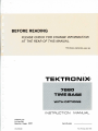
1
7B80 Instruction
TABLE OF CONTENTS
PAGE
PAGE
LIST OF ILLUSTRATIONS . . . . . . . . . . . . . . . . . . . iii
Trigger Slope . . . . . . . . . . . . . . . . . . . . 1-7
LIST OF TABLES . . . . . . . . . . . . . . . . . . . . . . . . . . iv
Trigger Level . . . . . . . . . . . . . . . . . . . . 1-7
SAFETY SUMMARY. . . . . . . . . . . . . . . . . . . . . . . . . v
Horizontal Sweep Rates . . . . . . . . . . . . . 1-7
Time Measurement . . . . . . . . . . . . . . . . 1-7
SECTION 1 OPERATING INSTRUCTIONS
Sweep Magnification . . . . . . . . . . . . . . . 1-7
INSTALLATION . . . . . . . . . . . . . . . . . . . 1-1
CONTROLS, CONNECTORS,
AND INDICATORS . . . . . . . . . . . . . . . . . . 1-1
FUNCTIONAL CHECK . . . . . . . . . . . . . . . 1-1
Variable Hold Off . . . . . . . . . . . . . . . . . 1-7
Mainframe Operating Modes . . . . . . . . . . 1-9
APPLICATIONS . . . . . . . . . . . . . . . . . . . . . . . .1-10
TIME-INTERVAL MEASUREMENTS . . . . .1-10
Setup Procedure . . . . . . . . . . . . . . . . . . 1-1
Period and Frequency Measurements . . . . .1-10
Sweep Functions . . . . . . . . . . . . . . . . . . 1-4
Rise-Time and Fall-Time Measurements . . .1-11
Triggering Functions . . . . . . . . . . . . . . . 1-4
Pulse Width Measurements . . . . . . . . . . . 1-12
GENERAL OPERATING INFORMATION . . 1-5
DELAYED-SWEEP MEASUREMENTS . . . . .1-12
Triggering Switch Logic . . . . . . . . . . . . . 1-5
X-Y PHASE MEASUREMENTS . . . . . . . . . .1-12
Triggering Modes . . . . . . . . . . . . . . . . . . 1-5
Trigger Coupling . . . . . . . . . . . . . . . . . . 1-6
Trigger Source . . . . . . . . . . . . . . . . . . . 1-6
SECTION 2 SPECIFICATION
STANDARD ACCESSORIES . . . . . . . . . . . 2-3
WARNING
THE REMAINING SECTIONS OF THIS MANUAL CONTAIN SERVICING
INSTRUCTIONS . THESE SERVICING INSTRUCTIONS
ARE FOR USE BY QUALIFIED PERSONNEL ONLY . T O AVOID
ELECTRICAL
SHOCK, DO
NOT PERFORM ANY SERVICING
OTHER THAN THAT CALLED OUT IN THE OPERATING INSTRUCTIONS UNLESS QUALIFIED TO DO SO.
71380 Instruction
TABLE
OF
CONTENTS
(CONT.)
PAGE
PAGE
SECTION 3 THEORY OF OPERATION
SOLDERING TECHNIQUES . . . . . . . . . . . . 4-9
BLOCK DIAGRAM DESCRIPTION . . . . . . . . . . . 3-1
DETAILED CIRCUIT DESCRIPTION . . . . . . . . . 3-1
LOGIC FUNDAMENTALS . . . . . . . . . . . . . 3-1
NON-DIGITAL DEVICES. . . . . . . . . . . . . . 3-2
FRONT-PANEL DISTRIBUTION O1 . . . . . 3-7
TRIGGER GENERATOR
O. . . . . . . . . .
3-7
LOGIC 03 . . . . . . . . . . . . . . . . . . . . . . . 3-9
SWEEP GENERATOR
4O . . . . . . . . . . . .3-11
TIME/DIVISION READOUT O5 .
. . . . . . .
3-14
INTERFACE CONNECTORS AND
POWER SUPPLY <~> . . . . . . . . . . . . . . .3-14
SECTION 4 MAINTENANCE
PREVENTIVE MAINTENANCE . . . . . . . . . . . . . 4-1
COMPONENT REMOVAL AND . . . . . . . .
REPLACEMENT. . . . . . . . . . . .
4-10
Circuit Boards . . . . . . . . . . . . . . . . . . . .4-10
Switches . . . . . . . . . . . . . . . . . . . . . . .4-12
Semiconductors . . . . . . . . . . . . . . . . . .4-12
Interconnecting Pins . . . . . . . . . . . . . . .4-13
Front-Panel Lights . . . . . . . . . . . . . . . . .4-16
ADJUSTMENT AFTER REPAIR . . . . . . . . .4-16
INSTRUMENT REPACKAGING . . . . . . . . .4-16
SECTION 5 PERFORMANCE CHECK AND
ADJUSTMENT
PRELIMINARY INFORMATION . . . . . . . . 5-1
TEST EQUIPMENT REQUIRED . . . . . . . . . 5-1
CLEANING . . . . . . . . . . . . . . . . . . . . . . . 4-1
INDEX TO PERFORMANCE CHECK
AND ADJUSTMENT PROCEDURE . . . . . . . 5-3
VISUAL INSPECTION . . . . . . . . . . . . . . . . 4-1
PRELIMINARY PROCEDURE . . . . . . . . . . 5-3
LUBRICATION . . . . . . . . . . . . . . . . . . . . 4-1
SEMICONDUCTOR CHECKS . . . . . . . . . . . 4-2
ADJUSTMENT AFTER REPAIR . . . . . . . . . 4-2
TROUBLESHOOTING. . . . . . . . . . . . . . . . . . . . 4-3
TROUBLESHOOTING AIDS . . . . . . . . . . . 4-3
TROUBLESHOOTING EQUIPMENT . . . . . . 4-5
TROUBLESHOOTING TECHNIQUES . . . . . 4-6
CORRECTIVE MAINTENANCE . . . . . . . . . . . . . 4-9
OBTAINING REPLACEMENT PARTS . . . . . 4-9
SECTION 6 REPLACEABLE ELECTRICAL PARTS
SECTION 7 INSTRUMENT OPTIONS
SECTION 8 DIAGRAMS AND CIRCUIT BOARD
ILLUSTRATIONS
SECTION 9 REPLACEABLE MECHANICAL PARTS
CHANGE INFORMATION
71380 Instruction
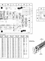
LIST OF ILLUSTRATIONS
FIGURE
NO .
1-1
1-2
1-3
1-4
1-5 1-6
1-7
1-8
2-1
3-1
3-2
3-3
3-4
3-5
3-6
4-1
4-2
4-3
4-4
PAGE
Frontispiece . . . . . . . . . . . . . . . . . . .
Location of release latch . . . . . . . . . . .
Front-panel controls, connectors,
and indicators . . . . . . . . . . . . . . . . . .
Effect of LEVEL control and SLOPE
switch on crt display . . . . . . . . . . . . .
Area of graticule used for most accurate
time measurements . . . . . . . . . . . . . .
Operation of sweep magnifier . . . . . . .
Measuring the period and determining
the frequency of a displayed waveform .
Measuring the rise time and fall time of
a displayed waveform . . . . . . . . . . . . .
Measuring the pulse width of a displayed
waveform . . . . . . . . . . . . . . . . . . . . .
71380 dimensional drawing . . . . . . . . .
Basic block diagram of the 71380
Time-Base Unit . . . . . . . . . . . . . . . . .
Detailed block diagram of Trigger
Generator . . . . . . . . . . . . . . . . . . . .
Functional diagram of Trigger Source
Selector . . . . . . . . . . . . . . . . . . . . . .
Timing diagram for Gate Generator
(Q92, Q96, Q98) . . . . . . . . . . . . . . . .
Detailed block diagram of Logic circuit .
Detailed block diagram of Sweep
Generator . . . . . . . . . . . . . . . . . . . .
Lubrication procedure for a typical
cam switch . . . . . . . . . . . . . . . . . . . .
Semiconductor lead configuration . . . .
Inter-board multi-pin connector
assembly . . . . . . . . . . . . . . . . . . . . .
End-lead multi-pin connector
assembly . . . . . . . . . . . . . . . . . . . . .
. . . vi
. . 1-1
. . 1-2
. . 1-8
. . 1-9
. . 1-9
. .1-10
. .1-11
. .1-12
. . 2-3
. . 3-2
. . 3-6
. . 3-8
. . 3-9
. . 3-10
. .3-12
. . 4-2
. . 4-4
. . 4-5
. . 4-5
FIGURE
NO .
4-5
4-6
4-7
4-8
4-9
4-10
4-11
4-12
PAGE
Location of pin numbers on Interface
connector . . . . . . . . . . . . . . . . . .
71380 troubleshooting chart . . . . . . .
Readout board removal procedure . .
Coaxial end-lead connector assembly .
Cam switch removal procedure. . . . .
Removal procedure for typical
push-button switch . . . . . . . . . . . .
Exploded view of circuit-board pin
and ferrule . . . . . . . . . . . . . . . . . .
Front-panel light socket assembly . . .
.
.
.
.
.
.
.
.
.
.
.
.
.
.
.
. 4-5
. 4-8
.4-11
.4-12
.4-14
. . . .4-15
. . . .4-16
. . . .4-16
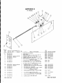
The illustrations in Section 8 are located near their associated Diagrams on the foldout pages .
8-1
8-2
8-3
8-4
8-5
8-6
8-7
8-8
8-9
8-10
8-11
8-12
8-13
8-14
8-15
8-16
Semiconductor lead configurations .
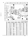
Location of circuit boards in the 7880 .
A1-Interface circuit board assembly .
A2-Trigger circuit board assembly .
A3-Readout circuit board assembly .
A1-Interface circuit board assembly .
A2-Trigger circuit board assembly .
A1-Interface circuit board assembly .
A1-Interface circuit board assembly .
A3-Readout circuit board assembly .
A1-Interface circuit board assembly .
A3-Readout circuit board assembly .
A1-Interface circuit board assembly .
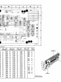
A5-X-Y Switch circuit board assembly .
Location of Sweep Timing adjustments .
Location of Triggering adjustments .
71380 Instruction
LIST OF TABLES
TABLE
NO .
PAGE
TABLE
NO .
PAGE
2-1
Electrical Characteristics . . . . . . . . . . . . . 2-1
3-2
Readout Character Selection . . . . . . . . . .3.15
2-2
Environmental Characteristics . . . . . . . . . 2-3
5-1
Test Equipment . . . . . . . . . . . . . . . . . . 5-2
2-3
Physical Characteristics . . . . . . . . . . . . . . 2-3
5-2
Sweep Timing . . . . . . . . . . . . . . . . . . . . 5-10
3-1
Basic Logic Reference . . . . . . . . . . . . . . 3-3
5-3
Magnified Sweep Timing . . . . . . . . . . . . . 5-11
71380 Instruction
SAFETY SUMMARY
This manual contains safety information which the user must follow to ensure safe operation of this instrument . WARNING
information is intended to protect the operator ; CAUTION information is intended to protect the instrument . The following
are general safety precautions that must be observed during all phases of operation and maintenance .
WARNING
Ground the Instrument
To reduce electrical-shock hazard, the mainframe (oscilloscope) chassis must be properly grounded. Refer to the mainframe
manual for grounding information .
Do Not Operate in Explosive Atmosphere
Do not operate this instrument in an area where flammable gases or fumes are present. Such operation could cause an
explosion .
Avoid Live Circuits
Electrical-shock hazards are present in this instrument. The protective instrument covers must not be removed by operating
personnel. Component replacement and internal adjustments must be referred to qualified service personnel.
Do Not Service or Adjust Alone
Do not service or make internal adjustments to this instrument unless another person, capable of giving first aid and resuscitation, is present.
WARNING
Warning Statements
Warning statements accompany potentially dangerous procedures in this manual . The following warnings appear in this
manual and are listed here for additional emphasis .
To avoid electrical shock, disconnect the instrument from the power source before soldering.
To avoid electrical shock, disconnect the instrument from the power source before replacing components.
Handle silicone grease with care . Avoid getting silicone grease in eyes. Wash hands thoroughly after use.
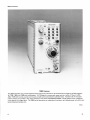
71380 Features
The 7880 Time-Base unit provides calibrated sweep rates from 5 seconds to 10 nanoseconds and triggering to 400 megahertz
for 7700-, 7800-, and 7900-series oscilloscopes . A X10 Magnifier increases each sweep rate by a factor of 10 and a VARIABLE TIME/DIV control provides continuously variable sweep rates between calibrated steps . Variable hold off and alphanumeric readout are provided . Also, when operating in the AUTO TRIGGERING MODE, a bright baseline trace is displayed
in the absence of a trigger signal . The 71380 can be operated as an independent time base or as a delayed-sweep unit with a companion delaying time-base unit .
1958-1
Section 1-71380
OPERATING INSTRUCTIONS
The 71380 Time-Base unit operates with a Tektronix 7700-, 7800-, and 7900-series oscilloscope mainframes and a 7A-series
amplifier unit to form a complete oscilloscope system . This section describes the operation of the front-panel controls and
connectors, provides general operating information, a functional check procedure, and basic applications for this instrument .
INSTALLATION
The time-base unit is designed to operate in the horizontal
plug-in compartment of the mainframe. This instrument
can also be installed in a vertical plug-in compartment to
provide a vertical sweep on the crt. However, when used in
this manner, there are no internal triggering or retrace
blanking provisions, and the unit may not meet the specifications given in Section 2.
To install the unit in a plug-in compartment, push it in until
it fits firmly into the compartment. The front panel of the
unit should be flush with the front panel of the mainframe .
Even though the gain of the mainframe is standardized, the
sweep calibration of the unit should be checked when installed . The procedure for checking the unit is given under
Sweep Functions in the Functional Check procedure in this
section .
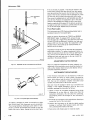
To remove the unit, pull the release latch (see Figure 1-1)
to disengage the unit from the mainframe, and pull it out of
the plug-in compartment.
2. Install an amplifier plug-in unit in a vertical compartment .
3. Set the time-base unit controls as follows :
SLOPE
MODE
COUPLING
SOURCE
POSITION
TIME/DIV
VARIABLE
(CAL IN)
HOLD OFF
MAG
(+)
P-P AUTO
AC
INT
Midrange
1 ms
Calibrated (Pushed in)
MIN (fully counterclockwise)
X1 (pushed in)
4. Turn on the mainframe and allow at least 20 minutes
warmup .
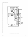
CONTROLS, CONNECTORS, AND INDICATORS
All controls, connectors, and indicators required for the
operation of the time-base unit are located on the front
panel . Figure 1-2 shows and provides a brief description of
all front-panel controls, connectors, and indicators . More
detailed information is given in the General Operating
I nstructions .
FUNCTIONAL CHECK
The following procedures are provided for checking basic
instrument functions. Refer to the description of the controls, connectors, and indicators while performing this procedure . If performing the functional check procedure
reveals a malfunction or possible improper adjustment, first
check the operation of the associated plug-in units, then refer to the instruction manual for maintenance and adjustment procedures .
Setup Procedure
1 . Install the time-base unit being checked in the A horizontal compartment of the mainframe.
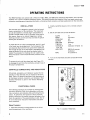
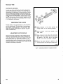
RELEASE
LATCH
Fig. 1-1 . Location of release latch .
1958-3
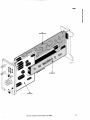
Fig. 1-2. Front-panel controls, connectors, and indicators.
Operating Instructions-7B80
TRIGGERING
LEVEL Control-Selects a point on the trigger signal where triggering occurs .
SLOPE Switch-Permits sweep to be triggered on negative or positive-going portions of the trigger signal .
READY Indicator-Illuminates when sweep circuit is armed (SINGLE SWEEP Mode) .
TRIG'D Indicator-Illuminates when the display is triggered .
MODE Pushbuttons-Selects the operating mode of the triggering circuit .
COUPLING Pushbuttons-Selects the method of coupling the trigger signal to triggering circuit.
SOURCE Pushbuttons-Selects source of the trigger signal .
SWEEP
POSITION Control-Provides horizontal positioning.
FINE Control-Provides precise horizontal positioning.
MAG Pushbutton-Selects magnified X10 or unmagnified sweep.
HOLD OFF Control-Permits hold off period to be varied to improve trigger stability on repetitive complex waveforms.
TIME/DIV Selector-Selects the sweep rate of the sweep generator.
VARIABLE Control and CAL Switch-Selects calibrated or uncalibrated sweep rates. Uncalibrated sweep rates can
be continuously reduced to at least the sweep rate of the next slower position .
SWP CAL Adjustment-Compensates for basic timing changes due to the differences in sensitivity of mainframes
EXTERNAL TRIGGER INPUT
EXT TRIG ATTENUATOR-Selects attenuation factor for external trigger signals .
EXT TRIG IN Connector-Connector (BNC type) provides input for external trigger signals.
1958-4
Fig. 1-2. Front-panel controls, connectors, and indicators (coat.) .
Operating Instructions-71380
5. Set the mainframe vertical and horizontal modes to display the plug-in units used and adjust the intensity and
focus for a well-defined display . See the oscilloscope mainframe and amplifier unit instruction manuals for detailed
operating instructions .
Sweep Functions
NORMAL SWEEP. Perform the following procedure to obtain a normal sweep and to demonstrate the function of the
related controls :
1 . Perform the preceding Setup Procedure.
2. Connect a 0.4-volt, 1-kilohertz signal from the mainframe calibrator to the amplifier unit input.
3. Set the amplifier unit deflection factor for 4 divisions of
display.
4. Adjust the LEVEL control for a stable display .
5 . Turn the POSITION control and note that the trace
moves horizontally .
6. Turn the FINE control and note that the display can be
precisely positioned horizontally .
7. Check the display for one complete cycle per division . If
necessary, adjust the front-panel SWP CAL screwdriver adjustment for one complete cycle per division over the
center 8 graticule divisions. Be sure that the timing of the
mainframe calibrator signal is accurate to within 0.25%
(+20 to +30° C) .
8. Press to release the VARIABLE (CAL IN) control . Turn
the VARIABLE (CAL IN) control fully counterclockwise
and note that the displayed sweep rate changes to at least
the next slower TIME/DIV switch setting (i .e ., 2 milliseconds/division) . Press the VARIABLE (CAL IN) knob in
to the calibrated position .
MAGNIFIED SWEEP. Perform the following procedure to
obtain a X10 magnified display and to demonstrate the
function of the related controls :
1 . Obtain a one cycle per division display as described in
the preceding Normal Sweep procedure .
2. Press to release the MAG button (X10). Note that the
unmagnified display within the center division of the graticule is magnified to about 10 divisions.
3. Press the MAG button (X1) .
Triggering Functions
Perform the following procedure to obtain a triggered
sweep and to demonstrate the functions of the related
controls :
1 . Obtain a display as described in the preceding Normal
Sweep procedure.
2. Press the AUTO MODE button and turn the LEVEL
control fully counterclockwise to obtain a free-running
sweep.
3. Slowly turn the HOLD OFF control clockwise and note
that a stable display can be obtained at several positions of
the HOLD OFF control. Return the HOLD OFF control to
the fully counterclockwise (MIN) position .
NOTE
The HOLD OFF control varies the sweep hold-off
time which effectively changes the repetition-rate
of the horizontal sweep signal. However, its primary function is to obtain a stable display of
complex waveforms which are otherwise difficult
to trigger.
4. Press the AC, AC HF REJ, and DC COUPLING buttons
for both the + and - positions of the SLOPE switch and
check for a stable display (LEVEL control may be adjusted,
if necessary, to obtain a stable display) .
5. Apply the 0.4-volt, 1 kilohertz signal from the mainframe calibrator to the amplifier unit and to the EXT TR IG
IN connector.
6. Press the EXT SOURCE button and set the amplifier
unit deflection factor for a 4-division display.
7. Press the AC, AC HF REJ, and DC COUPLING buttons
for both the + and - positions of the SLOPE switch and
check for a stable display (LEVEL control may be adjusted,
if necessary, for a stable display) .
Operating Instructions-71380
8 . Press the AC COUPLING, INT SOURCE, and NORM
MODE buttons . Adjust the LEVEL control for a stable
display .
9 . Press the AUTO MODE button and adjust the LEVEL
control for a free-running display .
10 . Press the NORM MODE button and check for no
display .
11 . Adjust the LEVEL control for a stable display and
press the SINGLE SWP MODE button .
12 . Note that one trace occurs when the RESET MODE
button is pressed .
13 . Disconnect the mainframe calibrator signal from the
amplifier unit input and press the RESET MODE button .
Check for no display and note that the READY indicator
is lit .
14 . Note that one trace occurs and that the READY indicator extinguishes when the mainframe calibrator signal is
reconnected to the amplifier unit input .
GENERAL OPERATING INFORMATION
Triggering Switch Logic
The MODE, COUPLING, and SOURCE push buttons of the
TRIGGERING switches are arranged in a sequence which
places the most-often used position at the top of each series
of push buttons . With this arrangement, a stable display can
usually be obtained by pressing the top push buttons : P-P
AUTO, AC, INT. When an adequate trigger signal is applied
and the LEVEL control is correctly set, the unit is triggered
as indicated by the illuminated TRIG'D light . If the
TRIG'D light is not on, the LEVEL control is either at a
setting outside the range of the trigger signal applied to this
unit from the vertical unit, the trigger signal amplitude is inadequate, or its frequency is below the lower frequency
limit of the AC COUPLING switch position . If the desired
display is not obtained with these buttons pushed in, other
selections must be made . Refer to the following discussions
or the instruction manuals for the associated oscilloscope
mainframe and vertical unit(s) for more information .
Triggering Modes
The MODE push-button switches select the mode in which
the sweep is triggered .
P-P AUTO . The P-P AUTO MODE provides a triggered display at any setting of the LEVEL control whenever an adequate trigger signal is applied . The range of the LEVEL
control in the P-P AUTO MODE is between approximately
10% and 90% of the peak-to-peak amplitude of the trigger
signal . The LEVEL control can be set so that the displayed
waveform starts at any point within this range on either
slope . The trigger circuits automatically compensate for a
change in trigger-signal amplitude . Therefore, if the LEVEL
control is set to start the waveform display at a certain percentage point on the leading edge of a low-amplitude signal,
it triggers at the same percentage point on the leading edge
of a high-amplitude signal if the LEVEL control is not
changed . When the trigger repetition rate is outside the
parameter given in the Specification section, or when the
trigger signal is inadequate, the sweep free runs at the rate
indicated by the TIME/DIV switch to produce a bright
base-line reference trace (TRIG'D light off) . When an adequate trigger signal is again applied, the free-running condition ends and a triggered display is presented .
The P-P AUTO MODE is particularly useful when observing
a series of waveforms, since it is not necessary to reset the
LEVEL control for each observation . The P-P AUTO
MODE is used for most applications because of the ease of
obtaining a triggered display . The AUTO, NORM, and
SINGLE-SWP MODE settings may be used for special
applications .
AUTO . The AUTO MODE provides a triggered display
with the correct setting of the LEVEL control whenever an
adequate trigger signal is applied (see Trigger Level discussions) . The TRIG'D light indicates when the display is
triggered .
When the trigger repetition rate is outside the frequency
range selected by the COUPLING switch or the trigger signal is inadequate, the sweep free runs at the rate indicated
by the TIME/DIV switch (TRIG'D indicator off) . An adequate trigger signal ends the free-running condition and a
triggered display is presented . The sweep also free runs at
the rate indicated by the TIME/DIV switch when the
LEVEL control is at a setting outside the amplitude range
of the trigger signal . This type of free-running display is
useful when it is desired to measure only the peak-to-peak
amplitude of a signal without observing the waveshape
(such as bandwidth measurements) .
NORMAL . The NORM MODE provides a triggered display
with the correct setting of the LEVEL control whenever an
adequate trigger signal is applied . The TRIG'D light indicates when the display is triggered .
Operating Instructions-71380
The normal trigger mode must be used to produce triggered
displays with trigger repetition rates below about 30 hertz.
When the TRIG'D light is off, no trace is displayed.
SINGLE SWEEP. When the signal to be displayed is not repetitive or varies in amplitude, waveshape, or repetition
rate, a conventional repetitive type display may produce an
unstable presentation . Under these circumstances, a stable
display can often be obtained by using the single-sweep
feature of this unit . The single-sweep mode is also useful to
photograph non-repetitive or unstable displays .
To obtain a single-sweep display of a repetitive signal, first
obtain the best possible display in the NORM MODE . Then,
without changing the other TRIGGERING controls, press
the SINGLE SWP RESET button . A single trace is presented each time this button is pressed. Further sweeps cannot
be presented until the SINGLE SWP RESET button is pressed again. If the displayed signal is a complex waveform
composed of varying amplitude pulses, successive singlesweep displays may not start at the same point on the waveform . To avoid confusion due to the crt persistence, allow
the display to disappear before pressing the SINGLE SWP
RESET button again. At fast sweep rates, it may be difficult to view the single-sweep display . The apparent trace
intensity can be increased by reducing the ambient light
level or by using a viewing hood as recommended in the
mainframe instruction manual .
When using the single-sweep mode to photograph waveforms, the graticule may have to be photographed
separately in the normal manner to prevent over exposing
the film . Be sure the camera system is well protected
against stray light, or operate the system in a darkened
room . For repetitive waveforms, press the SINGLE SWP
RESET button only once for each waveform unless the signal is completely symmetrical . Otherwise, multiple waveforms may appear on the film . For random signals, the lens
can be left open until the signal triggers the unit . Further
information on photographic techniques is given in the
appropriate camera instruction manual .
Trigger Coupling
The TRIGGERING COUPLING push buttons select the
method in which the trigger signal is connected to the trigger circuits . Each position permits selection or rejection of
some frequency components of the signal which triggers
the sweep .
AC . AC COUPLING blocks the do component of the trigger signal . Signals with low-frequency components below
about 30 hertz are attenuated . In general, AC COUPLING
can be used for most applications . However, if the signal
contains unwanted frequency components or if the sweep is
to be triggered at a low repetition rate or do level, one of
the other COUPLING switch positions will provide a better
display.
AC LF REJ. AC LF REJ COUPLING rejects dc, and attenuates low-frequency trigger signals below about 30 kilohertz. Therefore, the sweep is triggered only by the higherfrequency components of the trigger signal . This position is
particularly useful for providing stable triggering if the trigger signal contains line-frequency components . Also, the
AC LF REJ position provides the best alternate-mode vertical displays at fast sweep rates when comparing two or
more unrelated signals.
AC HF REJ. AC HF REJ COUPLING passes all lowfrequency signals between about 30 hertz and 50 kilohertz.
Dc is rejected and signals outside the above range are attenuated . When triggering from complex waveforms, this position is useful to provide a stable display of the lowfrequency components .
DC . DC COUPLING can be used to provide stable triggering from low-frequency signals which would be attenuated
in the other COUPLING switch positions. DC COUPLING
can be used to trigger the sweep when the trigger signal
reaches a do level set by the LEVEL control. When using
internal triggering, the setting of the vertical unit position
control affects the triggering point.
Trigger Source
The TRIGGERING SOURCE push buttons select the
source of the trigger signal which is connected to the trigger
circuits .
INTERNAL . The INT position connects the trigger signal
from the vertical plug-in unit . Further selection of the internal trigger signal may be provided by the vertical plug-in
unit or by the mainframe; see the instruction manuals for
these instruments for more information . For most applications, the internal source can be used . However, some
applications require special triggering which cannot be obtained in the INT positicn . In such cases, the LINE or EXT
positions of the SOURCE switches must be used .
LINE . The LINE position connects a sample of the powerline voltage from the mainframe to the trigger circuit. Line
triggering is useful when the input signal is time-related
(multiple or submultiple) to the line frequency. It is also
useful for providing a stable display of a line-frequency
component in a complex waveform .
Operating Instructions-71380
EXTERNAL . The EXT position connects the signal from
the EXT TRIG IN connector to the trigger circuit. The external signal must be time-related to the displayed waveform for a stable display. An external trigger signal can be
used to provide a triggered display when the internal signal
is either too low in amplitude for correct triggering or contains signal components on which triggering is not desired.
It is also useful when signal tracing in amplifiers, phase-shift
networks, wave-shaping circuits, etc. The signal from a
single point in the circuit can be connected to the EXT
TRIG IN connector through a probe or cable. The sweep is
then triggered by the same signal at all times and allows amplitude, time relationship, or waveshape changes of signals
at various points in the circuit to be examined without resetting the TRIGGERING controls .
sequence . The VARIABLE TIME/DIV control must be in
the calibrated position and the MAG switch set to X1 to
obtain the sweep rate indicated by the TIME/DIV switch .
However, the mainframe crt readout will display the appropriate sweep rate .
The VARIABLE TIME/DIV control includes a two-position
switch to determine if the sweep rate is calibrated, or uncalibrated . When the VARIABLE control is pressed in, it is
inoperative and the sweep rate is calibrated . When pressed
and released outward, the VARIABLE control is activated
for uncalibrated sweep rates, to at least the sweep rate of
the next slower position .
The =10 push button attenuates the external trigger signal
by a factor of 10 . Attenuation of high amplitude external
trigger signals is desirable to increase the effective range of
the LEVEL control.
A calibrated sweep rate can be obtained in any position of
the VARIABLE control by pressing in the VARIABLE control . This feature is particularly useful when a specific uncalibrated sweep rate has been obtained and it is desired to
switch between calibrated and uncalibrated displays .
Trigger Slope
Time Measurement
The TRIGGERING SLOPE switch (concentric with the
TRIGGERING LEVEL control) determines whether the
trigger circuit responds on the positive- or negative-going
portion of the trigger signal . When the SLOPE switch is in
the (+) (positive-going) position, the display starts or. the
positive-going portion of the waveform (see Figure 1-3) .
When several cycles of a signal appear in the display, the
setting of the SLOPE switch is often unimportant. However, if only a certain portion of a cycle is to be displayed,
correct setting of the SLOPE switch is important to provide
a display that starts on the desired slope of the input signal .
Trigger Level
The TRIGGERING LEVEL control determines the voltage
level on the trigger signal at which the sweep is triggered.
When the LEVEL control is set in the + region, the trigger
circuit responds at a more positive point on the trigger signal. When the LEVEL control is set in the - region, the
trigger circuit responds at a more negative point on the
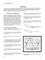
trigger signal . Figure 1-3 illustrates this effect with different
settings of the SLOPE switch .
To set the LEVEL control, first select the TRIGGERING
MODE, COUPLING, SOURCE, and SLOPE . Then set the
LEVEL control fully counterclockwise and rotate it clockwise until the display starts at the desired point.
Horizontal Sweep Rates
The TIME/DIV switch provides calibrated sweep rates from
5 seconds/division to 10 nanoseconds/division in a 1-2-5
When making time measurements from the graticule, the
area between the second and tenth vertical lines of the graticule provides the most linear time measurements (see
Figure 1-4) . Position the start of the timing area to the
second vertical line and adjust the TIME/DIV switch so the
end of the timing area falls between the second and tenth
vertical lines.
Sweep Magnification
The sweep magnifier can be used to expand the display by a
factor of 10 . The center division of the unmagnified display
is the portion visible on the crt in the magnified form (see
Figure 1-5) . The equivalent length of the magnified sweep is
more than 100 divisions ; any 10 division portion can be
viewed by adjusting the POSITION and FINE POSITION
controls to bring the desired portion into the viewing area.
When the MAG switch is set to X10 (OUT) the equivalent
magnified sweep rate can be determined by dividing the
TIME/DIV setting by 10 ; the equivalent magnified sweep
rate is displayed on the crt readout.
Variable Hold Off
The HOLD OFF control improves triggering stability on repetitive complex waveforms by effectively changing the
repetition rate of the horizontal sweep signal . The HOLD
OFF control should normally be set to its minimum setting.
When a stable display cannot be obtained with the TRIGGERING LEVEL control, the HOLD OFF control can be
varied for an improved display . If a stable display cannot be
obtained at any setting of the LEVEL and HOLD OFF controls, check the TRIGGERING COUPLING and SOURCE
switch settings .
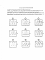
Fig . 1-3 . Effect of LEVEL control and SLOPE switch on crt display .
Mainframe Operating Modes
The time-base unit can be operated either as an independent time base in any Tektronix 7700-, 7800-, or 7900series oscilloscope mainframe, or as a delayed-sweep unit in
those mainframes that have two horizontal compartments .
A companion delaying time-base unit is required for delayedsweep operation. Refer to the delaying time-base unit instruction manual for additional information .
Fig. 1-4. Area of graticule used for most accurate time measurements.
Fig. 1-5. Operation of sweep magnifier.
Operating Instructions-71380
APPLICATIONS
The following information describes procedures and techniques for making basic time measurements with the time-base unit
installed in a Tektronix 7700-, 7800-, or 7900-series oscilloscope . These procedures provide enough detail to enable the
operator to adapt them to other related time measurements . Contact your Tektronix Field Office or representative for
assistance in making measurements that are not described in this manual .
TIME-INTERVAL MEASUREMENTS
Since time is a function of the sweep rate and the horizontal distance (in divisions) that the sweep travels across the
graticule in a calibrated-sweep oscilloscope system, the time
interval between any two points on a waveform can be
accurately measured . The following procedures provide
methods to measure some of the more common timerelated definable characteristics of a waveform such as
period, frequency, rise time, fall time, and pulse width . The
procedure for each of these measurements is essentially the
same, except for the points between which the measurements are made . The time interval between any two
selected points on a displayed waveform can be measured
with basically the same technique .
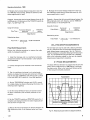
7. Measure the horizontal distance in divisions over 1 complete cycle of the displayed waveform (see Figure 1-6) .
8. Multiply the horizontal distance measured in Step 7 by
the TIME/DIV switch setting . (Divide the answer by 10 if
sweep magnification is used .)
Example : Assume that the horizontal distance over 1 complete cycle is 7 divisions, and the TIME/DIV switch setting
is .1 ms (see Figure 1-6) .
Using the formula :
Period = Horizontal distance X TIME/DIV setting
Magnification
Period and Frequency Measurements
Perform the following procedure to measure the period and
determine the frequency of a displayed waveform :
Substituting values :
Period = 7 X 0.1 ms
1
1 . Install the time-base unit in a mainframe horizontal
compartment (either A or B horizontal in a four-compartment mainframe) .
2 . Connect the signal to be measured to the vertical unit
input.
3. Set the mainframe horizontal- and vertical-mode switches to display the time base and vertical units. (Check that
the time base VARIABLE (CAL IN) control is pushed in
and the HOLD OFF control is in the MIN position .)
4. Set the TRIGGERING switches and LEVEL control for
a stable display (see General Operating Information for
selecting proper triggering) .
5. Set the vertical deflection factor and position control
for about a 5-division display, vertically centered on the
graticule .
6. Set the TIME/DIV switch and POSITION control for 1
complete cycle displayed within the center 8 graticule divisions as shown in Figure 1-6.
1- 1 0
=
0.7 millisecond
1
FREQUENCY = PERIOD
MENEM
. . . ENEEMENEW
100MILWEENtWO
-0
4ONGNNNONNNIN M
WANNEWNSONFAN
HMMMMMMEMM
NEE MOORE
100
90
10
MEASURE HORIZONTAL DISTANCE FROM
ATOB
1985-10
Fig. 1-6. Measuring the period and determining the frequency of a
displayed waveform.
Operating Instructions-71380
9 . Determine the frequency of the displayed waveform obtained in steps 1 through 8 by taking the reciprocal of the
period of 1 cycle .
RISE TIME
Example : Assume that the period of the displayed waveform is 0 .7 millisecond .
AMIMEM
NEENN mm~
W"
o ~1
Using the formula :
Frequency
=
1
Period
I~ICPIP
Substituting values :
Frequency =
1
0 .7 ms
1I
=
MEASURE HORIZONTAL DISTANCE FROM
A TO B (10% TO 90%)
1 .43 kilohertz
FALL TIME
Egg ME
1
E MEN
E
fttWaONE
q
MMUNNIN
Em
Rise-Time and Fall-Time Measurements
Perform the following procedure to measure the rise time
and fall time of a displayed waveform :
WITIM
M
a
1 . Install the time-base unit in a mainframe horizontal
compartment (either A or B horizontal in a four-compartment mainframe) .
2 . Connect the signal to be measured to the vertical unit
input .
3 . Set the mainframe horizontal- and vertical-mode switches to display the time base and the vertical unit . (Check
that the time base VARIABLE (CAL IN) control is pushed
in and the HOLD OFF control is in the MIN position .)
4 . Set the TRIGGERING switches and LEVEL control for
a stable display (see General Operating Information for
selecting proper triggering) .
5 . Set the vertical deflection factor and position control
for a vertically-centered display with an exact number of
divisions of amplitude .
6 . Set the TIME/DIV switch and POSITION control to display the rising or falling portion of the waveform within the
center 8 graticule divisions as shown in Figure 1-7 (see
General Operating Information in this section for discussion
of timing measurement accuracy) .
7 . Determine rise time or fall time by measuring the horizontal distance in divisions between the point on the rising
0
p. . .
. .
. .
MEASURE HORIZONTAL DISTANCE FROM
A TO B (90% TO 10%)
1985-11 A
Fig . 1-7 . Measuring the rise time and fall time of a displayed waveform .
or falling portion of the waveform that is 10% and the
point that is 90% of the total display amplitude (see . Figure
1-7) .
NOTE
The left edge of the oscilloscope graticule is
scribed with 0, 10, 90, and 100% lines for convenience when measuring rise time or fall time.
To use this feature, adjust the vertical deflection
factor and position control to fit the display between the 0 and 100% graticule lines. Then
measure the horizontal distance between the
points where the waveform crosses the 10% and
90% graticule lines.
Operating Instructions-71380
8. Multiply the horizontal distance measured in step 7 by
the TIME/DIV switch setting. (Divide the answer by 10 if
sweep magnification is used .)
8. Multiply the horizonal distance measured in step 7 by
the TIME/DIV switch setting. (Divide the answer by 10 if
sweep magnification is used .)
Example: Assume that the horizontal distance from the 10
to 90% points is 2.5 divisions and the TIME/DIV switch setting is .1 p.s (see Figure 1-7) .
Example : Assume that the horizontal distance between the
50% amplitude points is 3 divisions, and the TIME/DIV
switch setting is .1 ms (see Figure 1-8) .
Using the formula :
Using the formula :
Horizontal distance
Rise Time =
(divisions)
X
Pulse Width =
TIME/DIV
setting
Magnification
Substituting values :
Substituting values :
Pulse Width = 3 X 0.1 ms = 0.3 millisecond
1
1
Perform the following procedure to measure the pulse
width of a displayed waveform :
1 . Install the time-base unit in a mainframe horizontal
compartment (either A or B horizontal in a four-compartment mainframe) .
2. Connect the signal to be measured to the vertical unit
input.
DELAYED-SWEEP MEASUREMENTS
The time-base unit may be used with a delaying time-base
unit in a mainframe with two horizontal compartments to
make delayed-sweep measurements . See the Tektronix
Products Catalog for compatible delaying time-base plug-in
units. If a compatible delaying time-base unit is available,
refer to the instruction manual for that unit for detailed
delayed-sweep measurement procedures .
X-Y PHASE MEASUREMENTS
The phase difference between two signals with the same frequency can be measured with a 71380 Option 2 and amplifier plug-in units. Refer to the Instrument Options section
of this manual for detailed procedures .
3. Set the mainframe horizontal- and vertical-mode
switches to display the time base and vertical unit . (Check
that the time base VARIABLE (CAL IN) control is pushed
in and the HOLD OFF control is in the MIN position .)
4. Set the TRIGGERING switches and LEVEL control
for a stable display (see General Operating Information for
selecting proper triggering) .
PULSE WIDTH
io
90
A
5. Set the vertical deflection factor and position control
for about a 5-division pulse vertically centered on the
graticule .
6. Set the TIME/DIV switch and POSITION control for 1
complete pulse displayed within the center 8 graticule divisions as shown in Figure 1-8.
7. Measure the horizontal distance in divisions between the
50% amplitude points of the displayed pulse (see Figure
1-8) .
1- 1 2
TIME/DIV
setting
X
Magnification
Rise Time = 2.5 x 0.1 ps = 0.25 microsecond
Pulse Width Measurements
Horizontal
distance
B
I
I
I
1
0
. .I . . . .
I
I
.
. .I .
..
MEASURE HORIZONTAL DISTANCE FROM
A TO B
1985-12
Fig. 1-8. Measuring the pulse width of a displayed waveform .
Section 2-71380
SPECIFICATION
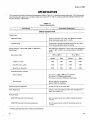
This instrument will meet the electrical characteristics listed in Table 2-1, following complete adjustment. The following electrical characteristics apply over an ambient temperature range of 0° to +50° C, except as otherwise indicated . Warmup time
for given accuracy is 20 minutes.
TABLE 2-1
Electrical Characteristics
Performance Requirement
Characteristic
SWEEP GENERATOR
Sweep Rates
Calibrated Range
5 s/div to 10 ns/div in 27 steps. X10 Magnifier extends
fastest calibrated sweep rate to 1 ns/div .
Variable Range
Continuously variable uncalibrated sweep rate to at least
2.5 times the calibrated sweep rate setting.
Sweep Accuracy' (With 7700, 7800, or 7900-Series
Mainframes)
Over Center 8 Div
With SWP CAL adjusted at 1 ms/div within the temperature
range of +20° to +30° C to a timing reference of 0.25% or
better .
0° to +50° C
+15° to +35° C
Unmag
Mag
Unmag
Mag
5 s/Div to 1 s/Div
4.0%
5.0%
5.0%
6.0%
0.5 s/Div to 0.1 ,its/Div
1 .5%
2.5%
2.5%
3.5%
50 ns/Div to 10 ns/Div
2.5%
4.0%
3.5%
5.0%
Excluded Portions of Sweep
Start of Sweep
First 10 ns in 7800, 7900-series mainframes .
First 20 ns in 7700-series mainframes .
First 50 ns in all other 7000-series mainframes.
End of Sweep
Beyond 10th div unmagnified .
Beyond 100th div magnified.
Sweep Length (Unmagnified)
At least 10 .2 div at all sweep rates.
MAG Registration
0.5 div or less from graticule center when changing from
MAG X10 to MAG X1 .
Position Range
POSITION Controls Fully Clockwise
Start of sweep must be to the right of graticule center at
1 ms/div .
POSITION Controls Fully Counterclockwise
End of sweep must be to the left of graticule center at
1 ms/div .
'The fastest calibrated sweep rate is limited by some mainframes.
Specification-71380
TABLE 2-1 (CONT.)
Electrical Characteristics
Performance Requirement
Characteristic
Trigger Holdoff Time
Minimum Holdoff Setting
5 s/Div to 1 ps/Div
2 times TIME/DIV setting or less .
0.5 ps/Div to 10 ns/Div
2.0 ps or less .
Extends holdoff time through at least 2 sweep lengths for
sweep rates of 20 ms/div or faster .
Variable Holdoff Range
TRIGGERING
Triggering Sensitivity from Repetitive Signal (Auto,
Norm and Single Sweep Modes)
Triggering Frequency
Range2
Coupling
Minimum Triggering
Signal Required
Internal
External
AC
30 Hz to50MHz
50 MHz to 400 MHz
0 .3 div
1 .5 div
50 mV
250 mV
AC LF REJ3
30 kHz to 50 MHz
50 MHz to 400 MHz
0.3 div
1 .5 div
50 mV
250 mV
AC HF REJ
30 Hz to50kHz
0.3 div
50 mV
Dc to 50 MHz
50 MHz to 400 MHz
0.3 div
1 .5 div
50 mV
250 mV
DC4
Internal Trigger Jitter
0.1 ns or less at 400 MHz.
External Trigger Input
Maximum Input Voltage
250 V (dc plus peak ac).
Input R and C
1 ME2 within 5%, 20 pF within 10%.
Level Range (Excluding P-P AUTO)
(Checked on 1 kHz sine wave .)
EXT - 1
At least + and -1 .5 volts.
EXT= 10
At least + and -15 volts.
P-P AUTO Operation Sensitivity (Ac or Dc Coupling)
Low Frequency Response
Triggering Frequency
Range
Minimum Triggering
Signal Required
Internal
External
200 Hz to 50 MHz
0.5 div
125 mV
50 MHz to 400 MHz
1 .5 div
375 mV
At least 50 Hz
2.0 div
500 mV
'The triggering frequency ranges given here are limited to the -3 dB frequency of the oscilloscope vertical system (mainframe and amplifier
unit) when operating from an internal source .
3 Will not trigger on sine waves at or below 60 Hz when amplitudes are less than 8 divisions internal or 3 volts external .
'The Triggering Frequency Range for DC COUPLING applies to frequencies above 30 Hz when operating in the AUTO TRIGGERING MODE .
2-2
Specification-7880
TABLE 2-2
Environmental Characteristics
Refer to the Specification section of the associated mainframe
manual .
TABLE 2-3
Physical Characteristics
Net Weight
Approximately 2 .1 pounds (1 kilogram).
Dimensions
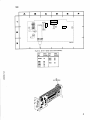
See Figure 2-1, dimensional drawing .
OVERALL DIMENSIONS
(MEASURED AT MAXIMUM POINTS)
aoo
ooa
nao
Do-
0
5.0
(12.7)
O
00
(3.0) 1
12 .5
(31 .7)
1 .2
NOTE :
.8
(2 .2)
14.5
(36 .9)
TOP FIGURES IN INCHES
LOWER FIGURES IN CENTIMETERS
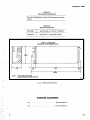
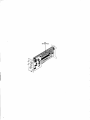
Fig . 2-1 . 7B80 dimensional drawing.
STANDARD ACCESSORIES
1 ea . . . . . . . . . . . . . . . . . . . . . . . . . . . . . Operators Manual
1 ea . . . . . . . . . . . . . . . . . . . . . . . . . . . . Instruction Manual
1958-5
Section 3-71380
THEORY OF OPERATION
This section of the manual describes the circuitry used in the 7880 Time-Base unit . The description begins with a discussion
of the instrument, using the block diagram shown in Figure 3-1 . Next, each circuit is described in detail with a block diagram
provided to show the major interconnections between circuits, and the relationship of the front-panel controls to each circuit.
Detailed schematic diagrams of each circuit are located in the diagrams foldout section at the back of this manual . Refer to
these diagrams throughout the following discussions for specific electrical values and relationships.
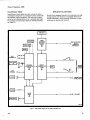
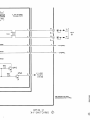
BLOCK DIAGRAM DESCRIPTION
The following discussion is provided to aid in understanding the overall concept of the time-base unit before the individual
circuits are discussed in detail . A basic block diagram is shown in Figure 3-1 . The numbered diamond in each block refers to
the corresponding circuit diagram at the rear of this manual .
TRIGGER GENERATOR
The Trigger Generator ensures a stable crt display by starting each sweep at the same point on the waveform . Circuitry is included for selection of trigger mode, coupling, and
source . The output of the Trigger Generator is a fast-rise
gate which enables the Sweep Generator.
SWEEP GENERATOR
The sweep sawtooth signal is initiated when the Trigger
Generator output is applied to the Sweep Generator . The
rate of change (slope) of the sawtooth signal is determined
by the TIME/DIV switch setting. The sawtooth signal provides horizontal deflection for the mainframe (oscilloscope) .
The Sweep Generator also generates a Sweep Gate pulse
which unblanks the crt in the mainframe.
LOGIC
The Logic circuits control the sweep modes and associated
functions of the time-base unit (e .g ., auto sweep, single
sweep, hold off, etc.) . The Logic circuits also generate the
control signals for the mainframe.
DETAILED CIRCUIT DESCRIPTION
The operation of circuits unique to this instrument is described in detail in this discussion . Circuits commonly used in the
electronics industry are not described in detail .
The following circuit analysis, with supporting illustrations, gives the names of individual stages, and shows how they are connected to form major circuits . These illustrations show the inputs and outputs for each circuit and the relationship of the
front-panel controls to the individual stages . The detailed circuit diagrams from which the illustrations are derived are shown
in the diagrams foldout section.
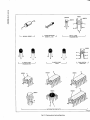
LOGIC FUNDAMENTALS
Digital logic techniques are used to perform many functions
within this instrument . The function and operation of the
logic circuits are described using logic symbology and terminology . This portion of the manual is provided to be an aid
in the understanding of these symbols and logic concepts,
not a comprehensive discussion of the subject.
Symbols
The symbols used to describe digital circuits in this instrument are based on ANSI standard Y32.14-1973 . Table 3-1
provides a basic reference for the logic devices used within
this instrument . Any deviations from the standard symbology, or devices not defined by the standard, are described
in the circuit description for the applicable device .
NOTE
Logic symbols used on the diagrams depict the
logic function as used in this instrument, and
may differ from the manufacturer's data.
Logic Polarity
All logic functions are described using the positive logic
convention . Positive logic is a system of notation where the
more positive of two levels (H I) is called the true or 1-state;
the more negative level (LO) is called the false or 0-state.
The HI-LO method of notation is used in this description .
The specific voltages that constitute a HI or LO state may
vary between individual devices. Wherever possible, the input and output lines are named to indicate the function
performed when at the HI (true) state.
Theory of Operation-7B80
Input/Output Tables
Input/Output (truth) tables are used to show the input
combinations important to a particular function, along with
the resultant output conditions . This table may be given
either for an individual device or for a complete logic stage.
For examples of input/output tables for individual devices,
see Table 3-1 .
NON-DIGITAL DEVICES
Not all of the integrated circuits in this instrument are digital logic devices. The function of nondigital devices is described individually, using operating waveforms or other
techniques to illustrate the function .
TIME/DIV
SOURCE
EXT TRIG
IN
ROW & COLUMN
DATA
TIME/DIV1
~READOUTJ
SIGNAL
(SWEEPI
OUTPUT
LEVEL
HOLDOFF
1986-60
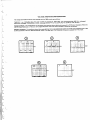
Fig. 3-1 . Basic block diagram of the 7B80 Time-Base Unit .
3-2
Theory of Operation-71380
TABLE 3-1
Basic Logic Reference
Description
Symbol
Device
AND gate
A
B
D
X
A device with two or more inputs
and one output . The output of the
AND gate is HI if and only if all of
the inputs are at the H I state.
Input/Output Table
Input
A
A
X
B
OR gate
A
X
e
A device with two or more inputs
and one output . The output of the
NAND gate is LO if and only if all
of the inputs are at the H I state.
A device with two or more inputs
and one output . The output of the
OR gate is HI if one or more of the
inputs are at the H I state.
A device with two or more inputs
and one output . The output of the
NOR gate is LO if one or more of
the inputs are at the H I state.
NOR gate
A
B
LO
LO
HI
LO
HI
HI
LO
A
HI
X
A device with one input and one
output . The output state is always
opposite to the input state.
LO
LO
Input
Output
A
B
LO
LO
LO
HI
HI
Hl
LO
HI
X
HI
HI
I
A
HI
LO
/Output
Input
X
B
LO
LO
LO
HI
HI
LO
HI
HI
LO
HI
HI
I
Input
A
LO
HI
X
HI
LO
HI
I
HI
Output
B
LO
HI
I nverter
X
B
LO
HI
NAND gate
/output
LO
HI
LO
I
LO
LO
Theory of Operation-71380
TABLE 3- 1 (cont)
Device
Symbol
Description
Input/Output Table
A small circle at the input or
output of a symbol indicates that
the LO state is the significant state.
Absence of the circle indicates that
the HI state is the significant state.
Two examples follow :
LO-state
indicator
AND gate with LO-state indicator
at the A input.
The output of this gate is HI if and
only if the A input is LO and the B
input is HI .
Input
A
/Output
B
X
LO
LO
LO
HI
LO
LO
LO
HI
HI
J
HI
HI
LO
OR gate with LO-state indicator at
the A input :
X
Dynamic
Indicator
a
Triggered
(toggle)
Flip-Flop
The output of this gate is HI if
either the A input is LO or the B
input is H I .
Indicates that this input (usually
the trigger input of a flip-top) responds to the indicated transition
of the applied signal .
A bistable device with one input
and two outputs (either or both
outputs may be used) . When triggered, the outputs change from one
stable state to the other stable state
with each trigger. The outputs are
complementary (i .e ., when one output is HI the other is LO). The
dynamic indicator on the trigger
(T) input may be of either polarity
depending on the device .
Input
/ Output
Condition Condition
before
after
trigger
trigger
pulse
pulse
Q
Q
HI
Q
HI
HI
LO
LO
LO
Q
LO
HI 1
Theory of Operation-71380
TABLE 3-1 (cont)
Device
Triggered
Set-Clear
(J-K)
Flip-Flop
D (data) Type
Flip-Flop
with Direct
Inputs
(Direct Inputs
may be
applied to all
triggered
flip-flops)
Symbol
Description
A bistable device with three or
more inputs and twu outputs
(either or both outputs may be
used). When gated, the outputs
change state in response to the
states at the inputs prior to the trigger. The outputs are complementary (i .e ., when one output is HI
the other is LO). The dynamic indicator on the gate (G) input may be
of either polarity depending on the
device .
A bistable device with two inputs
and two outputs (either or both
outputs may be used) . When clocked, the state of the Q output
changes to the state at the data (D)
input. The outputs are complementary (e .g ., when one output is HI
the other is LO) . The dynamic indicator on the clock input may be of
either polarity, depending upon the
device .
For devices with set (S) or reset (R)
inputs, the indicated state at either
of these inputs overrides all other
inputs to the states shown in the
Input/Output Table .
Input/Output Table
Input
J
K
LO
LO
HI
LO
HI
HI
LO
HI
/ Output
Q
Q
LO
HI
No change
HI
LO
Changes
state
Output conditions shown
after gate pulse.
Set (S) and reset (R) inputs override data (D)
and clock (C) inputs .
Input
R
S
HI
LO
/ Output
Q
I Q
I
LO
HI
LO I Undefined
H I I No Effect
HI I HI
LO
LO
HI
LO
Set (S) and Reset (R)
inputs both high .
Input
Output
Condition Condition
after
before
clock
clock
pulse
pulse
D
HI
LO
Q
HI
LO
Q
LO
HI
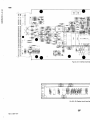
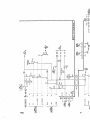
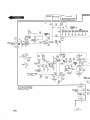
Fig. 3-2. Detailed block diagram of Trigger Generator.
Theory of Operation-71380
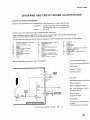
FRONT-PANEL DISTRIBUTION
The Front-Panel Distribution diagram shows the interconnections between front-panel functions (controls, connectors, and indicators) and circuit boards within this
instrument .
TRIGGER GENERATOR
The Trigger Generator provides a stable display by starting
the Sweep Generator (diagram 4) at a selected point on the
input waveform . The triggering point can be varied by the
LEVEL control and may be on either the positive or negative slope of the waveform . The triggering signal source
may be from either the signal being displayed (INT), a signal from an external source (EXT), or a sample of the
power-line voltage (LINE) . A block diagram of the Trigger
Generator is shown in Figure 3-2.
External Source
A sample of the line voltage is connected to the trigger circuits via interface connector pin A4 . The line signal is
connected to the Trigger Source Selector and Amplifier
stage at U65-pin 2.
Trigger Source Selector and Amplifier
The Trigger Source Selector and Amplifier stage (partial
U65) determines whether the triggering signal source is
from the signal being displayed (INT), a signal from an external source (EXT), or a sample of the power line voltage
(LINE) .
The trigger source is selected by SOURCE switch S50 by
connecting the most positive voltage to the source input of
U65 (refer to Figure 3-3) . The voltage offset from LEVEL
control R60 is coupled to U65-pin 10 . The differential trigger output signal from U65-pins 16 and 17 is coupled to the
Slope Selector and Trigger Generator stage (U85).
The external trigger signal is connected to the Trigger Generator through EXT TRIG IN connector J12. Push-button
switch S10 provides 10 times attenuation of the external
trigger input signal .
High-frequency reject coupling is provided in the Trigger
Source Selector stage . When the AC HF REJ push button is
pressed, C68 and components internal to U65-pin 9 form a
high-frequency rejection filter . Only low-frequency ac triggering signals are accepted .
When SOURCE switch (S50) is set to EXT, external signals
below approximately 16 kilohertz are coupled through R 15
and R20 to External Trigger Amplifier Q22. Ac coupling is
provided by C15. Triggering signals above 16 kilohertz are
coupled through C20 to the gate of Q22A .
Peak-to-Peak Auto
Field-effect transistors Q22A and Q22B form a unity-gain
source follower, which couples the external trigger signal to
the Trigger Source Selector and Amplifier stage (U65-pin 4) .
Diodes CR23 and CR24 provide input protection by clamping the input within a diode drop of ground (approximately
0.7 volt) .
Internal and Line Source
The internal trigger signal from the vertical channel of the
mainframe is connected to the Internal Trigger Amplifier
stage (U35) differentially via interface connector pins A20
and B20.
Internal trigger signals with frequencies above 16 kilohertz
are coupled through C37 directly into the Trigger Source
Selector and Amplifier stage (U65-pin 8) . Internal trigger
signals with frequencies below 16 kilohertz are coupled differentially through R31 and R33 to U35-pins 2 and 3. The
single-ended output at U35-pin 6 is coupled, along with the
offset from LEVEL control R60, to U65-pin 10 . Ac coupling is provided by C43.
The Peak-to-Peak Auto function can be divided into 3 distinct blocks . First, the Peak Detector determines signal size
and do positioning . Second, a DC Centering loop centers
the peak-detected output regardless of the do input and offset voltages . Third, the Peak-to-Peak Level Range output
voltage is automatically adjusted until the trigger output
reaches the clamp level set by the Automatic Gain Control
to achieve full level range (refer to the Specification section
in this manual for level range parameters) .
PEAK DETECTOR . The peak detector outputs from U65pins 14 and 15, rectified within U65, are externally filtered
by C73 and C74. Secondary stages of peak detection for
the positive and negative detector signals are provided by
U75A-CR71-C72 and U75B-CR75-C76. Outputs from the
Peak Detector stage are coupled to the Peak-to-Peak Level
Range and DC Centering stages .
DC CENTERING. Operational amplifier U55B adjusts the
input level at U65-pin 10 to null the do input voltage and
accumulated do offsets. This allows the trigger outputs at
U65-pins 16 and 17 to balance when LEVEL control R60 is
set to zero . DC Balance adjustment R85 provides centering
for offset voltages due to circuitry external to U65-pins 16
and 17 (e .g ., U85) .
3- 7
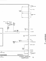
Theory of Operation-7880
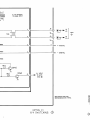
EXTERNAL INPUT
LINE INPUT
TRIGGER SOURCE
SELECTOR
PARTIAL
U65
17
16
INTERNAL INPUT
+TRIGGER
TRIGGER
1986-62
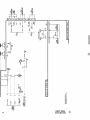
Fig. 3-3. Functional diagram of Trigger Source Selector.
PEAK-TO-PEAK LEVEL RANGE. The Peak-to-Peak Level
Range stage amplifies the peak Detector signals to provide
constant amplitude trigger signals and to determine the
range of the front-panel LEVEL control. Peak Detector signal amplitude is dependent on triggering (input) signal
amplitude.
Slope Selector and Trigger Generator
Peak Detector signals from R58-1159 are coupled to U55Apin 3 of the Peak-to-Peak Level Range stage. The gain of
the feedback amplifier (consisting of U55A and pins 1 and
20 of U65) increases as the Peak Detector signal amplitude
is reduced, thereby producing a constant trigger signal level
at U65-pins 16 and 17 .
SLOPE switch S60 is connected to U85-pin 1 to determine
whether the display is triggered on the positive-going or
negative-going slope. When the SLOPE switch is set to +, a
positive-going signal on pin 13 produces a positive-going
gate on pin 3 and a negative-going gate on pin 4. When the
SLOPE switch is set to -, a negative-going signal on pin 13
produces a positive-going gate on pin 3 and a negative-going
gate on pin 4. Slope Balance adjustment R80 provides optimum input balance for both + and - SLOPE-operation .
The range of the front-panel LEVEL control is zero at minimum triggering signal amplitude. The LEVEL range increases as triggering signal amplitude increases, until it
reaches maximum level range at the Automatic Gain Control threshold . Refer to the Specification section in this
manual for triggering sensitivity and triggering LEVEL
range parameters .
Automatic Gain Control . The Automatic Gain Control
stage limits the trigger signal amplitude to approximately
450 millivolts peak-to-peak (at U65-pins 16 and 17) regardless of the trigger input signal amplitude. The level of the
peak detected signal from R58-1159 is sensed by a feedback
amplifier stage (U55A and pins 1 and 20 of U65) . When the
peak detected signal is above the Automatic Gain Control
threshold (resulting from approximately 2 divisions of internal trigger signal or approximately 50 millivolts external
trigger signal), the Automatic Gain Control stage limits the
output trigger signal amplitude at U65-pins 16 and 17 . Current into U65-pin 3 (established by R51) determines the
current reference that sets the Automatic Gain Control
threshold .
Integrated circuit U85 converts the differential trigger signal from the Trigger Source Selector and Amplifier block to
a differential gate waveform for use by the Gate Generator
stage .
The delay mode control signal into U85-pin 16 is functional
only when the unit is operating as a delayed sweep unit in
the B Horizontal compartment of a mainframe with 2 horizontal compartments . When the unit is operating in the
independent or triggerable after delay time modes (as determined by the delaying sweep time-base unit in the A horizontal compartment), there is no effect on the Trigger
Generator circuits . However, when the unit is operating in
the B starts after delay time mode, a HI level at U85-pin 16
supplies a trigger gate pulse to U85-pins 3 and 4 in the absence of a trigger disable pulse at pins 6 and 10 .
At the end of each sweep, the Logic circuits (diagram 3)
supply a trigger disable pulse through Q242 to U85-pins 6
and 10 . A HI level disables the Trigger Generator to allow
enough time for the sweep generator to stabilize before another trigger pulse starts the next sweep.
Theory of Operation-71380
Gate Generator
The Gate Generator stage provides an auto enable gate to
the Logic circuits (diagram 3), and a sweep start gate and
Z-axis gate (unblanking) to the Sweep Generator circuit
(diagram 4) . Refer to Figure 3-4 for a timing diagram of the
Gate Generator functions.
When an adequate trigger signal is applied to U85-pins 13
and 14, a HI level is produced at U85-pin 3 and a LO level
is produced at U85-pin 4.
In the absense of a trigger output at U85-pins 13 and 14,
pin 3 is set LO and pin 4 is set HI . The LO level from U85pin 3 is coupled through J200-2 to the Logic circuit (diagram 3) to indicate the lack of a triggering signal . The Logic
circuit provides a LO-level auto sense pulse through J200-3
to the base of Q98. This LO level gates the comparator
(Q98 and Q96) . The collector of Q98 rises high to provide a
sweep start gate and the collector of 096 falls LO to provide a Z-axis gate (unblanking) at J200-4 .
LOGIC
The HI level from U85-pin 3 is coupled through emitter
follower Q88 and J200-2 into the Logic circuit (diagram 3)
to indicate that a triggering signal has been received . The
Logic circuit (diagram 3) sets the auto sense at J200-3 H I,
turning off Q98. Simultaneously, the LO level at U85-pin 4
gates comparator Q96-Q92. The collector of Q92 rises HI
to provide a sweep start gate at J200-5 and the collector of
Q96 falls LO to provide a Z-axis gate (unblanking) at
J200-4 .
AUTO MODE OPERATION
WITH TRIGGER SIGNAL
O3
The Logic circuit controls the sweep modes and associated
functions of the time-base unit (e .g ., sweep display, hold
off, auto sweep, single sweep, etc.) . The Logic circuit also
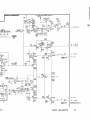
generates control signals for the mainframe. A block diagram for the Logic circuit is shown in Figure 3-5.
Sweep Modes
Integrated circuit U220 controls the NORM, AUTO, and
SINGLE SWEEP MODES and also generates control signals
used in the 71380. P-P AUTO operation is described in the
Trigger Generator circuit description (diagram 2) .
AUTO MODE OPERATION
WITHOUT TRIGGER SIGNAL
GATE
U85 PIN 3
GATE
U85 PIN 4
u
AUTO
J200-3
SWEEP START
GATE
J200-5
I
I
I
1
I
I
I
I
1
I
I
I
I
I
I
I
I
I
I
I
AUTO ENABLE
GATE
J200-2
Z-AXIS GATE
J200-4
I
I
u
I
I
I
I
I
I
1
U
I
I
1
I
0
I
I
I
1
I
I
I
~
~
I
I
I
I
I
I
I
I
z
I
I
I
I
i
I
U
I
I
I1
I
I~
~
I
I
II
1
1
1986-63
Fig. 3-4. Timing diagram for Gate Generator stage (092, Q96, 098) .
3- 9
Theory of Operation-71380
NORMAL MODE . The NORM MODE is provided when
U220-pin 12 is LO . In the NORM MODE, only an appropriate trigger signal can initiate a sweep gate to the Sweep
Generator (diagram 4) . Sweep Control integrated circuit
U220 controls sweep lockout and hold off functions.
AUTO MODE . The Auto Control stage produces a freerunning reference trace (bright base line) in the absence of a
trigger signal .
A HI level from MODE switch S230 is inverted by Q230 to
U220-pin 19 LO, which selects AUTO MODE operation . In
the presence of a trigger pulse from the Trigger Generator
(diagram 2), a HI level at U220-pin 1 discharges the auto
stage which inhibits the auto sense signal from U220-pin 3 .
In the absence of a trigger pulse, the LO level at U220-pin 1
an auto sense signal is initiated from U220-pin 3 to the
Trigger Generator (diagram 2) .
SINGLE SWEEP MODE . SINGLE SWEEP operation provides display of only one sweep. After one sweep has run,
all othersweepsare inhibited until the SINGLE SWP-RESET
push button is pressed . The READY light indicates when
the sweep is ready to accept a trigger .
After completion of one sweep, the hold off start pulse at
U220-pin 16 causes the sweep disable out at pin 17 to rise
HI . A HI level at U220-pin 12 initiates single sweep operation and holds the sweep disable out at U220-pin 17 HI
after completion of the sweep. Momentary contact of the
RESET push button places a LO at U220-pins 14 and 15,
which removes the sweep disable out from pin 17 and
allows the Sweep Generator (diagram 4) to accept a trigger.
Interface connector 1315 provides a remote single-sweep reset input from compatible mainframes .
Hold Off Timing
The hold off stages prevent the Sweep Generator (diagram
4) from being retriggered until the sweep timing capacitors
are discharged .
At the end of each sawtooth waveform from the Sweep
Generator (diagram 4), a sweep stop comparator pulse (H I)
is coupled to U220-pin 16 . This pulse enables the hold off
timing circuits at U220-pin 8, which sets the sweep disable
out at U220-pin 17 HI and the hold off signal at pin 10 LO
for the duration of the hold off cycle. Hold off timing
(U220-pin 8) is provided by capacitors C212 through C215,
and resistors R212 through R214 . Transistors Q203 and
TRIG'D
TIME/DIV
C 1986-64
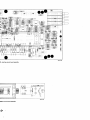
Fig. 3-5. Detailed block diagram of Logic circuit.
3- 10
Theory of Operation-71380
Q204 prevent the sweep disable out pulse at U220-pin 17
from falling LO until the timing capacitors have discharged .
Transistors Q212 and Q214 and front-panel HOLD OFF
control R210 provide variable current to the timing components to change the hold off time period .
Lockout Buffer Amplifier
A lockout pulse (HI) may be initiated at interface connector pin B8 by mainframe switching functions. A HI level,
coupled from interface connector B8 through the Lockout
Buffer Amplifier (Q201, Q202, and Q206) to the lockout
input at U220-pin 18, initiates a sweep disable pulse at
U220-pin 17 thereby disabling the sweep . The lockout
pulse (H I) is also applied through Q358 (diagram 4) to the
hold off start input at U220-pin 16 to enable the hold off
cycle.
Hold Off Output Amplifier
The Hold Off Output Amplifier inverts and amplifies the
hold off signal from U220-pin 10 for use by the mainframe.
Transistor Q272 inverts the hold off signal from U220-pin
10 to provide a H I level when hold off is present. The inverted signal is coupled through emitter follower Q274 to
interface connector B4 .
SWEEP GENERATOR
4O
The Sweep Generator produces a linear ramp waveform for
the mainframe when gated by the Trigger Generator. A
sweep gate (unblanking) is also generated in this circuit
block .
The linear sweep ramp waveform is produced by charging a
capacitor from a constant current source . The slope of the
ramp determines the sweep rate of the displayed trace . A
block diagram of the Sweep Generator is shown in
Figure 3-6.
Timing Current Source
The Timing Current Source stages generate a constant current for the Ramp Generator stages (see Figure 3-6) .
A Reference Voltage Source is established by the +50 volt
supply and R710, R711, R717, and R705 (front-panel SWP
CAL adjustment) .
The reference voltage is applied to the Source Current Generator stage. Operational amplifier U722 provides unity
voltage gain and low output impedance. The output of
U722 is connected through the base-emitter junction of
Q732 to the Timing Resistors (R741 through R749). Timing current is the result of the voltage drop across the
REV . A, APR . 1976
Timing Resistors and flows through the collector of Q732
to the Ramp Generator stages .
Ramp Generator
The Ramp Generator stages produce a linear positive-going
ramp for the Output Preamplifier and Sweep Gate Generator stages . Refer to Figure 3-6.
Upon the arrival of a HI-level sweep start gate at the Current Switch stage, Q322 turns on and Q324 turns off. The
source current from Q732 charges the Timing Capacitors
(C332, C334, C336) in a positive ramp . Field effect transistors Q334A, Q334B, and transistor Q338 form a unity-gain
Ramp Voltage Follower for the sweep ramp . The output of
Q338 is connected to the Horizontal Preamplifier, Sweep
Stop Comparator, and Baseline Stabilizer stages .
When the sweep start gate is LO, Q322 turns off and Q324
turns on causing the Timing Capacitors (C332, C334, and
C336) to discharge. The Baseline Stabilizer stage (Q304,
Q314) maintains a constant level from which the ramp begins . The output of Q338 is compared (by way of Q304A)
with the reference level at the base of Q304B. If the output
of Q338 is less than the reference, Q314 will charge the
timing capacitors through CR323 until the output and reference voltages are equal. If the output of Q338 is greater
than the reference, Q314 conducts more and CR323 conducts less causing the Timing Capacitors to discharge
through Q324 and R322 . When the output and reference
voltages are equal, the current through CR323 and Q732
equals the current through Q423 .
Output Preamplifier
The Output Preamplifier stages connect the differential
sweep signal to the mainframe and provide an offset voltage
for trace positioning . Provisions are made in these stages for
sweep magnification, and a negative-going sawtooth signal is
supplied to the mainframe for sawtooth output and special
plug-in unit functions. Refer to Figure 3-6.
The sweep ramp voltage from Q338 is coupled to the Horizontal Preamplifier stage at the base of Q424 . Transistors
Q424 and Q434 form a single-ended to push-pull converter
with Q428 and Q438 as current follower stages for the
push-pull signal . Output drivers Q448 and Q458 provide
final amplification and connect the sweep signal to the
mainframe.
The MAG switch, S435, increases the Horizontal Preamplifier gain ten times by connecting R431 and R430 in parallel
with R442 .
3- 1 1
Fig. 3-6. Detailed block diagram of Sweep Generator .
Fig. 3-6. Detailed block diagram of Sweep Generator (cont.) .
Theory of Operation-71380
The Position Voltage Source stage combines the do voltages
of the FINE and POSITION controls for a position voltage
level at the output of operational amplifier U416 . This voltage level on the base of Q434 provides a ramp waveform
offset voltage to horizontally position the displayed trace.
TIME/DIVISION READOUT O5
The Readout circuits provide information to the mainframe
readout system . Readout circuitry is shown on the Time/
Division Readout (diagram 5) at the rear of this manual .
Basic Readout System
The Auxiliary Sweep Preamplifier stage provides a negativegoingsweep ramp to the mainframe (via interface connector
pins-A3 and 133) for sawtooth output and special plug-in
unit functions. Transistors Q344 and Q346 form a unitygain inverting amplifier for the sawtooth signal from the
Ramp Voltage Follower stage. Diode CR344 provides
emitter-base compensation .
Sweep Gate Generator
The Sweep Gate Generator produces an unblanking gate for
the Z-axis system of the mainframe. When the sweep is displayed, the crt is unblanked (gate level LO) . The sweep is
blanked (gate level H I) between sweeps . Refer to Figure 3-6.
The sweep ramp is applied to the Sweep Stop Comparator
stage. A comparison voltage is set at the base of Q356 .
When the ramp voltage exceeds the comparison voltage,
Q352 turns off and Q356 couples a HI level through
common-base transistor Q358 . The Sweep Stop Comparator
output is coupled to the Sweep Gate Generator stage and to
the Logic circuit (diagram 3) to initiate hold off.
The readout system in 7000-series mainframes provides
alpha-numeric display of information encoded by the plugin units. This display is presented on the crt, and is written
by the crt beam on a time-shared basis with the analog
waveform display.
The readout system produces a pulse train consisting of ten
negative-going pulses called time-slots . Each pulse represents
a possible character in a readout word, and is assigned a
time-slot number corresponding to its position in the word .
Each time-slot pulse is directed to one of ten output lines,
labeled TS 1 through TS 10 (time slots one through ten),
which are connected to the vertical and horizontal plug-in
compartments . Two output lines, row and column, are connected from each channel (two channels per plug-in compartment) back to the readout system .
Data is encoded on these output lines either by connecting
resistors between them and the time-slot input lines or by
generating equivalent currents . The resultant output is a
sequence of analog current levels on the row and column
output lines . The row and column current levels are decoded by the readout system to address a character matrix
during each time slot, thus selecting a character to be displayed or a special instruction to be followed .
INTERFACE CONNECTO
POWER SUPPLY
The Z-axis gate from the Trigger Generator circuit (diagram
2) is LO at the start of the sweep. This LO level turns off
Q372 . The resultant HI-level sweep gate pulse at the collector of Q372 is coupled through emitter follower Q382 to
the mainframe for sweep unblanking . At the end of the
sweep, the HI level from the Sweep Stop Comparator stage
turns Q362 off and Q372 on . The resultant LO is coupled
through emitter follower Q382 to the mainframe for sweep
blanking .
The Interface Connectors provide interconnection for control signals and power supply voltages between the mainframe and the time-base unit .
The Power Supply derives supply voltages from the mainframe supplies for power requirements unique to this
instrument . Additional voltage regulation is also provided .
Theory of Operation-71380
TABLE 3-2
Readout Character Selection
Characters
Time-Slot
Encoded By
Description
Decimal
TS-1
Determines decimal magnitude
(number of zeros displayed or
prefix change information) .
R751,13752
13756
Uncalibrated
(>)
TS-3
Indicates calibrated or uncalibrated sweep rates and delay
times.
13761, 13764
1, 2, 5
TS-4
Scaling (TIME/DIV) .
13771
13772, 13773
m, p, n
TS-8
Defines the prefix which modifies
the units of measurement.
13781, 13782
13783, 13784
s (seconds)
TS-9
Defines the unit of measurement.
I
R793,13794
Section 4-71380
MAINTENANCE
This section of the manual contains information for performing preventive maintenance, troubleshooting, and corrective
maintenance for this instrument .
PREVENTIVE MAINTENANCE
Preventive maintenance consists of cleaning, visual inspection, lubrication, etc. Preventive maintenance performed on a regular basis may prevent instrument breakdown and will improve the reliability of the instrument . The severity of the environment to which this instrument is subjected determines the frequency of maintenance. A convenient time to perform
preventive maintenance is preceding adjustment of the instrument .
CLEANING
This instrument should be cleaned as often as operating
conditions require. Accumulation of dirt on components
acts as an insulating blanket and prevents efficient heat
dissipation which can cause overheating and component
breakdown.
Avoid the use of chemical cleaning agents which
might damage the plastics used in this instrument. In particular, avoid chemicals that contain
benzene, toluene, xylene, acetone, or similar
solvents.
Exterior
Loose dust accumulated on the front panel can be removed
with a soft cloth or small brush. Dirt that remains can be removed with a soft cloth dampened with a mild detergent
and water solution . Abrasive cleaners should not be used .
Interior
Dust in the interior of the instrument should be removed
occasionally due to its electrical conductivity under highhumidity conditions . The best way to clean the interior is
to blow off the accumulated dust with dry, low-pressure
air. Remove any dirt which remains with a soft brush or a
cloth dampened with a mild detergent and water solution .
A cotton-tipped applicator is useful for cleaning in narrow
spaces .
Switch Contacts
Switch contacts and pads are designed to operate dry for
the life of the switch . However, as the switches are not
sealed, dust attracted to the contact area may cause switch
contacts to become electrically noisy. Cleaning may be
accomplished by flushing the contact area with isopropyl
alcohol or kelite (1 part kelite to 20 parts water) . Do not
use chemical cleaning agents that leave a film or that might
damage plastic parts. Do not use cotton swabs or similar
applicators to apply cleaning agents, as they tend to snag
and leave strands of cotton on switch contacts . Should it
become necessary to remove a switch for replacement or
cleaning, refer to Component Removal and Replacement in
this section.
VISUAL INSPECTION
This instrument should be inspected occasionally for such
defects as broken connections, improperly seated semiconductors, damaged circuit boards, and heat-damaged parts.
The corrective procedure for most visible defects is obvious;
however, particular care must be taken if heat-damaged
components are found. Overheating usually indicates other
trouble in the instrument ; therefore, it is important that the
cause of overheating be corrected to prevent recurrence of
the damage .
LUBRICATION
Generally, there are no components in this instrument that
require a regular lubrication program during the life of the
instrument .
Maintenance-71380
Cam Switch Lubrication
In most cases, factory lubrication should be adequate for
the life of the instrument . However, if the switch has been
disassembled for replacement of switch sub-parts, a lubrication kit containing the necessary lubricating materials and
instructions is available through any Tektronix Field Office .
Order Tektronix Part 003-0342-01 . General Electric Versilube © silicone grease should be applied sparingly so that
the lubricant does not get on the contacts . Refer to Figure
4-1 for lubrication instructions .
SEMICONDUCTOR CHECKS
Periodic checks of the semiconductors in this instrument
are not recommended . The best check of semiconductor
performance is actual operation in the instrument . More
details on checking semiconductor operation are given
under Troubleshooting.
ADJUSTMENT AFTER REPAIR
After any electrical component has been replaced, the adjustment of that particular circuit should be checked, as
well as the adjustment of other closely related circuits . The
Performance Check and Adjustment procedure in this
manual provides a quick and convenient means of checking
instrument operation. In some cases, minor troubles may be
revealed or corrected by adjustment .
O
O
O
Apply lubricant to the drum journals and
mating surface in the mounting bearings .
Apply lubricant to the wear surface of the
index wheel .
Apply lubricant to the index roller and roller
guide in the front bearing. A thin film should
be applied to the inner face of the detent
springs if more than one spring is replaced .
Ensure that some lubricant is present at the
interface between the bearing and retainer clip .
C1967-2
Fig. 4- 1 . Lubrication procedure for a typical cam switch .
Maintenance-71380
TROUBLESHOOTING
The following information is provided to help troubleshoot this instrument . Information contained in other sections of this
manual should be used along with the following information to aid in locating the defective component. An understanding of
the circuit operation is very helpful in locating troubles, particularly where integrated circuits are used .
TROUBLESHOOTING AIDS
Diagrams
four significant digits of the JEDEC or vendor number
using the resistor color-code system (e .g ., a diode color
coded yellow-brown-green-red indicates a 1 N-4152 diode) .
Circuit diagrams are given on foldout pages in Section 8.
The component number and electrical value of each component in this instrument is shown on the diagrams .
Components that are mounted on circuit boards are outlined on the diagrams with a heavy black line .
Wiring Color Code
Voltages and Waveforms
Semiconductor Basing
Typical operating voltages are shown on the diagrams .
Voltage Conditions given on the diagram page indicate the
test equipment used and the front-panel control status
necessary to obtain the given voltages .
Typical operating waveforms are shown next to the diagram
where they were measured . Each waveform is numbered to
locate on the diagram the point where the waveform was
taken . Waveform Conditions given on the diagram page list
the test equipment used and the front-panel control status
necessary to obtain the given waveform .
Circuit-Board Illustrations
Circuit-board illustrations are shown on the foldout page
preceding the associated diagram . Each board-mounted
electrical component is identified by its circuit number, as
are interconnecting wires and connectors .
Figure 8-2, in the front of the diagrams section, shows the
location and assembly number of each circuit board in this
instrument .
Switch Cam Identification
Switch cam numbers shown on diagrams indicate the position of each cam in the complete switch assembly . The
switch cams are numbered from front to rear .
Diode Color Code
The cathode end of each glass-encased diode is indicated by
a stripe, a series of stripes, or a dot. The cathode and anode
ends of metal-encased diodes are identified by the diode
symbol marked on the case . For most silicon or germanium
diodes with a series of stripes, the color code identifies the
Insulated wire and cable used in this instrument is colorcoded to facilitate circuit tracing.
Figure 4-2 illustrates the basing configurations for all semiconductors used in this instrument . Some plastic-case
transistors have lead configurations that do not agree with
those shown here . If a replacement transistor is made by a
different manufacturer than the original, check the manufacturer's basing diagram. All transistor sockets in this
instrument are wired for the standard basing used for metalcase transistors .
Inter-Board Pin Connector Identification
The inter-board pin connector sockets are installed on circuit boards, in groups of 5 sockets (as in Figure 4-3) .
Socket number 1 is indexed on the circuit board with either
a triangular mark or the number 1 . Each group of sockets is
identified by its J (jack) number etched on the circuit
board . The J numbers correlate to the J (jack) and P (plug)
circuit numbers on the schematic diagrams .
Multi-Pin Connector Identification
Multi-pin connectors mate with groups of pins soldered to
circuit boards . Pin number 1 is indexed with a triangular
mark on the circuit board and molded on the holder of the
multi-pin connector, as shown in Figure 4-4. Each group of
pins is identified by its corresponding J number etched on
the circuit board . The J numbers, on the circuit boards,
correlate to the J and P component numbers on the schematic diagrams .
Interface Connector Pin Locations
The Interface circuit board couples the plug-in unit to the
associated mainframe (oscilloscope) . Figure 4-5 identifies
the pins on the interface connector as shown on Interface
Connectors and Power Supply diagram 8 in the Diagrams
section.
4- 3
Fig. 4-2. Semiconductor lead configuration.
Fig. 4-4. End-lead multi-pin connector assembly .
Fig. 4-3. Inter-board multi-pin connector assembly .
Performance Check and Adjustment
The Performance Check and Adjustment procedure, given in
section 5 of this manual, provides a quick and convenient
means of checking instrument operation . In some cases,
minor troubles may be revealed or corrected by adjustment .
TROUBLESHOOTING EQUIPMENT
The following equipment, in addition to that listed in the
Performance Check and Adjustment section, is useful for
troubleshooting.
Transistor Tester
Description : Dynamic-type tester .
Purpose : Test semiconductors .
Fig. 4-5. Location of pin numbers on Interface connector.
Maintenance-71380
Transistor Tester (Cont.)
Recommended Tektronix types: 576 Curve Tracer,
577/177 Curve Tracer system, 7CT1 N Curve Tracer
unit and a 7000-series oscilloscope system, or a
5CT1 N Curve Tracer unit and a 5000-series oscilloscope.
Multimeter
Description : Voltmeter, 10 megohm input impedance and a range from 0 to at least 50 volts dc ;
accuracy, within 0.1%. Ohmmeter, 0 to 20 megohms.
Test probes should be insulated to prevent accidental
shorting .
Purpose : Check voltage and resistance .
Test Oscilloscope
Description : Frequency response, do to 100 megahertz minimum ; deflection factor, 5 millivolts to
5 volts/division . A 10X, 10 megohm voltage probe
should be used to reduce circuit loading.
Purpose: Check operating waveforms.
TROUBLESHOOTING TECHNIQUES
The following troubleshooting procedure is arranged to
check the simple trouble possibilities before proceeding
with extensive troubleshooting . The first few checks ensure
proper connection, operation, and adjustment . If the
trouble is not located by these checks, the remaining steps
aid in locating the defective component. When the defective
component is located, it should be replaced using the replacement procedure given under Corrective Maintenance.
Troubleshooting Procedure
1 . CHECK CONTROL SETTINGS . Incorrect control settings can indicate a trouble that does not exist. If there is
any question about the correct function or operation of
any control, see the Operating Instructions, section 2.
2. CHECK ASSOCIATED EQUIPMENT. Before troubleshooting, check that the equipment used with this instrument is operating correctly. Check that the signal is properly connected and that the interconnecting cables are not
defective. Also, check the power source . If the trouble
persists, the time-base unit is probably at fault.
3. VISUAL CHECK . Visually check the portion of the
instrument in which the trouble is located. Many troubles
can be located by visible indications such as unsoldered
connections, broken wires, damaged circuit boards,
damaged components, etc.
4. CHECK INSTRUMENT ADJUSTMENT. Check the adjustment of this instrument, or the affected circuit if the
trouble appears in one circuit. The apparent trouble may be
the result of misadjustment. Complete adjustment instructions are given in the Performance Check and Adjustment,
section 5 .
5. ISOLATE TROUBLE TO A CIRCUIT. To isolate
trouble to a circuit, note the trouble symptom. The symptom often identifies the circuit in which the trouble is
located . When trouble symptoms appear in more than one
circuit, check the affected circuits by taking voltage and
waveform readings . Incorrect operation of all circuits often
indicates trouble in the power supply . Check first for
correct voltages of the individual supplies . However, a
defective component elsewhere in the instrument can appear as a power-supply trouble and may also affect the
operation of other circuits .
Figure 4-6 provides a guide for locating a defective circuit.
Start at the top of the chart and perform the checks given
on the left side of the page until a step is found that does
not produce the indicated results . Further checks, or the
circuit in which the trouble is probably located, are listed
to the right of the step . The shaded blocks on the Troubleshooting Chart indicate circuit(s) that may cause instrument malfunction . The circuit(s) listed in shaded blocks are
discussed in detail in the Theory of Operation section of
this manual . This chart does not include checks for all
possible defects ; use steps 6 and 7 in such cases.
After the defective circuit has been located, proceed with
steps 6 and 7 to locate the defective component(s) .
6. CHECK VOLTAGES AND WAVEFORMS. Often the
defective component can be located by checking for the
correct voltages and waveforms in the circuit. Refer to the
diagrams section at the rear of the manual for typical voltages and waveforms.
Maintenance-71380
NOTE
Voltages and waveforms given on the diagrams
are not absolute and may vary slightly between
instruments. To obtain operating conditions
similar to those used to take these readings, see
the voltage and waveforms page adjacent to
each schematic diagram. Note the recommended
test equipment, front-panel control settings,
voltage and waveform conditions, and test
equipment cable connection instructions.
7 . CHECK INDIVIDUAL COMPONENTS . The following
procedures describe methods for checking individual components . Two-lead components that are soldered in place
are best checked by first disconnecting one end . This iso
lates the measurement from the effects of surrounding
circuitry .
To avoid component damage, disconnect the
power source before removing or replacing
semiconductors.
Transistors . The best check of transistor operation is
actual performance under operating conditions . A transistor
can be most effectively checked by substituting a new component or one that has been checked previously . However,
be sure that circuit conditions are not such that a replacement transistor might also be damaged . If substitute transistors are not available, use a dynamic tester . Static-type
testers are not recommended, since they do not check
operation under simulated operating conditions .
Integrated Circuits . IC's can be checked with a voltmeter,
test oscilloscope, or by direct substitution . A good understanding of circuit operation is desirable when troubleshooting circuits using IC's . Use care when checking voltages and waveforms around the IC's so that adjacent leads
are not shorted together. A convenient means of clipping a
test probe to the 14- and 16-pin IC's is with an IC test clip .
This device also serves as an extraction tool . The lead configuration for the semiconductors used in this instrument
are shown on a pullout page in the front of the diagrams
section .
Do not use an ohmmeter scale that has a high
internal current. High currents may damage
the diode .
Diodes . A diode can be checked for an open or shorted condition by measuring the resistance between terminals with
an ohmmeter scale having a low internal source current,
such as the R X 1 K scale . The resistance should be very
high in one direction and very low when the meter leads are
reversed .
The cathode end of each glass-encased diode is indicated by
a stripe, a series of stripes, or a dot . The cathode and anode
ends of metal-encased diodes are identified by the diode
symbol marked on the case . For most silicon or germanium
diodes with a series of stripes, the color code identifies the
four significant digits of the JEDEC or vendor number
using the resistor color-code system (e .g ., a diode colorcoded yellow-brown-green-red indicates a 1 N-4152 diode) .
Resistors . Check resistors with an ohmmeter . See the Replaceable Electrical Parts list for the tolerance of the
resistors used in this instrument . Resistors normally do not
need to be replaced unless the measured value varies widely
from that specified .
Inductors . Check for open inductors by checking continuity with an ohmmeter . Shorted or partially shorted
inductors can usually be found by checking the waveform
response when high-frequency signals are passed through
the circuit . Partial shorting often reduces high-frequency
response .
Capacitors . A leaky or shorted capacitor can usually be
detected by checking resistance with an ohmmeter on the
highest scale . Do not exceed the voltage rating of the capacitor . The resistance reading should be high after initial
charge of the capacitor . An open capacitor can best be detected with a capacitance meter or by checking that the
capacitor passes ac signals .
8 . REPAIR AND ADJUSTMENT . If any defective parts
are located, follow the replacement procedures given in
Corrective Maintenance . Be sure to check the performance
of any circuit that has been repaired or had any electrical
components replaced .
Fig . 4-6 .
71380 troubleshooting chart .
Maintenance-71380
CORRECTIVE MAINTENANCE
Corrective maintenance consists of component replacement and instrument repair. Special techniques required to replace
components in this instrument are given here .
OBTAINING REPLACEMENT PARTS
All electrical and mechanical part replacements can be obtained through your Tektronix Field Office or representative . However, many of the standard electronic components
can be obtained locally in less time than is required to order
them from Tektronix, Inc. Before purchasing or ordering
replacement parts, check the parts list for value, tolerance,
rating, and description .
NOTE
When selecting replacement parts, remember
that the physical size andshape of a component
may affect the performance of the instrument,
particularly at high frequencies. All parts
should be direct replacements unless a different
component will not adversely affect instrument
performance.
Some parts are manufactured or selected by Tektronix, Inc.
to satisfy particular requirements, or are manufactured to
specifications for Tektronix, Inc. Most of the mechanical
parts used in this instrument have been manufactured by
Tektronix, Inc. To determine the manufacturer of parts,
refer to parts list, Cross Index Mfr. Code Number to
Manufacturer .
The reliability and accuracy of this instrument can be maintained only if proper soldering techniques are used when repairing or replacing parts. General soldering techniques,
which apply to maintenance of any precision electronic
equipment, should be used when working on this instrument . Use only 60/40 rosin-core, electronic-grade solder .
The choice of soldering iron is determined by the repair to
be made . When soldering on circuit boards, use a 15- to
40-watt pencil-type soldering iron with a 1/8-inch wide,
wedge-shaped tip. Keep the tip properly tinned for best
heat transfer to the solder joint. A higher wattage soldering
iron may separate the wiring from the base material . Avoid
excessive heat ; apply only enough heat to remove the component or to make a good solder joint. Also, apply only
enough solder to make a firm solder joint; do not apply too
much solder .
All circuit boards, except the readout circuit
board, in this instrument are multilayer type
boards with a conductive path (s) laminated between the top and bottom board layers. All
soldering on these boards should be done with
extreme care to prevent breaking the connections
to the center conductor(s); only experienced
maintenance personnel should attempt repair
of these boards.
When ordering replacement parts from Tektronix, Inc ., include the following information :
1 . Instrument type .
2. Instrument serial number .
3. A description of the part (if electrical, include
circuit number).
For metal terminals (e .g ., switch terminals, potentiometers,
etc.), a higher wattage-rating soldering iron may be required .
Match the soldering iron to the work being done . For example, if the component is connected to the chassis or
other large heat-radiating surface, it will require a 75-watt
or larger soldering iron .
4. Tektronix part number .
SOLDERING TECHNIQUES
WARNING
J
To avoid electrical shock, disconnect the instrument from the power source before soldering.
The following techniques should be used to replace a component on a circuit board :
1 . Grip the component lead with long-nose pliers . Touch
the soldering iron to the lead at the solder connection . Do
not lay the iron directly on the board, as it may damage the
board.
4- 9
Maintenance-71380
2. When the solder begins to melt, gently pull the lead out.
If unable to pull out the lead without using force, try removing the other end of the component as it may be more
easily removed .
NOTE
The reason some component leads are troublesome to remove is due to a bend placed on each
lead during the manufacturing process. The bent
leads hold components in place during a process
that solders many components atone time.
If a component lead is extremely difficult to remove, it
may be helpful to straighten the leads on the back side of
the board with a small screwdriver or pliers while heating
the soldered connection .
The exploded-view drawing associated with the Replaceable
Mechanical Parts list may be helpful in the removal or disassembly of individual components or subassemblies . Component locations and circuit board locations are shown in
the Diagrams section .
Circuit Boards
If a circuit board is damaged beyond repair, replace the entire board assembly . Part numbers for completely wired
boards are given in the Replaceable Electrical Parts list .
A3-READOUT CIRCUIT BOARD. To remove the circuit
board, follow the procedure given in Figure 4-7 .
A2-TRIGGER CIRCUIT BOARD. To remove the circuit
board :
Use only enough heat to remove the component lead without removing the solder from the board . If it is desired to
remove solder from a circuit-board hole for easier installation of a new component, a solder-removing wick should be
used .
1 . Remove 3 inter-board multi-pin connectors (see Figure
4-3 for identification) .
3. Bend the leads of the new component to fit the holes in
the board. If the component is replaced while the board is
mounted in the instrument, cut the leads so they will just
protrude through the board. Insert the leads into the holes
so the component is firmly seated against the board (or as
positioned originally) . If it does not seat properly, heat the
solder and gently press the component into place .
3. Lift rear of circuit board away from frame and slide
board to the rear until push-button switches are clear of the
front panel.
2. Remove 2 screws from circuit board.
4. Note wire color on single-conductor shielded cables (see
Figure 4-8 for identification) and connector to which each
is attached .
4. Touch the iron to the connection and apply a small
amount of solder to make a firm solder joint. To protect
heat-sensitive components, hold the lead between the component body and the solder joint with a pair of long-nose
pliers or other heat sink .
To replace the circuit board, reverse the order of removal.
5. Clip any excess lead protruding through the board (if
not clipped in step 3) .
Al-INTERFACE CIRCUIT BOARD. To remove circuit
board :
6. Clean the area around the solder connection with a fluxremoving solvent. Be careful not to remove information
printed on the board.
COMPONENT REMOVAL AND REPLACEMENT
WARNING
To avoid electrical shock, disconnect the instrument from the powersource before replacing
components.
4- 1 0
5. Disconnect cables from back of circuit board.
1 . Remove Trigger and Digital Voltmeter circuit boards
using procedures given previously .
2. Set TIME/DIV knob to 2 ms position and VARIABLE
TIME/DIV knob to expose the set screw.
3. With hex-key wrench, loosen set screws in both knobs.
Remove knobs from shafts .
REV A, MAY 1978
REMOVE READOUT BOARD AS FOLLOWS:
1 . Note index of multi-pin connector attached to board and disconnect cable.
2. Loosen set screw on variable switch assembly .
3. Remove VARIABLE (CAL IN) TIME/DIV knob and attached shaft out the front of the instrument .
4. Remove the 8 securing screws from board.
5. Lift board away from cam switch assembly .
TO REPLACE READOUT BOARD, REVERSE THE ORDER OF REMOVAL.
Fig. 4-7. Readout board removal procedure.
4 . Note color of multi-pin connectors (see Figure 4-4 for
identification) and P numbers to which each connect . Disconnect all multi-pin connectors from board .
5 . Remove 4 screws that secure gray plastic rear panel to
instrument frame .
6 . Remove 6 screws that secure perimeter of board to instrument frame .
7 . Remove Interface circuit board through rear of
instrument .
To install the Interface circuit board :
1 . Guide TIME/DIV switch shaft through hole in frontpanel .
2 . Install 6 screws that secure perimeter of board to instrument frame .
Maintenance-71380
3. Install gray plastic rear panel with 4 securing screws .
4. Replace TIME/DIV knob on shaft. Align knob index
with 2 ms position ; then, tighten 2 set screws on knob .
5. Replace VARIABLE knob and tighten set screw .
6. Replace all cables as noted during removal procedure.
7. Replace Trigger circuit board.
Switches
Two types of switches are used in this instrument . Contact
alignment and spacing are critical to the operation of the
push-button and cam switches . Therefore, defective
switches should either be replaced as a unit or repaired only
by personnel experienced with these types of switches .
Your local Tektronix Field Office or representative can provide additional repair information . The following special
maintenance information is provided for switch replacement .
CAM SWITCHES . Cam switches consist of a rotating cam
that mates with contacts on the adjacent circuit board .
These contacts are activated by lobes on the cam as the
switch is rotated. A cam switch can be disassembled for inspection, cleaning, repair, or replacement ; however, it is
recommended that the switch be removed and replaced as a
unit . Refer to Figure 4-9 for special instructions on cam
switch removal.
Repair of a cam switch should be undertaken
only by experienced maintenance personnel.
Switch alignment and contactspacing must be
carefully maintained for proper operation. A cam
switch repair kit is available (Tektronix part
040-0541-00) which contains special alignment
tools for use in repairing or replacing the switch
contacts. For information or assistance on
maintenance of cam switches, contact your local
Tektronix Field Office or representative.
PUSH-BUTTON SWITCHES . Removal and replacement instructions for push-button switches are shown in
Figure 4-10 .
Fig. 4-8. Coaxial end-lead connector assembly.
Semiconductors
To avoid component damage, power must be
turned off before removing or replacing
semiconductors.
Semiconductors should not be replaced unless actually defective. If semiconductors are removed during routine maintenance, return them to their original sockets. Unnecessary
replacement of semiconductors may affect the adjustment
of this instrument . When semiconductors are replaced,
check the operation of that part of the instrument which
may be affected .
Maintenance-71380
Handle silicone grease with care. Avoid getting
silicone grease in eyes. Wash hands thoroughly
after use.
END-LEAD PIN CONNECTORS . The pin connectors used
to connect the wires to the interconnecting pins are
clamped to the ends of the associated leads. To remove and
replace damaged end-lead pin connectors, remove the old
pin connector from the end of the lead and clamp the replacement connector to the lead .
Replacement devices should be of the original type or a
direct replacement . Figure 4-2 shows the lead configurations of the semiconductor devices used in this instrument.
Some plastic-case transistors have lead configurations that
do not agree with those shown here . When replacing, check
the manufacturer's basing diagram for correct basing. All
transistor sockets in this instrument are wired for the standard basing used for metal-case transistors . Semiconductors
that have heat radiators use silicone grease to increase heat
transfer . Replace the silicone grease when replacing these
semiconductors .
Some of the pin connectors are grouped together and
mounted in a plastic holder ; the overall result is that these
connectors are removed and installed as a multi-pin connector (see Figure 4-4) . To provide correct orientation of this
multi-pin connector when it is replaced, an arrow is marked
on the circuit board and a matching arrow is molded into
the plastic holder of the multi-pin connector. Be sure these
arrows are aligned as the multi-pin connector is replaced .
If the individual end-lead pin connectors are removed from
the plastic holder, note the color of the individual wires for
replacement .
An extraction tool should be used to remove the 14- and
16-pin integrated circuits to prevent damage to the pins .
This tool is available from Tektronix, Inc . Order Tektronix
part 003-0619-00 . If an extraction tool is not available
when removing one of these integrated circuits, pull slowly
and evenly on both ends of the device . Try to avoid having
one end of the integrated circuit disengage from the socket
before the other, as the pins may be damaged .
INTER-BOARD MULTI-PIN CONNECTOR . The interboard multi-pin connector pin-holder is not repairable and
should be replaced as a unit (see Figure 4-3) . Refer to the
Replaceable Mechanical Parts list for part number . Interboard multi-pin connector pin-sockets are soldered to
circuit boards (see Figure 4-3) . To replace a socket, first
remove the guide. Then, remove the old socket using soldering techniques previously described . Solder the new socket
in place, making sure it will align properly with the interboard connector pins .
WARNING
Interconnecting Pins
Three methods of interconnection are used to connect the
circuit boards with other boards and components . When the
interconnection is made with a coaxial cable, a special endlead connector plugs into a socket on the board (Figure 4-8) .
When the interconnection is made with a wire lead, an endlead connector is used which mates with the interconnecting pin soldered into the board (Figure 4-4) . When the
interconnection is made between adjacent boards, an interboard multi-pin connector is used (Figure 4-3) . The
following information provides the removal and replacement
procedure for the various types of interconnection methods.
COAXIAL END-LEAD CONNECTORS . Replacement of
the coaxial-type end-lead connectors requires special tools
and techniques ; only experienced maintenance personnel
should attempt to remove and replace these connectors . It
is recommended that the cable be replaced as a unit . For
cable part numbers, see the Replaceable Mechanical Parts
list . An alternative solution is to refer the replacement of
the defective connector to your local Tektronix Field
Office or representative .
CIRCUIT-BOARD PINS .
All circuit boards in this instrument, except the
Readout circuit board, are multilayer type boards
with a conductive path (s) laminated between
the top and bottom board layers. A// soldering
on these boards should be done with extreme
care to prevent breaking the connection to the
center conductor(s) ; only experienced maintenance personnel should attempt repair of these
boards.
A circuit-board pin replacement kit including the necessary
tools, instructions, and replacement pins is available from
Tektronix, Inc. Order Tektronix part 040-0542-00. Replacement of circuit-board pins on multi-layer boards is
not recommended ; refer such repairs to your local Tektronix Field Office or representative .
Fig. 4-9. Cam switch removal procedure .
Fig. 4-10 . Removal procedure for typical push-button switch .
Maintenance-71380
4-11) in the hole, if possible . If the ferrule remains in the
circuit board, remove the spare ferrule from the replacement pin and press the new pin into the hole in the circuit
board . If the ferrule is removed with the damaged pin, clean
out the hole using a solder-removing wick and a scribe .
Then, press the replacement pin with attached spare ferrule
into the hole . Position the replacement pin in the same
manner as the damaged pin . Solder the pin to the circuit
board on each side of the board . If the old pin was bent at
an angle to mate with a connector, carefully bend the new
pin to the same angle . Replace the pin connector .
Front-Panel Lights
This instrument uses LED's (light-emitting diodes) and incandescent lamps for front-panel lights .
LED's are used to illuminate the TRIG'D and SINGLE
SWP READY lights . To replace LED's, remove the cap
from the sleeve as in Figure 4-12 . Note lead wire color coding and LED lead configuration . Unsolder wire leads and
remove LED from the cap . Solder the replacement LED
and lead wires to the socket cap as noted previously . Install the cap in the sleeve .
Incandescent lamps are used to illuminate the transparent
push-button switches . To replace incandescent lamps, unsolder the lead wires from the rear of the cap (see Figure 412), pull the cap and bulb out of the sleeve . Solder the
replacement lamp and lead wires to the cap . Install the
assembly in the sub-panel sleeve .
ADJUSTMENT AFTER REPAIR
Fig . 4-11 . Exploded view of circuit-board pin and ferrule.
After any electrical component has been replaced, the
adjustment of that particular circuit should be checked, as
well as other closely related circuits . See Section 5 for a
complete adjustment procedure .
INSTRUMENT REPACKAGING
If the Tektronix instrument is to be shipped to a Tektronix
Service Center for service or repair, attach a tag showing :
owner (with address) and the name of an individual at your
firm that can be contacted, complete instrument serial
number and a description of the service required .
Save and re-use the package in which your instrument was
shipped . If the original packaging is unfit for use or not
available, repackage the instrument as follows :
Fig. 4-12 . Front-panel light socket assembly .
To replace a damaged pin which is mounted on a singlelayer circuit board, first disconnect any pin connectors .
Then (using Soldering Techniques given earlier in this
section), unsolder the damaged pin and pull it from the
board with a pair of pliers, leaving the ferrule (see Figure
4-16
1 . Obtain a carton of corrugated cardboard having inside
dimensions of no less than six inches more than the
instrument dimensions ; this will allow for cushioning .
The shipping carton test strength for this instrument is
200 I bs .
2 . Surround the instrument with polyethylene sheeting to
protect the finish of the instrument .
3 . Cushion the instrument on all sides by tightly packing
dunnage or urethane foam between carton and instrument, allowing three inches on all sides .
4 . Seal carton with shipping tape or industrial stapler .
REV . A, NOV . 1976
Section 5-71380
PERFORMANCE CHECK AND ADJUSTMENT
This section contains information necessary to perform a complete instrument performance check and adjustment . Limits
given in the procedure are adjustment guides and should not be interpreted as performance requirements unless preceded by a
check mark (-,/). Where possible, instrument performance is checked before an adjustment is made .
PRELIMINARY INFORMATION
Adjustment Interval
To maintain instrument accuracy, check the performance
of the 71380 every 1000 hours of operation, or every 6
months if used infrequently . Before complete adjustment,
thoroughly clean and inspect this instrument as outlined in
Section 4, Maintenance.
Tektronix Field Service
Tektronix Field Service Centers and the Factory Service
Center provide instrument repair and adjustment services .
Contact your Tektronix Field Office or representative for
further information .
Using This Procedure
PARTIAL PROCEDURES . The following procedure is
written to completely check and adjust the instrument to
the Performance Requirements listed in Section 2, Specification . If the applications for which the instrument is used
do not require the full available performance, the procedures
and the required equipment list can be shortened
accordingly .
A partial performance check and adjustment may be desirable after replacing components, or fo'touch up the adjustment of a portion of the instrument . To check or adjust
only part of the instrument, refer to the Equipment Required list which precedes that portion of the procedure to
be performed . To avoid unnecessary adjustment of other
parts, adjust only if the tolerance given in each CHECK is
not met.
TEST EQUIPMENT REQUIRED
This Performance Check and Adjustment procedure can be
used either for complete adjustment or as a check of instrument performance . Completion of each step in the procedure ensures that the instrument is correctly adjusted and
operating within specified limits. Refer to the following
discussion for instructions on a complete or partial check
and adjustment .
The test equipment listed in Table 5-1 is required for a
complete performance check and adjustment of this instrument . The specifications given in Table 5-1 for test equipment are the minimum required to meet the Performance
Requirements listed in Section 2, Specification . Detailed
operating instructions for test equipment are omitted in
this procedure . Refer to the test equipment instruction
manual if more information is needed .
INDEX. An index precedes the procedure to aid in locating
Performance Check and Adjustment steps.
Special Fixtures
PERFORMANCE CHECK. Instrument performance can be
checked by performing the complete Performance Check
and Adjustment procedure and omitting only the ADJUST
parts of the steps. A check mark (-,/) preceding a CHECK
indicates that the limit given is a performance requirement
specified in Section 2, Specification .
ADJUSTMENT . Completion of each step in the Performance Check and Adjustment procedure ensures that the
instrument is correctly adjusted and performing within
specified limits . Where possible, instrument performance is
checked before an adjustment is made . For best overall performance when performing the complete adjustment procedure, make each adjustment to the exact setting indicated.
Special fixtures are used only where they facilitate instrument adjustment . These fixtures are available from Tektronix, Inc. Order by part number from Tektronix Field
Offices or representatives.
Test Equipment Alternatives
The test equipment listed in the Examples of Applicable
Test Equipment column, Table 5-1, is required to check
and adjust this instrument . The Performance Check and Adjustment procedure is based on the first item of equipment
given as an example. If other equipment is substituted, control settings or setups may need to be altered. If the exact
item of equipment given as an example is not available,
refer to the Minimum Specifications column to determine if
other equipment may be substituted . Then check the
Purpose column . If you determine that your measurement
requirements will not be affected, the item and corresponding step(s) can be deleted.
Performance Check and Adjustment-71380
TABLE 5-1
Test Equipment
Examples of Applicable
Test Equipment
Description
Minimum Specifications
Purpose
1 . Oscilloscope Mainframe
Tektronix 7000-series . Bandwidth, 400 MHz with 2 horizontal plug-in compartments .
Provides a display for unit
under test .
a. Tektronix 7904 Oscilloscope
System .
2. Amplifier Plug-In Unit
Tektronix 7A-series. Bandwidth, 400 MHz; deflection
factor, 10 mV to 0.5 V.
Provides vertical input to
oscilloscope mainframe.
a. Tektronix 7A19 Amplifier
plug-in unit .
3. High-Frequency Signal
Generator
Frequency, 50 MHz to 400
MHz; output amplitude,
variable from 50 mV to 0.5 V
into 50 92 .
High-frequency triggering
checks .
a. SG 504 Leveled Sine Wave
Generator.
Marker outputs, 2 ns to 5 s;
accuracy, within 0.1%.
Sweep timing checks and
adjustments .
4. Time-Mark Generator
b. Wavetek 1002 Sweep/Signal
Generator.
a. Tektronix TG 501 Time-Mark
Generator with power module .
b. Tektronix 2901 Time-Mark
Generator.
c. Tektronix 184 Time-Mark
Generator.
5. Low-Frequency SineWave Generator
Frequency, 30 Hz to 50 kHz ;
output amplitude, variable
from 50 mV to 3 V into 50 92 .
:Low-frequency triggering
checks and adjustments .
6. Plug-In Extender
Tektronix 7000-series extender .
Provides access to internal
a. Tektronix 067-0589-00 Caliadjustments and test points . bration Fixture.
7. Coaxial Cables (2 required)
Impedance, 50 E2 ; type,
RG 58/U ; length, 42 and 18
inches ; connectors, BNC.
Provides signal interconnections .
a. Tektronix Part 012-0057-01 .
8. T Connector
Connectors, BNC.
External trigger checks and
adjustments .
a. Tektronix Part 103-0030-00.
9. Termination
Impedance, 50 E2 ; accuracy,
within 2% ; connectors, BNC.
Magnified sweep timing
check.
a. Tektronix Part 011-0049-01 .
10 . Screwdriver
3-inch shaft, 3/32-inch bit.
Adjustments.
a. Xcelite R-3323 .
5-2
a. Tektronix FG 503 Function
Generator with power module .
b. General Radio 1310-B
Oscillator.
REV A, MAY 1978
Performance Check and Adjustment-71380
INDEX TO PERFORMANCE CHECK AND
ADJUSTMENT PROCEDURE
PAGE
A. TRIGGERING SYSTEM
1 . Adjust DC Balance and Slope Balance
(1385, R80) .
5-4
5-4
N/ 2. Check Triggering Modes
5-4
-v/ 3 . Check External Level Range
5-5
~/ 5. Check Internal Triggering Sensitivity
5-6
N/ 4 . Check External Triggering Sensitivity
5-5
~/ 6. Check Internal Trigger Jitter
5-7
~/ 7. Check Line Triggering
5-7
B . HORIZONTAL SYSTEM
1 . Set Basic Sweep Calibration
5-8
5-8
2. Check Sweep Length and Positioning Range
3. Check/Adjust Magnifier Gain and Registration
(13430, 13445)
N/ 4. Check Variable Time/Division and Variable
Hold Off
5. Adjust Sweep Timing (C330, 13710, 13715)
6. Check Sweep Timing
7 . Check Magnified Sweep Timing
5-8
5-8
5-9
5-9
5-9
5-10
Performance Requirement check; see introductory information.
PRELIMINARY PROCEDURE
1 . Install an amplifier unit in the left vertical compartment
of the oscilloscope mainframe.
2. Install the 067-0589-00 plug-in extender in the B horizontal compartment of the mainframe. Remove the side
covers and install the 71380 in the plug-in extender.
3. Set the mainframe vertical mode switch to display the
left vertical unit and the horizontal mode switch to display
the B horizontal unit . Set the mainframe intensity controls
fully counterclockwise and set the trigger source switches
to vertical mode .
4. Turn on the mainframe and allow at least 20 minutes
warmup before beginning the procedure.
NOTE
The performance of this instrument can be
checked at any ambient temperature within the
0° to +50° C range unless stated otherwise. This
instrument must be adjusted at an ambient
temperature of +20° to +30° C for quoted
accuracy.
Performance Check and Adjustment-71380
A.
TRIGGERING SYSTEM
Equipment Required
1 . Oscilloscope mainframe .
6 . 50-ohm cables (2) .
2 . Amplifier plug-in unit .
7 . BNC T connector .
3 . Low-frequency sine-wave generator .
4 . High-frequency signal generator .
5 . Plug-in extender .
BEFORE YOU BEGIN, see
TEST POINT AND
ADJUSTMENT LOCATIONS
Control Settings
in the Diagrams section .
f . ADJUST-1385 (DC Balance) for a stable crt display .
Set the 71380 controls as follows :
TRIGGERING
MODE
P-P AUTO
COUPLING
AC
SOURCE
INT
h . ADJUST-1380 (Slope Balance) for a stable display .
POSITION
Midrange
TIME/DIV
20 Ms
i . Check for a stable display when the SLOPE switch is
set to (+) and (-) .
SWEEP
VARIABLE
IN (calibrated)
MAG
X1
HOLD OFF
MIN
A7 . ADJUST DC BALANCE AND SLOPE BALANCE
(1385, R80)
a . Connect the low-frequency sine-wave generator to the
amplifier unit input with a 50-ohm cable .
b . Set the oscilloscope mainframe intensity and focus
controls for the desired display .
c . Set the low-frequency sine-wave generator and the
amplifier unit deflection factor for a 0 .3-division display
at 50 kilohertz . Center the display vertically .
d . Set the TRIGGERING LEVEL control to approximately 0 (midrange) and TRIGGERING SLOPE to (+) .
e.
Check for a stable display with TRIG'D light on .
Performance Requirement check; see introductory information .
5-4
g . Set the SLOPE switch to (-) and check for a stable
display .
j . INTERACTION-Repeat the adjustment of R85 (DC
Balance) and R80 (Slope Balance) until a stable display
is obtained while changing TRIGGERING SLOPE .
NOTE
If any of the CHECK parts in the following steps
cannot be met, repeat step (A) 1 .
-\/ A2 . CHECK TRIGGERING MODES
a . Remove the 71380 and plug-in extender ; then install
the 71380 directly into the B horizontal compartment .
b . Set the low-frequency sine-wave generator and the
amplifier unit deflection factor for approximately a 2division display .
.\/ c . CHECK-For a stable display at all LEVEL control
settings (P-P AUTO MODE) .
Performance Check and Adjustment-71380
c. Set the amplifier unit deflection factor for 0.5 volts/
division . Set the low-frequency sine-wave generator for a
6-division display (3 volts) at 1 kilohertz .
d. Set the TRIGGERING MODE to AUTO .
N/ e. CHECK-Set the TRIGGERING LEVEL control for a
stable display (TRIG'D light on).
V f. CHECK-For a free-running display with TRIG'D
light off when the TRIGGERING LEVEL control is set
fully clockwise and fully counterclockwise .
~/ d. CHECK-That all levels of the positive slope may be
selected for the sweep starting point as the TRIGGERING LEVEL control is rotated throughout its range
(indicates an external level range of at least plus and
minus 1 .5 volts) . Check that the display is not triggered
at either end of the LEVEL control rotation .
g. Set the TRIGGERING MODE to NORM .
_V/
V h . CHECK-Set the TRIGGERING LEVEL control for
a stable display (TRIG'D light on).
e. CHECK-Change the TRIGGERING SLOPE to (-)
and repeat part d for the negative slope of the waveform .
V A4 . CHECK EXTERNAL TRIGGERING SENSITIVITY
~/ i. CHECK-For no display (TRIG'D light off) when the
a. Set the amplifier unit deflection factor for 10 millivolts/division . Set the low-frequency sine-wave generator
for a 5-division display (50 millivolts) at 30 hertz .
j. Set the TRIGGERING LEVEL control for a stable
display (TRIG'D light on).
b. Set TRIGGERING SLOPE to (+), MODE to NORM,
TIME/DIV to 20 ms, and set the LEVEL control for a
stable display .
TRIGGERING LEVEL control is set fully clockwise and
fully counterclockwise .
k. Set the TRIGGERING MODE to SINGLE SWP and
the SOURCE to EXT.
~/ I . CHECK-Press the SINGLE SWP RESET push button
and check that the READY light is on .
~/ m. CHECK-For one sweep and that the READY light
is out after completion of that sweep when the INT
SOURCE push button is pressed (oscilloscope intensity
may need to be increased to view the single-sweep
display) .
n. Remove signal connection .
N/ A3 . CHECK EXTERNAL LEVEL RANGE
a. Connect the low-frequency sine-wave generator to the
EXT TRIG IN connector with a 42-inch 50-ohm cable
and T connector. Connect the output of the T Connector to the amplifier unit input with an 18-inch 50-ohm
cable.
b. Set the TRIGGERING MODE to AUTO, SLOPE to
(+), and SOURCE to EXT. Set the TIME/DIV switch to
- 1.
0.5 ms and the EXT TRIG IN attenuator to IN
~/ c. CHECK-Set the TRIGGERING MODE to AUTO
and check for a stable display (TRIG'D light on) with
the COUPLING push button set to :
1 . AC
2. AC H F R EJ
3. DC
(Set TRIGGERING LEVEL control as necessary) .
~/ d. CHECK-Change the TRIGGERING SLOPE to (-)
and repeat part c.
e . Set the TRIGGERING MODE to P-P AUTO and
COUPLING to AC .
f. Set the amplifier unit deflection factor for a 0.1 volt/
division and the low-frequency sine-wave generator for a
5-division display (500 millivolts) at 50 hertz.
~/ g. CHECK-For a stable display (TRIG'D light on) at all
settings of the LEVEL control with COUPLING set to :
1 . AC
2. DC
J Performance Requirement check; see introductory information.
5-5
Performance Check and Adjustment-71380
-./ h . CHECK-Set the SLOPE to (+) and repeat part g.
i. Set the amplifier unit deflection factor for 50 millivolts/division and the low-frequency sine-wave generator
for a 2 .5-division display (125 millivolts) at 200 hertz.
Set the TIME/DIV switch to 5 ms .
N/t. CHECK-Set the TRIGGERING MODE to P-P
AUTO and check for a stable display (TRIG'D
light on) when the LEVEL control setting is within
the ends of the arrows on the front panel . Repeat
for both the (+) and (-) SLOPE.
u . Set the high-frequency signal generator for a 5division display (250 millivolts) at 400 megahertz. Set
the TRIGGERING MODE to AUTO and the SLOPE to
j . CHECK-Repeat part g for both the (+) and (-)
SLOPE .
k. Disconnect the low-frequency sine-wave generator
from the T connector and connect the high-frequency
signal generator to the T connector .
N/ v. CHECK-For a stable display (TRIG'D light on) with
COUPLING set to :
1 . AC
2. AC LF REJ
3 . DC
I . Set the TRIGGERING MODE to AUTO and the
SLOPE to (+) . Set the TIME/DIV switch to 20 ns .
m . Set the amplifier unit deflection factor to 10 millivolts/division and the high-frequency signal generator for a 5-division display (50 millivolts) at 50 megahertz .
~/ n. CHECK-For a stable display (TRIG'D light on) with
the COUPLING switch set to :
1 . AC
2 . AC LF REJ
3 . DC
(Set the LEVEL control as necessary .)
_1/
o. CHECK-Set the SLOPE switch to (-) and repeat
part n.
p. Set the amplifier unit deflection factor to 50 millivolts/division and set the high-frequency signal
generator for a 2.5-division display (125 millivolts) .
-/ q . CHECK-Set the TRIGGERING MODE to P-P AUTO
and check for a stable display (TRIG'D light on) at all
settings of the LEVEL control with COUPLING set to :
1 . AC
2. DC
_1/ r. CHECK-Set the SLOPE to (+) and repeat part q.
s. Set the high-frequency signal generator for a 7 .5division display (375 millivolts) at 400 megahertz . Set
the TIME/DIV switch to 10 ns and the MAG switch to
X10.
Performance Requirement check; see introductory information.
5-6
(Set LEVEL control as necessary.)
_V/
w. CHECK-Set the SLOPE to (-) and repeat part v.
N/ A5 . CHECK INTERNAL TRIGGERING SENSITIVITY
a. Remove all signal connections, then connect the lowfrequency sine-wave generator to the amplifier unit
input .
b. Set the TIME/DIV switch to 20 ms and the MAG
switch to X1 .
c . Set the low-frequency sine-wave generator and the
amplifier unit deflection factor for a 0.3-division display
at 30 hertz.
d . Set TRIGGERING for (+) SLOPE, NORM MODE,
AC COUPLING, INT SOURCE, and set the LEVEL control for a stable display (TRIG'D light on).
V e.
CHECK-Set the TRIGGERING MODE to AUTO
and check for a stable display (TRIG'D light on) with
COUPLING set to :
1 . AC
2. AC HF REJ
3. DC
(Set TRIGGERING LEVEL control as necessary.)
~/ f. Change the TRIGGERING SLOPE to (-) and repeat
part e.
g. Set the TRIGGERING MODE to P-P AUTO and
COUPLING to AC .
REV . A, NOV . 1976
Performance Check and Adjustment-71380
h. Set the low-frequency sine-wave generator and the
amplifier unit deflection factor for a 2-division display
at 50 hertz.
~/ i . CHECK-For a stable display (TRIG'D light on) at all
settings of the LEVEL control with COUPLING set to :
1 . AC
2. DC
V j . Set the SLOPE to (+) and repeat part i .
k. Set the low-frequency sine-wave generator and the
amplifier unit deflection factor for a 0.5-division display
at 200 hertz. Set the TIME/DIV switch to 5 ms .
~/ I . CHECK-Repeat part i for both the (+) and (-)
SLOPE.
m . Disconnect the low-frequency sine-wave generator
and connect the high-frequency signal generator to
the amplifier unit input.
n . Set the TRIGGERING MODE to AUTO and the
SLOPE to (+) . Set the TIME/DIV switch to 20 ns .
-\/ t. CHECK-Set the SLOPE to (+) and repeat part s.
u. Set the high-frequency signal generator and the
amplifier unit deflection factor for a 1 .5-division display
at 400 megahertz. Set the TIME/DIV switch to 10 ns
and the MAG switch to X10.
V v. CHECK-Set the TRIGGERING MODE to P-P
AUTO and check for a stable display (TRIG'D
light on) when the LEVEL control setting is within
the ends of the arrows on the front panel . Repeat
for both the (+) and (-) SLOPE.
w. Set the TRIGGERING MODE to AUTO and SLOPE
to (+).
V x. CHECK-For a stable display (TRIG'D light on) with
COUPLING set to :
1 . AC
2. AC LF REJ
3. DC
(Set LEVEL control as necessary .)
-/ y. CHECK-Set the SLOPE to (-) and repeat part x.
o . Set the high-frequency signal generator and the
amplifier unit deflection factor for a 0.3-division display
at 50 megahertz.
%/ p. CHECK-For a stable display (TRI'G'D light on) with
COUPLING set to :
1 . AC
2. AC LF REJ
3. DC
%/ A6 . CHECK INTERNAL TRIGGER JITTER
a. Set TRIGGERING COUPLING to AC and set the
LEVEL control for a stable display (TRIG'D light on) .
N/ b. CHECK-For a stable display with no more than 0.1
division (0 .1 nanosecond) of jitter .
(Set LEVEL control as necessary.)
N/ q . CHECK-Set the SLOPE to (-) and repeat part p .
~/ A7 . CHECK LINE TRIGGERING
r. Set the high-frequency signal generator and the
amplifier unit deflection factor for a 0 .5-division display .
a. Remove all signal connections .
s . CHECK-Set the TRIGGERING MODE to P-P AUTO
and check for a stable display at all settings of the
LEVEL control (TRIG'D light on) with COUPLING
set to :
b. Set the TRIGGERING SOURCE to LINE, the TIME/
DIV switch to 1 ms, and the MAG switch to X1 .
1 . AC
2. DC
/ Performance Requirement check; see introductory information .
REV. A, NOV. 1976
_V/ c. CHECK-Set the TRIGGERING LEVEL to approximately midrange and check that the TRIG'D light is on .
N/ d. CHECK-That the display is not triggered (TRIG'D
light off) at either end of the LEVEL control rotation .
5-7
Performance Check and Adjustment-71380
B. HORIZONTAL SYSTEM
Equipment Required
1 . Oscilloscope mainframe.
5. 50-ohm cables (2) .
2. Amplifier plug-in unit .
6. 50-ohm termination .
3. Time-mark generator.
4. Plug-in extender .
BEFORE YOU BEGIN, see
TEST POINT AND
ADJUSTMENT LOCATIONS
Control Settings
~/ B2 . CHECK SWEEP LENGTH AND POSITIONING
RANGE
Set the 71380 controls as follows :
TRIGGERING
MODE
AUTO
COUPLING
AC
SOURCE
INT
SWEEP
POSITION
Midrange
TIME/DIV
1 ms
VARIABLE
IN (calibrated)
MAG
X1
HOLD OFF
MIN
B1 . SET BASIC SWEEP CALIBRATION
a. Remove the 71380 from the oscilloscope mainframe
and install the plug-in extender in the B horizontal compartment . Then, install the 71380 in the plug-in extender .
b. Connect the time-mark generator to the amplifier
unit input with a 50-ohm cable. Set the time-mark
generator for 1-millisecond markers. Set the mainframe
intensity and focus for the desired display.
c. Set the LEVEL control for a stable display (TRIG'D
light on) . Set the amplifier unit for approximately a 2division display centered vertically on the graticule.
d. Set the front-panel SWP CAL adjustment for exactly
1 marker/division over the center 8 divisions (position as
necessary) .
Performance Requirement check see introductory information .
5- 8
in the Diagrams section.
a. Horizontally position the display to place the second
time marker to the first graticule line .
~/ b. CHECK-That the end of sweep is beyond 9.2 graticule divisions (indicates sweep length of at least 10 .2
divisions) .
c. Set the POSITION and FINE controls fully clockwise.
~/ d . CHECK-The start of sweep must be to the right of
graticule center.
e. Set the POSITION and FINE controls fully counterclockwise .
~/ f. CHECK-The end of sweep must be to the left of
graticule center .
~/ B3 . CHECK/ADJUST MAGNIFIER GAIN AND REGISTRATION (13430, 13445).
a . Set the time-mark generator for 0.1-millisecond
markers .
b. Set the MAG switch to X10 and set the POSITION
controls to midrange . Set the mainframe intensity controls for the desired display.
c . Check for 1 marker/division over the center 8 divisions of display (position as necessary) .
Performance Check and Adjustment-71380
d. ADJUST-13430 (Mag Gain) for 1 marker/division
over the center 8 divisions of display .
e. Set the time-mark generator for 5-millisecond markers . Align the center time marker with graticule center .
~/ f. CHECK-Set the MAG switch to X1 and check that
the center time marker is at graticule center within 0.5
division .
g. ADJUST-13445 (Mag Reg) to align the center time
marker with graticule center .
h. INTERACTION-Set the MAG switch to X10 and
repeat parts e, f, and g as necessary .
~/ B4. CHECK VARIABLE TIME/DIVISION AND VARIABLE HOLD OFF
a. Press and release the VARIABLE TIME/DIV control
for uncalibrated sweep rates. Set the VARIABLE control fully clockwise and note 3 time markers in 10 graticule divisions.
N/ b. CHECK-Set the VARIABLE control fully counterclockwise and check for 2 divisions or less between 5millisecond markers.
c. Press the VARIABLE control in for calibrated sweep
rates .
d . Set the LEVEL control for a free-running display
(TRIG'D light off) .
e. Set the HOLD OFF control fully counterclockwise .
~/ f. CHECK-Rotate the HOLD OFF control slowly
clockwise throughout its range and check that the display (3 time markers in 10 divisions) will stabilize at
least 3 times throughout the range of the HOLD OFF
control (disregard any slow drift) .
g. Set the HOLD OFF control counterclockwise to MIN
and set the LEVEL control for a stable display.
B5 . ADJUST SWEEP TIMING (C330, 13710, 13715)
a. Set the TIME/DIV switch to 50 ns and set the time
mark generator for 50-nanosecond markers.
b. Check for 1 marker/division over the center 8 divisions of display (position as necessary) .
c . ADJUST-C330 (50 ns Timing) for 1 marker/division
over the center 8 divisions of display (position as necessary) .
d . Set the TIME/DIV switch to 10 ps and set the timemark generator for 10-microsecond markers.
e. Check for 1 marker/division over the center 8 divisions of display (position as necessary) .
f. ADJUST-13710 (10 ps Timing) for 1 marker/division
over the center 8 divisions of display (position as
necessary) .
g. Set the TIME/DIV switch to 10 ms and set the timemark generator for 10-millisecond markers.
h. CHECK-For 1 marker/division over the center 8
divisions of display (position as necessary) .
i . ADJUST-13715 (10 ms Timing) for 1 marker/division
over the center 8 divisions of display (position as
necessary) .
\/ B6 . CHECK SWEEP TIMING
NOTE
The tolerances given in Table 5-2 are for an ambient temperature range of + 15° to +35° C. If
outside this range, see the Specification section
for applicable tolerances.
a . Remove the 71380 and plug-in extender from the
mainframe, then install the 71380 directly into the B
horizontal compartment.
Performance Requirement check; see introductory section.
5- 9
Performance Check and Adjustment-71380
TABLE 5-2
Sweep Timing
b. Set the POSITION controls to midrange and TRIGGERING MODE to NORM .
N/ c . CHECK-Using the TIME/DIV setting and time-mark
generator settings from Table 5-2, check sweep accuracy
for 1 time mark/division over the center 8 divisions within the tolerance given in Table 5-2. Set the POSITION
controls and TRIGGERING LEVEL control as necessary
for a stable display aligned with the vertical graticule
lines.
TIME/DIV
Time Markers
10 ns
10 ns
NOTE
If the time-mark generator used does not have
1-2-5 sequence markers, apply 1 unit markers in
place of 2 unit markers and check for 2 markers/
division, over the center eight divisions of display,
to the tolerances given in Table 5-2.
The tolerances in Table 5-3 are for an ambient
temperature range of +15° to +35° C. If outside
this range, see the Specification section for
applicable tolerances.
a. Center the display horizontally on the graticule . Set
the MAG switch to X10 and the SOURCE switch to
EXT.
b. Connect the time-mark generator trigger output to
the EXT TRIG IN connector with a 50-ohm cable and
50-ohm termination .
/ Performance Requirement check ; see introductory section .
Within 0.2 div
20 ns
50 ns
50 ns
.1
.1 As
Within 0 .12 div
.5ps
.5 ps
Within 0.12 div
2 ps
2 ps
JAS
.2 ps
1 As
5 ps
lops
20,4s
.1 ms
NOTE
Within 0.2 div
20 ns
50 ps
-/ B7 . CHECK MAGNIFIED SWEEP TIMING
Tolerance
(+15 ° to +35° C)
Within 0.2 div
Within 0.12 div
.2 ps
1 us
Within 0.12 div
5 ps
Within 0 .12 div
Within 0.12 div
Within 0.12 div
10 ps
Within 0.12 div
20 ps
Within 0 .12 div
50 ps
.1 ms
'
Within 0 .12 div
Within 0.12 div
.2 ms
.2 ms
.5 ms
.5 ms
1 ms
1 ms
2 ms
2 ms
5 ms
5 ms
20 ms
20 ms
50 ms
50 ms
.1 s
.1 s
.2 s
.2 s
.5s
.5s
Within 0.12 div
2s
2s
Within 0 .32 div
10 ms
1 s
5s
10 ms
Within 0.12 div
Within 0.12 div
Within 0.12 d iv
Within 0.12 div
Within 0.12 div
Within 0 .12 div
Within 0 .12 div
Within 0 .12 div
Within 0 .12 div
1 s
Within 0.32 div
5s
Within 0.32 div
Performance Check and Adjustment-71380
TABLE 5-3
Magnified Sweep Timing
TIME/DIV
Time Markers
10 ns
2 ns
Tolerance
(+15 ° to 35° C)
1 Within 0 .32 div
Within 0 .32 div
20 ns
2 ns
50 ns
5 ns
Within 0.32 div
.1 ps
10 ns
Within 0.2 div
.2 ps
20 ns
.5 As
50 ns
1 As
.1 As
2 ps
.2 ps
5 ps
.5 ps
10 ps
1 ps
20 ps
2 ps
50 /is
.1 ms
5 ps
logs
Within 0.2 div
Within 0 .2 div
Within 0.2 div
Within 0 .2 div
Within 0 .2 div
Within 0.2 div
Within 0.2 div
Within 0.2 div
.5 ms
50 ps
Within 0.2 div
.2 ms
Within 0.2 div
1 ms
Within 0 .2 div
50 ms
5 ms
Within 0 .2 div
.1 s
10 ms
.2 s
20 ms
.5s
50 ms
2s
.2 s
.1 ms
Within 0.2 div
5 ms
.5 ms
Within 0 .2 div
20 ms
2 ms
10 ms
1 s
5s
The 7880 may be operated as a delayed sweep
unit (8 horizontal compartment) with a companion
delaying sweep unit (A horizontal compartment) .
To check 7880 delayed sweep operation, refer
to a delaying sweep checkout procedure in the
Operating Instructions or calibration sections of
the instruction manual for the delaying sweep unit.
Within 0.2 div
20 ps
2 ms
NOTE
Within 0.2 div
.2 ms
1 ms
N/ c. CHECK-Using the TIME/DIV settings and time-mark
generator settings in Table 5-3, check magnified sweep
accuracy for 1 time mark/division, over the center 8
divisions, within the tolerance given in Table 5-3. Set the
POSITION controls and TRIGGERING LEVEL control
as necessary for a stable display aligned with the vertical
graticule lines .
This completes the Performance Check and Adjustment
procedure.
Within 0 .2 div
Within 0 .2 div
With in 0.2 div
Within 0.2 div
.1 s
Within 0.4 div
.5 s
Within 0.4 div
Within 0.4 div
' Check for 1 time-marker in 2 divisions over the center eight
divisions .
Digitally signed by
http://www.aa4df.com
J Performance
Requirement check; see introductory section.
Section 6-7880
REPLACEABLE
ELECTRICAL PARTS
PARTS ORDERING INFORMATION
Replacement parts are available from or through your local Tektronix, Inc. Field Office
or representative .
Changes to Tektronix instruments are sometimes made to accommodate improved
components as they become available, and to give you the benefit of the latest circuit
improvements developed in our engineering department . It is therefore important, when
ordering parts, to include the following information in your order : Part number, instrument
type or number, serial number, and modification number if applicable .
If a part you have ordered has been replaced with a new or improved part, your local
Tektronix, Inc . Field Office or representative will contact you concerning any change in part
number .
Change information, if any, is located at the rear of this manual .
SPECIAL NOTES AND SYMBOLS
X000
Part first added at this serial number
00X
Part removed after this serial number
ITEM NAME
In the Parts List, an Item Name is separated from the description by a colon ( :) .
Because of space limitations, an Item Name may sometimes appear as incomplete . For
further Item Name identification, the U .S . Federal Cataloging Handbook H6-1 can be
utilized where possible .
ABBREVIATIONS
ACTR
ASSY
CAP
CER
CKT
COMP
CONN
ELCTLT
ELEC
INCAND
LED
NONWIR
ACTUATOR
ASSEMBLY
CAPACITOR
CERAMIC
CIRCUIT
COMPOSITION
CONNECTOR
ELECTROLYTIC
ELECTRICAL
INCANDESCENT
LIGHT EMITTJNG DIODE
NON WIREWOUND
PLSTC
QTZ
RECP
RES
RF
SEL
SEMICOND
SENS
VAR
WW
XFMR
XTAL
PLASTIC
QUARTZ
RECEPTACLE
RESISTOR
RADIO FREQUENCY
SELECTED
SEMICONDUCTOR
SENSITIVE
VARIABLE
WIREWOUND
TRANSFORMER
CRYSTAL
Replaceable Electrical Parts-7B80
CROSS INDEX-MFR. CODE NUMBER TO MANUFACTURER
Mfr . Code
00853
01121
02735
04222
04713
07910
08806
11237
12697
12969
28480
32293
32997
50434
53184
56289
71590
72136
72982
73138
74970
75042
78488
80009
81483
90201
91637
6- 2
Manufacturer
SANGAMO ELECTRIC CO ., S . CAROLINA DIV .
ALLEN-BRADLEY COMPANY
RCA CORPORATION, SOLID STATE DIVISION
AVX CERAMICS, DIVISION OF AVX CORP .
MOTOROLA, INC., SEMICONDUCTOR PROD . DIV .
TELEDYNE SEMICONDUCTOR
GENERAL ELECTRIC CO ., MINIATURE
LAMP PRODUCTS DEPARTMENT
CTS KEENE, INC.
CLAROSTAT MFG . CO ., INC .
UNITRODE CORPORATION
HEWLETT-PACKARD CO ., CORPORATE HQ .
INTERSIL, INC .
BOURNS, INC ., TRIMPOT PRODUCTS DIV .
HEWLETT-PACKARD COMPANY
XCITON CORPORATION
SPRAGUE ELECTRIC CO .
CENTRALAB ELECTRONICS, DIV. OF
GLOBE-UNION, INC.
ELECTRO MOTIVE CORPORATION, SUB OF
INTERNATIONAL ELECTRONICS CORPORATION
ERIE TECHNOLOGICAL PRODUCTS, INC.
BECKMAN INSTRUMENTS, INC., HELIPOT DIV.
JOHNSON, E . F ., CO .
TRW ELECTRONIC COMPONENTS, IRC FIXED
RESISTORS, PHILADELPHIA DIVISION
STACKPOLE CARBON CO .
TEKTRONIX, INC .
INTERNATIONAL RECTIFIER CORP .
MALLORY CAPACITOR CO ., DIV . OF
P . R. MALLORY AND CO ., INC .
DALE ELECTRONICS, INC.
Address
City, State, Zip
P O BOX 128
1201 2ND STREET SOUTH
ROUTE 202
P O BOX 867, 19TH AVE. SOUTH
5005 E MCDOWELL RD,PO BOX 20923
12515 CHADRON AVE .
PICKENS, SC 29671
MILWAUKEE, WI 53204
SOMERVILLE, NY 08876
MURTLE BEACH, SC 29577
PHOENIX, AZ 85036
HAWTHORNE, CA 90250
NELA PARK
3230 RIVERSIDE AVE .
LOWER WASHINGTON STREET
580 PLEASANT STREET
1501 PAGE MILL RD .
10900 N . TANTAU AVE .
1200 COLUMBIA AVE .
640 PAGE MILL ROAD
5 HEMLOCK STREET
CLEVELAND, OH 44112
PASO ROBLES, CA 93446
DOVER, NH 03820
WATERTOWN, MA 02172
PAIR ALTO, CA 94304
CUPERTINO, CA 95014
RIVERSIDE, CA 92507
PAID ALTO, CA 94304
LATHAM, NY 12110
NORTH ADAMS, MA 01247
P 0 BOX 858
FORT DODGE,
SOUTH PARK AND JOHN STREETS
644 W. 12TH ST .
2500 HARBOR BLVD .
299 LOTH AVE . S . W .
WILLIMANTIC, CT 06226
ERIE, PA 16512
FULLERTON, CA 92634
WASECA, MN 56093
401 N . BROAD ST .
P O BOX 500
9220 SUNSET BLVD .
PHILADELPHIA, PA 19108
ST . MARYS, PA 15857
BEAVERTON, OR 97077
LOS ANGELES, CA 90069
3029 E WASHINGTON STREET
P 0 BOX 372
P . O. BOX 609
INDIANAPOLIS, IN 46206
COLUMBUS, NE 68601
IA 50501
REV . C JUNE 1978
Replaceable Electrical Parts-7880
Ckt No .
Tektronix
Part No .
Serial/Model No .
Dscont
Eff
Name & Description
CKT
CKT
CKT
CKT
CKT
BOARD
BOARD
BOARD
BOARD
BOARD
ASSY :INTERFACE
ASSY :TRIGGER
ASSY :TRIGGER
ASSY :READOUT
ASSY :X-Y SWITCHING(OPTION 2)
All
A2
A2
A3
AS
----- ----670-4181-00
670-4181-01
670-4182-00
670-4395-00
C3
C5
C7
C9
C12
290-0748-00
290-0748-00
290-0748-00
290-0534-00
281-0661-00
CAP.,FXD,ELCTLT :10UF,+50-10%,20V
CAP.,FXD,ELCTLT :10UF,+50-10%,20V
CAP.,FXD,ELCTLT :10UF,+50-108,20V
CAP.,FXD,ELCTLT :IUF,208,35V
CAP.,FXD,CER DI :0 .8PF,+/-O .1PF,500V
C14
C15
C20
C21
C22
281-0503-00
283=0005-00
281-0505-00
283-0299-00
283-0299-00
CAP.,FXD,CER
CAP.,FXD,CER
CAP.,FXD,CER
CAP.,FXD,CER
CAP.,FXD,CER
C23
C30
C30
C34
C35
281-0812-00
281-0773-00
281-0813-00
281-0525-00
281-0551-00
C37
C43
C46
C51
C52
281-0773-00
283-0203-00
281-0792-00
283-0111-00
283-0111-00
C53
C56
C56
C57
C66
281-0773-00
283-0010-00
283-0341-00
283-0203-00
283-0111-00
C67
C68
C69
C71
C72
281-0773-00
283-0195-00
281-0773-00
281-0773-00
290-0580-00
C73
C74
C75
C76
C84
Mfr
Code
Mfr Part Number
80009
80009
80009
80009
670-4181-00
670-4181-01
670-4182-00
670-4395-00
56289
56289
56289
56289
72982
50OD149
50OD149
50OD149
196DI05XO035HAl
301-000COK0808B
DI :8PF,+/-O .SPF,500V
DI :0 .O1UF,+100-08,250V
DI :12PF,+/-1 .2PF,500V
DI :51PF,5%,500V
DI :51PF,5%,500V
72982
72982
72982
72982
72982
301-OOOCOH0809D
8131N300Z5U0103P
301-0120000120K
8121N501000510J
8121N501000510J
CAP.,FXD,CER
CAP.,FXD,CER
CAP.,FXD CER
CAP .,FXD,CER
CAP.,FXD,CER
DI :1000PF,10%,100V
DI :0 .O1UF,101,100V
DI :0 .047UF,208,100V
DI :470PF,+/-94PF,500V
DI :390PF,108,500V
72982
72982
04222
04222
04222
8005H9AADWSR102K
8005H9AADW5Rl03K
GC705-E-473M
7001-1364
7001-1363
CAP .,FXD,CER
CAP.,FXD,CER
CAP.,FXD,CER
CAP.,FXD,CER
CAP.,FXD,CER
DI :O .OIUF,108,100V
DI :0 .47UF,20%,50V
DI :82PF,108,100V
DI :O .IUF,20l,50V
DI :O .IUF,20%,50V
72982
72982
72982
72982
72982
'8005H9AADWSR103K
8131NO75 E474m
8035D2AAD000820K
8121-N088Z5U104M
8121-NO88Z5U104M
CAP.,FXD,CER
CAP.,FXD,CER
CAP.,FXD,CER
CAP.,FXD,CER
CAP.,FXD,CER
DI :O .O1UF,10%,100V
DI :0 .05UF,+100-20%,50V
DI :0 .047UF,10%,100V
DI :0 .47UF,20%,50V
DI :O .lUF,208,50V
72982
56289
72982
72982
72982
8005H9AADW5Rl03K
273C20
8131Nl45X7RO473K
8131NO75 E474M
8121-N088Z5U104M
CAP .,FXD,CER DI :O .OIUF,10%,100V
CAP.,FXD,CER DI :680UF,108,50V
CAP .,FXD,CER DI :O .OIUF,108,100V
CAP .,FXD,CER DI :O .OIUF,10%,100V
CAP.,FXD,ELCTLT :0 .27UF,20%,50V
72982
72982
72982
72982
56289
8005H9AADW5R103K
8121NO750000681J
8005H9AADW5R103K
8005H9AADW5R103K
196D274XO050HA1
283-0114-00
283-0114-00
281-0773-00
290-0580-00
281-0773-00
CAP.,FXD,CER DI :0 .0015UF,5%,200V
CAP.,FXD,CER DI :0 .0015UF,5%,200V
CAP.,FXD,CER DI :O .O1UF,l0%,100V
CAP.,FXD,ELCTLT :0 .27UF,208,50V
CAP.,FXD,CER DI :O .O1UF,1O%,100V
72982
72982
72982
56289
72982
805-509B152J
805-509B152J
8005H9AADWSR103K
196D274XO050HA1
8005H9AADWSR103K
C85
C88
C89
C92
C204
283-0111-00
281-0773-00
281-0786-00
281-0773-00
283-0000-00
CAP .,FXD,CER
CAP.,FXD,CER
CAP .,FXD,CER
CAP .,FXD,CER
CAP .,FXD,CER
72982
72982
72982
72982
72982
8121-N088Z5U104M
8005H9AADW5Rl03K
8035D2AADX5P151K
8005H9AADW5R103K
831-516E102P
C211
C212
C213
C214
C215
283-0672-00
283-0555-00
285-0683-00
290-0269-00
290-0523-00
CAP .,FXD,MICA D :200PF,1l,500V
CAP .,FXD MICA D :2000PF,1%,500V
CAP .,FXD,PLSTC:0 .022UF,5%,100V
CAP .,FXD,ELCTLT :0 .22UF,58,35V
CAP .,FXD,ELCTLT :2 .2UF,20%,20V
00853
72136
56289
56289
56289
D15SF201FO
CM20D202F
41OP22351
162D224X5035BC2
196D225XO020HA1
C221
C225
C228
283-0111-00
290-0536-00
290-0534-00
CAP .,FXD,CER DI :O .lUF,208,50V
CAP .,FXD,ELCTLT :l0UF,20%,25V
CAP .,FXD,ELCTLT :lUF,20%,35V
72982
90201
56289
8121-N088Z5U104M
TDC106MO25FL
196D105X0035HA1
1Replaceable
BO10100
B050000
XBO50000
8010100
8050000
B010100
8040000
B049999
8049999
B039999
DI :O .IUF,20%,50V
DI :O .O1UF,10%,100V
DI :150PF,10%,100V
DI :O .O1UF,10%,100V
DI :O .OOIUF,+100-0%,500V
under 672-0538-XX only .
REV. C JUNE 1978
6-3
Replaceable Electrical Parts-7880
Ckt No .
Tektronix
Part No .
Serial/Model No .
Eff
Dscont
Name & Description
Mfr
Code
Mfr Part Number
C312
C324
C330
C331
C332
283-0691-00
283-0111-00
281-0166-00
283-0633-00
295-0172-00
CAP .,FXD,MICA D :65OPF,1%,300V
CAP .,FXD,CER DI :O .IUF,20%,50V
CAP .,VAR,AIR DI :1 .9-15 .7PF,250V
CAP .,FXD,MICA D:77PF,1%,100V
CAP.,SET MTCHD :l0UF,0 .lUF,898Pff,0 .758
72136
72982
74970
00853
80009
DM15FC651FO
8121-N088Z5U104M
187-0109-005
D15IE770FO
295-0172-00
C333
C334
C335
C336
C356
283-0111-00
295-0172-00
283-0111-00
295-0
.172-00
283-0616-00
CAP.,FXD,CER DI :O .lUF,208,50V
CAP.,SET MTCHD :l0UF,0 .IUF,898PF,0 .758
CAP .,FXD,CER DI :O .lUF,208,50V
CAP .,SET MTCHD :l0UF,0.IUF,898PF,0 .75%
CAP.,FXD,MICA D :75PF,5%,500V
72982
80009
72982
80009
00853
8121-N088ZSU104M
295-0172-00
8121-NO88Z5U104M
295-0172-00
D155E750JO
C416
C432
C440
C441
C515
283-0003-00
283-0111-00
281-0616-00
281-0592-00
283-0004-00
CAP .,FXD,CER
CAP .,FXD,CER
CAP .,FXD,CER
CAP .,FXD,CER
CAP .,FXD,CER
72982
72982
72982
72982
72982
855-558Z5U-1032
8121-NO88Z5U104M
374-001COH0689D
301-023COH0479D
855-558-Z5VO203Z
C515
C712
C722
C731
C810
283-0111-00
290-0420-00
283-0054-00
283-0204-00
283-0178-00
CAP .,FXD,CER DI :O .IUF,20%,SOV
CAP .,FXD,ELCTLT :0 .68UF,208,75V
CAP .,FXD,CER DI :150PF,58,200V
CAP .,FXD,CER DI :0 .01UF,208,50V
CAP .,FXD,CER DI :O .IUF,+80-208,100V
72982
56289
72982
72982
72982
8121-NOBSZSU104M
150D684XO075A2
855-535U2J151J
8121NO75Z5UO103M
8131N145 E 104Z
C820
C822
C830
C840
C844
290-0745-00
283-0004-00
290-0745-00
290-0745-00
283-0004-00
CAP.,FXD,ELCTLT :22UF,+50-10%,25V
CAP.,FXD,CER DI :0 .02UF,+80-20%,150V
CAP.,FXD,ELCTLT :22UF,+50-10%,25V
CAP.,FXD,ELCTLT :22UF,+50-108,25V
CAP .,FXD,CER DI :0 .02UF,+80-208,150V
56289
72982
56289
56289
72982
502D225
855-558-ZSV0203Z
502D225
502D225
855-558-Z5VO203Z
CR23
CR24
CR53
CR55
CR71
152-0141-02
152-0141-02
152-0141-02
152-0141-02
152-0141-02
SEMICOND
SEMICOND
SEMICOND
SEMICOND
SEMICOND
:SILICON,30V,150MA
:SILICON,30V,150MA
:SILICON,30V,150MA
:SILICON,30V,150MA
:SILICON,30V,150MA
07910
07910
07910
07910
07910
1N4152
1N4152
1N4152
1N4152
1N4152
CR75
CR201
CR206
CR208
CR220
152-0141-02
152-0153-00
152-0141-02
152-0141-02
150-1029-00
SEMICOND DEVICE :SILICON,30V,150MA
SEMICOND DEVICE :SILICON,15V,SOMA
SEMICOND DEVICE :SILICON,30V,150MA
SEMICOND DEVICE :SILICON,30V,150MA
LAMP,LED :2 .OV,GREEN
07910
80009
07910
07910
53184
1N4152
152-0153-00
1N4152
1N4152
XC209G
CR224
CR225
CR226
CR232
CR273
152-0141-02
152-0141-02
152-0141-02
150-1033-00
152-0141-02
SEMICOND DEVICE :SILICON,30V,150MA
SEMICOND DEVICE :SILICON,30V,150MA
SEMICOND DEVICE :SILICON,30V,150MA
LAMP,LED :YELLOW,2 .2V
SEMICOND DEVICE :SILICON,30V,150MA
07910
07910
07910
50434
07910
1N4152
1N4152
1N4152
5082-4584
1N4152
CR301
CR302
CR314
CR323
CR324
152-0141-02
152-0141-02
152-0141-02
152-0322-00
152-0242-00
SEMICOND
SEMICOND
SEMICOND
SEMICOND
SEMICOND
DEVICE :SILICON,30V,150MA
DEVICE :SILICON,30V,150MA
DEVICE :SILICON,30V,150MA
DEVICE :SILICON,15V,HOT CARRIER
DEVICE :SILICON,225V,200MA
07910
07910
07910
28480
12969
1N4152
1N4152
1N4152
5082-2672
NDP341
CR334
CR344
CR356
CR362
CR372
152-0141-02
152-0141-02
152-0141-02
152-0141-02
152-0322-00
SEMICOND
SEMICOND
SEMICOND
SEMICOND
SEMICOND
DEVICE
DEVICE
DEVICE
DEVICE
DEVICE
:SILICON,30V,150MA
:SILICON,30V,150MA
:SILICON,30V,150MA
:SILICON,30V,150MA
:SILICON,15V,HOT CARRIER
07910
07910
07910
07910
28480
1N4152
1N4152
1N4152
1N4152
5082-2672
CR382
CR423
CR433
152-0141-02
152-0141-02
152-0141-02
SEMICOND DEVICE :SILICON,30V,150MA
SEMICOND DEVICE :SILICON,30V,150MA
SEMICOND DEVICE :SILICON,30V,150MA
07910
07910
07910
1N4152
1N4152
1N4152
6-4
B010100
B040000
X8040000
X8040000
B039999
DI :0 .01UF,+80-20%,150V
DI :O .IUF,20%,50V
DI :6 .BPF,+/-0 .5PF,200V
DI :4 .7PF,+/-O .SPF,50OV
DI :0 .02UF,+80-208,150V
DEVICE
DEVICE
DEVICE
DEVICE
DEVICE
REV. D JUNE 1978
Replaceable Electrical Parts-7880
Ckt No .
Tektronix
Part No .
Serial/Model No .
Dscont
Eff
Name & Description
Mfr
Code
Mfr Part Number
CR435
CR717
CR718
CR723
CR724
152-0141-02
152-0141-02
152-0141-02
152-0141-02
152-0141-02
SEMICOND
SEMICOND
SEMICOND
SEMICOND
SEMICOND
DEVICE
DEVICE
DEVICE
DEVICE
DEVICE
:SILICON,30V,150MA
:SILICON,30V,150MA
:SILICON,30V,150MA
:SILICON,30V,150MA
:SILICON,30V,150MA
07910
07910
07910
07910
07910
1N4152
1N4152
1N4152
1N4152
1N4152
CR725
CR751
CR752
CR772
CR773
152-0141-02
152-0141-02
152-0141-02
152-0141-02
152-0141-02
SEMICOND
SEMICOND
SEMICOND
SEMICOND
SEMICOND
DEVICE
DEVICE
DEVICE
DEVICE
DEVICE
:SILICON,30V,150MA
:SILICON,30V,150MA
:SILICON,30V,150MA
:SILICON,30V,150MA
:SILICON,30V,150MA
07910
07910
07910
07910
07910
1N4152
1N4152
1N4152
1N4152
1N4152
CR782
CR783
CR8441
CR965
152-0141-02
152-0141-02
152-0141-02
152-0141-02
SEMICOND
SEMICOND
SEMICOND
SEMICOND
DEVICE
DEVICE
DEVICE
DEVICE
:SILICON,30V,150MA
:SILICON,30V,150MA
:SILICON,30V,150MA
:SILICON,30V,150MA
07910
07910
07910
07910
1N4152
1N4152
1N4152
1N4152
DS810
150-0048-01
LAMP,INCAND :5V,0.06A,SEL
08806
683AS15
L274
L382
276-0507-00
276-0507-00
SHIELDING BEAD, :0 .6UH
SHIELDING BEAD, :0 .6UH
78488
78488
57-0180-7D 500B
57-0180-7D 500B
LR3
LR5
LR7
LR70
LR75
108-0543-00
108-0537-00
108-0543-00
108-0328-00
108-0328-00
COIL,RF :FIXED,1 .IUH
COIL,RF :200UH
COIL,RF :FIXED,1 .IUH
COIL,RF :0 .3UH
COIL,RF :0 .3UH
80009
80009
80009
80009
80009
108-0543-00
108-0537-00
108-0543-00
108-0328-00
108-0328-00
LR326
LR810
LR820
LR830
LR840
108-0271-00
108-0537-00
108-0537-00
108-0537-00
108-0537-00
COIL,RF :0 .025UH
COIL,RF :200UH
COIL,RF :200UH
COIL,RF :200UH
COIL,RF :200UH
80009
80009
80009
80009
80009
108-0271-00
108-0537-00
108-0537-00
108-0537-00
108-0537-00
Q22A,B
Q48
Q88
Q92
Q96
151-1042-00
151-0190-00
151-0223-00
151-0271-00
151-0271-00
SEMICOND DVC SE :MATCHED PAIR FET
TRANSISTOR :SILICON,NPN
TRANSISTOR :SILICON,NPN
TRANSISTOR :SILICON,PNP
TRANSISTOR :SILICON,PNP
80009
80009
80009
80009
80009
151-1042-00
151-0190-00
151-0223-00
151-0271-00
151-0271-00
Q98
Q201
Q202
Q203
Q203
151-0325-00
151-0325-00
151-0325-00
151-0220-00
151-0216-00
TRANSISTOR :SILICON,PNP,SEL FROM 2N4258
TRANSISTOR :SILICON,PNP,SEL FROM 2N4258
TRANSISTOR :SILICON,PNP,SEL FROM 2N4258
TRANSISTOR :SILICON,PNP
TRANSISTOR :SILICON,PNP
80009
80009
80009
80009
80009
151-0325-00
151-0325-00
151-0325-00
151-0220-00
151-0216-00
Q204
Q206
Q210
Q214
Q230
151-0223-00
151-0223-00
151-0273-00
151-0220-00
151-0302-00
TRANSISTOR :SILICON,NPN
TRANSISTOR :SILICON,NPN
TRANSISTOR :SILICON,NPN
TRANSISTOR :SILICON,PNP
TRANSISTOR :SILICON,NPN
80009
80009
80009
80009
80009
151-0223-00
151-0223-00
151-0273-00
151-0220-00
151-0302-00
Q234
Q242
Q272
Q274
Q304A,B
151-0301-00
151-0223-00
151-0223-00
151-0223-00
151-0354-00
TRANSISTOR :SILICON,PNP
TRANSISTOR :SILICON,NPN
TRANSISTOR :SILICON,NPN
TRANSISTOR :SILICON,NPN
TRANSISTOR :SILICON,PNP,DUAL
04713
80009
80009
80009
32293
2N2907A
151-0223-00
151-0223-00
151-0223-00
ITS1200A
Q314
Q322
Q324
Q334
Q338
151-0220-00
151-0367-00
151-0367-00
151-1036-00
151-0437-00
TRANSISTOR
TRANSISTOR
TRANSISTOR
TRANSISTOR
TRANSISTOR
80009
80009
80009
80009
80009
151-0220-00
151-0367-00
151-0367-00
151-1036-00
151-0437-00
XB050000
B010100 B029999
B030000
:SILICON,PNP
:SILICON,NPN,SEL FROM 3571TP
:SILICON,NPN,SEL FROM 3571TP
:SILICON,JFE,N-CHANNEL,DUAL
:SILICON,NPN,SEL FROM 2N5769
1Option 2 only .
REV . E JUNE 1978
6-5
Replaceable Electrical Parts-71380
Ckt No .
Tektronix
Part No .
Serial/Model No .
Dscont
Eff
Name & Description
Mfr
Code
M fr Part Number
9344
Q346
Q352
Q356
Q358
151-0220-00
151-0220-00
151-0325-00
151-0325-00
151-0223-00
TRLNSISTOR :SILICON,PNP
TRANSISTOR :SILICON,PNP
TRANSISTOR :SILICON,PNP,SEL FROM 2N4258
TRANSISTOR :SILICON,PNP,SEL FROM 2N4258
TRANSISTOR :SILICON,NPN
80009
80009
80009
80009
80009
151-0220-00
151-0220-00
151-0325-00
151-0325-00
151-0223-00
Q362
Q372
Q382
Q424
Q428
151-0325-00
151-0223-00
151-0367-00
151-0220-00
151-0325-00
TRANSISTOR :SILICON,PNP,SEL FROM 2N4258
TRANSISTOR :SILICON,NPN
TRANSISTOR :SILICON,NPN,SEL FROM 3571TP
TRANSISTOR :SILICON,PNP
TRANSISTOR :SILICON,PNP,SEL FROM 2N4258
80009
80009
80009
80009
80009
151-0325-00
151-0223-00
151-0367-00
151-0220-00
151-0325-00
Q434
Q438
Q448
Q458
Q732
151-0220-00
151-0325-00
151-0472-00
151-0472-00
151-0410-00
TRANSISTOR :SILICON,PNP
TRANSISTOR :SILICON,PNP,SEL FROM 2N4258
TRANSISTOR :SILICON,NPN
TRANSISTOR :SILICON,NPN
TRANSISTOR :SILICON,PNP
80009
80009
80009
80009
80009
151-0220-00
151-0325-00
151-0472-00
151-0472-00
151-0410-00
Q844
Q962 1
Q972 1
151-0301-00
151-0223-00
151-0223-00
TRANSISTOR :SILICON,PNP
TRANSISTOR :SILICON,NPN
TRANSISTOR :SILICON,NPN
04713
80009
80009
2N2907A
151-0223-00
151-0223-00
R8
R8
R9
R12
R13
315-0512-00
315-0622-00
315-0102-00
315-0915-00
317-0470-00
RES .,FXD,CMPSN:5 .1K OHM,5%,0 .25W
RES .,FXD,CMPSN:6 .2K OHM,5%,0 .25W
RES .,FXD,CMPSN :IK OHM,5%,0 .25W
RES .,FXD,CMPSN:9 .1M OHM,5%,0 .25W
RES .,FXD,CMPSN :47 OHM,58,0 .125W
01121
01121
01121
01121
01121
CB5125
CB6225
CB1025
CB9155
BB4705
R14
R15
R16
R19
R20
315-0105-00
315-0824-00
315-0274-00
315-0274-00
315-0103-00
RES.,FXD,CMPSN :lM OHM,5%,0 .25W
RES.,FXD,CMPSN :820K OHM,5%,0 .25W
RES.,FXD,CMPSN :270K OHM,5%,0 .25W
RES.,FXD,CMPSN :270K OHM,5%,0 .25W
RES .,FXD,CMPSN :l0K OHM,5%,0 .25W
01121
01121
01121
01121
01121
CB1055
CB8245
CB2745
CB2745
CB1035
R21
R22
R23
R28
R29
315-0510-00
315-0272-00
315-0751-00
315-0822-00
315-0222-00
RES .,FXD,CMPSN :51 OHM,5%,0 .25W
RES .,FXD,CMPSN :2 .7K OHM,5%,0 .25W
RES .,FXD,CMPSN :750 OHM,5%,0 .25W
RES .,FXD,CMPSN :8 .2K OHM,5%,0 .25W
RES .,FXD,CMPSN :2 .2K OHM,5%,0 .25W
01121
01121
01121
01121
01121
CB5105
CB2725
CB7515
CB8225
CB2225
R30
R31
R32
R33
R34
315-0104-00
315-0202-00
315-0510-00
315-0202-00
315-0203-00
RES .,FXD,CMPSN :l00K OHM,5%,0 .25W
RES .,FXD,CMPSN :2K OHM,5%,0 .25W
RES .,FXD,CMPSN :51 OHM,5%,0 .25W
RES .,FXD,CMPSN :2K OHM,5%,0 .25W
RES .,FXD,CMPSN :20K OHM,5%,0 .25W
01121
01121
01121
01121
01121
CB1045
CB2025
CB5105
CB2025
CB2035
R35
R36
R37
R41
R42
315-0203-00
315-0203-00
315-0560-00
315-0102-00
315-0473-00
RES .,FXD,CMPSN :20K OHM,5%,0 .25W
RES .,FXD,CMPSN :20K OHM,58,0 .25W
RES .,FXD,CMPSN :56 OHM,5%,0 .25W
RES .,FXD,CMPSN :lK OHM,5%,0 .25W
RES .,FXD,CMPSN :47K OHM,5%,0 .25W
01121
01121
01121
01121
01121
CB2035
CB2035
CB5605
CB1025
CB4735
R43
R44
R45
R47
R48
315-0752-00
315-0103-00
315-0102-00
315-0101-00
315-0682-00
RES .,FXD,CMPSN:7 .5K OHM,5%,0 .25W
RES .,FXD,CMPSN:IOK OHM,58,0 .25W
RES .,FXD,CMPSN:lK OHM,5%,0 .25W
RES .,FXD,CMPSN :l00 OHM,5%,0 .25W
RES .,FXD,CMPSN :6 .8K OHM,5%,0 .25W
01121
01121
01121
01121
01121
CB7525
CB1035
CB1025
CB1015
CB6825
R49
R50
R51
R52
R53
311-1564-00
315-0133-00
321-0274-00
321-0431-01
315-0124-00
RES.,VAR,NONWIR :500 OHM,208,0 .50W
RES .,FXD,CMPSN :l3K OHM,5%,0 .25W
RES .,FXD,FILM :6 .98K OHM,1%,0 .125W
RES .,FXD,FILM :301K OHM,0.5%,0 .125W
RES .,FXD,CMPSN :120K OHM,5%,0 .25W
73138
01121
91637
91637
01121
91A 8500
CB1335
MFF1816G69800F
MFF1816G30102D
CB1245
B010100
13050000
XBO50000
XE050000
XBO50000
XB050000
13049999
loption 2 only .
6-6
REV. C JUNE 1978
Replaceable Electrical Parts-71380
Ckt No .
Tektronix
Part No .
Serial/Model No .
Dscont
Eff
Name & Description
Mfr
Code
Mfr Part Number
R54
R55
R56
R57
R58
315-0622-00
315-0202-00
315-0104-00
315-0104-00
321-0443-00
RES.,FXD,CMPSN :6 .2K OHM,58,0 .25W
RES .,FXD,CMPSN :2K OHM,5%,0 .25W
RES .,FXD,CMPSN :l00K OHM,5%,0 .25W
RES .,FXD,CMPSN :IOOK OHM,5%,0 .25W
RES .,FXD,FILM :402K OHM,1%,0 .125W
01121
01121
01121
01121
91637
CB6225
CB2025
CB1045
CB1045
MFF1816G40202F
R59
R60
R61
R62
R63
321-0443-00
311-1192-00
315-0203-00
315-0512-00
315-0152-00
RES .,FXD,FILM :402K OHM,1%,0 .125W
RES .,VAR,NONWIR :1OK OHM,208,1W
RES .,FXD,CMPSN :20K OHM,5%,0 .25W
RES .,FXD,CMPSN :5 .1K OHM,5%,0 .25W
RES.,FXD,CMPSN:1 .5K OHM,5%,0 .25W
91637
71590
01121
01121
01121
MFF1816G40202F
BA-232-001
CB2035
cB5125
CB1525
R64
R65
R67
R68
R69
315-0123-00
315-0511-00
323-0155-00
315-0162-00
315-0131-00
RES.,FXD,CMPSN :12K OHM,58,0 .25W
RES.,FXD,CMPSN :510 OHM,5%,0 .25W
RES.,FXD,FILM :402 OHM,I%,0 .50W
RES .,FXD,CMPSN :1 .6K OHM,5%,0 .25W
RES.,FXD,CMPSN :130 ORM,5%,0 .25W
01121
01121
75042
01121
01121
CB1235
CB5115
CECTO-402OF
CB1625
CB1315
R69
R72
R73
R74
R76
315-0820-00
315-0205-00
315-0512-00
315-0512-00
315-0205-00
RES .,FXD,CMPSN :82 ORM,5%,0 .25W
RES .,FXD,CMPSN :2M ORM,5%,0 .25W
RES .,FXD,CMPSN :5 .1K OHM,5%,0 .25W
RES .,FXD,CMPSN :5 .1K OHM,58,0 .25W
RES .,FXD,CMPSN:2M OHM,58,0 .25W
01121
01121
01121
01121
01121
CB8205
CE2055
CB5125
CB5125
CB2055
R80
R83
R84
R85
R86
311-1228-00
315-0470-00
315-0680-00
311-1594-00
315-0470-00
RES .,VAR,NONWIR :IOK OHM,208,0 .50W
RES .,FXD,CMPSN:47 OHM,5%,0 .25W
RES .,FXD,CMPSN :68 OHM,58,0 .25W
RES .,VAR,NONWIR :10 OHM,20%,O.50W
RES .,FXD,CMPSN :47 ORM,5%,0 .25W
32997
01121
01121
73138
01121
3386F-TO4-103
CB4705
CB6805
91A-R10
CB4705
R89
R90
R91
R92
R93
315-0103-00
315-0102-00
315-0470-00
315-0102-00
321-0260-00
RES .,FXD,CMPSN :1OK OHM,5%,0 .25W
RES .,FXD,CMPSN :1K OHM,58,0 .25W
RES .,FXD,CMPSN :47 OHM,5%,0 .25W
RES .,FXD,CMPSN :1K OHM,5%,0 .25W
RES .,FXD,FILM :4 .99K OHM,18,0 .125W
01121
01121
01121
01121
91637
CB1035
CB1025
CB4705
CB1025
MFF1816G49900F
R94
R95
R96
R97
R98
321-0202-00
315-0470-00
315-0470-00
315-0221-00
315-0470-00
RES .,FXD,FILM :1 .24K OHM,18,0 .125W
RES .,FXD,CMPSN :47 OHM,58,0 .25W
RES .,FXD,CMPSN :47 OHM,5%,0 .25W
RES .,FXD,CMPSN:220 OHM,5%,0 .25W
RES .,FXD,CMPSN :47 OHM,5%,0 .25W
91637
01121
01121
01121
01121
MFF1816G12400F
CB4705
CB4705
CB2215
CB4705
R99
R200
R201
R202
8203
315-0911-00
315-0201-00
315-0223-00
315-0202-00
315-0391-00
RES .,FXD,CMPSN:910 OHM,5%,0 .25W
RES .,FXD,CMPSN :200 OHM,58,0 .25W
RES .,FXD,CMPSN :22K OHM,5%,0 .25W
RES .,FXD,CMPSN :2K ORM,5%,0 .25W
RES .,FXD,CMPSN :390 ORM,5%,0 .25W
01121
01121
01121
01121
01121
CB9115
CB2015
CB2235
CB2025
CB3915
R204
8205
8206
8207
R208
315-0392-00
315-0471-00
321-0219-00
321-0173-00
315-0102-00
RES .,FXD,CMPSN :3 .9K OHM,5%,0 .25W
RES .,FXD,CMPSN :470 OHM,58,0 .25W
RES .,FXD,FILM :1 .87K OHM,1%,0 .125W
RES .,FXD,FILM :619 OHM,1%,0 .125W
RES .,FXD,CMPSN :1K ORM,5%,0 .25W
01121
01121
91637
91637
01121
CB3925
CB4715
MFF1816G18700F
MFF1816G619ROF
CB1025
R209
R210
R211
8212
R213
321-0274-00
311-0467-00
301-0752-00
321-0373-00
321-0373-00
RES .,FXD,FILM :6 .98K OHM,1%,0 .125W
RES .,VAR,NONWIR :100K OHM,20%,0 .50W
RES .,FXD,CMPSN:7 .5K OHM,5%,0 .50W
RES .,FXD,FILM :75K OHM, 18,0 .125W
RES .,FXD,FILM :75K OHM, 1%,0 .125W
91637
11237
01121
91637
91637
MFF1816G69800F
300SF-41334
EB7525
MFF1816G75001F
MFF1816G75001F
8214
8215
R216
321-0327-00
315-0101-00
321-0327-00
RES.,FXD,FILM :24 .9K OHM,18,0 .125W
RES .,FXD,CMPSN :100 OHM,5%,0 .25W
RES .,FXD,FILM :24 .9K OHM,18,0 .125W
91637
01121
91637
MFF1816G24901F
CB1015
MFF1816G24901F
REV . E JUNE 1978
B010100
B049999
B050000
B010100
B042459X
6-7
Replaceable Electrical Parts-7B80
Ckt No .
Tektronix
Part No .
Serial/Model No .
Eff
Dscont
Name & Description
Mfr
Code
Mfr Part Number
RES.,FXD,FILM :9 .76K OHM,1%,0 .125W
RES .,FXD,FILM :10 .5K OHM,1%,0 .125W
RES .,FXD,FILM :6 .98K OHM,18,0 .125W
RES .,FXD,FILM :5 .9K OHM,18,0 .125W
RES .,FXD,CMPSN :4 .7K OHM,5%,0 .25W
91637
91637
91637
91637
01121.
MFF1816G97600F
MFF1816G10501F
MFF1816G69800F
MFF1816G59000F
CB4725
315-0622-00
315-0393-00
315-0121-00
315-0184-00
315-0432-00
RES .,FXD,CMPSN:6 .2K OHM,5%,0 .25W
RES .,FXD,CMPSN :39K OHM,58,0 .25W
RES .,FXD,CMPSN :120 OHM,5%,0 .25W
RES .,FXD,CMPSN :180K OHM,5%,0 .25W
RES .,FXD,CMPSN :4 .3K OHM,5%,0 .25W
01121
01121
01121
01121
01121
CB6225
CB3935
CB1215
CB1845
CB4325
8232
R233
8234
8240
8242
315-0121-00
315-0561-00
315-0430-00
315-0471-00
315-0332-00
RES .,FXD,CMPSN :120 OHM,58,0 .25W
RES .,FXD,CMPSN:560 OHM,5%,0 .25W
RES .,FXD,CMPSN:43 OHM,5%,0 .25W
RES .,FXD,CMPSN:470 OHM,5%,0 .25W
RES .,FXD,CMPSN:3 .3K OHM,5%,0 .25W
01121
01121
01121
01121
01121
CB1215
CB5615
CB4305
CB4715
CB3325
8243
R244
8271
8272
8274
315-0821-00
315-0432-00
315-0222-00
315-0472-00
315-0302-00
RES .,FXD,CMPSN:820 OHM,58,0 .25W
RES .,FXD,CMPSN:4 .3K OHM,5%,0 .25W
RES .,FXD,CMPSN:2 .2K OHM,5%,0 .25W
RES.,FXD,CMPSN :4 .7K OHM,5%,0 .25W
RES.,FXD,CMPSN :3K OHM,58,0 .25W
01121
01121
01121
01121
01121
CB8215
CB4325
CB2225
CB4725
CB3025
R275
R301
R303
8307
R308
315-0510-00
315-0221-00
315-0470-00
321-0301-00
321-0275-00
RES.,FXD,CMPSN :51 OHM,5%,0 .25W
RES .,FXD,CMPSN :220 OHM,5%,0 .25W
RES .,FXD,CMPSN:47 OHM,5%,0 .25W
RES .,FXD,FILM :13 .3K OHM,1%,0 .125W
RES .,FXD,FILM :7 .15K OHM,1%,0 .125W
01121
01121
01121
91637
91637
CB5105
CB2215
CB4705
MFF1816G13301F
MFF1816G71500F
8312
R313
8314
R315
R321
315-0201-00
315-0101-00
315-0101-00
315-0112-00
315-0101-00
RES .,FXD,CMPSN:200 OHM,5%,0 .25W
RES .,FXD,CMPSN:100 OHM,5%,0 .25W
RES .,FXD,CMPSN:100 OHM,5%,0 .25W
RES .,FXD,CMPSN :1 .1K OHM,5%,0 .25W
RES.,FXD,CMPSN :100 OHM,5%,0 .25W
01121
01121
01121
01121
01121
CB2015
CB1015
CB1015
CB1125
CB1015
R322
R323
R324
8325
R326
323-0175-00
315-0101-00
315-0100-00
315-0221-00
315-0222-00
RES.,FXD,FILM :649 OHM,1%,0 .50W
RES.,FXD,CMPSN :100 OHM,58,0 .25W
RES .,FXD,CMPSN :10 OHM,5%,0 .25W
RES .,FXD,CMPSN :220 OHM,5%,0 .25W
RES .,FXD,CMPSN :2 .2K OHM,5%,0 .25W
75042
01121
01121
01121
01121
CECTO-649OF
CB1015
CB1005
CB2215
CE2225
R330
8331
8332
R333
8334
315-0330-00
315-0330-00
315-0560-00
315-0470-00
315-0101-00
RES .,FXD,CMPSN :33 OHM,5%,0 .25W
RES .,FXD,CMPSN :33 OHM,58,0 .25W
RES .,FXD,CMPSN :56 OHM,5%,0 .25W
RES.,FXD,CMPSN :47 OHM,58,0 .25W
RES.,FXD,CMPSN :100 OHM,5%,0 .25W
01121
01121
01121
01121
01121
CB3305
CB3305
CB5605
CB4705
CB1015
R335
R336
R337
R338
R339
315-0470-00
315-0101-00
315-0272-00
315-0120-00
315-0470-00
RES .,FXD,CMPSN :47 OHM,58,0 .25W
RES.,FXD,CMPSN :100 OHM,58,0 .25W
RES .,FXD,CMPSN:2 .7K OHM,5%,0 .25W
RES .,FXD,CMPSN:12 OHM,5%,0 .25W
RES .,FXD,CMPSN:47 OHM,5%,0 .25W
01121
01121
01121
01121
01121
CB4705
CB1015
CB2725
CB1205
CB4705
8341
R342
8343
R344
R345
321-0260-00
315-0474-00
321-0263-00
315-0431-00
315-0242-00
RES .,FXD,FILM :4 .99K OHM,1%,0 .125W
RES .,FXD,CMPSN :470K OHM,58,0 .25W
RES .,FXD,FILM :5 .36K OHM,1%,0 .125W
RES .,FXD,CMPSN :430 OHM,5%,0 .25W
RES .,FXD,CMPSN :2 .4K OHM,5%,0 .25W
91637
01121
91637
01121
01121
MFF1816G49900F
CB4745
MFF1816G53600F
CB4315
CB2425
8346
R347
R351
315-0472-00
315-0510-00
315-0101-00
RES .,FXD,CMPSN :4 .7K OHM,5%,0 .25W
RES .,FXD,CMPSN :51 OHM,5%,0 .25W
RES .,FXD,CMPSN :100 OHM,5%,0 .25W
01121
01121
01121
CB4725
CB5105
CB1015
R217
R217
8218
8218
8222
321-0288-00
321-0291-00
321-0274-00
321-0267-00
315-0472-00
8224
R226
8227
R228
R231
6-8
B010100
B030000
B010100
B030000
B029999
B029999
REV . D JUNE 1978
Replaceable Electrical Parts-7880
Ckt No .
Tektronix
Part No .
Serial/Model No .
Eff
Dscont
Name & Description
Mfr
Code
Mfr Part Number
R352
8353
8354
8355
R356
315-0222-00
321-0222-07
321-0196-00
315-0162-00
321-0229-00
RES .,FXD,CMPSN:2 .2K OHM,5%,0 .25W
RES .,FXD,FILM :2K OHM,0 .18,0.125W
RES .,FXD,FILM :1 .07K OHM,1%,0 .125W
RES .,FXD,CMPSN:1 .6K OHM,5%,0 .25W
RES .,FXD,FILM :2 .37K OHM,18,0 .125W
01121
91637
91637
01121
91637
CB2225
MFF1816C20000B
MFF1816G10700F
CB1625
MFF1816G23700F
8358
R362
R371
R372
8382
321-0185-00
315-0122-00
315-0121-00
315-0102-00
315-0270-00
RES .,FXD,FILM :825 OHM,1%,0 .125W
RES .,FXD,CMPSN:1 .2K OHM,S%,0 .25W
RES .,FXD,CMPSN:120 OHM,S%,0 .25W
RES .,FXD,CMPSN:1K OHM,58,0 .25N
RES .,FXD,CMPSN:27 OHM,5%,0 .25W
91637
01121
01121
01121
01121
MFF1816G825ROF
CB1225
CB1215
CB1025
CB2705
R383
8410
R412
R413
R414
315-0510-00
311-1781-00
315-0513-00
315-0105-00
321-0362-00
RES .,FXD,CMPSN :51 OHM,5%,0 .25W
RES.,VAR,NONWIR :10K OHM,10%,0.50W
RES .,FXD,CMPSN :51K OHM,5%,0 .25W
RES.,FXD,CMPSN :1M OHM,5%,0 .25W
RES .,FXD,FILM :57.6K OHM,13,0 .125W
01121
12697
01121
01121
91637
CB5105
388CM40913
CB5135
CB1055
MFF1816G57601F
R415
R416
8422
R422
R424
311-1781-00
321-0289-00
315-0101-00
315-0680-00
323-0285-00
RES.,VAR,NONWIR :10K OHM,108,0.50W
RES.,FXD,FILM :10K OHM,1%,0 .125W
RES.,FXD,CMPSN :100 OHM,5%,0 .25W
RES .,FXD,CMPSN :68 OHM,5%,0 .25N
RES.,FXD,FILM :9 .09K OHM,1%,0 .50W
12697
91637
01121
01121
75042
388CM40913
MFF1816G10001F
CB1015
CB6805
CECTO-9091F
R426
R427
R428
8430
R431
315-0180-00
315-0103-00
315-0473-00
311-1423-00
321-0122-00
RES .,FXD,CMPSN:18 OHM,5%,0 .25W
RES .,FXD,CMPSN :1OK OHM,58,0 .25W
RES .,FXD,CMPSN :47K OHM,5%,0 .25W
RES .,VAR,NONWIR :20 OHM,20%,0.50W
RES .,FXD,FILM :182 OHM,I%,0 .125W
01121
01121
01121
73138
91637
CB1805
CB1035
CB4735
72PM-01-0-200
MFF1816G182ROF
R432
R433
R434
8435
R436
315-0180-00
315-0820-00
323-0285-00
321-0400-00
315-0180-00
RES .,FXD,CMPSN:18 OHM,5%,0 .25W
RES .,FXD,CMPSN:82 OHM,5%,0 .25W
RES .,FXD,FILM :9 .09K OHM,1%,0 .50W
RES .,FXD,FILM :143K OHM,1%,0 .125W
RES .,FXD,CMPSN:18 OHM,5%,0 .25W
01121
01121
75042
91637
01121
CB1805
CB8205
CECTO-9091F
MFF1816G14302F
CB1805
8437
8438
R439
8440
R441
315-0103-00
315-0473-00
315-0151-00
315-0470-00
315-0682-00
RES.,FXD,CMPSN :1OK OHM,5%,0 .25W
RES.,FXD,CMPSN :47K OHM,5%,0 .25W
RES .,FXD,CMPSN :150 OHM,5%,0 .25W
RES .,FXD,CMPSN :47 OHM,58,0 .25N
RES .,FXD,CMPSN :6 .8K OHM,5%,0 .25W
01121
01121
01121
01121
01121
CB1035
CB4735
CB1515
CB4705
CB6825
8442
R444
8445
8446
R447
321-0225-06
322-0210-00
311-1226-00
315-0682-00
321-0928-03
RES .,FXD,FILM :2 .15K OHM,0 .25%,0 .125
RES .,FXD,FILM :1 .5K OHM,I%,0 .25W
RES .,VAR,NONWIR :2 .5K OHM,208,0.50W
RES .,FXD,CMPSN:6 .8K OHM,5%,0 .25N
RES .,FXD,FILM :250 OHM,0 .25%0.125W
91637
75042
32997
01121
91637
MFF1816C215000
CEBTO-1501F
3386F-T04-252
CB6825
MFF1816D250ROC
R448
R449
R454
R455
8456
322-0218-00
322-0224-00
322-0210-00
321-0124-00
315-0682-00
RES .,FXD,FILM :1 .82K OHM,18,0 .25N
RES .,FXD,FILM :2 .15K OHM,18,0 .25W
RES .,FXD,FILM :1 .5K OHM,18,0 .25W
RES .,FXD,FILM :191 OHM,18,0 .125W
RES .,FXD,CMPSN :6 .8K OHM,5%,0 .25W
75042
75042
75042
91637
01121
CEBTO-1821F
CEBTO-2101F
CEBTO-1501F
MFF1816G191ROF
CB6825
R457
R458
8459
R705
R706
321-0928-03
322-0218-00
322-0224-00
311-0467-00
321-0438-00
RES.,FXD,FILM :250 OHM,0.25%0.125W
RES.,FXD,FILM :1 .82K OHM,1%,0 .25W
RES .,F)M,FILM :2 .15K OHM,1%,0 .25W
RES .,VAR,NONWIR :100K OHM,208,0 .50W
RES .,FXD,FILM :357K OHM,11,0 .125W
91637
75042
75042
11237
91637
MFF1816D250ROC
CEBTO-1821F
CEBTO-2101F
300SF-41334
MFF1816G35702F
R710
R711
R712
311-1232-00
321-0458-00
315-0273-00
RES .,VAR,NONWIR :50K OHM,20%,0.50W
RES .,FXD,FILM :576K OHM,1%,0 .125W
RES .,FXD,CMPSN :27K OHM,5%,0 .25W
32997
91637
01121
3386F-TO4-503
MFF1816G57602F
CB2735
REV. C JUNE 1978
B010100
8030000
B029999
6- 9
Replaceable Electrical Parts-7B80
Ckt No .
Tektronix
Part No .
Serial/Model No .
Eff
Dscont
Name & Description
Mfr
Co de
Mfr Part Number
8713
8714
8715
8717
8721
315-0273-00
321-0363-00
311-1232-00
321-0360-00
315-0121-00
RES .,FXD,CMPSN :27K OHM,5%,0 .25W
RES .,FXD,FILM :59K OHM,18,0 .125W
RES.,VAR,NONWIR :50K OHM,20%,0 .50W
RES.,FXD,FILM :54 .9K OH4,1%,0 .125W
RES.,FXD,CMPSN :120 OHM,5%,0 .25W
01121
91637
32997
91637
01121
CB2735
MFF1816G59001F
3386F-TO4-503
MFF1816G54901F
CB1215
8722
8723
R724
8725
R728
321-0225-06
321-0642-00
315-0682-00
311-1590-00
301-0302-00
RES .,FXD,FILM :2 .15K OHM,0 .25%,0 .125
RES .,FXD,FILM :20 .3K OHM,0.258,0 .125W
RES .,FXD,CMPSN:6 .8K OHM,58,0 .25W
RES .,VAR,NONWIR :1OK OHM,10%,1W
RES .,FXD,CMPSN:3K OHM,S%,0 .50W
91637
91637
01121
12697
01121
MFF1816C215000
MFF1816C20301C
CB6825
CM40256
EB3025
8729
8731
8732
8741
8742
315-0101-00
315-0221-00
315-0104-00
323-0810-07
323-0809-07
RES .,FXD,CMPSN:100 OHM,58,0 .25W
RES.,FXD,CMPSN :220 OHM,S%,0 .25W
RES.,FXD,CMPSN :100K OHM,58,0 .25W
RES.,FXD,FILM :4M OHM,O.1%,0.50W
RES .,FXD,FILM :2 .667M OH4,0.1%,0 .50W
01121
01121
01121
91637
91637
CB1015
CB2215
CB1045
HFF129C40003B
HFF129C26673B
8743
R744
8745
8746
8747
323-1500-07
323-0620-07
323-0806-07
323-1404-07
323-0805-07
RES .,FXD,FILM
RES .,FXD,FIIM
RES .,FXD,FIIM
RES .,FXD,FILM
RES .,FXD,FILM
:I .6M OHM,0 .18,0 .50W
:800K OHM,0 .1%,0 .50W
:266 .7K OHM,0.1$,0 .50W
:160K OHM,0 .1%,0 .50W
:80 .OK OHM,0 .18,0.50W
91637
91637
91637
91637
91637
HFF129C16003B
MFF1226CB0002B
MFF1226C26672B
MFF1226CI6002B
MFF1226C80001B
8748
R749
R751
8752
8754
323-0802-07
323-1308-07
315-0154-00
315-0154-00
315-0753-00
RES .,FXD,FILM :26.67K OHM,0 .1%,0.50W
RES .,FXD,FILM :16.OK OHM,0.1%,0.50W
RES .,FXD,CMPSN :150K OHM,58,0 .25W
RES.,FXD,CMPSN :150K OHM,S%,0 .25W
RES .,FXD,CMPSN :75K OHM,5%,0 .25W
91637
91637
01121
01121
01121
MFF1226C26671B
MFF1226C16001B
CB1545
CB1545
CB7535
8761
R764
R771
8772
R773
315-0154-00
315-0133-00
315-0753-00
321-0356-00
315-0154-00
RES .,FXD,CMPSN:150K OHM,5%,0 .25W
RES .,FXD,CMPSN:13K OHM,S%,0 .25W
RES .,FXD,CMPSN:75K OHM,5%,0 .25W
RES .,FXD,FILM :49 .9K OHM,1%,0 .125W
RES .,FXD,CMPSN :150K OHM,58,0 .25W
01121
01121
01121
91637
01121
CB1545
CB1335
CB7535
MFF1816G49901F
CB1545
8779
8781
8782
8783
R784
315-0151-00
315-0154-00
315-0753-00
315-0154-00
321-0356-00
RES.,FXD,CMPSN :150 OHM,5%,0 .25W
RES.,FXD,CMPSN :150K OHM,5%,0 .25W
RES .,FXD,CMPSN :75K OHM,5%,0 .25W
RES .,FXD,CMPSN :150K OHM,5%,0 .25W
RES .,FXD,FILM :49 .9K OHM,18,0 .125W
01121
01121
01121
01121
91637
CE1515
CB1545
CB7535
CB1545
MFF1816G49901F
8793
8794
8821
R841
8842
321-0344-00
315-0154-00
315-0510-00
321-0260-00
321-0289-00
RES .,FXD,FILM :37 .4K OHM,1%,0 .125W
RES .,FXD,CMPSN:150K OHM,5%,0 .25W
RES .,FXD,CMPSN:51 OHM,5%,0 .25W
RES .,FXD,FILM :4 .99K OHM,18,0 .125W
RES .,FXD,FILM :10K OHM,18,0 .125W
91637
01121
01121
91637
91637
MFF1816G37401F
CE1545
CB5105
MFF1816G4990OF
MFF1816G10001F
8844
R961 1
8962 1
R965 1
8972 1
315-0101-00
315-0332-00
315-0332-00
315-0332-00
315-0332-00
RES .,FXD,CMPSN :100 OHM,58,0 .25W
RES .,FXD,CMPSN :3 .3K OHM,58,0 .25W
RES .,FXD,CMPSN :3 .3K OHM,58,0 .25W
RES.,FXD,CMPSN :3 .3K OHM,5%,0 .25W
RES .,FXD,CMPSN:3 .3K OHM,5%,0 .25W
01121
01121
01121
01121
01121
CB1015
CB3325
CB3325
CB3325
CB3325
810
S20
S50
S60
8230
263-0010-01
263-0016-00
263-0015-00
311-1192-00
263-0016-01
ACTR ASSY,PB:1 PUSH,7 .5 MM,1 CONTACT
ACTR ASSY,PB :4 LATCHING,7 .5 MM,5 CONTACT
ACTR ASSY,PB:3 LATCHING,7 .5 MM
RES .,VAR,NONWIR :1OK OHM,20%,1W
ACTR ASSY,PB:3 LATCHING,7 .5 MM,5 CONTACT
80009
80009
80009
71590
80009
263-0010-01
263-0016-00
263-0015-00
BA-232-001
263-0016-01
5435
5800
8935 1
260-1771-00
263-1134-00
263-0011-00
SWITCH,PUSH :l BUTTON,DPDT
DRUM ASSY,CAM S :
ACTR ASSY,PB :1 PUSH,1OMM
71590
80009
80009
2KABO10000
263-1134-00
263-0011-00
loption 2 only .
6-10
REV . C JUNE 1978
Replaceable Electrical Parts-7880
Ckt No .
Tektronix
Part No .
Serial/Model No .
Eff
Dscont
Name & Description
Mfr
Code
Mfr Part Number
5936 1
263-0011-06
ACTR ASSY,PB :1 MOMENTARY,10 MM,3 CONTACTS
80009
263-0011-06
T35
T935 1
120-0444-00
120-0444-00
XFMR,TOROID :5 TURNS,BIFILAR
XFMR,TOROID :5 TURNS,BIFILAR
80009
80009
120-0444-00
120-0444-00
U35
U55
U65
U75
U85
156-0067-02
156-0158-00
155-0126-00
156-0158-00
155-0109-01
MICROCIRCUIT,LI :OPNL AMPLIFIER,SELECTED
MICROCIRCUIT,LI :DUAL OPERATIONAL AMPLIFIER
MICROCIRCUIT,LI :TRIGGER AMPLIFIER
MICROCIRCUIT,LI :DUAL OPERATIONAL AMPLIFIER
MICROCIRCUIT,LI :MONOLITHIC TRIG
80009
80009
80009
80009
80009
156-0067-02
156-0158-00
155-0126-00
156-0158-00
155-0109-01
U220
U220
U416
U722
U842
155-0049-01
155-0049-02
156-0067-02
156-0686-00
156-0067-02
MICROCIRCUIT,DI :MONOLITHIC,SWEEP CONTROL
MICROCIRCUIT,DI :SWEEP CONTROL,W/LOCKOUT
MICROCIRCUIT,LI :OPNL AMPLIFIER,SELECTED
MICROCIRCUIT,LI :OPNL AMPL,HIGH IMPEDANCE
MICROCIRCUIT,LI :OPNL AMPLIFIER,SELECTED
80009
80009
80009
02735
80009
155-0049-01
155-0049-02
156-0067-02
CA3130S
156-0067-02
VR314
VR728
152-0168-00
152-0226-00
SEMICOND DEVICE :ZENER,0 .4W,12V,St
SEMICOND DEVICE :ZENER,0 .4W,5.1V,5%
04713
81483
1N963B
69-6584
BO10100
B042460
B042459
loption 2 only .
REV . A JUNE 1978
6-11
Section 7-71380
INSTRUMENT OPTIONS
Your instrument may be equipped with one or more instrument options. A brief description of each option is given in the
following discussion .
Conversion kits, for most options, are available and can be installed at a later time . For further information on instrument
options, see your Tektronix Catalog or contact your Tektronix Field Office .
OPTION 2
This option provides an X-Y display feature. Horizontal (X) and vertical (Y) deflection signals are applied to the inputs of
either a dual-trace amplifier or two single amplifier units; the horizontal signal is then routed through the amplifier and mainframe trigger paths to the Option 2 instrument . A push-button control (DISPLAY MODE) is provided on the Option 2
instrument front panel to select either normal sweep or X-Y display.
Instrument Options-71380
TABLE 7-1
Option Information Locator
Information contained in this section.
Electrical
X bandwidth, X deflection factor accuracy, and phase
shift information contained in this section.
Description contained in this section. Operation is described with reference to Section 8 diagram numbers 7, 3,
and 4 .
Replaceable electrical parts are listed in Section 6 of this
manual . Parts unique to the Option 2 Time Base are referenced to the footnote "Option 2 only".
Option 2
(Provides X-Y display)
Option 2
A description of the X-Y display mode, Operating
Instructions, Specification, and Theory of Operation is
contained in this section.
8
Diagram and Circuit
Board
Illustrations
All circuitry unique to Option 2 is shown on
diagram 7 .
Instrument Options (see the pull-out page at the rear of this
manual)
Provides a mechanical parts list and an exploded-view
drawing unique to the Option 2 Time Base .
Option 2-71380
OPTION 2
This option provides a means to obtain an X-Y display . The horizontal and vertical (X-Y) signals are applied to the inputs of a
dual-trace amplifier unit, or two single amplifier units. The horizontal signal is then routed through the amplifier and mainframe trigger paths to the Option 2 instrument . The front-panel DISPLAY MODE switch selects either normal sweep displays
or X-Y displays . A functional description of the X-Y display feature will follow .
OPERATING INSTRUCTIONS
To make full use of the capabilities of this instrument, the operator should be familiar with the use of the front-panel DISPLAY MODE push-button switch . A brief description of the DISPLAY MODE switch is given here . More detailed information
is given under the topic General Operating Information (later in this section) .
DISPLAY MODE CONTROL
Figure 1 shows the location of the front-panel DISPLAY
MODE switch relative to the standard front-panel controls .
Only the functions of the Option 2 instrument DISPLAY
MODE switch are explained here ; see Section 1, Operating
Instructions in this manual for a description of the standard
instrument controls .
FUNCTIONAL CHECK
The following procedure checks the basic operation of the
X-Y functions and is intended to supplement the Functional Check procedure given in Section 1 of this manual .
Setup Procedure
1 . Install the Option 2 instrument in a horizontal compartment of the mainframe .
2. Install a dual-trace amplifier unit in the desired vertical
compartment, or install single amplifier units in each vertical compartment of the mainframe .
3. Turn on the mainframe power.
X-Y Display
1 . Set the DISPLAY MODE push button to X-Y. Set the
mainframe intensity control for convenient brightness of
the displayed spot .
2. Any available vertical channels may be used for the X
and Y signal inputs .
DUAL-TRACE AMPLIFIERS . Set the vertical display
mode controls of both the amplifier and mainframe to
select the Y (vertical) signal ; set the trigger source controls
of both the amplifier and mainframe to select the X (horizontal) signal .
SINGLE-TRACE AMPLIFIERS . Set the vertical display
mode of the mainframe to select the Y (vertical) signal . Set
the mainframe trigger source to select the X (horizontal)
signal .
3 . Set each amplifier unit input coupling switch to dc, and
set the position controls of the selected X and Y channels
for a spot display at graticule center . Notice that the position control of the Y channel controls Y-axis (vertical) spot
movement and that the position control of the X channel
controls X-axis (horizontal) spot movement .
4. Connect a low-frequency sine-wave signal to the selected
X and Y inputs .
5. Adjust the mainframe intensity control until the display
is at the desired viewing level. Adjust the signal amplitude
for a convenient display size with the X and Y amplifiers
set for the same deflection factor .
6. If one signal source is connected to both the X and Y
amplifier units, the resultant display should be a diagonal
line on the mainframe crt.
7 . Disconnect the X and Y signals, set the Option 2 instrument DISPLAY MODE control to TIME BASE, and set the
mainframe vertical mode and trigger source for normal
sweep operation.
GENERAL OPERATING INFORMATION
The following information is provided to aid in fully understanding the functions associated with the DISPLAY
MODE control.
Option 2-Page 1
Option 2-71380
Internal Sweep Operation
When the DISPLAY MODE push button is pressed and
latched to the IN : TIME BASE position, all functions and
controls of the instrument operate as described (in Section
1-Operating Instructions) for the standard instrument .
Operation in an X-Y mode is not possible until the DISPLAY MODE push button is pressed and released to the
OUT : X-Y position .
provided . An external X signal can now be connected to
any vertical amplifier unit and coupled through the internal
triggering system of the vertical amplifier unit, the mainframe, and the Option 2 Time Base to provide the horizontal deflection on the mainframe display . The external Y
signal is connected to the remaining amplifier channel to
provide the vertical deflection on the mainframe display .
The advantages of using the internal triggering system to
provide the X signal are :
X-Y Operation
In some applications, it is desirable to display one signal
versus another (X-Y), rather than against the internal sweep .
When the DISPLAY MODE push button is pressed and released to the OUT : X-Y position, all other front-panel controls, the sweep, and readout functions of the Option 2
instrument are disabled . An X-Y mode of operation is now
IN : TIME BASE .
When the DISPLAY MODE push button is
pressed and latched to the IN : TIME BASE
position, time base, triggering, and readout
display functions operate normally .
OUT: X-Y
When the DISPLAY MODE push button is
pressed and released to the OUT: X-Y position, an X-axis signal can be coupled through
the instrument to the oscilloscope horizontal
for X (horizontal) deflection . All other frontpanel controls and the readout display function are disabled in this mode.
1 . X-Y operation is possible with one dual-trace amplifier
in a mainframe vertical compartment.
2. X-Y operation is possible without having to remove a
time-base unit from the horizontal compartment of the
mainframe to substitute an amplifier unit .
1958-15
Figure 1 . Option 2 Display Mode switch .
Option 2-Page 2
Option 2-71380
3. The attenuator switch of the vertical channel in the horizontal signal path provides many deflection-factor settings
to allow full-range amplitude control .
3. Set each amplifier unit input coupling switch to dc, and
set the position controls of the selected X and Y channels
for a spot display at graticule center .
OPERATION WITH DUAL-TRACE AMPLIFIERS . When
dual-trace amplifier units are based with the Option 2 TimeBase unit, any vertical channel maybe used for X or Y
signal inputs . Set the display mode controls of both the
amplifier and mainframe to select the channel that provides
the vertical signal ; set the trigger source controls of both
the amplifier and mainframe to select the channel that provides the horizontal signal .
4. Connect low-frequency sine-wave signals of the same
frequency to the selected X and Y inputs .
OPERATION WITH SINGLE-TRACE AMPLIFIERS . If
single-trace amplifier units are used with the Option 2
Time-Base unit, set the mainframe trigger source control to
select the amplifier unit that provides the horizontal signal ;
set the mainframe vertical mode control to select the amplifier unit that provides the vertical signal .
APPLICATIONS
The following information describes a procedure or technique for making X-Y phase measurements with the Option
2 Time-Base unit . The measurements are described in a detailed example, but each user application must be adapted
to the requirements of the individual measurement. The
following X-Y phase measurement method can be used to
measure the phase angle between two signals of the same
frequency.
5. Advance the mainframe intensity control until the display is at the desired viewing level. Set the amplifier deflection factors and variable volts/division controls for eight
divisions of vertical and horizontal deflection, and set the
position controls to center the display on the graticule as
shown in Figure 2.
6. Measure and record the overall horizontal deflection (B)
and the opening of the Lissajous display (A), measuring
horizontally at the graticule horizontal center line (see
Figure 2) .
7. Divide A by B to obtain the trigonometric sine of the
phase angle difference between the two signals. Obtain the
phase angle from a trigonometric table to determine the
phase angle between the X and Y signals.
Example : Assume that the horizontal distance measured at
the center opening of the display (A) is 2 .7 divisions (see
Preliminary Setup
1 . Set the DISPLAY MODE push button to the OUT: X-Y
position . Set the mainframe intensity control for convenient brightness of the spot display .
2. Set the controls of the mainframe and the amplifier
units as directed in the following setup procedure for the
amplifier units to be used .
DUAL-TRACE AMPLIFIERS . Set the vertical display
mode controls of both the amplifier and mainframe to
select the input of the Y (vertical) signal ; set the trigger
source controls of both the amplifier and mainframe to
select the input of the X (horizontal) signal .
SINGLE-TRACE AMPLIFIERS . Set the vertical display
mode control of the mainframe to select the input of the
Y (vertical) signal ; set the trigger source control of the
mainframe to select the input of the X (horizontal) signal .
ENE E
NEMENE. _=
sm
LPNEEMMENNE
I
B
1985-17
Figure 2.
display .
Measurement of phase angle difference from an X-Y
Option 2-Page 3
Option 2-71380
Figure 2) and the overall horizontal distance of the display
(B) is eight divisions.
Substituting values :
Using the formula :
Obtaining the angle from a trigonometric table:
sin (Phase Angle) =
center opening distance (A)
sin (Phase Angle) =
2 .7 d ivisions
8 divisions
= 0.3375
Phase Angle = sin-' 0 .3375 = 19 .7°
overall distance (B)
The phase angle difference between the X and Y signals is
19 .7 °.
SPECIFICATION
operating in the X-Y display mode . Any electrical
The following information applies to the Option 2 Time-Base unit only,
oscilloscope
system within an ambient temperature
operating
in
an
instrument
is
characteristics listed here apply when the
be 20 minutes or more .
range of 0° to +50° C. Warmup time of the oscilloscope system must
X BANDWIDTH
In most cases, the typical X bandwidth is equal to the horizontal bandwidth of the mainframe alone . (Example : In the
Tektronix 7904 mainframe, the horizontal bandwidth is
1 MHz.)
When the amplifier unit in the X-signal path is lower in
trigger bandwidth than the horizontal bandwidth of the
mainframe (an unusual case), the X bandwidth is this lower
value.
Supplemental Information
For mainframes with optional X-Y horizontal compensation, the extra delay of the mainframe trigger path adds to
the phase shift error above 50 kHz. (Example : In the Tektronix 7904 Option 2 mainframe, the trigger path adds
about 2° of error at 1 MHz, which increases its X-Y phase
shift specification of 2° , to a typical 4° error at 1 MHz.)
Refer to the manuals on associated instruments for X-Y
phase shift and frequency information . Apply signals to the
vertical and horizontal systems within the X-Y frequency
range specified for the instruments .
X DEFLECTION FACTOR ACCURACY
X-Y PHASE SHIFT
X-Y Phase Shift is determined by the circuitry in the mainframe. For mainframes without X-Y horizontal compensation, the mainframe phase shift specification is retained for
frequencies of 50 kHz and below. (Example : In the Tektronix 7904 mainframe, the X-Y phase shift specification of
2° or less to 35 kHz is retained .)
Option 2-Page 4
X deflection factor accuracy is determined by the gain
accuracy in the trigger paths of the amplifier unit and the
mainframe.
Supplemental Information
The typical X deflection factor is within 20% of the amplifier unit deflection factor .
Option 2-71380
THEORY OF
OPERATION
The following information provides a description of electrical operation of the Option 2 Time Base X-Y function and is intended to supplement the circuit operation description for the standard instrument as given in Section 3 of this manual . The
Option 2 circuitry is described with reference to the schematic diagrams in the Diagrams section at the rear of this manual . Refer to these schematic diagrams throughout the following circuit operation description for specific electrical values and relationships.
BASIC DESCRIPTION
The following discussion is provided to aid in understanding the overall concept of the additional circuitry unique to the Option 2 Time-Base unit before the circuits are described in detail .
The Option 2 instrument has an additional circuit board (X-Y Switch Board) that is mounted to the rear of the instrument
Interface Board. This circuit board contains the DISPLAY MODE switch, and the logic circuitry to control the sweep display, readout display, and X-Y functions unique to the Option 2 instrument . The additional circuitry provides switching of
the trigger signal input path to the sweep signal output path for the X-Y display mode of operation . The circuit board also
contains logic circuitry to disable the sweep and readout functions, maintain an unblanked crt display, and switch a compensation network into the mainframe horizontal signal path (option 2 mainframes only) for X-Y compensation . A schematic of
this circuit, with all of the X-Y Switch Board functions labeled, is shown on diagram 7 in the Diagrams section of this manual .
X-Y SWITCHING
O7
The DISPLAY MODE switches S935-S936 select either the
normal sweep and internal triggering signal paths for time
base operation, or select X-Y operation with the instrument
trigger input path connected to the sweep output path for
trigger path continuity only . Refer to diagram 7 throughout the following discussion of the time base and X-Y display modes.
Time Base Mode
When the DISPLAY MODE button is pressed and latched
to the IN : TIME BASE position, all time base electrical
operation and functions are the same as described for the
standard instrument (see Section 3-Theory of Operation) .
The Option 2 instrument, however, has the internal trigger
and sweep signal paths routed through the X-Y Switch Board .
The following description explains the signal paths in more
detail .
The internal trigger signal from the mainframe is routed to
the X-Y Switch Board, passes through DISPLAY MODE
switch contacts S935A and D, then proceeds to the Internal Trigger Amplifier stage, U35 (diagram 2) . The sweep
output signal from the Output Preamplifier (diagram 4Sweep), is routed to the X-Y Switch Board, passes through
DISPLAY MODE switch contacts S936A and D, then proceeds from the time-base unit to the mainframe horizontal deflection system .
X-Y Mode
When the DISPLAY MODE button is pressed and released
to the OUT: X-Y position, the signal paths through the
X-Y Switch Board are altered as explained in the following discussion .
The internal trigger signal from the mainframe is disconnected from the usual trigger path and connected to the instrument sweep output path through DISPLAY MODE switch
contacts S935A and D-S936A and D. An X-axis signal can
now be connected through any vertical unit and coupled
through the mainframe trigger path and the Option 2 Time
Base to provide the horizontal deflection for the mainframe
display. The trigger path to Internal Trigger Amplifier stage
U35, and the sweep output path from the Output Preamplifier (sweep) are open circuits in this mode because those
functions are not used .
In the X-Y mode of operation, logic circuitry on the X-Y
Switch Board causes the sweep, readout display, and normal crt display Z-axis unblanking functions to be disabled .
The following information describes the logic functions
controlling the instrument for the input and output logic
lines labeled on diagram 7.
SWEEP LOCKOUT. The Sweep Lockout current level at
interface connector pin B8 is H I (+5-volt supply through
DISPLAY MODE switch contact S936B and resistor R961) .
Option 2-Page 5
Option 2-71380
The HI level prevents mainframe switching commands from
affecting the X-Y display. This same HI level is coupled
through the Lockout Buffer Amplifier (Q201, Q202, and
Q206 on diagram 3) to the lockout input at U220-pin 18,
to cause a trigger disable level at U220 pin 17 thereby disabling the sweep.
X-Y LOGIC. In the X-Y mode, Q962 is turned on and its
collector becomes LO . This LO level is applied to the base
of Q372 in the Sweep Gate Generator (diagram 4) to turn
it off and to maintain the LO state of the generator. The
Sweep Gate Generator is thereby effectively disabled in
this mode . The resultant H I at the collector of Q372 is
coupled through emitter follower Q382 to the mainframe
to keep the crt display unblanked at all times.
Option 2-Page 6
READOUT INHIBIT. In the X-Y mode, the Readout Inhibit level at interface connector A37 is held HI . This prevents the mainframe readout circuitry from producing a
readout display from the mainframe plug-in compartment
containing the Option 2 Time Base .
X-Y COMPENSATION . In the X-Y mode, the X-Y Compensation level at interface connector B10 is held LO . This
allows a compensation network to be switched into the mainframe horizontal signal path for X-Y compensation (only if
the mainframe contains optional X-Y compensation circuitry).
Section 8-71380
DIAGRAMS AND CIRCUIT BOARD ILLUSTRATIONS
Symbols and Reference Designators
:
Electrical components shown on the diagrams are in the following units unless noted otherwise
Capacitors = Values one or greater are in picofarads (pF) .
Values less than one are in microfarads (MF) .
Resistors =
Ohms (SZ) .
Symbols used on the diagrams are based on ANSI Standard Y32.2-1970.
depict the logic
Logic symbology is based on ANSI Y32.14-1973 in terms of positive logic. Logic symbols
manufacturer's
data
.
differ
from
the
function performed and may
assemblies on the diagrams .
The following prefix letters are used as reference designators to identify components or
A
AT
B
BT
C
CB
CR
DL
DS
E
F
FL
Assembly, separable or repairable
(circuit board, etc.)
Attenuator, fixed or variable
Motor
Battery
Capacitor, fixed or variable
Circuit breaker
Diode, signal or rectifier
Delay line
Indicating device (lamp)
Spark Gap
Fuse
Filter
H
HR
HY
J
K
L
LR
M
P
Q
R
Heat dissipating device (heat sink,
heat radiator, etc .)
Heater
Hybrid circuit
Connector, stationary portion
Relay
Inductor, fixed or variable
Inductor/resistor combination
Meter
Connector, movable portion
Transistor or silicon-controlled
rectifier
Resistor, fixed or variable
FIT
S
T
TC
TP
U
V
VR
Y
Z
Thermistor
Switch
Transformer
Thermocouple
Test point
Assembly, inseparable or non-repairable
(integrated circuit, etc.)
Electron tube
Voltage regulator (zener diode, etc.)
Crystal
Phase shifter
Cam Switch Closure Chart
The following special symbols are used on the diagrams :
Internal Screwdriver Adjustment
Test Voltage
Plug to E .C . Board
Panel Adjustment
Plug Index
Modified Component-See Parts Lis
Refer to Waveform
Refer to Diagram Number
SEL Value Selected at Factory
Coaxial Connector
Panel Connector
Assembly Number
Board Name
VERTICAL
AMPLIFIER
Q
Etched Circuit Board Outlined
in Black
Schematic Name and Number
1174
Fig. 8-1 . Semiconductor lead configurations.
Fig. 8-2. Location of circuit boards in the 7B80 .
7B80
MB : :ast4x
CR314 ".9_W
R139 L
'
-W
Fig. 8-6 . A1-Interface circuit board assern
REV . C MAY 1978
CKT
NO
GRID
CKT
COORD NO
C204
C211
C212
C213
C214
C215
C221
C222
C225
C228
C312
C324
C330
C331
C332
C333
C334
C335
C336
C356
C381
C416
C432
C440
C515
C571
4K
31
51
51
5J
41
3.1
51
2J
2 .1
2F
2G
3G
3G
3F
3F
3F
2G
5H
3K
3G
4D
4D
3C
5E
3G
C712
C722
C730
C731
C810
C820
C822
C830
C840
C844
CR201
CR202
CR206
CR208
CR224
CR225
CR226
CR273
CR301
CR302
CR314*
CR323
CR324*
CR334
C R344
CR362
CKT
GRID
COORD NO
GRID
CKT
COORD NO
GRID
CKT
COORD NO
CR372
CR382
CR423
CR433
CR435
CR717
CR718
CR724
CR723
4B
4B
2D
4D
2B
2H
2H
4E
2H
P1
P210
P230
P410
P705
P810
1A
3L
4L
4L
4L
1K
J5
J6
J100
J200
J300
J400
J500
2B
3B
11
11
2K
5.1
5J
5A
3G
5B
LR326
LR810
LR820
LRB30
LR840
3G
3B
3B
3B
2B
4K
4K
4.1
3K
3K
21
21
4K
4K
3K
5D
5D
2F
2G
2G
2G
3F
2G
2C
2C
2G
2G
3K
4.1
3K
4B
5B
3D
3C
4D
4C
3C
3C
3G
2.1
L274
L326
L382
Q201
0202
0203
0204
Q206
Q210
0214
Q230
0234
0242
Q272
Q274
0304
Q314
0322
0324
Q334
Q338
Q344
Q346
0352
Q356
0358
0362
Q368
Q372
0382
Q424
0428
0434
0438
Q448
0458
0732
Q844
R28
R99
R201
R202
R203
R204
R205
R206
R207
4B
3J
4K
4K
4K
3K
4K
3K
3K
GRID
CKT
COORD NO
2H
2H
3H
3G
3B
3B
5C
3B
2B
2 .1
4K
3K
3K
3K
2J
2J
3J
5D
2E
2F
2G
3G
3G
2F
1B
41
R208
R209
R211
R212
R213
R214
R215
R216
R217
R218
R222
R224
R226
R227
R228
R231
R232
R233
R234
R240
R241
R242
R243
R244
R271
R272
GRID
CKT
COORD NO
GP
CC
3K
21
21
21
31
21
31
21
21
21
51
3J
2J
4K
3 .1
3K
4K
4K
4K
2K
3K
3K
2K
2K
4J
5D
5E
4A
2F
2F
2F
2F
3F
2G
2G
2G
2C
212C
2F
2(
2F
3(
3(
31
31
31
2(
31
21
41
R274
R275
R301
R303
R307
R308
R312
R313
R314
R315
R321
R322
R323
R324
R325
R326
R330
R331
R332
R333
R334
R335
R336
R337
R338
L114 _. ._5314 j
1314 "k _R7z3 _
321
_~.,
-Mz5
and assembly .
T
74
75
31
33
D7
D8
12
13
14
15
21
22
23
24
25
26
30
31
32
33
34
35
36
37
38
CKT
GRID
COORD NO
5E
4A
2F
2F
2F
2F
3F
2G
2G
2G
2G
2H
2G
2H
2G
2H
3G
3G
3F
3E
3F
2G
3F
2F
4F
R339
R341
R342
8343
8344
8345
R346
R347
R351
R352
R353
R354
R355
R356
R358
R362
R371
R372
R381
R382
R383
R412
R413
R414
R416
R422
GRID
CKT
COORD NO
2G
2C
2C
2C
1B
1C
2B
2B
1F
2F
2G
2G
1G
4K
3K
4.1
4B
4B
4B
4B
4A
4E
4E
4E
4E
2E
R424
R426
R427
R428
R430
R431
R432
R433
R434
R435
R436
R437
R438
R439
R440
R442
R444
R445
R446
R447
R448
R449
R454
R455
R456
R457
CKT
GRID
COORD NO
GRID
CKT
COORD NO
3D
2D
2C
2C
413
3D
3E
4D
3D
2B
413
3C
4C
2E
3C
3D
3C
2D
3D
3C
3D
3C
3C
313
3D
3C
3D
3C
1H
1F
2H
1H
1H
1H
1F
2H
2H
4E
4E
4E
1H
2H
3H
3H
41
4H
4H
4H
4H
4G
4G
4G
R458
R459
R706
R710
R711
R712
R713
R714
R715
R717
R721
R722
R723
R724
R728
R729
R731
R732
R741
R742
R743
R744
R745
R746
R747
R748
GRID
COORD
R749
R821
R832
R841
R842
R844
4F
5C
1 .1
2.1
2.1
2J
S230
S435
S800
2K
2E
3G
T35
3A
TP345
2F
U220
U416
U722
U842
3.1
4E
3H
2J
V R314
V R728
2G
2H
A1
INTERFACE
A2
TRIGGER
*See Parts List for
serial number ranges.
A
B
C
D
E
6
CM r~a 1119
T
L&MBACK
_
u
E ---
c-1
r-
B
_
L-
~
R94n r
R44
T
F
R61 ('
~-yG85
ELI =L~
r
5 CA53
R56
0
R 4
--~
R51
R53
F-1
C
®i
7- R52
4HIS
4
_
,~
>r
C69
R59 I[*
R58 ,~
U55
t
-L
I
ice'
R65
6. 1
k
C6
R916
R86
< R63
j .64
R"
R 3
'
85
4
J300
J200
R93
A
-J
-3 n
T
;
'~
~-
FL
C92"
R48 -'
048
R49
©1
1
CR71
R74 r,
C71
1L~iZ,
.~
" Ci4
.
E
Q
U65
U75
\
=F
`.r
~
A' 0~2 B ¢
-
,
CR2J
CR24
.
u
_ .
910
J15
1-112
S ' C20
R2111
r Jt2 e
r~C21
_
U
Rat
6a7 '
~ C67
R67
J
L R31
`~
_,
_
CR75 .,
R76
Rl3 -
GJ2_
o
_~ L35
i
I
. w U35
-'' R14,~
R13,.- _
C14
r R33 T
C22'
} R32
R197'
G H34,, 'J1 ~ `
C34
_ 6
r
C5
' 9
J406
~
C
-
1959-44
Fig. 8-7 . A2-Trigger circuit board assembly .
CKT
NO
GRID
CKT
COORD NO
GRID
CKT
COORD NO
C3
C5
C7
C9
C12
C14
C15
C2
C21
C22
C23*
C30
C34
C35
C37
C43
C46
C51
C52
C56
C57
C66
C68
C69
C72
C73
C74
C76
5E
4E
5D
4A
5B
5B
2B
5A
5B
5B
4B
4A
5C
4C
4B
2C
3C
3A
3B
2B
2B
3C
4B
3B
3C
4C
3C
4C
C77
C84
C85
C88
C89
C92
1E
2D
2D
1E
2E
2E
CR23
CR24
CR53
CR55
CR71
CR75
4B
4B
2B
3A
3C
4C
J12
J15
J16
J200
J300
J400
5A
4B
5C
1E
2C
5D
LR3
LR5
LR7
LR70
LR75
5D
5E
5E
3C
4C
P60
3B
GRID
CKT
COORD NO
Q22
Q48 *
Q88
Q92
Q96
Q98
4B
2E
2D
2D
1D
1E
R8
R12
R13*
R14
R15
R16
R19
R20
3A
5A
5B
5C
5B
5A
1C
5B
4A
R2 1
5B
R23*
R29
R30
R31
R32
R33
R34
R35
R36
R37
R41
R42
2E
1C
4A
4C
5C
5C
5C
4C
4C
4C
4B
4A
GRID
CKT
COORD NO
R43
R44
R45
R47
R48*
R49'
R50
3C
2C
2C
3C
2E
2E
3C
R5 1
R53
R54
R55
R56
R57
R58
R59
R61
R62
R63
R64
R65
R67
R68
R69
R72
R73
R74
R76
R80
3B
3A
3A
3B
3C
3C
3C
3C
2C
1C
1C
3B
3B
5B
3A
38
3C
4C
3C
4C
1D
GRID
COORD
R83
R84
R85
R86
R89
R90
R91
R92
R93
R94
R95
R96
R97
R98
2D
3C
2C
2D
2E
2D
2D
2E
1C
1D
1D
2D
1D
2E
S10
S20
S50
4B
1B
1B
U35
U55
U65
U75
U85
4C
3B
3B
3C
2D
VOLTAGE AND WAVEFORM CONDITIONS
The voltages and waveforms shown were obtained with the 7B80 controls set as follows :
TIME/DIV, 1 ms ; VARIABLE (CAL IN), knob in ; MAG, X1 (button in) ; HOLD OFF, fully counterclockwise SWP CAL, midranged ;
POSITION, midranged ; TRIGGERING : LEVEL, midranged ; MODE, P-P AUTO ; COUPLING, AC ; SOURCE, LINE ; SLOPE, +.
Voltage Conditions . The voltages shown on the diagram were obtained using a digital multimeter with a 10 M92 input impedance (Tektronix
DM 501 Digital Multimeter or Tektronix 71313 Digital Multimeter used with readout equipped, 7000-series oscilloscope) .
Waveform Conditions. The waveforms shown below were obtained using a test oscilloscope system with 10 M92 input impedance and at least
60 MHz bandwidth (Tektronix 7603 Oscilloscope, 7B53A Time Base, and 7A13 Differential Comparator equipped with 10X probe) .
7880
039
'(1314
CR314
-BXL
11
_533_'
,C335,
8335 ;
CR324
_5314
JUD
R32L'
_8325
024 -'F13Y
; .1CA3L, ,.,
Fig . 8-8 . A1-Interface circuit board assembly .
REV . B SEP 1977
CKT
GRID
COORD NO
GRID
CKT
COORD NO
GRID
CKT
COORD NO
GRID
CKT
COORD NO
CR372
CR382
CR423
CR433
CR435
CR717
CR718
CR724
CR723
J5
J6
J100
J200
J300
J400
J500
4B
4B
2D
4D
2B
2H
2H
4E
2H
13 1
P210
P230
P410
P705
P810
1A
3L
4L
4L
4L
1K
5A
3G
5B
LR326
LR810
LR820
LR830
LR840
3G
3B
3B
3B
2B
4K
4K
4J
3K
3K
21
21
4K
4K
3K
5D
5D
2F
2G
2G
2G
3F
2G
2C
2C
2G
2G
3K
4J
3K
4B
5B
3D
3C
4D
4C
3C
3C
3G
2J
L274
L326
L382
Q201
0202
Q203
0204
0206
0210
0214
0230
Q234
0242
Q272
0274
Q304
Q314
0322
0324
Q334
0338
0344
Q346
Q352
Q356
Q358
0362
Q368
Q372
0382
Q424
0428
Q434
0438
Q448
0458
Q732
Q844
R28
R99
R201
R202
R203
R204
R205
R206
R207
4B
3J
4K
4K
4K
3K
4K
3K
3K
3K
21
21
21
31
21
31
21
21
21
51
3J
2J
4K
3J
3K
4K
4K
4K
2K
3K
3K
2K
2K
4J
5D
CKT
NO
GRID
CKT
COORD NO
GRID
CKT
COORD NO
C204
C211
C212
C213
C214
C215
C221
C222
C225
C228
C312
C324
C330
C331
C332
C333
C334
C335
C336
C356
C3 1
C406
C432
C440
C515
C571
4K
31
51
51
5J
41
3J
51
2J
2J
2F
2G
3G
3G
3F
3F
3F
2G
5H
3K
3G
4D
4D
3C
5E
3G
C712
C722
C730
C731
C810
C820
C822
C830
C840
C844
2H
2H
3H
3G
38
3B
5C
3B
2B
2J
CR201
CR202
C R206
CR208
CR224
CR225
C R226
CR273
CR301
CR302
CR314*
CR323
CR324*
CR334
CR344
CR362
4K
3K
3K
3K
2J
2J
3J
5D
2E
2F
2G
3G
3G
2F
1B
41
2B
3B
11
11
2K
5J
5J
R208
R209
R211
R212
R213
R214
R215
R216
R217
R218
R222
R224
R226
R227
R228
R231
R232
R233
R234
R240
R241
R242
R243
R244
R271
R272
R274
R301
GRI
CDC
R321
R322
R323
R324
R325
R326
R330
R331
R332
R334
5E
4A
2F
2F
2F
2F
3F
2G
2G
2G
2G
2H
2G
2H
2G
2H
3G
3G
3F
3E
R335
R336
R33
R338
2G
3F
2F
4F
8303
R30 8
R3 12
R3 3
R31
8314
va2o
R715
J100 .
1200
88327
' . R355
R353
(13521 ;11356
R728
.'
.I F
1
.
1 .
'K
(1304
R321 1
~Lu,
1
3142,
C844-1,,
i
1
1 "
I!
04
1
1
~23i
1
~
R215
-
R51
t
?
1
1
II
:11
1.
1
1
1
0230'-
C204
C215
__
_
-t
. .R271
Q36Y
,~13 .
1}?03
8234. :
111
C3$6
16,3.56,
yAu3.r _;
-R202"
_ezz7 .
PCR362 '".
EL I
.0.234
-C
rpyp'
..R
D
J 400
J 500
ace circuit board assembly .
3
3
1
1
3
1
i
i
I
1
t
1
i
F
1
I
I
I
I
I
t
1
I
1
GRID
CKT
COORD NO
3K
21
21
21
31
21
31
21
21
21
51
3.1
2J
4K
3.1
3K
4K
4K
4K
2K
3K
3K
2K
2K
4.1
5D
R274
R27
R301
R301
R307
R30
R38
12
R3 3
R31
R314
8315
R321
R323
R32
R324
5
R32 6
R
R330
R331
R333
R33
R334
R335
R336
R337
R338
GRID
CKT
COORD NO
5E
2F
2F
2F
2F
3F
2G
2G
2G
2G
2H
2G
2H
2G
2H
3G
3G
3F
3E
3F
2G
3F
2F
4F
R339
R341
R342
R343
R344
R345
R346
R347
R351
R352
R353
R354
R355
R356
R358
R362
R371
R372
R381
R382
R383
R412
R413
R414
R416
R422
GRID
CKT
COORD NO
GRID
CKT
COORD NO
GRID
COORD
CKT
NO
GRID
COORD
2G
2C
2C
2C
1B
1C
2B
2B
1F
2F
2G
2G
1G
4K
3K
4.1
4B
3D
2D
2C
2C
4D
3D
3E
4D
3D
2B
4D
3C
4C
2E
3C
3D
3C
2D
R458
R459
R706
R710
R711
R712
R713
R714
R715
R717
R721
R722
R723
R724
R728
R729
R731
3D
3C
1H
1F
2H
1H
1H
1H
1F
2H
2H
4E
4E
4E
R749
R821
R832
R841
R842
R844
4F
5C
1J
2J
2J
2J
S230
S435
S800
2K
2E
3G
T35
3A
TP345
2F
U220
U416
U722
U842
3.1
4E
3H
2J
3D
3C
3C
3D
3D
3C
R743
R744
R745
VR314
VR728
2G
2H
4B
4B
4B
4A
4E
4E
4E
4E
2E
R424
R426
R427
R428
R430
R431
R432
R433
R434
R435
R436
R437
R438
R439
R440
R442
R444
R445
R446
R447
R448
R449
R454
R455
R456
R457
3D
3C
R732
R741
R742
R746
R747
R748
1H
2H
3H
3H
41
4H
4H
4H
4H
4G
4G
4G
*See Parts List for
serial number ranges .
VOLTAGE AND WAVEFORM CONDITIONS
The voltages and waveforms shown were obtained with the 71380 controls set as follows :
in) ; HOLD OFF, fully counterclockwise SWP CAL, midranged ;
TIME/DIV, 1 ms ; VARIABLE (CAL IN), knob in ; MAG, X1 (button
P-P
AUTO ; COUPLING, AC ; SOURCE, LINE ; SLOPE, + .
midranged
;
MODE,
:
LEVEL,
midranged
;
TRIGGERING
POSITION,
using a digital multimeter with a 10 MS2 input impedance (Tektronix
Voltage Conditions . The voltages shown on the diagram were obtained
used
with readout equipped, 7000-series oscilloscope) .
Digital
Multimeter
Tektronix
7D13
Digital
Multimeter
or
DM 501
a test oscilloscope system with 10 M92 input impedance and at least
Waveform Conditions . The waveforms shown below were obtained using
and
7A13 Differential Comparator equipped with 10X probe) .
7B53A
Time
Base,
7603
Oscilloscope,
bandwidth
(Tektronix
60 MHz
7B80
8715
8710
P3
R351
0352
8439
C840
LR840
R428
427
J5
C 20
LR820
R447
I
R446
C810
C830
C44045
R333
R457
0314
83,k
R32
R32
CR314
R313
CR334
R339
0335
0334
R33h
CR324
R32
0324
CR3:
R312
R448
8440
8459
R4',8
8454
L9830
0338
0304
CR302
R301
R426
C0312
R423
R30R33
54R35
R440 .
040424
28
R336
1
8444
MID
CR301
34
C3
R31;
R354
8303
R308
R337
R3
0356
04,18 V
/
R434
R456
R7W
CR724
Fig. 8-9. A1-Interface circuit board assembl ,
REV. B SEP 1977
CKT
NO
CKT
GRID
COORD NO
GRID
CKT
COORD NO
C204
C211
C212
C213
C214
C215
C221
C222
C225
C228
C312
C324
C330
C331
C332
C333
C334
C335
C336
C356
C381
C416
C432
C440
C515
C571
4K
C712
C722
C730
C731
C810
C820
C822
C830
C840
C844
2H
2H
3H
3G
3B
3B
CR201
CR202
CR206
CR208
CR224
CR225
C R226
CR273
CR301
CR302
4K
31
51
51
5J
41
3J
51
2J
2.1
2F
2G
3G
3G
3F
3F
3F
2G
5H
3K
3G
4D
4D
3C
5E
3G
CR314*
CR323
CR324*
CR334
CR344
CR362
5C
3B
2B
2.1
3K
3K
3K
2J
2J
3J
5D
2E
2F
2G
3G
3G
2F
1B
41
CR372
CR382
CR423
CR433
CR435
CR717
CR718
CR724
CR723
GRID
COORD
CKT
NO
GRID
COORD
CKT
NO
GRID
CKT
COORD NO
GRID
CKT
COORD NO
4B
4B
2D
4D
2B
2H
2H
4E
2H
P1
P210
P230
P410
P705
P810
1A
3L
4L
4L
4L
1K
4K
Q844
2C
2G
2G
3K
4J
3K
4B
5B
3D
3C
4D
4C
3C
3C
3G
2J
3K
21
Q201
Q202
Q346
Q352
0356
Q358
0362
Q368
Q372
Q382
0424
0428
Q434
Q438
R28
R99
R201
R202
R203
R204
R205
R206
R207
4B
3J
4K
4K
4K
3K
4K
3K
3K
J5
J6
J100
00
JJ300
00
J500
2B
3B
11
11
2K
5J
5J
L274
L326
L382
5A
3G
5B
LR326
LR810
LR820
LR830
LR840
3G
3B
3B
3B
2B
Q203
0204
0206
Q210
Q214
Q230
0234
Q242
Q272
Q274
0304
Q314
Q322
Q324
Q334
0338
Q344
4K
4J
3K
3K
21
21
4K
4K
3K
5D
5D
2F
2G
2G
2G
3F
2G
2C
Q448
0458
Q732
R208
R209
R211
R212
R213
R214
R215
R216
R217
R218
R222
R224
R226
R227
R228
R231
R232
R233
R234
R240
R241
R242
R243
R244
R271
R272
21
21
31
21
31
21
21
21
51
3J
2J
4K
3J
3K
4K
4K
4K
2K
3K
3K
2K
2K
4J
5D
R274
R275
R301
R303
R307
R308
R312
R313
R314
R315
R321
R322
R323
R324
R325
R326
R330
R331
R332
R333
R334
R335
R336
R337
R338
R711
CR717
R717
C R 118
.6326
6324
8721 .
6729
C722
032?/
V, 1' .
CR723
C 13U
. 6731.
7311.
C228
6212
U722
1°"
- .
0214
Q210
6322
5
624
6226
CR22C
H213
6215
C225
U844
CR224
6224 .
R51
R228
C221
.732
\
J300
R244
R242
0242
0204
6241
CR202
8208 .
C211
6358
CR206
6206
C356
6231
CKT
GRID
COORD NO
5E
4A
2F
2F
2F
2F
3F
2G
2G
2G
2G
2H
2G
2H
2G
2H
3G
3G
3F
3E
3F
2G
3F
2F
4F
R339
R341
R342
R343
R344
R345
R346
R347
R351
R352
R353
R354
R355
R356
R358
R362
R371
R372
R381
R382
R383
R412
R413
R414
R416
6422
.6204
6207
0358
0206
GRID
CKT
COORD NO
GRID
COORD
CKT
NO
GRID
CKT
COORD NO
GRID
COORD
2G
2C
2C
2C
1B
1C
2B
2B
1F
2F
2G
2G
1G
4K
3K
4J
4B
4B
4B
4B
4A
4E
4E
4E
4E
2E
3D
2D
2C
2C
4D
3D
3E
4D
3D
2B
4D
3C
4C
2E
3C
3D
3C
2D
3D
3C
3D
3C
3C
3D
313
3C
R458
R459
R706
R710
R711
R712
R713
R714
R715
R717
R721
R722
R723
R724
R728
R729
R731
R732
R741
R742
R743
R744
R745
R746
R747
R748
3D
3C
1H
1F
2H
1H
1H
1H
1F
2H
2H
4E
4E
4E
1H
2H
3H
3H
41
4H
4H
4H
4H
4G
4G
4G
R749
R821
R832
R841
R842
R844
4F
5C
11 .1
2J
2J
2J
S230
S435
S800
2K
2E
3G
T35
3A
TP345
2F
U220
U416
U722
U842
3J
4E
3H
2J
V R314
V R728
2G
2H
R424
R426
R427
R428
R430
R431
R432
R433
R434
R435
R436
R437
R438
R439
R440
R442
R444
R445
R446
R447
R448
R449
R454
R455
R456
R457
A1
INTERFACE
*See Parts List for
serial number ranges .
P21
5800
5725
1959-47
Fig . 8-10 . A3-Readout circuit board assembly .
CKT
NO
GRID
COORD
CKT
NO
GRID
CKT
COORD NO
GRID
COORD
CR725
CR751
CR752
C R772
CR773
CR782
C R783
1C
2B
2B
2D
2D
2D
2D
2D
2D
2C
2E
2E
1H
S725
S800
2C
1C
R725
2H
2B
2B
2C
2F
2F
2D
2D
2D
2D
2D
R782
R783
R784
R793
R794
P21
R751
R752
R756
R761
R764
R771
R772
R773
R779
R781
VOLTAGE AND WAVEFORM CONDITIONS
The voltages and waveforms shown were obtained with the 71380 controls set as follows:
TIME/DIV, 1 ms ; VARIABLE (CAL IN), knob in ; MAG, X1 (button in); HOLD OFF, fully counterclockwise ; SWP CAL, midranged ;
POSITION, midranged; TRIGGERING : LEVEL, midranged ; MODE, P-P AUTO ; COUPLING, AC ; SOURCE, LINE ; SLOPE, +.
Voltage Conditions . The voltages shown on the diagram were obtained using a digital multimeter with a 10 MSE input impedance (Tektronix
DM 501 Digital Multimeter or Tektronix 7D13 Digital Multimeter used with readout equipped, 7000-series oscilloscope) .
Waveform Conditions. The waveforms shown below were obtained using a test oscilloscope system with 10 MSE input impedance and at least
60 MHz bandwidth (Tektronix 7603 Oscilloscope, 71353A Time Base, and 7A13 Differential Comparator equipped with 10X probe) .
7B80
.;G314.
naffs
Gala
CR314
..R313_
.,BM_
. r-B=
-UU'
,_83Z5~ ,
'
R335.! '
'. ,i CR324
:MAP
Fig. 8-11 . A1-Interface circuit board assemb
REV. B SEP 1977
CKT
NO
GRID
COORD
CKT
NO
GRID
COORD
CKT
NO
GRID
CKT
COORD NO
GRID
CKT
COORD NO
GRID
CKT
COORD NO
C204
C211
C212
C213
C214
C215
C221
C222
C225
C228
C312
C324
C330
C331
C332
C333
C334
C335
C336
C356
C381
C416
C432
C440
C515
C571
4K
31
51
C712
C722
C730
C731
C810
C820
C822
C830
C840
C844
2H
2H
3H
3G
3B
3B
5C
3B
CR372
CR382
CR423
CR433
CR435
CR717
CR718
CR724
CR723
4B
4B
2D
4D
2B
2H
2H
4E
2H
P1
P210
P230
P410
P705
P810
1A
3L
4L
4L
4L
1K
CR201
CR202
CR206
CR208
CR224
CR225
4K
3K
3K
3K
2.1
2J
3J
5D
2E
2F
2G
3G
3G
2F
1B
41
J5
J6
J100
J200
J300
J400
J500
2B
3B
11
11
2K
5J
5.1
Q458
Q732
Q844
R208
R209
R211
R212
R213
R214
R215
R216
R217
R218
R222
R224
R226
R227
R228
R231
5A
3G
5B
LR326
LR810
LR820
LR830
LR840
3G
3B
3B
3B
2B
4K
4K
4J
3K
3K
21
21
4K
4K
3K
5D
5D
2F
2G
2G
2G
3F
2G
2C
2C
2G
2G
3K
4J
3K
4B
5B
3D
3C
4D
4C
3C
3C
3G
2J
L274
L326
L382
Q201
0202
Q203
Q204
Q206
Q210
Q214
Q230
Q234
Q242
0272
Q274
Q346
Q352
Q356
Q358
Q362
Q368
Q372
Q382
Q424
Q428
Q434
0438
Q448
R28
R99
R201
R202
R203
R204
R205
R206
R207
4B
3J
4K
4K
4K
3K
4K
3K
3K
R240
R241
R242
R243
R244
R271
R272
51
5J
41
3J
51
2.1
2J
2F
2G
3G
3G
3F
3F
3F
2G
5H
3K
3G
4D
4D
3C
5E
3G
CR226
CR273
CR301
CR302
CR314*
CR323
CR324*
CR334
CR344
CR362
2B
2J
Q304
Q314
G322
Q324
Q334
Q338
Q344
R232
R233
R234
GRID
COORD
CKT
C
C
3K
21
21
21
31
21
31
21
21
21
51
3J
2.1
4K
3.1
3K
4K
4K
4K
R274
R275
R301
R303
R307
R308
R312
R313
R314
R315
R321
R322
R323
R324
R325
R326
R330
R331
R332
R333
R334
R335
R336
R337
R338
5
2K
3K
3K
2K
2K
4J
5D
NO
4
2
2
2
2
3
2
2
2
2
2
2
2
2
2
R7u , . ..,
- .eR1.14 .
0324
PB10
J 200
R728
R353
18114
;024__
.B31L
8314
'-,B323. .. .R321.
8325
35 1
CR324
P820
- . R706
R7U
R717
CR718
B32fl.
'.R324 .'
.
R129,'C722
R322
YR728'
CR723
C73D. .
.8231
'022
iR32J
Val
X218_
X76
RZ4 .
R217
CR717,
0214,
0210'
_
8212
8211
P213
`_ RZ1-'
U722
0732
.
8841
(3_842 .,
U842
C844 .:.
C228
GRZ26 ;
8226- CR226 .
_ R228`
C225
CR224
8224 :
R51
i
'
H2u
tR24ll_
8242'
0242 :
C221
C211
a
-4844
n
0230
J 30D
_ 8204
(1264
8241'
C.R1Q2
RZQB
C356
1 8231
U 220
8358
_ C820.8- . ._
R206
([358
(1234
(1362
8202
$227
_8232.
R211
CR362
(1263=
0286
11.155
C204
0215
IT""" Wirl~~
_
0302,
42m_
CR20t
R234
8205 ;'
J 400
C336
J 500
ircuit board assembly .
1ID
CKT
)ORD NO
C
C
C
C
C
R274
R275
R301
R303
R307
R308
R312
R313
R314
R315
R321
R322
R323
R324
R325
R326
R330
R331
R332
R333
R334
R335
R336
R337
R338
CKT
GRID
COORD NO
GRID
CKT
COORD NO
GRID
CKT
COORD NO
5E
4A
2F
2G
2C
2C
2C
1B
1C
2B
2B
1F
2F
2G
2G
1G
4K
3K
4J
4B
4B
4B
3D
2D
2C
2C
4D
3D
3E
4D
3D
2B
4D
3C
4C
2E
3C
3D
3C
2D
3D
3C
3D
3C
3C
3D
3D
3C
2F
2F
2F
3F
2G
2G
2G
2G
2H
2G
2H
2G
2H
3G
3G
3F
3E
3F
2G
3F
2F
4F
R339
R341
R342
R343
R344
R345
R346
R347
R351
R352
R353
R354
R355
R356
R358
R362
R371
R372
R381
R382
R383
R412
R413
R414
R416
R422
4B
4A
4E
4E
4E
4E
2E
R424
R426
R427
R428
R430
R431
R432
R433
R434
R435
R436
R437
R438
R439
R440
R442
R444
R445
R446
R447
R448
R449
R454
R455
R456
R457
R458
R459
R706
R710
R711
R712
R713
R714
R715
R717
R721
R722
R723
R724
R728
R729
R731
R732
R741
R742
R743
R744
R745
R746
R747
R748
CKT
GRID
COORD NO
GRID
COORD
3D
3C
1H
1F
2H
1H
1H
1H
1F
2H
2H
4E
4E
4E
1H
2H
3H
3H
41
4H
4H
4H
4H
4G
4G
4G
R749
R821
R832
R841
R842
R844
4F
S230
S435
S800
2K
2E
3G
T35
3A
TP345
2F
U220
U416
U722
U842
3J
4E
3H
2.1
VR314
VR728
2G
2H
5C
1J
2J
2J
2J
A1
INTERFACE
'*See Parts List for
serial number ranges .
A3
READOUT
1959-49
Fig. 8-12. A3-Readout circuit board assembly .
CKT
NO
GRID
CKT
COORD NO
GRID
CKT
COORD NO
GRID
COORD
CR725
CR751
CR752
CR772
CR773
CR782
CR783
1C
2B
2B
2D
2D
2D
2D
R782
R783
R784
R793
R794
2D
2D
2C
2E
2E
P21
1H
S725
S800
2C
1C
R725
2H
28
2B
2C
2F
2F
2D
2D
213
2D
2D
R751
R752
R756
R761
R764
R771
R772
R773
R779
R781
7B80
Iwo
R429
ER423
R427'
H447
'U428
.
Q448
R449
C440
0424
'.
8459
8440
Q45F
R454
a
Fig . 8-13 . A1-Interface circuit board assembly .
REV . B SEP 1977
CKT
GRID
COORD NO
CKT
GRID
COORD NO
CKT
GRID
COORD NO
13 1
P210
P230
P410
P705
P810
1A
3L
4L
4L
4L
1K
Q201
0202
0203
Q204
Q206
0210
0214
Q230
0234
0242
G272
Q274
0304
Q314
0322
Q324
Q334
0338
0344
4K
4K
4J
3K
3K
21
21
4K
4K
3K
5D
5D
2F
2G
2G
2G
3F
2G
2C
Q346
0352
Q356
0358
Q362
Q368
0372
Q382
Q424
0428
Q434
Q438
0448
0458
Q732
0844
2C
2G
2G
3K
4.1
3K
4B
5B
3D
3C
4D
4C
3C
3C
3G
2J
R28
R99
R201
R202
R203
R204
R205
R206
R207
4B
3J
4K
4K
4K
3K
4K
3K
3K
3K
21
21
21
31
21
31
21
21
21
51
3J
2J
4K
3J
3K
4K
4K
4K
2K
3K
3K
2K
2K
4J
5D
CKT
NO
CKT
GRID
COORD NO
CKT
GRID
COORD NO
CKT
GRID
COORD NO
C204
C211
C212
C213
C214
C215
C221
C222
C225
C228
C312
C324
C330
C331
C332
C333
C334
C335
C336
C356
C381
C416
C432
C440
C515
C571
4K
31
51
51
5J
41
3.1
51
2J
2J
2F
2G
3G
3G
3F
3F
3F
2G
5H
3K
3G
4D
4D
3C
5E
3G
C712
C722
C730
C731
C810
C820
C822
C830
C840
C844
2H
2H
3H
3G
3B
3B
5C
3B
2B
2J
4B
4B
2D
4D
2B
2H
2H
4E
2H
CR201
CR202
CR206
CR208
C R224
CR225
CR226
CR273
CR301
CR302
CR314*
CR323
CR324*
CR334
CR344
CR344
4K
3K
3K
3K
2J
2.1
3J
5D
2E
2F
2G
3G
3G
2F
1B
41
CR372
CR382
CR423
CR433
CR435
CR717
CR718
CR724
CR723
J5
J6
J100
J200
J300
J400
J500
L274
L326
L382
5A
3G
5B
LR326
LR810
LR820
LR830
LR840
3G
3B
36
3B
2B
2B
3B
11
11
2K
5J
5.1
R208
R209
R211
R212
R213
R214
R215
R216
R217
R218
R222
R224
R226
R227
R228
R231
R232
R233
R234
R240
R241
R242
R243
R244
R271
R272
R274
R275
R301
R303
R307
R308
R312
R313
R314
R315
R321
R322
R323
R324
R325
R326
R330
R331
R332
R333
R334
R335
R336
R337
R338
..513,.
..,t3I1A .
_R712
B715
.0342 ,11356
8354 . :
0304
,X1338 . ,(1314
CR314 ;
,9113
833.9
J;335 .
CR324
S
' 01
A35i.d
R353
"Y K314
C3Z4 '
,...9115 .6
8314
e g323 ;
8321
R325
0324
P820 Bt4
R706
J100
R728
- R7J1_
8717 '
CR118 _
-J32z6
8324'
C712
;.
VR728
CR723
'030%
. AI31
0327
J 200
' .
. . .8211
-MB
CR711
,Aa.2L,
R72B
0722
9216
Azu
',0214
CM,
CR225
-R228 'CR226
, F122B
5212 . . '
U722
"
_,..~..
.._ .
fl 732
8214.
R213
.. . ` _ 8215 .... . _
t,
R842
8944,
0844 .
U842
R217
` 0210:
R322
CR3 .23
~Z3F
s
"
C225
CR224`
8224
R51
C22t'
0211
,JiZ43 . .:
%R244
R24D
4844
0242
S800 -+
v
s
U 220
R294
8241 ' a
o
M
J 300
04-V
R~Rn '
C356
"_.R231_
cam
RZ06 _
0358 .
(.230,..",p134 '
_C204 ;'
1215
0,206;
RlU
82D3 '
R2a2~
8271
0362: ';020+
m
ac
s
C336
N N
N
U
U
1500
i circuit board assembly .
'
GRID
CKT
COORD NO
8
9
1
2
3
4
5
6
7
8
2
4
6
I7
I8
I1
12
3
4
0
11
I2
L3
4
'1
'2
3K
21
21
21
31
21
31
21
21
21
51
3J
2J
4K
3J
3K
4K
4K
4K
2K
3K
3K
2K
2K
4J
5D
R274
R275
R301
R303
R307
R308
R312
R313
R314
R315
R321
R322
R323
R324
R325
R326
R330
R331
R332
R333
R334
R335
R336
R337
R338
CKT
GRID
COORD NO
CKT
GRID
COORD NO
GRID
CKT
COORD NO
5E
4A
2F
2F
2F
2F
3F
2G
2G
2G
2G
2H
2G
2H
2G
2H
3G
3G
3F
3E
3F
2G
3F
2F
4F
2G
2C
2C
2C
1B
1C
2B
2B
1F
2F
2G
2G
1G
4K
3K
4J
4B
4B
4B
4B
4A
4E
4E
4E
4E
2E
3D
2D
2C
2C
4D
3D
3E
413
3D
2B
4D
3C
4C
2E
3C
3D
3C
213
3D
3C
3D
3C
3C
3D
3D
3C
R339
R341
R342
R343
R344
R345
R346
R347
R351
R352
R353
R354
R355
R356
R358
R362
R371
R372
R381
R382
R383
R412
R413
R414
R416
R422
R424
R426
R427
R428
R430
R431
R432
R433
R434
R435
R436
R437
R438
R439
R440
R442
R444
R445
R446
R447
R448
R449
R454
R455
R456
R457
R458
R459
R706
R710
R711
R712
R713
R714
R715
R717
R721
R722
R723
R724
R728
R729
R731
R732
R741
R742
R743
R744
R745
R746
R747
R748
GRID
CKT
COORD NO
3D
3C
1H
1F
2H
1H
1H
1H
1F
2H
2H
4E
4E
4E
1H
2H
3H
3H
41
4H
4H
4H
4H
4G
4G
4G
GRID
COORD
R749
R821
R832
R841
R842
R844
4F
5C
1J
2J
2J
2J
S230
S435
S800
2K
2E
3G
T35
3A
TP345
2F
U220
U416
U722
U842
3J
4E
3H
2J
V R314
VR728
2G
2H
"See Parts List for
serial number ranges.
7B80
A
B
F JE
a 0
0
El~]
TIG
3
1986-54
Fig . 8-14 . A5-X-Y Switch circuit board assembly .
CKT
NO
GRID
CKT
COORD NO
GRID
COORD
CR965
1B
R961
R962
R965
R972
2B
2B
1B
1B
S935
S936
3B
3B
T935
2D
A5
X-Y SWITCH
+
r
1l~~
W.
o
~.
oSer ,,
1Seee~
We
lloff
R430
MAG GAIN
dyi
~sJilH
C330
50 ns TIMING
Fig. 8-15. Location of Sweep Timing adjustmoo
R80
SLOPE BAL
R85
DC BAL
Fig. 8-16 . Location of Triggering adjustments .
. R715
10 ms TIMING
C330
50 ns TIMING
Sweep Timing adjustments.
A2
TRIGGER
Section 9-7880
REPLACEABLE
MECHANICAL PARTS
PARTS ORDERING INFORMATION
Replacement parts are available from or through your local
Tektronix, Inc . Field Office or representative .
Changes to Tektronix instruments are sometimes made to
accommodate improved components as they become available,
and to give you the benefit of the latest circuit improvements
developed in our engineering department. It is therefore
important, when ordering parts, to include the following
information in your order: Part number, instrument type or
number, serial number, and modification number if applicable.
INDENTATION SYSTEM
This mechanical parts list is indented to indicate item
relationships . Following is an example of the indentation system
used in the description column .
Assembly and/or Component
Attaching parts for Assembly and/or Component
Detail Part of Assembly and/or Component
Attaching parts for Detail Part
If a part you have ordered has been replaced with a new or
improved part, your local Tektronix, Inc . Field Office or
representative will contact you concerning any change in part
number .
Change information, if any, is located at the rear of this
manual .
SPECIAL NOTES AND SYMBOLS
X000
Part first added at this serial number
00X
Part removed after this serial number
Parts of Detail Part
Attaching parts for Parts of Detail Part
Attaching Parts always appear in the same indentation as
the item it mounts, while the detail parts are indented to the right .
Indented items are part of, and included with, the next higher
indentation . The separation symbol ---' --- indicates the end of
attaching parts .
Attaching parts must be purchased separately, unless otherwise
specified .
FIGURE AND INDEX NUMBERS
Items in this section are referenced by figure and index
numbers to the illustrations .
Name & Description
1 2 3 4 5
ITEM NAME
In the Parts List, an Item Name is separated from the
description by a colon ( :) . Because of space limitations, an Item
Name may sometimes appear as incomplete . For further Item
Name identification, the U .S . Federal Cataloging Handbook H6-1
can be utilized where possible .
ABBREVIATIONS
ACTR
ADPTR
ALIGN
AL
ASSEM
ASSY
ATTEN
AWG
BD
BRKT
BRS
BRZ
BSHG
CAB
CAP
CER
CHAS
CKT
COMP
CONN
COV
CPLG
CRT
DEG
DWR
INCH
NUMBER SIZE
ACTUATOR
ADAPTER
ALIGNMENT
ALUMINUM
ASSEMBLED
ASSEMBLY
ATTENUATOR
AMERICAN WIRE GAGE
BOARD
BRACKET
BRASS
BRONZE
BUSHING
CABINET
CAPACITOR
CERAMIC
CHASSIS
CIRCUIT
COMPOSITION
CONNECTOR
COVER
COUPLING
CATHODE RAY TUBE
DEGREE
DRAWER
ELCTRN
ELECTRON
ELCTLT
ELEM
EPL
EQPT
EXT
FIL
FLEX
FLH
FLTR
FR
FSTNR
FT
FXD
GSKT
HDL
HEX
HEX HD
HEX SOC
HLCPS
HLEXT
HV
IC
ID
(DENT
IMPLR
ELECTROLYTIC
ELEMENT
ELECTRICAL PARTS LIST
EQUIPMENT
EXTERNAL
FILLISTER HEAD
FLEXIBLE
FLAT HEAD
FILTER
FRAME or FRONT
FASTENER
FOOT
FIXED
GASKET
HANDLE
HEXAGON
HEXAGONAL HEAD
HEXAGONAL SOCKET
HELICAL COMPRESSION
HELICAL EXTENSION
HIGH VOLTAGE
INTEGRATED CIRCUIT
INSIDE DIAMETER
IDENTIFICATION
IMPELLER
IN
INCAND
INSUL
INTL
LPHLDR
MACH
MECH
MTG
NIP
NON WIRE
OBD
OD
OVH
PH BRZ
PL
PLSTC
PN
PNH
PWR
RCPT
RES
RGD
RLF
RTNR
SCH
SCOPE
SCR
INCH
INCANDESCENT
INSULATOR
INTERNAL
LAMPHOLDER
MACHINE
MECHANICAL
MOUNTING
NIPPLE
NOT WIRE WOUND
ORDER BY DESCRIPTION
OUTSIDE DIAMETER
OVAL HEAD
PHOSPHOR BRONZE
PLAIN or PLATE
PLASTIC
PART NUMBER
PAN HEAD
POWER
RECEPTACLE
RESISTOR
RIGID
RELIEF
RETAINER
SOCKET HEAD
OSCILLOSCOPE
SCREW
SINGLE END
SE
SECT
SECTION
SEMICON%SEMICON DUCTOR
SHLD
SHIELD
SHLDR
SHOULDERED
SOCKET
SKT
SLIDE
SL
SELF-LOCKING
SLFLKG
SLEEVING
SLVG
SPRING
SPR
so
SQUARE
STAINLESS STEEL
SST
STL
STEEL
SW
SWITCH
T
TUBE
TERM
TERMINAL
THD
THREAD
THK
THICK
TENSION
TNSN
TAPPING
TPG
TRH
TRUSS HEAD
V
VOLTAGE
VAR
VARIABLE
W/
WITH
WASHER
WSHR
XFMR
TRANSFORMER
XSTR
TRANSISTOR
Replaceable Mechanical Parts-71380
CROSS INDEX-MFR. CODE NUMBER TO MANUFACTURER
Manufacturer
Mfr. Code
07707
08261
13257
22526
24931
55210
56878
71159
71590
73743
73803
74445
78189
79136
80009
82647
83385
87308
9-2
USM CORP ., USM FASTENER DIV.
SPECTRA-STRIP CORP .
AMERACE, LTD .
BERG ELECTRONICS, INC.
SPECIALTY CONNECTOR CO ., INC .
GETTIG ENG. AND MFG . COMPANY
STANDARD PRESSED STEEL COMPANY
BRISTOL SOCKET SCREW, DIV . OF
AMERICAN CHAIN AND CABLE CO ., INC .
CENTRALAB ELECTRONICS, DIV. OF
GLOBE-UNION, INC.
FISCHER SPECIAL MFG. CO .
TEXAS INSTRUMENTS, INC ., METALLURGICAL
MATERIALS DIV.
HOLO-KROME CO .
ILLINOIS TOOL WORKS, INC .
SHAKEPROOF DIVISION
WALDES, KOHINOOR, INC.
TEKTRONIX, INC .
TEXAS INSTRUMENTS, INC .,
CONTROL PRODUCTS DIV .
CENTRAL SCREW CO .
N . L. INDUSTRIES, INC., SOUTHERN SCREW
DIV .
Address
City, State, Zip
510 RIVER RD .
7100 LAMPSON AVE .
10 ESNA PARK DRIVE
YOUK EXPRESSWAY
3560 MADISON AVE.
PO BOX 85, OFF ROUTE 45
BENSON EAST
SHELTON, CT 06484
GARDEN GROVE, CA 92642
MARKHAM, ONTARIO, CANADA
NEW CUMBERLAND, PA 17070
INDIANAPOLIS, IN 46227
SPRING MILLS, PA 16875
JENKINTOWN, PA 19046
P O BOX 2244, 40 BRISTOL ST .
WATERBURY, CT 06720
P 0 BOX 858
446 MORGAN ST .
FORT DODGE, IA 50501
CINCINNATI, OH 45206
34 FOREST STREET
31 BROOK ST . WEST
ATTLEBORO, MA 02703
HARTFORD, CT 06110
ST . CHARLES ROAD
47-16 AUSTEL PLACE
P O BOX 500
ELGIN, IL 60120
LANG ISLAND CITY, NY 11101
BEAVERTON, OR 97077
34 FOREST ST .
2530 CRESCENT DR .
ATTLEBORO, MA 02703
BROADVIEW, IL 60153
P . O . BOX 1360
STATESVILLE, NC 28677
REV . C JUNE 1978
Replaceable Mechanical Parts-7B80
Fig . &
Index
No .
Tektronix
Part No .
Serial/Model No .
Eff
Dscont
Qty
Mfr
Code
M fr Part Number
80009
80009
74445
80009
74445
80009
337-1064-00
366-1391-00
OBD
366-1319-00
OBD
366-1077-00
74445
80009
80009
74445
80009
74445
80009
74445
80009
OBD
426-0681-00
366-1023-01
OBD
366-1166-00
OBD
366-1103-00
OBD
366-1058-66
13257
52-022-094-0187
80009
80009
80009
80009
80009
80009
80009
105-0076-02
214-1280-00
426-1072-00
333-1834-00
351-0469-00
351-0469-01
200-0935-00
80009
352-0157-00
73743
2X20224-402
RESISTOR,VAR :(SEE R410/R415 EPL)
(ATTACHING PARTS)
NUT,PLAIN,HEX . :0 .25-32 X 0 .312 INCH,BRS
WASHER,LOCK :INTL,0 .26 ID X 0 .40" OD,STL
73743
78189
2X20224-402
1214-05-00-0541C
RESISTOR,VAR :(SEE R210 EPL)
(ATTACHING PARTS)
NUT,PLAIN,HEX . :0 .25-32 X 0.312 INCH,BRS
WASHER,LOCK :INTL,0 .26 ID X 0.40" OD,STL
73743
78189
2X20224-402
1214-05-00-0541C
78189
80009
1214-05-00-0541C
129-0290-00
80009
78189
358-0342-00
1214-05-00-0541C
24931
80009
80009
80009
28JR235-1
348-0235-00
348-0067-00
386-3256-00
87308
OBD
80009
80009
80009
80009
80009
386-3439-00
214-1061-00
214-1054-00
105-0075-00
378-0074-00
1 2 3 4 5
Name & Description
SHIELD,ELEC :RIGHT SIDE
KNOB :GRAY
. SETSCREW :3-48 X 0.095 INCH,HEX
KNOB :GRAY
. SETSCREW :3-48 X 0.095 INCH,HEX
KNOB :GRAY
. EACH KNOB INCLUDES :
. SETSCREW :5-40 X 0 .125 INCH,HEX
FR,PUSH BUTTON :GRAY PLASTIC
KNOB :GRAY
. SETSCREW :5-40 X 0 .125 INCH,HEX
KNOB :RED
. SETSCREW :5-40 X 0 .125 INCH,HEX
KNOB :GRAY
. SETSCREW :5-40 X 0.125 INCH,HEX
-9
213-0153-00
426-0681-00
366-1023-01
213-0153-00
366-1166-00
213-0153-00
366-1103-00
213-0153-00
366-1058-66
2
1
1
1
1
2
1
1
1
1
1
1
1
2
1
-10
214-1095-00
1
-11
-12
-13
-14
-15
-16
-17
-18
-19
105-0076-02
214-1280-00
426-1072-00
333-1834-00
351-0469-00
351-0469-01
200-0935-00
_____ ----_____ _____
352-0157-00
_____ _____
1
1
1
1
2
1
3
1
1
3
1
-22
210-0583-00
1
-23
----- _____
1
-24
-25
210-0583-00
210-0046-00
2
1
-26
----- _____
1
-27
-28
210-0583-00
210-0046-00
2
3
-29
-30
-31
----- ----210-0046-00
129-0290-00
1
1
1
-32
-33
358-0342-00
210-0046-00
1
1
-34
-35
-36
131-1315-00
348-0235-00
348-0067-00
386-3256-00
1
2
1
1
-37
213-0192-00
4
CONNECTOR,RCPT, :BNC,FEMALE
SHLD GSKT,ELEC :4 .734 INCH LONG
GROMMET,PLASTIC :0 .312 INCH DIA
SUBPANEL,FRONT :
(ATTACHING PARTS)
SCR,TPG,THD FOR :6-32 X 0 .50 INCH,PNH STL
-38
-39
-40
-41
-42
386-3439-00
214-1061-00
214-1054-00
105-0075-00
378-0074-00
1
1
1
1
11
IT CNDCT,PB ILL :10 SUTTON,7 .5MM SPACING
SPRING,GROUND :FLAT
SPRING,DETENT :LATCH
PAWL :0 .475 X 0.21 X 0.184 INCH,PLSTC
REFLECTOR,LIGHT :PUSH BUTTON
1-1
-2
-3
-4
-5
-6
-7
-8
-20
-21
337-1064-04
366-1391-00
213-0725-00
366-1319-00
213-0725-00
366-1077-00
----- -----
REV . D JUNE 1978
KNOB :LATCH
SOC STL
SOC STL
SOC STL
SOC STL
SOC STL
SOC STL
(ATTACHING PARTS)
PIN,SPG,SPLIT :0 .094 OD X 0.187 INCH LONG
REL BAR,LATCH :PLUG-IN UNIT
SPRING,HLCPS :0 .14 OD X 1 .126"L,0 .16"DIA W
FRAME,PUSH BTN :PLASTIC
PANEL,FRONT :
GUIDE,SWITCH :4 BUTTON
GUIDE,SWITCH :3 BUTTON
BASE,LAMPHOLDER :0 .29 OD X 0.19 CASE
LAMP,LED :LIGHT EMITTING DIODE(SEE CR220 EPL)
LAMP,LED :LIGHT EMITTING DIODE(SEE CR232 EPL)
LAMPHOLDER :WHITE PLASTIC
RESISTOR,VAR :(SEE R60 EPL)
(ATTACHING PARTS)
NUT,PLAIN,HEX . :0 .25-32 X 0 .312 INCH,BRS
RESISTOR,VAR :(SEE R705 EPL)
WASHER,LOCK:INTL,0 .26 ID X 0.40" OD,STL
POST,ELEC-MECH :0 .635 INCH LONG,HEX
(ATTACHING PARTS)
BSHG,MACH.THD :0 .25 X 32 X 0 .352 INCH LONG
WASHER,LOCK :INTL,0.26 ID X 0 .40" OD,STL
9-3
Replaceable Mechanical Parts-7880
Fig. &
Index
No .
Tektronix
Part No .
Serial/Model No .
Eff
Dscont
Mfr
Code
Mfr Part Number
80009
80009
80009
22526
360-1650-00
366-1257-93
366-1559-00
65306-002
83385
OBD
80009
80009
80009
263-0016-00
263-0015-00
343-0495-04
07707
07707
SE-27
SE-25
80009
80009
343-0495-03
343-0499-04
07707
07707
SE-27
SE-25
CLIP,SWITCH :7 .5 MM,4 UNIT
TERMINAL,PIN :0 .365 L X 0 .25 PH,BRZ,GOLD PL
CONNECTOR BODY, :CKT CD MT,3 PRONG
ACTR ASSY,PB :1 PUSH,7 .5 MM,1 CONTACT
CLIP,SWITCH :FRONT,7 .5 MM,1 UNIT
(ATTACHING PARTS)
. EYELET,METALLIC :0 .59 OD X 0 .156 INCH LONG
80009
22526
80009
80009
80009
343-0499-03
47357
131-1003-00
263-0010-01
343-0495-01
07707
SE-25
. CLIP,SWITCH :REAR,7 .5 MM,1 UNIT
(ATTACHING PARTS)
. EYELET,METALLIC :0 .59 OD X 0 .156 INCH LANG
80009
343-0499-01
07707
SE-25
. HEAT SINK,ELEC :0 .28 X 0.18 OVAL X 0 .187"H
. SOCKET,PLUG-IN :16 CONTACT,LAW CLEARANCE
. SOCKET,PLUG IN :MICROCIRCUIT,8 CONTACT
. SOCKET,PLUG-IN :20 LEAD DIP,CKT BD MTG
. TERM TEST PT :0 .40 INCH LONG
. SOCKET,PIN TERM :0 .188 INCH LONG
. SOCKET,PIN TERM :0 .188 INCH LONG
. SOCKET,PIN TERM :FOR 0.025 INCH SQUARE PIN
EXTENSION SHAFT:0 .3.3 SQ X 6 .215" LONG,PLSTC
EXTENSION SHAFT:2 .417 INCH LONG,PLASTIC
POST,ELEC-MECH :0 .188 HEX X 0.74 INCH L,BRS
(ATTACHING PARTS FORZACH)
SCREW,MACHINE :4-40 X 0 .25 INCH,PNH STL
80009
82647
82647
73803
80009
22526
22526
22526
80009
80009
80009
214-0973-00
C951601
C950801
C952002
214-0579-00
75060
75060
48059
384-1100-00
384-1292-00
129-0198-00
83385
OBD
EXTENSION SHAFT :1 .09 INCH LONG
BODY,CONN,RCPT :5 FEMALE POSN CONTACT
PANEL,REAR :
PANEL,REAR :
(ATTACHING PARTS)
SCR,TPG,THD FOR:6-32 X 0 .50 INCH,PNH STL
SPACER,SLEEVE :0 .18 ID X 0 .25 OD X 0.10"L
80009
22526
80009
80009
384-1382-00
65058-061
386-1402-02
386-1402-00
87308
80009
OBD
361-0326-00
CKT BOARD ASSY :CAM SWITCH
. COVER,CAM SW :BLACK PLASTIC
(ATTACHING PARTS FOR EACH)
. SCR,ASSEM WSHR :4-40 X 0 .312 INCH,PNH STL
. NUT,PLAIN,HEX . :4-40 X 0 .188 INCH,BRS
80009
80009
672-0538-00
200-1362-00
83385
73743
OBD
2X12161-402
Qty 1 2 3 4 5
Name & Description
1-43
-44
-45
-46
-47
366-1650-00
366-1257-93
366-1559-00
131-1820-00
----- -----
11
1
1
3
1
-48
211-0008-00
2
PUSH BUTTON :CLEAR,0 .184 X0 .214 X 8 .0 L
PUSH BUTTON :+10 MAG
PUSH BUTTON :GRAY
CONNECTOR,PLUG, :CKT CD,5 MALE
CKT BOARD ASSY :TRIGGER(SEE A2 EPL)
(ATTACHING PARTS)
SCREW,MACHINE :4-40 X 0 .25 INCH,PNH STL
----- -----
263-0016-00
263-0015-00
343-0495-04
1
1
1
.
.
.
.
-52
210-3050-00
210-3033-00
3
1
-53
-54
343-0495-03
343-0499-04
1
1
-55
210-3050-00
210-3033-00
3
1
. CLIP,SWITCH :FRONT,7 .5 MM,3 UNIT
. CLIP,SWITCH :REAR,7 .5MM X 4 UNIT
(ATTACHING PARTS)
. EYELET,METALLIC :0 .218 L X 0 .059 OD,BRS
. EYELET,METALLIC :0 .59 OD X 0 .156 INCH LONG
-56
-57
-58
-59
-60
343-0499-03
131-0608-00
131-1003-00
263-0010-O1
343-0495-01
1
5
3
1
1
.
.
.
.
.
-61
210-3033-00
1
-62
343-0499-01
1
-63
210-3033-00
1
-64
-65
-66
-67
-68
-69
-70
-71
-72
-73
214-0973-00
136-0260-02
136-0514-00
136-0634-00
214-0579-00
136-0252-04
136-0252-04
136-0263-04
384-1100-00
384-1292-00
129-0198-00
1
1
3
1
2
21
18
15
1
1
2
-74
211-0008-00
1
-75
-76
-77
384-1382-00
204-0683-00
386-1402-02
386-1402-00
4
3
1
3.
-78
-79
213-0192-00
361-0326-00
4
1
-80
672-0538-00
200-1362-00
1
2
-81
-82
211-0207-00
210-0406-00
3
3
-49
-50
-51
9-4
B010100 B049999
B050000
B010100 B052839
B052740
CKT BOARD ASSEMBLY INCLUDES :
ACTR ASSY,PB :4 LATCHING,7 .5 MM,5 CONTACT
ACTR ASSY,PB :3 LATCHING,7 .5 MM
CLIP,SWITCH :FRONT,7 .5 MM,4 UNIT
(ATTACHING PARTS)
. EYELET,METALLIC :0 .218 L X 0 .059 OD,BRS
. EYELET,METALLIC :0 .59 OD X 0 .156 INCH LONG
REV . C JUNE 1978
Replaceable Mechanical Parts-71380
Fig . &
Index
No .
Tektronix
Part No .
Serial/Model No .
Eff
Dscont
Qty
1-83
----- -----
1
-84
-85
211-0207-00
211-0008-00
4
1
-86
-87
-88
-89
-90
_____ _____
131-0604-00
136-0263-04
131-0589-00
352-0274-00
129-0570-00
9
3
10
1
1
-91
211-0008-00
1
-92
-93
-94
260-1771-00
361-0411-00
384-1417-00
1
2
1
-95
213-0299-00
-96
-97
-98
-99
-100
1 2 3 4 5
Name & Description
. CKT BOARD ASSY :READOUT(SEE A3 EPL)
(ATTACHING PARTS)
. SCR,ASSEM WSHR :4-40 X 0 .312 INCH,PNH STL
. SCREW,MACHINE :4-40 X 0.25 INCH,PNH STL
Mfr
Code
Mfr Part Number
83385
83385
OBD
OBD
80009
22526
22526
80009
80009
131-0604-00
48059
47350
352-0274-00
129-0570-00
83385
OBD
71590
71590
80009
2KABO10000
J64285-00
384-1417-00
1
. SWITCH,PUSH :1 BUTTON,DPDT
. SPACER,PUSH SW :0 .13 W X 0.375 INCH L,PLSTC
. EXTENSION SHAFT :10 .275 INCH LONG,PLASTIC
(ATTACHING PARTS)
. SETSCREW :4-40 X 0 .125 INCH,HEX SOC STL
56878
OBD
263-1134-00
131-0963-00
210-0406-00
214-1139-03
214-1752-00
401-0180-00
1
1
3
2
2
1
.
.
.
.
.
.
80009
80009
73743
80009
80009
80009
263-1134-00
131-0963-00
2X12161-402
214-1139-03
214-1752-00
401-0180-00
-101
354-0390-00
1
ACTR ASSY,CAM S :FRONT,TIME/CM
. CONTACT,ELEC :GROUNDING
. NUT,PLAIN,HEX . :4-40 X 0.188 INCH,BRS
. SPRING,FLAT :RED COLORED
. ROLLER,DETENT :
. BEARING,CAM SW :FRONT
(ATTACHING PARTS)
. . RING,RETAINING :0 .338 ID X 0.025" THK,STL
79136
5100-37MD
-102
-103
-104
-105
-106
-107
-108
-109
384-0878-08
105-0696-00
210-0406-00
401-0178-01
351-0180-00
131-0593-00
214-1136-00
214-1190-00
1
1
4
1
1
3
1
1
.
.
.
.
.
.
.
.
80009
80009
73743
80009
80009
22526
80009
80009
384-0878-08
105-0696-00
2X12161-402
401-0178-01
351-0180-00
47354
214-1136-00
214-1190-00
-110
213-0239-00
1
. SHAFT,CAM SW :OUTER CONCENTRIC,W/DRIVER
. DRUM,CAM SW :CAM SWITCH
. NUT,PLAIN,HEX . :4-40 X 0 .188 INCH,BRS
. BEARING,CAM SW :CENTER/REAR
SLIDE,GUIDE :SWITCH ACTUATOR
CONTACT,ELEC :1 .15 INCH LONG
ACTUATOR,SL SW :DUAL DPST
EXTENDER,RETRAC :
(ATTACHING PARTS)
. SETSCREW :3-48 X 0 .062 INCH,HEX SOC STL
71159
OBD
-111
----- -----
1
-112
-113
210-0583-00
210-0046-00
1
1
73743
78189
2X20224-402
1214-05-00-0541C
-114
-115
-116
407-0803-00
263-0016-01
343-0495-04
1
1
5
80009
80009
80009
407-0803-00
263-0016-01
343-0495-04
-117
210-3033-00
4
. BRACKET,CMPNT :
. ACTR ASSY,PB :3 LATCHING,7 .5 MM,5 CONTACT
. CLIP,SWITCH :FRONT,7 .5 MM,4 UNIT
(ATTACHING PARTS)
. EYELET,METALLIC :0 .59 OD X 0 .156 INCH LONG
07707
SE-25
-118
343-0499-04
1
80009
343-0499-04
-119
210-3033-00
4
. CLIP,SWITCH :REAR,7 .5MM X 4 UNIT
(ATTACHING PARTS)
. EYELET,METALLIC :0 .59 OD X 0 .156 INCH LANG
07707
SE-25
-120
-121
-122
-123
136-0252-04
131-1003-00
352-0196-00
----- -----
3
2
2
1
.
.
.
.
22526
80009
80009
75060
131-1003-00
352-0196-00
-124
211-0008-00
6
SOCKET,PIN TERM :0 .188 INCH LONG
CONNECTOR BODY, :CKT CD MT,3 PRONG
HLDR,ELEK CMPNT :PNL MT 0.531 ID MOLD PLSTC
CKT BOARD ASSY :INTERFACE(SEE A1 EPL)
(ATTACHING PARTS)
. SCREW,MACHINE :4-40 X 0 .25 INCH,PNH STL
83385
OBD
REV . D JUNE 1978
. CKT BOARD ASSEMBLY INCLUDES :
. CONTACT,ELEC :CKT CD SW,SPR
. SOCKET,PIN TERM :FOR 0 .025 INCH SQUARE PIN
. CONTACT,ELEC :0 .46 INCH LONG
HOLDER,TERMINAL :FOR 8 SQUARE PINS
POST,ELEC-MECH :0 .188 HEX X 0.976"LONG,BRS
(ATTACHING PARTS)
. SCREW,MACHINE :4-40 X 0 .25 INCH,PNH STL
.
.
.
.
.
.
. RESISTOR,VAR :(SEE R725 EPL)
(ATTACHING PARTS)
. NUT,PLAIN,HEX . :0 .25-32 X 0.312 INCH,BRS
. WASHER,LOCK :INTL,0.26 ID X 0 .40" OD,STL
9- 5
Replaceable Mechanical Parts-7880
Fig . &
Index
No .
1-
Tektronix
Part No .
Serial/Model No .
Eff
Dscont
Qty
----- -----
-125
-126
-127
-128
-129
-130
131
-132
-133
131-0608-00
214-0579-00
136-0514-00
136-0263-04
136-0634-00
136-0252-04
131-0604-00
131-0566-00
220-0547-01
30
3
3
15
1
105
25
5
6
-134
211-0105-00
1
-135
-136
-137
-138
-139
426-0505-11
426-0499-11
131-0707-00
352-0169-00
352-0161-05
352-0161-07
352-0162-00
352-0162-04
352-0162-05
352-0163-06
352-0168-00
175-0825-00
175-0827-00
175-0828-00
175-0833-00
210-0775-00
210-0774-00
1
1
50
1
1
1
1
1
1
1
2
FT
FT
FT
FT
4
4
-140
-141
-142
-143
-144
-145
-146
-147
-148
9-6
1 2 3 4 5
Name & Description
. . CKT BOARD ASSEMBLY INCLUDES :
. . TERMINAL,PIN :0 .365 L X 0.25 PH,BRZ,GOLD PL
. . TERM .,TEST PT :0 .40 INCH LANG
. . SOCKET,PLUG IN :MICROCIRCUIT,8 CONTACT
. . SOCKET,PIN TERM :FOR 0.025 INCH SQUARE PIN
. . SOCKET,PLUG-IN :20 LEAD DIP,CKT BD MTG
. . SOCKET,PIN TERM :0 .188 INCH LONG
. . CONTACT,ELEC :CKT CD SW,SPR
. . LINK,TERM.CONNE :0 .086 DIA X 2 .375 INCH L
NUT,BLOCK:0 .38 X 0 .25 X 0.282"OA
(ATTACHING PARTS FOR EACH)
SCREW,MACHINE :4-40 X 0 .188"100 DEG,FLH STL
FR SECT,PLUG-IN :TOP
FR SECT,PLAG IN :BOTTOM
CONNECTOR,TERM . :0 .48" L,22-26AWG WIRE
CONN BODY,PL,EL :2 WIRE BLACK
CONN BODY,PL,EL :3 WIRE GREEN
CONN BODY,PL,EL :3 WIRE VIOLET
CONN BODY,PL,EL :4 WIRE BLACK
CONN BODY,PL,EL :4 WIRE YELLOW
CONN BODY,PL,EL :4 WIRE GREEN
CONN BODY,PL,EL :5 WIRE BLUE
CONN BODY,PL,EL :10 WIRE BLACK
WIRE,ELECTRICAL :2 WIRE RIBBON
WIRE,ELECTRICAL :4 WIRE RIBBON
WIRE,ELECTRICAL :5 WIRE RIBBON
WIRE,ELECTRICAL :10 WIRE RIBBON
EYELET,METALLIC :0 .126 OD X 0 .23 INCH L,BRS
EYELET,METALLIC :0 .152 OD X 0 .245 INCH L,BRS
Mfr
Code
Mfr Part Number
22526
80009
82647
22526
73803
22526
80009
55210
80009
47357
214-0579-00
C950801
48059
C952002
75060
131-0604-00
L-2007-1
220-0547-01
83385
OBD
80009
80009
22526
80009
80009
80009
80009
80009
80009
80009
80009
08261
08261
08261
08261
80009
80009
426-0505-11
426-0499-11
75691-005
352-0169-00
352-0161-05
352-0161-07
352-0162-00
352-0162-04
352-0162-05
352-0163-06
352-0168-00
OBD
SS-0426-710610C
SS-0526-710610C
OBD
210-0775-00
210-0774-00
REV . C JUNE 1978
Fig . &
Index
No .
Tektronix Serial/Model No .
Dscont
Part No . Eff
Qty
s
Name & Description
Mfr
Code
Mfr Part Nu m be r
80009
80009
070-1958-00
070-1959-00
STANDARD ACCESSORIES
2-1
-2
s a n
070-1958-00
070-1959-00
1
1
MANUAL,TECH :OPERATORS
MANUAL,TECH :INSTRUCTION
71380 TIME BASE
OPTION 2
X-Y Display
c
4
Fig . &
Index
No .
3-1
-2
-3
-4
Tektronix Serial/Model No .
Dscont Qty
Part No . Eff
-5
-6
426-1072-00
333-2151-00
366-1512-00
384-1058-00
384-1445-00
131-0592-00
129-0198-00
-7
-8
211-0008-00
211-0116-00
-9
-10
-11
-12
-13
----- ----384-1425-00
384-1445-00
263-0011-00
263-0011-06
343-0495-01
-14
210-3050-00
2
-15
343-0499-01
2
-16
210-3050-00
-17
136-0252-04
REV . B NOV 1976
B010100 B019999
B020000
1
1
1
1
1
13
2
2 3
°
5
Name & Descript io n
80009
80009
80009
80009
80009
22526
80009
u
Mfr Part Nu m b er
426-1072-00
333-2151-00
366-1512-00
384-1058-00
384-1445-00
47353
129-0198-00
83385
83385
OBD
OBD
80009
80009
80009
80009
80009
384-1425-00
384-1445-00
263-0011-00
263-0011-06
343-0495-01
07707
SE-27
80009
343-0499-01
2
. CLIP,SWITCH :REAR,7 .5 MM,l UNIT
(ATTACHING PARTS FOR EACH)
. EYELET,METALLIC :0 .218 L X 0.059 OD,BRS
07707
SE-27
6
. CONTACT,ELEC :0 .188 INCH LONG
22526
75060
1
1
B010100 B019999
B020000
1
FRAME,PUSH BTN :PLASTIC
PANELFRONT
,
:
PUSH BUTTON : GRAY,0.18 SQ X 0 .83 INCH LG
EXTENSION SHAFT :8 .157 INCH LONG
EXTENSION SHAFT:10 .294 INCH LONG,PLASTIC
CONTACT,ELEC :0 .885 INCH LONG
POST,ELEC-MECH :0 .188 HEX X 0 .74 INCH L,BRS
(ATTACHING PARTS)
SCREW,MACHINE :4-40 X 0.25 INCH,PNH STL
SCR,ASSEM WSHR :4-40 X 0 .312 INCH,PNH BRS
Mfr
Code
1
1
1
1
1
2
CKT BOARD ASSY :X-Y SWITCHING(SEE A5 EPL)
. EXTENSION SHAFT:2 .137 INCH LONG
. EXTENSION SHAFT :10.294 INCH LONG,PLASTIC
. ACTR ASSY :PB :1 PUSH,10MM
. ACTR ASSY,PB :1 MOMENTARY,11 MM,3 CONTACT
. CLIP,SWITCH :FRONT,7 .5 MM,1 UNIT
(ATTACHING PARTS)
. EYELET,METALLIC :0 .218 L X 0.059 OD,BRS
71380 TIME BASE
7
U
MANUAL CHANGE INFORMATION
At Tektronix, we continually strive to keep up with latest electronic developments
by adding circuit and component improvements to our instruments as soon as they
are developed and tested .
Sometimes, due to printing and shipping requirements, we can't get these
changes immediately into printed manuals . Hence, your manual may contain new
change information on following pages .
A single change may affect several sections . Since the change information sheets
are carried in the manual until all changes are permanently entered, some
duplication may occur . If no such change pages appear following this page, your
manual is correct as printed .
SERVICE NOTE
Because of the universal parts procurement problem, some electrical parts in your
instrument may be different from those described in the Replaceable Electrical Parts
List . The parts used will in no way alter or compromise the performance or reliability
of this instrument . They are installed when necessary to ensure prompt delivery to
the customer . Order replacement parts from the Replaceable Electrical Parts List .
CALIBRATION TEST EQUIPMENT REPLACEMENT
Calibration Test Equipment Chart
This chart compares TM 500 product performance to that of older Tektronix equipment. Only those
characteristics where significant specification differences occur, are listed . In some cases the new instrument
may not be a total functional replacement. Additional support instrumentation may be needed or a change in
calibration procedure may be necessary.
DM 501 replaces 7D13
PG 501 replaces 107
108
111
114
115
PG 502 replaces 107
108
111
114
115
2101
PG 506 replaces 106
067-0502-01
SG 503 replaces 190,
190A, 190B
191
067-0532-01
TG 501 replaces 180,
180A
181
184
2901
Comparison of Main Characteristics
PG 501 - Risetime less than 3.5 ns into
500.
PG 501 - 5 V output pulse; 3.5 ns Risetime .
PG 501 - Risetime less than 3.5 ns ; 8 ns
Pretrigger pulse delay.
PG 501 - t5 V output .
PG 501 - Does not have Paired, Burst, Gated,
or Delayed pulse mode; t5 V do
Offset . Has t5 V output.
PG 502 - 5 V output
PG 502 - Risetime less than 1 ns ; 10 ns
Pretrigger pulse delay.
PG 502 - t5 V output
PG 502 - Does not have Paired, Burst, Gated,
Delayed & Undelayed pulse mode ;
Has t5 V output.
PG 502 - Does not have Paired or Delayed
pulse. Has t5 V output .
107 - Risetime less than 3.0 ns into
50 171.
108 - 10 V output pulse; 1 ns Risetime .
111 - Risetime 0.5 ns; 30 to 250 ns
Pretrigger Pulse delay.
114 - ±10 V output . Short proof output .
115 - Paired, Burst, Gated, and Delayed
pulse mode ; ±10 V output .
Short-proof output.
108 - 10 V output.
111 - Risetime 0.5 ns ; 30 to 250 ns
Pretrigger pulse delay.
114 - ±10 V output . Short proof output .
115 - Paired, Burst, Gated, Delayed & Undelayed pulse mode ; ±10 V output .
Short-proof output .
2101 Paired and Delayed pulse; 10 V
output .
PG 506 - Positive-going trigger output signal
at least 1 V; High Amplitude output, 60 V.
PG 506 - Does not have chopped feature.
106 Positive and Negative-going trigger
output signal, 50 ns and 1 V; High
Amplitude output, 100 V.
0502-01 Comparator output can be alternately chopped to a reference
voltage.
SG 503 - Amplitude range 5 mV to 5.5 V p-p.
SG 503 - Frequency range 250 kHz to 250 MHz.
SG 503 - Frequency range 250 kHz to 250 MHz.
190B - Amplitude range 40 mV to 10 V p-p.
191 - Frequency range 350 kHz to 100 MHz.
0532-01 - Frequency range 65 MHz to 500 MHz.
TG 501 - Marker outputs, 5 sec to 1 ns .
Sinewave available at 5, 2, and 1 ns .
Trigger output - slaved to marker
output from 5 sec through 100 ns .
One time-mark can be generated at a
time .
TG 501 - Marker outputs, 5 sec to 1 ns . Sinewave available at 5, 2, and 1 ns .
TG 501 - Marker outputs, 5 sec to 1 ns . Sinewave available at 5, 2, and 1 ns .
Trigger output - slaved to marker
output from 5 sec through 100 ns .
One time-mark can be generated at
a time .
180A - Marker outputs, 5 sec to 1 ps .
Sinewave available at 20, 10,
and 2 ns . Trigger pulses 1, 10,
100 Hz ; 1, 10, and 100 kHz.
Multiple time-marks can be
generated simultaneously .
181 - Marker outputs, 1, 10, 100, 1000,
and 10,000 ps, plus 10 ns sinewave .
184 - Marker outputs, 5 sec to 2 ns . Sinewave available at 50, 20, 10, 5,
and 2 ns . Separate trigger pulses
of 1 and .1 sec; 10, 1, and .1 ms ;
10 and 1 ps . Marker amplifier provides positive or negative time
marks of 25 V min. Marker
intervals of 1 and .1 sec; 10, 1,
and .1 ms ; 10 and 1 /is.
2901 - Marker outputs, 5 sec to 0.1 ps .
Sinewave available to 50, 10,
and 5 ns . Separate trigger pulses,
from 5 sec to 0.1 ps .
Multiple time-marks can be generated simultaneously .
TG 501 - Marker outputs, 5 sec to 1 ns . Sinewave available at 5, 2, and 1 ns .
Trigger output - slaved to marker
output from 5 sec through 100 ns .
One time-mark can be generated at
a time .
NOTE : All TM 500 generator outputs are short-proof . All TM 500 plug-in Instruments require TM 500-Series Power Module.
REV. A, OCT 1975
T E KT R O NIX0
committed to
technical excellence
CHANGE :
MANUAL CHANGE INFORMATION
PRODUCT 7B50A,7B80 & 7B85
CHANGEREFERENCE
DATE
I
C4/978
9-29-78
DESCRIPTION
7B50A (070-1986-00)
7B80 (070-1959-00)
7B85 (070-1961-00)
TEXT CORRECTIONS
ADD new Step A4 as follows :
Page 5-5 (7B50A & 7B80)
Page 5-6 (7B85)
A4 . ADJUST TRIGGERING SENSITIVITY (R49)
a . Set the TRIGGERING LEVEL control to 0 .
Set the TRIGGERING
MODE to NORM, SOURCE to INT .
b . Set the amplifier unit deflection factor to 50 millivolts/
division . Set the low-frequency sine-wave generator for a
5-division display (250 millivolts) at 1 kilohertz .
c . Set the amplifier unit deflection factor to 1 volt/division
(0 .25 division) . Set the TRIGGERING LEVEL control for a stable
display .
d . ADJUST - R49, Trigger Sensitivity, for a stable crt display .
e . Set the amplifier unit deflection factor to 2 volts/division
(0 .125 division) . Set the TRIGGERING LEVEL control for a stable
display (stable display may not be possible) .
f . ADJUST - R49, Trigger Sensitivity, to a setting that provides
a visible trace, but the display remains unstable .
g . Repeat part c of this step .
h . Set the amplifier unit deflection factor to 5 volts/division
(0 .05 division) .
i . CHECK - Rotate the TRIGGERING LEVEL control throughout its
range and check for no trace (one displayed sweep will occur
when control passes the midrange point) .
RENUMBER : Step A4
A5
A6
A7
to
to
to
to
A5
A6
A7
A8
PAGE
1
OF
1
MANUAL CHANGE INFORMATION
TEKTRONIX©
- committed
PRODUCT
to
technical excellence
CHANGE :
7B80 & 7B85
CHANGE REFERENCE
DATE
DESCRIPTION
I
EFF SN B054000 (7B80)
070-1959-00
EFF SN B084000 (7B85)
070-1961-00
ELECTRICAL PARTS LIST CHANGES
CHANGE TO :
Q98
151-0342-00
TRANSISTOR :SILICON,PNP,2N4249
Q201
151-0221-00
TRANSISTOR :SILICON,PNP,2N5771
Q352
151-0221-00
TRANSISTOR :SILICON,PNP,2N5771
Q356
151-0221-00
TRANSISTOR :SILICON,PNP,2N5771
Q362
151-0221-00
TRANSISTOR :SILICON,PNP,2N5771
9-21-78
1"134715