1
HARDWARE TECHNICAL REFERENCE
XEN
apricot
MITSUBISHI ELECTRIC
HARDWARE TECHNICAL REFERENCE
i486 and OverDrive are trademarks of Intel Corporation.
Duracell and D389 are registered trademarks of Duracell Inc.
Irwin is a trademark of Irwin Magnetic Systems Inc.
MS-DOS is a registered trademark of Microsoft Corporation.
Maxtor is a trademark of Maxtor Corporation.
Panasonic is a trademark of Matsushita Communication Industrial Co. Ltd.
Archive is a registered trademark of Archive Corporation.
Adaptec is a registered trademark of Adaptec Inc.
AT and IBM are registered trademarks of International Business Machines Corporation.
Quantum and ProDrive are trademarks of and DisCache is a registered trademark of Quantum Corporation.
National Semiconductor is a registered trademark of National Semiconductor Corporation.
Cirrus Logic is a registered trademark of Cirrus Logic Inc.
Information contained in this document is subject to change without notice and does not represent a commitment on the part of
Apricot Computers Limited. The software described in this manual is furnished under a license agreement. The software may be used
or copied only in accordance with the terms of this agreement.
It is against the law to copy any disk supplied for any purpose other than the
purchaser’s personal use.
All rights reserved; no use or disclosure without written consent.
Copyright © Apricot Computers Limited 1993
Published by
Apricot Computers Limited
3500 Parkside
Birmingham Business Park
Birmingham B37 7YS
MITSUBISHI ELECTRIC
Printed in the United Kingdom
Part no. 15092231
The Apricot XEN Technical Reference Manual is intended for:
•
Programmers and engineers involved in hardware and software design for XEN.
•
Service personnel involved in fault diagnosis and repair.
The manual is divided into a number of sections and appendices as described below:
This section describes the system unit. It also includes, disassembly instructions for
servicing and replacing major components of the system, and instructions for the
installation of add-ons and upgrades. Pinouts of the connectors which appear at the
rear of the system unit are provided.
3. System board
This section provides an overview of the function of the system board, and more
detailed descriptions of the circuitry on the board. Sub-sections provide a description
of each area of the board.
4. Peripheral
items
This section describes each of the system components which attach to either the
system board e.g. floppy disk drive, or system unit e.g. keyboard. Also included is brief
information on the KeyLOC card. Sub-sections describe each component.
5. Memory and
I/O space
This section provides information on the usage of Memory and I/O space by the system
board, and programming information for each part of the system.
Appendices
Four appendices are included:
Appendix A
Contains specifications for each component of the XEN.
This appendix describes the differences between the revision D and E system boards
and the revision F system board described in section 3.
Appendix C
A list of error beep codes.
Appendix D
This appendix contains information on the interrupt and DMA usage of the system
board, its memory map and I/O port usage.
XEN HARDWARE TECHNICAL REFERENCE 1
Chapter 5
Appendix B
Chapter 3
2. System unit
Chapter 3
This is a brief overview of the Apricot XEN which describes the options and major
components of the system.
Chapter 2
1. Introduction
Chapter 1
All computers in the Apricot XEN range using system boards with the identifier
PC/235 are covered.
Preface
Contents
Preface
Preface
Contents
Preface
Associated Publications
The following publication may be of general use to engineers and programmers.
The following manufacturers data sheets give information on specific devices:
Intel
i486
82077 Floppy disk controller
82596 Ethernet coprocessor
VLSI
VL82C486
VL82C425 cache controller
VL82C113A
Cirrus
CL-GD542X video controller
National Semiconductor
NS16450 Serial communications controller
LMC1982
LMC835
Yamaha
YMZ263
YMF262
YAC512
Chapter 5
Chapter 3
Chapter 3
Chapter 2
Chapter 1
IBM Personal Computer AT Technical Reference Manual.
2 XEN HARDWARE TECHNICAL REFERENCE
CONTENTS
Contents
Contents
1
INTRODUCTION
SYSTEM UNIT
2.1 Introduction ............................2/2
2.5 System unit connectors ..2/33
3
SYSTEM BOARD
3.1 Introduction ............................3/2
General ....................................... 3/2
Description ................................ 3/4
3.8 Peripherals controller ......3/14
Serial ports ............................... 3/14
Parallel port ............................. 3/15
3.9 82C113A .................................3/15
Real time clock (RTC) RAM 3/15
Keyboard port ........................ 3/19
3.10 LOC Technology ................3/20
3.11 Ethernet port .......................3/20
General ..................................... 3/20
3.12 Professional audio ..............3/22
General ..................................... 3/22
3.13 System board
connectors .............................3/24
Hard disk drive connector ... 3/24
SLC interface connector ....... 3/24
Floppy drive connectors ....... 3/25
Audio data ................................ 3/25
System board power
connector ................................. 3/26
Front panel connector .......... 3/26
VESA connector ..................... 3/26
Battery jumper ........................ 3/27
4
PERIPHERAL ITEMS
3.2 Processor system .................3/5
3.3 VL82C486 ................................3/6
Interrupt structure ................... 3/6
Direct Memory Access ........... 3/8
System timers ............................ 3/9
4.1 Power supply ..........................4/3
Output connectors .................. 4/4
XEN HARDWARE TECHNICAL REFERENCE 1
Chapter 5
2.4 Installing add-ons ...............2/18
Introduction ............................. 2/18
Expansion cards ...................... 2/18
Memory .................................... 2/20
Processor upgrades ............... 2/22
5.25" drives .............................. 2/28
3.5" hard disk drive ................ 2/31
3.7 Hard disk and SLC
interfaces ............................... 3/13
General ..................................... 3/13
Interface signal descriptions . 3/13
Chapter 3
2.3 Dismantling instructions .. 2/5
Servicing level ............................ 2/5
Warnings and cautions ............ 2/5
Anti-static precautions ............ 2/5
Equipment required ................. 2/5
System board connectors ....... 2/6
Dismantling and reassembly ... 2/7
3.6 Floppy disk controller ......3/12
Chapter 3
2.2 System unit description ....2/3
Construction ............................. 2/3
External layout .......................... 2/3
Internal layout ........................... 2/4
3.5 Video controller .................3/10
General ..................................... 3/10
Chapter 2
2
3.4 System memory ...................3/9
General ....................................... 3/9
Read only memory (ROM) ..... 3/9
Random access memory
(RAM) ....................................... 3/10
Chapter
Contents1
General ....................................... 1/2
Variants ....................................... 1/2
System unit ................................ 1/3
System board ............................. 1/3
Power supply ............................. 1/4
Drive bays .................................. 1/4
Keyboard .................................... 1/4
Monitors ..................................... 1/4
Expansion cards ........................ 1/5
Chapter 5
Chapter 3
Chapter 3
Chapter 2
Chapter
Contents1
Contents
4.2 Hard disk drives ....................4/4
Introduction ............................... 4/4
Quantum ProDrive ELS .......... 4/5
Maxtor 7213A ........................... 4/6
Quantum ProDrive LPS
240AT ......................................... 4/7
Quantum LPS525A .................. 4/8
IDE interface ............................ 4/10
4.3 Floppy drives ........................4/12
3.5" floppy drive ...................... 4/12
5.25" floppy drive ................... 4/13
Interface signals ....................... 4/17
4.4 Tape drives ............................4/18
DAT drive ................................ 4/18
Archive SCSI tape drives ...... 4/20
Irwin 285 .................................. 4/23
4.5 CD-ROM drives ...................4/25
SLC CD-ROM drive .............. 4/25
SCSI CD-ROM drive ............. 4/27
4.6 Adaptec AHA-1510 SCSI
controller ...............................4/28
Introduction ............................. 4/28
Configuration .......................... 4/28
SCSI bus .................................... 4/29
4.7 Monitors .................................4/31
Introduction ............................. 4/31
Maintenance ............................. 4/31
Video signal .............................. 4/32
Apricot SVGA colour
monitor ..................................... 4/32
HiVision Low Emission 14"
colour ........................................ 4/33
HiVision Low Emission 17"
colour ........................................ 4/35
Connector ............................... 4/36
4.8 Keyboard ................................4/37
Introduction ............................. 4/37
Operation ................................. 4/37
Scan codes ............................... 4/40
Connector ............................... 4/46
2 XEN HARDWARE TECHNICAL REFERENCE
4.9 KeyLOC card ........................4/47
5
MEMORY AND I/O USAGE
5.1 Introduction ........................... 5/2
5.2 Memory usage .......................5/2
5.3 I/O space .................................. 5/4
DMA I/O address map ............ 5/5
Interrupt controllers ............... 5/6
System timers ............................ 5/6
Keyboard controller ................ 5/6
Port B .......................................... 5/7
RTC RAM/NMI mask .............. 5/8
Port A ....................................... 5/13
Chipset ...................................... 5/13
Apricot ports ........................... 5/15
Hard disk drive controller
registers .................................... 5/19
Joystick port ............................ 5/20
Serial port controller
registers .................................... 5/20
Ethernet controller ................ 5/20
SLC CD-ROM controller ..... 5/22
Professional audio .................. 5/22
Floppy disk controller ........... 5/24
Parallel port controller ......... 5/24
Video DAC .............................. 5/26
VGA registers ......................... 5/26
CL-GD542X Extension
registers .................................... 5/31
APPENDICES
A:
Specifications
B:
Revision D and E system boards
C:
Error beep codes
D:
Configuration
INTRODUCTION
Chapter 1
Contents
1
INTRODUCTION
General ........................................ 1/2
Variants ........................................ 1/2
System unit ................................. 1/3
System board .............................. 1/3
Power supply .............................. 1/4
Drive bays ................................... 1/4
Keyboard ..................................... 1/4
Monitors ...................................... 1/4
Expansion cards .........................1/5
Contents
Introduction
Chapter 2
1
Chapter 3
Chapter 3
Chapter 5
Chapter 6
XEN HARDWARE TECHNICAL REFERENCE 1/1
General
The XEN family is a range of ISA compatible desktop computers.
The main features of the range are:
•
•
•
•
•
•
•
•
•
•
•
•
•
•
•
•
i486 processor running at external clock speeds of up to 33MHz.
4 to 64 Mbytes of RAM.
One parallel and two serial ports.
Mouse port.
Floppy disk controller on system board.
ATA (IDE) compatible hard disk interface on system board.
SLC CD-ROM interface on system board.
Three ISA compatible expansion slots.
Full ISA functional compatibility.
On-board enhanced VGA controller.
On-board local bus Ethernet coprocessor (optional).
LOC technology sub-system (optional).
On-board professional audio sub-system (optional).
On-board numerics coprocessor (i486DX variants only)
Secondary 256kbyte cache (optional)
Processor upgrade socket.
Variants
The basic system unit may be fitted with:
•
•
•
•
4 to 64 Mbytes of RAM.
3.5" floppy disk drive.
1 or 2 3.5" hard disk drives.
One half height 5.25" device. Apricot supply the following options:
5.25" floppy drive.
Irwin FTD tape drive
150 or 525 Mbyte tape drive.
DAT drive.
CD-ROM drive.
• Apricot Professional Audio
• 82596 Ethernet coprocessor based Ethernet interface
• LOC Technology security subsystem.
A VGA monitor will be required.
Chapter 6
Chapter 5
Chapter 3
Chapter 3
Chapter 1
2
Contents
Introduction
1/2 XEN HARDWARE TECHNICAL REFERENCE
System unit
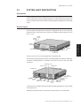
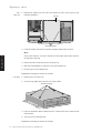
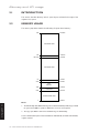
The system unit contains: the system board, drives, power supply and up to three
expansion cards.
Contents
Introduction
All the interface circuitry is on the system board.
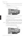
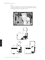
A block diagram of the system unit is shown at the end of this section. It shows the
components of the system and the functions implemented on the system board.
System board
Processor
The XEN can be fitted with any i486 processor with external clock speeds between
16 and 33 MHz.
Note
A processor upgrade socket is provided on the system board. The socket can be
configured to suit a wide range of Intel processors.
Some models are fitted with a 256 Kbyte external cache to further boost performance.
Memory
Ethernet interface The XEN system board may be fitted with an Ethernet interface.
An Intel 82596 Ethernet coprocessor forms the basis of this interface. The 82596 is a
high performance component which uses the processor’s local bus to maximise the
throughput of data to and from the network.
The XEN system board may be fitted with the Apricot Professional Audio subsystem.
This system includes a mixer, MIDI port and joystick, and is AdLib compatible.
Security
The XEN system board contains Apricot’s LOC Technology security sub-system
which, when used in conjunction with a KeyLOC card and LOC Technology software,
provides a sophisticated security system.
Chapter 5
Audio
Chapter 3
System memory can be expanded to a total of 64 Mbytes using two SIMM sockets on
the system board.
Chapter 3
Systems equipped with the on-board Ethernet interface have a minimum clock speed of
25MHz.
Chapter 2
1
The XEN system board is an extremely compact custom design using highly integrated
components. It utilizes carefully selected components to combine excellent performance
and reliability.
Chapter 6
XEN HARDWARE TECHNICAL REFERENCE 1/3
Contents
Introduction
Power supply
The XEN is fitted with a 145W power supply capable of powering a fully configured
system. The power supply can be set to operate from either a 240V or 110V AC mains
supply.
Drive bays
Two drive bays are incorporated in the system unit.
The 5.25" bay is in the centre of the system unit behind the door. This bay can hold one
standard half height 5.25" device. Apricot supplies a variety of floppy, tape and CDROM drives which may be fitted in this bay.
Keyboard
The keyboard is a full QWERTY typewriter keyboard and numeric keyboard together
with editing keys. The layout of the 102 key UK keyboard is compatible with the IBM
AT enhanced keyboard.
Any compatible keyboard can be plugged into the system unit.
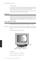
Monitors
The system board is fitted with a VGA video interface which will drive any suitable
monochrome or colour analogue monitor. Higher resolution video modes are also
supported. These require software specific display drivers and a suitable highresolution monitor.
The video output on the rear of the system unit may be connected to Apricot VGA
or HiVision monitors. Other manufacturers' VGA monitors may also be used.
Chapter 6
Chapter 5
Chapter 3
Chapter 3
Chapter 1
2
The 3.5" bay is at the front right of the system unit. The 3.5" floppy drive is mounted
on the top of the bay. One or two 1" high, or one 1.6" high, 3.5" hard disk drives may
be mounted in the bay.
1/4 XEN HARDWARE TECHNICAL REFERENCE
Expansion cards
The system unit provides three ISA expansion slots.
Contents
Introduction
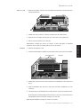
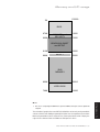
MONITOR
SERIAL
PORT
KEYBOARD
PORT
MOUSE
PORT
AUDIO
IN
AUDIO
OUT
EXPANSION
CARDS
THIN
THICK
TWISTED
ETHERNET ETHERNET
PAIR
PORT
PORT
ETHERNET
SYSTEM BOARD
INCLUDING
PROCESSOR: MEMORY:
VIDEO ADAPTER:
SYSTEM CONTROLLER:
UPGRADE SOCKET:
FLOPPY AND HARD DISK
CONTROLLERS:
SERIAL AND PARALLEL
PORTS: AUDIO SYSTEM:
INTEGRATED PERIPHERALS
CONTROLLER:
AC
AC
OULET INLET
POWER SUPPLY
CASELOCK
OPTIONS
ETHERNET INTERFACE:
SECONDARY CACHE:
LOC TECHNOLOGY:
AUDIO SYSTEM
3.5" DRIVEBAY
3.5"
E
Y DRIV
FLOPP
LOUDSPEAKER
Chapter 3
5.25" DRIVE BAY
Chapter 3
MIDI
PORT
VIDEO
PORT
Chapter 2
1
PARALLEL
PORT
LOUDSPEAKER
MOUSE
Chapter 5
FRONT BEZEL
KEYBOARD
Chapter 6
XEN HARDWARE TECHNICAL REFERENCE 1/5
SYSTEM UNIT
Chapter 2
Contents
2
SYSTEM UNIT
2.1 Introduction ............................2/2
Chapter 3
Chapter 5
XEN HARDWARE TECHNICAL REFERENCE 2/1
Chapter 2
3
2.5 System unit connectors ..2/33
VGA ....................................... 2/33
Serial port ............................. 2/33
Parallel port ......................... 2/34
Keyboard/mouse
connectors ........................... 2/34
Ethernet ................................ 2/35
Audio ..................................... 2/36
Chapter 2
2.3 Dismantling instructions .. 2/5
Servicing level ............................ 2/5
Warnings and cautions ............ 2/5
Anti-static precautions ............ 2/5
Equipment required ................. 2/5
System board connectors ....... 2/6
Dismantling and reassembly ... 2/7
Removing the top cover ..... 2/7
5.25" drive tray ..................... 2/8
5.25" drive .............................. 2/8
Expansion cards .................... 2/9
Backplane ................................ 2/9
Card guide support ............ 2/10
System board ....................... 2/10
3.5" drive bay ....................... 2/11
3.5" floppy drive .................. 2/12
3.5" hard disk drive ............ 2/13
Front bezel ........................... 2/13
PSU ........................................ 2/14
LED board ............................ 2/16
Loudspeakers....................... 2/16
System unit lock .................. 2/17
Side panels ............................ 2/17
Chapter 1
2.2 System unit description ....2/3
Construction ............................. 2/3
External layout .......................... 2/3
Internal layout ........................... 2/4
Power supply ......................... 2/4
3.5" drive bay ......................... 2/4
3.5" floppy drive .................... 2/4
5.25" drive tray ..................... 2/4
System board ......................... 2/4
2.4 Installing add-ons ...............2/18
Introduction ............................. 2/18
Expansion cards ...................... 2/18
Installation ............................ 2/18
Memory .................................... 2/20
Configurations ..................... 2/20
Installation ............................ 2/21
Processor upgrades ............... 2/22
Installation ............................ 2/25
Configuring the system
board ..................................... 2/26
5.25" drives .............................. 2/28
Generic ................................. 2/28
5.25" floppy or Irwin FTD 2/30
SLCD CD-ROM .................. 2/30
SCSI drives ........................... 2/31
3.5" hard disk drive ................ 2/31
Preparation .......................... 2/31
Drive configuration ............ 2/32
Installing the drive .............. 2/32
Contents
System unit
Contents
Chapter 1
2.1
INTRODUCTION
The main components of the system unit are:
•
chassis
•
top cover
•
front bezel
•
system board
•
power supply
The top cover is easily removed without any tools and allows access to all major
components.
The system board contains all the processing and interface circuitry and up to 64
Mbytes of system RAM. 4 Mbytes of RAM is soldered to the system board and SIMMs
can be fitted to increase the total amount of system RAM to 64 Mbytes.
Chapter 5
Chapter 3
2
Chapter 3
Chapter 2
System unit
2/2 XEN HARDWARE TECHNICAL REFERENCE
2.2
SYSTEM UNIT DESCRIPTION
Construction
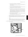
External layout
POWER
SWITCH
INFARED
SENSOR
LEDS
CASELOCK
LOUDSPEAKER
3.5" FLOPPY DRIVE
5.25" DRIVE BAY
LOUDSPEAKER
Chapter 2
3
VOLUME
CONTROL
Chapter 2
The front panel of the system unit contains: 3.5" floppy drive, door to 5.25" drive tray,
the power switch, the volume control, slots for three LEDs and the IR detector for the
KeyLOC card.
Chapter 1
A metal chassis and powder coated metal top cover form the basic structure to which
other components are attached. Separate plastic front bezel and side panels attach to
the front and either side of the chassis providing the distinctive appearance of the XEN
range.
Contents
System unit
The top cover lock is on the right hand side of the system unit.
EXPANSION SLOTS
SECURITY LOOP
THUMBSCREW
Chapter 3
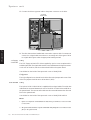
The rear panel of the system unit contains: serial and parallel ports, video port, Ethernet
connectors, blanking plates for expansion cards and AC power inlet and outlet
connectors.
THUMBSCREW
ETHERNET
CONNECTORS VIDEO
PORT
SERIAL
PORT PARALLEL
PORT
MOUSE
CONNECTOR
KEYBOARD
CONNECTOR
Connectors for the keyboard and mouse and the audio subsystem are on the left side
of the system unit.
Illustrations and pinouts of the connectors are given at the rear of this section.
XEN HARDWARE TECHNICAL REFERENCE 2/3
Chapter 5
POWER
POWER
IN
OUT
AUDIO
CONNECTORS
MIDI PORT
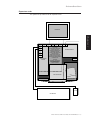
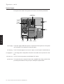
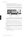
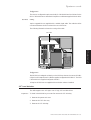
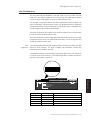
Internal layout
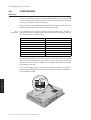
The layout of the inside of the system unit is shown in the following illustration.
Chapter 1
Contents
System unit
PROCESSOR
UPGRADE SOCKET
BLANKING
PLATES
POWER
SUPPLY
Chapter 2
EXPANSION
CARD
CONNECTORS
Chapter 5
Chapter 3
2
Chapter 3
3.5"
DRIVE BAY
CARD
GUIDES
BRACE
SIMM
SOCKETS
5.25"
DRIVE BAY
Power supply
The power supply satisfies all the power requirements of the system unit. The system
unit cooling fan is incorporated in the power supply.
3.5" drive bay
The 3.5" drive bay supports one or two 1" high, or one 1.6" high, 3.5" hard disk drives.
3.5" floppy drive
A 3.5" floppy drive is always fitted. The drive is mounted to the top of the 3.5" drive
bay.
5.25" drive tray
System board
The 5.25" drive tray supports one half height 5.25" device.
The system board is a high performance ISA compatible board that provides all the
processing and interface circuitry and up to 64 Mbytes of system RAM.
2/4 XEN HARDWARE TECHNICAL REFERENCE
2.3
DISMANTLING INSTRUCTIONS
Servicing level
Warnings and cautions
The XEN range has been designed to meet all international safety standards.
It is recommended that modifications are carried out by an authorized dealer.
Unqualified users should not normally dismantle the equipment.
•
Replacement parts should be of the type and rating specified by the manufacturer.
•
All earth connections must be maintained to the original specification.
•
Ensure that all personnel concerned are familiar with the action to be taken in
the event of electric shock.
Warning
Before removing any part of the system it must be powered down and disconnected from the
AC power supply.
All electronic components and equipments are sensitive to static electricity. Even small
electrostatic discharges can render components useless or severely shorten their
working life, therefore preventive measures should always be taken.
No work should be carried out on any item unless it is in a Special Handling Area (SHA)
as defined in BS CECC 00015:Part 1. In general this involves:
a common earth point
•
an earthed bench or bench mat
•
an earthed wrist strap
Equipment required
The following tools are required to dismantle the system unit.
•
Cross-head screwdriver
•
Flat bladed screwdriver
•
Nut spanner set
•
Pliers
XEN HARDWARE TECHNICAL REFERENCE 2/5
Chapter 5
•
Chapter 3
Anti-static precautions
Chapter 2
3
•
Chapter 2
To ensure safety and continued compliance with these standards, observe the following
precautions.
Chapter 1
The level of information in this section is intended to enable suitably qualified personnel
to remove and replace major components of the system unit, and access components
for option selection.
Contents
System unit
Contents
Chapter 1
System board connectors
Many of the dismantling/reassembly procedures that follow involve the disconnection
and reconnection of system board plugs and sockets. The following table gives, for each
socket, the connector number that identifies it. This number is printed on the system
board next to each connector.
Connector
Label
Hard disk drive
PL43
3.5" floppy disk drive
PL40
5.25" floppy disk drive
PL38
SLC CD-ROM
PL36
System board power
PL30
LED board
PL16
CD-ROM audio
PL4
Video disable jumper
PL50
VESA
PL21
ISA backplane
PL31
CMOS discharge
PL29
2
Chapter 3
Chapter 2
System unit
PL31
PL50
Chapter 5
Chapter 3
PL21
PL30
SW4
PL43
PL40
PL38
PL36
PL4
PL16
2/6 XEN HARDWARE TECHNICAL REFERENCE
SW1 PL29
Dismantling and reassembly
Removing the
top cover
1. Turn off both the system unit and the monitor.
Contents
System unit
2. If your AC power outlets have switches, set them to their Off positions.
4. Turn the caselock key to the unlocked position.
5. Loosen the two casing screws.
6. Slide the top cover rearwards slightly, then lift it off.
Chapter 1
3. Unplug all power cords from the rear of the system unit.
Chapter 2
CASELOCK
Chapter 2
3
CASING SCREW
CASING SCREW
Refitting the cover is the reverse of removal.
Four spring metal clips are fitted to the rear panel of the system unit and six to the front of
the top cover. They ensure good contact between the chassis and the cover and are necessary
for compliance with international RFI emission standards. If any of the clips is damaged during
removal or replacement of the top cover the system may no longer comply with these
regulations.
XEN HARDWARE TECHNICAL REFERENCE 2/7
Chapter 5
Note
Chapter 3
Take effective anti-static precautions while the top cover is off.
5.25"
drive tray
1. Remove the system unit top cover and identify the 5.25" drive tray from the
following illustration.
5.25" BAY
Chapter 2
Chapter 1
Contents
System unit
SECURING SCREWS
2. If a drive is fitted, disconnect the power and signal cables from the drive.
Note
2
Chapter 3
Some systems without a 5.25" drive may have the unused drive power cable secured to
the tray with a cable clip.
3. Remove the two screws that secure the drive tray.
4. Slide the tray backwards to clear the front of the system unit.
Replacement is simply the reverse of removal.
5.25" drive
1. Remove the 5.25" drive tray.
2. Turn the tray upside down and rest it on a flat surface.
SECURING SCREWS
Chapter 5
Chapter 3
5. Lift the tray out of the system unit.
T
COMPAC
3. From the illustration above, identify the four screws which secure the drive and
remove them.
4. The tray can now be lifted clear.
Replacement is simply the reverse of removal.
2/8 XEN HARDWARE TECHNICAL REFERENCE
Expansion cards
1. Remove the system unit top cover and identify the expansion card area from the
following illustration.
Contents
System unit
Chapter 1
3. Remove the screw which secures the rear of the card to the system unit.
4. Pull the card horizontally out of the slot.
Backplane
1. Remove all expansion cards.
2. Unclip the white plastic air baffle from the system unit brace and remove the baffle.
SECURING SCREWS
AIR BAFFLE
Chapter 2
3
Replacement is simply the reverse of removal. A fuller description of installing
expansion cards is given in Installing add-ons later in this section.
Chapter 2
2. Identify the card you wish to remove, and disconnect all cables from it.
Chapter 3
4. Align the backplane with the slot in the brace and lift the backplane out of its
connector.
5. Tilt the bottom of the backplane to the left and lower it down through the brace.
With the bottom of the backplane to the left of the connector on the system board
the backplane can be lowered far enough to be removed.
Replacing the backplane is simply the reverse of removal.
XEN HARDWARE TECHNICAL REFERENCE 2/9
Chapter 5
3. Identify and remove the two screws that secure the backplane to the system unit
brace.
Card guide
support
The card guide support at the front of the expansion card slots is secured to the base
of the system unit by two screws. To remove the card guide support:
1. Remove all expansion cards.
2. Remove the screw (or screws) that secure the card guide support to the base of
the system unit.
Chapter 1
Contents
System unit
Chapter 3
2
Chapter 3
Chapter 2
SECURING SCREWS
3. Lift the card guide support to free it from the locating lug at the front left of the
system unit and remove it from the system unit.
Replacement is simply the reverse of removal.
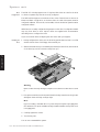
System board
1. In order to remove the system board you must first remove the: 5.25" drive tray,
expansion cards and backplane.
2. Disconnect all system board cables.
3. Remove the nine screws that secure the system board.
Chapter 5
intel
SECURING
SCREWS
i
DX
486
TM
SECURING
SCREWS
4. Remove the screwlocks on the ports on the rear of the system unit.
2/10 XEN HARDWARE TECHNICAL REFERENCE
5. If the system board is equipped with on-board Ethernet:
remove the two screws that secure the thick Ethernet connector slidelock, and
remove the slidelock
Contents
System unit
remove the nut that secures the thin Ethernet connector.
7. The system board can now be removed. In order for the connectors on the rear
left edges of the board to clear the chassis the board must move forward and right.
8. Once the connectors are clear of the chassis carefully pick the board up by its edges
and move it sideways out of the chassis.
9. Put the system board down on a suitable antistatic surface.
Note
3.5" drive bay
The 3.5" drive bay is secured to the base of the system unit by two screws and two lugs.
To remove the bay:
Chapter 5
intel
i
DX
486
Chapter 3
If the system board being inserted is a replacement make sure that the audio escutcheon plate
is fitted to the new board before you install it. The plate is secured by a screw and nut at the
left rear corner of the board, the screw must be inserted from beneath the board.
Chapter 2
3
Replacing the system board is simply the reverse of removal. Care should be taken
when replacing the board in the system unit, do not force the board into position, it
should move into position easily. If it does not, remove the board and try again.
Chapter 2
To remove the system board, carefully hold the front corners of the board between
thumb and forefinger, taking care to avoid touching any components. Then gently
move the front of the board to the right towards the 3.5" drive bay, and pull the
board towards the front of the system unit.
Chapter 1
6. If the system board is fitted with Apricot Professional Audio remove the screwlocks
on the MIDI connector on the left side of the system unit.
TM
SECURING
SCREWS
XEN HARDWARE TECHNICAL REFERENCE 2/11
1. Remove the top cover and the 5.25" drive tray.
2. Disconnect the power cables from any hard disk drives in the 3.5" drive bay.
3. Disconnect the drive signal cables at the system board.
4. Identify and remove the two screws that secure the drive bay.
5. Slide the drive bay backwards to free it from the lugs in the base of the system unit.
6. Lift the drive bay out of the system unit and place it on a suitable antistatic surface.
Replacement is simply the reverse of removal, however you must make sure that the
3.5" floppy drive signal cable is connected to the correct connector on the system
board, refer to the label on the inside of the top cover.
3.5" floppy drive
The 3.5" floppy drive is secured to the top of the 3.5" drive bay by three screws. To
remove the floppy drive:
1. Remove the 3.5" drive bay.
2. Carefully place the bay upside down on a suitable antistatic surface.
2
Chapter 3
Chapter 2
Chapter 1
Contents
System unit
Chapter 5
Chapter 3
SECURING SCREWS
3. Remove the three screws that secure the 3.5" floppy drive.
4. Lift the drive bay off the floppy drive.
Replacement is simply the reverse of removal. If the drive being installed is a
replacement you must ensure that the drive select switch is in the same position as the
old drive.
Warning
Make sure you use screws of the correct length. If you use longer screws you may do irreparable
damage to the drive.
2/12 XEN HARDWARE TECHNICAL REFERENCE
3.5" hard disk
drive
The 3.5" hard disk drives are secured to the 3.5" drive bay by four screws, two in each
side. To remove a hard disk drive:
1. Remove the 3.5" drive bay.
Contents
System unit
2. Carefully place the bay upside down on a suitable antistatic surface.
Chapter 1
3. Remove the four screws that secure the drive.
Chapter 2
Replacement is simply the reverse of removal. If the drive being installed is a
replacement you must ensure that the jumpers on the drive are correctly configured.
Two variants of the front bezel have been used in the XEN range. Initial shipments were
with a bezel which was secured by clips and double-sided tape, later units use a bezel
secured by clips and two screws. To remove the front bezel:
1. Remove the top cover and any expansion cards.
CLIPS
SCREW
XEN HARDWARE TECHNICAL REFERENCE 2/13
Chapter 5
2. Identify the clips, and whether the bezel is secured by screws. The clips and screws
are located inside the system unit. The clips are on either side of the 5.25" drive tray
and the screws are at either end of the front panel.
Chapter 3
Front bezel
Chapter 2
3
4. Slide the drive out of the bay.
3. If the bezel is secured by screws, remove the screws.
4. Using a flat-bladed screwdriver, free each of the clips in turn, and ease the top of
the bezel away from the system unit until there is a gap wide enough to get your
thumb and forefinger between the bezel and the front of the system unit.
Chapter 1
Contents
System unit
2
Chapter 3
Chapter 2
On systems where the bezel is secured using double sided tape applying pressure
with your thumbs to either end of the top edge of the bezel will help free the bezel
from the tape. The tape will remain on the top of the front of the system unit chassis.
Chapter 5
Chapter 3
5. The volume control switch on the left side of the bezel is connected, by a membrane
cable, to an LED board inside the front of the system unit. Identify the cable, then
reach between the bezel and the system unit and carefully disconnect it from the
system unit.
6. Rotate the bezel forward to an angle of approximately 45° to free the two clips at
the bottom of the bezel from the system unit, and lift the bezel away.
Replacing the front bezel is simply the reverse of removal, but you must be very careful
when reconnecting the volume control switch cable and rotating the bezel back into
position.
Make sure that the volume control switch connector is correctly plugged in to the LED
board. As you rotate the bezel back into position ensure that the cable passes through
the slot in the rear of bezel, and does not get trapped between the bezel and the front
of the system unit.
PSU
The XEN power supply is secured by four screws in the rear of the system unit and
two inside the system unit.
1. To remove the power supply you must first remove the 5.25" drive tray, the card
guide support and the front bezel.
2/14 XEN HARDWARE TECHNICAL REFERENCE
2. Remove the screw that secures the earth lead to the system unit base.
EARTH LEAD
Contents
System unit
Chapter 1
4. Remove the switch, and free the cable from the channel behind the 5.25" drive bay
aperture.
6. Remove the six screws that secure the power supply.
SECURING SCREWS
Chapter 2
3
5. Disconnect the system board and hard disk drive power cables.
Chapter 2
3. Remove the two screws that secure the system unit power switch to the front of
the system unit.
Chapter 3
Replacement is simply the reverse of removal. If the PSU you are installing is a
replacement and the old PSU on/off switch is fitted with a plastic case, you may have
to remove the plastic case from the old on/off switch and attach it to the new switch.
Warning
You must remember to reconnect the PSU earth lead to the chassis.
Ensure that the system meets the following electrical safety tests:
Earth bond resistance <0.1ohm excluding mains lead resistance
Earth leakage current <3.5mA total
Insulation resistance >2Mohms @ 500Vdc
Dielectric strength 2.2kV for 6 seconds
XEN HARDWARE TECHNICAL REFERENCE 2/15
Chapter 5
7. Remove the power supply.
LED board
The LED board is secured to the front of the chassis by two screws. To remove the
LED board:
1. To remove the power supply you must first remove the 5.25" drive tray and the
card guide support.
Chapter 1
Contents
System unit
2. Remove the two screws that secure the LED board.
Chapter 5
Chapter 3
2
Chapter 3
Chapter 2
SECURING SCREWS
3. Carefully move the LED board backwards taking care not to knock any of the LEDs
against the chassis.
4. Disconnect the loudspeaker cables and the cable to the system board.
5. Lift the LED board out of the system unit.
Replacement is simply the reverse of removal. Text on the rear of the LED board,
behind the loudspeaker connectors, indicates which loudspeaker should be plugged
into each connector. Systems with one loudspeaker use the left channel as viewed
from the front.
Loudspeakers
The XEN system unit provides mountings for two loudspeakers, one at each end of the
front of the system unit. The left loudspeaker is mounted in front of the card guide
support, the right one in front of the 3.5" drive bay. To remove the loudspeakers:
1. Remove the 3.5" drive bay and the card guide support.
2. Disconnect the loudspeaker cables from the LED board.
SECURING SCREWS
2/16 XEN HARDWARE TECHNICAL REFERENCE
3. Remove the screw (or screws) that secure the top of each loudspeaker.
4. Lift the loudspeakers out of the system unit.
The system unit lock is secured by a clip. To remove the lock simply pull the clip up
with a pair of pliers.
Side panels
The plastic panels along the bottom of each side of the system unit are not intended
to be removed. Under normal circumstances there should be no reason to remove
them.
Chapter 2
System unit lock
Chapter 1
Replacement is simply the reverse of removal. Text on the rear of the LED board,
behind the loudspeaker connectors, indicates which loudspeaker should be plugged
into each connector. Systems with one loudspeaker use the left channel as viewed
from the front.
Contents
System unit
Chapter 2
3
Chapter 3
The panels are each secured by four clips and can be removed by pushing the front of
the four clips outwards with a small screwdriver and sliding the panel backwards. In
order to remove the right panel you must first remove the system unit lock.
Chapter 5
XEN HARDWARE TECHNICAL REFERENCE 2/17
2.4
INSTALLING ADD-ONS
Introduction
This section contains instructions on installing add-ons and upgrades in the XEN range.
The areas covered include:
Chapter 5
Chapter 3
2
Chapter 3
Chapter 2
Chapter 1
Contents
System unit
•
expansion cards
•
additional memory
•
processor upgrades
•
additional drives
While you are installing add-ons you must take effective anti-static precautions as
described earlier in this section.
Expansion cards
Installation
The XEN provides three slots for the installation of ISA compatible expansion cards.
Installation of an expansion card in the XEN is a simple process requiring the removal
of only the system unit cover and a blanking plate. The following instructions and
illustrations describe how to install a card.
1. Remove the system unit cover.
2. With the system unit cover removed, the space for expansion cards will be visible.
It is on the left side of the system unit behind the activity indicators and the volume
control. Use the illustration below to help you identify this area.
PROCESSOR
UPGRADE SOCKET
BLANKING
PLATES
POWER
SUPPLY
EXPANSION
CARD
CONNECTORS
3.5"
DRIVE BAY
CARD
GUIDES
BRACE
2/18 XEN HARDWARE TECHNICAL REFERENCE
SIMM
SOCKETS
5.25"
DRIVE BAY
At the rear of the area are three metal blanking plates, one for each expansion card
slot. These plates cover slots in the rear of the system unit which will be used by
expansion cards.
3. The blanking plates are each secured by a screw. Decide which of the available slots
you wish to install the card in, then remove the appropriate blanking plate.
Warning
The video feature connector on the Revision D XEN system board uses a non-standard
pinout. In order to use this connector you need to make up a special cable.
To remove the blanking plate, first unscrew the securing screw, then slide the plate
out of its slot. Keep the screw, you will use it later to secure the card.
4. Before you install the card ensure that the card is correctly configured for your
system. Refer to appendix D for configuration information.
Note
6. Slide the card into the slot ensuring that the card edge connector engages correctly
with the backplane.
XEN HARDWARE TECHNICAL REFERENCE 2/19
Chapter 5
If the card uses the video feature connector on the system board, you must plug the video
feature cable into the system board socket before you install the card.
Chapter 3
5. Position the expansion card alongside the slot in which you wish to install it. Align
the rear of the card with the slot in the rear of the system unit, and, if the card is
full length, the front of the card with the card guide.
Chapter 2
3
Information on identifying the revision of the system board, and a pin out of the
video feature connector are given in Appendix B.
Chapter 2
In general it is easiest to start with the lowest slot and work towards the top, but
there a couple of exceptions. If you are installing a card which uses the video feature
connector on the system board then it is best to install the card in the lowest slot.
If you are installing a drive controller card that you want to connect to a drive in
the 5.25" drive tray then it is easiest to install it in the top slot.
Chapter 1
At the front of the area are three guides. These ensure that the front edge of any
full length card is secured.
Contents
System unit
Contents
System unit
7. Carefully push the card fully home. Do not apply excessive pressure.
8. Secure the card by replacing the screw that you removed in step 4.
Note
If you have installed a video display adapter that is CGA, EGA or VGA compatible you must
disable the system board video adapter by removing a jumper. If you do not remove this
jumper it is unlikely that either the video card or system board video adapter will operate
correctly.
The jumper is identified in the illustration on page 2/6. If you have a revision D
system board there is no video disable jumper. Refer to Appendix B for further
information.
10. Replace the system unit cover.
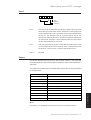
Memory
Configurations
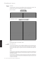
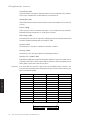
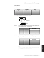
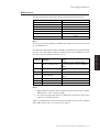
The XEN system board is fitted with 4 Mbytes of on-board memory, and sockets for
two SIMMs (Single In-line Memory Modules). Each socket can be empty, or fitted with
a SIMM of 4Mbyte (1Mx36), 8Mbyte (2Mx36), 16Mbyte (4Mx36) or 32Mbyte capacity.
The table below identifies the possible memory capacities using the various SIMM
combinations.
MM1
capacity
MM2
capacity
Chapter 5
Chapter 3
2
Chapter 3
Chapter 2
Chapter 1
9. Connect any signal cables to the card.
Upgrade
capacity
System
board
memory
Available
memory
-
-
-
4
4
4
-
4
4
8
8
-
8
4
12
16
-
16
4
20
32
-
32
4
36
4
4
8
4
12
4
8
12
4
16
4
16
20
4
24
8
8
16
4
20
8
16
24
4
28
16
16
32
4
36
32
4
36
4
40
32
8
40
4
44
32
16
48
4
52
32
32
64
4
64
Note
When a 32Mbyte SIMM is installed in MM2 the system board memory is disabled.
It should be noted that, for all combinations the SIMM in MM1 can be swapped with
that in MM2. In every case the computer will operate correctly when it is powered up,
and in most cases there will be no difference in the operation of the computer.
2/20 XEN HARDWARE TECHNICAL REFERENCE
There are only two exceptions to this. In the two situations given below, although the
computer will operate if the SIMMs are swapped it is preferable if the SIMMS are
installed as described.
If you are upgrading to 24 Mbytes of system memory, i.e. you have one 4 and one
16 Mbyte SIMM, the 4 Mbyte SIMM should always be installed in MM1.
•
If you are installing a 32Mbyte SIMM it should always go in MM1 unless there is
a 32Mbyte SIMM in the socket already.
If in either of the cases above you install a 4 or 32 Mbyte in MM2 when you power the
system up you will be prompted to swap the SIMMs.
In order to install a memory upgrade you must remove the system unit cover and the
5.25" drive tray.
Removing a SIMM
If you wish to install an upgrade in a SIMM socket which is already occupied you must
first remove the existing SIMM.
2. Place your thumbs on the top edge of the SIMM and move it gently towards the
vertical.
Chapter 2
3
1. Lever the metal clips on each side of the socket gently away from the SIMM using
your forefingers.
Chapter 2
Installation
Chapter 1
•
Contents
System unit
Chapter 3
Inserting a SIMM
From the table of possible SIMM combinations decide which SIMM capacity will be
installed in the socket. Then install the SIMM.
To fit a SIMM:
1. The SIMM will only install in one orientation. There is a cutout at one end of the
SIMM next to the connector strip.
Hold the SIMM with the cutout on the right and metal connector strip nearest the
system board.
XEN HARDWARE TECHNICAL REFERENCE 2/21
Chapter 5
3. When the SIMM has rotated through 20°, taking care to avoid touching any of the
components on the SIMM, grip the top corners of the SIMM between thumb and
first finger and carefully pull the SIMM out of the socket.
2. Position the SIMM above the socket with the SIMM tilted slightly towards the front
of the system unit.
Chapter 5
Chapter 3
2
Chapter 3
Chapter 2
Chapter 1
Contents
System unit
3. Lower the SIMM into the socket, and ensure that the SIMM is properly located in
the connector.
4. Pushing gently on the top corners rotate the SIMM towards the horizontal until it
clips into place. Do not use excessive force.
If the SIMM will not rotate easily remove it and start again.
5. If the SIMM is properly located the SIMM should remain in position held by the
securing clips, and with a small plastic lug through the holes on either side of the
SIMM.
If you want to install a second SIMM repeat the process above. Once you have
completed installation you can replace the 5.25" drive tray and reassemble the system.
The next time you power the system up the SETUP utility will be invoked automatically.
Processor upgrades
The XEN system board is fitted with a processor socket that supports any Intel486SX,
Intel487SX, Intel486DX, Intel486DX2 or OverDrive processor with a maximum
external clock speed of 33MHz.
Any other Intel processor using the same pinout as one of these processors could also
be installed, subject to the same 33MHz maximum external clock speed restriction.
2/22 XEN HARDWARE TECHNICAL REFERENCE
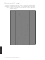
The table below lists the possible upgrades for each processor type and speed.
Current Processor
Speed
Intel486SX
25
33
Intel486DX
33
Speed
Intel487SX
25
Intel487SX
33
OverDrive
25
OverDrive
33
Intel487SX
33
OverDrive
25
OverDrive
33
OverDrive
25
OverDrive
33
This table lists the processors supported by the system board. There is no guarantee that any
particular upgrade processor will be available at any given time.
1. Remove the system unit cover.
2. Identify the processor upgrade socket.
OCCUPIED SOCKET
intel
OVERDR IVE
Chapter 3
UNOCCUPIED SOCKET
Chapter 2
3
Depending on the processor type fitted in your system unit the processor socket may
already be occupied. Before installing the upgrade processor you must first check
whether the processor socket is occupied, and if it is, remove the existing processor.
Instructions on locating the socket and removing a processor are given below.
Chapter 2
Note
Chapter 1
Intel486SX
Upgrade Processor
Contents
System unit
Chapter 5
If the socket is occupied you will have to remove the processor before you can
install the upgrade processor.
XEN HARDWARE TECHNICAL REFERENCE 2/23
3. Your upgrade processor is supplied with an extraction tool which resembles a
miniature garden rake.
4. Carefully insert the prongs of the extractor between the bottom of the processor
and its socket. You may need to twist the extractor gently from side to side to work
the prongs into place.
Chapter 5
Chapter 3
2
Chapter 3
Chapter 2
Chapter 1
Contents
System unit
Be careful to ensure that the prongs do not go between the system board and the
socket.
5. Ease the processor up slightly by pushing inwards on the extractor’s handle.
Warning
Do not push hard on the handle. The processor must be removed gradually and evenly by
working the tool under each edge in turn. Attempting to lift one edge of the processor too
far will damage the processor, or the socket, or both.
6. Remove the extractor and repeat the process on each edge of the processor,
gradually easing the processor out of its socket. If necessary work your way round
the processor two or three times.
7. Once the processor is free of its socket lift it out of the system unit and place it on
the anti-static foam provided with the upgrade processor.
2/24 XEN HARDWARE TECHNICAL REFERENCE
Installation
Having identified the upgrade socket, and ensured that it does not have a processor in
it you are ready to install your new upgrade processor.
1. The upgrade processor and socket are keyed to ensure that the processor can only
be installed in one orientation.
intel
Chapter 1
The inside of one corner of the socket has a key hole, the outside of the same corner
is missing three holes. The processor has a positioning guide in the form of a small
dot of paint. Use the following illustration to help identify these features.
Contents
System unit
OVERDR IVE
KEYED
CORNER
PROCESSOR
IN CENTRE
intel
OVERDR IVE
Warning
If the processor is misaligned it will not go into the socket, and any attempt to force it will
damage the processor, or the socket, or both.
XEN HARDWARE TECHNICAL REFERENCE 2/25
Chapter 5
UNOCCUPIED
HOLES ON
EACH SIDE
Chapter 3
If the upgrade processor does not occupy all four rows of holes it should be
positioned centrally as shown below.
Chapter 2
3
2. Carefully position the upgrade processor above the socket with the positioning
guide on the processor over the keyed corner of the socket.
Chapter 2
POSITIONING
GUIDE
3. Gently insert the upgrade processor making sure that it is correctly aligned with the
socket and that you do not bend or otherwise damage the pins.
4. Once you are certain that all the pins on the processor are in the holes in the socket
apply firm even pressure to the top of the processor to seat the pins in the socket.
5. With the upgrade processor installed you must now ensure that the upgrade
socket, and system board clock speed are correctly configured for your new
processor.
Configuring the system board below describes how to ensure that when you
reassemble your system the new processor will work.
Configuring the
system board
The XEN system board supports a range of processor speeds and the upgrade socket
supports a range of processor types. The system board clock speed and the upgrade
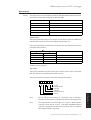
socket are configured using four switches in a set of six by the socket.
It is vital that both the system clock speed, and the upgrade socket configuration are
set correctly. Follow the instructions below to check the settings and adjust them as
necessary.
4
5
6
1. Use the following illustration to identify the switches.
Chapter 5
1
ON
2
3
Chapter 3
2
Chapter 3
Chapter 2
Chapter 1
Contents
System unit
intel
OVERDR IVE
SWITCH PACK
The switches numbered 2 and 3 are used to select the system clock speed. Switches
4 and 5 are used to configure the upgrade socket.
Warning
Under no circumstances should switches 1 and 6 of the switch pack be moved. It is essential
that both switch 1 and switch 6 are in the on position.
2/26 XEN HARDWARE TECHNICAL REFERENCE
2. From the table below, and the label on your upgrade processor or its packaging,
decide which processor type you have installed.
Switch
4
5
off
off
Processor
Intel487SX/OverDrive
on
Intel486DX/Intel486DX2
off
Intel486SX
on
on
not used
3. Having decided which selection you require check the positions of switches 4 and
5, and if necessary move them to the appropriate position.
4. From the table below, and the label on your upgrade processor, or its packaging
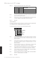
decide which system clock speed you need to select.
2
3
Clock speed
(MHz)
on
on
16
on
off
20
off
on
25
off
off
33
Note
Systems equipped with the on-board Ethernet interface have a minimum clock speed of
25MHz.
If you have installed an OverDrive processor you should set the system clock speed
to match the external interface speed of the processor. OverDrive processors use
Intel’s clock doubling technology and the processor runs at twice the speed of its
interface to the system board.
The labelling on the OverDrive processor or its packaging should make it clear what
its external interface speed is.
5. Having decided which selection you require check the positions of switches 2 and
3, and if necessary move them to the appropriate position.
6. Once you are satisfied that you have installed the upgrade and configured the
system correctly, reassemble the system.
XEN HARDWARE TECHNICAL REFERENCE 2/27
Chapter 5
If you have installed an Intel487SX you must set the system clock speed to match
the speed of the coprocessor.
Chapter 3
You will almost certainly want to set the clock speed to either 25 or 33MHz.
Chapter 2
3
Switch
Chapter 2
off
on
Chapter 1
Since the Intel487SX and OverDrive processors require the same configuration
you will normally set switches 4 and 5 to the Off/Off position. The other selections
are for processors normally installed during manufacture.
Contents
System unit
Contents
Chapter 1
System unit
5.25" drives
The 5.25" drive tray in the XEN system unit can contain any half height 5.25" device.
Apricot supplies a range of tape and CD-ROM drives, and a 5.25" floppy drive, for this
tray.
The following instructions describe the installation of a drive in the tray. The Generic
instructions apply to all drives, and describe the physical installation of a drive.
Instructions specific to each drive type are given after the generic instructions.
Generic
1. Remove the system unit cover.
SECURING SCREWS
2. Remove the drive tray as described in the dismantling instructions earlier in this
section.
3. The front of the tray may be fitted with a blanking plate. If it is, turn the tray over
and remove the two screws that secure the blanking plate. The blanking plate is no
longer required, but you may wish to store it somewhere safe in case you wish to
remove the drive later.
SECURING SCREWS
Chapter 5
Chapter 3
2
Chapter 3
Chapter 2
5.25" BAY
BLANKING PLATE
If the drive tray is not fitted with a blanking plate, the 5.25" drive aperture is
obscured by a blanking plate attached to the top of the front of the chassis, behind
the drive bay door. Break this blanking plate out by bending it backwards and
returning it to the vertical position several times.
4. Remove the drive from its packaging. With the drive there should be four screws
and a signal cable. Some drives may be supplied with additional items.
2/28 XEN HARDWARE TECHNICAL REFERENCE
5. If necessary configure the drive. Drives supplied by Apricot will be correctly
configured for installation in a XEN.
For information on how Apricot-supplied drives are configured see the drive
specific information following these installation instructions.
7. Rest the drive, top down, on a suitable anti-static surface.
8. With the drive tray upside-down place it over the drive. The front of the drive must
be at the end where the blanking plate was fitted.
Chapter 2
9. Line up the holes in the underside of the drive with those in the base of the drive
tray.
Chapter 1
6. Identify the top and bottom of the drive.
Contents
System unit
Chapter 2
3
SECURING
SCREW
HOLES
11. Gently tighten the four screws.
12. Replace the drive tray.
XEN HARDWARE TECHNICAL REFERENCE 2/29
Chapter 5
10. Insert the four drive securing screws, and tighten them until they are finger tight.
Chapter 3
T
COMPAC
13. Connect the drive tray power cable to the power connector on the drive.
5.25" DRIVE
POWER CABLE
Chapter 1
Contents
System unit
intel
14. The drive has now been installed and connected to a power cable. You must now
connect it to a signal cable. Instructions on connecting each of the types of drive
to a signal cable is given under the appropriate heading overleaf.
5.25" floppy
or Irwin FTD
Chapter 5
Cabling
The 5.25" floppy and Irwin FTD drives supplied by Apricot come complete with a
suitable signal cable. The signal cable must be connected between the signal connector
on the rear of the drive, and the socket marked PL38 on the system board.
Chapter 3
2
Chapter 3
Chapter 2
OVERDR IVE
Use the label on the inside of the system unit cover to identify PL38.
Configuration
The only configuration on these drives is via the drive select jumpers at the rear of the
drive. The jumpers should be set to drive select 1 (DS1).
SLCD CD-ROM
Cabling
The Apricot SLCD CD-ROM drive is supplied with two signal cables. The wide data
cable must be connected between the rear of the SLCD CD-ROM drive and PL36 on
the system board. The narrow audio cable must be connected between the drive and
PL4 on the system board.
Use the label on the inside of the system unit cover to identify PL36 and PL4.
Notes
1. If there is an expansion card installed in the bottom slot you will have to remove it in order
to access PL4.
2. On system boards which have only the standard PC audio facility there is no audio connector
(PL4) on the system board.
2/30 XEN HARDWARE TECHNICAL REFERENCE
Configuration
There are no configuration options on the SLCD CD-ROM drives. DOS drivers for the
SLCD CD-ROM drive are described in help files on a diskette supplied with the drive.
SCSI drives
Contents
System unit
Cabling
The following illustration shows the routing of the cable.
SCSI CABLE
DX
486
TM
Chapter 2
intel
i
Chapter 1
Apricot upgrade kits are supplied with a suitable signal cable. The cable should be
connected between the SCSI card and the rear of the drive.
Chapter 2
3
All Apricot SCSI drives are supplied with termination resistors installed.
3.5" hard disk drive
The XEN supports one 1.6" high or two 1" high, 3.5" hard disk drives.
Preparation
To install a hard disk drive you must first remove the 3.5" drive bay:
1. Remove the system unit cover.
2. Remove the 5.25" drive tray
3. Remove the 3.5" drive bay.
XEN HARDWARE TECHNICAL REFERENCE 2/31
Chapter 5
Each SCSI drive is assigned an identity on the SCSI bus, these are known as SCSI IDs.
All Apricot SCSI tape drives for XEN are supplied configured with SCSI ID 2. The SCSI
CD-ROM drive is supplied configured with ID 5.
Chapter 3
Configuration
Drive
configuration
IDE drives are normally configured using jumpers on the drive. Configuration details
may vary from drive to drive. Apricot drives are supplied with documentation
describing how to configure the drive.
If you are uncertain about configuring the drive check with your supplier.
Installing the
drive
1. Having configured the drive, turn the drive bay upside-down and rest it on a flat
surface with the front of the floppy drive towards you.
2. Slide the hard disk drive you are installing into the bay from the front, with the drive
circuit board up, and its connectors away from you.
Chapter 3
2
Chapter 3
Chapter 2
The XEN 3.5" drive bay supports two 1" high hard disk drives. In order for the drive
or drives to operate they must be correctly configured.
The IDE interface supports a maximum of two drives. These drives are known as
Master and Slave. A single drive, or the boot device in a dual drive system, must be
configured as Master. The second, non-bootable, drive in a dual drive system must be
configured as Slave.
Chapter 1
Contents
System unit
Chapter 5
Warning
If there is a drive in the bay already, be careful to ensure that the new drive does not touch
it.
3. Line up the screw holes on the drive with those in the bay, insert the securing screws
and tighten them until they are finger tight.
Note
If you are installing a hard disk drive in a system that previously had only a floppy drive
there will be two sets of holes available in the bay. Install the hard drive in the position closer
to the floppy drive.
4. Carefully tighten the screws.
5. Turn the bay over.
You can now reassemble the system.
2/32 XEN HARDWARE TECHNICAL REFERENCE
2.5
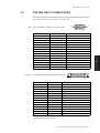
SYSTEM UNIT CONNECTORS
The following illustrations and tables show the layout, pin numbering and pinout of each
of the connectors on the rear panel of the system unit.
VGA
6
10
The VGA display connector is a 15-pin D-shell.
15
Output
1
O
Red
2
O
Green
3
O
Blue
4
NA
Reserved
5
NA
Digital Gnd
6
NA
Red rtn
7
NA
Green rtn
8
NA
Blue rtn
9
NA
Plug
10
NA
Digital Gnd
11
NA
Reserved
12
NA
13
O
Hsync
14
O
Vsync
15
NA
Chapter 2
3
I/O
11
Chapter 2
Pin
Reserved
Reserved
1
13
The serial port uses a male 25-pin D-shell connector.
14
I/O
Signal name
2
O
Transmit data (COM1)
3
I
Receive data (COM1)
4
O
5
I
Clear to send (COM1)
6
I
Data set ready (COM1)
7
NA
Request to send (COM1)
Signal ground
8
I
Data carrier detect (COM1)
12
I
Data carrier detect (COM2)
13
I
Clear to send (COM2)
14
O
Transmit data (COM2)
16
I
Receive data (COM2)
19
O
Request to send (COM2)
20
O
Data terminal ready (COM1)
22
I
Ring indicate (COM1)
All other pins are not connected.
XEN HARDWARE TECHNICAL REFERENCE 2/33
Chapter 5
Pin
25
Chapter 3
Serial port
1
Chapter 1
5
Contents
System unit
Parallel port
Keyboard/mouse
connectors
13
1
25
14
The parallel port uses a female 25-pin D-shell
connector.
Pin
I/O
Signal name
Pin
I/O
Signal name
1
I/O
Strobe
14
O
Autofeed XT-
2
3
I/O
Data bit 0
15
I
I/O
Data bit 1
16
O
4
I/O
Data bit 2
17
O
Slct In-
5
I/O
Data bit 3
18
NA
Ground
ErrorInit-
6
I/O
Data bit 4
19
NA
Ground
7
I/O
Data bit 5
20
NA
Ground
8
I/O
Data bit 6
21
NA
Ground
9
I/O
Data bit 7
22
NA
Ground
10
I
Ack-
23
NA
Ground
11
I
Busy
24
NA
Ground
25
NA
Ground
12
I
PE
13
I
SLCT
The keyboard and mouse connectors are both miniature 6-pin
DIN connectors.
6
5
4
3
2
Pin
I/O
Signal name
1
I/O
Data
2
NA
Reserved
3
NA
Ground
4
NA
+5Vdc
5
I/O
Clock
6
NA
Reserved
Chapter 5
Chapter 3
2
Chapter 3
Chapter 2
Chapter 1
Contents
System unit
2/34 XEN HARDWARE TECHNICAL REFERENCE
1
Ethernet
Thick
8
1
15
9
The thick Ethernet connector is a 15-pin female D-shell which
uses a slide to hold the male and female connectors together.
I/O
Signal
1
NA
Collision presence shield
2
I
Collision presence (+ve)
3
O
Transmit (+ve)
4
NA
Receive shield
I
Receive (+ve)
NA
Power return
7
NA
Reserved (+ve)
8
NA
Reserved shield
9
I
Collision presence (-ve)
10
O
Transmit (-ve)
11
NA
Transmit shield
I
NA
Power
Receive (-ve)
14
NA
Power shield
15
NA
Reserved (-ve)
Thin
The thin Ethernet connector is a BNC socket.
Signal
Return
Twisted pair (TPE)
The unshielded twisted pair Ethernet port is an
RJ45 connector.
Function
1
Transmit data +
2
Transmit data -
3
Receive data +
4
Not used
5
Not used
6
Receive data -
7
Not used
8
Not used
XEN HARDWARE TECHNICAL REFERENCE 2/35
Chapter 5
Pin
123 4 5 6 78
Chapter 3
Core
Shield
Chapter 2
3
12
13
Chapter 2
5
6
Chapter 1
Pin
Contents
System unit
Contents
Chapter 1
Chapter 2
2
Chapter 3
Audio
Joystick/MIDI port
8
1
15
9
The Joystick/MIDI port connector is a 15-pin female
D-shell compatible with the port found on Sound Blaster cards.
Pin
I/O
Function
1
NA
+5V dc
2
I
GP4 Joystick/A right button
3
I
GP0 Joystick/A x-coordinate
4
NA
Ground
5
NA
Ground
6
I
GP1 Joystick/A y-coordinate
7
I
GP5 Joystick/A left button
8
NA
+5V dc
9
NA
+5V dc
10
I
GP6 Joystick/B right button
11
I
GP2 Joystick/B x-coordinate
12
O
13
I
GP3 Joystick/B y-coordinate
14
I
GP7 Joystick/B left button
15
I
MIDI In
MIDI Out
Audio input
The audio input connector is a standard 3.5mm socket. Input sensitivity is software
controllable to suit a range of devices from a microphone to hi-fi equipment line outputs
and personal stereo headphone outputs.
Audio output
The audio output connector is a standard 3.5mm stereo headphone socket.
Chapter 5
Chapter 3
System unit
2/36 XEN HARDWARE TECHNICAL REFERENCE
SYSTEM BOARD
Chapter 3
System board
Contents
3
SYSTEM BOARD
3.1 Introduction ............................3/2
General ....................................... 3/2
System Identification Number
(SIN) ........................................ 3/2
Major components ............... 3/2
Description ................................ 3/4
Processor upgrades .............. 3/5
System reset .......................... 3/5
3.5 Video controller ...................3/10
General ..................................... 3/10
Video controllers ................ 3/12
Video disable jumper ......... 3/12
3.6 Floppy disk controller ......3/12
3.12 Professional audio ..............3/22
General ..................................... 3/22
YMZ263 multimedia
controller ............................. 3/23
YMF262 FM synthesizer .... 3/23
LMC835 mixer .................... 3/23
CD-ROM audio .................. 3/23
Microphone/line input ....... 3/23
PC beep ................................ 3/23
LMC1982 volume/tone
control .................................. 3/23
Front panel volume control . 3/
23
Power amplifier ................... 3/23
3.13 System board
connectors ............................ 3/24
Hard disk drive connector ... 3/24
SLC interface connector ....... 3/24
Floppy drive connectors ....... 3/25
Audio data ................................ 3/25
System board power
connector ................................. 3/26
Front panel connector .......... 3/26
VESA connector ..................... 3/26
Battery jumper ........................ 3/27
XEN HARDWARE TECHNICAL REFERENCE 3/1
Chapter 5
3.7 Hard disk and SLC
interfaces ............................... 3/13
General ..................................... 3/13
Interface signal descriptions . 3/13
Host reset ............................ 3/13
Host data 0-15 .................... 3/13
Host I/O channel ready ..... 3/13
Host IOW ............................ 3/13
Host IOR .............................. 3/13
Host IRQ14 ......................... 3/13
Host IOCS16 ....................... 3/13
Host ADDR 0-2 .................. 3/13
Chip select 0, 1 ................... 3/13
3.11 Ethernet port .......................3/20
General ..................................... 3/20
82596 LAN coprocessor .. 3/21
82503 dual serial
transceiver ........................... 3/21
7997 ....................................... 3/21
1
Chapter
Contents3
3.4 System memory ...................3/9
General ....................................... 3/9
Read only memory (ROM) ..... 3/9
Random access memory
(RAM) ....................................... 3/10
3.10 LOC Technology ................3/20
Chapter 3
3.3 VL82C486 ................................3/6
Memory controller ............... 3/6
System control port B ......... 3/6
Interrupt structure ................... 3/6
List of hardware interrupts 3/7
Non-Maskable Interrupts.... 3/8
Direct Memory Access ........... 3/8
Address generation .............. 3/8
System timers ............................ 3/9
Operation ............................... 3/9
3.9 82C113A .................................3/15
Real time clock (RTC) RAM 3/15
Contents of RTC RAM ..... 3/15
Keyboard port ........................ 3/19
Keyboard password
security ................................. 3/20
Chapter 2
3.2 Processor system .................3/5
3.8 Peripherals controller ......3/14
Serial ports ............................... 3/14
Programmable baud-rate
generator .............................. 3/14
Parallel port ............................. 3/15
System board
3.1
INTRODUCTION
General
This section describes the XEN system board and the operation of its processing
system and interface circuits.
Chapter 5
Chapter
Contents3
1
Chapter 3
Chapter 2
The XEN range uses a highly integrated, IBM AT compatible system board. In addition
to standard features, the XEN system board can provide: Ethernet interface, business
or professional audio subsystem, LOC Technology security subsystem and a mouse
port.
Note
This section describes revision F of the XEN system board. The differences between revision
F and the earlier revisions of the system board are noted in this section, and described in
appendix B.
System
Identification
Number (SIN)
Each system board fitted with the LOC Technology subsystem is identified by
its own System Identification Number (SIN). During normal operation the SIN will
never be required. Under certain circumstances the system may display a prompt
asking for the SIN to be entered. If this happens refer to the Owners Handbook and
associated documentation.
If Apricot’s LOC Technology software is in use refer to the documentation supplied
with the software.
Major
components
The following list of components on the system board identifies the major chips
and briefly details their function:
1.
Processor:
i486 family
2.
4 Mbytes of RAM
3.
128 Kbyte ROM
4.
VL82C486 AT chipset
5.
CL-GD542X video controller
6.
ATA (IDE) compatible hard disk interface
7.
82077 based floppy drive interface
8.
16C452 based serial and parallel ports
9.
Two SIMM sockets for memory expansion (up to 64Mbytes)
10.
VL82C113A combination I/O chip
11.
Yamaha YMZ263 based professional audio subsystem (optional)
12.
8051 based LOC Technology security feature (optional)
13.
82596 based Ethernet interface (optional)
14.
SLC CD-ROM interface.
3/2 XEN HARDWARE TECHNICAL REFERENCE
System board
The major components are identified in the following illustration.
SERIAL/PARALLEL
PORT
VESA FEATURE
CONNECTOR
EXPANSION
ROM SOCKET BIOS ROM
SECURITY
PROCESSOR
PROCESSOR/
PROCESSOR
UPGRADE
SOCKET
AUDIO
INTERGRATED
PERIPHERALS
CONTROLLER
EXTERNAL
CACHE
RAM
EXTERNAL
CACHE
CONTROLLER
FLOPPY
CONTROLLER
QFP
PROCESSOR
SIMM SOCKET 2
1
Chapter
Contents3
SYSTEM
CONTROLLER
Chapter 3
ETHERNET
COPROCESSOR
Chapter 2
VIDEO
CONTROLLER
RAM
SIMM SOCKET 1
Note
The expansion ROM socket is never fitted to system boards without the on-board Ethernet
port. It may not be fitted to some system boards which are equipped with the on-board
Ethernet port.
XEN HARDWARE TECHNICAL REFERENCE 3/3
Chapter 5
BATTERY
System board
Description
SYSTEM ADDRESS
SYSTEM DATA
SYSTEM
RAM
MEMORY
ADDRESS
82C486
SYSTEM
CONTROLLER
LOCAL DATA
82C425
CACHE
CONTROLLER
AND RAM
UPGRADE
PROCESSOR
SOCKET
PROCESSOR
LOCAL ADDRESS
82C596
ETHERNET
COPROCESSOR
82C113A
COMBINATION
I/O
BIOS
ROM
VIDEO
CONTROLLER
Chapter 3
Chapter 5
Chapter
Contents3
1
HARD DISK
AND
SLC CD-ROM
INTERFACE
16C452
SERIAL
AND
PARALLEL
PORTS
Chapter 2
82077SL
FLOPPY
DISK
INTERFACE
AUDIO
SUBSYSTEM
ISA BUS
EXPANSION
CONNECTOR
The following description of the system board should be read in conjunction with the
block diagram below. The diagram shows the peripheral areas of circuitry which are
connected to the CPU. For clarity, timing and control signals are omitted.
The block diagram is a functional description of the system board and does not identify
specific chips. The XEN system board uses highly integrated components, reducing the
chip count and the system board area, and increasing reliability.
3/4 XEN HARDWARE TECHNICAL REFERENCE
System board
The VLSI 82C486 chipset integrates much of the standard AT system board peripheral
logic onto a single chip. The processor, processor upgrade socket, cache and Ethernet
coprocessor are connected to a 32-bit local bus. Control logic for the local bus is
integrated in the 82C486.
Memory addresses are generated by 82C486 and are routed to system memory on a
dedicated memory address bus. Memory data uses the local data bus.
The 82596 based Ethernet interface connects directly to the local bus allowing fast
transfers to and from system memory.
The 82C113A combination I/O chip is connected to the system address and data buses,
and the local address bus.
All other peripheral circuitry is connected to the system bus.
The system board includes a processor upgrade socket. This socket can be configured
for a wide variety of i486 family processors with an external clock speed of up to 33
MHz.
System reset
The system is automatically reset on power up. No external hardware reset facility is
provided. Some operating systems provide a software reset e.g. MS-DOS resets the
machine if CTRL, ALT and DEL are pressed at the same time.
3.2
PROCESSOR SYSTEM
The processor system uses an i486 microprocessor, these are described below.
Chapter 3
Processor
upgrades
Chapter 2
The BIOS ROM is addressed from the system bus and places its data on the local bus.
The Intel i486 is a high performance microprocessor which features:
•
compatibility with software written for less powerful members of the Intel
microprocessor family - the 8086, 8088, 80286 and 80386.
•
high speed
•
enhanced modes of operation - real, protected and virtual 8086 mode.
•
on board memory management unit.
•
on board implementation of 80387DX numeric coprocessor (not fitted on SX
variants).
•
on board cache controller and 8 kbyte cache RAM.
•
burst mode which allows the transfer of 16-bytes of data in 5 clock cycles.
•
multiprocessor support.
The XEN system board has two processor sites. One site is used during manufacture
to fit processors in Quad Flat Pack (QFP) packages. The second processor site is an
upgrade site which supports a wide variety of i486 processors.
Not all i486 family processors are available in QFP form, therefore for some processor
types the upgrade socket is occupied by the processor installed during manufacture.
The upgrade socket can still be used by removing the original processor.
XEN HARDWARE TECHNICAL REFERENCE 3/5
Chapter 5
32-bit address and data busses.
1
Chapter
Contents3
•
System board
3.3
VL82C486
Chapter 5
Chapter
Contents3
1
Chapter 3
Chapter 2
The XEN system board is based on a VLSI VL82C486 single chip AT compatible chipset.
The VL82C486 integrates the following standard AT system board peripheral logic in
a single QFP package:
•
two 8237A DMA controllers
•
two 82C59A interrupt controllers
•
82C54 system timer
•
74LS612 memory mapper (extended to support 64Mbyte of RAM)
•
82284 clock generator and ready interface
•
82288 bus controller
In addition to the logic listed above the VL82C486 also includes:
Memory
controller
•
memory controller
•
bus steering logic
•
parity generation and checking logic
•
Port B and NMI logic
•
interface to VL82C113A combination I/O chip.
The memory controller integrated in the VL82C486 can access 64 Mbyte of the
processor’s address range. Memory is addressed in up to four banks. Page mode
operation and interleaving maximise system performance.
An interface is provided for the VL82C425 cache controller. ROM shadowing is
supported from 640k to 1M.
System control
port B
Port B is located at I/O location 0061h. The port may be used for: gate timer 2 (speaker);
speaker data; RAM parity check enable; enable I/O channel check; refresh detect; timer
2 out; I/O channel check; RAM parity check.
Interrupt structure
The system board supports 16 levels of edge sensitive, maskable hardware interrupts,
including Non-Maskable Interrupts (NMI).
The interrupt control circuitry is functionally equivalent to two 8259A programmable
interrupt controllers. Each controller has eight interrupt inputs; one interrupt input is
used to cascade the controllers together. This leaves fifteen inputs available for the
processing system to use.
The output from the controllers goes to the INTR input on the processor. All of the
interrupts may be masked using the processor CLI instruction.
3/6 XEN HARDWARE TECHNICAL REFERENCE
System board
The following illustration shows the maskable interrupt structure.
IRQ0
IRQ1
0
INT
INTR
1
INTA
INTA
2
IRQ3
IRQ4
IRQ5
IRQ6
IRQ7
4
D0 to D7
XD0 to XD7
8-BIT
DATA
BUS
5
6
RD,WR
7
A0
MASTER
CONTROLLER
IOR, IOW
SA0 ADDRESS
BUS
INT
0
INTA
1
2
3
D0 to D7
4
RD,WR
5
A0
6
The interrupts are allocated to hardware functions in the priorities shown in the
following table. IRQ0 is the highest priority. Appendix D provides some additional
information.
Function
IRQ0
Timer
IRQ1
Keyboard
IRQ2
Slave controller input
Real time clock
IRQ9
Unused
IRQ10
INA Ethernet port
IRQ11
Security
IRQ12
Mouse
IRQ13
Coprocessor exception
IRQ14
Hard disk controller
IRQ15
Digital audio
IRQ3
Serial port 2
IRQ4
Serial port 1
IRQ5
SLC interface
IRQ6
Floppy disk controller
IRQ7
Parallel port
Note
IRQ0 and IRQ13 are used inside the VL82C486 chip and do not emerge for use on the system
board.
XEN HARDWARE TECHNICAL REFERENCE 3/7
Chapter 5
IRQ8
1
Chapter
Contents3
Interrupt level
Chapter 3
7
SLAVE
CONTROLLER
List of hardware
interrupts
Chapter 2
IRQ8
IRQ9
IRQ10
IRQ11
IRQ12
IRQ13
IRQ14
IRQ15
3
System board
Non-Maskable
Interrupts
A non-maskable interrupt (NMI) is generated in the event of a parity or I/O error.
Reading Port B indicates the source of the NMI. NMI may be disabled by writing to
I/O address 0070h.
On power up, and after a reset the NMI bit of port 0070h is set to 1 (NMI disabled).
Before NMI is enabled after a power up the I/O channel check state is initialized by
POST.
I/O port 0070h is also used to access the Real Time Clock CMOS RAM, as a result port 0071h
must be read immediately after port 0070h has been written to enabling or disabling NMI.
If this is not done the successful operation of the Real Time Clock and its CMOS RAM cannot
be guaranteed.
Direct Memory Access
Direct Memory Access (DMA) allows data to be transferred to or from system
memory without interrupting the system processor. The DMA controller is functionally
equivalent to two 8237A DMA controllers.
Chapter 3
Chapter 2
Note
Chapter
Contents3
1
The DMA controller may be programmed by the system microprocessor. The DMA
registers are programmed or read by the system processor addressing the DMA
controller in the ranges shown below.
•
hex 0000 to 000F
•
hex 0080 to 008F
•
hex 00C0 to 00DF
The two 8237A compatible controllers are cascaded with the DREQ and DACK signals
of channel 0 on one controller connected to the HRQ and HLDA signals of the other
controller. This arrangement results in four 8-bit DMA channels (DMA1) and three 16bit channels (DMA2).
Chapter 5
The table below shows which DMA channels are allocated which functions. DMA
channels 0 and 1 support memory-to-memory transfers.
DMA channel
Address
generation
Function
0
SLC interface
1
Audio
2
Floppy drive interface
3
Audio
5
Unused
6
Hard disk interface
7
Unused
In order to access the full 64Mbyte address space of the chipset the DMA controller
must generate a 26-bit address. The bits 0-7 are taken directly from the 8237A address
outputs, bits 8-15 are latched from the 8237A data outputs while bits 16-25 are from
the appropriate DMA page register.
3/8 XEN HARDWARE TECHNICAL REFERENCE
System board
System timers
The 82C486 chip provides a three channel 82C54 compatible system timer. The
counters are:
counter 0
counter 1
counter 2
system timer
refresh request
sound output
Full details on the operation of 8254 counters are given in the manufacturers data
sheets and are not repeated here.
Operation
The clock input to the timer is 1.193 MHz. This is obtained by dividing the 14.31818
MHz system oscillator (OSC) by twelve. The output frequency of each timer is then
separately programmed by loading the associated count register.
System timer
Refresh request
Sound output
The sound output may be set to give the output frequency required. To enable the
output bit 0 of Port B (I/O 0061h) must be set to 1.
SYSTEM MEMORY
Chapter 5
3.4
1
Chapter
Contents3
The BIOS loads the counter 1 registers with a value of 18 which generates a refresh
request rate of 66.278kHz (one refresh request every 15.08 µS). A refresh request puts
the processor into hold and accesses memory via a DMA type operation.
Chapter 3
BIOS loads the counter 0 registers with a value of 65536 which results in a system timer
frequency of approximately 18.2Hz. The output of counter 0 generates a hardware
interrupt, IRQ0, which is used to maintain a time of day clock based on the number of
“ticks” since midnight.
Chapter 2
The system timers are programmed by accessing the four I/O ports recognised by the
timers. The counters provide six modes of operation. The four I/O ports which are
used to program the counters are organised as one count register for each counter and
one control byte (I/O ports 0040h to 0043h).
General
The system board contains:
•
128 Kbytes of ROM.
•
system RAM.
•
114 byte battery backed Real-time clock CMOS RAM in the VL82C113A
combination I/O chip.
•
expansion ROM socket (optional).
Read only memory (ROM)
The system ROM contains the BIOS and the system board SETUP utility. It consists
of a 1 Mbit EPROM arranged as 128 Kbytes of memory. It is addressed at the top of
the first and last Megabyte of the processor address space and is not parity checked.
XEN HARDWARE TECHNICAL REFERENCE 3/9
System board
Random access memory (RAM)
Four Megabytes of RAM is soldered directly to the system board during manufacture.
Additional RAM is plugged into SIMM sockets on the system board. Upgrades are in
single SIMMs of 4, 8, 16 and 32 Mbytes. The following table gives the permissible
upgrade combinations and the total system RAM available with each.
Chapter 3
Chapter 2
MM1
capacity
MM2
capacity
Upgrade
capacity
System board
memory
Available
memory
-
-
-
4
4
4
-
4
4
8
8
-
8
4
12
16
-
16
4
20
32
-
32
4
36
4
4
8
4
12
4
8
12
4
16
4
16
20
4
24
8
8
16
4
20
8
16
24
4
28
16
16
32
4
36
32
4
36
4
40
32
8
40
4
44
32
16
48
4
52
32
32
64
4
64
Notes
1. When a 32Mbyte SIMM is installed in MM2 the motherboard memory is disabled.
Chapter
Contents3
1
2. Only gold plated SIMMs may be used in the XEN SIMM sockets.
It should be noted that, for all combinations the SIMM in MM1 can be swapped with
that in MM2. In every case the computer will operate correctly when it is powered up,
and in most cases there will be no difference in the operation of the computer.
Chapter 5
There are only two exceptions to this. In the two situations given below, although the
computer will operate if the SIMMs are swapped it is preferable if the SIMMS are
installed as described.
•
If you are upgrading to 24Mbytes of system memory, i.e. you have one 4 and one
16 Mbyte SIMM, the 4 Mbyte SIMM should always be installed in MM1.
•
If you are installing a 32Mbyte SIMM it should always go in MM1 unless there is
a 32Mbyte SIMM in the socket already.
If in either of the cases above you install a 4 or 32 Mbyte in MM2 when you power the
system up you may be prompted to swap the SIMMs.
3.5
VIDEO CONTROLLER
General
The video controller on the XEN system board is based on either a Cirrus Logic CLGD5422 or 5426 chip. These chips contain all the elements of a VGA controller, except
display memory, providing 100% compatibility with the IBM VGA standard.
3/10 XEN HARDWARE TECHNICAL REFERENCE
System board
Note
The video controller on the revision D XEN system board was based on the Cirrus Logic CLGD5410 chip. A description is given in Appendix B.
The video controller consists of the CL-GD542X, 1 Mbyte of display memory, a
frequency synthesizer and a 7.6mA current reference.
The frequency synthesizer is controlled by the video controller and is used to generate
the video clocks for all video modes. Video dot clocks vary from 25 to 80 MHz
depending on video mode.
Software support is provided by a video BIOS included in the system BIOS.
The video modes available are given in the following table:
Type
Colours
Displayed
Chars
Character
Cell
Pixels
0, 1
Text
16/256K
40x25
9x16
360x400
2, 3
Text
16/256K
80x25
9x16
720x400
4, 5
Graphics
4/256K
40x25
8x8
320x200
6
Graphics
2/256K
80x25
8x8
640x200
7
Text
-
80x25
9x16
720x400
D
Graphics
16/256K
40x25
8x8
320x200
E
Graphics
16/256K
80x25
8x8
640x200
Graphics
-
80x25
8x14
640x350
Graphics
16/256K
80x25
8x14
640x350
11
Graphics
2/256K
80x30
8x16
640x480
12
Graphics
16/256K
80x30
8x16
640x480
13
Graphics
256/256K
40x25
8x8
320x200
Graphics
16/256K
100x37
8x16
800x600
Graphics
256/256K
100x37
8x16
800x600
5D
Graphics
16/256K
128x48
8x16
1024x768
5F
Graphics
256/256K
80x30
8x16
640x480
60
Graphics
256/256K
128x48
8x16
1024x768
64
Graphics
64K
-
-
640x480
65
Graphics
64K
-
-
800x600
66
Graphics
32K
-
-
640x480
67
Graphics
32K
-
-
800x600
6C
Graphics
16/256K
160x64
8x16
1280x1024
6F
Graphics
64K
40x25
8x8
320x200
70
Graphics
16M
40x25
8x8
320x200
71
Graphics
16M
80x30
8x16
640x480
Note
Mode 6C is interlaced only.
Sync signals output to the monitor are at TTL levels while the analogue video outputs
are at 0 to 0.7 volts.
XEN HARDWARE TECHNICAL REFERENCE 3/11
Chapter 5
58
5C
1
Chapter
Contents3
F
10
Chapter 3
Mode
Chapter 2
In addition to full compatibility with the VGA standard the video controllers support
a range of enhanced video modes.
System board
Video
controllers
The video controllers implement all the control and data registers, and all the data
manipulation capabilities and data paths of the standard VGA controller. In addition
they can generate high-resolution display modes (those supported in BIOS are listed
in the table above), and use several enhancements to improve on the performance of
the standard VGA implementation.
Chapter 5
Chapter
Contents3
1
Chapter 3
Chapter 2
These enhancements include a pair of FIFOs. One isolates the processor from display
memory, allowing zero wait state writes from processor to display memory, provided
the FIFO is not full. Reads also occur with zero wait states provided the data required
is held in the FIFO. The second allows the use of fast page mode cycles to fetch data
from display memory, increasing the time that the display memory is available for
processor accesses.
In addition the 5426 includes a hardware BitBLT which accelerates video performance
under GUIs.
Video disable
jumper
A video disable jumper is provided on the revision E and F system boards. This jumper
must be removed if you install a CGA, EGA or VGA compatible video adapter. If you
do not remove this jumper it is unlikely that either the video card or system board video
adapter will operate correctly.
The jumper is identified in the illustration on page 2/6. If you have a revision D system
board there is no video disable jumper. Refer to Appendix B for further information.
3.6
FLOPPY DISK CONTROLLER
The diskette drive controller fitted on the system board is based on an Intel 82077SL
chip. This single chip provides a complete IBM compatible floppy disk controller,
including data separator, on a single chip.
The controller supports:
•
two drives
•
500 kbyte unformatted media, 360 kbyte formatted
•
1 Mbyte unformatted media, 720 kbyte formatted
•
1.66 Mbyte unformatted media, 1.2 Mbyte formatted
•
2 Mbyte unformatted media, 1.44 Mbyte formatted
•
250, 300, and 500 kbits/sec transfer rates
•
programmable precompensation delay
The controller has several internal registers which are accessible by the system
microprocessor.
Two floppy connectors are fitted to the system board, one is always used for 3.5"
floppy drive, the second can be connected to either a 5.25" floppy drive or an Irwin
FTD. Illustrations and pinouts of the floppy drive connectors are given at the rear of
this section.
3/12 XEN HARDWARE TECHNICAL REFERENCE
System board
3.7
HARD DISK AND SLC INTERFACES
General
The hard disk drive connector fitted on the XEN system board is an IDE connector
which conforms to the ATA interface standard. The SLC CD-ROM interface is an 8bit interface which uses a very similar set of control signals.
The connectors are buffered from the system bus by bi-directional transceivers.
Pinouts of the connectors are given at the rear of this section.
Interface signal descriptions
Host reset
16-bit bi-directional data bus between the system board and the drive.
Note
The SLC interface uses only bits 0-7.
Host I/O
channel ready
Note
The SLC interface does not use this signal.
Write strobe. This signal clocks data from the system board to the drive on the data
bus.
Host IOR
Read strobe. This signal clocks data from the drive to the system board on the data bus.
Host IRQ14
This is the interrupt signal from the drive. This signal is active high when the drive is
selected and the drive interrupt enable bit (IEN) is activated by the system board. An
interrupt is cleared when the drive receives the next command, when the drive status
register is read, or when the drive is reset.
Note
1
Chapter
Contents3
Host IOW
Chapter 3
This line allows the drive to lengthen I/O read and write cycles by generating system
board wait states. The signal is normally high and is driven low by the drive if an I/O
cycle is to be lengthened.
Chapter 2
Host data 0-15
Reset signal to the drive. Active low during system power up.
The SLC interface uses IRQ5.
Informs the system board that the drive data register has been enabled and the drive
is prepared to perform a 16-bit I/O transfer.
Note
The SLC interface does not use this signal.
Host ADDR 0-2
These lines are used, in conjunction with the chip select signals, to select registers on
the drive.
Note
The SLC interface does not use ADDR2.
Chip select 0, 1
These lines are used, in conjunction with the host address signals, to select registers
on the drive.
Note
The SLC interface does not use chip select 1.
XEN HARDWARE TECHNICAL REFERENCE 3/13
Chapter 5
Host IOCS16
System board
3.8
PERIPHERALS CONTROLLER
A 16C452 peripherals controller provides two serial and one parallel port. Pinouts of
the ports are given at the end of section 2.
Serial ports
The serial controllers integrated in the 16C452 are fully compatible with the NS16450
serial communications controller. They automatically add and remove start, stop and
parity bits. Programmable baud rate generators allow operation from 50 baud to 56
Kbaud. The ports support 5, 6, 7 and 8-bit characters with 1, 1.5 or 2 stop bits. A
prioritized interrupt system controls transmit, receive, error and line status as well as
data-set interrupt.
Chapter 2
Each serial port controller provides the following functions:
Chapter 3
•
•
•
•
Full double buffering in character mode
False start-bit detection
Line-break generation and detection
Modem control functions:
Clear to send (CTS)
Request to send (RTS)
Data set ready (DSR)
Ring indicator (RI)
Data carrier detect (DCD)
Note
The DSR, DTR and RI modem control signals of COM2 do not appear on the serial port on
the rear of the system unit.
Chapter
Contents3
1
COM1 is connected to the system address and data busses using IRQ4 while COM2
uses IRQ3. The controllers occupy a group of eight consecutive I/O ports, COM1 at
03F8-03FFh and COM2 at 02F8-02FFh. The ports have the following significance.
Location
Significance
0
Transmit Data
Receive Data
Baud Rate Generator Divisor (Low byte)
Chapter 5
1
Baud Rate Generator Divisor (High byte)
Interrupt Enable
Programmable
baud-rate
generator
2
Interrupt Identification Register
3
Line Control Register
4
Modem control Register
5
Line Status Register
6
Modem Status Register
7
Scratch Pad Register
The serial port controllers each contain a programmable baud-rate generator which
can divide the clock input (1.8432 MHz) by any divisor from 1 to 65,535. The output
frequency of the baud-rate generator is the baud-rate multiplied by 16. Two 8-bit
latches store the divisor in a 16-bit binary format. These divisor latches must be loaded
during setup to ensure the correct operation of the baud-rate generator. When either
of the divisor latches is loaded, a 16-bit baud counter is immediately loaded. This
prevents long counts on the first load.
3/14 XEN HARDWARE TECHNICAL REFERENCE
System board
Parallel port
The parallel port is fully compatible with the IBM AT parallel port. The port is output
only and allows the attachment of peripherals that accept parallel data at standard TTL
levels.
A pinout and illustration of parallel port 25-pin D-shell connector is given at the rear
of section 2.
The parallel port is accessed via the three I/O ports given in the following table.
Data Address
Status Address
Control Address
03BC
03BD
03BE
3.9
82C113A
The 82C113A integrates an MC146868 compatible Real Time Clock/RAM module and
an 8042 compatible keyboard controller.
Chapter 2
These registers control the operation of the parallel port.
Real time clock (RTC) RAM
Contents of
RTC RAM
The contents of the RTC RAM are listed below.
Address (hex)
Function
1
Chapter
Contents3
The RTC is normally powered from the system +5V supply. However when the
computer is not switched on power is supplied by a rechargeable battery on the system
board. This maintains the correct time and configuration information. If the battery
becomes discharged the time and date will need to be reset and the system will need
to be reconfigured using the SETUP utility.
Chapter 3
The real time clock and its associated battery backed RAM integrated in the 82C113A
is an MC146818 device. The RTC RAM is accessed via I/O ports 0070h and 0071h. The
first fourteen bytes are used to store real time clock information, the remainder are
used for system configuration data.
Real time clock data
seconds
01
alarm seconds
02
minutes
03
alarm minutes
04
hours
05
alarm hours
06
day of week
07
date
08
month
09
year
0A
status register A
0B
status register B
0C
status register C
0D
status register D
0E
Diagnostic Status
0F
Shutdown code
XEN HARDWARE TECHNICAL REFERENCE 3/15
Chapter 5
00
Chapter 5
Chapter
Contents3
1
Chapter 3
Chapter 2
System board
Address (hex)
Configuration data
10
11
12
13
14
15
16
17
18
19
1A
1B-2D
2E
2F
30
31
32
33-37
38-3E
3F
Apricot extended CMOS
40
41
42
43
44
45
46
47
48
49
4A
4B
4C
4D
4E
4F
50
51
52
53
54
55
56
57
58
59
5A
5B
5C
5D
5E
5F
6E
6F
70-7F
Function
Diskette drive type
Reserved
Fixed disk drive type
Power on password
Equipment byte
Base memory (low byte)
Base memory (high byte)
Expected expanded memory (low byte)
Expected expanded memory (high byte)
Drive type for hard drive 0
Drive type for hard drive 1
Reserved
High byte checksum for 10-2D
Low byte checksum for 10-2D
Actual expanded memory (low byte)
Actual expanded memory (high byte)
Century in BCD
Reserved
Power on password
Byte checksum of bytes 38-3E
Equipment control byte 1
Equipment control byte 2
Equipment control byte 3
CD-ROM volume control
DAC volume control
FM synth volume control
system beep volume control
line input volume control
audio controls byte
left master volume
right master volume
master tone controls
miscellaneous control byte 1
miscellaneous control byte 2
shadow control byte
caching control byte
User defined drive 1 cylinder count (low byte)
User defined drive 1 cylinder count (high byte)
User defined drive 1 head count
User defined drive 1 starting cylinder (low byte)
User defined drive 1 starting cylinder (high byte)
User defined drive 1 landing zone (low byte)
User defined drive 1 landing zone (high byte)
User defined drive 1 sectors per track
User defined drive 2 cylinder count (low byte)
User defined drive 2 cylinder count (high byte)
User defined drive 2 head count
User defined drive 2 starting cylinder (low byte)
User defined drive 2 starting cylinder (high byte)
User defined drive 2 landing zone (low byte)
User defined drive 2 landing zone (high byte)
User defined drive 2 sectors per track
checksum for 40-6Dh (high byte)
checksum for 40-6Dh (low byte)
reserved
3/16 XEN HARDWARE TECHNICAL REFERENCE
System board
The contents of each of the RTC RAM locations which requires further explanation
is described in the following table.
Address
(hex)/Title
0E
Diagnostic
status
0F
Shutdown
code
Reserved
1 = Power on password enabled
7-6
Diskette drives installed
00h = 1
01h = 2
02-03h Reserved
Primary display adapter
00h = VGA
01h = Not used (40 column colour)
02h = Not used (80 column colour)
03h = Not used (Monochrome)
Reserved
Pointing device
1 = Maths coprocessor installed
1 = Diskette drive available for boot
First fixed drive options
00=None
01=Autodetect
10=User defined
Second fixed drive options (as first)
Ethernet Type
00 = UTP Ethernet
01 = Thin Ethernet
10 = Thick Ethernet
Boot options
00 = None/Local
01 = Ethernet RPL
10 = Option ROM
5-4
40h
Equipment
control byte 1
3
2
1
0
7-6
5-4
3-2
1-0
XEN HARDWARE TECHNICAL REFERENCE 3/17
Chapter 5
7-1
0
1
Chapter
Contents3
3-0
7-4
3-0
7-4
Chapter 3
12
Fixed disk
drive type
13
Power on
password
14
Equipment
byte
Function
1 = Real time clock lost power
1 = CMOS checksum bad
1 = Invalid configuration at POST
1 = Memory size error at POST
1 = Fixed disk fails initialization
1 = CMOS time found invalid
Reserved
00h = Normal execution of POST
01h = Chipset initialization for real mode re-entry.
05h = Issue an EOI and JMP to 40:67h
06h = JMP to 40:67h without an EOI
07h = Return to INT 15h function AH=87h block move
08h = Return to POST memory test
09h = Return to INT 15h function AH=87h block move
0Ah = JMP to 40:67h without an EOI
Drive type of diskette drive 0
0000 = No drive
0001 = Not used (360k)
0010 = 1.2MB
0011 = Not used (720k)
0100 = 1.44MB
0101-1111 are Reserved
Drive type of diskette drive 1
Drive type for drive 0 (0-14) if 15 look at byte 19h
Drive type for drive 1 (0-14) if 15 look at byte 1Ah
Chapter 2
10
Diskette
drive type
Bit(s)
7
6
5
4
3
2
1, 0
7-0
System board
Address
(hex)/Title
7
1 = Disable ISA slots
Equipment
6
1= Disable Ethernet
control byte 2
5
1 = Disable COM1
4
1 = Disable COM2
3
1 = Disable parallel port
2
1 = Disable floppy drive controller
1
1 = Disable hard disk controller
0
1 = Disable Digital Audio
7
1 = Disable SLC CD-ROM interface
6
1 = Disable onboard video
Equipment
Chapter 3
Chapter 2
control byte 3
Chapter
Contents3
1
Function
41h
42h
Chapter 5
Bit(s)
5-4
Reserved
3
1 = Disable i486 cache
2
1 = Disable external cache
1
1 = Enable BIOS caching
0
1 = Enable VGA BIOS caching
43h
7-4
Left CD-ROM volume
CD-ROM volume
3-0
Right CD-ROM volume
44h
7-4
Left DAC volume
DAC volume
3-0
Right DAC volume
45h
7-4
Left FM synth volume
FM synth volume
3-0
Right FM synth volume
46h
7-4
Left PC beep volume
PC Beep volume
3-0
Right PC beep volume
47h
7-4
Left line input volume
Line input volume
3-0
Right line input volume
48h
7
1 = Enable enhanced stereo
Audio controls
6
1 = Enable loudness
5
1 = Enable mute
4-3
Output Mode
00-Left Mono
01-Stereo
10-Right Mono
2-0
Input Jack Sensitivity
000=CD (2Vrms)
001=LINE (775mVrms)
010=MIC2 (77.5mVrms)
011=MIC1 (7.75mVrms) - most sensitive
49h
7-6
Reserved
Left master volume
5-0
Left master volume
4Ah
7-6
Reserved
Right master volume
5-0
Right master volume
4Bh
7-4
Bass adjustment
Tone control
3-0
Treble adjustment
3/18 XEN HARDWARE TECHNICAL REFERENCE
System board
Address
(hex)/Title
Bit(s)
Function
4Ch
7
1 = Enable system BIOS shadowing
Miscellaneous
6
1 = Enable VGA BIOS shadowing
byte 1
5
1 = Enable windows mixer linkage
4
1 = Enable power-on-sound
3-0
4Dh
7
Miscellaneous
byte 1
Power-on sound volume
1 = 16-bit I/O decode
0 = 10-bit I/O decode
1 = Enable fast bus
5
1 = Disable BIOS copy at 16M
4
1 = Disable memory hole
3
Reserved
2
1 = Enable graphical boot
1-0
Monitor type
00 = VGA
01 = HiVision 14"
10 = Multi-sync
7
1 = Enable adapter C000 shadowing
Shadow control
6
1 = Enable adapter C400 shadowing
5
1 = Enable adapter C800 shadowing
4
1 = Enable adapter CC00 shadowing
3
1 = Enable adapter D000 shadowing
2
1 = Enable adapter D400 shadowing
1
1 = Enable adapter D800 shadowing
1 = Enable adapter DC00 shadowing
7
1 = Enable adapter C000 caching
Cache control
6
1 = Enable adapter C400 caching
5
1 = Enable adapter C800 caching
4
1 = Enable adapter CC00 caching
3
1 = Enable adapter D000 caching
2
1 = Enable adapter D400 caching
1
1 = Enable adapter D800 caching
0
1 = Enable adapter DC00 caching
The keyboard controller integrated in the 82C113A is 8042 compatible. The keyboard
connector on the system unit is dedicated to that function. An illustration and pinout
of the connector is at the rear of section 2.
The keyboard controller receives the serial data, checks the parity, translates the
keyboard scan codes and presents the data to the system as a byte of data at data port
I/O address hex 0060. The interface can interrupt the system when data is available or
can wait for polling from the microprocessor.
I/O address hex 0064 is the command/status port. When the system reads port hex
0064 it receives status information from the keyboard controller. When the system
writes to the port, the controller interprets the byte as a command.
XEN HARDWARE TECHNICAL REFERENCE 3/19
Chapter 5
Keyboard port
1
Chapter
Contents3
0
4Fh
Chapter 3
4Eh
Chapter 2
6
System board
Keyboard
password
security
The controller provides a password security mechanism. Three commands are
available regarding password operation:
A4 Test Password Installed
A5 Load Security
A6 Enable Security
The system microprocessor may determine if a password is currently installed with a
Test Password Installed command. This allows a controlling program to decide
whether or not to overwrite an existing password.
Chapter 2
The system microprocessor may set a password in the keyboard controller at any time
with a Load Security command. Any existing password is lost, and the new password
becomes the active password. The password must be installed in scan code format.
Chapter 3
The system microprocessor places the system in secure mode with the Enable Security
command. In secure mode no information is passed to the system microprocessor. The
controller intercepts the keyboard data stream and continuously compares it with the
installed password pattern. No keyboard or auxiliary device data is passed to the
system micro-processor until a match is found. When a match occurs the controller
is restored to its previous state and data is passed to the system microprocessor.
There is no limit to the number of times the password may be changed. No command
is available to verify the installed password. No commands are accepted when keyboard
security is active.
Chapter 5
Chapter
Contents3
1
3.10
LOC TECHNOLOGY
The system board is fitted with a LOC Technology security subsystem. This subsystem
allows Apricot LOC Technology software to control access to data and facilities.
When Apricot LOC Technology is not in use the security hardware is passive and has
no effect on the system.
3.11
ETHERNET PORT
General
The Ethernet port on the system board is based around an 82596 Local Area Network
Coprocessor, an 82C503 Dual Serial Transceiver and an AMD7997. This provides a
port which complies fully with the IEEE 802.3, 10BASE5, 10BASE2 and 10BASET
specifications.
The coprocessor and dual serial transceiver make up an Ethernet controller for thick
cabling, and with an additional analog filter module a TPE controller. The 7997
interfaces between the thick and thin Ethernet cabling standards. The Ethernet cable
type is selected using the XEN ROM based Setup utility. If the wrong type of connection
is specified the Ethernet interface will be inoperative.
3/20 XEN HARDWARE TECHNICAL REFERENCE
System board
An expansion ROM socket may be fitted to system boards which are equipped with
the Ethernet port. This socket is intended to allow for alternative remote boot ROMs.
The system BIOS includes RPL remote boot code.
The Ethernet standard defines a requirement for every device to have a unique address.
The Ethernet port occupies a group of 17 I/O ports. The ports have the following
significance:
Location (Hex)
0
1-3
4
Port
Reserved
CA
Reserved
8-D
Ethernet Address
E
Reserved
F
Checksum
Status register
The inherent intelligence of the 82596 reduces host processor overhead, and allows
all time critical functions to be performed independently of the host. This along with
the inherent speed of the processor local bus results in a high performance network
interface, with minimum host processor overhead.
Both the 82596 and the host can modify the SCB. The processor uses the Channel
Attention (CA) line to notify a change to the 82596, while the 82596 generates a
hardware interrupt if it has modified the SCB.
Full details on the 82596 and its operation are given in the manufacturers data sheets.
82503 dual
serial transceiver
The 82503 dual serial transceiver (DST) incorporates all the active circuitry necessary
to interface the 82596 to an AUI port and a TPE network. In addition to the normal
features of an IEEE 802.3 transceiver the 82503 also incorporates automatic port
selection, and polarity switching.
Automatic polarity selection allows the 82503 to overcome the most common wiring
problem on TPE networks. If the polarity of the receive signal pair is reversed as a result
of a crossed pair of wires, the 82503 automatically corrects the error by reversing the
signals internally.
7997
The Ethernet transceiver chip acts as the interface between thick and thin Ethernet
cabling standards, implementing the IEEE 802.3 10BASE2 standard.
XEN HARDWARE TECHNICAL REFERENCE 3/21
Chapter 5
The host can communicate with the 82596 via a single port (PORT). This allows the
host to, amongst other things, reset the 82596.
1
Chapter
Contents3
The host processor monitors and controls the 82596 through a shared memory
structure known as the System Control Block (SCB). The 82596 uses the HOLD and
HOLDA signals to gain control of the local bus in order to access the SCB.
Chapter 3
The 82596 is connected to the processor local bus. The 82596 is an intelligent coprocessor which performs many network control tasks.
Chapter 2
5-7
10
82596 LAN
coprocessor
Significance
System board
3.12
PROFESSIONAL AUDIO
General
Some models in the XEN range include the Apricot Professional audio subsystem which
provides a full MPC multimedia implementation.
PC BEEP
MICROPHONE/
LINE IN
CD-ROM
AUDIO
YMF262
FM
SYNTH/YAC
512
DAC
JOYSTICK
MIDI
PORT
YMZ263B
MULTIMEDIA
CONTROLLER
Chapter 5
LMC835
MIXER
Chapter
Contents3
1
LMC1982
VOLUME/TONE
CONTROL
Chapter 3
POWER
AMPLIFIER
-
+
FRONT
PANEL
VOLUME
Chapter 2
HEADPHONES
/LINE OUT
Apricot Professional audio is based on the Yamaha YMZ263B multimedia controller
and YMF262 FM synthesizer. A simple block diagram of the subsystem is shown below:
The following text briefly explains the function of each of the major functional areas of
Apricot Professional Audio.
Note
Some models of XEN using the revision D system board offered a subset of the Professional
Audio system. This was known as Apricot Business Audio and is described in Appendix B.
3/22 XEN HARDWARE TECHNICAL REFERENCE
System board
YMZ263
multimedia
controller
The YMZ263 provides: record and playback facilities for stereo waveform audio, a
MIDI port and a joystick port. The record and playback section of the controller
provides:
•
•
•
•
•
stereo 12-bit ADC with one half undersampling
stereo 12-bit DAC with double oversampling
selectable PCM/ADPCM (ADPCM compresses 12-bit data into 4-bits)
22.05, 11.025, 7.35 and 5.0125 kHz ADPCM sampling frequencies
44.10, 22.05, 11.025 and 5.0125 kHz PCM sampling frequencies
The MIDI port complies with the MIDI standard and includes separate 16-byte buffers
for data input and output, and three programmable timers for MIDI applications.
The YMF262 is a software controllable FM synthesizer that, in conjunction with a
YAC512 DAC, generates analogue sound from MIDI data.
The YMF262 supports a number of alternative configurations:
•
•
•
•
The LMC835 stereo mixer takes inputs from the five sound sources (CD-ROM audio,
synthesizer, microphone/line in, YMZ263B DAC and PC beep) and mixes them. The
output from the mixer is fed to the LMC1982 volume/tone control and the ADC stage
of the YMZ263B.
Chapter 3
LMC835 mixer
18 simultaneous melodic sounds
15 simultaneous melodic sounds and 5 rhythm sounds
6 four-operator melodic sounds and 6 two-operator melodic sounds
6 four-operator melodic sounds, 3 two-operator melodic sounds and 5 rhythm
sounds
Chapter 2
YMF262 FM
synthesizer
Each of the five sources has independent, software driven, 12-position level control.
Microphone/line
input
Signals from microphone/line input connector are also fed to the LMC835 stereo
mixer. The input has four sensitivity settings ranging from 7.75mV (rms) to 2V (rms).
These settings are controllable through two Apricot ports which are described in
section 5.
PC beep
On system boards fitted with Apricot Professional Audio subsystem output from the
standard PC beep is fed to the LMC835 stereo mixer.
LMC1982
volume/tone
control
The system board volume/tone control function is performed by an LMC1982. This
chip provides: 40 position left and right channel volume controls, 13 position bass and
treble controls, a loudness function and a stereo enhancement feature.
All the facilities of the LMC1982 are software controlled.
Front panel
volume control
Output from the LMC1982 is routed to the front panel PCB where the front panel
volume control is used to alter the magnitude of the signals sent to the power amplifier
on the system board.
Power amplifier
The integrated power amplifier included in the Apricot Professional Audio subsystem
is capable of providing approximately 1W per channel. When the audio out port is in
use the system unit loudspeakers are disabled.
XEN HARDWARE TECHNICAL REFERENCE 3/23
Chapter 5
The CD-ROM interface integrated on all variants of the XEN system board includes
an audio connector on audio variants. This audio input is connected to the LMC835
stereo mixer.
1
Chapter
Contents3
CD-ROM audio
System board
3.13
SYSTEM BOARD CONNECTORS
Hard disk drive connector
Chapter 5
Chapter
Contents3
1
Chapter 3
Chapter 2
Pin
Function
Pin
Function
1
host reset-
21
DMA request
2
ground
22
ground
3
host data 7
23
host IOW-
4
host data 8
24
ground
5
host data 6
25
host IOR-
6
host data 9
26
ground
7
host data 5
27
host I/O channel ready
8
host data 10
28
reserved
9
host data 4
29
DMA acknowledge-
10
host data 11
30
ground
11
host data 3
31
host IRQ14
12
host data 12
32
host IOCS16-
13
host data 2
33
host ADDR1
14
host data 13
34
reserved
15
host data 1
35
host ADDR0
16
host data 14
36
host ADDR2
17
host data 0
37
chip select 0-
18
host data 15
38
chip select 1-
19
ground
39
drive active-
20
key
40
ground
2
40
1
39
SLC interface connector
Pin
Function
Pin
Function
1
host reset-
18
ground
2
ground
19
host IOW-
3
host data 7
20
ground
4
ground
21
host IOR-
5
host data 6
22
ground
6
ground
23
DMA acknowledge-
7
host data 5
24
ground
8
ground
25
DMA request
9
host data 4
26
ground
10
ground
27
host IRQ5
11
host data 3
28
ground
12
ground
29
host ADDR1
13
host data 2
30
ground
14
ground
31
host ADDR0
15
host data 1
32
ground
16
ground
33
chip select-
17
host data 0
34
ground
2
34
1
33
3/24 XEN HARDWARE TECHNICAL REFERENCE
System board
Floppy drive connectors
Drive 1 (3.5")
Pin
Function
Pin
Function
2
360RPM
14
drive select 2
3
not connected
16
motor on
4
not connected
18
direction
5
5V
20
step
6
drive select 3
22
write data
7
5V
24
write enable
8
index
26
track 00
9
5V
28
write protect
10
drive select 0
30
read data
5V
32
head select
drive select 1
34
disk change
Note
All other pins are connected to 0 Volts.
Drive 2 (5.25")
Pin
1
33
2
34
Function
Function
drive 2
18
direction
2
high density
20
step
4
not connected
22
write data
6
reserved
24
write enable
8
index
26
track 00
10
motor 2
28
write protect
drive select 1
30
read data
drive select 2
32
head select
16
motor 1
34
disk change
Note
All other pins are connected to 0 Volts.
2
34
1
33
Audio data
Pin
Function
1
Left channel
2
Audio ground
3
Audio ground
4
Right channel
XEN HARDWARE TECHNICAL REFERENCE 3/25
Chapter 5
12
14
1
Chapter
Contents3
Pin
1
Chapter 3
Revision E and F system boards are fitted with a female 3.5" floppy connector with a
pin layout as shown here. Revision D system boards are fitted with a male connector
with a pin layout the same as that of the 5.25" floppy connector.
Chapter 2
11
12
System board
System board power connector
Pin
Function
Pin
Function
1
Power good
7
0V
2
+5V
8
0V
3
+12V
9
-5V
4
-12V
10
+5V
5
0V
11
+5V
6
0V
12
+5V
Pin
Function
Pin
audio ground
11
+5V
2
volume right
12
IR data
3
volume right rtn
13
ground
4
audio ground
14
floppy LED-
5
volume left
15
HD LED-
6
volume left rtn
16
net LED-
7
audio ground
17
power LED-
8
speaker right
18
audio 5V+
9
speaker left
19
VBAT
10
audio ground
20
audio 5V-
Pin
Note
Function
1
VESA connector
Chapter 5
Chapter
Contents3
1
1
Front panel connector
Chapter 3
Chapter 2
12
2
20
1
19
Pin
Function
1
Function
ground
14
pixel data 6
2
pixel data 0
15
ground
3
ground
16
pixel data 7
4
pixel data 1
17
ground
5
ground
18
DCLK
6
pixel data 2
19
ground
7
EVIDEO-
20
BLNK-
8
pixel data 3
21
ground
9
ESYNC-
22
HSYNC
10
pixel data 4
23
ground
11
EDCLK-
24
VSYNC
12
pixel data 5
25
no connect
13
No connect
26
ground
2
26
1
25
The revision D system board used a different pinout for the VESA connector. This pinout is given
in Appendix B.
3/26 XEN HARDWARE TECHNICAL REFERENCE
System board
Battery jumper
A two position jumper is provided alongside the system board power connector. With
the jumper in the position towards the front of the system unit the battery provides
power to the system board maintaining the contents of CMOS RAM and powering the
Real time clock when mains power is not available.
If the jumper is moved to the position towards the rear of the system unit battery
power to the system board is disconnected, and the CMOS RAM is discharged.
The jumper is identified in the illustration on page 2/6.
Chapter 2
Chapter 3
1
Chapter
Contents3
Chapter 5
XEN HARDWARE TECHNICAL REFERENCE 3/27
PERIPHERAL ITEMS
Chapter 4
Peripheral items
Contents
4
PERIPHERAL ITEMS
4.1 Power supply ......................... 4/3
Output connectors .................. 4/4
System board connectors ... 4/4
Drive connectors ................. 4/4
XEN HARDWARE TECHNICAL REFERENCE 4/1
5
3
1
Chapter
Contents4
4.6 Adaptec AHA-1510 SCSI
controller .. ........................... 4/28
Introduction ............................. 4/28
Configuration .......................... 4/28
Interrupt ............................... 4/28
I/O ports ............................... 4/28
SCSI termination ................. 4/28
SCSI bus .................................... 4/29
Interface signals ................... 4/29
Connectors .......................... 4/30
Chapter 3
4.3 Floppy drives ... ................... 4/12
3.5" floppy drive ...................... 4/12
Description .......................... 4/12
Drive select switch ............. 4/12
Disk format .......................... 4/12
Connector ............................ 4/13
5.25" floppy drive ................... 4/13
Description .......................... 4/13
Disk formats ........................ 4/14
Connectors .......................... 4/14
Drive configuration ............ 4/15
Drive variants ...................... 4/15
Jumpers ................................. 4/15
Interface signals ....................... 4/17
4.5 CD-ROM drives .................. 4/25
SLC CD-ROM drive .............. 4/25
Connectors .......................... 4/26
SCSI CD-ROM drive ............. 4/27
Drive configuration ............ 4/27
Connectors .......................... 4/28
Chapter 2
4.2 Hard disk drives .....................4/4
Introduction ............................... 4/4
Registers ................................. 4/5
Quantum ProDrive ELS .......... 4/5
Jumpers ................................... 4/5
Drive formats ........................ 4/5
DisCache ................................ 4/6
Maxtor 7213A ........................... 4/6
Jumpers ................................... 4/6
Drive format .......................... 4/7
Cache ...................................... 4/7
Quantum LPS 240AT .............. 4/7
Jumpers ................................... 4/7
Drive format .......................... 4/8
Formatting .............................. 4/8
DisCache ................................ 4/8
Quantum LPS525A .................. 4/8
Jumpers ................................... 4/9
Drive format .......................... 4/9
DisCache .............................. 4/10
IDE interface ........................... 4/10
Interface signal descriptions 4/10
Connectors .......................... 4/11
4.4 Tape drives .............................4/18
DAT drive ................................ 4/18
Drive configuration ............ 4/18
Drive LEDs ........................... 4/19
Write-protecting cassettes4/20
Inserting and removing
cassettes ............................... 4/20
Head cleaning ...................... 4/20
Archive SCSI tape drives ...... 4/20
Drive configuration ............ 4/20
Inserting and removing
cartridges .............................. 4/22
Write protecting cartridges 4/22
Cleaning ................................ 4/22
Irwin 285 .................................. 4/23
Description .......................... 4/23
Drive select jumpers .......... 4/23
Maintenance ......................... 4/23
Tape drive interface ........... 4/24
Signal descriptions .............. 4/24
4.7 Monitors .................................4/31
Introduction ............................. 4/31
Maintenance ............................. 4/31
Video signal .............................. 4/32
Apricot SVGA colour
monitor..................................... 4/32
External controls ................ 4/32
HiVision Low Emission 14"
colour ........................................ 4/33
External controls ................ 4/33
HiVision Low Emission 17"
colour ........................................ 4/35
External controls ................ 4/35
Connector ............................... 4/36
4
3
5
Chapter
Contents1
Chapter 3
Chapter 2
Peripheral items
4/2 XEN HARDWARE TECHNICAL REFERENCE
4.8 Keyboard ............................... 4/37
Introduction ............................. 4/37
Operation ................................. 4/37
Commands to the system
unit ......................................... 4/37
Commands from the system
unit ......................................... 4/38
Scan codes ............................... 4/40
Scan code set 1 ................... 4/41
Scan code set 2 ................... 4/42
Scan code set 3 ................... 4/44
Connector ............................... 4/46
4.9 KeyLOC card ............... 4/47
Peripheral items
4.1
POWER SUPPLY
The XEN power supply is a compact 145W unit that fits inside the system unit and
satisfies all the power requirements of the system unit and monitor. The unit provides:
an AC inlet, an auxiliary AC outlet, an input voltage selector, an on/off switch, five DC
output cables and a fan.
The AC input is at the rear of the system unit via an IEC320 3-pin inlet connector. By
the input connector is an auxiliary IEC320 3-pin outlet connector which supplies power
to an Apricot approved monitor. The two-position input voltage selector switch is also
at the rear of the system unit, and is clearly labelled. It must be in the correct position
for the AC power supply available.
Five low voltage output cables are used to supply power to the various components
inside the system unit, the cables are:
two fitted with keyed 6-way connectors supply power to the system board
•
three fitted with 4-way connectors supply power to hard disk drives and any
drive fitted in the 5.25" drive tray.
Notes
1. The 3.5" floppy drive fitted in all XEN models is a power-on-data model which does not
require a separate DC power cable.
Chapter 3
•
Chapter 2
The power supply on/off switch is mounted on a flying lead and acts as the system on/
off switch. When the switch is off the auxiliary AC outlet is also off.
2. Additional DC power cables may be provided by the power supply, but they are not used
in this application.
The fan fitted within the power supply satisfies all cooling requirements of the system
unit.
Note
If the PSU is dismantled it must be subjected to the following electrical safety tests before being
returned to service:
1. Earth bond continuity
2. Insulation
3. Flash
The power supply provides a POWERGOOD signal which is driven high between 100 and
500mS after the low voltage DC outlets are stable and within specification after power
up. The POWERGOOD signal is driven low at least 1mS before the +5V supply deviates
from its specified range.
XEN HARDWARE TECHNICAL REFERENCE 4/3
5
3
1
Chapter
Contents4
An internal T4AH fuse is fitted in the power supply. In the event of a failure the fuse
must only be replaced with one of the same type and rating. Determine the cause of
the failure before replacing the fuse.
Peripheral items
Output connectors
Pinouts and connector details of the five low voltage output connectors are given
below.
System board
connectors
The system board power cables are each terminated by a six way connector identified
as P1 and P2.
Function
Chapter 3
Chapter 2
Pin
P2
1
Powergood
0V
2
+5V
0V
3
+12V
-5V
4
-12V
+5V
5
0V
+5V
6
0V
+5V
P2
P1
Drive connectors
4
3
5
Chapter
Contents1
P1
4.2
The drive power cables are each terminated by a four way
connector identified as P3, P4 and P5.
1
Pin
Function
1
+12V
2
0V
3
0V
4
+5V
2
3
4
HARD DISK DRIVES
Introduction
A variety of capacities of hard disk drives are available for the Apricot XEN range. All
the drives are 1" high, 3.5" form factor using an IDE interface.
The 85, 127 and 170 Mbyte drives are from the Quantum ProDrive ELS range, the 213
Mbyte drive is a Maxtor 7213A, the 240 Mbyte and 525 Mbyte drives are from the
Quantum ProDrive LPS range.
Drives connect to the system board hard disk drive connector via a 40-way ribbon
cable. Power is supplied via a separate power connector linked to the system board.
4/4 XEN HARDWARE TECHNICAL REFERENCE
Peripheral items
Registers
The system board accesses hard disk drives in I/O space via registersin locations 01F0h
to 01F7h. The function of these registers and their bit significance is given in section 5.
Quantum ProDrive ELS
The 85, 127 and 170 Mbyte hard disk drives that may be fitted in the XEN range are
from the Quantum ProDrive ELS range. The drives have nominal access times of 17mS
and can transfer data at up to 4.0 Mbytes per second.
The drive circuit board contains the drive control electronics and a hard disk
controller. A preamplifier for the read/write circuitry and an optical encoder are
located underneath the drive cover.
Jumpers
Three jumpers on the drive circuit are used to configure the drive. These are shown
in the following illustration.
SLAVE
MASTER
Chapter 2
The drives feature an on-board media defect and error recovery scheme which is fully
user transparent.
Chapter 3
If the drive is to be the slave in a dual drive system no jumpers should be fitted.
Drive formats
The following table shows the physical format of the drives:
Drive
85
127
170
Disks
1
2
2
Heads
2
3
4
Tracks
3056
4584
6112
Formatting
These drives are low level formatted during manufacture. This format has been
optimized to allow the drive to provide maximum performance. Standard low level
formatting programs can only reduce the performance of the drive.
XEN HARDWARE TECHNICAL REFERENCE 4/5
5
3
1
Chapter
Contents4
The three jumpers are labelled DS (Drive select), CS (Cable select) and SP (Slave
present). If the drive is the only hard disk drive present in the system, or if it is to be
the master drive in a dual drive system, the DS jumper must be fitted and the CS and
SS jumpers not.
Peripheral items
Warning
Do not attempt to perform a low level format on a ProDrive, this can only adversely affect the
performance of your drive. If you do try to format your drive most standard low level formatting
programs will return a “Drive formatted” message very quickly. In fact, the drive has not been
formatted.
DisCache
The Quantum ProDrive ELS drives are fitted with 32kbytes of RAM and look-ahead
cache circuitry known as DisCache.
Chapter 2
When a read access is made to the drive, DisCache loads subsequent data into the
RAM. If an attempt is made to read this data it is accessed from RAM rather than from
the disk, thus considerably reducing access times.
Cache performance benefits tend to be application dependent. DisCache has a number
of alterable parameters which allow the cache to be configured for maximum
performance benefit in any given application.
Full information on configuring DisCache is given in the Quantum specification.
Chapter 3
Maxtor 7213A
The 213 Mbyte hard disk drive that may be fitted in the XEN range is a Maxtor 7213A.
It has a nominal access time of 15mS and can transfer data at up to 8.0 Mbytes per
second.
The drive circuit board contains the drive control electronics and a hard disk
controller. A read preamplifier and the write drive circuitry are located underneath the
drive cover.
The drive features an on-board media defect and error recovery scheme which is fully
user transparent.
Jumpers
Nine jumpers on the drive circuit are used to configure the drive. These are shown,
properly configured, in the following illustration.
SLAVE
4
3
5
Chapter
Contents1
MASTER
The jumpers are labelled J16 to J20 and J22 to J25. If the drive is the only hard disk drive
present in the system, or if it is to be the master drive in a dual drive system, only J20
should be fitted.
If the drive is to be the slave in a dual drive system only J19 should be fitted.
4/6 XEN HARDWARE TECHNICAL REFERENCE
Peripheral items
Drive format
The drive has two disks and four data surfaces, and features a Universal Translate Mode
which allows it to be configured with any combination of cylinders, heads and sectors
within the drive’s formatted capacity.
Formatting
These drives are low level formatted during manufacture. This format has been
optimized to allow the drive to provide maximum performance. Standard low level
formatting programs can only reduce the performance of the drive.
Warning
Do not attempt to perform a low level format, this can only adversely affect the performance
of your drive. If you do try to format your drive most standard low level formatting programs
will return a “Drive formatted” message very quickly. In fact, the drive has not been formatted.
The drive is fitted with 64kbytes of RAM and read-ahead cache circuitry.
When a read access is made to the drive, subsequent data is read into the RAM. If an
attempt is made to read this data it is accessed from RAM rather than from the disk,
thus considerably reducing access times.
Chapter 2
Cache
Quantum LPS 240AT
The drive circuit board contains the drive control electronics and a hard disk
controller. A preamplifier for the read/write circuitry and an optical encoder are
located underneath the drive cover.
Chapter 3
The 240 Mbyte hard disk drive that may be fitted in the XEN range is a Quantum
ProDrive LPS 240AT. It has a nominal access time of 16mS and can transfer data at up
to 5.0 Mbytes per second.
The drive features an on-board media defect and error recovery scheme which is fully
user transparent.
Jumpers
Three jumpers on the drive circuit are used to configure the drive. These are shown
in the following illustration.
MASTER
SLAVE
5
3
1
Chapter
Contents4
The three jumpers are labelled DS (Drive select), CS (Cable select) and SP (Slave
present). If the drive is the only hard disk drive present in the system, or if it is to be
the master drive in a dual drive system, the DS jumper must be fitted and the CS and
SS jumpers not.
If the drive is to be the slave in a dual drive system no jumpers should be fitted.
XEN HARDWARE TECHNICAL REFERENCE 4/7
Peripheral items
Drive format
The physical format of the drive is as follows:
Disks
Heads
Tracks
2
4
7,200
Formatting
The drive is low level formatted during manufacture. This format has been optimized
to allow the drive to provide maximum performance. Standard low level formatting
programs can only reduce the performance of the drive.
Chapter 3
Chapter 2
Warning
Do not attempt to perform a low level format on a ProDrive, this can only adversely affect the
performance of your drive. If you do try to format your drive most standard low level formatting
programs will return a “Drive formatted” message very quickly. In fact, the drive has not been
formatted.
DisCache
The ProDrive LPS 240AT drive is fitted with 256kbytes of RAM and look-ahead cache
circuitry known as DisCache.
When a read access is made to the drive, DisCache loads subsequent data into the
RAM. If an attempt is made to read this data it is accessed from RAM rather than from
the disk, thus considerably reducing access times.
Cache performance benefits tend to be application dependent. DisCache has a number
of alterable parameters which allow the cache to be configured for maximum
performance benefit in any given application.
Full information on configuring DisCache is given in the Quantum specification.
Quantum LPS525A
4
3
5
Chapter
Contents1
The 525 Mbyte hard disk drive that may be fitted in the XEN range is a Quantum
LPS525A. It has a nominal access time of 10mS and can transfer data at up to 5 Mbytes
per second.
The drive circuit board contains the drive control electronics and a hard disk
controller. The drive features an on-board media defect and error recovery scheme
which is fully user transparent.
4/8 XEN HARDWARE TECHNICAL REFERENCE
Peripheral items
Jumpers
Three jumpers on the drive circuit are used to configure the drive. These are shown
in the following illustration.
MASTER
SLAVE
Warning
None of the other jumpers are used in this application. If any of the other jumpers are installed
the drive will not function correctly.
Drive format
Chapter 3
If the drive is to be the slave in a dual drive system no jumpers should be fitted.
Chapter 2
The three jumpers are labelled DS (Drive select), CS (Cable select) and SP (Slave
present). If the drive is the only hard disk drive present in the system, or if it is to be
the master drive in a dual drive system, the DS jumper must be fitted and the CS and
SS jumpers not.
The physical format of the drive is as follows:
Disks
Heads
Tracks
3
6
14,688
Formatting
Warning
Do not attempt to perform a low level format on a ProDrive, this can only adversely affect the
performance of your drive. If you do try to format your drive most standard low level formatting
programs will return a “Drive formatted” message very quickly. In fact, the drive has not been
formatted.
XEN HARDWARE TECHNICAL REFERENCE 4/9
5
3
1
Chapter
Contents4
The drive is low level formatted during manufacture. This format has been optimized
to allow the drive to provide maximum performance. Standard low level formatting
programs can only reduce the performance of the drive.
Peripheral items
DisCache
The ProDrive LPS 525AT drive is fitted with 512kbytes of RAM and look-ahead cache
circuitry known as DisCache.
When a read access is made to the drive, DisCache loads subsequent data into the
RAM. If an attempt is made to read this data it is accessed from RAM rather than from
the disk, thus considerably reducing access times.
Cache performance benefits tend to be application dependent. DisCache has a number
of alterable parameters which allow the cache to be configured for maximum
performance benefit in any given application.
Chapter 3
Chapter 2
Full information on configuring DisCache is given in the Quantum specification.
IDE interface
Interface signal
descriptions
Host reset
Reset signal from the system board. Active low during system power up.
Host data 0-15
16-bit bidirectional data bus between the system board and the drive.
Host I/O channel ready
These two lines allow the drive to lengthen I/O read and write cycles by generating
system board wait states. These lines are normally high and are driven low by the drive
if an I/O cycle is to be lengthened.
Host IOW
Write strobe. This signal clocks data from the system board to the drive on the data
bus.
Host IOR
4
3
5
Chapter
Contents1
Read strobe. This signal clocks data from the drive to the system board on the data bus.
Host ALE
System board Address Latch Enable. This signal is not used by the drive, it is provided
for compatibility.
Host IRQ14
This is the interrupt signal to the system board. This signal is active high when the drive
is selected and the drive interrupt enable bit (IEN) is activated by the system board. An
interrupt is cleared upon receiving the next command, when the status register is read,
or when the drive is reset.
Host IOCS16
Informs the system board that the drive data register has been enabled and the drive
is prepared to perform a 16-bit I/O transfer.
4/10 XEN HARDWARE TECHNICAL REFERENCE
Peripheral items
Host ADDR 0-2
These lines are used to select registers on the drive.
Chip select 0,1
Chip select lines used to access the drive control registers.
Drive active
Indicates that a drive is active or a slave drive is present.
Connectors
Control Connector
Pin
Function
host reset-
21
host I/O channel ready-
2
ground
22
ground
3
host data 7
23
host IOW-
4
host data 8
24
ground
5
host data 6
25
host IOR-
6
host data 9
26
ground
7
host data 5
27
host I/O channel ready-
8
host data 10
28
host ALE
9
host data 4
29
reserved
10
host data 11
30
ground
11
host data 3
31
host IRQ14
12
host data 12
32
host IOCS16-
13
host data 2
33
host ADDR1
14
host data 13
34
-
15
host data 1
35
host ADDR0
16
host data 14
36
host ADDR2
17
host data 0
37
chip select 0-
18
host data 15
38
chip select 1-
19
ground
39
drive active-
20
key
40
ground
Chapter 3
Function
1
Chapter 2
Pin
The pin layout of the connector is shown below.
40
1
39
4
Pin
3
2
1
Function
1
+12 Volts
2
ground (for +12V)
3
ground (for +5V)
4
+5 Volts
XEN HARDWARE TECHNICAL REFERENCE 4/11
5
3
1
Chapter
Contents4
Power connector
2
Peripheral items
4.3
FLOPPY DRIVES
3.5" floppy drive
Description
The 3.5" floppy disk drive fitted in the XEN range is a high density double-sided, one
inch high unit. The drive can read and write 3.5" inch discs with a formatted capacity
of either 1.44Mbytes or 720 kbytes. The drive has a constant disk rotation speed of 300
rpm. The different disk capacities are accommodated by different data transfer rates.
Note
Chapter 3
Chapter 2
XEN systems for the Japanese market are fitted with a three mode floppy drive which supports
a 1.6 Mbyte formatted capacity media.
The 1.44 Mbyte media uses a data transfer rate of 500 kbits/sec. The 720 kbyte media
uses a data transfer rate of 250 kbits/sec.
Both types of media are double-sided with 80 tracks per side and a track density of 135
tracks per inch.
Drive select
switch
The drive select switch is set to identify the drive to the system. The switch is located
at the rear of the drive on the right-hand side. The switch is set to 1. The drive select
switch is shown below.
DRIVE SELECT
SWITCH
4
3
5
Chapter
Contents1
Disk format
1.44 Mbyte disks have a hole in the disk in the opposite corner to the write protect tab.
The drive uses this to determine the type of disk fitted. If the drive does not detect a
hole in the disk it treats it as a 720kbyte disk and changes the transfer rate to 250 kbits
per second.
The following details briefly describe the floppy disk formats for the two capacities of
disk.
720 kbytes disks
•
•
•
•
double-sided
80 tracks/side
512 bytes/sector
9 sectors/track
1.44 Mbyte disks
•
•
•
•
double-sided
80 tracks/side
512 bytes/sector
18 sectors/track
4/12 XEN HARDWARE TECHNICAL REFERENCE
Peripheral items
Connector
The drive has one connector. The pinout of
the connector and an illustration are shown
below.
2
34
1
33
Function
2
density select 1
3
not connected
4
not connected
5
5V
6
density select 0
7
5V
8
index
9
5V
10
drive select 0
11
5V
12
drive select 1
14
drive select 2
16
motor on
18
direction
20
step
write data
24
write enable
26
track 00
28
write protect
30
read data
32
head select
34
disk change
Chapter 3
22
Chapter 2
Pin
Note
All other pins are connected to 0 Volts.
5.25" floppy drive
Description
The speed select jumpers on the drive are set to give a disk rotation speed of 360rpm.
The different disk capacities are then accommodated by different data transfer rates,
and by moving the read/write heads either one or two steps between tracks.
The 1.2 Mbyte media uses a data transfer rate of 500 kbits/sec. It has 80 tracks per side
with a track density of 96 tracks per inch.
The 360 kbyte media uses a data transfer rate of 300 kbits/sec. It has 40 tracks per side
with a track density of 48 tracks per inch. The lower track density is accommodated
by double-stepping the read/write heads between tracks.
The disk drive controller detects the rate of data received from the drive and sets the
receive and transmit data rates accordingly.
XEN HARDWARE TECHNICAL REFERENCE 4/13
5
3
1
Chapter
Contents4
The 5.25" floppy drive which may be fitted in the XEN range is a Panasonic JU-475. This
is a half height, high density, double-sided unit which can read and write both 360 kbyte
and 1.2 Mbyte 5.25" floppy disks.
Peripheral items
Disk formats
The following details briefly describe the floppy disk formats for the two capacities of
disk.
360 kbyte disks
•
double-sided
•
40 tracks/side
•
512 bytes/sector
•
9 sectors/track
Chapter 2
1.2 Mbyte disks
Chapter 3
Connectors
•
double-sided
•
80 tracks/side
•
512 bytes/sector
•
15 sectors/track
The drive has two connectors.
4
3
2
1
Power
Pin
Function
1
+12 Volts
2
ground (+12V return)
3
ground (+5V return)
4
+5 Volts
4
3
5
Chapter
Contents1
Control/data connector
Pin
Function
2
not connected
4
not connected
6
drive select 3
8
index
10
drive select 0
12
drive select 1
14
drive select 2
16
motor on
18
direction
20
step
22
write data
24
write gate
26
track 00
28
write protect
30
read data
32
head select
34
disk change
4/14 XEN HARDWARE TECHNICAL REFERENCE
Peripheral items
Note
All odd numbered pins are connected to 0 Volts.
Drive
configuration
The Panasonic JU-475 drive can be configured to suit a wide variety of applications using
a large number of jumpers on the drive PCB. Three variants of the JU-475 have been
shipped by Apricot, either installed in the XEN system unit, or as an add-in drive. The
three variants each have different PCBs and a slightly different set of jumpers.
All three variants and the jumpers which must be fitted for them to operate correctly
in a XEN system unit are described here.
The three versions are the JU-475-3, JU-475-4 and JU-475-5. A label on the rear of the
drive includes the version number.
Jumpers
The following table lists the jumpers on all three variants of the drive, identifies whether
that jumper is available on a particular version of the drive, and whether or not it should
be fitted in this application. Under normal circumstances the only jumpers you need
check are the drive select jumpers, these are described in the note below the table. This
table is included to aid troubleshooting.
JU-475-3
JU-475-4
JU-475-5
DS1-4
see Note
see Note
see Note
MX
N
N
N/A
UA
N
N
N/A
DA
Y
Y
Y
LA
N
N
N/A
HA
N
N
N
MS
Y
Y
Y
MM
N
N/A
N/A
HL
N
N
Y
HL1
N/A
N
N/A
HS
N
N
Y
HM
N
N
N/A
OP
Y
N/A
Y
BX
Y
Y
Y
N
N
N
Y
Y
Y
PH
N/A
N
N/A
NH
N/A
Y
N/A
AX
N/A
Y
Y
RDY
N/A
N
N
DC
N/A
Y
Y
ND0
N/A
N
N/A
DO
N/A
N
N/A
DD
N/A
N
N
TH
N/A
N
N
GX
N/A
Y
Y
EX
N/A
N
N
AT
N/A
N/A
N
XEN HARDWARE TECHNICAL REFERENCE 4/15
5
3
1
Chapter
Contents4
1M
TM
Chapter 3
Jumper
Chapter 2
Drive variants
Peripheral items
Note
Chapter 3
Chapter 2
One of the drive select jumpers, DS1 to DS4 is set on the drive to identify the drive to the system.
The jumpers are located at the rear of the drive, next to the signal connector. The drive is
normally configured with the drive select jumper in position 2.
JU-475-3
M
T
OP
1M
1
2
3
4
MX
M
S
M
M
DS
DA
UA
HA
LA
HS
HL
HM
B
X
F
X
RY
TM
JU-475-5
TM
FPKO539*B3
HL
HS
RDY
DC
HA
DA
1E
GX
EX
MS
TH
DD
AX
AT
MS
EX
GX
1E
MX
AX
DD
TH
RDY
NDO
DS4
DS3
DS2
DS1
4/16 XEN HARDWARE TECHNICAL REFERENCE
OP
1M
BX
NH
PH
1M
BX
DS1 DS2 DS3 DS4
OF
ST
UA
DC
HA
LA
DO
HL1
HS
HM
HL
DA
RY
FPKO416*B3
4
3
5
Chapter
Contents1
M M C T
D D C H
A A
JU-475-4
Peripheral items
Interface signals
Density select 0,1
These two signals are present only on the 3.5" floppy drive and are not currently used.
Drive select 0,1,2,3
The drive select inputs are used to enable and disable the other input/output lines.
When a select input is low the drive is active and the input/output lines are enabled.
When a select input is high, all outputs from the drive are disabled and all inputs are
ignored.
Note
Drive select three is only present on the 5.25" floppy drive.
When the drive is selected this line is pulsed low for each revolution of the disk drive
spindle.
Motor on
When this input is taken low and a disk is inserted in the drive, the drive motor starts.
When this input is taken high or a disk is removed the drive motor stops.
If this input is high the step input causes the read/write head to step away from the
centre of the disk. If this input is low the head steps toward the centre of the disk.
Step
A low pulse on this input will cause the read/write head to move to the next track. The
direction of movement is determined by the direction input at the end of the step pulse.
Chapter 3
Direction
Chapter 2
Index
Write data
If the write gate input is low, a low pulse on this input will write a bit of data on the disk.
Write gate
If this input is low, the write circuitry is enabled and data can be written to the disk via
the write data input.
Track 00
Write protect
If a write protected disk is in the drive this output is low and the drive is unable to write
data.
Read data
When the drive is selected a low pulse is generated for each bit on the disk that is
detected.
Head select
This input selects the read/write head. If low, head 1 is selected, if high, head 0 is
selected.
Disk change
This output is low whenever a disk is removed from the drive. It remains low until a
disk is inserted, and the disk change reset signal has been received.
XEN HARDWARE TECHNICAL REFERENCE 4/17
5
3
1
Chapter
Contents4
This is an output which is low when the read/write head is positioned on track 00 of
the disk.
Peripheral items
4.4
TAPE DRIVES
DAT drive
The DAT drive available in XEN is an Archive Model 4520NT. This is a bulk storage
device intended for use as a backup media. The drive uses helical scan technology to
store up to 1.3 Gbytes of data on a cartridge.
The drive has an on-board SCSI interface allowing direct connection to a SCSI bus. The
interface supports data transfers at up to 5 Mbytes per second.
Chapter 3
Chapter 2
Drive
configuration
The configuration of the drive is controlled by an 8-way switch pack. This pack is
accessible through the L-shaped cutout in the top of the drive. The function of each of
the switches is given in the table below.
Switch
Function
1
SCSI identity
2
SCSI identity
3
SCSI identity
4
SCSI interface
5
Parity
6
Reserved
7
Reserved
8
Diagnostics
SCSI termination resistors can be fitted to the DAT drive. Connectors for resistor
networks are provided above the SCSI connector on the rear of the drive (see the
illustration below). The drive is shipped with termination resistors and should have
them installed in the XEN.
The drive can supply power to its on-board termination resistors. This option is
selected by fitting jumper J5001 (see illustration below). This should not be fitted on
a drive installed in a XEN.
4
3
5
Chapter
Contents1
OFF
TERMINATION
RESISTORS
87654321
PIN 1
4/18 XEN HARDWARE TECHNICAL REFERENCE
Peripheral items
SCSI identity
The SCSI identity of the drive is controlled by switches 1, 2 and 3 of the 8-way switch
pack as shown in the following table.
Switch
1
2
3
SCSI ID
off
off
off
0
off
off
on
1
off
on
off
2
off
on
on
3
on
off
off
4
on
off
on
5
on
off
6
on
on
7
SCSI interface
Switch 4 controls which version of the SCSI interface the drives uses as its default
operational mode on power-up. If the switch is on the drive uses SCSI-2, of the switch
is off it uses SCSI-1.
If switch 5 is on parity checking is enabled for the SCSI bus the drive’s on board memory.
Diagnostics
Switch 8 is used during factory testing to run diagnostics. The switch must be in the off
position (diagnostics disabled) for the drive to function normally.
Drive LEDs
Chapter 3
Parity
Chapter 2
on
on
The drive is fitted with two LEDs which reflect the current status of the drive. The
amber LED displays drive status, the green LED displays cassette status. The table
below details the significance of the LEDs
Cassette LED
No cassette present.
On
Cassette present, does not contain excessive errors
Cassette present, contains excessive errors. Clean the heads and try again.
If the condition persists, use another tape.
Flashing
Drive LED
Off
The drive is not reading from or writing to the tape.
On
The drive is reading from or writing to the tape.
Flashing
A hardware fault has occurred.
Note
The drive may have attempted to read from or write to a tape when there is no cassette in
the drive.
XEN HARDWARE TECHNICAL REFERENCE 4/19
5
3
1
Chapter
Contents4
Off
Peripheral items
Write-protecting
cassettes
Cassettes can be write-protected by sliding a tab on the rear of the cassette so that the
hole behind the tab is open.
Chapter 3
Chapter 2
WRITE
ENABLED
Inserting and
removing
cassettes
WRITE
PROTECT
To load a cassette insert it in the drive with the write protect tab facing you at the right
end of the cassette.
The cassette is unloaded by pressing the unload button.
Head cleaning
It is recommended that the heads are cleaned using a suitable cleaning cassette at the
following times:
•
after every 8 hours of use
•
when the cassette LED flashes
Archive SCSI tape drives
4
3
5
Chapter
Contents1
The 150 and 525 Mbyte tape drives which may be fitted in a XEN are Archive Model
2150S and 2525 respectively. These are 5.25" half height units with an on-board SCSI
interface.
The 150 Mbyte drive reads and writes 18-track data cartridges giving a capacity of 150
Mbyte. The drive can also read and write 15-track (QIC-120) tapes, and read 9-track
(QIC-24) tapes.
The 525 Mbyte drive reads and writes 26-track data cartridges giving a capacity of 525
Mbyte. The drive can also read and write 18-track (QIC-150) and 15-track (QIC-120)
tapes, and read 9-track (QIC-24) tapes.
Drive
configuration
The drives may be fitted with SCSI terminating resistors. These are installed in three
SIPs above the SCSI connector. The drive is shipped with termination resistors and
should have them installed in the XEN.
4/20 XEN HARDWARE TECHNICAL REFERENCE
Peripheral items
Configuration of the drive is achieved by a jumper block on the rear of the drive to the
left of the SCSI connector. The following illustration and table describe the function of
each jumper in the block.
150 Mbyte
POWER
CONNECTOR
TERMINATION
RESISTORS
Chapter 2
SCSI CONNECTOR
MSB
DRIVE ID
JUMPERS
LSB
Chapter 3
525 Mbyte
JP2 JP4
JP1 JP3
JP12
JP5
TERMINATION
RESISTORS
POWER
CONNECTOR
DRIVE ID
JUMPERS
LSB
MSB
Jumper
Function
Comment
1
Reserved
Not fitted
2
Reserved
Not fitted
3
Parity
Enables parity checking, fitted
4-6
Disconnect size
Do not alter factory setting
7-9
SCSI ID
Binary selection of SCSI ID (Jumper 7 most significant)
XEN HARDWARE TECHNICAL REFERENCE 4/21
5
3
1
Chapter
Contents4
SCSI CONNECTOR
JP7
JP6 JP8
Peripheral items
Inserting and
removing
cartridges
To load a cartridge:
1. Place the cartridge in the drive aperture and push it into the drive until the metal
base of the cartridge drops below the lip of the aperture.
2. With the cartridge in the drive, move the head loading lever on the front of the
drive towards the cartridge.
Note
Chapter 3
Chapter 2
A cartridge can only be inserted in the drive in one orientation.
The cartridge is unloaded by moving the head loading lever away from the cartridge.
Moving the lever back to its rest position disengages the tape head. Pushing the lever
further from the cartridge ejects the cartridge from the drive.
Write protecting
cartridges
Cartridges are fitted with a write-protect plug. This plug can be used to prevent data
being written to the cartridge. The two positions of the plug are shown in the following
illustration.
SAFE
SAFE
POSITION
Cleaning
SAFE
UNSAFE
POSITION
Cleaning intervals
The drive should be cleaned:
•
After an initial pass with a new tape
•
After every 8 hours of read, write or erase activity.
•
Whenever any dust or debris is visible inside the drive
Equipment
To clean the tape drive you require:
4
3
5
Chapter
Contents1
1. An aerosol can of low pressure air.
2. Either, an appropriate head cleaner tape, or, head cleaning fluid and swabs.
Procedure
1. Visually inspect the interior of the drive. If any dust or debris is visible carefully
blow it out of the drive using the aerosol of low pressure air.
2. Clean the tape heads. If you are using a head cleaner tape follow the instructions
supplied with the tape. If you are using swabs and cleaning fluid follow the
instructions below.
Switch the system off.
Move the loading lever towards the cartridge aperture until the heads are
extended into the cartridge cavity.
Moisten the swab until it is saturated, but not dripping.
Carefully wipe the swab horizontally across the head.
4/22 XEN HARDWARE TECHNICAL REFERENCE
Peripheral items
Note
Do not wipe the head vertically or use a scrubbing circular motion as this could cause
residue to collect in minute crevices in the head.
Moisten a second swab and repeat the cleaning until no more residue is present.
Using a dry clean swab wipe the head until the head is dry.
Move the loading lever away from the cartridge aperture to its normal rest
position.
Irwin 285
Drive select
jumpers
The drive select jumper is set to identify the drive to the system. The jumper block is
a 10 pin, right angle shunt located midway between the control/data and power
connectors. The drive is configured as drive 2 by shorting pins 3 and 4. The following
illustration identifies the location of the drive select jumper.
JUMPER SETTINGS
1
4
The tape drive read/write head and capstan should be cleaned periodically with nonabrasive, lint free swabs dampened with isopropyl alcohol. The head and capstan are
accessible through the door in the drive bezel.
The capstan is the horizontal rubber wheel in the centre of, and 1.75" behind the
opening. The head is the large metal component next to the capstan.
The read/write head is cleaned by gently rubbing it with a clean alcohol dampened swab.
If necessary use a second swab until further rubbing does not discolour the swab.
The capstan is cleaned by rubbing an alcohol dampened swab against the surface of the
capstan using an up and down motion. Rotate the capstan by gently pushing the edge
of it with the tip of the swab until the whole surface has been cleaned. The same swabs
as were used to clean the read/write head may be used to clean the capstan.
XEN HARDWARE TECHNICAL REFERENCE 4/23
5
3
1
Chapter
Contents4
Maintenance
2
3
Chapter 3
The 120Mbyte tape drive which may be fitted in the 5.25" half height tray of the XEN
range is an Irwin Model 285. This drive can be read and write cartridges of 80 and 120
Mbyte formatted capacity, and read cartridges of 40Mbyte formatted capacity. The tape
drive interface is a standard SA450 5.25" floppy drive interface which allows data to be
transferred at 500 kbits per second. Data is stored on the cartridges in MFM format.
Chapter 2
Description
Peripheral items
Tape drive
interface
Connectors
The drive has two connectors; a control/data connector and a power connector. The
pinouts of the connectors, and illustrations of them are shown below.
Chapter 2
Power Connector
3
2
1
Pin
Function
1
+12 Volts
2
ground (for 12V)
3
ground (for 5V)
4
+5 Volts
Control/data connector
Chapter 3
4
3
5
Chapter
Contents1
4
2
34
1
33
Pin
Function
2
not connected
4
not connected
6
drive select 3
8
index
10
drive select 0
12
drive select 1
14
drive select 2
16
not connected
18
not connected
20
step
22
write data
24
write gate
26
busy (track 00)
28
write protect
30
read data
32
not used
34
ready
Note
All odd numbered pins are connected to 0 Volts
Signal
descriptions
Drive select 0,1,2,3
The drive select inputs are used to enable and disable the other input/output lines.
When a select input is low the drive is active and the input/output lines are enabled.
When a select input is high, all outputs from the drive are disabled and all inputs are
ignored.
Index
When the drive is selected and in the data mode this line is pulsed low at the beginning
of a data area. Continuous pulses are produced when the tape is in the servo area at
either end of the tape.
When the drive is selected and in format mode the line is pulsed low at the beginning
and end of each data block. Index pulses are inhibited when the tape is in the servo area
at each end of the tape.
4/24 XEN HARDWARE TECHNICAL REFERENCE
Peripheral items
Step
When the drive is selected this line is used to transmit commands from the system to
the drive.
Write data
If the write gate input is low, a low pulse on this input will write a bit of data on the tape.
Write gate
If this input is low, the write circuitry is enabled and data can be written to the tape via
the write data input.
Busy (Track 00)
Write protect
Read data
When the drive is selected a low pulse is generated for each bit on the tape that is
detected.
Ready
Chapter 3
If a write protected tape is in the drive this output is low and the drive is unable to write
data.
Chapter 2
This output is used by disk drives to indicate that the read/write head is positioned over
track 00. In the tape drive it is used to indicate to the controller that the tape is in motion
or the drive is returning status.
If pins 9 and 10 of the drive select jumper are connected this output is low when the
drive is selected and a tape is inserted.
Note
The drive is supplied with this jumper fitted. It should not be removed.
4.5
CD-ROM DRIVES
The SLC CD-ROM drive which can be installed in the XEN range and use the system
board SLC interface is a Sony CDU31A. This half height 5.25" drive may be installed
in the 5.25" drive tray of the XEN system unit and connect to the SLC interface
integrated on the XEN system board.
The CDU31A has a 150 KB/sec sustained transfer rate and can play audio, CD-ROM
(Mode 1 and 2), CD-Bridge and Photo CD (single and multiple session) discs. CD-ROM
XA (Mode 2), CDI (Mode 2) and CD-I Ready formats are also supported, but require
extra hardware. Both 12cm and 8cm CD discs are inserted directly in the drive.
There are no configuration options on the drive.
XEN HARDWARE TECHNICAL REFERENCE 4/25
5
3
1
Chapter
Contents4
SLC CD-ROM drive
Peripheral items
Connectors
The drive has three connectors. The pinouts of all three connectors are given below.
Power
Pin
Function
1
+12 Volts
2
ground (+12V return)
3
ground (+5V return)
4
+5 Volts
4
3
5
Chapter
Contents1
Chapter 3
Chapter 2
4
2
3
1
Audio
Pin
Function
1
left audio out
2
ground
3
ground
4
right audio out
4
3
2
1
Data
Pin
Function
Pin
Function
1
host reset-
18
ground
2
ground
19
host IOW-
3
host data 7
20
ground
4
ground
21
host IOR-
5
host data 6
22
ground
6
ground
23
DMA acknowledge-
7
host data 5
24
ground
8
ground
25
DMA request
9
host data 4
26
ground
10
ground
27
host IRQ5
11
host data 3
28
ground
12
ground
29
host ADDR1
13
host data 2
30
ground
14
ground
31
host ADDR0
15
host data 1
32
ground
16
ground
33
chip select
17
host data 0
34
ground
2
34
1
33
4/26 XEN HARDWARE TECHNICAL REFERENCE
Peripheral items
SCSI CD-ROM drive
The SCSI CD-ROM drive available for the XEN range is a Sony CDU561. This half
height 5.25" drive may be installed in the 5.25" drive tray of the XEN system unit and
connect to an ISA SCSI adapter in one of the XEN expansion slots.
The CDU561 is a high performance drive with a 300 KB/sec sustained transfer rate
which can play audio, CD-ROM (Mode 1 and 2), CD-Bridge and PhotoCD (single and
multiple session) discs. CD-ROM XA (Mode 2), CDI (Mode 2) and CD-I Ready formats
are also supported, but require extra hardware.
The drive incorporates CD-DA audio circuitry and can output CD-DA on the SCSI bus.
It does not include ADPCM audio circuitry.
Drive
configuration
Configuration of the drive is achieved by a 14-pin jumper block on the rear of the drive
to the left of the SCSI connector. The following illustration and table describe the
function of each jumper in the block.
F.GND
INTERFACE CONNECTOR
1 2 3
_10% GND 5V+
_ 5%
12V+
DC INPUT
TEST MODE
PREVENT/ALLOW
ID SELECT
PARTY
Jumper
Function
1
Parity
Comment
Enables parity checking, fitted
2-4
SCSI ID
5
Reserved
Binary selection of SCSI ID, default setting 5
6
Prevent/allow
7
Test mode
Not fitted
Allow user ejection of caddy, fitted
Enable test mode, not fitted
XEN HARDWARE TECHNICAL REFERENCE 4/27
5
3
1
Chapter
Contents4
L GND R
AUDIO OUT
Chapter 3
The drive may be fitted with SCSI terminating resistors. These are installed in two SIPs
above the SCSI connector. The drive is shipped with termination resistors and
should have them installed in the XEN.
Chapter 2
Discs must be placed in a plastic caddy before being inserted in the drive, one caddy
is supplied with each drive. The caddy accepts 12cm discs, in order to play 8cm discs
an 8cm CD adapter must be used.
Peripheral items
Connectors
The drive has three connectors. The pinout of the power and audio connectors are
given below. The SCSI interface uses a standard connector a pinout and illustration is
included in the Adaptec AHA1510 description later.
Power
Chapter 2
Pin
Function
1
+12 Volts
2
ground (+12V return)
3
ground (+5V return)
4
+5 Volts
4
2
3
1
Chapter 3
Audio
Pin
Function
1
left audio out
2
ground
3
ground
4
right audio out
4
4.6
3
2
1
ADAPTEC AHA-1510 SCSI CONTROLLER
4
3
5
Chapter
Contents1
Introduction
The Adaptec AHA-1510 is a SCSI host adapter on half length ISA card based on
Adaptecs AIC-6260 single chip SCSI controller. It is used in the XEN to control internal
tape and CD-ROM drives. Two SCSI connectors are provided, an internal unshielded
and an external shielded. Sockets for termination resistors are located by the internal
SCSI connector.
The card does not include a BIOS, and supports programmed I/O only.
Configuration
Hardware configuration is by a 10-pin jumper block (J9). Jumpers are used to select
which interrupt channel the card will use and which I/O ports it will use.
Interrupt
Four of the possible jumper positions are used to select the interrupt channel (9, 10,
11 or 12). Only one of these four may be installed at any time. The factory default setting
is IRQ11, in the XEN application the recommended setting is IRQ9.
I/O ports
The fifth jumper is used to select which sets of I/O ports the card uses. If the jumper
is not installed (default) the card uses a block of 32 addresses starting at 340h, with the
jumper installed the start address for the 32 port block is 140h.
4/28 XEN HARDWARE TECHNICAL REFERENCE
Peripheral items
SCSI termination
Three termination resistor pack sockets are located by the internal unshielded SCSI
connector. In this application these termination resistors should be fitted, terminating
the SCSI bus at the adapter. If you connect devices to both the internal and external
SCSI connectors the termination resistors should be removed and the bus terminated
at each end.
I2
I1
I0
I9
AL
AHA - 1510
FCC ID: FGT1510
adaptec
Chapter 2
SCSI bus
The Small Computer System Interface (SCSI) is a well defined ANSI data transfer
standard specified fully in ANSI documents X3.131 and X3T9.2/85.
The SCSI standard allows up to eight devices to be daisychained on one bus which is
terminated at either end. One device is normally a controller. Termination resistors
are provided on the controller and on the last drive on the bus.
Chapter 3
TERMINATION
RESISTORS
Each device on the bus has a unique identity, normally selected by jumpers. The
controller is assigned the highest priority identity (7).
The +5V supply for the termination networks can be taken from the SCSI bus or,
provided by the drive which has terminators fitted.
Interface signals
The following paragraphs describe the SCSI interface signals.
Reset (-RST)
The Reset signal is signal asserted by the controller causing the drives to perform a
reset, self configure and return to the idle condition.
Select (-SEL)
This signal selects a SCSI device. Used in conjunction with the appropriate SCSI ID bit.
Busy (-BSY)
The Busy signal indicates that the bus is in use.
XEN HARDWARE TECHNICAL REFERENCE 4/29
5
3
1
Chapter
Contents4
The SCSI bus uses a 50-way ribbon cable to transmit control and data signals. The bus
uses active low signals with both ends of each signal line terminated by resistor
network. These networks use 220ohm and 330ohm resistors connected to the 0V and
+5V rails.
Peripheral items
Control/Data (-C/D)
Indicates whether command or data information is to be transferred on the data bus.
When active, indicates that command data is to be transferred.
Input/Output (-I/O)
Indicates the direction of information transfer. When active transfer is from controller
to drive.
Request (-REQ)
Chapter 2
Acknowledge (-ACK)
Chapter 3
Taken active by a drive to indicate that a byte is to be transferred on the data bus.
Released following the assertion of -ACK by the controller.
Message (-MSG)
Asserted by the controller in response to a Request by a drive. Indicates that the data
has been accepted. Released after the release of -REQ.
Attention (-ATN)
Asserted by the controller to indicate the Attention condition.
Asserted by a drive during one phase of the Message condition.
Data bus 0-7, P (-DB0-7, DBP)
Eight data bit signals plus a parity bit forming the data bus. These lines are also used in
conjunction with -SEL to select a device. DB7 is asserted to select the highest priority
device, DB0 to select the lowest priority drive.
4
3
5
Chapter
Contents1
Connectors
The drives and the controller card all have an unshielded 50-pin connector, the
controller also provides an external shielded connector. Pinouts of the connectors are
given in the following table.
Pin
Function
Pin
Function
2
-DB0
26
Termination Power
4
-DB1
28
Ground
6
-DB2
30
Ground
8
-DB3
32
-ATN
10
-DB4
34
Ground
12
-DB5
36
-BSY
14
-DB6
38
-ACK
16
-DB7
40
-RST
18
-DBP
42
-MSG
20
Ground
44
-SEL
22
Ground
46
-C/D
24
Ground
48
-REQ
25
No connection
50
-I/O
2
50
1
49
4/30 XEN HARDWARE TECHNICAL REFERENCE
Peripheral items
4.7
MONITORS
Introduction
Apricot supplies 14" colour SVGA, and 14" and 17" colour EVGA monitors. All Apricot
SVGA and EVGA monitors described here are low emission monitors which are
compliant with the MPR2 radiation legislation.
These monitors are fully compatible with the adapter on the system board and may be
used in any standard VGA display mode. Standard VGA display modes include:
In all the modes given above the monitors display 80 columns x 25 rows of characters,
but the character cell size varies from mode to mode as follows:
SVGA monitors can also display higher resolution video signals of 800 pixels x 600 lines
non-interlaced, and 1024 pixels x 768 lines interlaced. EVGA can display higher
resolution video signals of 800 pixels x 600 lines, and 1024 pixels x 768 lines noninterlaced
Chapter 3
8 x 19 (VGA mode)
9 x 16 (VGA mode)
8 x 14 (EGA mode)
8 x 16 (CGA double line mode)
9 x 14 (MDA mode)
Chapter 2
640 pixel x 480 line (VGA mode)
640 pixel x 400 line (CGA double line mode)
640 pixel x 350 line (EGA mode)
720 pixel x 350 line (MDA mode)
This section describes the monitors and gives brief servicing information. The
procedures described here do not cover in-depth fault finding and repair but are
intended to provide maintenance personnel with basic setting-up procedures.
Important - Safety precautions
Maintenance
Occasionally it may be necessary to clean the screen or cabinet of your monitor. Before
cleaning, check that the system is turned off and that the monitor is disconnected from
the mains outlet. After cleaning, check that the monitor is completely dry before it is
reconnected and turned on.
To clean the screen:
Turn the monitor off. Wet a soft cloth with water, wring the cloth almost dry and wipe
the screen. To prevent streaking, do not wipe the screen dry, allow it to dry naturally.
XEN HARDWARE TECHNICAL REFERENCE 4/31
5
3
1
Chapter
Contents4
When performing any adjustment on a monitor, remember that the unit contains lethal
voltages. As the setting-up adjustments must be performed with the power on, these
adjustments must only be carried out by qualified personnel and great care should be
exercised at all times.
Peripheral items
To clean the cabinet:
Turn the monitor off. Clean the cabinet with a soft cloth and a small amount of mild
detergent solution. Rinse the cloth with clean water and then wipe the cabinet to
remove any detergent residue. Clean the bezel area in the same manner.
Refer any other maintenance problems to a qualified service technician. These
products contain no user-serviceable or replaceable parts.
All the Apricot monitors can be used with any computer which supplies an analogue
video signal with a 31.47kHz horizontal scan frequency. Because the monitors accept
analogue video signals, an infinitely variable range of gray shades/colours may be
displayed. The actual number of gray shades/colours is limited only by the video source
supplying the signal.
Apricot SVGA colour monitor
The Apricot SVGA colour monitor supports 800x600 (SuperVGA) non-interlaced and
1024x768 (8514/A) interlaced outputs in addition to all standard VGA modes.
External controls
All external controls are on the front of the monitor. In addition to the power switch
there are: contrast, brightness, width, vertical centre, height and horizontal phase
controls.
The following illustration shows the controls.
4
3
5
Chapter
Contents1
Chapter 3
Chapter 2
Video signal
ON/OFF
SWITCH
HEIGHT
WIDTH
CONTRAST
HORIZONTAL
VERTICAL
BRIGHTNESS
PHASE
CENTRE
Power switch
Select the ‘O’ position to turn the monitor off.
Select the ‘I’ position to turn the monitor on.
4/32 XEN HARDWARE TECHNICAL REFERENCE
Peripheral items
Contrast
This control varies the difference in intensity between the black and white areas of the
display.
Brightness
This control varies the average intensity of illumination of the display, and should be
set to give the required level of brightness.
Note
Avoid setting the brightness and contrast controls for an excessively bright display. If such a
display is left on the screen for an extended period the screen phosphor may be damaged.
Width
Vertical centre
This control adjusts the vertical position of the display area.
Height
Horizontal phase
This control adjusts the horizontal position of the display area, and only affects the
800x600 and 1024x768 display modes.
HiVision Low Emission 14" colour
Chapter 3
This control adjusts the overall height of the on screen image, and only affects the
800x600 display mode.
Chapter 2
This control adjusts the overall width of the on screen image.
The HiVision 14" Low Emission colour monitor supports four horizontal sync (31.5,
35-38, 48 and 57 kHz) and three vertical sync frequencies (60, 70 and 72 Hz). All VGA
display modes are supported plus 800x600 and 1024x768 resolutions.
External controls
On the front of the monitor are the power switch and brightness and contrast controls.
The following illustration shows the controls on the front of the monitor.
5
3
1
Chapter
Contents4
BRIGHTNESS
CONTROL
CONTRAST
CONTROL
XEN HARDWARE TECHNICAL REFERENCE 4/33
Peripheral items
Power switch
Select the ‘O’ position to turn the monitor off.
Select the ‘I’ position to turn the monitor on.
Brightness
This control varies the average intensity of illumination of the display, and should be
set to give the required level of brightness.
Contrast
Chapter 3
Chapter 2
This control varies the difference in intensity between the black and white areas of the
display.
Note
Avoid setting the brightness and contrast controls for an excessively bright display. If such a
display is left on the screen for an extended period the screen phosphor may be damaged.
On the left side of the monitor are horizontal and vertical size and position controls.
The following illustration shows the controls on the left side of the monitor.
4
3
5
Chapter
Contents1
HORIZONTAL
SIZE
HORIZONTAL
POSITION
VERTICAL
SIZE
VERTICAL
POSITION
Horizontal size
This control adjusts the overall width of the on screen image.
Horizontal position
This control adjusts the horizontal position of the display area.
Vertical size
This control adjusts the overall height of the on screen image.
Vertical position
This control adjusts the vertical position of the display area.
4/34 XEN HARDWARE TECHNICAL REFERENCE
Peripheral items
HiVision Low Emission 17" colour
The HiVision 17" Low Emission colour monitor supports four horizontal sync (31.5,
35-38, 48 and 57 kHz) and three vertical sync frequencies (60, 70 and 72 Hz). All VGA
display modes are supported plus 800x600 and 1024x768 resolutions.
External controls
On the front of the monitor are the power switch and brightness and contrast controls.
The following illustration shows the controls on the right side of the monitor.
Chapter 2
CONTRAST
CONTROL
BRIGHTNESS
CONTROL
Power switch
Select the ‘O’ position to turn the monitor off.
Chapter 3
POWER
SWITCH
Select the ‘I’ position to turn the monitor on.
Brightness
This control varies the average intensity of illumination of the display, and should be
set to give the required level of brightness.
Contrast
Note
Avoid setting the brightness and contrast controls for an excessively bright display. If such a
display is left on the screen for an extended period the screen phosphor may be damaged.
On the left side of the monitor are horizontal and vertical size and position controls.
XEN HARDWARE TECHNICAL REFERENCE 4/35
5
3
1
Chapter
Contents4
This control varies the difference in intensity between the black and white areas of the
display.
Peripheral items
Chapter 2
The following illustration shows the controls on the left side of the monitor.
HORIZONTAL
SIZE
HORIZONTAL
POSITION
VERTICAL
SIZE
VERTICAL
POSITION
Horizontal size
This control adjusts the overall width of the on screen image.
Horizontal position
Chapter 3
This control adjusts the horizontal position of the display area.
Vertical size
This control adjusts the overall height of the on screen image.
Vertical position
This control adjusts the vertical position of the display area.
Connector
4
3
5
Chapter
Contents1
The monitors are connected to the system board
video adapter via a 15 pin D-type connector. The
pinout and details are given below.
1
5
10
6
11
15
Pin
I/O
Function
1
O
Red
2
O
Green
3
O
Blue
4
NA
No pin
5
NA
Self test
6
NA
Red rtn
7
NA
Green rtn
8
NA
Blue rtn
9
NA
No pin
10
NA
Digital Gnd
11
NA
Digital Gnd
12
NA
No pin
13
O
Hsync
14
O
Vsync
15
NA
No pin
4/36 XEN HARDWARE TECHNICAL REFERENCE
Peripheral items
4.8
KEYBOARD
Introduction
The keyboard has 102-keys in the same layout as the IBM AT enhanced keyboard. It
provides the full range of QWERTY typewriter keys, special editing and function keys
and a number pad at the right hand side of the keyboard.
The following illustration shows the layout of the keys and the key legends on the UK
keyboard.
apricot
F1
Esc
F3
F4
£
$
%
^
&
3
4
5
6
7
!
1
2
Q
W
A
Caps Lock
|
\
Ctrl
E
D
S
X
Z
Alt
R
T
F
C
F6
F5
Y
8
U
H
G
V
B
(
*
0
O
M
<
,
{
[
:
;
>
.
F11
F12
+
=
P
L
K
J
N
_
-
)
9
I
F10
F9
F8
F7
}
]
@
'
Print
Scrn
SysRq
Scroll
Lock
Pause
Break
Insert
Home
Page
Up
Delete
End
Page
Down
~
A
/
*
7
Home
8
9
Pg Up
4
5
6
1
End
2
3
Pg Dn
-
+
#
?
/
Alt Gr
1
Num
Lock
Ctri
0
Ins
.
Enter
Del
Operation
Communication is bi-directional. The system unit can send commands to the keyboard
as well as the keyboard sending scan codes to the system unit. The keyboard first checks
the clock line: if it is low, pending scan codes are loaded into the keyboard buffer; if the
clock line is high the keyboard checks the data line.
Chapter 3
The keyboard communicates with the keyboard interface in the system unit using two
lines: clock and data. These lines are driven by both the keyboard and the system unit.
The keyboard provides the clock for both transmitting and receiving.
Chapter 2
F2
If the data line is low the keyboard receives commands from the system unit, if the data
line is high the keyboard sends data to the system unit. The data consists of: one start
bit; eight data bits; and one parity bit. Each time the keyboard takes the clock line high
it checks to see if the system unit is pulling the line low. If the line has been pulled low
the code being transmitted is saved and the keyboard enters the receive mode.
The keyboard sends data and command codes to the system unit. The commands that
the keyboard can send are described in the following table.
Command
Function
FEh
resend
FCh
self-test failure
FAh
acknowledge
EEh
echo response
AAh
self-test pass
00h or FFh
buffer overflow
83ABh
identification byte
Resend (FEh)
The keyboard sends this command to the system unit if it receives an invalid command,
or a command with bad parity.
XEN HARDWARE TECHNICAL REFERENCE 4/37
5
3
1
Chapter
Contents4
Commands to
the system unit
Peripheral items
Self-test failure (FCh)
If the keyboard RAM or ROM self-test fails, this command is sent.
Acknowledge (FAh)
The keyboard sends this command after receiving a valid input from the system unit.
There are two exceptions: in response to an echo command; and usually in response
to a resend command. However, a resend command will result in an acknowledge
response if acknowledge was the last transmission to the keyboard.
Echo (EEh)
Chapter 2
Self-test pass (AAh)
Chapter 3
This is sent in response to an echo command from the system unit.
Identification byte (83ABh)
This code is sent to the system unit if the keyboard RAM and ROM self-test is passed.
Buffer overflow (00h or FFh)
This code is sent to the system unit when the type ahead buffer overflows. 00h is sent
if code sets 2 or 3 are in use; FFh is sent if code set 1 is in use.
These bytes are sent to the system unit in response to a read ID command. The
keyboard stops scanning, sends the ID bytes, then continues scanning. The least
significant byte is sent first.
Commands from
the system unit
Commands are sent from the system unit to the keyboard via the keyboard controller
data buffer. The controller inserts a parity bit and transmits the data serially to the
keyboard. No further transmission is sent to the keyboard until the keyboard
acknowledges receipt of the data byte.
4
3
5
Chapter
Contents1
The command bytes which the keyboard recognises are listed below.
Command
Description
EDh
Set/reset LED indicators
EEh
Echo
EFh
No operation
F0h
Select alternate scan codes
F1h
No operation
F2h
Read ID
F3h
Set typematic rate/delay
F4h
Enable
F5h
Default disable
F6h
Set default
F7h
Set all keys typematic
F8h
Set all keys make/break
F9h
Set all keys make only
FAh
Set all keys typematic/make/break
FBh
Set key to typematic
FCh
Set key to make/break
FEh
Resend
FFh
Reset
4/38 XEN HARDWARE TECHNICAL REFERENCE
Peripheral items
When the keyboard receives any of these commands, it sends an ACKnowledge (FAh)
response. If the data is incorrectly received the keyboard sends a RESEND (FEh)
request.
The use and formats of these commands is described in the following paragraphs.
Set/reset LED indicators (EDh)
This command is used to set the LEDs on the keyboard. When the keyboard receives
this command it responds with the ACK (FAh). The controller then sends the
parameter byte. On receipt of the parameter byte the keyboard updates the LEDs. The
format of the parameter byte is shown below:
6
5
4
3
2
1
Chapter 2
7
0
scroll lock LED
num lock LED
caps lock LED
reserved
Note
Echo (EEh)
The keyboard responds to this command by sending an “echo response” (EEh), and
then continues with normal operation.
Chapter 3
Bit 7 must be set to 0.
Set typematic rate/delay (F3h)
The keyboard responds with an ACK, stops scanning, and waits for the rate/delay byte
from the system unit. The format of the byte is as follows.
7
6
5
4
3
2
1
0
rate
Rate Parameter
The typematic rate (number of make codes per second) is from 2 make codes per
second with bits D0 to D4 all set to 1, to 30 make codes per second, with bits D0 to
D4 all set to 0.
Delay Parameter
The delay before the typematic operation comes into effect is shown in the table below:
D6
D5
Delay
0
0
250mS
0
1
500mS
1
0
750mS
1
1
1000mS
XEN HARDWARE TECHNICAL REFERENCE 4/39
5
3
1
Chapter
Contents4
delay
reserved (always 0)
Peripheral items
Enable (F4h)
The keyboard responds with an ACK, clears its output buffer, and enables key scanning
and keycode transmission.
Default disable (F5h)
The keyboard performs the same functions as “Set default” except that further
scanning and transmission is disabled.
Set default (F6h)
Chapter 2
The keyboard resets, clears its buffers, and responds with an ACK. If it was previously
enabled it then resumes normal scanning/transmission.
Set all keys (F7h, F8h, F9h and FAh)
These commands are only valid when the keyboard is set to “code set three”. The
different code sets are described elsewhere in this section. The commands set all of
the keys to be the type specified: typematic (F7h), make/break (F8h), make only (F9h)
and typematic/make/break (FAh).
Chapter 3
Set key type (FBh, FCh and FDh)
These commands are only valid when the keyboard is set to “code set three”. The
different code sets are described elsewhere in this section. The commands set
individual keys to be the type specified: typematic (FBh), make/break (FCh) and make
only (FDh). The command is first sent, the keyboard acknowledges the command and
waits for the key scan code to be sent. One or more key codes can be sent. The
keyboard then waits for an ENABLE (F4h) before resuming scanning.
Resend (FEh)
The keyboard resends the last code sent to the system unit.
Reset (FFh)
4
3
5
Chapter
Contents1
The keyboard responds with an ACK, performs a set of internal diagnostics, clears its
key buffer, and then sets the typematic rate/delay to the default values.
Scan codes
Three sets of scan codes are available. The keyboard normally selects code set 2 (AT
compatible). The other sets may be selected using select alternative scan codes
command (F0h).
The following diagram numbers the positions which are referred to in the following
scan code tables.
112 113 114 115
110
1
16
30
2
4
3
17 18
31
32
44 45 46
47
5
19
6
20
33 34
48
116 117 118 119
7
21
35
49 50
9
8
22 23
36
10 11
24
37 38
51 52
25
120 121 122 123
26
39 40
53 54
15
12 13
55
27 28
41
43
124 125 126
75 80
85
90 95 100 105
76 81
86
91 96 101
106
42
92
57
83
97 102
93 98 103
108
58
60
61
4/40 XEN HARDWARE TECHNICAL REFERENCE
62
64
79 84
89
99
104
Peripheral items
Scan code set 1
These scan codes are compatible with the PC/XT keyboard scan codes. Each key is
assigned a make code which is sent to the keyboard buffer when the key is pressed. The
break code is sent when the key is released. The break codes are generated by adding
80h to the make codes. Notice that some of the scan codes have additional codes.
These are for additional keys and to indicate shift states.
The codes are listed in the following table:
Scan code set 1
Key
Number
44
45
46
47
48
49
50
51
52
53
54
55
57
58
60
61
62
64
90
91
92
93
95
96
97
98
99
100
101
102
103
104
105
106
108
110
112
113
114
115
116
Make
Code
2A
56
2C
2D
2E
2F
30
31
32
33
34
35
36
1D
38
39
E0 38
E0 1D
45
47
4B
4F
E0 35
48
4C
50
52
37
49
4D
51
53
4A
4E
E0 1C
01
3B
3C
3D
3E
3F
Break
Code
AA
D6
AC
AD
AE
AF
B0
B1
B2
B3
B4
B5
B6
9D
B8
B9
E0 B8
E0 9D
C5
C7
CB
CF
E0 B5
C8
CC
D0
D2
B7
C9
CD
D1
D3
CA
CE
E0 9C
81
BB
BC
BD
BE
BF
XEN HARDWARE TECHNICAL REFERENCE 4/41
5
3
1
Chapter
Contents4
Break
Code
A9
82
83
84
85
86
87
88
89
8A
8B
8C
8D
8E
8F
90
91
92
93
94
95
96
97
98
99
9A
9B
BA
9E
9F
A0
A1
A2
A3
A4
A5
A6
A7
A8
AB
9C
Chapter 3
Make
Code
29
02
03
04
05
06
07
08
09
0A
0B
0C
0D
0E
0F
10
11
12
13
14
15
16
17
18
19
1A
1B
3A
1E
1F
20
21
22
23
24
25
26
27
28
2B
1C
Chapter 2
Key
Number
1
2
3
4
5
6
7
8
9
10
11
12
13
15
16
17
18
19
20
21
22
23
24
25
26
27
28
30
31
32
33
34
35
36
37
38
39
40
41
42
43
Chapter 2
Peripheral items
Key
Number
Make
Code
Break
Code
117
40
C0
118
41
C1
Make
Code
Break
Code
E0 2A E0 52
E0 D2 E0 AA
Num Lock key active
75
119
42
C2
76
E0 2A E0 53
E0 D3 E0 AA
120
43
C3
79
E0 2A E0 4B
E0 CB E0 AA
121
44
C4
80
E0 2A E0 47
E0 C7 E0 AA
122
57
D7
81
E0 2A E0 4F
E0 CF E0 AA
123
58
D8
83
E0 2A E0 48
E0 C8 E0 AA
124
E0 2A
E0 B7
84
E0 2A E0 50
E0 D0 E0 AA
E0 37
E0 AA
85
E0 2A E0 49
E0 C9 E0 AA
125
46
C6
86
E0 2A E0 51
E0 D1 E0 AA
126
E1 D1 45
This key
89
E0 2A E0 4D
E0 CD E0 AA
E1 9D C5
does not
have a
break code
Lower-case or Shift and Num Lock keys active
Chapter 3
Key
Number
75
E0 52
E0 D2
76
E0 53
E0 D3
Ctrl or Shift keys active
124
E0 37
E0 B7
54
D4
E0 46 E0 C6
This key
Alt key active
124
Ctrl key active
126
79
E0 4B
E0 CB
does not
80
E0 47
E0 C7
have a
81
E0 4F
E0 CF
break code
83
E0 48
E0 C8
84
E0 50
E0 D0
85
E0 49
E0 C9
86
E0 51
E0 D1
89
E0 4D
E0 CD
4
3
5
Chapter
Contents1
Shift key active
Scan code set 2
75
E0 AA E0 52
E0 D2 E0 2A
76
E0 AA E0 53
E0 D3 E0 2A
79
E0 AA E0 4B
E0 CB E0 2A
80
E0 AA E0 47
E0 C7 E0 2A
81
E0 AA E0 4F
E0 CF E0 2A
83
E0 AA E0 48
E0 C8 E0 2A
84
E0 AA E0 50
E0 D0 D0 2A
85
E0 AA E0 49
E0 C9 E0 2A
86
E0 AA E0 51
E0 D1 E0 2A
89
E0 AA E0 4D
E0 CD E0 2A
95
E0 AA E0 35
E0 B5 E0 2A
These scan codes are AT/PS/2 compatible. Each key is assigned a make code which is
sent to the keyboard buffer when the key is pressed. The break code is sent when the
key is released. The break codes are produced by sending F0h followed by the make
code. Notice that some of the scan codes have additional codes to indicate the various
shift states.
4/42 XEN HARDWARE TECHNICAL REFERENCE
Peripheral items
Scan Code set 2
Key
Number
Make
Code
Break
Code
Key
Number
Make
Code
Break
Code
1
0E
F0 0E
43
5A
F0 5A
2
16
F0 16
44
12
F0 12
3
1E
F0 1E
45
61
F0 61
4
26
F0 26
46
1A
F0 1A
5
25
F0 25
47
22
F0 22
6
2E
F0 2E
48
21
F0 21
7
36
F0 36
49
2A
F0 2A
8
3D
F0 3D
50
32
F0 32
3E
F0 3E
51
31
F0 32
46
F0 46
52
3A
F0 3A
11
45
F0 45
53
41
F0 41
12
4E
F0 4E
54
49
F0 49
13
55
F0 55
55
4A
F0 4A
15
66
F0 66
57
59
F0 59
16
0D
F0 0D
58
14
F0 14
15
F0 15
60
11
F0 11
18
1D
F0 1D
61
29
F0 29
19
24
F0 24
62
E0 11
E0 F0 11
20
2D
F0 2D
64
E0 14
E0 F0 14
21
2C
F0 2C
90
77
F0 77
22
35
F0 35
91
6C
F0 6C
23
3C
F0 3C
92
68
F0 68
24
43
F0 43
93
69
F0 69
44
F0 44
95
E0 4A
E0 F0 4A
4D
F0 4D
96
75
F0 75
27
54
F0 54
97
73
F0 73
28
5B
F0 5B
98
72
F0 72
30
58
F0 58
99
70
F0 70
31
1C
F0 1C
100
7C
F0 7C
32
1B
F0 1B
101
7D
F0 7D
33
23
F0 23
102
74
F0 74
34
2B
F0 2B
103
7A
F0 7A
35
34
F0 34
104
71
F0 71
36
33
F0 33
105
7B
F0 7B
37
3B
F0 3B
106
79
F0 79
38
42
F0 42
108
E0 5A
E0 F0 5A
39
4B
F0 4B
110
76
F0 76
40
4C
F0 4C
112
05
F0 05
41
52
F0 52
113
06
F0 06
42
5D
F0 5D
114
04
F0 04
XEN HARDWARE TECHNICAL REFERENCE 4/43
5
3
1
Chapter
Contents4
25
26
Chapter 3
17
Chapter 2
9
10
Chapter 2
Peripheral items
Key
Number
Make
Code
Break
Code
Key
Number
Make
Code
Break
Code
115
0C
F0 0C
Shift key active
116
03
F0 03
75
E0 F0 12 E0 70
E0 F0 70 E0 12
117
0B
118
83
F0 0B
76
E0 F0 12 E0 71
E0 F0 71 E0 12
F0 83
79
E0 F0 12 E0 6B
E0 F0 6B E0 12
119
120
0A
F0 0A
80
E0 F0 12 E0 6C
E0 F0 6C E0 12
01
F0 01
81
E0 F0 12 E0 69
E0 F0 69 E0 12
121
09
F0 09
83
E0 F0 12 E0 75
E0 F0 75 E0 12
122
78
F0 78
84
E0 F0 12 E0 7D
E0 F0 7D E0 12
123
07
F0 07
85
E0 F0 12 E0 7A
E0 F0 7A E0 12
124
E0 12 E0
E0 F0 7C
86
E0 F0 12 E0 74
E0 F0 74 E0 12
7C
E0 F0 12
89
E0 F0 12 E0 74
E0 F0 74 E0 12
7E
F0 7E
95
E0 F0 12 4A
E0 12 F0 4A
125
Chapter 3
126
E1 14 77 E1
This key
F0 14 F0 77
does not
Num Lock key active
75
E0 12 E0 70
E0 F0 70 E0 F0 12
have a
76
E0 12 E0 71
E0 F0 71 E0 F0 12
break code
79
E0 12 E0 6B
E0 F0 6B E0 F0 12
Lower-case or Shift and Num Lock keys active
80
E0 12 E0 6C
E0 F0 6C E0 F0 12
75
E0 70
E0 F0 70
81
E0 12 E0 69
E0 F0 69 E0 F0 12
76
E0 71
E0 F0 71
83
E0 12 E0 75
E0 F0 75 E0 F0 12
79
E0 6B
E0 F0 6B
84
E0 12 E0 72
E0 F0 72 E0 F0 12
80
E0 6C
E0 F0 6C
85
E0 12 E0 7D
E0 F0 7D E0 F0 12
81
E0 69
E0 F0 69
86
E0 12 E0 7A
E0 F0 7A E0 F0 12
83
E0 75
E0 F0 75
89
E0 12 E0 74
E0 F0 74 E0 F0 12
84
E0 72
E0 F0 72
85
E0 7D
E0 F0 7D
86
E0 7A
E0 F0 7A
89
E0 74
E0 F0 74
Ctrl or Shift keys active
124
E0 7C
E0 F0 7C
84
F0 84
E0 7E E0
This key does
F0 7E
not have a
Alt key active
124
Ctrl key active
126
4
3
5
Chapter
Contents1
break code
Scan set 3
Each key is assigned a make code which is sent to the keyboard buffer when the key
is pressed. The break code is sent when the key is released. The break codes are
produced by sending F0h followed by the make code. The codes are not affected by
any shift states within the keyboard. The keys are defined as typematic, make/break or
make only. The type of key can be changed by using the set all keys command (F7, F8,
F9, FA) to the keyboard from the system unit.
4/44 XEN HARDWARE TECHNICAL REFERENCE
Peripheral items
Scan Code set 3
Key
Number
Make
Code
Break
Code
Key
type
Key
Number
Make
Code
Break
Code
Key
type
1
0E
F0 0E
Typematic
41
52
F0 52
Typematic
2
16
F0 16
Typematic
42
53
F0 53
Typematic
3
1E
F0 1E
Typematic
43
5A
F0 5A
Typematic
4
26
F0 26
Typematic
44
12
F0 12
Make/break
5
25
F0 25
Typematic
45
13
F0 13
Typematic
6
2E
F0 2E
Typematic
46
1A
F0 1A
Typematic
36
F0 36
Typematic
47
22
F0 22
Typematic
8
3D
F0 3D
Typematic
48
21
F0 21
Typematic
9
3E
F0 3E
Typematic
49
2A
F0 2A
Typematic
10
46
F0 46
Typematic
50
32
F0 32
Typematic
11
45
F0 45
Typematic
51
31
F0 31
Typematic
12
4E
F0 4E
Typematic
52
3A
F0 3A
Typematic
13
55
F0 55
Typematic
53
41
F0 41
Typematic
15
66
F0 66
Typematic
54
49
F0 49
Typematic
16
0D
F0 0D
Typematic
55
4A
F0 4A
Typematic
15
F0 15
Typematic
57
59
F0 59
Make/break
18
1D
F0 1D
Typematic
58
11
F0 11
Make/break
19
24
F0 24
Typematic
60
19
F0 19
Make/break
20
2D
F0 2D
Typematic
61
29
F0 29
Typematic
21
2C
F0 2C
Typematic
62
39
F0 39
Make only
22
35
F0 35
Typematic
64
58
F0 58
Make only
23
3C
F0 3C
Typematic
75
67
F0 67
Make only
24
43
F0 43
Typematic
76
64
F0 64
Typematic
25
44
F0 44
Typematic
79
61
F0 61
Typematic
26
4D
F0 4D
Typematic
80
6E
F0 6E
Make only
27
54
F0 54
Typematic
81
65
FO 65
Make only
28
5B
F0 5B
Typematic
83
63
F0 63
Typematic
30
14
F0 14
Make/break
84
60
F0 60
Typematic
1C
F0 1C
Typematic
85
6F
F0 6F
Make only
1B
F0 1B
Typematic
86
6D
F0 6D
Make only
33
23
F0 23
Typematic
89
6A
F0 6A
Typematic
34
2B
F0 2B
Typematic
90
76
F0 76
Make only
35
34
F0 34
Typematic
91
6C
F0 6C
Make only
36
33
F0 33
Typematic
92
6B
F0 6B
Make only
37
3B
F0 3B
Typematic
93
69
F0 69
Make only
38
42
F0 42
Typematic
95
77
F0 77
Make only
39
4B
F0 4B
Typematic
96
75
F0 75
Make only
40
4C
F0 4C
Typematic
97
73
F0 73
Make only
XEN HARDWARE TECHNICAL REFERENCE 4/45
5
3
1
Chapter
Contents4
31
32
Chapter 3
17
Chapter 2
7
Key
Number
Make
Code
Break
Code
Key
type
Key
Number
Make
Code
Break
Code
Key
type
98
72
F0 72
Make only
115
1F
F0 1F
Make only
100
7E
F0 7E
Make only
116
27
F0 27
Make only
101
7D
F0 7D
Make only
117
2F
F0 2F
Make only
102
74
F0 74
Make only
118
37
F0 37
Make only
103
7A
F0 7A
Make only
119
3F
F0 3F
Make only
104
71
F0 71
Make only
120
47
F0 47
Make only
105
84
F0 84
Make only
121
4F
F0 4F
Make only
106
7C
F0 7C
Typematic
122
56
F0 56
Make only
108
79
F0 79
Make only
123
5E
F0 5E
Make only
110
08
F0 08
Make only
124
57
F0 57
Make only
112
07
F0 07
Make only
125
5F
F0 5F
Make only
113
0F
F0 0F
Make only
126
62
F0 62
Make only
114
17
F0 17
Make only
Connector
The keyboard is connected to the system unit via a 6-pin miniature DIN connector. The
pinout and connector details are given below.
5
6
3
4
1
2
Pin
I/O
Signal name
1
I/O
Data
2
NA
Reserved
3
NA
Ground
4
NA
+5Vdc
5
I/O
Clock
6
NA
Reserved
4
3
5
Chapter
Contents1
Chapter 3
Chapter 2
Peripheral items
4/46 XEN HARDWARE TECHNICAL REFERENCE
Peripheral items
4.9
KeyLOC CARD
The KeyLOC card is a credit card sized unit which is used in conjunction with the
Apricot LOC Technology software to control access to the computer and the data
stored on it.
The KeyLOC card consists of a plastic case and a small circuit board. The plastic case
is in two halves and contains the circuit board and three small batteries. The case may
be opened in order to replace the batteries, this is done by sliding the two halves apart.
The batteries should be replaced with Duracell 389 or equivalent and should be placed
in the holder positive pole upwards.
Note
Chapter 3
BATTERIES
Chapter 2
Take care not to touch the surfaces of the batteries during installation.
The circuit board contains a small 4-bit microprocessor system, a switch and an infra
red transmitter. Each time the switch is operated the microprocessor generates a
pseudo-random bit pattern which is transmitted by the infra red transmitter. This signal
is received by the infra red detector on the LED board within the system unit and passed
to the security sub-system on the system board.
5
3
1
Chapter
Contents4
XEN HARDWARE TECHNICAL REFERENCE 4/47
MEMORY AND I/O USAGE
Chapter 5
Contents
5
MEMORY AND I/O USAGE
5.1 Introduction.............................5/2
Chapter 2
Chapter 3
Chapter 3
5.3 I/O space....................................5/4
DMA I/O address map ............ 5/5
Interrupt controllers ............... 5/6
System timers ............................ 5/6
Keyboard controller ................ 5/6
Command/status port ......... 5/6
Port B .......................................... 5/7
Write operations .................. 5/7
Read operations .................... 5/8
RTC RAM/NMI mask .............. 5/8
Port A ....................................... 5/13
Chipset ...................................... 5/13
Configuration index and data
registers ................................ 5/14
Apricot ports ........................... 5/15
Group 1 ................................ 5/15
Group 2 ................................ 5/18
Group 3 ................................ 5/19
Hard disk drive controller
registers .................................... 5/19
Joystick port ............................ 5/20
Serial port controller registers 5/
Ethernet controller ................ 5/20
82596 PORT address ........ 5/20
82596 CA address .............. 5/20
Ethernet ID PROM ............ 5/21
Ethernet status register .... 5/21
SLC CD-ROM controller ..... 5/22
Professional audio .................. 5/22
YMZ263 ................................ 5/22
YMF262 ................................. 5/23
LMC1982 and LMC835 ..... 5/23
Floppy disk controller ........... 5/24
Parallel port controller ......... 5/24
Data address port .............. 5/24
Status Port ........................... 5/24
Parallel control port........... 5/25
Video DAC .............................. 5/26
VGA registers ......................... 5/26
General registers ................ 5/27
Sequencer registers ........... 5/28
CRT Controller registers . 5/28
Graphics controller
registers ............................ 5/29
Attribute controller
registers ................................ 5/30
CL-GD542X Extension
registers .................................... 5/31
Chapter 1
5.2 Memory usage ........................5/2
20
Contents
Memory and I/O usage
Chapter 5
Chapter 5
XEN HARDWARE TECHNICAL REFERENCE 5/1
Contents
5.1
INTRODUCTION
This section describes Memory and I/O space layout, and details the usage of the
registers in I/O space.
5.2
MEMORY USAGE
The memory map below details the addressing of system board memory.
4000000h
64M
Chapter 2
Chapter 1
Memory and I/O usage
EXPANSION RAM
I000000h
16M
Chapter 3
SYSTEM BOARD ROM
16M-128k
FE0000h
Chapter 3
EXPANSION RAM
100000h
1M
SYSTEM BOARD ROM
960k
0F0000h
BUS
MEMORY
Chapter 5
768k
0C0000h
VIDEO RAM
0A0000h
640k
SYSTEM BOARD RAM
0
000000h
Chapter 5
Notes
1. The SETUP utility allows BIOS shadowing to be enabled or disabled. If shadowing is enabled
the system board BIOS is copied into RAM where it can be accessed faster.
2. The copy of the BIOS at 16M can be disabled using the SETUP utility.
A more detailed description of the area between 768k and 1M (0C0000h and 100000h)
is given overleaf.
5/2 XEN HARDWARE TECHNICAL REFERENCE
100000
1M
976K
960K
82596 RPL and
SECURITY
F4000
F0000
E4000
NOTE 1
E0000
C8000
800K
Chapter 3
BUS
MEMORY
Chapter 3
896K
Chapter 2
GRAPHICAL BOOT
and SETUP
912K
Chapter 1
BIOS
Contents
Memory and I/O usage
VIDEO BIOS
C0000
Chapter 5
768K
Note
The video BIOS, graphical boot and SETUP, 82596 RPL and security and system BIOS
code are all in the main 128kbyte system ROM. After boot is completed only the video
BIOS and system BIOS code is required. Thus, if the option ROM socket is empty, the
region from C8000 to F4000 is available as UMB space for DOS.
XEN HARDWARE TECHNICAL REFERENCE 5/3
Chapter 5
1. This area is occupied by the ROM in the expansion ROM socket if the socket is fitted and
occupied.
Contents
Chapter 1
Chapter 2
Chapter 3
Chapter 3
5.3
I/O SPACE
The table below shows the general use of I/O space on the XEN system board. The
pages which follow describe in more detail specific ports and groups of ports.
Addresses (hex)
Device
0000-000F
Master DMA controller
0020-003F
Master interrupt controller
0040-0043
System timers
0060
Keyboard data
0061
Port B (PPI control port)
0064
Keyboard controller
0070-0071
RTC RAM/NMI mask
0080-008F
DMA page registers
0092
Port A
00A0-00BF
Slave interrupt controller
00C0-00DF
Slave DMA controller
00EC-00FB
Chipset
0120-0127
Apricot ports (group 1)
01F0-01F7
Primary IDE controller
0201
Joystick port
02F8-02FF
Serial port 2
0300-0310
Ethernet controller
0311-031C
Reserved
0320-0323
CD-ROM drive controller
0388-038F
Professional audio
03B4, 03B5, 03BA
VGA
03BC-03BE
Parallel port controller
03C0-03C5
VGA
03C6-03C9
Video DAC
03CE, 03CF, 03D4
VGA
03D5, 03DA
VGA
03F0-03F5
Floppy disk controller
03F6, 03F7
Floppy and IDE disk controllers
03F8-03FF
Serial port 1
0520-0527
Apricot ports (group 2)
0920-0927
Apricot ports (group 3)
0D20-0D27
Professional audio
46E8
VGA sleep port
Chapter 5
Chapter 5
Memory and I/O usage
5/4 XEN HARDWARE TECHNICAL REFERENCE
DMA I/O address map
The following table shows the I/O addresses used by the DMA controller, and their
function. Full information on the programming of 82C37A DMA controller registers
is given in the manufacturer's data sheets and is not repeated here.
Channel 1 Memory address register
0003
Channel 1 Transfer count register
0004
Channel 2 Memory address register
0005
Channel 2 Transfer count register
0006
Channel 3 Memory address register
0007
Channel 3 Transfer count register
0008
Channel 0-3 Status register
0009
Write request
000A
Channel 0-3 Mask Register (set/reset)
000B
Channel 0-3 Mode register (write)
000C
Clear byte pointer (write)
000D
Master clear (write)
000E
Channel 0-3 Clear mask register (write)
000F
Channel 0-3 Write mask register
0081
Channel 2 Page table address register
0082
Channel 3 Page table address register
0083
Channel 1 Page table address register
0087
Channel 0 Page table address register
0089
Channel 6 Page table address register
008A
Channel 7 Page table address register
008B
Channel 5 Page table address register
008F
Channel 4 Page table address register
00C0
Channel 4 Memory address register
00C2
Channel 4 Transfer count register
00C4
Channel 5 Memory address register
00C6
Channel 5 Transfer count register
00C8
Channel 6 Memory address register
00CA
Channel 6 Transfer count register
00CC
Channel 7 Memory address register
00CE
Channel 7 Transfer count register
00D0
Channel 4-7 Status register
00D2
Write request
00D4
Channel 4-7 Mask register (set/reset)
00D6
Channel 4-7 Mode register (write)
00D8
Clear byte pointer (write)
00DA
Master clear (write)
00DC
Channel 4-7 Clear mask register (write)
00DE
Channel 4-7 Write mask register
XEN HARDWARE TECHNICAL REFERENCE 5/5
Chapter 5
0002
Chapter 5
Channel 0 Transfer count register
Chapter 3
0001
Chapter 3
Channel 0 Memory address register
Chapter 2
Function
0000
Chapter 1
Address (hex)
Contents
Memory and I/O usage
Contents
Memory and I/O usage
Interrupt controllers
The interrupt controllers are programmed by writing to four 8-bit I/O ports. These are
listed in the following table.
Chapter 5
Chapter 3
Chapter 3
Chapter 2
Chapter 1
Address (hex)
Function
Master controller
0020
R/W
Port 1
0021
R/W
Port 2
00A0
R/W
Port 1
00A1
R/W
Port 2
Slave controller
Full details on programming 8259 interrupt controllers are given in the manufacturer's
data sheet.
System timers
The 8254 compatible system timer is accessed at I/O locations 0040h-0043h. The
following table identifies the function of each port.
Address (hex)
Function
0040
Counter 0 count
0041
Counter 1 count
0042
Counter 2 count
0043
Control register
A full description of programming 8254 timers is included in the manufacturer's
specification and is not repeated here.
Keyboard controller
The 8042 compatible keyboard controller has two ports which are in I/O space at
locations 0060h and 0064h. The port at 0060h is an output port where keyboard data
is made available to the system. The port at 0064h is the command/status port which
is described in more detail below.
Command/status When the system reads I/O location 0064h it receives information about the status of
port the controller. When the system writes to I/O location 0064h the byte is interpreted
as a command.
Write
A write to port 064h has the following significance.
7
Chapter 5
R/W
6
5
4
3
2
1
0
enable keyboard interrupt
reserved = 0
system flag
reserved = 0
disable keyboard
reserved = 0
keyboard translate mode
reserved = 0
5/6 XEN HARDWARE TECHNICAL REFERENCE
Bit 1
Reserved.
Bit 2
The system flag bit in the keyboard controller status register reflects the
state of this bit.
Bit 3
Reserved.
Bit 4
When this bit is set to 1 the keyboard interface is disabled.
Bit 5
Reserved.
Bit 6
When this bit is set to 1 the incoming scan codes are translated to scan
code set 1 listed in section 4. When this bit is set to 0 the incoming scan
codes are passed on unaffected.
Bit 7
Reserved.
Read
7
6
5
4
3
2
1
0
output buffer full
input buffer full
Chapter 3
A read from port 064h has the following significance.
Chapter 2
When this bit is set to 1 the keyboard controller generates an interrupt
when keyboard data is placed in its output buffer.
Chapter 1
Bit 0
Contents
Memory and I/O usage
system flag
inhibit switch
reserved
general timeout
parity error
Port B
Chapter 3
command/data
Write operations
6
5
4
3
2
1
0
speaker gate
speaker data
enable parity check
enable I/O check
reserved
Setting this bit to 1 enables the timer 2 gate. Setting this bit to 0 disables
the timer 2 gate.
Bit 1
Setting this bit to 1 enables speaker data. Setting this bit to 0 disables
speaker data.
Bit 2
Setting this bit to 0 enables Parity check. This bit is set to 1 during a
system reset.
XEN HARDWARE TECHNICAL REFERENCE 5/7
Chapter 5
Bit 0
Chapter 5
7
Contents
Chapter 1
Memory and I/O usage
Bit 3
Setting this bit to 0 enables an I/O check. This bit is set to 1 during a
system reset.
Bits 4-7
Reserved.
Read operations
7
6
5
4
3
2
1
0
speaker gate
speaker data
enable parity check
enable I/O check
refresh detect
timer 2 output
Chapter 5
Chapter 5
Chapter 3
Chapter 3
Chapter 2
I/O check
parity check
Bit 0
A read operation returns the result of the last write operation to this bit.
Bit 1
A read operation returns the result of the last write operation to this bit.
Bit 2
A read operation returns the result of the last write operation to this bit.
Bit 3
A read operation returns the result of the last write operation to this bit.
Bit 4
This bit toggles on each refresh request.
Bit 5
This bit reflects the condition of the timer 2 output latch.
Bit 6
This bit reflects the condition of the I/O check latch. If the bit is set to
1 an I/O check has occurred.
Bit 7
This bit reflects the condition of the Parity check latch. If the bit is set to
1 a Parity check has occurred.
RTC RAM/NMI mask
This port at I/O location 0070h controls the NMI mask and the index register for
accessing the RT/CMOS RAM. The bit significance is given below.
7
6
5
4
3
2
1
0
RT/CMOS RAM
NMI mask
Bits 0-6
These bits define the RT/CMOS RAM location to be accessed by the
following read/write operation to 0071h.
Bit 7
With this bit set to 1 Non-maskable interrupts (NMI) are enabled. With
this bit set to 0 NMI is disabled. A system reset sets this bit to 0.
5/8 XEN HARDWARE TECHNICAL REFERENCE
The RT/CMOS RAM has a data port at I/O location 0071h. The following table lists the contents of the
RTC/RAM.
Address
(hex)
Function
Real time clock data
Address
(hex)
Function
Apricot extended CMOS
Equipment control byte 1
01
alarm seconds
41
Equipment control byte 2
02
minutes
42
Equipment control byte 3
03
alarm minutes
43
CD-ROM volume control
04
hours
44
DAC volume control
05
alarm hours
45
FM synth volume control
06
day of week
46
system beep volume control
07
date
47
line input volume control
08
month
48
audio controls byte
09
year
49
left master volume
0A
status register A
4A
right master volume
0B
status register B
4B
master tone controls
0C
status register C
4C
miscellaneous control byte 1
0D
status register D
4D
miscellaneous control byte 2
0E
Diagnostic Status
4E
shadow control byte
0F
Shutdown code
4F
caching control byte
50
User defined drive 1 cylinder count (low byte)
51
User defined drive 1 cylinder count (high byte)
Reserved
52
User defined drive 1 head count
12
Fixed disk drive type
53
User defined drive 1 starting cylinder (low byte)
13
Power on password
54
User defined drive 1 starting cylinder (high byte)
14
Equipment byte
55
User defined drive 1 landing zone (low byte)
15
Base memory (low byte)
56
User defined drive 1 landing zone (high byte)
16
Base memory (high byte)
57
User defined drive 1 sectors per track
17
Expected expanded memory (low byte)
58
User defined drive 2 cylinder count (low byte)
18
Expected expanded memory (high byte)
59
User defined drive 2 cylinder count (high byte)
19
Drive type for hard drive 0
5A
User defined drive 2 head count
1A
Drive type for hard drive 1
5B
User defined drive 2 starting cylinder (low byte)
Reserved
5C
User defined drive 2 starting cylinder (high byte)
2E
High byte checksum for 10-2D
5D
User defined drive 2 landing zone (low byte)
2F
Low byte checksum for 10-2D
5E
User defined drive 2 landing zone (high byte)
30
Actual expanded memory (low byte)
5F
User defined drive 2 sectors per track
31
Actual expanded memory (high byte)
6E
checksum for 40-6Dh (high byte)
32
Century in BCD
6F
checksum for 40-6Dh (low byte)
1B-2D
33-37
Reserved
38-3E
Power on password
reserved
Chapter 5
3F
70-7F
Chapter 5
Diskette drive type
11
Chapter 3
10
Chapter 3
40
Chapter 2
seconds
Chapter 1
00
Configuration data
Contents
Memory and I/O usage
Byte checksum of bytes 38-3E
XEN HARDWARE TECHNICAL REFERENCE 5/9
Contents
Chapter 1
Memory and I/O usage
The contents of each of the RTC RAM locations which requires further explanation
is described in the following table.
Address
(hex)/Title
Function
0E
7
1 = Real time clock lost power
Diagnostic
6
1 = CMOS checksum bad
status
5
1 = Invalid configuration at POST
4
1 = Memory size error at POST
3
1 = Fixed disk fails initialization
2
1 = CMOS time found invalid
0F
Chapter 2
Bit(s)
1, 0
Reserved
7-0
00h = Normal execution of POST
Shutdown
01h = Chipset initialization for real mode re-entry.
code
05h = Issue an EOI and JMP to 40:67h
06h = JMP to 40:67h without an EOI
07h = Return to INT 15h function AH=87h block move
08h = Return to POST memory test
09h = Return to INT 15h function AH=87h block move
Chapter 3
0Ah = JMP to 40:67h without an EOI
10
7-4
Drive type of diskette drive 0
Diskette
0000 = No drive
drive type
0001 = Not used (360k)
0010 = 1.2MB
0011 = Not used (720k)
0100 = 1.44MB
Chapter 5
Chapter 3
0101-1111 are Reserved
3-0
Drive type of diskette drive 1
12
7-4
Drive type for drive 0 (0-14) if 15 look at byte 19h
Fixed disk
3-0
Drive type for drive 1 (0-14) if 15 look at byte 1Ah
drive type
13
Power on
7-1
0
Reserved
1 = Power on password enabled
password
14
7-6
Diskette drives installed
Equipment
00h = 1
byte
01h = 2
02-03h Reserved
5-4
Primary display adapter
00h = VGA
01h = Not used (40 column colour)
Chapter 5
02h = Not used (80 column colour)
03h = Not used (Monochrome)
3
Reserved
2
Pointing device
1
1 = Maths coprocessor installed
0
1 = Diskette drive available for boot
5/10 XEN HARDWARE TECHNICAL REFERENCE
Address
(hex)/Title
7-6
Function
First fixed drive options
Equipment
00=None
control byte 1
01=Autodetect
10=User defined
5-4
3-2
Second fixed drive options (as first)
Ethernet Type
00 = UTP Ethernet
Chapter 1
40h
Bit(s)
Contents
Memory and I/O usage
01 = Thin Ethernet
1-0
Boot options
00 = None/Local
01 = Ethernet RPL
10 = Option ROM
1 = Disable ISA slots
Equipment
6
1= Disable Ethernet
control byte 2
5
1 = Disable COM1
4
1 = Disable COM2
3
1 = Disable parallel port
2
1 = Disable floppy drive controller
1
1 = Disable hard disk controller
0
1 = Disable Digital Audio
42h
7
1 = Disable SLC CD-ROM interface
Equipment
6
1 = Disable onboard video
control byte 3
5-4
Reserved
3
1 = Disable i486 cache
2
1 = Disable external cache
1
1 = Enable BIOS caching
0
1 = Enable VGA BIOS caching
Left CD-ROM volume
CD-ROM volume
3-0
Right CD-ROM volume
44h
7-4
Left DAC volume
DAC volume
3-0
Right DAC volume
45h
7-4
Left FM synth volume
FM synth volume
3-0
Right FM synth volume
46h
7-4
Left PC beep volume
PC Beep volume
3-0
Right PC beep volume
47h
7-4
Left line input volume
Line input volume
3-0
Right line input volume
XEN HARDWARE TECHNICAL REFERENCE 5/11
Chapter 5
7-4
Chapter 5
43h
Chapter 3
7
Chapter 3
41h
Chapter 2
10 = Thick Ethernet
Contents
Chapter 1
Chapter 2
Address
(hex)/Title
48h
Audio controls
Chapter 5
Chapter 5
Bit(s)
7
6
5
4-3
2-0
49h
Left master volume
4Ah
Right master volume
4Bh
Tone control
4Ch
Miscellaneous
byte 1
4Dh
Miscellaneous
byte 1
Chapter 3
Chapter 3
Memory and I/O usage
4Eh
Shadow control
4Fh
Cache control
7-6
5-0
7-6
5-0
7-4
3-0
7
6
5
4
3-0
7
6
5
4
3
2
1-0
7
6
5
4
3
2
1
0
7
6
5
4
3
2
1
0
Function
1 = Enable enhanced stereo
1 = Enable loudness
1 = Enable mute
Output Mode
00-Left Mono
01-Stereo
10-Right Mono
Input Jack Sensitivity
000=CD (2Vrms)
001=LINE (775mVrms)
010=MIC2 (77.5mVrms)
011=MIC1 (7.75mVrms) - most sensitive
Reserved
Left master volume
Reserved
Right master volume
Bass adjustment
Treble adjustment
1 = Enable system BIOS shadowing
1 = Enable VGA BIOS shadowing
1 = Enable windows mixer linkage
1 = Enable power-on-sound
Power-on sound volume
1 = 16-bit I/O decode
0 = 10-bit I/O decode
1 = Enable fast bus
1 = Disable BIOS copy at 16M
1 = Disable memory hole
Reserved
1 = Enable graphical boot
Monitor type
00 = VGA
01 = HiVision 14"
10 = Multi-sync
1 = Enable adapter C000 shadowing
1 = Enable adapter C400 shadowing
1 = Enable adapter C800 shadowing
1 = Enable adapter CC00 shadowing
1 = Enable adapter D000 shadowing
1 = Enable adapter D400 shadowing
1 = Enable adapter D800 shadowing
1 = Enable adapter DC00 shadowing
1 = Enable adapter C000 caching
1 = Enable adapter C400 caching
1 = Enable adapter C800 caching
1 = Enable adapter CC00 caching
1 = Enable adapter D000 caching
1 = Enable adapter D400 caching
1 = Enable adapter D800 caching
1 = Enable adapter DC00 caching
5/12 XEN HARDWARE TECHNICAL REFERENCE
Port A
7
6
5
4
3
2
1
0
Contents
Memory and I/O usage
reset
reserved = 1
Bit 1
With the system microprocessor in Real address mode this bit is used
to control Address bit A20. With this bit set to 0 A20 is inactive. With
this bit set to 1 A20 is active. A system reset sets this bit to 0.
Bits 2-7
Reserved
Chipset
The chipset uses a number of ports in the E8 to FFh range. The ports used are identified
in the table below:
Address (hex)
Function
0ED
82C486/82C425/82C113A configuration data
0EE
Fast A20 register
0EF
Fast CPU reset register
0F0
Coprocessor busy register
0F1
Coprocessor Reset register
0F4
Slow CPU register
0F5
Fast CPU register
0F9
Configuration disable register (lock)
0FB
Configuration enable register (unlock)
Note
Ports which are not specifically mentioned in the table are not used by the chipset.
XEN HARDWARE TECHNICAL REFERENCE 5/13
Chapter 5
82C486/82C425/82C113A configuration index
Chapter 5
0EC
Chapter 3
This section identifies the ports used by, and the ports indexed in, the VL82C486,
VL82C425 and VL82C113A. A full description of the ports is given in the manufacturer's
data sheet.
Chapter 3
This bit provides an alternative reset facility to effect a microprocessor
mode switch from Protected mode to Real mode. This bit must be set
to 0 by a system reset or a write operation. When a write operation sets
this bit to 1 the alternate reset pin is pulsed high for 100 to 125
nanoseconds. After this bit is set to 1 the latch remains set so that POST
can read this bit. If the bit is 1 POST assumes a switch from Protected
mode to Real mode has just occurred.
Chapter 2
Bit 0
Chapter 1
Gate A20
Contents
Chapter 1
Chapter 2
Chapter 3
Chapter 3
Configuration
index and data
registers
The configuration index register is used to access the chipset configuration registers
through the configuration data port. To access a particular register write the index of
the register to the configuration index register then access the register via the
configuration data port.
Index (hex)
Description
Location
00
Revision
82C486
01
DRAM programmable timing
82C486
02
DRAM configuration register 1
82C486
03
DRAM configuration register 2
82C486
04
DRAM control register
82C486
05
Non-turbo and refresh control register
82C486
06
Clock control register
82C486
07
Miscellaneous control register
82C486
08
DMA control register
82C486
09
Bus control register
82C486
0B
Fast bus clock region
82C486
0C
ROM control register
82C486
0D
A0000-AFFFFh segment access control register
82C486
0E
B0000-BFFFFh segment access control register
82C486
0F
C0000-CFFFFh segment access control register
82C486
10
D0000-DFFFFh segment access control register
82C486
11
E0000-EFFFFh segment access control register
82C486
12
F0000-FFFFFh segment access control register
82C486
13
A0000-AFFFFh segment cacheability control
82C425
14
B0000-BFFFFh segment cacheability control
82C425
15
C0000-CFFFFh segment cacheability control
82C425
16
D0000-DFFFFh segment cacheability control
82C425
17
E0000-EFFFFh segment cacheability control
82C425
18
F0000-FFFFFh segment cacheability control
82C425
19
Cache mode control register
1B
RTC register address - low byte
82C425
82C113A
1C
RTC register address - high byte
82C113A
1D
Keyboard controller port
82C113A
1F
ID and revision
82C113A
20
Programmed memory region address 1
82C486
21
Programmed memory region enable 1
82C486
22
Programmed memory region address 2
82C486
23
Programmed memory region enable 2
82C486
Chapter 5
Chapter 5
Memory and I/O usage
5/14 XEN HARDWARE TECHNICAL REFERENCE
Apricot ports
Group 1
This group of ports occupies a block of eight I/O addresses between 0120h and 0127h.
The function of each port is listed in the following table:
Function
120
Network LED
121
Power LED
122
Motherboard I/O
123/4
Option ROM
125-7
Reserved
During write operations only bit 0 of this port is used. When it is set low (default) the
network LED is not lit. When it is set high the network LED is lit.
During read operations only bits 4 and 5 of this port are used. These two bits return
the system board revision.
Revision
4
0
0
D
0
1
E/F
1
0
G
1
1
reserved
Power LED
During write operations only bit 0 of this port is used. When it is set low the power
LED is lit. When it is set high the power LED is not lit.
During read operations this port returns the following information:
6
5
4
3
2
1
0
no cache
keyboard controller
audio build
audio data
system board memory
Chapter 5
7
Chapter 3
All other bits are reserved.
Chapter 3
Bit
5
Chapter 2
Network LED
Chapter 1
Address (hex)
Contents
Memory and I/O usage
reserved
This bit indicates the presence of a secondary cache. 0 indicates a
secondary cache is present, 1 indicates that there is no secondary cache.
Bit 1
The system board has a build option to include an 8042 keyboard
controller. When this bit is set to 1 the 8042 compatible keyboard
controller integrated in the 82C113 is used. When set to 0 a physical
8042 has been fitted to the board.
XEN HARDWARE TECHNICAL REFERENCE 5/15
Chapter 5
Bit 0
Contents
Chapter 1
Chapter 2
Chapter 3
Memory and I/O usage
Bits 2, 3
These two bits indicate which level of audio is fitted.
Bit
Audio build
3
2
0
0
reserved
0
1
Professional audio
1
0
reserved
1
1
PC audio
Bit 4
This is the serial data input from the master tone/volume control of the
Apricot Professional Audio system.
Bit 5
This bit is set to 1 if there is no system RAM fitted on the board. It is set
to 0 when 4 Mbytes of system RAM is fitted to the board.
Bits 6, 7
Reserved.
System board I/O
During write operations only bit 0 of this port is used. When it is set low system board
I/O is disabled. When it is set high system board I/O is enabled.
During read operations this port returns the following information:
7
6
5
4
3
2
1
0
thick Ethernet
thin Ethernet
Chapter 5
Chapter 5
Chapter 3
TPE
diagnostics
MM1
MM2
reserved
Bit 0
This bit indicates the presence of a thick Ethernet interface. 0 indicates
a thick Ethernet interface is present, 1 indicates that there is no thick
Ethernet interface.
Bit 1
This bit indicates the presence of a thin Ethernet interface. 0 indicates a
thin Ethernet interface is present, 1 indicates that there is no thin
Ethernet interface.
Bit 2
This bit indicates the presence of a TPE interface. 0 indicates a TPE
interface is present, 1 indicates that there is no TPE interface.
Bit 3
This bit enables system board diagnostics. When set to 1 diagnostics are
enabled, when set to 0 normal system board operation is enabled.
Bit 4
This bit indicates the presence of a SIMM in MM1. 0 indicates a SIMM is
present, 1 indicates that there is no SIMM.
Bit 5
This bit indicates the presence of a SIMM in MM2. 0 indicates a SIMM is
present, 1 indicates that there is no SIMM.
Bits 6, 7
Reserved.
5/16 XEN HARDWARE TECHNICAL REFERENCE
Option ROM page
Bit 0 of each of these ports is used to select a 16k page from a 64k ROM fitted in the
option ROM socket.
123h Bit 0
Page
0
0
0
0
1
1
1
0
2
1
1
3
A read of port 0123h returns the following information:
6
5
4
3
2
1
Chapter 2
7
Chapter 1
124h Bit 0
Contents
Memory and I/O usage
0
processor type
clock
reserved
upgrade processor
reserved
These two bits indicate the upgrade processor type selected on the
switch pack by the socket. The significance is:
Bit
0
0
0
reserved
0
1
i486SX
1
0
i486DX/i486DX2
1
1
i487SX, OverDrive upgrade
These bits indicate the processor clock frequency selected on the switch
pack by the upgrade socket. The switch setting changes the clock
frequency of the entire system board.
Clock (MHz)
3
2
0
0
16
0
1
20
1
0
25
1
1
33.3
At the time of writing the only valid clock frequencies are 25 and 33.3 MHz.
The lower frequencies should never be selected.
Bit 4
Reserved.
XEN HARDWARE TECHNICAL REFERENCE 5/17
Chapter 5
Note
Chapter 5
Bit
Chapter 3
Bits 2, 3
Processor type
1
Chapter 3
Bits 0, 1
Contents
Chapter 1
Chapter 2
Memory and I/O usage
Group 2
Bit 5
This bit indicates the presence of a processor in the upgrade processor
socket. 0 indicates a processor is present, 1 indicates that there is no
processor in the upgrade socket.
Bits 6, 7
Reserved.
This group of ports occupies a block of eight I/O addresses between 0520h and 0527h.
The function of each port is listed in the following table:
Address (hex)
Function
520
Floppy density control
521
Option ROM enable
522
Option ROM page bit 2
523
Cache enable
524/5
Network physical Interface
526
System board RAM disable
527
Enable expansion slots
Floppy density control
Chapter 3
Chapter 3
Only bit 0 of this port is used.
When it is set low (default) it indicates that a 2 Mbyte floppy drive is fitted. When it
is set high it indicates that a 1.6 Mbyte floppy drive is fitted (Japanese market only).
Bit 0 of this port is used to support 1.6Mbyte 3.5" floppy drives for the Japanese market.
The appropriate rotation speed and data rate are achieved by setting bit 0 of this
register to 1 with the 82077 data rate set to 500kbps.
Option ROM enable
Only bit 0 of this port is used.
When bit 0 is set to 0 the option ROM socket is enabled. If set to 1 the option ROM
socket is disabled.
Chapter 5
Chapter 5
When no option ROM is fitted this bit should always be set to 1.
Cache enable
Only bit 0 of this port is used.
When bit 0 is set to 0 the secondary cache (if fitted) is enabled. If set to 1 the secondary
cache is disabled.
Network physical interface
Only bit 0 of each of these ports is used. They have the following effect:
525h Bit 0
524h Bit 0
0
0
Ethernet media
Thick
0
1
Thin
1
X
TPE
5/18 XEN HARDWARE TECHNICAL REFERENCE
System board RAM disable
Only bit 0 of this port is used.
When bit 0 is set to 0 the system board RAM (if fitted) is enabled. If set to 1 the system
board RAM is disabled.
Only bit 0 of this port is used.
When bit 0 is set to 1 the expansion bus is enabled. If set to 0 the expansion bus is
disabled.
This group of ports occupies a block of eight I/O addresses between 0920h and 0927h.
The function of each port is listed in the following table:
Address (hex)
Function
Enable serial port 1
921
Enable serial port 2
922
Enable parallel port
923
Enable floppy disk
924
Enable hard disk
925
Enable network
926
Enable audio
927
Enable CD-ROM
For all the ports in the table above only bit 0 is significant. Writing a 0 to bit 0 disabled
the relevant function, writing a 1 enables it.
The hard disk drive embedded controller is accessed at the locations given in the
following table.
R/W
Function
01F0
R/W
Data register
R
Error register
01F1
W
Write precompensation cylinder register
01F2
R/W
Transfer sector count
01F3
R/W
Starting sector count
01F4
R/W
Low byte of cylinder number
01F5
R/W
High byte of cylinder number
01F6
R/W
Drive/head select register
01F7
R
Status register
01F7
W
Command register
03F6
R
Fixed disk status register
03F6
W
Fixed disk control register
03F7
W
Fixed/floppy disk digital input register
These ports are defined in ANSI specification: ATA (AT attachment) X3T9.2/9-143.
XEN HARDWARE TECHNICAL REFERENCE 5/19
Chapter 5
01F1
Chapter 5
Address (hex)
Chapter 3
Hard disk drive controller registers
Chapter 3
920
Chapter 2
Group 3
Chapter 1
Expansion bus disable
Contents
Memory and I/O usage
Contents
Joystick port
The joystick port is compatible with the IBM analogue joystick port, a full description
is given in the relevant IBM specification.
Serial port controller registers
Each serial port controller has several accessible registers which are for control and
data transfer. The following table shows where each register is located in I/O space for
each port.
Chapter 5
Chapter 5
Chapter 3
Chapter 3
Chapter 2
Chapter 1
Memory and I/O usage
COM1
COM2
R/W
03F8
02F8
W
Transmit data register (DLAB=0)
Register
03F8
02F8
R
Receive data register (DLAB=0)
03F8
02F8
R/W
Divisor latch, low byte (DLAB=1)
03F9
02F9
R/W
Divisor latch, high byte (DLAB=1)
03F9
02F9
R/W
03FA
02FA
R
Interrupt enable register (DLAB=0)
Interrupt ID register
03FB
02FB
R/W
Line control register
03FC
02FC
R/W
Modem control register
03FD
02FD
R
Line status register
03FE
02FE
R
Modem status register
03FF
02FF
R/W
Scratch register
The registers are described in detail in the manufacturer's data sheets.
Ethernet controller
The Ethernet controller on the XEN system board uses a block of 17 I/O ports from
0300h to 0310h.
Port
Function
300
82596 PORT address
0301-0303
reserved
304
82596 CA address
0305-0307
reserved
0308-030F
Ethernet ID PROM
310
Ethernet status register
82596 PORT
address
This is a 16-bit write only port. The data definition of this port is given in the
manufacturer's data book.
82596 CA
address
This is a 16-bit write only port that has no data associated with it. An access to this port
activates the CA control signal. A definition of the operation of this port is given in the
manufacturer's data book.
5/20 XEN HARDWARE TECHNICAL REFERENCE
Ethernet ID
PROM
The lower six bytes of the ID PROM contain the six byte Ethernet ID.
Address (hex)
ID byte
308
0
1
2
030B
3
030C
4
030D
5
030Eh is reserved, and 030Fh contains a checksum for the other seven bytes.
This port has different functions in read and write cycles.
Read cycles
7
6
5
4
3
2
1
0
596IRQ
Chapter 2
Ethernet status
register
Chapter 1
309
030A
Contents
Memory and I/O usage
reserved
This bit returns the current state of the IRQ line from the 82596
Ethernet coprocessor, and clears the 82596 interrupt.
Bits 1-7
Reserved.
Write cycles
6
5
4
3
2
1
0
596reset
reserved
Bit 0
This bit is used to reset the 82596 Ethernet coprocessor. To reset the
82596 the following sequence must be followed:
Reserved.
Chapter 5
Bits 1-7
Chapter 5
write a 0 to bit 0 of 310h
write to port 08Eh
write a 1 to bit 0 of 310h
write to port 08Eh
write a 0 to bit 0 of 310h
write to port 08Eh
Chapter 3
7
Chapter 3
Bit 0
XEN HARDWARE TECHNICAL REFERENCE 5/21
SLC CD-ROM controller
The SLC interface uses a block of four I/O ports from 0320h to 0323h. These four ports
have the following functions:
Address (hex)
Read
320
Command
Status
321
Parameter
Result
322
Write data
Read data
323
Control
FIFO status
Professional audio
The Apricot Professional audio subsystem occupies two blocks of 8 ports the first from
0388h to 038Fh is used by the YMZ263/YMF262 combination, the second from 0D20h
to 0D27h controls the LMC835 and LMC1982.
Address (hex)
Function
YMF262
388
address 0/status
389
data 0
38A
address 1
38B
data 1
YMZ263
Chapter 3
Chapter 5
Chapter 5
Write
The use of these registers is described fully in the Sony Low Cost CD-ROM Drive
CDU31A programmers manual and is not repeated here.
Chapter 3
Chapter 2
Chapter 1
Contents
Memory and I/O usage
38C
address/status
38D
data 0
38E
reserved
38F
data 1
The following descriptions are brief outlines of the function of the ports in the table
above. A full description is given in the manufacturer's data sheet.
YMZ263
Address
Write: When written to the address port acts as an index to the data ports for channels
0 and 1. The value written to 038Ch is a pointer to a location accessed at 038Dh or
038Fh.
Read: When read the address port returns status information.
Data ports
Each channel has a data port associated with it. The ports provide access to a group
of locations. The address port is used to index these locations.
5/22 XEN HARDWARE TECHNICAL REFERENCE
YMF262
Address
Write: When written to each address port acts as an index to the data port for the
associated channel. The value written to 0388h is a pointer to a location written at
0389h, the value written to 038Ah is a pointer to a location written at 038Bh.
Data ports
Each channel has a data port associated with it. The ports provide access to a group
of locations. The relevant address port is used to index these locations.
Address (hex)
Serial clock (LMC835/LMC1982)
0D21
Serial data (LMC835/LMC1982)
0D22
Mixer strobe (LMC835)
0D23
Master tone/volume (LMC1982)
0D24/5
Input sensitivity select
0D26/7
Reserved
Channel allocation
Bit
3
2
1
0
Channel
0
0
1
PC beep left
0
1
0
Audio DAC left
0
0
1
1
FM synthesizer left
0
1
0
0
microphone/line input left
0
1
0
1
CD-ROM left
0
1
1
0
Control 1 left
0
1
1
1
Control 2 left
0
0
0
PC beep right
0
0
1
Audio DAC right
1
0
1
0
FM synthesizer right
1
0
1
1
Microphone/line input right
1
1
0
0
CD-ROM right
1
1
0
1
Control 1 right
1
1
1
0
Control 2 right
XEN HARDWARE TECHNICAL REFERENCE 5/23
Chapter 5
Note
The four control channels must always be set to a fixed value, controlling the overall gain of
the mixer the value is 40h.
Chapter 5
1
1
Chapter 3
0
0
Chapter 3
The LMC1982 and LMC835 use a bit stream interface, a full description of programming
the two chips is given in the manufacturer's data sheet and is not repeated here. A list
if the channel allocation of the LMC835 in this application is given below.
Chapter 2
LMC1982
and LMC835
Function
0D20
Chapter 1
Read: When read port 0388h returns status information.
Contents
Memory and I/O usage
Contents
Input sensitivity
Bit 0 of each of these two ports is used to select the sensitivity of the microphone/line
input socket. The four levels are:
D25h Bit 0
D24h Bit 0
Input level
0
0
7.75mV (rms)
0
1
77.5mV (rms)
1
0
775mV (rms)
1
1
2V (rms)
Floppy disk controller
The floppy disk controller has a variety of registers which return status information and
provide control over its operation.
Chapter 3
Chapter 2
Chapter 1
Memory and I/O usage
Address (hex)
R/W
Function
03F2
R/W
Digital output register
03F3
N/A
Reserved
03F4
R
03F5
R/W
03F7
R
Fixed/floppy digital input register
03F7
W
Data rate select
Main status register
Data register
A full description of the operation of the floppy controller is given in the manufacturer's
data sheet.
Chapter 5
Chapter 5
Chapter 3
Parallel port controller
The registers described below are the parallel port control, data and status ports.
Data Address
Status Address
Control Address
03BC
03BD
03BE
Data address
port
The Data Address port is an 8-bit data port. A write operation to this port immediately
presents data to connector pins; a read operation produces the data that was last
written to it.
Status Port
The Status Port is a read-only port. A read operation to this port presents the system
micro-processor with the interrupt pending status of the connector pins as shown
below. An interrupt is pending when the interrupt status bit is set to 0.
7
6
5
4
3
2
1
0
reserved
Error
SLCT
PE
ACK
BUSY
5/24 XEN HARDWARE TECHNICAL REFERENCE
Bit 3
This bit represents the current state of the printer ERROR Signal. When
this bit is set to 0 the printer has encountered an error condition.
Bit 4
This bit represents the current state of the select (SLCT) signal. When
this bit is set to 1 the printer has been selected.
Bit 5
This bit represents the state of the printer paper end (PE) signal. When
this bit is set to 1 the printer has detected the end of the paper.
Bit 6
This bit represents the current state of the printer acknowledge ACK
signal. When this bit is set to 0 the printer has received a character and
is ready to accept another.
Bit 7
This bit represents the state of the BUSY signal. When the signal is active
the printer is busy and cannot accept data.
7
6
5
4
3
2
1
0
Pin 1 (STROBE)
Chapter 3
This parallel control port is a read or write port. A write operation to this port latches
the six least significant data bits of the bus. The sixth bit corresponds to the direction
control bit and is only applicable in extended mode. The significance of the bits is shown
below. A read operation to this port presents the system microprocessor with the data
that was last written to the port, with the exception of the write-only direction bit.
Chapter 2
Reserved
Chapter 1
Parallel control
port
Bits 0-2
Contents
Memory and I/O usage
Pin 14 (AUTO FD XT)
Pin 17 (SLCT IN)
IRQ EN
reserved
Bit 1
This bit controls the automatic feed XT (AUTO FEED XT) signal. When
this bit is set to 1, the printer will automatically line feed after each line
is printed.
Bit 2
This bit controls the initialize printer (INIT) signal. When this bit is set
to 0, the printer is selected.
Bit 3
This bit controls the select in (SLCT IN) signal. When this bit is set to
1, the printer is selected.
Bit 4
This bit enables the parallel port interrupt. When this bit is set to 1 an
interrupt occurs when the acknowledge signal changes from active to
inactive.
Bits 5-7
Reserved
XEN HARDWARE TECHNICAL REFERENCE 5/25
Chapter 5
This bit controls the strobe signal to the printer. When this bit is set to
1 data is pulse-clocked into the printer
Chapter 5
Bit 0
Chapter 3
Pin 16 (INIT)
Video DAC
The video digital to analogue converter (DAC) is embedded in the video controller and
contains a colour lookup table and three DACs. Four I/O ports are used to access the
Video DAC.
Chapter 3
Chapter 3
Chapter 2
Chapter 1
Contents
Memory and I/O usage
Address (hex)
Read/Write
Function
03C6
R/W
Pixel Mask
03C7
R
DAC state register
03C7
W
Pixel address (read mode)
03C8
R/W
Pixel address (write mode)
03C9
R/W
Pixel data register
These registers comply with the VGA standard. They are described in detail in the
manufacturer's data sheet.
VGA registers
The registers which configure and control the VGA are divided into six groups. Each
group of registers is accessed by a number of I/O port addresses. The register groups
and port addresses are shown in the list below.
Registers
Attributes
Address (hex)
General Registers
Miscellaneous output register
WMC
03C2
RMC
03CC
Input status register 0
RMC
03C2
Input status register 1
RM
03BA
RC
03DA
Feature control register
WM
03BA
WC
03DA
RMC
03CA
RW
46E8
Sequencer index registers
RWMC
03C4
Sequencer data registers
RWMC
03C5
Video subsystem enable register
Chapter 5
Chapter 5
Sequencer registers
CRT controller registers
Index register
RWM
03B4
03D4
CRT controller data register
RWM
03B5
Index register
RWMC
03CE
Other graphic registers
RWMC
03CF
Index register
RWMC
03C0
Attribute controller data registers
RWMC
03C0
RMC
03C1
Graphics controller registers
Attribute controller registers
5/26 XEN HARDWARE TECHNICAL REFERENCE
DAC registers
The DAC registers are described on page 5/26.
-
read
write
monochrome
colour
All the above registers are functionally identical to the IBM standard VGA equivalents.
General registers
The general registers cover a number of miscellaneous hardware functions. They are
used to select the I/O address range, to enable RAM, select dot clock speed, set sync.
signal polarity and write to bits on the feature connector. In the read mode, they give
access to two status registers.
Register
Address (hex)
Miscellaneous output register
03C2 (WMC)
03CC (RMC)
Input status register 0
03C2 (RMC)
Input status register 1
03BA (RM)
Chapter 3
The registers use two port addresses and are listed below:
Chapter 2
The groups of registers are described in the following sections. There are several pairs
of registers an index register and a data register. In these cases the index register is
a pointer to a number of other registers which are accessed via the accompanying data
register.
Chapter 1
R
W
M
C
Contents
Memory and I/O usage
03DA (RC)
03BA (WM)
03DA (WC)
03CA (RWMC)
-
read
Write
monochrome
colour
These registers are standard VGA registers and are not described in further detail here.
Chapter 5
R
W
M
C
Chapter 3
Feature control register
Chapter 5
XEN HARDWARE TECHNICAL REFERENCE 5/27
Sequencer
registers
Chapter 1
Contents
Memory and I/O usage
R
W
M
C
Chapter 2
Chapter 3
Chapter 3
The sequencer register controls memory plane selection and shift register timing
functions. The registers are accessed by using index and data registers. To access a
register, first write to the index register with the index of the register to be accessed
as the data then write to the data register with the data to be loaded.
Register
Address (hex)
Sequencer index register
03C4 (RWMC)
Sequencer data register
03C5 (RWMC)
-
read
write
monochrome
colour
The following table shows the index and the registers that are accessed via the index.
Register
Index
Reset
00h
Clocking mode
01h
Map mask
02h
Character map select
03h
Memory mode
04h
These are standard VGA registers and are not described in further detail here.
CRT Controller
registers
The CRT controller registers handle the data associated with the CRT. The registers
are accessed by using index and data registers. To access a register, first write to the
index register with the index of the data register to be accessed, then read or write
to the data register.
Register
CRT controller index register
Address
03B4h (RWM)
03D4h (RWC)
CRT controller data register
03B5h (RWM)
R
W
M
C
-
read
write
monochrome
colour
Chapter 5
Chapter 5
03D5h (RWC)
5/28 XEN HARDWARE TECHNICAL REFERENCE
The following table shows the index and the registers which can be accessed via the
index.
Register
Index
Horizontal display enable end
01h
Start horizontal blanking
02h
End horizontal blanking
03h
Start horizontal retrace pulse
04h
End horizontal retrace
05h
Vertical total
06h
Overflow
07h
Preset row scan
08h
Maximum scan line
09h
Cursor start
0Ah
0Ch
Start address low
0Dh
Cursor location high
0Eh
Cursor location low
0Fh
Vertical retrace start
10h
Vertical retrace end
11h
Vertical display enable end
12h
Offset
13h
Underline location
14h
Start vertical blank
15h
End vertical blank
16h
CRTC mode control
17h
Line compare
18h
These are standard VGA registers and are not described in further detail here.
The graphics controller registers handle the reading, writing and other manipulations
of the graphics data.
The registers are accessed by using index and data registers. To access a register, first
write to the index register with the index of the register to be accessed, then write to
the data register with the data to be loaded.
Register
Graphics controller index register
03CEh (RWMC)
Graphics controller data register
03CFh (RWMC)
-
read
write
monochrome
colour
XEN HARDWARE TECHNICAL REFERENCE 5/29
Chapter 5
R
W
M
C
Address
Chapter 5
Graphics
controller
registers
Chapter 3
0Bh
Start address high
Chapter 3
Cursor end
Chapter 2
00h
Chapter 1
Horizontal total
Contents
Memory and I/O usage
The following table shows the index and the registers which can be accessed via the
index.
Register
Chapter 3
Chapter 3
Chapter 2
Chapter 1
Contents
Memory and I/O usage
Index
Set/reset
00h
Enable set/reset
01h
Colour compare
02h
Data rotate
03h
Read map select
04h
Graphics mode
05h
Miscellaneous
06h
Colour don't care
07h
Bit mask
08h
These are standard VGA registers and are not described in further detail here.
These registers control the screen attributes. In text mode, these are the colour,
controller intensity and blinking of the characters, and the background. In graphics mode, you can
registers select the colour to each pixel.
The four memory planes generate a four bit colour code for each pixel. The colour
plane enable register allows each memory plane to be enabled or disabled.
Each colour code is translated by a palette register into video signals to drive the
monitor.
The attribute controller registers are addressed by a single I/O port address.
The index register is an index to the attribute data registers. Unlike the other index
registers of the VGA adapter, the attribute index and data registers are located at the
same I/O address. Alternate writes are to the index and then the data register.
Register
Address
Attribute controller index register
03C0h (RWMC)
Attribute controller data register
03C0h (WMC)
Chapter 5
Chapter 5
03C1h (RMC)
R
W
M
C
-
read
write
monochrome
colour
The following table shows the index values and the registers that are accessed by them:
Register
Palette
Index
00h to 0Fh
Attribute mode control
10h
Overscan control
11h
Colour plane enable
12h
Horizontal pixel panning
13h
Colour select
14h
These are standard VGA registers and are not described in further detail here.
5/30 XEN HARDWARE TECHNICAL REFERENCE
CL-GD542X Extension registers
The CL-GD542X video controllers have a number of extension registers. These
registers are accessed via the index and data registers of the standard VGA Sequencer,
Graphics Controller and CRT Controller registers.
The table below lists the Sequencer register extensions accessed at 03C4h and 03C5h.
Register
Index
6
Extended sequencer mode
7
EEPROM control
8
Scratch pad 0
9
Scratch pad 1
A
VCLK numerators 0-3
B-E
DRAM control
F
11
Graphics cursor attributes
12
Graphics cursor pattern address offset
13
Scratch pad 2 *
14
Scratch pad 3 *
15
Performance tuning *
16
Signature generator control
18
Signature generator result (low byte)
19
Signature generator result (high byte)
VCLK0-3 denominator and post-scalar value
BIOS ROM write enable and MCLK select
1A
1B-1E
1F
* indicates that the register is present in the CL-GD5426, but not the CL-GD5422.
Chapter 3
10
Graphics cursor X position
Chapter 3
Graphics cursor Y position
Chapter 2
Unlock all extensions
Chapter 1
The extension registers are listed in tables which follow. A full description of the
registers is included in the manufacturer's data sheet and is not reproduced here.
Contents
Memory and I/O usage
Chapter 5
Chapter 5
XEN HARDWARE TECHNICAL REFERENCE 5/31
Contents
Chapter 1
Chapter 2
Chapter 3
Chapter 3
Chapter 5
Chapter 5
Memory and I/O usage
The table below lists the Graphics Controller register extensions accessed at 03CEh
and 03CFh.
Register
Index
Offset register 0
9
Offset register 1
A
Graphics controller mode extensions
B
Colour key *
C
Colour key mask *
D
16-bit pixel BG colour (high byte)
10
16-bit pixel FG colour (high byte)
11
BLT width low *
20
BLT width high *
21
BLT height low *
22
BLT height high *
23
BLT destination pitch low *
24
BLT destination pitch high *
25
BLT source pitch low *
26
BLT source pitch high *
27
BLT destination start low *
28
BLT destination start mid *
29
BLT destination start high *
2A
BLT source start low *
2C
BLT source start mid *
2D
BLT source start high *
2E
BLT mode *
30
BLT start/status *
31
BLT raster operation *
32
Transparent colour select low *
34
Transparent colour select high *
35
Source transparent colour mask low *
38
Source transparent colour mask high *
39
* indicates that the register is present in the CL-GD5426, but not the CL-GD5422.
The table below lists the CRT Controller register extensions accessed at 03B4h and
03B5h or 03D4h and 03D5h.
Register
Index
Interlace end
19
Interlace control
1A
Extended display controls
1B
Part status
25
ID register
27
In addition to the registers listed above the CL-GD542X extends the functionality of
several of the standard VGA registers. While operating in standard VGA modes these
extensions are inactive, and the registers comply with the VGA standard.
Note
Revision D of the XEN system board is equipped with a CL-GD5410 video controller. This uses
a different set of extension registers. Refer to Appendix B for further information.
5/32 XEN HARDWARE TECHNICAL REFERENCE
SPECIFICATIONS
Appendix A
A
SPECIFICATIONS
System unit
Width ............................................................................................................................... 428mm
Height ................................................................................................................................. 94mm
Depth ............................................................................................................................... 430mm
Weight .................................................................. 9.5 - 11kg (depending on configuration)
5
1
2
Chapter
Appendix
A
Contents3
Specifications
Keyboard
Width .............................................................................................................................. 485 mm
Depth .............................................................................................................................. 204 mm
Weight ................................................................................................................................ 1.4 kg
Apricot SVGA colour monitor
CRT
Size ........................................................................................................................................... 14"
Pitch ................................................................................................................................ 0.28mm
HiVision 14" Low Emission multi sync
Width .............................................................................................................................. 351 mm
Height ............................................................................................................................. 354 mm
Depth .............................................................................................................................. 400 mm
Weight .............................................................................................................................. 14.5 kg
Resolution ................................................................................................ 1024x768 maximum
CRT
Size ........................................................................................................................................... 14"
Viewable .................................................................................................................................. 13"
Pitch ................................................................................................................................ 0.26mm
HiVision 17" Low Emission multi sync
Width .............................................................................................................................. 405 mm
Height ............................................................................................................................. 370 mm
Depth .............................................................................................................................. 480 mm
Weight .............................................................................................................................. 25.9 kg
Resolution ................................................................................................ 1024x768 maximum
XEN HARDWARE TECHNICAL REFERENCE A/1
Chapter 3
Width .............................................................................................................................. 351 mm
Height ............................................................................................................................. 327 mm
Depth .............................................................................................................................. 384 mm
Weight .............................................................................................................................. 11.5 kg
Resolution ................................................................... 800x600 non-interlaced (maximum)
............................................................................................. 1024x768 interlaced (maximum)
Appendix
A
5
3
Chapter
Contents1
2
Specifications
CRT
Size ........................................................................................................................................... 17"
Viewable .................................................................................................................................. 16"
Pitch ................................................................................................................................ 0.26mm
Environmental (operational)
Temperature ............................................................................................................ 5 to 35 °C
Humidity ......................................... 10% to 80% relative humidity with no condensation
Chapter 3
Power supply
AC input
AC output
DC output
110-120V 4.5A(max)
220-240V 3.0A(max)
50-60Hz
110-120V 1.5A(max)
220-240V 1.0A(max)
145 Watts (total)
Voltage
Current
Tolerance
Ripple
(pk to pk)
+5V
-5V
+12V
-12V
18 Amps
0.3A
4.2 Amps
0.3A
+5%/-4%
±10%
+6%/-5%
+6%/-5%
50mV
100mV
120mV
120mV
Note
The +12V output has a rated surge capacity of 6A for 10 seconds and 7A for 0.5 seconds.
MTBF > 50000 hours
Input to output isolation: .................. withstand minimum of 3750V RMS for 1 minute
Input to output resistance: ................................. minimum of 100Mohms @ 500V input
Input to earth isolation: ..................... withstand minimum of 1275V RMS for 1 minute
Earth continuity: .................................................. maximum 0.1ohm at 20A current flow.
Sony MP-F17W
Height ............................................................................................................................ 25.4 mm
Width ........................................................................................................................... 101.6 mm
Depth ........................................................................................................................... 150.0 mm
Weight ................................................................................................................................. 425 g
Rotational speed .......................................................................................................... 300 rpm
Track density .................................................................................................................. 135 TPI
Cylinders ................................................................................................................................... 80
Tracks ..................................................................................................................................... 160
R/W heads .................................................................................................................................. 2
Encoding Method ............................................................................................................... MFM
A/2 XEN HARDWARE TECHNICAL REFERENCE
Capacity
Unformatted ..................................................................................... 2Mbytes (HD disks)
Formatted ................................................................................... 1.44 Mbytes (HD disks)
Recording Density ................................................................................................... 17434 BPI
Burst transfer rate ...................................................................................... 500 Kbits/second
5
1
2
Chapter
Appendix
A
Contents3
Specifications
Power Consumption
+5V .............................................................................................. 220 mA (read/write mode)
Access Times
Track to track ..................................................................................................................... 3 mS
Settling Time ..................................................................................................................... 15 mS
Panasonic JU-475
Height ............................................................................................................................. 41.5mm
Width ............................................................................................................................ 146.1mm
Depth ............................................................................................................................ 203.2mm
Weight ................................................................................................................................. 1.5kg
Unformatted data capacity
Data transfer rate
1.6Mbyes/drive
833 Kbytes/side
10,416 bytes/track
300 or 500 Kbits/sec
Access times
Track to track ....................................................................................................................... 3ms
Settling time ........................................................................................................................ 15ms
Motor start time ............................................................................................................. 500ms
Motor speed change time ............................................................................................. 500ms
MTBF .................................................................................................. 10,000 power on hours
MTTR ......................................................................................................................... 30 minutes
Component life ............................................................ 15,000 power on hours or 5 years
Error rates
Soft error rate ........................................................................................... 1 per 109 bits read
Hard error rate ....................................................................................... 1 per 1012 bits read
Seek error rate ................................................................................................ 1 per 106 seeks
Media life
Number of passes per track ..................................................................................... 3.5 x 10⁶
Number of media clamps ............................................................................................. 3 x 10⁴
XEN HARDWARE TECHNICAL REFERENCE A/3
Chapter 3
Rotation speed ............................................................................................................... 360rpm
Track density ..................................................................................................................... 96 tpi
Cylinders ................................................................................................................................... 80
Heads ........................................................................................................................................... 2
Appendix
A
5
3
Chapter
Contents1
2
Specifications
Power supply
+5V +/- 5% ripple<50mV
Current ................................................................................................................. 0.65A typical
........................................................................................................................................ 0.8A max
+12V +/- 10% ripple<100mV
Current ................................................................................................................. 0.33A typical
........................................................................................................................................ 1.2A max
Power dissipation
Continuous ......................................................................................................................... 7.2W
Standby ................................................................................................................................ 3.8W
Quantum ELS drives
Chapter 3
Height .............................................................................................................................. 25.4mm
Depth ............................................................................................................................. 146.2mm
Width ............................................................................................................................. 101.6mm
Weight .............................................................................................................................. 0.41 Kg
Environmental
Ambient temperature
Operating .................................................................................................................. 0 to 50 °C
Non-operating ...................................................................................................... -40 to 65 °C
Humidity
Operating ................................................................................ 8 to 85% RH, noncondensing
Non-operating ....................................................................... 5 to 95% RH, noncondensing
Shock
Operating .................................................................. 10G with 11ms pulse width, half sine
Non-operating ......................................................... 70G with 11ms pulse width, half sine
MTBF ................................................................................................ 250,000 power on hours
Power
+5V ± 5% ripple<50mV
Current ................................................................................................................. 0.23A typical
+12V ± 10% ripple<100mV
Current .............................................................................................................. 0.17A (typical)
.................................................................................................................................. 0.76A (max)
Error rates
Recovered data error rate ................................................................ < 1 per 1010 bits read
Unrecoverable error rate ................................................................. < 1 per 1014 bits read
Seek error rate ........................................................................................... < 1 per 106 seeks
A/4 XEN HARDWARE TECHNICAL REFERENCE
Physical
Rotation speed ............................................................................................................ 3663rpm
Recording density .................................................................................................... 38,600 bpi
Track density ................................................................................................................. 1800 tpi
Cylinders .............................................................................................................................. 1528
Disks ........................................................................................................................................ 1/2
Tracks .............................................................................................................. 3056/4584/6112
Heads .................................................................................................................................... 2/3/4
5
1
2
Chapter
Appendix
A
Contents3
Specifications
Capacity (formatted) ................................................................................ 85/127/170Mbytes
Seek time (ms)
Average ..................................................................................................................................... 18
Track to track ......................................................................................................................... 5.5
Full stroke ................................................................................................................................. 34
Maximum data transfer rates
Buffer to AT-bus ....................................................................................... 4.0 Mbytes/second
Disk to Buffer ............................................................................................. 3.0 Mbytes/second
Height .............................................................................................................................. 25.4mm
Depth ............................................................................................................................ 146.1mm
Width ............................................................................................................................ 101.6mm
Weight ............................................................................................................................... 0.5 Kg
Environmental
Ambient temperature
Operating .................................................................................................................. 5 to 50 °C
Non-operating ...................................................................................................... -40 to 65 °C
Humidity
Operating ................................................................................ 8 to 80% RH, noncondensing
Non-operating ....................................................................... 8 to 80% RH, noncondensing
Shock
Operating .................................................................. 10G with 11ms pulse width, half sine
Non-operating ......................................................... 70G with 11ms pulse width, half sine
MTBF ................................................................................................ 150,000 power on hours
Power
+5V ± 5% ripple<100mV
Current .................................................................................................................... 0.3A typical
+12V ± 8% ripple<100mV
Current ...................................................................................... 0.25A (typical) 0.70A (max)
XEN HARDWARE TECHNICAL REFERENCE A/5
Chapter 3
Maxtor 7213A
Appendix
A
5
3
Chapter
Contents1
2
Specifications
Error rates
Hard read errors ................................................................................. < 1 per 1013 bits read
Physical
Rotation speed ............................................................................................................ 3551rpm
Recording density ..................................................................................................... 42700 bpi
Track density ................................................................................................................. 1973 tpi
Cylinders .............................................................................................................................. 1698
Disks ............................................................................................................................................ 2
Heads ........................................................................................................................................... 4
Capacity (formatted) .............................................................................................. 200Mbytes
Seek time (ms)
Average ..................................................................................................................................... 17
Track to track ............................................................................................................................ 4
Full stroke ................................................................................................................................. 30
Chapter 3
Quantum LPS 240AT
Height .............................................................................................................................. 25.4mm
Depth ............................................................................................................................. 146.2mm
Width ............................................................................................................................. 101.6mm
Weight .............................................................................................................................. 0.48 Kg
Environmental
Ambient temperature
Operating .................................................................................................................. 5 to 55 °C
Non-operating ...................................................................................................... -40 to 70 °C
Humidity
Operating ................................................................................ 8 to 85% RH, noncondensing
Non-operating ....................................................................... 5 to 95% RH, noncondensing
Shock
Operating .................................................................... 6G with 11ms pulse width, half sine
Non-operating ......................................................... 70G with 11ms pulse width, half sine
MTBF ................................................................................................ 250,000 power on hours
Power consumption
Idle ............................................................................................................................. <3.9 Watts
40% seek .................................................................................................................. <4.9 Watts
Error rates
Unrecoverable error rate ................................................................. < 1 per 1014 bits read
Seek error rate ........................................................................................... < 1 per 106 seeks
A/6 XEN HARDWARE TECHNICAL REFERENCE
Physical
Rotation speed ............................................................................................................ 4306rpm
Recording density .................................................................................................... 38,000 bpi
Track density ................................................................................................................. 1900 tpi
Disks ............................................................................................................................................ 2
Tracks (per surface) .......................................................................................................... 1800
Heads ........................................................................................................................................... 4
5
1
2
Chapter
Appendix
A
Contents3
Specifications
Capacity (formatted) ............................................................................................. 245 Mbytes
Seek time (ms)
Average ..................................................................................................................................... 16
Track to track ............................................................................................................................ 4
Full stroke ................................................................................................................................. 30
Maximum data transfer rates
Buffer to AT-bus ....................................................................................... 5.0 Mbytes/second
Disk to Buffer ............................................................................................. 3.8 Mbytes/second
Quantum LPS525AL
Environmental
Ambient temperature
Operating .................................................................................................................. 0 to 55 °C
Non-operating ...................................................................................................... -40 to 65 °C
Humidity
Operating ................................................................................ 8 to 80% RH, noncondensing
Non-operating ....................................................................... 5 to 95% RH, noncondensing
Shock
Operating .................................................................. 10G with 11ms pulse width, half sine
Non-operating ......................................................... 60G with 11ms pulse width, half sine
MTBF ................................................................................................ 250,000 power on hours
Power
+5V
Current .......................................................................... 0.64A (average) 0.72A (maximum)
Power ................................................................................................................ 3.2W (average)
+12V
Current ...................................................................................... 0.70A (average) 2.0A (max)
Power ................................................................................................................... 8.4W average
XEN HARDWARE TECHNICAL REFERENCE A/7
Chapter 3
Height .............................................................................................................................. 25.4mm
Depth ................................................................................................................................ 146mm
Width ............................................................................................................................. 101.6mm
Weight ................................................................................................................................ 0.5 Kg
Appendix
A
5
3
Chapter
Contents1
2
Specifications
Error rates
Unrecoverable error rate ................................................................. < 1 per 1014 bits read
Seek error rate ........................................................................................... < 1 per 106 seeks
Physical
Rotation speed ............................................................................................................ 4500rpm
Recording density ..................................................................................................... 36,700 fci
Track density ................................................................................................................ 2,670 tpi
Disks ............................................................................................................................................ 3
Tracks ................................................................................................................................ 14,688
Heads ........................................................................................................................................... 6
Capacity (formatted) ............................................................................................. 525 Mbytes
Seek time (ms)
Average ..................................................................................................................................... 10
Track to track ............................................................................................................................ 3
Full stroke ................................................................................................................................. 18
Chapter 3
Maximum data transfer rates
To AT-bus .................................................................................................. 5.0 Mbytes/second
DAT drive
Height ................................................................................................................................. 41mm
Depth ................................................................................................................................ 203mm
Width ................................................................................................................................ 146mm
Weight .................................................................................................................................. 1.2kg
Environmental
Ambient Temp
Operating .................................................................................................................. 5 to 45 °C
Non-operating ...................................................................................................... -40 to 65 °C
Humidity
Operating 20 to 80% RH, noncondensing
(Max wet bulb temp 26°C)
Non-operating 0 to 90% RH
Shock
Operating .................................................................................................... 10g peak for 11mS
Non-operating ........................................................................................... 50g peak for 11mS
Power
+5V +/- 7% ripple<100mV
+12V +/- 10% ripple<100mV
Total Power = 8.5W average (Read/Write)
MTBF ...................................................................................................................... 40,000 hours
A/8 XEN HARDWARE TECHNICAL REFERENCE
Data capacity ................................................................ 1300 Mbytes on a 120 minute tape
Error rate unrecoverable errors ......................................................................... < 1 in 1015
SCSI bus transfer rate (maximum) ........................................................... 5 Mbytes/second
5
1
2
Chapter
Appendix
A
Contents3
Specifications
Archive tape drives
Height .......................................................................................................................... 412.6 mm
Width ............................................................................................................................... 146 mm
Depth ........................................................................................................................... 203.2 mm
Weight ............................................................................................................................... 1.36 kg
Environmental
Ambient temperature
Operating .................................................................................................................. 5 to 45 °C
Non-operating ...................................................................................................... -30 to 60 °C
Humidity
20 to 80% RH, noncondensing
+5V +/- 5%
Current .................................................................................................................... 0.5A typical
........................................................................................................................................ 0.7A max
+12V +/- 10%
Current .................................................................................................................... 0.8A typical
........................................................................................................................................ 1.5A max
Dissipation
Typical ................................................................................................................................... 20W
Maximum ............................................................................................................................. 35W
Data handling
Capacity ............................................................................................................ 150/525 Mbytes
Track format ...................................................................................... 18/26 track serpentine
Flux density ............................................................................................................... 12,500 frpi
Data density .............................................................................................................. 10,000 bpi
Sony SLC CD-ROM CDU31A
Width ............................................................................................................................... 146 mm
Height ................................................................................................................................ 41 mm
Depth ............................................................................................................................... 178 mm
Weight ................................................................................................................................. 0.9 kg
Disc diameter ................................................................. 120 mm or 80 mm (with adapter)
Scanning velocity .............................................................................................. 1.2 - 1.4 m/sec
Rotational speed ............................................................... 530 - 230 rpm (normal) variable
Latency (average) ............................................................. 55 - 130 msec (normal) variable
Blocks per rotation .................................................................................... 8.4 - 19.5 variable
XEN HARDWARE TECHNICAL REFERENCE A/9
Chapter 3
Power
Appendix
A
5
3
Chapter
Contents1
2
Specifications
Transfer rate ............................................................................... 150 Kbytes/sec (sustained)
................................................................................................................ 2.1 Mbytes/sec (burst)
Access times
Average .......................................................................................................... 0.49 sec (typical)
Full stroke ...................................................................................................... 0.95 sec (typical)
User error rates
ECC on ............................................................................................................ < 1 per 1015 bits
ECC off ............................................................................................................ < 1 per 1012 bits
Environmental
Ambient temperature
Operating .................................................................................................................. 5 to 50 °C
Non-operating ...................................................................................................... -30 to 55 °C
Chapter 3
Humidity
Operating .............................................................................. 10 to 90% RH, noncondensing
Non-operating ..................................................................... 10 to 90% RH, noncondensing
MTBF ...................................................... 25,000 power on hours at 100% operating duty
Sony SCSI CD-ROM CDU561
Width ............................................................................................................................... 146 mm
Height ............................................................................................................................. 41.4 mm
Depth ........................................................................................................................... 203.2 mm
Weight ............................................................................................................................... 1.25 kg
Block rate ............................................................................................ 75 blocks/sec (normal)
............................................................................................................. 150 blocks/sec (double)
Disc diameter ................................................................. 120 mm or 80 mm (with adapter)
Scanning velocity .............................................................................................. 1.2 - 1.4 m/sec
Rotational speed ............................................................... 530 - 230 rpm (normal) variable
Latency (average) ............................................................. 55 - 130 msec (normal) variable
Blocks per rotation .................................................................................... 8.4 - 19.5 variable
Transfer rate .................................................................... 300 Kbytes/sec Mode 1 (double)
............................................................................................ 150 Kbytes/sec Mode 1 (normal)
.......................................................................................... 342.2 Kbytes/sec Mode 2 (double)
......................................................................................... 171.1 Kbytes/sec Mode 2 (normal)
Spin up time ....................................................................................................... 1.5sec (typical)
....................................................................................................................... 10 sec (maximum)
Spin down time ................................................................................................. 0.5sec (typical)
...................................................................................................................... 3.0 sec (maximum)
Eject time ......................................................................................................... 2.2 sec (typical)
...................................................................................................................... 7.0 sec (maximum)
A/10 XEN HARDWARE TECHNICAL REFERENCE
Access times
Average .......................................................................................... 295 msec (double,typical)
........................................................................................................ 360 msec (normal, typical)
Full stroke ...................................................................................... 520 msec (double,typical)
........................................................................................................ 550 msec (normal, typical)
5
1
2
Chapter
Appendix
A
Contents3
Specifications
User error rates
ECC on Mode 1 ................................................................. < 1 per 1012 block/bit (double)
................................................................................................ < 1 per 1015 block/bit (normal)
ECC off Mode 1, Mode 2 ................................................... < 1 per 109 block/bit (double)
................................................................................................ < 1 per 1012 block/bit (normal)
SCSI interface
Burst rate ............................................................................. 2.5 Mbytes/sec (asynchronous)
..................................................................................................... 4 Mbytes/sec (synchronous)
Environmental
Ambient temperature
Humidity
Operating .............................................................................. 10 to 90% RH, noncondensing
Non-operating ..................................................................... 10 to 90% RH, noncondensing
Shock
Operating .................................................................. 10G with 11ms pulse width, half sine
Non-operating ......................................................... 50G with 11ms pulse width, half sine
MTBF ...................................................... 25,000 power on hours at 100% operating duty
Irwin 285 Tape Drive
Height ................................................................................................................................ 41 mm
Width ........................................................................................................................... 101.6 mm
Depth ........................................................................................................................... 147.6 mm
Weight ............................................................................................................................... 0.64 kg
Error Rate ............................................................................. 1 in 1014 bits read (corrected)
MTBF ....................................................................................................................... 50000 hours
Preventive Maintenance .................................................................... Clean read/write head
Shock (3 axis)
Operating ..................................................................................... 5.0g (3 blows each axis)
Non-operating ............................................................................. 60g (3 blows each axis)
XEN HARDWARE TECHNICAL REFERENCE A/11
Chapter 3
Operating .................................................................................................................. 5 to 50 °C
Non-operating ...................................................................................................... -30 to 55 °C
Appendix
A
5
3
Chapter
Contents1
2
Specifications
Vibration (3 axis)
Operating .............................................................................................. 0.5g @ 5 to 500Hz
Non-operating .................................................................................. 5.0g @ 5 to 1000Hz
Formatted capacity ............................................................................................... 81.7 Mbytes
Tape Format
Data Tracks ......................................................................................................................... 32
Blocks per track ................................................................................................................ 86
Sectors per block ........................................................................... 32 (29 data + 3 ECC)
Encoding Method ............................................................................................................... MFM
Performance
Data Transfer Rate ................................................................................ 500 Kbits/second
Write Precompensation ....................................................................... 125 nanoseconds
Tape speed ....................................................................... 43 inches/second (read/write)
............................................................................................... 63 inches/second (rewind/ff)
Chapter 3
Speed variations (maximum)
Instantaneous .......................................................................................................... +/- 3.5%
Long term ................................................................................................................ +/- 1.5%
Interface ............................................................................................................................ SA450
Media .............................................................................................. 3M DC2000 or Equivalent
A/12 XEN HARDWARE TECHNICAL REFERENCE
REVISION D AND E SYSTEM BOARDS
Appendix B
Revision D and E System boards
Introduction
Identifying system board revisions
External
identification
The only way to identify which revision of system board is fitted in the system unit
without obtaining access to the system board is to refer to the model number label on
the rear of the system unit.
Systems fitted with a Revision D system board have model numbers starting SA.
Systems fitted with a Revision E system board have model numbers starting SD.
Systems fitted with a Revision F system board have model numbers starting SF.
The easiest way to identify which revision of system board is fitted in the system unit
when you have obtained access to the system board is to refer to the identification label
on the right edge of the system board beneath the rear of the 5.25" drive tray.
All three revisions of board are labelled PC235. Revision D boards are labelled PC235/
D, revision E boards are labelled PC235/E and revision F boards PC235/F.
Chapter 3
Internal
identification
Chapter
1B Chapter 2
Appendix
Contents3
This manual describes the XEN fitted with a Revision F system board. During the first
six months of production the XEN range was fitted with Revision D system boards. A
batch of approximately 650 machines was produced with a Revision E system board.
This Appendix helps you identify which revision of system board you have, and
describes the differences between the revisions.
Differences
Revision D to E
The major change between revision D and revision E was an enhanced video controller.
Where the revision E board is fitted with either a CL-GD5422 or CL-GD5426 video
controller the revision D board used a CL-GD5410.
Some models of the XEN range fitted with the revision D system board were equipped
with the Apricot Business Audio system. This offers a subset of the facilities of the
Apricot Professional Audio system. A description of Apricot Business Audio is given
later in this appendix.
The 3.5" floppy drive connector on the system board was changed to a female on
revision E. This ensured that it was impossible to plug the 5.25" floppy or Irwin tape
drive into this connector in error.
Revision E to F
There were no major changes between revision E and revision F.
XEN HARDWARE TECHNICAL REFERENCE B/1
Chapter 5
The CL-GD5410 based video controller does not have a video disable jumper, and the
VESA feature connector pinout is non-standard. Details on the revision D video
controller are given below.
Revision D and E System boards
CL-GD5410 based video controller
Chapter 5
Chapter 3
3B
Chapter
Contents1
Chapter 2 Appendix
The video adapter on revision D of the XEN system board is based on a Cirrus Logic
CL-GD5410 chip. The CL-GD5410 contains all the elements of a VGA controller,
except display memory, providing 100% compatibility with the IBM VGA standard.
The video adapter consists of the GD5410 video controller, 1 Mbyte of display
memory, a frequency synthesizer and a 7.6mA current reference.
The frequency synthesizer is controlled by the GD5410 and is used to generate the
video clocks for all video modes. Video dot clocks vary from 25 to 65 MHz depending
on video mode.
Software support is provided by a video BIOS included in the system BIOS.
In addition to full compatibility with the VGA standard the GD5410 supports a range
of enhanced video modes. Seven enhanced modes are supported in the BIOS.
The video modes available are given in the following table:
Colours
Displayed
Chars
Character
Cell
Text
16/256K
40x25
9x16
360x400
Text
16/256K
80x25
9x16
720x400
Mode
Type
0, 1
2, 3
Pixels
4, 5
Graphics
4/256K
40x25
8x8
320x200
6
Graphics
2/256K
80x25
8x8
640x200
7
Text
-
80x25
9x16
720x400
D
Graphics
16/256K
40x25
8x8
320x200
E
Graphics
16/256K
80x25
8x8
640x200
F
Graphics
-
80x25
8x14
640x350
Note
10
Graphics
16/256K
80x25
8x14
640x350
11
Graphics
2/256K
80x30
8x16
640x480
12
Graphics
16/256K
80x30
8x16
640x480
13
Graphics
256/256K
40x25
8x8
320x200
2E
Graphics
256/256K
80x30
8x16
640x480
1
30
Graphics
256/256K
100x37
8x16
800x600
1
37
Graphics
16/256K
128x48
8x16
1024x768
1
38
Graphics
256/256K
128x48
8x16
1024x768
1
64, 6A
Graphics
16/256K
100x37
8x16
800x600
1
7A
Graphics
64K/64K
80x30
8x16
640x480
1
7B
Graphics
64K/64K
100x37
8x16
800x600
1
Notes
1. These are enhanced video modes.
Sync signals output to the monitor are at TTL levels while the analogue video outputs
are at 0 to 0.7 volts.
B/2 XEN HARDWARE TECHNICAL REFERENCE
Revision D and E System boards
Extension
registers
The CL-GD5410 video controller has a number of Extension registers. By default these
registers are accessed using the Graphics Controller index and data registers.
The extension registers are listed in tables which follow. A full description of the
registers is included in the manufacturers data sheet and is not reproduced here.
AA
Reserved
AC-AD
Alternate extension decode high
AE
Alternate extension decode low
AF
Reserved
B0-B9
Scratch register 5-0
BA-BF
Attribute and graphics control
C0
Cursor attributes
C2-C5
Reserved
C6-C7
RAMDAC controls
Graphics and attribute test
Reserved
C8
C9
CA-DF
Revisions E and F of the XEN system board provide a video disable jumper which is used
to disable the system board video controller when a video adapter card is installed in
the system.
The revision D system board with its CL-GD5410 based video controller does not have
such a jumper. Instead the BIOS in revision D system boards detects the presence of
a video adapter card before it enables the system board video subsystem. If a video
adapter is present the system board video subsystem is not enabled. Thus the video
adapter is the only active video controller in system unit.
Chapter 3
System board
video disable
C1
Graphics controller memory latches 0-3
Chapter
1B Chapter 2
Appendix
Contents3
Design revision
There are two commonly used video subsystem enable ports, I/O addresses 3C3h and
46E8h. The system BIOS determines which of these two ports the video adapter card
uses and if necessary remaps the CL-GD5410 video subsystem enable port.
In order to ensure that you do not experience this problem it is recommended that
you refer to your dealer or distributor before purchasing or installing a video card.
XEN HARDWARE TECHNICAL REFERENCE B/3
Chapter 5
Unfortunately the BIOS and/or drivers of some video adapters write to both of these
ports regardless of which one the adapter uses. When an adapter BIOS or driver does
this both the system board controller and the adapter controller are enabled. Neither
can operate correctly and no valid video output is available.
Revision D and E System boards
Chapter 3
3B
Chapter
Contents1
Chapter 2 Appendix
VESA connector
Revision D of the XEN system board video adapter provides a video feature connector.
The video feature connector on the Revision D of the XEN system board uses a nonstandard pinout. If you wish to use the connector you will have to have special cable
made up. A pinout of the system board connector is given in the following table.
Pin
Function
Pin
Function
1
Ground
2
P7
3
Ground
4
P6
5
Ground
6
P5
7
-EVIDEO
8
P4
9
-ESYNC
10
P3
11
-EDCLK
12
13
No connect
14
P2
P1
15
Ground
16
P0
17
Ground
18
DCLK
19
Ground
20
-BLNK
21
Ground
22
HSYNC
23
Ground
24
VSYNC
25
No connect
26
Ground
2
26
1
25
Apricot Business Audio
The Apricot Business Audio system integrated on some variants of the revision D XEN
system board is based on a Yamaha YMZ263 chip. It offers two channels each of which
can be independently configured to either playback or record.
Chapter 5
Each channel incorporates a PCM/ADPCM encoder/decoder, 12-bit ADC and DAC
and a 128 byte FIFO. In PCM mode the maximum sample rate is 44.1kHz, in ADPCM
it is 22.05kHz.
When compared to the Apricot Professional Audio system the Business Audio system
lacks the FM synth, the MIDI/joystick port and the software controllable LMC835 mixer
and LMC1982 volume/tone control. It does however retain the microphone/line in and
CD-ROM audio input connectors, the headphone socket and the stereo loudspeakers.
Apricot Business audio uses DMA channel 1 to transfer data to and from audio channel
0 and DMA channel 3 for audio channel 1.
The YMZ263 occupies a block of eight ports from 388-38Fh. A description of the
YMZ263 ports is included section 5.
B/4 XEN HARDWARE TECHNICAL REFERENCE
ERROR BEEP CODES
Appendix C
Error beep codes
Each time that the computer is powered-up, the power on self test (POST) is executed.
The POST tests:
processor system
•
memory
•
hard disk drive
•
floppy disk drive and controller
•
keyboard
•
ROM checksum
•
system configuration
•
video system
•
real time clock
•
system timer
•
correct boot disk
If a failure is encountered, one or more of the following responses will be obtained:
•
a blank screen
•
no beep or more than one beep
•
an error message
If a blank screen is obtained, check that power is applied to both the system unit and
monitor.
Check that all cables are properly connected and that the system is properly
configured.
XEN HARDWARE TECHNICAL REFERENCE C/1
Chapter 3
If all the tests are completed sucessfully, one short beep will be heard from the
loudspeaker in the system unit.
5
1
2
Chapter
Appendix
C
Contents3
•
Error beep codes
If more than one beep code is heard, make a note of the sequence of beeps and refer
to the following table to determine the cause of the error. As an example, the beep
sequence ‘1-3-3’ represents: a single beep followed by a group of three beeps, followed
by another group of three beeps.
C
5
3
Chapter 3 Appendix
Chapter
Contents1
2
Beep sequence
Error
1-1-3
CMOS RAM read/write test failure
1-1-4
BIOS ROM checksum failure
1-2-1
Programmable interval timer failure
1-2-2
DMA initialisation failure
1-2-3
DMA page register read/write test failure
1-3-1
RAM refresh verification failure
1-3-3
1st 64k RAM data line failure (multibit)
1-3-4
1st 64k RAM data odd/even logic failure
1-4-1
1st 64k RAM address line failure
1-4-2
1st 64k RAM parity failure
1-4-3
Fail-safe timer test in progress
1-4-4
Software NMI port test in progress
2-1-1
1st 64k RAM data line failure (bit 0)
2-1-2
1st 64k RAM data line failure (bit 1)
2-1-3
1st 64k RAM data line failure (bit 2)
2-1-4
1st 64k RAM data line failure (bit 3)
2-2-1
1st 64k RAM data line failure (bit 4)
2-2-2
1st 64k RAM data line failure (bit 5)
2-2-3
1st 64k RAM data line failure (bit 6)
2-2-4
1st 64k RAM data line failure (bit 7)
2-3-1
1st 64k RAM data line failure (bit 8)
2-3-2
1st 64k RAM data line failure (bit 9)
2-3-3
1st 64k RAM data line failure (bit A)
2-3-4
1st 64k RAM data line failure (bit B)
2-4-1
1st 64k RAM data line failure (bit C)
2-4-2
1st 64k RAM data line failure (bit D)
2-4-3
1st 64k RAM data line failure (bit E)
2-4-4
1st 64k RAM data line failure (bit F)
3-1-1
Slave DMA register failure
3-1-2
Master DMA register failure
3-1-3
Master interrupt mask register failure
3-1-4
Slave interrupt mask register failure
3-2-4
Keyboard controller failure
3-3-4
Screen memory failure
3-4-1
Screen initialisation failure
3-4-2
Screen retrace test failure
C/2 XEN HARDWARE TECHNICAL REFERENCE
Error beep codes
In addition to the error beep codes above the video BIOS on the revision E and F system
boards can return the following two error codes:
1-2
Old video adapter failed
1-3
Checksum failure/DAC failure/RAM error
Error messages which appear on the screen are in text form, not error codes. The
appropriate action can then be taken. For example:
Error message
Not a boot diskette - strike F1 to retry boot
5
1
2
Chapter
Appendix
C
Contents3
Action
Insert correct disk and reboot
Chapter 3
XEN HARDWARE TECHNICAL REFERENCE C/3
CONFIGURATION
Appendix D
Configuration
Introduction
This appendix details IRQ and DMA channel usage, free I/O locations and the memory
map. It combines the information commonly required to configure adapter cards. The
information in this appendix is collated from sections 3 and 5 of this manual and the
XEN Using SETUP and installing add-ons guide.
Interrupts (IRQ)
On the XEN system board interrupts are allocated to hardware in the priorities shown
in the following table.
Interrupt level
Function
IRQ0
Timer
IRQ1
Keyboard
IRQ2
Slave controller input
Real time clock
IRQ9
Not used
IRQ10
INA Ethernet port
IRQ11
Security
IRQ12
Mouse
IRQ13
Coprocessor exception
IRQ14
Hard disk controller
IRQ15
Digital audio
IRQ3
Serial port 2
IRQ4
Serial port 1
IRQ5
SLC interface
IRQ6
Floppy disk controller
IRQ7
Parallel port
Note
IRQ0 and IRQ13 are used inside the VL82C486 chip and do not emerge for use on the system
board.
XEN HARDWARE TECHNICAL REFERENCE D/1
5
1
2
Chapter
Appendix
D
Contents3
IRQ8
Configuration
The table below lists the interrupts available on the system board and their default
functions. The notes explain whether the default function can be disabled, if so how,
and under what circumstances it is safe to do so.
Interrupts
Default
Function
Notes
IRQ9
Not used
IRQ7
Parallel port
IRQ9 is not used in the XEN implementation and can be
used by an expansion card.
IRQ7 is not normally used, and can be used by expansion
cards without affecting the operation of the parallel port. It
is possible for software to enable the parallel port’s use of
IRQ7. This is rare but could cause problems with a card
using IRQ7.
Appendix
D
5
3
Chapter
Contents1
2
If you are not using the parallel port it can be disabled
using SETUP, freeing IRQ7 to be used by an expansion
card.
IRQ3
IRQ4
Serial port 2
Serial port 1
Each of the serial ports, can be individually disabled using
SETUP. When a port is disabled, the interrupt assigned to
it is free and can be used by an expansion card. You should
only disable a port if you are certain that you will not be
using it.
IRQ5
SLCD
interface
The SLCD interface can be disabled using SETUP if you do
not have an SLCD CD-ROM drive fitted. In this case IRQ5
is available for an expansion card.
IRQ10
INA
(Ethernet)
The Ethernet interface can be disabled using SETUP if you
are not using the on-board Ethernet adapter to connect to
a network. In this case IRQ10 is available for an expansion
card.
IRQ15
Audio
The audio system can be disabled using SETUP if you are
not using it. In this case IRQ15 is available for an expansion
card.
IRQ14
Hard disk
controller
IRQ1
Keyboard
IRQ6
Floppy disk
controller
IRQ8
Real time
clock
IRQ11
Security*
IRQ12
Mouse
The hard disk controller can be disabled using SETUP in a
XEN which is not equipped with a hard disk. In this case
IRQ14 is available for an expansion card.
Warning: Disabling the hard disk controller should only be
contemplated on machines which are not equipped with a
hard disk.
These interrupts cannot be used by an expansion card
under any circumstances.
*IRQ11 is available on system boards not fitted with the
security hardware.
Note
If a feature is not fitted to a system board the interrupt used by that feature is always available.
Examples are the Audio, INA and security interrupts.
Refer to the table above, and the documentation supplied with the card to establish
which IRQ, if any, to use and how to select it.
D/2 XEN HARDWARE TECHNICAL REFERENCE
Configuration
DMA channels
The table below shows which DMA channels are allocated which functions.
DMA channel
Function
0
SLC interface
1
Audio
2
Floppy drive interface
3
Audio
5
Unused
6
Unused
7
Unused
Note
The revision D system board always uses DMA channel 6. Revision E and F system boards do
not use DMA channel 6.
DMA
channel
Function
Note
0
SLCD CD-ROM interface
Available if no SLCD CD-ROM drive is
fitted and the SLCD interface is disabled in
SETUP
1
Audio channel A
Available if the audio system is disabled in
SETUP
2
Floppy drive interface
3
Audio channel B
Always used by the system board
Available if the audio system is disabled in
SETUP
5
not used
Available
6
Not used
Available
7
not used
Available
Note
1. If Apricot Professional Audio (or Business Audio on Revision D system boards) is not fitted
DMA channels 1 and 3 are always available.
2. The revision D system board always uses DMA channel 6. Revision E and F system
boards do not use DMA channel 6.
Refer to the table above, and the documentation supplied with the card to establish
which DMA channel, if any, to use and how to select it.
XEN HARDWARE TECHNICAL REFERENCE D/3
5
1
2
Chapter
Appendix
D
Contents3
The table below lists the DMA channels available on the system board and their default
functions. The notes explain whether the default function can be disabled, if so how,
and under what circumstances it is safe to do so.
Configuration
Memory map
The illustration below show the memory map of the XEN system board.
4000000h
64M
EXPANSION RAM
I000000h
16M
SYSTEM BOARD ROM
FE0000h
Appendix
D
5
3
Chapter
Contents1
2
16M-128k
EXPANSION RAM
100000h
1M
SYSTEM BOARD ROM
960k
0F0000h
BUS
MEMORY
768k
0C0000h
VIDEO RAM
0A0000h
640k
SYSTEM BOARD RAM
0
000000h
Notes
1. The SETUP utility allows BIOS shadowing to be enabled or disabled. If shadowing is
enabled the system board BIOS is copied into RAM where it can be accessed faster.
2. The copy of the BIOS at 16M can be disabled using the SETUP utility.
D/4 XEN HARDWARE TECHNICAL REFERENCE
Configuration
A more detailed description of the area between 768k and 1M (0C0000h and 100000h)
is given overleaf.
100000
1M
BIOS
976K
960K
82596 RPL and
SECURITY
F4000
F0000
GRAPHICAL BOOT
and SETUP
896K
NOTE 1
E0000
BUS
MEMORY
C8000
800K
VIDEO BIOS
768K
C0000
Note
1. This area is occupied by the ROM in the expansion ROM socket if the socket is fitted
and occupied.
The video BIOS, graphical boot and SETUP, 82596 RPL and security and system BIOS
code are all in the main 128kbyte system ROM. After boot is completed only the video
BIOS and system BIOS code is required. Thus, if the option ROM socket is empty, the
region from C8000 to F4000 is available as UMB space for DOS.
XEN HARDWARE TECHNICAL REFERENCE D/5
5
1
2
Chapter
Appendix
D
Contents3
E4000
912K
Configuration
I/O ports
The following table lists the I/O ports used on the XEN system board. Refer to the table
and the adapter card documentation to establish which ports, if any, to use and how
to select them.
Addresses (hex)
0000-000F
Master DMA controller
0020-003F
Master interrupt controller
0040-0043
System timers
0060
Keyboard data
0061
Port B (PPI control port)
0064
Keyboard controller
0070-0071
RTC RAM/NMI mask
0080-008F
DMA page registers
0092
Appendix
D
5
3
Chapter
Contents1
2
Device
Port A
00A0-00BF
Slave interrupt controller
00C0-00DF
Slave DMA controller
00EC-00FB
Chipset
0120-0127
Apricot ports (group 1)
01F0-01F7
Primary IDE controller
0201
Joystick port
02F8-02FF
Serial port 2
0300-0310
Ethernet controller
0311-031C
Reserved
0320-0323
CD-ROM drive controller
0388-038F
Professional audio
03B4, 03B5, 03BA
VGA
03BC-03BE
Parallel port controller
03C0-03C5
VGA
03C6-03C9
Video DAC
03CE, 03CF, 03D4
VGA
03D5, 03DA
VGA
03F0-03F5
Floppy disk controller
03F6, 03F7
Floppy and IDE disk controller
03F8-03FF
Serial port 1
0520-0527
Apricot ports (group 2)
0920-0927
Apricot ports (group 3)
0D20-0D27
Professional audio
46E8
VGA sleep port
Note
If 10-bit I/O decode is selected in SETUP only ports 0 to 3FFh can be accessed on ISA cards.
To access ports from 400h to FFFFh 16-bit I/O decode must be enabled.
If the table above does not contain sufficient detail refer to section 5 of this manual.
D/6 XEN HARDWARE TECHNICAL REFERENCE
INDEX
C
CA 82596 3/21, 5/20
cable
clip 2/8
membrane 2/14
cabling
5.25" floppy 2/30
Irwin FTD 2/30
SCSI drives 2/32
XEN HARDWARE TECHNICAL REFERENCE 1
Chapter 6
AC power inlet 2/3, 4/3
AC power outlet 2/3, 4/3
AC supply 1/4
acknowledge 4/30, 4/38
address generation 3/8
ADPCM 3/23
AHA-1510 SCSI controller 4/28
air baffle 2/9
alternate extension decode register B/3
AMD7997 3/20, 3/21
amplifier 3/23
anti-static 2/5
Apricot extended CMOS 3/16, 5/9
Index 4
Chapter
2
A
backplane removing 2/9
battery
jumper 3/27
keyLOC card 4/47
baud rate generator register 3/14, 5/20
BIOS 3/11, 5/3
bit mask register 5/30
BitBLT 3/12
blanking plate 2/4, 2/28
block diagram
system board 3/4
system unit 1/5
BLT registers 5/32
board removing system 2/10
boot options 3/17, 5/11
brightness 4/33, 4/34, 4/35
buffer overflow 4/38
business audio B/4
busy 4/29
Chapter 2
B
Contents
Apricot ports 5/15
ATA 1/2, 3/2, 3/13
attention 4/30
attribute
and graphics control register B/3
controller registers 5/26, 5/30
mode control register 5/30
Audio 1/3
business B/4
cable 2/30
connectors 2/26, 3/25
enable register 5/19
ports 2/3
AUI 3/21
AUTO FD XT 5/25
10BASEX 3/20
16-bit pixel colour register 5/32
16C452 3/2, 3/14
3.5" drive bay removing 2/11
3.5" floppy drive 4/12
connector 3/25
removing 2/12
3.5" hard disk drive
configuration 2/32
installing 2/31
removing 2/13
5.25" bay blanking plate 2/28
5.25" drive
removing 2/8
tray removing 2/8
installing 2/28
floppy cabling 2/30
floppy 4/13
floppy connector 3/25
74LS612 3/6
8042 3/19
8051 3/2
82077 3/2, 3/12
82284 3/6
82288 3/6
8237A 3/6, 3/8
8254 3/6, 3/9
82596 1/2, 1/3, 3/20, 3/21
82C113A 3/15
82C503 3/20, 3/21
82C59A 3/6
8514/A 4/32
Contents
Index
Contents
Contents
Chapter 2
Index 2
4
Chapter
Chapter 6
Index
cache
Maxtor 4/7
enable register 5/18
secondary 1/2
card guide 2/4
support removing 2/10
caselock 2/3
CD-ROM 1/2
audio 3/23
enable register 5/19
formats 4/25, 4/27
SCSI 4/27
SLC 4/25
character map select register 5/28
chassis 2/2, 2/3
chip select 3/13, 4/11
chipset registers 5/13
CL-GD5410 3/11, B/1
CL-GD542X 3/2, 3/10
extension registers 5/31
cleaning head 4/20, 4/22
clear byte pointer registers 5/5
CLI 35
clock speeds processor 1/3
clocking mode register 5/28
CMOS
audio controls 3/18, 5/12
disable/enable options 3/18, 3/19,
5/11, 5/12
discharge jumper 2/6
volume controls 3/18, 5/11
colour
compare register 5/30
don’t care register 5/30
key registers 5/32
colour plane enable register 5/30
select register 5/30
command/data 5/7
command/status port 5/6
commands to/from keyboard 4/38
configuration D/1
3.5" hard disk drive 2/32
AHA-1510 4/28
data 3/16, 5/9
registers chipset 5/13
SCSI drives 2/32
memory 2/20
configuring processor socket 2/26
connector(s)
audio input 2/36
audio output 2/36
CD-ROM 4/26, 4/28
control IDE 4/11
Ethernet 2/35
Irwin 285 4/24
keyboard/mouse 2/34, 4/46
parallel port 2/34
power IDE 4/11
SCSI 4/30
serial port 2/33
system board 2/6, 3/24
system unit 2/33
TPE 2/35
VGA 4/36
video feature (rev D) B/4
video feature 2/19
contents RTC RAM 3/15, 5/9
contrast 4/33, 4/34, 4/35
control
connector 4/11
port 5/24
register 3/15
control/data 4/30
coprocessor 1/2
busy register 5/13
reset register 5/13
CRT controller registers 5/26, 5/28
CRTC mode control register 5/29
CS 4/5, 4/7, 4/9
CTS 3/14
current reference 3/11
cursor registers 5/29
attributes register B/3
location register 5/29
D
DAC state register 5/26
DACK 3/8
DAT drive 1/2, 4/18
data
address port 5/24
bus 4/30
register 3/15
rotate register 5/30
DC outputs 4/3
DCD 3/14
2 XEN HARDWARE TECHNICAL REFERENCE
F
fast
XEN HARDWARE TECHNICAL REFERENCE 3
Chapter 6
A20 register 5/13
CPU register 5/13
CPU reset register 5/13
feature control register 5/27
floppy
connectors 4/13, 4/14
controller 1/2, 3/12
controller registers 5/24
density control register 5/18
enable register 5/19
floppy drive(s) 1/2, 2/3, 4/12
connectors 2/6, 3/25
FM synthesizer 3/23
formats CD-ROM 4/25, 4/27
frequency synthesizer 3/11
front bezel 2/2, 2/3
removing 2/13
front panel
connector 3/26
volume control 3/23
fuse power supply 4/3
Index 4
Chapter
2
earth
lead 2/15
point 2/5
earthed bench 2/5
echo 4/38, 4/39
EEPROM control register 5/31
electrical safety tests 2/15, 4/3
enable 4/40
I/O channel check 3/6
I/O check 5/7
keyboard interrupt 5/6
parity check 5/7
Chapter 2
E
Ethernet 1/2
address 3/21
connectors 2/35
controller registers 5/20
interface 1/3
port 2/3, 3/20
slidelock 2/11
type 3/17, 5/11
EVGA 4/31
expansion bus disable register 5/18, 5/19
expansion cards 1/5
connectors 2/4
installing 2/18
removing 2/9
expansion ROM socket 3/3, 3/9
expansion slots 2/3
extended
display controls register 5/32
sequencer mode register 5/31
external
cache 1/3
controls (HiVision) 4/33, 4/35
controls (SVGA) 4/32
Contents
default disable 4/40
delay parameter 4/39
density select 4/17
description system board 3/4
design revision register B/3
diagnostics DAT drive 4/19
direct memory access 3/8
direction 4/17
disable keyboard 5/6
DisCache 4/6, 4/8, 4/10
disk change 4/17
disk format 4/12, 4/14
display memory 3/11
DMA 3/8
controller registers 5/5
dot clocks 3/11
DRAM control register 5/31
DREQ 3/8
drive
active 4/11
bays 1/4, 2/4
configuration 4/15, 4/18, 4/20, 4/27
formats 4/5, 4/7, 4/8, 4/9
jumpers 2/13, 4/5, 4/6, 4/7, 4/9
LEDs 4/19
power connectors 4/4
select 4/17
select jumpers 2/30, 4/23
select switch 2/12, 4/12
variants 5.25" floppy 4/15
DS 4/5, 4/7, 4/9
DSR 3/14
Duracell D389 4/47
Contents
Index
Contents
Contents
Chapter 2
Index 2
4
Chapter
Chapter 6
Index
G
I
gate
A20 5/13
timer 2 3/6
general
registers 5/26, 5/27
timeout 5/7
graphical boot 5/3
graphics
and attribute test register B/3
controller memory latches register
B/3
controller mode extensions
register 5/32
controller registers 5/26, 5/29
cursor registers 5/31
mode register 5/30
I/O
H
hard disk drives 1/2, 4/4
connector 2/6, 3/24
controller registers 5/19
enable register 5/19
interface 3/13
options 3/17, 5/11
hardware interrupts 3/7
head cleaning 4/20, 4/22
head select 4/17
height 4/33
HiVision monitors 1/4
Low Emission 4/33
HLDA 3/8
horizontal
phase 4/33
pixel panning register 5/30
position 4/34, 4/36
registers 5/29
size 4/34, 4/36
host
ADDR 3/13, 4/11
ALE 4/10
data 3/13, 4/10
I/O channel ready 3/13, 4/10
IOCS16 3/13, 4/10
IOR 3/13, 4/10
IOW 3/13, 4/10
IRQ 3/13, 4/10
reset 3/13, 4/10
HRQ 3/8
channel check 3/6
check 5/8
space 5/4
i486 1/2, 3/2, 3/5
IBM AT keyboard 1/4
ID register 5/32
IDE 1/2, 3/2, 3/13
interface 4/10
identification byte 4/38
identity SCSI 4/19
IEC inlet/outlet 4/3
IEEE 802.3 3/20
index 4/17
inhibit switch 5/7
INIT 5/25
inlet AC power 2/3
input
buffer full 5/7
connector audio 2/36
line 3/23
sensitivity register 5/24
status registers 5/27
/output 4/30
inserting SIMM 2/21
installing
3.5" hard disk drive 2/31
5.25" drives 2/28
expansion cards 2/18
Intel486/Intel487 2/22
interface
SCSI 4/19
tape drive 4/24
register 5/32
internal layout 2/4
interrupt
controller registers 5/6
enable register 3/14, 5/20
identification register 3/14, 5/20
structure 3/6
INTR 3/6
IR detector 2/3
IRQ EN 5/25
Irwin 285 tape drive 1/2, 4/23
FTD cabling 2/30
ISA 1/2
backplane connector 2/6
4 XEN HARDWARE TECHNICAL REFERENCE
J
K
L
M
network
enable register 5/19
LED register 5/25
physical interface register 5/18
NMI 3/6, 3/8
mask 5/8
non-maskable interrupts see NMI
NS16450 3/14
O
offset register(s) 5/29, 5/32
on/off switch 4/3
option ROM
enable register 5/18
register 5/15, 5/17
outlet AC power 2/3
output
buffer full 5/7
connector audio 2/36
OverDrive 2/22
overflow register 5/29
overscan control register 5/30
XEN HARDWARE TECHNICAL REFERENCE 5
Chapter 6
maintenance Irwin 285 4/23
map mask register 5/28
mask registers 5/5
master
clear registers 5/5
drive 2/32
maximum scan line register 5/29
Maxtor 4/4, 4/6
N
Index 4
Chapter
2
LEDs 2/3
board connector 2/6
board removing 2/16
line
compare register 5/29
input 3/23
registers 3/14, 5/21
LMC1982 3/23
registers 5/23
LMC835 3/23
registers 5/23
LOC technology 1/2, 1/3, 3/2, 3/20, 4/47
local bus 3/5
Ethernet 1/2
loop security 2/3
loudspeaker 2/3
removing 2/16
Chapter 2
keyboard 1/4, 4/37
commands to/from 4/38
connector 2/34, 4/46
controller registers 5/6
password security 3/20
port 2/3, 3/19
translate mode 5/6
keyLOC card 4/47
Contents
joystick port 5/20
/MIDI port 2/36
jumper(s)
5.25" floppy 4/15
battery 3/27
drive 2/13, 4/5, 4/6, 4/7, 4/9
drive select 2/30, 4/23
video disable 2/20, B/3
MCLK select register 5/31
membrane cable 2/14
memory 1/3
address registers 5/5
configurations 2/20
controller 3/6
map 5/2
mode register 5/28
usage 5/2
message 4/30
microphone 3/23
MIDI 3/23
port 2/3
miscellaneous
output register 5/27
register 5/30
mode registers 5/5
modem registers 3/14, 5/20
monitors 1/4, 4/31
motherboard I/O register 5/15, 5/16
motor on 4/17
mouse connector 2/34
mouse port 1/2, 2/3
MPC 3/22
MPR2 4/31
Contents
Index
Contents
Contents
Chapter 2
Index 2
4
Chapter
Chapter 6
Index
P
page table address registers 5/5
palette register 5/30
parallel port 1/2, 2/3, 3/15
connector 2/34
enable register 5/19
registers 5/24
parity
check 5/8
error 5/7
SCSI bus 4/19
part status register 5/32
PC beep 3/23
PCM 3/23
performance tuning register 5/31
peripherals controller 3/14
pixel
address register 5/26
data register 5/26
mask register 5/26
port(s)
82596 3/21, 5/20
A 5/13
Apricot 5/15
audio 2/3
B 3/6, 5/7
control 5/25
data address 5/24
Ethernet 2/3
joystick 5/20
keyboard 2/3
MIDI 2/3
mouse 2/3
parallel 2/3
serial 2/3
status 5/24
video 2/3
post-scalar value register 5/31
power
connector 4/11
LED register 5/15
power supply 1/4, 2/2, 2/3, 2/4, 4/3
fuse 4/3
power switch 2/3, 4/32, 4/34, 4/35
system unit 2/15
POWERGOOD 4/3
preset row scan register 5/29
processor 1/3
clock speeds 1/3
sites 3/5
socket configuring 2/26
upgrade socket 1/2, 2/23
upgrades 2/22, 3/5
professional audio 1/2, 3/22
registers 5/22
programmable baud rate generator 3/14
PSU removing 2/14
Q
QIC 4/20
Quantum 4/4, 4/5, 4/7, 4/8
R
RAM 3/9, 3/10
parity check 3/6
parity check enable 3/6
RAMDAC controls register B/3
rate parameter 4/39
read data 4/17
read map select register 5/30
real time clock data 3/15, 5/9
real time clock RAM 3/15, 5/8
receive data register 3/14, 5/20
refresh
detect 3/6, 5/8
request (timer) 3/9
register(s)
16-bit pixel colour 5/32
alternate extension decode B/3
Apricot 5/15
attribute and graphics control B/3
attribute controller 5/26, 5/30
attribute mode control 5/30
audio enable 5/19
baud rate generator 3/14, 5/20
bit mask 5/30
BLT 5/32
cache enable 5/18
CD-ROM enable 5/19
character map select 5/28
chipset 5/13
CL-GD542X extension 5/31
clear byte pointer 5/5
clocking mode 5/28
6 XEN HARDWARE TECHNICAL REFERENCE
Index 4
Chapter
2
Chapter 6
XEN HARDWARE TECHNICAL REFERENCE 7
Chapter 2
register(s) continued
interrupt identification 3/14, 5/20
keyboard controller 5/6
line 3/14, 5/20
line compare 5/29
LMC1982 5/23
LMC835 5/23
map mask 5/28
mask 5/5
master clear 5/5
maximum scan line 5/29
MCLK select 5/31
memory address 5/5
memory mode 5/28
miscellaneous 5/30
miscellaneous output 5/27
mode 5/5
modem 3/14, 5/20
motherboard I/O 5/15, 5/16
network enable 5/19
network LED 5/25
network physical interface 5/18
offset 5/29
offset 5/32
option ROM 5/15, 5/17, 5/18
overflow 5/29
overscan control 5/30
page table address 5/5
palette 5/30
parallel port 5/24
parallel port enable 5/19
part status 5/32
performance tuning 5/31
pixel 5/26
post-scalar value 5/31
power LED 5/15
preset row scan 5/29
professional audio 5/22
RAMDAC controls B/3
read map select 5/30
receive data 3/14, 5/20
reset 5/28
scratch B/3
scratch pad 3/14, 5/20
scratch pad 5/31
sequencer 5/26, 5/28
serial port controller 5/20
serial port enable 5/19
set/reset 5/30
Contents
register(s) continued
colour compare 5/30
colour don’t care 5/30
colour key 5/32
colour plane enable 5/30
colour select 5/30
control 3/15
coprocessor 5/13
CRT controller 5/26, 5/28
CRTC mode control 5/29
cursor 5/29
cursor attributes B/3
cursor location 5/29
DAC state 5/26
data 3/15
data rotate 5/30
design revision B/3
DMA controller 5/5
DRAM control 5/31
EEPROM control 5/31
Ethernet controller 5/20
expansion bus disable 5/18, 5/19
extended display controls 5/32
extended sequencer mode 5/31
fast A20 5/13
fast CPU 5/13
feature control 5/27
floppy density control 5/18
floppy disk controller 5/24
floppy disk enable 5/19
general 5/26, 5/27
graphics and attribute test B/3
graphics controller 5/26, 5/29
graphics controller memory latches
B/3
graphics controller mode
extensions 5/32
graphics cursor 5/31
graphics mode 5/30
hard disk drive controller 5/19
hard disk enable 5/19
horizontal 5/29
horizontal pixel panning 5/30
ID 5/32
input sensitivity 5/24
input status 5/27
interlace 5/32
interrupt controller 5/6
interrupt enable 3/14, 5/20
Contents
Index
Contents
Contents
Chapter 2
Index 2
4
Chapter
Chapter 6
Index
register(s) continued
signature generator 5/31
SLC 5/22
slow CPU 5/13
source transparent colour mask
5/32
start address 5/29
status 3/15
status 5/5
system board RAM disable 5/18,
5/19
system timer 5/6
transfer count 5/5
transmit data 3/41, 5/20
transparent colour select 5/32
underline location 5/29
unlock extensions 5/31
VCLK numerators 5/31
vertical 5/29
VGA 5/26
video DAC 5/26
write request 5/5
YMF262 5/23
YMZ263 5/23
removing
3.5" drive bay 2/11
3.5" floppy 2/12
3.5" hard disk drive 2/13
5.25" drive 2/8
5.25" drive tray 2/8
backplane 2/9
card guide support 2/10
expansion cards 2/9
front bezel 2/13
LED board 2/16
loudspeakers 2/16
PSU 2/14
side panels 2/17
SIMM 2/21
system board 2/10
system unit lock 2/17
top cover 2/7
request 4/30
resend 4/37, 4/40
reset 3/5, 4/29, 4/40
register 5/28
resistors termination 4/18
revisions system board B/1
RI 3/14
ROM 3/9
RPL 3/21, 5/3
RTC RAM 3/9, 5/8
contents 3/15, 5/9
RTS 3/14
S
SA450 4/23
safety
standards 2/5
tests electrical 2/15, 4/3
scan codes 4/40
scratch pad register(s) 3/14, 5/20, 5/31
scratch registers B/3
SCSI bus 4/29
CD-ROM 4/27
controller AHA-1510 4/28
drives cabling 2/32
drives configuration 2/32
identity 4/19
interface 4/19
tape drives 4/20
termination 2/29, 2/31
security 1/3
loop 2/3
select 4/29
self-test 4/38
sequencer registers 5/26, 5/28
serial port(s) 1/2, 2/3, 3/14
connector 2/33
controller registers 5/20
enable registers 5/19
set
all keys 4/40
default 4/40
key type 4/40
typematic 4/39
/reset LEDs 4/39
/reset registers 5/30
SETUP 5/2, 5/3
shadowing 5/2
side panels 2/3
removing 2/17
signature generator registers 5/31
SIMM 1/3, 2/20
sockets 2/4, 3/2
SIN 3/2
slave drive 2/32
8 XEN HARDWARE TECHNICAL REFERENCE
T
Chapter 2
tape drives 1/2, 4/18
interface 4/24
tapes write protecting 4/20, 4/22
termination resistors SCSI 2/31, 4/18
thick Ethernet connector 2/35
thin Ethernet connector 2/35
thumbscrews 2/3
timer 2 out 3/6
tools 2/5
top cover 2/2, 2/3
removing 2/7
TPE 3/21
connector 2/35
track 00 4/17
transfer count registers 5/5
transmit data register 3/41, 5.20
transparent colour select register 5/32
twisted pair Ethernet see TPE
Contents
U
UMB 5/3
underline location register 5/29
unlock extensions register 5/31
upgrade socket processor 1/2, 2/4
upgrades processor 2/22, 3/5
V
XEN HARDWARE TECHNICAL REFERENCE 9
Chapter 6
VCLK numerators register 5/31
vertical
centre 4/33
position 4/34, 4/36
registers 5/29
size 4/34, 4/36
VESA connector 2/6, 3/26
rev D B/4
VGA 1/2, 3/11
connector 2/33
interface 1/4
registers 5/26
video
BIOS 5/3
controller 3/10
controller CL-GD5410 B/2
DAC registers 5/26
disable jumper 2/6, 2/20, 3/12, B/3
video feature connector 2/19
Index 4
Chapter
2
SLC 1/2, 3/2
CD-ROM 4/25
CD-ROM connectors 2/6
interface 3/13
interface connector 3/24
registers 5/22
SLCT IN 5/25
slidelock Ethernet 2/11
slow CPU register 5/13
socket processor upgrade 2/23
sound output (PC beep) 3/9
source transparent colour mask
register 5/32
SP 4/5, 4/7, 4/9
speaker data 3/6, 5/7
speaker gate 5/7
Special Handling Area (SHA) 2/5
start address registers 5/29
status
port 5/24
register 3/15
registers 5/5
step 4/17
STROBE 5/25
structure interrupt 3/6
SuperVGA 4/32
SVGA 4/31
colour monitor 4/32
switch
drive select 2/12
volume control 2/14
sync 4/33, 4/35
system
flag 5/6, 5/7
identification number 3/2
memory 3/9
timer registers 5/6
timers 3/9
system board 2/2, 2/3, 2/4
block diagram 3/4
components 3/2, 3/3
configuring 2/26
connectors 3/24, 4/4
description 3/4
RAM disable register 5/18, 5/19
revisions B/1
system unit 1/3
block diagram 1/5
connectors 2/33
lock removing 2/17
Contents
Index
Contents
Contents
Index
video continued
video feature connector (rev D) B/4
modes 3/11, B/2
port 2/3
signal 4/32
VL82C113A 3/2
VL82C425 3/6
VL82C486 3/2, 3/5, 3/6
volume control 2/3, 2/14
volume/tone control LMC1982 3/23
Chapter 2
W
width control 4/33
wrist strap 2/5
write
data 4/17
gate 4/17
protect 4/17
protecting tapes 4/20, 4/22
request registers 5/5
Y
Chapter 6
Index 2
4
Chapter
YMF262 3/22, 3/23
registers 5/23
YMZ263 3/2, 3/22, 3/23
registers 5/23
10 XEN HARDWARE TECHNICAL REFERENCE
apricot
APRICOT COMPUTERS LIMITED
3500 PARKSIDE
BIRMINGHAM BUSINESS PARK
BIRMINGHAM B37 7YS
MITSUBISHI ELECTRIC
Part No 15092231
Revision No 01