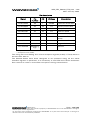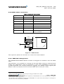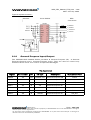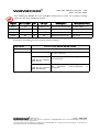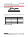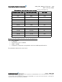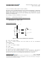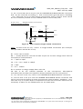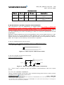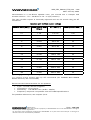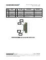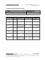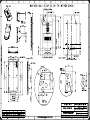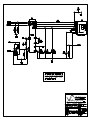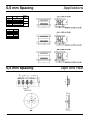
1
WISMO Quik Q2400 series
Q2406 and Q2426
Product Specification
Reference: WM_PRJ_Q2400_PTS_002
Revision: 002
Date: 24th January 2003
Page : 1 / 81
confidential ©
This document is the sole and exclusive property of WAVECOM. Not to be distributed or divulged
without prior written agreement.
Ce document est la propriété exclusive de WAVECOM. Il ne peut être communiqué ou divulgué à
des tiers sans son autorisation préalable.
WM_PRJ_Q2400_PTS_002 - 002
24th January 2003
Document Information
Revision
001
Date
24 Oct 02
History of the evolution
Creation (Preliminary version)
002
24 Jan. 03
Remove “Preliminary” status.
Modification in applicable products list:
•
Add Q2406D and Q2426D products and
Q2406E and Q2426E products
•
Remove Q2406C and Q2426C products
Update sensitivity value for GSM850 and
EGSM900 RF bands.
Update mechanical drawing.
Page : 2 / 81
confidential ©
This document is the sole and exclusive property of WAVECOM. Not to be distributed or divulged
without prior written agreement.
Ce document est la propriété exclusive de WAVECOM. Il ne peut être communiqué ou divulgué à
des tiers sans son autorisation préalable.
WM_PRJ_Q2400_PTS_002 - 002
24th January 2003
Overview
This document defines and specifies the WISMO QUIK Q24x6 Series, available
under two GSM/GPRS Cl10 bi band versions:
•
Q2406A: EGSM/GPRS 900/1800 MHz version with 16 Mb of Flash
memory and 2 Mb of SRAM (16/2)
•
Q2406B: EGSM/GPRS 900/1800 MHz version with 32 Mb of Flash
memory and 4 Mb of SRAM (32/4)
•
Q2406D: EGSM/GPRS 900/1800 MHz version with 64 Mb of Flash
memory and 8 Mb of SRAM (64/8). This configuration will be available
for handset application and vertical application where UART2 is not
used.
•
Q2406E: EGSM/GPRS 900/1800 MHz version with 64 Mb of Flash
memory and 4 Mb of SRAM (64/4). This configuration will be available
for handset application and vertical application where UART2 is not
used.
•
Q2426A: EGSM/GPRS 850/1900 MHz version with 16 Mb of Flash
memory and 2 Mb of SRAM (16/2)
•
Q2426B: EGSM/GPRS 850/1900 MHz version with 32 Mb of Flash
memory and 4 Mb of SRAM (32/4)
•
Q2426D: EGSM/GPRS 850/1900 MHz version with 64 Mb of Flash
memory and 8 Mb of SRAM (64/8). This configuration will be available
for handset application and vertical application where UART2 is not
used.
•
Q2426E: EGSM/GPRS 850/1900 MHz version with 64 Mb of Flash
memory and 4 Mb of SRAM (64/4). This configuration will be available
for handset application and vertical application where UART2 is not
used.
Page : 3 / 81
confidential ©
This document is the sole and exclusive property of WAVECOM. Not to be distributed or divulged
without prior written agreement.
Ce document est la propriété exclusive de WAVECOM. Il ne peut être communiqué ou divulgué à
des tiers sans son autorisation préalable.
WM_PRJ_Q2400_PTS_002 - 002
24th January 2003
Contents
Document Information......................................................................... 2
Overview ............................................................................................. 3
Contents.............................................................................................. 4
Caution................................................................................................ 8
Trademarks ......................................................................................... 8
1
1.1
General description....................................................................... 9
General information .................................................................................9
1.2
Functional description ...........................................................................10
1.2.1
RF functionalities ...........................................................................11
1.2.2
Baseband functionalities................................................................11
1.3
2
2.1
Firmware...............................................................................................11
Interfaces ................................................................................... 12
General Purpose Connector (GPC) .........................................................12
2.2
Power supply ........................................................................................13
2.2.1
Power supply description ..............................................................13
2.2.2
Power consumption ......................................................................14
2.3
Electrical information for digital I/O ........................................................16
2.4
LCD interface.........................................................................................17
2.4.1
SPI bus ..........................................................................................17
2.4.2
Two wires interface .......................................................................17
2.5
SPI Auxiliary bus ...................................................................................17
2.6
Keyboard interface.................................................................................18
2.7
Main serial link (UART1) ........................................................................18
2.7.1
Typical implementation with a RS232 Terminal.............................20
2.7.2
Typical implementation with a microprossessor ............................21
2.8
Auxiliary serial link (Uart2).....................................................................21
2.9
SIM
2.9.1
2.9.2
2.9.3
interface .........................................................................................22
General Description .......................................................................22
SIM socket connection ..................................................................24
SIM 3/5V management ..................................................................24
Page : 4 / 81
confidential ©
This document is the sole and exclusive property of WAVECOM. Not to be distributed or divulged
without prior written agreement.
Ce document est la propriété exclusive de WAVECOM. Il ne peut être communiqué ou divulgué à
des tiers sans son autorisation préalable.
WM_PRJ_Q2400_PTS_002 - 002
24th January 2003
2.10
General Purpose Input/Output ...............................................................25
2.11
Analog to Digital Converter....................................................................27
2.12 Audio interface ......................................................................................27
2.12.1 Microphone inputs ........................................................................27
2.12.1.1 Common microphone inputs characteristics ............................28
2.12.1.2 Main Microphone Inputs (MIC2) ..............................................30
2.12.1.3 Auxiliary Microphone Inputs (MIC1) ........................................31
2.12.1.3.1 Differential connection .......................................................31
2.12.1.3.2 Single-ended connection....................................................32
2.12.2 Common speaker outputs characteristics ......................................33
2.12.2.1 Differential Connection.............................................................33
2.12.2.2 Single-ended Connection .........................................................33
2.12.3 Speaker outputs ............................................................................35
2.12.3.1 Speaker 2 Outputs ...................................................................35
2.12.3.2 Speaker 1 Outputs ...................................................................35
2.12.4 Buzzer Output ...............................................................................35
2.13 Battery charging interface .....................................................................36
2.13.1 Li-ion charging procedure ..............................................................38
2.13.2 How to define R1 and C1...............................................................38
2.14 ON / ~OFF ..........................................................................................39
2.14.1 Operating sequences .....................................................................40
2.14.1.1 Power ON ................................................................................40
2.14.1.2 Power OFF...............................................................................41
2.15
BOOT (optional).....................................................................................41
2.16 Reset signal (~RST) ...............................................................................42
2.16.1 Reset sequence .............................................................................44
2.17
External Interrupt (~INTR) .....................................................................44
2.18
VCC output ..........................................................................................45
2.19 VCC_RTC (Real Time Clock Supply)........................................................45
2.19.1 Interface description ......................................................................45
2.19.2 Typical implementation..................................................................46
2.19.2.1 Capacitor .................................................................................46
2.19.2.2 Super Capacitor .......................................................................46
2.19.2.3 Battery cell with regulator........................................................47
2.19.2.4 Non Rechargeable battery........................................................47
2.20 RF interface ..........................................................................................48
2.20.1 RF connections ..............................................................................48
2.20.2 RF performances ...........................................................................48
2.20.3 Antenna specifications ..................................................................49
Page : 5 / 81
confidential ©
This document is the sole and exclusive property of WAVECOM. Not to be distributed or divulged
without prior written agreement.
Ce document est la propriété exclusive de WAVECOM. Il ne peut être communiqué ou divulgué à
des tiers sans son autorisation préalable.
WM_PRJ_Q2400_PTS_002 - 002
24th January 2003
3
Technical specifications ............................................................. 50
3.1
General Purpose Connector pin out description .....................................50
3.2
Environmental Specifications.................................................................54
3.3
Mechanical specifications......................................................................55
3.3.1
Physical characteristics..................................................................55
3.3.2
Mechanical drawings ....................................................................55
4
Connectors and peripheral devices references............................ 57
4.1
General Purpose Connector ...................................................................57
4.2
SIM Card Reader ...................................................................................57
4.3
Microphone ...........................................................................................57
4.4
Speaker .................................................................................................58
4.5
Antenna Cable.......................................................................................58
4.6
GSM antenna ........................................................................................58
5
Design Guidelines ....................................................................... 59
5.1
HARDWARE and RF ..............................................................................59
5.1.1
EMC recommendations .................................................................59
5.1.2
Power Supply ................................................................................59
5.1.3
Layout requirement .......................................................................60
5.1.4
Antenna.........................................................................................62
5.2
Mechanical integration ..........................................................................62
5.3
Firmware upgrade .................................................................................62
5.3.1
Nominal upgrade procedure ..........................................................62
5.3.2
Backup procedure..........................................................................63
6
Appendix..................................................................................... 64
6.1
Wavecom acceptance test.....................................................................64
6.2
Standards and Recommendations .........................................................66
6.3
Safety recommendations (for information only) .....................................69
6.3.1
RF safety .......................................................................................69
6.3.1.1
General ....................................................................................69
6.3.1.2
Exposure to RF energy.............................................................69
6.3.1.3
Efficient terminal operation ......................................................69
6.3.1.4
Antenna care and replacement ................................................70
6.3.2
General safety................................................................................70
6.3.2.1
Driving.....................................................................................70
6.3.2.2
Electronic devices ....................................................................70
6.3.2.3
Vehicle electronic equipment ...................................................70
6.3.2.4
Medical electronic equipment ..................................................70
6.3.2.5
Aircraft ....................................................................................71
6.3.2.6
Children ...................................................................................71
6.3.2.7
Blasting areas ..........................................................................71
6.3.2.8
Potentially explosive atmospheres ...........................................71
Page : 6 / 81
confidential ©
This document is the sole and exclusive property of WAVECOM. Not to be distributed or divulged
without prior written agreement.
Ce document est la propriété exclusive de WAVECOM. Il ne peut être communiqué ou divulgué à
des tiers sans son autorisation préalable.
WM_PRJ_Q2400_PTS_002 - 002
24th January 2003
Application notes for the SIM interface..................................................72
6.4
6.4.1
Application note #1 : interfacing 3V SIMs......................................73
6.4.2
Application note #2 : interfacing 3V/5V SIMs.................................74
6.5
General Purpose Connector data sheet ..................................................75
Page : 7 / 81
confidential ©
This document is the sole and exclusive property of WAVECOM. Not to be distributed or divulged
without prior written agreement.
Ce document est la propriété exclusive de WAVECOM. Il ne peut être communiqué ou divulgué à
des tiers sans son autorisation préalable.
WM_PRJ_Q2400_PTS_002 - 002
24th January 2003
Caution
Information furnished herein by Wavecom are accurate and reliable. However
no responsibility is assumed for its use. Please read carefully the safety
precautions for a terminal based on WISMO Quik Q24x6 Series.
General information about Wavecom and its range of products is available at
the following internet address: http://www.wavecom.com
Trademarks
Some mentioned products are registered trademarks of their respective
companies.
Page : 8 / 81
confidential ©
This document is the sole and exclusive property of WAVECOM. Not to be distributed or divulged
without prior written agreement.
Ce document est la propriété exclusive de WAVECOM. Il ne peut être communiqué ou divulgué à
des tiers sans son autorisation préalable.
WM_PRJ_Q2400_PTS_002 - 002
24th January 2003
1 General description
1.1 General information
WISMO Quik Q24x6 is a self-contained E-GSM/GPRS 900/1800 or 850/1900 biband module including the following features :
•
•
•
•
•
•
•
•
•
•
•
•
58.4 x 32.2 x 3.9 mm
2 Watts EGSM 900/GSM 850 radio section running under 3.6 Volts
1 Watt GSM1800/1900 radio section running under 3.6 Volts
Digital section running under 2.8 Volts
3V SIM interface
Real Time Clock with calendar
Battery charger
Echo Cancellation + noise reduction
Full GSM or GSM/GPRS software stack
Hardware GPRS class 10 capable
Complete shielding
Complete interfacing :
o Power supply
o Serial link
o Audio
o SIM card
o Keyboard
o LCD (not available with AT commands)
WISMO Quik Q24x6 Series has two external connections :
•
•
RF connection pads (to the antenna)
General Purpose Connector (GPC) to Digital, Keyboard, Audio and Supply
WISMO Quik Q24x6 Series is designed to fit in very small terminals and only
some custom functions have to be added to make a complete bi-band solution:
•
•
•
•
•
•
Keypad and LCD module
Earpiece and Microphone
Base connector
Battery
Antenna switch
SIM connector
Page : 9 / 81
confidential ©
This document is the sole and exclusive property of WAVECOM. Not to be distributed or divulged
without prior written agreement.
Ce document est la propriété exclusive de WAVECOM. Il ne peut être communiqué ou divulgué à
des tiers sans son autorisation préalable.
WM_PRJ_Q2400_PTS_002 - 002
24th January 2003
1.2 Functional description
Power Supply
G
E
N
E
R
A
L
P
U
R
P
O
S
E
C
O
N
N
E
C
T
O
R
RF Interface
RF
I/O Controller
Battery
Management
A/D Converter
SIM Supply
SIM Controller
RF
CPU
FLASH
SRAM
Memory
Management
Unit
C
O
N
N
E
C
T
I
O
N
F
U
N
C
T
I
O
N
S
R.T.C
GPSI Controller
Audio Interface
Vocoder
Keyboard
Controller
UART
Figure 1 : Functional architecture
Page : 10 / 81
confidential ©
This document is the sole and exclusive property of WAVECOM. Not to be distributed or divulged
without prior written agreement.
Ce document est la propriété exclusive de WAVECOM. Il ne peut être communiqué ou divulgué à
des tiers sans son autorisation préalable.
WM_PRJ_Q2400_PTS_002 - 002
24th January 2003
1.2.1 RF functionalities
The Radio Frequency (RF) functionalities comply with the Phase II EGSM
900/GSM 1800 and GSM 850/GSM 1900 recommendation. The frequencies
are :
Q2406
•
Rx (EGSM 900): 925 to 960 MHz Rx (GSM 1800): 1805 to 1880 MHz
•
Tx (EGSM 900): 880 to 915 MHz Tx (GSM 1800): 1710 to 1785 MHz
Q2426
•
Rx (EGSM 850) : 869 to 894 MHz Rx (GSM 1900) : 1930 to 1990 MHz
•
Tx (EGSM 850) : 824 to 849 MHz Tx (GSM 1900) : 1850 to 1910 MHz
The Radio Frequency (RF) part is based on a specific dual band chip including :
•
•
•
•
•
•
Low-if Receiver
Dual RF (Radio Frequency) synthesizer
Digital if to Baseband Converter
Offset PLL (Phase Lock Loop) transmitter
1 (logarithmic) Power Amplifier (PA) controller
Dual band (Power Amplifier (PA) module
1.2.2 Baseband functionalities
The digital part of the WISMO Quik Q24x6 Series is composed of a PHILIPSVLSI chip (ONE C GSM/GPRS Kernel). This chipset is using a 0,25 µm mixed
technology CMOS, which allows massive integration as well as low current
consumption.
1.3 Firmware
WISMO Quik Q24x6 Series is designed to be integrated into various types of
applications
such
as handsets
or
vertical
applications
(telemetry,
multimedia,…).
For
the
not
the
vertical applications, the firmware offers a set of AT commands to control
module. With this standard software, some interfaces of the module are
available since they are dependent on the peripheral devices connected to
module. They are the LCD interface and the SPI bus.
Page : 11 / 81
confidential ©
This document is the sole and exclusive property of WAVECOM. Not to be distributed or divulged
without prior written agreement.
Ce document est la propriété exclusive de WAVECOM. Il ne peut être communiqué ou divulgué à
des tiers sans son autorisation préalable.
WM_PRJ_Q2400_PTS_002 - 002
24th January 2003
2 Interfaces
2.1 General Purpose Connector (GPC)
A 60 pins connector1 is provided to interface the WISMO Quik Q24x6 Series
with a board containing either a LCD module, or a keyboard, or a SIM
connector, or a battery connection...
The interfaces available on the GPC are described in the next paragraphs.
! Please be aware that some of these interfaces can not be handled when
using the WISMO Quik Q24x6 Series driven by AT commands : LCD interface,
SPI bus.
AT
This symbol is used to indicate the interfaces not available with AT
commands.
These functions have then to be managed externally i.e using the main
processor of the application.
1
The communication interface connector is a 60 pins connector with 0.5mm pitch from KYOCERA
/ AVX group with the following reference (see chapter connectors reference for further details):
14 5087 060 930 861.
The matting connector has the following reference :
24 5087 060 X00 861.
Page : 12 / 81
confidential ©
This document is the sole and exclusive property of WAVECOM. Not to be distributed or divulged
without prior written agreement.
Ce document est la propriété exclusive de WAVECOM. Il ne peut être communiqué ou divulgué à
des tiers sans son autorisation préalable.
WM_PRJ_Q2400_PTS_002 - 002
24th January 2003
2.2 Power supply
2.2.1 Power supply description
The power supply is one of the key issue in the design of a GSM terminal. Due
to the bursted emission in GSM / GPRS, the power supply must be able to
deliver high current peaks in a short time. During these peaks the ripple (Uripp)
and the drop (Udrop) on the supply voltage must not exceed a certain limit (see
table “Power Supply Voltage” bellow).
•
In communication mode, a GSM/GPRS classe 2 terminal emits 577µs
radio bursts every 4.615ms.
Udrop
Udrop
Uripp
Uripp
t = 577 µs
T = 4,615 ms
In communication mode, a GPRS class 10 terminal emits 1154µs radio bursts
every 4.615ms.
Two different inputs are provided for the power supply. The first one, VBATT is
used to supply the RF part and VDD, the second one is used to supply the
baseband part.
Notes :
•
It is possible to connect VBATT to VDD.
•
In case of separate power supplies, they have to be in the same state i.e
both active or inactive at the same time.
VBATT : supplies directly the RF components with 3,6 V. It is essential to keep
a minimum voltage ripple at this connection in order to avoid any phase error.
The RF Power Amplifier current (2.0 A peak in GSM /GPRS mode) flows with a
ratio of 1/8 of the time (around 577µs every 4.615ms for GSM /GPRS cl 2) and
2/8 of the time (around 1154µs every 4.615ms for GSM /GPRS cl 10). The
rising time is around 10µs.
Page : 13 / 81
confidential ©
This document is the sole and exclusive property of WAVECOM. Not to be distributed or divulged
without prior written agreement.
Ce document est la propriété exclusive de WAVECOM. Il ne peut être communiqué ou divulgué à
des tiers sans son autorisation préalable.
WM_PRJ_Q2400_PTS_002 - 002
24th January 2003
VDD : supplies the +2.8V ballast regulators of the WISMO QUIK Q24x6. It is
essential to keep the voltage over 3.1 volts.
The WISMO QUIK Q24x6 Series shielding case is the grounding. The ground
has to be connected on the mother board through a complete layer on the PCB.
Power Supply Voltage
VBATT
VMIN
VNOM
VMAX
Ripple max (Uripp)
3.3 V (*)
3.6 V
4.5 V (**)
50 mVpp for freq<200kHz
500 µVpp for freq>200kHz
VDD
3.1 V
4.5 V
100 mVpp
(*) : This value has to be guarantied during the burst (with 2.0A Peak in GSM
or GPRS mode)
(**) : max operating Voltage Stationary Wave Ratio (VSWR) 2:1
When supplying the module with a battery,
(battery+protections+PCB)should be <150 mOhms
the
total
impedance
2.2.2 Power consumption
Following information are given assuming a 50 Ω RF output.
Power consumption in OFF mode
(module supplied, OFF state, no software running)
Overall
consumption
Conditions
INOM
IMAX
Off
5 µA
10 µA
Page : 14 / 81
confidential ©
This document is the sole and exclusive property of WAVECOM. Not to be distributed or divulged
without prior written agreement.
Ce document est la propriété exclusive de WAVECOM. Il ne peut être communiqué ou divulgué à
des tiers sans son autorisation préalable.
WM_PRJ_Q2400_PTS_002 - 002
24th January 2003
Power consumption in EGSM/GPRS 900 MHz and GSM/GPRS 850 MHz mode
classe 10
Conditions
INOM
IMAX
VBATT
During TX bursts @Pcl5
1.7 A peak
2.0 A peak
VBATT
During RX bursts
75 mA peak
80 mA peak
VBATT
Average 1Rx/1Tx @Pcl5
270 mA
320 mA
VBATT
Average 1Rx/1Tx @Pcl8
180 mA
200 mA
VBATT
Average Idle mode
100 µA
300 µA
VBATT
Average GPRS Cl 10
(3Rx/2Tx) @Pcl5
540 mA
640 mA
VBATT
Average GPRS Cl 10
(3Rx/2Tx) @Pcl8
360 mA
400 mA
VDD
Average Idle mode
2,2 mA
3 mA
Power Control Level : Pcl5=2W typ. ; Pcl8=0,5W typ.
Power consumption in GSM/GPRS 1800 MHz and
GSM/GPRS 1900 MHz mode classe 10
Conditions
INOM
IMAX
VBATT
During TX bursts @Pcl0
1.3 A peak
1.7 A peak
VBATT
During RX bursts
75 mA peak
80 mA peak
VBATT
Average 1Rx/1Tx @Pcl0
240 mA
270 mA
VBATT
Average 1Rx/1Tx @Pcl3
150 mA
180 mA
VBATT
Average Idle mode
100 µA
300 µA
VBATT
Average GPRS Cl 10
(3Rx/2Tx) @Pcl0
480 mA
540 mA
VBATT
Average GPRS Cl 10
(3Rx/2Tx) @Pcl3
300 mA
360 mA
VDD
Average Idle mode
2,2 mA
3 mA
Power Control Level : Pcl0=1W typ. ; Pcl3=0,25W typ.
Page : 15 / 81
confidential ©
This document is the sole and exclusive property of WAVECOM. Not to be distributed or divulged
without prior written agreement.
Ce document est la propriété exclusive de WAVECOM. Il ne peut être communiqué ou divulgué à
des tiers sans son autorisation préalable.
WM_PRJ_Q2400_PTS_002 - 002
24th January 2003
Power Supply Pinout
Signal
Pin number
VBATT
55, 57, 58, 59 60
VDD
11
GND
Shielding
The grounding connection is done through the shielding " the four legs have
to be soldered to the ground plane.
2.3 Electrical information for digital I/O
All digital I/O comply with 3Volts CMOS.
Operating conditions
Parameter
I/O type
Min
Max
VIL
CMOS
-0.5 V
0.8 V
VIH
CMOS
2.1 V
3.0 V
VOL
1X
0.2 V
IOL = -1 mA
2X
0.2 V
IOL = -2 mA
3X
0.2 V
IOL = -3 mA
VOH
Condition
1X
2.6 V
IOH = 1 mA
2X
2.6 V
IOH = 2 mA
3X
2.6 V
IOH = 3 mA
To interface the WISMO Quik Q24x6 Series digital signals with other logics :
•
3V logic : some serial resistors (between 2.2K and 4.7Kohms) can be
added on the lines
•
3.3V logic : some serial resistors (between 4.7K and 10Kohms) can be
added on the lines.
•
For higher voltage logics, a resistor bridge or a level shifter IC can be
added.
Page : 16 / 81
confidential ©
This document is the sole and exclusive property of WAVECOM. Not to be distributed or divulged
without prior written agreement.
Ce document est la propriété exclusive de WAVECOM. Il ne peut être communiqué ou divulgué à
des tiers sans son autorisation préalable.
WM_PRJ_Q2400_PTS_002 - 002
24th January 2003
2.4 LCD interface
A
AT
T
The WISMO Quik Q24x6 Series can be connected to a LCD module driver
through either a SPI bus or a two wires interface.
2.4.1 SPI bus
The SPI bus includes a CLK signal, an IO signal and an EN signal complying
with SPI bus standard.
Pin description
Signal
Pin number
I/O
I/O type
SPI_CLK
10
O
1X
SPI_IO
8
I/O
CMOS / 1X
SPI_EN *
28
O
1X
Description
SPI Serial Clock
SPI Data
SPI Enable
* Multiplexed with GPO3.
2.4.2 Two wires interface
The two wires interface includes a CLK signal and a DATA signal complying
with a standard 96KHz interface. The maximum speed transfer is 400Kb/s.
Pin description
Signal
A
AT
T
Pin number
I/O
I/O type
Description
Serial Clock
SCL
10
O
1X
SDA
8
I/O
CMOS / 1X
Data
2.5 SPI Auxiliary bus
A second SPI Chip Enable (called SPI_AUX) has to be used to add a SPI
peripheral to the WISMO Quik Q24x6 Series.
Pin description
Signal
Pin number
I/O
I/O type
SPI_CLK
10
O
1X
SPI_IO
8
I/O
CMOS / 1X
SPI_AUX *
26
O
1X
Description
SPI Serial Clock
SPI Data
SPI Aux. Enable
* Multiplexed with GPO0.
Page : 17 / 81
confidential ©
This document is the sole and exclusive property of WAVECOM. Not to be distributed or divulged
without prior written agreement.
Ce document est la propriété exclusive de WAVECOM. Il ne peut être communiqué ou divulgué à
des tiers sans son autorisation préalable.
WM_PRJ_Q2400_PTS_002 - 002
24th January 2003
2.6 Keyboard interface
! Warning :
This interface is not FULLY available with AT commands :
An AT command allows to get the input key code (see +CMER command
description). This code has then to be processed by the application.
This interface provides 10 connections : 5 rows (R0 to R4) and 5 columns (C0
to C4).
The scanning is a digital one , and the debouncing is done in the WISMO Quik
Q24x6 Series. No discrete components like R,C (Resistor, Capacitor) are
needed.
Pin description
Signal
Pin number
I/O
I/O type
Description
ROW0
13
I/O
CMOS / 1X
Row scan
ROW1
15
I/O
CMOS / 1X
Row scan
ROW2
17
I/O
CMOS / 1X
Row scan
ROW3
19
I/O
CMOS / 1X
Row scan
ROW4
21
I/O
CMOS / 1X
Row scan
COL0
23
I/O
CMOS / 1X
Column scan
COL1
25
I/O
CMOS / 1X
Column scan
COL2
27
I/O
CMOS / 1X
Column scan
COL3
29
I/O
CMOS / 1X
Column scan
COL4
31
I/O
CMOS / 1X
Column scan
2.7 Main serial link (UART1)
A flexible 6 wires serial interface is available complying with V24 protocol
signalling but not with V28 (electrical interface) due to a 2.8 Volts interface.
The signals are TX data (CT103/TX), RX data (CT104/RX), Request To Send
(CT105/RTS), Clear To Send (CT106/CTS), Data Terminal Ready (CT108-2/DTR)
and Data Set Ready (CT107/DSR).
The set of RS232 signals can be required for GSM DATA services application
and is generated by the general purpose I/O provided by the Q24x6 series.
The 2 additional signals are Data Carrier Detect (CT109/DCD) and Ring
Indicator (CT125/RI).
Page : 18 / 81
confidential ©
This document is the sole and exclusive property of WAVECOM. Not to be distributed or divulged
without prior written agreement.
Ce document est la propriété exclusive de WAVECOM. Il ne peut être communiqué ou divulgué à
des tiers sans son autorisation préalable.
WM_PRJ_Q2400_PTS_002 - 002
24th January 2003
Pin description
Signal
Pin
number
I/O
I/O type
Description
CT103/TXD1
39
I
CMOS
Transmit serial data
CT104/RXD1
32
O
1X
CT105/RTS1
30
I
CMOS
CT106/CTS1
37
O
1X
Clear To Send
CT107/DSR1
36
O
1X
Data Set Ready
CT108-2/DTR1
34
I
CMOS
CT109/DCD1 *
51
O
CMOS / 2X Data Carrier Detect
CT125/RI1 **
54
O
CMOS / 2X Ring Indicator
CT102/GND
Shielding
legs
Receive serial data
Ready To Send
Data
Ready
Terminal
Ground
* Multplexed with GPIO3
** Multplexed with GPIO2.
The rising time and falling time of the reception signals (mainly CT103) have to
be less than 200 ns.
The Q24x6 Series have been designed to be operated using all the serial
interface signals. In particular, it is necessary to use RTS and CTS for hardware
flow control in order to avoid data corruption during transmission.
Page : 19 / 81
confidential ©
This document is the sole and exclusive property of WAVECOM. Not to be distributed or divulged
without prior written agreement.
Ce document est la propriété exclusive de WAVECOM. Il ne peut être communiqué ou divulgué à
des tiers sans son autorisation préalable.
WM_PRJ_Q2400_PTS_002 - 002
24th January 2003
2.7.1 Typical implementation with a RS232 Terminal
The figure above shows a typical implementation when the Q24x6 Module is
connected to a RS232 Terminal.
+3V
+3V
VCC
+3V
WARNING:
The application must allow the WISMO serial link signals + the BOOT, the
RESET and the ON/OFF module signals to be easily accessed thus allowing the
module firmware to be upgraded.
Page : 20 / 81
confidential ©
This document is the sole and exclusive property of WAVECOM. Not to be distributed or divulged
without prior written agreement.
Ce document est la propriété exclusive de WAVECOM. Il ne peut être communiqué ou divulgué à
des tiers sans son autorisation préalable.
WM_PRJ_Q2400_PTS_002 - 002
24th January 2003
2.7.2 Typical implementation with a microprossessor
The figure above shows a typical implementation when the Q24x6 Module is
connected to a host microprocessor which is 2,8 V tolerant on the serial port
signals.
Host Microprocessor
A
AT
T
2.8 Auxiliary serial link (Uart2)
For future applications (e.g. Bluetooth connectivity) au auxiliary serial interface
(UART2) will be available on Q24x6A and Q24x6B products.
! Warning :
The auxiliary serial link (UART2) is not available on Q24x6D and Q24x6E
products (version with 64 Mb of Flash memory and 8 Mb of SRAM).
Pin description
Pin
I/O
I/O
type
Description
Multiplexed
with
CT104 / TXD2
18
I
3X
Receive serial data
GPI
CT103 / RXD2
20
O
CMOS
Transmit serial data
GPO2
CT106 / CTS2
24
I
CMOS
Clear To Send
GPIO0
CT105 / RTS2
35
O
2X
Ready To Send
GPIO5
Signal
number
Page : 21 / 81
confidential ©
This document is the sole and exclusive property of WAVECOM. Not to be distributed or divulged
without prior written agreement.
Ce document est la propriété exclusive de WAVECOM. Il ne peut être communiqué ou divulgué à
des tiers sans son autorisation préalable.
WM_PRJ_Q2400_PTS_002 - 002
24th January 2003
2.9 SIM interface
2.9.1 General Description
5 signals exist :
•
•
•
•
•
SIMVCC : SIM power supply.
SIMRST : reset.
SIMCLK : clock.
SIMDATA : I/O port.
SIMPRES : SIM card detect.
The SIM interface controls a 3V SIM (and a 5V SIM through an external SIM
driver). This interface is fully compliant with GSM 11.11 recommendations
concerning SIM functions.
It is recommended to add Transient Voltage Suppressor diodes on the signal
connected to the SIM socket in order to prevent any ElectroStatic Discharge.
TVS diodes with low capacitance (less than 10pF) have to be connected on
SIMCLK and SIMDATA to avoid any disturbance of the rising and falling edge.
These types of diodes are mandatory for the Full Type Approval. They shall be
placed as close as possible to the SIM socket.
The following references can be used : DALC208SC6 from ST Microelectronics.
Pin description
Signal
Pin number
I/O
I/O type
Description
SIMCLK
3
O
2X
SIM Clock
SIMRST
5
O
2X
SIM Reset
SIMDATA
7
I/O
CMOS / 3X
SIM Data
SIMVCC
9
O
SIMPRES
50
I
SIM Power Supply
CMOS
SIM Card Detect
Page : 22 / 81
confidential ©
This document is the sole and exclusive property of WAVECOM. Not to be distributed or divulged
without prior written agreement.
Ce document est la propriété exclusive de WAVECOM. Il ne peut être communiqué ou divulgué à
des tiers sans son autorisation préalable.
WM_PRJ_Q2400_PTS_002 - 002
24th January 2003
Electrical Characteristics
Parameter
Conditions
SIMDATA VIH
IIH = ± 20µA
SIMDATA VIL
IIL = 1mA
SIMRST,
Source
20µA
SIMDATA
Min
Typ
Max
0.7xSIMVCC
Unit
V
0.3xSIMVC
V
C
current
=
V
SIMVCC – 0.1V
SIMCLK VOH
SIMRST,
SIMDATA
Sink current
200µA
=
-
0.1
V
2.85
V
SIMCLK VOL
SIMVCC*
Output
Voltage
ISIMVCC <= 6mA
2.70
2.80
SIMCLK
Rise/Fall Time
Loaded with 30pF
50
ns
SIMRST,
SIMDATA
Rise/Fall Time
Loaded with 30pF
1
µs
SIMCLK
Frequency
Loaded with 30pF
3.25
MHz
(*) : given for the 3V interface. An external SIM driver is needed to handle 5V
SIMs.
Note :
When not used SIMPRES has to be tied to VCC.
When used, a low to high transition means that the SIM card is inserted and a
high to low transition means that the SIM card is removed.
Page : 23 / 81
confidential ©
This document is the sole and exclusive property of WAVECOM. Not to be distributed or divulged
without prior written agreement.
Ce document est la propriété exclusive de WAVECOM. Il ne peut être communiqué ou divulgué à
des tiers sans son autorisation préalable.
WM_PRJ_Q2400_PTS_002 - 002
24th January 2003
2.9.2 SIM socket connection
SIM socket pin description
Signal
Pin number
Description
VCC
1
SIMVCC
RST
2
SIMRST
CLK
3
SIMCLK
CC4
4
VCC module
GND
5
GROUND
VPP
6
Not connected
I/O
7
SIMDATA
CC8
8
SIMPRES with 100kΩ pull
down resistor
SIMVCC
1 VCC
SIMRST
2 RST
SIMCLK
3
VCC
CLK
4 CC4
5 GND
C
GND
VPP
SIMDATA
7
SIMPRES
8 CC8
I/O
100
kW
470pf
GND
Figure 2 : SIM socket
The capacitor placed on the Sim Vcc must not exceed 470nF.
2.9.3 SIM 3/5V management
The WISMO Quik Q24x6 Series module is designed to interface with 3V SIMs
only2.
Nevertheless, it is possible to manage 3V and 5V SIMs using an external level
shifter (see application notes in appendix). In this case, depending on the type
of SIM detected, the module firmware triggers the GPO0 output signal (pin
#26) in order to properly set the external SIM driver level (3V or 5V).
2
Most of the GSM operators have been providing 3V SIMs since 1998.
Page : 24 / 81
confidential ©
This document is the sole and exclusive property of WAVECOM. Not to be distributed or divulged
without prior written agreement.
Ce document est la propriété exclusive de WAVECOM. Il ne peut être communiqué ou divulgué à
des tiers sans son autorisation préalable.
WM_PRJ_Q2400_PTS_002 - 002
24th January 2003
Typical implementation :
Module
Level Shifter
SIM
Connector
VCC
100Ω
C_SIMCLK
C_SIMRST
C_SIMDATA
C_SIMVCC
2.10
General Purpose Input/Output
The WISMO Quik Q24x6 Series provides 6 General Purpose I/O, 4 General
Purpose Outputs and 1 General Purpose Input. They are used to control any
external device such as a LCD or a Keyboard backlight.
Pin description
Signal
Pin number
I/O
I/O type
Description
Multiplexed with
GPIO0
24
I/O
CMOS / 2X
General Purpose I/O
GPIO4
53
I/O
CMOS / 2X
General Purpose I/O
GPIO5
35
I/O
CMOS / 2X
General Purpose I/O
GPO1
22
O
3X
General Purpose O
GPO2
20
O
1X
General Purpose O
TXD2
GPI
18
I
CMOS
General Purpose I
RXD2
GPO3
28
O
CMOS
General Purpose O
SPI_EN
RTS2
CTS2
Page : 25 / 81
confidential ©
This document is the sole and exclusive property of WAVECOM. Not to be distributed or divulged
without prior written agreement.
Ce document est la propriété exclusive de WAVECOM. Il ne peut être communiqué ou divulgué à
des tiers sans son autorisation préalable.
WM_PRJ_Q2400_PTS_002 - 002
24th January 2003
A
AT
T
The following GPIOs are not available (reserved) in case of module running
with the AT commands firmware :
Signal
Pin number
I/O
I/O type
Description
Multiplexed with
GPIO1
52
I/O
CMOS / 2X
General Purpose I/O
FLASH LED(*)
GPIO2
54
I/O
CMOS / 2X
General Purpose I/O
CT125/RI1
GPIO3
51
I/O
CMOS / 2X
General Purpose I/O
CT109/DCD1
GPO0
26
O
3X
General Purpose O
SPI_AUX
(*) The FLASH LED signal can be used to drive a LED through an open-collector
transistor according to the module activity status.
LED status
WISMO Quik Q24x6 Series status
OFF
Module in download mode or module OFF
ON
Permanent
Module switched ON, not registered
on the network
Slow flash
Module switched ON, registered on
the network
LED ON for 200ms,
OFF for 2s
Module switched ON, registered on
the
network,
communication
in
LED ON for 200ms,
progress
OFF for 600ms
Quick flash
Page : 26 / 81
confidential ©
This document is the sole and exclusive property of WAVECOM. Not to be distributed or divulged
without prior written agreement.
Ce document est la propriété exclusive de WAVECOM. Il ne peut être communiqué ou divulgué à
des tiers sans son autorisation préalable.
WM_PRJ_Q2400_PTS_002 - 002
24th January 2003
2.11
Analog to Digital Converter
Analog to Digital converter input is provided by the WISMO Quik Q24x6 Series.
This converter is a 10 bits one, ranging from 0 to 2.8V .
Pin description
Signal
Pin number
I/O
I/O type
Description
AUXV0
33
I
Analog
A/D converter
Electrical Characteristics
Parameter
Min
Resolution
Sampling rate
Input signal range
Unit
10
bits
90.3
Ksps
0
2.8V
V
ADC Reference Accuracy
0.75
2
%
Integral Accuracy
+/- 1
LSB
Differential Accuracy
+/- 1
LSB
Input Impedance ( R )
10
MΩ
Input Impedance ( C )
2.12
Max
100
nF
Audio interface
Two different microphone inputs and two different speaker outputs are
supported.
The WISMO Quik Q24x6 Series also includes an echo cancellation feature
which allows handsfree function.
2.12.1 Microphone inputs
The MIC2 inputs already include the biasing for an electret microphone
allowing an easy connection to a handset.
The MIC1 inputs do not include an internal bias. MIC1/SPK1 is then
appropriate for a hands free system or a handset with biasing external to the
module.
Page : 27 / 81
confidential ©
This document is the sole and exclusive property of WAVECOM. Not to be distributed or divulged
without prior written agreement.
Ce document est la propriété exclusive de WAVECOM. Il ne peut être communiqué ou divulgué à
des tiers sans son autorisation préalable.
WM_PRJ_Q2400_PTS_002 - 002
24th January 2003
2.12.1.1 Common microphone inputs characteristics
The connection can be either differential or single-ended but using a differential
connection in order to reject common mode noise and TDMA noise is strongly
recommended. When using a single-ended connection, be sure to have a very
good ground plane, a very good filtering as well as shielding in order to avoid
any disturbance on the audio path.
Internal audio filter characteristics
Frequency
Gain
0-150 Hz
< -22dB
150-180 Hz
< -11dB
180-200 Hz
< -3dB
200-3700 Hz
0dB
>4000 Hz
< -60dB
The gain of MIC inputs is internally adjusted and can be tuned from 30dB to
51dB using an AT command.
Microphone gain vs Max input voltage (using controller 1)
Transmit Gain (dB)
Max Vin (mVrms)
AT+VGT(*)
30
43.80
0 to 31
33
31.01
32 to 63
36
21.95
64 to 95
39
15.54
96 to 127
42
11
128 to 159
45
7.79
160 to 191
48
5.51
192 to 223
51
3.9
224 to 255
(*) control of the transmit gain by AT commands (for WISMO Quik Q24x6
Series driven by AT commands)
Page : 28 / 81
confidential ©
This document is the sole and exclusive property of WAVECOM. Not to be distributed or divulged
without prior written agreement.
Ce document est la propriété exclusive de WAVECOM. Il ne peut être communiqué ou divulgué à
des tiers sans son autorisation préalable.
WM_PRJ_Q2400_PTS_002 - 002
24th January 2003
Microphone gain vs Max input voltage (using controller 2)
Transmit Gain (dB)
Max Vin (mVrms)
AT+VGT
- 6.5
3031
128 to 243
-6.0
2861
224
…
…
…
0.0
1434
0
…
…
…
+9.5
480
19
+10.0
454
20
+ 30.3
43.80
21 to 60
+ 30.8
41.36
61
…
…
…
+ 50.8
4.14
101
+ 51.3
3.90
102 to 127
Recommended characteristics for the microphone:
•
•
•
•
•
2V – 0.5mA
2 KOhms
Sensitivity -40 to –50dB
SNR > 50dB
Frequency response compatible with the GSM specifications
For possible references, see § 4.3.
Page : 29 / 81
confidential ©
This document is the sole and exclusive property of WAVECOM. Not to be distributed or divulged
without prior written agreement.
Ce document est la propriété exclusive de WAVECOM. Il ne peut être communiqué ou divulgué à
des tiers sans son autorisation préalable.
WM_PRJ_Q2400_PTS_002 - 002
24th January 2003
2.12.1.2 Main Microphone Inputs (MIC2)
The MIC2 inputs are differential ones. They already include the convenient
biasing for an electret microphone (0,5 mA and 2 Volts). This electret
microphone can be directly connected on these inputs. The impedance of the
microphone 2 has to be around 2kΩ. These inputs are standard ones for an
handset design while MIC1 inputs can be connected to an external headset or
a handsfree kit.
AC coupling is already embedded in the module.
Typical implementation:
C3
L1
MIC2P
C1
C2
L2
MIC2N
C4
Figure 3 : MIC2 inputs (differential connection)
C1 = 10pF to 33pF
C2 = C3 = C4 = 47pF to 100pF
L1 = L2 = 100nH
C1 has to be the nearest possible to the microphone. Microphone
manufacturers provide this capacitor directly soldered on the microphone.
C2 has to be very close to the WISMO Quik Q24x6 Series connector.
L1, L2, C3 and C4 has to be put near the WISMO Quik Q24x6 Series connector
and can be removed according to their environment (ground plane, shielding,
etc…). The best way is to plan all the components and to remove those which
are not necessary to filter out the TDMA noise on the audio path.
Pin description
Signal
Pin #
I/O
I/O type
Description
MIC2P
46
I
Analog
Microphone 2 positive
input
MIC2N
48
I
Analog
Microphone 2 negative
input
Page : 30 / 81
confidential ©
This document is the sole and exclusive property of WAVECOM. Not to be distributed or divulged
without prior written agreement.
Ce document est la propriété exclusive de WAVECOM. Il ne peut être communiqué ou divulgué à
des tiers sans son autorisation préalable.
WM_PRJ_Q2400_PTS_002 - 002
24th January 2003
2.12.1.3 Auxiliary Microphone Inputs (MIC1)
The MIC1 inputs are differential and do not include internal bias. To use these
inputs with an electret microphone, bias has to be generated outside the
WISMO Quik Q24x6 Series module according to the characteristic of this
electret microphone. These inputs are the standard ones used for an external
headset or a handsfree kit.
AC coupling is already embedded in the module.
2.12.1.3.1
Differential connection
Impedance of the microphone input in differential mode :
•
Module ON : Rin = 10KΩ +/-10%
•
Module OFF : Rin >1MΩ +/-10%
Typical implementation:
VCC
R1
C3
R2
L1
MIC1P
C1
C5
C2
L2
MIC1N
R3
C4
R4
Figure 4 : MIC1 inputs (differential connection)
R1 = R4 = from 100 to 330Ω
R2 = R3 = usually between 1KΩ and 3.3KΩ as per the microphone
characteristics
C1 = 10pF to 33pF
C2 = C3 = C4 = 47pF to 100pF
C5 = 47µF
L1 = L2 = 100nH
R1 and R4 are used as a voltage supply filter with C5.
C1 has to be the nearest possible to the microphone. Microphone
manufacturers provide this capacitor directly soldered on the microphone.
C2 has to be very close to the WISMO Quik Q24x6 Series connector.
Page : 31 / 81
confidential ©
This document is the sole and exclusive property of WAVECOM. Not to be distributed or divulged
without prior written agreement.
Ce document est la propriété exclusive de WAVECOM. Il ne peut être communiqué ou divulgué à
des tiers sans son autorisation préalable.
WM_PRJ_Q2400_PTS_002 - 002
24th January 2003
L1, L2, C3 and C4 has to be put near the WISMO Quik Q24x6 Series connector
and can be removed according to their environment (ground plane, shielding
...etc). The best way is to plan all the components and to remove those which
are not necessary to filter out the TDMA noise on the audio path.
2.12.1.3.2
Single-ended connection
Typical implementation:
VAUDIO
C3
R1
C4
L2
MIC1P
C1
R2
L1
MIC1N
C5
C2
Figure 5 : MIC1 inputs (single-ended connection)
Note : VAUDIO must be very “clean” in single-ended connection (for example,
VCC plus filter cell like RC or LC).
R1 = from 100 to 330Ω
R2 = usually between 1KΩ and 3.3KΩ as per the VAUDIO voltage level and the
microphone characteristics
C1 = 10pF to 33pF
C2 = C3 = C5 = 47pF to 100pF
C4 = 47µF
L1 = L2 = 100nH
R1 is used as a voltage supply filter with C4.
C5 has to be the nearest possible to the microphone. Microphone
manufacturers provide this capacitor directly soldered on the microphone.
C1, C2, C3 have to be very close to the WISMO Quik Q24x6 Series connector.
L1, and L2 has to be put near the WISMO Quik Q24x6 Series connector and
can be removed according to their environment (ground plane, shielding ...etc).
The best way is to plan all the components and to remove those which are not
necessary to filter out the TDMA noise on the audio path.
Page : 32 / 81
confidential ©
This document is the sole and exclusive property of WAVECOM. Not to be distributed or divulged
without prior written agreement.
Ce document est la propriété exclusive de WAVECOM. Il ne peut être communiqué ou divulgué à
des tiers sans son autorisation préalable.
WM_PRJ_Q2400_PTS_002 - 002
24th January 2003
Pin description
Signal
Pin #
I/O
I/O type
Description
MIC1P
42
I
Analog
Microphone 1 positive
input
MIC1N
44
I
Analog
Microphone 1 negative
input
2.12.2 Common speaker outputs characteristics
The connection can be differential or single-ended but using a differential
connection to reject common mode noise and TDMA noise is strongly
recommended. Morover in single-ended mode, ½ of the power is lost. When
using a single-ended connection, be sure to have a very good ground plane, a
very good filtering as well as shielding in order to avoid any disturbance on the
audio path.
Speaker outputs SPK2 are push-pull amplifiers and can be loaded down to 150
Ohms and up to 1nF (see details in table Speaker gain vs Max output voltage).
These outputs are differential and the output power can be adjusted by step of
2dB. The output can be directly connected to a speaker.
2.12.2.1 Differential Connection
Impedance of the speaker amplifier output in differential mode :
•
R ≤ 1Ω +/-10%
SPKxP
SPKxN
Figure 6 : SPK outputs (differential mode)
2.12.2.2 Single-ended Connection
Typical implementation:
C1
C3
Speaker
ZHP
33 to
100pF
SPKxP
+
C2
R1
+
SPKxN
Figure 7 : SPK outputs (single-ended connection)
C1 = from 4.7µF to 47µF as per the speaker characteristics and the output
power.
C1=C2 ; R1= Speaker Impedance
Using a single-ended connection also includes losing half of the output power
compared to a differential connection.
Page : 33 / 81
confidential ©
This document is the sole and exclusive property of WAVECOM. Not to be distributed or divulged
without prior written agreement.
Ce document est la propriété exclusive de WAVECOM. Il ne peut être communiqué ou divulgué à
des tiers sans son autorisation préalable.
WM_PRJ_Q2400_PTS_002 - 002
24th January 2003
Nevertheless in a 32 Ohms speaker case, you should use a cheaper and
smaller solution : R1 = 82 Ohm et C2 = 4.7µF (ceramic)
The gain of SPK outputs is internally adjusted and can be tuned using an AT
command.
Speaker gain vs Max output voltage
Receive Gain (dB) (*)
Max output level
(Vrms)
AT+VGR (**)
Max.speaker load (Ω)
+2
1.74
0 to 15
150
0
1.38
16 to 31
50
-2
1.099
32 to 47
32
-4
0.873
48 to 63
32
-6
0.693
64 to 79
32
-8
0.551
80 to 95
32
-10
0.437
96 to 111
32
-12
0.347
112 to 127
32
-14
0.276
128 to 143
32
-16
0.219
144 to 159
32
-18
0.174
160 to 175
32
-20
0.138
176 to 191
32
-22
0.110
192 to 207
32
-24
0.087
208 to 223
32
-26
0.069
224 to 239
32
-26
0.069
240 to 255
32
(*) analog gain : might not be significant
(**) control of the receive gain by AT commands (for WISMO Quik Q24x6
Series driven by AT commands)
Recommended characteristics for the speaker:
•
•
•
•
Type : 10 mW, electro-magnetic
Impedance : 32 to 150 Ω
Sensitivity : 110 dB SPL min. (0dB = 20µPa)
Frequency response compatible with the GSM specifications
For possible references, see chapter § 4.4.
Page : 34 / 81
confidential ©
This document is the sole and exclusive property of WAVECOM. Not to be distributed or divulged
without prior written agreement.
Ce document est la propriété exclusive de WAVECOM. Il ne peut être communiqué ou divulgué à
des tiers sans son autorisation préalable.
WM_PRJ_Q2400_PTS_002 - 002
24th January 2003
2.12.3 Speaker outputs
2.12.3.1 Speaker 2 Outputs
Pin description
Signal
Pin #
I/O
I/O type
Description
SPK2P
45
O
Analog
Speaker 2 positive output
SPK2N
47
O
Analog
Speaker 2 negative output
2.12.3.2 Speaker 1 Outputs
Pin description
Signal
Pin #
I/O
I/O type
Description
SPK1P
41
O
Analog
Speaker 1 positive output
SPK1N
43
O
Analog
Speaker 1 negative output
2.12.4 Buzzer Output
The buzzer output is a digital one. A buzzer can be directly connected between
this output and VBATT. The maximum current is 80 mA (PEAK). A diode
against transient peak voltage must be connected as described below.
VBATT
D1
C1
???
Figure 8 : Buzzer connection
R1 must be chosen in order to limit the current at IPEAK max.
C1 = 0 to 100 nF (depending on the buzzer type).
Recommended characteristics for the buzzer :
•
•
•
Type : electro-magnetic.
Impedance : 7 to 30 Ω
Sensitivity : 90 dB SPL min @ 10 cm
Pin description
Signal
Pin #
I/O
I/O type
Description
BUZ
49
O
Analog
Buzzer output
Page : 35 / 81
confidential ©
This document is the sole and exclusive property of WAVECOM. Not to be distributed or divulged
without prior written agreement.
Ce document est la propriété exclusive de WAVECOM. Il ne peut être communiqué ou divulgué à
des tiers sans son autorisation préalable.
WM_PRJ_Q2400_PTS_002 - 002
24th January 2003
Operating conditions
2.13
Parameter
Condition
VOL
Min
Max
Unit
Imoy = 40mA
0.6
V
IPEAK
VBATT = VBATTmax
80
mA
IAVERAGE
VBATT = VBATTmax
40
mA
Battery charging interface
The WISMO Quik Q24x6 Series module supports one battery charging circuit
for Li-Ion batteries. This circuit uses an interface which consists of a current
source inputs (CHG_IN) where the constant current has to flow in order to
charge the battery. This current value depends on the battery capacity. It is
recommended to provide a current equal to the value of the capacity plus
50mA. For a 550mA battery the current will be 600mA. The maximum current
is 800mA.
A specific AT command (AT+WBCM), available from 4.3 level, allows to
manage the charge battery (start and stop the charge, enable or disable
unsolicited Battery Charge Indications and set the battery charge parameters).
The WISMO Quik Q24x6 Series module monitors the battery voltage to detect
the end of the charge. WISMO Quik Q24x6 Series also monitors the
temperature of the battery through the BAT_TEMP pin which has to be
connected to a temperature sensor inside the battery (a NTC resistor for
instance).
Pin description
Signal
Pin number
I/O
I/O type
Description
CHG_IN
1, 2, 4
I
Analog
Current source
input
BAT_TEMP
38
I
Analog
A/D converter
Page : 36 / 81
confidential ©
This document is the sole and exclusive property of WAVECOM. Not to be distributed or divulged
without prior written agreement.
Ce document est la propriété exclusive de WAVECOM. Il ne peut être communiqué ou divulgué à
des tiers sans son autorisation préalable.
WM_PRJ_Q2400_PTS_002 - 002
24th January 2003
Electrical Characteristics
Parameter
Min
BAT_TEMP resolution
Max
Typ
10
BAT_TEMP sampling rate
bits
90.3
BAT_TEMP Input Impedance ( R )
Ksps/s
4.7
kΩ
BAT_TEMP Input Impedance ( C )
CHG_IN Voltage (for I=Imax)
Unit
5,1*
CHG_IN Current
100
nF
5,5
V
800
mA
BAT_TEMP Input signal range
2.8
V
* To be parametrized as per battery manufacturer
Internal Battery
Resistor
+VBATT
Safety
Circuitry
VCC
R1
BAT_TEMP
C1
CTN
GND
Figure 9 : Connection examples
Page : 37 / 81
confidential ©
This document is the sole and exclusive property of WAVECOM. Not to be distributed or divulged
without prior written agreement.
Ce document est la propriété exclusive de WAVECOM. Il ne peut être communiqué ou divulgué à
des tiers sans son autorisation préalable.
WM_PRJ_Q2400_PTS_002 - 002
24th January 2003
2.13.1 Li-ion charging procedure
A constant current source has to be provided through CHG_IN input in order to
charge the Li-ion battery, and BAT_TEMP input has to be connected to a
battery temperature sensor. During this procedure the voltage of the battery is
accurately monitored.
The Li-ion charging involves two phases. During the first phase, the battery is
charged with a constant current until its voltage reaches 4.1V*. During the
second phase the constant current is pulsed by the module. The width and the
frequency of the pulse change during this phase in order to ensure a safety
charge. The battery is considered as fully charged when, after a pulse, the
voltage remains at a 4.1V* during more than 10s.
The Li-ion battery must have an included safety circuit to avoid any discharge
or overcharge. This circuit is delivered by the manufacturer inside the battery
pack. The impedance of this safety circuit has to be the lowest possible in
order to reduce the drop-out of the voltage. This drop-out is due to the RF
Power Amplifier current (up to 2.0A). A maximum of 150mΩ is required.
(*) : To be parametrized as per battery manufacturer
2.13.2 How to define R1 and C1
How to choose R1
R1 has to be chosen to have a full range of BAT-TEMP (from 0V to 2.8V) when
the CTN value changes from the minimum to the maximum temperature
How to choose C1
C1 has to be chosen to have a RC filter with a time constant lower than 2ms.
Calculation examples
CTN(25°C) = 47K
CTN(55°C) = 10K
CTN(-10°C) = 300K
CTN(-10°C) x VCC = ( CTN(-10°C) + R1 ) x BAT-TEMP (full range)
R1= 47K " BAT-TEMP(-20°C) = 2.42V
BAT-TEMP(55°C) = 0.49V
R(-20°C) = R1//CTN(-10°C) = 40K
R(+55°C) = 8K
With C= 10nF ::
RC(-20°C) = 400µs
RC(+55°C) = 80µs
Page : 38 / 81
confidential ©
This document is the sole and exclusive property of WAVECOM. Not to be distributed or divulged
without prior written agreement.
Ce document est la propriété exclusive de WAVECOM. Il ne peut être communiqué ou divulgué à
des tiers sans son autorisation préalable.
WM_PRJ_Q2400_PTS_002 - 002
24th January 2003
2.14
ON / ~OFF
This input is used to switch ON or OFF the WISMO Quik Q24x6 Series module.
A high level signal has to be provided on the pin ON/~OFF to switch ON the
module. The level of the voltage of this signal has to be maintained between
2.4V and VDD during a minimum of 1000ms. This signal can be left at high
level until switch off.
To be able to switch OFF the module, the pin ON/OFF has to be released.
Through the firmware, the module can be switched off (using the CPOF
command).
Pin description
Signal
Pin number
I/O
I/O type
Description
ON/∼OFF
6
I
CMOS
Module Power ON
Electrical Characteristics
Parameter
Min
Input Impedance ( R )
10
Max
Unit
kΩ
Input Impedance ( C )
50
pF
Operating conditions
Parameter
I/O type
Min
Max
Unit
VIL
0V
0.6 V
V
VIH
2.4 V
VDD+0.5V
V
Page : 39 / 81
confidential ©
This document is the sole and exclusive property of WAVECOM. Not to be distributed or divulged
without prior written agreement.
Ce document est la propriété exclusive de WAVECOM. Il ne peut être communiqué ou divulgué à
des tiers sans son autorisation préalable.
WM_PRJ_Q2400_PTS_002 - 002
24th January 2003
2.14.1 Operating sequences
2.14.1.1 Power ON
Once the module supplied, the application must set the ON/OFF signal to high
to start the module power ON sequence. The ON/OFF signal must be hold for
1000ms minimum. After this time, an internal mechanism keeps it on hold.
During the power ON sequence, an internal reset is automatically performed by
the module for 240ms (typical). During this phase, any external reset should be
avoided. Once the initialisation is complete (timing is SIM and network
dependent) the AT interface answers « OK » to the application3. For further
details, please check the AT commands manual (+WIND, +WAIP)
POWER SUPPLY
ON/OFF
Ton/off-hold
(1000ms min)
INTERNAL RST
Trst
(240ms typ)
AT answers « OK »
STATE OF THE MODULE
Module OFF
IBB+RF < 10µA
RESET mode
IBB+RF=20 to 40mA
Module ON
IBB+RF<120mA
(no loc. update)
Module READY
SIM and Network dependent
IBB+RF = overall current consumption (Base Band + RF part)
Figure 10 : Power-ON sequence (no PIN code activated)
3
For this, the application has to send AT↵. If the application manages hardware flow control, the
AT command can be sent during the initialisation phase. Another solution is to use the +WIND
command to get an unsolicited status from the module.
Page : 40 / 81
confidential ©
This document is the sole and exclusive property of WAVECOM. Not to be distributed or divulged
without prior written agreement.
Ce document est la propriété exclusive de WAVECOM. Il ne peut être communiqué ou divulgué à
des tiers sans son autorisation préalable.
WM_PRJ_Q2400_PTS_002 - 002
24th January 2003
2.14.1.2 Power OFF
To properly power OFF the module, the application must set the ON/OFF signal
to low and then send the AT+CPOF command to de-register from the network
and switch off the module. Once the « OK » response is issued by the module,
the power supply can be switched off.
POWER SUPPLY
ON/OFF
AT+CPOF
AT COMMAND
OK response
Network dependent
STATE OF THE MODULE
Module OFF
Module
READY
IBB+RF<100µA
IBB+RF = overall current consumption (Base Band + RF part)
Figure 11 : Power-OFF sequence
2.15
BOOT (optional)
This input can be used to download a software in the Flash ROM of the
WISMO Quik Q24x6 Series module. For the applications based on AT
commands this is a backup download procedure only (see chapter Firmware
upgrade). The internal boot procedure is started when this pin is low during
the reset of the module. In normal mode this pin has to be left open. In Internal
boot mode, low level has to be set through a 1KΩ resistor. If used, this input
has to be driven by an open collector or an open drain.
1KW
BOOT : Pin 12
Switch BOOT
Figure 12 : BOOT pin connection
•
If Switch Boot = 1, Boot pin 12 = 0, for download mode
•
If Switch Boot = 0, Boot pin 12 = 1, for normal mode
Page : 41 / 81
confidential ©
This document is the sole and exclusive property of WAVECOM. Not to be distributed or divulged
without prior written agreement.
Ce document est la propriété exclusive de WAVECOM. Il ne peut être communiqué ou divulgué à
des tiers sans son autorisation préalable.
WM_PRJ_Q2400_PTS_002 - 002
24th January 2003
Pin description
Signal
Pin number
I/O
I/O type
Description
BOOT
12
I
CMOS
Flash Loading
Note : The nominal firmware download procedure is using the X-modem
2.16
Reset signal (~RST)
This signal is used to force a reset procedure by providing low level during at
least 500µs. This signal has to be considered as an emergency reset only. A
reset procedure is already driven by an internal hardware during the power-up
sequence.
This signal can also be used to provide a reset to an external device. It then
behaves as an output. If no external reset is necessary this input can be left
open. If used (emergency reset), it has to be driven by an open collector or an
open drain.
BOOT : :Pin
RESET
Pin12
14
Switch RESET
Figure 13 : RST pin connection
•
If Switch Reset = 1, Reset pin 14 = 0, for Module Reset
•
If Switch Reset = 0, Reset pin 14 = 1, for normal mode
Pin description
Signal
Pin number
I/O
∼RST
14
I/O
I/O type
Description
Module Reset
Page : 42 / 81
confidential ©
This document is the sole and exclusive property of WAVECOM. Not to be distributed or divulged
without prior written agreement.
Ce document est la propriété exclusive de WAVECOM. Il ne peut être communiqué ou divulgué à
des tiers sans son autorisation préalable.
WM_PRJ_Q2400_PTS_002 - 002
24th January 2003
Electrical Characteristics
Parameter
Min
Input Impedance ( R )
4.7
Input Impedance ( C )
Max
Unit
kΩ
10
nF
Operating conditions
Parameter
Min
Max
*VT-
1.1V
1.2 V
*VT+
1.7V
1.9 V
VOL
VOH
0.4 V
2.0 V
Condition
IOL = -50 µA
IOH = 50 µA
* VT-, VT+ : Hysterisis Level
Additional comments on RESET:
The RESET process is activated either by the external ~RST signal OR by an
internal signal (coming from a RESET generator). This automatic reset is
activated at Power-up.
The module remains in reset mode as long as the RST signal is held low. This
signal should be used only for “emergency” resets.
A software reset will be preferred to a HW reset.
Page : 43 / 81
confidential ©
This document is the sole and exclusive property of WAVECOM. Not to be distributed or divulged
without prior written agreement.
Ce document est la propriété exclusive de WAVECOM. Il ne peut être communiqué ou divulgué à
des tiers sans son autorisation préalable.
WM_PRJ_Q2400_PTS_002 - 002
24th January 2003
2.16.1 Reset sequence
To activate the « emergency » reset sequence, the ~RST signal has to be set to
low for 500µs minimum. As soon as the reset is complete, the AT interface
answers « OK » to the application4.
EXTERNAL RST
Min:500µs
Typ:2ms
Module READY
RESET mode
IBB+RF=20 to
40mA
STATE OF THE MODULE
AT answers “OK”
Module ON
Module READY
IBB+RF<120mA
without loc update
SIM and network dependent
Figure 14 : Reset sequence
2.17
External Interrupt (~INTR)
The WISMO Quik Q24x6 Series provides an external interrupt input (not
managed in the standard AT commands firmware). This input is very sensitive
and an interrupt is activated on high to low edge. If this signal is not used it
can be left open. If used this input has to be driven by an open collector or an
open drain.
This input is used for instance to power OFF automatically the module.
Pin description
Signal
Pin number
I/O
I/O type
Description
~INTR
16
I
CMOS
External Interrupt
Electrical characteristics
Parameter
Min
Max
Unit
VIL
-0.5V
0.7V
Volt
VIH
2.2V
3.0V
Volt
4
For this, the application has to send AT↵. If the application manages hardware flow control, the
AT command can be sent during the initialisation phase. Another solution is to use the +WIND
command to get an unsollicited status from the module.
Page : 44 / 81
confidential ©
This document is the sole and exclusive property of WAVECOM. Not to be distributed or divulged
without prior written agreement.
Ce document est la propriété exclusive de WAVECOM. Il ne peut être communiqué ou divulgué à
des tiers sans son autorisation préalable.
WM_PRJ_Q2400_PTS_002 - 002
24th January 2003
2.18
VCC output
This output can be used to power some external functions. VCC has to be used
as a digital power supply. This power supply is available when the module is
on.
Pin description
Signal
Pin number
I/O
I/O type
Description
VCC
40
O
Supply
Digital supply
Operating conditions
Parameter
Condition
Min
Max
Unit
Ouput voltage
I = 10mA
2.74
2.86
V
10
mA
Output Current
2.19
VCC_RTC (Real Time Clock Supply)
2.19.1 Interface description
This pin is used as a back-up power supply for the internal Real Time Clock.
The RTC is supported by the module when powered on but a back-up power
supply is needed to save date and hour when the module is switched off.
If the RTC is not used this pin can be left open.
Pin description
Signal
Pin number
I/O
I/O type
Description
VCC_RTC
56
I/O
Supply
RTC Back-up supply
Operating conditions
Parameter
Condition
Input voltage
Input Current
VCC=0V; t° =
VCC_RTC=2.5V
Input Current
VCC=0V; t°:-20°C / 55°C
VCC_RTC=2.5V
Output voltage
Output current
Min
Max
Unit
2
2.75
V
3
µA
10
µA
2.75
V
2
mA
25°C
2.4
Page : 45 / 81
confidential ©
This document is the sole and exclusive property of WAVECOM. Not to be distributed or divulged
without prior written agreement.
Ce document est la propriété exclusive de WAVECOM. Il ne peut être communiqué ou divulgué à
des tiers sans son autorisation préalable.
WM_PRJ_Q2400_PTS_002 - 002
24th January 2003
2.19.2 Typical implementation
2.19.2.1 Capacitor
Shottky
Diode
+VBATT
Vin
Vout
470
1K
VCC-RTC
Ex : 470uF
En
Gnd
Regulator
2.5 V ±10%
(With very Low Iq)
Estimated range with 470 µF Capacitor : ~30 seconds.
2.19.2.2 Super Capacitor
Shottky
Diode
+VBATT
Vin
Vout
En
Gnd
470
Regulator
2.5 V ±10%
(With very Low Iq)
1K
VCC_RTC
Ex : EECE0EL474S
(Panasonic)
Estimated range with 0.47 Farad Gold Cap : 2 hours min.
Note : the Gold Capacitor maximum voltage is 2.5 V.
Page : 46 / 81
confidential ©
This document is the sole and exclusive property of WAVECOM. Not to be distributed or divulged
without prior written agreement.
Ce document est la propriété exclusive de WAVECOM. Il ne peut être communiqué ou divulgué à
des tiers sans son autorisation préalable.
WM_PRJ_Q2400_PTS_002 - 002
24th January 2003
2.19.2.3 Battery cell with regulator
Shottky
Diode
+VBATT
Vin
Vout
En
Gnd
2K
1K
VCC_RTC
Regulator
2.5 V ±10%
(With very Low Iq)
Estimated range with 2 mAh battery rechargeable battery : ~3 days.
Warning :
Before battery cell assembly insure that cell voltage is lower than 2,75V to
avoid any damage to the WISMO module.
2.19.2.4 Non Rechargeable battery
This is the less recommended solution.
Diode (Ex : BAS16)
10
VCC-RTC
(2.75 V max)
Ex : CR2016
(VARTA)
Estimated range with 85 mAh battery : 4000 h minimum
Note : The “non rechargeable battery” is always active, except when the
module is ON.
Page : 47 / 81
confidential ©
This document is the sole and exclusive property of WAVECOM. Not to be distributed or divulged
without prior written agreement.
Ce document est la propriété exclusive de WAVECOM. Il ne peut être communiqué ou divulgué à
des tiers sans son autorisation préalable.
WM_PRJ_Q2400_PTS_002 - 002
24th January 2003
2.20
RF interface
The impedance is 50 Ohms nominal and the DC impedance is 0 Ohm.
2.20.1 RF connections
Spring contact
Two land patterns set on the PCB support the RF connection which can
be used by the application through spring contacts or a soldered RF cable.
Since no standard spring contact is available for WISMO Quik Q24x6
Series, this solution requires a specific part to be developed.
Soldered solution
The soldered solution will preferably be based on a RG178 coaxial cable.
Notes :
•
The WISMO Quik Q24x6 Series does not support an antenna switch for
a car kit but this function can be implemented externally and it can be
driven using a GPIO.
•
The antenna cable and connector should be chosen in order to minimise
losses in the frequency bands used for GSM 850/900MHz and
1800/1900MHz.
•
0.5dB can be considered as a maximum value for loss between the
module and an external connector.
2.20.2 RF performances
RF performances are compliant with the ETSI recommendation GSM 05.05.
The main parameters for Receiver are :
•
•
•
•
•
•
•
•
GSM850 Reference Sensitivity (Q2426) = -104 dBm Static & TUHigh
E-GSM900 Reference Sensitivity (Q2406)= -104 dBm Static & TUHigh
DCS1800 Reference Sensitivity (Q2406)= -102 dBm Static & TUHigh
PCS1900 Reference Sensitivity (Q2426)= -102 dBm Static & TUHigh
Selectivity @ 200 kHz : > +9 dBc
Selectivity @ 400 kHz : > +41 dBc
Linear dynamic range : 63 dB
Co-channel rejection : >= 9 dBc
And for Transmitter :
•
•
•
•
Maximum output power (EGSM & GSM850): 33 dBm +/- 2 dB at ambient
temperature
Maximum output power (GSM1800 & PCS1900) : 30 dBm +/- 2 dB at
ambient temperature
Minimum output power (EGSM & GSM850) : 5 dBm +/- 5 dB at ambient
temperature
Minimum output power (GSM1800 & PCS1900) : 0 dBm +/- 5 dB at
ambient temperature
Page : 48 / 81
confidential ©
This document is the sole and exclusive property of WAVECOM. Not to be distributed or divulged
without prior written agreement.
Ce document est la propriété exclusive de WAVECOM. Il ne peut être communiqué ou divulgué à
des tiers sans son autorisation préalable.
WM_PRJ_Q2400_PTS_002 - 002
24th January 2003
2.20.3 Antenna specifications
The antenna must fulfil the following requirements :
Frequency depends on application. A dualBand antenna shall work in
•
these frequency bands and have the following characteristics :
Q2406
Characteristic
E-GSM 900
Q2426
DCS 1800
GSM 850
PCS 1900
Frequency TX
880 to 915
MHz
1710 to
1785 MHz
824 to 849
MHz
1850 to 1910
MHz
Frequency RX
925 to 960
MHz
1805 to
1880 MHz
869 to 894
MHz
1930 to 1990
MHz
Impedance
VSWR
50 Ohms
Rx max
1.5 :1
Tx max
1.5 :1
Typical
radiated gain
0dBi in one direction at least
Page : 49 / 81
confidential ©
This document is the sole and exclusive property of WAVECOM. Not to be distributed or divulged
without prior written agreement.
Ce document est la propriété exclusive de WAVECOM. Il ne peut être communiqué ou divulgué à
des tiers sans son autorisation préalable.
WM_PRJ_Q2400_PTS_002 - 002
24th January 2003
3 Technical specifications
3.1 General Purpose Connector pin out description
Pin
#
1
Name
I/O
I/O type
Description
Comment
CHG_IN
I
Supply
Supply for battery
charging
High current
2
CHG_IN
I
Supply
Supply for battery
charging
High current
3
SIMCLK
O
2X
Clock for SIM
interface
4
CHG_IN
I
Supply
Supply for battery
charging
5
SIMRST
O
2X
Reset for SIM
interface
6
ON/~OFF
I
CMOS
Power ON/OFF
control
7
SIMDATA
I/O
CMOS / 3X
I/O for SIM interface
8
SDA/SPI_IO
I/O
CMOS/1X
Wire interface or SPI
Data
9
SIMVCC
O
Supply
SIM card supply
10
SCL/SPI_CLK
O
1X
Wire interface or SPI
clock
11
VDD
I
Supply
Low power supply
3.1V minimum or
connected to
VBATT
12
BOOT
I
CMOS
BOOT
Pull down
through 1K for
Flash
downloading
13
ROW0
I/O
CMOS/1X
Keyboard Row
14
~RST
I/O
SCHMITT
Module Reset
15
ROW1
I/O
CMOS/1X
Keyboard Row
16
~INTR
I
CMOS
External interrupt
17
ROW2
I/O
CMOS/1X
Keyboard Row
GPI or
I
CMOS or 3x
General Purpose
Input
or Aux.serial Link
18
CT103/TXD2 *
High current
6mA max
Active low
Active low. 100K
Pull-up inside
100K Pull-down
inside Multiplexed
Page : 50 / 81
confidential ©
This document is the sole and exclusive property of WAVECOM. Not to be distributed or divulged
without prior written agreement.
Ce document est la propriété exclusive de WAVECOM. Il ne peut être communiqué ou divulgué à
des tiers sans son autorisation préalable.
WM_PRJ_Q2400_PTS_002 - 002
24th January 2003
Pin
#
19
Name
I/O
I/O type
Description
ROW3
I/O
CMOS/1X
Keyboard Row
GPO2 or
O
1X or CMOS
General Purpose
Output or Aux.serial
Link
21
ROW4
I/O
CMOS/1X
Keyboard Row
22
GPO1
I/O
3X
General Purpose
Output
23
COL0
I/O
CMOS/1X
Keyboard Column
GPIO0 or
I/O
CMOS/2X or
CMOS
General Purpose I/O
or Aux. serial Link
25
COL1
I/O
CMOS/1X
Keyboard Column
26
GPO0 or
SPI_AUX
O
3X
General Purpose
Output or SPI Aux
20
24
XT104/RXD2 *
CT106/CTS2 *
Comment
Multiplexed
Multiplexed
Multiplexed
SIM 3V / 5V
27
COL2
I/O
CMOS/1X
Keyboard Column
28
SPI_EN or
GPO3
O
1X
SPI enable or
General Purpose
Output
29
COL3
I/O
CMOS/1X
Keyboard Column
30
CT105/RTS1
I
CMOS
RS232 interface
Request To Send
Multiplexed
Pull up to VCC
with 100KΩ
when not used
31
COL4
I/O
CMOS/1X
Keyboard Column
32
CT104/RXD1
O
1X
RS232 interface –
Receive
33
AUXV0
I
Analog
Auxiliar ADC input 0
Can be tied to
GND if not used
34
CT1082/DTR1
I
CMOS
RS232 interface
Pull up to VCC
with 100KΩ
when not used
GPIO5 or
I/O
CMOS / 2X or
2x
General Purpose I/O
or Aux. serial Link
CT107/DSR1
O
1X
RS232 interface
35
36
CT105/RTS2 *
Data Terminal Ready
Multiplexed
Data Set Ready
37
CT106/CTS1
O
1X
RS232 interface
Clear To Send
Page : 51 / 81
confidential ©
This document is the sole and exclusive property of WAVECOM. Not to be distributed or divulged
without prior written agreement.
Ce document est la propriété exclusive de WAVECOM. Il ne peut être communiqué ou divulgué à
des tiers sans son autorisation préalable.
WM_PRJ_Q2400_PTS_002 - 002
24th January 2003
Pin
#
38
Name
I/O
I/O type
Description
Comment
BAT_TEMP
I
Analog
ADC input for battery
temperature
measurement
Can be tied to
GND if not used
39
CT103/TXD1
I
CMOS
RS232 interface –
Transmit
Pull up to VCC
with 100 KΩ
when not used
40
VCC
O
Supply
2.8V digital supply
output
10mA max.
41
SPK1P
O
Analog
Speaker 1 positive
output
42
MIC1P
I
Analog
Microphone 1
positive input
43
SPK1N
O
Analog
Speaker 1 negative
output
44
MIC1N
I
Analog
Microphone
1negative input
45
SPK2P
O
Analog
Speaker 2 positive
output
46
MIC2P
I
Analog
Microphone 2
positive input
47
SPK2N
O
Analog
Speaker 2 negative
output
48
MIC2N
I
Analog
Microphone 2
negative input
49
BUZ
O
Analog
Buzzer output
50
SIMPRES
I
CMOS
SIM Card Detect
51
GPIO3 or
I/O
CMOS/2X
General Purpose I/O
CT109/DCD1
O
GPIO1
I/O
52
54
55
GPIO4
CMOS/2X
General Purpose I/O
Multiplexed
Module State
I/O
CMOS/2X
General Purpose I/O
GPIO2 or
I/O
CMOS/2X
General Purpose I/O
CT125 / RI1
O
+VBATT
Multiplexed
RS232 – Data Carrier
Detect
FLASH LED
53
80mA max
Multiplexed
RS232 - Ring
Indicator
Supply
Battery Input
High current
Page : 52 / 81
confidential ©
This document is the sole and exclusive property of WAVECOM. Not to be distributed or divulged
without prior written agreement.
Ce document est la propriété exclusive de WAVECOM. Il ne peut être communiqué ou divulgué à
des tiers sans son autorisation préalable.
WM_PRJ_Q2400_PTS_002 - 002
24th January 2003
Pin
#
56
Name
I/O
I/O type
Description
Comment
VCC_RTC
I/O
Supply
RTC back-up supply
57
+VBATT
Supply
Battery Input
High current
58
+VBATT
Supply
Battery Input
High current
59
+VBATT
Supply
Battery Input
High current
60
+VBATT
Supply
Battery Input
High current
* Auxiliary Serial link not available on Q24x6D and Q24x6E products
2
1
59
60
WISMO Quik Q24x6 series pin position (bottom view)
Page : 53 / 81
confidential ©
This document is the sole and exclusive property of WAVECOM. Not to be distributed or divulged
without prior written agreement.
Ce document est la propriété exclusive de WAVECOM. Il ne peut être communiqué ou divulgué à
des tiers sans son autorisation préalable.
WM_PRJ_Q2400_PTS_002 - 002
24th January 2003
3.2 Environmental Specifications
Conditions
Temperature range
Operating / Full GSM specifications compliant
-20°C to +55°C
Storage
-30°C to +85°C
WISMO 2D10/Q24x6
ENVIRONNEMENTAL CLASSES
TYPE OF TEST
STANDARDS
STORAGE
Class 1.2
TRANSPORTATION
Class 2.3
Cold
IEC 68-2.1
Ab test
-25° C
72 h
-40° C
72 h
-20° C (GSM900)
-10° C (GSM1800/1900)
16 h
16h
Dry heat
IEC 68-2.2
Bb test
+70° C
72 h
+70° C
72 h
+55° C
16 h
Change of temperature
IEC 68-2.14
Na/Nb test
Damp heat
cyclic
IEC 68-2.30
Db test
+30° C
2 cycles
90% - 100% RH
variant 1
+40° C
2 cycles
90% - 100% RH
variant 1
+40° C
2 cycles
90% - 100% RH
variant 1
Damp heat
IEC 68-2.56
Cb test
+30° C
+40° C
+40° C
Sinusoidal vibration
IEC 68-2.6
Fc test
5 - 62 Hz :
5 mm / s
62 - 200Hz :
2 m / s2
3 x 5 sweep cycles
Random vibration
wide band
IEC 68-3.36
Fdb test
-40° / +30° C
4 days
5 cycles
t1 = 3 h
4 days
5 - 20 Hz :
0.96 m2 / s3
20 - 500Hz :
- 3 dB / oct
3 x 10 min
OPERATING (PORT USE)
Class 7.3
-20° / +30° C (GSM900) 3 cycles
-10° / +30° C (GSM1800/1900):
3 cycles
t1 = 3 h
4 days
10 -12 Hz :
0.96 m2 / s3
12 - 150Hz :
- 3 dB / oct
3 x 30 min
Page : 54 / 81
confidential ©
This document is the sole and exclusive property of WAVECOM. Not to be distributed or divulged
without prior written agreement.
Ce document est la propriété exclusive de WAVECOM. Il ne peut être communiqué ou divulgué à
des tiers sans son autorisation préalable.
WM_PRJ_Q2400_PTS_002 - 002
24th January 2003
3.3 Mechanical specifications
3.3.1 Physical characteristics
The WISMO Quik Q24x6 Series module has a complete self-contained shield.
•
Dimensions : 58.4 x 32.2 x 3.9 mm external dimensions (except
shielding pins)
•
Weight
: <12 g
3.3.2 Mechanical drawings
The next page gives the mechanical specifications of WISMO Quik Q24x6
Series.
Page : 55 / 81
confidential ©
This document is the sole and exclusive property of WAVECOM. Not to be distributed or divulged
without prior written agreement.
Ce document est la propriété exclusive de WAVECOM. Il ne peut être communiqué ou divulgué à
des tiers sans son autorisation préalable.
WM_PRJ_Q2400_PTS_002 - 002
24th January 2003
4 Connectors
references
and
peripheral
devices
4.1 General Purpose Connector
The GPC is a 60 pins connector with 0.5mm pitch from KYOCERA / AVX group
with the following reference :
14 5087 060 930 861.
The matting connector has the following reference :
24 5087 060 X00 8615.
The stacking height is 3.0 mm.
For further details see GPC data sheets in appendix. More information is also
available from http://www.avxcorp.com
4.2 SIM Card Reader
•
ITT CANNON CCM03 series (see http://www.ittcannon.com )
•
AMPHENOL C707 series (see http://www.amphenol.com )
•
JAE (see http://www.jae.com )
Drawer type :
•
MOLEX 99228-0002 (connector) / MOLEX 91236-0002 (holder) (see
http://www.molex.com )
4.3 Microphone
Possible suppliers :
5
•
HOSIDEN
•
PANASONIC
X=2 or 9
Page : 57 / 81
confidential ©
This document is the sole and exclusive property of WAVECOM. Not to be distributed or divulged
without prior written agreement.
Ce document est la propriété exclusive de WAVECOM. Il ne peut être communiqué ou divulgué à
des tiers sans son autorisation préalable.
WM_PRJ_Q2400_PTS_002 - 002
24th January 2003
4.4 Speaker
Possible suppliers :
•
SANYO
•
HOSIDEN
•
PRIMO
•
PHILIPS
4.5 Antenna Cable
The following cable reference has been qualified for being mounted on WISMO
Quik Q24x6 Series :
•
RG178
4.6 GSM antenna
GSM antennas and support for antenna adaptation can be obtained from
manufacturers such as:
•
ALLGON (http://www.allgon.com )
•
MOTECO (http://www.moteco.com )
•
GALTRONICS (http://www.galtronics.com )
Page : 58 / 81
confidential ©
This document is the sole and exclusive property of WAVECOM. Not to be distributed or divulged
without prior written agreement.
Ce document est la propriété exclusive de WAVECOM. Il ne peut être communiqué ou divulgué à
des tiers sans son autorisation préalable.
WM_PRJ_Q2400_PTS_002 - 002
24th January 2003
5 Design Guidelines
The purpose of the following paragraphs is to give design guidelines.
5.1 HARDWARE and RF
5.1.1 EMC recommendations
The EMC tests have to be performed as soon as possible on the application to
detect any possible problem.
When designing, special attention should be paid to:
•
Possible spurious emission radiated by the application to the RF receiver
in the receiver band
•
ESD protection on SIM (if accessible from outside), serial link,…
•
EMC protection
emissions)
•
Bias of the Microphone inputs
•
Length of the SIM interface lines (preferably <10cm)
•
Ground plane : WAVECOM recommends to have a common ground
plane for analog / digital / RF grounds.
•
Metallic case or plastic casing with conductive paint are recommended
on
audio
input/output
(filters
against
900MHz
Note :
The module does not include any protection against overvoltage.
5.1.2 Power Supply
The power supply is one of the key issues in the design of a GSM terminal.
A weak power supply design could affect in particular :
•
EMC performances
•
the emissions spectrum
•
the phase error and frequency error
Page : 59 / 81
confidential ©
This document is the sole and exclusive property of WAVECOM. Not to be distributed or divulged
without prior written agreement.
Ce document est la propriété exclusive de WAVECOM. Il ne peut être communiqué ou divulgué à
des tiers sans son autorisation préalable.
WM_PRJ_Q2400_PTS_002 - 002
24th January 2003
Warning:
Careful attention should be paid to :
•
Quality of the power supply : low ripple, PFM or PSM systems should be
avoided (PWM converter preferred).
•
Capacity to deliver high current peaks in a short time (pulsed radio
emission).
5.1.3 Layout requirement
Page : 60 / 81
confidential ©
This document is the sole and exclusive property of WAVECOM. Not to be distributed or divulged
without prior written agreement.
Ce document est la propriété exclusive de WAVECOM. Il ne peut être communiqué ou divulgué à
des tiers sans son autorisation préalable.
WM_PRJ_Q2400_PTS_002 - 002
24th January 2003
5.1.4 Antenna
Warning:
Wavecom strongly recommends to work with an antenna manufacturer either
to develop an antenna adapted to the application or to adapt an existing
solution to the application. The antenna adaptation (mechanical and electrical
adaptation) is one of the key issues in the design of a GSM terminal.
5.2 Mechanical integration
Attention should be paid to :
•
Antenna cable integration (bending, length, position, etc)
•
Legs of the module to be soldered on the Ground plane
5.3 Firmware upgrade
The WISMO Quik Q24x6 Series firmware is stored in flash memory and it can
easily be upgraded.
In order to follow the regular evolutions of the GPRS standard and to offer state
of the art software, Wavecom recommends that the application designed
around a WISMO (or WISMO based product) allows easy firmware upgrades
on the module via the standard Xmodem protocol. Therefore, the application
shall either allow a direct access to the WISMO serial link through an external
connector or implement any mechanism allowing the WISMO firmware to be
downloaded via Xmodem.
Two upgrade procedures are available:
5.3.1 Nominal upgrade procedure
The firmware file can be downloaded into the modem using the Xmodem
protocol.
To enter this mode, the AT+WDWL command (see description in the AT
command manual) has to be sent.
The necessary serial signals to proceed with the Xmodem downloading are:
Rx, Tx, RTS, CTS and GND.
Page : 62 / 81
confidential ©
This document is the sole and exclusive property of WAVECOM. Not to be distributed or divulged
without prior written agreement.
Ce document est la propriété exclusive de WAVECOM. Il ne peut être communiqué ou divulgué à
des tiers sans son autorisation préalable.
WM_PRJ_Q2400_PTS_002 - 002
24th January 2003
5.3.2 Backup procedure
In case the nominal upgrade mode is not possible (due to critical corruption on
the flash memory), a backup procedure is also available. It requires a
WAVECOM specific software to download the firmware file into the modem.
This tool has to run on a PC connected to the serial bus of the modem.
The necessary signals to proceed with the downloading are: Rx, Tx, RTS, CTS
and GND.
Prior to running the WAVECOM downloader, the modem has to be set in
download mode.
For this, the BOOT signal has to be set to low while powering ON (or reseting)
the modem.
Advise : To reduce the time of the download, it’s possible to change the speed
of the serial link at 115200 bits/s. for that, you have to execute the AT
command below :
1)
2)
3)
4)
AT+IPR=115200
AT+WDWL
file transfer
AT+CFUN=1 (reset of the module)
Make attention that after the last command, the serial link will be by default at
9600 bits/s.
Page : 63 / 81
confidential ©
This document is the sole and exclusive property of WAVECOM. Not to be distributed or divulged
without prior written agreement.
Ce document est la propriété exclusive de WAVECOM. Il ne peut être communiqué ou divulgué à
des tiers sans son autorisation préalable.
WM_PRJ_Q2400_PTS_002 - 002
24th January 2003
6 Appendix
6.1 Wavecom acceptance test
These tests are Wavecom internal qualification tests. They are performed on a
Wavecom evaluation platform (module on test board).
Applied standard
Test
Acceptance criteria
Performance
Test
Mobile Station (MS) conformance Full conformity to the recommendation regarding
specification; Part 1:
the main RF parameters.
Conformance
specification
(Release 5).
3GPP TS 51.010 v5.0.0 (2002-09)
Cooking Test
-
The test continues even after the Cooking Test
milestone has been reached
Stress Test
Therma shocks IEC 68-2-14.
Full conformity to the recommendation regarding
the main parameters.
Vibration Test
Sinusoidal vibration IEC 68-2-6.
No performance degradation or
degradation is allowed after test.
mechanical
Vibration Test
Random vibration IEC 68-2-36.
No performance degradation or
degradation is allowed after test.
mechanical
Shock Test
IEC 68-2-27.
No performance degradation or
degradation is allowed after test.
mechanical
Bump Test
IEC 68-2-29.
No performance degradation or
degradation is allowed after test.
mechanical
Humidity Test
Corrosion test IEC 68-2-3.
No visible degradation of the product, both
visual and functionnal.
The unit is tested at room temperature and must
be fully operative for the main RF parameters.
Warehouse
Test
Low temperance IEC 68-2-1.
Under normal condition (room temperature) after
the test, the unit must behave in full conformity
with the main RF parameters specification.
Warehouse
Test
High temperature IEC 68-2-2.
Under normal condition (room temperature) after
the test, the unit must behave in full conformity
with the main RF parameters specification.
Dust Test1
MIL-STD-810D, method 510-3.
No visible dust in the visible areas. No more than
50 dust particules in the cabinet of the product.
The unit, tested at room temperature must be
fully operative.
Light Test1
UV radiation and temperature EDF Visual inspection on the discoloration and other
HN60E03.
degradation effects such as cracks in the
material of the unit after the test.
Fall Test1
IEC 68-2-32.
Only minor casing degradation is allowed, with a
maximum dimension change of 1mm. The unit
must remain fully operative and full specification
for the main RF parameters.
Page : 64 / 81
confidential ©
This document is the sole and exclusive property of WAVECOM. Not to be distributed or divulged
without prior written agreement.
Ce document est la propriété exclusive de WAVECOM. Il ne peut être communiqué ou divulgué à
des tiers sans son autorisation préalable.
WM_PRJ_Q2400_PTS_002 - 002
24th January 2003
Test
Applied standard
Acceptance criteria
Electro
Static IEC 1000-4-2 or EN 61000-4-2 / No performance degradation
Discharge Test A1 Edition 1998 / A2 Edition 2001 test.
allowed after the
Salt Mist Test
IEC 68-2-11
After the test, visual inspection on the unit.
Atmosphere
Test
Flowing mixed gas corrosion. IEC After the test, visual inspection on the unit and
68-2-60
inside.
Marking Test
EN
60950:2000
standard)
(Safety
tests After the test, visual inspection on the unit. No
degradation is allowed on the marking.
Page : 65 / 81
confidential ©
This document is the sole and exclusive property of WAVECOM. Not to be distributed or divulged
without prior written agreement.
Ce document est la propriété exclusive de WAVECOM. Il ne peut être communiqué ou divulgué à
des tiers sans son autorisation préalable.
WM_PRJ_Q2400_PTS_002 - 002
24th January 2003
6.2 Standards and Recommendations
GSM ETSI, 3GPP, GCF and NAPRD03 recommendations for Phase II.
Specification Reference
Title
3GPP TS 45.005
v5.5.0 Technical Specification Group GSM/EDGE. Radio
(2002-08) Release 5
Access Network; Radio transmission and reception
GSM 02.07 V8.0.0 (1999- Digital cellular telecommunications system (Phase 2+);
07)
Mobile Stations (MS) features (GSM 02.07 version
8.0.0 Release 1999)
GSM 02.60 V8.1.0 (1999- Digital cellular telecommunications system (Phase 2+);
07)
General
Packet
Radio
Service
(GPRS);
Service
description, Stage 1 (GSM 02.60 version 8.1.0 Release
1999)
GSM 03.60 V7.9.0 (2002- Technical Specification Group Services and System
09)
Aspects;
Digital cellular telecommunications system (Phase 2+);
General
Packet
Radio
Service
(GPRS);
Service
description; Stage 2 (Release 1998)
3GPP TS
(2002-04)
43.064
V5.0.0 Technical Specification Group GERAN; Digital cellular
telecommunications system (Phase 2+); General Packet
Radio Service (GPRS); Overall description of the GPRS
radio interface; Stage 2 (Release 5)
3GPP TS
(2002-08)
03.22
V8.7.0 Technical Specification Group GSM/EDGE. Radio
Access Network; Functions related to Mobile Station
(MS) in idle mode and group receive mode; (Release
1999)
3GPP TS
(2001-12)
03.40
V7.5.0 Technical Specification Group Terminals;
Technical realization of the Short Message Service
(SMS)
(Release 1998)
3GPP TS
(2000-09)
03.41
V7.4.0 Technical Specification Group Terminals; Technical
realization of Cell Broadcast Service (CBS) (Release
1998)
ETSI EN 300 903 V8.1.1 Digital cellular telecommunications system (Phase 2+);
(2000-11)
Transmission planning aspects of the speech service in
the GSM
Public Land Mobile Network (PLMN) system (GSM
03.50 version 8.1.1 Release 1999)
Page : 66 / 81
confidential ©
This document is the sole and exclusive property of WAVECOM. Not to be distributed or divulged
without prior written agreement.
Ce document est la propriété exclusive de WAVECOM. Il ne peut être communiqué ou divulgué à
des tiers sans son autorisation préalable.
WM_PRJ_Q2400_PTS_002 - 002
24th January 2003
Specification Reference
3GPP TS
(2002-05)
3GPP TS
(2002-09)
04.06
04.08
Title
V8.2.1 Technical Specification Group GSM/EDGE Radio Access
Network; Mobile Station - Base Station System (MS BSS) interface; Data Link (DL) layer specification
(Release 1999)
V7.18.0 Technical Specification Group Core Network;
Digital cellular telecommunications system (Phase 2+);
Mobile radio interface layer 3 specification (Release
1998)
3GPP TS
(2001-12)
04.10
3GPP TS
(2000-09)
04.11
V7.1.0 Technical Specification Group Core Networks;
Mobile radio interface layer 3 Supplementary services
specification; General aspects (Release 1998)
V7.1.0 Technical Specification Group Core Network; Digital
cellular
telecommunications
system
(Phase 2+);
Point-to-Point (PP) Short Message Service (SMS)
support on mobile radio interface
(Release 1998)
3GPP TS 45.005
(2002-08)
v5.5.0 Technical Specification Group GSM/EDGE. Radio
Access Network; Radio transmission and reception
(Release 5)
3GPP TS
(2002-08)
45.008
V5.8.0 Technical Specification Group GSM/EDGE
3GPP TS
(2002-08)
45.010
3GPP TS
(2002-06)
46.010
Radio Access Network; Radio subsystem link control
(Release 5)
V5.1.0 Technical Specification Group GSM/EDGE
Radio
Access
Network;
Radio
synchronization (Release 5)
subsystem
V5.0.0 Technical Specification Group Services and System
Aspects;
Full rate speech; Transcoding (Release 5)
3GPP TS
(2002-06)
46.011
V5.0.0 Technical Specification Group Services and System
Aspects;
Full rate speech; Substitution and muting of lost
frames for
full rate speech channels (Release 5)
3GPP TS
(2002-06)
46.012
V5.0.0 Technical Specification Group Services and System
Aspects;
Full rate speech; Comfort noise aspect for full rate
speech traffic channels (Release 5)
Page : 67 / 81
confidential ©
This document is the sole and exclusive property of WAVECOM. Not to be distributed or divulged
without prior written agreement.
Ce document est la propriété exclusive de WAVECOM. Il ne peut être communiqué ou divulgué à
des tiers sans son autorisation préalable.
WM_PRJ_Q2400_PTS_002 - 002
24th January 2003
Specification Reference
3GPP TS
(2002-06)
46.031
Title
V5.0.0 Technical Specification Group Services and System
Aspects;
Full rate speech; Discontinuous Transmission (DTX) for
full rate speech traffic channels (Release 5)
3GPP TS
(2002-06)
46.032
V5.0.0 Technical Specification Group Services and System
Aspects;
Full rate speech; Voice Activity Detector (VAD) for full
rate speech traffic channels (Release 5)
TS 100 913V8.0.0 (1999- Digital cellular telecommunications system (Phase 2+);
08)
General on Terminal Adaptation Functions (TAF) for
Mobile Stations (MS) (GSM 07.01 version 8.0.0
Release 1999)
GSM 09.07 V8.0.0 (1999- Digital cellular telecommunications system (Phase 2+);
08)
General requirements on interworking between the
Public Land Mobile Network (PLMN) and the
Integrated Services Digital Network (ISDN) or Public
Switched Telephone Network (PSTN) (GSM 09.07
version 8.0.0 Release 1999)
3GPP TS 51.010-1 v5.0.0 Technical Specification Group GSM/EDGE ; Radio
Access Network ;Digital cellular telecommunications
(2002-09)
system (Phase 2+);Mobile Station (MS) conformance
specification;
Part
1:
Conformance
specification
(Release 5)
3GPP TS 51.011 V5.0.0 Technical Specification Group Terminals; Specification
of the Subscriber Identity Module - Mobile Equipment
(2001-12)
(SIM - ME) interface (Release 5)
ETS 300 641 (1998-03)
Digital cellular telecommunications system (Phase 2);
Specification of the 3 Volt Subscriber Identity Module Mobile Equipment (SIM-ME) interface (GSM 11.12
version 4.3.1)
GCF-CC V3.7.1 (2002-08)
Global Certification Forum – Certification criteria
NAPRD03 V2.6.0 (2002-06) North America Permanent Reference Document for
PTCRB tests
Page : 68 / 81
confidential ©
This document is the sole and exclusive property of WAVECOM. Not to be distributed or divulged
without prior written agreement.
Ce document est la propriété exclusive de WAVECOM. Il ne peut être communiqué ou divulgué à
des tiers sans son autorisation préalable.
WM_PRJ_Q2400_PTS_002 - 002
24th January 2003
6.3 Safety recommendations (for information only)
IMPORTANT
FOR THE EFFICIENT AND SAFE OPERATION OF
YOUR GSM APPLICATION BASED ON WISMO Quik Q24x6 Series
PLEASE READ THIS INFORMATION CAREFULLY
6.3.1 RF safety
6.3.1.1
General
Your GSM terminal6 is based on the GSM standard for cellular technology. The
GSM standard is spread all over the world. It covers Europe, Asia and some
parts of America and Africa. This is the most used telecommunication
standard.
Your GSM terminal is actually a low power radio transmitter and receiver. It
sends out and receives radio frequency energy. When you use your GSM
application, the cellular system which handles your calls controls both the
radio frequency and the power level of your cellular modem.
6.3.1.2
Exposure to RF energy
There has been some public concern about possible health effects of using
GSM terminals. Although research on health effects from RF energy has
focused on the current RF technology for many years, scientists have begun
research regarding newer radio technologies, such as GSM. After existing
research had been reviewed, and after compliance to all applicable safety
standards had been tested, it has been concluded that the product was fitted
for use.
If you are concerned about exposure to RF energy there are things you can do
to minimize exposure. Obviously, limiting the duration of your calls will reduce
your exposure to RF energy. In addition, you can reduce RF exposure by
operating your cellular terminal efficiently by following the below guidelines.
6.3.1.3
Efficient terminal operation
For your GSM terminal to operate at the lowest power level, consistent with
satisfactory call quality :
If your terminal has an extendible antenna, extend it fully. Some models allow
you to place a call with the antenna retracted. However your GSM terminal
operates more efficiently with the antenna fully extended.
Do not hold the antenna when the terminal is « IN USE ». Holding the antenna
affects call quality and may cause the modem to operate at a higher power
level than needed.
6
based on WISMO2D
Page : 69 / 81
confidential ©
This document is the sole and exclusive property of WAVECOM. Not to be distributed or divulged
without prior written agreement.
Ce document est la propriété exclusive de WAVECOM. Il ne peut être communiqué ou divulgué à
des tiers sans son autorisation préalable.
WM_PRJ_Q2400_PTS_002 - 002
24th January 2003
6.3.1.4
Antenna care and replacement
Do not use the GSM terminal with a damaged antenna. If a damaged antenna
comes into contact with the skin, a minor burn may result. Replace a damaged
antenna immediately. Consult your manual to see if you may change the
antenna yourself. If so, use only a manufacturer-approved antenna. Otherwise,
have your antenna repaired by a qualified technician.
Use only the supplied or approved antenna. Unauthorized antennas,
modifications or attachments could damage the terminal and may contravene
local RF emission regulations or invalidate type approval.
6.3.2 General safety
6.3.2.1
Driving
Check the laws and the regulations regarding the use of cellular devices in the
area where you have to drive as you always have to comply with them. When
using your GSM terminal while driving, please :
•
give full attention to driving,
•
pull off the road and park before making or answering a call if driving
conditions so require.
6.3.2.2
Electronic devices
Most electronic equipment, for example in hospitals and motor vehicles is
shielded from RF energy. However RF energy may affect some improperly
shielded electronic equipment.
6.3.2.3
Vehicle electronic equipment
Check your vehicle manufacturer representative to determine if any on-board
electronic equipment is adequately shielded from RF energy.
6.3.2.4
Medical electronic equipment
Consult the manufacturer of any personal medical devices (such as
pacemakers, hearing aids, etc...) to determine if they are adequately shielded
from external RF energy.
Turn your terminal OFF in health care facilities when any regulations posted in
the area instruct you to do so. Hospitals or health care facilities may be using
RF monitoring equipment.
Page : 70 / 81
confidential ©
This document is the sole and exclusive property of WAVECOM. Not to be distributed or divulged
without prior written agreement.
Ce document est la propriété exclusive de WAVECOM. Il ne peut être communiqué ou divulgué à
des tiers sans son autorisation préalable.
WM_PRJ_Q2400_PTS_002 - 002
24th January 2003
6.3.2.5
Aircraft
Turn your terminal OFF before boarding any aircraft.
•
Use it on the ground only with crew permission.
•
Do not use it in the air.
To prevent possible interference with aircraft systems, Federal Aviation
Administration (FAA) regulations require you to have permission from a crew
member to use your terminal while the aircraft is on the ground. To prevent
interference with cellular systems, local RF regulations prohibit using your
modem while airborne.
6.3.2.6
Children
Do not allow children to play with your GSM terminal. It is not a toy. Children
could hurt themselves or others (by poking themselves or others in the eye
with the antenna, for example). Children could damage the modem, or make
calls that increase your modem bills.
6.3.2.7
Blasting areas
To avoid interfering with blasting operations, turn your unit OFF when in a
« blasting area » or in areas posted : « turn off two-way radio ». Construction
crew often use remote control RF devices to set off explosives.
6.3.2.8
Potentially explosive atmospheres
Turn your terminal OFF when in any area with a potentially explosive
atmosphere. It is rare, but your modem or its accessories could generate
sparks. Sparks in such areas could cause an explosion or fire resulting in
bodily injuries or even death.
Areas with a potentially explosive atmosphere are often, but not always, clearly
marked. They include fuelling areas such as petrol stations ; below decks on
boats ; fuel or chemical transfer or storage facilities ; and areas where the air
contains chemicals or particles, such as grain, dust, or metal powders.
Do not transport or store flammable gas, liquid, or explosives, in the
compartment of your vehicle which contains your terminal or accessories.
Before using your terminal in a vehicle powered by liquefied petroleum gas
(such as propane or butane) ensure that the vehicle complies with the relevant
fire and safety regulations of the country in which the vehicle is to be used.
Page : 71 / 81
confidential ©
This document is the sole and exclusive property of WAVECOM. Not to be distributed or divulged
without prior written agreement.
Ce document est la propriété exclusive de WAVECOM. Il ne peut être communiqué ou divulgué à
des tiers sans son autorisation préalable.
WM_PRJ_Q2400_PTS_002 - 002
24th January 2003
6.4 Application notes for the SIM interface
The next 2 pages are application notes to interface the module with SIM
cards:
•
application note #1: interface with 3V SIMs
•
application note #2: interface with 3V/5V SIMs
Page : 72 / 81
confidential ©
This document is the sole and exclusive property of WAVECOM. Not to be distributed or divulged
without prior written agreement.
Ce document est la propriété exclusive de WAVECOM. Il ne peut être communiqué ou divulgué à
des tiers sans son autorisation préalable.
WM_PRJ_Q2400_PTS_002 - 002
24th January 2003
6.5 General Purpose Connector data sheet
The next 6 pages are the KYOCERA/ELCO data sheets for the GPC (also
available from http://www.avxcorp.com .
Page : 75 / 81
confidential ©
This document is the sole and exclusive property of WAVECOM. Not to be distributed or divulged
without prior written agreement.
Ce document est la propriété exclusive de WAVECOM. Il ne peut être communiqué ou divulgué à
des tiers sans son autorisation préalable.
0,5 mm Spacing
SERIES 5087
Surface Mount
Vertical Plug
Specifications:
• 1000 per Tape and Reel
• Voltage - 50 V
• Current Rating - 0.4 A
• Dielectric Withstanding Voltage - 500 V
• Operating Temperature - (-25°C ~ +85°C)
• Contact Material - phosphor bronze
• Insulator Material - PPS (UL 94 V-0)
MOUNTING LAYOUT
No. of Pos.
20
30
36
40
50
60
10
10
10
10
10
10
5087
5087
5087
5087
5087
5087
P/N
020 XX0
030 XX0
036 XX0
040 XX0
050 XX0
060 XX0
861
861
861
861
861
861
A
4.5/.177
7.0/.276
8.5/.335
9.5/.374
12.0/.472
14.5/.571
B
7.2/.283
9.7/.382
11.2/.441
12.2/.480
14.7/.579
17.2/.677
C
6.2/.244
8.7/.343
10.2/.402
11.2/.441
13.7/.539
16.2/.638
D
5.5/.217
8.0/.315
9.5/.374
10.5/.414
13.0/.512
15.5/.610
G
0.25/.0098
0.50/.0196
0.25/.0098
0.25/.0098
0.50/.0196
0.25/.0098
Dimensions millimeters/inches
ORDERING CODE
Typical Example
14
5087
0XX
2XX
861
14: PLUG - Tape and Reel
NUMBER OF CONTACTS:
40, 60
: 3.0mm Stack
36, 40, 50
: 3.5mm Stack
20, 30, 36,
50, 60
: 4.0mm Stack
2: Without Adhesive Tape
9: Adhesive Cover Tape
VARIATION CODE:
30
35
40
H
.9
1.4
1.9
I
2.15
2.7
3.2
PLATING VARIATION:
861: 15 microinches of gold with gold flash tails
Consult factory for other sizes
0,5 mm Spacing
SERIES 5087
Surface Mount
Vertical Receptacle
Specifications:
• 1000 per Tape and Reel
• Voltage - 50 V
• Current Rating - 0.4 A
• Dielectric Withstanding Voltage - 500 V
• Operating Temperature - (-25°C ~ +85°C)
• Contact Material - phosphor bronze
• Insulator Material - PPS (UL 94 V-0)
MOUNTING LAYOUT
No. of Pos.
20
30
36
40
50
60
20
20
20
20
20
20
5087
5087
5087
5087
5087
5087
P/N
020
030
036
040
050
060
x00
x00
x00
x00
x00
x00
861
861
861
861
861
861
A
4.5/.177
7.0/.276
8.5/.335
9.5/.374
12.0/.472
14.5/.570
B
7.2/.283
9.7/.382
11.2/.441
12.2/.480
14.7/.579
17.2/.677
C
6.4/.252
8.9/.350
10.4/.409
11.4/.449
13.9/.547
16.4/.646
D
5.4/.213
7.9/.311
9.4/.370
10.4/.409
12.9/.508
15.4/.606
0XX
200
G
0.25/.0098
0.50/.0196
0.25/.0098
0.25/.0098
0.50/.0196
0.25/.0098
Dimensions millimeters/inches
ORDERING CODE
Typical Example
24
5087
861
24: Receptacle - Tape and Reel
NUMBER OF CONTACTS:
20, 30, 36, 40, 50, 60
2: Without Adhesive Tape
9: Adhesive Cover Tape
PLATING VARIATION:
861: 15 microinches of gold with gold flash tails
Consult factory for other sizes
0,5 mm Spacing
PLUG
RECE.
PLUG
RECE.
PLUG
RECE.
No. of Pos.
20
30
36
40
50
60
10
20
10
20
10
20
P/N
5087 xxx x30
5087 xxx x00
5087 xxx x35
5087 xxx x00
5087 xxx x40
5087 xxx x00
Applications
Stacking
Height
861
861
861
861
861
861
3.0
3.5
4.0
A
7.2/.283
9.7/.382
11.2/.441
12.2/.480
14.7/.579
17.2/.677
0,5 mm Spacing
Tape and Reel
Super Micro Connectors 0.5mm Pitch
Series 5087 Plug
ORDERING CODE
14
5087 0XX X XX 8XX
FINISH
861 = Ni Under Coated
1.25µm min.
Gold-Mating Area
Au 0.38µm min.
829 = Ni Under Coated
1.25µm min.
Gold-Mating Area
Au 0.1µm min.
VARIATION
30 : H = 3.0mm
35 : H = 3.5mm
40 : H = 4.0mm
TYPE 0 = without Boss with
Retention Clip
2 = without Boss,
Retention Clip
9 = without Boss,
Retention Clip,
with Adhesive Tape
SERIES
TAPE AND REEL
14 = Plug
NUMBER OF POSITIONS
(20, 30, 32, 36, 40, 50, 60)
A = 0.5 (N⁄2 -1)
B = 0.5 (N⁄2 -1)+2.7
C = 0.5 (N⁄2 -1)+1.7
D = 0.5 (N⁄2 -1)+1.0
H = 3.0mm Type
H = 3.5mm Type
H = 4.0mm Type
Additional information on this product is available from AVX’s catalog or AVX’s FAX Service.
Call 1-800-879-1613 and request document #269. Visit our website http://www.avxcorp.com
ELCO
Super Micro Connectors 0.5mm Pitch
Series 5087 Receptacle H = 3.0 ~ 4.0mm Type
ORDERING CODE
24
5087 0XX X 00 8XX
FINISH
861 = Ni Under Coated
1.25µm min.
Gold-Mating Area
Au 0.38µm min.
829 = Ni Under Coated
1.25µm min.
Gold-Mating Area
Au 0.1µm min.
VARIATION
H = 3.0 ~ 4.0mm
TYPE 0 = without Boss with
Retention Clip
2 = without Boss,
Retention Clip
9 = without Boss,
Retention Clip,
with Adhesive Tape
NUMBER OF POSITIONS
SERIES
(20, 30, 32, 36, 40, 50, 60)
TAPE AND REEL
24 = Receptacle
A = 0.5 (N⁄2 -1)
B = A +2.7
C = A +1.9
D = A +0.9
Additional information on this product is available from AVX’s catalog or AVX’s FAX Service.
Call 1-800-879-1613 and request document #270. Visit our website http://www.avxcorp.com
ELCO
Super Micro Connectors 0.5mm Pitch
Series 5087 Plug
ORDERING CODE
14
5087 0XX X XX 8XX
FINISH
861 = Ni Under Coated
1.25µm min.
Gold-Mating Area
Au 0.38µm min.
829 = Ni Under Coated
1.25µm min.
Gold-Mating Area
Au 0.1µm min.
VARIATION
20 : H = 2.0mm
25 : H = 2.5mm
TYPE 0 = without Boss with
Retention Clip
2 = without Boss,
Retention Clip
9 = without Boss,
Retention Clip,
with Adhesive Tape
H = 2.0mm Type
H = 2.5mm Type
SERIES
TAPE AND REEL
14 = Plug
NUMBER OF POSITIONS
(10*, 20, 30, 40, 50, 60) *2.0mm H only
A = 0.5 (N⁄2 -1)
B = 0.5 (N⁄2 -1)+4.4
D = 0.5 (N⁄2 -1)+1.5
Series 5087 Receptacle H = 2.0 ~ 2.5mm Type
ORDERING CODE
24
5087 0XX X 01 8XX
FINISH
861 = Ni Under Coated
1.25µm min.
Gold-Mating Area
Au 0.38µm min.
829 = Ni Under Coated
1.25µm min.
Gold-Mating Area
Au 0.1µm min.
VARIATION
H = 2.0 ~ 2.5mm
TYPE 0 = without Boss with
Retention Clip
2 = without Boss,
Retention Clip
9 = without Boss,
Retention Clip,
with Adhesive Tape
NUMBER OF POSITIONS
SERIES
(10, 20, 30, 40, 50, 60)
TAPE AND REEL
24 = Receptacle
Additional information on this product is available from AVX’s catalog or AVX’s FAX Service.
Call 1-800-879-1613 and request document #271. Visit our website http://www.avxcorp.com
ELCO
This datasheet has been downloaded from:
www.EEworld.com.cn
Free Download
Daily Updated Database
100% Free Datasheet Search Site
100% Free IC Replacement Search Site
Convenient Electronic Dictionary
Fast Search System
www.EEworld.com.cn
All Datasheets Cannot Be Modified Without Permission
Copyright © Each Manufacturing Company