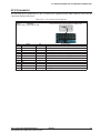
1
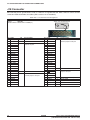
CMOS 16-BIT SINGLE CHIP MICROCOMPUTER
S5U1C17801T1100
Hardware Manual
(Software Evaluation Tool for S1C17801)
NOTICE
No part of this material may be reproduced or duplicated in any form or by any means without the written permission
of Seiko Epson. Seiko Epson reserves the right to make changes to this material without notice. Seiko Epson does
not assume any liability of any kind arising out of any inaccuracies contained in this material or due to its application
or use in any product or circuit and, further, there is no representation that this material is applicable to products requiring high level reliability, such as medical products. Moreover, no license to any intellectual property rights is granted by implication or otherwise, and there is no representation or warranty that anything made in accordance with this
material will be free from any patent or copyright infringement of a third party. This material or portions thereof may
contain technology or the subject relating to strategic products under the control of the Foreign Exchange and Foreign
Trade Law of Japan and may require an export license from the Ministry of Economy, Trade and Industry or other approval from another government agency.
Windows 2000 and Windows XP are registered trademarks of Microsoft Corporation, U.S.A.
PC/AT and IBM are registered trademarks of International Business Machines Corporation, U.S.A.
All other product names mentioned herein are trademarks and/or registered trademarks of their respective owners.
© SEIKO EPSON CORPORATION 2008, All rights reserved.
Configuration of product number
Devices
S1
C
17xxx
F
00E1
00
Packing specifications
00 : Besides tape & reel
0A : TCP BL
2 directions
0B : Tape & reel BACK
0C : TCP BR
2 directions
0D : TCP BT
2 directions
0E : TCP BD
2 directions
0F : Tape & reel FRONT
0G : TCP BT
4 directions
0H : TCP BD
4 directions
0J : TCP SL
2 directions
0K : TCP SR
2 directions
0L : Tape & reel LEFT
0M : TCP ST
2 directions
0N : TCP SD
2 directions
0P : TCP ST
4 directions
0Q : TCP SD
4 directions
0R : Tape & reel RIGHT
99 : Specs not fixed
Specification
Package
D: die form; F: QFP, B: BGA
Model number
Model name
C: microcomputer, digital products
Product classification
S1: semiconductor
Development tools
S5U1
C
17000
H2
1
00
Packing specifications
00: standard packing
Version
1: Version 1
Tool type
Hx : ICE
Dx : Evaluation board
Ex : ROM emulation board
Mx : Emulation memory for external ROM
Tx : A socket for mounting
Cx : Compiler package
Sx : Middleware package
Corresponding model number
17xxx: for S1C17xxx
Tool classification
C: microcomputer use
Product classification
S5U1: development tool for semiconductor products
TABLE OF CONTENTS
- Table of Contents 1 Features.......................................................................................................................... 1
2 Contents of Package ..................................................................................................... 2
3 Name and Functions of Each Part ............................................................................... 3
Name of Each Part ................................................................................................................... 3
CPU Board Dimensions ................................................................................................ 7
ICD Board Dimensions ................................................................................................. 8
LCD Board Dimensions ................................................................................................ 9
LCD Panel Board Dimensions ..................................................................................... 10
Main Parts ............................................................................................................................... 11
Functions of Each Part ............................................................................................................ 12
ICD Board .................................................................................................................... 12
CPU Board ................................................................................................................... 12
4 Block Diagram .............................................................................................................. 14
5 Operating Environments and Starting Procedures ................................................... 15
Software Simple Development Environments ......................................................................... 15
Standalone Operation of SVT17801 ....................................................................................... 18
ICD Board Firmware Update Procedures ............................................................................... 18
6 Difference between ICD Board and ICD Mini ............................................................. 19
7 I/O Port........................................................................................................................... 20
8 Jumper Switch Settings ............................................................................................... 22
Setting for JP1......................................................................................................................... 22
Setting for JP2......................................................................................................................... 23
Setting for JP3......................................................................................................................... 24
9 Connection Circuit to External Memory ..................................................................... 25
SRAM Connection Circuit ....................................................................................................... 25
NOR Flash Connection Circuit ................................................................................................ 26
NAND Flash Connection Circuit .............................................................................................. 27
EEPROM Connection Circuit .................................................................................................. 28
10 Power Control Circuit for Battery Backup Function ............................................... 29
Battery Backup Function ......................................................................................................... 29
Power Control Circuit for Battery Backup Function ................................................................. 29
11 LCD Panel Connection Circuit................................................................................... 32
Touch Panel Controller Connection Circuit ............................................................................. 33
12 Key Input Circuit on CPU Board ............................................................................... 34
13 Rotary Encoder Connection Circuit.......................................................................... 35
14 Tri-color LED Connection Circuit .............................................................................. 36
15 LED/LCD Backlight Control Circuit with MFT0 ........................................................ 37
16 Infrared Emitting Diode/Receiving Module Connection Circuit ............................. 38
Emitting and Receiving from/by Infrared Area......................................................................... 39
17 MMC (Multi-Media Card) Connection Circuit .............................................................. 40
18 USB Connection Circuit ............................................................................................. 41
S5U1C17801T1100 HARDWARE MANUAL
(SOFTWARE EVALUATION TOOL FOR S1C17801)
EPSON
i
TABLE OF CONTENTS
19 Audio Connection Circuit .......................................................................................... 42
Switching Audio Master Clock ................................................................................................. 42
20 Exclusive Control of Ports......................................................................................... 43
21 Serial ............................................................................................................................ 44
22 Specifications For Cpu Board Connectors .............................................................. 45
J6 Connector (to Connect with ICD) ....................................................................................... 45
J7 Connector ........................................................................................................................... 46
J8 Connector ........................................................................................................................... 47
J12 Connector ......................................................................................................................... 48
J13 Connector ......................................................................................................................... 49
J18 Connector ......................................................................................................................... 50
Appendix A How to Measure Current Consumption .................................................... 51
A.1 Measuring VDD Current Consumption .............................................................................. 51
A.2 Measuring AVDD Current Consumption ............................................................................ 52
A.3 Measuring RTCVDD Current Consumption ...................................................................... 52
ii
EPSON
S5U1C17801T1100 HARDWARE MANUAL
(SOFTWARE EVALUATION TOOL FOR S1C17801)
1 FEATURES
1 Features
S5U1C17801T1100 (Software eValuation Tool for S1C17801. Hereafter referred to as SVT17801)is an evaluation
board for MCU S1C17801 manufactured by SEIKO EPSON.
The SVT17801, consisting of the three boards, i.e., CPU, ICD and LCD, can debug software by connecting to
the ICD and CPU boards without using ICD or other debug tool. By connecting to the CPU and LCD boards, the
SVT17801 can also be used for simple evaluation of LCD panel display.
In addition, serial port, AD input port, and other expansion interfaces built in the SVT17801 allow customer s original
expansion boards to connect with the SVT17801.
〈CPU Board〉
CPU
Input power voltage
Regulator output voltage
CPU Input Clock
Built-in Functions/Devices
〈ICD Board〉
Interface with PC
Supply voltage
Built-in Functions/Devices
〈LCD board〉
LCD panel module
S1C17801
+5.0V (DC)
+3.3V
OSC1:32.768kHz
OSC3:48MHz
- Reset switch
- Expansion interface connectors (LCD, GPIO, UART, I2C, AD)
- ICD board connector
• SRAM (16Mbit)
• NOR Flash (64Mbit)
• NAND Flash (2Gbit)
• EEPROM (256Kbit)
- Battery backup control circuit/Power switch
- Key input circuit (6 keys)
- Rotary encoder with switch
- Status display LED (tri-color LED/mono-color LED x 2)
- Infrared LED/Receiver module
- AudioCodec
- USB miniB type connector
- MMC card socket
USB 1.1
USB bus power (On-board regulator output voltage of 3.3V)
- Status display LED (tri-color)
- Reset switch
- CPU board connector
3.5 inch STN QVGA 320 x 240 dots B&W panel
Membrane type touch panel
S5U1C17801T1100 HARDWARE MANUAL
(SOFTWARE EVALUATION TOOL FOR S1C17801)
EPSON
1
2 CONTENTS OF PACKAGE
2 Contents of Package
The following lists the contents of S5U1C17801T1100 package:
(1)
(2)
(3)
(4)
(5)
(6)
(7)
(8)
(9)
(10)
2
SVT17801 CPU Board (Main body) .......................... 1
SVT17801 ICD Board ................................................. 1
SVT17801 LCD Board ................................................ 1
USB Cable .................................................................... 1
Coin Battery (CR2032/3V) ......................................... 1
AC Adapter .................................................................. 1
Warranty Registration Card ....................................... 1 each for English/Japanese
Warranty Card............................................................. 1 each for English/Japanese
Precautions in Use ....................................................... 1 each for English/Japanese
Manual Download Guide............................................ 1 each for English/Japanese
EPSON
S5U1C17801T1100 HARDWARE MANUAL
(SOFTWARE EVALUATION TOOL FOR S1C17801)
3 NAME AND FUNCTIONS OF EACH PART
3 Name and Functions of Each Part
Name of Each Part
The following describes name and functions of each part:
ICD board
(4)
(2)
(5)
(3)
(8)
(6)
(1)
(9)
(7)
(10)
CPU board
(5)
(9)
3.5inch
STN QVGA B&W
(11)
Membrane touch panel
(12)
(15) (14)
(16)
(13)
(9)
Fig. 3.1.1 Name of Each Surface Mounted Part (with LCD Panel)
(1)
(2)
(3)
(4)
(5)
(6)
Power LED (Blue)
Speaker (Left)
RESET SW
USBminiB connector
LED (RGB)
MIC
(7) LED
(8) POWER SW
(9) GND pin
(10) Speaker (Right)
(11) JP pin
(12) Expansion connector
S5U1C17801T1100 HARDWARE MANUAL
(SOFTWARE EVALUATION TOOL FOR S1C17801)
EPSON
(13)
(14)
(15)
(16)
Key switch
Crystal oscillator (48MHz/32KHz)
S1C17801
LCD board
3
ICD board
3 NAME AND FUNCTIONS OF EACH PART
CPU board
(1)
(2)
(3)
(4)
(5)
Fig. 3.1.2 Name of Each Surface Mounted Part (without LCD Panel)
(1) Infrared emitting module LED
(2) FLASH (NOR)
4
(3) SRAM
(4) FLASH (NAND)
EPSON
(5) Expansion connector (LCD board)
S5U1C17801T1100 HARDWARE MANUAL
(SOFTWARE EVALUATION TOOL FOR S1C17801)
3 NAME AND FUNCTIONS OF EACH PART
ICD board
(4)
(6)
(1)
(7)
(2)
(3)
(5)
(3)
(8)
CPU board
(9)
(10)
(19)
(16)
(18)
(17)
(14)
(12)
(11)
(13)
(15)
Fig. 3.1.3 Name of Each Rear Face Mounted Part
(1)
(2)
(3)
(4)
(5)
Rotary encoder with Switch
RESET SW
ICDminiI/F
ICD board connector
Placement of infrared receiver
module (substitute)
(6) Audio connector (OUT)
(7) Audio connector (IN)
(8) Power supply connector (5V)
(9) AudioCodec
(10) Power Switch
(11) AudioCodec Oscillator
(12) MMC Card Socket
(13) Infrared receiver module
S5U1C17801T1100 HARDWARE MANUAL
(SOFTWARE EVALUATION TOOL FOR S1C17801)
EPSON
(14) GND pin
(15) USBminiB connector
(16) Bus connector (Not available)
(17) Coin Battery
(18) Measuring JP for IC consumed
current
(19) EEPROM
5
3 NAME AND FUNCTIONS OF EACH PART
(1)
(2)
Fig. 3.1.4 Name of Each Part Mounted on Rear Face of LCD Board
(1) Connector (to connect LCD panel)
(2) Connector (to connect CPU board)
6
EPSON
S5U1C17801T1100 HARDWARE MANUAL
(SOFTWARE EVALUATION TOOL FOR S1C17801)
3 NAME AND FUNCTIONS OF EACH PART
Board Dimensions
CPU Board Dimensions
The following drawing shows dimensions of the CPU board.
<Surface>
Parts installed within this dash line must be max. 8 mm in height
205
170
142
D1 Installation instruction diagram
85
11
12
SP1
2
63
2
1 2
40
1
J7
22
1
J12
2
46.5
1
8 10.5
17
J8
1516
53
S1 S2 S3
17 18
26.5
112
55
50
20
7
S4 S5 S6
2
5.5
10
SP2
137
50
90
89
80
100
102.5
S7
D1
J13
1
9
10
7.5
1
46
25
9
102
9
9-φ7
9-φ3.3 hole
167
4
197
<Rear Face>
185
155
140
110
72.5
10
B
C
S
A
9
2
J6
1
3 1
U21
1
4
31
2
2
6
10
4 1 1
4
J11
J9
3
J14
2
4
1.5
15
4
8.2
2 1
S8
37.5
2
1J43
J15
3
1
J5
912345678
BAT1
SW1
32
50
55
67.5
SW2
10.5
2.7
15
4
4
J10
1 5
U23
1 3
(CARD CENTR)
52.5
9-φ7
80
110
155
Fig. 3.2.1.1 CPU Board Dimensions
∗ Precautions
• Unit for the above dimensions is millimeter (mm).
• Board thickness: 1.6 mm, U23 is not mounted.
S5U1C17801T1100 HARDWARE MANUAL
(SOFTWARE EVALUATION TOOL FOR S1C17801)
EPSON
7
3 NAME AND FUNCTIONS OF EACH PART
ICD Board Dimensions
The following drawing shows dimensions of the ICD board.
<Parts Side View>
R
4-
4-φ3.5 through hole
5.5
21.5
43
37.5
5 1
2
JUSB
4
4
9
4-φ7 land
50
<Soldering Side View>
2
1
10
9
JICD
4.95
Fig. 3.2.2.1 ICD Board Dimensions
∗ Precautions
• Unit for the above dimensions is millimeter (mm).
• Material: FR4, Board thickness: 1.6 mm
8
EPSON
S5U1C17801T1100 HARDWARE MANUAL
(SOFTWARE EVALUATION TOOL FOR S1C17801)
3 NAME AND FUNCTIONS OF EACH PART
LCD Board Dimensions
The following drawing shows dimensions of the LCD board.
<Surface>
112
10
5
6-φ3.3(NTH)
80
5
15
10
65.5
90
3
5
19
20
51
5
51
<Rear Face (View from Surface)>
102
26
6-φ7
55
6-φ3.3 hole
1
3
1
17
18
1
J101
2
5
15
20
(Hole)
65.5
J103
10
50
J104
70.5
50
90
14
29
4
2
J102
80
12
1
10
11
19
5
20
51
51
112
Fig. 3.2.3.1 LCD Board Dimensions
∗ Precautions
• Unit for the above dimensions is millimeter (mm).
• Board thickness: 1.6 mm
• Figure 3.2.3.1 is a rear face drawing seen from the board surface.
S5U1C17801T1100 HARDWARE MANUAL
(SOFTWARE EVALUATION TOOL FOR S1C17801)
EPSON
9
3 NAME AND FUNCTIONS OF EACH PART
LCD Panel Board Dimensions
The following drawing shows dimensions of the LCD panel (EW32F92FLWP manufactured by IMAGING DISPLAY).
(Abstracted from specifications for the IMAGING DISPLAY EW32F92 series products)
30.0
96.2
91.3(touch panel)
81(viewing area of touch panel)
79(active area of touch panel)
77.79±0.3(viewing area of bezel)
79.79±0.01(display area)
6.3
7.3
7.9
8.405
72
66.6
60(viewing area of touch panel)
58.59±0.3(viewing area of bazel)
58(active area of touch panel)
57.59±0.01(display area)
TOP
IF2
60.9
RIGHT
”A”
LEFT
10±2(STIFFER)
BOTTOM
27.8±5
2.2
4
4.7
(5.0)
5.205
0.6
IF1
15
13(P1.0*13),W=0.7
0.3±0.05
7±1(STIFFER)
7.1
4.3
CONTACT SIDE
4.0±0.3
CONDUCTOR
UNIT : mm
SCALE : NTS
NOT SPECIFIED TOLERANCE IS ±0.5
0.3
0.65±0.1
2-R0.3
5±0.1
14±1
1±0.1
9.3 Max.
5
1
CONTACT SIDE
VIEWING DIRECTION
6.2
1.4
PIN1
A DETAIL
Fig. 3.2.4.1 LCD Panel Dimensions
10
EPSON
S5U1C17801T1100 HARDWARE MANUAL
(SOFTWARE EVALUATION TOOL FOR S1C17801)
3 NAME AND FUNCTIONS OF EACH PART
Main Parts
<CPU Board>
CPU (U13)
Crystal oscillator (32.768kHz) (X1)
Crystal oscillator (48MHz) (X2)
Reset switch (RESET SW) (S8)
Expansion connector (J7)
Expansion connector (J8)
Expansion connector (J12)
Expansion connector (J13)
ICD board connector (J6)
SRAM (U18)
Flash(NOR) (U3)
Flash(NAND) (U7)
EEPROM (U17)
POWER SW (S7)
Key switches (S1 - S6)
Rotary encoder with switch (SW2)
LED(RGB) (LED1)
Power LED (Blue) (LED2)
LED (LED3)
Infrared emitting module (D1)
Infrared receiver module (U21)
Infrared receiver module (for U21)
AudioCodec (U22)
AudioCodec Oscillator (OSC1)
Audio connector (J14)
Audio connector (J15)
Speakers (SP1, SP2)
MIC (MIC1)
USB miniB connector (J10)
MMC card socket (J5)
Battery holder (BAT1)
Coin Battery
Power supply connector (5V) (J4)
Power Switch (SW1)
ICDmini i/f (J9)
ICDmini i/f (J11)
S1C17801
FC-135
FA-238
SKQTLCE010
SSW-109-01-S-D
SSW-108-01-S-D
TSW-109-07-S-D
TSW-106-07-S-D
PS-10SD-D4T1-1
CY62167DV30LL-55ZXI
S29JL064H55TFI000
MT29F2G08AACWP
24AA256-I/SN
SKRAAKE010
SKRAAKE010
SIQ-02FVS3
598-9920-307F
598-8191-107F
LTW-170TK
AN333
GP1UX311QS
PNA4702M
PCM3793ARHB
SG-8002JC-12.288M-PCCB
SJ-43514-SMT
SJ-3523-SMT
NDT-03B
EM6022P-42BC10&33-G
54819-0578
DM1B-DSF-PEJ(22)
106
CR2032 (3V)
HEC3600-010510
SDDJE12300
A2-4PA-2.54DS (71)
S04B-PASK-2 (LF) (SN)
SEIKO EPSON CORP.
EPSON TOYOCOM CORP.
EPSON TOYOCOM CORP.
ALPS
SAMTEC
SAMTEC
SAMTEC
SAMTEC
JAE
CYPRESS
Spansion
MICRON
ST-Micro
ALPS
ALPS
MITSUMI
Dialight
Dialight
Lite-On
STANLEY
SHARP
Panasonic
TI
EPSON TOYOCOM CORP.
CUI Inc
CUI Inc
STAR MICRONICS
Horn Industrial
molex
HIROSE
KEYSTONE
maxell
Hosiden
ALPS
HIROSE
JST
54819-0572
598-9920-307F
SKRAAKE010
molex
Dialight
ALPS
EW32F92FLWP
DF9-13P-1V(32)
DF9-9P-1V(32)
52207-1485
52207-0485
IMAGING DISPLAY
HIROSE
HIROSE
Molex
Molex
<ICD Board>
USB miniB type connector
LED (RGB)
Reset switch (RESET SW) (SW1)
<LCD board>
LCD panel module
Connector (to connect CPU board) (J101)
Connector (to connect CPU board) (J102)
Connector (to connect LCD panel) (J103)
Connector (to connect LCD panel) (J104)
S5U1C17801T1100 HARDWARE MANUAL
(SOFTWARE EVALUATION TOOL FOR S1C17801)
EPSON
11
3 NAME AND FUNCTIONS OF EACH PART
Functions of Each Part
ICD Board
The ICD board is a hardware tool (emulator) to facilitate the efficiency of software development for the S1C17801.
It controls communication between your PC and the target IC (S1C17801) on the CPU board, providing simple
software development environments for S1C17801. For information about its functional difference from the ICD
Mini (S5U1C17001H), a development tool supporting all S1C17 core product models, see Chapter 6.
ICD Board Reset Switch
Pressing the reset switch (SW1) on the ICD board reboots firmware on the ICD board and outputs the target
reset signal (#RESET_OUT) to the CPU board. This establishes the communication connection between the
CPU board and the ICD board if they are physically connected. If the CPU board and the ICD board are not
connected physically, the communication connection becomes in the stand-by status.
ICD Board LED
The LED indicates ICD board and target statuses in different colors.
● (Blue) Power on (before the initial connection with the target is established.)
● (Green) The target is currently in debug mode.
● (Red) The target is not connected, or not properly connected.
The target is currently executing a user program.
CPU Board
The CPU board is a simple target evaluation board equipped with the target CPU (S1C17801). It is also equipped
with SRAM, NOR Flash, NAND Flash, EEPROM and other external memories,as well as peripheral functions and
circuits such as a LCD panel, RTC control circuit, MMC card, USB Audio IC, speaker, microphone, and remote
control emitting/receiving module, enabling the CPU board to be used for the development and evaluation of control software and other purpose.
CPU Board Reset Switch
Pressing the reset switch on the CPU board (S8 mounted on the rear face) resets the CPU board.
Coin Battery
A coin cell battery (of CR2032 standard) socket is mounted on the rear face of the CPU board. The socket is
used for power supply to RTCVDD.
12
EPSON
S5U1C17801T1100 HARDWARE MANUAL
(SOFTWARE EVALUATION TOOL FOR S1C17801)
3 NAME AND FUNCTIONS OF EACH PART
∗ Installing and Removing Coin Battery
The following describes installation and removal procedures of a coin cell to/from the socket on the rear
face of the CPU board.
Install Step 1: Insert coin cell under the long metal contact on the socket with the plus (+) side up, and press it
in the direction of the arrow.
Fig. 3.4.2.1 Installing/Removing Coin Battery - 1/4
Install Step 2: Figure 3.4.2.2 shows the installation has been completed.
Fig. 3.4.2.2 Installing/Removing Coin Battery - 2/4
Remove Step 1: Insert a slotted screw driver into space between the coin cell and socket, lift the driver up as
a lever and move it in the direction of arrow to secure a small space on the right side of the
socket as shown in the figure 3.4.2.3.
Fig. 3.4.2.3 Installing/Removing Coin Battery - 3/4
Remove Step 2: Insert the slotted driver into the space on the right side as shown in the figure 3.4.2.4. Then
pressing it to the right removes the coin cell. (The cell can also be removed by lifting the driver
up as a lever.)
Fig. 3.4.2.4 Installing/Removing Coin Battery - 4/4
S5U1C17801T1100 HARDWARE MANUAL
(SOFTWARE EVALUATION TOOL FOR S1C17801)
EPSON
13
4 BLOCK DIAGRAM
4 Block Diagram
Each block diagram for the the SVT17801 CPU board and ICD board is shown below.
<CPU Board>
ICDmini
ICD mini connector
Debug i/f
ICD
connector
3-color LED x1
GPIO
Debug i/f
Card i/f
OSC1
32kHz
OSC3
48MHz
NAND FLASH
USB
USBminiB
USB 2.0(FS)
SPI
SD Card I/f
SD Card
RTC
+RAM
Coin
Cell
Speaker
Reset
RESET (SW)
Audio
AD/DA
I 2S
ADx
I/O connector
ADx
LED
Infrared LED
ADx
Bus
Audio input
FLASH
UART
LCD panel connector
GPIO
ADx
ADx
GPIO
SRAM
GPIO
LCDC
REMC communi cation
External Device
I 2C
MFT0
SW
Receiving module
REMC
ADx
Regul ator
5V→3.3V
5V DC
SW
Microphone
Audio jack
ADx
EPPROM
Audio output
Audio jack
Rotary switch
Bus connector
(Not available)
ICD board
Key(6)
ADx
CPU board
100V AC
B& W QVGA LCD Panel
Module
Touch panel control LCD
board
Fig. 4.1 Block Diagram for CPU Board
<ICD Board>
USB 1.1
Host PC
CPU Board
USB1.1
5V
OSC3
500mA 48MHz
Max.
S1C33E07
Flash ROM
Regulator
5V->1.8V
Regulator
5V->3.3V
3-color
LED x1
Fig. 4.2 Block Diagram for ICD Board
14
EPSON
S5U1C17801T1100 HARDWARE MANUAL
(SOFTWARE EVALUATION TOOL FOR S1C17801)
5 OPERATING ENVIRONMENTS AND STARTING PROCEDURES
5 Operating Environments and Starting
Procedures
By connecting with your PC via the ICD board, the SVT17801 can be operated in accordance with commands executed by a debugger on the PC. The SVT17801 CPU board can be operated as stand-alone without using the ICD
board and PC. The following explains the connection and starting procedures required for each operation.
Software Simple Development Environments
The SVT17801 can provide simple development environments of software using the CPU board as a target. This
can be achieved by connecting the SVT17801 to your PC via the ICD board and using the S1C17 development tool
on the PC (such as GNU17 IDE, compiler and debugger included in the S5U1C17001C package).
S5U1C17001C
(Debugger)
USB cable
ICD
board
AC power adapter
C17801
B/W QVGA
LCD panel module
CPU board
Fig. 5.1.1 Software Simple Development Environments
Operation under Software Simple Development Environments
Under these operating environments,the target CPU (the S1C17801 on the CPU board) operates according to
commands executed by a debugger on your PC connected with the ICD board. A command executed by the
debugger is sent to the ICD board via USB to be analyzed and converted into a debug signal, and then sent
to the CPU board. The debugger on your PC can be used to download programs or data to the CPU board, or
debug programs by controlling their execution and stop.
Operating Mode of CPU
The "brk" command or debugging interrupts (such as forcible breaking operation by the debugger) from the
ICD board causes the target CPU (the S1C17801 on the CPU board) to stop executing the target program and
enter into debug mode (or break status). In this status, commands can be executed from the debugger on your
PC. LED on the ICD board lights in green during debug mode. On the other hand, the status where the target
CPU executes the target program is called normal mode. LED on the ICD board lights in red during normal
mode.
Connection and Start
The following describes connection and startup procedures to allow for the software simple development
environments.
(1) Connect the ICD board with the CPU board. Connect JICD 10 pin connector on the ICD board with the
counterpart on the CPU board. Then turn on the CPU board.
S5U1C17801T1100 HARDWARE MANUAL
(SOFTWARE EVALUATION TOOL FOR S1C17801)
EPSON
15
5 OPERATING ENVIRONMENTS AND STARTING PROCEDURES
(2) Turn on the PC (if it is turned off).
(3) Connect the evaluation board to your PC via a USB cable.
(4) When a screen appears on your PC prompting you to install USB driver, install an appropriate driver. This
operation is required only for the first connection. It is not required for the second connection and afterward. For the installation procedure, see the later section Installing USB driver .
(5) Make sure that LED on the ICD board lights in blue → green (the target is in debug mode).
(6) Start the debugger on your PC to execute the program. Make sure that LED on the ICD board lights in red (the
target is in normal mode).
For details on the operation of the debugger and debugging commands, see the S5U1C17001C Manual (S1C17
Family C Compiler Package).
Note: Be sure never to disconnect a USB cable between PC and ICD board while the debugger is running.
Installing the USB driver
(1) When the SVT17801 is connected with the host computer via USB cable, the following screen appears.
(2) Follow the wizard to install USB driver.
For brows directory of the USB driver, specify C:\EPSON\GNU17\utility\drv_usb.
∗ This indicates a directory path where IDE is installed.
16
EPSON
S5U1C17801T1100 HARDWARE MANUAL
(SOFTWARE EVALUATION TOOL FOR S1C17801)
5 OPERATING ENVIRONMENTS AND STARTING PROCEDURES
When the USB driver has been installed successfully,it appears on the device manager as shown below.
Notes: If the driver does not appears on the device manager as shown above, install the USB driver again.
S5U1C17801T1100 HARDWARE MANUAL
(SOFTWARE EVALUATION TOOL FOR S1C17801)
EPSON
17
5 OPERATING ENVIRONMENTS AND STARTING PROCEDURES
Standalone Operation of SVT17801
The SVT17801 CPU board can be operated as stand-alone without using the ICD board and PC.
Standalone Operation
In this operation environment, the S1C17801 on the CPU board operates in normal mode to execute a program
written in the built-in flash memory. Therefore, a user program must be downloaded previously to the flash
memory built in the S1C17801. (A demo-program is written in the flash memory of the SVT17801 as factory
default.)
For information about how to download a user program to the memory, see the "S5U1C17001C Manual (S1C17
Family C Compiler Package)."
Connection and Start
The following describes a method to operate the SVT17801 as standalone.
(1) Turn on the PC (if it is turned off).
(2) While the ICD board is connected with the CPU board, connect your PC to the ICD board via USB cable,
and turn on the CPU board.
(3) Start the debugger on your PC and download a user program to the flash memory built in the S1C17801.
For information about downloading a program, see the S5U1C17001C Manual (S1C17 Family C Compiler
Package).
(4) After exiting the debugger, remove the USB cable to disconnect the ICD board from your PC.
(5) Disconnect the ICD board from the CPU board, and install a coin cell battery.
(6) Press the reset switch on the CPU board. Then the S1C17801 on the CPU board starts executing a user program downloaded to the flash memory.
ICD Board Firmware Update Procedures
The SVT17801 can update the firmware of the ICD board using the debugger on your PC. The ICD board firmware
will be provided by EPSON if necessary. An update file has an .sa extension.)
The following describes firmware update procedures.
Note: USB driver must be installed before starting firmware update.
(1) Connect the evaluation board to your PC via a USB cable.
(2) Press the reset switch on the CPU board.
(3) Start the debugger from the command prompt.
>cd c:\EPSON\gnu17
(Specify the directory path where the gnu17 is installed.)
>gdb
(4) When the debugger starts, enter the following commands.
(gdb) target icd usb
(gdb) c17 firmupdate path\filename.sa
(where path\filename.sa is the update file name.)
(5) Finally, when the LED on the ICD board gets green(●), the firmware has been updated.
(6) Press the reset switch on the ICD board to reboot the firmware.
18
EPSON
S5U1C17801T1100 HARDWARE MANUAL
(SOFTWARE EVALUATION TOOL FOR S1C17801)
6 DIFFERENCE BETWEEN ICD BOARD AND ICD MINI
6 Difference between ICD Board and
ICD Mini
The table 6.1 shows specifications comparison between the SVT17801 ICD board and the S5U1C17001H (ICD
Mini), a development tool for the S1C17 Family. While the SVT17801 is equipped with the ICD mini interface, the
ICD board and the ICD mini cannot be connected at the same time. For information about how to use the ICD mini,
refer to the S5U1C17001H User Manual.
Table 6.1 Comparison of Functions between ICD Board and ICD mini
Product name
S5U1C17000H
ICD mini
SVT17701 (S5U1C17001T)
ICD board
S1C17 core
USB 1.1
Approx. 65KB/s DCLK = at 40MHz (Max.) ∗1
Approx. 50KB/s DCLK = at 20MHz ∗1∗4
4KHz - 40MHz
Corresponding core
Host interface
Maximum speed of data download
Communications frequency with target
(DCLK frequency)
Standalone flash writer function
Available
Firmware update function
Power supply for writing to flash ROM
Reset signal output to target
Target system I/O support voltage
Connector to connect target
None
Available
Available
Available
3.3V, 1.8V, and voltage input from
target (1.0 - 5.0V)
4 pins
Power supply connector for writing to
flash ROM ∗3
4 pins
None
3.3V
10 pins
(including reset signal) ∗2
–
∗1 Supported frequency when I/O interface voltage = 3.3V Depending on ambient noise, temperature conditions, and
types and variations of products,
the maximum frequency may become lower than the specification value.
∗2 Only for connection with the CPU board.
∗3 Separate power supply is not required for the S1C17801 to write to flash ROM.
∗4 Operating frequency is 48MHz (DCLK=24MHz) for SVT17801.
S5U1C17801T1100 HARDWARE MANUAL
(SOFTWARE EVALUATION TOOL FOR S1C17801)
EPSON
19
7 I/O PORT
7 I/O Port
Table 7.1 lists ports on the S1C17801 and the destination of the connection for the SVT17801.
For information about expansion interface and connectors, see Chapter 22.
Table 7.1 I/O Port Function List
Port Direction
20
Multiplex
Signal Name
P00/AIN0
P01/AIN1
P02/AIN2
P03/AIN3
P04/AIN4
P05/AIN5
P06/AIN6
P07/AIN7
P10/SPI_SDI0
P11/SPI_SDO0
P12/SPI_SCK0
P13/SPI_SSI0/SPI_SSI1
P14/SPI_SDI1
P15/SPI_SDO1
P16/SPI_SCK1
P20/I2S_SDO0
P21/I2S_WS0
P22/I2S_SCK0
P23/I2S_MCLK0
P24/I2S_SDI1
P25/I2S_WS1
P26/I2S_SCK1
P27/I2S_MCLK1
P30/TM0
P31/#TM0/#ADTRG
P32/WDT_CLK/
#WDT_NMI/CMU_CLK
P33/#SMRD/#TM0
P34/#SMWR
P35/DCLK
P36/DSIO
P37/DST2
P40/SIN0/#SMRD
P41/SOUT0/#SMWR
P42/#SCLK0/EXCL0
P43/REMC_IN/PWMPRT0
P44/REMC_OUT
P45/#WAIT
P50/I2C_SDA/EXCL0
P51/I2C_SCL
P52/REMC_IN/#TM0
P53/REMC_OUT
P55/FPLINE
P56/FPSHIFT/#TM0
P57/FPDRDY
P60/A0/#BSL
P61/A1
P00
P01
P02
P03
P04
P05
P06
P07
P10
P11
P12
P13
P14
P15
P16
P20
P21
P22
P23
P24
P25
P26
P27
P30
P31
P32
I
I
I
I
I
I
I
I
I/O
I/O
I/O
I/O
I/O
I/O
I/O
I/O
I/O
I/O
I/O
I/O
I/O
I/O
I/O
I/O
I/O
I/O
AIN0
AIN1
AIN2
AIN3
AIN4
AIN5
AIN6
AIN7
SPI0
SPI0
SPI0
SPI0/SPI1
SPI1
SPI1
SPI1
I2S0
I2S0
I2S0
I2S0
I2S1
I2S1
I2S1
I2S1
TM0
TM0/ADTRG
WDT/CMU
P33
P34
P35
P36
P37
P40
P41
P42
P43
P44
P45
P50
P51
P52
P53
P55
P56
P57
P60
P61
I/O
I/O
I/O
I/O
I/O
I/O
I/O
I/O
I/O
I/O
I/O
I/O
I/O
I/O
I/O
I/O
I/O
I/O
I/O
I/O
Memory/TM0
Memory
ICD i/f
ICD i/f
ICD i/f
UART/Memory
UART/Memory
UART/EXCL
REMC
REMC
WAIT
I2C/EXCL0
I2C
REMC/TM0
REMC
LCD
LCD
LCD
Memory
Memory
EPSON
Connected to
Expansion I/F (Connector No.: J8)
Expansion I/F (Connector No.: J13)
Key input
MMC I/F & TP52
MMC I/F & TP53
MMC I/F & TP54
MMC I/F & TP55
Tri-color LED
AudioCodecIC & TP49
AudioCodecIC & TP48
AudioCodecIC & TP47
AudioCodecIC
AudioCodecIC & TP50
AudioCodecIC & TP48
AudioCodecIC & TP47
AudioCodecIC & TP51
Switch IC → Uni-color LED
Rotary encoder & key input
Switch IC
Switch IC → NAND Flash or
expansion I/F (Connector No.: J13)
ICD I/F (Connector No.: J6)
Expansion I/F (Connector NO.: J8) & TP42
Expansion I/F (Connector NO.: J8) & TP43
Expansion I/F (Connector NO.: J8) & TP44
STBY(S1C17801)
NAND Flash & NOR Flash
Switch IC
Expansion I/F (Connector No.: J8) & EEPROM
Expansion I/F (Connector No.: J8) & EEPROM
Remote control light receiving module
Remote control light emitting module
Expansion I/F (Connector No.: J12)
Expansion I/F (Connector No.: J18) & SRAM
Expansion I/F (Connector No.: J18) & SRAM
S5U1C17801T1100 HARDWARE MANUAL
(SOFTWARE EVALUATION TOOL FOR S1C17801)
7 I/O PORT
Port Direction
Multiplex
Signal Name
Connected to
P62
P63
P64
P65
P66
P67
P70
P71
P72
P73
P74
P75
P76
P77
P80
P81
P82
P83
P84
P85
P86
P90
P91
P92
P93
P94
P95
P96
P97
PA0
PA1
PA2
PA3
PA4
PA5
PA6
PB0
PB1
PB2
PB3
PB4
PB5
PB6
PB7
PC0
PC1
PC2
PC3
I/O
I/O
I/O
I/O
I/O
I/O
I/O
I/O
I/O
I/O
I/O
I/O
I/O
I/O
I/O
I/O
I/O
I/O
I/O
I/O
I/O
I/O
I/O
I/O
I/O
I/O
I/O
I/O
I/O
I/O
I/O
I/O
I/O
I/O
I/O
I/O
I/O
I/O
I/O
I/O
I/O
I/O
I/O
I/O
I/O
I/O
I/O
I/O
Memory
Memory
Memory
Memory
Memory
Memory
Memory
Memory
Memory
Memory
Memory
Memory
Memory
Memory
Memory
Memory
Memory
Memory
Memory
Memory
Memory
Memory
Memory
Memory
Memory
Memory
Memory
Memory
Memory
Memory
Memory
Memory
Memory
Memory
Memory
Memory
Memory
Memory
Memory
Memory
Memory
Memory
Memory
Memory
LCD
LCD
LCD
LCD
P62/A2
P63/A3
P64/A4
P65/A5
P66/A6
P67/A7
P70/A8
P71/A9
P72/A10
P73/A11
P74/A12
P75/A13
P76/A14
P77/A15
P80/A16
P81/A17
P82/A18
P83/A19
P84/A20
P85/A21
P86/A22/CMU_CLK
P90/D0
P91/D1
P92/D2
P93/D3
P94/D4
P95/D5
P96/D6
P97/D7
PA0/#CE0
PA1/#CE1
PA2/#CE2
PA3/#CE3
PA4/#RD
PA5/#WRL
PA6/#WRH/#BSH
PB0/D8
PB1/D9
PB2/D10
PB3/D11
PB4/D12
PB5/D13
PB6/D14
PB7/D15
PC0/FPDAT0/CMU_CLK
PC1/FPDAT1/#WDT_NMI
PC2/FPDAT2/#ADTRG
PC3/FPDAT3/PWMPRT0
Expansion I/F (Connector No.: J18) &
SRAM & NOR Flash
PC4
PC5
PC6
PC7
I/O
I/O
I/O
I/O
LCD
LCD
LCD
LCD
PC4/FPDAT4
PC5/FPDAT5
PC6/FPDAT6
PC7/FPDAT7
S5U1C17801T1100 HARDWARE MANUAL
(SOFTWARE EVALUATION TOOL FOR S1C17801)
EPSON
Expansion I/F (Connector No.: J18) &
NOR Flash
Expansion I/F (Connector No.: J18) &
SRAM & NOR Flash & NAND Flash
NOR Flash
SRAM
NAND Flash
NAND Flash
NOR Flash & SRAM
NOR Flash & SRAM
SRAM
Expansion I/F (Connector No.: J18) &
SRAM & NOR Flash
Rotary encoder
Switch IC → NAND Flash or reset
Switch IC → NAND Flash or
expansion I/F (Connector No.: J8)
Expansion I/F (Connector No.: J12)
21
8 JUMPER SWITCH SETTINGS
8 Jumper Switch Settings
Three jumper switches are installed on the surface of the SVT17801. Each function is as follows:
Setting for JP1
JP1 can be used to select Wakeup Enable or Disable as shown in the following. 1-2 on JP1 must be shorted to select
Wakeup Enable. Wakeup Enable can be controlled by the Wakeup pin on the S1C17801 or on-board power switch.
For details, see the description of RTC control circuit in Chapter 10. Shorting 2-3 on JP1 disables the Wakeup function.
Factory default setting for JP1 is Wakeup Enable.
To 3.3V regulator
To POWER SW
U24
SN74LVC1G98DCKR
1
6
G
JP1
V
2
5
G
C49
+5V
0.1µF
1
JP1
JP1
2
3
DIC-149-3P
R59
10K
Q11
UNR5213
DISABLE WAKEUP
4
ENABLE WAKEUP
3
To WAKEUP pin
Fig. 8.1.1 JP1 Related Circuit
22
EPSON
S5U1C17801T1100 HARDWARE MANUAL
(SOFTWARE EVALUATION TOOL FOR S1C17801)
8 JUMPER SWITCH SETTINGS
Setting for JP2
JP2
JP2
JP2
Battery
VDD
VDD
JP2 can be used to select the power supply source for RTCVDD as shown in the following. Short 2-3 on JP2 to select VDD for the power supply to RTCVDD, whereas 1-3 to select battery. For details, see the description of RTC
control circuit in Chapter 10. Note that, when 1-2 is shorted, a coin cell battery is required to activate RTCVDD.
Factory default setting for JP2 is 1-2 shorted.
3
2
To RTCVDD
1
DIC-149-3P
C55
0.1µF
C47
10µF
1
D10
CRS06
+
BAT1
106
2
–
Fig. 8.2.1 JP2 Related Circuit
S5U1C17801T1100 HARDWARE MANUAL
(SOFTWARE EVALUATION TOOL FOR S1C17801)
EPSON
23
8 JUMPER SWITCH SETTINGS
Setting for JP3
JP3 wiring, allowing for three functions, is shown in the following.
∗ 1-2 Shorted
Power is supplied to LCD backlight. Shorting 3-4 is not allowed while 1-2 is shorted.
∗ 3-4 Shorted
Power with phase generated by.MFT0 on the S1C17801 is supplied to LCD backlight. It can be used to adjust the
brightness of LCD backlight. Shorting 1-2 is not allowed while 2-3 is shorted. For details, see Chapter 15 LED/
LCD BACKLIGHT CONTROL CIRCUIT WITH MFT0.
∗ 5-6 Shorted
Power with phase generated by MFT0 is supplied to LED3. It can be used to adjust the brightness of LED3. Either 1-2 or 2-3 can be shorted while 5-6 is shorted. For details, see Chapter 15 LED/LCD BACKLIGHT CONTROL CIRCUIT WITH MFT0.
Factory default setting for JP3 is 1-2 and 5-6 shorted.
VDD
VDD
JP3
VLSS (LCD module)
1
2
3
4
5
6
U20
TS5A3166
1
2
4
DIC-152-6P
R90
470
V
5
3
G
MFT0
C65
0.1µF
JP3
LED3
LTW-170TK
LCD_BL_ON
LCD_BL_PWM
D201_PWM
Fig. 8.3.1 JP3 Related Circuit
24
EPSON
S5U1C17801T1100 HARDWARE MANUAL
(SOFTWARE EVALUATION TOOL FOR S1C17801)
9 CONNECTION CIRCUIT TO EXTERNAL MEMORY
9 Connection Circuit to External Memory
SRAM, NOR Flash, NAND Flash, and EEPROM are connected to the SVT17801 as external memory modules.
SRAM Connection Circuit
CYPRESS 16M bits SRAM (CY62167DV30) is installed on the SVT17801. The following diagram shows how the
EEPROM is connected to the SVT17801.
S1C17801
CY62167DV30
A1 to A20
D0 to D15
25
24
23
22
21
20
19
18
8
7
6
5
4
3
2
1
48
17
16
9
10
13
R20
R19
R15
R73
10K
10K
10K
10K
VDD
A1
A2
A3
A4
A5
A6
A7
A8
A9
A10
A11
A12
A13
A14
A15
A16
A17
A18
A19
A20
12
26
28
11
14
15
CE1
RD
WRL
WRH/RSH
A0/BSL
A0
A1
A2
A3
A4
A5
A6
A7
A8
A9
A10
A11
A12
A13
A14
A15
A16
A17
A18
A19
D0
D1
D2
D3
D4
D5
D6
D7
D8
D9
D10
D11
D12
D13
D14
D15/A-20
NC
DNU
CE2
CE1
OE
WE
BHE
BLE
29
31
33
35
38
40
42
44
30
32
34
36
39
41
43
45
D0
D1
D2
D3
D4
D5
D6
D7
D8
D9
D10
D11
D12
D13
D14
D15
VDD
VCC
VSS
VSS
BYTE
37
46
27
C11
0.1µF
R11
10K
47
Fig. 9.1.1 SRAM Connection Circuit
S5U1C17801T1100 HARDWARE MANUAL
(SOFTWARE EVALUATION TOOL FOR S1C17801)
EPSON
25
9 CONNECTION CIRCUIT TO EXTERNAL MEMORY
NOR Flash Connection Circuit
SPANION 64M bits NOR Flash (S29JL064H) is installed on the SVT17801. The following diagram shows how the
EEPROM is connected to the SVT17801.
S1C17801
A1 to A22
D0 to D15
R8
R9
R10
10K
10K
10K
VDD
CE0
RD
WRL
P44
RESET
A1
A2
A3
A4
A5
A6
A7
A8
A9
A10
A11
A12
A13
A14
A15
A16
A17
A18
A19
A20
A21
A22
25
24
23
22
21
20
19
18
8
7
6
5
4
3
2
1
48
17
16
9
10
13
26
28
11
15
14
12
A0 S29JL064H D0
A1
D1
A2
D2
A3
D3
A4
D4
A5
D5
A6
D6
A7
D7
A8
D8
A9
D9
A10
D10
A11
D11
A12
D12
A13
D13
A14
D14
A15
D15/A-1
A16
A17
A18
A19
VCC
A20
A21
CE
OE
WE
RY/BY
WP/ACC
RESET
VSS
VSS
BYTE
29
31
33
35
38
40
42
44
30
32
34
36
39
41
43
45
D0
D1
D2
D3
D4
D5
D6
D7
D8
D9
D10
D11
D12
D13
D14
D15
VDD
37
46
27
C10
0.1µF
R7
10K
47
Fig. 9.2.1 NOR Flash Connection Circuit
26
EPSON
S5U1C17801T1100 HARDWARE MANUAL
(SOFTWARE EVALUATION TOOL FOR S1C17801)
9 CONNECTION CIRCUIT TO EXTERNAL MEMORY
NAND Flash Connection Circuit
MICRON 2G bits NAND Flash (MT29F2G08AACWP) is installed on the SVT17801. The following diagram
shows how the EEPROM is connected to the SVT17801.
MT29F2G08AACWP
S1C17801
D0 to D7
10K
10K
10K
R74
R82
R87
VDD
9
8
18
CE2
SMRD
SMWR
16
17
PC2
PC3
10K
7
19
10K
P44
SMWP
1
2
3
4
5
6
10
11
14
15
20
21
22
23
24
NC
NC
NC
NC
NC
NC
NC
NC
NC
NC
NC
NC
NC
NC
NC
CE
RE
WE
CLE
ALE
R/B
WP
D0
D1
D2
D3
D4
D5
D6
D7
NC
NC
NC
NC
NC
NC
NC
NC
NC
NC
NC
NC
NC
NC
VCC
VCC
D0
D1
D2
D3
D4
D5
D6
D7
25
26
27
28
33
34
35
38
39
40
45
46
47
48
VDD
37
12
36
13
R89
R88
VSS
VSS
29
30
31
32
41
42
43
44
Fig. 9.3.1 NAND Flash Connection Circuit
S5U1C17801T1100 HARDWARE MANUAL
(SOFTWARE EVALUATION TOOL FOR S1C17801)
EPSON
27
9 CONNECTION CIRCUIT TO EXTERNAL MEMORY
EEPROM Connection Circuit
MICROCHIP 256K bits EEPROM (24AA256) is installed on the SVT17801. The following diagram shows how
the EEPROM is connected to the SVT17801.
S1C17801
VDD
R5
R6
I2C_SCL
2.2K
2.2K
I2C_SDA
U17
24AA256-I/SN
6
5
SCL
SDA
WC
VCC
1
2
3
E0
E1
E2
7
8
C9
0.1µF
VSS
4
Fig. 9.4.1 EEPROM connection circuit
28
EPSON
S5U1C17801T1100 HARDWARE MANUAL
(SOFTWARE EVALUATION TOOL FOR S1C17801)
10 POWER CONTROL CIRCUIT FOR BATTERY BACKUP FUNCTION
10 Power Control Circuit for Battery
Backup Function
SVT17801 has a battery backup function, and is equipped with a power control circuit allowing for this function.
Battery Backup Function
Three power supply lines are available on the S1C17801, i.e., VDD, AVDD and RTCVDD. VDD covers CPU core, logic circuits, and I/O interface circuits, AVDD covers analog circuits (ADC), and RTCVDD covers RTC and IVRAM.
The battery backup function supplies power only to RTCVDD while stopping the power to AVDD and VDD. This
means that the function stops all operations except operating RTC and retaining contents inside IVRAM with low
power consumption. Because the power is supplied only to the minimum indispensable functions, leak current can
also be reduced drastically compared with sleep mode.
S1C17801
AVDD
VDD
RTCVDD
The SVT17801 is designed to connect the coin battery (CR2032) with RTCVDD, enabling RTC to keep functioning
and IRAM to retain its contents even if power supply from AC/DC adapter should be stopped.
In normal status, the power is supplied from AC/DC adapter without using the battery.
Power Control Circuit for Battery Backup Function
Figure 10.2.1 shows the power control circuit for SVT17801 battery backup function.
5V
Active HIGH
Power switch
EN
POWER SW
3.3V
Regulator
S1C17801
WAKEUP
RESET SW
RTC
GPIO(PC2)
#RESET
VDD, AVDD
GPIO(P43)
#STBY
IVRAM
(WAKEUP: Active HIGH signal)
RTCVDD
Fig. 10.2.1 Power Control Circuit for Battery Backup Function
S5U1C17801T1100 HARDWARE MANUAL
(SOFTWARE EVALUATION TOOL FOR S1C17801)
EPSON
29
10 POWER CONTROL CIRCUIT FOR BATTERY BACKUP FUNCTION
#STBY Pin
This pin is used to disconnect the RTCVDD line from the VDD line (AVDD line) electrically.
If a LOW signal is input to the pin, area covered by the RTCVDD line becomes electrically independent of other
area. Stopping power supply to the VDD line (AVDD line) while a high signal is input causes inconstant signals
to be entered into RTC or IVRAM, or current to be leaked from the RTCVDD line to the VDD line. Therefore, be
sure to input a LOW signal to #STBY pin before stopping power supply to the VDD line (AVDD line).
∗ Notes: The RTCVDD area cannot be accessed while the #STBY pin is in LOW status. A HIGH signal must be
output from P43 to make the #STBY pin HIGH status before gaining access to the RTCVDD area.
WAKEUP Pin
This signal pin is used to restore the SVT17801 from battery backup status to normal status.
The VDD and AVDD lines can be turned on using the WAKEUP pin. For the SVT17801, this pin is connected to
the ENABLE pin on regulator,and so the power supply can be resumed by outputting a HIGH signal to the ENABLE pin.
The WAKEUP pin can be controlled by using RTC.
JP2 and JP3 Settings
In order to enable backup battery function on the circuit installed on SVT17801 as shown in the figure 10.2.1,
JP2 and JP3 must be set to WAKEUP ENABLE and Battery respectively (both factory default).
JP2 is located just before the WAKEUP pin s entering into an OR circuit, and if JP2 is set to WAKEUP DISABLE, 5V instead of WAKEUP pin is input to the OR circuit, turning regulator always ON.
JP3 selects supply source of RTCVDD shown in the figure 10.2.1. If Battery is selected, RTCVDD is supplied
from the coin cell battery (CR2032) and if VDD is selected, RTCVDD is supplied from VDD. For detail of JP settings, see Chapter 8.
RSTO (Power Switch) and WAKEUP Pin
The following list shows GPIO (PC2) status and VDD voltage according to power switch and WAKEUP pin
statuses when JP1 and JP2 are set to EnableWakeup and Battery respectively in the circuit shown in the figure
10.2.1.
Table 10.2.1 PC2 and VDD Status According to Power Switch and WAKEUP Pin
Power Switch
WAKEUP (HIGH Active)
GPIO(PC2)
CLOSE (being pressed)
OPEN
CLOSE (being pressed)
OPEN
HIGH
HIGH
LOW
LOW
HIGH
LOW
HIGH
LOW
VDD (V)
3.3
3.3
3.3
0
GPIO(PC2) is a signal representing OPEN/CLOSE status of power switch, and used when controlling power
supply.
Shifting to Standby Mode
The following is an example to show how to set up standby mode in the circuit shown in the figure 10.2.1.
➀ Set JP1 to EnableWakeup and turn the system power (VDD) on.
➁ CPU starts working.
➂ After setting P43 to HIGH output and the STBY pin to HIGH, set WAKEUP to HIGH active and
WAKEUP output signal to HIGH. (to enable WAKEUP status)
•••
➃ Press power switch. (Pressing the power switch turns PC2 HIGH.)
➄ If PC2 s HIGH status is detected, set P43 to HIGH output and the STBY pin to HIGH (to enable write
to IVRAM inside RTC).
➅ Write RTC setting data to IVRAM.
30
EPSON
S5U1C17801T1100 HARDWARE MANUAL
(SOFTWARE EVALUATION TOOL FOR S1C17801)
10 POWER CONTROL CIRCUIT FOR BATTERY BACKUP FUNCTION
➆ Set the WAKEUP signal to LOW. → ∗ The power switch is being pressed during above steps.
➇ Setting for standby mode has been completed. (RTCVDD is running in ON status.)
After ➇, the VDD line (AVDD line) can be turned off.
Releasing Standby Mode
The following is an example to show how to release standby mode in the circuit shown in the figure 10.2.1.
(Example 1)
➀ In Step ➄ of above set-up example 1, the standby mode is released (WAKEUP pin is turned HIGH) after predefined time has passed, and the output of regulator shown in figure 10.2.1 becomes always 3.3V.
(Example 2)
➀ Press power switch.
➁ While the power switch is being pressed, the output of regulator shown in figure 10.2.1 becomes 3.3V,
S1C17801 starts operating and, immediately after that, the standby mode is released by turning the
WAKEUP signal HIGH.
➂ By turning the WAKEUP signal HIGH at Step ➁, the output of regulator shown in figure 10.2.1 becomes always 3.3V.
∗ This power control circuit should be used only for reference. The circuit is designed for reducing the current consumption of whole system by turning the VDD line (AVDD line) off. This technique is effective for the case where
the VDD line (AVDD line) has a longer power-off time, or a board has many peripheral parts with relatively HIGH
current consumption. Other technique (such as Sleep or Halt) may still be advantageous depending on your approach to control the overall system. We recommend you review all necessary factors to choose the optimal way
when you design a total system.
S5U1C17801T1100 HARDWARE MANUAL
(SOFTWARE EVALUATION TOOL FOR S1C17801)
EPSON
31
11 LCD PANEL CONNECTION CIRCUIT
11 LCD Panel Connection Circuit
The S1C17801 has a built-in LCD controller (LCDC) that supports the monochrome STN LCD panel and parallel interface. The SVT17801 is equipped with the QVGA panel module (EW32F92FLWP including driver) with a
built-in monochrome STN panel.
VDD
D101
B0530W-7-F
C105
C106
1µF
LCD panel module
(EW32F92FLWP)
R103
2.2M
1%
22PF
L101
LQH32CN4R7M23L
1
3
VDD
2
R104
130K
1%
VDD
VSS
VLCD
FLM
NC
CL1
CL2
D0
D1
D2
D3
DISPOFF
VLED
VLSS
U101
TPS61040
SW
VIN
L102
MPZ2012S601A
5
FB
GND
EN
C107
4.7µF
4
C111
10µF
S1C17801
FPFRAME
FPLINE
FPSHIFT
FPDAT4
FPDAT5
FPDAT6
FPDAT7
FPDRDY
R101
C103
0.1µF
C104
47µF
0
SW
R102
MFT0
1K
Q105
MMBTA42-TP
VDD
Fig. 11.1 LCD Panel Module Connection Circuit
This panel module is equipped with a 4-bit STN LCD panel, to which data bus is connected as shown above. The
following lists function of each signal on the module side.
Table 11.1 Name and Function of Signal on LCD Panel Module
Signal Name
VDD
VSS
VLCD
FLM
CL1
CL2
D0
D1
D2
D3
DISPOFF
VLED
VLSS
Functionalities
Logic power supply inside module
GND of logic power supply inside module
LCD driver power supply
Frame clock
Display data line clock
Display data shift clock
Display data bus
Display data bus
Display data bus
Display data bus
LCD ON/OFF Control (L:OFF, H:ON)
Backlight power supply
Backlight power supply
For information about controlling the LCD panel, see the Application Note.
32
EPSON
S5U1C17801T1100 HARDWARE MANUAL
(SOFTWARE EVALUATION TOOL FOR S1C17801)
11 LCD PANEL CONNECTION CIRCUIT
Touch Panel Controller Connection Circuit
The touch panel function is installed in the LCD panel module on the SVT17801. The following shows how the
touch panel is connected to the S1C17801.
VDD
S1C17801
Q101
UNR31A300L
P33
P34
Q103
UNR31A300L
LCD panel module
(EW32F92FLWP)
LEFT
TOP
RIGHT
BOTTOM
AIN5
AIN6
VDD
U102
6
5
4
Q102
UNR5213
C109
470P
Q104
UNR5213
C108
470P
C110
0.1µF
1Y
VCC
2Y
1A
GND
2A
1
2
3
74LVC2G14
Fig. 11.1.1 Touch Panel Connection Circuit
In the above connection diagram (figure 11.1.1), panel s touch position information entered from AIN5/AIN6 is obtained as an AD value while the circuit shown above is controlled by P33/P34 of the S1C17801. The following lists
each signal status of the panel module and the S1C17801.
Table 11.1.1 Function of Touch Panel Control Signal
S1C17801
LCD panel module
Pin No.
X-axis
P33
P34
AIN5
AIN6
LEFT
TOP
RIGHT
BOTTOM
LOW
HIGH
LOW
0 to VDD(V)
HIGH
Hi-Z
LOW
0 to VDD(V)
Y-axis
HIGH
LOW
0 to VDD(V)
LOW
Hi-Z
HIGH
0 to VDD(V)
LOW
In order to obtain panel s touch position information on X-axis of the figure 11.1.2, an AD value obtained from
AIN6 is used to determine the position of X-axis when P33 is turned LOW while P34 HIGH as shown in X-axis
fields shown in the table 11.1.1. (The AIN6 value becomes gradually larger for the left side of the figure 11.1.2.)
On the other hand, to obtain panel s touch position information on the Y-axis of the figure 11.1.2, an AD value obtained from AIN5 is used to determine the position of Y-axis when P33 is turned HIGH while P34 LOW as shown
in Y-axis fields of table 11.1.1. (The AIN6 value becomes gradually larger for the upper side of the figure 11.1.2.)
This principle to obtain X-axis and Y-axis data helps acquire two-dimensional touch position information by obtaining X-axis and Y-axis AD values while alternately switching between P33 and P34 statuses with a short duration.
SVT17801 LCD BOARD
AIN5 (Voltage HIGH)
Y-axis
AIN5 (Voltage LOW)
EPSON
X-axis
AIN6 (Voltage HIGH)
AIN6 (Voltage LOW)
Fig. 11.1.2 Image of X-axis and Y-axis Analog Values of Touch Panel
S5U1C17801T1100 HARDWARE MANUAL
(SOFTWARE EVALUATION TOOL FOR S1C17801)
EPSON
33
12 KEY INPUT CIRCUIT ON CPU BOARD
12 Key Input Circuit on CPU Board
Switches connected to the SVT17801 (S1 - S6) are connected with the AD input port (AIN7) and input port (P31)
on the S1C17801 as shown in the figure 12.1.
S1C17801
AVDD
AIN7
S5
5.1K
4
2
3
1
5.1K
4
3
1
S4
2
4
5.1K
S3
2
3
1
5.1K
4
3
1
S2
2
4
5.1K
S1
2
3
1
5.1K
4
2
1
3
5.1K
P31
S6
Fig. 12.1 Key Input Connection Circuit on CPU Board
In this circuit, the press of a switch is detected by the port (P31) status and the pressed switch is determined by
detecting an input value of AD (AIN7).
The mechanism of detecting the switch status by the port (P31) status is as follows: If all switches are open, the
port (P31) is in HIGH state as it is pulled up by the 35.7KΩ resistor (5.1KΩ x 7) as shown in the figure 12.1. If
any of the switches is pressed, on the other hand, the pull-down resistor value becomes smaller than the pull-up
resistor value, and this turns the port (P31) LOW. The mechanism of this circuit enables the press of any switch to
be detected by using interrupt or other method.
Figure 12.1 also indicates that the pressed switch can be determined by the variance of ratio between the pullup resistance value and the pull-down resistance value, because the ratio changes depending on the switch being
pressed. The change can be detected by an AD (AIN7) input value. Figure 12.2 shows the equivalent circuit of the
figure 12.1.
AVDD
The following equation is satisfied in this equivalent circuit:
V = R2/(R1+R2)×AVDD
R1
V
R2
"V" value for each switch is obtained by resistance values of R1 and
R2 that are obtained when the switch is pressed. Thus the pressed
switch can be determined by comparing the "V" value with the value
actually entered into AD (AIN7).
Fig. 12.2 Equivalent Circuit of Single Key Input
34
EPSON
S5U1C17801T1100 HARDWARE MANUAL
(SOFTWARE EVALUATION TOOL FOR S1C17801)
13 ROTARY ENCODER CONNECTION CIRCUIT
13 Rotary Encoder Connection Circuit
The rotary encoder connected to the SVT17801 is connected with three port inputs (P31, PC0 and PC1) on the
S1C17801 as shown in the figure 13.1.
VDD
S1C17801
10K
S1C17801
10K
10K
10K
PC0
PC1
S
B
0.01µF
COM
0.01µF
A
P31
Fig. 13.1 Rotary Encoder Connection Circuit
Rotating the rotary encoder closes the A and B switches shown above, and the time difference of switching occurs
depending on the rotative direction. When the encoder does not rotate, both of two ports connected to the S1C17801
are pulled up to HIGH. When the encoder rotates, on the contrary, they are turned LOW, and phase difference arises
between the HIGH and LOW timings of those ports. The phase difference can be detected by software to govern
the rotative direction. As a switch is directly connected to a port, pressing the switch turns the port LOW. The LOW
zone can be detected by software.
S5U1C17801T1100 HARDWARE MANUAL
(SOFTWARE EVALUATION TOOL FOR S1C17801)
EPSON
35
14 TRI-COLOR LED CONNECTION CIRCUIT
14 Tri-color LED Connection Circuit
The SVT17801 is equipped with a tri-color LED being connected to the S1C17801 as shown in the following diagram.
+5V
0
4
R92
P15
R29
1K
R30
1K
MMBTA42-TP
P16
MMBTA42-TP
Q4
1K
Q3
P14
R31
1.8K 2
1.8K 3
R26
R27
S1C17801
Q2
MMBTA42-TP
R28
5.1K 1
LED1
598-9920-307F
Fig. 14.1 Tri-color LED Connection Circuit
As the figure 14.1 shows, P14/P15/P16 ports are connected to the tri-color LED, H/L combination of which can
represent total seven colors. The following table lists the LED colors formed by H/L combination of each port.
Table 14.1 Color on Tri-color LED Corresponding to Port Status
36
P16
S1C17801
P15
P14
Color on Tri-color LED
L
L
L
L
H
H
H
H
L
L
H
H
L
L
H
H
L
H
L
H
L
H
L
H
EPSON
●(light off)
●(green)
●(blue)
●(aqua)
●(red)
●(orange)
●(purple)
○(white)
S5U1C17801T1100 HARDWARE MANUAL
(SOFTWARE EVALUATION TOOL FOR S1C17801)
15 LED/LCD BACKLIGHT CONTROL CIRCUIT WITH MFT0
15 LED/LCD Backlight Control Circuit
with MFT0
The SVT17801 is equipped with a LED that can be controlled by MFT0. The following diagram shows how the
EEPROM is connected to the SVT17801.
VDD
VDD
JP3
J12 11pin
(LCD backlight)
1
2
3
4
5
6
U20
TS5A3166
S1C17801
1
2
4
DIC-152-6P
R90
470
MFT0
V
5
3
G
C65
0.1µF
JP3
LED3
LTW-170TK
LCD_BL_ON
LCD_BL_PWM
D201_PWM
Fig. 15.1 Connection Circuit between MFT0 and LED/LCD Backlight
Pre-stage switching IC (TS5A3166) is switched by changing phase in MFT0 H/L areas, and brightness of the LED
can be changed visually by turning ON and OFF the backlight of LED and LCD panel repeatedly in accordance
with the MFT0 phase.
∗ MFT0 is an I/O port with 12 mA of drive current. A circuit shown in the figure 15.1.has a pre-stage switch IC,
which however can be replaced simply by a 470Ω resistor for direct drive. (The drive current in this case is approximately 7 mA.)
S5U1C17801T1100 HARDWARE MANUAL
(SOFTWARE EVALUATION TOOL FOR S1C17801)
EPSON
37
16 INFRARED EMITTING DIODE/RECEIVING MODULE CONNECTION CIRCUIT
16 Infrared Emitting Diode/Receiving
Module Connection Circuit
Following diagram shows the connection of infrared emitting diode (AN333)/infrared receiving modules
(GP1UX31QS/GP1UX51QS/PNA4702M) installed on the SVT17801.
VDD
R12
100
C15
4.7µF
Infrared Emitting Diode
D1
AN333
➁
Q1
MMBTA42-TP
R14
1K
S1C17801
➀
REMO
➂
VDD
REMI
U21
VOUT
GND
VCC
1
2
R24
3
GP1UX311QS
Infrared Receiver Module
C66
10µF
47
C14
4.7µF
Fig. 16.1 Infrared Emitting Diode/Receiving Module Connection Circuit
38
EPSON
S5U1C17801T1100 HARDWARE MANUAL
(SOFTWARE EVALUATION TOOL FOR S1C17801)
16 INFRARED EMITTING DIODE/RECEIVING MODULE CONNECTION CIRCUIT
Emitting and Receiving from/by Infrared Area
When two SVT17801 units are used for sender and receiver as shown in the figure 16.1.1, that is one for emitting
and the other for receiving, waveform from each part ➀ to ➂ of the infrared area are described in this section.
<Send>
<Receive>
Fig. 16.1.1 Infrared Emission/Reception Evaluation Environment Using SVT17801
∗ The following describes the transmit waveform ➀ from REMO on the S1C17801, and corresponding waveforms
➁ and ➂. For the monitoring points of ➀ to ➂, see Table 16.1.
<Waveform for ➀>
<Waveform for ➁>
<Waveform for ➂>
Fig. 16.1.2 Waveform for Each Point Shown in Figure 16.1
∗ Infrared communication in this case covers approximately 3 m by our measurement when emitting and receiving
modules are placed face to face without any obstacle between them. Please use this value only for reference.
∗ A solid red circle on the receiver side in the figure 16.1.1. shows the location where the infrared receiving module is installed. A spare module can be installed in the area marked by a dotted red circle. (Module is not installed
in the area marked by a dotted red circle.)
S5U1C17801T1100 HARDWARE MANUAL
(SOFTWARE EVALUATION TOOL FOR S1C17801)
EPSON
39
17 MMC (MULTI-MEDIA CARD) CONNECTION CIRCUIT
17 MMC (Multi-Media Card)
Connection Circuit
The SVT17801 is equipped with a MMC card socket being connected to the S1C17801 with SPI mode as shown in
the following diagram.
VDD
R16
10K
J5
DM1B-DSF-PEJ(22)
1
2
3
4
5
6
7
8
9
SPI_SSI0
SPI_SDO0
SPI_SCK0
SPI_SDI0
R18
10K
MMC_CARD
R17
10K
C16
0.1µF
Fig. 17.1 MMC Card Connection Circuit
For information about controlling the MMC card using SPI mode, see the Application Note.
40
EPSON
S5U1C17801T1100 HARDWARE MANUAL
(SOFTWARE EVALUATION TOOL FOR S1C17801)
18 USB Connection Circuit
18 USB Connection Circuit
The SVT17801 is equipped with a USB miniB connector being connected to the S1C17801 as shown in the
following diagram.
VDD
D4
1N5819
USB
J10
54819-0578
VBUS
D–
D+
ID
GND
1
2
3
4
5
FG6
FG7
FG8
FG9
R25
R52
R22
R23
U19
SN65220DBVT
6
5
4
A
NC
GND GND
B
NC
1
2
3
D6
1N5819
S1C17801
1.5K
5.1K
22
22
L5
BLM21PG600SN1D
PUENB
USBVBUS
USBDM
USBDP
C21
1µF
R53
10K
D3
D5
1N5819 1N5819
C24
22P
C51
22P
Fig. 18.1 USB Connection Circuit
For information about controlling USB, see the Application Note.
S5U1C17801T1100 HARDWARE MANUAL
(SOFTWARE EVALUATION TOOL FOR S1C17801)
EPSON
41
19 AUDIO CONNECTION CIRCUIT
19 Audio Connection Circuit
The SVT17801 is equipped with a 16-bit AudioCodec (TI model PCM3793). SVT17801 circuit related to the
AudioCodec is shown in the following diagram.
The SVT17801 connects the S1C17801 and the PCM3793 using I2C and I2S. I2C is used for the communication
of audio setup commands issued from the S1C17801 to the PCM3793. Two channels of I2S are available for
the S1C17801, i.e., Ch0 (signal name: I2S_***0) and Ch1 (signal name: I2S_***1), used for output and input
respectively.
Switching Audio Master Clock
The SVT17801 can switch the master clock for the PCM3793 between that from I2S_MCLK0 on the S1C17801
and that from an external transmitter. Specifically, either of the master clocks can be selected using a switch IC
connected to P32. Following table describes how the switching is possible.
Table 19.1.1 P32 Status and SCKI Connection Status
P32
H
L
SCKI (PCM3793) status
Connects to SG-8002JC (12.288MHz crystal)
Connects to I2S_MCLKO
S1C17801
I2C SCL
I2C_SDA
R51
R50
R49
R48
R93
R94
I2S MCLK1
I2S SDI1
I2S_SCK0/1
R54
R46
10K
10K
AVDD
L6
BLM18PG300SN1D
C43
C44
C45
C53
C41
10µF
BLM18PG300SN1D
1
MIC GND
2
MIC1
EM6022P-42BC10&33-G
J15
SJ-3523-SMT
3
U22
I2S_SDO0
I2S_WS0/1
VDD
2.2K
2.2K
2.2K
2.2K
2.2K
2.2K
L7
0.1µF
4.7µF
4.7µF
4.7µF
31
30
29
28
7
3
2
32
1
4
5
20
12
6
19
13
MC/SCL
MD/SDA
MS/ADR
MODE
SCKI
DOUT
DIN
LRCK
BCK
MICB
AIN1L
AIN1R
AIN2L
AIN2R
AIN3L
AIN3R
HDTI
HPOL/LOL
HPOR/LOR
HPCOM/MONO
VIO
VDD
VCC
VPA
DGND
AGND
PGND
21
27
26
25
24
23
22
8
17
16
9 C29 1µF
C35
C36
C34
C33
C37
C38
VCOM
2
1
C32+
+
C31
L8
L9
L10
L11
15
SPOLP
14
SPOLN
11
SPORP
10
SPORN
PCM3793ARHB
1µF
1µF
1µF
1µF
1µF
1µF
47µF R43
J14
SJ-43514-SMT
4
3
4.7
R42
4.7
47µF
BLM18PG121SN1D
BLM18PG121SN1D
BLM18PG121SN1D
BLM18PG121SN1D
2
1
C30
4.7µF
SP1
+
18
R44
10K
R45
33K
C59
–
C60
1000pF
1000pF
NDT-03B
VDD
S1C17801
SP2
+
OSC1
SG-8002JC-12.288M
4
OE
VDD
2
GND
OUT
3
U32
TS5A3159A
R55
33
1
4
3
1000pF
1000pF
NDT-03B
6
C64
V
5
2
G
I2S_MCLK0
C61
–
C62
0.1µF
VDD
R83
47K
P32
Fig. 19.1.1 AudioCodec IC Connection Circuit
42
EPSON
S5U1C17801T1100 HARDWARE MANUAL
(SOFTWARE EVALUATION TOOL FOR S1C17801)
20 EXCLUSIVE CONTROL OF PORTS
20 Exclusive Control of Ports
The SVT17801 uses five ports exclusively by connecting them to switch ICs as shown in the following. As a result,
the following combination cannot be operated simultaneously.
(1) Write to NAND Flash and the control of LCD touch panel.
(2) Write to NAND Flash and the control of power switch using standby.
(3) Write to NAND Flash and the control of 7th pin/9th pin on J8 connector.
Specifically, the five ports are used exclusively by switching H/L of P45 as shown in the following table.
Table 20.1 P45 Status and Connection Status of PC3, PC2, P34, P33, and PA2
P45
H
L
PC3
NAND Flash
J8 connector
PC2
NAND Flash
Power switch
P34
NAND Flash
LCD module
P33
NAND Flash
LCD module
PA2
NAND Flash
J8 connector
Note that the P45 port becomes an input port immediately after reset has been released. In this status, P45 is pulled
down to LOW.
The following diagram shows a circuit in this area.
U27 TS5A3159A
4
1
6
3
C27
S1C17801
G
7pin (J8 connector)
R56
10K
2
V
5
VDD
ALE (NAND)
0.1µF
U28 TS5A3159A
4
1
6
3
VDD
V
5
PC2
P34
C28
CLE (NAND)
POWER SW
G
2
PC3
0.1µF
U29 TS5A3159A
PA2
4
1
6
3
V
5
VDD
P45
C39
G
WE (NAND)
TOP (LCD module)
R68
10K
2
P33
0.1µF
U30 TS5A3159A
4
1
6
3
C40
G
LEFT (LCD module)
R71
10K
2
V
5
VDD
RE (NAND)
0.1µF
U31 TS5A3159A
1
6
3
V
C50
G
2
VDD
5
R84
47K
4
CE (NAND)
9pin (J8 connector)
R67
10K
0.1µF
Fig. 20.1 Switch IC Connection Circuit
S5U1C17801T1100 HARDWARE MANUAL
(SOFTWARE EVALUATION TOOL FOR S1C17801)
EPSON
43
21 SERIAL
21 Serial
The S1C17801 has SPI, UART, I2C, and I2S serial ports. Each of the ports is multiplexed with GPIO.
Table 21.1 Serial Port
44
Mode
Connected to
Multiplex
SPI (ch0)
SPI (ch1)
UART
I2C
2
I S (ch0)
I2S (ch1)
SD I/F, through holes (TP52,TP53,TP54,TP55)
Tri-color LED
Expansion I/F (J8), through holes (TP42,TP43,TP44)
Expansion I/F (J8), EEPROM, AudioCodec
AudioCodec, through holes (TP47,TP48,TP49,TP50,TP51)
AudioCodec, through holes (TP47,TP48,TP49,TP50,TP51)
SPI | GPIO (P10,P11,P12,P13)
SPI | GPIO (P13,P14,P15,P16)
UART | GPIO (P40,P41,P42)
I2C | GPIO (P50,P51)
SPI | GPIO (P20,P21,P22,P23)
SPI | GPIO (P24,P25,P26,P27)
EPSON
S5U1C17801T1100 HARDWARE MANUAL
(SOFTWARE EVALUATION TOOL FOR S1C17801)
22 SPECIFICATIONS FOR CPU BOARD CONNECTORS
22 Specifications For Cpu Board
Connectors
The SVT17801 CPU board is equipped with five connectors (No. J6, J7, J8, J12 and J13). J6 can be used for connection to the ICD board, and J7, J8, J12 and J13 for connection with expansion boards. J12 and J13 can be used
for connection with the LCD panel attached to the SVT17801.
J6 Connector (to Connect with ICD)
J6 connector is used to connect the ICD board to the CPU board.
∗ Be careful not to plug this connector reversely. Doing so may damage both of the boards. See figures in the
Chapter 3 to check how the CPU board and ICD board are connected. (Face where the USB connector is installed
is the surface of the ICD board. Align this surface with the surface of the CPU board.)
Specifications for each connector are as follows:
Table 22.1.1 J6 Connector Pin Assignment
Connector J6
(The right figures show the side view)
Maker:
Japan Aviation Electronics Industry,Limited (JAE)
Model number: PS-10SD-D4T1-1 (receptacle)
〈Upper view of CPU board〉
10
9
〈Side view of ICD board〉
(ICD board side)
Maker:
Tyco
Model number: 9-103801-0 (plug)
No.
1
2
3
4
5
6
7
8
9
10
Name
DCLK
GND
GND
#RESET_OUT
DSIO
TGT_EN
DST2
N.C
VCC (+3.3V)
VCC (+3.3V)
2
1
2
1
10
9
I/O
Functionalities
O
–
–
I
I/O
I
O
–
–
–
On-chip debugger clock output port
Power ground (Connection with every pin is recommended.)
Power ground (Connection with every pin is recommended.)
Target reset signal input port
On-chip debugger clock I/O port
Target enable signal input port
On-chip debugger status signal output port
–
+3.3V power pin
+3.3V power pin
S5U1C17801T1100 HARDWARE MANUAL
(SOFTWARE EVALUATION TOOL FOR S1C17801)
EPSON
45
22 SPECIFICATIONS FOR CPU BOARD CONNECTORS
J7 Connector
The following shows specifications of J7, a connector for expansion board.
Table 22.2.1 J7 Connector Pin Assignment
Connector J7
〈Front view of CPU board〉
Maker:
SAMTEC
Model number: SSW-109-01-S-D
1 2
17 18
46
No.
Name
I/O
1
2
3
4
5
6
7
8
9
10
11
12
13
14
15
16
17
18
AVDD
AVDD
P00/AIN0
N.C (TP9)
P01/AIN1
N.C (TP10)
P02/AIN2
N.C (TP11)
P03/AIN3
N.C (TP12)
P04/AIN4
GND
GND (TP14)
GND
GND (TP15)
GND
GND (TP16)
GND
–
–
I|I
–
I|I
–
I|I
–
I|I
–
I|I
–
–
–
–
–
–
–
Functionalities
Analog power pin
Analog power pin
General purpose input port
–
General purpose input port
–
General purpose input port
–
General purpose input port
–
General purpose input port
Analog power ground
Analog power ground
Analog power ground
Analog power ground
Analog power ground
Analog power ground
Analog power ground
EPSON
| Analog input port
| Analog input port
| Analog input port
| Analog input port
| Analog input port
S5U1C17801T1100 HARDWARE MANUAL
(SOFTWARE EVALUATION TOOL FOR S1C17801)
22 SPECIFICATIONS FOR CPU BOARD CONNECTORS
J8 Connector
The following shows specifications of J8, a connector for expansion board.
Table 22.3.1 J8 Connector Pin Assignment
Connector J8
〈Front view of CPU board〉
Maker:
SAMTEC
Model number: SSW-108-01-S-D
1 2
15 16
No.
Name
I/O
1
2
3
4
5
6
7
8
9
10
11
12
13
14
15
16
VDD
VDD
P50/I2C_SDA
N.C (TP22)
P51/I2C_SCL
N.C (TP23)
PC3 (if P45=L)
N.C (TP24)
PA2 (if P45=L)
N.C (TP31)
P40/SIN0 (TP42)
N.C (TP32)
P41/SOUT0 (TP43)
GND
P42/SCLK (TP44)
GND
–
–
I/O | I/O
–
I/O | I/O
–
I/O
–
I/O
–
I/O | I
–
I/O | O
–
I/O | I
–
S5U1C17801T1100 HARDWARE MANUAL
(SOFTWARE EVALUATION TOOL FOR S1C17801)
Functionalities
Power pin
Power pin
General purpose I/O port
–
General purpose I/O port
–
General purpose I/O port
–
General purpose I/O port
–
General purpose I/O port
–
General purpose I/O port
–
General purpose I/O port
Power ground
EPSON
| I2C data I/O pin
| I2C clock I/O pin
| UART data input pin
| UART data output pin
| UART clock input pin
47
22 SPECIFICATIONS FOR CPU BOARD CONNECTORS
J12 Connector
The following shows specifications of J12, a connector for expansion board. This connector is used for the
connection with the LCD board.
Table 22.4.1 J12 Connector Pin Assignment
Connector J12
〈Front view of CPU board (without LCD panel)〉
Maker:
SAMTEC
Model number: TSW-109-07-S-D
No.
1
2
3
4
5
6
7
8
9
10
11
12
13
14
15
16
17
18
48
Name
VDD
VDD
PC4/FPDAT4
PC5/FPDAT5
PC6/FPDAT6
PC7/FPDAT7
P54/FPFRAME
P55/FPLINE
P56/FPSHIFT
P57/FPDRDY
Backlight control
VDD
VDD
VDD
VDD
VDD
GND
GND
17
1
18
2
I/O
Functionalities
–
–
I/O | O (I/O)
I/O | O (I/O)
I/O | O (I/O)
I/O | O (I/O)
I/O | O
I/O | O
I/O | O
I/O | O
I
–
–
–
–
–
–
–
Power pin
Power pin
General purpose I/O port | Display data bus
General purpose I/O port | Display data bus
General purpose I/O port | Display data bus
General purpose I/O port | Display data bus
General purpose I/O port | Frame clock
General purpose I/O port | Display data line clock
General purpose I/O port | Display data shift clock
General purpose I/O port | LCD ON/OFF control (L:OFF, H:ON)
Backlight control (VDD or MFT0 control switch IC)
Power pin
Power pin
Power pin
Power pin
Power pin
Power ground
Power ground
EPSON
S5U1C17801T1100 HARDWARE MANUAL
(SOFTWARE EVALUATION TOOL FOR S1C17801)
22 SPECIFICATIONS FOR CPU BOARD CONNECTORS
J13 Connector
The following shows specifications of J13, a connector for expansion board. This connector is used for the
connection with the LCD board.
Table 22.5.1 J13 Connector Pin Assignment
Connector J13
〈Front view of CPU board (without LCD panel)〉
Maker:
SAMTEC
Model number: TSW-106-07-S-D
No.
1
2
3
4
5
6
7
8
9
10
11
12
Name
VDD
VDD
P33 (if P45=L)
P34 (if P45=L)
P05/AIN5
P06/AIN6
N.C
N.C
N.C
N.C
GND
GND
I/O
–
–
I/O
I/O
I/O | I
I/O | I
–
–
–
–
–
–
S5U1C17801T1100 HARDWARE MANUAL
(SOFTWARE EVALUATION TOOL FOR S1C17801)
11
1
12
2
Functionalities
Power pin
Power pin
General purpose I/O port
General purpose I/O port
General purpose I/O port | Analog input port
General purpose I/O port | Analog input port
–
–
–
–
Power ground
Power ground
EPSON
49
22 SPECIFICATIONS FOR CPU BOARD CONNECTORS
J18 Connector
The following shows specifications of J18, a connector for expansion board. This connector can be used for
connection with external bus and others. (The connector is not installed.)
Table 22.6.1 J18 Connector Pin Assignment
Connector J18
〈Rear view of CPU board〉
Maker:
HIROSE
Model number: FX2C-52P-1.27DSA(71)
No. Name
1
2
3
4
5
6
7
8
9
10
11
12
13
14
15
16
17
18
19
20
21
22
23
24
25
26
50
I/O
(+5V)
–
(+5V)
–
D0/P90
I/O | I/O
D1/P91
D2/P92
D3/P93
D4/P94
D5/P95
D6/P96
D7/P97
D8/PB0
D9/PB1
D10/PB2
D11/PB3
D12/PB4
D13/PB5
D14/PB6
D15/PB7
N.C (TP25)
–
A0/P60
O | I/O
A1/P61
A2/P62
A3/P63
A4/P64
A5/P65
A6/P66
Functionalities
No. Name
–
–
External data bus | General
purpose I/O port
27
28
29
30
31
32
33
34
35
36
37
38
39
40
41
42
43
44
45
46
47
48
49
50
51
52
–
External address bus |
General purpose I/O port
EPSON
I/O
A7/P67
A8/P70
A9/P71
A10/P72
A11/P73
A12/P74
A13/P75
A14/P76
A15/P77
A16/P80
A17/P81
A18/P82
A19/P83
A20/P84
A21/P85
A22/P86
N.C (TP26)
RD /PA4
WRL /PA5
BSH /PA6
BSL /P60
P44
RESET
N.C (TP27)
(GND)
(GND)
Functionalities
O | I/O External address bus |
General purpose I/O port
–
–
O | I/O Memory controller | General
purpose I/O port
I/O
I
–
–
–
General purpose I/O port
Reset signal
–
–
–
S5U1C17801T1100 HARDWARE MANUAL
(SOFTWARE EVALUATION TOOL FOR S1C17801)
Appendix A HOW TO MEASURE CURRENT CONSUMPTION
Appendix A How to Measure Current
Consumption
For measuring current consumption of the single S1C17801 unit, jumpers (JP4,JP5,JP2) are available on the
SVT17801 CPU board. The S1C17801 has three power supplies, one for core and I/O (VDD), one for analog system
(AVDD), and the other for RTC (RTCVDD). Jumpers are available for each power supply. Current consumed by each
power supply line can be measured by inserting an ammeter among the pins after removing the jumper. Sum of the
current obtained from each power line is current consumed by the single S1C17801 unit.
A.1 Measuring VDD Current Consumption
Current consumed by the power supply for core and I/O (VDD) can be measured by inserting an ammeter into JP4.
Because external components affect the measurement, some necessary process is required for each I/O pin. To
measure current consumption for the single S1C17801 as described in the S1C17801 Technical Manual, influence
by current must be controlled for "USB pins" and "STBY pins."
For information about sample software (software flow) to measure current consumption, see the S1C17801 Current
Consumption Measurement Application Note.
∗ USB Pins
Shot key diodes D3 to D6 are attached to the SVT17801 USB pins as shown in the figure A.1. The diodes attachment is intended for electrostatic protection. However, current flowing through the diodes is also measured when
measuring Halt or Sleep current of the single S1C17801, and this diodes current causes deviation of the single
S1C17801 current consumption from that described in the S1C17801 Technical Manual.
VDD
S1C17801
D4
D6
1N5819 1N5819
J10
54819-0578
VBUS
D–
D+
USB
ID
GND
1
2
3
4
5
FG6
FG7
FG8
FG9
R25
R52
R22
R23
U19
SN65220DBVT
6
5
4
A
NC
GND GND
B
N
1
2
3
1.5K
5.1K
22
22
L5
BLM21PG600SN1D
PUENB
USBVBUS
USBDM
USBDP
C21
1µF
R53
10K
D3
D5
C24
1N5819 1N5819 22P
C51
22P
Fig. A.1 USB Connection Circuit
If each USB pin is in the following state,
• as shown in the figure A.1.,
• N.C. for each of the USB pins (D3 to D6, C51,C24,R53,C21,R25,R52,R22,R23 not installed)
Current consumption differential for VDD line is approximately 100 μA.
∗ STBY Pins
The STBY pin on the SVT17801 can be controlled by GPIO(P43) as shown in the figure A.2, and pulled down
by the resistor R21 (10KΩ). The following current flows if P43 is in HIGH output state.
IR21 = 3.3(V) / 10(kΩ) = 330(μA)
(if VDD = 3.3V)
To reduce current consumption in Halt or Sleep mode, set P43 to the LOW output port. Then this current is
cancelled. However, note that executing this operation while OSCI is used as a system clock causes system to halt
S5U1C17801T1100 HARDWARE MANUAL
(SOFTWARE EVALUATION TOOL FOR S1C17801)
EPSON
51
Appendix A HOW TO MEASURE CURRENT CONSUMPTION
until being reset.
When this circuit is actually used for your circuit, a proper pull-down resistance value must be selected because the
value affects the current consumption of total system.
(When R21 = 100KΩ IR21= 33 μA approx., and when R21 = 500KΩ R21 = 6.6 μA approx.)
If you do not use battery backup function, input RTCVDD to #STBY.
S1C17801
GPIO(P43)
RTC
#STBY
OSC1
R21
(10k )
IVRAM
Fig. A.2 #STBY Related Circuit
A.2 Measuring AVDD Current Consumption
Current consumed by the power supply for ADC (AVDD) can be measured by inserting an ammeter into JP5.
Note that sample software (software flow) for measuring the current consumption, the software referred in the
S1C17801 Current Consumption Measurement Application Note does not control the AVDD line.
A.3 Measuring RTCVDD Current Consumption
Current consumed by the power supply for IVRAM and RTC inside battery backup area (RTCVDD) can be
measured by inserting an ammeter into JP2.
When JP2 is measured between 2-3 pins, the voltage becomes 3.3V because RTCVDD is supplied from VDD
generated by regulator. When JP2 is measured between 1-2 pins, on the other hand, the voltage becomes 3.0V
because RTCVDD is supplied from coin cell battery.
Note that sample software (software flow) for measuring the current consumption, the software referred in the
S1C17801 Current Consumption Measurement Application Note causes approximately 3 to 4 μA current to flow in
the RTCVDD line.
52
EPSON
S5U1C17801T1100 HARDWARE MANUAL
(SOFTWARE EVALUATION TOOL FOR S1C17801)
International Sales Operations
AMERICA
ASIA
EPSON ELECTRONICS AMERICA, INC.
EPSON (CHINA) CO., LTD.
7F, Jinbao Bldg., No.89 Jinbao St., Dongcheng District
Beijing 100005, CHINA
Phone: +86-10-6410-6655
Fax: +86-10-6410-7320
HEADQUARTERS
2580 Orchard Parkway
San Jose, CA 95131, U.S.A.
Phone: +1-800-228-3964
Fax: +1-408-922-0238
SALES OFFICE
Northeast
301 Edgewater Place, Suite 210
Wakefield, MA 01880, U.S.A.
Phone: +1-800-922-7667
Fax: +1-781-246-5443
EUROPE
EPSON EUROPE ELECTRONICS GmbH
HEADQUARTERS
Riesstrasse 15 Muenchen Bayern
80992 GERMANY
Phone: +49-89-14005-0
Fax: +49-89-14005-110
SHANGHAI BRANCH
7F, Block B, Hi-Tech Bldg., 900, Yishan Road
Shanghai 200233, CHINA
Phone: +86-21-5423-5522
Fax: +86-21-5423-5512
EPSON HONG KONG LTD.
20/F, Harbour Centre, 25 Harbour Road
Wanchai, Hong Kong
Phone: +852-2585-4600
Fax: +852-2827-4346
Telex: 65542 EPSCO HX
EPSON (CHINA) CO., LTD.
SHENZHEN BRANCH
12/F, Dawning Mansion, Keji South 12th Road
Hi-Tech Park, Shenzhen
Phone: +86-755-2699-3828
Fax: +86-755-2699-3838
EPSON TAIWAN TECHNOLOGY & TRADING LTD.
14F, No. 7, Song Ren Road
Taipei 110
Phone: +886-2-8786-6688
Fax: +886-2-8786-6660
EPSON SINGAPORE PTE., LTD.
1 HarbourFront Place
#03-02 HarbourFront Tower One, Singapore 098633
Phone: +65-6586-5500
Fax: +65-6271-3182
SEIKO EPSON CORPORATION
KOREA OFFICE
50F, KLI 63 Bldg., 60 Yoido-dong
Youngdeungpo-Ku, Seoul, 150-763, KOREA
Phone: +82-2-784-6027
Fax: +82-2-767-3677
GUMI OFFICE
2F, Grand B/D, 457-4 Songjeong-dong
Gumi-City, KOREA
Phone: +82-54-454-6027
Fax: +82-54-454-6093
SEIKO EPSON CORPORATION
SEMICONDUCTOR OPERATIONS DIVISION
IC Sales Dept.
IC International Sales Group
421-8, Hino, Hino-shi, Tokyo 191-8501, JAPAN
Phone: +81-42-587-5814
Fax: +81-42-587-5117
S5U1C17801T1100 Hardware Manual
(Software Evaluation Tool for S1C17801)
SEMICONDUCTOR OPERATIONS DIVISION
EPSON Electronic Devices Website
http://www.epson.jp/device/semicon_e
Document code: 411524500
First issue July, 2008
Printed in Japan
HA