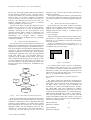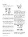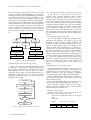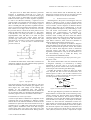
1
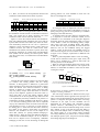
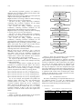
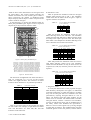
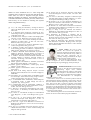
1468
JOURNAL OF COMPUTERS, VOL. 5, NO. 10, OCTOBER 2010
Extraction and Simulation of Intra-gate Defects
Affecting CMOS Libraries
Aymen Ladhar
STMicroelectronics, Ariana, Tunisia
Electronics, Micro-technology and Communication Laboratory, Sfax, Tunisia
Email: [email protected]
Mohamed Masmoudi
Electronics, Micro-technology and Communication Laboratory, Sfax, Tunisia
Email: [email protected]
Abstract—Shorts and opens are the most common type of
defects in digital integrated circuits ICs. They can affect
interconnect wires connecting gates or transistors inside.
Tools targeting the extraction of these potential defects focus
only on the inter-gate bridging faults, and no one presents a
solution to extract potential intra-grate bridging faults, open
and resistive-open defects. This paper presents an
automated approach to extract and simulate potential intragate defects in standard cell library, based on the use of
verification and simulation CAD tools. As application, we
used these fault signatures to diagnose different types of
intra-gate defects. Experimental results show the efficiency
of our approach to isolate injected defects on industrial
designs.
Index Terms— Intra-gate defects, extraction, simulation,
layout analysis, fault diagnosis.
I.
INTRODUCTION
Nowadays, the world has been revolutionized by the
rapid growth in the semi-conductor field. As the IC
technology process becomes more complex and
minimum feature size approaches nanometer range,
manufacturing quality and yield are becoming more
sensitive to physical defects, imperfection and process
variations. These defects are not affecting only the
interconnecting wires between gates but also transistors
inside. The simulation of intra-gate faults is a challenging
task. In fact, some of these defects can be sequence
dependant, which means the test result depends on the
ordering of the test patterns, even though the circuit is
fully combinational. These defects can be also timing
dependant, which means the test results change with the
test speed [1].
Intra-gate defects can be classified on four main
classes upon their electrical behavior when they are
simulated:
- The first category is bridging fault that results from
shorting two lines that must not be connected.
- The second category is source drain open or stuckopen fault [4] resulting from a complete break between
circuit nodes that should be connected [5], Stuck-open
faults can cause sequential behavior and thus require a
certain sequence of patterns in order to be detected. The
first pattern excites the defect while the second one
detects it. It has been shown in [1] that changing the test
© 2010 ACADEMY PUBLISHER
doi:10.4304/jcp.5.10.1468-1477
speed, voltage and temperature, do not improve the test
effectiveness. The stuck-open fault can be detected by
stuck-at fault patterns at nominal condition.
- The third category is gate open defect resulting in a
complete break in the transistor gate, the behavior of this
fault is depending on the state of neighbored lines and
parasitic capacitances and resistances [6].
- The last category of intra-gate defects is resistive-open
defect that is defined as an imperfect circuit connection
that can be modeled as a defective resistor between the
circuit nodes that should be connected. The behavior of
this fault depends usually on the test speed and the
parasitic resistance value causing this defect [1]. It has
been also shown that the optimal test voltage and test
temperature depend on the defect location and defect
material respectively.
The knowledge of layout topology is mandatory to
have realistic simulation results of intra-gate defects. In
fact, these defects are generally originated either by
neighbored lines causing bridging faults, or by defective
contacts causing open defects. In order, to precisely
simulate intra-gate defects, it is mandatory to extract from
the cell’s layout all the neighbored lines as well as all the
contact placements and transistors linked by each contact
[27]. Previous works on neighbored lines extraction [2]
[3] focused only on the extraction of neighbored metal
wire connecting standard cell gates. This information is
then used for bridging fault test pattern generation or for
a realistic bridging fault diagnosis. To our knowledge, no
works has been proposed for the extraction of intra-gate
defects especially, defects caused by defective contacts.
The knowledge of contact placements becomes
mandatory for precise simulation. For example, it may
happen that a single contact disconnects many transistors
in the same time causing multiple open defects.
In this paper, we present an efficient methodology to
extract all the potential intra-gate defects affecting
standard cell libraries. Then we use this information to
simulate these potential defects. Their fault signatures are
then recorded in a fault dictionary. As application we use
the created fault dictionary for an intra-gate diagnosis
procedure [7] [8]. Our diagnosis methodology delivers
more precise and realistic transistor level diagnosis
results than [18]-[24]. In fact, the name of the shorted
JOURNAL OF COMPUTERS, VOL. 5, NO. 10, OCTOBER 2010
lines in case of intra-gate bridging fault and the names of
the disconnecting transistors in case of contact open or
resistive-open defects are presented in diagnosis results.
Previous works are not able to diagnose open defects
when the defective contact disconnects more than one
transistor. The algorithm proposed in this work can
diagnose intra-gate defects in presence of multiple
exercising conditions per pattern [24].
The rest of the paper is organized as follow. Section 2
explains how we proceed to extract intra-gate defects.
Section 3 explains how we create an intra-gate fault
dictionary containing all the fault signatures of all
potential transistor defects caused by neighbored lines
and defective contacts. In section 4 we present our
methodology
for
intra-gate
defects
diagnosis.
Experimental results are included in section 5, and finally
conclusions are drawn.
II.
OUTLINE OF THE METHODOLOGY
An overview of the proposed method to construct the
fault dictionary containing all the potential intra-gate fault
signatures is presented in figure 1. This fault dictionary is
then used to diagnose intra-gate defects affecting standard
cell libraries. The proposed method starts from the layout
database to generate in the final step a fault dictionary
containing the signatures of the entire intra-gate defects
inside each library cell. Our algorithm begins by
extracting all the neighbored lines inside those gates.
Then, it determines the topology of nets inside it, in order
to extract potential open and resistive open defects. In
fact, these defects are generally affecting contacts, that
link poly-silicon layer to metal layer, and diffusion layer
to metal layer.
Layout
Database
Shorts and Open
Extraction
Transistor
netlist
Calibre
Potential Intra-gate
Defects List
Intra-gate Defect
Simulation
Eldo
Fault Dictionary
Figure 1. Overview of the method to create the fault dictionary
Once all the potential intra-gate defects are identified.
They are injected in the transistor netlist and a post layout
simulation is performed in order to determine their fault
signatures. In the simulation, we consider all the possible
input combinations and we take into account sequence
dependant defects. All the simulation results are then
collected in a fault dictionary. This fault dictionary is
created only one time and then can be used for the
© 2010 ACADEMY PUBLISHER
1469
diagnosis of any circuit having the same technology as
the library technology.
The extraction of transistor defects is performed using
the verification CAD tool Calibre [9] [10]. However, the
post layout simulation is performed using Eldo simulator
[11]
III.
EXTRACTION OF INTRAGATE DEFECTS
In this section, we focus on the extraction of potential
bridging and open defects in the transistor level. For this
purpose, each neighbored lines can be a potential
bridging fault and each contact is a potential open or
resistive open defect.
A. Layer defintion
Before explaining our method to extract potential intragate defects, we explain in the following the method to
define the (x, y) coordinates of each layer and transistor
in the cell’s layout.
A layer X is defined in the cell’s layout by its (x, y)
coordinates, and a transistor M is defined by the (x, y)
coordinates of its poly-silicon gate.
(x1, y3)
(x2, y2)
(x1, y1)
p16
x1 y1
x1 y3
x2 y1
x2 y2
x3 y2
x3 y3
p24
…
(x3, y3)
(x3, y2)
(x2, y1)
(1)
(2)
Figure 2. Layer definition
For example, figure 2 shows one layer composed by
two shapes p1 and p2. The first one (1) p 1 is represented
by 6 couples of coordinates, and the second one (2) p 2 is
defined by 4 couples. The same figure 2 represents on the
right side the way that the calibre query server presents
these (x, y) coordinates of the shape (1).
B. Coordinates determination of potential intra-gate
defects
The calibre SVRF rules enable the development of
Design Rule Checks DRC and Layout Versus Schematic
LVS checks. We are focusing on the following parts on
the DRC checks. Those are used to determine the
coordinates of contacts and neighbored lines. Actually,
the calibre DRC rules allow computing the distance
between each layout shape of the same layer (1) (2) and it
compares the calculated distance to a certain Design For
Manufacturing DFM distance fixed by the technology
rules. The calibre DRC checks can calculate also the
width of the different shapes like contacts in the layout
database (3), and to compare it to a certain DFM distance
fixed by the technology rules.
METAL_SPACING {
external M1i < DFM_M1
}
(1)
POLY_SPACING {
external POi < DFM_PO
}
(2)
1470
JOURNAL OF COMPUTERS, VOL. 5, NO. 10, OCTOBER 2010
Contact_SPACING {
internal COi < DFM_CO
}
(3)
The method used, to determine the (x, y) coordinates
of all contacts and all the neighbored shapes in each cell,
consists to modify the DRC rule file, where the DFM
values are replaced by new once.
Modified
Rule file
Layout
Database
DRC results
data
Figure 3. Calibre DRC
Figure 3 shows how we proceed to determine the
coordinates of contacts and the neighbored shapes using
Calibre DRC. In fact, it uses technology rules in the rule
file to identify, check devices and connectivity in the
layout database for any errors. In this process, DRC
generates an ASCII report and a DRC results database,
which are used to locate errors. As inputs calibre DRC
has the layout database of the studied cell and a modified
DRC rule file. The minimal distances between metals and
poly-silicon shapes are equal to a new distance DFM
fixed according the library technology. The minimum
contact width is also changed to a new DFM value. Using
a modified rule file we are able to collect at the end of
this step the coordinates of all the contacts and the
coordinates of all the neighbored shapes that can be metal
shapes or poly-silicon shapes.
D. Net names determination of the neighbored lines
from (x, y) coordinates
In the previous section, we explained the method to
extract the coordinates of potential intra-gate defects.
This information will be used next to identify the net
name of each potential intra-gate defect using calibre
query server. The calibre query server is a licensed
database server allows the examination of the contents of
the Standard Verification Database (SVDB) generated by
LVS/LVS-H [10]. The calibre query server allows having
the entire layers name in the (x, y) placements for metal
and poly-silicon layers. However, the tool is not able to
identify the net name corresponding to contacts‘s
coordinates.
Figure 3 shows how we proceed with the calibre query
server in order to obtain from (x, y) coordinates the net
names of layers in these locations. As inputs, we
introduce the coordinates of the neighbored shapes and
the SVDB directory. As results, we collect all the net
names of all the layers on each physical coordinates. The
neighbored layers belong to the same net name are
dropped from the list of neighbored lines.
© 2010 ACADEMY PUBLISHER
SVDB
Directory
Calibre Query
Net names
Calibre DRC
ASCII
report
(x, y)
coordinates
Figure 4. Net name extraction using Calibre query
E. Open and resistive open extraction
Contacts and vias are the main cause of open and
resistive open defects in CMOS ICs. At the transistor
level, we can only find contacts linking metal layer to
poly-silicon or linking metal to diffusion layer. These
connections are analyzed in the following to identify
contact open defect’s effects, i.e. transistors that are
disconnected when an open contact defect occurs.
Figure 5 shows how we proceed to extract the topology
of all the nets in the transistor netlist using the calibre
query server. As inputs, we introduce the entire names of
all the nets and transistors in the transistor netlist as the
SVDB directory. As result we collect the (x, y)
coordinates of all transistors, defined by the coordinates
of these poly-silicon gates, thus the (x, y) coordinates of
each layer constituting each net in the transistor netlist.
Here we can distinguish 4 connection types:
- Case (1): A diffusion connection n or p: in this case the
transistors are directly linked without contacts.
- Case (2): A metal-poly connection: in this case the two
layers are connected by contacts. Each poly-silicon layer
connects the gates of nMOS and pMOS transistor.
- Case (3): A metal-diff connection: in this case the
metal layer connects the diffusion layer by contacts.
- Case (4): A diff-metal-poly connection: in this case the
diffusion and metal layers are connected by contacts. The
metal and poly-silicon layers are also connected by
contacts. This kind of connection is used to connect the
drain of transistors with gates of other transistors.
Transistor
Netlist
SVDB
Directory
Calibre Query
Net topology
And Placements
Transistor
Placements
Figure 5. Net topology using Calibre query
The algorithm used to determine what transistors are
disconnected in the transistor netlist, where an open
defect caused by contacts occurs, is described in figure 6.
From the net’s topology we distinguish the type of
connection. Here we focus on case (2), (3) and (4) since
JOURNAL OF COMPUTERS, VOL. 5, NO. 10, OCTOBER 2010
these connections contain contacts. Each one of these
connection contains either Metal-diffusion or Polysilicondiffusion connection. For the Metal-diffusion connection
we determine the number and the coordinates of each
shape constituting the n and p diffusions. Then, we look
for transistors that are linked to each one of these shapes.
The transistors that are connecting to the same diffusion
shape are linked by the same contact. The same algorithm
is used for the Poly-Metal connection. Notice that if a
layer is connected to another layer by more then one
contact this net will not be analyzed. Since we suppose
that an open defect cannot affect more then one times a
net.
Net Topology and (x, y)
placements
Metal-diff
connection
Poly-Metal
connection
Diff-Metal-poly
connection
Distinguish disconnecting
diffusion layers
Distinguish disconnecting
Poly layers
For each diff layer determine
the name of transistor linking
For each Poly layer determine
the name of transistor linking
Each one of these transistors are
linked to this metal with contact
Each one of these transistors are
linked to this metal with contact
Figure 6. Contact extraction algorithm
F. Full intra-gate defect extraction algorithm
Figure 7 shows the full extraction algorithm. It begins
by selecting a gate from the analyzed standard cell
library. Then, it determines the coordinates of contacts
and neighbored lines in each gate. Once this step is
performed, the net name of each neighbored lines are
determined. After this step, the contact extraction
algorithm is launched. Finally, a list of all potential intragate defects is collected.
Select a Gate
Coordinates Determination of Contacts
and Neighbored Shapes
Net name determination of
Potential Bridging Faults
Contact Extraction Algorithm
More Gates
Potential intra-gate
Defects List
Figure 7. Full intra-gate defect extraction algorithm
© 2010 ACADEMY PUBLISHER
1471
IV.
MODELING AND SIMULATING INTRAGATE DEFECTS
In this section, we describe how we proceed to
simulate these potential intra-gate defects already
extracted in the previous section. For this, we use a
transistor netlist containing all the parasitic capacitances
and resistances that have been extracted from the gate’s
layout. The simulation is done for each gate by injecting
all potential intra-gate defects one a time. The simulation
is done at nominal voltage. We simulate all the possible
input combinations using the vpattern voltage source
from the eldo library. The fault dictionary is structured
like a truth table where the expected and the faulty value
are mentioned for each input value and for each defective
location.
A. New transistor netlist construction
Once all the neighbored lines and potential contact
placements are identified, we perform a post layout
simulation in order to collect their faulty signatures. The
simulation is done with Eldo simulator [11]. For this
purpose, a new transistor netlist is constructed. In this
transistor netlist, each neighbored nets are linked by a
resistance RBF of 1 GΩ, each transistor gate is linked to
theirs source and drain by a resistance of 1GΩ. Indeed, it
has been shown in [12] that the use of TiSi2 can cause
bridging faults between G-S and G-D. And finally, each
contact is replaced in the transistor netlist by a resistance
ROP of 1Ω. The simulation of the transistor netlist with
these new parameters gives the same results than the old
one. But in modifying the value of one resistance we
collect as response the signature of this fault on this
location.
B. Simulation of intra-gate bridging fault
Intra-gate bridging fault results from shorting two nets
or more inside a cell. To simulate a short between two
neighbored lines we suppose that they are linked by a
parasitic resistance of 1Ω. The simulation of different
intra-gate bridging faults in different cells shows that:
- Some intra-gate bridging faults have the same effects
than a stuck-at fault on one of the primary inputs or the
output of the target gate.
- Some intra-gate bridging faults have no effect on the
gate‘s primary output and the gate is kept faulty-free.
- Some intra-gate bridging faults drive the gate’s
primary output to the opposite value for some excitation
values and keep the rest faulty free.
C. Simulation of open defect
Intra-gate open defects can be classified in two
categories upon their location on the cell:
- Open source or drain also known as stuck-open
fault.
- Open gate.
TABLE I.
ZPrevious
0
1
TRUTH TABLE OF A NAND 2 GATE
A
1
1
B
0
0
CGood
1
1
CFaulty
0
1
1472
JOURNAL OF COMPUTERS, VOL. 5, NO. 10, OCTOBER 2010
The open source or drain defect assumes a particular
transistor is permanently turned off, as a result, for
example, of a failed transistor or connection break [1] [5]
[13]. Open source or drain faults can cause sequential
behavior and thus require a certain sequence of patterns
in order to be detected. Generally, a sequence of two
patterns needs to be applied. The first pattern excites the
fault and the second detects it. For example, figure 8
shows a NAND gate with open defect in pMOS transistor
source, no current can pass throw this transistor. The truth
table I shows correct logic results for the first row when
the previous value is 0 however the same pattern can not
detect the fault when the previous value is 1. The reality
is that the AB = 01 vector puts node C in a floating or
high-impedance state, and there is no outlet for rapid
discharge of its high logic voltage charge from the
previous logic state. This one was stored in the load
capacitance CL. As result, a correct value is read when the
previous value is 1 and the fault is detected when
previous value is 0.
Figure 8. S-D open fault
To simulate this fault all the value of ROP resistances are
replaced by 1GΩ one at a time and their faulty signatures
are then recorded for each location.
(a)
(b)
fault test, if these defects will be detected they will be
detected as stuck-at-0 for the slow-to-rise fault, and will
be detected as a stuck-at-1 for the slow-to-fall fault.
V.
INTRAGATE FAULT DIAGNOSIS
Fault diagnosis is the process of isolating the source of
failure in a defective circuit, so that a physical failure
analysis can be performed to physically examine the root
cause of failure. Precise diagnosis of different defects
affecting chips helps the IC manufacturers to fix the
process problems and improve the yield leading to a low
cost and shorter time-to-market. The existing logic
diagnosis tools [14][15][16][17] can determine, by
analyzing the failure’s responses, the most likely
locations inside a failing die from which the failures
originate. These tools allow also the diagnosis of some
inter-gate defects such bridging fault and interconnect
open defects. However, these tools have limitation to
diagnose defects affecting the transistor level.
In the following, we explain our method to diagnose
intra-gate defects using the fault dictionary that we have
already constructed in the previous section. The method
uses the stuck-at fault diagnosis results to determine
intra-gate suspect cells then an intra-gate diagnosis
algorithm is performed to verify if the real defect is on
the interconnecting wire or inside the library cell
associated with the identified location.
A. Localizing potential intra-gate defect from inter-grate
diagnosis results
The stuck-at fault model is the most used fault model
in diagnosis. Generally, it is followed by a ranking
mechanism to see how close it is to the real defect
behavior [16]. The use of these counts can be extended to
locate suspect cells with intra-gate defects [20].
Consider the example in figure 10, where two faults
were injected. The first one on the interconnect wire
between gates C2 and C1, the second at transistor level
inside gate C3. Table II represents the response of this
circuit in presence of these two faults.
A
Figure 9. Open gate fault
The second category intra-gate open defects is open gate
defect that disconnects one transistor gate (figure 9.a) or
more (figure 9.b). The voltage of the floating gate
depends on the neighbored lines and parasitic
capacitances. In the simulation all the ROP are deleted one
by one and the netlist are simulated with floating lines.
The faulty signature is then recorded for each location.
D. Simulation of resistive open defect
A resistive-open defect is defined as an imperfect circuit
connection that can be modeled as a defective resistor
between the circuit nodes that should be connected. In the
simulation we replace the value of the resistance ROP by a
resistance of 0.5, 1, 5 MΩ one at a time and we record the
faulty signature. Simulation results show that intra-gate
resistive-open faults will cause both slow-to-rise and
slow-to-fall faults on the affected node. During stuck-at
© 2010 ACADEMY PUBLISHER
st1
PO1
C2
C2/B
C3/Z
C1
C3
B
PO2
Figure 10. An intra-gate defect in presence of st fault
The inter-gate diagnosis procedure can determine two
disjoint defective locations that are not interacting on any
primary outputs [25]. The first defect can be modeled by
a stuck-at 1 fault. However, the second one cannot be
modeled by any inter-gate fault model. The simulation of
stuck-at faults (st-1 and st-0), on the output of the faulty
location C3, shows that the combination of these two
fault models can explain all the failures caused by this
defect. However, several simulation results don’t predict
the observed responses. For example, the simulation of a
st-0 on the output of C3 drives PO2 to 0 for the input
value (AB=10). However, the test’s output PO2 is equal
JOURNAL OF COMPUTERS, VOL. 5, NO. 10, OCTOBER 2010
to 1. Here, we observe the miss-prediction between the
simulation results and the observed test responses.
TABLE II.
0
1
2
3
A
B
0
0
1
1
0
1
0
1
TRUTH TABLE OF THE DEFECTIVE CIRCUIT
Tester outputs
PO1
PO2
1
1/0
1/0
1
1/0
0/1
1
1/0
Sim (C3/Z st-1)
PO1
PO2
1
1
1
1
Sim (C3/Z st-0)
PO1
PO2
1
0/1
1
1
1
1
1
1
1/0
0
1/0
1/0
Generally, when an intra-gate defect affects a circuit,
the simulation of stuck-at fault or combination of stuck-at
fault, will explain all its faulty responses, but some
simulation results will not match the tester fails.
Figure 11 shows the relation between the SimulationFails (SF) obtained while simulating the circuit with an
injected fault and the Tester-Fails (TF) from the tester.
The relationship between the two sets is captured as
diagnostic counts. The failing observe points which are
common between TFs and are called Tester FailsSimulation Fails (TFSF). The observe points, which only
fail during simulation are called Tester Pass-Simulation
Fails (TPSF). On the contrary, the observe points, which
only fail on the tester, are called Tester Fails-Simulation
Pass (TFSP).
TF
TFSP
TFSF
SF
TPSF
Figure 11. Relation between TF and SF
TF: {0/PO2, 1/PO1, 1/PO2, 2/PO1, 3/PO2}
SFst1 (C3/Z): {1/PO2}
SFst0 (C3/Z): {0/PO2, 2/PO2, 3/PO2}
(1)
(2)
(3)
Consider the same sample in figure 10. The tester fails
(1) contains four failing patterns and five failing
elements. A failing pattern is defined as a pattern that
detects the failures associated with all the primary outputs
where the failures were observed. However, a failing
element is defined as a failing pattern associated with
only one primary output where the failure is observed.
The per turn diagnosis applied on this tester fails (1)
shows that three of the four failing patterns which
constitute this TF are SLAT patterns [26]. Patterns 0 and
3 are explained by the faulty candidate C3/Z, pattern 2 is
explained by the faulty candidate C2/B. However, pattern
1 is a Non SLAT failing patterns that can be explained
only by the combination of the two faults C3/Z and C2/B.
The simulation of a st-1 (2) and st-0 (3) on the output of
the failing gate C3 shows that the three fails caused by
this defect on the primary output PO2 are explained.
However, the simulation of st-0 on the output of C3
shows that {2/PO2} is a passing element belonging to
TPSF category. Table III shows the different diagnostic
counts for the considered example. As we can observe
there are two disjoint cones. Consequently, candidates
belonging to each one are not interacting for failing and
© 2010 ACADEMY PUBLISHER
1473
passing patterns. So, each candidate in each cone can
have its own diagnostic counts.
TABLE III.
Pin name
C3/Z
C3/Z
C2/B
DIAGNOSTIC COUNTS
model
St0
St1
St1
#TFSF
2
1
2
#TFSP
1
2
0
#TPSF
1
0
0
An intra-gate defect is diagnosed if all the extracted
excitation values on the inputs of the defective cell for its
failing and passing patterns are explained by a candidate
belonging to the fault dictionary.
To minimize the work space and save computing time,
it is important to select the minimum number of cell
candidates to be considered in the intra-gate diagnosis
algorithm. From the stuck-at diagnosis results, we assign
a new TFSFst01 counts for each failing primary output.
This count is the result of adding TFSFst1 and TFSFst0
counts. Once this step is performed, we select from each
defective cone all the candidates having the biggest
TFSFst01 counts. If more than one candidate exists, we
select those having the two lesser TPSF counts as shown
in figure 12. For example, experiments on different cells
show that:
- When a pattern-dependant defect exists the TPSFst01
counts will be minimum on the gate‘s input. Since, the
defect can be modeled by a stuck-at fault when the
previous pattern excites the defect.
- When an intra-gate bridging fault exists and no stuck
at fault on the inputs of the defective cell explains the
failures, we found that the TPSFst01 counts will be lesser
on the gate’s output.
TPSF = n0
TPSF = n1
TPSF = n2
n2 ≥ n1
n1 ≤ n0 in case of intra-gate bridging fault
n0 ≤ n1 in case of pattern-dependant defect
Figure 12. The TPSF counts
B. Determining excitation conditions from patterns with
multiple exercising conditions
The exercising conditions are defined as binary logic
value combinations that are applied on the input pins of a
library cell in the design during the capture phase of a test
pattern. To diagnose intra-gate defects these exercising
conditions on the input of each candidate cell are
determined for both failing and observable passing
patterns. However, determining the active excitation
conditions values from an industrial design is not a trivial
task. Indeed, it may occur that the intra-gate defect is
being exercised multiple times in different ways during
the capture phase of a test pattern causing multiple
exercising conditions [24]. This is due to various reasons
like multiple capture cycles, the presence of both leading
and trailing edge flops in the design etc.
1474
The following algorithm presents our method to
determine active excitation conditions from patterns with
multiple exercising conditions.
Step1: Collect the exercising conditions on the inputs and
outputs of each intra-gate candidate cell.
Step2: Divide the exercising conditions values belonging
to failing patterns into two sub-categories:
- The first one SECF (Single Exercising Conditions)
containing only excitation conditions for the failing
patterns with single exercising conditions.
- The second one MECF (Multiple Exercising
Conditions) containing excitation conditions for the
failing patterns with multiple exercising conditions.
Step3: Divide the exercising conditions values belonging
to passing patterns into two sub-categories:
- The first one SECP (Single Exercising Conditions)
containing only excitation conditions for the passing
patterns with single exercising conditions.
- The second one MECP (Multiple Exercising
Conditions) containing excitation conditions for the
passing patterns with multiple exercising conditions.
Step 4: Remove SECF from MECP and remove SECP from
MECF, then repeat step 2 and 3 until no SECF and no
SECP exist respectively in MECP and MECF.
Step 5: From the fault dictionary find the fault locations
matching all the SECF and all the SECP
Step 6: From the list obtained in step 5 find the
candidates that explain one of each MECP and one of
each MECF, then rank the candidates according the
number of excitation pattern used. The candidate that
explains these criteria with minimum input excitation
values is more likely to be the good candidate.
For sequence dependant defect, it is mandatory to
introduce the previous values in the multiple exercising
conditions algorithm.
Consider an example where a NAND gate has been
identified as a potential intra-gate defect. The stuck-at
fault simulation on the output of this gate shows that
patterns P1, P2 and P3 belong to category of failing
patterns, and patterns P4 and P5 are passing patterns.
Input excitation values for P1: {00} Æ failing pattern
Input excitation values for P2: {10, 11} Æ failing pattern
Input excitation values for P3: {10, 00} Æ failing pattern
Input excitation values for P4: {10, 00} Æ passing pattern
Input excitation values for P5: {10, 11} Æ passing pattern
So, for our example, the algorithm will produce the
following results: After step 2 and 3, the algorithm will
consider pattern P1 as SECF, so {00} is a failing
excitation condition. Pattern P2, P3 are considered as
MECF, P4 and P5 as MECP. In step 4 {10} is considered
as a passing excitation condition and {11} as a failing
excitation condition. In Step 5 and 6 we use the fault
dictionary to find the fault location that explains this
failure.
C. Diagnosis flow
Figure 13 shows the proposed flow of the proposed
intra-gate diagnosis algorithm for a failing die.
© 2010 ACADEMY PUBLISHER
JOURNAL OF COMPUTERS, VOL. 5, NO. 10, OCTOBER 2010
Select a failing pattern
Diagnose one failing
pattern
Collect the input excitation conditions
for the suspect candidates
More Failing
Patterns
Simulate all the suspect candidates
with all the test patterns
Compute the diagnostic counts
Collect the input passing conditions for
the suspect candidates
Select suspect candidates
Multiple exercising conditions
algorithm
Match the excitation input
conditions with fault
Diagnosis Results
Figure 13. Complete diagnosis flow
Figure 13 shows the proposed flow of the proposed
intra-gate diagnosis algorithm for a failing die.
The proposed method begins by selecting one failing
pattern from the tester data-log to diagnose it. The input
excitation conditions are then collected for each suspect
cell. Once all the failing patterns are diagnosed, the
suspect cells are simulated with all test patterns. After
this step, the diagnostic counts are computed. The input
exercising conditions for observable passing patterns are
determined. The multiple exercising conditions algorithm
is applied to find out the active excitation input values.
Finally, the fault dictionary is used to find out the intragate defect that matches the failures
VI.
EXPERIMENTAL RESULTS
The above methodology was implemented and run on
two different libraries to create two different fault
dictionaries. Then, we used these data to the intra-gate
diagnosis procedure already presented in this paper.
A. Extraction results
TABLE IV.
CHARACTERISTICS OF SOME STUDIED GATES
Gate name
HS65_LHS_XNOR2X3
HS658_LH_SDFPSQX18
HS65_LH_AO222X9
HS65_LH_MUX21X4
HS65_LH_2X2
HS65_LH_AOI222X18
HS65_LH_CB4IlX4
HS65_LH_NOR4ABX4
Transistor
counts
10
42
14
12
4
48
10
10
Neighbored
shapes counts
19-21
112-120
29-33
52-23
9-6
23-50
32-16
23-40
Contact
counts
14
46
21
22
9
60
16
15
JOURNAL OF COMPUTERS, VOL. 5, NO. 10, OCTOBER 2010
Table IV shows some characteristics of some gates from
ST 65nm library. The second column represents the
number of transistors for each of these gates. Column 3
shows respectively the number of neighbored metal
shapes and poly-silicon shapes. Column 4 represents the
contact counts for each gate.
In the following, we present the detailed results for
HS65_LHS_XNOR2X3 gate. Figure 14 and 15 represent
respectively its layout and its transistor netlist.
1475
B. Simulation results
Table VI presents the simulation results for intra-gate
bridging fault between lines 2 and 7. The simulation
results show that the defect drives the gate’s output to
opposite value for two patterns.
TABLE VI.
A
0
0
1
1
Vdd
B
A
Z
FAULTY HS65_LHS_XNOR2X3
(CASE OF BRIDGE)
B
0
1
0
1
ZGood
1
0
0
1
ZFaulty
1
1
1
0
Table VII presents the simulation results for open
defect affecting contact CO1 and CO13. The simulation
results show that this defect has a different output results
according to the output’s previous value. The stuck-open
fault model is not adequate for the defect affecting CO13
since it disconnects more than one transistor.
2
TABLE VII.
7
Gnd
8
9
Figure 14. HS65_LHS_XNOR2X3 layout
M0 vdd A 2 17 PHVTLP L=0.06 W=0.28 $X=390 $Y=1310 $D=56
M1 vdd B 2 17 PHVTLP L=0.06 W=0.28 $X=430 $Y=2100 $D=56
M2 Z 2 vdd 17 PHVTLP L=0.06 W=0.55 $X=735 $Y=1310 $D=56
M3 9 B Z 17 PHVTLP L=0.06 W=0.55 $X=1035 $Y=1310 $D=56
M4 vdd A 9 17 PHVTLP L=0.06 W=0.55 $X=1225 $Y=1310 $D=56
M5 8 B 2 18 NHVTLP L=0.06 W=0.2 $X=250 $Y=525 $D=39
M6 gnd A 8 18 NHVTLP L=0.06 W=0.2 $X=460 $Y=525 $D=39
M7 7 2 gnd 18 NHVTLP L=0.06 W=0.39 $X=770 $Y=525 $D=39
M8 Z B 7 18 NHVTLP L=0.06 W=0.39 $X=1035 $Y=525 $D=39
M9 7 A Z 18 NHVTLP L=0.06 W=0.39 $X=1305 $Y=525 $D=39
Figure 15. transistor netlist
The extraction of neighbored lines shows that lines 2Gnd, 2-A, 2-Vdd, Gnd-7, 2-7, 2-Z, 7-Z, A-Z, B-A, B-Vdd,
and B-2 are neighbored lines. The extraction of contact
locations shows that there are 14 potential open defects.
TABLE V.
CONTACT LOCATIONS
Contact name
Net name
transistors
CO1
CO2
CO3
CO4
CO5
CO6
CO7
CO8
CO9
CO10
CO11
CO12
CO13
CO14
Vdd
Vdd
2
B
2
Z
A
2
A
Z
7
7
Gnd
2
M4
M0 M1 M2
M1
M M3 M5 M8
M0
M2 M3
M0 M6
M2 M7
M4 M9
M8 M9
M9
M7 M8
M6 M7
M5
Table V gives the location of the potential open defect
for each contact. For example, an open defect on contact
CO2 will disconnect Vdd from M0, M1 and M2
transistors in the same time.
© 2010 ACADEMY PUBLISHER
ZPrevious
1
1
1
1
0
0
0
0
FAULTY HS65_LHS_XNOR2X3
(CASE OF OPEN DEFECT)
A
0
0
1
1
0
0
1
1
B
0
1
0
1
0
1
0
1
ZGood
1
0
0
1
1
0
0
1
ZCO13
1
1
1
1
1
1
1
1
ZCO1
1
0
0
1
0
0
0
1
Table VIII presents the simulation results for resistive
open defect affecting contact CO13. The simulation
results show that the defect can only be observed for the
sequences (01) and (10) when the previous value of Z is
equal to 1.
TABLE VIII. FAULTY HS65_LHS_XNOR2X3
(CASE OF RESISTIVE-OPEN DEFECT)
ZPrevious
1
1
1
1
0
0
0
0
A
0
0
1
1
0
0
1
1
B
0
1
0
1
0
1
0
1
ZGood
1
0
0
1
1
0
0
1
ZCO13
1
1
1
1
1
0
0
1
C. Diagnosis results
To verify the effectiveness of the proposed intra-gate
fault dictionary developed in this paper, we elaborated
controlled experiments in which the behavior of failing
chip with an intra-gate fault was simulated. This was
performed by injecting intra-gate defects in a list of
library cell instances then their fault signature for the
whole circuit is recorded.. The method used to simulate
intra-gate defects, without a transistor level simulator,
consists of replacing the target cells by modified ones in
the library netlist. This modified cell represented a
defective version of the original cell, by having changed
its truth table or behavior. The modified netlist was then
simulated against stuck-at test patterns, and the failures
1476
JOURNAL OF COMPUTERS, VOL. 5, NO. 10, OCTOBER 2010
were recorded in data-log. These data-logs are then used
in the diagnosis step.
TABLE IX.
Circuit
A
B
Gate count
40
382224
CIRCUITS STATISTICS
Gate type count
15
777
Pattern #
14
3131
Scan chains #
1
8
Table IX shows some characteristics of the two circuits
used to verify our intra-gate diagnosis approach. The
circuit A is a sample circuit with only 40 gates. The
circuit B is in production at STMicroelectronics. The
second column presents the number of gates in each
circuit. The third column shows the number of gate type
counts in each circuit. This number is very small
comparing to the gate counts which means that the use of
fault dictionary is practical since each gate in the circuit
is used many times.
1) Experiment results for intra-gate bridging faults
diagnosis
Table X shows the results for conventional stuck-at
diagnosis for 6 intra-gate bridging faults injected in
different sample of circuit B. Column 1 shows the suspect
intra-gate cells, column 2 represents the number of failing
elements on each data-log. Column 3 to 6 indicate the
stuck at diagnostic counts on each candidate cell‘s output.
TABLE X.
Gate name
TF
F_AN2LLP
AO4ALL
F_MUX21NLL
F_ND4LL
OR5HS
AO7LL
2267
854
1265
237
331
524
STUCK-AT FAULTS DIAGNOSIS
Stuck-at fault diagnosis
TFSFst0
TFSFst1
TPSFst0
1948
125
0
205
268
295
319
729
1265
32
63
229
0
500
0
56
524
1176
TPSFst1
713
0
68
159
649
367
Table XI shows the intra-gate diagnosis results
obtained by our diagnosis flow on each suspect cell in
table X. Column 2 presents the number of suspect
transistors on each candidate cell. Columns 3 to 6 show
respectively the SECF, MECF, SECP and MECP counts
that are used in the multiple exercising conditions
algorithm. Column 7 shows the intra-gate bridging fault
candidate matching the defect behavior. For example, the
cell candidate F_AN2LLP has 6 transistors. A stuck-at
fault on its output explains 86 failing patterns and cause
36 passing patterns. The extraction of exercising
conditions on the inputs of this cell shows that 16 of the
failing patterns are SECF, however 70 are MECF. In the
same way, 24 of the passing pattern cause SECP, however
12 are MECP. Using the fault dictionary, we found a
bridging fault between the gate and drain of transistor M0
explaining this failure.
TABLE XI.
INTRA-GATE BRIDGING FAULT DIAGNOSIS
Gate name
Trans
SECF
MECF
SECP
MECP
Defect
F_AN2LLP
AO4ALL
F_MUX21NLL
F_ND4LL
OR5HS
AO7LL
6
10
12
8
14
6
16
29
23
12
22
36
70
7
52
4
105
85
24
3
6
25
12
29
12
2
23
9
23
8
Br G-D M0
Br 2-7
Br 5-2
Br G-D M5
Br 9-12
Br G-D M5
© 2010 ACADEMY PUBLISHER
2) Experiment results for intra-gate Open defect
diagnosis
Table XII shows the corresponding diagnosis results
for transistor stuck-open faults. For circuit A, three stuckopen defects were injected on contacts linking a net to
many transistors. Unlike bridging fault, excitation of
transistor stuck-open fault depends on previous values.
Therefore, exercising conditions were collected for
previous and current vectors. In all cases, we obtained the
good intra-gate candidate that explains the failures. For
example, the AO22X4 cell has been identified as
suspected cell for intra-gate defect. In fact, all the TF are
explained and some TPSF counts exist. This cell contains
10 transistors and 17 contacts. We were able to identify
the defective contact using our diagnosis approach.
TABLE XII.
INTRA-GATE DIAGNOSIS RESULTS FOR OPEN DEFECT
Gate name
Trans.
XOR2X4
AO1FX2
AO22X4
Stuck-at diagnosis results
Defect
TFSF
TFSP
TPSF
10
8
4
5
0
0
1
3
CO2
CO5
10
9
0
2
CO4
Figure 16 represents the layout of the gate AO22X4
that has been diagnosed as defective previously. This gate
is from the STMicroelectronics 65nm library. The
defective contact CO4 disconnects M1, M3 transistors
from M2 and M4 transistors, causing multiple stuck-open
defects. Our method was able to diagnose this defect
since it is based on the use of physical information
whereas other published works fails to identify the
correct faulty location.
Defective Contact
Figure 16. AO22X4’s layout
3) Experiment results for intra-gate resistive open
defect diagnosis
Table XIII shows the corresponding diagnosis results
for a NAND2X4 gate with a resistive open defect. The
value of the injected resistive open defect is 5 MΩ.
Columns 3 to 5 show the stuck-at diagnosis counts, and
column 6 shows the defective contact explaining the
failures.
TABLE XIII.
INTRA-GATE DIAGNOSIS RESULTS FOR RESISTIVE OPEN
Gate name
Trans.
NAND2X4
4
Stuck-at diagnosis results
TFSFst01
TFSP st01
TPSF st01
4
0
3
VII.
Defect
CO1
CONCLSION
In this paper, we have presented a method to automate
the extraction and the simulation of intra-gate defects
affecting standard cell library. The proposed method uses
the verification CAD tools calibre and SVRF rule file to
extract potential intra-gate defect. All the extracted
JOURNAL OF COMPUTERS, VOL. 5, NO. 10, OCTOBER 2010
defects are then simulated one at a time using Eldo
simulator then recorded in an intra-gate fault dictionary.
These data are used to diagnose intra-gate defects
affecting standard cell libraries. Experimental results in
controlled simulated environment prove the effectiveness
and accuracy of our method in isolating the injected
defect using fault dictionary.
REFERENCES
[1] J. Li, C.W. Tsang E.J. McCluskey “Testing for Resistive
Opens and Stuck Opens” Proc, Int Test Conf 2001 pp
1049-1058.
[2] S. T. Zachariah and S Chakravarty “Extraction of TwoNode Bridges From Large Industrial Circuits” IEEE Trans
CAD 2004 pp 433- 439.
[3] D. Walker and Z. Stanojevic “FedEx: Fast-bridging fault
extractor,” in Proc. IEEE Test Conf., 2001 pp. 696-703.
[4] C. Di and J. Jess, “On accurate modeling and efficient
simulation of CMOS opens,” in Proc. Int. Test Conf.,
Baltimore, MD, 1993 pp. 857–882.
[5] J. Li et al, “Diagnosis for Sequence Dependent Chips”,
VLSI Test Symposium, 2002, pp.187-192.
[6] V. Champac, A. Rubio, and J. Figueras, “Electrical Model
of the floating gate defect in CMOS IC’s: Implications on
IDDQ Testing” IEEE Trans on CAD 94 pp 359-356.
[7] A. Ladhar, L. Bouzaida, and M. Masmoudi “Layout Based
Method to Diagnose Intra-gate Defects in Presence of
Multiple-Fault” in Proc of IEEE SCS conference, 2008
[8] A. Ladhar, L. Bouzaida, and M. Masmoudi “Efficient and
Accurate Method to Diagnose Intra-gate Defects in
Nanometer Technology and Volume Data” in Proc of
DATE conference, 2009
[9] Mentor graphics documentation, “Standard Verification
Rule Format (SVRF) Manual”, Calibre v2007.4
[10] Mentor graphics documentation “Calibre Query Server
Manual”, Calibre v2007.4
[11] Mentor graphics documentation “Eldo’s user Manual”
Eldo v2007.2
[12] HP. Kuan X.M. Zhang “Physical analysis of TiSi2
bridging (gate-to-S/D) failure in IC” Proc IPFA Singapore,
IEEE 2005.
[13] S.M. Menon, et al “Testable Design of BiCMOS Circuits
for Stuck-Open Fault Detection using Single Patterns”
VLSI Test Symposium, April 1993. pp. 296-302.
[14] J. A. Waicukauski and E. Lindblooom, “Failure Diagnosis
of Structured VLSI”, in IEEE Design and Test of
Computers, Aug. 1989, pp 49-60.
[15] S. Venkataraman and S. B. Drummonds, “POIROT: A
Logic Fault Diagnosis Tool and Its Applications”, in Proc.
of Inter. Test conf. 2000, pp 253-262.
[16] C. Hora et al, “On Electrical Fault Diagnosis tool in fullscan circuits”, in Workshop on Defect Based Testing,
2001, pp 17-22.
[17] W. Zou et al, “On Methods to Improve Location Based
Logic Diagnosis “, in Proc. VLSI Design, 2006, pp 181187.
[18] X. Fan et al, “A Novel Stuck-at Based Method fot
Transistor Stuck-Open Fault Diagnosis”, in Proc. of
International Test Conference 2005, paper 16.1
[19] X. Fan et al, “A gate Level Method for Transistor-Level
Bridging Fault Diagnosis” in Proc. Of VLSI Test Symp.
2006, pp 266-271.
[20] X. Fan et al, “Extending Gate-Level Diagnosis Tools to
CMOS Intra-Gate Faults”, in Trans. In Silicon Debug and
Diagnosis 2007 pp 685-693
© 2010 ACADEMY PUBLISHER
1477
[21] E. Amyeen and al “Improving Precision Using Mixed
Level Fault Diagnosis” in Proc. of Inter. Test conf. 2006
paper 22.3
[22] J. Li and E. J. McCluskey “Diagnosis of Resistive-Open
and Stuck-Open Defects in Digital CMOS ICs” in Trans.
On Computer aided Design, 2005 pp 1748-1759.
[23] R. Desineni et al “A Logic Diagnosis Methodology for
Improved localization and Extraction of Accurate defect
Behavior” in Proc. of Inter. Test conf. 2006.
[24] M. Sharma et al, “Faster Defect localization in Nanometer
Technology based on Defective Cell Diagnosis” in Proc. of
Inter. Test conf. 2007 paper 15.3
[25] [12] Z. Wang et al “An Efficient and Effective
Methodology on the Multiple Fault Diagnosis” in Proc. of
Inter. Test conf. 2003 pp. 329-338
[26] T. Bartenstein, D. Heaberlin, L. Huisman, and D.
Sliwinski, “Diagnosing combinational logic design using
the single location at-a-time (slat) paradigm,” in in Proc. of
Inter. Test conf. 2001, pp. 287–296.
[27] A. Ladhar, M. Masmoudi, and L. Bouzaida “Extraction
and Simulation of Potential Bridging Faults and Open
Defects Affecting Standard Cell Libraries” in Proc of IEEE
SCS conference, 2008
Aymen Ladhar was born in Sfax,
Tunisia. He received the diploma in
Electrical engineering and M.Sc. degrees in
Electronics from the University of Sfax, in
2006 and 2007, respectively. He is
currently working toward the Ph. D. degree
at the University of Sfax, Tunisia.
His research works during B.Sc. M.Sc.
and Ph. D degrees are done in STMicroelectronics. They
include fault diagnosis, logic debugging, and layout analysis.
Mohamed Masmoudi was born in Sfax,
Tunisia, in 1961. He received the Electrical
engineering
degree
from
National
Engineering School of Sfax in 1985 and the
Ph. D degree in microelectronics from the
Laboratory of Computer Sciences, Robotics
and Microelectronics of Montpellier,
Montpellier, France in 1989.
From 1989 to 1994, he was an Associate professor with the
National Engineers School of Monastir, Tunisia. Since 1995, he
has been with the National Engineering School of Sfax, where,
since 1999, he has been a Professor engaged in developing
microelectronics in the engineering program of the university,
and where is also the head of the Laboratory Electronics, Microtechnology and Communication. He is the author and coauthor
of several papers in the microelectronics field. He has been a
reviewer for several journals.
Prof. Masmoudi organized several international conferences,
and has served on several technical program committees.