1
Graphics Master
User’s Manual
ADS document # 110110-9001B
Applied Data Systems
www.applieddata.net
9140 Guilford Road
Columbia MD 21046
301-490-4007
© 2001 ADS
Graphics Master User’s Manual
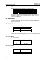
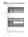
Revision History
ADS document # 110110-9001B.
REV
A
B
DESCRIPTION
Initial release
Clarify USB settings, descriptions and usage
(sections 3.6.13 and 3.6.14)
Add information about ADSmartIO power
(section 3.6.15)
Add note about IrDA control (3.7.7)
Clarify and add details about backlight control
signals (section 3.7.13)
Add power consumption measurements (4.5)
Expand and clarify Power Management
description (section 4.6)
Correct A/D input voltage range, ADSmartIO
(section 4.8.1)
Edit for improved readability
DATE
4/25/01
BY
ak
10/08/01
ak
About the Cover Photo
The cover photo shows a fully populated Rev A Graphics Master with 16MB of onboard flash.
ADS document # 110110-9001B
Page i
Graphics Master User’s Manual
(This page intentionally blank)
Page ii
ADS document # 110110-9001B
Graphics Master User’s Manual
Table of Contents
Revision History.................................................................................................................................................... i
About the Cover Photo .......................................................................................................................................... i
Table of Contents ................................................................................................................................................ iii
1
Introduction ...................................................................................................................................... 7
1.1
Overview ................................................................................................................................ 7
1.2
What’s New for the Graphics Master?.................................................................................... 7
1.2.1
1.2.2
1.2.3
1.2.4
1.3
Features................................................................................................................................... 8
1.3.1
1.3.2
1.3.3
1.3.4
1.3.5
1.3.6
1.4
2
3
New Features ................................................................................................................ 7
Changes in Connectors ................................................................................................. 7
Form Factor .................................................................................................................. 7
Other Key Differences.................................................................................................. 8
Processor....................................................................................................................... 8
Memory ........................................................................................................................ 8
Communications........................................................................................................... 8
User Interface and Display ........................................................................................... 9
I/O................................................................................................................................. 9
Audio .......................................................................................................................... 10
Block Diagram...................................................................................................................... 10
Getting Started................................................................................................................................ 11
2.1
Evaluation Systems............................................................................................................... 11
2.2
Frequently Asked Questions................................................................................................. 11
2.3
Organization of this Manual ................................................................................................. 12
2.4
For Further Information... ..................................................................................................... 12
Hardware Reference ....................................................................................................................... 13
3.1
Locating "Pin 1" ................................................................................................................... 13
3.2
Switches................................................................................................................................ 13
3.2.1
3.2.2
3.3
SW1: Reset Switch .................................................................................................... 13
S1: DIP Switch .......................................................................................................... 13
Potentiometers ...................................................................................................................... 13
3.3.1
3.3.2
VR1: Contrast Adjustment ........................................................................................ 13
VR2: Passive Panel Voltage Adjustment................................................................... 13
3.4
ADSmartIOTM ....................................................................................................................... 13
3.5
Onboard LEDs...................................................................................................................... 14
ADS document # 110110-9001B
Page iii
Graphics Master User’s Manual
3.6
Jumper Settings..................................................................................................................... 14
3.6.1
3.6.2
3.6.3
3.6.4
3.6.5
3.6.6
3.6.7
3.6.8
3.6.9
3.6.10
3.6.11
3.6.12
3.6.13
3.6.14
3.6.15
3.6.16
3.6.17
3.7
Connector Pinouts................................................................................................................. 19
3.7.1
3.7.2
3.7.3
3.7.4
3.7.5
3.7.6
3.7.7
3.7.8
3.7.9
3.7.10
3.7.11
3.7.12
3.7.13
3.7.14
3.7.15
3.7.16
3.7.17
3.7.18
3.7.19
3.7.20
3.7.21
3.7.22
3.7.23
4
J1: Contact Closure Detect ........................................................................................ 19
J2: USB, A/D, Digital I/O.......................................................................................... 19
J3: Battery Connector ................................................................................................ 20
J4: Touch Panel ......................................................................................................... 20
J5: Power Input.......................................................................................................... 21
J6: PS/2 Trackpad/Keyboard Input............................................................................ 21
J7: Serial Ports 1 and 2, Matrix Keypad, Power Outputs .......................................... 21
J8: Ethernet................................................................................................................ 23
J9: Manufacturing Test.............................................................................................. 23
J10: Serial Port 3...................................................................................................... 23
J11: PCMCIA .......................................................................................................... 23
J12: Flat Panel (Hirose connector)........................................................................... 24
J13: Backlight Inverter ............................................................................................ 25
J14: Flat Panel (IDC 34) .......................................................................................... 25
J15: Manufacturing Test.......................................................................................... 26
J16: Speaker............................................................................................................. 26
J17: Microphone ...................................................................................................... 26
J18: CAN Bus.......................................................................................................... 27
J20: USB Master, Serial Ports A-D, Codec ............................................................. 27
J22: PS/2 Mouse ...................................................................................................... 28
J23: USB.................................................................................................................. 29
J24: Compact Flash ................................................................................................. 29
J25: Thermistor Input .............................................................................................. 29
System Integration.......................................................................................................................... 31
4.1
Tips for System Integration .................................................................................................. 31
4.1.1
4.1.2
4.2
Strategies for Backup Power ...................................................................................... 31
Electrical Tips............................................................................................................. 31
Mechanical Specifications .................................................................................................... 31
4.2.1
4.2.2
4.2.3
Page iv
JP1: Flat Panel Voltage Select................................................................................... 14
JP2: Panel RL ............................................................................................................ 14
JP3: Panel UD............................................................................................................ 14
JP5: Source of Sleep Mode Power............................................................................. 15
JP6: Onboard 3.3V Converter Select......................................................................... 15
JP7: Serial Port 2 Mode Select .................................................................................. 15
JP8 to JP11, JP14/15, JP25/26: Serial Port 1 Mode Select ........................................ 15
JP12: Flat Panel Vee (Contrast) Adjust Mode........................................................... 16
JP13: Flat Panel Data Voltage Select ........................................................................ 17
JP16: DCD-DTR loopback ...................................................................................... 17
JP17: DSR-DTR loopback........................................................................................ 17
J19: Flat Panel Vee Select ....................................................................................... 17
JP20/21: USB Hub Bypass/Tier Level Select.......................................................... 18
JP22/23: USB Internal Loopback ............................................................................ 18
JP24: ADSmartIOTM Power Source......................................................................... 18
JP25: Serial 1 Rx Receiver ...................................................................................... 18
JP26: Serial 1 Tx Source ......................................................................................... 19
Mechanical Drawing................................................................................................... 31
Mounting Holes .......................................................................................................... 32
Clearances................................................................................................................... 33
ADS document # 110110-9001B
Graphics Master User’s Manual
4.3
Input Power Requirements.................................................................................................... 33
4.3.1
4.3.2
4.3.3
4.3.4
4.3.5
4.3.6
4.3.7
4.3.8
4.4
Externally Available Voltages .............................................................................................. 34
4.5
Power Consumption.............................................................................................................. 35
4.6
Power Management .............................................................................................................. 35
4.6.1
4.6.2
Using Sleep Mode for Power Management ................................................................ 35
Sleep Mode and Power Failures ................................................................................. 35
4.7
EMI/RFI and ESD ................................................................................................................ 36
4.8
Electrical Specifications for I/O Ports .................................................................................. 36
4.8.1
4.8.2
4.8.3
4.8.4
5
+5.0V.......................................................................................................................... 33
+3.3V.......................................................................................................................... 33
VPERM ...................................................................................................................... 33
+12V (J5).................................................................................................................... 34
+/-12V (RS-232)......................................................................................................... 34
3.0V Battery Backup (J3) ........................................................................................... 34
“Power On” Output .................................................................................................... 34
EMI/RFI and Transient Suppression .......................................................................... 34
ADSmartIOTM Controller ........................................................................................... 36
UCB 1200................................................................................................................... 36
SA-1110...................................................................................................................... 37
LCD Panel .................................................................................................................. 37
Board Revision History .................................................................................................................. 39
5.1.1
5.1.2
Identifying the board revision..................................................................................... 39
Revision History ......................................................................................................... 39
ADS document # 110110-9001B
Page v
Graphics Master User’s Manual
(this page intentionally blank)
Page vi
ADS document # 110110-9001B
1
Introduction
1.1
Overview
The Graphics Master is a full-featured single board computer using the SA-1110 StrongARM
RISC microprocessor. The Graphics Master is designed to meet the needs of embedded and
graphical systems developers.
1.2
What’s New for the Graphics Master?
If you're familiar with the successful design of the Graphics Client Plus, you find that Graphics
Master shares many of the same core features. However, the Graphics Master adds significant
new functionality.
1.2.1 New Features
Compact flash socket
Onboard temperature sensing circuit
Support for advanced power management
StrongARM SA-1111 companion chip:
USB master
Support for external AC'97 codec
PS/2 mouse
Quad UART:
Ports A and B: Factory configured for 9-wire RS-232 or 3.3V CMOS
Ports B and C: 5-wire 3.3V CMOS
Supports J1708
Enhanced power management ("pulled plug protection")
1.2.2 Changes in Connectors
The following signals have changed on Graphics Master connectors. See the related connector
descriptions for details.
•
GPIOs 24 and 27 are no longer available on connector J7 (3.7.7)
•
The location of GPIO 25 on connector J7 has changed (3.7.7)
•
SA-1111 SSP signals are made available on pins 36 and 38 of J7 (3.7.7)
•
New connector J20 with quad UART, AC'97 codec signals and additional ADSmartIOTM
ports.
1.2.3 Form Factor
The Graphics Master is slightly larger than the Graphics Client Plus. Placement of the connectors
has also changed to better accommodate panel-mounting of the board. Consult the mechanical
drawings in section 4.2 for details.
ADS document # 110110-9001B
Page 7
Graphics Master User’s Manual
1.2.4 Other Key Differences
If you have developed an application on the Graphics Client Plus, here are additional important
differences you should know about the Graphics Master. Related sections in this manual are
referenced in parentheses.
1.3
•
Onboard LEDs 1 and 2 are now controlled by GPIO25 and 26, respectively. They can
also be controlled by off-board signals. (3.5)
•
The SA-1111 has assumed a number of the functions formerly controlled by other
systems on the Graphics Client Plus. These include:
PCMCIA and Compact Flash
Software control of Vee (3.6.8)
System controller
Backlight intensity (J13 pin 6)
•
ADSmartIO can continue to run when system is asleep1 (JP24, 3.6.15)
•
The backlight on/off signal (J13 pin 5) is driven by the system controller
Features
1.3.1 Processor
•
SA-1110 32-bit StrongARM
•
SA-1111 Companion Chip
•
Clock rates up to 206 MHz
•
16, 32 or 64 MB synchronous DRAM (1/2 of CPU clock)
•
8, 16 or 32 MB Flash
•
3.3 and 5V PCMCIA
1.3.2 Memory
1.3.3 Communications
1
Page 8
•
Ethernet, RJ45
•
CAN bus
•
USB Master with four-port hub; USB Client port
•
Seven Serial Ports
Serial 1: RS-232, RS-422, RS-485 or J1708
Serial 2: RS-232, 3.3V CMOS or IrDA
Serial 3: RS-232
Serial A and B: RS-232 or 3.3V CMOS
Serial C and D: 3.3V CMOS
With optional firmware. Contact technical support if needed.
ADS document # 110110-9001B
Graphics Master User’s Manual
1.3.4 User Interface and Display
•
Flat panel interface
•
Onboard Vee generator
•
Analog touch panel interface
•
PS/2 keyboard and mouse interfaces
•
ADSmartIOTM configurable for digital I/O, A/D inputs and keypad scanning
•
Four 10-bit analog inputs
•
Contact closure detection
•
Digital I/Os from processor
1.3.5 I/O
ADS document # 110110-9001B
Page 9
Graphics Master User’s Manual
1.3.6 Audio
1.4
•
Speaker output
•
Microphone input
•
Support for external AC97 codec
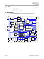
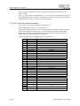
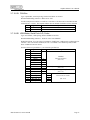
Block Diagram
The following diagram illustrates the system organization of the Graphics Master.
GRAPHICS MASTER
Power
Input
Primary
Regulator
5VDC
VDDI
Regulator
+3.3V
4 Wire Analog
Touch Screen
+1.75V
12V BL
Microphone 1
Interrupt
Controller
Software
Switches
(4)
Speaker 1
Secondary
Regulator
+3.3VCONT
Backup
Battery
Switch
Pushbutton
Reset
BOOT
ROM
128KB
SDRAM
16/32 Mbytes
SA1110
SSP
FLASH
8/16/32
Mbytes
RESET
High Density I/O Connectors
CODEC
UCB1200
Smart
Power
Management Configurable
IOs
AVR
Micrcontroller
SERIAL
Serial
Drivers
10 Digital IOs
4 Analog
Inputs
USB
SLAVE
8x8 Keypad Scan
8 Analog I/O
7 Digital I/O
External Interrupt
RS232/RS485/J1708
COM1
RS232/TTL
COM2
RS232
COM3
Quad
UART/Drivers
CAN BUS
INTERFACE
SA1111
PS2 Keyboard
PS2 Mouse
VEE
Generator
Panel
Drivers
USB
HUB
USB Master
USB Power
ETHERNET
5V/3V Panel Interface
Page 10
CAN BUS
Back
Light
Compact
Flash
PCMCIA
10BASE-T
IRDA
TX
RX
ADS document # 110110-9001B
Graphics Master User’s Manual
2 Getting Started
2.1
Evaluation Systems
Graphics Master boards are shipped as evaluation systems designed to get the developer up and
running quickly.
To use the system, simply plug power supply into the mini DIN-8 receptacle on the system.
If the screen does not display anything after five to ten seconds, check the Frequently Asked
Questions, below. Most operating systems cold boot within twenty seconds.
An evaluation system consists of the following:
•
Graphics Master single-board computer
•
Flat panel display and cable
•
Backlight inverter
•
Touch screen and cable
•
120VAC power supply
•
Plexiglas mounting
•
Developer's Cable Kit including
•
Serial Port 3 DB9 adapter (ADS cable #610110-4004A)
•
Serial Port 1 and 2 DB9 adapter (ADS cable #610110-4007A)
•
DB9F/F null modem cable
•
Operating system of your choice
•
User's Guide (this document and operating system guide)
•
Information about how to access ADS technical resources for the operating system you
have chosen.
Make sure you have received all the components before you begin your development.
2.2
Frequently Asked Questions
The following are some of the most commonly asked questions for evaluation systems:
Q: When I turn on power, my screen is white and nothing comes up on it.
A: Check the connector seating. The flat panel connector may have come loose in shipping.
Press it firmly into the panel and reapply power to your system.
Q: What does the pushbutton do?
A: The push button (SW1) issues a hard reset to the processor, which restarts the real-time clock
and may clear memory (RAM). Your application will most likely leave the system in sleep mode
when not in use, so this button will rarely be used by your customers. (ref. section 3.2.1)
Q: Do I have to turn off the system before I insert a PCMCIA or compact flash card?
A: Generally, no. The Graphics Master supports hot-swapping of PCMCIA and compact flash
cards. Consult the operating system documentation for details.
Q: Do I need to observe any ESD precautions when working with the system?
A: Yes. If possible, work on a grounded anti-static mat. At a minimum, touch an electrically
grounded object before handling the board or touching any components on the board.
ADS document # 110110-9001B
Page 11
Graphics Master User’s Manual
Q: What do I need to start developing my application for the system?
A: You will need a flash ATA card (8MB or larger) and the cables supplied with your system to
interface your development station to the system. For further direction, consult the ADS guide for
the installed operating system.
Q: Who can I call if I need help developing my application?
A: ADS provides technical support to get your development system running. For customers who
establish a business relationship with ADS, we provide support to develop applications and
drivers.
Q: Is there online support?
A: Yes. Information about the Graphics Master hardware (such as this manual) is available on the
ADS product page. ADS has operating-system-specific sites to support its customers. You should
have received information about ADS's developers' web site for the operating system you have
selected.
Q: Can I upgrade the version of the operating system?
A: Yes. ADS provides regular operating system updates on its developers' web site. For
operating systems not maintained by ADS, contact the operating system vendor.
Q: I would like to interface to a different display panel. How can I do this?
A: ADS may have already interfaced to the panel you are interested in. Consult ADS for
availability. ADS can interface to just about any panel you provide.
2.3
Organization of this Manual
The manual organizes information in three key sections:
Introduction
Provides an overview of the functionality and organization of the
Graphics Master.
Hardware Reference
Describes the configuration settings and connector pinouts for all
systems of the Graphics Master.
System Integration
Provides key information about power management, tips for system
integration and electrical and mechanical interface specifications.
To locate the information you need, try the following:
2.4
1.
Browse the Table of Contents. Section titles include connector designators and their
function.
2.
Follow cross-references between sections.
3.
View and search this manual in PDF format
For Further Information...
ADS maintains a web site exclusively for its developers. The site includes downloads,
troubleshooting guides, operating system updates and the "ADS Knowledge Base", a
comprehensive document with dozens of questions answered about developing applications for
ADS products. Instructions on how to access the site are shipped with every evaluation system.
Page 12
ADS document # 110110-9001B
3 Hardware Reference
This section gives an overview of the hardware features of the Graphics Master. This overview
includes a description of the switches, jumper settings, connector and connector pinouts.
3.1
Locating "Pin 1"
Many connectors and headers have a visible number on the board that indicates pin 1. If that pin
is not clearly marked, there are two other ways to locate pin 1:
1. The easiest method is to look at the underside of the board. The square pad is pin 1.
2. You can determine pin 1 from the mechanical drawing provided in section 4.2.
3.2
Switches
3.2.1 SW1: Reset Switch
SW1 is the reset switch for the Graphics Master. This switch issues a hardware reset to the SA1110. Press this button to restart the Graphics Master without cycling power. This operation will
reset the real-time clock. Most operating systems clear the contents of DRAM upon hardware
reset.
You can hold the Graphics Master in reset by pressing and holding this button.
3.2.2 S1: DIP Switch
S1 is a four-position DIP switch. It connects to the system/interrupt controller. The settings of
individual switches can be read from the controller. Some operating systems on the Graphics
Master reserve these switches for their use. Consult the operating system manual for details.
3.3
Potentiometers
3.3.1 VR1: Contrast Adjustment
You can adjust Vee (panel contrast) with the single-turn potentiometer VR1 on boards that have
the Vee option installed. You may also control Vee through software with the ADSmartIO
controller. See J19, JP12 and your operating system reference for further details.
3.3.2 VR2: Passive Panel Voltage Adjustment
You can adjust the VCON voltage on J14 pin 33 with the single-turn potentiometer VR2 on
boards that have that option installed. This potentiometer may be replaced by fixed resistors or
not installed at all in some Graphics Master configurations.
3.4
ADSmartIOTM
ADSmartIOTM is a second RISC microcontroller on the Graphics Master. This device provides
additional I/O functionality for specialized tasks. Your application software can configure the
standard ADSmartIO firmware for a variety of functions, including digital I/O, A/D and keypad
scanning.
ADSmartIO ports are available on J2 and J7. Consult your operating system reference guide for
the Graphics Master for details on how to make use of the ADSmartIO functionality.
ADS document # 110110-9001B
Page 13
Graphics Master User’s Manual
3.5
Onboard LEDs
The Graphics Master has three onboard LEDs. They are mapped as follows:
Signal
LEDOUT0
LEDOUT1
LEDOUT2
GPIO line
20
25
26
Part Designator
D3
D2
D1
Color
Green
Amber
Red
Note that, because GPIO25 and 26 also run to connector J2, LEDs 1 and 2 can be driven by or
used to monitor an external 3.3V signal. If you do this, make sure to configure the SA-1110
port(s) as input to avoid contention.
3.6
Jumper Settings
Jumpers on the Graphics Master select a variety of operational options. All use 2mm shorting
blocks (shunts) to select settings. Make sure power is turned off to the Graphics Master when
changing the position of a shunt.
3.6.1 JP1: Flat Panel Voltage Select
This jumper selects the supply voltage for the flat panel. The voltage selected here is passed to the
PNL_PWR connection (pins 28 and 29) on J12.
Jumper setting
Voltage Selected
1-2
3.3 V
2-3
5.0 V
WARNING! Make sure you have selected the correct voltage before connecting the panel. Flat
panels are sensitive to--and are often irreparably damaged by--incorrect voltages.
3.6.2 JP2: Panel RL
Type: 2-post header, 2mm
On some active flat panel displays, this signal flips the displayed image right-to-left.
Jumper settings
Connect RL to…
1-2
Ground
none
PNL_PWR
3.6.3 JP3: Panel UD
Type: 2-post header, 2mm
On some active flat panel displays, this signal flips the displayed image bottom-to-top.
Page 14
Jumper setting
Connect UD to...
1-2
Ground
none
PNL_PWR
ADS document # 110110-9001B
Graphics Master User’s Manual
3.6.4 JP5: Source of Sleep Mode Power
Type: 3-post header, 2mm
This jumper selects the source of power to back up the Graphics Master when it is in sleep mode.
See J5 for further details.
Jumper setting
Power supplied by
1-2
VPERM
2-3
VCC (+5V_IN)
3.6.5 JP6: Onboard 3.3V Converter Select
Type: 3-post header, 2mm
This jumper selects between an external 3.3V supply (+3.3V_IN) and the onboard 3.3V supply
(+3.3VINT), if installed. The onboard supply is installed as an option on the Graphics Master. J5
is the source of the external 3.3V supply.
Jumper setting
+3.3V connected to
1-2
+3.3V_IN (external)
2-3
+3.3VINT (internal)
3.6.6 JP7: Serial Port 2 Mode Select
Type: 2x12 header, 2mm
This header selects the communications mode of Serial Port 2 of the SA-1110. Odd-numbered
pins are on the side closer to the outer edge of the Graphics Master. Pins 1 and 2 are closest to
U7.
The operating system must configure the processor for the target serial mode. The table below
lists the standard voltages to expect on the transmit line of the port when the transmitter is idle.
Important: When using Serial 2 as IrDA, make sure that the operating system configures the port
as IrDA. Otherwise, the transmitter may be turned on continuously, which will drain significant
amounts of power and may damage IrDA transmitter.
Serial 2 Mode
RS-232
3.3V CMOS
IrDA
JP7 Shunt Settings
1-2, 3-4, 5-6, 7-8, 9-10,
15-16, 17-18, 23-24
1-3, 5-7
13-14, 21-22
11-12, 19-20
Tx Vidle
-6 V
3.3 V
0V
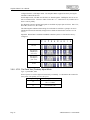
3.6.7 JP8 to JP11, JP14/15, JP25/26: Serial Port 1 Mode Select
Type: 3-post headers, 2mm
Jumpers JP8 through JP11 select between RS-232 and RS-485/422 mode and set the duplex mode
of RS-485/422/J1708.
RS-422, RS-485 and J1708 are differential serial protocols with the same voltage characteristics.
RS-422 is a point-to-point protocol while RS-485 and J1708 turn off the transmitter when not in
use, allowing multi-drop installations. J1708 enables the transmitter only when transmitting a "1"
while RS-485 powers the transmitter for high and low output. RS-485 and RS-422 can be
ADS document # 110110-9001B
Page 15
Graphics Master User’s Manual
configured in half- or full-duplex mode. The Graphics Master supports RS-422 by leaving the
transmitter enabled all the time.
In half-duplex mode, TX+/RX+ and TX-/RX- are shorted together. Half-duplex devices can see
their own transmissions. Connect to either of either the + or – connection on J7, but make sure to
observe correct polarity.
For diagnostic purposes, RS-485/422 signals are available on jumper pins as follows: JP8.1 TX+,
JP8.2 RX+, JP11.1 TX-, JP11.2 RX-.
The following table indicates shunt settings for each mode of Serial Port 1 (jumpers 24-26 are
included, but shown unconnected; settings for those shunts are described in sections 3.6.15 to
3.6.17).
JP15
J15
JP9
JP10
JP8
JP11
JP26
JP24
JP14
JP25
Important: RS-485/422 is installed on standard evaluation systems. J1708 must be factoryconfigured
RS-232
RS-485/422
Half Duplex
(two-wire)
RS-485/422
Full Duplex
(four-wire)
J1708
3.6.8 JP12: Flat Panel Vee (Contrast) Adjust Mode
Type: 3-post header, 2mm
Selects if panel Vee will be adjusted electronically or manually. Vee determines the contrast for
some panels. The polarity of Vee is set by J19.
Jumper setting
1-2
2-3
Page 16
Voltage Selected
Vee adjusted by PWM from
SA-1111 PWM1
Adjust voltage with
potentiometer VR1
ADS document # 110110-9001B
Graphics Master User’s Manual
3.6.9 JP13: Flat Panel Data Voltage Select
Type: 3-post header, 2mm
This jumper selects the voltage of the data lines for the flat panel display.
Important: These jumpers are set at the factory to match the panel and drivers shipped with the
system. They should not be changed by the user. You may damage the panel or panel drivers if
you change this jumper setting.
Tip: Most 5V panels will run correctly with 3.3V data.
Jumper setting
1-2
2-3
Voltage Selected
3.3 V
5.0 V
3.6.10 JP16: DCD-DTR loopback
Type: 2-post header, 2mm
This jumper loops the DTR signal of Serial Port 3 back out to DCD, which can simplify external
cabling for null modem connections. This jumper, along with JP17, can create a null modem
connection for some serial connections.
Jumper setting
1-2
Function
shorts pins 1(DCD)
and 7(DTR) of J10
3.6.11 JP17: DSR-DTR loopback
Type: 2-post header, 2mm
This jumper loops the DTR signal of Serial Port 3 back out to DSR. See notes for JP16.
Jumper setting
1-2
Function
shorts pins 2(DSR)
and 7(DTR) of J10
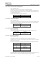
3.6.12 J19: Flat Panel Vee Select
Type: 6-post header, 2mm
This jumper selects both the source and polarity of the Vee voltage for the flat panel.
The control of Vee is set by JP12. You can adjust Vee either with VR1 (section 3.3) or through
software (JP12, section 3.6.8).
Note that Vee is installed only as an option and is not installed on all Graphics Master boards.
Jumper setting
Voltage Selected
none
none
2-4
Positive Vee
4-6
Negative Vee
3-4
+12V from J5.4
others
none
WARNING! Make sure you have selected the correct voltage before connecting the panel. Flat
panels are sensitive to--and are often irreparably damaged by--incorrect voltages.
ADS document # 110110-9001B
Page 17
Graphics Master User’s Manual
3.6.13 JP20/21: USB Hub Bypass/Tier Level Select
Type: 3-post headers, 2mm
These shunts select whether the SA-1111 or an external, upstream hub control the onboard USB
hub. The Graphics Master can act as the root (highest-level, Tier 0) node in the USB network or
can connect below another USB hub (in this case, the SA-1111 is disconnected from the USB
network). Setting the shunts to position 2-3 directly connects the SA-1111 master signal to USB
Hub 4 lines for systems that do not have the USB hub installed.
Important: Both shunts must be set to the same position.
Jumper setting
1-2
n/c
2-3
System acts as USB...
...Tier 0 (root node) connection
...Tier 1 connection
...single-port master on Hub 4
3.6.14 JP22/23: USB Internal Loopback
Type: 3-post headers, 2mm
These shunts connect the SA-1110 USB Slave port to Hub Downstream Port 1, creating an
onboard USB loopback. If this loopback is used, do not use the connections on J20 or J23. The
SA-1110 USB Slave port is always available on header J2.
Important: Both shunts must be set to the same position.
Jumper setting
n/c
1-2
USB Hub Port 1...
...is only connected to J20 &J23
...also loops back to
SA-1110 USB Slave
3.6.15 JP24: ADSmartIOTM Power Source
Type: 3-post header, 2mm
This jumper selects the power supply for the ADSmartIO. You may turn off ADSmartIO to
conserve power in sleep mode, or leave it on to continue performing base I/O functions or to assist
with power management. Note that your system may require special firmware to support this
feature.
Important: If ADSmartIO is turned off when in sleep mode, all its outputs will be off.
Jumper setting
1-2
2-3
In Sleep mode, ADSmartIO is...
OFF
ON
3.6.16 JP25: Serial 1 Rx Receiver
Type: 3-post header, 2mm
This jumper selects what device on the Graphics Master will receive data from the Serial 1 receive
input (J7 pin 12).
Jumper setting
1-2
2-3
Page 18
Serial 1 Rx Source
StrongARM CPU
ADSmartIO
ADS document # 110110-9001B
Graphics Master User’s Manual
3.6.17 JP26: Serial 1 Tx Source
Type: 3-post header, 2mm
This jumper selects what device on the Graphics Master supplies data to the Serial 1 transmit
output (J7 pin 14).
Jumper setting
1-2
2-3
3.7
Serial 1 Tx Source
StrongARM CPU
ADSmartIO
Connector Pinouts
The following tables describe connector pinouts and the type of connector. At least one pin of
every connector is labeled on the Graphics Master. Double-row headers on
2 4 6 8...
the board are all numbered as shown in the figure to the right.
1 3 5 7...
For information about the location of the connectors on the Graphics Master,
refer to section 4.2, Mechanical Specifications:
Legend:
n/c
GND
Not connected
Graphics Master ground plane
3.7.1 J1: Contact Closure Detect
Type: 2-pin header, 0.100-in spacing, friction lock, Molex 22-23-2021
Recommended mating connector: Molex 22-01-3027
External input. Short these pins together to generate a high level on GPIO1 of the SA-1110. Pin 2
can be used by the application or operating system for user input, contact closure detection or to
wake the system from sleep mode.
Pin
1
Signal name
GND
2
SWITCH
Description
Ground
to GPIO1 of SA-1110 via inverting buffer; includes
11kΩ pull-up to 3.3V and is powered. during Sleep
3.7.2 J2: USB, A/D, Digital I/O
Type: 2x15 header, 2 mm spacing, Samtec STMM-115-02-T-D
Recommended mating connector: TCSD-15 series from SAMTEC
Electrical specifications for signals are referenced in parentheses ( ).
Pin
1
3
5
7
9
ADS document # 110110-9001B
Signal name
UCB_IO0
UCB_IO1
UCB_IO2
UCB_IO3
UCB_IO4
UCB_IO9
UCB_IO8
UCB_IO7
UCB_IO6
UCB_IO5
Pin
Description
Digital I/Os (10)
2
4
6
8
10
(UCB1200, section 4.8.2)
Page 19
Graphics Master User’s Manual
Pin
11
13
15
17
19
21
23
25
27
29
Signal name
ANIN0
ANIN1
ANIN2
ANIN3
SMTIO0
SMTIO1
SMTIO2
SMTIO3
SMTIO4
SMTIO5
Pin
/EXT_IRQ
24
UCB_TINP
UCB_TINN
UCB_TOUTN
UCB_TOUTP
USB_VCC
USB_GND
USB_UDCUSB_UDC+
GND
Description
Analog inputs (4)
(UCB1200, section 4.8.2)
12
14
16
18
20
22
PB0
PB1
PB2
PB3
PD0
PD1
ADSmartIO lines (7)
(section 4.8.1)
External interrupt
3.3V CMOS with 10k pullup
Telecom interface
(UCB1200, section 4.8.2)
26
USB Slave
(SA-1100)
28
30
Ground
3.7.3 J3: Battery Connector
Type: 2-pin header, 0.100-in spacing, friction lock, Molex 22-23-2021
Recommended mating connector: Molex 22-01-3027
This connector allows you to connect an external battery to back up power on the Graphics
Master. If no other power source is available, the system will draw its sleep mode current (section
4.5) from this connection. There is a steady-state 1MΩ load across these terminals. For reliable
operation of the Graphics Master, place a 0.100" shunt across the pins of this connector.
Pin
1
2
Signal name
BATPOS
BATNEG
Description
3 Volt battery, positive terminal
Graphics Master ground
3.7.4 J4: Touch Panel
Type: 4-pin header, 0.100-in spacing, friction lock, Molex 22-23-2041
Recommended mating connector: Molex 22-01-3047
The mapping shown of signal to edge of touch panel is an ADS convention. Interface cables are
constructed to match this order. Some operating systems can tolerate swapping of positive (P) and
negative (M) connections, and even swapping of X and Y pairs.
Pin
1
2
3
4
Page 20
Signal name
TSMX
TSPX
TSPY
TPMY
Description
Left edge of panel
Right
Bottom
Top
ADS document # 110110-9001B
Graphics Master User’s Manual
3.7.5 J5: Power Input
Type: 6pin header, 0.100-in spacing, friction lock, Molex 22-23-2061
Recommended mating connector: Molex 22-01-3067
This connector supplies main and backup power to the Graphics Master. See section 4.3 for
additional details about input power requirements.
Pin
1
2
Signal name
+5V_IN
GND_IN
3
+3.3V_IN
4
+12V_IN
5
Power_Enable
6
VPerm
Description
main power: +5 Volts ±5%
Ground (filtered)
+3.3 Volts ± 5%
Required if onboard 3.3V supply option is not installed
To use, set JP6 to “external 3.3V.”
Optional 12V for PCMCIA (J11),
backlight (J13) and Vee (J19)
3.3V CMOS output; 0V when board power is disabled
see section 4.3.7 for further details
5-12V DC @5mA for sleep mode
3.7.6 J6: PS/2 Trackpad/Keyboard Input
Type: Mini DIN-6 socket housing, MDI-004-6PC
Recommended mating connector: PS/2 keyboard
Pin
1
2
3
4
5
6
Signal name
TPSIG
N/C
GND
VCC
TPCLK
N/C
Description
PS/2 trackpad/keyboard data
not connected
Ground
+ 5 Volts, fused at 350 mA
PS/2 trackpad/keyboard clock
not connected
3.7.7 J7: Serial Ports 1 and 2, Matrix Keypad, Power Outputs
Type: 2x20 header, 2 mm spacing
Recommended mating connector: TCSD-20 series from SAMTEC
Pin
1
3
5
7
9
11
13
15
ADS document # 110110-9001B
Signal name
ROW0
ROW1
ROW2
ROW3
ROW4
ROW5
ROW6
ROW7
RXD2
TXD2
CTS2
RTS2
GNDCOM2
Pin
Description
PC7
PC6
PC5
PC4
PC3
PC2
PC1
PC0
2
4
6
8
10
ADSmartIO
(see section 4.8.1)
Configurable as:
Digital I/O
Keypad, rows
SA-1110 Serial Port 2
RS-232 or CMOS (see JP7)
See also note below
Page 21
Graphics Master User’s Manual
Pin
Signal name
RXD1
TXD1
CTS1
RTS1
GNDCOM1
COL0
COL1
COL2
COL3
COL4
COL5
COL6
COL7
RX422+
RX422TX422+
TX422GNDRS422
GPIO25/LED1
GPIO26/LED2
17
19
21
23
25
27
29
31
33
VREF
35
37
39
VCC
+3.3V
GND
C7
C6
GND
Pin
12
14
16
18
20
Description
RS-232 Serial Port 1
from SA-1110 or ADSmartIO
(see section 3.6.7 for mode select,
JP25,26 for source select,
and note below about handshaking)
PA0
ADSmartIO
PA1
(see section 4.8.1)
PA2
PA3
Configurable as:
Analog Inputs
PA4
Digital I/O
PA5
Keypad, columns
PA6
PA7
22
24
26
28
30
32
34
RS-422/485 lines, Serial Port 1
(see section 3.6.7)
SA-1110 GPIOs
(see sections3.5 and 4.8.3)
Voltage reference for ADSmartIO A/D;
reference use only (<100µA)
+5V
+3.3V
Ground
36
38
40
SA-1111 GPIOs
Ground
Note: The SA-1110 does not have hardware handshaking on its serial lines. The Graphics Master
is wired to use SA-1110 GPIO lines to perform CTS/RTS handshaking as follows:
SA-1110
GPIO
14
15
16
17
18
19
Function
RS-232
CTS1
RTS1
CTS2
RTS2
CTS3
RTS3
RS-485
RX enable
TX enable
The IrDA transmitter is enabled with an active-low signal on GPIO23. The enable line has a pullup to disable the IrDA transmitter during initialization or when GPIO23 is an input.
Page 22
ADS document # 110110-9001B
Graphics Master User’s Manual
3.7.8 J8: Ethernet
Type: RJ-45 socket, Amp 555167-1
Recommended mating connector: RJ-45 plug.
Connects to the on-board Ethernet driver.
Pin
1
2
3
4
5
6
7
8
Signal name
ETHP1
ETHP2
ETHP3
Description
Transmit +
Transmit Receive +
n/c
ETHP6
Receive -
n/c
3.7.9 J9: Manufacturing Test
Type: 6-pin header, 1x6 0.100-inch spacing.
For manufacturing use.
3.7.10 J10: Serial Port 3
Type: 2x5 header, 0.100” IDC, keyed
Recommended mating connector: 2x5 IDC
Pin
Signal name
1
“DCD3”
2
“DSR3”
3
4
5
6
RXD3
RTS3
TXD3
CTS3
7
“DTR3”
8
9
10
n/c
GNDFILT3
n/c
Description
DCD from external device
see JP16 for loopback options
DSR from external device
see JP17 for loopback options
SA-1110 Serial Port 3, RS-232
DTR from external device
see JP16 and JP17 for loopback options
not connected
filtered connection to ground
not connected
Note: The SA-1110 does not have hardware handshaking on its serial lines. The Graphics Master
is wired to use SA-1110 GPIO lines to perform CTS/RTS handshaking. See the table on page 22
for port assignments.
3.7.11 J11: PCMCIA
Production option: Mating ejector Amp #146019-1
The 68-pin PCMCIA socket conforms to the PCMCIA standard for 3.3V and 5V Type II cards. It
will supply up to 500 mA of 5V current. The socket is normally de-energized; the operating
system is responsible for turning on the socket when a card is inserted and turning it off when the
card is removed.
ADS document # 110110-9001B
Page 23
Graphics Master User’s Manual
Ejector hardware is available for applications that require regular insertion and removal of
PCMCIA cards.
Note: VPP (pins 18 and 52) is supplied from the "+12V" input (pin 4 on J5). Since few PCMCIA
cards manufactured use this voltage, most applications can set the J5.4 input voltage to match the
backlight voltage needed. See section 4.3.4 for further details.
3.7.12 J12: Flat Panel (Hirose connector)
Type: Hirose 31-pin connector, 1mm pitch, #DF9B-31P-1V
Recommended mating connector: Hirose DF9B-31S-1V
This connector houses the signals to drive an 18-bit flat panel and will drive a Sharp LQ64D343
panel in StrongARM 16-bit mode directly. It can be found on the back side of the Graphics
Master. The only difference between this connector and J14 is that J12 does not include VEE.
Signals shown are for the StrongARM in 16-bit mode.
Electrical specifications for panel signals are listed in section 4.8.4.
Pin
1
2
3
4
5
6
7
8
9
10
11
12
13
14
15
16
17
18
19
20
21
22
23
24
25
26
27
28
29
30
31
Page 24
Signal name
PNL_GND
PNL_PIXCLK
PNL_HSYNC
PNL_VSYNC
PNL_GND
PNL_RED0
PNL_RED1
PNL_RED2
PNL_RED3
PNL_RED4
PNL_RED5
PNL_GND
PNL_GREEN0
PNL_GREEN1
PNL_GREEN2
PNL_GREEN3
PNL_GREEN4
PNL_GREEN5
PNL_GND
PNL_BLUE0
PNL_BLUE1
PNL_BLUE2
PNL_BLUE3
PNL_BLUE4
PNL_BLUE5
PNL_GND
PNL_LBIAS
Description
Panel ground
Pixel Clock
Horizontal Sync.
Vertical Sync.
Ground
Red Bit 0 (same as RED5)
Red Bit 1
Red Bit 2
Red Bit 3
Red Bit 4
Red Bit 5
Ground
Green Bit 0
Green Bit 1
Green Bit 2
Green Bit 3
Green Bit 4
Green Bit 5
Ground
Blue Bit 0 (same as BLUE5)
Blue Bit 1
Blue Bit 2
Blue Bit 3
Blue Bit 4
Blue Bit 5
Ground
Enable
PNL_PWR
Vcc(5V) or 3.3 V, depending on JP1 position
PNL_RL
PNL_UD
Horizontal Mode Select (set by JP2)
Vertical Mode Select (set by JP3)
ADS document # 110110-9001B
Graphics Master User’s Manual
3.7.13 J13: Backlight Inverter
Type: 7-pin header, 1.25mm, keyed, Molex #53261-0790
Recommended mating connector: Molex 51021-0700 or
Quadrangle Products kit #RT51021-0700-18
This connector will supply power to a Xentek LS520 backlight inverter and compatible devices
with a one-to-one cable. The onboard Graphics Master PWM driver can electronically control the
brightness of the inverter. Note that some of the control signals may not work with other
backlight inverters (see production options).
Production options:
5V pull-up for BACKLIGHTON signal
Power-up default for BACKLIGHTON is not GND
Pin
1
2
3
4
Signal name
5
BACKLIGHTON
6
BACKLIGHTPWM
7
GND
+12V
GND
Description
0-12 volts from J5.4
(see J5 and section 4.3.4)
Ground
Open-collector output + pullup to enable backlight
(shorted to GND for “off”) (system controller)
PWM brightness control (SA-1111)
(3.3V CMOS, 1.2kΩ series, 1µF filter)
Ground
3.7.14 J14: Flat Panel (IDC 34)
Type: 34-pin IDC header, 2x17 0.100-inch spacing, shrouded, keyed
Recommended mating connector: IDC connector AMP #1-746288-8
This connector houses the signals to drive an 18-bit flat panel. Electrical specifications for panel
signals are listed in section 4.8.4.
Pin
1
2
3
4
5
6
7
8
9
10
11
12
13
14
15
16
17
18
19
20
ADS document # 110110-9001B
Signal name
PNL_VEE
PNL_GND
PNL_PIXCLK
PNL_HSYNC
PNL_VSYNC
PNL_GND
PNL_RED0
PNL_RED1
PNL_RED2
PNL_RED3
PNL_RED4
PNL_RED5
PNL_GND
PNL_GREEN0
PNL_GREEN1
PNL_GREEN2
PNL_GREEN3
PNL_GREEN4
PNL_GREEN5
PNL_GND
Description
VEE (contrast); see VR1, J19 and JP12
Ground
Pixel Clock
Horizontal Sync.
Vertical Sync.
Ground
Red Bit 0 (same as RED5)
Red Bit 1
Red Bit 2
Red Bit 3
Red Bit 4
Red Bit 5
Ground
Green Bit 0
Green Bit 1
Green Bit 2
Green Bit 3
Green Bit 4
Green Bit 5
Ground
Page 25
Graphics Master User’s Manual
Pin
21
22
23
24
25
26
27
28
29
30
31
32
33
Signal name
PNL_BLUE0
PNL_BLUE1
PNL_BLUE2
PNL_BLUE3
PNL_BLUE4
PNL_BLUE5
PNL_GND
PNL_LBIAS
Description
Blue Bit 0 (same as BLUE5)
Blue Bit 1
Blue Bit 2
Blue Bit 3
Blue Bit 4
Blue Bit 5
Ground
Enable
PNL_PWR
Vcc(5V) or 3.3 V, depending on JP1 position
PNL_RL
PNL_UD
PNL_ENA
34
VCON
Horizontal Mode Select (set by JP2)
Vertical Mode Select (set by JP3)
Panel enable signal (StrongARM GPIO24)
Adjustable voltage for passive panels;
set with VR2 or fixed voltage divider
3.7.15 J15: Manufacturing Test
Type: 2x3 header, 0.100-inch spacing
For manufacturing use.
3.7.16 J16: Speaker
Type: 2-pin header, 0.100-in spacing, friction lock, Molex 22-23-2021
Recommended mating connector: Molex 22-01-3027
A speaker may be connected across the speaker outputs (bridge-tied load). Minimum speaker
impedance is eight ohms. Voltages on the speaker outputs are 0-3.3V. If you connect one side of
the speaker to ground, you must use a blocking capacitor; in this case, output power will be
reduced to one quarter and power consumption will be cut in half from that of the bridge-tied load.
Consult the UCB1200 specifications for further details.
Pin
1
2
Signal name
SPK SPK +
Description
Speaker connection (-)
Speaker connection (+)
3.7.17 J17: Microphone
Type: 2-pin header, 0.100-in spacing, friction lock, Molex 22-23-2021
Recommended mating connector: Molex 22-01-3027
Input impedance of the microphone connection is 25 kΩ. Specifications for the UCB1200 call for
1kΩ or electret microphones. Microphones with other impedance may be used. Microphones
connected should use a DC blocking capacitor between the microphone and MIC+ input.
Pin
1
2
Page 26
Signal name
MIC GND
MIC +
Description
Microphone (-)
Microphone (+)
ADS document # 110110-9001B
Graphics Master User’s Manual
3.7.18 J18: CAN Bus
Type: 2-pin header, 0.100-in spacing, friction lock, Molex 22-23-2021
Recommended mating connector: Molex 22-01-3027
Use this connection to connect to a CAN bus. Note that a CAN bus must be terminated at both
ends with 120Ω resistors. The Graphics Master does not include termination resistors onboard.
Pin
1
2
Signal name
CAN1HIGH
CAN1LOW
Description
CAN bus (+)
CAN bus (-)
3.7.19 J20: USB Master, Serial Ports A-D, Codec
Type: 2x25 header, 2 mm spacing, Samtec STMM-125-02-T-D
Recommended mating connector: TCSD-15 series from SAMTEC
Production options: For cost savings in production, UART ports A and B can be configured to use
external +/-12V (also on this connector) or to be 3.3V CMOS. On evaluation systems, UART
Ports A and B have RS-232 drivers.
Section references in parentheses ( ) are electrical specifications.
Pin
1
3
5
7
9
Signal name
HUB4+
HUB3+
HUB2+
HUB1+
HUB4HUB3HUB2HUB1HUBIN+
HUBIN-
11
USB VCC HUB
13
15
17
19
21
USB_GND+
DATA_OUT
DATA_IN
SYNC_OUT
BIT_CLK_IN
SYS_CLK
ADS document # 110110-9001B
Pin
Description
USB Hub
Downstream Ports
(SA-1111)
2
4
6
8
Upstream USB hub connection
(SA-1111)
USB power and ground (filtered)
(SA-1111)
10
12
C2
C3
C1
C0
External AC'97 Codec
(SA-1111)
Page 27
Graphics Master User’s Manual
Pin
23
25
27
29
31
33
35
37
39
41
43
45
47
49
Signal name
SMTIO6
SMTIO7
SMTIO8
SMTIO9
SMTIO10
TXDA
TXDA
CTSA
RTSA
DTRA
DCDA
DSRA
RIA
RXDB
TXDB
CTSB
RTSB
DTRB
DCDB
DSRB
RIB
GND_FILT
RXDC
TXDC
CTSC
RTSC
RXDD
TXDD
CTSD
RTSD
EXT+12V
EXT-12V
Pin
14
16
18
20
22
Description
PD2
PD3
PD4
PD5
PD6
ADSmartIO lines
(section 4.8.1)
Serial Port A
(RS-232 standard,
3.3V or ext. +/-12V optional)
24
26
28
30
32
34
36
38
40
Serial Port B
(RS-232 standard,
3.3V or ext. +/-12V optional)
Ground (filtered)
Serial Port C
(3.3V CMOS)
42
44
46
48
Serial Port D
(3.3V CMOS)
External +/-12V power input
for UARTs A & B (optional)
50
3.7.20 J22: PS/2 Mouse
Type: Mini DIN-6 socket housing, MDI-004-6PC
Recommended mating connector: PS/2 mouse, mini DIN-6
Pin
1
2
3
4
5
6
Page 28
Signal name
MSDATA
N/C
GND
VCC
MSCLK
N/C
Description
Mouse data
not connected
Ground
+ 5 Volts, fused at 350 mA
Mouse clock
not connected
ADS document # 110110-9001B
Graphics Master User’s Manual
3.7.21 J23: USB
Type: Dual Type A USB socket
Recommended mating connector: USB cable, Type A/B
Use these ports to connect to downstream USB devices. USB Port A is on the top, Port B is on the
bottom (closest to the board).
Pin
A1
A2
A3
A4
B1
B2
B3
B4
Signal name
Description
USB_VCC_OUT
HUB1HUB1+
USB_GND
USB A
USB_VCC_OUT
HUB4HUB4+
USB_GND
USB B
3.7.22 J24: Compact Flash
The 50-pin compact flash socket conforms to the compact flash standard for 3.3V and 5V Type II
cards. It will supply up to 500 mA of 5V current. The socket is normally de-energized; the
operating system is responsible for turning on the socket when a card is inserted and turning it off
when the card is removed.
The socket includes an integral card ejector.
3.7.23 J25: Thermistor Input
Type: 2-pin header, 0.100-in spacing, friction lock, Molex 22-23-2021
Recommended mating connector: Molex 22-01-3027
The ADSmartIO controller can read voltages from onboard thermistor Z68 (33kΩ) to sense
temperature. You may also connect an off-board thermistor to J25 for temperature sensing (make
sure Z68 is not populated). ADSmartIO output SMT10 (PD6) controls power to the thermistor,
supplying Vref to the THERM+ pin when the port is high.
Pin
1
2
ADS document # 110110-9001B
Signal name
THERM+
ADC+
Description
Thermistor supply voltage (Vref switched)
A/D input
Page 29
Graphics Master User’s Manual
(This page intentionally blank)
Page 30
ADS document # 110110-9001B
4 System Integration
4.1
Tips for System Integration
4.1.1 Strategies for Backup Power
There are several ways to provide backup power to the Graphics Master. Each has advantages that
favor particular applications.
1. No Battery Backup. Applications that are entirely non-volatile (no critical data is stored in
RAM), or that can recover from unexpected power failures, are good candidates for doing without
a backup battery.
2. 3V Battery on J3. The backup battery supplies power to the system if the onboard 3.3V
supply fails. Operating systems with power management will put the system to sleep if they detect
that the system is operating from this supply. For this reason, the voltage on J3 must be
consistently less than 3.3V (preferably less than 3.2 V).
3. Use VPERM Input. The VPERM power source is more flexible than the backup battery in
that it can be any voltage between 5 and 12 volts. Set JP5 to use this voltage for sleep mode
power. Sleep mode power to the RAM is supplied through a linear regulator, so lower values of
VPERM will provide lower sleep mode power consumption.
4. Use Main Power as Backup. If the main power supply will be available continuously, set JP5
to use this voltage for sleep mode power. However, all 5V devices onboard (e.g. flash, PCMCIA,
compact flash) will continue to be under power during sleep mode, so power savings will be
reduced.
4.1.2 Electrical Tips
Keep the following issues in mind when designing a system using the Graphics Master.
4.2
•
Make sure that the 5V and 3.3V input voltage is stable, clean and robust (computer
grade). Droops and instability in the 5V supply can result in erratic operation of
PCMCIA and compact flash cards and the flash memory.
•
Route the touch panel cabling away from the backlight inverter and other noisy systems.
The touch panel driver algorithms can be adjusted to filter out large amounts of noise;
however, the touch panel may then be less responsive.
•
The backlight frequency can resonate with some flat panels. If beats appear, change the
backlight frequency or panel refresh rate.
Mechanical Specifications
The Graphics Master is 5.0 by 6.75 inches in size. This section describes the component
dimensions and mounting of the board. Detailed drawings are available from ADS in PDF format
for customers who are going into production.
4.2.1 Mechanical Drawing
The following mechanical drawing of the Graphics Master specifies the dimensions of the
Graphics Master, as well as locations of key components on the board. The origin for
measurements is the center of the mounting hole on the lower left corner of the board.
ADS document # 110110-9001B
Page 31
Graphics Master User’s Manual
PCMCIA ejectors are available. These are the same height as the rest of the PCMCIA socket and
extend beyond the forward edge of the board. The footprint is shown as crosshatching in the
drawing.
4.2.2 Mounting Holes
Four holes are provided, one on each corner, for mounting; the diameter of the holes is 0.138-in.
Mounting holes are plated through and connected to the Graphics Master ground plane.
Page 32
ADS document # 110110-9001B
Graphics Master User’s Manual
For reliable ground connections, use locking washers (star or split) when securing a Graphics
Master in an enclosure. Make sure that washers do not extend beyond the limits of the pads
provided.
4.2.3 Clearances
The Graphics Master has a low profile. It can fit in an enclosure as thin as 0.75-in I.D. Key
clearances are as follows:
•
Highest component: 0.625 inches
•
Minimum clearance under board: 0.2 inches
• Minimum overall height requirement: 0.75 inches
Note: Selection of connectors and wiring harnesses will determine height of final assembly.
4.3
Input Power Requirements
Power is supplied to the Graphics Master through connect J5. A backup battery may also be
connected to J3. All power inputs have EMI filtering. The following are the power inputs to the
Graphics Master.
4.3.1 +5.0V
The Graphics Master requires a high-quality DC input of 5.0 VDC (± 5%) to operate normally.
This voltage is used to generate additional on-board voltages, but also supplies many ICs directly.
For this reason, it should be well regulated and filtered. The 5V supply enters the board on pin 1
of J5.
The quality of the 5V supply is very important. Droop or instability in this supply can lead to
intermittent failures of board systems including, but not limited to the PCMCIA and compact flash
slots and flash disk.
Note: Some configurations that do not have all options populated can tolerate voltages different
from 5.0V on this input. Consult ADS if you think this will be necessary or useful for your
application.
4.3.2 +3.3V
You may want to supply 3.3V power to the Graphics Master in the following cases:
•
The 3.3V power supply option is not installed in your build of the Graphics Master
•
Additional 3.3V current is needed (e.g. for flat panel) than the Graphics Master can
supply
In either case, you must set JP6 to "External 3.3V" to utilize the external power. As with the 5V
supply, the 3.3V power must be of the highest quality, as it supplies many ICs directly. An
external 3.3V power is supplied to the Graphics Master on pin 3 of J5.
4.3.3 VPERM
If JP5 is set to use it, VPERM will supply power to the real-time clock and to DRAM during sleep
mode. VPERM can be any voltage between 5 and 12 volts. VPERM enters the Graphics Master
on pin 6 of J5.
Note: VPERM is regulated down to 3.3V internally . While VPERM can be as high as 30V, most
of the energy will be converted to internal heat gain. Under most conditions, ADS does not
recommend VPERM to be higher than 12V.
ADS document # 110110-9001B
Page 33
Graphics Master User’s Manual
4.3.4 +12V (J5)
The "+12V" input on J5 supplies power to the backlight connector (J13) and VPP on the PCMCIA
socket (J11). Because modern PCMCIA cards rarely use VPP, this voltage can usually be set to
any voltage between 0 and 12V to match the needs of the backlight inverter. If the backlight is not
connected to J13, this voltage can be left unconnected. "+12V" is supplied to the board on pin 4
of J5.
4.3.5 +/-12V (RS-232)
If Serial Ports A and B on your system are configured for +/-12V operation, you must supply +/12V to pins 49 and 50 of J20 for proper operation of those ports.
4.3.6 3.0V Battery Backup (J3)
Your system may include an external 3.0V battery to back up RAM and the real-time clock during
sleep mode. If this voltage exceeds 3.1V it may interfere with power management circuits. See
section 4.1.1 Strategies for Backup Power for details on power management.
4.3.7 “Power On” Output
Use the “Power On” output from J5 pin 5 to control external power supplies (e.g. 5V and 3.3V) if
power conservation is important. This signal is high when the system is running and low when the
system is asleep.
Note that the VPERM voltage, if used, should remain on regardless of the state of the Power On
signal.
4.3.8 EMI/RFI and Transient Suppression
It is the responsibility of the user to provide surge protection on the input power lines. This is
especially important if the power supply wires will be subject to EMI/RFI or ESD (see also
section 4.7).
4.4
Externally Available Voltages
The Graphics Master generates voltages for the processor and other on-board logic. Some of these
power sources are available externally as follows:
Voltage
VCC (+5V)
+3.3V
5V, keyboard
Panel Power (based
on JP1 setting)
Panel Vee
Maximum
Output Current
500 mA2
100 mA
350mA
250 mA
25 mA
Connector
J7, pin 35
J7, pin 37
J6, pin 4
J12, pins 28 and 29
J14, pins 29 and 30
J14, pin 1
2
Primarily dependent on external 5V power supply, but also limited by connectors and power
plane onboard.
Page 34
ADS document # 110110-9001B
Graphics Master User’s Manual
4.5
Power Consumption
The Graphics Master has been designed to use a minimum of power. When not active, the SA1110 can be put into Idle or Sleep modes, further reducing power consumption.
The following measurements were made using production systems3. Measurements were taken
using 5V input power, 5V and 3.3V input power and with the system in sleep mode running only
on VPERM.
Mode
Current
5V only
530 mA
5V with
external 3.3V
150mA on 5V
430mA on 3.3V
Sleep (VPERM)4
< 3 mA
Actual power consumption varies according to LCD panel connected, processor activity and
peripheral electrical connections. Temperature and input voltage affect power consumption to a
lesser extent
4.6
Power Management
The StrongARM processor supports three power management modes: Run, Idle and Sleep.
Transitions between Run and Idle are handled automatically by the operating system. The system
enters and exits low-power Sleep mode based on user and application commands.
In Sleep mode, the system keeps the RAM in self-refresh and maintains the StrongARM real-time
clock. All other systems are disabled but continue to draw 3.3 and 5V power. For full power
savings during Sleep, use the Power_Enable signal to turn off external power (see J5 and section
4.3.7 for details).
4.6.1 Using Sleep Mode for Power Management
Each operating system has a command to put the system to sleep through software. Some
operating systems support using header J1 as a "power switch" to toggle the system between Run
and Sleep states. Your operating system may also include the option to wake the system after a
pre-determined amount of time.
4.6.2 Sleep Mode and Power Failures
The Graphics Master generates an interrupt when the main power (J5.1) fails. The operating
system should shut down operations, prepare for a wakeup condition (external interrupt, system
timer wakeup, etc), then put the system to sleep.
Be aware that if main power is cut suddenly, the system may not have time to enter Sleep mode
before onboard power fails completely. Where possible, slow the decay of external power to
provide enough time to go to sleep. If your application requires "pulled plug" protection, consult
ADS for further design ideas.
3
Units were fully-populated evaluation systems (32MB DRAM, 16MB flash, SA-1110/1111,
Ethernet, CAN, Serial, VEE, ADSmartIO, etc).
4
Sleep mode test conditions: 1. Set Vperm=5V, 2. put system to sleep, 3. disconnect all other
external power, 4. measure current (Iperm).
ADS document # 110110-9001B
Page 35
Graphics Master User’s Manual
4.7
EMI/RFI and ESD
The Graphics Master incorporates a number of industry-leading features that protect it from
electrostatic discharge (ESD) and suppress electromagnetic and radio-frequency interference
(EMI/RFI) . Transient voltage suppressors, EMI fences, filters on I/O lines and termination of
high-frequency signals are included standard on all systems.
Many products using ADS single-board computers have successfully completed FCC emissions
testing as a part of their design cycle. Because ADS supplies only the single-board computer and
not fully integrated systems, ADS cannot provide meaningful system-level emissions test results.
4.8
Electrical Specifications for I/O Ports
4.8.1 ADSmartIOTM Controller
As Digital Outputs:
Push-pull 3.3V CMOS
Sink up to 20 mA
As Digital Inputs:
CMOS, VDD=3.3V (3.8V max)
Logical low @ <0.3 VDD, logical high @ > 0.6VDD
Software-selectable MOS pull-ups, 35-120kΩ
As Analog Inputs (Port A/Columns):
10-bit, 0~2.4V
Input impedance: 100MΩ, with overvoltage protection
Vmax=VDD=3.3V
Additional information:
Row and column I/Os have 1kΩ series resistance and overvoltage protection to ground.
SMTIO0-5 I/Os are directly connected to I/O controller without external protection.
Control pullup resistors by writing to bits of IO port when the port is configured as a
digital input (bit mask 1=enable, 0=disable).
4.8.2 UCB 1200
As Digital Outputs:
Push-pull 3.3V CMOS
Maximum output current: 4 mA
As Digital Inputs:
CMOS, VDDD=3.3V (3.8V max)
Logical low @ <0.3 VDDD, logical high @ > 0.7VDDD
Analog Inputs:
10-bit, 0~9.9V (11.0V max)
Input impedance: 1.3kΩ (0.76 voltage divider)
Range of maximum reading (0x3ff): 9.2-10.5V.
Additional information:
Digital I/Os have 1kΩ series resistance with overvoltage protection.
Page 36
ADS document # 110110-9001B
Graphics Master User’s Manual
4.8.3 SA-1110
As Digital Outputs:
Push-pull 3.3V CMOS
Maximum output current: 2 mA
As Digital Inputs:
CMOS, VDD=3.3V (3.6V max)
Logical low @ <0.2 VDD, logical high @ > 0.8VDD
Additional information:
Digital I/Os GPIO24-27 have 1kΩ series resistance
GPIO24 also has 10kΩ pull-down and controls the buffered PNL_ENA signal (3.7.14).
4.8.4 LCD Panel
LCD display panels have a wide range of voltage and data requirements. The Graphics Master has
a number of adjustable voltages to support these requirements.
PNL_PWR:
Voltage is 3.3 or 5V, depending on setting of JP1.
Must be set to match panel specifications.
Vee:
Bias voltage used for many passive panels.
Can be positive, negative or fixed at "12V" (from J5). Selected with J19.
Adjustable with VR1; typically in the range of 20 to 30V.
Voltage and current range can be changed at the factory for specific panels or needs.
VCON:
Voltage used by some panels to adjust contrast.
Adjustable between 0V and PNL_PWR with 10kΩ potentiometer VR2.
VCON is populated as needed, and may not be available on some evaluation systems.
In production, VCON can be set to a specific value with fixed resistors.
ADS document # 110110-9001B
Page 37
Graphics Master User’s Manual
(This page intentionally blank)
Page 38
ADS document # 110110-9001B
5 Board Revision History
5.1.1 Identifying the board revision
The product revision number of the Graphics Master is etched on the underside of the printed
circuit board. That number is 170110-9000x, where "x" is the board revision.
5.1.2 Revision History
The following are the most significant changes that have occurred.
Rev. A:
•
(See section 1.2 for differences from Graphics Client Plus)
Rev. B:
•
Corrections support low-power sleep mode
ADS document # 110110-9001B
Page 39
Graphics Master User’s Manual
(This page intentionally blank)
Page 40
ADS document # 110110-9001B