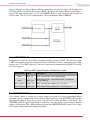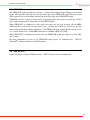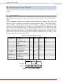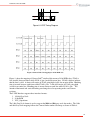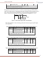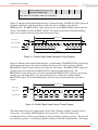
1
Tamarisk®320
17 µm 320x240 Long Wave Infrared Camera
Electrical Interface Control Document
Document No: 1012820
Revision: D
Tamarisk®320 Electrical ICD
©Copyright 2012, DRS TECHNOLOGIES, Inc.- All rights reserved.
13532 N. Central Expressway
Dallas, TX 75243
877.377.4783
www.drsinfrared.com
The contents of this document may not be reproduced in whole or in part without the written
consent of the copyright owner.
NOTICE
ALL STATEMENTS, INFORMATION, AND RECOMMENDATIONS IN THIS MANUAL ARE BELIEVED TO BE ACCURATE BUT ARE
PRESENTED WITHOUT WARRANTY OF ANY KIND. NOTWITHSTANDING ANY OTHER WARRANTY HEREIN, ALL DOCUMENT FILES
AND SOFTWARE ARE PROVIDED “AS IS” WITH ALL FAULTS. DRS DISCLAIMS ALL WARRANTIES, EXPRESSED OR IMPLIED,
INCLUDING, WITHOUT LIMITATION, THOSE OF MERCHANTABILITY, FITNESS FOR A PARTICULAR PURPOSE AND
NONINFRINGEMENT OR ARISING FROM A COURSE OF DEALING, USAGE, OR TRADE PRACTICE.
IN NO EVENT SHALL DRS BE LIABLE FOR ANY INDIRECT, SPECIAL, CONSEQUENTIAL, OR INCIDENTAL DAMAGES, INCLUDING,
WITHOUT LIMITATION, LOST PROFITS OR LOSS OR DAMAGE TO DATA ARISING OUT OF THE USE OR INABILITY TO USE THIS
MANUAL, EVEN IF DRS HAS BEEN ADVISED OF THE POSSIBILITY OF SUCH DAMAGES.
Rev History
Revision Number
Release Date
Description
A
01/24/2013
B
9/5/2013
Derived from Tamarisk 640
version
C
06/09/2014
Prepared for Public Release
D
2/15/2015
Updated PDVO Timing
Initial Release
Camera Link® is a registered trademark of the Automated Imaging Association.
Tamarisk®320 Electrical ICD
TABLE OF CONTENTS
Table of Contents
2
Acronyms and Abbreviations
3
Reference Documentation
4
Safety Instructions
5
1
Scope
6
2
Electrical Interfaces
7
2.1
2.2
2.3
2.4
2.5
2.6
2.7
2.8
3
Interfaces and Timing
3.1
3.2
3.3
3.4
3.5
3.6
4
Base Configuration Electrical Interface ....................................................................... 7
Base Configuration Input Power Specification ............................................................. 9
Base + Feature Board Configuration Electrical Interface ............................................10
Base + Feature Board Configuration Input Power Specification .................................12
UART Interface ..........................................................................................................13
Shutter Control ...........................................................................................................13
GENLOCK .................................................................................................................14
USB_DETECT ...........................................................................................................14
15
LVDS Interface...........................................................................................................15
PARALLEL DIGITAL VIDEO INTERFACE .................................................................18
Analog Video Interface ...............................................................................................23
USB Interface(base + feature only) ............................................................................24
RS-232 Interface(base + feature only) .......................................................................24
Shutter Interface ........................................................................................................24
Electrical Connectors
25
2
Tamarisk®320 Electrical ICD
ACRONYMS AND ABBREVIATIONS
Abbreviation
°C
°F
AGC
BPR
CCA
CL
COMM
CSC
CSCI
CSU
dB
DSP
ESD
E-Zoom
FOV
FPA
ft
G
g
GUI
H
HFOV
I/O
ICD
ICE
ID
IR
IRS
km
LR
LWIR
Description
Celsius
Fahrenheit
automatic gain control
bad pixel replacement
circuit card assembly
center line
communication
Computer Software Component
Computer Software Configuration Item
Computer Software Unit
decibels
digital signal processor
electrostatic discharge
electronic zoom
field of view
Focal Plane Array
feet
gravitational force
gram
graphical user interface
height
horizontal field of view
input/output
Interface Control Document
Image Contrast Enhancement
identification
infrared
Interface Requirements Specification
kilometer
lower right
long-wave infrared
Abbreviation
mm
ms
MSB
MTU
MWIR
NETD
NTSC
NUC
NVTHERM
OEM
OLA
P
POL
psi
Rev
ROI
SC
SWIR
TBD
TCR
TIM
UART
UAV
UFPA
USB
V
VDC
VGA
VOx
W
μm
Description
millimeter
milliseconds
Most Significant Bit
Maximum Transfer Unit
Mid-wave infrared
noise equivalent temperature difference
National Television System Committee
non-uniformity correction
Night Vision Thermal Analysis Tool
original equipment manufacturer
Optical Lens Adapter
probability
polarity
pound per square inch
revision
region of interest
split configuration
Short-wave infrared
To Be Determined
Temperature coefficient of resistance
Thermal Imaging Module
Universal Asynchronous Receiver Transmitter
unmanned aerial vehicle
Un-cooled Focal Plane Array
Universal Serial Bus
Vertical or Voltage
volts direct current
video graphics array
Vanadium Oxide
width or Watt
micron (micrometer)
3
Tamarisk®320 Electrical ICD
REFERENCE DOCUMENTATION
The following documents form part of this specification. In the event of a conflict between
documents referenced herein and the contents of this specification, the contents of this specification
shall be considered a superseding requirement.
Document No: 1012593 Tamarisk®320 User Manual
Document No: 1012819 Tamarisk®320 Software Interface Control Document
Document No: 1012821 Tamarisk®320 Camera Control Software User Guide
Document No: 1003727 Tamarisk®320 Mechanical Interface Control Document
4
Tamarisk®320 Electrical ICD
SAFETY INSTRUCTIONS
NOTIFICATIONS: CAUTION, WARNING AND NOTE
The following is a list of notifications and their accompanying symbol that may be found throught
this document to alert the reader to potential risks and to minimize the potential for personal injury
and or damage to the product. When a notification is present, it is important that the user review and
understand all statements related to the notification before proceeding. If questions arise, please
contact your authorized dealler or DRS Technologies.
Notifications are preceeded by a symbol and followed by highlighted text.
notifications are typically used and are defined below:
Three types of
CAUTION
A caution is a procedure, practice, or condition that, if not strictly followed, may
result in personal injury or damage to the equipment that may impede product
performance.
WARNING
A warning is intended to alert the user to the presence of potentially harmful
circumstances and provide precautionary guidance for mitigating risk of personal
injury and or damage to the product.
NOTE
A note is a statement that clarifies or is used to emphasize important information.
1.
Read all instructions
2.
Keep these instructions for future reference.
3.
Follow all instructions
4.
Heed all warnings.
5.
Do not submerge this apparatus in liquid of any kind.
6.
Clean per recommended instructions using dry non-abrasive cloth.
7.
Do not install near any sources of intense heat such as radiators, furnaces, stoves
or other apparatus that regulary produce excessive heat.
8.
Refer all servicing to qualified service personnel
5
Tamarisk®320 Electrical ICD
1 SCOPE
This document describes the electrical interfaces for the Tamarisk®320 line of 17µm, LWIR OEM
Modules and unless otherwise noted, this document describes all configurations of the module.
Software and mechanical support documentation are described in separate documents See Reference
Documentation for a complete listing.
The Tamarisk®320 product name identifies a family of long-wave infrared video cameras with a 17um
pixel pitch 320 x 240 sensor array and comes in two basic configurations (Base and Base + Feature
Board). Refer to the Tamarisk®320 Users Manual for more information.
In this section, the electrical interfaces for the Base configuration and Base + Feature Board
configuration are described.
Lens
Retaining Ring
Lens Mount
Camera
Housing
Processor Board
60-pin Connector
Figure 1: Tamarisk®320 Base Configuration
The Base configuration provides digital outputs in the form of 8-bit, 14-bit or “YUV Superframe”
parallel digital video (LVCMOS UART), 8-bit, 14-bit, 24-bit RGB or “YUV Superframe” Camera
Link® video, and supports shutter status through a 60-pin connector. Advantages of the Base
configuration include parallel digital video output, reduced size, weight and power requirements.
Lens
Retaining Ring
Lens Mount
Feature Board
Camera
Housing
30-pin Connector
Figure 2: Tamarisk®320 Base + Feature Board Configuration
The Base + Feature Board configuration supports RS232 and USB 2.0 serial control, NTSC and PAL
analog video outputs, digital video output via Camera Link® and accepts a range of input power
voltages from 5-18V through a single 30-pin connector. Advantages of this configuration is that it
provides analog video output, as well as full RS232 or USB 2.0 communication.
The recommended screw to secure the feature board is a .060-80 X .125 pan head screw.
6
Tamarisk®320 Electrical ICD
2
ELECTRICAL INTERFACES
2.1 BASE CONFIGURATION ELECTRICAL INTERFACE
This configuration has no Feature board; the electrical interface is through a 60-pin connector located
on the Processor board see Figure 1: Tamarisk®320 Base Configuration for location. A Board layout
is provided below. For more dimesional information, please refer to Document No: 1003727
Tamarisk®320 Mechanical Interface Control Document. The Tamarisk Camera Link®1 video, digital
video, LVCMOS UART interface, shutter status are supported. See the electrical interface pin-out
listed in Table 1.
60-Pin Connector –J2
Pin 2
Pin 1
Figure 3: Processor Board with Connector Location and Dimensions
Table 1: Electrical Interface Pin-Out for Base Configuration
Pin
Signal
Name
Function
Description
Pin
Signal Name
Function
Description
J2.2
J2.4
J2.6
J2.8
VIN
Power
Primary voltage supply
for the camera/module
(3-5.5V)
J2.10
NC
NA
NA
J2.1
J2.3
J2.5
J2.7
Ground
Power
Primary ground return for
module power.
J2.9
J2.11
Reserved
Reserved
NA
No Connection
1
Camera Link® serial control (LVDS_RDp/LVDS_RDn, LVDS_TDp/LVDS_TDn) are NOT supported in any
configuration, serial control is always provided with the UART control for base configuration.
7
Tamarisk®320 Electrical ICD
Pin
Signal
Name
Function
Description
Pin
Signal Name
Function
Description
No Connection
J2.12
USB_DETECT
Input
USB Control signal
detection. It is
recommended that If
communicating to the
camera via a USB to
serial converter, tie this
pin low. If
communicating to the
camera via RS232 or
another UART, tie this
pin high.
2
LVDS Video output Data 3
J2.14
UART_TX
Output
UART Control Output
LVDS_D2p
LVDS_D2n
Output
LVDS Video output Data 2
J2.16
UART_RX
Input
UART Control Input
J2.25
J2.27
LVDS_D1p
LVDS_D1n
Output
LVDS Video output Data 1
J2.18
Reserved
NA
No Connection
J2.29
J2.31
LVDS_D0p
LVDS_D0n
Output
LVDS Video output Data 0
J2.20
Reserved
NA
No Connection
J2.33
J2.35
LVDS_CLK
p
LVDS_CLK
n
Output
LVDS Video Data output
Clock
J2.22
Reserved
NA
No Connection
J2.37
BDSI_D11
Output
Parallel Digital Data
Output
J2.24
SHUTTER_DR
IVE
Output
High when the
shutter is driven
J2.39
BDSI_D10
Output
Parallel Digital Data
Output
J2.26
SHUTTER_EV
ENT
Output
High during a
calibration event
J2.41
BDSI_D9
Output
Parallel Digital Data
Output
J2.28
Reserved
NA
No Connection
J2.43
BDSI_D8
Output
Parallel Digital Data
Output
J2.30
Reserved
NA
No Connection
J2.45
BDSI_D7
Output
Parallel Digital Data
Output
J2.32
Reserved
NA
No Connection
J2.47
BDSI_D6
Output
Parallel Digital Data
Output
J2.34
Reserved
NA
No Connection
J2.49
BDSI_D5
Output
Parallel Digital Data
Output
J2.36
Reserved
NA
No Connection
J2.51
BDSI_D4
Output
Parallel Digital Data
Output
J2.38
GENLOCK
Input/
Output
Video Genlock signal
master or slave. If not
used, leave floating
J2.53
BDSI_D3
Output
Parallel Digital Data
Output
J2.40
BDSI_PCLK
Output
Parallel Digital Video
Clock
J2.55
BDSI_D2
Output
Parallel Digital Data
Output
J2.42
BDSI_LSYNC
Output
Parallel Digital Video
Line Sync (Active
High)
J2.13
J2.15
Reserved
Reserved
J2.17
J2.19
LVDS_D3p
LVDS_D3n
J2.21
J2.23
NA
Output
2
Unused outputs can be no connects
“No connection” should be left floating.
8
Tamarisk®320 Electrical ICD
Pin
Signal
Name
Function
Description
Pin
Signal Name
Function
Description
J2.57
BDSI_D1
Output
Parallel Digital Data
Output
J2.44
BDSI_FSYNC
Output
Parallel Digital Video
Frame Sync (Active
High)
J2.59
BDSI_D0
Output
Parallel Digital Data
Output
J2.46
BDSI_D13
Output
Parallel Digital Video
Data Output
J2.48
BDSI_D12
Output
Parallel Digital Video
Data Output
J2.50
J2.52
J2.54
VCC_IO
Power
Output
1.8V I/O Supply Output
J2.56
J2.58
J2.60
Ground
Power
Ground
J2
Figure 4: 60-pin Connector – J2
Figure 3 provides the board, mounting hole, and connector (J2) dimensions. All dimensions are in
mils and all dimensions are show at the center of the connector or mounting holes (please see
mechanical ICD listed in reference documentation for all up to date dimensions and drawings).
2.2 BASE CONFIGURATION INPUT POWER SPECIFICATION
The primary voltage input (VIN) for this configuration requires the input voltage to be within the
range from 3.0 to 5.5VDC. There are many readily available commercial power supplies power
adapters, and or batteries/battery packs meeting this voltage range with the current requirements
outlined in Table 2.
Table 2: Base Configuration Input Power Specification
Parameter
Description
Min
Typ
Max
Units
VIN
Input Voltage
3.0
5.0
5.5
V
Icc
Input Current (VIN=5.0)
200
260
mA
Icc with Shutter active*
Input Current RMS during transition
(VIN=5.0)
400
650
mA
VOH LVDX_XXX
VOH High Level Output (2.5V output), IOH
= -1mA
VOL LVDS_XXX
VOL Low Level Output (2.5V output), IOL
= -1mA
VOH UART_TX
VOH High Level Output (1.8V output)
VOL UART_TX
VOL Low Level Output (1.8V output)
VIH UART_RX, GENLOCK
VIH High Level Input (1.8V input)
VIL UART_RX, GENLOCK
VOH BDSI_xx, USB_DETECT,
2.0
V
0.4
1.35
V
V
0.45
V
1.17
2.25
V
VIL Low Level Input (1.8V input
-0.3
0.63
V
VOH High Level Output (1.8V output), IOH
= -2mA
1.35
V
9
Tamarisk®320 Electrical ICD
Parameter
Description
Min
Typ
Max
Units
0.45
V
SHUTTER_DRIVE,
SHUTTER_EVENT,
WE_TEST#, GENLOCK
VOL BDSI_xx, USB_DETECT,
SHUTTER_DRIVE,
SHUTTER_EVENT,
WE_TEST#, GENLOCK
VOL Low Level Output (1.8V output), IOL
= -2mA
* The shutter is typically active for 100 mS closing and 100ms opening.
NOTE
Shutter current demand is instantaneous; care should be taken to provide
bypass capacitance to prevent voltage regulator sag.
The module also provides a 1.8V output that can be used to supply some circuitry on the feature
board for the system. This supply is used to drive all 1.8V outputs from the module.
Table 3: Base Configuration External 1.8V Drive Capability
Parameter
Description
Min
Typ
Max
Units
VCC_IO
I/O Output Voltage
1.71
1.8
1.89
V
Iout
Output Current
50
mA
2.3 BASE + FEATURE BOARD CONFIGURATION ELECTRICAL INTERFACE
The Base + Feature Board configuration supports RS170(NTSC and PAL), Camera Link®1, RS232,
USB, and various input power connection options. Electrical interface is through a 30-pin connector
located near the center of the Feature board, See Figure 2. The electrical interface pin-out for this
connector is detailed in Table 4 below:
Table 4: Electrical Interface for Base and Base +Feature Board Configurations
Pin
Signal Name
Function
Description
J19.1
J19.3
EXTPWR
Power
External Power input 5-18V
J19.5
J19.7
EXTPWR_GND
Power
External Power input ground
J19.2
RS232_RX
Input
RS232 input signal
10
Tamarisk®320 Electrical ICD
Pin
Signal Name
Function
Description
J19.4
RS232_TX
Output
RS232 output signal
J19.6
12V_CL
Power
12V power input
J19.8
GND_CL
Power
12V power input ground
J19.9
J19.11
USBDP
USBDM
Bi-directional
USB Interface
J19.10
J19.12
LVDS_D0n
LVDS_D0p
Output
LVDS Video Data output Data 0
J19.14
J19.16
LVDS_D1n
LVDS_D1p
Output
LVDS Video Data output Data 1
J19.18
J19.20
LVDS_D2n
LVDS_D2p
Output
LVDS Video Data output Data 2
J19.22
J19.24
LVDS_CLKn
LVDS_CLKp
Output
LVDS Video Data output Clock
J19.26
J19.28
LVDS_D3n
LVDS_D3p
Output
LVDS Video Data output Data 3
J19.30
A_VID_OUT
Output
Analog Video Output (RS-170 or NTSC or PAL)
J19.13
USB_5V
Power
USB 5V input power
J19.15
Ground
Power
Ground
J19.17
J19.19
NC
NC
NA
NA
J19.21
J19.23
NC
NC
NA
NA
J19.25
GENLOCK
Bi-directional
Video genlock signal master or slave
J19.27
Ground
Power
Ground
J19.29
Analog Video Ground
Power
Dedicated Analog Video Ground
Figure 5: 30-pin Connector – J19
Camera Link® serial control (LVDS_RDp/LVDS_RDn, LVDS_TDp/LVDS_TDn) are NOT supported in any
configuration, serial control is always provided with the UART control for base + feature board.
11
Tamarisk®320 Electrical ICD
2.4 BASE + FEATURE BOARD CONFIGURATION INPUT POWER SPECIFICATION
There are three ways to supply input power to this configuration; these are detailed in Table 5 below:
Table 5: Configuration 2 Input Power Specification
Input
EXTPWR
12V_CL
USB_5V
Icc w/Shutter
active*
GENLOCK
GENLOCK,
USB_5V
Parameter
Description
Min
Typ
Max
Units
VIN
Input Voltage
4.5
5.0
18
V
Icc
Input Current (VIN=5.0)
220
280
mA
VIN
Input Voltage
12.0
Icc
Input current
92
VIN
Input Voltage
5.0
Icc
Input Current
220
280
mA
Icc
Input Current RMS during transition (VIN=5.0)
400
650
mA
VOH High Level Output (1.8V output)
LVDS_xxx
USBDP
USBDM
V
0.45
1.17
V
V
0.63
5
VOL Low Level Output
mA
V
VIL Low Level Input (1.8V input
VOH High Level Output
RS-232 I/O
117
1.35
VOL Low Level Output (1.8V output)
VIH High Level Input (1.8V input)
V
V
V
-5
V
VIH High Level Input
2.5
25
V
VIL Low Level Input
-25
0.8
V
VOH High Level Output (2.5V output), IOH = -1mA
2.0
VOL Low Level Output (2.5V output), IOL = -1mA
V
0.4
V
VOH High Level Output
2.8
3.6
V
VOL Low Level Output
0
0.3
V
Single Ended Rx Threshold
0.8
2.0
V
Differential Common Mode
0.8
2.5
V
Differential Input Sensitivity
0.2
Driver Output Impedance
V
44
ohms
* The shutter is typically active for 100 mS closing and 100ms opening.
NOTE
Shutter current demand is instantaneous; care should be taken to provide
bypass capacitance to prevent voltage regulator sag.
12
Tamarisk®320 Electrical ICD
Figure 6 illustrates the Feature Board’s different power inputs (on the left) and the 5 Volt output (on
the right) which is an input to the Processor Board. By design, the Feature Board accommodates a
range of DC input voltage from 5 to 18V on EXTPWR. However, only one power input should be
used at a time. The 5V to 18V regulator utilizes a Texas Instruments TPS61170DRVR.
Figure 6: OEAX Board Power Block Diagram
2.5 UART INTERFACE
Command & Control for the module is handled through a standard UART. The interface to the
UART is through the connectors described in Table 2 and Table 6. For base configuration the UART
interface uses 1.8V CMOS logic levels, for base + feture board configuration the full RS-232 voltage
levels are supported.
Table 6: UART Signal Definition Configuration 1 and 2
Configuration
Signal
Description
Base
UART_TX
UART Transmit Data. 1.8V LVCMOS output.
Base
UART_RX
UART Receive Data. 1.8V LVCMOS input. 3.3V tolerant.
(NOT 5V tolerant)
Base + Feature
RS232_TX
UART Transmit Data. Supports full +/- 5V levels
Base + Feature
RS232_RX
UART Receive Data. Supports full +/- 25V input levels
2.6 SHUTTER CONTROL
If an external shutter is desired, two external signals are provided via base configuration 60-pin
connector and base configuration + feature board’s 30 pin connector. The SHUTTER_DRV signal is
high when the shutter is being driven (open or closed) and low when the shutter is not driven. The
SHUTTER_EVENT signal is high during a calibration event; this signal is used to indicate that the
shutter is blocking the FPA. During normal operation the SHUTTER_EVENT signal is low. Refer
to the shutter timing diagram for timing information.
13
Tamarisk®320 Electrical ICD
2.7 GENLOCK
The GENLOCK signal in both base and base + feature board support frame linking to an external
signal. All frame data will start based on the rising edge of the GENLOCK signal. Extra line syncs
will be generated to avoid row burn out until the next rising edge of the GENLOCK signal.
GENLOCK will also support a master mode of operation where the camera system drives a frame
sync to other components or subsystems via the GENLOCK pin.
When GENLOCK is configured in slave mode the frame rate can vary between >0 and 60Hz.
Calibration times will increase at lower frame rates. (A frame rate of 0 Hz is a special case and can
cause unexpected behavior during calibration.) The GENLOCK input signal high time can be as low
as 1% and us much as 99% of the 60Hz frame time of 16.66mS(166uS to 16.5mS).
When GENLOCK is configured in master mode the GENLOCK signal goes high for at least 50nS
once a frame.
For more information on how to set GENLOCK mode please see Document No:
Tamarisk®320 Software Interface Control Document
1012819
2.8 USB_DETECT
Active low signal to indicate USB connection – NOT 5V tolerant in base configuration.
14
Tamarisk®320 Electrical ICD
3
INTERFACES AND TIMING
Timing information for both the Base and Base + Feature Board configurations are described in this
section.
3.1 LVDS INTERFACE
The LVDS interface supports two modes of operation Camera Link mode and YUV Superframe
mode.
Camera Link®mode is typically used to interface to Camera Link® frame grabbers. The LVDS video
interface supports 4 LVDS data pairs and the LVDS clock pair as outputs. The LVDS timing is
shown in Table 7, while the timing diagram is shown in Figure 7 and Figure 8. The LVDS Clock
signal has a non fifty percent duty cycle. It is based on a 7x internal clock. The LVDS Clock is high
for 4 of the 7x clock periods and low for 3. During each clock period 7 bits are transmitted on each
data pair. The bits are transmitted in the order shown in Figure 7 with each pixel value starting in the
middle of the high clock period. The LVDS data window timing is shown in Figure 8. The
maximum delay for the data to become valid after clock and the minimum time data will go invalid
before the clock are also described in Table 7.
Table 7: LVDS Timing and Framing
Number
1
Parameter
Min
Nom
Max
Units
Clock Period
48.6
ns
7x Internal Clock Freq
144
MHz
Bit time
6.94
ns
2
Data no longer valid
before clock
0.4
ns
3
Clock to data valid
0.4
ns
4
Data valid window
#LINES
#PIXELS_CL
#PIXELS_YUV
6.14
ns
Lines per frame
480
Pixels per line in Camera
Link Mode
640
Pixels per line in
YUV_SF mode
1280
1
LVDS CLK
LVDS Dxx
b
1
b
0
b
6
b
5
b
4
b
3
b
2
b
1
b
0
b
6
b
5
Figure 7: LVDS Format Diagram
15
Tamarisk®320 Electrical ICD
b
2
b
1
2
3
4
Figure 8 LVDS Timing Diagram
Figure 9 Camera Link® bit mapping for 24 bit RGB color
Figure 9, shows the mapping of Camera Link® serialized bit stream to 24 bit RGB color. FVAL is
low (invalid) between frames while LVAL is low (invalid) between lines. DVAL is high to indicate
that the data is valid. A frame will consist of FVAL going high (valid) for an entire frame. Blanking
time is inserted between each frame while FVAL is low. A line will consist of LVAL going high
(valid) for an entire line. Blanking time is inserted between each line while LVAL is low. The
amount of horizontal and vertical blanking can change based on operating modes and Camera
revisions.
The LVDS Interface supports three interface formats:
1. 14/8 bit Gray Scale
2. 24 bit RGB
3. YUV_Superframe
The 14bit Gray Scale format is used to support the 14bit and 8bit gray scale data modes. The 14bit
and 8bit Gray Scale mapping follows the Camera Link® standard and maps as shown in Table 8.
16
Tamarisk®320 Electrical ICD
Table 8 Camera Link® Gray Scale and YUV_Superframe Mapping to 24 bit color map
Camera Link®
24 Bit color
YUV
14bit data mode
8bit data mode
Superframe
Mode
G7
Not Used
Not Used
Bit 15
G6
Not Used
Not Used
Bit 14
G5
Bit 13
Bit 7
Bit 13
G4
Bit 12
Bit 6
Bit 12
G3
Bit 11
Bit 5
Bit 11
G2
Bit 10
Bit 4
Bit 10
G1
Bit 9
Bit 3
Bit 9
G0
Bit 8
Bit 2
Bit 8
R7
Bit 7
Bit 1
Bit 7
R6
Bit 6
Bit 0
Bit 6
R5
Bit 5
Not Used
Bit 5
R4
Bit 4
Not Used
Bit 4
R3
Bit 3
Not Used
Bit 3
R2
Bit 2
Not Used
Bit 2
R1
Bit 1
Not Used
Bit 1
R0
Bit 0
Not Used
Bit 0
The 24bit RGB format is used to support the colorization data mode and uses the standard Camera
Link® 24bit RGB format.
In YUV Superframe mode a 16 bit video stream is mapped into the Camera Link® Interface as shown
in Table 8. The YUV Superframe consists of 240 lines with each line containing 640 values. The
first 320 values contain YCbCr generated values for the pixels of that line with the second 320 values
containing the pre-AGC values for that line (currently the pre-AGC values are from the frame before
the current YCbCr frame, this allows time for analytics to analyze the pre-AGC data so additional
overlays can be added to the YCbCr data stream by customer analytics). Figure 10 depicts a YUV
Superframe line. The first Cb and Cr data is generated on the average of the first two pixels. The
second Cb and Cr data is generated on pixels 3 and 4 with all further Cb/Cr pairs calculated in a
relative manner. The Pre-AGC data is LSB aligned so if the Pre-AGC data is only 14 bits it will only
occupy the lower 14 bits of the data path respectively.
For Tamarisk®320 Precision Series cameras, the Pre-AGC data is replaced with per pixel
temperature data in 11.5 format. The 11.5 format is provided in Kelvin is defined as 11 bits of
decimal temperature data with 5 bits of fractional data. See the user manual for the exact temperature
calculation.
17
Tamarisk®320 Electrical ICD
1 Line of Data
Y
1
Y
2
Y
3
Y
4
Y
5
Y
6
Y
7
Y
8
C
b
C
r
C
b
C
r
C
b
C
r
C
b
C
r
...
Y
3
1
9
Y
3
2
0
C
b
C
r
P
r
e
A
G
C
1
P P P P
r r r r
e e e e
A A A A
G G G G
C C C C
2 3 4 5
...
P P
r r
e e
A A
G G
C C
3 3
1 2
9 0
Figure 10 YUV Line Format
3.2 PARALLEL DIGITAL VIDEO INTERFACE
The digital video interface can operate in one of three modes:
1. Parallel Video mode,
2. RS-170 Video mode,
3. YUV Superframe mode.
The Parallel Video mode provides a pixel output clock, Line Sync, Frame Sync and 14-bit data. This
mode is used to directly interface to another digital interface (i.e. a processor such as
https://www.leopardimaging.com/Thermal_IP_Camera_Dev_Ki.html). The parallel digital video interface
supports 8 or 14 bit digital video data. Any post-AGC selected video will be 8 bit data (MSB on
BDSI_D13, LSB on BDSI_D6 from Table 1); Pre-AGC selected video will be 14 bit. For customers
that require pre-AGC video, methods will be provided to select full 14 bit video data (see Document
No: 1012819 Tamarisk®320 Software Interface Control Document).
The default Tamarisk® PDVO interface timing specifies 0.5ns of delay time following the rising
edge of PCLK (see Figure 11 and Table 9). This design works well for designs that latch the data,
frame sync, and line sync on the falling edge of PCLK.
1,3
2
2
Valid Data
Frame/Line Sync
Figure 11: Default Parallel Digital Video Timing Diagram
Table 9: Default Parallel Digital Video Timing
Number
Parameter
1
BDSI_PCLK clock frequency for
30 Hz/60Hz frame rate or 9Hz
2
Clock to Data/Fsync/Lsync valid
after the rising edge of the clock
Min
0.5
Nom
Max
Units
10
40.5
MHz
Clock period – 10
ns
18
Tamarisk®320 Electrical ICD
3
Period of BDSI_PCLK
100
ns
Note: Data will be valid for 10 ns before the rising edge of the next clock.
Note: 30Hz for Tamarisk®640, 60Hz for Tamarisk®320
For applications which latch data, frame sync, and line sync on the rising edge of PCLK, DRS has
added a non-volatile parameter. For customers who require additional hold time beyond the specified
0.5ns, a non-volatile parameter (NV PARAM # 197) has been provided to extend the hold time.
Figure 12 illustrates the parallel digital video output timing when NV PARAM #197 is set to 1.
1
2
Valid Data
Frame/Line Sync
Figure 12: New Parallel Digital Video Timing Diagram
Table 10 through Table 12 shows the timing specification for alternate supported parallel digital
video output modes.
Table 10 Parallel Digital Video Timing 14 or 8 bit data (NV Parameter 197 set to 1)
Number
Parameter
1
BDSI_PCLK clock frequency for
30 Hz/60Hz frame rate or 9Hz
2
Output Delay for Data/Fsync/Lsync
Min
Nom
Max
10
-25
Units
MHz
25
ns
Note: 30Hz for Tamarisk®640, 60Hz for Tamarisk®320
Table 11 Parallel Digital Video Timing RS-170 data (NV Parameter 197 set to 1)
Number
Parameter
1
BDSI_PCLK clock frequency for
30 Hz/60Hz frame rate or 9Hz
2
Output Delay for Data/Fsync/Lsync
Min
Nom
Max
27
-9
Units
MHz
14
ns
Note: 30Hz for Tamarisk®640, 60Hz for Tamarisk®320
Table 12 Parallel Digital Video Timing Superframe™ data (NV Parameter 197 set to 1)
Number
Parameter
1
BDSI_PCLK clock frequency for
30 Hz/60Hz frame rate or 9Hz
Min
Nom
40.5
Max
Units
MHz
19
Tamarisk®320 Electrical ICD
Clock to Data/Fsync/Lsync setup
time before edge of clock
2
-8
10
ns
Note: 30Hz for Tamarisk®640, 60Hz for Tamarisk®320
Figure 13 illustrates the Parallel Digital Interface’s horizontal timing. The BDSI_LSYNC signal will
go high for 320 clocks each line to indicate valid video data is available via the data bus
(BDSI_DATA). The BDSI_LSYNC signal will go low for several BDSI_PCLKs between each line
of data. The number of clocks the BDSI_LSYNC is low between valid lines (horizontal blanking
time) can vary based on the operating mode and camera release.
Valid Video Data
3
BDSI_LSYNC
BDSI_PCLK(10MHz)
BDSI_DATA(13:0)
PCNT
319
PCNT
320
PCNT
1
PCNT
2
PCNT
3
PCNT
4
PCNT
5
PCNT
6
PCNT
316
PCNT
317
PCNT
318
PCNT
319
PCNT
320
320 Pixels
Figure 13: Parallel Digital Video Horizontal Timing Diagram
Figure 14 illustrates the Parallel Digital Interface’s vertical timing. The BDSI_FSYNC signal will go
low between each frame of video data to indicate that the next line of video received while the
BDSI_FSYNC signal is high is the first line of the next video frame. The BDSI_FSYNC signal will
go high at least one clock before the BDSI_LSYNC signal goes high (front porch). The
BDSI_FSYNC signal will go low at least one clock after the BDSI_LSYNC signal goes low for the
last line of a frame (back porch). It is intended for the user to sample these signals with the
BDSI_PCLK signal. The vertical blanking time will vary between operating modes and camera
release.
One Video Frame
H Blanking
BDSI_FSYNC
BDSI_LSYNC
BDSI_DATA(13:0)
Line
240
Line
1
Line
2
Line
3
Line
4
Line
5
Line
237
Line
238
Line
239
Line
240
240 Lines
Figure 14: Parallel Digital Video Vertical Timing Diagram
The default mode on the base configuration will drive RS-170 digital encoding designed to drive a
video codec – for example AD9705 digital to analog converter. (Note: This mode is not
recommended for users that are not planning on driving a Digital to Analog converter.) The data will
be contrived to generate a valid analog signal that conforms to the RS170 specifications. The output
20
Tamarisk®320 Electrical ICD
analog signal adheres to requirements for RS170 NTSC, or one of three PAL modes (see Document
No: 1012819 Tamarisk®320 Software Interface Control Document for information on how to set
PAL modes). The 320x240 image data will be stretched in both directions to more completely fill an
NTSC or PAL display.
Data is driven on BDSI_D9 through BDSI_D0 (10 bits). The data is binary format. BDSI_PCLK,
provides the single ended clock for the D/A conversion at 27 MHz. Example timing is shown in
Figure 15 and Figure 16 for PAL mode, and Figure 17 and Figure 18 for NTSC mode.
1728 Clocks per Line
37
ns
BDSI_PCLK(27MHz)
1727
BDSI_DATA(9:0)
1728
1
2
3
4
5
6
7
9
1403
1404
1405
1406
1726
1727
1728
324 Clocks of Horizontal
Blanking
1404 Clocks of Pixels per line
Figure 15: Parallel RS-170 PAL Video Horizontal Timing Diagram
25 Lines
Vertical
Blanking
25 Lines
Vertical
Blanking
Odd Field Lines
H Blanking
BDSI_DATA(9:0)
Row
480
Row
1
Even Field Lines
H Blanking
Row
3
Row
5
Row
7
ROW
573
ROW
575
Row
2
Row
4
Row
6
240
Row
8
ROW
574
ROW
576
240
BDSI_PCLK(27MHz)
Figure 16: Parallel RS-170 PAL Video Vertical Timing Diagram
1716 Clocks per Line
37
ns
BDSI_PCLK(27MHz)
BDSI_DATA(9:0)
1715
1716
1
2
3
4
5
6
7
9
1407
1408
1409
1410
1714
1715
1716
308 Clocks of Horizontal
Blanking
1408 Clocks of Pixels per line
Figure 17: Parallel RS-170 NTSC Video Horizontal Timing Diagram
22.5 Lines
Vertical
Blanking
22.5 Lines
Vertical
Blanking
Odd Field Lines
H Blanking
BDSI_DATA(9:0)
Row
480
Row
1
Row
3
Even Field Lines
H Blanking
Row
5
Row
7
240
Row
477
Row
479
Row
2
Row
4
Row
6
Row
8
Row
478
Row
480
240
BDSI_PCLK(27MHz)
Figure 18: Parallel RS-170 NTSC Video Vertical Timing Diagram
21
Tamarisk®320 Electrical ICD
In YUV_SuperFrame mode the Parallel Digital Video Interface is formatted with 1280 bytes per line
and 240 lines per frame. The format of Parallel Digital Video Interface is shown in Figure 19 and
Figure 20. Each line contains 320 Y values (one per pixel) interleaved with 160 Cb and 160 Cr
values (Cb and Cr are calculated over 2 adjacent pixels) followed by the Pre-AGC data for the same
line (The Pre-AGC data is the pixel data before any non-linear gains are applied). The format of the
Pre-AGC data is 16 bits sent 8 bits at a time. The 8 bits occupy the bits 13 down to 6 of the BDSI
bus with the most significant bit in bit 13 and the other bits filled in respectively. The lower 8 bits of
a pixel are sent on one clock with the upper 8 bits being sent on the next clock. The 14 bits of raw
data is converted to 16 bits that are LSB aligned – that is bits 15:14 will always be low. The lower
byte of the 14bit raw data is sent first followed by the upper byte. The clock rate while in YUV
SuperFrame mode is 40.5MHz. The amount of blanking time between lines and frames will vary
based on camera mode and revision. The pre-AGC values are from the frame before the current
YCbCr frame. This allows for signal processing on the pre-AGC values prior to enhancements being
added to the YCbCr displayed to a user.
For Tamarisk®320 Precision Series cameras, the Pre-AGC data is replaced with per pixel
temperature data in 11.5 format. The 11.5 format is provided in Kelvin is defined as 11 bits of
decimal temperature data with 5 bits of fractional data. See the user manual for the exact temperature
calculation.
BDSI_FSYNC
BDSI_LSYNC
BDSI_DATA(13:6)
Y
1
Cb
Y2
C
r
C
b
Y3
...
Y
3
1
9
C
b
Y
3
2
0
C
r
Pre
AGC
1
lb
Pre
AGC
1
ub
Pre
AGC
2
lb
Pre
AGC
2
ub
...
Pre
AGC
319
lb
Pre
AGC
319
ub
Pre
AGC
320
lb
Pre
AGC
320
ub
BDSI_FSYNC
Figure 19 YUV SuperFrame Line Format Over Parallel Digital Video Interface
One Video Frame
H Blanking
BDSI_FSYNC
BDSI_LSYNC
BDSI_DATA(13:0)
Line
240
Line
1
Line
2
Line
3
Line
4
Line
5
Line
237
Line
238
Line
239
Line
240
240 Lines
Figure 20 YUV Sperframe Frame Format Over Parallel Digital Video Interface
Table 13: YUV_SuperFrame Video Timing
Number
Parameter
1
BDSI_PCLK clock frequency for
60 Hz, 30 Hz frame rate or 9Hz
2
Clock to Data/Fsync/Lsync valid
after the rising edge of the clock
Min
Nom
Max
40.5
0.5
Units
MHz
Clock period – 10
ns
Note: Data will be valid for 10 ns before the rising edge of the next clock.
22
Tamarisk®320 Electrical ICD
3.3 ANALOG VIDEO INTERFACE
The camera provides an analog video output which follows the RS-170 standard (base + feature
only). The analog video output signal is transmitted at 1v Peak-to-Peak. Following are the nominal
output signal levels when terminated with 75 Ohms (+/- 5%).
Sync tip
-0.284 V
Blank
0V
Black
0.051 V
White
0.714 V
Frame timing parameters are shown in Table 14.
Table 14: Analog Video Timing
RS-170 Out
Quantity
Description
Pixel
line
line blanking
active video
field
vertical blanking
frame
vertical blanking
Active video
Clocks
Rate
time
1
13.5 MHz
74.074 ns
780 total pixels
858
140 blanking pixels
144
640 active pixels
63.556 us
15.734 kHz
10.700 us
640
47.400 us
262.5 lines
225,225
16.683 ms
20 lines
17,160
525 lines
450,450
40 lines
34,320
485 lines
416,130
61.050 Hz
1.271 ms
33.367 ms
30.525 Hz
2.542 ms
30.824 ms
The camera’s FPA outputs an image that has 240 lines that are stretched to 480 lines, but RS-170
specifies 485 lines of active video. The module accommodates this by inserting “black” lines in line
positions 481 through 485 as illustrated in Figure 21.
line 1
line 2
line 3
line 1
line 2
line 3
line4
FPA
Output
frame
RS-170
output
frame
line 480
line 480
line 481
line 482
line 483
line 484
line 485
Figure 21: Analog Video Format
23
Tamarisk®320 Electrical ICD
3.4 USB INTERFACE(BASE + FEATURE ONLY)
The USB interface utilizes FTDI’s FT232RQ. The FT232RQ is a UART to USB Transceiver. For
specific timing information refer to the FTDI data sheet.
3.5 RS-232 INTERFACE(BASE + FEATURE ONLY)
The RS-232 interface utilizes Linear Technologies’ TC2801IDE#PBF. The TC2801IDE#PBF is a
UART to RS-232 Transceiver. For specific timing information refer to the Linear Technologies data
sheet.
3.6 SHUTTER INTERFACE
The shutter is not spring loaded. The shutter is bi stable. If the shutter is closed and the camera is
powered down, the shutter will remain closed until power is applied again. If the shutter is open and
the camera is powered down, the shutter will remain open.
The shutter timing diagram is shown in Figure 22. When the SHUTTER_EVENT signal is high, the
camera’s software is performing calibration. As the camera warms or cools the camera may change
operating ranges. During these operating range changes, the shutter is closed for a longer period of
time.
Table 15: Shutter Timing
Number
Parameter
1
SHUTTER_DRV high time
2
Min
Nom
Max
100
Units
ms
SHUTTER_EVENT high time without a
range change
440
ms
SHUTTER_EVENT high time during a
camera range change
1
s
Figure 22: Shutter Timing
24
Tamarisk®320 Electrical ICD
4
ELECTRICAL CONNECTORS
There are two electrical connectors that support electrical interface to the Tamarisk®640 camera
module, with the connector type being dictated by the model configuration. The connector
manufacturer and part number shown below is the part number which is on the camera board. The
designer must interface to one of these connectors. Please refer to the Tamarisk®640 Users Manual for
more details:
Configuration 1: 60-pin Samtec ST4-30-1-L-D-P-TR. http://www.samtec.com/
Configuration 2: 30-pin JST BM30B-SRDS-G-TF. http://www.jst.com/index.html
25