1
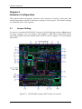
WADE-8041
Mini-ITX Board
User's Manual
P/N: B8981490 Version 1.0
Copyright © Portwell, Inc., 2007. All rights reserved.
All other brand names are registered trademarks of their respective owners.
Preface
Table of Contents
How to Use This Manual
Chapter 1 System Overview.......................................................................................................1-1
1.1 Introduction.................................................................................................................................. 1-1
1.2 Check List ..................................................................................................................................... 1-1
1.3 Product Specification .................................................................................................................. 1-2
1.3.1 Mechanical Drawing......................................................................................................... 1-4
1.4 System Architecture .................................................................................................................... 1-5
Chapter 2 Hardware Configuration ...........................................................................................2-1
2.1 Jumper Setting ............................................................................................................................. 2-1
2.2 Connector Allocation .................................................................................................................. 2-4
Chapter 3 System Installation....................................................................................................3-1
3.1 Intel® Pentium M/Celeron M Processor................................................................................... 3-1
3.2 Main Memory .............................................................................................................................. 3-2
3.3 Installing the Single Board Computer ...................................................................................... 3-2
3.3.1 Chipset Component Driver.............................................................................................. 3-2
3.3.2 Intel Integrated Graphics GMCH Chip .......................................................................... 3-3
3.3.3 Ethernet Controller............................................................................................................ 3-3
3.3.4 Audio Controller ............................................................................................................... 3-3
3.4 Clear CMOS Operation............................................................................................................... 3-4
3.5 WDT Function.............................................................................................................................. 3-4
3.6 GPIO .............................................................................................................................................. 3-6
3.6.1 Pin assignment................................................................................................................... 3-6
3.6.2 WADE-8041 GPIO Programming Guide ....................................................................... 3-7
3.6.3 Example1 ............................................................................................................................ 3-8
Chapter 4 BIOS Setup Information............................................................................................4-1
4.1 Entering Setup.............................................................................................................................. 4-1
4.2 Main Menu ................................................................................................................................... 4-2
4.3 Standard CMOS Setup Menu .................................................................................................... 4-3
4.4 IDE Adaptors Setup Menu......................................................................................................... 4-5
4.5 Advanced BIOS Features............................................................................................................ 4-6
4.6 Advanced Chipset Features ..................................................................................................... 4-10
4.7 Integrated Peripherals .............................................................................................................. 4-12
4.8 Power Management Setup ....................................................................................................... 4-15
4.9 PnP/PCI Configurations .......................................................................................................... 4-19
4.10 PC Health Status...................................................................................................................... 4-20
4.11 Frequency/Voltage Control................................................................................................... 4-20
4.12 Default Menu ........................................................................................................................... 4-21
4.13 Supervisor/User Password Setting ...................................................................................... 4-21
4.14 Exiting Selection ...................................................................................................................... 4-22
Chapter 5 Troubleshooting ........................................................................................................5-1
5.1 Hardware Quick Installation ..................................................................................................... 5-1
5.2 BIOS Setting.................................................................................................................................. 5-1
5.3 FAQ ............................................................................................................................................... 5-3
Appendix A
Appendix B
Preface
How to Use This Manual
The manual describes how to configure your WADE-8041 system board to meet
various operating requirements. It is divided into five chapters, with each chapter
addressing a basic concept and operation of Single Host Board.
Chapter 1 : System Overview. Presents what you have in the box and give you an
overview of the product specifications and basic system architecture for this series
model of single host board.
Chapter 2 : Hardware Configuration. Shows the definitions and locations of Jumpers
and Connectors that you can easily configure your system.
Chapter 3 : System Installation. Describes how to properly mount the CPU, main
memory and Compact Flash to get a safe installation and provides a programming
guide of Watch Dog Timer function.
Chapter 4 : BIOS Setup Information. Specifies the meaning of each setup
parameters, how to get advanced BIOS performance and update new BIOS. In
addition, POST checkpoint list will give users some guidelines of trouble-shooting.
Chapter 5 : Troubleshooting. Provides various useful tips to quickly get WADE-8041
running with success. As basic hardware installation has been addressed in Chapter
3, this chapter will basically focus on system integration issues, in terms of backplane
setup, BIOS setting, and OS diagnostics.
The content of this manual is subject to change without prior notice. These changes
will be incorporated in new editions of the document. Portwell may make
supplement or change in the products described in this document at any time.
Updates to this manual, technical clarification, and answers to frequently asked
questions will be shown on the following web site : http://www.portwell.com.tw/.
System Overview
Chapter 1
System Overview
1.1
Introduction
The WADE-8041 is a cost-effective Mini-ITX embedded board for applications that
need low power consumption. Built with Ultra Low Voltage Intel Celeron M
processors, WADE-8041 generates the computing power necessary for most
embedded applications. Its dual video feature also enables the use of two displays
simultaneously. Its four COM and Six USB ports provide an immediate interface to a
range of peripherals.
WADE-8041 can run with Intel Socket 479 Pentium M / Celeron M processors, and
support DIMM up to 1GB DDR Memory. The enhanced on-board two PCI-IDE
interface can support 4 drives with Ultra ATA33/66/100/133 synchronous mode
feature, the on-board Super I/O chipset support four serial ports. Three RS-232 serial
port interface and one RS-232 pin herder. Besides, it can provide dual display
function by VGA and LVDS interface.
WADE-8041 can support up to two PCI add-on card via riser card. One 6-pin
Mini-DIN connectors are provided to connect PS/2 mouse and keyboard. The
on-board Flash ROM is used to make the BIOS update easier. One 20-pin standard
connector is designed to support ATX power function. All of these features make
WADE-8041 Series excellent in stand-alone applications.
1.2
Check List
The WADE-8041 package should cover the following basic items
One WADE-8041 Mini ITX Board
One 40pin IDE cable
One Parallel Port cable
One I/O Shield
One Installation Resources CD-Title
If any of these items is damaged or missing, please contact your vendor and keep all
packing materials for future replacement and maintenance.
WADE-8041 User’s Manual
1-1
System Overview
1.3
Product Specification
CPU
- Support Intel Pentium Mobile / Celeron M processor
- CPU bus clock : 400 MHz
Chipset Intel® 82852GM GMCH & 82801DB ICH4 Main Memory
- One 184-pin DIMM socket
- Supports up to CL2 or 2.5 or 1 DIMMs at DDR200/DDR266 MHz memory bus.
System BIOS
AWARD BIOS
Super I/O Winboand W83627HG
- Serial Ports : Support Four RS232 ports
- IrDA Interface : Support one Infrared port
Storage IDE Interface
Support Two Ultra DMA 33/66/100/133 support four IDE devices by one 44-pin
and one 40-pin IDE connector, one Compact Flash socket (reverse side)
USB
Support 6 x USB 2.0 ports
Keyboard and PS/2 Mouse Interfaces
Support two mini-DIN 6-pin connectors for Keyboard and Mouse
Auxiliary I/O
- One 2-pin system reset switch
- One 2-pin system power on LED
- One 2-pin HDD active indicator interface
- One 2-pin ATX power control interface
- Two 3-pin headers for CPU and system fan
Real-Time Clock/Calendar (RTC)
- Build-in ICH4
- Y2K compliant
System Monitoring and Protection
Monitoring system temperature, voltage, and cooling fan status
Wake On LAN
Support system wake up function from Network
On-chip VGA Display
- Intel® FW82852GM GMCH integrated Extreme Graphics controller
- One DSUB-15 connector for CRT display interface
- LVDS connectors for up to 24bits LVDS panel display interface
- CRT mode: Support Maximum resolution up to 2048 x 1536
- Multiple Maximum overlay display resolution up to 1600 x 1200
WADE-8041 User’s Manual
1-2
System Overview
On-board Ethernet Function
- Support dual Ethernet function two RJ-45 interface ports, by Realtek (8100C)
Ethernet controller support 10/100BASE-T
- Support two LED indicators to display active and link message
PCI Interfaces
Support up to two PCI slot via riser card
Physical and Environmental requirements :
- Outline Dimension (L x W) : 170mm (6.69 inch) X 170mm (6.69 inch)
- Power Requirements: [email protected] (System), [email protected](CPU),
[email protected](System)
- Operating Temperature : 0 ~ 55 ℃
- Storage Temperature : -20~70℃
- Relative Humidity : 5% to 95%, non-condensing
WADE-8041 User’s Manual
1-3
System Overview
10.59
51.59
163.83
Mechanical Drawing
6.35
1.3.1
165.10
165.10
104.54
63.54
33.02
10.16
25.32
21.74
6.50
143.77
121.99
100.36
163.83
170.00
25.27
6.27
74.22
38.13
11.66
6.35
0.00
0.00
19.00
12.50
6.50
4.00
6.27
WADE-8041 User’s Manual
1-4
System Overview
1.4
System Architecture
All of details operating relations are shown in WADE-8041 System Block Diagram.
WADE-8041 System Block Diagram
WADE-8041 User’s Manual
1-5
Hardware Configuration
Chapter 2
Hardware Configuration
This chapter indicates jumpers’, headers’ and connectors’ locations. Users may find
useful information related to hardware settings in this chapter. The default settings
are indicated with a star sign (Ì).
2.1
Jumper Setting
For users to customize WADE-8041’s features. In the following sections, Short means
covering a jumper cap over jumper pins; Open or N/C (Not Connected) means
removing a jumper cap from jumper pins. Users can refer to Figure 2-1 for the Jumper
allocations.
Figure 2-1 WADE-8041 Jumper and Connector Locations
WADE-8041 User’s Manual
2-1
Hardware Configuration
The jumper settings are listed as follows:
JP1: COM2 RI/power function Selection
JP1
1-2 SHORT
3-4 SHORT
5-6 SHORT
Function
COM2_5V
R2_1 Ì
COM2_12V
JP2: COM2 RS232/RS422/RS485 Function Select
5-6
Short
3-4
Short
1-2
Short
9-11
Short
7-9
Short
7-9
Short
10-12
Short
8-10
Short
8-10
Short
PIN No.
15-17
16-18
Short
Short
13-15
14-16
Short
Short
19-20
Other
Short
Open
Function
Other
Open
21-22
Short
RS-232 Ì
Other
Open
RS-422
RS-485
JP3: COM1 RI/power function Selection
JP3
1-2 SHORT
3-4 SHORT
5-6 SHORT
Function
COM1_5V
RI_1 Ì
COM1_12V
JP4: COM3 RI/power function Selection
JP4
1-2 SHORT
3-4 SHORT
5-6 SHORT
Function
COM3_5V
R3_1 Ì
COM3_12V
JP5: LCD Voltage Setup
PIN No.
1-2
2-3
Short
Open
Open
Short
WADE-8041 User’s Manual
Function
Panel power
+3V TFT LCD Ì
+5V TFT LCD
2-2
Hardware Configuration
JP6: CMOS Setup (1*2 Pin Header)
PIN 1-2
Short
Open
Function
CLEAR CMOS
Normal (Keep CMOS Setup)
JP7: PSB CLOCK
(1-2)
Open
Open
Open
Open
Short
Short
Short
Short
PIN No.
(2-3)
Open
Open
Short
Short
Open
Open
Short
Short
(5-6)
Open
Short
Open
Short
Open
Short
Open
Short
FSB
400
400
400
400
533
533
533
400
Description (MHz)
DDR SDRAM
GRAPHIC
267
133-200
200
100-200
200
100-133
267
133-267
267
133-200
267
133-267
333
167-267
333
167-250
JP8: CPU FSB Setup
PIN No.
1-2
2-3
Short
Open
Open
Short
Description
FSB
Reserved (533MHz)
400MHz Ì
JP9: CF Boot Setup
JP9
SHORT
OPEN
Function
Master Ì
Slave
WADE-8041 User’s Manual
2-3
Hardware Configuration
2.2
Connector Allocation
I/O peripheral devices are connected to the interface connectors
Connector Function List
Connector
J1
J2
J3
J4
J5A
J6A
J5B
J6B
J7
J8
J9
J10
J11
J12
J14
J15
J17
J19
J21
J22
J23
VGA_COM1A
VGA_COMB
LPT1
DIMM
Function
COM1~COM2 (RS-232) connector
PS/2 Keyboard/Mouse connector
Audio Jack
KB/MS Pin header (OPTIONAL)
10/100 LAN1 Connector
10/100 LAN2 Connector
USB (0~1) Connector
USB (2~3) Connector
System Panel Power Button Connectors
Inverter Power Connector
Dual Channel LVDS Connector
USB (4~5) Connector
FAN1 Connector
FAN2 Connector
IDE 2 Interface Connector
IrDA Connector
COM4 (RS-232)
IDE 1 Connector
ATX Power Connector
GPIO Connector
Compact Flash Socket
CRT Connector
COM3 (RS-232)
Printer Port
184 PIN DDR1 DIMM
WADE-8041 User’s Manual
Remark
2-4
Hardware Configuration
VGA_COM1A: CRT Connector
5
1
10
6
15
PIN No.
1
2
3
13
14
11
Description
R
G
B
HSYNC
VSYNC
PIN No.
12
15
7/8
5/10
9
Description
SDA
SCL
GND
GND
VGA_VCC
VGA_COMB: COM3 (RS-232)
PIN No.
C1
C2
C3
C4
C5
Description
-DCD
RX
TX
-DTR
GND
PIN No.
C6
C7
C8
C9
Description
-DSR
-RTS
-CTS
RI3/COM3_VCC
LPT1: Printer Port
PIN No.
1
3
5
7
9
11
13
15
17
19
21
23
25
Description
-STB
PTD0
PTD1
PTD2
PTD3
PTD4
PTD5
PTD6
PTD7
ACK
BUSY
PE
SLCT
WADE-8041 User’s Manual
PIN No.
2
4
6
8
10
12
14
16
18
20
22
24
26
Description
AFD
ERR
INIT
SLIN
GND
GND
GND
GND
GND
GND
GND
GND
GND
2-5
Hardware Configuration
DIMM1: 184 PIN DDR1 DIMM
J1: COM1~COM2 (RS-232)
PIN No.
1
2
3
4
5
11
14
16
18
Description
-NDCD
NRX
NTX
-NDTR
GND
RXD2
GND
RTS2
RI2/COM2_VCC
PIN No.
6
7
8
9
10
13
15
17
Description
-NDSR
-NRTS
-NCTS
RI1/COM1_VCC
DCD2
DTR2
DSR2
CTS2
J2: PS/2 Keyboard/Mouse
PIN No.
1
5
3,9
7
4,10
11
Description
K/B DATA
K/B CLK
GND
MDAT
+5V
MCLK
J3: Audio Jack
PIN No.
1 (Blue)
2 (Lime)
3 (Pink)
Description
Line In
Line Out
Mic In
WADE-8041 User’s Manual
2-6
Hardware Configuration
J4: KB/MS Pin header (OPTIONAL)
PIN No.
1
2
3
4
5
6
Description
K/B DATA
MDAT
GND
+5V
K/B CLK
MCLK
J5A/J6A: 10/100 LAN Connector
PIN No.
1
3
5
7
9
Description
CT
TXRXNC
NC
PIN No.
2
4
6
8
10
Description
TX+
RX+
NC
NC
RXC
PIN No.
5
6
7
8
Description
+5V
USB_D1USB_D1+
GND
PIN No.
5
6
7
8
Description
J5B: USB (0~1) Connector
PIN No.
1
2
3
4
Description
+ 5V
USB_D0USB_D0+
GND
J6B: USB (2~3) Connector
PIN No.
1
2
3
4
Description
+ 5V
USB_D0USB_D0+
GND
WADE-8041 User’s Manual
+5V
USB_D1USB_D1+
GND
2-7
Hardware Configuration
J7: System Panel Power Button Connectors (1*2 Pin Header)
PIN No.
1
2
3
4
5
6
7
8
Description
PW_BN+
PW_BNRESET SW+
RESET SWIDE LED+
IDE LEDPOWER LED+
POWER LED-
J8: Inverter Power Connector (1*5 Pin Wafer)
PIN No.
1
2
3
4
5
Description
BKL_EN
GND
+12V
GND
+5V
J9: Dual Channel LVDS Connector
PIN No.
1
3
5
7
9
11
13
15
17
19
21
23
25
27
29
Description
VDD_CH1
CH1_IYAP0
CH1_IYAP1
CH1_IYAP2
CH1_IYAP3
CH1_ICLKAP
CH1_DCPCLK
GND_ CH1
CH2_IYBP0
CH2_IYBP1
CH2_IYBP2
CH2_IYBP3
CH2_ICLKBP
CH2_DCPCLK
GND_ CH2
WADE-8041 User’s Manual
PIN No.
2
4
6
8
10
12
14
16
18
20
22
24
26
28
30
Description
VDD_CH1
CH1_IYAM0
CH1_IYAM1
CH1_IYAM2
CH1_IYAM3
CH1_ICLKAM
CH1_DCPDATA
GND_ CH1
CH2_IYBM0
CH2_IYBM1
CH2_IYBM2
CH2_IYBM3
CH2_ICLKBM
CH2_DCPDATA
GND_ CH2
2-8
Hardware Configuration
J10: USB (4~5) Connector (2*5 pin Header)
PIN No.
1
3
5
7
9
Description
+ 5V
USB_D5USB_D5+
GND
NC
PIN No.
2
4
6
8
10
Description
+5V
USB_D6+
USB_D6GND
GND
J11/J12: FAN1 and FAN2 (1*3 Pin Box Header)
PIN No.
1
2
3
Description
Fan Speed Detect
+12V
GND
J14: IDE 2 Interface Connector (2*22 Pin Box Header)
PIN No.
1
3
5
7
9
11
13
15
17
19
21
23
25
27
29
31
33
35
37
39
41/42
Description
RESET#
DATA 7
DATA 6
DATA 5
DATA 4
DATA 3
DATA 2
DATA 1
DATA 0
GND
IDRQ
IOW#
IOR#
CHRDY
DACK
INT#
SA1
SA0
CS0#
ACTIVE#
+5V
WADE-8041 User’s Manual
PIN No.
2
4
6
8
10
12
14
16
18
20
22
24
26
28
30
32
34
36
38
40
43/44
Description
GND
DATA 8
DATA 9
DATA 10
DATA 11
DATA 12
DATA 13
DATA 14
DATA 15
N/C
GND
GND
GND
CABLE SELECT
GND
N/C
66DET
SA2
CS1#
GND
GND
2-9
Hardware Configuration
J15: IrDA Connector (1*6 Pin Wafer)
PIN No.
1
2
3
4
5
6
Description
+5V
Reserved
IRRx
GND
IRTx
NC
J17: COM4 (RS-232) (2*5 Pin Header)
PIN No.
1
2
3
4
5
Description
-NDCD
NRX
NTX
-NDTR
GND
PIN No.
6
7
8
9
10
Description
-NDSR
-NRTS
-NCTS
-NRI_
NC
J19: IDE 1 Connector (2*20 Pin Box Header)
PIN No.
1
3
5
7
9
11
13
15
17
19
21
23
25
27
29
31
33
35
37
39
Description
RESET#
DATA 7
DATA 6
DATA 5
DATA 4
DATA 3
DATA 2
DATA 1
DATA 0
GND
DRQ
IOW#
IOR#
CHRDY
DACK
INT#
SA1
SA0
CS0#
ACTIVE#
WADE-8041 User’s Manual
PIN No.
2
4
6
8
10
12
14
16
18
20
22
24
26
28
30
32
34
36
38
40
Description
GND
DATA 8
DATA 9
DATA 10
DATA 11
DATA 12
DATA 13
DATA 14
DATA 15
N/C
GND
GND
GND
CS
GND
N/C
66DET
SA2
CS1#
GND
2-10
Hardware Configuration
J21: ATX Power Connector
J22: GPIO Connector (2*5 Pin Header)
PIN No.
1
3
5
7
9
Description
IO_4
IO_5
IO_6
IO_7
GND
PIN No.
2
4
6
8
10
Description
IO_0
IO_1
IO_2
IO_3
+5V
J23: Compact Flash Socket
PIN No.
1
2
3
4
5
6
7
8
9
10
11
12
13
14
15
16
17
18
19
20
21
22
23
24
25
Description
GND
DATA 3
DATA 4
DATA 5
DATA 6
DATA 7
CS0#
GND
GND
GND
GND
GND
+5V
GND
GND
GND
GND
SA2
SA1
SA0
DATA 0
DATA 1
DATA 2
N/C
N/C
WADE-8041 User’s Manual
PIN No.
26
27
28
29
30
31
32
33
34
35
36
37
38
39
40
41
42
43
44
45
46
47
48
49
50
Description
N/C
DATA 11
DATA 12
DATA 13
DATA 14
DATA 15
CS1
GND
IOR#
IOW#
VCC_COM
IRQ15
+5V
CSEL
N/C
RESET
IORDY
SDREQ
SDACK#
ACTIVE#
PDIAG#
DATA 8
DATA 9
DATA 10
GND
2-11
System Installation
Chapter 3
System Installation
This chapter provides you with instructions to set up your system. The additional
information is enclosed to help you set up onboard PCI device and handle Watch Dog
Timer (WDT) and operation of GPIO in software programming.
3.1
Intel® Pentium M/Celeron M Processor
Installing Socket 479 CPU on actuator (for PGA Processor Type)
Making sure to loosen the latch of actuator at correctly position (Open), and then
configure CPU more gently, don’t be forcible push to do it.
Figure 3-1
Removing CPU
1) Unlock the cooling fan first.
2) Unlock the latch of CPU socket to open position.
3) Carefully lifts up the existing CPU to remove it from the actuator.
4) Follow the steps of installing a CPU to change to another one or drive latch to close
the opened actuator.
Configuring System Bus
WADE-8041 of PGA Type will automatically detect the CPU used. CPU speed of Intel
Pentium M /Celeron M can be detected automatically.
WADE-8041 User’s Manual
3-1
System Installation
3.2
Main Memory
WADE-8041 provides One DIMM socket which supports 200/266 DDR-SDRAM as
main memory, Non-ECC (Error Checking and Correcting), non-register functions.
The maximum memory size can be up to 1GB capacity.
For system compatibility and stability, do not use memory module without brand.
Memory configuration can be either one double-sided DIMM in either one DIMM
socket or two single-sided DIMM in both sockets.
Watch out the contact and lock integrity of memory module with socket, it will
impact on the system reliability. Follow normal procedures to install memory module
into memory socket. Before locking, make sure that all modules have been fully
inserted into the card slots.
3.3
Installing the Single Board Computer
To install your WADE-8041 into standard chassis or proprietary environment, please
perform the following:
Step 1 : Checking all jumpers setting on proper position
Step 2 : Installing and configure CPU and memory module on right position
Step 3 : Placing WADE-8041 into the dedicated position in the system
Step 4 : Attach cables to existing peripheral devices and secure it
WARNING
Please ensure that SBC is properly inserted and fixed by mechanism.
Note:
Please refer to section 3.3.1 to 3.3.4 to install INF/VGA/LAN/Audio drivers.
3.3.1
Chipset Component Driver
The chipset used on WADE-8041 is relatively new which operating systems might not
be able to recognize. To overcome this compatibility issue, for Windows Operating
Systems such as Windows-2000/XP, please install its INF before any of other Drivers
are installed.
WADE-8041 User’s Manual
3-2
System Installation
3.3.2
Intel Integrated Graphics GMCH Chip
Using Intel 82852 GM chipset is the result of new design approach to optimize the
shared memory architecture while maintaining the cost benefits of integration
through Direct AGP and Dynamic Video Memory Technology. With no additional
video adaptor, this onboard video provides the system display output.
With no additional video adaptor, this onboard video will usually be the system
display output. By adjusting the BIOS setting to disable on-board VGA, an add-on
PCI VGA card can take over the system display.
Drivers Support
Please find Springdale GMC driver in the WADE-8041 CD-title. Drivers support
Windows-2000, Windows XP and Linux.
3.3.3
Ethernet Controller
Drivers Support
Please find Realtek 8100C LAN driver in /Ethernet directory of WADE-8041 CD-title.
The drivers support Windows-2000 and Windows-XP.
LED Indicator (for LAN status)
WADE-8041 provides two LED indicators to report Realtek 8100C Ethernet interface
status. Please refer to the table below as a quick reference guide.
8100C
Color
Name of LED
Status
LED
Green
LAN Linked & Active LED
Green
LAN speed LED
Speed
LED
3.3.4
Operation of Ethernet Port
ON
Linked
OFF
Active
(Blinking)
100 Mbps
10 Mbps
Green
Off
Audio Controller
Please find Realtek ALC655 Audio driver form WADE-8041 CD-title. The drivers
support Windows 2000 and XP.
WADE-8041 User’s Manual
3-3
System Installation
3.4
Clear CMOS Operation
The following table indicates how to enable/disable Clear CMOS Function hardware
circuit by putting jumpers at proper position.
JP6
1-2 Short
Open
Function
Clear CMOS contents
Normal Operation Ì
To correctly operate CMOS Clear function, user must turn off the system, shorted JP6
jumper both of pin 1 and pin 2. To clear CMOS contents, please turn the power back
on and turn it off again for AT system, or press the trigger a few times for ATX
system. Removing the jump from JP6 to open and start the system.
3.5
WDT Function
The working algorithm of the WDT function can be simply described as a counting
process. The Time-Out Interval can be set through software programming. The
availability of the time-out interval settings by software or hardware varies from
boards to boards.
WADE-8041 allows users control WDT through dynamic software programming. The
WDT starts counting when it is activated. It sends out a signal to system reset or to
non-maskable interrupt (NMI), when time-out interval ends. To prevent the time-out
interval from running out, a re-trigger signal will need to be sent before the counting
reaches its end. This action will restart the counting process. A well-written WDT
program should keep the counting process running under normal condition. WDT
should never generate a system reset or NMI signal unless the system runs into
troubles.
The related Control Registers of WDT are all included in the following sample
program that is written in C language. User can fill a non-zero value into the
Time-out Value Register to enable/refresh WDT. System will be reset after the
Time-out Value to be counted down to zero. Or user can directly fill a zero value into
Time-out Value Register to disable WDT immediately. To ensure a successful
accessing to the content of desired Control Register, the sequence of following
program codes should be step-by-step run again when each register is accessed.
Additionally, there are maximum 2 seconds of counting tolerance that should be
considered into user’ application program. For more information about WDT, please
refer to Winbond W83627HG-AW data sheet.
WADE-8041 User’s Manual
3-4
System Installation
There are two PNP I/O port addresses that can be used to configure WDT,
1) 0x2E:EFIR (Extended Function Index Register, for identifying CR index number)
2) 0x2F:EFDR (Extended Function Data Register, for accessing desired CR)
Below are some example codes, which demonstrate the use of WDT.
//Step1. Enter W83627HG configuration registers mode:
outportb(0x2E, 0x87);
outportb(0x2E, 0x87);
//* Step2. Pin89 to be WDTO
outportb(0x2E, 0x2b);
outportb(0x2E + 1, 0x04);
//* Step3. Select logic device 8:
outportb(0x2E, 0x07);
outportb(0x2E + 1, 0x08);
//* Step4. Config WDT using second to be unit:
outportb(0x2E, 0xf5);
outportb(0x2E + 1, 0x00);
//* Step5. Set WDT time-out time:
outportb(0x2E, 0xf6);
outportb(0x2E + 1, time_out);
//* Step6. Exit configuration registers mode:
outportb(0x2E, 0xaa);
---------------------------------------------------------------------------------------------------------------Watch dog timer fulfill under DOS Debug mode
(1) Example: Watch dog timer count down by "second"
o 2e,87
o 2e,87
o 2e,07
o 2f,08
o 2e,30
o 2f,01
o 2e,f5
o 2f,00
o 2e,f6
o 2f,14
; select logic device 8
; default active
; select timer by "second"
; Ex: timer=20 seconds; 00 = Watch dog timer time out disabled
WADE-8041 User’s Manual
3-5
System Installation
(2) Example: Watch dog timer count down by "minutes"
o 2e,87
o 2e,87
o 2e,07
o 2f,08
o 2e,30
o 2f,01
o 2e,f5
o 2f,08
o 2e,f6
o 2f,05
3.6
; select logic device 8
; default active
; select timer by "minutes"
; Ex: timer=5 minutes; 00 = Watch dog timer time out disabled
GPIO
The WADE-8041 provides 8 programmable input or output ports that can be
individually configured to perform a simple basic I/O function. Users can configure
each individual port to become an input or output port by programming register bit
of I/O Selection. To invert port value, the setting of Inversion Register has to be
made. Port values can be set to read or write through Data Register.
3.6.1
Pin assignment
J22: General Purpose I/O Connector
PIN No.
1
2
3
4
5
6
7
8
9
10
Signal Description
General Purpose I/O Port 0 (W83627HG GP14)
General Purpose I/O Port 1 (W83627HG GP10)
General Purpose I/O Port 2 (W83627HG GP15)
General Purpose I/O Port 3 (W83627HG GP11)
General Purpose I/O Port 7 (W83627HG GP16)
General Purpose I/O Port 4 (W83627HG GP12)
General Purpose I/O Port 5 (W83627HG GP17)
General Purpose I/O Port 6 (W83627HG GP13)
Ground
+5V
All General Purpose I/O ports can only apply to standard TTL ± 5% signal level
(0V/5V), and each source sink capacity up to 12mA.
WADE-8041 User’s Manual
3-6
System Installation
3.6.2
WADE-8041 GPIO Programming Guide
There are 8 GPIO pins on WADE-8041. These GPIO pins are from SUPER I/O
(W83627GH-AW) GPIO pins, and can be programmed as Input or Output direction.
J22 pin header is for 8 GPIO pins and its pin assignment as following :
J22_Pin1=GPIO4:from SUPER I/O_GPIO10 with Ext. 4.7K PH
J22_Pin2=GPIO0:from SUPER I/O_GPIO11 with Ext. 4.7K PH
J22_Pin3=GPIO5:from SUPER I/O_GPIO12 with Ext. 4.7K PH
J22_Pin4=GPIO1:from SUPER I/O_GPIO13 with Ext. 4.7K PH
J22_Pin5=GPIO6:from SUPER I/O_GPIO14 with Ext. 4.7K PH
J22_Pin6=GPIO2:from SUPER I/O_GPIO15 with Ext. 4.7K PH
J22_Pin7=GPIO7:from SUPER I/O_GPIO16 with Ext. 4.7K PH
J22_Pin8=GPIO3:from SUPER I/O_GPIO17 with Ext. 4.7K PH
<<<<< Be careful Pin9=GND , Pin10=VCC >>>>>
There are several Configuration Registers (CR) of W83627HG-AW needed to be
programmed to control the GPIO direction, and status(GPI)/value(GPO). CR00h ~
CR2F are common (global) registers to all Logical Devices (LD) in W83627HG. CR07h
contains the Logical Device Number that can be changed to access the LD as needed.
LD7 contains the GPIO10~17 registers.
Programming Guide:
Step1: CR2A_Bit [7.2]. P [1,1,1,1,1,1]; to select multiplexed pins as GPIO10~17 pins
Step2: LD7_CR07h.P [07h]; Point to LD7
Step3: LD7_CR30h_Bit0.P1; Enable LD7
Step4: Select GPIO direction, Get Status or output value.
LD7_CRF0h; GPIO17 ~ 10 direction, 1 = input, 0 = output pin
LD7_CRF2h.P [00h]; Let CRF1 (GPIO data port) non-invert to prevent from confusion
LD7_CRF1h; GPIO17~10 data port, for input pin, get status from the related bit, for
output pin, write value to the related bit.
For example,
LD7_CRF0h_Bit4.P0; Let GPIO14 as output pin
LD7_CRF2h_Bit4.P0; Let CRF1_Bit4 non-inverted
LD7_CRF1h_Bit4.P0; Output “0” to GPIO14 pin (J25_Pin6)
LD7_CRF0h_Bit0.P1; Let GPIO10 as input pin
LD7_CRF2h_Bit0.P0; Let CRF1_Bit0 non-inverted
Read LD7_CRF1h_Bit0; Read the status from GPIO10 pin (J25_Pin1)
WADE-8041 User’s Manual
3-7
System Installation
How to access W83627HG CR?
In WADE-8041, the EFER = 002Eh, and EFDR = 002Fh.
EFER and EFDR are 2 IO ports needed to access W83627HG-AW CR.
EFER is the Index Port, EFDR is the Data Port.
CR index number needs to be written into EFER first,
Then the data will be read/written from/to EFDR.
To R/W W83627HG-AW CR, it is needed to Enter/Enable Configuration Mode first.
When completing the programming, it is suggested to Exit/Disable Configuration
Mode.
Enter Configuration Mode: Write 87h to IO port EFER twice.
Exit Configuration Mode: Write AAh to IO port EFER.
3.6.3
Example1
void enter_Superio2_CFG(void)
{
outportb(0x2E, 0x87);
outportb(0x2E, 0x87);
}
void exit_Superio2_CFG(void)
{
outportb(0x2E, 0xAA);
}
void Set_CFG2(unsigned char Addr2,unsigned char Value2)
{
unsigned char d2;
outportb(0x2E, Addr2);
delay(2);
outportb(0x2E +1, Value2);
delay(2);
}
WADE-8041 User’s Manual
3-8
System Installation
unsigned char Get_CFG2(unsigned char Addr2)
{
unsigned char d2;
outportb(0x2E, Addr2);
delay(2);
d2 = inportb(0x2E +1);
delay(2);
return(d2);
}
int main(void)
{
unsigned char d2;
enter_Superio2_CFG();
/* CR2A B7 = 1 selet GPIO Port 1*/
d2 = Get_CFG2(0x2A);
d2 = (d2 & 0x7F) | 0x80;
Set_CFG2(0x2A, d2);
/* IO test loop 1 */
/* Set GPIO Port 1 of Superio 2 Enable */
Set_CFG2(0x07, 0x07);
Set_CFG2(0x30, 0x01);
/* Select logic device 07 of Superio2*/
/* Enable GPIO Port 1 of Superio2*/
/* IO test loop 1 */
/* Set GPIO Port 1 of Superio2 Enable */
Set_CFG2(0x07, 0x07); /* Select logic device 07*/
Set_CFG2(0xF0, 0x0F);
/* GPIO Port 1 of Superio2 is [ooooiiii], o: output, i:input
*/
Set_CFG2(0xF2, 0x00);
/* GPIO Port 1 of Superio2 is non-inversed*/
Set_CFG2(0x07, 0x07);
Set_CFG2(0xF1, 0xFF);
/* Select logic device 07*/
/* Initial back all GPIO Port1 of Superio 2 to hi */
Set_CFG2(0x07, 0x07);
Set_CFG2(0xF1, 0xEF);
Set_CFG2(0x07, 0x07);
d2 = Get_CFG2(0xF1);
/* Select logic device 07*/
/* GP14 of Superio2 -> ~GP10 of Superio2 */
/* Select logic device 07 of Superio2*/
/* get GPIO Port 2 data */
WADE-8041 User’s Manual
3-9
System Installation
if (d2 == 0xEE )
printf("\n GPIO14->10 test ok");
else
printf("\n GPIO14->10 test fail ");
---------------------------------------------------------------------------------------------------------------* Remarks
General Purpose Input/Output Interface (refer to J22)
a. Function description
IOGP10~IOGP17 belong to CMOS level Schmitt-trigger bi-directional pin with pull
up resistor and open-drain output with 12mA sink capability.
b. Process
1. Setup function as GPIO Pin
2. Input Voltage to Input Port
3. Read Output Port value
c. Example Program
Use “Turbo C” program Setup
#include <stdio.h>
#include <dos.h>
int main(void)
{
int x,outdata,indata;
printf("Now output data to GPIO Port ...");
// Enter the extended function mode
outport(0x2e,0x87);
outport(0x2e,0x87);
// GPIO multiplexed pin selection
outport(0x2e,0x2a);
outport(0x2f,0xff);
//GP10 - GP14 enable
// Enable GPIO port1
outport(0x2e,0x30);
outport(0x2f,0xff);
// Select the logical device
outport(0x2e,0x07);
outport(0x2f,0x07);
WADE-8041 User’s Manual
//Enable GPIO function
// Device 7
3-10
System Installation
// GP10 - GP17 I/O select
printf("\nSet Port10 To Port17 input or output :");
scanf("%x",&x);
outport(0x2e,0xf0);
printf("\n x= %x",x);
outport(0x2f,x);
//GP10 - GP17 output
printf("\n Set output data :");
scanf("%x",&x);
// set GP10-GP13 Output data
outport(0x2e,0xf1);
outport(0x2f,x);
indata=inport(0x2f);
printf("\n Get the Port input data =%x \n",indata);
printf("Enter to test Port LED ....\n");
getch();
printf("LED test Now...");
outdata=0x01;
for (x=0;x<20;x++)
{
printf(".");
outport(0x2e,0xf1);
outport(0x2f,outdata);
delay(300);
outport(0x2e,0xf1);
outdata=outdata<<1;
if (outdata==0x10) outdata=0x01;
}
//Exit the extended function mode
outport(0x2e,0xaa);
return 0;
}
WADE-8041 User’s Manual
3-11
System Installation
d. Example Schematics
VCC
VCC
JP1
1
JP5
1
2 IOGP10
3
2 IOGP14
3
HDR 3x1/2.54mm
HDR 3x1/2.54mm
JP2
1
3
5
7
9
J19
2
4
6
8
10
IOGP14
IOGP15
IOGP16
IOGP17
VCC
VCC
HEADER5X2/2.54mm
JP6
1
IOGP10
IOGP11
IOGP12
IOGP13
R1
200
1
2 IOGP15
2 IOGP11
3
3
HDR 3x1/2.54mm
HDR 3x1/2.54mm
JP3
JP7
1
IOGP10 D1
LED
R2
200
IOGP11 D2
LED
R3
200
IOGP12 D3
LED
R4
200
IOGP13 D4
LED
R5
200
IOGP14 D5
LED
R6
200
IOGP15 D6
LED
R7
200
IOGP16 D7
LED
R8
200
IOGP17 D8
LED
R9
200
1
2 IOGP12
3
2 IOGP16
3
HDR 3x1/2.54mm
HDR 3x1/2.54mm
JP4
JP8
1
1
2 IOGP13
3
HDR 3x1/2.54mm
2 IOGP17
3
HDR 3x1/2.54mm
e. Procedures
i) Run Program while show “Set Port10 To Port17 input or output:” Enter value:
F0 (Setup IOGP10~ IOGP13 as output, IOGP14~ IOGP17 as input)
ii) JP5, JP6, JP7 Switch to VCC; JP8 Switch to GND; LED D8 will light on
iii) While show “Set output data:” Enter value: 7; LED D4 will light on. Then will
show “Get the Port input data =77”
iv) While show “Enter to test Port LED”, press the “Enter” key; will light off the
LED (from D5 to D8) 5 times by sequence.
WADE-8041 User’s Manual
3-12
BIOS Setup Information
Chapter 4
BIOS Setup Information
WADE-8041 is equipped with the AWARD BIOS stored in Flash ROM. These BIOS
has a built-in Setup program that allows users to modify the basic system
configuration easily. This type of information is stored in CMOS RAM so that it is
retained during power-off periods. When system is turned on, WADE-8041
communicates with peripheral devices and checks its hardware resources against the
configuration information stored in the CMOS memory. If any error is detected, or
the CMOS parameters need to be initially defined, the diagnostic program will
prompt the user to enter the SETUP program. Some errors are significant enough to
abort the start-up.
4.1
Entering Setup
Turn on or reboot the computer. When the message “Hit <DEL> if you want to run
SETUP” appears, press <Del> key immediately to enter BIOS setup program.
If the message disappears before you respond, but you still wish to enter Setup,
please restart the system to try “COLD START” again by turning it OFF and then
ON, or touch the "RESET" button. You may also restart from “WARM START” by
pressing <Ctrl>, <Alt>, and <Delete> keys simultaneously. If you do not press the
keys at the right time and the system will not boot, an error message will be displayed
and you will again be asked to,
Press <F1> to Run SETUP or Resume
In HIFLEX BIOS setup, you can use the keyboard to choose among options or modify
the system parameters to match the options with your system. The table below will
show you all of keystroke functions in BIOS setup.
↑↓→ ←
Enter
+ / - /PU /PD
ESC
F1
F2
F5
F6
F7
F9
F10
General Help
: Move
: Select
: Value
: Exit
: General Help
: Item Help
: Previous Values
: Fail-Safe Defaults
: Optimized Defaults
: Menu in BIOS
: Save
WADE-8041 User’s Manual
4-1
BIOS Setup Information
4.2
Main Menu
Once you enter WADE-8041 AWARD BIOS CMOS Setup Utility, a Main Menu is
presented. The Main Menu allows user to select from eleven setup functions and two
exit choices. Use arrow keys to switch among items and press <Enter> key to accept
or bring up the sub-menu.
Phoenix- AwardBIOS CMOS Setup Utility
f Standard CMOS Features
f Advanced BIOS Features
f Advanced Chipset Features
f Integrated Peripherals
f Power Management Setup
f PnP/PCI Configurations
f PC Health Status
f Frequency/Voltage Control
Load Fail-Safe Defaults
Load Optimized Defaults
Set Supervisor Password
Set User Password
Save & Exit Setup
Exit Without Saving
ESC : Quit F9 : Menu in BIOS
F10 : Save & Exit Setup
↑ ↓ → ← : Select Item
Time, Date, Hard Disk Type …
Note:
It is strongly recommended to reload Optimum Setting if CMOS is lost or BIOS is
updated.
WADE-8041 User’s Manual
4-2
BIOS Setup Information
4.3
Standard CMOS Setup Menu
This setup page includes all the items in standard compatible BIOS. Use the arrow
keys to highlight the item and then use the <PgUp>/<PgDn> or <+>/<-> keys to
select the value or number you want in each item and press <Enter> key to certify it.
Follow command keys in CMOS Setup table to change Date, Time, Drive type, and
Boot Sector Virus Protection Status.
Phoenix- AwardBIOS CMOS Setup Utility
Standard CMOS Features
Date (mm:dd:yy)
Time (hh:mm:ss)
f IDE Primary Master
f IDE Primary Slave
f IDE Secondary Master
f IDE Secondary Slave
Tur, April 10 2007
10 : 20 : 30
[None]
[None]
[None]
[None]
Video
[EVG/VGA]
Base Memory
Extended Memory
Total Memory
640K
252928K
253952K
Item Help
Menu Level
f
Change the day, month,
year and century
↑↓→←: Move Enter: Select +/-/PU/PD: Value F10: Save ESC: Exit F1: General Help
F5: Previous Values
F6: Fail-Safe Defaults
F7: Optimized Defaults
Note:
Oblique parameters are base on memory capacity which user adopts on single board.
WADE-8041 User’s Manual
4-3
BIOS Setup Information
Menu Selections
Item
Options
Date
mm:dd:yy
Time
IDE Primary
Master
IDE Primary
Slave
IDE Secondary
Master
IDE Secondary
Slave
Video
Base Memory
Extended
Memory
Total Memory
hh:mm:ss
Description
Change the day, month, year and
century
Change the internal clock
Options are in its sub
menu (described in
Table of section 4.4)
Press <Enter> to enter the sub menu of
detailed options
EGA/VGA
CGA 40
CGA 80
MONO
640K
Select the default video device
N/A
N/A
WADE-8041 User’s Manual
Displays the amount of conventional
memory detected during boot up
Displays the amount of extended
memory detected during boot up
Displays the total memory available in
the system
4-4
BIOS Setup Information
4.4
IDE Adaptors Setup Menu
The IDE adapters control the IDE devices, such as hard disk drive or CD-ROM drive.
It uses a separate sub menu to configure each hard disk drive.
Phoenix- AwardBIOS CMOS Setup Utility
IDE Primary/Secondary Master (&Slave)
IDE HDD Auto-Detection
[Press Enter]
IDE Channel 0 Master
Access Mode
[Auto]
[Auto]
Capacity
0 MB
Cylinder
Head
Precomp
Landing Zone
Sector
0
0
0
0
0
Item Help
Menu Level
f
To atuo-detect the HDD’s
size, head … on this
channel
↑↓→←: Move Enter: Select +/-/PU/PD: Value F10: Save ESC: Exit F1: General Help
F5: Previous Values
F6: Fail-Safe Defaults
F7: Optimized Defaults
Note:
The oblique items are meaning base on what kind of storage device user employs.
Menu Selections
Item
Options
IDE HDD
Press Enter
Auto-detection
IDE Primary/
None
Secondary
Auto
Master or Slave Manual
Access Mode
Capacity
CHS, LBA
Large, Auto
Auto Display your
disk drive size
Description
Press Enter to auto-detect the HDD on this
channel. If detection is successful, it fills
the remaining fields on this menu.
Selecting ‘manual’ lets you set the
remaining fields on this screen. Selects the
type of fixed disk. "User Type" will let you
select the number of cylinders, heads, etc.
Note: PRECOMP=65535 means NONE !
Choose the access mode for this hard disk
Disk drive capacity (Approximated). Note
that this size is usually slightly greater than
the size of a formatted disk given by a disk
checking program.
The following options are selectable only if the ‘IDE Primary Master’ item is set to
‘Manual’
Cylinder
Min=0, Max=65535 Set the number of cylinders for hard disk
Head
Min=0, Max=255
Set the number of read/write heads
WADE-8041 User’s Manual
4-5
BIOS Setup Information
Precomp
Min=0, Max=65535
Landing zone
Sector
Min=0, Max=65535
Min=0, Max=255
4.5
**** Warning: Setting a value of 65535
means no hard disk
****
Number of sectors per track
Advanced BIOS Features
This section allows user to configure your system for basic operation. The system’s
default speed, boot-up sequence, keyboard operation, shadowing and security may
be modified accordingly.
Phoenix- AwardBIOS CMOS Setup Utility
Advanced BIOS Features
f CPU Feature
Virus Warning
CPU L1 & L2 Cache
Quick Power On Self Test
First Boot Device
Second Boot Device
Third Boot Device
Boot Other Device
Boot up NumLock Status
Gate A20 Option
Typematic Rate Setting
X Typematic Rate (Chars/Sec)
X Typematic Delay (Msec)
Security Option
APIC Mode
MPS Version Control For OS
OS Select For DRAM > 64MB
Small Logo(EPA) Show
[Press Enter]
[Disabled]
[Enabled]
[Enabled]
[HDD-0]
[CDROM]
[LS120]
[Enabled]
[On]
[Normal]
[Disabled]
6
250
[Setup]
[Enabled]
[1.4]
[Non-OS2]
[Disabled]
Item Help
Menu Level
f
↑↓→←: Move Enter: Select +/-/PU/PD: Value F10: Save ESC: Exit F1: General Help
F5: Previous Values
F6: Fail-Safe Defaults
F7: Optimized Defaults
WADE-8041 User’s Manual
4-6
BIOS Setup Information
Phoenix- AwardBIOS CMOS Setup Utility
CPU Feature
Thermal Management
Thermal Monitor 1
Item Help
Menu Level f
Set Limit CPUID MaxUal
to 3, Should Be “Disabled”
for WinXP
↑↓→←: Move Enter: Select +/-/PU/PD: Value F10: Save ESC: Exit F1: General Help
F5: Previous Values
F6: Fail-Safe Defaults
F7: Optimized Defaults
Virus Warning
Allow you to choose the VIRUS warning feature for IDE Hard Disk boot sector
protection. If this function is enabled and someone attempt to write data into this
area, BIOS will show a warning message on screen and alarm beep.
Enabled
Disabled
Activates automatically when the system boots up causing a
warning message to appear when anything attempts to access the
boot sector or hard disk partition table.
No warning message will appear when anything attempts to access
the boot sector or hard disk partition table.
CPU L1/L2 Cache
These two categories speed up memory access.
CPU/chipset design.
Enabled
Disabled
However, it depends on
Enable cache
Disable cache
Quick Power On Self Test
Allows the system skip certain tests while booting. This will decrease the time needed
to boot the system.
Enabled
Disabled
Enable quick POST
Normal POST
First/Second/Third Boot Device
Select your Boot Device Priority.
The choice: Floppy, LS120, Hard Disk, CDROM, ZIP 100, USB-FDD, USB-ZIP,
USB-CDROM, LAN and Disabled.
WADE-8041 User’s Manual
4-7
BIOS Setup Information
Boot Other Device
Select your Boot Device Priority.
The choice: Enabled, Disabled.
Boot Up Floppy Seek
Enabled tests floppy drives to determine whether they have 40 or 80 tracks.
The choice: Enabled, Disabled.
Boot Up NumLock Status
Select power on state for NumLock.
The choice: Off, On.
Gate A20 Option
Fast-lets chipsets control Gate A20 and Normal – a pin in the keyboard controller
controls Gate A20. Default is fast.
The choice: Normal, Fast.
Typematic Rate Setting
Keyboard repeat at a rate determined by the keyboard controller, when enabled, the
typematic delay can de select.
The choice: Enabled, Disabled.
※Typematic Rate (Chars/sec)
The rate is which character repeats when you hold down a key at.
The choice: 6, 8, 10, 12, 15, 20, 24, and 30. (Default 6)
※Typematic delay (Msec)
The delay before keystrokes begin to repeat.
The choice: 250, 500, 750, and 1000. (Default 250)
WADE-8041 User’s Manual
4-8
BIOS Setup Information
Security Option
Select whether the password is required every time the system boots or only when
you enter setup.
System
Setup
The system will not boot and access to Setup will be denied if the
correct password is not entered at the prompt.
The system will boot, but access to Setup will be denied if the correct
password is not entered at the prompt.
Note:
To disable security, select PASSWORD SETTING at Main Menu and then you will be
asked to enter password. Do not type anything and just press <Enter>, it will disable
security. Once the security is disabled, the system will boot and you can enter Setup
freely.
APIC Mode
The choice: Enabled, Disabled.
MPS Version Control For OS
The choice: 1.1, 1.4
OS Select For DRAM > 64MB
Select OS/2 only if you are running OS/2 operating system with greater than 64MB
of RAM on the system.
The choice: Non-OS2, OS2.
Small Logo (EPA) Show
Enabled
Disabled
The EPA logo will appear during system boot-up.
The EPA logo will not appear during system boot-up.
WADE-8041 User’s Manual
4-9
BIOS Setup Information
4.6
Advanced Chipset Features
This section allows user to configure the system based on the specific features of the
Intel 82852GM GMCH and 82801DB ICH4 chipsets for WADE-8041. This chipset
manages bus speeds and access to system memory resources, such as DRAM (DDR
SDRAM) and the external cache. It must be stated that these items should never need
to be altered. The default settings have been chosen because they provide the best
operating conditions for the system. The only time user might consider making any
changes would be if you discovered that data was being lost while during system
operation.
Phoenix- AwardBIOS CMOS Setup Utility
Advanced Chipset Features
DRAM Timing Selection
X CAS latency Time
X Active to Precharge Delay
X DRAM RAS# to CAS# Delay
X DRAM RAS# Precharg
DRAM Data Integrity Mode
System BIOS Cacheable
Video BIOS Cacheable
Memory Hole At 15M-16M
Delay transaction
Delay Prior to Thermal
AGP Aperture Size (MB)
*** On-Chip VGA Setting ***
On-Chip VGA
On-Chip Frame Buffer Size
Boot Display
Panel Scaling
Panel Type
FWH Write Protection
[By SPD]
2.5
7
3
3
Non-ECC
[Enabled]
[Disabled]
[Disabled]
[Enabled]
[16 Min]
[64]
Item Help
Menu Level
f
[Enabled]
[32MB]
[CRT]
[Auto]
[640×480 18bit 1ch]
[Enabled]
↑↓→←: Move Enter: Select +/-/PU/PD: Value F10: Save ESC: Exit F1: General Help
F5: Previous Values
F6: Fail-Safe Defaults
F7: Optimized Defaults
DRAM Timing Selection
The choice: By SPD, Manual.
System BIOS Cacheable
The choice: Enabled, Disabled.
WADE-8041 User’s Manual
4-10
BIOS Setup Information
Video BIOS Cacheable
The choice: Enabled, Disabled.
Memory Hole At 15M-16M
The choice: Enabled, Disabled.
Delay Transaction
The choice: Enabled, Disabled.
Delay Prior to Thermal
The choice: 4 Min, 8 Min, 16 Min, 32 Min.
AGP Aperture Size (MB)
The choice: 4, 8, 16, 32, 64, 128, 256
On Chip VGA
The choice: Enabled, Disabled.
On Chip Frame Buffer Size
The choice: 1 MB, 4 MB, 8 MB, 16 MB, 32 MB.
Boot Display
The choice: CRT, LVDS, CRT+LVDS, DVI, CRT+DVI.
Panel Scaling
The choice: Auto, On, OFF.
Panel Type
The choice: 640x480 18bit 1ch, 800x600 18bit 1ch, 1027x768 18bit 1ch, 1400x1050 18bit
2ch
FWH Write Protection
The choice: Enabled, Disabled.
WADE-8041 User’s Manual
4-11
BIOS Setup Information
4.7
Integrated Peripherals
Phoenix- AwardBIOS CMOS Setup Utility
Integrated Peripherals
f OnChip IDE Device
f Onboard Device
f Super IO Device
Watch Dog Timer Select
[Press Enter]
[Press Enter]
[Press Enter]
[Disabled]
Item Help
Menu Level
f
↑↓→←: Move Enter: Select +/-/PU/PD: Value F10: Save ESC: Exit F1: General Help
F5: Previous Values
F6: Fail-Safe Defaults
F7: Optimized Defaults
Phoenix- AwardBIOS CMOS Setup Utility
OnChip IDE Device
On-Chip Primary PCI IDE
IDE Primary Master PIO
IDE Primary Slave PIO
IDE Primary Master UDMA
IDE Primary Slave UDMA
On-Chip Secondary PCI IDE
IDE Secondary Master PIO
IDE Secondary Slave PIO
IDE Secondary Master UDMA
IDE Secondary Slave UDMA
[Enabled]
[Auto]
[Auto]
[Auto]
[Auto]
[Enabled]
[Auto]
[Auto]
[Auto]
[Auto]
IDE HDD Block Mode
[Disabled]
Item Help
Menu Level
f
If your IDE hard drive
supports block mode select
Enabled for automatic
detection of the optimal
number of block
read/writes per sector the
drive can support.
↑↓→←: Move Enter: Select +/-/PU/PD: Value F10: Save ESC: Exit F1: General Help
F5: Previous Values
F6: Fail-Safe Defaults
F7: Optimized Defaults
On-Chip Primary/Secondary PCI IDE
The choice: Enabled, Disabled
IDE Primary/Secondary Master/Slave PIO
The four IDE PIO (Programmed Input/Output) fields allow set a PIO mode (0-4) for
each of the four IDE devices that the onboard IDE interface supports. Modes 0
through 4 provide successively increased performance. In Auto mode, the system
automatically determines the best mode for each device.
The choice: Auto, Mode 0, Mode 1, Mode 2, Mode 3, Mode 4.
WADE-8041 User’s Manual
4-12
BIOS Setup Information
IDE Primary/Secondary Master/Slave UDMA
Ultra DMA/33/66/100 implementation is possible only if IDE hard drive supports
and the operating environment includes a DMA driver (Windows 95 OSR2 or a
third-party IDE bus master driver). If your hard drive and system software both
support Ultra DMA/33/66/100, select Auto to enable BIOS support.
The choice: Auto, Disabled.
IDE HDD Block Mode
If IDE hard drive supports block mode select Enabled for automatic detection of the
optimal number of block read/writes per sector the drive can support.
The choice: Enabled, Disabled.
Onboard Device
Phoenix- AwardBIOS CMOS Setup Utility
OnBoard Device
USB Controller
USB 2.0 Controller
USB Keyboard Support
USB Mouse Support
AC97 Audio
Init Display First
[Enabled]
[Enabled]
[Enabled]
[Disable]
[Auto]
[PCI Slot]
Item Help
Menu Level
f
↑↓→←: Move Enter: Select +/-/PU/PD: Value F10: Save ESC: Exit F1: General Help
F5: Previous Values
F6: Fail-Safe Defaults
F7: Optimized Defaults
USB and USB 2.0 Controller
[Enabled] or [Disabled] universal host controller interface for universal serial bus.
The choice: Enabled, Disabled.
USB Keyboard/Mouse Support
Legacy support of USB keyboard or mouse.
The choice: Disabled, Enabled.
WADE-8041 User’s Manual
4-13
BIOS Setup Information
SuperIO Device Setting
Phoenix- AwardBIOS CMOS Setup Utility
SuperIO Device
Onboard Serial Port 1
Onboard Serial Port 2
UART Mode Select
X RxD, TxD Active
X IR Transmission Delay
X UR2 Duplex Mode
X Use IR Pins
Onboard Parallel Port
Parallel Port Mode
X EPP Mode Select
X ECP Mode Use DMA
PWRON after PWR-Fail
Onboard Serial Port 3
Serial Port Use IRQ
Onboard Serial Port 4
Serial Port Use IRQ
[3F8/IRQ4]
[2F8/IRQ3]
[Normal]
Hi, Lo
Enabled
Half
IR-Rx2Tx2
[378/IRQ7]
[SPP]
EPP 1.7
3
[Off]
[3E8]
[IRQ10]
[2E8]
[IRQ11]
Item Help
Menu Level
f
↑↓→←: Move Enter: Select +/-/PU/PD: Value F10: Save ESC: Exit F1: General Help
F5: Previous Values
F6: Fail-Safe Defaults
F7: Optimized Defaults
UART Mode Select
The choice: IrDA, ASKIR, Normal.
Parallel Port Mode
The choice: SPP, EPP, ECP, ECP+EPP, Normal.
PWRON After PWR-Fail
This item allows user to configure the power status of using ATX power supply after
a serious power loss occurs.
On
Off
System automatically restores Power back
System stays at Power-Off
Watch Dog Timer Select
The choice: Disabled, 10/20/30/40 sec, 1/2/4 Min.
WADE-8041 User’s Manual
4-14
BIOS Setup Information
4.8
Power Management Setup
The Power Management Setup allows configuration of the system to most effectively
save energy while operating in a manner consistent with your own style of computer
use.
Phoenix- AwardBIOS CMOS Setup Utility
Power Management Setup
ACPI Function
ACPI Suspend Type
X Run VGABIOS if S3 Resume
Power Management
Video Off Method
Video Off In Suspend
Suspend Type
Suspend Mode
HDD Power Down
Soft-Off by PWR-BTTN
CPU THRM-Throttling
Wake-Up by Onboard LAN
Power On by Ring
X USB KB Wake-UP From S3
Resume by Alarm
X Date(of Month) Alarm
X Time(hh:mm:ss) Alarm
[Enabled]
[S3(STR)]
No
[User Define]
[DPMS]
[Yes]
[Stop Grant]
[Disabled]
[Disabled]
[Instant-Off]
[50.0%]
[Enabled]
[Enabled]
Disabled
[Disabled]
0
0 : 0 :0
Item Help
Menu Level
f
** Reload Global Timer Events **
Primary IDE 0
[Disabled]
Primary IDE 1
[Disabled]
Secondary IDE 0
[Disabled]
Secondary IDE 1
[Disabled]
FDD,COM,LPT Port
[Disabled]
PCI PIRQ[A-D]#
[Disabled]
↑↓→←: Move Enter: Select +/-/PU/PD: Value F10: Save ESC: Exit F1: General Help
F5: Previous Values
F6: Fail-Safe Defaults
F7: Optimized Defaults
ACPI Function
This item allows you to enable/disable the Advanced Configuration and Power
Management (ACPI).
The choice: Enabled, Disabled.
WADE-8041 User’s Manual
4-15
BIOS Setup Information
ACPI Suspend Type
To decide which ACPI suspend mode to use.
The choice: S3 (STR) only.
※Run VGA BIOS if S3 Resume
The choice: Auto, Yes, No. (Default No)
Power Management
This category allows selecting the type (or degree) of power saving and is directly
related to “HDD Power Down”, “Suspend Mode”.
There are three selections for Power Management, three of which have fixed mode
settings.
Min. Power Saving
Max. Power Saving
User Defined
Minimum power management. Suspend Mode = 1 Hour,
and HDD Power Down = 15 Min.
Maximum power management. Suspend Mode = 1 Min.,
and HDD Power Down = 1 Min.
Allows you to set each mode individually. When not
disabled, Suspend Mode ranges from 1 min. to 1 Hour and
HDD Power Down ranges from 1 Min. to 15 Min.
Video off Method
This determines the manner in which the monitor is blanked.
V/H SYNC+Blank
Blank Screen
DPMS
This selection will cause the system to turn off the vertical
and horizontal synchronization ports and write blanks to
the video buffer.
This option only writes blanks to the video buffer.
Initial display power management signaling.
Video Off In Suspend
This allows user to enable/disable video off in Suspend Mode.
The choice: Yes, No.
Suspend Type
Two options are available : Stop Grant and PWROn Suspend.
The choice: Stop Grant, PWROn Suspend.
WADE-8041 User’s Manual
4-16
BIOS Setup Information
Suspend Mode
When enabled and after the set time of system inactivity, all devices except the CPU
will be shut off.
The choice: Disabled, 1 Min, 2 Min, 4 Min, 8 Min, 12 Min, 20 Min, 30 Min, 40 Min, 1
Hour.
HDD Power Down
When enabled and after the set time of system inactivity, the hard disk drive will be
powered down while all other devices remain active.
The choice: Disabled, 1 Min, 2 Min, 3 Min, 4 Min, 5 Min, 6 Min, 7 Min, 8 Min, 9 Min, 10
Min, 11 Min, 12 Min, 13 Min, 14 Min, 15 Min.
Soft-Off by PWR-BTTN
This item allows users to set the time to remove the power after the power button is
pressed.
The choice: Instant-Off, Delay 4 Sec.
CPU THRM-Throttling
The choice: 87.5%, 75.5%, 62.5%, 50.0%, 37.5%, 25.0%, 12.5%.
Wake-Up By Onboard LAN
The choice: Disabled, Enabled.
Power On by Ring
When select “Enabled”, a system that is at soft-off mode will be alert to
Wake-On-Modem or Wake-On LAN.
The choice: Enabled, Disabled.
※USB KB Wake-Up From S3
The choice: Enabled, Disabled. (Default Disabled)
Resume by Alarm
This item allows users to enable/disable the resume by alarm function. When
“Enabled” is selected, system using ATX power supply could be powered on if a
customized time and day is approached.
The choice: Enabled, Disabled.
WADE-8041 User’s Manual
4-17
BIOS Setup Information
※Date(of Month) Alarm
When “Resume by Alarm” is enabled, this item could allow users to configure the
date parameter of the timing dateline on which to power on the system.
The choice: 0 ~ 31.
※Time (hh:mm:ss) Alarm
When “Resume by Alarm” is enabled, this item could allow users to configure the
time parameter of the timing dateline on which to power on the system.
The choice: hh (0~23), mm (0~59), ss (0 ~59).
Primary/Secondary IDE 0/1
This item is to configure IDE devices being monitored by system so as to keep system
out of suspend mode if the associated device is busy.
The choice: Enabled, Disabled.
FDD, COM, LPT Port
This item is to configure floppy device, COM ports, and parallel port being monitored
by system so as to keep system out of suspend mode if the associated device is busy.
The choice: Enabled, Disabled.
PCI PIRQ[A-D]#
This option can be used to detect PCI device activities. If they are activities, the
system will go into sleep mode.
The choice: Enabled, Disabled.
WADE-8041 User’s Manual
4-18
BIOS Setup Information
4.9
PnP/PCI Configurations
This section describes configuring the PCI bus system. PCI, or Peripheral Computer
Interconnect, is a system which allows I/O devices to operate at speeds nearing the
speed the CPU itself uses when communicating with its own special components.
This section covers some very technical items and it is strongly recommended that
only experienced users should make any changes to the default settings.
Phoenix- AwardBIOS CMOS Setup Utility
PnP/PCI Configurations
Reset Configuration Data
Resources Controlled By
X IRQ Resources
PCI/VGA Palette Snoop
[Disabled]
[Auto(ESCD)]
Press Enter
Item Help
Menu Level
f
[Disabled]
↑↓→←: Move Enter: Select +/-/PU/PD: Value F10: Save ESC: Exit F1: General Help
F5: Previous Values
F6: Fail-Safe Defaults
F7: Optimized Defaults
Reset Configuration Data
Default is disabled. Select Enabled to reset Extended System Configuration Data
(ESCD) when you exit Setup if you have installed a new add-on and the system
reconfiguration has caused such a serious conflict that the OS cannot boot.
The choice: Enabled, Disabled.
Resource Controlled By
BIOS can automatically configure the entire boot and plug and play compatible
devices. If set to Auto, IRQ DMA and memory base address fields can not be selected,
since BIOS automatically assigns them.
The choice: Auto (ESCD), Manual.
※IRQ Resources
When resources are controlled manually, assign each system interrupt a type,
depending on the type of device using the interrupt.
The choice: Press Enter.
IRQ-3/IRQ-4/IRQ-5/IRQ-7/IRQ-9/IRQ-10/IRQ-11/IRQ-12/IRQ-14/IRQ-15
assigned to.
The choice: PCI/ISA PnP, Legacy ISA.
WADE-8041 User’s Manual
4-19
BIOS Setup Information
4.10
PC Health Status
Phoenix- AwardBIOS CMOS Setup Utility
PC Health Status
CPU Warning Temperature
Current System Temperature
Current CPU temperature
Current CPU Fan Speed
Current System FAN Speed
Vcore
Vtt
3.3 V
+5V
+12 V
VBAT(V)
5VSB(V)
[Disabled]
31℃/87℉
25℃/77℉
RPM
RPM
1.24 V
1.20 V
3.36 V
5.18 V
12.34 V
3.47 V
5.11 V
Item Help
Menu Level
f
↑↓→←: Move Enter: Select +/-/PU/PD: Value F10: Save ESC: Exit F1: General Help
F5: Previous Values
F6: Fail-Safe Defaults
F7: Optimized Defaults
Note:
The oblique items are variable parameters which are base on power resource.
4.11
Frequency/Voltage Control
Phoenix- AwardBIOS CMOS Setup Utility
Frequency / Voltage Control
Auto Detect PCI Clk
Spread Spectrum
[Enabled]
[Disabled]
Item Help
Menu Level
f
↑↓→←: Move Enter: Select +/-/PU/PD: Value F10: Save ESC: Exit F1: General Help
F5: Previous Values
F6: Fail-Safe Defaults
F7: Optimized Defaults
Auto Detect PCI Clk
The choice: Enabled, Disabled.
Spread Spectrum
This item allows user to enable/disable the spread spectrum modulate.
The choice: Enabled, Disabled.
WADE-8041 User’s Manual
4-20
BIOS Setup Information
4.12
Default Menu
Selecting “Defaults” from the main menu shows two options which are described
below,
Load Fail-Safe Defaults
When <Enter> is pressed, a confirmation dialog box with a message similar to:
Load Fail-Safe Defaults (Y/N) ? N
Pressing ‘Y’ loads the BIOS default values for the most stable, minimal-performance
system operations.
Load Optimized Defaults
When <Enter> is pressed, a confirmation dialog box with a message similar to:
Load Optimized Defaults (Y/N) ? N
Pressing ‘Y’ loads the default values that are factory settings for optimal performance
system operations.
4.13
Supervisor/User Password Setting
Either supervisor or user password can be setup, or both of then. The differences
between are:
Set Supervisor Password : can enter and change the options of the setup menus.
Set User Password : just can only enter but do not have the right to change the
options of the setup menus. When selecting this function, the following message will
appear at the center of the screen to assist you in creating a password.
ENTER PASSWORD
Type the password, up to eight characters in length, and press <Enter>. The
password typed now will clear any previously entered password from CMOS
memory. You will be asked to confirm the password. Type the password again and
press <Enter>. You may also press <Esc> to abort the selection and not enter a
password.
To disable a password, just press <Enter> when prompted to enter the password. A
message will confirm the password will be disabled. Once the password is disabled,
the system will reboot and Setup can be entered freely.
WADE-8041 User’s Manual
4-21
BIOS Setup Information
PASSWORD DISABLED
When a password has been enabled, user will be prompted to enter it every time user
tries to enter Setup. This prevents an unauthorized person from changing any part of
your system configuration.
Additionally, when a password is enabled, you can also require the BIOS to request a
password every time your system is rebooted. This would prevent unauthorized use
of the computer.
User may determine when the password is required within the BIOS Features Setup
Menu and its Security option (see Section 3). If the Security option is set to “System”,
the password will be required both at boot and at entry to Setup. If set to “Setup”,
prompting only occurs when trying to enter Setup.
4.14
Exiting Selection
Save & Exit Setup
Pressing <Enter> on this item asks for confirmation:
Save to CMOS and EXIT (Y/N)? Y
Pressing “Y” stores the selections made in the menus in CMOS – a special section of
memory that stays on after system off. During subsequnet booting of computer, the
BIOS configures the system according to the Setup selections stored in CMOS. After
saving the values the system is restarted again.
Exit Without Saving
Pressing <Enter> on this item asks for confirmation:
Quit Without Saving (Y/N)? N
This allows user to exit Setup without storing in CMOS any change. The previous
selections remain in effect. This exits the Setup utility and restarts your computer.
WADE-8041 User’s Manual
4-22
Troubleshooting
Chapter 5
Troubleshooting
This chapter provides a few useful tips to quickly get WADE-8041 running with
success. As basic hardware installation has been addressed in Chapter 2, this chapter
will primarily focus on system integration issues, in terms of BIOS setting, and OS
diagnostics.
5.1
Hardware Quick Installation
Intel Socket 479 Pentium M / Celeron M processor
Please kindly refer the figure 3-1 at chapter 3, user has to configure CPU into the
actuator more gentle and locks the latch on the actuator, don’t forcible push CPU into
socket.
5.2
BIOS Setting
It is assumed that users have correctly adopted modules and connected all the
devices cables required before turning on ATX power. CPU, CPU Fan, 184-pin DDR
SDRAM, keyboard, mouse, floppy drive, IDE hard disk, VGA connector, device
cables, ATX power cable are good examples that deserve attention. With no assurance
of properly and correctly accommodating these modules and devices, it is very
possible to encounter system failures that result in malfunction of any device.
To make sure that you have a successful start with WADE-8041, it is recommended,
when going with the boot-up sequence, to hit “DEL” key and enter the BIOS setup
menu to tune up a stable BIOS configuration so that you can wake up your system far
well.
Loading the default optimal setting
When prompted with the main setup menu, please scroll down to “Load Optimal
Defaults”, press “Enter” and “Y” to load in default optimal BIOS setup. This will
force your BIOS setting back to the initial factory configuration. It is recommended to
do this so you can be sure the system is running with the BIOS setting that Portwell
has highly endorsed. As a matter of fact, users can load the default BIOS setting any
time when system appears to be unstable in boot up sequence.
Auto Detect Hard Disks
In the BIOS => Standard CMOS setup menu, pick up any one from
Primary/Secondary Master/Slave IDE ports, and press “Enter”. Setup the selected
IDE port and its access mode to “Auto”. This will force system to automatically pick
up the IDE devices that are being connected each time system boots up.
WADE-8041 User’s Manual
5-1
Troubleshooting
Improper disable operation
There are too many occasions where users disable a certain device/feature in one
application through BIOS setting. These variables may not be set back to the original
values when needed. These devices/features will certainly fail to be detected.
When the above conditions happen, it is strongly recommended to check the BIOS
settings. Make sure certain items are set as they should be. These include the COM1/
COM2/COM3/COM4 ports, USB ports, external cache, on-board VGA and Ethernet.
It is also very common that users would like to disable a certain device/port to
release IRQ resource. A few good examples are
Disable COM1/COM4 serial port to release IRQ #4
Disable COM2/COM3 serial port to release IRQ #3
Etc…
A quick review of the basic IRQ mapping is given below for your reference.
IRQ#
IRQ #0
IRQ #1
IRQ #2
IRQ #3
IRQ #4
IRQ #5
IRQ #6
IRQ #7
IRQ #8
IRQ #9
IRQ #10
IRQ #11
IRQ #12
IRQ #13
IRQ #14
IRQ #15
Description
System timer
Keyboard
cascade
COM2
COM1
PCI device
PCI device
Possibility used by LPT1
RTC clock
PCI device
COM3
COM4
Mouse
Mathprocessor : 686
Fixed disk
Probably not available
It is then very easy to find out which IRQ resource is ready for additional peripherals.
If IRQ resource is not enough, please disable some devices listed above to release
further IRQ numbers.
WADE-8041 User’s Manual
5-2
Troubleshooting
5.3
FAQ
Symptom: SBC keeps beeping, and no screen has shown.
Solution: In fact, each beep sound represents different definition of error message.
Please refer to table as following:
Beep sounds
One long beep with one
short beeps
One long beep constantly
One long beep with two
short beeps
Beep rapidly
Meaning
DRAM error
Action
Change DRAM or reinstall it
DRAM error
Monitor or Display
Card error
Power error warning
Change DRAM or reinstall it
Please check Monitor connector
whether it inserts properly
Please check Power mode setting
Information & Support
Question: Why cannot I install USB 2.0 driver?
Answer: If you are using Windows 2000, you need to update your Service-Pack
version to Service-Pack 4. If you are using Windows XP, you need to
update Service-Pack to Service Pack 1 at least.
If you cannot find BIOS that you need, please contact with Technical
Support Department to request a new BIOS to solve this problem.
Technical Support Department
Mailto: [email protected]
Question: I forget my password of system BIOS, what am I supposed to do?
Answer: You can simply short 1-2 pins on JP6 to clean your password.
Note:
Please visit our technical web site at
http://www.portwell.com.tw
For additional technical information, which is not covered in this manual.
WADE-8041 User’s Manual
5-3
Appendix A
System Memory Address Map
Each On-board device in the system is assigned a set of memory addresses, which
also can be identical of the device. The following table lists the system memory
address used for your reference.
Memory Area
0000 – 003F
0040 – 004F
0050 – 006F
0070 – 0BE3
0BE4 – 0E1B
0E1C – 9E26
9E27 – 9FBF
9FC0 – 9FFF
A000-AFFF
B000 – B7FF
B800 - BFFF
C000 – CC7F
CC8F –DFFF
E000 -FFFF
HMA
WADE-8041 User’s Manual
Size
Device Description
1K
Interrupt Area
0.3K
BIOS Data area
0.5K
System Data
45K
DOS
8.9K
Program Area
576K
Available
6.4K
Program Area
= Conventional memory ends at 640K =
1K
Extended Bios Area
64 K
VGA Graphics
32 K
Unused
32 K
VGA Text
50 K
Video rom
78 K
unused
128 K
System ROM
64 K
First 64K extended
Appendix B
Interrupt Request Lines (IRQ)
Peripheral devices can use interrupt request lines to notify CPU for the service
required. The following table shows the IRQ used by the devices on board.
IRQ#
IRQ 0
IRQ 1
IRQ 2
IRQ 3
IRQ 4
IRQ 5
IRQ 6
IRQ 7
IRQ 8
IRQ 9
IRQ 10
IRQ 11
IRQ 12
IRQ 13
IRQ 14
IRQ 15
Current Use
System ROM
System ROM
[Unassigned]
System ROM
System ROM
[Unassigned]
System ROM
[Unassigned]
System ROM
[Unassigned]
[Unassigned]
[Unassigned]
System ROM
System ROM
System ROM
[Unassigned]
WADE-8041 User’s Manual
Default Use
System timer
Keyboard
cascade
COM2
COM1
PCI device
PCI device
Possibility used by LPT1
RTC clock
PCI device
COM3
COM4
Mouse
Mathprocessor:686
Fixed disk
Probably not available