1
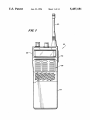
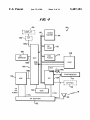
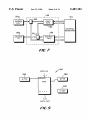
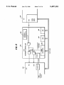
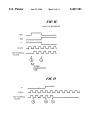
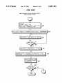
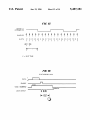
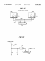
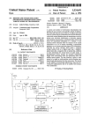
l| | |l l l l Il l l l l l l ltl l l gmlgl l l l l l l l l l l l l l l
United States Patent [191
[11]
Patent Number:
Bailey et al.
[45]
Date of Patent:
[54] LOW POWER ARCHITECTURE FOR
5,159,765 10/1992
5,170,490 12/1992
5,175,759 12/1992
5,241,537 8/1993
PORTABLE AND MOBILE TWO-WAY
RADIOS
[75] Inventors: Dissosway;
Timothy E. Russell
Dailey; L.
Marc
Croucher,
A.
all of
7/1994
Jan. 23, 1996
Critchlow ................................ .. 455/76
Cannon et al.
Metroka
.... .. . ... . .
Gulliford et al.
Sobti
5:327:55“)
5,487,181
. ,... .... ... .
Nickel et al. ..
. 455/343
. . . . . . ..
379/58
.. 370/1102
. . . ..
455/38.3
379/58
Vignali et a1. .......................... .. 455/15
Forest, Va.
FOREIGN PATENT DOCUMENTS
[73] Assignee: llilli'cicsiglrrilcilljiurltg/logge Communications
0034542 3/1980
Japan ................................... .. 455/343
OTHER PUBLICATIONS
Appl. No.: 969,739
“M-PD System . . . 136—174 MHz Personal Two-Way FM
Filed:
Radio Combination”; Maintenance Manual; GE Mobile
Oct. 28, 1992
Communications; LBI—31629A, May 1987.
Int. Cl.6 ...................... ...... .. H04B 1140; H04B 7/32
Hitachi H8/532 HD6475328, HD6435328
U.S. Cl. ............................ .. 455/89; 455/90; 455/343;
Manual (Jan. 1992).
Hardware
364/2286; 364/2302; 364/DIG. 1
Hitachi Single-Chip Microcomputer H8/330 HD6473308,
Field of Search .................................. .. 455/38.3, 343,
HD6433308 Hardware Manual-User’s Manual (Dec.
455/89-90, 73, 76, 183.2, 127; 379/58;
1989).
345/89, 148; 370/1102; 36402844538662,
Primary Examiner_chi H. Pham
Attorney, Agent, or Firm—Nixon & Vanderhye
References Cited
[56]
[57]
U.S. PATENT DOCUMENTS
4,384,361
4,437,095
4,562,307
ABSTRACT
An extremely compact, full featured portable radio archi
tecture conserves power by allowing a processor to sleep
except when it needs to perform tasks. A lower power
processor which acts principally as an interrupt controller
but which performs other functions as well (e.g., tone
5/1983 Masaki .................................... .. 455/31
3/1984 Akahori et al. .
12/1985 Bursztejn et al.
340/825.44
.... .. 379/61
4,598,258
7/1986
4,731,814
3/1988 Becker et al. ..
379/62
decode, synthesizer lock monitoring, etc.) so the main
4,830,832
4/1989 Nagata et al. ..
455/343
processor can sleep as much as possible and yet is assured
455/76
.... .. 455/76
of being awoken promptly when its processing power is
required. The resulting portable radio has extremely low
power consumption (e.g., on the order of 75 milliamperes
during trunked mode operation)—thereby permitting even a
4,870,699
4,887,311
12/1989
12/1989
Babano ..... ..
. 331/14
Garner ......... ..
Garner et al.
4,901,036
2/1990 Herold et al.
455/183 2
4,903,319
2/1990 Kasai et al.
. 455/33
4,947,454
8/1990 Garner
455/88
4,979,102 12/1990 Tokuume
364/200
relatively
small battery
pack to provide nearly 8 hours of
_
_
mmmumls 0Paramou The portable radio with battery is
5,001,776
455/343
small and lightweight enough to ?t into a front shirt pocket.
4,977,611
12/1990
3/1991
Maru .... ..
455/161
Clark .... ..
5,058,203 10/1991 Inagarm
5,109,537
455/89
35 Claims, 14 Drawing Sheets
4/1992 Toki ...................................... .. 455/343
‘r56
5?
l DISPIA‘7‘]
"1"‘ "3: $155 w,
120'\_\ TJP ‘l
L.
_J
1360:‘
:
2K
EEFHOM
RCP
136!)
mm
102\
1350
118
\
ASP
124
UDC
CTRL
RF SECTION
BK
1112
US. Patent
Jan. 23, 1996
Sheet 1 of 14
l 60
5,487,181
US. Patent
Jan. 23, 1996
Sheet 2 of 14
FIG 3
5,487,181
US. Patent
Jan. 23, 1996
Sheet 4 of 14
5,487,181
FIG 5
0000
8000
32K MASKED ROM
~14O
8K RAM
F800
F900
FA00
F800
F880
FF80
1 0000
FUTURE
RAM EXPANSION
VG DES CHIP
VG DSP CHIP
DUAL PORT RAM
ASIC
N108
1K RAM
INTERNAL REGlSTERS
spare
20000
spare
40000
64K FLASH EEPRQM
50000
80000
FUTURE
FLASH
EXPANSION
spare
L_______________i
~114
US. Patent
Jan. 23, 1996
Sheet 5 0f 14
5,487,181
=2 Om: Em NE
VI AI
“09
5Iwvm6n m v_vIAz<|1m IAvI
‘sSImAE9a2vo8EI
mm.\81in.
K62AI AEPI;
VA60I
WIv
SvE2I8m .
I.A652I8
I~
U Iv
wImAvaIg o(mM@IA0_.v8\I0
1IAI35
Iv
V.I VI
Ivwon.
Iv
mDQ< POwO NOwU mOmU .wO mOwO
US. Patent
Jan. 23, 1996
Sheet 6 of 14
5,487,181
1500
CONTROL
REGISTERS
1550b
FAR
FBR
FCR
\ /
DATA OUT
FIG 6’
US. Patent
Jan. 23, 1996
Sheet 8 of 14
5,487,181
FIG I0
WAKE UP SEQUENCE
NMI
_|'—L______
IRQ
____r———
IT
CLOCK
_.I_L_I_L__I_I__I_L_I_I_I"I.
RCP INTERNAL ___I_I_]"I_F'I_I"I_I_L
<5 <5
w
CLOCK
STABILIZATION
TIME
FIG II
IT
CLOCK
RCP INTERNAL
_____"—_|
MW
US. Patent
Jan. 23, 1996
Sheet 9 of 14
5,487,181
202
200
/ANY os\ YES
PROCESS
TASK
<TASKS READY
YE
<—'-S-<PEFIIPHERALS
‘RUNNING?
FIG I2
DETERMINE
SHORTEST TIME
TASK WILL WILL
BE AWAKED BY
PROCESS
INT THAT
WOKE CPU
208
US. Patent
Jan. 23, 1996
5,487,181
Sheet 10 of 14
SSBY SLEEP
ISSUE WAKEUP
CALL TO ICP
WITH MINIMUM
FIG I3
DISABLE INTS
AND SAVE
CPU STATES
220
224
CLEAR ASIC
TIMER,
SWITCH TO
NMI INT
226
CPU SSBY
SLEEP
228
UPDATE SYSTEM
TIMERS WITH
THE TIME THE
CPU WAS
ASLEEP
230
RESTORE CPU
STATES AND
ENABLE INTS
232
US. Patent
Jan. 23, 1996
Sheet 11 of 14
5,487,181
FIG I44
MRK CHANNEL GUARD DECODE
ENABLE TIMER CAPTURE
WITH BUFFERING AND DO
NOT ENABLE INPUT CAPTURE
300
FLAG (ICF) INTERRUPT
LAST-TIME = O
CURRENT_-SLOT = O
302
REMAINDER = O
SLOT = NUMBER OF FRT COUNTS
EQUAL TO TIME DETERMINED BY
1/8 CHANNEL GUARD PERIOD
RESET FRT
START F RT
304
US. Patent
Jan. 23, 1996
Sheet 12 of 14
5,487,181
FIG I45
MRK CHANNEL GUARD DECODE USING
FREE RUNNING TIMER
READ FRT
CURRENT__TIME = FRT
DELTA = CURRENT__TIIVIE — LAST___TIME
308
LAST__TIME = CURRENT__TII\/IE
NEW__SLOT = DELTA + CURRENT_SLOT * SLOT + REMAINDER
NEW__SLOT =
NEW_SLOT—8 * SLOT
NEW__SLOT =
NEW__SLOT + 8 * SLOT
CURRENT_SLOT = QUOTENT OF NEW__SLOT / SLOT
REMAINDER = THE REMAINDER OF NEW__SLOT / SLOT
PASS CURRENT_SLOT
TO CHANNEL GUARD 32o
310
318
US. Patent
Jan.23, 1996
Sheet 13 of 14
5,487,181
FIG I5
LIMITEDXX
FILTEREDCG
SAMPLESTTTTTHTTTHTHTT
SLOTS l1|2l3|4!5|e|7ls‘1lzlsl4ls‘el7lsl
wk
'<—_T—>|
X
SLOT TIME
FIG I6
SYNTHESIZER LOCK
DATA
ENABLE
WIDE
WIDE /
NARROW A
NARROW
LOCK DETECT
|<_ TIME
LOCK
US. Patent
Jan. 23, 1996
Sheet 14 of 14
5,487,181
FIG I7
SHARED SERIAL PORTS
102
104
RX
TX
RX
TX
354
§
356)
RX
TX
124
FIG I5’
BOARD TYPE
5V
gm /
‘130
132
--->
REGISTER
S/W
5,487,181
1
2
LOW POWER ARCHITECTURE FOR
PORTABLE AND MOBILE TWO-WAY
RADIOS
power more powerful lamp for the same amount of time).
However, the larger “D” cells are also several times more
bulky and heavy as comparedto penlight cells. If the amount
of current continually being drawn by a radio from the
battery can be decreased, then the radio can operate for a
FIELD OF THE INVENTION
longer time on a single battery charge. Moreover, very low
The invention relates to improvements to radio transceiv~
ers, and more particularly, to features for reducing the power
consumption of a portable and/or mobile two-way radio.
BACKGROUND AND SUMMARY OF THE
INVENTION
current consumption means that even a relatively small
battery can be used to provide relatively long periods of
operation.
10
Unfortunately, the sophisticated features provided on
today’s two-way radios require large amounts of software.
This software can best be developed and maintained using
high level languages such as C. However, these languages
require high performance microcontrollers for proper execu
Most people have at least seen, if not actually used, a
hand-held (“walkie'talkie”) portable two-way radio. Hand
held radios have revolutionized the way some people work.
For example, a police officer can bring a handheld radio
tion speed. These controllers require a great deal of current.
when investigating on foot——thereby increasing safety and
microcontrollers, but such constructions prevent the use of
Some past designs have used multiple low performance
high level languages and their advantages in development
time and maintainability. Other designs have used a single
effectiveness due to the ability to instantaneously commu
nicate with a dispatcher or other police o?icers. Fire and
low power rnicrocontroller with custom hardware. This
solution su?fers from the same problems as multiple low
performance controller technique, and also is not very
?exible since the functions of the custom hardware become
?xed once the custom hardware design is ?nalized. Other
Smaller is generally better when it comes to hand-held
25 prior art designs may use the “sleep mode” of a processor to
radios. Smaller radios are more convenient to carry, reduce
turn off the CPU, but may keep the peripherals running.
user fatigue, and may be able to go places that larger radios
The present invention, in contrast, provides a miniaturized
cannot go. For example, undercover police officers are not
two-way radio design providing the performance offered by
able to carry large two-way radios since such radios could be
a high power CPU while also providing low current con—
easily seen and thus “tip off” criminals and others under
sumption. This low current consumption permits even a very
investigation. A radio small enough to ?t into the officer’s
small battery pack to power the radio for an entire (approxi
front shirt pocket could be concealed underneath a normal
rescue workers, paramedics, power and telephone company
?eld technicians, and other people performing tasks critical
to general safety and welfare greatly bene?t from hand-held
two-way radios.
mately 8 hour) shift. As a result, the radio with battery
jacket and thus could actually be carried by the police officer
during covert and undercover operations. The ability of a
connected is light, lean and super compact. The preferred
Recent innovations in custom chip design allow radio
embodiment radio is the ideal portable for covert operations
and any other applications where concealed and/or
extremely miniaturized radios are required. For example, the
preferred embodiment weighs less than 20 ounces (including
battery), is slightly more than 1 inch deep, and is slender and
lightweight enough to slip into a front shirt pocket.
designers to eliminate circuits, reduce the number of com
ponents and cut power drain. Thus, it is now possible to
provide a full-featured digital radio transceiver in a very
embodiment of the invention include:
Distribution of radio functions between a high-power}
police o?icer to carry such a two-way radio while under
cover would greatly increase the o?icer’s safety and under
cover operations. However, various problems have in the
past prevented such a compact full-featured radio from
being widely produced.
Features provided by the presently preferred exemplary
small, low pro?le package. However, battery miniaturiza
tion has not kept up with advances in semiconductor min 45
iaturization. Whereas only a few years ago the size and
weight of the battery constituted only a small percentage of
the overall size and weight of a hand-held radio, the battery
may now comprise a signi?cant percentage (on the order of
half) of the radio’s size and weight.
Hand-held radios have long been powered by removable
rechargeable battery packs that attach to the lower portion of
the radio housing so as to become part of the radio hand grip.
Such detachable reusable battery packs allow users to easily
swap a recharged battery for a “dead” battery pack. The
“dead” pack may then be recharged without removing the
radio from service during the recharge procedure. Once
cessor can be placed into a “software stand by” mode
much of the time (i.e., except when actually needed);
50
A current saving architecture for a radio using software
standby (“SSB”) mode with ASIC support to switch
from IRQ (maskable) to NMI (non-maskable) interrupt
inputs;
Main CPU reads watchdog timer to accurately maintain
system (real) time despite intermittent lapses into the
55
charged, a battery pack should last at least as long as a
typical work shift (e.g., eight hours) so that the radio user
does not need to carry additional battery packs and/or swap
batteries in the middle of a shift.
As everyone who has ever bought a ?ashlight knows,
larger batteries deliver more current and thus have a longer
life (assuming constant current draw). For example, a size
“D” ?ashlight cell delivers several times the amount of 65
current delivered by a much smaller “AA” penlight ?ash
light cell, and may thus power a lamp for a longer time (or
high-capability processor, a low-power/low-capability
processor, and additional logic (e.g., an application
speci?c integrated circuit) so that the high-power pro~
sleep mode;
A free running timer performs channel guard decode thus
allowing simultaneous decode of channel guard and
T99 signalling using the single low power processor;
FIFO (?rst in ?rst out) data buffer so that the high-power
processor can sleep;
Pulse width modulator is used to control the backlight
brightness of the LCD display and thus save current;
Low power processor decodes “low speed” digital sig
nalling so high-power processor can sleep;
Low power processor monitors synthesizer lock line to
allow high-power processor to sleep;
5,487,181
4
3
SSB is integrated into the high power processor operating
system;
Serial port is shared between micro-controllers to provide
great ?exibility in design and current savings (i.e.,
allowing the low-power processor to handle serial
messages while allowing the high-power processor to
sleep); and
Board type resistors identify the type of board.
DETAILED DESCRIPTION OF THE
PRESENTLY PREFERRED EXEMPLARY
EMBODIMENT
5
FIG. 1 is a front elevated view of a presently preferred
exemplary embodiment of a two-way portable hand-held
radio transceiver (“radio”) 50 provided by the present inven
tion. Radio 50 includes a main unit 52 and a detachable
battery pack 54. Main unit 52 includes all of the electronics
10
BRIEF DESCRIPTION OF THE DRAWINGS
(both digital control and radio frequency) required for
two-way RF communications. Battery pack 54 is detachable
and houses one or more rechargeable (e.g., NICAD) batter
These and other features and advantages of the present
invention will be better and more completely understood by
referring to the following detailed description of a presently
preferred exemplary embodiment in connection with the
ies that provide power for operating main unit 52. In the
preferred embodiment, the battery pack may be provided in
three different sizes for three different power lifetimes.
Preferred embodiment radio 50 is lightweight and slender.
The following are exemplary dimension and weight speci
?cations for main unit 52 and battery pack 54.
drawings, of which:
FIG. 1 is an elevated front view of a presently preferred
exemplary embodiment of a portable two-way radio trans
ceiver provided by the present invention;
20
FIG. 2 is an elevated side view showing the FIG. 1 radio
and, for size comparison purposes, a pair of conventional
Less Battery, Knobs and Antenna
sunglasses;
FIG. 3 is an elevated perspective view of the FIG. 1 radio
resting within a user’s front shirt pocket;
FIG. 4 is a high level block diagram of an exemplary
architecture of electronics within the FIG. 1 radio;
FIG. 5 is a schematic diagram of an exemplary address
space for the “RCP” processor shown in FIG. 4;
FIG. 6 is an exemplary block diagram of the ASIC shown
in FIG. 4;
FIG. 7 is a schematic diagram of an exemplary modem,
buffer and control register architecture of the FIG. 6 ASIC;
FIG. 8 is a conceptual schematic diagram showing exem
M-RK II (Display + keypad)
With High Capacity Battery
M-RK II:
7'' X 2.7" X 1.16"
176.8 x 68 mm x
40.6 mm
M-RK I:
7'' X 2.7“ X 1.18“
176.8 X 68 mm x
30 mm
35
WEIGHT
M-RK II (Less Battery):
M-RK I (Less Battery):
10 oz (258 g)
8.8 oz (250 g)
BATTERIES
CAPACITY
processor;
Medium
45
being “awakened” by the ASIC;
FIGS. 14A-14B together are schematic ?owcharts of
the FIG. 4 ICP processor;
4" X 2.7" X 1.18"
101 mm x 68 mm X
30 mm
FIGS. 10—11 are timing diagrams showing exemplary
wake-up and sleep sequences, respectively, of the RCP
exemplary channel guard detection technique performed by
101 mm X 68 mm X
40.6 mm
M~RK I (No Display + keypad)
FIG. 9 is a detailed block and schematic diagram showing
exemplary interrupt control structure for the FIG. 4 ASIC;
exemplary program control steps performed by the FIG. 4
low-power ICP processor in order to provide channel guard
decode using a free running timer;
FIG. 15 is an exemplary timing diagram showing the
4“ x 2.7" x 1.6“
25
plary operation of the buffer shown in FIG. 7;
FIG. 12 is a schematic ?owchart of exemplary operating
system control steps performed by the RCP processor shown
in FIG. 4;
FIG. 13 is a schematic ?owchart of exemplary program
control steps performed by the FIG. 4 RCP processor upon
7.5 VDC (nominal)
INPUT VOLTAGE:
DIMENSIONS (Typical) H X W X D
50
DIMENSION (H x W X D)
WEIGHT
2.54" x 2.7" X 1.1"
6.4 oz.
64.6mmx68mmx28mm
163g
High
3.1“ X 2.7" X 1.1"
10.4 oz.
79.6mmx68mmx28mm
296g
Extra High:
3.8“ X 2.9" X 1.1"
TBD
The radio shown in FIG. 1 includes an LCD display and
a keypad 58. However, as indicated in the dimension/weight
speci?cation set forth above, in another embodiment the
display 56 and keypad 58 may be omitted (with several light
emitting diode indicators being used in lieu of the display)
so as to provide an even smaller: depth and reduced weight.
55
FIG. 16 is an exemplary timing diagram showing the
synthesizer lock detect performed by the low-power ICP
processor shown in FIG. 4;
FIG. 17 is a high level block diagram showing an exem
Without display 56 and keypad 58, radio 50 is so slim that
it may easily be inserted into a front shirt pocket (see FIG.
3). Even with the display and keypad, the radio 50 is
extremely slim and trim (see the side view of FIG. 2).
The following is a list of a few of the salient advantageous
features of the radio 50 shown in FIG. 1:
plary serial port sharing arrangement between the high
power and low-power processors RCP and ICP shown in
FIG. 4; and
FIG. 18 is a schematic and block diagram showing an
exemplary preferred technique provided by the preferred
embodiment of the present invention for detecting board
type.
65
PRODUCT FEATURES
MAI OR BENEFITS
Small size and
light weight
Easy to carry, easy to conceal and
easy to use.
Top mounted rotary
Convenient Eyes Free operation
controls
while worn on the belt.
5,487,181
PRODUCT FEATURES
5
6
-continued
interaction with RCP 102 and ICP 104 will be described in
more detail shortly.
Main unit 52 further includes an optional display proces
sor 120 connected to LCD display 56. Display processor 120
MAJOR BENEFITS
Two line dot matrix
Clear display of system and group
LCD (M-RK 11)
information. Ideal for
in the preferred embodiment comprises an intelligent LCD
display controller of conventional design including a four
bit micro-controller and integral LCD driver. This approach
Alphanumerics. Characters invert
180° for easy-to-read viewing while
worn on the belt.
System keypad
Provides access to system and radio
(M—RK II)
features like individual calls,
off loads many of the tedious display functions from RCP
102—allowing the RCP to sleep more. Display 56 in the
preferred embodiment comprises two rows of eight charac
ters using dot matrix characters.
scan, and menu select. Backlit for
night viewing.
Remote radio disable
Allows dispatcher to “Kill” an
EDACS radio in the event it is
reported lost or stolen.
Emergency button
lrnmediate signalling of emergency
condition including user ID to
15
alert dispatch center and group
users.
EDACS signalling
Conventional
signalling
Includes all the bene?ts of EGE’s
EDACS fault tolerant
communication.
Includes GE STAR ID/Emer—
gency and TYPE 99 decoding
for conventional radio ID and
signals over the air via antenna 60. RF section 122 receives
and detects RF signals at frequencies selected by synthesizer
117 and provides the detected audio to ASP 118 for ?ltering
and further processing. A conventional microphone, loud
individual calling.
FIG. 4 is a schematic diagram of an exemplary architec
ture of radio main unit 52 shown in FIG. 1. Main unit 52
speaker and associated ampli?cation circuitry (not shown) is
25
includes a high-powered radio control processor (“RCP”)
102; a lower-power interrupt control processor (“ICP”) 104;
and a custom application speci?c integrated circuit
(“ASIC”) 108. RCP 102, ICP 104 and ASIC 108 commu
nicate with one another via a general-purpose conventional
example, frequencies of operation, radio identi?cation,
access memory 112, ?ash memory 114, and a digital voice
group and individual IDs, and the like.
guard block 116, all of conventional design. Voice guard
module 116 provides encrypted voice communications. This
module is of conventional design and communicates with
used to convert user’s speech into audio signals and to
convert received audio into sound for listening by the user.
A universal device connector (“UDC”) 124 provides a
digital serial port for coupling with the outside world. UDS
124 may be used, for example, to load new “personality”
programming into the radio 50 from an external program
ming source. Such “personality” de?ning data speci?es, for
address/data bus 110. Also connected to bus 110 are random
RCP 102 via the address/data bus 110.
RF section 122 performs all of the radio frequency signal
processing within main unit 52. RF section 122, for
example, modulates a radio frequency signal (generated at a
frequency controlled by a conventional frequency synthe
sizer 117 under the control of ICP 104) with audio received
from ASP 118 (or digitized audio received from voice guard
block 116). RP section 122 transmits such modulated RF
35
'
ICP 104
ICP 104 in the preferred embodiment is a masked H8/33O
RCP 102 in the preferred embodiment comprises a Hita
chi H8/532 micro-controller. RCP 102 is the high perfor
mance CPU coordinating all of the functions of main unit
52. ICP 104 in the preferred, embodiment is a Hitachi
high performance single chip micro-computer providing
16K bytes of on chip ROM, 512 bytes of on chip RAM, 15
bytes of dual port RAM (for master/slave interface), serial
I/O, general purpose I/O ports, and A/D converter and
internal timers. The main function of ICP 104 is to handle
user interface interrupts and tone decodes so that RCP 102
H8/330 single chip micro-computer which acts as a smart
interrupt controller for RCP 102. More information regard
ing these conventional Hitachi processors may be found in
can remain in a low power state as much as possible. ICP
various publicly available printed publications, including the
104 is thus treated more as an intelligent interrupt controller
than as another independent CPU within the architecture of
Hitachi
Single~chip
Microcomputer
H8/330,
radio main unit 52. The functions performed by ICP 104 can
HD6473308, HD66433308 Hardware Manual, ADE-602
be well de?ned and speci?ed by internal masked ROM
O26(0), published (1st Edition) December 1989 (Hitachi
programming. The interface and operation of ICP 104 is as
Corp); and
generic as possible to allow this component to support the
50
different requirements of a mobile radio and a portable radio;
Hitachi H8/532, HD6475328, HD6435328 Hardware
following:
45
Manual, M2lT0O2, published January 1992 (Hitachi Corp.)
processor (ASP) 118 of conventional design that handles
and to support minor design changes without re-masking.
Therefore, ICP 104 is programmed as a con?gurable I/O
device that can perform tone decode, keypad and U0
generated, for example.
decodes, sub-audible tone encodes, low speed data decode,
Main unit 52 further includes a custom audio signal
most of the audio ?ltering for the radio. ASP 118 may be a 55 manipulation. ICP 104 is preferably con?gured by RCP 102
at time of power up of radio main unit 52.
single chip device that is capable of powering down unused
circuitry while continuing to generate alert tones. This
The primary functions of the ICP are: key-pad scan,
allows RCP 102 to sleep while the alert tones are being
discrete I/O monitoring, display backlight control, tone‘
ICP 104 handles the user interfaces, performs tone decod 60 carrier detection/squelch control, RSSI monitoring, and syn
thesizer control.
ing, and controls radio frequency synthesizer 116 in the
preferred embodiment. ASIC 108 contains circuitry which
In connection with keypad scan, ICP 104 scans the keypad
handles the transmission and reception of digital information
58 in a conventional manner to detect user depression of
over the air. ASIC 108 further includes interrupt control
keys, and also monitors group knob and volume knob
settings (see FIG. 1). If a key is depressed (or a knob is
turned), ICP 104 noti?es the RCP 102 via a dual port RAM
message.
circuitry, clock control circuitry and address decode logic.
ASIC 108 is in some sense the “glue that holds everything
together” in the preferred embodiment. ASIC 108 and its
65
5,487,181
7
8
The discrete I/O monitoring performed by ICP 104
includes monitoring the emergency and push-to-talk
(“PTI‘”) buttons (not shown). These I/O signals are checked
embodiment: MRK-I=ground, MRK-II=Vcc, and Delta
2:Vcc/2. Other voltage levels intermediate to Vcc and
ground potential may be used to specify other board types if
each time the keypad 50 is scanned. ICP 104 noti?es RCP
102 if one of the buttons is depressed. ICP 104 also monitors
its UART for data from UDC 124.
With regard to backlight control, ICP 104 includes an
internal pulse width modulator timer module with two
independent channels that are functionally identical. Each
PWF channel generates a rectangular output pulse with a
desired. FIG. 18 shows an exemplary resistive divider
arrangement 130 that may be used to supply the analog
voltage indicating board type. The V 2 output of divider 130
is coupled to an internal A/D converter 132 within ICP 104
(or RCP 102). The output of the A/D converter is read into
a register 134 (also internal to the ICP or RCP), from which
the register contents can be read by software. The software
may branch or otherwise perform different functions
depending on the register contents. This capability of ICP
duty factor that is programmable from 0 to 100%. The duty
factor is speci?ed in an 8-bit duty register (DTR). See page
171 et seq. of the above-referenced H8/330 Hardware
104 (RCP 102) to automatically detect and adapt to the type
Manual. In the preferred embodiment, this pulse width
of board or product in which it is installed allows a single
“masked” processor to be used in a variety of diiferent
modulator timer is used to control the brightness of a
backlight 56a provided behind display 56. As is well known,
LCD displays do not (unlike LED components) generate
light but rather must rely on ambient lighting and/0r back
products without requiring changes to the mask.
lighting for readability. The preferred embodiment provides
a backlight behind display 56 which may be activated by
RCP 102 each time the user depresses a key of keypad 58.
In the preferred embodiment, ICP 104 drives this backlight
using one of its PWM outputs. The duty cycle of the PWM
output thus controls the brightness of backlighting. The
RCP 102
20
voice guard block 116, ICP 104, and IASIC 108 via data bus
110 (see FIG. 5, which schematically illustrates the address
space of the RCP). In addition, RCP 102 has access to the
backlight level is speci?ed by RCP 102 in the preferred
embodiment. Using the pulse width modulator allows the
ASP 118, EPROM 126 and display processor 120 via serial
links 136A—136C.
As mentioned above, RCP 102 in the preferred embodi
intensity of the backlight to be varied by the user to select
the lowest usable intensity to save power.
With regard to tone encode and decode, ICP is capable of
coding both channel guard and so called “T99” signalling
simultaneously. Brie?y, T99 decoding is performed in a
conventional manner, while channel guard decoding is per
formed using an internal timer capture register. Further
details regarding the channel guard decoding will be pro
vided shortly. ICP 104 also performs channel guard and
digital channel guard tone encoding using its two Walsh bits.
This eliminates the potential risk that RCP 102 may not be
able to successfully perform both DTMF and channel guard
tone encoding simultaneously. With regard to low speed data
decode, ICP 104 decodes EDACS conventional low speed
data messages (which are substantially continually transmit
ted subaudibly over assigned channels). ICP 104 does not try
RCP 102 is the main processor for radio main unit 52.
RCP 102 has access to the RAM 112, ?ash memory 114,
ment is a Hitachi H8/532 microcomputer which runs at
approximately 9.8304 megahertz or at some other value in
multiple increments of 2.4576 megahertz (these frequencies
were selected because they support the accurate generation
of 38.4K baud data). It is preferable to use the slowest
possible clock frequency because this reduces power con
sumption and spurs.
35
The Hitachi H8/532 has the following features which are
advantageously used in the preferred embodiment of the
present invention:
16-bit internal architecture
8 l6-bit general purpose registers
32K bytes mask ROM
1K RAM
10-Bit A/D converter
to determine the contents of the message, but instead simply
passes each valid message to RCP 102 for processing. This
allows the RCP 102 to sleep more often while nevertheless
permitting the higher capability RCP to perform content
Full duplex UART
3 l6-bit timers
determinations.
With regard to carrier detection and squelch control, ICP
104 performs these functions as part of its standard tone
Watchdog timer
18-bit timer
decode operations. ICP 104 in the preferred embodiment
also supplies canier (i.e., squelch) information to RCP 102
3 pulse width timers
to allow so-called “feature” tone decodes. RCP 102 is able
Interrupt controller
Current saving modes:
Sleep mode
DMA
to tailor the responsiveness (slow/fast) of the squelch attack
provided by ICP 104 (e.g., by writing parameters to the
ICP). ICP 104 also is responsible for loading (programming)
55
synthesizer 117 and monitoring the lock status of the syn
thesizer (as will be explained in greater detail shortly).
In the preferred embodiment, ICP 104 also determines,
based upon an analog voltage value applied thereto, the type
Reduces current drain 30%.
Software Standby Mode (SSB)
Pulls nano amps.
Turns oif CPU and peripherals.
Maintains outputs but registers of onboard support
of board or product in which the ICP is installed. Such
determination may also be performed by RCP 102. This
board type determination allows the ICP 104 (RCP 102)
modules are reset to initial values.
Maintains internal RAM/registers.
software to adjust automatically to different hardware con
?gurations. In the preferred embodiment, the analog input
signal is generated by a resistor divider network between
Vcc and ground. The following exemplary board types have
been de?ned with regard to ICP 104 in the preferred
CPU sleeps, but peripherals continue to work.
Wakes up from peripheral interrupts.
Wakes up in 52 micro seconds from non-maskable
65
interrupt.
RCP 102 and ICP 104 communicate with one another via
a dual port RAM within ICP 104. The protocol for the data
5,487,181
9
10
exchange is de?ned in the H8l330 hardware manual. This
on-chip dual port RAM is provided to permit access by both
the CPU in the H8/330 chip and by a master CPU on another
program and personality must be uploaded (e.g., from a
personal computer program of conventional design via uni
versal device connector 124). The new personality is added
chip.
The memory organization of main unit 52 will now be
described in connection with FIGS. 4 and 5. Main unit in the
preferred embodiment has a total of 9K of RAM—lK
onboard RCP 102 and 8K on a RAM 112 connected via bus
110. This collection of RAM locations is available for
variables, buffers, etc. RAM 112 is not battery backed up.
RCP 102 has 32K of masked ROM 140 onboard. Using
this masked ROM 140 saves current by eliminating the
to the code and is downloaded into main unit 52.
EPROM 126 is accessible via a IIC link 136B connected
to RCP 102. EPROM 126 contains user con?gurable con
tents that must be maintained throughout a power cycle.
These parameters include, for example, volume, current
group/system, stored phone numbers, etc.
10
ASIC 108
power consumed by reading ?ash memory 114. Masked
ROM 140 contains the following program elements
(selected because they are stable, independent and easy to
ASIC 108 is basically a “glue chip” that integrates many
miscellaneous functions. ASIC 108 provides the following
test);
Data transmission and reception using programmable
sync character (i.e., barker)
features:
BIOS—Basic Input/Output System. All the routines that
interface directly to the hardware. This provides a layer
Sync character can have up to 4 bit errors
of hardware independence. The application program
calls BIOS routines to implement hardware dependent
This allows the ASIC to get synchronized with the
received data while the RCP sleeps
64 byte transmit/receive buffer
functions. If the hardware changes, only the BIOS need
change. The application does not know the difference.
This allows the ASIC to receive or transmit data while the
The BIOS includes the bootstrap loader to load new
program code in the ?ash.
Operating System-(event driven multi-tasking)
25
Routines that run continuously (this eliminates calls to
?ash memory and reduces current drain).
Routines that require fast execution.
Since the BIOS is masked, the preferred embodiment of
RCP sleeps.
Limited full duplex operation.
Watchdog timer
This timer can be read by the RCP 102. The RCP 102 uses
this timer to keep track of how long it was asleep so that it
can update its own timers which are turned off in software
standby mode.
the present invention provides a way to recover from many
Interrupt control circuitry
bugs that might crop up. This is done by using a BIOS vector
table. The table contains a starting vector for each of the
BIOS routines. The BIOS installs its vector table in RAM
(e.g., internal RAM or external RAM 112) at power up. The
This supports interrupts related to data transmission and
reception and also ties the RCP 102 and ICP 104 together to
allow the RCP to sleep.
Clock control circuitry
This circuitry divides the single system clock down so
that the lowest possible clock rates are used by each device.
applications program can overwrite the vector table to install 35
a di?erent BIOS routine. This allows bad routines to be
replaced by new routines stored in ?ash memory 114.
Address decode
Interrupt routines are handled in a similar way in the
FIG. 6 is a block diagram of an exemplary architecture for
preferred embodiment. Interrupt vectors are stored in
ASIC 108 shown in FIG. 4. The primary purpose of ASIC
masked ROM 140. Interrupts jump through a RAM vector 40 108 is to off-load tasks from RCP 102 so that the RCP can
to the actual internlpt routine. Information stored in ?ash
spend as much time as possible in the low power state. This
memory 114 has the capability of installing or replacing
these interrupt routines.
greatly reduces the current requirements of radio main unit
Main unit 52 has, as mentioned above, 64K of ?ash
EPROM 114 available (additional address lines on bus 110
are available for expansion to 256K if space and cost allow).
Flash memory 114 is an EEPROM that must be erased in
large blocks rather than a byte at a time. The use of ?ash
memory 114 allows an entire program to be changed without
integrated circuit”) for device 108 reduces printed circuit
board space required and also reduces parts count.
opening main unit 52, but single values (like current vol
ume) cannot be changed individually. In the preferred
embodiment, ?ash memory 114 contains the application
52. In addition, the use of an ASIC (“application speci?c
As shown in FIG. 6, ASIC 108 includes a modem 150, a
bidirectional ?rst-in-?rst-out (FIFO) buffer 152, a control
register bank 154, an interrupt controller 156, a watchdog
timer 158, an address decoder 160, and a clock controller
50
register bank 154 contains control and status registers, and
program. This is the high level code that provides the user
interface and otherwise de?nes the features and operations
provided by radio main unit 52. In the preferred embodi
ment, this application program is written in the C language
and is compiled for execution on the H8/532.
In the preferred embodiment, the ?ash memory 114 also
contains a large part of the personality de?ning information
described above. Flash memory 114 is not large enough to
hold the entire personality de?ning data in the preferred
embodiment. Therefore, any part of the personality de?ning
162. Modern 150 is of conventional design, and permits
digital data to be sent and received over the RF link. Control
is the interface point for RCP 102. RCP 102 can write to
55
and/or read from registers within control register bank 154
via address bus 110.
The following is an exemplary de?nition of control reg
isters within ASIC control register bank 154:
Read/
Name
MDCRl
MDCR2
PMRl
stored in the ?ash memory 114. The remaining personality
de?ning data is stored in EPROM 126 where it can be easily 65 PMR2
MACR
changed. This means that any time the personality data
MRCR
data that cannot be changed by the user or over the air is
stored in the ?ash memory 114 needs to be changed, the
Write
Description
W
W
W
W
R/W
Modem Divide Control Register (low)
Modem Divide Control Register (high)
Pattern Match Register (low)
Pattern Match Register (high)
Match Control Register
R/W
Modem Receive Control Register