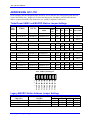
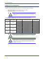
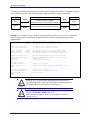
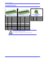
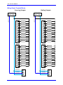
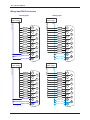
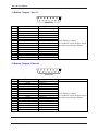
1
^1 USER MANUAL ^2 Accessory 11E ^3 24 Opto In/24 Opto Out ^4 3AX-603307-XUXX ^5 December 17, 2012 Single Source Machine Control Power // Flexibility // Ease of Use 21314 Lassen Street Chatsworth, CA 91311 // Tel. (818) 998-2095 Fax. (818) 998-7807 // www.deltatau.com ACC-11E User Manual Copyright Information © 2011 Delta Tau Data Systems, Inc. All rights reserved. This document is furnished for the customers of Delta Tau Data Systems, Inc. Other uses are unauthorized without written permission of Delta Tau Data Systems, Inc. Information contained in this manual may be updated from time-to-time due to product improvements, etc., and may not conform in every respect to former issues. To report errors or inconsistencies, call or email: Delta Tau Data Systems, Inc. Technical Support Phone: (818) 717-5656 Fax: (818) 998-7807 Email: [email protected] Website: http://www.deltatau.com Operating Conditions All Delta Tau Data Systems, Inc. motion controller products, accessories, and amplifiers contain static sensitive components that can be damaged by incorrect handling. When installing or handling Delta Tau Data Systems, Inc. products, avoid contact with highly insulated materials. Only qualified personnel should be allowed to handle this equipment. In the case of industrial applications, we expect our products to be protected from hazardous or conductive materials and/or environments that could cause harm to the controller by damaging components or causing electrical shorts. When our products are used in an industrial environment, install them into an industrial electrical cabinet or industrial PC to protect them from excessive or corrosive moisture, abnormal ambient temperatures, and conductive materials. If Delta Tau Data Systems, Inc. products are directly exposed to hazardous or conductive materials and/or environments, we cannot guarantee their operation. A Warning identifies hazards that could result in personal injury or death. It precedes the discussion of interest. WARNING A Caution identifies hazards that could result in equipment damage. It precedes the discussion of interest. Caution A Note identifies information critical to the user’s understanding or use of the equipment. It follows the discussion of interest. Note ACC-11E User Manual MANUAL REVISION HISTORY REV. 1 2 3 4 5 DESCRIPTION ADDED CE DECLARATION REVS. TO J1& J2, PINS 8 & 15, P. 31 REVS. TO ELEC. SPECS, P. 3 ADDED UL SEAL TO MANUAL COVER UPDATED AGENCY APPROVAL/SAFETY SECTION REFURBISHED ENTIRE MANUAL DATE 06/07/06 05/11/07 07/27/07 CHG. CP CP CP APPVD SF AO BP 10/01/09 CP SF 12/17/12 GS R.N ACC-11E User Manual Declaration of Conformity Application of Council Directive: 89/336/EEC, 72/23/EEC Manufacturers Name: Delta Tau Data Systems, Inc. Manufacturers Address: 21314 Lassen Street Chatsworth, CA 91311 USA We, Delta Tau Data Systems, Inc. hereby declare that the product Product Name: Accessory 11E Model Number: 603307 And all of its options conforms to the following standards: EN61326: 1997 Electrical equipment for measurement, control, and laboratory useEMC requirements EN55011: 1998 Limits and methods of measurements of radio disturbance characteristics of information technology equipment EN61010-1 Electrical equipment for measurement, control, and laboratory useSafety requirements EN61000-3-2 :1995 Limits for harmonic current emissions. Criteria A A14:1998 EN61000-3-3: 1995 Limitation of voltage fluctuations an d flicker in low-voltage supply systems for equipment with rated current 16A. Criteria B. EN61000-4-2:1995 Electro Static Discharge immunity test. Criteria B A1: 1998 EN61000-4-3: 1995 Radiated, radio-frequency, electromagnetic field immunity test. A1: 1998 Criteria A EN61000-4-4: 1995 EN61000-4-5: 1995 Electrical fast transients/burst immunity test. Criteria B EN61000-4-6: 1996 Surge Test. Criteria B EN61000-4-11: 1994 Conducted immunity test. Criteria A Voltage dips test. Criteria B and C Date Issued: 11 May 2006 Place Issued: Chatsworth, California USA Yolande Cano Quality Assurance Manager Mark of Compliance ACC-11E User Manual Table of Contents INTRODUCTION .....................................................................................................................6 SPECIFICATIONS ...................................................................................................................7 Environmental Specifications ......................................................................................................7 Electrical Specifications ..............................................................................................................7 Physical Specifications ................................................................................................................7 Agency Approval and Safety .......................................................................................................8 ADDRESSING ACC-11E .........................................................................................................9 Turbo/Power UMAC and MACRO Station Jumper Settings........................................................9 Legacy MACRO Station Address Jumper Settings ......................................................................9 Sinking or Sourcing Output Select ............................................................................................ 10 I/O Gate Data Clock Select ....................................................................................................... 10 Hardware Address Limitations .................................................................................................. 11 USING ACC-11E WITH TURBO UMAC ............................................................................. 13 Configuring the Control Word................................................................................................... 13 Accessing I/O data points (M-Variables) ................................................................................... 14 USING ACC-11E WITH POWER UMAC SCRIPT PROGRAMING ................................ 16 Configuring the Control Word................................................................................................... 16 Accessing I/O Data Points (Pointers) ......................................................................................... 17 Suggested M-Variables ......................................................................................................... 17 USING ACC-11E WITH POWER UMAC C PROGRAMING ............................................ 18 Setting Up Digital I/O Access ................................................................................................... 18 Function for Setting the Control Word: ACC11E_SetControlWord() .................................... 18 Function for Reading the State of Inputs: ACC11E_GetInputState() ..................................... 19 Function for Reading the State of Outputs: ACC11E_GetOutputState() ................................ 19 Function for Writing to Outputs: ACC11E_SetOutputState() ................................................ 20 Header and Source File ........................................................................................................ 22 User Written Functions......................................................................................................... 26 Setting Up the Control Word ..................................................................................................... 28 USING ACC-11E WITH UMAC MACRO STATION ......................................................... 30 Quick Review: Nodes and Addressing....................................................................................... 30 Setting Up The Control Word.................................................................................................... 33 Transferring Data Points over I/O Nodes ................................................................................... 35 Preparing for I/O Data Transfer on the MACRO16 Station .................................................. 36 MS{anynode},MI71: 24-Bit Transfer .................................................................................... 37 Table of Contents 4 ACC-11E User Manual MS{anynode},MI69 and MI70: 16-Bit Transfer .................................................................... 42 MS{anynode}, MI171, MI172, and MI173: 24-Bit/16-Bit Transfer........................................ 46 LAYOUTS & PINOUTS ......................................................................................................... 47 Board Layout Diagrams ............................................................................................................ 47 Wiring Considerations............................................................................................................... 48 Terminal Block Option.............................................................................................................. 49 TB1 Top: Inputs 1 thru 12..................................................................................................... 49 TB2 Top: Inputs 13 thru 24................................................................................................... 49 TB3 Top: Reference Voltages ............................................................................................... 49 Wiring Input Terminal Blocks ............................................................................................... 50 TB1 Bottom: Outputs 1 thru 12 ............................................................................................. 51 TB2 Bottom: Outputs 13 thru 24 ........................................................................................... 51 TB3 Bottom: Reference Voltages .......................................................................................... 51 Wiring Output Terminal Blocks ............................................................................................ 52 D-Sub Option ............................................................................................................................ 53 J1 Top: Inputs 1 thru 12 ....................................................................................................... 53 J2 Top: Inputs 13 thru 24 ..................................................................................................... 53 Wiring Input DB15 Connectors ............................................................................................ 54 J1 Bottom: Outputs 1 thru 12 ................................................................................................ 55 J2 Bottom: Outputs 13 thru 24 .............................................................................................. 55 Wiring Output DB15 Connectors .......................................................................................... 56 SCHEMATICS........................................................................................................................ 58 APPENDIX A: USING THE UMAC CONFIG PRO2 TOOL .............................................. 60 APPENDIX B: FULL TURBO UMAC M-VARIABLE MAPPINGS .................................. 66 APPENDIX C: FULL POWER UMAC M-VARIABLE MAPPINGS ................................. 78 APPENDIX D: THE CONTROL WORD .............................................................................. 90 Table of Contents 5 ACC-11E User Manual INTRODUCTION The ACC-11E is a 24 In/24 Out general purpose I/O card. Built in the 3U euro card format, it can be used in the following products: - Turbo UMAC Power UMAC UMAC MACRO Station All inputs and outputs are 12-24 VDC, optically isolated, and can be configured as sinking or sourcing. Introduction 6 ACC-11E User Manual SPECIFICATIONS Environmental Specifications Description Operating Temperature Storage Temperature Humidity Specification 0°C to 45°C, -25°C to 70°C 10% to 95 % non-condensing Electrical Specifications Description Power Requirements Output Current (individual) V1 Output Voltage Specification 5V @ 0.05A (10%) 100 mA 12 – 24V V1 – 1.1V V1 – 1.8V Fuse 125V @ 2.0A Notes For UDN2981 and ULN2803 User-supplied voltage ULN2803 (See chip data sheet for details) UDN2981 (See chip data sheet for details) Manufacturer: Little Fuse Physical Specifications Description Dimensions Specification Notes Length: 16.256 cm (6.4 in.) Height: 10 cm (3.94 in.) Width: 2.03 cm (0.8 in.) Weight 180 g Front Plate included Terminal Block Connectors FRONT-MC1,5/12-ST3,81 Terminal Blocks from Phoenix FRONT-MC1,5/5-ST3,81 Contact. UL-94V0 FRONT-MC1,5/3-ST3,81 DB Option Connectors DB15 Female UL-94V0 The width is the width of the front plate. The length and height are the dimensions of the PCB. Specifications 7 ACC-11E User Manual Agency Approval and Safety Item CE Mark EMC Safety UL cUL Flammability Class Specifications Description Full Compliance EN55011 Class A Group 1 EN61000-3-2 Class A EN61000-3-3 EN61000-4-2 EN61000-4-3 EN61000-4-4 EN61000-4-5 EN61000-4-6 EN61000-4-11 EN 61010-1 UL 61010-1 File E314517 CAN/CSA C22.2 No. 1010.1-92 File E314517 UL 94V-0 8 ACC-11E User Manual ADDRESSING ACC-11E Several jumpers must be configured on the Accessory 11E in order for it to work properly with other I/O cards in the UMAC rack. Jumpers E1-E4 select the starting base I/O address, and for within the base address, jumpers E6A-E6H select whether the low, middle, or high byte will be used. Turbo/Power UMAC and MACRO Station Jumper Settings Chip Select POWER TURBO MACRO Offset Jumpers Index (n) E1 E2 E3 E4 E6A-E6H CS10 Y:$78C00,0,8 Y:$8800,0,8 $A00000.8.8 0 ON OFF OFF OFF 1 to 2 CS10 Y:$78C00,8,8 Y:$8800,8,8 $A00000.16.8 0 ON OFF OFF OFF 2 to 3 CS10 Y:$78C00,16,8 Y:$8800,16,8 $A00000.24.8 0 ON OFF OFF OFF 4 to 5 CS12 Y:$78D00,0,8 Y:$8840,0,8 $B00000.8.8 1 OFF ON OFF OFF 1 to 2 CS12 Y:$78D00,8,8 Y:$8840,8,8 $B00000.16.8 1 OFF ON OFF OFF 2 to 3 CS12 Y:$78D00,16,8 Y:$8840,16,8 $B00000.24.8 1 OFF ON OFF OFF 4 to 5 CS14 CS14 CS14 Y:$78E00,0,8 Y:$78E00,8,8 Y:$78E00,16,8 Y:$8880,0,8 Y:$8880,8,8 Y:$8880,16,8 $C00000.8.8 $C00000.16.8 $C00000.24.8 2 2 2 OFF OFF OFF OFF OFF OFF ON ON ON OFF OFF OFF 1 to 2 2 to 3 CS16 Y:$78F00,0,8 Y:$88C0,0,8 $D00000.8.8 3 OFF OFF OFF ON 1 to 2 CS16 Y:$78F00,8,8 Y:$88C0,8,8 $D00000.16.8 3 OFF OFF OFF ON 2 to 3 CS16 Y:$78F00,16,8 Y:$88C0,16,8 $D00000.24.8 3 OFF OFF OFF ON 4 to 5 4 to 5 E6A – E6H Layout Diagram 1 2 3 4 E6H E6G E6F E6E E6D E6C E6B E6A 5 Legacy MACRO Station Address Jumper Settings Chip Select CS10 CS12 CS14 Addressing and Jumper Settings MACRO $FFE0 $FFE8 $FFF0 E1 ON OFF OFF Jumpers E2 E3 OFF OFF OFF ON OFF ON E4 OFF OFF OFF 9 ACC-11E User Manual Sinking or Sourcing Output Select Jumpers E16 thru E21 generally should be left at factory defaults. WARNING They must not be changed without also changing their respective buffer IC, ULN2803A for sinking or UDN2981A for sourcing. Jumpers E16 & E17 E18 & E19 E20 & E21 Descriptions 1-2 = Outputs 1 thru 8 Sinking 2-3 = Outputs 1 thru 8 Sourcing 1-2 = Outputs 9 thru 16 Sinking 2-3 = Outputs 9 thru 16 Sourcing 1-2 = Outputs 17 thru 24 Sinking 2-3 = Outputs 17 thru 24 Sourcing I/O Gate Data Clock Select Jumper E5 Addressing and Jumper Settings Function Servo Clock 2-3 Phase Clock (default) 10 ACC-11E User Manual Hardware Address Limitations The ACC-11E has a hardware address limitation relative to the newer type B series of UMAC high-speed I/O cards. These new I/O cards have four base addresses per chip select (CS10, CS12, CS14, and CS16). This enables these cards to have up to 16 different addresses. The type A cards have one base address per chip select but also have the low-byte, middle-byte, and high-byte type of an addressing scheme and thus allow for a maximum of twelve of these I/O cards. Name Type Category Possible Number of Addresses Maximum Number of Cards in 1 Rack ACC-9E ACC-10E ACC-11E ACC-12E A A A A General I/O General I/O General I/O General I/O 4 4 4 4 12 ACC-14E ACC-28E ACC-36E ACC-53E ACC-57E ACC-58E B B B B B B General I/O Analog I/O Analog I/O Feedback Feedback Feedback 16 16 16 16 16 16 16 ACC-59E B Analog I/O 12 12 ACC-65E ACC-66E ACC-67E ACC-68E B B B B General I/O General I/O General I/O General I/O 16 16 16 16 16 ACC-84E B Feedback 12 12 Addressing Type A and Type B accessory cards requires attention to the following set of rules: Populating Rack with Type A Cards Only (no conflicts) In this mode, the card(s) can use any available Address. Note Type A cards can have up to 4 different base addresses. Because each card can be setup to use the lower, middle, or high byte of a specific base address, it is possible to populate a single rack with a maximum of 12 Type A accessory cards. Populating Rack with Type B Cards Only (no conflicts) In this mode, the card(s) can potentially use any available Address. Populating Rack with Type A & Type B Cards (possible conflicts) Typically, Type A and Type B cards should not share the same Chip Select; however, if they do, the following rules apply: Type A and Type B Feedback Cards Type A cards cannot share the same Chip Select as Type B Feedback cards. Addressing and Jumper Settings 11 ACC-11E User Manual Type A and Type B General I/O Cards Type A cards can share the same Chip Select as Type B general I/O cards; however, in this mode, Type B cards naturally use the lower byte (default), and Type A cards must be set to the middle/high byte of the selected base address. Type A Cards and Type B Analog Cards Type A cards can share the same Chip Select as Type B analog I/O cards; however, in this mode, Type B cards naturally use the middle/high bytes (default), and Type A cards must be set to the low byte of the selected base address. Addressing and Jumper Settings 12 ACC-11E User Manual USING ACC-11E WITH TURBO UMAC The procedure for using the ACC-11E with Turbo UMAC has two steps: 1. Configure the Control Word 2. Accessing I/O data points (M-Variables) Configuring the Control Word Write a 7 to the control word which is located at {base address + 7}, n, 8 where: n = 0 if using low byte addressing n = 8 if using middle byte addressing n = 16 if using high byte addressing The control word must be configured every time the UMAC is powered or reset. This can be done in an initialization (one that disables itself) PLC. Example 1: Setting up Control Word at Startup for Card at Base Address $78C00, Low Byte Addressing M3307->Y:$78C07,0,8 // I/O Card 1 control register from suggested M-Variables Open PLC 1 Clear M3307=$07 Disable PLC 1 Close Example 2: Setting up Control Word at Startup for 3 Cards at Base Address $78C00; Low, Middle, and High Byte Addressing M3307->Y:$78C07,0,8 // I/O Card 1 control register using low byte M3317->Y:$78C07,8,8 // I/O Card 2 control register using middle byte M3327->Y:$78C07,16,8 // I/O Card 3 control register using high byte Open PLC 1 Clear M3307=$07 M3317=$07 M3327=$07 Disable PLC 1 Close See Appendix for control word details and explanations. Note Using ACC-11E with UMAC Turbo 13 ACC-11E User Manual Accessing I/O data points (M-Variables) Every ACC-11E has 48 bits of I/O data, which are comprised of one byte (8 bits) at the base address plus five more bytes (8 x 6 = 48) at the next five consecutive addresses. Examples: I/O data bits for card at base address $78C00 using low bytes I/O data bits for card at base address $78C00 using high bytes Y:$078C00,0,8 Y:$078C01,0,8 Y:$078C02,0,8 Y:$078C03,0,8 Y:$078C04,0,8 Y:$078C05,0,8 Y:$078C00,16,8 Y:$078C01,16,8 Y:$078C02,16,8 Y:$078C03,16,8 Y:$078C04,16,8 Y:$078C05,16,8 Inputs 1-8 Inputs 9-16 Inputs 17-24 Outputs 1-8 Outputs 9-16 Outputs 17-24 Inputs 1-8 Inputs 9-16 Inputs 17-24 Outputs 1-8 Outputs 9-16 Outputs 17-24 Example: Bitwise M-Variable mapping for ACC-11E at base address $78C00 using low bytes: #define #define #define #define #define #define #define #define #define #define #define #define #define #define #define #define #define #define #define #define #define #define #define #define Input1 Input2 Input3 Input4 Input5 Input6 Input7 Input8 Input9 Input10 Input11 Input12 Input13 Input14 Input15 Input16 Input17 Input18 Input19 Input20 Input21 Input22 Input23 Input24 M7000 M7001 M7002 M7003 M7004 M7005 M7006 M7007 M7008 M7009 M7010 M7011 M7012 M7013 M7014 M7015 M7016 M7017 M7018 M7019 M7020 M7021 M7022 M7023 Input1->Y:$078C00,0,1 Input2->Y:$078C00,1,1 Input3->Y:$078C00,2,1 Input4->Y:$078C00,3,1 Input5->Y:$078C00,4,1 Input6->Y:$078C00,5,1 Input7->Y:$078C00,6,1 Input8->Y:$078C00,7,1 Input9->Y:$078C01,0,1 Input10->Y:$078C01,1,1 Input11->Y:$078C01,2,1 Input12->Y:$078C01,3,1 Input13->Y:$078C01,4,1 Input14->Y:$078C01,5,1 Input15->Y:$078C01,6,1 Input16->Y:$078C01,7,1 Input17->Y:$078C02,0,1 Input18->Y:$078C02,1,1 Input19->Y:$078C02,2,1 Input20->Y:$078C02,3,1 Input21->Y:$078C02,4,1 Input22->Y:$078C02,5,1 Input23->Y:$078C02,6,1 Input24->Y:$078C02,7,1 #define #define #define #define #define #define #define #define #define #define #define #define #define #define #define #define #define #define #define #define #define #define #define #define Output1 Output2 Output3 Output4 Output5 Output6 Output7 Output8 Output9 Output10 Output11 Output12 Output13 Output14 Output15 Output16 Output17 Output18 Output19 Output20 Output21 Output22 Output23 Output24 M7024 M7025 M7026 M7027 M7028 M7029 M7030 M7031 M7032 M7033 M7034 M7035 M7036 M7037 M7038 M7039 M7040 M7041 M7042 M7043 M7044 M7045 M7046 M7047 Output1->Y:$078C03,0,1 Output2->Y:$078C03,1,1 Output3->Y:$078C03,2,1 Output4->Y:$078C03,3,1 Output5->Y:$078C03,4,1 Output6->Y:$078C03,5,1 Output7->Y:$078C03,6,1 Output8->Y:$078C03,7,1 Output9->Y:$078C04,0,1 Output10->Y:$078C04,1,1 Output11->Y:$078C04,2,1 Output12->Y:$078C04,3,1 Output13->Y:$078C04,4,1 Output14->Y:$078C04,5,1 Output15->Y:$078C04,6,1 Output16->Y:$078C04,7,1 Output17->Y:$078C05,0,1 Output18->Y:$078C05,1,1 Output19->Y:$078C05,2,1 Output20->Y:$078C05,3,1 Output21->Y:$078C05,4,1 Output22->Y:$078C05,5,1 Output23->Y:$078C05,6,1 Output24->Y:$078C05,7,1 Using ACC-11E with UMAC Turbo 14 ACC-11E User Manual See Appendix for suggested M-Variables for additional cards. Note Suggested M-Variable definitions are also available with the UMAC Config. Pro2 tool (see Appendix). Note Most systems only use low byte addressing Note Using ACC-11E with UMAC Turbo 15 ACC-11E User Manual USING ACC-11E WITH POWER UMAC SCRIPT PROGRAMING The following section describes two software configuration procedures that are needed when using the Power PMAC script programming language: 1. Configuring the Control Word 2. Accessing I/O data points (pointers) Configuring the Control Word Write a 7 to the control word which is located at {base address + 7}.n.8 where: n = 8 if using low byte addressing n = 16 if using middle byte addressing n = 24 if using high byte addressing The control word must be configured every time the POWER UMAC is powered or reset. This can be done in an initialization (one that disables itself) PLC, usually PLC 1. Example: Setting up Control Word at Startup for Card at $A00000, Low Byte Addressing ptr IoCard0Reg7->u.io:$A0001C.8.8 // I/O Card 0 control register from suggested M-Variables open plc 1 IoCard0Reg7=$7; disable plc 1; close Example: Setting up Control Word at Startup for 3 Cards at Base Address $A00000; Low, Middle, and High Byte Addressing ptr IoCard0Reg7->u.io:$A0001C.8.8 // I/O Card 0 control register from suggested M-Variables ptr IoCard1Reg7->u.io:$A0001C.16.8 // I/O Card 1 control register from suggested M-Variables ptr IoCard2Reg7->u.io:$A0001C.24.8 // I/O Card 2 control register from suggested M-Variables open plc 1 IoCard0Reg7=$7; IoCard1Reg7=$7; IoCard2Reg7=$7; disable plc 1; close See Appendix for control word details and explanations. Note Using ACC-11E with Power UMAC 16 ACC-11E User Manual Accessing I/O Data Points (Pointers) The simplest way to access I/O points on the ACC-11E is to define pointer variables (M-Variables) that point to each bit on the I/O device. Suggested M-Variables Base offset $A00000, low byte addressing // Single-bit variables used for accessing I/O points ptr Input1->u.io:$A00000.8.1 // I/O Card 1 Input1 ptr Input2->u.io:$A00000.9.1 // I/O Card 1 Input2 ptr Input3->u.io:$A00000.10.1 // I/O Card 1 Input3 ptr Input4->u.io:$A00000.11.1 // I/O Card 1 Input4 ptr Input5->u.io:$A00000.12.1 // I/O Card 1 Input5 ptr Input6->u.io:$A00000.13.1 // I/O Card 1 Input6 ptr Input7->u.io:$A00000.14.1 // I/O Card 1 Input7 ptr Input8->u.io:$A00000.15.1 // I/O Card 1 Input8 ptr Input9->u.io:$A00004.8.1 // I/O Card 1 Input9 ptr Input10->u.io:$A00004.9.1 // I/O Card 1 Input10 ptr Input11->u.io:$A00004.10.1 // I/O Card 1 Input11 ptr Input12->u.io:$A00004.11.1 // I/O Card 1 Input12 ptr Input13->u.io:$A00004.12.1 // I/O Card 1 Input13 ptr Input14->u.io:$A00004.13.1 // I/O Card 1 Input14 ptr Input15->u.io:$A00004.14.1 // I/O Card 1 Input15 ptr Input16->u.io:$A00004.15.1 // I/O Card 1 Input16 ptr Input17->u.io:$A00008.8.1 // I/O Card 1 Input17 ptr Input18->u.io:$A00008.9.1 // I/O Card 1 Input18 ptr Input19->u.io:$A00008.10.1 // I/O Card 1 Input19 ptr Input20->u.io:$A00008.11.1 // I/O Card 1 Input20 ptr Input21->u.io:$A00008.12.1 // I/O Card 1 Input21 ptr Input22->u.io:$A00008.13.1 // I/O Card 1 Input22 ptr Input23->u.io:$A00008.14.1 // I/O Card 1 Input23 ptr Input24->u.io:$A00008.15.1 // I/O Card 1 Input24 ptr Output1->u.io:$A0000C.8.1 // I/O Card 1 Output1 ptr Output2->u.io:$A0000C.9.1 // I/O Card 1 Output2 ptr Output3->u.io:$A0000C.10.1 // I/O Card 1 Output3 ptr Output4->u.io:$A0000C.11.1 // I/O Card 1 Output4 ptr Output5->u.io:$A0000C.12.1 // I/O Card 1 Output5 ptr Output6->u.io:$A0000C.13.1 // I/O Card 1 Output6 ptr Output7->u.io:$A0000C.14.1 // I/O Card 1 Output7 ptr Output8->u.io:$A0000C.15.1 // I/O Card 1 Output8 ptr Output9->u.io:$A00010.8.1 // I/O Card 1 Output9 ptr Output10->u.io:$A00010.9.1 // I/O Card 1 Output10 ptr Output11->u.io:$A00010.10.1 // I/O Card 1 Output11 ptr Output12->u.io:$A00010.11.1 // I/O Card 1 Output12 ptr Output13->u.io:$A00010.12.1 // I/O Card 1 Output13 ptr Output14->u.io:$A00010.13.1 // I/O Card 1 Output14 ptr Output15->u.io:$A00010.14.1 // I/O Card 1 Output15 ptr Output16->u.io:$A00010.15.1 // I/O Card 1 Output16 ptr Output17->u.io:$A00014.8.1 // I/O Card 1 Output17 ptr Output18->u.io:$A00014.9.1 // I/O Card 1 Output18 ptr Output19->u.io:$A00014.10.1 // I/O Card 1 Output19 ptr Output20->u.io:$A00014.11.1 // I/O Card 1 Output20 ptr Output21->u.io:$A00014.12.1 // I/O Card 1 Output21 ptr Output22->u.io:$A00014.13.1 // I/O Card 1 Output22 ptr Output23->u.io:$A00014.14.1 // I/O Card 1 Output23 ptr Output24->u.io:$A00014.15.1 // I/O Card 1 Output24 // Byte-wide variables used for power-on ptr IoCard1Reg0->u.io:$A00000.8.8 // ptr IoCard1Reg1->u.io:$A00004.8.8 // ptr IoCard1Reg2->u.io:$A00008.8.8 // ptr IoCard1Reg3->u.io:$A0000C.8.8 // ptr IoCard1Reg4->u.io:$A00010.8.8 // ptr IoCard1Reg5->u.io:$A00014.8.8 // ptr IoCard1Reg6->u.io:$A00018.8.8 // ptr IoCard1Reg7->u.io:$A0001C.8.8 // configuration I/O Card 1 Inputs 1-8 as byte I/O Card 1 Inputs 9-16 as byte I/O Card 1 Inputs 17-24 as byte I/O Card 1 Outputs 1-8 as byte I/O Card 1 Outputs 9-16 as byte I/O Card 1 Outputs 17-24 as byte I/O Card 1 latch inputs I/O Card 1 control register See Appendix for suggested M-Variables for additional cards. Using ACC-11E with Power UMAC 17 ACC-11E User Manual USING ACC-11E WITH POWER UMAC C PROGRAMING Setting Up Digital I/O Access Delta Tau has developed the following functions which can be used to setup the ACC-11E using the C Programming Language. The last entry in the list describes, as an alternative, how to create user written functions. Function for Setting the Control Word: ACC11E_SetControlWord() Function for Reading the State of Inputs: ACC11E_GetInputState() Function for Reading the State of Outputs: ACC11E_GetOutputState() Function for Writing to Outputs: ACC11E_SetOutputState() User Written Functions Function for Setting the Control Word: ACC11E_SetControlWord() Two parameters must be passed in the calling function: BaseAddressOffset: One of the four base addresses (jumper selected) ACC-11E can take =0xA00000 =0xB00000 =0xC00000 =0xD00000 ByteSelect: The byte used (jumper selected) for the I/O bits on this card =1 for low byte =2 for middle byte =3 for high byte The function is of type void, so it will not return any values. void ACC11E_SetControlWord(unsigned int BaseAddressOffset, unsigned int ByteSelect) /* Input: BaseAddressOffset: IO Card Base Address offset ByteSelect: =1 for lowest 8 bits, =2 for middle 8 bits, =3 for high 8 bits ControlWord: Control word value to which to set the card's Control Word */ { volatile unsigned int *ioptr; // Create I/O pointer ioptr = piom + BaseAddressOffset/4 + 7;// Initialize I/O pointer to Control Word register *ioptr = 7 << (8*ByteSelect); // Write Control Word value to register return; } See Appendix for control word details and explanations. Note Using ACC-11E with Power UMAC 18 ACC-11E User Manual Function for Reading the State of Inputs: ACC11E_GetInputState() Three parameters must be passed in the calling function: BaseAddressOffset: One of the four base addresses (jumper selected) ACC-11E can take =0xA00000 =0xB00000 =0xC00000 =0xD00000 ByteSelect: The byte used (jumper selected) for the I/O bits on this card =1 for low byte =2 for middle byte =3 for high byte InputNumber: The number of the Input pin whose state one desires to read or modify. Inputs are numbered 1–24 on ACC-11E The function will return the state of the specified pin as an unsigned int: =0, pin is low =1, pin is high unsigned int ACC11E_GetInputState(unsigned int BaseAddressOffset, unsigned int ByteSelect, unsigned int InputNumber) /* Input: ------BaseAddressOffset: I/O Card Base Address Offset InputNumber: Input Pin Number (1-24) ByteSelect: =1 for lowest 8 bits, =2 for middle 8 bits, =3 for high 8 bits Output: ------State of the I/O pin specified*/ { volatile unsigned int *ioptr; // Create I/O pointer // Compute location for high bit unsigned int HighBitInCorrectLocation=0,ShiftValue; InputNumber--; ShiftValue = InputNumber%8 + 8*(ByteSelect-1); HighBitInCorrectLocation = 1 << ShiftValue; // Shift bit to that location ioptr = piom + BaseAddressOffset/4; // Initialize pointer ioptr += InputNumber/8; // Increment to register containing the I/O bit // Return state of I/O point return ((*ioptr >> 8) & HighBitInCorrectLocation) >> ShiftValue; } Function for Reading the State of Outputs: ACC11E_GetOutputState() Three parameters must be passed in the calling function: BaseAddressOffset: One of the four base addresses (jumper selected) ACC-11E can take =0xA00000 =0xB00000 =0xC00000 =0xD00000 Using ACC-11E with Power UMAC 19 ACC-11E User Manual ByteSelect: The byte used (jumper selected) for the I/O bits on this card =1 for low byte =2 for middle byte =3 for high byte OutputNumber: The number of the Onput pin whose state one desires to read or modify. Outputs are numbered 1–24 on ACC-11E The function will return the state of the specified pin as an unsigned int: =0, pin is low =1, pin is high unsigned int ACC11E_GetOutputState(unsigned int BaseAddressOffset, unsigned int ByteSelect, unsigned int OutputNumber) /* Input: ------BaseAddressOffset: I/O Card Base Address Offset InputNumber: Input Pin Number (1-24) ByteSelect: =1 for lowest 8 bits, =2 for middle 8 bits, =3 for high 8 bits Output: ------State of the I/O pin specified*/ { volatile unsigned int *ioptr; // Create I/O pointer // Compute location for high bit unsigned int HighBitInCorrectLocation=0,ShiftValue; OutputNumber--; ShiftValue=OutputNumber%8 + 8*(ByteSelect-1); HighBitInCorrectLocation = 1 << ShiftValue; // Shift bit to that location ioptr = piom + BaseAddressOffset/4; // Initialize pointer ioptr += OutputNumber/8 + 3; // Increment to register containing the I/O bit // Return state of I/O point return ((*ioptr >> 8) & HighBitInCorrectLocation) >> ShiftValue; } Function for Writing to Outputs: ACC11E_SetOutputState() Four parameters must be passed in the calling function: BaseAddressOffset: One of the four base addresses (jumper selected) ACC-11E can take =0xA00000 =0xB00000 =0xC00000 =0xD00000 ByteSelect: The byte used (jumper selected) for the I/O bits on this card =1 for low byte =2 for middle byte =3 for high byte OutputNumber: The number of the Output pin whose state one desires to read or modify. Outputs are numbered 1–24 on ACC-11E State: The state to which the desires to set the I/O pin. =0, pin is OFF (low=false) =1, pin is ON (high=true) Using ACC-11E with Power UMAC 20 ACC-11E User Manual The function is of type void, so it will not return any values. void ACC11E_SetOutputState(unsigned int BaseAddressOffset, unsigned int ByteSelect, unsigned int OutputNumber, unsigned int State) /* Input: BaseAddressOffset: I/O Card Base Address offset ByteSelect: =1 for lowest 8 bits, =2 for middle 8 bits, =3 for high 8 bits PinNumber: Output Pin Number (1-24) State: Desired digital state of pin (0 = OFF, 1 = ON) */ { volatile unsigned int *ioptr; // Create I/O pointer // Compute location for high bit unsigned int HighBitInCorrectLocation; OutputNumber--; HighBitInCorrectLocation = 1 << (OutputNumber%8 + 8*ByteSelect); ioptr = piom + BaseAddressOffset/4; // Initialize pointer ioptr += OutputNumber/8 + 3; // Increment to register containing the I/O bit if(State==1) // If the user wants the pin to be ON (high true) {// Logical OR with the bit the user desires to activate *ioptr |= HighBitInCorrectLocation; } else { // Logical AND the register with a 0 in the desired location to bring the pin's state low // right shift to push out garbage in lowest 8 bits, then shift back up 8 bits to have // data in the proper location *ioptr &= (((~0)^HighBitInCorrectLocation) >> 8) << 8; } return; } Using ACC-11E with Power UMAC 21 ACC-11E User Manual Header and Source File The code for “acc11e.h” and “acc11e.c”, given below, contains the definitions for using the above functions, prototypes, and the above listed functions. “acc11.h” should be included whenever using the above ACC-11E C code. The files, acc11e.h and acc11e.c, must be put into the same folder as the C program (BGCPLC, RTICPLC, or Background C Program. #include "acc11e.h" Below is the full code for both acc11e.h and acc11e.c. acc11e.h #include <gplib.h> #include <RtGpShm.h> // Global Rt/Gp Shared memory pointers //------------------------------------------------------------// The following is a projpp created file from the User defines //------------------------------------------------------------#include "../../Include/pp_proj.h" // Corresponds to E1 installed on ACC-11E, Turbo #define ACC11E_BaseAddressOffset_E1 0xA00000 // Corresponds to E2 installed on ACC-11E, Turbo #define ACC11E_BaseAddressOffset_E2 0xB00000 // Corresponds to E3 installed on ACC-11E, Turbo #define ACC11E_BaseAddressOffset_E3 0xC00000 // Corresponds to E4 installed on ACC-11E, Turbo #define ACC11E_BaseAddressOffset_E4 0xD00000 #define #define #define #define #define ON OFF ByteSelectLow ByteSelectMiddle ByteSelectHigh 1 0 1 2 3 base address of $78C00 base address of $78D00 base address of $78E00 base address of $78F00 // Assumes that (logic high)=true // Assumes that (logic low)=false void ACC11E_SetControlWord(unsigned int BaseAddressOffset, unsigned int ByteSelect); unsigned int ACC11E_GetInputState(unsigned int BaseAddressOffset, unsigned int ByteSelect, unsigned int InputNumber); unsigned int ACC11E_GetOutputState(unsigned int BaseAddressOffset, unsigned int ByteSelect, unsigned int OutputNumber); void ACC11E_SetOutputState(unsigned int BaseAddressOffset, unsigned int ByteSelect, unsigned int OutputNumber, unsigned int State); Using ACC-11E with Power UMAC 22 ACC-11E User Manual acc11e.c #include <gplib.h> #include <RtGpShm.h> // Global Rt/Gp Shared memory pointers //------------------------------------------------------------// The following is a projpp created file from the User defines //------------------------------------------------------------#include "acc11e.h" void ACC11E_SetControlWord(unsigned int BaseAddressOffset, unsigned int ByteSelect) /* Input: BaseAddressOffset: IO Card Base Address offset ByteSelect: =1 for lowest 8 bits, =2 for middle 8 bits, =3 for high 8 bits ControlWord: Control word value to which to set the card's Control Word */ { volatile unsigned int *ioptr; // Create I/O pointer ioptr = piom + BaseAddressOffset/4 + 7;// Initialize I/O pointer to Control Word register *ioptr = 7 << (8*ByteSelect); // Write Control Word value to register return; } unsigned int ACC11E_GetInputState(unsigned int BaseAddressOffset, unsigned int ByteSelect, unsigned int InputNumber) /* Input: ------BaseAddressOffset: I/O Card Base Address Offset InputNumber: Input Pin Number (1-24) ByteSelect: =1 for lowest 8 bits, =2 for middle 8 bits, =3 for high 8 bits Output: ------State of the I/O pin specified*/ { volatile unsigned int *ioptr; // Create I/O pointer // Compute location for high bit unsigned int HighBitInCorrectLocation=0,ShiftValue; InputNumber--; ShiftValue = InputNumber%8 + 8*(ByteSelect-1); HighBitInCorrectLocation = 1 << ShiftValue; // Shift bit to that location ioptr = piom + BaseAddressOffset/4; // Initialize pointer ioptr += InputNumber/8; // Increment to register containing the I/O bit // Return state of I/O point return ((*ioptr >> 8) & HighBitInCorrectLocation) >> ShiftValue; } unsigned int ACC11E_GetOutputState(unsigned int BaseAddressOffset, unsigned int ByteSelect, unsigned int OutputNumber) /* Input: ------BaseAddressOffset: I/O Card Base Address Offset InputNumber: Input Pin Number (1-24) ByteSelect: =1 for lowest 8 bits, =2 for middle 8 bits, =3 for high 8 bits Output: ------State of the I/O pin specified*/ { volatile unsigned int *ioptr; // Create I/O pointer // Compute location for high bit unsigned int HighBitInCorrectLocation=0,ShiftValue; OutputNumber--; ShiftValue=OutputNumber%8 + 8*(ByteSelect-1); HighBitInCorrectLocation = 1 << ShiftValue; // Shift bit to that location ioptr = piom + BaseAddressOffset/4; // Initialize pointer ioptr += OutputNumber/8 + 3; // Increment to register containing the I/O bit // Return state of I/O point return ((*ioptr >> 8) & HighBitInCorrectLocation) >> ShiftValue; Using ACC-11E with Power UMAC 23 ACC-11E User Manual } void ACC11E_SetOutputState(unsigned int BaseAddressOffset, unsigned int ByteSelect, unsigned int OutputNumber, unsigned int State) /* Input: BaseAddressOffset: I/O Card Base Address offset ByteSelect: =1 for lowest 8 bits, =2 for middle 8 bits, =3 for high 8 bits PinNumber: Output Pin Number (1-24) State: Desired digital state of pin (0 = OFF, 1 = ON) */ { volatile unsigned int *ioptr; // Create I/O pointer // Compute location for high bit unsigned int HighBitInCorrectLocation; OutputNumber--; HighBitInCorrectLocation = 1 << (OutputNumber%8 + 8*ByteSelect); ioptr = piom + BaseAddressOffset/4; // Initialize pointer ioptr += OutputNumber/8 + 3; // Increment to register containing the I/O bit if(State==1) // If the user wants the pin to be ON (high true) {// Logical OR with the bit the user desires to activate *ioptr |= HighBitInCorrectLocation; } else { // Logical AND the register with a 0 in the desired location to bring the pin's state low // right shift to push out garbage in lowest 8 bits, then shift back up 8 bits to have // data in the proper location *ioptr &= (((~0)^HighBitInCorrectLocation) >> 8) << 8; } return; } Using ACC-11E with Power UMAC 24 ACC-11E User Manual Example: Reading from and Writing to I/O Points on One ACC-11E with CPLC0 This example is for an ACC-11E at base address offset $A00000 with low-byte addressing. Every scan, the following Background CPLC (BGCPLC0) reads all inputs on the ACC-11E and places them into P-Variables (P7000–P7023) for general purpose use. The BGCPLC will also read from P-Variables (P8000–P8023) and write their values to the output pins of ACC-11E as follows: P-Variable Number P7000 P7001 P7002 P7003 P7004 P7005 P7006 P7007 P7008 P7009 P7010 P7011 P7012 P7013 P7014 P7015 P7016 P7017 P7018 P7019 P7020 P7021 P7022 P7023 Using ACC-11E with Power UMAC Pin Number Input 0 Input 1 Input 2 Input 3 Input 4 Input 5 Input 6 Input 7 Input 8 Input 9 Input 10 Input 11 Input 12 Input 13 Input 14 Input 15 Input 16 Input 17 Input 18 Input 19 Input 20 Input 21 Input 22 Input 23 P-Variable Number P8000 P8001 P8002 P8003 P8004 P8005 P8006 P8007 P8008 P8009 P8010 P8011 P8012 P8013 P8014 P8015 P8016 P8017 P8018 P8019 P8020 P8021 P8022 P8023 Pin Number Output 0 Output 1 Output 2 Output 3 Output 4 Output 5 Output 6 Output 7 Output 8 Output 9 Output 10 Output 11 Output 12 Output 13 Output 14 Output 15 Output 16 Output 17 Output 18 Output 19 Output 20 Output 21 Output 22 Output 23 25 ACC-11E User Manual Example Code: Using BGCPLC1 as an example. This example assumes that “acc11e.h” and “acc11e.c” have already been placed into the same folder as the BGCPLC under C LanguageCPLCsbgcplc00 in the Power PMAC IDE Solution Explorer. #include <gplib.h> #include <stdio.h> #include <dlfcn.h> #include "../../Include/pp_proj.h" #include "acc11e.h" void user_plcc() { unsigned int ChannelNumber, ArrayIndex; // Allocate indices for(ChannelNumber = 1; ChannelNumber < 25; ChannelNumber++) { ArrayIndex = ChannelNumber - 1; /* Copy the state of each input into P7000-P7023 */ pshm->P[7000 + ArrayIndex] = (double)ACC11E_GetInputState(ACC11E_BaseAddressOffset_E1, ByteSelectLow, ChannelNumber); /* Copy the state of P8000-P8023 into outputs 1-24 */ ACC11E_SetOutputState(ACC11E_BaseAddressOffset_E1, ByteSelectLow, ChannelNumber, (unsigned int)pshm->P[8000 + ArrayIndex]); } return; } User Written Functions User written functions can be created as an alternative to the above described functions. To do so: Point a volatile unsigned int* pointer variable to the desired ACC-11E memory location Perform a whole 32-bit read of the memory location To read I/O states, mask and shift to read the appropriate bit in the word; i.e., the state of the I/O point To write I/O states, perform a read-modify-write to change the appropriate bit in the word (e.g., to enable or disable an output) Table of ACC-11E I/O Registers in C To access the I/O pins in ACC-11E, point a volatile unsigned int* pointer to the following registers: Base Address Base Address Base Address Base Address Register A00000 B00000 C00000 D00000 Description piom+0xA00000/4+0 piom+0xA00000/4+1 piom+0xA00000/4+2 piom+0xA00000/4+3 piom+0xA00000/4+4 piom+0xA00000/4+5 piom+0xA00000/4+7 piom+0xB00000/4+0 piom+0xB00000/4+1 piom+0xB00000/4+2 piom+0xB00000/4+3 piom+0xB00000/4+4 piom+0xB00000/4+5 piom+0xB00000/4+7 Using ACC-11E with Power UMAC piom+0xC00000/4+0 piom+0xC00000/4+1 piom+0xC00000/4+2 piom+0xC00000/4+3 piom+0xC00000/4+4 piom+0xC00000/4+5 piom+0xC00000/4+7 piom+0xD00000/4+0 piom+0xD00000/4+1 piom+0xD00000/4+2 piom+0xD00000/4+3 piom+0xD00000/4+4 piom+0xD00000/4+5 piom+0xD00000/4+7 Inputs 1–8 Inputs 9–16 Inputs 17–24 Outputs 1–8 Outputs 9–16 Outputs 17–24 Control Word 26 ACC-11E User Manual The useful data in each of these registers will be found in bits 8–32; the ACC-11E in Power PMAC does not use bits 0–7 of any of its registers. The base addresses (left to right four columns) and bytes (right end column) are selected with jumpers (see Addressing Setup and Jumper Settings section). Only whole words at a time can be read in C; therefore, it is necessary to mask (using the bitwise “ &” operator) and shift (using the “ <<” and “>>” operators) to obtain bit values. A set of pointer variables can be predefined to each I/O register. Alternatively, a set of functions can be created for reading and writing that will automatically point to, read from, and/or modify the appropriate memory location, given the card’s base address, byte select, and pin number. Using ACC-11E with Power UMAC 27 ACC-11E User Manual Setting Up the Control Word The Control Word must be set equal to 7 every startup. The function of each bit in the control word is as follows: Control Word Bit Number 0 Value 1 1 1 I/O Bits I/O Bits Modified Function 0–7 Inputs 1-8 8–15 Inputs 9-16 2 1 16–23 Inputs 17-24 3 0 24–31 Outputs 1-8 4 0 32–39 Outputs 9-16 5 0 40–47 Outputs 17-24 6 0 None Register Select 7 0 None Register Select Example: Setting the Control Word in C in a Background C Program This example Background C Program sets the Control Word equal to 7 for an ACC-11E at base address offset $A00000 with low byte addressing using a Background C Program, and then returns. #include <gplib.h> // Global Gp Shared memory pointer #include "../../Include/pp_proj.h" #include "acc11e.h" int main(void) { InitLibrary(); ACC11E_SetControlWord(ACC11E_BaseAddressOffset_E1, ByteSelectLow); CloseLibrary(); return 0; } In order for this program to run at startup, make sure to enable that option. For example, here a project called “MultithreadedIO” has been created with the “acc11e_controlword” program created under C LanguageBackground Programs. Then, from within the IDE Solution Explorer tree, go to C LanguageBackground Programsacc11e_controlword, and then right-click on the “acc11e_controlword” folder name and select Properties. Then, in the Properties tab, under “CPLC Startup Option,” put a “1” (without the quotation marks) into the field next to the parameter “Run at startup” (see the screenshot below). Using ACC-11E with Power UMAC 28 ACC-11E User Manual Remember to put acc11e.c and acc11e.h from the previous section into the same folder as this BGCPLC in order to run it properly. See Appendix for control word details and explanations. Note Using ACC-11E with Power UMAC 29 ACC-11E User Manual USING ACC-11E WITH UMAC MACRO STATION Setting up an ACC-11E on a MACRO station requires the following steps: Establishing communication with the MACRO Station and enabling nodes (Covered in alternate documentation i.e. MACRO16 CPU User Manual) Setting up the control word Transferring data over I/O Nodes Quick Review: Nodes and Addressing MACRO CPU Ring Controller Ultralite Or UMAC with ACC-5E User Access ACC-11E MACRO Station Automatic Firmware Copy $C0 XX $7 XXXX I/O Processing $ 88XX I/O Data Transfer The above diagram represents three basic processes. 1. Starting on the right with I/O Processing, information is transferred to or from the ACC-11E I/O Gate and the MACRO-Station CPU Gate 2B. 2. I/O is transferred between MACRO Station ($C0XX) and Ring Controller ($7XXXX) nodes. ACC-11E input data is written to MACRO IC addresses ($7XXXX) on the Ring Controller, and Ring Controller output data is written to MACRO Station IC addresses ($C0XX) on the MACRO Station. 3. User Access: Ring Controller ($7XXXX) addresses are accessed thru M-Variables and used in PLC and motion programs. The Ring Controller is sometimes referred to as the Master, but it is the synchronizing Master. There can be more than one Master on a MACRO ring, but there must be one, and only one, Ring Controller. Note Refer to the 16-Axis MACRO CPU manuals (SRM, USER, and HRM) for more information on MACRO. Note Using ACC-11E with UMAC MACRO Station 30 ACC-11E User Manual Each MACRO IC consists of 16 nodes: 2 auxiliary, 8 servo, and 6 I/O nodes. Auxiliary nodes are for Ring Controller/Control registers and internal firmware use. Servo nodes are used for motor control, carrying feedback, commands, and flag information. I/O nodes are by default unoccupied and are user configurable for transferring various data. I/ O Nodes Node 15 14 13 12 11 10 9 8 7 Auxiliary Nodes 6 5 4 3 2 1 0 Servo Nodes Each I/O node consists of 4 registers; one 24-bit and three 16-bit registers for a total of 72 bits of data: 13 12 11 10 9 8 24-bit 24-bit 1st 16-bit 1st 16-bit 2nd 16-bit 2 nd 16-bit 3rd 16-bit 3rd 16-bit 7 6 5 4 24-bit 24-bit 1st 16-bit 1st 16-bit 2nd 16-bit 2 nd 16-bit 3rd 16-bit 3rd 16-bit 3 2 1 0 24-bit 24-bit 1st 16-bit 1st 16-bit 2nd 16-bit 2nd 16-bit 3rd 16-bit 3rd 16-bit A given MACRO Station can be populated with either a MACRO8 or MACRO16 CPU: MACRO8 supports 1 MACRO IC (IC#0). MACRO16 supports 2 MACRO ICs (IC#0 and IC#1). The I/O node addresses ($C0XX) on the MACRO Station ICs are: MACRO Station IC #0 Node Registers Node 2 3 6 7 10 X:$C0A0 X:$C0A4 X:$C0A8 X:$C0AC X:$C0B0 24-bit X:$C0A1 X:$C0A5 X:$C0A9 X:$C0AD X:$C0B1 16-bit X:$C0A2 X:$C0A6 X:$C0AA X:$C0AE X:$C0B2 16-bit X:$C0A3 X:$C0A7 X:$C0AB X:$C0AF X:$C0B3 16-bit 11 X:$C0B4 X:$C0B5 X:$C0B6 X:$C0B7 MACRO Station IC #1 Node Registers 3 6 7 10 X:$C0E4 X:$C0E8 X:$C0EC X:$C0F0 X:$C0E5 X:$C0E9 X:$C0ED X:$C0F1 X:$C0E6 X:$C0EA X:$C0EE X:$C0F2 X:$C0E7 X:$C0EB X:$C0EF X:$C0F3 11 X:$C0F4 X:$C0F5 X:$C0F6 X:$C0F7 Node 24-bit 16-bit 16-bit 16-bit 2 X:$C0E0 X:$C0E1 X:$C0E2 X:$C0E3 Using ACC-11E with UMAC MACRO Station 31 ACC-11E User Manual If I4902= A given Ring Controller (Turbo PMAC2 Ultralite or UMAC with two ACC-5Es) can be populated with up to 4 MACRO ICs (IC#0, IC#1, IC#2, and IC#3) which can be queried with global variable I4902: Populated MACRO IC #s None 0 0, 1 0, 1, 2 0, 1, 2, 3 $0 $1 $3 $7 $F The I/O node addresses ($7XXXX) for each of the Ring Controller MACRO ICs are: Station I/O Node# Ring Controller I/O Node# 24-bit 16-bit 16-bit 16-bit Station I/O Node# Ring Controller I/O Node# 24-bit 16-bit 16-bit 16-bit Station I/O Node# Ring Controller I/O Node# 24-bit 16-bit 16-bit 16-bit Ring Controller MACRO IC #0 Node Registers 3 6 7 10 2 11 2 3 6 7 10 11 X:$78420 X:$78421 X:$78422 X:$78423 X:$78424 X:$78425 X:$78426 X:$78427 X:$78428 X:$78429 X:$7842A X:$7842B X:$7842C X:$7842D X:$7842E X:$7842F X:$78430 X:$78431 X:$78432 X:$78433 X:$78434 X:$78435 X:$78436 X:$78437 Ring Controller MACRO IC #1 Node Registers 3 6 7 10 2 11 18 19 22 23 26 27 X:$79420 X:$79421 X:$79422 X:$79423 X:$79424 X:$79425 X:$79426 X:$79427 X:$79428 X:$79429 X:$7942A X:$7942B X:$7942C X:$7942D X:$7942E X:$7942F X:$79430 X:$79431 X:$79432 X:$79433 X:$79434 X:$79435 X:$79436 X:$79437 Ring Controller MACRO IC #2 Node Registers 3 6 7 10 2 11 34 35 38 39 42 43 X:$7A420 X:$7A421 X:$7A422 X:$7A423 X:$7A424 X:$7A425 X:$7A426 X:$7A427 X:$7A428 X:$7A429 X:$7A42A X:$7A42B X:$7A42C X:$7A42D X:$7A42E X:$7A42F X:$7A430 X:$7A431 X:$7A432 X:$7A433 X:$7A434 X:$7A435 X:$7A436 X:$7A437 Station I/O Node# Ring Controller I/O Node# 24-bit 16-bit 16-bit 16-bit 2 Ring Controller MACRO IC #3 Node Registers 3 6 7 10 50 51 X:$7B420 X:$7B421 X:$7B422 X:$7B423 X:$7B424 X:$7B425 X:$7B426 X:$7B427 Using ACC-11E with UMAC MACRO Station 54 55 58 X:$7B428 X:$7B42C X:$7B430 X:$7B429 X:$7B42D X:$7B431 X:$7B42A X:$7B42E X:$7B432 X:$7B42B X:$7B42F X:$7B433 11 59 X:$7B434 X:$7B435 X:$7B436 X:$7B437 32 ACC-11E User Manual Setting Up The Control Word The Control Word must be set equal to 7 once on power-up, usually in an initialization PLC. The advised method to set up the control word with MACRO is using the direct read/write parameters: MS{anynode}, MI198 Direct Read/Write Format and Address MS{anynode}, MI199 Direct Read/Write variable The direct read/write parameters require MACRO16 CPU firmware 1.16 or later. Note The MS{anynode}, MI198 setting is base address (and byte location) dependent: Chip Select Base Address CS10 Y:$8800 CS12 Y:$8840 CS14 Y:$8880 CS16 Y:$88C0 Byte Location Control Word Location MI198 Setting Low Middle High Low Middle High Low Middle High Low Middle High Y:$8807,0,8 Y:$8807,8,8 Y:$8807,16,8 Y:$8847,0,8 Y:$8847,8,8 Y:$8847,16,8 Y:$8887,0,8 Y:$8887,8,8 Y:$8887,16,8 Y:$88C7,0,8 Y:$88C7,8,8 Y:$88C7,16,8 MI198=$408807 MI198=$488807 MI198=$508807 MI198=$408847 MI198=$488847 MI198=$508847 MI198=$408887 MI198=$488887 MI198=$508887 MI198=$4088C7 MI198=$4888C7 MI198=$5088C7 CS16 Cannot be used with legacy MACRO16 CPU’s (rev 100 –104) Note Note MI198 and MI199 can be written to directly from the Pewin32Pro2 terminal window. However, their values are not saved and should be executed in a startup PLC. Using ACC-11E with UMAC MACRO Station 33 ACC-11E User Manual Example: Writing control words for two ACC-11E cards set to base addresses $8800,0,8 and $8800,8,8 Open PLC 1 Clear I5111=1000*8388608/I10 while(I5111>0) endw ; 1-sec delay CMD"MS0,MI198=$408807" ; Set control word for first ACC-11E at $8800 low byte addresses CMD"MS0,MI199=$07" ; Write $07 into Y:$8807,0,8 (control word) I5111=50*8388608/I10 while(I5111>0) endw ; 50-msec delay CMD"MS0,MI198=$488807" ; Set control word for second ACC-11E at $8800 mid byte addresses CMD"MS0,MI199=$07" ; Write $07 into Y:$8807,8,8 (control word) I5111=50*8388608/I10 while(I5111>0) endw ; 50-msec delay Disable PLC 1 Close See appendix for further control word details. Note Using ACC-11E with UMAC MACRO Station 34 ACC-11E User Manual Transferring Data Points over I/O Nodes This section illustrates how I/O data is transferred from ACC-11E ($88XX) registers, thru I/O nodes ($C0XX), and finally to the ring controller ($7XXXX) for user access using M-Variable pointers. Note It is assumed that communication over the MACRO ring has already been established, and that the user is familiar with node activation on both the Ring Controller and MACRO Station. Thus, any node(s) used in subsequent example(s) have to have been enabled previously. Generally, there are three basic transfer methods. The decision of which to use might depend on what types of I/O cards, and how many, are being used. The MI71 method is the typical choice for handling up to six ACC-11E cards in one rack. MACRO Station IC#0 Used For: Transfer MI-Variable MI71 Transfer Type Most Applications 24-bit Special cases, if: 24-bit registers are already in use More than six cards are needed MI69, MI70 Special cases, if: It is desired to fit 3 cards into 2 I/O nodes More than six cards needed MI171, MI172, MI173 Transfer MI-Variable MACRO Station IC#1 Used For: MI1071 16-Bit 24-Bit / 16-Bit Transfer Type Most Applications MI1069, MI1070 Special cases, if: 24-bit registers are already in use More than six cards are needed MI1171, MI1172, MI1173 Special cases, if: It is desired to fit 3 cards into 2 I/O nodes More than six cards needed 24-bit 16-Bit 24-Bit / 16-Bit The MACRO16 CPU is populated with 2 MACRO ICs (IC #0 and #1), each of which has its own I/O transfer variables. Note Using ACC-11E with UMAC MACRO Station 35 ACC-11E User Manual Preparing for I/O Data Transfer on the MACRO16 Station The following parameters should be configured properly for the I/O node transfer to work properly: MS{anynode}, MI992 Max. Phase frequency control Typically, set to equal to ring controller’s I6800 MS{anynode}, MI997 Phase clock frequency control Typically, set to equal to ring controller’s I6801 MS{anynode}, MI995 MACRO Ring configuration/status Typically, set to = $4080 MS{anynode}, MI996 MACRO IC#0 node activate control MS{anynode}, MI975 MACRO IC#0 I/O Node enable MI975 should match enabled I/O nodes in MI996 MS{anynode}, MI8 MACRO Ring check Period Typically set to = 8 (with default clock settings) MS{anynode}, MI9 MACRO Ring error shutdown count Typically set to = 4 (with default clock settings) MS{anynode}, MI10 MACRO Sync packet shutdown count Typically set to = 4 (with default clock settings) MS{anynode},MI19 I/O node data transfer rate = 0, transfer disabled. > 0, transfer period in Phase clock cycles (typically set =4). MS{anynode}, MI1996 MACRO IC#1 node activate control (if IC#1 is used) MS{anynode}, MI1975 MACRO IC#1 I/O Node enable (if IC#1 is used) MI1975 should match enabled I/O nodes in MI1996 Note The following I/O data transfer method examples assume that MACRO communication, I/O nodes enabling, and other MACRO ring parameters have been configured properly on both the ring Controller and MACRO Station. Using ACC-11E with UMAC MACRO Station 36 ACC-11E User Manual MS{anynode},MI71: 24-Bit Transfer This method is typically used when six or less ACC-11E cards are present in the rack. MS{anynode},MI71 processes 24-bit register transfers. It is a 48-bit variable represented as 12 hexadecimal digits which are set up as follows (digit #1 is leftmost when constructing the word): No. of consecutive node pairs: =1 for 2 IO nodes =2 for 4 IO nodes =3 for 6 IO nodes (max.) Digit #: 1 No. of 24-bit banks per board Always = 2 for ACC-11E 2 3-6 7 Reserved, = 0 8 9 - 12 For ACC-11E, = 0 Starting I/O node register ($C0XX) Starting ACC-11E base address ($88XX) Example 1: Transferring I/O data of one ACC-11E card (total of 48 bits) at base address $8800 (using low bytes) over MACRO using two consecutive 24-bit registers of I/O nodes 2 and 3 ($C0A0, and $C0A4 respectively) yields: ACC-11E ($8800) Inputs (24 bits) / Outputs(24 bits) MS0,MI71=$10C0A0208800 24 24 24 24 24 24 16 16 16 16 16 16 16 16 16 16 16 16 16 16 16 16 16 16 6 7 10 11 $C0B0 $C0B4 I/O Node#: 2 3 24-bit reg. Address: $C0A0 $C0A4 $C0A8 $C0AC MACRO IC Using ACC-11E with UMAC MACRO Station 37 ACC-11E User Manual Example 2: Transferring I/O data of two ACC-11E cards (total of 96 bits) at consecutive $8800 addresses (using low and middle bytes) over MACRO using four consecutive 24-bit registers of I/O nodes 2, 3, 6, and 7 ($C0A0, $C0A4, $C0A8, and $C0AC respectively) yields: ACC-11E ($8800 middle bytes) Inputs (24 bits) / Outputs(24 bits) ACC-11E ($8800 low bytes) Inputs (24 bits) / Outputs(24 bits) MS0,MI71=$20C0A0208800 24 24 24 24 24 24 16 16 16 16 16 16 16 16 16 16 16 16 16 16 16 16 16 16 6 7 10 11 $C0B0 $C0B4 I/O Node#: 2 3 24-bit reg. Address: $C0A0 $C0A4 $C0A8 $C0AC MACRO IC Example 3: Transferring I/O data of three ACC-11E cards (total of 144 bits) at consecutive $8800 addresses (using low, middle, and high bytes) over MACRO using six consecutive 24-bit registers of I/O nodes 2, 3, 6, 7, 10, and 11 ($C0A0, $C0A4, $C0A8, $C0AC, $C0B0, and $C0B4 respectively) yields: ACC-11E ($8800 low bytes) Inputs (24 bits) / Outputs(24 bits) ACC-11E ($8800 middle bytes) Inputs (24 bits) / Outputs(24 bits) ACC-11E ($8800 high bytes) Inputs (24 bits) / Outputs(24 bits) MS0,MI71=$30C0A0208800 24 24 24 24 24 24 16 16 16 16 16 16 16 16 16 16 16 16 16 16 16 16 16 16 6 7 I/O Node#: 2 3 24-bit reg. Address: $C0A0 $C0A4 $C0A8 $C0AC 10 11 $C0B0 $C0B4 MACRO IC Using ACC-11E with UMAC MACRO Station 38 ACC-11E User Manual Example 4: Transferring I/O data of the maximum of six ACC-11E cards (total of 288 bits) at consecutive $8800 addresses (using low, middle, and high bytes) and consecutive $8840 addresses (using low, middle, and high bytes) over MACRO using six consecutive 24-bit registers of IC#0 I/O nodes 2, 3, 6, 7, 10, and 11 ($C0A0, $C0A4, $C0A8, $C0AC, $C0B0, and $C0B4 respectively) and six consecutive IC#1 I/O nodes 2, 3, 6, 7, 10, and 11 ($C0E0, $C0E4, $C0E8, $C0EC, $C0F0, and $C0F4 respectively) yields: MS0,MI71=$30C0A0208800 MS0,MI1071=$30 C0E0208840 Transferring multiple ACC-11E cards using MS{anynode}, MI71 Note requires them to be at the same base address, starting with the first card set for low byte addressing, the second card set for middle byte addressing, and then a third card (if present) set for high byte addressing. The 24-bit node registers used with MS{anynode}, MI71 must be at consecutive addresses. A save MSSAV{anynode}, followed by a reset MS$$${anynode) at the MACRO station is necessary for MI71 transfers to take effect. Note Once a transfer is enabled, the I/O data is copied automatically by the firmware into the ring controllers’ node registers ($7XXXX) where it is accessible to the user. However, the MACRO protocol limits handling of these registers to full words (16- or 24-bit). The inputs can be read directly in full word assignments. The outputs can be written to directly in full word assignments, but cannot report their current state. Reading the state of inputs can be done directly from I/O node registers ($7XXXX) using full word assignments. Note Note Writing to outputs can be done directly to I/O node registers ($7XXXX) using full word assignments; however, reading the state of outputs is not possible. Using ACC-11E with UMAC MACRO Station 39 ACC-11E User Manual Creating input and output image (mirrored) words in a PLC program allows bitwise assignments, full user access, and state reporting. The following diagram illustrates the basic concept of mirroring: $7XXXX PLC program Read Inputs Outputs Write If inputs state has changed: Copy full word to unused memory location If user outputs have changed: Copy full word to unused memory location User Access Write Read Inputs Outputs Example: For “example 1” above, using MI71 24-bit transfer to process one ACC-11E over MACRO using I/O nodes 2 and 3, the following assignments and PLC program demonstrate the mirroring implementation: #define Inputs #define Outputs M4000 M4001 ; M-Variable pointer to hold 24-bit inputs ; M-Variable pointer to hold 24-bit outputs Inputs->X:$78420,0,24,U Outputs->X:$78424,0,24,U ; I/O Node 2 24-bit register (inputs) ; I/O Node 3 24-bit register (outputs) #define InMirror #define OutMirror #define OutState ; M-Variable pointer to hold inputs mirror word ; M-Variable pointer to hold outputs mirror word ; M-Variable pointer to latch current outputs state M4002 M4003 M4004 InMirror->X:$10F0,0,24,U OutMirror->Y:$10F0,0,24,U OutState->* OutState=0 ; ; ; ; Open plc 1 clear If (InMirror!=Inputs) InMirror=Inputs EndIf ; Inputs state changed? ; Update inputs mirror word to match current state ; If (OutState!=OutMirror) OutState=OutMirror Outputs=OutMirror EndIf Close Note Note Reserve unused memory register (to hold inputs) Reserve unused memory register (to hold outputs) Self referenced Initialize =0 on download ; Outputs state changed? ; Update state of outputs mirror word ; Update outputs With the ACC-11E (or any other 24In/24Out card), the inputs are copied through the first of the two 24-bit registers, and the outputs are copied through the second of the two 24-bit registers. Turbo PMAC unusued (open) memory registers can be either X or Y located at X/Y:$10F0 - $10FF (total of 32). Make sure that the registers chosen for mirroring are not used in another process. Using ACC-11E with UMAC MACRO Station 40 ACC-11E User Manual The I/O data is now available in the pre-defined open memory registers. Bitwise maping can be implemented for direct and convenient user access: // Inputs #define Input1 M3300 #define Input2 M3301 #define Input3 M3302 #define Input4 M3303 #define Input5 M3304 #define Input6 M3305 #define Input7 M3306 #define Input8 M3307 #define Input9 M3308 #define Input10 M3309 #define Input11 M3310 #define Input12 M3311 #define Input13 M3312 #define Input14 M3313 #define Input15 M3314 #define Input16 M3315 #define Input17 M3316 #define Input18 M3317 #define Input19 M3318 #define Input20 M3319 #define Input21 M3320 #define Input22 M3321 #define Input23 M3322 #define Input24 M3323 // Outputs #define Output1 M3325 #define Output2 M3326 #define Output3 M3327 #define Output4 M3328 #define Output5 M3329 #define Output6 M3330 #define Output7 M3331 #define Output8 M3332 #define Output9 M3333 #define Output10 M3334 #define Output11 M3335 #define Output12 M3336 #define Output13 M3337 #define Output14 M3338 #define Output15 M3339 #define Output16 M3340 #define Output17 M3341 #define Output18 M3342 #define Output19 M3343 #define Output20 M3344 #define Output21 M3345 #define Output22 M3346 #define Output23 M3347 #define Output24 M3348 Input1->X:$0010F0,0 Input2->X:$0010F0,1 Input3->X:$0010F0,2 Input4->X:$0010F0,3 Input5->X:$0010F0,4 Input6->X:$0010F0,5 Input7->X:$0010F0,6 Input8->X:$0010F0,7 Input9->X:$0010F0,8 Input10->X:$0010F0,9 Input11->X:$0010F0,10 Input12->X:$0010F0,11 Input13->X:$0010F0,12 Input14->X:$0010F0,13 Input15->X:$0010F0,14 Input16->X:$0010F0,15 Input17->X:$0010F0,16 Input18->X:$0010F0,17 Input19->X:$0010F0,18 Input20->X:$0010F0,19 Input21->X:$0010F0,20 Input22->X:$0010F0,21 Input23->X:$0010F0,22 Input24->X:$0010F0,23 Output1->Y:$0010F0,0 Output2->Y:$0010F0,1 Output3->Y:$0010F0,2 Output4->Y:$0010F0,3 Output5->Y:$0010F0,4 Output6->Y:$0010F0,5 Output7->Y:$0010F0,6 Output8->Y:$0010F0,7 Output9->Y:$0010F0,8 Output10->Y:$0010F0,9 Output11->Y:$0010F0,10 Output12->Y:$0010F0,11 Output13->Y:$0010F0,12 Output14->Y:$0010F0,13 Output15->Y:$0010F0,14 Output16->Y:$0010F0,15 Output17->Y:$0010F0,16 Output18->Y:$0010F0,17 Output19->Y:$0010F0,18 Output20->Y:$0010F0,19 Output21->Y:$0010F0,20 Output22->Y:$0010F0,21 Output23->Y:$0010F0,22 Output24->Y:$0010F0,23 Using ACC-11E with UMAC MACRO Station 41 ACC-11E User Manual MS{anynode},MI69 and MI70: 16-Bit Transfer This method is generally only used in special cases in which the 24-bit transfer method cannot be used because either the 24-bit registers are already being used or because more than six ACC-11E cards are needed. MS{anynode},MI69/70 processes 16-bit register transfers. It is a 48-bit variable represented as 12 hexadecimal digits which are set up as follows (digit #1 is leftmost when constructing the word): No. of consecutive nodes: =1 for 1 IO node =2 for 2 IO nodes =3 for 3 IO nodes (max.) Digit #: 1 2 No. of 16-bit banks per board Always = 3 for ACC-11E 3-6 7 Reserved, = 0 8 9 - 12 For ACC-11E, = 0 Starting I/O node register ($C0XX) Starting ACC-11E base address ($88XX) Example: Transferring I/O data of one ACC-11E card (total of 48 bits) at base address $8800 over MACRO using three consecutive 16-bit registers of I/O node 2 ($C0A1, $C0A2, and $C0A3, respectively) yields: ACC-11E ($8800) Inputs 16 bits 8 bits 8 bits Outputs 16 bits MS0,MI69=$10C0A1308800 24 16 16 16 I/O Node#: 16-bit reg. Addresses: 2 $C0A1 $C0A2 $C0A3 Using ACC-11E with UMAC MACRO Station 42 ACC-11E User Manual Transferring multiple ACC-11E cards using MS{anynode}, MI69 Note Note and MI70 requires them to be at the same base address, starting with the first card set for low byte addressing, the second card set for middle byte addressing, and then a third card (if present) set for high byte addressing. The 16-bit node registers used with MS{anynode}, MI69 and MI70 must be at consecutive addresses. A save MSSAV{anynode}, followed by a reset MS$$${anynode) at the MACRO station is necessary for MI69 and MI70 transfers to take effect. The I/O data is now copied automatically by the firmware into the ring controllers’ node registers ($7XXXX) where it is accessible by the user. However, the MACRO protocol limits handling of these registers to full words (16- or 24-bit). The inputs can be read directly in full word assignments. The outputs can be written to directly in full word assignments, but cannot report their current state. Reading the state of inputs can be done directly from I/O node registers ($7XXXX) using full word assignments. Note Note Writing to outputs can be done directly to I/O node registers ($7XXXX) using full word assignments; however, reading the state of outputs is not possible. Creating input and output image (mirrored) words in a PLC program allows bitwise assignments, full user access, and state reporting. The following diagram illustrates the basic concept of mirroring: $7XXXX Inputs Outputs PLC program Read Write If inputs state has changed: Copy full word to unused memory location If user outputs have changed: Copy full word to unused memory location Using ACC-11E with UMAC MACRO Station User Access Write Read Inputs Outputs 43 ACC-11E User Manual Example: For the above example, using MI69 16-bit transfer to process one ACC-11E over MACRO using I/O node 2, the following assignments and PLC program demonstrate the mirroring implementation. In 16-bit transfers, the middle 16-bit register is split into half inputs and half outputs. Because of this, outputs must be masked when reading inputs, and inputs must be masked when writing outputs. #define 16In #define 8In8Out #define 16Out M4015 M4016 M4017 16In->X:$78421,8,16 8In8Out->X:$78422,8,16 16Out->X:$78423,8,16 #define #define #define #define #define #define InMirror16 InMirror8 OutMirror8 OutMirror16 OutState8 OutState16 ; M-Variable pointer to hold 16-bit inputs ; M-Variable pointer to hold 8-bit inputs and 8-bit outputs ; M-Variable pointer to hold 16-bit outputs ; I/O Node 2 1st 16-bit register (16 inputs) ; I/O Node 2 2nd 16-bit register (8 inputs and 8 outputs) ; I/O Node 2 3rd 16-bit register (16 outputs) M4115 M4116 M4117 M4118 M4119 M4120 InMirror16->X:$10F8,8,16 InMirror8->Y:$10F8,8,8 OutMirror8->X:$10F9,8,16 OutMirror16->Y:$10F9,8,16 OutState8->* OutState16->* OutState8=0 OutState16=0 Open plc 1 clear If (InMirror16!=16In) Or (InMirror8!=8In8Out&$00FF) InMirror16=16In InMirror8=8In8Out&$00FF EndIf ; ; ; ; ; ; M-Variable M-Variable M-Variable M-Variable M-Variable M-Variable pointer pointer pointer pointer pointer pointer to to to to to to hold 16-bit input mirror word hold 8 input mirror word hold 8 output mirror word hold 16-bit output mirror word latch current state of 8 output bits latch current state of 16 output bits ; ; ; ; ; ; ; ; Reserve unused memory register Reserve unused memory register Reserve unused memory register Reserve unused memory register Self referenced Self referenced Initialize =0 on download Initialize =0 on download (to (to (to (to hold hold hold hold 16 inputs) 8 inputs) 8 outputs) 16 outputs) ; Inputs state changed? ; Update inputs mirror word to match current state ; Update inputs mirror byte to match current state ; If (OutState8!=OutMirror8&$FF00) ; Outputs state changed? Or (OutState16!=OutMirror16) OutState8=OutMirror8&$FF00 ; Update state of output mirrors OutState16=OutMirror16 8In8Out=OutMirror8&$FF00 ; Update outputs 16Out=OutMirror16 EndIf Close Note With the ACC-11E (or any other 24In/24Out card), the inputs are copied through the entire first 16-bit register and the first byte of the second 16-bit register. The outputs are copied through the second byte of the second 16-bit register and the entire third 16-bit register. Note Turbo PMAC unusued (open) memory registers can be either X or Y located at X/Y:$10F0 - $10FF (total of 32). Make sure that the registers chosen for mirroring are not used in another process. Using ACC-11E with UMAC MACRO Station 44 ACC-11E User Manual The I/O data is now available in the pre-defined open memory registers. Bitwise mapping can be implemented for direct and convenient user access: //Inputs //Inputs #define Input1 M3600 #define Input2 M3601 #define Input3 M3602 #define Input4 M3603 #define Input5 M3604 #define Input6 M3605 #define Input7 M3606 #define Input8 M3607 #define Input9 M3608 #define Input10 M3609 #define Input11 M3610 #define Input12 M3611 #define Input13 M3612 #define Input14 M3613 #define Input15 M3614 #define Input16 M3615 Input1->X:$0010F8,8 ; 1st 16-bit register Input2->X:$0010F8,9 Input3->X:$0010F8,10 Input4->X:$0010F8,11 Input5->X:$0010F8,12 Input6->X:$0010F8,13 Input7->X:$0010F8,14 Input8->X:$0010F8,15 Input9->X:$0010F8,16 Input10->X:$0010F8,17 Input11->X:$0010F8,18 Input12->X:$0010F8,19 Input13->X:$0010F8,20 Input14->X:$0010F8,21 Input15->X:$0010F8,22 Input16->X:$0010F8,23 #define #define #define #define #define #define #define #define Input17 Input18 Input19 Input20 Input21 Input22 Input23 Input24 M3616 M3617 M3618 M3619 M3620 M3621 M3622 M3623 Input17->Y:$0010F8,8 ; 2nd 16-bit register Input18->Y:$0010F8,9 Input19->Y:$0010F8,10 Input20->Y:$0010F8,11 Input21->Y:$0010F8,12 Input22->Y:$0010F8,13 Input23->Y:$0010F8,14 Input24->Y:$0010F8,15 //Outputs #define Output1 #define Output2 #define Output3 #define Output4 #define Output5 #define Output6 #define Output7 #define Output8 M3625 M3626 M3627 M3628 M3629 M3630 M3631 M3632 Output1->Y:$0010F8,16 Output2->Y:$0010F8,17 Output3->Y:$0010F8,18 Output4->Y:$0010F8,19 Output5->Y:$0010F8,20 Output6->Y:$0010F8,21 Output7->Y:$0010F8,22 Output8->Y:$0010F8,23 #define #define #define #define #define #define #define #define #define #define #define #define #define #define #define #define Output9 M3633 Output10 M3634 Output11 M3635 Output12 M3636 Output13 M3637 Output14 M3638 Output15 M3639 Output16 M3640 Output17 M3641 Output18 M3642 Output19 M3643 Output20 M3644 Output21 M3645 Output22 M3646 Output23 M3647 Output24 M3648 Output9->X:$0010F9,8 ; 3rd 16-bit register Output10->X:$0010F9,9 Output11->X:$0010F9,10 Output12->X:$0010F9,11 Output13->X:$0010F9,12 Output14->X:$0010F9,13 Output15->X:$0010F9,14 Output16->X:$0010F9,15 Output17->X:$0010F9,16 Output18->X:$0010F9,17 Output19->X:$0010F9,18 Output20->X:$0010F9,19 Output21->X:$0010F9,20 Output22->X:$0010F9,21 Output23->X:$0010F9,22 Output24->X:$0010F9,23 Using ACC-11E with UMAC MACRO Station 45 ACC-11E User Manual MS{anynode}, MI171, MI172, and MI173: 24-Bit/16-Bit Transfer This method of transfer is not commonly used with an ACC-11E and is therefore covered more briefly. With this method, three ACC-11E cards make full use of only two I/O nodes. Note that if less than three cards are used, nodes will be otherwise unusable. MS{anynode},MI171/172/173 processes 24-bit and 16-bit register transfers. It is a 48-bit variable represented as 12 hexadecimal digits which are set up as follows (digit #1 is leftmost when constructing the word): Reserved, = 0 Digit #: 1 Reserved, = 0 2 3-6 7 Reserved, = 0 8 9 - 12 Reserved, = 0 Starting I/O node register ($C0XX) Starting ACC-11E base address ($88XX) Example: Transferring I/O data of three ACC-11E cards (total of 144 bits) at consecutive $88C0 addresses (using low, middle, and high bytes) over MACRO using six consecutive 16-bit registers followed by two consecutive 24-bit registers of I/O nodes ($C0B1, $C0B2, $C0B3, $C0B5, $C0B6, $C0B7, $C0B0, and $C0B4 respectively) yields: ACC-11E ($88C0 low bytes) ACC-11E ($88C0 middle bytes) ACC-11E ($88C0 high bytes) Inputs (16 bits) / Outputs (8 bits) Inputs (8 bits) / Outputs (16 bits) Inputs (16 bits) / Outputs (8 bits) Inputs (8 bits) / Outputs (16 bits) Inputs (24 bits) / Outputs (24 bits) MS0,MI171=$00C0B00088C0 24 16 16 16 16 16 16 I/O Node#: 2 $C0B1 16-bit Registers: $C0B2 $C0B3 I/O Node#: 2 24-bit Registers: $C0B0 24 3 $C0B4 3 $C0B5 $C0B6 $C0B7 MACRO IC Using ACC-11E with UMAC MACRO Station 46 ACC-11E User Manual LAYOUTS & PINOUTS Board Layout Diagrams Terminal Block Option Dimensions in Inches D-Sub Option D-Sub connectors on board are female. Layouts and Pinouts 47 ACC-11E User Manual Wiring Considerations The inputs have an activation range from 12 V to 24 V, and can be sinking or sourcing for each of three 8-bit groups, depending on the reference to the opto circuitry. The opto-isolator IC used is a PS27054NEC-ND quad photo-transistor output type. This IC allows the current to flow from return to flag (sourcing) or from flag to return (sinking). The output drivers are organized in a set of three 8-bit groups. Each group (or byte) may be ordered either with current sourcing drivers (default) or with current sinking drivers. The default configuration of this accessory board uses UDN2981 current sourcing drivers for the three 8-bit output groups. With this configuration, the current drawn from each output line should be limited to 100 mA at voltage levels between 12 V and 24 V. Custom configurations are available for current sinking applications. In current sinking configurations, one ULN2803 driver is used per each 8-bit output group. Each open collector output line can sink up to 100 mA when pulled up to a voltage level between 12 V and 24 V (external pull-up resistors are not supplied). Layouts and Pinouts 48 ACC-11E User Manual Terminal Block Option TB1 Top: Inputs 1 thru 12 TB3 Top: Reference Voltages TB2 Top: Inputs 13 thru 24 Pin # Function Description Pin # Function Description 1 2 Input Input Input #1 Input #2 1 2 Input Input Input #13 Input #14 Pin # Function 1 2 Reference Reference 3 4 5 6 Input Input Input Input Input #3 Input #4 Input #5 Input #6 3 4 5 6 Input Input Input Input Input #15 Input #16 Input #17 Input #18 3 Reference 7 8 9 10 11 12 Input Input Input Input Input Input Input #7 Input #8 Input #9 Input #10 Input #11 Input #12 7 8 9 10 11 12 Input Input Input Input Input Input Input #19 Input #20 Input #21 Input #22 Input #23 Input #24 Description Inputs 1-8 Inputs 9-16 Inputs 17-24 Can be wired for sinking or sourcing. 12-24V reference for sinking / 0V reference for sourcing. Note Layouts and Pinouts 49 ACC-11E User Manual Wiring Input Terminal Blocks Sourcing Inputs Sinking Inputs 12-24 VDC Power Supply COM INPUT1 1 INPUT2 2 INPUT3 3 INPUT4 4 INPUT5 +12VDC / +24VDC COM +12VDC / +24VDC 12-24 VDC Power Supply INPUT1 1 INPUT2 2 INPUT3 3 INPUT4 4 5 INPUT5 5 INPUT6 6 INPUT6 6 INPUT7 7 INPUT7 7 INPUT8 8 INPUT8 8 INPUT9 9 INPUT9 9 INPUT10 10 INPUT10 10 INPUT11 11 INPUT11 11 INPUT12 12 INPUT12 12 TB1 TOP INPUT13 TB1 TOP 1 TB1 TOP INPUT13 INPUT14 2 INPUT14 2 INPUT15 3 INPUT15 3 INPUT16 4 INPUT16 4 INPUT17 5 INPUT17 5 INPUT18 6 INPUT18 6 INPUT19 7 INPUT19 7 INPUT20 8 INPUT20 8 INPUT21 9 INPUT21 9 INPUT22 10 INPUT22 10 INPUT23 11 INPUT23 11 INPUT24 12 INPUT24 12 TB2 TOP REFERENCE 1-8 REFERENCE 9-16 REFERENCE 17-24 1 2 3 TB3 TOP Layouts and Pinouts TB1 TOP 1 TB2 TOP REFERENCE 1-8 REFERENCE 9-16 REFERENCE 17-24 1 2 3 TB3 TOP 50 ACC-11E User Manual TB1 Bottom: Outputs 1 thru 12 TB2 Bottom: Outputs 13 thru 24 TB3 Bottom: Reference Voltages Pin # Function Description Pin # Function Description 1 2 Output Output Output #1 Output #2 1 2 Output Output Output #13 Output #14 Pin # Function 1 2 Reference Voltage 3 4 5 6 Output Output Output Output Output #3 Output #4 Output #5 Output #6 3 4 5 6 Output Output Output Output Output #15 Output #16 Output #17 Output #18 3 Reference 7 8 9 10 11 12 Output Output Output Output Output Output Output #7 Output #8 Output #9 Output #10 Output #11 Output #12 7 8 9 10 11 12 Output Output Output Output Output Output Output #19 Output #20 Output #21 Output #22 Output #23 Output #24 Description 0V 12-24 VDC 0V Can be ordered Sinking or Sourcing. See E16 thru E21 jumper settings in section titled Addressing and Jumper Settings. Note Layouts and Pinouts 51 ACC-11E User Manual Wiring Output Terminal Blocks Sourcing Outputs 1 OUTPUT1 2 OUTPUT2 3 COM 1 OUTPUT1 2 OUTPUT2 OUTPUT3 3 OUTPUT3 4 OUTPUT4 4 OUTPUT4 5 OUTPUT5 5 OUTPUT5 6 OUTPUT6 6 OUTPUT6 7 OUTPUT7 7 OUTPUT7 8 OUTPUT8 8 OUTPUT8 9 OUTPUT9 9 OUTPUT9 10 OUTPUT10 10 OUTPUT10 11 OUTPUT11 11 OUTPUT11 12 OUTPUT12 12 OUTPUT12 TB1 BOTTOM TB1 BOTTOM 1 OUTPUT13 1 OUTPUT13 2 OUTPUT14 2 OUTPUT14 3 OUTPUT15 3 OUTPUT15 4 OUTPUT16 4 OUTPUT16 5 OUTPUT17 5 OUTPUT17 6 OUTPUT18 6 OUTPUT18 7 OUTPUT19 7 OUTPUT19 8 OUTPUT20 8 OUTPUT20 9 OUTPUT21 9 OUTPUT21 10 OUTPUT22 10 OUTPUT22 11 OUTPUT23 11 OUTPUT23 12 OUTPUT24 12 OUTPUT24 TB2 BOTTOM REFERENCE 12-24 VDC REFERENCE TB2 BOTTOM 1 2 3 TB3 BOTTOM Layouts and Pinouts +12VDC / +24VDC 12-24 VDC Power Supply COM +12VDC / +24VDC 12-24 VDC Power Supply Sinking Outputs REFERENCE 12-24 VDC REFERENCE 1 2 3 TB3 BOTTOM 52 ACC-11E User Manual D-Sub Option J1 Top: Inputs 1 thru 12 8 7 15 6 14 5 13 4 12 3 11 2 10 1 9 Front View Pin # Function Description 1 2 3 4 5 6 7 8 9 10 11 12 13 14 15 Input Input Input Input Input Input Reference Reference Input Input Input Input Input Input Reference Input #1 Input #3 Input #5 Input #7 Input #9 Input #11 Reference Voltage for Inputs 1-8 Reference Voltage for Inputs 17-24 Input #2 Input #4 Input #6 Input #8 Input #10 Input #12 Reference Voltage for Inputs 9-16 Notes Sinking/Sourcing 12-24V for sinking / 0V for sourcing Sinking/Sourcing 12-24V for sinking / 0V for sourcing J2 Top: Inputs 13 thru 24 8 7 15 6 14 5 13 4 12 3 11 2 10 1 9 Front View Pin # Function Description 1 2 3 4 5 6 7 8 9 10 11 12 13 14 15 Input Input Input Input Input Input Reference Reference Input Input Input Input Input Input Reference Input #13 Input #15 Input #17 Input #19 Input #21 Input #23 Reference Voltage for Inputs 1-8 Reference Voltage for Inputs 17-24 Input #14 Input #16 Input #18 Input #20 Input #22 Input #24 Reference Voltage for Inputs 9-16 Layouts and Pinouts Notes Sinking/Sourcing 12-24V for sinking / 0V for sourcing Sinking/Sourcing 12-24V for sinking / 0V for sourcing 53 ACC-11E User Manual Wiring Input DB15 Connectors Sourcing Inputs Sinking Inputs 9 10 2 11 3 12 4 5 13 13 INPUT9 14 14 6 INPUT10 INPUT11 15 15 7 INPUT12 INPUTS 1-8 REF INPUTS 9-16 REF INPUTS 17-24 REF J1 TOP J1 TOP 12-24 VDC Power Supply INPUTS 17-24 REF J2 TOP Layouts and Pinouts 1 COM 9 10 2 11 3 12 4 13 5 14 INPUT24 15 INPUTS 1-8 REF 15 8 INPUTS 9-16 REF 6 10 7 INPUT24 INPUTS 1-8 REF INPUT22 INPUT23 14 INPUT23 6 INPUT22 INPUT20 INPUT21 13 INPUT21 5 INPUT20 INPUT18 INPUT19 12 INPUT19 4 INPUT18 INPUT16 INPUT17 11 INPUT17 INPUT14 INPUT15 3 INPUT16 INPUT13 7 2 INPUT15 9 INPUT14 INPUTS 9-16 REF INPUTS 17-24 REF 8 1 INPUT13 +12VDC / +24VDC 12-24 VDC Power Supply COM +12VDC / +24VDC 1 COM 11 12 INPUT8 8 INPUTS 9-16 REF INPUTS 17-24 REF INPUT7 7 INPUT12 INPUTS 1-8 REF INPUT6 6 INPUT10 INPUT11 INPUT5 5 INPUT8 INPUT9 INPUT4 4 INPUT6 INPUT7 INPUT3 3 INPUT4 INPUT5 INPUT2 10 INPUT3 2 INPUT2 INPUT1 8 9 1 INPUT1 +12VDC / +24VDC 12-24 VDC Power Supply COM +12VDC / +24VDC 12-24 VDC Power Supply J2 TOP 54 ACC-11E User Manual J1 Bottom: Outputs 1 thru 12 8 7 15 6 14 5 13 4 12 3 11 2 10 1 9 Front View Pin # Function Description Notes 1 2 3 4 5 6 7 8 9 10 11 12 13 14 15 Output Output Output Output Output Output Reference Reference Output Output Output Output Output Output Voltage Output #1 Output #3 Output #5 Output #7 Output #9 Output #11 Reference voltage Reference voltage Output #2 Output #4 Output #6 Output #8 Output #10 Output #12 12-24V Can be Sinking or Sourcing. See E16 thru E21 jumper settings in section titled Addressing and Jumper Settings. J2 Bottom: Outputs 13 thru 24 8 7 15 6 14 5 13 4 12 3 11 2 10 1 9 Front View Pin # Function Description Notes 1 2 3 4 5 6 7 8 9 10 11 12 13 14 15 Output Output Output Output Output Output Reference Reference Output Output Output Output Output Output Voltage Output #13 Output #15 Output #17 Output #19 Output #21 Output #23 Reference voltage Reference voltage Output #14 Output #16 Output #18 Output #20 Output #22 Output #24 12-24V Can be Sinking or Sourcing. See E16 thru E21 jumper settings in section titled Addressing and Jumper Settings. Layouts and Pinouts 55 ACC-11E User Manual Wiring Output DB15 Connectors Sourcing Outputs Sinking Outputs COM 1 9 10 11 4 OUTPUT12 OUTPUT9 OUTPUT11 OUTPUT12 15 15 8 12-24 VDC J1 BOTTOM J1 BOTTOM COM 9 10 2 OUTPUT16 11 4 OUTPUT20 OUTPUT22 OUTPUT23 OUTPUT24 15 15 8 12-24 VDC J2 BOTTOM J2 BOTTOM Layouts and Pinouts OUTPUT22 7 OUTPUT24 7 14 6 OUTPUT23 OUTPUT20 OUTPUT21 5 REFERENCE 13 5 OUTPUT21 OUTPUT18 OUTPUT19 12 12 4 OUTPUT19 OUTPUT16 OUTPUT17 3 OUTPUT18 13 11 3 OUTPUT17 OUTPUT14 OUTPUT15 14 10 2 OUTPUT15 8 12-24 VDC OUTPUT13 1 OUTPUT14 6 9 1 OUTPUT13 +12VDC / +24VDC 12-24 VDC Power Supply COM REFERENCE OUTPUT10 7 14 6 OUTPUT11 12-24 VDC Power Supply +12VDC / +24VDC OUTPUT8 8 12-24 VDC OUTPUT7 5 REFERENCE 5 OUTPUT9 OUTPUT6 12 12 13 4 OUTPUT7 OUTPUT10 OUTPUT5 3 OUTPUT6 OUTPUT4 13 11 3 OUTPUT5 OUTPUT2 OUTPUT3 2 OUTPUT4 OUTPUT8 OUTPUT1 14 10 2 OUTPUT3 7 REFERENCE OUTPUT2 6 9 1 OUTPUT1 +12VDC / +24VDC 12-24 VDC Power Supply COM +12VDC / +24VDC 12-24 VDC Power Supply 56 ACC-11E User Manual UBUS Pinouts P1 UBUS (96-Pin Header) Front View Pin # Row A Row B Row C 1 2 3 4 5 6 7 8 9 10 11 12 13 14 15 16 17 18 19 20 21 22 23 24 25 26 27 28 29 30 31 32 +5Vdc GND BD01 BD03 BD05 BD07 BD09 BD11 BD13 BD15 BD17 BD19 BD21 BD23 BS1 BA01 BA03 BX/Y CS3BA05 CS12CS16BA13 BRDBS3 WAITPHASE+ PHASEANALOG -15Vdc GND +5Vdc +5Vdc GND DAT0 SEL0 DAT1 SEL1 DAT2 SEL2 DAT3 SEL3 DAT4 SEL4 DAT5 SEL5 DAT6 SEL6 DAT7 SEL7 BA06 BA07 BA08 BA09 BA10 BA11 MEMCS0MEMCS1IREQ1IREQ2GND IREQ3PWRGND GND +5Vdc +5Vdc GND BD00 BD02 BD04 BD06 BD08 BD10 BD12 BD14 BD16 BD18 BD20 BD22 BS0 BA00 BA02 BA04 CS2CS4CS10CS14BA12 BWRBS2 RESET SERVO+ SERVOANALOG GND +15Vdc GND +5Vdc Notes For more details about the JEXP, see the UBUS Specification Document. Layouts and Pinouts 57 ACC-11E User Manual SCHEMATICS D1 1 4 1 4 R 2 3 G 1 BRPG1204W 4 D3 2 R 3 G 1 BRPG1204W 4 D2 R 2 3 G BRPG1204W D4 2 R 3 G BRPG1204W RP201 2 4 6 8 10K RP202 2 4 6 8 10K RP203 2 4 6 8 10K RP204 2 4 6 8 10K RP205 2 4 6 8 10K 1 3 5 7 1 3 5 7 D5 1 4 1 4 IN00 IN01 IN02 IN03 I_RET_1 IN04 IN05 IN06 IN07 I_RET_1 IN08 IN09 IN10 IN11 I_RET_2 IN12 IN13 IN14 IN15 I_RET_2 IN16 IN17 IN18 IN19 I_RET_3 IN20 IN21 IN22 IN23 I_RET_3 R 2 3 G 1 BRPG1204W 4 D7 2 R 3 G 1 BRPG1204W 4 D6 R 2 3 G BRPG1204W D8 2 R 3 G BRPG1204W 1 3 5 7 1 3 5 7 D9 1 4 1 4 R 2 3 G 1 BRPG1204W 4 D11 2 R 3 G 1 BRPG1204W 4 D10 R 2 3 G BRPG1204W D12 2 R 3 G BRPG1204W RP206 2 4 6 8 1 3 5 7 10K 1 3 5 7 D13 1 4 1 4 R 2 3 G 1 BRPG1204W 4 D15 2 R 3 G 1 BRPG1204W 4 D14 R 2 3 G BRPG1204W D16 2 R 3 G BRPG1204W RP207 2 4 6 8 10K RP208 2 4 6 8 10K RP209 2 4 6 8 10K RP210 2 4 6 8 10K RP211 2 4 6 8 10K RP212 2 4 6 8 10K 1 3 5 7 1 3 5 7 D17 1 4 1 4 R 2 3 G 1 BRPG1204W 4 D19 2 R 3 G 1 BRPG1204W 4 D18 R 2 3 G BRPG1204W D20 2 R 3 G BRPG1204W 1 3 5 7 1 3 5 7 D21 1 4 1 4 Schematics R 2 3 G 1 BRPG1204W 4 D23 2 R 3 G 1 BRPG1204W 4 D22 R 2 3 G BRPG1204W D24 2 R 3 G BRPG1204W 1 3 5 7 1 3 5 7 58 ACC-11E User Manual E16 E17 1 2 3 1 2 3 NOTE: E16,E17 MUST NUMBER IN THE SAME DIRECTION O O O O O O JUMP 1-TO-2 FOR SINKING OUTPUT JUMP 2-TO-3 FOR SOURCING OUTPUT USE `ULN2803A' FOR SINKING OUTPUTS USE `UDN2981A' FOR SOURCING OUTPUTS Power Trace U25 78L05 0.1UF GND GND GND O+V1 10A + 2 7 1 10 C40 6 +5V F1 8 VIN GND VOUT 3 1 C41 22UF D27 1SMC33AT3 RP70 OGND1 I/O26- I/O27- I/O28- I/O29- I/O30- I/O31- IN1 IN2 IN3 IN4 IN5 IN6 IN7 IN8 GND 1 18 17 16 15 14 13 12 11 10 1 2 2 OUT24 OUT25 S+V4 OUT26 OUT27 3 O O O E19 10 2 3 4 5 6 7 8 9 OUT1/ OUT2/ OUT3/ OUT4/ OUT5/ OUT6/ OUT7/ OUT8/ V+ E18 1 E17 ULN2803A OR UDN2981A (IN-SOCKET) U24 (DIP18) 1 2 3 4 5 6 7 8 9 RP72 3.3K 2 E16 1 3 1 3 1 RP71 3.3K 2 I/O25- 10 I/O24- UA22 PS2705-1NEC 1 4 2 ACIN1 C1 3 ACIN2 E1 UB22 PS2705-1NEC 1 4 2 ACIN1 C1 3 ACIN2 E1 UC22 PS2705-1NEC 1 4 2 ACIN1 C1 3 ACIN2 E1 UD22 PS2705-1NEC 1 4 2 ACIN1 C1 3 ACIN2 E1 UA23 PS2705-1NEC 1 4 2 ACIN1 C1 3 ACIN2 E1 UB23 PS2705-1NEC 1 4 2 ACIN1 C1 3 ACIN2 E1 UC23 PS2705-1NEC 1 4 2 ACIN1 C1 3 ACIN2 E1 UD23 PS2705-1NEC 1 4 2 ACIN1 C1 3 ACIN2 E1 9 8 7 6 5 4 3 2 9 8 7 6 5 4 3 2 470 3 O O O NOTE: E18,E19 MUST NUMBER IN THE SAME DIRECTION OUT28 JUMP 1-TO-2 FOR SINKING OUTPUT JUMP 2-TO-3 FOR SOURCING OUTPUT OUT29 USE `ULN2803A' FOR SINKING OUTPUTS USE `UDN2981A' FOR SOURCING OUTPUTS OUT30 OUT31 U29 78L05 OUT32 GND 10A D28 + 2 3 GND F2 8 VIN 6 C42 7 1 10 +5V GND VOUT GND 1 0.1UF C43 22UF OUT33 1SMC33AT3 OUT34 RP73 I/O34- I/O35- I/O36- I/O37- I/O38- I/O39- E18 IN1 IN2 IN3 IN4 IN5 IN6 IN7 IN8 GND OUT1/ OUT2/ OUT3/ OUT4/ OUT5/ OUT6/ OUT7/ OUT8/ V+ 2 10 1 S+V5 2 OUT37 OUT38 3 2 3 O O O NOTE: E20,E21 MUST NUMBER IN THE SAME DIRECTION OUT39 JUMP 1-TO-2 FOR SINKING OUTPUT JUMP 2-TO-3 FOR SOURCING OUTPUT OUT40 USE `ULN2803A' FOR SINKING OUTPUTS USE `UDN2981A' FOR SOURCING OUTPUTS OUT41 OUT42 U33 78L05 F3 8 OUT43 GND 10A + 2 GND GND GND VIN 3 C44 7 1 +5V 10 VOUT 6 1 0.1UF OUT44 C45 22UF D29 1SMC33AT3 OUT45 RP76 I/O42- I/O43- I/O44- I/O45- I/O46- I/O47- Schematics IN1 IN2 IN3 IN4 IN5 IN6 IN7 IN8 GND OUT1/ OUT2/ OUT3/ OUT4/ OUT5/ OUT6/ OUT7/ OUT8/ V+ 10 1 OUT46 OUT47 2 2 RP78 3.3K E21 ULN2803A OR UDN2981A (IN-SOCKET) U32 (DIP18) 1 2 3 4 5 6 7 8 9 1 3 1 3 1 E20 1 2 J204 1 2 J205 1 2 J206 1 2 J207 1 2 J208 1 2 J209 1 2 J210 1 2 J211 1 2 OUT26 OUT26 HEADER 2 OUT27 OUT27 HEADER 2 OUT28 OUT28 HEADER 2 OUT29 OUT29 HEADER 2 OUT30 OUT30 HEADER 2 OUT31 OUT31 HEADER 2 OUT32 OUT32 HEADER 2 OUT33 OUT33 HEADER 2 OUT34 OUT34 HEADER 2 OUT35 OUT35 HEADER 2 J215 1 2 J216 1 2 J217 1 2 J218 1 2 J219 1 2 J220 1 2 J221 1 2 J222 1 2 J223 1 2 J224 1 2 J225 1 2 J226 1 2 OUT36 OUT36 HEADER 2 OUT37 OUT37 HEADER 2 OUT38 OUT38 HEADER 2 OUT39 OUT39 HEADER 2 OUT40 OUT40 HEADER 2 OUT41 OUT41 HEADER 2 OUT42 OUT42 HEADER 2 OUT43 OUT43 HEADER 2 OUT44 OUT44 HEADER 2 OUT45 OUT45 HEADER 2 OUT46 OUT46 HEADER 2 OUT47 OUT47 HEADER 2 2 3 4 5 6 7 8 9 I/O41- RP77 3.3K 9 8 7 6 5 4 3 2 I/O40- 10 9 8 7 6 5 4 3 2 470 UA30 PS2705-1NEC 1 4 2 ACIN1 C1 3 ACIN2 E1 UB30 PS2705-1NEC 1 4 2 ACIN1 C1 3 ACIN2 E1 UC30 PS2705-1NEC 1 4 2 ACIN1 C1 3 ACIN2 E1 UD30 PS2705-1NEC 1 4 2 ACIN1 C1 3 ACIN2 E1 UA31 PS2705-1NEC 1 4 2 ACIN1 C1 3 ACIN2 E1 UB31 PS2705-1NEC 1 4 2 ACIN1 C1 3 ACIN2 E1 UC31 PS2705-1NEC 1 4 2 ACIN1 C1 3 ACIN2 E1 UD31 PS2705-1NEC 1 4 2 ACIN1 C1 3 ACIN2 E1 1 2 J203 OUT25 OUT25 HEADER 2 2 3 4 5 6 7 8 9 OUT36 O O O 1 E21 OUT35 1 2 J202 OUT24 OUT24 HEADER 2 2 18 17 16 15 14 13 12 11 10 1 E20 RP75 3.3K 1 2 J201 E19 ULN2803A OR UDN2981A (IN-SOCKET) U28 (DIP18) 1 2 3 4 5 6 7 8 9 1 3 1 3 RP74 3.3K 9 8 7 6 5 4 3 2 I/O33- 10 UA26 PS2705-1NEC 1 4 2 ACIN1 C1 3 ACIN2 E1 UB26 PS2705-1NEC 1 4 2 ACIN1 C1 3 ACIN2 E1 UC26 PS2705-1NEC 1 4 2 ACIN1 C1 3 ACIN2 E1 UD26 PS2705-1NEC 1 4 2 ACIN1 C1 3 ACIN2 E1 UA27 PS2705-1NEC 1 4 2 ACIN1 C1 3 ACIN2 E1 UB27 PS2705-1NEC 1 4 2 ACIN1 C1 3 ACIN2 E1 UC27 PS2705-1NEC 1 4 2 ACIN1 C1 3 ACIN2 E1 UD27 PS2705-1NEC 1 4 2 ACIN1 C1 3 ACIN2 E1 I/O32- 1 9 8 7 6 5 4 3 2 470 J200 18 17 16 15 14 13 12 11 10 J212 S+V6 OGND1 1 2 3 O+V1 1 2 3 OGND1 1 2 3 OGND2 OGND2 OGND2 J213 O+V2 O+V2 O+V2 J214 OGND2 OGND2 OGND2 59 ACC-11E User Manual APPENDIX A: USING THE UMAC CONFIG PRO2 TOOL The UMAC Config Pro2 tool can be used to auto detect and display information on the CPU and accessories present in the UMAC. It can be launched from the Executive: Click on “Select”, and then select the correct UMAC communication connection. Appendix A: Using the UMAC Config Pro2 Tool 60 ACC-11E User Manual The ACC-11E, like the other older Type A accessories, appears in the list as “Unknown”. Left-click on the “Unknown” accessory. Although the precise accessory number is not detected, the base address and address jumper settings are detected and displayed. Appendix A: Using the UMAC Config Pro2 Tool 61 ACC-11E User Manual Next, the correct accessory number can be entered and a list of suggested M-Variable definitions can be accessed or downloaded. Right click on “Unknown” and select “Define Accessory”. Click on the “Next” button. Appendix A: Using the UMAC Config Pro2 Tool 62 ACC-11E User Manual Select the accessory type and click “Next”. Verify the jumper settings and click “Next”. Appendix A: Using the UMAC Config Pro2 Tool 63 ACC-11E User Manual Click “Next”. Click “Finish”. Appendix A: Using the UMAC Config Pro2 Tool 64 ACC-11E User Manual Click on “M-Variables”. The list of M-Variable definitions that appears can be downloaded by clicking the “Down” icon (yellow arrow pointing down). Click on the “File” icon to locate the text file. Appendix A: Using the UMAC Config Pro2 Tool 65 ACC-11E User Manual APPENDIX B: FULL TURBO UMAC M-VARIABLE MAPPINGS This appendix provides suggested M-Variables for all twelve possible ACC-11E address settings. Base Address $78C00, Low Byte // Single-bit variables used for accessing I/O points M7000->Y:$078C00,0,1 ;Card 1, Input 1 M7001->Y:$078C00,1,1 ;Card 1, Input 2 M7002->Y:$078C00,2,1 ;Card 1, Input 3 M7003->Y:$078C00,3,1 ;Card 1, Input 4 M7004->Y:$078C00,4,1 ;Card 1, Input 5 M7005->Y:$078C00,5,1 ;Card 1, Input 6 M7006->Y:$078C00,6,1 ;Card 1, Input 7 M7007->Y:$078C00,7,1 ;Card 1, Input 8 M7008->Y:$078C01,0,1 ;Card 1, Input 9 M7009->Y:$078C01,1,1 ;Card 1, Input 10 M7010->Y:$078C01,2,1 ;Card 1, Input 11 M7011->Y:$078C01,3,1 ;Card 1, Input 12 M7012->Y:$078C01,4,1 ;Card 1, Input 13 M7013->Y:$078C01,5,1 ;Card 1, Input 14 M7014->Y:$078C01,6,1 ;Card 1, Input 15 M7015->Y:$078C01,7,1 ;Card 1, Input 16 M7016->Y:$078C02,0,1 ;Card 1, Input 17 M7017->Y:$078C02,1,1 ;Card 1, Input 18 M7018->Y:$078C02,2,1 ;Card 1, Input 19 M7019->Y:$078C02,3,1 ;Card 1, Input 20 M7020->Y:$078C02,4,1 ;Card 1, Input 21 M7021->Y:$078C02,5,1 ;Card 1, Input 22 M7022->Y:$078C02,6,1 ;Card 1, Input 23 M7023->Y:$078C02,7,1 ;Card 1, Input 24 M7024->Y:$078C03,0,1 M7025->Y:$078C03,1,1 M7026->Y:$078C03,2,1 M7027->Y:$078C03,3,1 M7028->Y:$078C03,4,1 M7029->Y:$078C03,5,1 M7030->Y:$078C03,6,1 M7031->Y:$078C03,7,1 M7032->Y:$078C04,0,1 M7033->Y:$078C04,1,1 M7034->Y:$078C04,2,1 M7035->Y:$078C04,3,1 M7036->Y:$078C04,4,1 M7037->Y:$078C04,5,1 M7038->Y:$078C04,6,1 M7039->Y:$078C04,7,1 M7040->Y:$078C05,0,1 M7041->Y:$078C05,1,1 M7042->Y:$078C05,2,1 M7043->Y:$078C05,3,1 M7044->Y:$078C05,4,1 M7045->Y:$078C05,5,1 M7046->Y:$078C05,6,1 M7047->Y:$078C05,7,1 ;Card ;Card ;Card ;Card ;Card ;Card ;Card ;Card ;Card ;Card ;Card ;Card ;Card ;Card ;Card ;Card ;Card ;Card ;Card ;Card ;Card ;Card ;Card ;Card 1, 1, 1, 1, 1, 1, 1, 1, 1, 1, 1, 1, 1, 1, 1, 1, 1, 1, 1, 1, 1, 1, 1, 1, Output Output Output Output Output Output Output Output Output Output Output Output Output Output Output Output Output Output Output Output Output Output Output Output 1 2 3 4 5 6 7 8 9 10 11 12 13 14 15 16 17 18 19 20 21 22 23 24 // Byte-wide variables used for power-on configuration M3300->Y:$78C00,0,8,U // I/O Card 1 Inputs 00-07 as byte M3301->Y:$78C01,0,8,U // I/O Card 1 Inputs 08-15 as byte M3302->Y:$78C02,0,8,U // I/O Card 1 Inputs 16-23 as byte M3303->Y:$78C03,0,8,U // I/O Card 1 Outputs 00-07 as byte M3304->Y:$78C04,0,8,U // I/O Card 1 Outputs 08-15 as byte M3305->Y:$78C05,0,8,U // I/O Card 1 Outputs 16-23 as byte M3306->Y:$78C06,0,8,U // I/O Card 1 latch inputs M3307->Y:$78C07,0,8,U // I/O Card 1 control register Appendix B: Full Turbo UMAC M-Variable Mappings 66 ACC-11E User Manual Base Address $78C00, Middle Byte // Single-bit variables used for accessing I/O points M7048->Y:$078C00,8,1 ;Card 2, Input 1 M7049->Y:$078C00,9,1 ;Card 2, Input 2 M7050->Y:$078C00,10,1 ;Card 2, Input 3 M7051->Y:$078C00,11,1 ;Card 2, Input 4 M7052->Y:$078C00,12,1 ;Card 2, Input 5 M7053->Y:$078C00,13,1 ;Card 2, Input 6 M7054->Y:$078C00,14,1 ;Card 2, Input 7 M7055->Y:$078C00,15,1 ;Card 2, Input 8 M7056->Y:$078C01,8,1 ;Card 2, Input 9 M7057->Y:$078C01,9,1 ;Card 2, Input 10 M7058->Y:$078C01,10,1 ;Card 2, Input 11 M7059->Y:$078C01,11,1 ;Card 2, Input 12 M7060->Y:$078C01,12,1 ;Card 2, Input 13 M7061->Y:$078C01,13,1 ;Card 2, Input 14 M7062->Y:$078C01,14,1 ;Card 2, Input 15 M7063->Y:$078C01,15,1 ;Card 2, Input 16 M7064->Y:$078C02,8,1 ;Card 2, Input 17 M7065->Y:$078C02,9,1 ;Card 2, Input 18 M7066->Y:$078C02,10,1 ;Card 2, Input 19 M7067->Y:$078C02,11,1 ;Card 2, Input 20 M7068->Y:$078C02,12,1 ;Card 2, Input 21 M7069->Y:$078C02,13,1 ;Card 2, Input 22 M7070->Y:$078C02,14,1 ;Card 2, Input 23 M7071->Y:$078C02,15,1 ;Card 2, Input 24 M7072->Y:$078C03,8,1 ;Card 2, Output 1 M7073->Y:$078C03,9,1 ;Card 2, Output 2 M7074->Y:$078C03,10,1 ;Card 2, Output 3 M7075->Y:$078C03,11,1 ;Card 2, Output 4 M7076->Y:$078C03,12,1 ;Card 2, Output 5 M7077->Y:$078C03,13,1 ;Card 2, Output 6 M7078->Y:$078C03,14,1 ;Card 2, Output 7 M7079->Y:$078C03,15,1 ;Card 2, Output 8 M7080->Y:$078C04,8,1 ;Card 2, Output 9 M7081->Y:$078C04,9,1 ;Card 2, Output 10 M7082->Y:$078C04,10,1 ;Card 2, Output 11 M7083->Y:$078C04,11,1 ;Card 2, Output 12 M7084->Y:$078C04,12,1 ;Card 2, Output 13 M7085->Y:$078C04,13,1 ;Card 2, Output 14 M7086->Y:$078C04,14,1 ;Card 2, Output 15 M7087->Y:$078C04,15,1 ;Card 2, Output 16 M7088->Y:$078C05,8,1 ;Card 2, Output 17 M7089->Y:$078C05,9,1 ;Card 2, Output 18 M7090->Y:$078C05,10,1 ;Card 2, Output 19 M7091->Y:$078C05,11,1 ;Card 2, Output 20 M7092->Y:$078C05,12,1 ;Card 2, Output 21 M7093->Y:$078C05,13,1 ;Card 2, Output 22 M7094->Y:$078C05,14,1 ;Card 2, Output 23 M7095->Y:$078C05,15,1 ;Card 2, Output 24 // Byte-wide variables used for power-on configuration M3310->Y:$78C00,8,8,U // I/O Card 2 I/O00-07 as byte M3311->Y:$78C01,8,8,U // I/O Card 2 I/O08-15 as byte M3312->Y:$78C02,8,8,U // I/O Card 2 I/O16-23 as byte M3313->Y:$78C03,8,8,U // I/O Card 2 I/O24-31 as byte M3314->Y:$78C04,8,8,U // I/O Card 2 I/O32-39 as byte M3315->Y:$78C05,8,8,U // I/O Card 2 I/O40-47 as byte M3316->Y:$78C06,8,8,U // I/O Card 2 latch inputs M3317->Y:$78C07,8,8,U // I/O Card 2 control register Appendix B: Full Turbo UMAC M-Variable Mappings 67 ACC-11E User Manual Base Address $78C00, High Byte // Single-bit variables used M7096->Y:$078C00,16,1 ;Card M7097->Y:$078C00,17,1 ;Card M7098->Y:$078C00,18,1 ;Card M7099->Y:$078C00,19,1 ;Card M7100->Y:$078C00,20,1 ;Card M7101->Y:$078C00,21,1 ;Card M7102->Y:$078C00,22,1 ;Card M7103->Y:$078C00,23,1 ;Card M7104->Y:$078C01,16,1 ;Card M7105->Y:$078C01,17,1 ;Card M7106->Y:$078C01,18,1 ;Card M7107->Y:$078C01,19,1 ;Card M7108->Y:$078C01,20,1 ;Card M7109->Y:$078C01,21,1 ;Card M7110->Y:$078C01,22,1 ;Card M7111->Y:$078C01,23,1 ;Card M7112->Y:$078C02,16,1 ;Card M7113->Y:$078C02,17,1 ;Card M7114->Y:$078C02,18,1 ;Card M7115->Y:$078C02,19,1 ;Card M7116->Y:$078C02,20,1 ;Card M7117->Y:$078C02,21,1 ;Card M7118->Y:$078C02,22,1 ;Card M7119->Y:$078C02,23,1 ;Card M7120->Y:$078C03,16,1 ;Card M7121->Y:$078C03,17,1 ;Card M7122->Y:$078C03,18,1 ;Card M7123->Y:$078C03,19,1 ;Card M7124->Y:$078C03,20,1 ;Card M7125->Y:$078C03,21,1 ;Card M7126->Y:$078C03,22,1 ;Card M7127->Y:$078C03,23,1 ;Card M7128->Y:$078C04,16,1 ;Card M7129->Y:$078C04,17,1 ;Card M7130->Y:$078C04,18,1 ;Card M7131->Y:$078C04,19,1 ;Card M7132->Y:$078C04,20,1 ;Card M7133->Y:$078C04,21,1 ;Card M7134->Y:$078C04,22,1 ;Card M7135->Y:$078C04,23,1 ;Card M7136->Y:$078C05,16,1 ;Card M7137->Y:$078C05,17,1 ;Card M7138->Y:$078C05,18,1 ;Card M7139->Y:$078C05,19,1 ;Card M7140->Y:$078C05,20,1 ;Card M7141->Y:$078C05,21,1 ;Card M7142->Y:$078C05,22,1 ;Card M7143->Y:$078C05,23,1 ;Card for accessing I/O points 3, Input 1 3, Input 2 3, Input 3 3, Input 4 3, Input 5 3, Input 6 3, Input 7 3, Input 8 3, Input 9 3, Input 10 3, Input 11 3, Input 12 3, Input 13 3, Input 14 3, Input 15 3, Input 16 3, Input 17 3, Input 18 3, Input 19 3, Input 20 3, Input 21 3, Input 22 3, Input 23 3, Input 24 3, Output 1 3, Output 2 3, Output 3 3, Output 4 3, Output 5 3, Output 6 3, Output 7 3, Output 8 3, Output 9 3, Output 10 3, Output 11 3, Output 12 3, Output 13 3, Output 14 3, Output 15 3, Output 16 3, Output 17 3, Output 18 3, Output 19 3, Output 20 3, Output 21 3, Output 22 3, Output 23 3, Output 24 // Byte-wide variables used for power-on configuration M3320->Y:$78C00,16,8,U // I/O Card 3 I/O00-07 as byte M3321->Y:$78C01,16,8,U // I/O Card 3 I/O08-15 as byte M3322->Y:$78C02,16,8,U // I/O Card 3 I/O16-23 as byte M3323->Y:$78C03,16,8,U // I/O Card 3 I/O24-31 as byte M3324->Y:$78C04,16,8,U // I/O Card 3 I/O32-39 as byte M3325->Y:$78C05,16,8,U // I/O Card 3 I/O40-47 as byte M3326->Y:$78C06,16,8,U // I/O Card 3 latch inputs M3327->Y:$78C07,16,8,U // I/O Card 3 control register Appendix B: Full Turbo UMAC M-Variable Mappings 68 ACC-11E User Manual Base Address $78D00, Low Byte // Single-bit variables used for accessing I/O points M7144->Y:$078D00,0,1 ;Card 4, Input 1 M7145->Y:$078D00,1,1 ;Card 4, Input 2 M7146->Y:$078D00,2,1 ;Card 4, Input 3 M7147->Y:$078D00,3,1 ;Card 4, Input 4 M7148->Y:$078D00,4,1 ;Card 4, Input 5 M7149->Y:$078D00,5,1 ;Card 4, Input 6 M7150->Y:$078D00,6,1 ;Card 4, Input 7 M7151->Y:$078D00,7,1 ;Card 4, Input 8 M7152->Y:$078D01,0,1 ;Card 4, Input 9 M7153->Y:$078D01,1,1 ;Card 4, Input 10 M7154->Y:$078D01,2,1 ;Card 4, Input 11 M7155->Y:$078D01,3,1 ;Card 4, Input 12 M7156->Y:$078D01,4,1 ;Card 4, Input 13 M7157->Y:$078D01,5,1 ;Card 4, Input 14 M7158->Y:$078D01,6,1 ;Card 4, Input 15 M7159->Y:$078D01,7,1 ;Card 4, Input 16 M7160->Y:$078D02,0,1 ;Card 4, Input 17 M7161->Y:$078D02,1,1 ;Card 4, Input 18 M7162->Y:$078D02,2,1 ;Card 4, Input 19 M7163->Y:$078D02,3,1 ;Card 4, Input 20 M7164->Y:$078D02,4,1 ;Card 4, Input 21 M7165->Y:$078D02,5,1 ;Card 4, Input 22 M7166->Y:$078D02,6,1 ;Card 4, Input 23 M7167->Y:$078D02,7,1 ;Card 4, Input 24 M7168->Y:$078D03,0,1 ;Card 4, Output 1 M7169->Y:$078D03,1,1 ;Card 4, Output 2 M7170->Y:$078D03,2,1 ;Card 4, Output 3 M7171->Y:$078D03,3,1 ;Card 4, Output 4 M7172->Y:$078D03,4,1 ;Card 4, Output 5 M7173->Y:$078D03,5,1 ;Card 4, Output 6 M7174->Y:$078D03,6,1 ;Card 4, Output 7 M7175->Y:$078D03,7,1 ;Card 4, Output 8 M7176->Y:$078D04,0,1 ;Card 4, Output 9 M7177->Y:$078D04,1,1 ;Card 4, Output 10 M7178->Y:$078D04,2,1 ;Card 4, Output 11 M7179->Y:$078D04,3,1 ;Card 4, Output 12 M7180->Y:$078D04,4,1 ;Card 4, Output 13 M7181->Y:$078D04,5,1 ;Card 4, Output 14 M7182->Y:$078D04,6,1 ;Card 4, Output 15 M7183->Y:$078D04,7,1 ;Card 4, Output 16 M7184->Y:$078D05,0,1 ;Card 4, Output 17 M7185->Y:$078D05,1,1 ;Card 4, Output 18 M7186->Y:$078D05,2,1 ;Card 4, Output 19 M7187->Y:$078D05,3,1 ;Card 4, Output 20 M7188->Y:$078D05,4,1 ;Card 4, Output 21 M7189->Y:$078D05,5,1 ;Card 4, Output 22 M7190->Y:$078D05,6,1 ;Card 4, Output 23 M7191->Y:$078D05,7,1 ;Card 4, Output 24 // Byte-wide variables used for power-on configuration M3330->Y:$78D00,0,8,U // I/O Card 4 I/O00-07 as byte M3331->Y:$78D01,0,8,U // I/O Card 4 I/O08-15 as byte M3332->Y:$78D02,0,8,U // I/O Card 4 I/O16-23 as byte M3333->Y:$78D03,0,8,U // I/O Card 4 I/O24-31 as byte M3334->Y:$78D04,0,8,U // I/O Card 4 I/O32-39 as byte M3335->Y:$78D05,0,8,U // I/O Card 4 I/O40-47 as byte M3336->Y:$78D06,0,8,U // I/O Card 4 latch inputs M3337->Y:$78D07,0,8,U // I/O Card 4 control register Appendix B: Full Turbo UMAC M-Variable Mappings 69 ACC-11E User Manual Base Address $78D00, Middle Byte // Single-bit variables used for accessing I/O points M7192->Y:$078D00,8,1 ;Card 5, Input 1 M7193->Y:$078D00,9,1 ;Card 5, Input 2 M7194->Y:$078D00,10,1 ;Card 5, Input 3 M7195->Y:$078D00,11,1 ;Card 5, Input 4 M7196->Y:$078D00,12,1 ;Card 5, Input 5 M7197->Y:$078D00,13,1 ;Card 5, Input 6 M7198->Y:$078D00,14,1 ;Card 5, Input 7 M7199->Y:$078D00,15,1 ;Card 5, Input 8 M7200->Y:$078D01,8,1 ;Card 5, Input 9 M7201->Y:$078D01,9,1 ;Card 5, Input 10 M7202->Y:$078D01,10,1 ;Card 5, Input 11 M7203->Y:$078D01,11,1 ;Card 5, Input 12 M7204->Y:$078D01,12,1 ;Card 5, Input 13 M7205->Y:$078D01,13,1 ;Card 5, Input 14 M7206->Y:$078D01,14,1 ;Card 5, Input 15 M7207->Y:$078D01,15,1 ;Card 5, Input 16 M7208->Y:$078D02,8,1 ;Card 5, Input 17 M7209->Y:$078D02,9,1 ;Card 5, Input 18 M7210->Y:$078D02,10,1 ;Card 5, Input 19 M7211->Y:$078D02,11,1 ;Card 5, Input 20 M7212->Y:$078D02,12,1 ;Card 5, Input 21 M7213->Y:$078D02,13,1 ;Card 5, Input 22 M7214->Y:$078D02,14,1 ;Card 5, Input 23 M7215->Y:$078D02,15,1 ;Card 5, Input 24 M7216->Y:$078D03,8,1 ;Card 5, Output 1 M7217->Y:$078D03,9,1 ;Card 5, Output 2 M7218->Y:$078D03,10,1 ;Card 5, Output 3 M7219->Y:$078D03,11,1 ;Card 5, Output 4 M7220->Y:$078D03,12,1 ;Card 5, Output 5 M7221->Y:$078D03,13,1 ;Card 5, Output 6 M7222->Y:$078D03,14,1 ;Card 5, Output 7 M7223->Y:$078D03,15,1 ;Card 5, Output 8 M7224->Y:$078D04,8,1 ;Card 5, Output 9 M7225->Y:$078D04,9,1 ;Card 5, Output 10 M7226->Y:$078D04,10,1 ;Card 5, Output 11 M7227->Y:$078D04,11,1 ;Card 5, Output 12 M7228->Y:$078D04,12,1 ;Card 5, Output 13 M7229->Y:$078D04,13,1 ;Card 5, Output 14 M7230->Y:$078D04,14,1 ;Card 5, Output 15 M7231->Y:$078D04,15,1 ;Card 5, Output 16 M7232->Y:$078D05,8,1 ;Card 5, Output 17 M7233->Y:$078D05,9,1 ;Card 5, Output 18 M7234->Y:$078D05,10,1 ;Card 5, Output 19 M7235->Y:$078D05,11,1 ;Card 5, Output 20 M7236->Y:$078D05,12,1 ;Card 5, Output 21 M7237->Y:$078D05,13,1 ;Card 5, Output 22 M7238->Y:$078D05,14,1 ;Card 5, Output 23 M7239->Y:$078D05,15,1 ;Card 5, Output 24 // Byte-wide variables used for power-on configuration M3340->Y:$78D00,8,8,U // I/O Card 5 I/O00-07 as byte M3341->Y:$78D01,8,8,U // I/O Card 5 I/O08-15 as byte M3342->Y:$78D02,8,8,U // I/O Card 5 I/O16-23 as byte M3343->Y:$78D03,8,8,U // I/O Card 5 I/O24-31 as byte M3344->Y:$78D04,8,8,U // I/O Card 5 I/O32-39 as byte M3345->Y:$78D05,8,8,U // I/O Card 5 I/O40-47 as byte M3346->Y:$78D06,8,8,U // I/O Card 5 latch inputs M3347->Y:$78D07,8,8,U // I/O Card 5 control register Appendix B: Full Turbo UMAC M-Variable Mappings 70 ACC-11E User Manual Base Address $78D00, High Byte // Single-bit variables used M7240->Y:$078D00,16,1 ;Card M7241->Y:$078D00,17,1 ;Card M7242->Y:$078D00,18,1 ;Card M7243->Y:$078D00,19,1 ;Card M7244->Y:$078D00,20,1 ;Card M7245->Y:$078D00,21,1 ;Card M7246->Y:$078D00,22,1 ;Card M7247->Y:$078D00,23,1 ;Card M7248->Y:$078D01,16,1 ;Card M7249->Y:$078D01,17,1 ;Card M7250->Y:$078D01,18,1 ;Card M7251->Y:$078D01,19,1 ;Card M7252->Y:$078D01,20,1 ;Card M7253->Y:$078D01,21,1 ;Card M7254->Y:$078D01,22,1 ;Card M7255->Y:$078D01,23,1 ;Card M7256->Y:$078D02,16,1 ;Card M7257->Y:$078D02,17,1 ;Card M7258->Y:$078D02,18,1 ;Card M7259->Y:$078D02,19,1 ;Card M7260->Y:$078D02,20,1 ;Card M7261->Y:$078D02,21,1 ;Card M7262->Y:$078D02,22,1 ;Card M7263->Y:$078D02,23,1 ;Card M7264->Y:$078D03,16,1 ;Card M7265->Y:$078D03,17,1 ;Card M7266->Y:$078D03,18,1 ;Card M7267->Y:$078D03,19,1 ;Card M7268->Y:$078D03,20,1 ;Card M7269->Y:$078D03,21,1 ;Card M7270->Y:$078D03,22,1 ;Card M7271->Y:$078D03,23,1 ;Card M7272->Y:$078D04,16,1 ;Card M7273->Y:$078D04,17,1 ;Card M7274->Y:$078D04,18,1 ;Card M7275->Y:$078D04,19,1 ;Card M7276->Y:$078D04,20,1 ;Card M7277->Y:$078D04,21,1 ;Card M7278->Y:$078D04,22,1 ;Card M7279->Y:$078D04,23,1 ;Card M7280->Y:$078D05,16,1 ;Card M7281->Y:$078D05,17,1 ;Card M7282->Y:$078D05,18,1 ;Card M7283->Y:$078D05,19,1 ;Card M7284->Y:$078D05,20,1 ;Card M7285->Y:$078D05,21,1 ;Card M7286->Y:$078D05,22,1 ;Card M7287->Y:$078D05,23,1 ;Card for accessing I/O points 6, Input 1 6, Input 2 6, Input 3 6, Input 4 6, Input 5 6, Input 6 6, Input 7 6, Input 8 6, Input 9 6, Input 10 6, Input 11 6, Input 12 6, Input 13 6, Input 14 6, Input 15 6, Input 16 6, Input 17 6, Input 18 6, Input 19 6, Input 20 6, Input 21 6, Input 22 6, Input 23 6, Input 24 6, Output 1 6, Output 2 6, Output 3 6, Output 4 6, Output 5 6, Output 6 6, Output 7 6, Output 8 6, Output 9 6, Output 10 6, Output 11 6, Output 12 6, Output 13 6, Output 14 6, Output 15 6, Output 16 6, Output 17 6, Output 18 6, Output 19 6, Output 20 6, Output 21 6, Output 22 6, Output 23 6, Output 24 // Byte-wide variables used for power-on configuration M3350->Y:$78D00,16,8,U // I/O Card 6 I/O00-07 as byte M3351->Y:$78D01,16,8,U // I/O Card 6 I/O08-15 as byte M3352->Y:$78D02,16,8,U // I/O Card 6 I/O16-23 as byte M3353->Y:$78D03,16,8,U // I/O Card 6 I/O24-31 as byte M3354->Y:$78D04,16,8,U // I/O Card 6 I/O32-39 as byte M3355->Y:$78D05,16,8,U // I/O Card 6 I/O40-47 as byte M3356->Y:$78D06,16,8,U // I/O Card 6 latch inputs M3357->Y:$78D07,16,8,U // I/O Card 6 control register Appendix B: Full Turbo UMAC M-Variable Mappings 71 ACC-11E User Manual Base Address $78E00, Low Byte // Single-bit variables used for accessing I/O points M7288->Y:$078E00,0,1 ;Card 7, Input 1 M7289->Y:$078E00,1,1 ;Card 7, Input 2 M7290->Y:$078E00,2,1 ;Card 7, Input 3 M7291->Y:$078E00,3,1 ;Card 7, Input 4 M7292->Y:$078E00,4,1 ;Card 7, Input 5 M7293->Y:$078E00,5,1 ;Card 7, Input 6 M7294->Y:$078E00,6,1 ;Card 7, Input 7 M7295->Y:$078E00,7,1 ;Card 7, Input 8 M7296->Y:$078E01,0,1 ;Card 7, Input 9 M7297->Y:$078E01,1,1 ;Card 7, Input 10 M7298->Y:$078E01,2,1 ;Card 7, Input 11 M7299->Y:$078E01,3,1 ;Card 7, Input 12 M7300->Y:$078E01,4,1 ;Card 7, Input 13 M7301->Y:$078E01,5,1 ;Card 7, Input 14 M7302->Y:$078E01,6,1 ;Card 7, Input 15 M7303->Y:$078E01,7,1 ;Card 7, Input 16 M7304->Y:$078E02,0,1 ;Card 7, Input 17 M7305->Y:$078E02,1,1 ;Card 7, Input 18 M7306->Y:$078E02,2,1 ;Card 7, Input 19 M7307->Y:$078E02,3,1 ;Card 7, Input 20 M7308->Y:$078E02,4,1 ;Card 7, Input 21 M7309->Y:$078E02,5,1 ;Card 7, Input 22 M7310->Y:$078E02,6,1 ;Card 7, Input 23 M7311->Y:$078E02,7,1 ;Card 7, Input 24 M7312->Y:$078E03,0,1 ;Card 7, Output 1 M7313->Y:$078E03,1,1 ;Card 7, Output 2 M7314->Y:$078E03,2,1 ;Card 7, Output 3 M7315->Y:$078E03,3,1 ;Card 7, Output 4 M7316->Y:$078E03,4,1 ;Card 7, Output 5 M7317->Y:$078E03,5,1 ;Card 7, Output 6 M7318->Y:$078E03,6,1 ;Card 7, Output 7 M7319->Y:$078E03,7,1 ;Card 7, Output 8 M7320->Y:$078E04,0,1 ;Card 7, Output 9 M7321->Y:$078E04,1,1 ;Card 7, Output 10 M7322->Y:$078E04,2,1 ;Card 7, Output 11 M7323->Y:$078E04,3,1 ;Card 7, Output 12 M7324->Y:$078E04,4,1 ;Card 7, Output 13 M7325->Y:$078E04,5,1 ;Card 7, Output 14 M7326->Y:$078E04,6,1 ;Card 7, Output 15 M7327->Y:$078E04,7,1 ;Card 7, Output 16 M7328->Y:$078E05,0,1 ;Card 7, Output 17 M7329->Y:$078E05,1,1 ;Card 7, Output 18 M7330->Y:$078E05,2,1 ;Card 7, Output 19 M7331->Y:$078E05,3,1 ;Card 7, Output 20 M7332->Y:$078E05,4,1 ;Card 7, Output 21 M7333->Y:$078E05,5,1 ;Card 7, Output 22 M7334->Y:$078E05,6,1 ;Card 7, Output 23 M7335->Y:$078E05,7,1 ;Card 7, Output 24 // Byte-wide variables used for power-on configuration M3360->Y:$78E00,0,8,U // I/O Card 7 I/O00-07 as byte M3361->Y:$78E01,0,8,U // I/O Card 7 I/O08-15 as byte M3362->Y:$78E02,0,8,U // I/O Card 7 I/O16-23 as byte M3363->Y:$78E03,0,8,U // I/O Card 7 I/O24-31 as byte M3364->Y:$78E04,0,8,U // I/O Card 7 I/O32-39 as byte M3365->Y:$78E05,0,8,U // I/O Card 7 I/O40-47 as byte M3366->Y:$78E06,0,8,U // I/O Card 7 latch inputs M3367->Y:$78E07,0,8,U // I/O Card 7 control register Appendix B: Full Turbo UMAC M-Variable Mappings 72 ACC-11E User Manual Base Address $78E00, Middle Byte // Single-bit variables used for accessing I/O points M7336->Y:$078E00,8,1 ;Card 8, Input 1 M7337->Y:$078E00,9,1 ;Card 8, Input 2 M7338->Y:$078E00,10,1 ;Card 8, Input 3 M7339->Y:$078E00,11,1 ;Card 8, Input 4 M7340->Y:$078E00,12,1 ;Card 8, Input 5 M7341->Y:$078E00,13,1 ;Card 8, Input 6 M7342->Y:$078E00,14,1 ;Card 8, Input 7 M7343->Y:$078E00,15,1 ;Card 8, Input 8 M7344->Y:$078E01,8,1 ;Card 8, Input 9 M7345->Y:$078E01,9,1 ;Card 8, Input 10 M7346->Y:$078E01,10,1 ;Card 8, Input 11 M7347->Y:$078E01,11,1 ;Card 8, Input 12 M7348->Y:$078E01,12,1 ;Card 8, Input 13 M7349->Y:$078E01,13,1 ;Card 8, Input 14 M7350->Y:$078E01,14,1 ;Card 8, Input 15 M7351->Y:$078E01,15,1 ;Card 8, Input 16 M7352->Y:$078E02,8,1 ;Card 8, Input 17 M7353->Y:$078E02,9,1 ;Card 8, Input 18 M7354->Y:$078E02,10,1 ;Card 8, Input 19 M7355->Y:$078E02,11,1 ;Card 8, Input 20 M7356->Y:$078E02,12,1 ;Card 8, Input 21 M7357->Y:$078E02,13,1 ;Card 8, Input 22 M7358->Y:$078E02,14,1 ;Card 8, Input 23 M7359->Y:$078E02,15,1 ;Card 8, Input 24 M7360->Y:$078E03,8,1 ;Card 8, Output 1 M7361->Y:$078E03,9,1 ;Card 8, Output 2 M7362->Y:$078E03,10,1 ;Card 8, Output 3 M7363->Y:$078E03,11,1 ;Card 8, Output 4 M7364->Y:$078E03,12,1 ;Card 8, Output 5 M7365->Y:$078E03,13,1 ;Card 8, Output 6 M7366->Y:$078E03,14,1 ;Card 8, Output 7 M7367->Y:$078E03,15,1 ;Card 8, Output 8 M7368->Y:$078E04,8,1 ;Card 8, Output 9 M7369->Y:$078E04,9,1 ;Card 8, Output 10 M7370->Y:$078E04,10,1 ;Card 8, Output 11 M7371->Y:$078E04,11,1 ;Card 8, Output 12 M7372->Y:$078E04,12,1 ;Card 8, Output 13 M7373->Y:$078E04,13,1 ;Card 8, Output 14 M7374->Y:$078E04,14,1 ;Card 8, Output 15 M7375->Y:$078E04,15,1 ;Card 8, Output 16 M7376->Y:$078E05,8,1 ;Card 8, Output 17 M7377->Y:$078E05,9,1 ;Card 8, Output 18 M7378->Y:$078E05,10,1 ;Card 8, Output 19 M7379->Y:$078E05,11,1 ;Card 8, Output 20 M7380->Y:$078E05,12,1 ;Card 8, Output 21 M7381->Y:$078E05,13,1 ;Card 8, Output 22 M7382->Y:$078E05,14,1 ;Card 8, Output 23 M7383->Y:$078E05,15,1 ;Card 8, Output 24 // Byte-wide variables used for power-on configuration M3370->Y:$78E00,8,8,U // I/O Card 8 I/O00-07 as byte M3371->Y:$78E01,8,8,U // I/O Card 8 I/O08-15 as byte M3372->Y:$78E02,8,8,U // I/O Card 8 I/O16-23 as byte M3373->Y:$78E03,8,8,U // I/O Card 8 I/O24-31 as byte M3374->Y:$78E04,8,8,U // I/O Card 8 I/O32-39 as byte M3375->Y:$78E05,8,8,U // I/O Card 8 I/O40-47 as byte M3376->Y:$78E06,8,8,U // I/O Card 8 latch inputs M3377->Y:$78E07,8,8,U // I/O Card 8 control register Appendix B: Full Turbo UMAC M-Variable Mappings 73 ACC-11E User Manual Base Address $78E00, High Byte // Single-bit variables used M7384->Y:$078E00,16,1 ;Card M7385->Y:$078E00,17,1 ;Card M7386->Y:$078E00,18,1 ;Card M7387->Y:$078E00,19,1 ;Card M7388->Y:$078E00,20,1 ;Card M7389->Y:$078E00,21,1 ;Card M7390->Y:$078E00,22,1 ;Card M7391->Y:$078E00,23,1 ;Card M7392->Y:$078E01,16,1 ;Card M7393->Y:$078E01,17,1 ;Card M7394->Y:$078E01,18,1 ;Card M7395->Y:$078E01,19,1 ;Card M7396->Y:$078E01,20,1 ;Card M7397->Y:$078E01,21,1 ;Card M7398->Y:$078E01,22,1 ;Card M7399->Y:$078E01,23,1 ;Card M7400->Y:$078E02,16,1 ;Card M7401->Y:$078E02,17,1 ;Card M7402->Y:$078E02,18,1 ;Card M7403->Y:$078E02,19,1 ;Card M7404->Y:$078E02,20,1 ;Card M7405->Y:$078E02,21,1 ;Card M7406->Y:$078E02,22,1 ;Card M7407->Y:$078E02,23,1 ;Card M7408->Y:$078E03,16,1 ;Card M7409->Y:$078E03,17,1 ;Card M7410->Y:$078E03,18,1 ;Card M7411->Y:$078E03,19,1 ;Card M7412->Y:$078E03,20,1 ;Card M7413->Y:$078E03,21,1 ;Card M7414->Y:$078E03,22,1 ;Card M7415->Y:$078E03,23,1 ;Card M7416->Y:$078E04,16,1 ;Card M7417->Y:$078E04,17,1 ;Card M7418->Y:$078E04,18,1 ;Card M7419->Y:$078E04,19,1 ;Card M7420->Y:$078E04,20,1 ;Card M7421->Y:$078E04,21,1 ;Card M7422->Y:$078E04,22,1 ;Card M7423->Y:$078E04,23,1 ;Card M7424->Y:$078E05,16,1 ;Card M7425->Y:$078E05,17,1 ;Card M7426->Y:$078E05,18,1 ;Card M7427->Y:$078E05,19,1 ;Card M7428->Y:$078E05,20,1 ;Card M7429->Y:$078E05,21,1 ;Card M7430->Y:$078E05,22,1 ;Card M7431->Y:$078E05,23,1 ;Card for accessing I/O points 9, Input 1 9, Input 2 9, Input 3 9, Input 4 9, Input 5 9, Input 6 9, Input 7 9, Input 8 9, Input 9 9, Input 10 9, Input 11 9, Input 12 9, Input 13 9, Input 14 9, Input 15 9, Input 16 9, Input 17 9, Input 18 9, Input 19 9, Input 20 9, Input 21 9, Input 22 9, Input 23 9, Input 24 9, Output 1 9, Output 2 9, Output 3 9, Output 4 9, Output 5 9, Output 6 9, Output 7 9, Output 8 9, Output 9 9, Output 10 9, Output 11 9, Output 12 9, Output 13 9, Output 14 9, Output 15 9, Output 16 9, Output 17 9, Output 18 9, Output 19 9, Output 20 9, Output 21 9, Output 22 9, Output 23 9, Output 24 // Byte-wide variables used for power-on configuration M3380->Y:$78E00,16,8,U // I/O Card 9 I/O00-07 as byte M3381->Y:$78E01,16,8,U // I/O Card 9 I/O08-15 as byte M3382->Y:$78E02,16,8,U // I/O Card 9 I/O16-23 as byte M3383->Y:$78E03,16,8,U // I/O Card 9 I/O24-31 as byte M3384->Y:$78E04,16,8,U // I/O Card 9 I/O32-39 as byte M3385->Y:$78E05,16,8,U // I/O Card 9 I/O40-47 as byte M3386->Y:$78E06,16,8,U // I/O Card 9 latch inputs M3387->Y:$78E07,16,8,U // I/O Card 9 control register Appendix B: Full Turbo UMAC M-Variable Mappings 74 ACC-11E User Manual Base Address $78F00, Low Byte // Single-bit variables used for accessing I/O points M7432->Y:$078F00,0,1 ;Card 10, Input 1 M7433->Y:$078F00,1,1 ;Card 10, Input 2 M7434->Y:$078F00,2,1 ;Card 10, Input 3 M7435->Y:$078F00,3,1 ;Card 10, Input 4 M7436->Y:$078F00,4,1 ;Card 10, Input 5 M7437->Y:$078F00,5,1 ;Card 10, Input 6 M7438->Y:$078F00,6,1 ;Card 10, Input 7 M7439->Y:$078F00,7,1 ;Card 10, Input 8 M7440->Y:$078F01,0,1 ;Card 10, Input 9 M7441->Y:$078F01,1,1 ;Card 10, Input 10 M7442->Y:$078F01,2,1 ;Card 10, Input 11 M7443->Y:$078F01,3,1 ;Card 10, Input 12 M7444->Y:$078F01,4,1 ;Card 10, Input 13 M7445->Y:$078F01,5,1 ;Card 10, Input 14 M7446->Y:$078F01,6,1 ;Card 10, Input 15 M7447->Y:$078F01,7,1 ;Card 10, Input 16 M7448->Y:$078F02,0,1 ;Card 10, Input 17 M7449->Y:$078F02,1,1 ;Card 10, Input 18 M7450->Y:$078F02,2,1 ;Card 10, Input 19 M7451->Y:$078F02,3,1 ;Card 10, Input 20 M7452->Y:$078F02,4,1 ;Card 10, Input 21 M7453->Y:$078F02,5,1 ;Card 10, Input 22 M7454->Y:$078F02,6,1 ;Card 10, Input 23 M7455->Y:$078F02,7,1 ;Card 10, Input 24 M7456->Y:$078F03,0,1 ;Card 10, Output 1 M7457->Y:$078F03,1,1 ;Card 10, Output 2 M7458->Y:$078F03,2,1 ;Card 10, Output 3 M7459->Y:$078F03,3,1 ;Card 10, Output 4 M7460->Y:$078F03,4,1 ;Card 10, Output 5 M7461->Y:$078F03,5,1 ;Card 10, Output 6 M7462->Y:$078F03,6,1 ;Card 10, Output 7 M7463->Y:$078F03,7,1 ;Card 10, Output 8 M7464->Y:$078F04,0,1 ;Card 10, Output 9 M7465->Y:$078F04,1,1 ;Card 10, Output 10 M7466->Y:$078F04,2,1 ;Card 10, Output 11 M7467->Y:$078F04,3,1 ;Card 10, Output 12 M7468->Y:$078F04,4,1 ;Card 10, Output 13 M7469->Y:$078F04,5,1 ;Card 10, Output 14 M7470->Y:$078F04,6,1 ;Card 10, Output 15 M7471->Y:$078F04,7,1 ;Card 10, Output 16 M7472->Y:$078F05,0,1 ;Card 10, Output 17 M7473->Y:$078F05,1,1 ;Card 10, Output 18 M7474->Y:$078F05,2,1 ;Card 10, Output 19 M7475->Y:$078F05,3,1 ;Card 10, Output 20 M7476->Y:$078F05,4,1 ;Card 10, Output 21 M7477->Y:$078F05,5,1 ;Card 10, Output 22 M7478->Y:$078F05,6,1 ;Card 10, Output 23 M7479->Y:$078F05,7,1 ;Card 10, Output 24 // Byte-wide variables used for power-on configuration M3390->Y:$78F00,0,8,U // I/O Card 10 I/O00-07 as byte M3391->Y:$78F01,0,8,U // I/O Card 10 I/O08-15 as byte M3392->Y:$78F02,0,8,U // I/O Card 10 I/O16-23 as byte M3393->Y:$78F03,0,8,U // I/O Card 10 I/O24-31 as byte M3394->Y:$78F04,0,8,U // I/O Card 10 I/O32-39 as byte M3395->Y:$78F05,0,8,U // I/O Card 10 I/O40-47 as byte M3396->Y:$78F06,0,8,U // I/O Card 10 latch inputs M3397->Y:$78F07,0,8,U // I/O Card 10 control register Appendix B: Full Turbo UMAC M-Variable Mappings 75 ACC-11E User Manual Base Address $78F00, Middle Byte // Single-bit variables used for accessing I/O points M7480->Y:$078F00,8,1 ;Card 11, Input 1 M7481->Y:$078F00,9,1 ;Card 11, Input 2 M7482->Y:$078F00,10,1 ;Card 11, Input 3 M7483->Y:$078F00,11,1 ;Card 11, Input 4 M7484->Y:$078F00,12,1 ;Card 11, Input 5 M7485->Y:$078F00,13,1 ;Card 11, Input 6 M7486->Y:$078F00,14,1 ;Card 11, Input 7 M7487->Y:$078F00,15,1 ;Card 11, Input 8 M7488->Y:$078F01,8,1 ;Card 11, Input 9 M7489->Y:$078F01,9,1 ;Card 11, Input 10 M7490->Y:$078F01,10,1 ;Card 11, Input 11 M7491->Y:$078F01,11,1 ;Card 11, Input 12 M7492->Y:$078F01,12,1 ;Card 11, Input 13 M7493->Y:$078F01,13,1 ;Card 11, Input 14 M7494->Y:$078F01,14,1 ;Card 11, Input 15 M7495->Y:$078F01,15,1 ;Card 11, Input 16 M7496->Y:$078F02,8,1 ;Card 11, Input 17 M7497->Y:$078F02,9,1 ;Card 11, Input 18 M7498->Y:$078F02,10,1 ;Card 11, Input 19 M7499->Y:$078F02,11,1 ;Card 11, Input 20 M7500->Y:$078F02,12,1 ;Card 11, Input 21 M7501->Y:$078F02,13,1 ;Card 11, Input 22 M7502->Y:$078F02,14,1 ;Card 11, Input 23 M7503->Y:$078F02,15,1 ;Card 11, Input 24 M7504->Y:$078F03,8,1 ;Card 11, Output 1 M7505->Y:$078F03,9,1 ;Card 11, Output 2 M7506->Y:$078F03,10,1 ;Card 11, Output 3 M7507->Y:$078F03,11,1 ;Card 11, Output 4 M7508->Y:$078F03,12,1 ;Card 11, Output 5 M7509->Y:$078F03,13,1 ;Card 11, Output 6 M7510->Y:$078F03,14,1 ;Card 11, Output 7 M7511->Y:$078F03,15,1 ;Card 11, Output 8 M7512->Y:$078F04,8,1 ;Card 11, Output 9 M7513->Y:$078F04,9,1 ;Card 11, Output 10 M7514->Y:$078F04,10,1 ;Card 11, Output 11 M7515->Y:$078F04,11,1 ;Card 11, Output 12 M7516->Y:$078F04,12,1 ;Card 11, Output 13 M7517->Y:$078F04,13,1 ;Card 11, Output 14 M7518->Y:$078F04,14,1 ;Card 11, Output 15 M7519->Y:$078F04,15,1 ;Card 11, Output 16 M7520->Y:$078F05,8,1 ;Card 11, Output 17 M7521->Y:$078F05,9,1 ;Card 11, Output 18 M7522->Y:$078F05,10,1 ;Card 11, Output 19 M7523->Y:$078F05,11,1 ;Card 11, Output 20 M7524->Y:$078F05,12,1 ;Card 11, Output 21 M7525->Y:$078F05,13,1 ;Card 11, Output 22 M7526->Y:$078F05,14,1 ;Card 11, Output 23 M7527->Y:$078F05,15,1 ;Card 11, Output 24 // Byte-wide variables used for power-on configuration M3400->Y:$78F00,8,8,U // I/O Card 11 I/O00-07 as byte M3401->Y:$78F01,8,8,U // I/O Card 11 I/O08-15 as byte M3402->Y:$78F02,8,8,U // I/O Card 11 I/O16-23 as byte M3403->Y:$78F03,8,8,U // I/O Card 11 I/O24-31 as byte M3404->Y:$78F04,8,8,U // I/O Card 11 I/O32-39 as byte M3405->Y:$78F05,8,8,U // I/O Card 11 I/O40-47 as byte M3406->Y:$78F06,8,8,U // I/O Card 11 latch inputs M3407->Y:$78F07,8,8,U // I/O Card 11 control register Appendix B: Full Turbo UMAC M-Variable Mappings 76 ACC-11E User Manual Base Address $78F00, High Byte // Single-bit variables used M7528->Y:$078F00,16,1 ;Card M7529->Y:$078F00,17,1 ;Card M7530->Y:$078F00,18,1 ;Card M7531->Y:$078F00,19,1 ;Card M7532->Y:$078F00,20,1 ;Card M7533->Y:$078F00,21,1 ;Card M7534->Y:$078F00,22,1 ;Card M7535->Y:$078F00,23,1 ;Card M7536->Y:$078F01,16,1 ;Card M7537->Y:$078F01,17,1 ;Card M7538->Y:$078F01,18,1 ;Card M7539->Y:$078F01,19,1 ;Card M7540->Y:$078F01,20,1 ;Card M7541->Y:$078F01,21,1 ;Card M7542->Y:$078F01,22,1 ;Card M7543->Y:$078F01,23,1 ;Card M7544->Y:$078F02,16,1 ;Card M7545->Y:$078F02,17,1 ;Card M7546->Y:$078F02,18,1 ;Card M7547->Y:$078F02,19,1 ;Card M7548->Y:$078F02,20,1 ;Card M7549->Y:$078F02,21,1 ;Card M7550->Y:$078F02,22,1 ;Card M7551->Y:$078F02,23,1 ;Card M7552->Y:$078F00,16,1 ;Card M7553->Y:$078F00,17,1 ;Card M7554->Y:$078F00,18,1 ;Card M7555->Y:$078F00,19,1 ;Card M7556->Y:$078F00,20,1 ;Card M7557->Y:$078F00,21,1 ;Card M7558->Y:$078F00,22,1 ;Card M7559->Y:$078F00,23,1 ;Card M7560->Y:$078F01,16,1 ;Card M7561->Y:$078F01,17,1 ;Card M7562->Y:$078F01,18,1 ;Card M7563->Y:$078F01,19,1 ;Card M7564->Y:$078F01,20,1 ;Card M7565->Y:$078F01,21,1 ;Card M7566->Y:$078F01,22,1 ;Card M7567->Y:$078F01,23,1 ;Card M7568->Y:$078F02,16,1 ;Card M7569->Y:$078F02,17,1 ;Card M7570->Y:$078F02,18,1 ;Card M7571->Y:$078F02,19,1 ;Card M7572->Y:$078F02,20,1 ;Card M7573->Y:$078F02,21,1 ;Card M7574->Y:$078F02,22,1 ;Card M7575->Y:$078F02,23,1 ;Card for 12, 12, 12, 12, 12, 12, 12, 12, 12, 12, 12, 12, 12, 12, 12, 12, 12, 12, 12, 12, 12, 12, 12, 12, 12, 12, 12, 12, 12, 12, 12, 12, 12, 12, 12, 12, 12, 12, 12, 12, 12, 12, 12, 12, 12, 12, 12, 12, accessing I/O points Input 1 Input 2 Input 3 Input 4 Input 5 Input 6 Input 7 Input 8 Input 9 Input 10 Input 11 Input 12 Input 13 Input 14 Input 15 Input 16 Input 17 Input 18 Input 19 Input 20 Input 21 Input 22 Input 23 Input 24 Output 1 Output 2 Output 3 Output 4 Output 5 Output 6 Output 7 Output 8 Output 9 Output 10 Output 11 Output 12 Output 13 Output 14 Output 15 Output 16 Output 17 Output 18 Output 19 Output 20 Output 21 Output 22 Output 23 Output 24 // Byte-wide variables used for power-on configuration M3410->Y:$78F00,16,8,U // I/O Card 12 I/O00-07 as byte M3411->Y:$78F01,16,8,U // I/O Card 12 I/O08-15 as byte M3412->Y:$78F02,16,8,U // I/O Card 12 I/O16-23 as byte M3413->Y:$78F03,16,8,U // I/O Card 12 I/O24-31 as byte M3414->Y:$78F04,16,8,U // I/O Card 12 I/O32-39 as byte M3415->Y:$78F05,16,8,U // I/O Card 12 I/O40-47 as byte M3416->Y:$78F06,16,8,U // I/O Card 12 latch inputs M3417->Y:$78F07,16,8,U // I/O Card 12 control registe Appendix B: Full Turbo UMAC M-Variable Mappings 77 ACC-11E User Manual APPENDIX C: FULL POWER UMAC M-VARIABLE MAPPINGS This appendix provides suggested M-Variables for all twelve possible ACC-11E addressing settings. Base Offset $A00000, Low Byte // Single-bit variables used for accessing I/O points ptr IoCard1Pt00->u.io:$A00000.8.1 // I/O Card 1 Input 00 ptr IoCard1Pt01->u.io:$A00000.9.1 // I/O Card 1 Input 01 ptr IoCard1Pt02->u.io:$A00000.10.1 // I/O Card 1 Input 02 ptr IoCard1Pt03->u.io:$A00000.11.1 // I/O Card 1 Input 03 ptr IoCard1Pt04->u.io:$A00000.12.1 // I/O Card 1 Input 04 ptr IoCard1Pt05->u.io:$A00000.13.1 // I/O Card 1 Input 05 ptr IoCard1Pt06->u.io:$A00000.14.1 // I/O Card 1 Input 06 ptr IoCard1Pt07->u.io:$A00000.15.1 // I/O Card 1 Input 07 ptr IoCard1Pt08->u.io:$A00004.8.1 // I/O Card 1 Input 08 ptr IoCard1Pt09->u.io:$A00004.9.1 // I/O Card 1 Input 09 ptr IoCard1Pt10->u.io:$A00004.10.1 // I/O Card 1 Input 10 ptr IoCard1Pt11->u.io:$A00004.11.1 // I/O Card 1 Input 11 ptr IoCard1Pt12->u.io:$A00004.12.1 // I/O Card 1 Input 12 ptr IoCard1Pt13->u.io:$A00004.13.1 // I/O Card 1 Input 13 ptr IoCard1Pt14->u.io:$A00004.14.1 // I/O Card 1 Input 14 ptr IoCard1Pt15->u.io:$A00004.15.1 // I/O Card 1 Input 15 ptr IoCard1Pt16->u.io:$A00008.8.1 // I/O Card 1 Input 16 ptr IoCard1Pt17->u.io:$A00008.9.1 // I/O Card 1 Input 17 ptr IoCard1Pt18->u.io:$A00008.10.1 // I/O Card 1 Input 18 ptr IoCard1Pt19->u.io:$A00008.11.1 // I/O Card 1 Input 19 ptr IoCard1Pt20->u.io:$A00008.12.1 // I/O Card 1 Input 20 ptr IoCard1Pt21->u.io:$A00008.13.1 // I/O Card 1 Input 21 ptr IoCard1Pt22->u.io:$A00008.14.1 // I/O Card 1 Input 22 ptr IoCard1Pt23->u.io:$A00008.15.1 // I/O Card 1 Input 23 ptr IoCard1Pt24->u.io:$A0000C.8.1 // I/O Card 1 Output 00 ptr IoCard1Pt25->u.io:$A0000C.9.1 // I/O Card 1 Output 01 ptr IoCard1Pt26->u.io:$A0000C.10.1 // I/O Card 1 Output 02 ptr IoCard1Pt27->u.io:$A0000C.11.1 // I/O Card 1 Output 03 ptr IoCard1Pt28->u.io:$A0000C.12.1 // I/O Card 1 Output 04 ptr IoCard1Pt29->u.io:$A0000C.13.1 // I/O Card 1 Output 05 ptr IoCard1Pt30->u.io:$A0000C.14.1 // I/O Card 1 Output 06 ptr IoCard1Pt31->u.io:$A0000C.15.1 // I/O Card 1 Output 07 ptr IoCard1Pt32->u.io:$A00010.8.1 // I/O Card 1 Output 08 ptr IoCard1Pt33->u.io:$A00010.9.1 // I/O Card 1 Output 09 ptr IoCard1Pt34->u.io:$A00010.10.1 // I/O Card 1 Output 10 ptr IoCard1Pt35->u.io:$A00010.11.1 // I/O Card 1 Output 11 ptr IoCard1Pt36->u.io:$A00010.12.1 // I/O Card 1 Output 12 ptr IoCard1Pt37->u.io:$A00010.13.1 // I/O Card 1 Output 13 ptr IoCard1Pt38->u.io:$A00010.14.1 // I/O Card 1 Output 14 ptr IoCard1Pt39->u.io:$A00010.15.1 // I/O Card 1 Output 15 ptr IoCard1Pt40->u.io:$A00014.8.1 // I/O Card 1 Output 16 ptr IoCard1Pt41->u.io:$A00014.9.1 // I/O Card 1 Output 17 ptr IoCard1Pt42->u.io:$A00014.10.1 // I/O Card 1 Output 18 ptr IoCard1Pt43->u.io:$A00014.11.1 // I/O Card 1 Output 19 ptr IoCard1Pt44->u.io:$A00014.12.1 // I/O Card 1 Output 20 ptr IoCard1Pt45->u.io:$A00014.13.1 // I/O Card 1 Output 21 ptr IoCard1Pt46->u.io:$A00014.14.1 // I/O Card 1 Output 22 ptr IoCard1Pt47->u.io:$A00014.15.1 // I/O Card 1 Output 23 // Byte-wide variables used for power-on ptr IoCard1Reg0->u.io:$A00000.8.8 // ptr IoCard1Reg1->u.io:$A00004.8.8 // ptr IoCard1Reg2->u.io:$A00008.8.8 // ptr IoCard1Reg3->u.io:$A0000C.8.8 // ptr IoCard1Reg4->u.io:$A00010.8.8 // ptr IoCard1Reg5->u.io:$A00014.8.8 // ptr IoCard1Reg6->u.io:$A00018.8.8 // ptr IoCard1Reg7->u.io:$A0001C.8.8 // configuration I/O Card 1 Inputs 00-07 as byte I/O Card 1 Inputs 08-15 as byte I/O Card 1 Inputs 16-23 as byte I/O Card 1 Outputs 00-07 as byte I/O Card 1 Outputs 08-15 as byte I/O Card 1 Outputs 16-23 as byte I/O Card 1 latch inputs I/O Card 1 control register Appendix C: Full Power UMAC M-Variable Mappings 78 ACC-11E User Manual Base Offset $A00000, Middle Byte // Single-bit variables used for accessing I/O points ptr IoCard2Pt00->u.io:$A00000.16.1 // I/O Card 2 I/O00 ptr IoCard2Pt01->u.io:$A00000.17.1 // I/O Card 2 I/O01 ptr IoCard2Pt02->u.io:$A00000.18.1 // I/O Card 2 I/O02 ptr IoCard2Pt03->u.io:$A00000.19.1 // I/O Card 2 I/O03 ptr IoCard2Pt04->u.io:$A00000.20.1 // I/O Card 2 I/O04 ptr IoCard2Pt05->u.io:$A00000.21.1 // I/O Card 2 I/O05 ptr IoCard2Pt06->u.io:$A00000.22.1 // I/O Card 2 I/O06 ptr IoCard2Pt07->u.io:$A00000.23.1 // I/O Card 2 I/O07 ptr IoCard2Pt08->u.io:$A00004.16.1 // I/O Card 2 I/O08 ptr IoCard2Pt09->u.io:$A00004.17.1 // I/O Card 2 I/O09 ptr IoCard2Pt10->u.io:$A00004.18.1 // I/O Card 2 I/O10 ptr IoCard2Pt11->u.io:$A00004.19.1 // I/O Card 2 I/O11 ptr IoCard2Pt12->u.io:$A00004.20.1 // I/O Card 2 I/O12 ptr IoCard2Pt13->u.io:$A00004.21.1 // I/O Card 2 I/O13 ptr IoCard2Pt14->u.io:$A00004.22.1 // I/O Card 2 I/O14 ptr IoCard2Pt15->u.io:$A00004.23.1 // I/O Card 2 I/O15 ptr IoCard2Pt16->u.io:$A00008.16.1 // I/O Card 2 I/O16 ptr IoCard2Pt17->u.io:$A00008.17.1 // I/O Card 2 I/O17 ptr IoCard2Pt18->u.io:$A00008.18.1 // I/O Card 2 I/O18 ptr IoCard2Pt19->u.io:$A00008.19.1 // I/O Card 2 I/O19 ptr IoCard2Pt20->u.io:$A00008.20.1 // I/O Card 2 I/O20 ptr IoCard2Pt21->u.io:$A00008.21.1 // I/O Card 2 I/O21 ptr IoCard2Pt22->u.io:$A00008.22.1 // I/O Card 2 I/O22 ptr IoCard2Pt23->u.io:$A00008.23.1 // I/O Card 2 I/O23 ptr IoCard2Pt24->u.io:$A0000C.16.1 // I/O Card 2 I/O24 ptr IoCard2Pt25->u.io:$A0000C.17.1 // I/O Card 2 I/O25 ptr IoCard2Pt26->u.io:$A0000C.18.1 // I/O Card 2 I/O26 ptr IoCard2Pt27->u.io:$A0000C.19.1 // I/O Card 2 I/O27 ptr IoCard2Pt28->u.io:$A0000C.20.1 // I/O Card 2 I/O28 ptr IoCard2Pt29->u.io:$A0000C.21.1 // I/O Card 2 I/O29 ptr IoCard2Pt30->u.io:$A0000C.22.1 // I/O Card 2 I/O30 ptr IoCard2Pt31->u.io:$A0000C.23.1 // I/O Card 2 I/O31 ptr IoCard2Pt32->u.io:$A00010.16.1 // I/O Card 2 I/O32 ptr IoCard2Pt33->u.io:$A00010.17.1 // I/O Card 2 I/O33 ptr IoCard2Pt34->u.io:$A00010.18.1 // I/O Card 2 I/O34 ptr IoCard2Pt35->u.io:$A00010.19.1 // I/O Card 2 I/O35 ptr IoCard2Pt36->u.io:$A00010.20.1 // I/O Card 2 I/O36 ptr IoCard2Pt37->u.io:$A00010.21.1 // I/O Card 2 I/O37 ptr IoCard2Pt38->u.io:$A00010.22.1 // I/O Card 2 I/O38 ptr IoCard2Pt39->u.io:$A00010.23.1 // I/O Card 2 I/O39 ptr IoCard2Pt40->u.io:$A00014.16.1 // I/O Card 2 I/O40 ptr IoCard2Pt41->u.io:$A00014.17.1 // I/O Card 2 I/O41 ptr IoCard2Pt42->u.io:$A00014.18.1 // I/O Card 2 I/O42 ptr IoCard2Pt43->u.io:$A00014.19.1 // I/O Card 2 I/O43 ptr IoCard2Pt44->u.io:$A00014.20.1 // I/O Card 2 I/O44 ptr IoCard2Pt45->u.io:$A00014.21.1 // I/O Card 2 I/O45 ptr IoCard2Pt46->u.io:$A00014.22.1 // I/O Card 2 I/O46 ptr IoCard2Pt47->u.io:$A00014.23.1 // I/O Card 2 I/O47 // Byte-wide variables used for power-on ptr IoCard2Reg0->u.io:$A00000.16.8 // ptr IoCard2Reg1->u.io:$A00004.16.8 // ptr IoCard2Reg2->u.io:$A00008.16.8 // ptr IoCard2Reg3->u.io:$A0000C.16.8 // ptr IoCard2Reg4->u.io:$A00010.16.8 // ptr IoCard2Reg5->u.io:$A00014.16.8 // ptr IoCard2Reg6->u.io:$A00018.16.8 // ptr IoCard2Reg7->u.io:$A0001C.16.8 // configuration I/O Card 2 I/O00-07 as byte I/O Card 2 I/O08-15 as byte I/O Card 2 I/O16-23 as byte I/O Card 2 I/O24-31 as byte I/O Card 2 I/O32-39 as byte I/O Card 2 I/O40-47 as byte I/O Card 2 latch inputs I/O Card 2 control register Appendix C: Full Power UMAC M-Variable Mappings 79 ACC-11E User Manual Base offset $A00000, High Byte // Single-bit variables used for accessing I/O points ptr IoCard3Pt00->u.io:$A00000.24.1 // I/O Card 3 I/O00 ptr IoCard3Pt01->u.io:$A00000.25.1 // I/O Card 3 I/O01 ptr IoCard3Pt02->u.io:$A00000.26.1 // I/O Card 3 I/O02 ptr IoCard3Pt03->u.io:$A00000.27.1 // I/O Card 3 I/O03 ptr IoCard3Pt04->u.io:$A00000.28.1 // I/O Card 3 I/O04 ptr IoCard3Pt05->u.io:$A00000.29.1 // I/O Card 3 I/O05 ptr IoCard3Pt06->u.io:$A00000.30.1 // I/O Card 3 I/O06 ptr IoCard3Pt07->u.io:$A00000.31.1 // I/O Card 3 I/O07 ptr IoCard3Pt08->u.io:$A00004.24.1 // I/O Card 3 I/O08 ptr IoCard3Pt09->u.io:$A00004.25.1 // I/O Card 3 I/O09 ptr IoCard3Pt10->u.io:$A00004.26.1 // I/O Card 3 I/O10 ptr IoCard3Pt11->u.io:$A00004.27.1 // I/O Card 3 I/O11 ptr IoCard3Pt12->u.io:$A00004.28.1 // I/O Card 3 I/O12 ptr IoCard3Pt13->u.io:$A00004.29.1 // I/O Card 3 I/O13 ptr IoCard3Pt14->u.io:$A00004.30.1 // I/O Card 3 I/O14 ptr IoCard3Pt15->u.io:$A00004.31.1 // I/O Card 3 I/O15 ptr IoCard3Pt16->u.io:$A00008.24.1 // I/O Card 3 I/O16 ptr IoCard3Pt17->u.io:$A00008.25.1 // I/O Card 3 I/O17 ptr IoCard3Pt18->u.io:$A00008.26.1 // I/O Card 3 I/O18 ptr IoCard3Pt19->u.io:$A00008.27.1 // I/O Card 3 I/O19 ptr IoCard3Pt20->u.io:$A00008.28.1 // I/O Card 3 I/O20 ptr IoCard3Pt21->u.io:$A00008.29.1 // I/O Card 3 I/O21 ptr IoCard3Pt22->u.io:$A00008.30.1 // I/O Card 3 I/O22 ptr IoCard3Pt23->u.io:$A00008.31.1 // I/O Card 3 I/O23 ptr IoCard3Pt24->u.io:$A0000C.24.1 // I/O Card 3 I/O24 ptr IoCard3Pt25->u.io:$A0000C.25.1 // I/O Card 3 I/O25 ptr IoCard3Pt26->u.io:$A0000C.26.1 // I/O Card 3 I/O26 ptr IoCard3Pt27->u.io:$A0000C.27.1 // I/O Card 3 I/O27 ptr IoCard3Pt28->u.io:$A0000C.28.1 // I/O Card 3 I/O28 ptr IoCard3Pt29->u.io:$A0000C.29.1 // I/O Card 3 I/O29 ptr IoCard3Pt30->u.io:$A0000C.30.1 // I/O Card 3 I/O30 ptr IoCard3Pt31->u.io:$A0000C.31.1 // I/O Card 3 I/O31 ptr IoCard3Pt32->u.io:$A00010.24.1 // I/O Card 3 I/O32 ptr IoCard3Pt33->u.io:$A00010.25.1 // I/O Card 3 I/O33 ptr IoCard3Pt34->u.io:$A00010.26.1 // I/O Card 3 I/O34 ptr IoCard3Pt35->u.io:$A00010.27.1 // I/O Card 3 I/O35 ptr IoCard3Pt36->u.io:$A00010.28.1 // I/O Card 3 I/O36 ptr IoCard3Pt37->u.io:$A00010.29.1 // I/O Card 3 I/O37 ptr IoCard3Pt38->u.io:$A00010.30.1 // I/O Card 3 I/O38 ptr IoCard3Pt39->u.io:$A00010.31.1 // I/O Card 3 I/O39 ptr IoCard3Pt40->u.io:$A00014.24.1 // I/O Card 3 I/O40 ptr IoCard3Pt41->u.io:$A00014.25.1 // I/O Card 3 I/O41 ptr IoCard3Pt42->u.io:$A00014.26.1 // I/O Card 3 I/O42 ptr IoCard3Pt43->u.io:$A00014.27.1 // I/O Card 3 I/O43 ptr IoCard3Pt44->u.io:$A00014.28.1 // I/O Card 3 I/O44 ptr IoCard3Pt45->u.io:$A00014.29.1 // I/O Card 3 I/O45 ptr IoCard3Pt46->u.io:$A00014.30.1 // I/O Card 3 I/O46 ptr IoCard3Pt47->u.io:$A00014.31.1 // I/O Card 3 I/O47 // Byte-wide variables used for power-on ptr IoCard3Reg0->u.io:$A00000.24.8 // ptr IoCard3Reg1->u.io:$A00004.24.8 // ptr IoCard3Reg2->u.io:$A00008.24.8 // ptr IoCard3Reg3->u.io:$A0000C.24.8 // ptr IoCard3Reg4->u.io:$A00010.24.8 // ptr IoCard3Reg5->u.io:$A00014.24.8 // ptr IoCard3Reg6->u.io:$A00018.24.8 // ptr IoCard3Reg7->u.io:$A0001C.24.8 // configuration I/O Card 3 I/O00-07 as byte I/O Card 3 I/O08-15 as byte I/O Card 3 I/O16-23 as byte I/O Card 3 I/O24-31 as byte I/O Card 3 I/O32-39 as byte I/O Card 3 I/O40-47 as byte I/O Card 3 latch inputs I/O Card 3 control register Appendix C: Full Power UMAC M-Variable Mappings 80 ACC-11E User Manual Base Offset $B00000, Low Byte // Single-bit variables used for accessing I/O points ptr IoCard4Pt00->u.io:$B00000.8.1 // I/O Card 4 I/O00 ptr IoCard4Pt01->u.io:$B00000.9.1 // I/O Card 4 I/O01 ptr IoCard4Pt02->u.io:$B00000.10.1 // I/O Card 4 I/O02 ptr IoCard4Pt03->u.io:$B00000.11.1 // I/O Card 4 I/O03 ptr IoCard4Pt04->u.io:$B00000.12.1 // I/O Card 4 I/O04 ptr IoCard4Pt05->u.io:$B00000.13.1 // I/O Card 4 I/O05 ptr IoCard4Pt06->u.io:$B00000.14.1 // I/O Card 4 I/O06 ptr IoCard4Pt07->u.io:$B00000.15.1 // I/O Card 4 I/O07 ptr IoCard4Pt08->u.io:$B00004.8.1 // I/O Card 4 I/O08 ptr IoCard4Pt09->u.io:$B00004.9.1 // I/O Card 4 I/O09 ptr IoCard4Pt10->u.io:$B00004.10.1 // I/O Card 4 I/O10 ptr IoCard4Pt11->u.io:$B00004.11.1 // I/O Card 4 I/O11 ptr IoCard4Pt12->u.io:$B00004.12.1 // I/O Card 4 I/O12 ptr IoCard4Pt13->u.io:$B00004.13.1 // I/O Card 4 I/O13 ptr IoCard4Pt14->u.io:$B00004.14.1 // I/O Card 4 I/O14 ptr IoCard4Pt15->u.io:$B00004.15.1 // I/O Card 4 I/O15 ptr IoCard4Pt16->u.io:$B00008.8.1 // I/O Card 4 I/O16 ptr IoCard4Pt17->u.io:$B00008.9.1 // I/O Card 4 I/O17 ptr IoCard4Pt18->u.io:$B00008.10.1 // I/O Card 4 I/O18 ptr IoCard4Pt19->u.io:$B00008.11.1 // I/O Card 4 I/O19 ptr IoCard4Pt20->u.io:$B00008.12.1 // I/O Card 4 I/O20 ptr IoCard4Pt21->u.io:$B00008.13.1 // I/O Card 4 I/O21 ptr IoCard4Pt22->u.io:$B00008.14.1 // I/O Card 4 I/O22 ptr IoCard4Pt23->u.io:$B00008.15.1 // I/O Card 4 I/O23 ptr IoCard4Pt24->u.io:$B0000C.8.1 // I/O Card 4 I/O24 ptr IoCard4Pt25->u.io:$B0000C.9.1 // I/O Card 4 I/O25 ptr IoCard4Pt26->u.io:$B0000C.10.1 // I/O Card 4 I/O26 ptr IoCard4Pt27->u.io:$B0000C.11.1 // I/O Card 4 I/O27 ptr IoCard4Pt28->u.io:$B0000C.12.1 // I/O Card 4 I/O28 ptr IoCard4Pt29->u.io:$B0000C.13.1 // I/O Card 4 I/O29 ptr IoCard4Pt30->u.io:$B0000C.14.1 // I/O Card 4 I/O30 ptr IoCard4Pt31->u.io:$B0000C.15.1 // I/O Card 4 I/O31 ptr IoCard4Pt32->u.io:$B00010.8.1 // I/O Card 4 I/O32 ptr IoCard4Pt33->u.io:$B00010.9.1 // I/O Card 4 I/O33 ptr IoCard4Pt34->u.io:$B00010.10.1 // I/O Card 4 I/O34 ptr IoCard4Pt35->u.io:$B00010.11.1 // I/O Card 4 I/O35 ptr IoCard4Pt36->u.io:$B00010.12.1 // I/O Card 4 I/O36 ptr IoCard4Pt37->u.io:$B00010.13.1 // I/O Card 4 I/O37 ptr IoCard4Pt38->u.io:$B00010.14.1 // I/O Card 4 I/O38 ptr IoCard4Pt39->u.io:$B00010.15.1 // I/O Card 4 I/O39 ptr IoCard4Pt40->u.io:$B00014.8.1 // I/O Card 4 I/O40 ptr IoCard4Pt41->u.io:$B00014.9.1 // I/O Card 4 I/O41 ptr IoCard4Pt42->u.io:$B00014.10.1 // I/O Card 4 I/O42 ptr IoCard4Pt43->u.io:$B00014.11.1 // I/O Card 4 I/O43 ptr IoCard4Pt44->u.io:$B00014.12.1 // I/O Card 4 I/O44 ptr IoCard4Pt45->u.io:$B00014.13.1 // I/O Card 4 I/O45 ptr IoCard4Pt46->u.io:$B00014.14.1 // I/O Card 4 I/O46 ptr IoCard4Pt47->u.io:$B00014.15.1 // I/O Card 4 I/O47 // Byte-wide variables used for power-on ptr IoCard4Reg0->u.io:$B00000.8.8 // ptr IoCard4Reg1->u.io:$B00004.8.8 // ptr IoCard4Reg2->u.io:$B00008.8.8 // ptr IoCard4Reg3->u.io:$B0000C.8.8 // ptr IoCard4Reg4->u.io:$B00010.8.8 // ptr IoCard4Reg5->u.io:$B00014.8.8 // ptr IoCard4Reg6->u.io:$B00018.8.8 // ptr IoCard4Reg7->u.io:$B0001C.8.8 // configuration I/O Card 4 I/O00-07 as byte I/O Card 4 I/O08-15 as byte I/O Card 4 I/O16-23 as byte I/O Card 4 I/O24-31 as byte I/O Card 4 I/O32-39 as byte I/O Card 4 I/O40-47 as byte I/O Card 4 latch inputs I/O Card 4 control register Appendix C: Full Power UMAC M-Variable Mappings 81 ACC-11E User Manual Base Offset $B00000, Middle Byte // Single-bit variables used for accessing I/O points ptr IoCard5Pt00->u.io:$B00000.16.1 // I/O Card 5 I/O00 ptr IoCard5Pt01->u.io:$B00000.17.1 // I/O Card 5 I/O01 ptr IoCard5Pt02->u.io:$B00000.18.1 // I/O Card 5 I/O02 ptr IoCard5Pt03->u.io:$B00000.19.1 // I/O Card 5 I/O03 ptr IoCard5Pt04->u.io:$B00000.20.1 // I/O Card 5 I/O04 ptr IoCard5Pt05->u.io:$B00000.21.1 // I/O Card 5 I/O05 ptr IoCard5Pt06->u.io:$B00000.22.1 // I/O Card 5 I/O06 ptr IoCard5Pt07->u.io:$B00000.23.1 // I/O Card 5 I/O07 ptr IoCard5Pt08->u.io:$B00004.16.1 // I/O Card 5 I/O08 ptr IoCard5Pt09->u.io:$B00004.17.1 // I/O Card 5 I/O09 ptr IoCard5Pt10->u.io:$B00004.18.1 // I/O Card 5 I/O10 ptr IoCard5Pt11->u.io:$B00004.19.1 // I/O Card 5 I/O11 ptr IoCard5Pt12->u.io:$B00004.20.1 // I/O Card 5 I/O12 ptr IoCard5Pt13->u.io:$B00004.21.1 // I/O Card 5 I/O13 ptr IoCard5Pt14->u.io:$B00004.22.1 // I/O Card 5 I/O14 ptr IoCard5Pt15->u.io:$B00004.23.1 // I/O Card 5 I/O15 ptr IoCard5Pt16->u.io:$B00008.16.1 // I/O Card 5 I/O16 ptr IoCard5Pt17->u.io:$B00008.17.1 // I/O Card 5 I/O17 ptr IoCard5Pt18->u.io:$B00008.18.1 // I/O Card 5 I/O18 ptr IoCard5Pt19->u.io:$B00008.19.1 // I/O Card 5 I/O19 ptr IoCard5Pt20->u.io:$B00008.20.1 // I/O Card 5 I/O20 ptr IoCard5Pt21->u.io:$B00008.21.1 // I/O Card 5 I/O21 ptr IoCard5Pt22->u.io:$B00008.22.1 // I/O Card 5 I/O22 ptr IoCard5Pt23->u.io:$B00008.23.1 // I/O Card 5 I/O23 ptr IoCard5Pt24->u.io:$B0000C.16.1 // I/O Card 5 I/O24 ptr IoCard5Pt25->u.io:$B0000C.17.1 // I/O Card 5 I/O25 ptr IoCard5Pt26->u.io:$B0000C.18.1 // I/O Card 5 I/O26 ptr IoCard5Pt27->u.io:$B0000C.19.1 // I/O Card 5 I/O27 ptr IoCard5Pt28->u.io:$B0000C.20.1 // I/O Card 5 I/O28 ptr IoCard5Pt29->u.io:$B0000C.21.1 // I/O Card 5 I/O29 ptr IoCard5Pt30->u.io:$B0000C.22.1 // I/O Card 5 I/O30 ptr IoCard5Pt31->u.io:$B0000C.23.1 // I/O Card 5 I/O31 ptr IoCard5Pt32->u.io:$B00010.16.1 // I/O Card 5 I/O32 ptr IoCard5Pt33->u.io:$B00010.17.1 // I/O Card 5 I/O33 ptr IoCard5Pt34->u.io:$B00010.18.1 // I/O Card 5 I/O34 ptr IoCard5Pt35->u.io:$B00010.19.1 // I/O Card 5 I/O35 ptr IoCard5Pt36->u.io:$B00010.20.1 // I/O Card 5 I/O36 ptr IoCard5Pt37->u.io:$B00010.21.1 // I/O Card 5 I/O37 ptr IoCard5Pt38->u.io:$B00010.22.1 // I/O Card 5 I/O38 ptr IoCard5Pt39->u.io:$B00010.23.1 // I/O Card 5 I/O39 ptr IoCard5Pt40->u.io:$B00014.16.1 // I/O Card 5 I/O40 ptr IoCard5Pt41->u.io:$B00014.17.1 // I/O Card 5 I/O41 ptr IoCard5Pt42->u.io:$B00014.18.1 // I/O Card 5 I/O42 ptr IoCard5Pt43->u.io:$B00014.19.1 // I/O Card 5 I/O43 ptr IoCard5Pt44->u.io:$B00014.20.1 // I/O Card 5 I/O44 ptr IoCard5Pt45->u.io:$B00014.21.1 // I/O Card 5 I/O45 ptr IoCard5Pt46->u.io:$B00014.22.1 // I/O Card 5 I/O46 ptr IoCard5Pt47->u.io:$B00014.23.1 // I/O Card 5 I/O47 // Byte-wide variables used for power-on ptr IoCard5Reg0->u.io:$B00000.16.8 // ptr IoCard5Reg1->u.io:$B00004.16.8 // ptr IoCard5Reg2->u.io:$B00008.16.8 // ptr IoCard5Reg3->u.io:$B0000C.16.8 // ptr IoCard5Reg4->u.io:$B00010.16.8 // ptr IoCard5Reg5->u.io:$B00014.16.8 // ptr IoCard5Reg6->u.io:$B00018.16.8 // ptr IoCard5Reg7->u.io:$B0001C.16.8 // configuration I/O Card 5 I/O00-07 as byte I/O Card 5 I/O08-15 as byte I/O Card 5 I/O16-23 as byte I/O Card 5 I/O24-31 as byte I/O Card 5 I/O32-39 as byte I/O Card 5 I/O40-47 as byte I/O Card 5 latch inputs I/O Card 5 control register Appendix C: Full Power UMAC M-Variable Mappings 82 ACC-11E User Manual Base Offset $B00000, High Byte // Single-bit variables used for accessing I/O points ptr IoCard6Pt00->u.io:$B00000.24.1 // I/O Card 6 I/O00 ptr IoCard6Pt01->u.io:$B00000.25.1 // I/O Card 6 I/O01 ptr IoCard6Pt02->u.io:$B00000.26.1 // I/O Card 6 I/O02 ptr IoCard6Pt03->u.io:$B00000.27.1 // I/O Card 6 I/O03 ptr IoCard6Pt04->u.io:$B00000.28.1 // I/O Card 6 I/O04 ptr IoCard6Pt05->u.io:$B00000.29.1 // I/O Card 6 I/O05 ptr IoCard6Pt06->u.io:$B00000.30.1 // I/O Card 6 I/O06 ptr IoCard6Pt07->u.io:$B00000.31.1 // I/O Card 6 I/O07 ptr IoCard6Pt08->u.io:$B00004.24.1 // I/O Card 6 I/O08 ptr IoCard6Pt09->u.io:$B00004.25.1 // I/O Card 6 I/O09 ptr IoCard6Pt10->u.io:$B00004.26.1 // I/O Card 6 I/O10 ptr IoCard6Pt11->u.io:$B00004.27.1 // I/O Card 6 I/O11 ptr IoCard6Pt12->u.io:$B00004.28.1 // I/O Card 6 I/O12 ptr IoCard6Pt13->u.io:$B00004.29.1 // I/O Card 6 I/O13 ptr IoCard6Pt14->u.io:$B00004.30.1 // I/O Card 6 I/O14 ptr IoCard6Pt15->u.io:$B00004.31.1 // I/O Card 6 I/O15 ptr IoCard6Pt16->u.io:$B00008.24.1 // I/O Card 6 I/O16 ptr IoCard6Pt17->u.io:$B00008.25.1 // I/O Card 6 I/O17 ptr IoCard6Pt18->u.io:$B00008.26.1 // I/O Card 6 I/O18 ptr IoCard6Pt19->u.io:$B00008.27.1 // I/O Card 6 I/O19 ptr IoCard6Pt20->u.io:$B00008.28.1 // I/O Card 6 I/O20 ptr IoCard6Pt21->u.io:$B00008.29.1 // I/O Card 6 I/O21 ptr IoCard6Pt22->u.io:$B00008.30.1 // I/O Card 6 I/O22 ptr IoCard6Pt23->u.io:$B00008.31.1 // I/O Card 6 I/O23 ptr IoCard6Pt24->u.io:$B0000C.24.1 // I/O Card 6 I/O24 ptr IoCard6Pt25->u.io:$B0000C.25.1 // I/O Card 6 I/O25 ptr IoCard6Pt26->u.io:$B0000C.26.1 // I/O Card 6 I/O26 ptr IoCard6Pt27->u.io:$B0000C.27.1 // I/O Card 6 I/O27 ptr IoCard6Pt28->u.io:$B0000C.28.1 // I/O Card 6 I/O28 ptr IoCard6Pt29->u.io:$B0000C.29.1 // I/O Card 6 I/O29 ptr IoCard6Pt30->u.io:$B0000C.30.1 // I/O Card 6 I/O30 ptr IoCard6Pt31->u.io:$B0000C.31.1 // I/O Card 6 I/O31 ptr IoCard6Pt32->u.io:$B00010.24.1 // I/O Card 6 I/O32 ptr IoCard6Pt33->u.io:$B00010.25.1 // I/O Card 6 I/O33 ptr IoCard6Pt34->u.io:$B00010.26.1 // I/O Card 6 I/O34 ptr IoCard6Pt35->u.io:$B00010.27.1 // I/O Card 6 I/O35 ptr IoCard6Pt36->u.io:$B00010.28.1 // I/O Card 6 I/O36 ptr IoCard6Pt37->u.io:$B00010.29.1 // I/O Card 6 I/O37 ptr IoCard6Pt38->u.io:$B00010.30.1 // I/O Card 6 I/O38 ptr IoCard6Pt39->u.io:$B00010.31.1 // I/O Card 6 I/O39 ptr IoCard6Pt40->u.io:$B00014.24.1 // I/O Card 6 I/O40 ptr IoCard6Pt41->u.io:$B00014.25.1 // I/O Card 6 I/O41 ptr IoCard6Pt42->u.io:$B00014.26.1 // I/O Card 6 I/O42 ptr IoCard6Pt43->u.io:$B00014.27.1 // I/O Card 6 I/O43 ptr IoCard6Pt44->u.io:$B00014.28.1 // I/O Card 6 I/O44 ptr IoCard6Pt45->u.io:$B00014.29.1 // I/O Card 6 I/O45 ptr IoCard6Pt46->u.io:$B00014.30.1 // I/O Card 6 I/O46 ptr IoCard6Pt47->u.io:$B00014.31.1 // I/O Card 6 I/O47 // Byte-wide variables used for power-on ptr IoCard6Reg0->u.io:$B00000.24.8 // ptr IoCard6Reg1->u.io:$B00004.24.8 // ptr IoCard6Reg2->u.io:$B00008.24.8 // ptr IoCard6Reg3->u.io:$B0000C.24.8 // ptr IoCard6Reg4->u.io:$B00010.24.8 // ptr IoCard6Reg5->u.io:$B00014.24.8 // ptr IoCard6Reg6->u.io:$B00018.24.8 // ptr IoCard6Reg7->u.io:$B0001C.24.8 // configuration I/O Card 6 I/O00-07 as byte I/O Card 6 I/O08-15 as byte I/O Card 6 I/O16-23 as byte I/O Card 6 I/O24-31 as byte I/O Card 6 I/O32-39 as byte I/O Card 6 I/O40-47 as byte I/O Card 6 latch inputs I/O Card 6 control register Appendix C: Full Power UMAC M-Variable Mappings 83 ACC-11E User Manual Base Offset $C00000, Low Byte // Single-bit variables used for accessing I/O points ptr IoCard7Pt00->u.io:$C00000.8.1 // I/O Card 7 I/O00 ptr IoCard7Pt01->u.io:$C00000.9.1 // I/O Card 7 I/O01 ptr IoCard7Pt02->u.io:$C00000.10.1 // I/O Card 7 I/O02 ptr IoCard7Pt03->u.io:$C00000.11.1 // I/O Card 7 I/O03 ptr IoCard7Pt04->u.io:$C00000.12.1 // I/O Card 7 I/O04 ptr IoCard7Pt05->u.io:$C00000.13.1 // I/O Card 7 I/O05 ptr IoCard7Pt06->u.io:$C00000.14.1 // I/O Card 7 I/O06 ptr IoCard7Pt07->u.io:$C00000.15.1 // I/O Card 7 I/O07 ptr IoCard7Pt08->u.io:$C00004.8.1 // I/O Card 7 I/O08 ptr IoCard7Pt09->u.io:$C00004.9.1 // I/O Card 7 I/O09 ptr IoCard7Pt10->u.io:$C00004.10.1 // I/O Card 7 I/O10 ptr IoCard7Pt11->u.io:$C00004.11.1 // I/O Card 7 I/O11 ptr IoCard7Pt12->u.io:$C00004.12.1 // I/O Card 7 I/O12 ptr IoCard7Pt13->u.io:$C00004.13.1 // I/O Card 7 I/O13 ptr IoCard7Pt14->u.io:$C00004.14.1 // I/O Card 7 I/O14 ptr IoCard7Pt15->u.io:$C00004.15.1 // I/O Card 7 I/O15 ptr IoCard7Pt16->u.io:$C00008.8.1 // I/O Card 7 I/O16 ptr IoCard7Pt17->u.io:$C00008.9.1 // I/O Card 7 I/O17 ptr IoCard7Pt18->u.io:$C00008.10.1 // I/O Card 7 I/O18 ptr IoCard7Pt19->u.io:$C00008.11.1 // I/O Card 7 I/O19 ptr IoCard7Pt20->u.io:$C00008.12.1 // I/O Card 7 I/O20 ptr IoCard7Pt21->u.io:$C00008.13.1 // I/O Card 7 I/O21 ptr IoCard7Pt22->u.io:$C00008.14.1 // I/O Card 7 I/O22 ptr IoCard7Pt23->u.io:$C00008.15.1 // I/O Card 7 I/O23 ptr IoCard7Pt24->u.io:$C0000C.8.1 // I/O Card 7 I/O24 ptr IoCard7Pt25->u.io:$C0000C.9.1 // I/O Card 7 I/O25 ptr IoCard7Pt26->u.io:$C0000C.10.1 // I/O Card 7 I/O26 ptr IoCard7Pt27->u.io:$C0000C.11.1 // I/O Card 7 I/O27 ptr IoCard7Pt28->u.io:$C0000C.12.1 // I/O Card 7 I/O28 ptr IoCard7Pt29->u.io:$C0000C.13.1 // I/O Card 7 I/O29 ptr IoCard7Pt30->u.io:$C0000C.14.1 // I/O Card 7 I/O30 ptr IoCard7Pt31->u.io:$C0000C.15.1 // I/O Card 7 I/O31 ptr IoCard7Pt32->u.io:$C00010.8.1 // I/O Card 7 I/O32 ptr IoCard7Pt33->u.io:$C00010.9.1 // I/O Card 7 I/O33 ptr IoCard7Pt34->u.io:$C00010.10.1 // I/O Card 7 I/O34 ptr IoCard7Pt35->u.io:$C00010.11.1 // I/O Card 7 I/O35 ptr IoCard7Pt36->u.io:$C00010.12.1 // I/O Card 7 I/O36 ptr IoCard7Pt37->u.io:$C00010.13.1 // I/O Card 7 I/O37 ptr IoCard7Pt38->u.io:$C00010.14.1 // I/O Card 7 I/O38 ptr IoCard7Pt39->u.io:$C00010.15.1 // I/O Card 7 I/O39 ptr IoCard7Pt40->u.io:$C00014.8.1 // I/O Card 7 I/O40 ptr IoCard7Pt41->u.io:$C00014.9.1 // I/O Card 7 I/O41 ptr IoCard7Pt42->u.io:$C00014.10.1 // I/O Card 7 I/O42 ptr IoCard7Pt43->u.io:$C00014.11.1 // I/O Card 7 I/O43 ptr IoCard7Pt44->u.io:$C00014.12.1 // I/O Card 7 I/O44 ptr IoCard7Pt45->u.io:$C00014.13.1 // I/O Card 7 I/O45 ptr IoCard7Pt46->u.io:$C00014.14.1 // I/O Card 7 I/O46 ptr IoCard7Pt47->u.io:$C00014.15.1 // I/O Card 7 I/O47 // Byte-wide variables used for power-on ptr IoCard7Reg0->u.io:$C00000.8.8 // I/O ptr IoCard7Reg1->u.io:$C00004.8.8 // I/O ptr IoCard7Reg2->u.io:$C00008.8.8 // I/O ptr IoCard7Reg3->u.io:$C0000C.8.8 // I/O ptr IoCard7Reg4->u.io:$C00010.8.8 // I/O ptr IoCard7Reg5->u.io:$C00014.8.8 // I/O ptr IoCard7Reg6->u.io:$C00018.8.8 // I/O ptr IoCard7Reg7->u.io:$C0001C.8.8 // I/O configuration Card 7 I/O00-07 as byte Card 7 I/O08-15 as byte Card 7 I/O16-23 as byte Card 7 I/O24-31 as byte Card 7 I/O32-39 as byte Card 7 I/O40-47 as byte Card 7 latch inputs Card 7 control register Appendix C: Full Power UMAC M-Variable Mappings 84 ACC-11E User Manual Base Offset $C00000, Middle Byte // Single-bit variables used for accessing I/O ptr IoCard8Pt00->u.io:$C00000.16.1 // I/O Card ptr IoCard8Pt01->u.io:$C00000.17.1 // I/O Card ptr IoCard8Pt02->u.io:$C00000.18.1 // I/O Card ptr IoCard8Pt03->u.io:$C00000.19.1 // I/O Card ptr IoCard8Pt04->u.io:$C00000.20.1 // I/O Card ptr IoCard8Pt05->u.io:$C00000.21.1 // I/O Card ptr IoCard8Pt06->u.io:$C00000.22.1 // I/O Card ptr IoCard8Pt07->u.io:$C00000.23.1 // I/O Card ptr IoCard8Pt08->u.io:$C00004.16.1 // I/O Card ptr IoCard8Pt09->u.io:$C00004.17.1 // I/O Card ptr IoCard8Pt10->u.io:$C00004.18.1 // I/O Card ptr IoCard8Pt11->u.io:$C00004.19.1 // I/O Card ptr IoCard8Pt12->u.io:$C00004.20.1 // I/O Card ptr IoCard8Pt13->u.io:$C00004.21.1 // I/O Card ptr IoCard8Pt14->u.io:$C00004.22.1 // I/O Card ptr IoCard8Pt15->u.io:$C00004.23.1 // I/O Card ptr IoCard8Pt16->u.io:$C00008.16.1 // I/O Card ptr IoCard8Pt17->u.io:$C00008.17.1 // I/O Card ptr IoCard8Pt18->u.io:$C00008.18.1 // I/O Card ptr IoCard8Pt19->u.io:$C00008.19.1 // I/O Card ptr IoCard8Pt20->u.io:$C00008.20.1 // I/O Card ptr IoCard8Pt21->u.io:$C00008.21.1 // I/O Card ptr IoCard8Pt22->u.io:$C00008.22.1 // I/O Card ptr IoCard8Pt23->u.io:$C00008.23.1 // I/O Card ptr IoCard8Pt24->u.io:$C0000C.16.1 // I/O Card ptr IoCard8Pt25->u.io:$C0000C.17.1 // I/O Card ptr IoCard8Pt26->u.io:$C0000C.18.1 // I/O Card ptr IoCard8Pt27->u.io:$C0000C.19.1 // I/O Card ptr IoCard8Pt28->u.io:$C0000C.20.1 // I/O Card ptr IoCard8Pt29->u.io:$C0000C.21.1 // I/O Card ptr IoCard8Pt30->u.io:$C0000C.22.1 // I/O Card ptr IoCard8Pt31->u.io:$C0000C.23.1 // I/O Card ptr IoCard8Pt32->u.io:$C00010.16.1 // I/O Card ptr IoCard8Pt33->u.io:$C00010.17.1 // I/O Card ptr IoCard8Pt34->u.io:$C00010.18.1 // I/O Card ptr IoCard8Pt35->u.io:$C00010.19.1 // I/O Card ptr IoCard8Pt36->u.io:$C00010.20.1 // I/O Card ptr IoCard8Pt37->u.io:$C00010.21.1 // I/O Card ptr IoCard8Pt38->u.io:$C00010.22.1 // I/O Card ptr IoCard8Pt39->u.io:$C00010.23.1 // I/O Card ptr IoCard8Pt40->u.io:$C00014.16.1 // I/O Card ptr IoCard8Pt41->u.io:$C00014.17.1 // I/O Card ptr IoCard8Pt42->u.io:$C00014.18.1 // I/O Card ptr IoCard8Pt43->u.io:$C00014.19.1 // I/O Card ptr IoCard8Pt44->u.io:$C00014.20.1 // I/O Card ptr IoCard8Pt45->u.io:$C00014.21.1 // I/O Card ptr IoCard8Pt46->u.io:$C00014.22.1 // I/O Card ptr IoCard8Pt47->u.io:$C00014.23.1 // I/O Card points 8 I/O00 8 I/O01 8 I/O02 8 I/O03 8 I/O04 8 I/O05 8 I/O06 8 I/O07 8 I/O08 8 I/O09 8 I/O10 8 I/O11 8 I/O12 8 I/O13 8 I/O14 8 I/O15 8 I/O16 8 I/O17 8 I/O18 8 I/O19 8 I/O20 8 I/O21 8 I/O22 8 I/O23 8 I/O24 8 I/O25 8 I/O26 8 I/O27 8 I/O28 8 I/O29 8 I/O30 8 I/O31 8 I/O32 8 I/O33 8 I/O34 8 I/O35 8 I/O36 8 I/O37 8 I/O38 8 I/O39 8 I/O40 8 I/O41 8 I/O42 8 I/O43 8 I/O44 8 I/O45 8 I/O46 8 I/O47 // Byte-wide variables used for power-on configuration ptr IoCard8Reg0->u.io:$C00000.16.8 // I/O Card 8 I/O00-07 as byte ptr IoCard8Reg1->u.io:$C00004.16.8 // I/O Card 8 I/O08-15 as byte ptr IoCard8Reg2->u.io:$C00008.16.8 // I/O Card 8 I/O16-23 as byte ptr IoCard8Reg3->u.io:$C0000C.16.8 // I/O Card 8 I/O24-31 as byte ptr IoCard8Reg4->u.io:$C00010.16.8 // I/O Card 8 I/O32-39 as byte ptr IoCard8Reg5->u.io:$C00014.16.8 // I/O Card 8 I/O40-47 as byte ptr IoCard8Reg6->u.io:$C00018.16.8 // I/O Card 8 latch inputs ptr IoCard8Reg7->u.io:$C0001C.16.8 // I/O Card 8 control register Appendix C: Full Power UMAC M-Variable Mappings 85 ACC-11E User Manual Base Offset $C00000, High Byte // Single-bit variables used for accessing I/O ptr IoCard9Pt00->u.io:$C00000.24.1 // I/O Card ptr IoCard9Pt01->u.io:$C00000.25.1 // I/O Card ptr IoCard9Pt02->u.io:$C00000.26.1 // I/O Card ptr IoCard9Pt03->u.io:$C00000.27.1 // I/O Card ptr IoCard9Pt04->u.io:$C00000.28.1 // I/O Card ptr IoCard9Pt05->u.io:$C00000.29.1 // I/O Card ptr IoCard9Pt06->u.io:$C00000.30.1 // I/O Card ptr IoCard9Pt07->u.io:$C00000.31.1 // I/O Card ptr IoCard9Pt08->u.io:$C00004.24.1 // I/O Card ptr IoCard9Pt09->u.io:$C00004.25.1 // I/O Card ptr IoCard9Pt10->u.io:$C00004.26.1 // I/O Card ptr IoCard9Pt11->u.io:$C00004.27.1 // I/O Card ptr IoCard9Pt12->u.io:$C00004.28.1 // I/O Card ptr IoCard9Pt13->u.io:$C00004.29.1 // I/O Card ptr IoCard9Pt14->u.io:$C00004.30.1 // I/O Card ptr IoCard9Pt15->u.io:$C00004.31.1 // I/O Card ptr IoCard9Pt16->u.io:$C00008.24.1 // I/O Card ptr IoCard9Pt17->u.io:$C00008.25.1 // I/O Card ptr IoCard9Pt18->u.io:$C00008.26.1 // I/O Card ptr IoCard9Pt19->u.io:$C00008.27.1 // I/O Card ptr IoCard9Pt20->u.io:$C00008.28.1 // I/O Card ptr IoCard9Pt21->u.io:$C00008.29.1 // I/O Card ptr IoCard9Pt22->u.io:$C00008.30.1 // I/O Card ptr IoCard9Pt23->u.io:$C00008.31.1 // I/O Card ptr IoCard9Pt24->u.io:$C0000C.24.1 // I/O Card ptr IoCard9Pt25->u.io:$C0000C.25.1 // I/O Card ptr IoCard9Pt26->u.io:$C0000C.26.1 // I/O Card ptr IoCard9Pt27->u.io:$C0000C.27.1 // I/O Card ptr IoCard9Pt28->u.io:$C0000C.28.1 // I/O Card ptr IoCard9Pt29->u.io:$C0000C.29.1 // I/O Card ptr IoCard9Pt30->u.io:$C0000C.30.1 // I/O Card ptr IoCard9Pt31->u.io:$C0000C.31.1 // I/O Card ptr IoCard9Pt32->u.io:$C00010.24.1 // I/O Card ptr IoCard9Pt33->u.io:$C00010.25.1 // I/O Card ptr IoCard9Pt34->u.io:$C00010.26.1 // I/O Card ptr IoCard9Pt35->u.io:$C00010.27.1 // I/O Card ptr IoCard9Pt36->u.io:$C00010.28.1 // I/O Card ptr IoCard9Pt37->u.io:$C00010.29.1 // I/O Card ptr IoCard9Pt38->u.io:$C00010.30.1 // I/O Card ptr IoCard9Pt39->u.io:$C00010.31.1 // I/O Card ptr IoCard9Pt40->u.io:$C00014.24.1 // I/O Card ptr IoCard9Pt41->u.io:$C00014.25.1 // I/O Card ptr IoCard9Pt42->u.io:$C00014.26.1 // I/O Card ptr IoCard9Pt43->u.io:$C00014.27.1 // I/O Card ptr IoCard9Pt44->u.io:$C00014.28.1 // I/O Card ptr IoCard9Pt45->u.io:$C00014.29.1 // I/O Card ptr IoCard9Pt46->u.io:$C00014.30.1 // I/O Card ptr IoCard9Pt47->u.io:$C00014.31.1 // I/O Card points 9 I/O00 9 I/O01 9 I/O02 9 I/O03 9 I/O04 9 I/O05 9 I/O06 9 I/O07 9 I/O08 9 I/O09 9 I/O10 9 I/O11 9 I/O12 9 I/O13 9 I/O14 9 I/O15 9 I/O16 9 I/O17 9 I/O18 9 I/O19 9 I/O20 9 I/O21 9 I/O22 9 I/O23 9 I/O24 9 I/O25 9 I/O26 9 I/O27 9 I/O28 9 I/O29 9 I/O30 9 I/O31 9 I/O32 9 I/O33 9 I/O34 9 I/O35 9 I/O36 9 I/O37 9 I/O38 9 I/O39 9 I/O40 9 I/O41 9 I/O42 9 I/O43 9 I/O44 9 I/O45 9 I/O46 9 I/O47 // Byte-wide variables used for power-on configuration ptr IoCard9Reg0->u.io:$C00000.24.8 // I/O Card 9 I/O00-07 as byte ptr IoCard9Reg1->u.io:$C00004.24.8 // I/O Card 9 I/O08-15 as byte ptr IoCard9Reg2->u.io:$C00008.24.8 // I/O Card 9 I/O16-23 as byte ptr IoCard9Reg3->u.io:$C0000C.24.8 // I/O Card 9 I/O24-31 as byte ptr IoCard9Reg4->u.io:$C00010.24.8 // I/O Card 9 I/O32-39 as byte ptr IoCard9Reg5->u.io:$C00014.24.8 // I/O Card 9 I/O40-47 as byte ptr IoCard9Reg6->u.io:$C00018.24.8 // I/O Card 9 latch inputs ptr IoCard9Reg7->u.io:$C0001C.24.8 // I/O Card 9 control register Appendix C: Full Power UMAC M-Variable Mappings 86 ACC-11E User Manual Base offset $D00000, Low // Single-bit variables used for accessing I/O points ptr IoCard10Pt00->u.io:$D00000.8.1 // I/O Card 10 I/O00 ptr IoCard10Pt01->u.io:$D00000.9.1 // I/O Card 10 I/O01 ptr IoCard10Pt02->u.io:$D00000.10.1 // I/O Card 10 I/O02 ptr IoCard10Pt03->u.io:$D00000.11.1 // I/O Card 10 I/O03 ptr IoCard10Pt04->u.io:$D00000.12.1 // I/O Card 10 I/O04 ptr IoCard10Pt05->u.io:$D00000.13.1 // I/O Card 10 I/O05 ptr IoCard10Pt06->u.io:$D00000.14.1 // I/O Card 10 I/O06 ptr IoCard10Pt07->u.io:$D00000.15.1 // I/O Card 10 I/O07 ptr IoCard10Pt08->u.io:$D00004.8.1 // I/O Card 10 I/O08 ptr IoCard10Pt09->u.io:$D00004.9.1 // I/O Card 10 I/O09 ptr IoCard10Pt10->u.io:$D00004.10.1 // I/O Card 10 I/O10 ptr IoCard10Pt11->u.io:$D00004.11.1 // I/O Card 10 I/O11 ptr IoCard10Pt12->u.io:$D00004.12.1 // I/O Card 10 I/O12 ptr IoCard10Pt13->u.io:$D00004.13.1 // I/O Card 10 I/O13 ptr IoCard10Pt14->u.io:$D00004.14.1 // I/O Card 10 I/O14 ptr IoCard10Pt15->u.io:$D00004.15.1 // I/O Card 10 I/O15 ptr IoCard10Pt16->u.io:$D00008.8.1 // I/O Card 10 I/O16 ptr IoCard10Pt17->u.io:$D00008.9.1 // I/O Card 10 I/O17 ptr IoCard10Pt18->u.io:$D00008.10.1 // I/O Card 10 I/O18 ptr IoCard10Pt19->u.io:$D00008.11.1 // I/O Card 10 I/O19 ptr IoCard10Pt20->u.io:$D00008.12.1 // I/O Card 10 I/O20 ptr IoCard10Pt21->u.io:$D00008.13.1 // I/O Card 10 I/O21 ptr IoCard10Pt22->u.io:$D00008.14.1 // I/O Card 10 I/O22 ptr IoCard10Pt23->u.io:$D00008.15.1 // I/O Card 10 I/O23 ptr IoCard10Pt24->u.io:$D0000C.8.1 // I/O Card 10 I/O24 ptr IoCard10Pt25->u.io:$D0000C.9.1 // I/O Card 10 I/O25 ptr IoCard10Pt26->u.io:$D0000C.10.1 // I/O Card 10 I/O26 ptr IoCard10Pt27->u.io:$D0000C.11.1 // I/O Card 10 I/O27 ptr IoCard10Pt28->u.io:$D0000C.12.1 // I/O Card 10 I/O28 ptr IoCard10Pt29->u.io:$D0000C.13.1 // I/O Card 10 I/O29 ptr IoCard10Pt30->u.io:$D0000C.14.1 // I/O Card 10 I/O30 ptr IoCard10Pt31->u.io:$D0000C.15.1 // I/O Card 10 I/O31 ptr IoCard10Pt32->u.io:$D00010.8.1 // I/O Card 10 I/O32 ptr IoCard10Pt33->u.io:$D00010.9.1 // I/O Card 10 I/O33 ptr IoCard10Pt34->u.io:$D00010.10.1 // I/O Card 10 I/O34 ptr IoCard10Pt35->u.io:$D00010.11.1 // I/O Card 10 I/O35 ptr IoCard10Pt36->u.io:$D00010.12.1 // I/O Card 10 I/O36 ptr IoCard10Pt37->u.io:$D00010.13.1 // I/O Card 10 I/O37 ptr IoCard10Pt38->u.io:$D00010.14.1 // I/O Card 10 I/O38 ptr IoCard10Pt39->u.io:$D00010.15.1 // I/O Card 10 I/O39 ptr IoCard10Pt40->u.io:$D00014.8.1 // I/O Card 10 I/O40 ptr IoCard10Pt41->u.io:$D00014.9.1 // I/O Card 10 I/O41 ptr IoCard10Pt42->u.io:$D00014.10.1 // I/O Card 10 I/O42 ptr IoCard10Pt43->u.io:$D00014.11.1 // I/O Card 10 I/O43 ptr IoCard10Pt44->u.io:$D00014.12.1 // I/O Card 10 I/O44 ptr IoCard10Pt45->u.io:$D00014.13.1 // I/O Card 10 I/O45 ptr IoCard10Pt46->u.io:$D00014.14.1 // I/O Card 10 I/O46 ptr IoCard10Pt47->u.io:$D00014.15.1 // I/O Card 10 I/O47 // Byte-wide variables used for power-on configuration ptr IoCard10Reg0->u.io:$D00000.8.8 // I/O Card 10 I/O00-07 as byte ptr IoCard10Reg1->u.io:$D00004.8.8 // I/O Card 10 I/O08-15 as byte ptr IoCard10Reg2->u.io:$D00008.8.8 // I/O Card 10 I/O16-23 as byte ptr IoCard10Reg3->u.io:$D0000C.8.8 // I/O Card 10 I/O24-31 as byte ptr IoCard10Reg4->u.io:$D00010.8.8 // I/O Card 10 I/O32-39 as byte ptr IoCard10Reg5->u.io:$D00014.8.8 // I/O Card 10 I/O40-47 as byte ptr IoCard10Reg6->u.io:$D00018.8.8 // I/O Card 10 latch inputs ptr IoCard10Reg7->u.io:$D0001C.8.8 // I/O Card 10 control register Appendix C: Full Power UMAC M-Variable Mappings 87 ACC-11E User Manual Base Offset $D00000, Middle Byte // Single-bit variables used for accessing ptr IoCard11Pt00->u.io:$D00000.16.1 // I/O ptr IoCard11Pt01->u.io:$D00000.17.1 // I/O ptr IoCard11Pt02->u.io:$D00000.18.1 // I/O ptr IoCard11Pt03->u.io:$D00000.19.1 // I/O ptr IoCard11Pt04->u.io:$D00000.20.1 // I/O ptr IoCard11Pt05->u.io:$D00000.21.1 // I/O ptr IoCard11Pt06->u.io:$D00000.22.1 // I/O ptr IoCard11Pt07->u.io:$D00000.23.1 // I/O ptr IoCard11Pt08->u.io:$D00004.16.1 // I/O ptr IoCard11Pt09->u.io:$D00004.17.1 // I/O ptr IoCard11Pt10->u.io:$D00004.18.1 // I/O ptr IoCard11Pt11->u.io:$D00004.19.1 // I/O ptr IoCard11Pt12->u.io:$D00004.20.1 // I/O ptr IoCard11Pt13->u.io:$D00004.21.1 // I/O ptr IoCard11Pt14->u.io:$D00004.22.1 // I/O ptr IoCard11Pt15->u.io:$D00004.23.1 // I/O ptr IoCard11Pt16->u.io:$D00008.16.1 // I/O ptr IoCard11Pt17->u.io:$D00008.17.1 // I/O ptr IoCard11Pt18->u.io:$D00008.18.1 // I/O ptr IoCard11Pt19->u.io:$D00008.19.1 // I/O ptr IoCard11Pt20->u.io:$D00008.20.1 // I/O ptr IoCard11Pt21->u.io:$D00008.21.1 // I/O ptr IoCard11Pt22->u.io:$D00008.22.1 // I/O ptr IoCard11Pt23->u.io:$D00008.23.1 // I/O ptr IoCard11Pt24->u.io:$D0000C.16.1 // I/O ptr IoCard11Pt25->u.io:$D0000C.17.1 // I/O ptr IoCard11Pt26->u.io:$D0000C.18.1 // I/O ptr IoCard11Pt27->u.io:$D0000C.19.1 // I/O ptr IoCard11Pt28->u.io:$D0000C.20.1 // I/O ptr IoCard11Pt29->u.io:$D0000C.21.1 // I/O ptr IoCard11Pt30->u.io:$D0000C.22.1 // I/O ptr IoCard11Pt31->u.io:$D0000C.23.1 // I/O ptr IoCard11Pt32->u.io:$D00010.16.1 // I/O ptr IoCard11Pt33->u.io:$D00010.17.1 // I/O ptr IoCard11Pt34->u.io:$D00010.18.1 // I/O ptr IoCard11Pt35->u.io:$D00010.19.1 // I/O ptr IoCard11Pt36->u.io:$D00010.20.1 // I/O ptr IoCard11Pt37->u.io:$D00010.21.1 // I/O ptr IoCard11Pt38->u.io:$D00010.22.1 // I/O ptr IoCard11Pt39->u.io:$D00010.23.1 // I/O ptr IoCard11Pt40->u.io:$D00014.16.1 // I/O ptr IoCard11Pt41->u.io:$D00014.17.1 // I/O ptr IoCard11Pt42->u.io:$D00014.18.1 // I/O ptr IoCard11Pt43->u.io:$D00014.19.1 // I/O ptr IoCard11Pt44->u.io:$D00014.20.1 // I/O ptr IoCard11Pt45->u.io:$D00014.21.1 // I/O ptr IoCard11Pt46->u.io:$D00014.22.1 // I/O ptr IoCard11Pt47->u.io:$D00014.23.1 // I/O I/O points Card 11 I/O00 Card 11 I/O01 Card 11 I/O02 Card 11 I/O03 Card 11 I/O04 Card 11 I/O05 Card 11 I/O06 Card 11 I/O07 Card 11 I/O08 Card 11 I/O09 Card 11 I/O10 Card 11 I/O11 Card 11 I/O12 Card 11 I/O13 Card 11 I/O14 Card 11 I/O15 Card 11 I/O16 Card 11 I/O17 Card 11 I/O18 Card 11 I/O19 Card 11 I/O20 Card 11 I/O21 Card 11 I/O22 Card 11 I/O23 Card 11 I/O24 Card 11 I/O25 Card 11 I/O26 Card 11 I/O27 Card 11 I/O28 Card 11 I/O29 Card 11 I/O30 Card 11 I/O31 Card 11 I/O32 Card 11 I/O33 Card 11 I/O34 Card 11 I/O35 Card 11 I/O36 Card 11 I/O37 Card 11 I/O38 Card 11 I/O39 Card 11 I/O40 Card 11 I/O41 Card 11 I/O42 Card 11 I/O43 Card 11 I/O44 Card 11 I/O45 Card 11 I/O46 Card 11 I/O47 // Byte-wide variables used for power-on configuration ptr IoCard11Reg0->u.io:$D00000.16.8 // I/O Card 11 I/O00-07 as byte ptr IoCard11Reg1->u.io:$D00004.16.8 // I/O Card 11 I/O08-15 as byte ptr IoCard11Reg2->u.io:$D00008.16.8 // I/O Card 11 I/O16-23 as byte ptr IoCard11Reg3->u.io:$D0000C.16.8 // I/O Card 11 I/O24-31 as byte ptr IoCard11Reg4->u.io:$D00010.16.8 // I/O Card 11 I/O32-39 as byte ptr IoCard11Reg5->u.io:$D00014.16.8 // I/O Card 11 I/O40-47 as byte ptr IoCard11Reg6->u.io:$D00018.16.8 // I/O Card 11 latch inputs ptr IoCard11Reg7->u.io:$D0001C.16.8 // I/O Card 11 control register Appendix C: Full Power UMAC M-Variable Mappings 88 ACC-11E User Manual Base offset $D00000, High Byte // Single-bit variables used for accessing ptr IoCard12Pt00->u.io:$D00000.24.1 // I/O ptr IoCard12Pt01->u.io:$D00000.25.1 // I/O ptr IoCard12Pt02->u.io:$D00000.26.1 // I/O ptr IoCard12Pt03->u.io:$D00000.27.1 // I/O ptr IoCard12Pt04->u.io:$D00000.28.1 // I/O ptr IoCard12Pt05->u.io:$D00000.29.1 // I/O ptr IoCard12Pt06->u.io:$D00000.30.1 // I/O ptr IoCard12Pt07->u.io:$D00000.31.1 // I/O ptr IoCard12Pt08->u.io:$D00004.24.1 // I/O ptr IoCard12Pt09->u.io:$D00004.25.1 // I/O ptr IoCard12Pt10->u.io:$D00004.26.1 // I/O ptr IoCard12Pt11->u.io:$D00004.27.1 // I/O ptr IoCard12Pt12->u.io:$D00004.28.1 // I/O ptr IoCard12Pt13->u.io:$D00004.29.1 // I/O ptr IoCard12Pt14->u.io:$D00004.30.1 // I/O ptr IoCard12Pt15->u.io:$D00004.31.1 // I/O ptr IoCard12Pt16->u.io:$D00008.24.1 // I/O ptr IoCard12Pt17->u.io:$D00008.25.1 // I/O ptr IoCard12Pt18->u.io:$D00008.26.1 // I/O ptr IoCard12Pt19->u.io:$D00008.27.1 // I/O ptr IoCard12Pt20->u.io:$D00008.28.1 // I/O ptr IoCard12Pt21->u.io:$D00008.29.1 // I/O ptr IoCard12Pt22->u.io:$D00008.30.1 // I/O ptr IoCard12Pt23->u.io:$D00008.31.1 // I/O ptr IoCard12Pt24->u.io:$D0000C.24.1 // I/O ptr IoCard12Pt25->u.io:$D0000C.25.1 // I/O ptr IoCard12Pt26->u.io:$D0000C.26.1 // I/O ptr IoCard12Pt27->u.io:$D0000C.27.1 // I/O ptr IoCard12Pt28->u.io:$D0000C.28.1 // I/O ptr IoCard12Pt29->u.io:$D0000C.29.1 // I/O ptr IoCard12Pt30->u.io:$D0000C.30.1 // I/O ptr IoCard12Pt31->u.io:$D0000C.31.1 // I/O ptr IoCard12Pt32->u.io:$D00010.24.1 // I/O ptr IoCard12Pt33->u.io:$D00010.25.1 // I/O ptr IoCard12Pt34->u.io:$D00010.26.1 // I/O ptr IoCard12Pt35->u.io:$D00010.27.1 // I/O ptr IoCard12Pt36->u.io:$D00010.28.1 // I/O ptr IoCard12Pt37->u.io:$D00010.29.1 // I/O ptr IoCard12Pt38->u.io:$D00010.30.1 // I/O ptr IoCard12Pt39->u.io:$D00010.31.1 // I/O ptr IoCard12Pt40->u.io:$D00014.24.1 // I/O ptr IoCard12Pt41->u.io:$D00014.25.1 // I/O ptr IoCard12Pt42->u.io:$D00014.26.1 // I/O ptr IoCard12Pt43->u.io:$D00014.27.1 // I/O ptr IoCard12Pt44->u.io:$D00014.28.1 // I/O ptr IoCard12Pt45->u.io:$D00014.29.1 // I/O ptr IoCard12Pt46->u.io:$D00014.30.1 // I/O ptr IoCard12Pt47->u.io:$D00014.31.1 // I/O I/O points Card 12 I/O00 Card 12 I/O01 Card 12 I/O02 Card 12 I/O03 Card 12 I/O04 Card 12 I/O05 Card 12 I/O06 Card 12 I/O07 Card 12 I/O08 Card 12 I/O09 Card 12 I/O10 Card 12 I/O11 Card 12 I/O12 Card 12 I/O13 Card 12 I/O14 Card 12 I/O15 Card 12 I/O16 Card 12 I/O17 Card 12 I/O18 Card 12 I/O19 Card 12 I/O20 Card 12 I/O21 Card 12 I/O22 Card 12 I/O23 Card 12 I/O24 Card 12 I/O25 Card 12 I/O26 Card 12 I/O27 Card 12 I/O28 Card 12 I/O29 Card 12 I/O30 Card 12 I/O31 Card 12 I/O32 Card 12 I/O33 Card 12 I/O34 Card 12 I/O35 Card 12 I/O36 Card 12 I/O37 Card 12 I/O38 Card 12 I/O39 Card 12 I/O40 Card 12 I/O41 Card 12 I/O42 Card 12 I/O43 Card 12 I/O44 Card 12 I/O45 Card 12 I/O46 Card 12 I/O47 // Byte-wide variables used for power-on configuration ptr IoCard12Reg0->u.io:$D00000.24.8 // I/O Card 12 I/O00-07 as byte ptr IoCard12Reg1->u.io:$D00004.24.8 // I/O Card 12 I/O08-15 as byte ptr IoCard12Reg2->u.io:$D00008.24.8 // I/O Card 12 I/O16-23 as byte ptr IoCard12Reg3->u.io:$D0000C.24.8 // I/O Card 12 I/O24-31 as byte ptr IoCard12Reg4->u.io:$D00010.24.8 // I/O Card 12 I/O32-39 as byte ptr IoCard12Reg5->u.io:$D00014.24.8 // I/O Card 12 I/O40-47 as byte ptr IoCard12Reg6->u.io:$D00018.24.8 // I/O Card 12 latch inputs ptr IoCard12Reg7->u.io:$D0001C.24.8 // I/O Card 12 control register Appendix C: Full Power UMAC M-Variable Mappings 89 ACC-11E User Manual APPENDIX D: THE CONTROL WORD The Control Word must be set equal to 7 every startup, usually in PLC 1. The function of each bit in the control word is as follows: Control Word Bit Number 0 Value 1 1 1 I/O Bits I/O Bits Modified Function 0–7 Inputs 1-8 8–15 Inputs 9-16 2 1 16–23 Inputs 17-24 3 0 24–31 Outputs 1-8 4 0 32–39 Outputs 9-16 5 0 40–47 Outputs 17-24 6 0 None Register Select 7 0 None Register Select The ACC-11E will only operate with a control word value of 7 because it cannot be altered from its 24 input/24 output configuration. The value would only be different for an accessory with a different configuration, for instance a 48-bit input card. Register Select Control Bits Note The register select control bits are generally not applicable to the ACC-11E and should therefore generally be left at the default value of 0. Bits 6 and 7 of the control register together select which of four possible registers can be accessed at each of the addresses {Base + 0} through {Base + 5}. They also select which of two possible registers can be selected at {Base + 6}. The following table shows how these bits select registers: Bit 7 Bit 6 Combined Value {Base + 0} to {Base + 5} Register Selected {Base + 6} Register Selected 0 0 1 1 0 1 0 1 0 1 2 3 Data Register Setup Register 1 Setup Register 2 Setup Register 3 Data Register Setup Register n. a. n. a. The setup registers can be used to configure the ACC-11E for gray code, logic inversion, or latching inputs (see the ACC-14E manual for latching inputs). Typically, bits 6 and 7 are left at zero. If not left at zero, typically non-zero combined values of bits 6 and 7 are only used for initial configuration of the IC. These values are used to access the setup registers at the other addresses. After the configuration is finished, a zero is written to Bit 6 and 7 so that the data registers can be accessed. Appendix D: The Control Word 90